WO2021090849A1 - 半導体発光素子、及び半導体発光素子の製造方法 - Google Patents
半導体発光素子、及び半導体発光素子の製造方法 Download PDFInfo
- Publication number
- WO2021090849A1 WO2021090849A1 PCT/JP2020/041250 JP2020041250W WO2021090849A1 WO 2021090849 A1 WO2021090849 A1 WO 2021090849A1 JP 2020041250 W JP2020041250 W JP 2020041250W WO 2021090849 A1 WO2021090849 A1 WO 2021090849A1
- Authority
- WO
- WIPO (PCT)
- Prior art keywords
- region
- concentration
- layer
- electron barrier
- light emitting
- Prior art date
- Legal status (The legal status is an assumption and is not a legal conclusion. Google has not performed a legal analysis and makes no representation as to the accuracy of the status listed.)
- Ceased
Links
Images

Classifications
-
- H—ELECTRICITY
- H01—ELECTRIC ELEMENTS
- H01S—DEVICES USING THE PROCESS OF LIGHT AMPLIFICATION BY STIMULATED EMISSION OF RADIATION [LASER] TO AMPLIFY OR GENERATE LIGHT; DEVICES USING STIMULATED EMISSION OF ELECTROMAGNETIC RADIATION IN WAVE RANGES OTHER THAN OPTICAL
- H01S5/00—Semiconductor lasers
- H01S5/30—Structure or shape of the active region; Materials used for the active region
- H01S5/305—Structure or shape of the active region; Materials used for the active region characterised by the doping materials used in the laser structure
-
- C—CHEMISTRY; METALLURGY
- C23—COATING METALLIC MATERIAL; COATING MATERIAL WITH METALLIC MATERIAL; CHEMICAL SURFACE TREATMENT; DIFFUSION TREATMENT OF METALLIC MATERIAL; COATING BY VACUUM EVAPORATION, BY SPUTTERING, BY ION IMPLANTATION OR BY CHEMICAL VAPOUR DEPOSITION, IN GENERAL; INHIBITING CORROSION OF METALLIC MATERIAL OR INCRUSTATION IN GENERAL
- C23C—COATING METALLIC MATERIAL; COATING MATERIAL WITH METALLIC MATERIAL; SURFACE TREATMENT OF METALLIC MATERIAL BY DIFFUSION INTO THE SURFACE, BY CHEMICAL CONVERSION OR SUBSTITUTION; COATING BY VACUUM EVAPORATION, BY SPUTTERING, BY ION IMPLANTATION OR BY CHEMICAL VAPOUR DEPOSITION, IN GENERAL
- C23C16/00—Chemical coating by decomposition of gaseous compounds, without leaving reaction products of surface material in the coating, i.e. chemical vapour deposition [CVD] processes
- C23C16/22—Chemical coating by decomposition of gaseous compounds, without leaving reaction products of surface material in the coating, i.e. chemical vapour deposition [CVD] processes characterised by the deposition of inorganic material, other than metallic material
- C23C16/30—Deposition of compounds, mixtures or solid solutions, e.g. borides, carbides, nitrides
- C23C16/34—Nitrides
-
- H—ELECTRICITY
- H01—ELECTRIC ELEMENTS
- H01S—DEVICES USING THE PROCESS OF LIGHT AMPLIFICATION BY STIMULATED EMISSION OF RADIATION [LASER] TO AMPLIFY OR GENERATE LIGHT; DEVICES USING STIMULATED EMISSION OF ELECTROMAGNETIC RADIATION IN WAVE RANGES OTHER THAN OPTICAL
- H01S5/00—Semiconductor lasers
- H01S5/20—Structure or shape of the semiconductor body to guide the optical wave ; Confining structures perpendicular to the optical axis, e.g. index or gain guiding, stripe geometry, broad area lasers, gain tailoring, transverse or lateral reflectors, special cladding structures, MQW barrier reflection layers
- H01S5/22—Structure or shape of the semiconductor body to guide the optical wave ; Confining structures perpendicular to the optical axis, e.g. index or gain guiding, stripe geometry, broad area lasers, gain tailoring, transverse or lateral reflectors, special cladding structures, MQW barrier reflection layers having a ridge or stripe structure
- H01S5/2205—Structure or shape of the semiconductor body to guide the optical wave ; Confining structures perpendicular to the optical axis, e.g. index or gain guiding, stripe geometry, broad area lasers, gain tailoring, transverse or lateral reflectors, special cladding structures, MQW barrier reflection layers having a ridge or stripe structure comprising special burying or current confinement layers
- H01S5/2206—Structure or shape of the semiconductor body to guide the optical wave ; Confining structures perpendicular to the optical axis, e.g. index or gain guiding, stripe geometry, broad area lasers, gain tailoring, transverse or lateral reflectors, special cladding structures, MQW barrier reflection layers having a ridge or stripe structure comprising special burying or current confinement layers based on III-V materials
- H01S5/221—Structure or shape of the semiconductor body to guide the optical wave ; Confining structures perpendicular to the optical axis, e.g. index or gain guiding, stripe geometry, broad area lasers, gain tailoring, transverse or lateral reflectors, special cladding structures, MQW barrier reflection layers having a ridge or stripe structure comprising special burying or current confinement layers based on III-V materials containing aluminium
-
- H—ELECTRICITY
- H01—ELECTRIC ELEMENTS
- H01S—DEVICES USING THE PROCESS OF LIGHT AMPLIFICATION BY STIMULATED EMISSION OF RADIATION [LASER] TO AMPLIFY OR GENERATE LIGHT; DEVICES USING STIMULATED EMISSION OF ELECTROMAGNETIC RADIATION IN WAVE RANGES OTHER THAN OPTICAL
- H01S5/00—Semiconductor lasers
- H01S5/30—Structure or shape of the active region; Materials used for the active region
- H01S5/305—Structure or shape of the active region; Materials used for the active region characterised by the doping materials used in the laser structure
- H01S5/3054—Structure or shape of the active region; Materials used for the active region characterised by the doping materials used in the laser structure p-doping
- H01S5/3063—Structure or shape of the active region; Materials used for the active region characterised by the doping materials used in the laser structure p-doping using Mg
-
- H—ELECTRICITY
- H01—ELECTRIC ELEMENTS
- H01S—DEVICES USING THE PROCESS OF LIGHT AMPLIFICATION BY STIMULATED EMISSION OF RADIATION [LASER] TO AMPLIFY OR GENERATE LIGHT; DEVICES USING STIMULATED EMISSION OF ELECTROMAGNETIC RADIATION IN WAVE RANGES OTHER THAN OPTICAL
- H01S5/00—Semiconductor lasers
- H01S5/30—Structure or shape of the active region; Materials used for the active region
- H01S5/34—Structure or shape of the active region; Materials used for the active region comprising quantum well or superlattice structures, e.g. single quantum well [SQW] lasers, multiple quantum well [MQW] lasers or graded index separate confinement heterostructure [GRINSCH] lasers
- H01S5/343—Structure or shape of the active region; Materials used for the active region comprising quantum well or superlattice structures, e.g. single quantum well [SQW] lasers, multiple quantum well [MQW] lasers or graded index separate confinement heterostructure [GRINSCH] lasers in AIIIBV compounds, e.g. AlGaAs-laser, InP-based laser
- H01S5/34333—Structure or shape of the active region; Materials used for the active region comprising quantum well or superlattice structures, e.g. single quantum well [SQW] lasers, multiple quantum well [MQW] lasers or graded index separate confinement heterostructure [GRINSCH] lasers in AIIIBV compounds, e.g. AlGaAs-laser, InP-based laser with a well layer based on Ga(In)N or Ga(In)P, e.g. blue laser
-
- H—ELECTRICITY
- H01—ELECTRIC ELEMENTS
- H01S—DEVICES USING THE PROCESS OF LIGHT AMPLIFICATION BY STIMULATED EMISSION OF RADIATION [LASER] TO AMPLIFY OR GENERATE LIGHT; DEVICES USING STIMULATED EMISSION OF ELECTROMAGNETIC RADIATION IN WAVE RANGES OTHER THAN OPTICAL
- H01S5/00—Semiconductor lasers
- H01S5/30—Structure or shape of the active region; Materials used for the active region
- H01S5/34—Structure or shape of the active region; Materials used for the active region comprising quantum well or superlattice structures, e.g. single quantum well [SQW] lasers, multiple quantum well [MQW] lasers or graded index separate confinement heterostructure [GRINSCH] lasers
- H01S5/343—Structure or shape of the active region; Materials used for the active region comprising quantum well or superlattice structures, e.g. single quantum well [SQW] lasers, multiple quantum well [MQW] lasers or graded index separate confinement heterostructure [GRINSCH] lasers in AIIIBV compounds, e.g. AlGaAs-laser, InP-based laser
- H01S5/34346—Structure or shape of the active region; Materials used for the active region comprising quantum well or superlattice structures, e.g. single quantum well [SQW] lasers, multiple quantum well [MQW] lasers or graded index separate confinement heterostructure [GRINSCH] lasers in AIIIBV compounds, e.g. AlGaAs-laser, InP-based laser characterised by the materials of the barrier layers
-
- H—ELECTRICITY
- H10—SEMICONDUCTOR DEVICES; ELECTRIC SOLID-STATE DEVICES NOT OTHERWISE PROVIDED FOR
- H10H—INORGANIC LIGHT-EMITTING SEMICONDUCTOR DEVICES HAVING POTENTIAL BARRIERS
- H10H20/00—Individual inorganic light-emitting semiconductor devices having potential barriers, e.g. light-emitting diodes [LED]
- H10H20/80—Constructional details
- H10H20/81—Bodies
- H10H20/816—Bodies having carrier transport control structures, e.g. highly-doped semiconductor layers or current-blocking structures
-
- H—ELECTRICITY
- H10—SEMICONDUCTOR DEVICES; ELECTRIC SOLID-STATE DEVICES NOT OTHERWISE PROVIDED FOR
- H10H—INORGANIC LIGHT-EMITTING SEMICONDUCTOR DEVICES HAVING POTENTIAL BARRIERS
- H10H20/00—Individual inorganic light-emitting semiconductor devices having potential barriers, e.g. light-emitting diodes [LED]
- H10H20/80—Constructional details
- H10H20/81—Bodies
- H10H20/822—Materials of the light-emitting regions
- H10H20/824—Materials of the light-emitting regions comprising only Group III-V materials, e.g. GaP
- H10H20/825—Materials of the light-emitting regions comprising only Group III-V materials, e.g. GaP containing nitrogen, e.g. GaN
-
- H—ELECTRICITY
- H01—ELECTRIC ELEMENTS
- H01S—DEVICES USING THE PROCESS OF LIGHT AMPLIFICATION BY STIMULATED EMISSION OF RADIATION [LASER] TO AMPLIFY OR GENERATE LIGHT; DEVICES USING STIMULATED EMISSION OF ELECTROMAGNETIC RADIATION IN WAVE RANGES OTHER THAN OPTICAL
- H01S2301/00—Functional characteristics
- H01S2301/17—Semiconductor lasers comprising special layers
- H01S2301/176—Specific passivation layers on surfaces other than the emission facet
-
- H—ELECTRICITY
- H01—ELECTRIC ELEMENTS
- H01S—DEVICES USING THE PROCESS OF LIGHT AMPLIFICATION BY STIMULATED EMISSION OF RADIATION [LASER] TO AMPLIFY OR GENERATE LIGHT; DEVICES USING STIMULATED EMISSION OF ELECTROMAGNETIC RADIATION IN WAVE RANGES OTHER THAN OPTICAL
- H01S5/00—Semiconductor lasers
- H01S5/04—Processes or apparatus for excitation, e.g. pumping, e.g. by electron beams
- H01S5/042—Electrical excitation ; Circuits therefor
- H01S5/0425—Electrodes, e.g. characterised by the structure
- H01S5/04252—Electrodes, e.g. characterised by the structure characterised by the material
-
- H—ELECTRICITY
- H01—ELECTRIC ELEMENTS
- H01S—DEVICES USING THE PROCESS OF LIGHT AMPLIFICATION BY STIMULATED EMISSION OF RADIATION [LASER] TO AMPLIFY OR GENERATE LIGHT; DEVICES USING STIMULATED EMISSION OF ELECTROMAGNETIC RADIATION IN WAVE RANGES OTHER THAN OPTICAL
- H01S5/00—Semiconductor lasers
- H01S5/20—Structure or shape of the semiconductor body to guide the optical wave ; Confining structures perpendicular to the optical axis, e.g. index or gain guiding, stripe geometry, broad area lasers, gain tailoring, transverse or lateral reflectors, special cladding structures, MQW barrier reflection layers
- H01S5/2004—Confining in the direction perpendicular to the layer structure
- H01S5/2009—Confining in the direction perpendicular to the layer structure by using electron barrier layers
-
- H—ELECTRICITY
- H01—ELECTRIC ELEMENTS
- H01S—DEVICES USING THE PROCESS OF LIGHT AMPLIFICATION BY STIMULATED EMISSION OF RADIATION [LASER] TO AMPLIFY OR GENERATE LIGHT; DEVICES USING STIMULATED EMISSION OF ELECTROMAGNETIC RADIATION IN WAVE RANGES OTHER THAN OPTICAL
- H01S5/00—Semiconductor lasers
- H01S5/20—Structure or shape of the semiconductor body to guide the optical wave ; Confining structures perpendicular to the optical axis, e.g. index or gain guiding, stripe geometry, broad area lasers, gain tailoring, transverse or lateral reflectors, special cladding structures, MQW barrier reflection layers
- H01S5/22—Structure or shape of the semiconductor body to guide the optical wave ; Confining structures perpendicular to the optical axis, e.g. index or gain guiding, stripe geometry, broad area lasers, gain tailoring, transverse or lateral reflectors, special cladding structures, MQW barrier reflection layers having a ridge or stripe structure
-
- H—ELECTRICITY
- H01—ELECTRIC ELEMENTS
- H01S—DEVICES USING THE PROCESS OF LIGHT AMPLIFICATION BY STIMULATED EMISSION OF RADIATION [LASER] TO AMPLIFY OR GENERATE LIGHT; DEVICES USING STIMULATED EMISSION OF ELECTROMAGNETIC RADIATION IN WAVE RANGES OTHER THAN OPTICAL
- H01S5/00—Semiconductor lasers
- H01S5/30—Structure or shape of the active region; Materials used for the active region
- H01S5/32—Structure or shape of the active region; Materials used for the active region comprising PN junctions, e.g. hetero- or double- heterostructures
- H01S5/3211—Structure or shape of the active region; Materials used for the active region comprising PN junctions, e.g. hetero- or double- heterostructures characterised by special cladding layers, e.g. details on band-discontinuities
- H01S5/3213—Structure or shape of the active region; Materials used for the active region comprising PN junctions, e.g. hetero- or double- heterostructures characterised by special cladding layers, e.g. details on band-discontinuities asymmetric clading layers
-
- H—ELECTRICITY
- H10—SEMICONDUCTOR DEVICES; ELECTRIC SOLID-STATE DEVICES NOT OTHERWISE PROVIDED FOR
- H10P—GENERIC PROCESSES OR APPARATUS FOR THE MANUFACTURE OR TREATMENT OF DEVICES COVERED BY CLASS H10
- H10P14/00—Formation of materials, e.g. in the shape of layers or pillars
- H10P14/20—Formation of materials, e.g. in the shape of layers or pillars of semiconductor materials
- H10P14/24—Formation of materials, e.g. in the shape of layers or pillars of semiconductor materials using chemical vapour deposition [CVD]
-
- H—ELECTRICITY
- H10—SEMICONDUCTOR DEVICES; ELECTRIC SOLID-STATE DEVICES NOT OTHERWISE PROVIDED FOR
- H10P—GENERIC PROCESSES OR APPARATUS FOR THE MANUFACTURE OR TREATMENT OF DEVICES COVERED BY CLASS H10
- H10P14/00—Formation of materials, e.g. in the shape of layers or pillars
- H10P14/20—Formation of materials, e.g. in the shape of layers or pillars of semiconductor materials
- H10P14/34—Deposited materials, e.g. layers
- H10P14/3402—Deposited materials, e.g. layers characterised by the chemical composition
- H10P14/3414—Deposited materials, e.g. layers characterised by the chemical composition being group IIIA-VIA materials
- H10P14/3416—Nitrides
-
- H—ELECTRICITY
- H10—SEMICONDUCTOR DEVICES; ELECTRIC SOLID-STATE DEVICES NOT OTHERWISE PROVIDED FOR
- H10P—GENERIC PROCESSES OR APPARATUS FOR THE MANUFACTURE OR TREATMENT OF DEVICES COVERED BY CLASS H10
- H10P14/00—Formation of materials, e.g. in the shape of layers or pillars
- H10P14/20—Formation of materials, e.g. in the shape of layers or pillars of semiconductor materials
- H10P14/34—Deposited materials, e.g. layers
- H10P14/3438—Doping during depositing
- H10P14/3441—Conductivity type
- H10P14/3444—P-type
Definitions
- the present disclosure relates to a semiconductor light emitting device and a method for manufacturing the semiconductor light emitting device.
- semiconductor light emitting elements such as semiconductor laser elements have been attracting attention as light sources for various purposes such as light sources for image display devices such as displays and projectors, light sources for illumination, and light sources for laser processing. Further, it is desired that the semiconductor laser device used as a light source for the above-mentioned applications has a high output.
- the electrons injected into the active layer may be thermally excited and leak from the active layer to the p-type clad layer.
- a technique of providing an electron barrier layer between the active layer and the p-type clad layer is known (for example, Patent Document 1). Etc.).
- an electron barrier layer having a higher bandgap energy than the p-type clad layer is provided between the active layer and the p-type clad layer, whereby the active layer to the p-type clad layer is provided. It is trying to suppress the leakage of electrons to.
- the electron barrier layer in order to suppress an increase in operating voltage due to the provision of the electron barrier layer, the electron barrier layer is doped with an impurity such as Mg to conduct the electron barrier layer.
- the rate is increasing.
- the p-type clad layer is doped with impurities having a lower concentration than the electron barrier layer.
- the inventors have found that the impurity concentration is high, especially in the region on the electron barrier layer side of the p-type clad layer.
- a part of Mg used at the time of forming the electron barrier layer remains on the inner wall of the chamber or the like.
- the residual Mg is incorporated into the p-type clad layer.
- the increase in the impurity concentration in the region on the electron barrier layer side of the p-type clad layer increases the light absorption loss.
- the present disclosure solves such a problem, and an object of the present disclosure is to suppress light absorption loss in a p-type clad layer of a semiconductor light emitting device provided with an electron barrier layer.
- one aspect of the semiconductor light emitting device comprises a light emitting layer made of a group III nitride semiconductor and a group III nitride semiconductor arranged above the light emitting layer and containing Al.
- the electron barrier layer and the clad layer arranged in contact with the electron barrier layer above the electron barrier layer are provided, and the electron barrier layer and the clad layer contain Mg as a dopant, and the clad layer contains Mg as a dopant.
- a high carbon concentration region containing carbon and a low carbon concentration region having a lower carbon concentration than the high carbon concentration region are included.
- a high carbon concentration region having a high carbon concentration closer to the electron barrier layer (that is, closer to the light emitting layer) than the low carbon concentration region By arranging such a high carbon concentration region having a high carbon concentration closer to the electron barrier layer (that is, closer to the light emitting layer) than the low carbon concentration region, a high carbon concentration region in which the amount of Mg uptake is suppressed can be formed. .. Therefore, the Mg concentration in the clad layer of the semiconductor light emitting device can be suppressed.
- the region in which the Mg concentration is suppressed closer to the electron barrier layer (that is, closer to the light emitting layer) than in the low carbon concentration region in this way, the Mg concentration in the region having higher light intensity can be suppressed. As a result, it is possible to suppress an increase in light absorption loss in the clad layer due to the provision of the electron barrier layer.
- the clad layer contains a low carbon concentration region having a lower carbon concentration than the high carbon concentration region, deterioration of the crystal quality of the clad layer can be suppressed as compared with the case where the entire clad layer is a high carbon concentration region.
- the high carbon concentration region may include a decreasing region in which the Mg concentration decreases as the distance from the electron barrier layer increases.
- the reduced region is a region separated by 50 nm or more from the interface between the clad layer and the electron barrier layer, and the rate of change of Mg concentration with respect to the position in the stacking direction. May include a region of 0.5 ⁇ 10 17 cm -3 / nm or more.
- the increase in light absorption loss in the clad layer due to the provision of the electron barrier layer can be suppressed.
- the clad layer is arranged above the low concentration ratio region in which the concentration ratio of carbon to Mg is small and the low concentration ratio region, and is more than the low concentration ratio region. It may include a high concentration ratio region in which the concentration ratio of carbon to Mg is large.
- the clad layer includes a low concentration ratio region having a low Mg concentration closer to the electron barrier layer than the high concentration ratio region, thereby suppressing an increase in light absorption loss in the clad layer due to the provision of the electron barrier layer. it can.
- the clad layer may include a region in which the concentration ratio of carbon to Mg is 1% or less.
- the clad layer contains a region having a low Mg concentration, it is possible to suppress an increase in light absorption loss in the clad layer due to the provision of the electron barrier layer.
- the clad layer is arranged above the low Mg concentration region containing Mg and the low Mg concentration region, and has a higher Mg concentration than the low Mg concentration region. It may include a Mg concentration region.
- the clad layer contains a high Mg concentration region, the resistance of the clad layer can be reduced.
- the Mg concentration in the electron barrier layer may be 1 ⁇ 10 17 cm -3 or more and 1 ⁇ 10 20 cm -3 or less.
- the clad layer may be arranged above the main surface of the group III nitride semiconductor substrate.
- the electron barrier layer may include a region in which the concentration ratio of carbon to Mg is 1 ⁇ 10 -3 or less.
- the resistance of the electron barrier layer can be reduced.
- one aspect of the method for manufacturing a semiconductor light emitting device includes a step of forming a light emitting layer made of a group III nitride semiconductor and Al contained above the light emitting layer.
- the step of forming the electron barrier layer which includes a step of forming an electron barrier layer made of a group III nitride semiconductor and a step of forming a clad layer in contact with the electron barrier layer above the electron barrier layer.
- the step of supplying Mg as a dopant and forming the clad layer the growth rate is changed.
- the clad layer includes a region formed at a high growth rate.
- the region formed at a high growth rate it is possible to suppress the incorporation of Mg used in the formation of the electron barrier layer into the clad layer, so that the clad layer can include a region in which the Mg concentration is suppressed.
- the clad layer can include a region in which the Mg concentration is suppressed.
- the growth rate may be changed by changing the amount of Ga supplied in the step of forming the clad layer.
- the amount of Mg incorporated into the clad layer can be changed. Since the Mg concentration can be suppressed in the region where the Ga supply amount is large, the increase in light absorption loss in the clad layer due to the provision of the electron barrier layer can be suppressed.
- the amount of Ga supplied in the step of forming the clad layer is the step of forming the clad layer immediately after the start of the step of forming the clad layer. There may be more just before the end.
- the Mg concentration in the region adjacent to the electron barrier layer in the clad layer can be suppressed. Therefore, since the Mg concentration can be suppressed in the region where the light intensity is highest in the clad layer, the increase in light absorption loss in the clad layer due to the provision of the electron barrier layer can be further suppressed.
- the electron barrier layer and the clad layer contain Mg as a dopant, and the clad layer is high carbon containing carbon in order from the electron barrier layer side.
- a concentration region and a low carbon concentration region having a lower carbon concentration than the high carbon concentration region may be included.
- Such a high carbon concentration region having a high carbon concentration is formed, for example, when the growth rate is high.
- the amount of Mg taken up is suppressed. Therefore, the Mg concentration in the clad layer of the semiconductor light emitting device can be suppressed.
- the region in which the Mg concentration is suppressed closer to the electron barrier layer (that is, closer to the light emitting layer) than in the low carbon concentration region in this way, the Mg concentration in the region having higher light intensity can be suppressed. As a result, it is possible to suppress an increase in light absorption loss in the clad layer due to the provision of the electron barrier layer.
- the high carbon concentration region may include a decreasing region in which the Mg concentration decreases as the distance from the electron barrier layer increases.
- the reduced region is a region separated from the interface between the clad layer and the electron barrier layer by 50 nm or more, and the Mg concentration with respect to the position in the stacking direction. It may include a region where the rate of change of is 0.5 ⁇ 10 17 cm -3 / nm or more.
- the increase in light absorption loss in the clad layer due to the provision of the electron barrier layer can be suppressed.
- the clad layer is arranged above a low concentration ratio region in which the concentration ratio of carbon to Mg is small and the low concentration ratio region, and the low concentration is said. It may include a high concentration ratio region in which the concentration ratio of carbon to Mg is larger than the ratio region.
- the clad layer includes a high concentration ratio region having a low Mg concentration closer to the electron barrier layer than the low concentration ratio region, thereby suppressing an increase in light absorption loss in the clad layer due to the provision of the electron barrier layer. it can.
- the clad layer may include a region in which the concentration ratio of carbon to Mg is 1% or less.
- the clad layer contains a high Mg concentration region, the resistance of the clad layer can be reduced.
- the clad layer is arranged above the low Mg concentration region containing Mg and the low Mg concentration region, and has a Mg concentration higher than the low Mg concentration region. May include a high Mg concentration region.
- the clad layer contains a high Mg concentration region, the resistance of the clad layer can be reduced.
- the Mg concentration in the electron barrier layer may be 1 ⁇ 10 17 cm -3 or more and 1 ⁇ 10 20 cm -3 or less.
- the electron barrier layer may include a region in which the concentration ratio of carbon to Mg is 1 ⁇ 10 -3 or less.
- the resistance of the electron barrier layer can be reduced.
- the present disclosure it is possible to suppress the light absorption loss in the p-type clad layer of the semiconductor light emitting device provided with the electron barrier layer.
- FIG. 1 is a schematic cross-sectional view showing the overall configuration of the semiconductor light emitting device according to the embodiment.
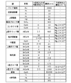
- FIG. 2 is a diagram showing a configuration of each layer included in the semiconductor light emitting device according to the embodiment.
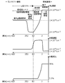
- FIG. 3 is a graph showing the distribution of Mg and carbon concentrations and Al composition ratio with respect to a part of the electron barrier layer (constant composition region) and the position of the p-type clad layer in the stacking direction according to the embodiment.
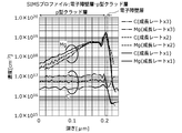
- FIG. 4 is a graph showing the distribution of the concentrations of Mg and carbon with respect to the positions of the electron barrier layer and the p-type clad layer in the stacking direction according to the embodiment.
- FIG. 1 is a schematic cross-sectional view showing the overall configuration of the semiconductor light emitting device according to the embodiment.
- FIG. 2 is a diagram showing a configuration of each layer included in the semiconductor light emitting device according to the embodiment.
- FIG. 3 is a graph showing the distribution of Mg and carbon concentrations and Al composition ratio with
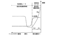
- FIG. 5 is a graph showing the distribution of the concentrations of Mg and carbon with respect to the position in the stacking direction of the p-type clad layer according to the embodiment.
- FIG. 6 is a graph showing a method for manufacturing the electron barrier layer and the p-type clad layer according to the embodiment.
- each figure is a schematic diagram and is not necessarily exactly illustrated. Therefore, the scales and the like do not always match in each figure.
- substantially the same configuration is designated by the same reference numerals, and duplicate description will be omitted or simplified.
- the terms “upper” and “lower” do not refer to the upward direction (vertically upward) and the downward direction (vertically downward) in absolute spatial recognition, but are based on the stacking order in the stacking configuration. It is used as a term defined by the relative positional relationship with. Also, the terms “upper” and “lower” are used not only when the two components are spaced apart from each other and another component exists between the two components, but also when the two components It also applies when they are placed in contact with each other.
- FIG. 1 is a schematic cross-sectional view showing the overall configuration of the semiconductor light emitting device 10 according to the present embodiment.
- FIG. 2 is a diagram showing a configuration of each layer included in the semiconductor light emitting device 10 according to the present embodiment.
- FIG. 2 shows the material, In composition ratio or Al composition ratio, film thickness, impurities (that is, dopant) and their concentrations of each layer of the semiconductor light emitting device 10.
- the semiconductor light emitting element 10 shown in FIGS. 1 and 2 is a semiconductor element that emits light when a current is supplied.
- the semiconductor light emitting device 10 is a semiconductor laser device that emits laser light.
- FIG. 1 shows a cross section of the semiconductor light emitting device 10 perpendicular to the laser resonance direction.
- the semiconductor light emitting device 10 includes a light emitting layer 15, an electron barrier layer 18, and a p-type clad layer 19.
- the semiconductor light emitting device 10 includes a substrate 11, an n-type clad layer 13, an n-side guide layer 14, a p-side guide layer 16, an intermediate layer 17, a contact layer 20, and a current block layer. 21, a p-side electrode 22, a pad electrode 23, an n-side electrode 24, and an adhesion auxiliary layer 25 are further provided.
- the substrate 11 is a substrate of the semiconductor light emitting element 10.
- the substrate 11 is, for example, a group III nitride semiconductor substrate.
- Each semiconductor layer of the semiconductor light emitting element 10 is arranged above the main surface of the substrate 11.
- the substrate 11 is a hexagonal n-type GaN substrate having a thickness of 85 ⁇ m.
- the substrate 11 is doped with Si having a concentration of 1 ⁇ 10 18 cm -3 as an impurity.
- the n-type clad layer 13 is an example of a first conductive type clad layer arranged above the substrate 11.
- the first conductive type is n-type
- the n-type clad layer 13 is an Al 0.035 Ga 0.965 N layer having a film thickness of 1500 nm.
- the n-type clad layer 13 is doped with Si having a concentration of 1 ⁇ 10 18 cm -3 as an impurity.
- the n-side guide layer 14 is a layer above the n-type clad layer 13 and below the light-emitting layer 15 and has a higher refractive index than the n-type clad layer 13, and has a function of confining light in the vicinity of the light-emitting layer 15.
- the n-side guide layer 14 is a GaN layer having a film thickness of 100 nm and doped with Si having a concentration of 1 ⁇ 10 18 cm -3 as an impurity, which are laminated in order from the n-type clad layer 13 side. , With a film thickness of 175 nm and an undoped In 0.03 Ga 0.97 N layer.
- the light emitting layer 15 is a layer that generates light in the semiconductor light emitting device 10, and is an active layer made of a group III nitride semiconductor. In this embodiment, the light emitting layer 15 is an undoped quantum well active layer.
- the light emitting layer 15 is an active layer having a quantum well structure in which quantum well layers made of InGaN and quantum barrier layers made of InGaN are alternately laminated. More specifically, the light emitting layer 15 includes a barrier layer composed of an In 0.04 Ga 0.96 N layer having a film thickness of 7 nm and an In having a film thickness of 2.8 nm, which are laminated in order from the n-side guide layer 14 side.
- the p-side guide layer 16 is a layer above the light emitting layer 15 and below the p-type clad layer 19 and having a higher refractive index than the p-type clad layer 19, and has a function of confining light in the vicinity of the light emitting layer 15.
- the p-side guide layer 16 has a film thickness of 98 nm and includes an undoped In 0.03 Ga 0.97 N layer.
- the intermediate layer 17 is a layer arranged between the p-side guide layer 16 and the electron barrier layer 18.
- the intermediate layer 17 is an undoped InGaN layer having a film thickness of 21 nm and having a film thickness of 3 nm and a concentration of 2 ⁇ 10 19 cm -3 as impurities, which are laminated in order from the p-side guide layer 16 side.
- the In composition ratio of the undoped InGaN layer contained in the intermediate layer 17 gradually decreases from 3% to 0% from the p-side guide layer 16 side end toward the electron barrier layer 18 side end.
- the electron barrier layer 18 is arranged above the light emitting layer 15 and is a layer made of a group III nitride semiconductor containing Al. This is a barrier layer for suppressing the leakage of electrons to the p-type clad layer 19.
- the electron barrier layer 18 is laminated in order from the intermediate layer 17 side, has a film thickness of 5 nm, is doped with Mg having a concentration of 2 ⁇ 10 19 cm -3 as an impurity, and has an Al composition x of 2%.
- Al x Ga 1-x N layer is changed with an inclination up to 36% and (graded composition region), Al in a thickness of 2 nm, Mg of concentration of 2 ⁇ 10 19 cm -3 is doped as an impurity 0 Includes .36 Ga 0.64 N layer (constant composition region).
- the Mg concentration in the electron barrier layer 18 may be, for example, 1 ⁇ 10 17 cm -3 or more and 1 ⁇ 10 20 cm -3 or less.
- the p-type clad layer 19 is an example of a second conductive type clad layer arranged above the electron barrier layer 18 in contact with the electron barrier layer 18.
- the p-type clad layer 19 is a layer having a lower refractive index and a higher bandgap energy than the light emitting layer 15. Since the refractive index of the p-type clad layer 19 is lower than the refractive index of the light emitting layer 15, light can be confined in the light emitting layer 15. Further, since the bandgap energy of the p-type clad layer 19 is higher than the bandgap energy of the light emitting layer 15, the absorption of light in the p-type clad layer 19 can be suppressed.
- the second conductive type is a conductive type different from the first conductive type.
- the second conductive type is p-type
- the p-type clad layer 19 has a film thickness of 660 nm and a concentration of 2 ⁇ 10 18 cm -3 or more and 1 ⁇ 10 19 cm -3 or less as impurities. It is an Al 0.035 Ga 0.965 N layer doped with Mg. The detailed configuration of the p-type clad layer 19 will be described later.
- the contact layer 20 is a layer that makes ohmic contact with the p-side electrode 22.
- the contact layer 20 is a GaN layer laminated in order from the p-type clad layer 19 side and doped with Mg having a film thickness of 50 nm and a concentration of 2 ⁇ 10 19 cm -3 as an impurity, and a film thickness of 10 nm. It contains a GaN layer doped with Mg having a concentration of 2 ⁇ 10 20 cm -3 as an impurity.
- the p-type clad layer 19 has a convex portion protruding from the n-side electrode 24 toward the p-side electrode 22. Further, the contact layer 20 is provided on the convex portion of the p-type clad layer 19. The ridge portion 19r is formed by the convex portion of the p-type clad layer 19 and the contact layer 20.
- the current block layer 21 is an insulating layer among the contact layer 20 and the p-type clad layer 19 that blocks the current flowing outside the ridge portion 19r.
- the current block layer 21 covers the p-type clad layer 19 exposed from the contact layer 20.
- the contact layer 20 on the upper surface of the ridge portion 19r is not covered by the current block layer 21, but is exposed from the current block layer 21.
- the current block layer 21 is a SiO 2 film having a film thickness of 300 nm.
- the p-side electrode 22 is an electrode that makes ohmic contact with the contact layer 20.
- the p-side electrode 22 is arranged on the upper surface of the contact layer 20, that is, the upper surface of the ridge portion 19r.
- the p-side electrode 22 includes a Pd film having a film thickness of 40 nm and a Pt film having a film thickness of 35 nm, which are laminated in order from the contact layer 20 side.
- the pad electrode 23 is a pad-shaped electrode arranged above the p-side electrode 22. In the present embodiment, the pad electrode 23 is arranged on the p-side electrode 22 and the current block layer 21.
- the pad electrode 23 is an Au film having a film thickness of 2 ⁇ m.
- the adhesion auxiliary layer 25 is provided to improve the adhesion of the pad electrode 23 to the current block layer 21.
- the close contact auxiliary layer 25 is provided in contact with each other between the pad electrode 23 and the current block layer 21.
- Adhesion auxiliary layers 25 are provided on both sides of the ridge, for example.
- the adhesion auxiliary layer 25 is formed by using a metal material.
- the adhesion auxiliary layer 25 has a laminated structure of a Ti film having a film thickness of 10 nm and a Pt film having a film thickness of 50 nm. The Ti film is located on the lower layer side and is in contact with the current block layer 21.
- the n-side electrode 24 is an electrode arranged on the lower surface of the substrate 11 (that is, the main surface on the back side of the main surface on which the n-type clad layer 13 of the substrate 11 is arranged).
- the n-side electrode 24 includes a Ti film having a film thickness of 10 nm, a Pt film having a film thickness of 35 nm, and an Au film having a film thickness of 300 nm, which are laminated in order from the substrate 11 side.
- FIG. 3 is a graph showing the concentrations of Mg and carbon with respect to a part of the electron barrier layer 18 (constant composition region) and the position of the p-type clad layer 19 in the stacking direction according to the present embodiment, and the distribution of the Al composition ratio. Is. In FIG. 3, the distributions of Mg concentration, carbon concentration, and Al composition ratio are shown in order from the top.
- the stacking direction means the thickness direction in which each semiconductor layer is laminated, that is, the direction perpendicular to the main surface of the substrate 11.
- the horizontal axis of each graph in FIG. 3 represents the thickness, and the position 5 nm from the end of the electron barrier layer 18 on the light emitting layer 15 side, that is, the boundary between the inclined composition region and the constant composition region is used as a reference (0 nm).
- the horizontal axis of each graph in FIG. 3 represents the distance in the film thickness direction from the boundary between the inclined composition region and the constant composition region.
- the thickness increases as it approaches the contact layer 20.
- the vertical axes of the upper, middle, and lower graphs indicate the Mg concentration, the carbon concentration, and the Al composition ratio, respectively.
- the constant composition region of the electron barrier layer 18 and the p-type clad layer 19 contain Mg as a dopant.
- the Mg concentration in the constant composition region of the electron barrier layer 18, the Mg concentration is about 2 ⁇ 10 19 cm -3 , and the carbon concentration is about 1 ⁇ 10 16 cm -3.
- the inclined composition region of the electron barrier layer 18 is not shown in the upper graph of FIG. 3, the Mg concentration is about 2 ⁇ 10 19 cm -3 and the carbon concentration is 1 ⁇ even in the inclined composition region. It is about 10 16 cm -3.
- the Al composition is different in the constant composition region and the inclined composition region of the electron barrier layer 18, the Mg concentration and the carbon concentration are the same.
- the electron barrier layer 18 includes a region in which the concentration ratio of carbon to Mg is 1 ⁇ 10 -3 or less. By forming a region having a high Mg concentration in the electron barrier layer 18 in this way, the resistance of the electron barrier layer 18 can be reduced.
- the p-type clad layer 19 has a high carbon concentration region containing carbon (a region from 2 nm to 82 nm in thickness) and a low carbon concentration region (thickness 82 nm or more) having a lower carbon concentration than the high carbon concentration region, in this order from the electron barrier layer 18 side. Area) and includes.
- the carbon concentration in the high carbon concentration region is about 1 ⁇ 10 17 cm -3
- the carbon concentration in the low carbon concentration region is about 2 ⁇ 10 16 cm -3
- the carbon concentration in the electron barrier layer 18 is about 1 ⁇ 10 16 cm -3.
- the carbon concentration in the p-type clad layer 19 can be realized, for example, by changing the growth rate (that is, the crystal growth rate) of the p-type clad layer 19.
- FIG. 4 is a graph showing the distribution of the concentrations of Mg and carbon with respect to the positions of the electron barrier layer 18 and the p-type clad layer 19 in the stacking direction according to the present embodiment.
- the horizontal axis of the graph of FIG. 4 represents the depth, and the depth at a position where the distance from the electron barrier layer 18 of the p-type clad layer 19 is about 0.2 ⁇ m is set to 0 nm, and as it advances toward the electron barrier layer 18, The depth increases.
- the carbon contained in the p-type clad layer 19 is considered to be derived from the raw material gas used to form the p-type clad layer 19. It is considered that the Mg concentration decreases because the amount of Mg taken up is suppressed by increasing the carbon concentration by increasing the growth rate in this way. Further, as the carbon concentration increases, the crystal quality of the p-type clad layer 19 deteriorates. Therefore, in the present embodiment, when forming a region of the p-type clad layer 19 where the influence of residual Mg is large, that is, a region relatively close to the electron barrier layer 18, the growth rate is increased and the electron barrier layer is formed.
- the p-type clad layer 19 has a high carbon concentration region containing carbon and a low carbon concentration region having a lower carbon concentration than the high carbon concentration region in this order from the electron barrier layer 18 side. Including.
- the Mg concentration in the region where the light intensity is higher can be suppressed.
- the light absorption loss due to Mg in the p-type clad layer can be suppressed. That is, it is possible to suppress an increase in light absorption loss in the p-type clad layer 19 due to the provision of the electron barrier layer 18 in the semiconductor light emitting device 10.
- the p-type clad layer 19 includes a low carbon concentration region having a lower carbon concentration than the high carbon concentration region, the crystal quality of the p-type clad layer 19 is higher than that in the case where the entire p-type clad layer 19 has a high carbon concentration region. Can be suppressed.
- the uptake of Mg into the p-type clad layer 19 can be suppressed, so that the high carbon concentration region is a decreasing region in which the Mg concentration decreases as the distance from the electron barrier layer 18 increases. including.
- the Mg concentration can be sharply reduced with respect to the depth.
- the region having a thickness of 2 nm to 82 nm shown in FIG. 3 corresponds to the reduced region.
- the reduced region is a region separated by 50 nm or more from the interface between the p-type clad layer 19 and the electron barrier layer 18, and the rate of change of Mg concentration with respect to the position in the stacking direction is 0.5 ⁇ 10 17 cm -3 / nm or more. Includes the area of. As described above, when the p-type clad layer 19 includes a region in which the Mg concentration sharply decreases, it is possible to suppress an increase in light absorption loss in the p-type clad layer 19 due to the provision of the electron barrier layer 18.
- the p-type clad layer 19 includes a low Mg concentration region containing Mg and a high Mg concentration region which is arranged above the low Mg concentration region and has a higher Mg concentration than the low Mg concentration region.
- the p-type clad layer 19 includes the low Mg concentration region closer to the electron barrier layer 18 than the high Mg concentration region, the light absorption loss in the p-type clad layer 19 due to the provision of the electron barrier layer 18 Can be suppressed.
- the p-type clad layer 19 includes a high Mg concentration region, the resistance of the clad layer can be reduced. In the upper graph of FIG. 3, only a part of the low carbon concentration region is shown as the low Mg concentration region, but the low Mg concentration region may be included in the high carbon concentration region.
- FIG. 5 is a graph showing the distribution of the concentrations of Mg and carbon with respect to the position in the stacking direction of the p-type clad layer 19 according to the present embodiment.
- the horizontal axis of the graph of FIG. 5 shows the thickness as in FIG. 3, and the vertical axis shows the concentrations of Mg and carbon.
- the vertical axis represents the concentration in which each of the Mg concentration and the carbon concentration is individually standardized.
- the carbon concentration is substantially uniform.
- the Mg concentration decreases in the high carbon concentration region as described above. That is, in the region close to the electron barrier layer 18, the effect of residual Mg after the formation of the electron barrier layer 18 increases the Mg concentration, and in the region away from the electron barrier layer 18, the effect of residual Mg is reduced. The concentration becomes low. Therefore, the p-type clad layer 19 has a low concentration ratio region R1 having a small concentration ratio of carbon to Mg arranged in a region close to the electron barrier layer 18 and an upper portion of the low concentration ratio region R1 (that is, the contact layer 20 side).
- the p-type clad layer 19 has a carbon concentration of about 1 ⁇ 10 17 cm -3 and a Mg concentration of 1 ⁇ 10 19 cm in the low concentration ratio region R1 as shown in FIG. It includes a region of -3 or more, that is, a region in which the concentration ratio of carbon to Mg is 1% or less.
- the p-type clad layer 19 includes the low concentration ratio region R1 having a low Mg concentration closer to the electron barrier layer than the high concentration ratio region R2, so that the p-type clad layer 18 is provided with the electron barrier layer 18. The increase in light absorption loss in 19 can be suppressed.
- Each semiconductor layer of the semiconductor light emitting device 10 can be sequentially formed on the main surface of the substrate 11 by using an organic metal vapor phase growth method (MOCVD) or the like.
- MOCVD organic metal vapor phase growth method
- the ridge portion 19r can be formed by using photolithography and etching.
- the current block layer 21 can be formed by using a plasma CVD (Chemical Vapor Deposition) method or the like.
- the portion formed on the contact layer 20 of the ridge portion 19r (that is, the portion in contact with the contact layer 20) is removed by using photolithography and etching. Subsequently, the p-side electrode 22 is formed only above the ridge portion 19r by using the vacuum deposition method and the lift-off method.
- a contact auxiliary layer 25 having a predetermined shape is formed on the current block layer 21.
- the adhesion auxiliary layer 25 is formed by using a metal film film formation and a lift-off method.
- the metal film includes a laminated film of a Ti film and a Pt film, and is formed by a vapor deposition method or a sputtering method.
- the adhesion auxiliary layer 25 is formed only on the current block layer 21, and does not come into contact with the p-type contact layer 20 and the p-side electrode 22.
- the pad electrode 23 is formed by using the vacuum deposition method and the lift-off method. Further, an n-side electrode 24 is formed on the lower surface of the substrate 11 by using a vacuum deposition method and a lift-off method.
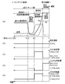
- FIG. 6 is a graph showing a method for manufacturing the electron barrier layer 18 and the p-type clad layer 19 according to the present embodiment.
- FIG. 6A is a graph showing the concentration of Mg and carbon with respect to the constant composition region of the electron barrier layer 18 and the position (thickness) of the p-type clad layer 19 in the stacking direction, and the distribution of the Al composition ratio. ..
- the horizontal axis of the graph (a) shows the thickness corresponding to the position in the stacking direction as in the horizontal axis of FIG.
- the Mg concentration, the carbon concentration, and the Al composition ratio are shown by curves of a solid line, a broken line, and a dotted line, respectively.
- the vertical axis is the concentration in which each of Mg concentration, carbon concentration and Al concentration is individually standardized. Represents.
- Graph (b) of FIG. 6 shows the relationship between the time spent for crystal growth (horizontal axis) of the constant composition region of the electron barrier layer 18 and each layer of the p-type clad layer 19 and the growth temperature (vertical axis). The time on the horizontal axis is associated with the thickness of the graph (a).
- the graphs (c), (d), and (e) of FIG. 6 show the constant composition region of the electron barrier layer 18, the time spent for crystal growth of each layer of the p-type clad layer 19 (horizontal axis), and the electron barrier layer 18 The relationship between the constant composition region and the supply amount (vertical axis) of each raw material gas forming the p-type clad layer 19 is shown.
- the graphs (c), (d), and (e) of FIG. 6 show the supply amounts of TMG (trimethylgallium), Cp2Mg (biscyclopentadienyl magnesium), and TMA (trimethylaluminum), respectively.
- the constant composition region of the electron barrier layer 18 and the growth temperature of the p-type clad layer 19 are constant at 970 ° C.
- the electron barrier layer 18 made of a group III nitride semiconductor containing Al is formed on the intermediate layer 17. Following the composition gradient region of the electron barrier layer 18, a constant composition region is formed. As shown in FIG. 6, the TMG supply amount, Cp2Mg supply amount, and TMA supply amount at the time of forming the constant composition region of the electron barrier layer 18 are 1.9 mL / min, 8 mL / min, and 8.3 mL, respectively. / Min. As described above, by supplying Cp2Mg at the time of forming the constant composition region of the electron barrier layer 18, Mg is supplied as a dopant.
- the amount of each raw material gas supplied when the constant composition region of the electron barrier layer 18 is formed is constant.
- the crystal growth in the constant composition region of the electron barrier layer 18 is continued until the film thickness reaches 2 nm (that is, only the crystal growth time corresponding to the film thickness of 2 nm).
- the crystal growth of the p-type clad layer 19 is started.
- a high carbon concentration region in contact with a constant composition region of the electron barrier layer 18 of the p-type clad layer 19 is formed.
- the TMG supply amount, Cp2Mg supply amount, and TMA supply amount at the time of forming the high carbon concentration region are 18 mL / min, 0 mL / min, and 10 mL / min, respectively. As described above, it is not necessary to supply the raw material gas containing Mg in the crystal growth in the high carbon concentration region.
- Mg is doped into the p-type clad layer 19 by the residual Mg even if the raw material gas containing Mg is not supplied.
- Crystal growth in the high carbon concentration region is continued until the film thickness reaches 80 nm.
- a low carbon concentration region is formed on the high carbon concentration region of the p-type clad layer 19.
- a low Mg concentration region is formed.
- the TMG supply amount, Cp2Mg supply amount, and TMA supply amount at the time of forming the low Mg concentration region are 6 mL / min, 1.2 mL / min, and 3.5 mL / min, respectively. Crystal growth in the low Mg concentration region continues until the film thickness reaches 170 nm.
- the TMG supply amount, Cp2Mg supply amount, and TMA supply amount at the time of forming the high Mg concentration region are 6 mL / min, 6 mL / min, and 3.5 mL / min, respectively. Crystal growth in the low Mg concentration region continues until the film thickness reaches 410 nm.
- the electron barrier layer 18 and the p-type clad layer 19 according to the present embodiment can be formed. Further, as described above, in the method for manufacturing the semiconductor light emitting device 10 according to the present embodiment, in the step of forming a constant composition region of the electron barrier layer 18, Mg is supplied as a dopant to form the p-type clad layer 19. In the process, the growth rate is changed. As described above, by changing the growth rate in the step of forming the p-type clad layer 19, the p-type clad layer 19 includes a region formed at a high growth rate.
- the p-type clad layer 19 includes a region in which the Mg concentration is suppressed. it can. As a result, it is possible to suppress an increase in light absorption loss in the p-type clad layer 19 due to the provision of the electron barrier layer 18.
- the growth rate is changed by changing the Ga supply amount. Specifically, in the high carbon concentration region, the TMG supply amount corresponding to the Ga supply amount is set to 18 mL / min, and in the low carbon concentration region, the TMG supply amount is set to 6 mL / min.
- the amount of Mg incorporated into the p-type clad layer 19 can be changed. Since the Mg concentration can be suppressed in the region where the Ga supply amount is large, the increase in light absorption loss in the p-type clad layer 19 due to the provision of the electron barrier layer 18 can be suppressed.
- the amount of Ga supplied in the step of forming the p-type clad layer 19 is larger immediately before the end of the step of forming the p-type clad layer 19 than immediately after the start of the step of forming the p-type clad layer 19. In other words, the amount of Ga supplied is larger in the low carbon concentration region than in the high carbon concentration region.
- the Mg concentration in the region adjacent to the electron barrier layer 18 in the p-type clad layer 19 can be suppressed. Therefore, since the Mg concentration can be suppressed in the region of the p-type clad layer 19 having the highest light intensity, the increase in light absorption loss in the p-type clad layer 19 due to the provision of the electron barrier layer 18 can be further suppressed.
- the Cp2Mg supply amount (that is, the Mg supply amount) is increased stepwise in the low carbon concentration region, but it may be continuously increased.
- the Mg supply amount in the low carbon concentration region, it is possible to increase the Mg concentration of the entire p-type clad layer 19 while suppressing the Mg concentration in the region near the light emitting layer 15. Therefore, the resistance of the p-type clad layer 19 can be reduced while suppressing an increase in the light absorption loss of the p-type clad layer 19.
- the p-type clad layer 19 includes a low Mg concentration region and a high Mg concentration region arranged on the low Mg concentration region, but is closer to the electron barrier layer 18 than the low Mg concentration region.
- a region having a high Mg concentration may be formed.
- a superlattice structure may be applied to the p-type clad layer 19 according to the above embodiment.
- Such a superlattice structure can be formed by intermittently supplying TMA, for example, when forming a p-type clad layer.
- the semiconductor light emitting element is a semiconductor laser element
- the semiconductor light emitting element is not limited to the semiconductor laser element.
- the semiconductor light emitting device may be a superluminescent diode.
- a buffer layer may be formed between the substrate 11 and the n-type clad layer 13.
- the buffer layer is a layer for suppressing distortion caused by lattice mismatch between the substrate 11 and the n-type clad layer 13.
- the buffer layer is an Al 0.01 Ga 0.99 N layer having a film thickness of 100 nm.
- the semiconductor light emitting device of the present disclosure can be applied to a projector, lighting, a laser machine, etc. as a high output and highly efficient light source, for example.
Landscapes
- Physics & Mathematics (AREA)
- Condensed Matter Physics & Semiconductors (AREA)
- General Physics & Mathematics (AREA)
- Electromagnetism (AREA)
- Optics & Photonics (AREA)
- Chemical & Material Sciences (AREA)
- Geometry (AREA)
- General Chemical & Material Sciences (AREA)
- Inorganic Chemistry (AREA)
- Chemical Kinetics & Catalysis (AREA)
- Engineering & Computer Science (AREA)
- Materials Engineering (AREA)
- Mechanical Engineering (AREA)
- Metallurgy (AREA)
- Organic Chemistry (AREA)
- Semiconductor Lasers (AREA)
Priority Applications (2)
| Application Number | Priority Date | Filing Date | Title |
|---|---|---|---|
| JP2021554956A JP7642553B2 (ja) | 2019-11-08 | 2020-11-04 | 半導体発光素子、及び半導体発光素子の製造方法 |
| US17/723,963 US12438342B2 (en) | 2019-11-08 | 2022-04-19 | Semiconductor light-emitting element and method of fabricating semiconductor light-emitting element |
Applications Claiming Priority (2)
| Application Number | Priority Date | Filing Date | Title |
|---|---|---|---|
| JP2019-203485 | 2019-11-08 | ||
| JP2019203485 | 2019-11-08 |
Related Child Applications (1)
| Application Number | Title | Priority Date | Filing Date |
|---|---|---|---|
| US17/723,963 Continuation US12438342B2 (en) | 2019-11-08 | 2022-04-19 | Semiconductor light-emitting element and method of fabricating semiconductor light-emitting element |
Publications (1)
| Publication Number | Publication Date |
|---|---|
| WO2021090849A1 true WO2021090849A1 (ja) | 2021-05-14 |
Family
ID=75848546
Family Applications (1)
| Application Number | Title | Priority Date | Filing Date |
|---|---|---|---|
| PCT/JP2020/041250 Ceased WO2021090849A1 (ja) | 2019-11-08 | 2020-11-04 | 半導体発光素子、及び半導体発光素子の製造方法 |
Country Status (3)
| Country | Link |
|---|---|
| US (1) | US12438342B2 (cg-RX-API-DMAC7.html) |
| JP (1) | JP7642553B2 (cg-RX-API-DMAC7.html) |
| WO (1) | WO2021090849A1 (cg-RX-API-DMAC7.html) |
Cited By (4)
| Publication number | Priority date | Publication date | Assignee | Title |
|---|---|---|---|---|
| WO2024204634A1 (ja) * | 2023-03-30 | 2024-10-03 | 旭化成株式会社 | 窒化物半導体素子、窒化物半導体積層体の製造方法及び窒化物半導体素子の製造方法 |
| WO2024204635A1 (ja) * | 2023-03-30 | 2024-10-03 | 旭化成株式会社 | 窒化物半導体積層体及び窒化物半導体素子の製造方法、並びに窒化物半導体素子 |
| JPWO2024204636A1 (cg-RX-API-DMAC7.html) * | 2023-03-30 | 2024-10-03 | ||
| WO2024257516A1 (ja) * | 2023-06-12 | 2024-12-19 | パナソニックホールディングス株式会社 | 窒化物半導体発光素子及び窒化物半導体発光素子の製造方法 |
Citations (4)
| Publication number | Priority date | Publication date | Assignee | Title |
|---|---|---|---|---|
| JP2010056158A (ja) * | 2008-08-26 | 2010-03-11 | Sumitomo Electric Ind Ltd | 窒化物系半導体光素子を製造する方法、及びエピタキシャルウエハを製造する方法 |
| JP2011023541A (ja) * | 2009-07-15 | 2011-02-03 | Sumitomo Electric Ind Ltd | Iii族窒化物半導体光素子及びエピタキシャル基板 |
| JP2012186413A (ja) * | 2011-03-08 | 2012-09-27 | Toshiba Corp | 半導体発光素子およびその製造方法 |
| US20150243841A1 (en) * | 2014-02-22 | 2015-08-27 | Sensor Electronic Technology, Inc. | Semiconductor Structure with Stress-Reducing Buffer Structure |
Family Cites Families (4)
| Publication number | Priority date | Publication date | Assignee | Title |
|---|---|---|---|---|
| WO2007013257A1 (ja) | 2005-07-29 | 2007-02-01 | Matsushita Electric Industrial Co., Ltd. | 窒化物系半導体素子 |
| JP2009152448A (ja) | 2007-12-21 | 2009-07-09 | Dowa Electronics Materials Co Ltd | 窒化物半導体素子およびその製造方法 |
| JP7182344B2 (ja) * | 2018-03-13 | 2022-12-02 | 株式会社フジクラ | 半導体光素子、半導体光素子形成用構造体及びこれを用いた半導体光素子の製造方法 |
| JP7141425B2 (ja) * | 2020-04-28 | 2022-09-22 | 日機装株式会社 | 窒化物半導体発光素子 |
-
2020
- 2020-11-04 JP JP2021554956A patent/JP7642553B2/ja active Active
- 2020-11-04 WO PCT/JP2020/041250 patent/WO2021090849A1/ja not_active Ceased
-
2022
- 2022-04-19 US US17/723,963 patent/US12438342B2/en active Active
Patent Citations (4)
| Publication number | Priority date | Publication date | Assignee | Title |
|---|---|---|---|---|
| JP2010056158A (ja) * | 2008-08-26 | 2010-03-11 | Sumitomo Electric Ind Ltd | 窒化物系半導体光素子を製造する方法、及びエピタキシャルウエハを製造する方法 |
| JP2011023541A (ja) * | 2009-07-15 | 2011-02-03 | Sumitomo Electric Ind Ltd | Iii族窒化物半導体光素子及びエピタキシャル基板 |
| JP2012186413A (ja) * | 2011-03-08 | 2012-09-27 | Toshiba Corp | 半導体発光素子およびその製造方法 |
| US20150243841A1 (en) * | 2014-02-22 | 2015-08-27 | Sensor Electronic Technology, Inc. | Semiconductor Structure with Stress-Reducing Buffer Structure |
Cited By (10)
| Publication number | Priority date | Publication date | Assignee | Title |
|---|---|---|---|---|
| WO2024204634A1 (ja) * | 2023-03-30 | 2024-10-03 | 旭化成株式会社 | 窒化物半導体素子、窒化物半導体積層体の製造方法及び窒化物半導体素子の製造方法 |
| WO2024204635A1 (ja) * | 2023-03-30 | 2024-10-03 | 旭化成株式会社 | 窒化物半導体積層体及び窒化物半導体素子の製造方法、並びに窒化物半導体素子 |
| JPWO2024204636A1 (cg-RX-API-DMAC7.html) * | 2023-03-30 | 2024-10-03 | ||
| JPWO2024204635A1 (cg-RX-API-DMAC7.html) * | 2023-03-30 | 2024-10-03 | ||
| JPWO2024204634A1 (cg-RX-API-DMAC7.html) * | 2023-03-30 | 2024-10-03 | ||
| WO2024204636A1 (ja) * | 2023-03-30 | 2024-10-03 | 旭化成株式会社 | 窒化物半導体素子、窒化物半導体積層体の製造方法、及び窒化物半導体素子の製造方法 |
| JP7880079B2 (ja) | 2023-03-30 | 2026-06-25 | 旭化成株式会社 | 窒化物半導体素子、窒化物半導体積層体の製造方法及び窒化物半導体素子の製造方法 |
| JP7880080B2 (ja) | 2023-03-30 | 2026-06-25 | 旭化成株式会社 | 窒化物半導体素子、窒化物半導体積層体の製造方法、及び窒化物半導体素子の製造方法 |
| JP7904573B2 (ja) | 2023-03-30 | 2026-08-13 | 旭化成株式会社 | 窒化物半導体積層体及び窒化物半導体素子の製造方法、並びに窒化物半導体素子 |
| WO2024257516A1 (ja) * | 2023-06-12 | 2024-12-19 | パナソニックホールディングス株式会社 | 窒化物半導体発光素子及び窒化物半導体発光素子の製造方法 |
Also Published As
| Publication number | Publication date |
|---|---|
| US12438342B2 (en) | 2025-10-07 |
| JPWO2021090849A1 (cg-RX-API-DMAC7.html) | 2021-05-14 |
| US20220247156A1 (en) | 2022-08-04 |
| JP7642553B2 (ja) | 2025-03-10 |
Similar Documents
| Publication | Publication Date | Title |
|---|---|---|
| US8044430B2 (en) | Nitride semiconductor light-emitting device comprising multiple semiconductor layers having substantially uniform N-type dopant concentration | |
| KR100998540B1 (ko) | Iii족 질화물계 반도체 발광 소자 | |
| US7652281B2 (en) | Light emitting diode | |
| US12438342B2 (en) | Semiconductor light-emitting element and method of fabricating semiconductor light-emitting element | |
| JP6223075B2 (ja) | 発光素子の製造方法及び発光素子 | |
| KR20140123410A (ko) | 자외선 발광 소자 | |
| KR100752007B1 (ko) | 3족 질화물계 화합물 반도체 발광 소자 및 그 제조 방법 | |
| US11984535B2 (en) | III-nitride semiconductor light-emitting device comprising barrier layers and well layers and method of producing the same | |
| US10580936B2 (en) | Group III nitride semiconductor light-emitting device and production method therefor | |
| KR20100098565A (ko) | 반도체 발광 소자 | |
| JP2005268581A (ja) | 窒化ガリウム系化合物半導体発光素子 | |
| AU2020200271A1 (en) | Semiconductor laser element and method for manufacturing the same | |
| CN103299495A (zh) | 氮化镓基半导体激光器元件和制造氮化镓基半导体激光器元件的方法 | |
| CN109428264A (zh) | 具有低阀值电流的半导体激光二极管 | |
| JP2019117950A (ja) | 電子部品 | |
| JP7607286B2 (ja) | 窒化物半導体発光素子 | |
| WO2023026816A1 (ja) | 窒化物半導体発光素子 | |
| JP2006210692A (ja) | 3族窒化物系化合物半導体発光素子 | |
| KR100853935B1 (ko) | 반도체 발광 다이오드 및 그의 제조방법 | |
| WO2021172171A1 (ja) | レーザ素子 | |
| KR100742989B1 (ko) | 질화갈륨계 발광 소자의 제조 방법 | |
| KR101510057B1 (ko) | 반도체 발광소자 | |
| US20250364787A1 (en) | Vertical cavity light-emitting element and manufacturing method thereof | |
| WO2025154816A1 (ja) | 紫外半導体発光素子及びその製造方法 | |
| WO2024111583A1 (ja) | 垂直共振器型発光素子及びその製造方法 |
Legal Events
| Date | Code | Title | Description |
|---|---|---|---|
| 121 | Ep: the epo has been informed by wipo that ep was designated in this application |
Ref document number: 20885530 Country of ref document: EP Kind code of ref document: A1 |
|
| ENP | Entry into the national phase |
Ref document number: 2021554956 Country of ref document: JP Kind code of ref document: A |
|
| NENP | Non-entry into the national phase |
Ref country code: DE |
|
| 122 | Ep: pct application non-entry in european phase |
Ref document number: 20885530 Country of ref document: EP Kind code of ref document: A1 |