WO2021085382A1 - Reflective mask blank and reflective mask - Google Patents
Reflective mask blank and reflective mask Download PDFInfo
- Publication number
- WO2021085382A1 WO2021085382A1 PCT/JP2020/040115 JP2020040115W WO2021085382A1 WO 2021085382 A1 WO2021085382 A1 WO 2021085382A1 JP 2020040115 W JP2020040115 W JP 2020040115W WO 2021085382 A1 WO2021085382 A1 WO 2021085382A1
- Authority
- WO
- WIPO (PCT)
- Prior art keywords
- layer
- absorption layer
- reflective mask
- mask blank
- reflective
- Prior art date
Links
- 238000010521 absorption reaction Methods 0.000 claims abstract description 171
- 239000000758 substrate Substances 0.000 claims abstract description 33
- 239000010410 layer Substances 0.000 claims description 292
- 239000000463 material Substances 0.000 claims description 25
- 239000011241 protective layer Substances 0.000 claims description 19
- 238000001228 spectrum Methods 0.000 claims description 16
- 229910052757 nitrogen Inorganic materials 0.000 claims description 9
- 229910052796 boron Inorganic materials 0.000 claims description 7
- 229910052804 chromium Inorganic materials 0.000 claims description 7
- 229910052715 tantalum Inorganic materials 0.000 claims description 7
- 229910045601 alloy Inorganic materials 0.000 claims description 6
- 239000000956 alloy Substances 0.000 claims description 6
- 229910052750 molybdenum Inorganic materials 0.000 claims description 6
- 229910052758 niobium Inorganic materials 0.000 claims description 5
- 229910052697 platinum Inorganic materials 0.000 claims description 5
- 229910052702 rhenium Inorganic materials 0.000 claims description 5
- 229910052703 rhodium Inorganic materials 0.000 claims description 5
- 229910052719 titanium Inorganic materials 0.000 claims description 5
- 229910052763 palladium Inorganic materials 0.000 claims description 4
- 229910052710 silicon Inorganic materials 0.000 claims description 4
- 229910052726 zirconium Inorganic materials 0.000 claims description 4
- 239000010408 film Substances 0.000 description 147
- 230000010363 phase shift Effects 0.000 description 37
- 230000000694 effects Effects 0.000 description 24
- 230000003287 optical effect Effects 0.000 description 20
- 229910004168 TaNb Inorganic materials 0.000 description 19
- 238000000034 method Methods 0.000 description 19
- 238000004088 simulation Methods 0.000 description 17
- 238000010586 diagram Methods 0.000 description 16
- 238000004140 cleaning Methods 0.000 description 14
- 239000006096 absorbing agent Substances 0.000 description 11
- 238000001900 extreme ultraviolet lithography Methods 0.000 description 11
- 238000005530 etching Methods 0.000 description 9
- 229910052760 oxygen Inorganic materials 0.000 description 9
- 238000004519 manufacturing process Methods 0.000 description 8
- 229910010413 TiO 2 Inorganic materials 0.000 description 7
- 230000002745 absorbent Effects 0.000 description 7
- 239000002250 absorbent Substances 0.000 description 7
- 239000011521 glass Substances 0.000 description 7
- 239000007788 liquid Substances 0.000 description 7
- 229910004298 SiO 2 Inorganic materials 0.000 description 6
- 239000007789 gas Substances 0.000 description 6
- 238000001659 ion-beam spectroscopy Methods 0.000 description 6
- 239000002184 metal Substances 0.000 description 6
- 238000009826 distribution Methods 0.000 description 5
- 229910052751 metal Inorganic materials 0.000 description 5
- IJGRMHOSHXDMSA-UHFFFAOYSA-N Atomic nitrogen Chemical compound N#N IJGRMHOSHXDMSA-UHFFFAOYSA-N 0.000 description 4
- 229910000929 Ru alloy Inorganic materials 0.000 description 4
- 229910003071 TaON Inorganic materials 0.000 description 4
- 230000007423 decrease Effects 0.000 description 4
- 238000007689 inspection Methods 0.000 description 4
- 239000000126 substance Substances 0.000 description 4
- 229910052799 carbon Inorganic materials 0.000 description 3
- 238000001312 dry etching Methods 0.000 description 3
- 238000010030 laminating Methods 0.000 description 3
- 238000001755 magnetron sputter deposition Methods 0.000 description 3
- 238000004544 sputter deposition Methods 0.000 description 3
- 230000003746 surface roughness Effects 0.000 description 3
- 239000010409 thin film Substances 0.000 description 3
- QGZKDVFQNNGYKY-UHFFFAOYSA-N Ammonia Chemical compound N QGZKDVFQNNGYKY-UHFFFAOYSA-N 0.000 description 2
- QAOWNCQODCNURD-UHFFFAOYSA-N Sulfuric acid Chemical compound OS(O)(=O)=O QAOWNCQODCNURD-UHFFFAOYSA-N 0.000 description 2
- 238000000560 X-ray reflectometry Methods 0.000 description 2
- QVGXLLKOCUKJST-UHFFFAOYSA-N atomic oxygen Chemical compound [O] QVGXLLKOCUKJST-UHFFFAOYSA-N 0.000 description 2
- 150000001875 compounds Chemical class 0.000 description 2
- 150000002500 ions Chemical class 0.000 description 2
- 150000004767 nitrides Chemical class 0.000 description 2
- 239000001301 oxygen Substances 0.000 description 2
- 238000012545 processing Methods 0.000 description 2
- 239000002356 single layer Substances 0.000 description 2
- 238000012546 transfer Methods 0.000 description 2
- 238000002834 transmittance Methods 0.000 description 2
- XLYOFNOQVPJJNP-UHFFFAOYSA-N water Substances O XLYOFNOQVPJJNP-UHFFFAOYSA-N 0.000 description 2
- 229910018072 Al 2 O 3 Inorganic materials 0.000 description 1
- 229910019912 CrN Inorganic materials 0.000 description 1
- CBENFWSGALASAD-UHFFFAOYSA-N Ozone Chemical compound [O-][O+]=O CBENFWSGALASAD-UHFFFAOYSA-N 0.000 description 1
- -1 Si 3 N 4 Inorganic materials 0.000 description 1
- 229910004541 SiN Inorganic materials 0.000 description 1
- VYPSYNLAJGMNEJ-UHFFFAOYSA-N Silicium dioxide Chemical compound O=[Si]=O VYPSYNLAJGMNEJ-UHFFFAOYSA-N 0.000 description 1
- 229910004535 TaBN Inorganic materials 0.000 description 1
- 229910052782 aluminium Inorganic materials 0.000 description 1
- 229910021529 ammonia Inorganic materials 0.000 description 1
- SWXQKHHHCFXQJF-UHFFFAOYSA-N azane;hydrogen peroxide Chemical compound [NH4+].[O-]O SWXQKHHHCFXQJF-UHFFFAOYSA-N 0.000 description 1
- 230000015572 biosynthetic process Effects 0.000 description 1
- 238000004364 calculation method Methods 0.000 description 1
- 239000011248 coating agent Substances 0.000 description 1
- 238000000576 coating method Methods 0.000 description 1
- 230000000052 comparative effect Effects 0.000 description 1
- 239000013078 crystal Substances 0.000 description 1
- 230000007547 defect Effects 0.000 description 1
- 230000001419 dependent effect Effects 0.000 description 1
- 238000011161 development Methods 0.000 description 1
- 230000018109 developmental process Effects 0.000 description 1
- 238000005516 engineering process Methods 0.000 description 1
- 238000007687 exposure technique Methods 0.000 description 1
- 238000011086 high cleaning Methods 0.000 description 1
- 229910052739 hydrogen Inorganic materials 0.000 description 1
- XEMZLVDIUVCKGL-UHFFFAOYSA-N hydrogen peroxide;sulfuric acid Chemical compound OO.OS(O)(=O)=O XEMZLVDIUVCKGL-UHFFFAOYSA-N 0.000 description 1
- 229910052746 lanthanum Inorganic materials 0.000 description 1
- 238000001459 lithography Methods 0.000 description 1
- 229910001092 metal group alloy Inorganic materials 0.000 description 1
- 150000002739 metals Chemical class 0.000 description 1
- 239000000203 mixture Substances 0.000 description 1
- 238000012986 modification Methods 0.000 description 1
- 230000004048 modification Effects 0.000 description 1
- 230000003647 oxidation Effects 0.000 description 1
- 238000007254 oxidation reaction Methods 0.000 description 1
- 239000002245 particle Substances 0.000 description 1
- 238000003672 processing method Methods 0.000 description 1
- 230000007261 regionalization Effects 0.000 description 1
- 238000011160 research Methods 0.000 description 1
- 229910052707 ruthenium Inorganic materials 0.000 description 1
- 239000004065 semiconductor Substances 0.000 description 1
- 230000035945 sensitivity Effects 0.000 description 1
- LIVNPJMFVYWSIS-UHFFFAOYSA-N silicon monoxide Inorganic materials [Si-]#[O+] LIVNPJMFVYWSIS-UHFFFAOYSA-N 0.000 description 1
- 229910052814 silicon oxide Inorganic materials 0.000 description 1
- 238000005477 sputtering target Methods 0.000 description 1
- 229910052727 yttrium Inorganic materials 0.000 description 1
Images


Classifications
-
- G—PHYSICS
- G03—PHOTOGRAPHY; CINEMATOGRAPHY; ANALOGOUS TECHNIQUES USING WAVES OTHER THAN OPTICAL WAVES; ELECTROGRAPHY; HOLOGRAPHY
- G03F—PHOTOMECHANICAL PRODUCTION OF TEXTURED OR PATTERNED SURFACES, e.g. FOR PRINTING, FOR PROCESSING OF SEMICONDUCTOR DEVICES; MATERIALS THEREFOR; ORIGINALS THEREFOR; APPARATUS SPECIALLY ADAPTED THEREFOR
- G03F1/00—Originals for photomechanical production of textured or patterned surfaces, e.g., masks, photo-masks, reticles; Mask blanks or pellicles therefor; Containers specially adapted therefor; Preparation thereof
- G03F1/22—Masks or mask blanks for imaging by radiation of 100nm or shorter wavelength, e.g. X-ray masks, extreme ultraviolet [EUV] masks; Preparation thereof
- G03F1/24—Reflection masks; Preparation thereof
-
- G—PHYSICS
- G03—PHOTOGRAPHY; CINEMATOGRAPHY; ANALOGOUS TECHNIQUES USING WAVES OTHER THAN OPTICAL WAVES; ELECTROGRAPHY; HOLOGRAPHY
- G03F—PHOTOMECHANICAL PRODUCTION OF TEXTURED OR PATTERNED SURFACES, e.g. FOR PRINTING, FOR PROCESSING OF SEMICONDUCTOR DEVICES; MATERIALS THEREFOR; ORIGINALS THEREFOR; APPARATUS SPECIALLY ADAPTED THEREFOR
- G03F1/00—Originals for photomechanical production of textured or patterned surfaces, e.g., masks, photo-masks, reticles; Mask blanks or pellicles therefor; Containers specially adapted therefor; Preparation thereof
- G03F1/26—Phase shift masks [PSM]; PSM blanks; Preparation thereof
- G03F1/32—Attenuating PSM [att-PSM], e.g. halftone PSM or PSM having semi-transparent phase shift portion; Preparation thereof
-
- G—PHYSICS
- G03—PHOTOGRAPHY; CINEMATOGRAPHY; ANALOGOUS TECHNIQUES USING WAVES OTHER THAN OPTICAL WAVES; ELECTROGRAPHY; HOLOGRAPHY
- G03F—PHOTOMECHANICAL PRODUCTION OF TEXTURED OR PATTERNED SURFACES, e.g. FOR PRINTING, FOR PROCESSING OF SEMICONDUCTOR DEVICES; MATERIALS THEREFOR; ORIGINALS THEREFOR; APPARATUS SPECIALLY ADAPTED THEREFOR
- G03F1/00—Originals for photomechanical production of textured or patterned surfaces, e.g., masks, photo-masks, reticles; Mask blanks or pellicles therefor; Containers specially adapted therefor; Preparation thereof
- G03F1/38—Masks having auxiliary features, e.g. special coatings or marks for alignment or testing; Preparation thereof
- G03F1/48—Protective coatings
-
- G—PHYSICS
- G03—PHOTOGRAPHY; CINEMATOGRAPHY; ANALOGOUS TECHNIQUES USING WAVES OTHER THAN OPTICAL WAVES; ELECTROGRAPHY; HOLOGRAPHY
- G03F—PHOTOMECHANICAL PRODUCTION OF TEXTURED OR PATTERNED SURFACES, e.g. FOR PRINTING, FOR PROCESSING OF SEMICONDUCTOR DEVICES; MATERIALS THEREFOR; ORIGINALS THEREFOR; APPARATUS SPECIALLY ADAPTED THEREFOR
- G03F1/00—Originals for photomechanical production of textured or patterned surfaces, e.g., masks, photo-masks, reticles; Mask blanks or pellicles therefor; Containers specially adapted therefor; Preparation thereof
- G03F1/54—Absorbers, e.g. of opaque materials
-
- G—PHYSICS
- G03—PHOTOGRAPHY; CINEMATOGRAPHY; ANALOGOUS TECHNIQUES USING WAVES OTHER THAN OPTICAL WAVES; ELECTROGRAPHY; HOLOGRAPHY
- G03F—PHOTOMECHANICAL PRODUCTION OF TEXTURED OR PATTERNED SURFACES, e.g. FOR PRINTING, FOR PROCESSING OF SEMICONDUCTOR DEVICES; MATERIALS THEREFOR; ORIGINALS THEREFOR; APPARATUS SPECIALLY ADAPTED THEREFOR
- G03F7/00—Photomechanical, e.g. photolithographic, production of textured or patterned surfaces, e.g. printing surfaces; Materials therefor, e.g. comprising photoresists; Apparatus specially adapted therefor
- G03F7/20—Exposure; Apparatus therefor
-
- G—PHYSICS
- G03—PHOTOGRAPHY; CINEMATOGRAPHY; ANALOGOUS TECHNIQUES USING WAVES OTHER THAN OPTICAL WAVES; ELECTROGRAPHY; HOLOGRAPHY
- G03F—PHOTOMECHANICAL PRODUCTION OF TEXTURED OR PATTERNED SURFACES, e.g. FOR PRINTING, FOR PROCESSING OF SEMICONDUCTOR DEVICES; MATERIALS THEREFOR; ORIGINALS THEREFOR; APPARATUS SPECIALLY ADAPTED THEREFOR
- G03F1/00—Originals for photomechanical production of textured or patterned surfaces, e.g., masks, photo-masks, reticles; Mask blanks or pellicles therefor; Containers specially adapted therefor; Preparation thereof
- G03F1/52—Reflectors
Definitions
- the present invention relates to a reflective mask utilizing the phase shift effect and a reflective mask blank from which the reflective mask can be obtained.
- Etreme Ultra Violet as an exposure method alternative to the conventional exposure technique using visible light or ultraviolet light (wavelength 365 to 193 nm), “ It is called “EUV”.) Lithography is being considered.
- EUV light having a shorter wavelength than ArF excimer laser light is used as the light source used for exposure.
- the EUV light refers to light having a wavelength in the soft X-ray region or the vacuum ultraviolet region, and specifically, light having a wavelength of about 0.2 to 100 nm.
- EUV light used for EUV lithography for example, EUV light having a wavelength ⁇ of about 13.5 nm is used.
- EUV light is easily absorbed by many substances, so the refractive optics system used in conventional exposure technology cannot be used. Therefore, in EUV lithography, a reflective optical system such as a reflective mask or a mirror is used. In EUV lithography, a reflective mask is used as a transfer mask.
- a reflective layer that reflects EUV light is formed on the substrate, and an absorption layer that absorbs EUV light is formed in a pattern on the reflective layer.
- the reflective mask uses a reflective mask blank formed by laminating a reflective layer and an absorbent layer on a substrate in this order from the substrate side as a base plate, and removes a part of the absorbent layer to form a predetermined pattern. You can get it.
- EUV light incident on the reflective mask is absorbed by the absorbing layer and reflected by the reflective layer.
- the reflected EUV light is imaged on the surface of the exposure material (wafer coated with resist) by the optical system.
- the opening of the absorption layer is transferred to the surface of the exposure material.
- EUV lithography EUV light is usually incident on the reflective mask from a direction inclined by about 6 ° and is reflected obliquely as well.
- TaN, TaBN shown in Patent Document 1, and the like have been used as the material of the absorption layer. These materials are usually used under the conditions of a reflectance of 2% or less and a film thickness of 60 nm or more under EUV light. Optically, it corresponds to the condition of a binary mask, and its effect as a phase shift mask is small.
- the transmittance of the absorption layer By adjusting the transmittance of the absorption layer, it is possible to obtain a reflective mask that utilizes the phase shift effect.
- the absorbing layer transmits light slightly, and the reflected light of the absorbing layer has a phase difference with the light reflected by the opening.
- a reflective mask By using a reflective mask utilizing such a phase shift effect, the contrast of the optical image on the wafer is improved and the exposure margin is increased.
- Patent Document 2 uses TaNb as the material of the absorbing layer.
- the optimum value of the reflectance of the absorbing layer is set to 4 to 15% as a relative value with the reflectance of the opening. This value is close to the optimum value of the transmittance of the conventional ArF phase shift mask. Since the reflectance of the opening is usually about 65%, the optimum value of the reflectance of the absorption layer is 2.5 to 10% in absolute value.
- the optimum value of the phase difference of the reflective mask using the phase shift is set to 175 to 185 degrees. This range includes 180 degrees, which is the optimum value of the phase difference of the conventional ArF phase shift mask.
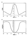
- FIG. 3A shows an example of the reflected light intensity distribution in the reflective mask using the phase shift effect
- FIG. 3B shows an example of the reflected light phase distribution in the reflective mask. It is a figure.
- the horizontal axes of FIGS. 3 (a) and 3 (b) indicate the positions in the width direction of the pattern when the position of the center of the pattern having a width of 64 nm is 0 nm.
- the reflected light intensity is maximized at the center of the pattern and continuously decreases toward the end (pattern edge) in the width direction of the pattern.
- the phase of the reflected light becomes a minimum at the center of the pattern, and the phase of the reflected light continuously changes toward the pattern edge. Due to this effect, the effective phase difference shifts. Therefore, in the case of the reflective mask, the optimum value of the phase difference of the absorbing layer is different from 180 degrees.
- the optical image intensity at the time of exposure is high because the exposure time is shortened and the throughput is advantageous. Therefore, it is preferable that the peak light intensity at the time of exposure is high.
- An object of the present invention is to provide a reflective mask for EUV lithography having a large phase shift effect and a high peak light intensity at the time of exposure, and a reflective mask blank for EUV lithography from which the reflective mask can be obtained.
- the present inventor has found a condition for the thickness of an absorption layer having a large phase shift effect and a high peak light intensity at the time of exposure in a reflective mask for EUV lithography. It was.
- NILS Normalized Image Log Slope, standardized image log slope
- NILS corresponds to the contrast of the optical image on the wafer.
- NILS is maximized when the absorption layer film thickness is 72 nm, and the phase shift effect is also maximized at this time.
- FIG. 4B shows the result of simulating the absorption layer film thickness dependence of the phase difference under the same conditions as above.
- the phase difference is about 210 degrees when the film thickness is 72 nm. This is because, as described above, the optimum value of the phase difference deviates from 180 degrees due to the influence of the continuous change of the phase of the reflected light toward the pattern edge. Since NILS is maximized at a film thickness of 72 nm, the effective phase difference is considered to be close to 180 degrees.
- FIG. 4C shows the result of simulating the film thickness dependence of the reflectance of the absorbing layer under the same conditions as above.
- the reflectance is maximized when the film thickness is 72 nm.
- the condition for maximizing the phase shift effect is when the effective phase difference is about 180 degrees and at the same time the reflectance is maximized. Therefore, the maximum value of NILS and the maximum value of reflectance match.
- NILS phase difference
- reflectance vibrate as the film thickness of the absorbing layer increases.
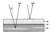
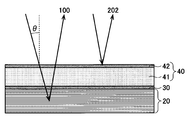
- the reason why such a phenomenon occurs is that, as shown in FIG. 5, interference occurs between the reflected light 100 from the reflecting layer 20 and the reflected light 200 on the surface of the absorbing layer 40.
- the maximum value of the reflectance corresponds to a position where interference is strengthened, that is, when the phases of the reflected light 100 and the reflected light 200 are aligned.
- the condition that the phases of the reflected light 100 and the reflected light 200 are aligned is obtained as follows. First, considering only the optical path length difference in the absorption layer 40, the condition that the phases of the reflected light 100 and the reflected light 200 are aligned is expressed by the following equation (1), where d is the film thickness of the absorption layer 40. .. In the above equation (1), N is an integer, ⁇ is the wavelength, n is the refractive index of the absorption layer 40, and ⁇ is the angle of incidence. In the case of the reflective mask for EUV lithography, the wavelength ⁇ is 13.53 nm and the incident angle ⁇ is 6 °.
- the phase shift on each reflecting surface is considered.
- the reflected light 100 is reflected inside the reflective layer 20.
- the phase shift at this time is ⁇ 0.64 radians according to the numerical calculation.
- the phase shift is tan -1 ( ⁇ k / (1-n)).
- n is the refractive index of the absorption layer 40 at a wavelength of 13.53 nm
- k is the absorption coefficient of the absorption layer 40 at the same wavelength.
- the condition for aligning the phases of the reflected light 100 and the reflected light 200 is given by the following equation (2) in consideration of the phase shift on the reflecting surface.
- the above equation (2) is a condition in which the reflected light 100 and the reflected light 200 are in phase with each other, that is, a condition in which the reflectance has a maximum value.
- the more effective phase difference needs to be about 180 degrees.
- the phase difference of the absorption layer 40 is about 210 degrees as shown in FIG. 4 (b).
- the difference in optical path length from that in vacuum when light reciprocates in the absorption layer 40 is 2 (1-n) d.
- Equation (3) the film thickness of the absorption layer having the maximum value of NILS is approximately the following equation (3).
- Equation (4) is a condition that the film thickness of the absorption layer should be satisfied in order to maximize the phase shift effect.
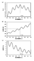
- FIG. 7 (a) shows the result of calculating the film thickness dependence of NILS by simulation
- FIG. 7 (b) shows the result of obtaining the film thickness dependence of peak light intensity by simulation
- FIG. 7 (c) shows the result. The result of simulating the film thickness dependence of the phase difference is shown.
- the thickness d MAX of the absorber layer NILS which is obtained by the above becomes the maximum value.
- the exposure conditions are the same as in FIG. Thickness d MAX of the absorber layer becomes 72.3nm than (4).
- the peak light intensity at the time of exposure increases as the film thickness becomes thinner.
- NILS reaches its maximum when the film thickness of the absorption layer is d MAX , and has a peak at d MAX -6 nm.
- the light intensity at the film thickness d MAX -6 nm is 6% higher than the light intensity at the film thickness d MAX.
- the optimum value of the film thickness of the absorption layer is either d MAX or d MAX -6 nm.
- the phase difference at the film thickness d MAX is 210 degrees
- the phase difference at the film thickness d MAX -6 nm is 203 degrees, both of which are far from 180 degrees.
- the optimum value of the phase difference is 190 to 220 degrees.
- NILS at a film thickness with a phase difference of 180 degrees is off the peak, and it can be seen that the phase difference of 180 degrees is not the optimum value for the film thickness of the absorption layer.
- the film thickness varies by about + -1 nm.
- the variation in the peak wavelength of the reflected light spectrum is about + ⁇ 0.1 nm. Therefore, if the film thickness d (nm) of the absorption layer satisfies d MAX -1 nm ⁇ d ⁇ d MAX + 1 nm, or (d MAX -6 nm) -1 nm ⁇ d ⁇ (d MAX -6 nm) + 1 nm, the phase shift The effect is large and the peak light intensity during exposure is high.
- equations can be summarized as the following equation (5).
- the integer i is 0 or 1.
- the absorption layer 40 is composed of two layers, a lower absorption layer 41 and an upper absorption layer 42.
- interference occurs between the reflected light 100 from the reflecting layer 20 and the reflected light 202 on the surface of the upper absorbing layer 42. Since the reflected light 202 is reflected on the surface of the upper absorption layer 42, the phase shift is tan -1 ( ⁇ k 2 / (1-n 2 )).
- k 2 is the absorption coefficient of the upper absorption layer 42 at a wavelength of 13.53 nm
- n 2 is the refractive index of the upper absorption layer at the same wavelength.
- the condition that the phases of the reflected light 100 and the reflected light 200 are aligned is given by the following equation (6), where the film thickness of the absorbing layer 40 composed of two layers is d bi and the phase shift on the reflecting surface is taken into consideration.
- the maximum value of the film thickness d bi MAX is approximately the following equation (7).
- the film thickness d bi (nm) of the absorption layer 40 composed of two layers is d bi MAX -1 nm ⁇ d bi ⁇ d bi MAX + 1 nm, or (d bi MAX -6 nm) -1 nm ⁇ d bi ⁇ (d). If bi MAX -6 nm) + 1 nm is satisfied, the phase shift effect is large and the peak light intensity during exposure is high.
- the integer i is 0 or 1.
- d MAX is highly dependent on the refractive index n of the absorbing layer.
- d bi MAX largely depends on the refractive index n 1 of the lower absorption layer and the refractive index n 2 of the upper absorption layer.
- n, n 1 , and n 2 it is difficult to frequently measure n, n 1 , and n 2 as a control during the production of mask blanks.
- a method using a spectrum of reflected light can be considered. The spectrum of reflected light can be measured using a commercially available device.
- the peak wavelength ⁇ MAX is 13.53 nm and 13.63 nm, respectively.
- the peak wavelength ⁇ MAX of the reflected light can be used as a reference for controlling the film thickness of the absorption layer.
- the peak wavelength ⁇ MAX is (13.53-0.1) nm ⁇ ⁇ MAX ⁇ (13.53 + 0.1) nm, or (13.63-0.1) nm ⁇ ⁇ MAX ⁇ (13.63 + 0). .1) If nm is satisfied, the phase shift effect is large and the peak light intensity at the time of exposure is high.
- phase shift effect is improved by using the reflective mask of the present invention. Further, by using the reflective mask of the present invention, the peak light intensity at the time of exposure is increased, the contrast of the optical image on the wafer is improved while ensuring the throughput, and the exposure margin is increased.
- (A) is a diagram showing an example of the intensity distribution of the reflected light in the reflective mask using the phase shift effect
- (b) is a diagram showing an example of the phase distribution of the reflected light in the reflective mask.
- (A) is a diagram simulating the absorption layer film thickness dependence of NILS
- (b) is a diagram simulating the absorption layer film thickness dependence of the phase difference
- (c) is a diagram simulating the absorption layer film thickness of the reflectance. It is the figure which simulated the dependency.
- (A) is a diagram showing the relationship between the absorption layer film thickness and the reflectance
- (b) is a diagram showing the reflected light spectrum when the absorption layer film thickness is d MAX
- (c) is a diagram showing the reflected light spectrum. It is a figure which showed the reflected light spectrum when the film thickness of the absorption layer is d MAX -6 nm.
- (A) is a diagram showing the relationship between the absorption layer film thickness ⁇ d MAX and NILS for Examples 1 and 2
- (b) is a diagram showing the relationship between the absorption layer film thickness ⁇ d MAX and the peak for Examples 1 and 2. It is a figure which showed the relationship with light intensity.
- (A) is a diagram showing the relationship between the absorption layer film thickness ⁇ d MAX and NILS for Example 1, Example 3, and Example 4, and (b) is a diagram showing the relationship between the absorption layer film thickness ⁇ d MAX and NILS for Example 1, Example 3, and Example 4. It is a figure which showed the relationship between the thickness
- (A) is a diagram showing the reflected light spectrum when the thickness of the absorption layer is dMAX for Examples 1, 3 and 4, and (b) is the absorption layer for Example 1, Example 3 and Example 4. It is a figure which showed the reflected light spectrum at the film thickness of d MAX -6 nm.
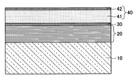
- FIG. 1 is a schematic cross-sectional view of a configuration example of a reflective mask blank according to an embodiment of the present invention.
- the reflective mask blank is configured by laminating a reflective layer 20, a protective layer 30, and an absorbing layer 40 in this order on a substrate 10.
- FIG. 2 is a schematic cross-sectional view of another configuration example of the reflective mask blank according to the embodiment of the present invention.
- the reflective mask blank is configured by laminating a reflective layer 20, a protective layer 30, a lower absorption layer 41, and an upper absorption layer 42 on a substrate 10 in this order.
- the absorption layer 40 is composed of two layers, a lower absorption layer 41 and an upper absorption layer 42.
- the substrate 10 preferably has a small coefficient of thermal expansion.
- the coefficient of thermal expansion of the substrate 10 is preferably 0 ⁇ 1.0 ⁇ 10 -7 / ° C., more preferably 0 ⁇ 0.3 ⁇ 10 -7 / ° C. at 20 ° C.
- SiO 2- TiO 2 glass As a material having a small coefficient of thermal expansion, for example, SiO 2- TiO 2 glass or the like can be used.
- the SiO 2 -TiO 2 type glass a SiO 2 90 ⁇ 95 wt%, it is preferable to use a quartz glass containing TiO 2 5 ⁇ 10% by weight.
- the coefficient of linear expansion near room temperature is substantially zero, and there is almost no dimensional change near room temperature.
- the SiO 2- TiO 2 system glass may contain trace components other than SiO 2 and TiO 2.
- the surface of the substrate 10 on which the reflective layer 20 is laminated (hereinafter referred to as "main surface") preferably has high smoothness.
- the smoothness of the main surface can be measured with an atomic force microscope and evaluated by the surface roughness.
- the surface roughness of the main surface is a root mean square roughness Rq, preferably 0.15 nm or less.
- the main surface is surface-processed so as to have a predetermined flatness. This is because the reflective mask obtains high pattern transfer accuracy and position accuracy.
- the flatness of the substrate 10 is preferably 100 nm or less, more preferably 50 nm or less, and further preferably 30 nm or less in a predetermined region (for example, a region of 132 mm ⁇ 132 mm) on the main surface.
- the substrate 10 has resistance to a cleaning liquid used for cleaning a reflective mask blank, a reflective mask blank after pattern formation, or a reflective mask.
- the substrate 10 preferably has high rigidity in order to prevent deformation of the film (reflection layer 20, etc.) formed on the substrate 10 due to film stress.
- the substrate 10 preferably has a high Young's modulus of 65 GPa or more.
- the reflective layer 20 has a high reflectance for EUV light. Specifically, when EUV light is incident on the surface of the reflective layer at an incident angle of 6 °, the maximum value of the reflectance of EUV light near a wavelength of 13.5 nm is preferably 60% or more, more preferably 65% or more. .. Similarly, even when the protective layer is laminated on the reflective layer, the maximum value of the reflectance of EUV light having a wavelength of around 13.5 nm is preferably 60% or more, more preferably 65% or more.
- the reflective layer 20 is preferably a multilayer reflective film in which a plurality of layers containing elements having different refractive indexes as main components with respect to EUV light are periodically laminated.
- the reflective layer is a multilayer reflective film.
- the multilayer reflective film may be laminated for a plurality of cycles with a laminated structure in which a high refractive index layer and a low refractive index layer are laminated in this order from the substrate 10 side as one cycle, or may be a low refractive index layer and a high refractive index layer. May be laminated in a plurality of cycles with the laminated structure in which the above is laminated in this order as one cycle.
- the high refractive index layer a layer containing Si can be used. By using a high refractive index layer containing Si, a reflective mask having excellent reflectance of EUV light can be obtained.
- a metal selected from the group consisting of Mo, Ru, Rh and Pt or an alloy thereof can be used. In the present embodiment, it is preferable that the low refractive index layer is a layer containing Mo and the high refractive index layer is a layer containing Si.
- the multilayer reflective film includes a plurality of high refractive index layers and a plurality of low refractive index layers, but the film thickness of the high refractive index layers or the film thickness of the low refractive index layers does not necessarily have to be the same.
- the film thickness and period of each layer constituting the multilayer reflective film can be appropriately selected depending on the film material used, the reflectance of EUV light required for the reflective layer, the wavelength of EUV light (exposure wavelength), and the like. For example, when the maximum value of the reflectance of EUV light having a wavelength of about 13.5 nm is 60% or more, the low refractive index layer (layer containing Mo) and the high refractive index layer (layer containing Si) are used. Mo / Si multilayer reflective films laminated alternately for 30 to 60 cycles are preferably used.
- Each layer constituting the multilayer reflective film can be formed into a desired thickness by using a known film forming method such as a magnetron sputtering method or an ion beam sputtering method.
- a known film forming method such as a magnetron sputtering method or an ion beam sputtering method.
- ion particles are supplied from an ion source to a target of a high refractive index material and a target of a low refractive index material.
- the protective layer 30 etches (usually dry-etches) the absorption layer 40 (lower absorption layer 41, upper absorption layer 42) to apply the absorber pattern 60 to the absorption layer 40 at the time of manufacturing the reflective mask shown in FIG. When formed, it protects the surface of the reflective layer 20 from damage due to etching. Further, the resist remaining on the reflective mask blank after etching is peeled off with a cleaning liquid to protect the reflective layer 20 from the cleaning liquid when cleaning the reflective mask blank. Therefore, the reflectance of the obtained reflective mask to EUV light is good.
- FIGS. 1 and 2 show the case where the protective layer 30 is one layer
- the protective layer 30 may be a plurality of layers.
- the material for forming the protective layer 30 a substance that is not easily damaged by etching when the absorbing layer 40 is etched is selected.
- one or more metals selected from the group consisting of elemental Ru metal, Ru, B, Si, Ti, Nb, Mo, Zr, Y, La, Co, and Re can be used.
- Ru metal and Ru alloy CrN and SiO 2 are preferable.
- the Ru metal simple substance and the Ru alloy are particularly preferable because they are difficult to be etched with respect to a gas containing no oxygen and function as an etching stopper during processing of the reflective mask.
- the film thickness of the protective layer 30 is not particularly limited as long as it can function as the protective layer 30.
- the film thickness of the protective layer 30 is preferably 1 to 8 nm, more preferably 1.5 to 6 nm, and even more preferably 2 to 5 nm from the viewpoint of maintaining the reflectance of the EUV light reflected by the reflective layer 20.
- a known film forming method such as a sputtering method or an ion beam sputtering method can be used.
- the absorption layer 40 preferably has characteristics such as a high absorption coefficient of EUV light, easy etching, and high cleaning resistance to a cleaning liquid for use in a reflective mask for EUV lithography.
- the absorption layer 40 absorbs EUV light, and the reflectance of EUV light is extremely low. However, if the reflectance of EUV light is too low, the phase shift effect is reduced. Therefore, when the surface of the absorption layer 40 is irradiated with EUV light, the reflectance of EUV light having a wavelength of around 13.53 nm is 2. It is 5 to 10%.
- the reflectance can be measured using an EUV reflectance meter for mask blanks (MBR, manufactured by AIXUV).
- the absorption layer 40 is processed by etching by dry etching using Cl-based gas or CF-based gas. Therefore, it is preferable that the absorption layer 40 can be easily etched.
- the absorption layer 40 is exposed to the cleaning liquid when the resist pattern remaining on the reflective mask blank after etching is removed by the cleaning liquid at the time of manufacturing the reflective mask described later.
- the cleaning liquid sulfuric acid hydrogen peroxide (SPM), sulfuric acid, ammonia, ammonia hydrogen peroxide (APM), OH radical cleaning water, ozone water and the like are used.
- a Ta-based material is preferably used as the material of the absorption layer 40.
- N, O, or B By adding N, O, or B to Ta, resistance to oxidation can be improved and stability over time can be improved.
- the absorption layer 40 is laminated with a two-layer structure, for example, a TaON film as a lower absorption layer 41 and a TaON film as an upper absorption layer 42. It is also preferable to have a structure in which the structure is formed.
- the absorption layer 40 in the present invention contains one or more elements selected from the group consisting of Ta, Nb, Mo, Ti, Zr, Re, Ru, Au, Pt, Pd, Rh, B, N, and O. It is preferable to contain it.
- the thin film can be thinned when used as a phase shift mask. Further, by adding Ta, N, O, and B to these materials, cleaning resistance and stability over time can be improved.
- the absorption layer 40 is preferably amorphous in crystal state. Thereby, the absorption layer 40 can have excellent smoothness and flatness. Further, by improving the smoothness and flatness of the absorbent layer 40, the edge roughness of the absorbent pattern 60 can be reduced during the production of the reflective mask shown in FIG. 9, and the dimensional accuracy of the absorbent pattern 60 can be improved. ..
- the absorption layer 40 is a single layer as in the reflective mask blank shown in FIG. 1, the number of steps during mask blank manufacturing can be reduced and the production efficiency can be improved.
- the absorption layer 40 is composed of two layers, the lower absorption layer 41 and the upper absorption layer 42, as in the reflective mask blank shown in FIG. 2, the optical constant and the film thickness of the upper absorption layer 42 are appropriately set. Therefore, it can be used as an antireflection film when inspecting the absorber pattern 60 using the inspection light at the time of manufacturing the reflective mask shown in FIG. Thereby, the inspection sensitivity at the time of inspection of the absorber pattern can be improved. Further, when a material containing oxygen is used for the upper absorption layer 42, cleaning resistance and stability are improved.
- the reflective mask blank of the present invention may have a hard mask layer on the absorption layer 40.
- the hard mask layer in the present invention preferably contains at least one element of Cr and Si.
- a material having high resistance to etching such as a Cr-based film containing Cr or a Si-based film containing Si, specifically, for dry etching using Cl-based gas or CF-based gas.
- a material with high resistance is used.
- the Cr-based film include Cr and a material obtained by adding O or N to Cr. Specific examples thereof include CrO, CrN, and CrON.
- the Si-based film include Si and a material obtained by adding one or more selected from the group consisting of O, N, C, and H to Si.
- the Si-based film is preferable because the side wall is unlikely to recede when the absorption layer 40 is dry-etched.
- dry etching can be performed even when the minimum line width of the absorber pattern 60 is reduced during the production of the reflective mask shown in FIG. Therefore, it is effective for miniaturization of the absorber pattern 60.
- the reflective mask blank of the present invention can be provided with a back surface conductive layer for an electrostatic chuck on a main surface (hereinafter, referred to as a back surface) opposite to the side on which the reflection layer 20 of the substrate 10 is laminated.
- the back surface conductive layer is required to have a low sheet resistance value as a characteristic.
- the sheet resistance value of the back surface conductive layer is, for example, 250 ⁇ / ⁇ or less, preferably 200 ⁇ / ⁇ or less.
- a metal such as Cr or Ta, or an alloy thereof can be used.
- a Cr compound containing one or more selected from the group consisting of B, N, O, and C in Cr can be used.
- a Ta compound containing one or more selected from the group consisting of B, N, O, and C in Ta can be used.
- the film thickness of the back surface conductive layer is not particularly limited as long as it satisfies the function for the electrostatic chuck, but is, for example, 10 to 400 nm.
- the back surface conductive layer can also be provided with stress adjustment on the back surface side of the reflective mask blank. That is, the back surface conductive layer can be adjusted so as to flatten the reflective mask blank by balancing the stress from various layers formed on the main surface side.
- a known film forming method such as a magnetron sputtering method or an ion beam sputtering method can be used.
- the back surface conductive layer can be formed on the back surface of the substrate, for example, before the reflection layer is formed.
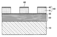
- FIG. 9 is a schematic cross-sectional view showing an example of the configuration of the reflective mask.
- the reflective mask shown in FIG. 9 has a desired absorber pattern 60 formed on the absorption layer 40 (lower absorption layer 41, upper absorption layer 42) of the reflection type mask blank shown in FIG.
- the absorber pattern is formed by a usual processing method, that is, resist coating, exposure, development, and etching on a reflective mask blank.
- an absorber pattern is formed in the single absorbent layer.
- Examples 1, 3 and 4 are examples, and example 2 is a comparative example.
- Example 1 As a substrate for film formation, a SiO 2- TiO 2 system glass substrate (outer shape: about 152 mm square, thickness: about 6.3 mm) was used. The coefficient of thermal expansion of the glass substrate is 0.02 ⁇ 10 -7 / ° C or less. The glass substrate was polished to process a smooth surface having a surface roughness of 0.15 nm or less in a root mean square roughness Rq and a flatness of 100 nm or less. A Cr layer having a thickness of about 100 nm was formed on the back surface of the glass substrate by using a magnetron sputtering method to form a back surface conductive layer for an electrostatic chuck. The sheet resistance value of the Cr layer was about 100 ⁇ / ⁇ .
- the Si film and the Mo film are alternately formed on the front surface of the substrate by an ion beam sputtering method for 40 cycles.
- the film thickness of the Si film is about 4.0 nm
- the film thickness of the Mo film is about 3.0 nm.
- a reflective layer multilayer reflective film having a total film thickness of about 280 nm ((Si film: 4.0 nm + Mo film: 3.0 nm) ⁇ 40) was formed.
- a Ru layer thickness: about 2.5 nm
- the reflectance at a wavelength of 13.53 nm was 64%.
- a TaNb film was formed as an absorption layer on the protective layer.
- XRR X-ray reflectivity method
- SmartLab HTP manufactured by Rigaku Co., Ltd.
- the relationship between the thickness of the absorbent layer of the reflective mask blank and the reflectance was measured.
- the reflectance was measured using an EUV reflectance meter for mask blanks (MBR, manufactured by AIXUV).
- the wavelength of EUV light was 13.53 nm.
- the relationship between the thickness of the absorbing layer and the reflectance is shown in FIG. 10 (a).
- the absorption layer has a peak reflectance of 3.2% near a film thickness of 72 nm. This reflectance satisfies the condition of 2.5% or more and 10% or less as a phase shift mask.
- FIG. 10A shows the simulation results together with the measured values.
- the refractive index n at a wavelength of 13.53 nm was 0.945
- the absorption coefficient k at the same wavelength was 0.0236.
- FIG. 10 (b) shows the reflected light spectrum when the film thickness is d MAX
- FIG. 10 (c) shows the reflected light spectrum when the film thickness is d MAX -6 nm. It can be seen that the measured values and the simulation results are in good agreement.
- the reflected light spectrum can be used to control the film thickness of the phase shift mask.
- Example 2 As the absorption layer, a TaN film was used instead of the TaNb film. If the refractive index n at a wavelength of 13.53nm 0.947, and 0.031 for the absorption coefficient k in the same wavelength, d MAX became 72.0nm than (4). The reflectance at this time is 1.2% from the simulation, and does not satisfy the condition of 2.5% or more and 10% or less as a phase shift mask. Regarding Examples 1 and 2, the simulation results when the isolated hole pattern of 22 nm on the wafer is exposed under the exposure conditions where the numerical aperture NA of the projection optical system is 0.33 and the ⁇ value is 0.5 are shown in FIGS. Shown in b). FIG.
- FIG. 11A shows the result of obtaining the film thickness dependence of NILS by simulation
- FIG. 11B shows the result of obtaining the film thickness dependence of the peak light intensity of the optical image by simulation.
- FIG. 11A it can be seen that in Example 2 in which the absorption layer is a TaN film, NILS is much smaller and the phase shift effect is smaller than in Example 1 in which the absorption layer is a TaNb film.
- FIG. 11B it can be seen that the peak light intensity at the time of exposure is lower in Example 2 in which the absorption layer is a TaN film than in Example 1 in which the absorption layer is a TaNb film.
- Example 3 As the absorption layer, a Re film was used instead of the TaNb film. If the refractive index n at a wavelength of 13.53nm 0.933, the absorption coefficient k in the same wavelength is 0.0405, d MAX is much thinner than Example 1 using the 44.8nm next, TaNb film from (4) .. This is because the n value is small. The reflectance at this time is 3.7% from the simulation, which satisfies the condition of 2.5% or more and 10% or less as a phase shift mask.
- Figures 12 (a) and 12 (b) show the simulation results when an isolated hole pattern of 22 nm is exposed on the wafer under the exposure conditions where the numerical aperture NA of the projection optical system is 0.33 and the ⁇ value is 0.5.
- FIG. 12 (a) shows the result of calculating the film thickness dependence of NILS by simulation
- FIG. 12 (b) shows the result of obtaining the film thickness dependence of the peak light intensity of the optical image by simulation.
- the NILS of Example 3 in which the Re film was used as the absorption layer had an absorption layer film thickness of around d MAX and d MAX -6 nm, as in Example 1 in which the TaNb film was used as the absorption layer.
- the light intensity of the optical image increases as the film thickness decreases.
- NILS reaches its maximum when the film thickness of the absorption layer is d MAX , and has a peak at d MAX -6 nm.
- the light intensity at the film thickness d MAX -6 nm is 6% higher than the light intensity at the film thickness d MAX.
- the optimum value of the film thickness of the absorption layer is either d MAX or d MAX -6 nm.
- Example 4 As the absorption layer, instead of the TaNb film, a TaNb film of the lower absorption layer and a two-layer film (TaNO (4 nm) / TaNb film) of the TaNO film (thickness 4 nm) of the upper absorption layer were used.
- the refractive index n 1 of TaNb as the lower absorption layer at a wavelength of 13.53 nm is 0.945
- the refractive index n 2 of TaON as the upper absorption layer at a wavelength of 13.53 nm is 0.968
- the absorption coefficient k 2 at the same wavelength is 0.968. If it is 0.0512, the d bi MAX is 71.6 nm from the equation (6).
- FIG. 12 (a) shows the simulation results when an isolated hole pattern of 22 nm is exposed on the wafer under the exposure conditions where the numerical aperture NA of the projection optical system is 0.33 and the ⁇ value is 0.5.
- the NILS of Example 4 using the TaNb film of the lower absorption layer and the TaNO film (thickness of 4 nm) of the upper absorption layer is an example of using the TaNb film as the absorption layer. Similar to No.
- the absorption layer film thickness has a peak near d bi MAX and d bi MAX -6 nm.
- the light intensity of the optical image increases as the film thickness decreases.
- NILS is maximized when the film thickness of the absorption layer is d bi MAX , and has a peak at d bi MAX -6 nm.
- the light intensity at the film thickness d bi MAX -6 nm is 6% higher than the light intensity at the film thickness d bi MAX.
- the optimum value of the film thickness of the absorption layer is either d bi MAX or d bi MAX -6 nm.
- FIGS. 13 (a) and 13 (b) show the reflected light spectra of the TaNb film, the Re film, and the TaON film (4 nm) / TaNb film described in Examples 1, 3 and 4.
- FIG. 13A shows a case where the film thickness is d MAX or d bi MAX , and the peak wavelength of the reflectance is around 13.53 nm.
- FIG. 13B shows a case where the film thickness is d MAX -6 nm or d bi MAX -6 nm, and the peak wavelength of the reflectance is around 13.63 nm.
- the peak wavelength of the reflected light can be used as a reference for controlling the film thickness of the absorbing layer, regardless of the film type.
- the present invention provides the following reflective mask blanks and reflective masks.
- a reflective mask blank having a reflective layer that reflects EUV light, a protective layer that protects the reflective layer, and an absorbing layer that absorbs EUV light on the substrate in this order.
- the reflectance of the absorption layer at a wavelength of 13.53 nm is 2.5 to 10%.
- the film thickness d of the absorption layer is A reflective mask blank characterized by satisfying the above relationship.
- the integer i is 0 or 1 and d MAX is Is.
- the refractive index of the absorption layer is n
- the absorption coefficient of the absorption layer is k.
- INT (x) is a function that returns an integer value with the decimal part truncated.
- a reflective mask blank having a reflective layer that reflects EUV light, a protective layer that protects the reflective layer, and an absorbing layer that absorbs EUV light on the substrate in this order.
- the reflectance of the absorption layer at a wavelength of 13.53 nm is 2.5 to 10%.
- the absorption layer is composed of two layers, a lower absorption layer and an upper absorption layer.
- the film thickness d bi of the absorption layer composed of the two layers is A reflective mask blank characterized by satisfying the above relationship. Where the integer i is 0 or 1 and d bi MAX is Is.
- the refractive index of the lower absorption layer is n 1
- the refractive index of the upper absorption layer is n 2
- the absorption coefficient of the upper absorption layer is k 2
- INT (x) is a function that returns an integer value with the decimal part truncated.
- the absorption layer contains one or more elements selected from the group consisting of Ta, Nb, Mo, Ti, Zr, Re, Ru, Au, Pt, Pd, Rh, B, N, and O.
- the reflective mask blank according to any one of (1) to (7) above which has a back surface conductive layer on the back surface of the substrate.
- Substrate 20 Reflective layer 30
- Protective layer 40 Absorbing layer 41
- Upper absorbing layer 60 Absorber pattern
Abstract
Description


反射光100と反射光200の位相の揃う条件は、二層からなる吸収層40の膜厚をdbiとして、反射面での位相のずれを考慮して下記(6)式で与えられ、NILSが最大値となる膜厚dbi MAXは、おおよそ下記(7)式となる。


これらの式をまとめると下記式となる。

The condition that the phases of the reflected
These formulas can be summarized as the following formulas.
吸収層の膜厚のより現実的な管理方法として、反射光のスペクトルを使用する方法が考えられる。反射光のスペクトルは市販の装置を使用して測定可能である。図8に吸収層の膜厚がdMAXおよびdMAX-6nmの際の反射光スペクトルを示す。ピーク波長λMAXは、それぞれ13.53nm、13.63nmとなっている。吸収層の膜厚管理の基準として、反射光のピーク波長λMAXを用いることができる。
この場合、ピーク波長λMAXが(13.53-0.1)nm≦λMAX≦(13.53+0.1)nm、あるいは(13.63-0.1)nm≦λMAX≦(13.63+0.1)nmを満たしていれば、位相シフト効果が大きく、かつ露光時のピーク光強度が高くなる。 (4) As can be seen from equation, d MAX is highly dependent on the refractive index n of the absorbing layer. As can be seen from Eq. (7), d bi MAX largely depends on the refractive index n 1 of the lower absorption layer and the refractive index n 2 of the upper absorption layer. However, it is difficult to frequently measure n, n 1 , and n 2 as a control during the production of mask blanks.
As a more realistic method for controlling the film thickness of the absorption layer, a method using a spectrum of reflected light can be considered. The spectrum of reflected light can be measured using a commercially available device. FIG. 8 shows the reflected light spectrum when the film thickness of the absorption layer is d MAX and d MAX -6 nm. The peak wavelength λ MAX is 13.53 nm and 13.63 nm, respectively. The peak wavelength λ MAX of the reflected light can be used as a reference for controlling the film thickness of the absorption layer.
In this case, the peak wavelength λ MAX is (13.53-0.1) nm ≤ λ MAX ≤ (13.53 + 0.1) nm, or (13.63-0.1) nm ≤ λ MAX ≤ (13.63 + 0). .1) If nm is satisfied, the phase shift effect is large and the peak light intensity at the time of exposure is high.
本発明の実施形態に係る反射型マスクブランクについて説明する。図1は、本発明の実施形態に係る反射型マスクブランクの一構成例の概略断面図である。図1に示すように、反射型マスクブランクは、基板10の上に、反射層20、保護層30、および吸収層40をこの順に積層して構成している。
図2は、本発明の実施形態に係る反射型マスクブランクの別の一構成例の概略断面図である。図2に示すように、反射型マスクブランクは、基板10の上に、反射層20、保護層30、下部吸収層41および上部吸収層42をこの順に積層して構成している。図2に示す反射型マスクブランクは、吸収層40が下部吸収層41と上部吸収層42の二層からなる。 <Reflective mask blank>
The reflective mask blank according to the embodiment of the present invention will be described. FIG. 1 is a schematic cross-sectional view of a configuration example of a reflective mask blank according to an embodiment of the present invention. As shown in FIG. 1, the reflective mask blank is configured by laminating a
FIG. 2 is a schematic cross-sectional view of another configuration example of the reflective mask blank according to the embodiment of the present invention. As shown in FIG. 2, the reflective mask blank is configured by laminating a
基板10は、熱膨張係数が小さいことが好ましい。基板10の熱膨張係数が小さい方が、EUV光による露光時の熱により吸収層40に形成されるパターンに歪みが生じるのを抑制できる。基板10の熱膨張係数は、具体的には、20℃において、0±1.0×10⁻⁷/℃が好ましく、0±0.3×10-7/℃がより好ましい。 (substrate)
The
反射層20は、EUV光に対して高い反射率を有する。具体的には、EUV光が入射角6°で反射層の表面に入射した際、波長13.5nm付近のEUV光の反射率の最大値は、60%以上が好ましく、65%以上がより好ましい。また、反射層の上に、保護層が積層されている場合でも、同様に、波長13.5nm付近のEUV光の反射率の最大値は、60%以上が好ましく、65%以上がより好ましい。 (Reflective layer)
The
多層反射膜を構成する各層の膜厚および周期は、使用する膜材料、反射層に要求されるEUV光の反射率またはEUV光の波長(露光波長)などにより適宜選択できる。例えば、反射層が波長13.5nm付近のEUV光の反射率の最大値を60%以上とする場合、低屈折率層(Moを含む層)と高屈折率層(Siを含む層)とを交互に30周期~60周期積層したMo/Si多層反射膜が好ましく用いられる。 The multilayer reflective film includes a plurality of high refractive index layers and a plurality of low refractive index layers, but the film thickness of the high refractive index layers or the film thickness of the low refractive index layers does not necessarily have to be the same.
The film thickness and period of each layer constituting the multilayer reflective film can be appropriately selected depending on the film material used, the reflectance of EUV light required for the reflective layer, the wavelength of EUV light (exposure wavelength), and the like. For example, when the maximum value of the reflectance of EUV light having a wavelength of about 13.5 nm is 60% or more, the low refractive index layer (layer containing Mo) and the high refractive index layer (layer containing Si) are used. Mo / Si multilayer reflective films laminated alternately for 30 to 60 cycles are preferably used.
保護層30は、図9に示す反射型マスクの製造時において、吸収層40(下部吸収層41、上部吸収層42)をエッチング(通常、ドライエッチング)して吸収層40に吸収体パターン60を形成する際、反射層20の表面をエッチングによるダメージから保護する。また、エッチング後の反射型マスクブランクに残っているレジストを洗浄液を用いて剥離して、反射型マスクブランクを洗浄する際に、反射層20を洗浄液から保護する。そのため、得られる反射型マスクのEUV光に対する反射率は良好となる。 (Protective layer)
The
保護層30を形成する材料としては、吸収層40のエッチングの際に、エッチングによる損傷を受け難い物質が選択される。この条件を満たす物質としては、例えば、Ru金属単体、Ruに、B、Si、Ti、Nb、Mo、Zr、Y、La、Co、およびReからなる群から選択される1種以上の金属を含有したRu合金、上記Ru合金に窒素を含む窒化物などのRu系材料;Cr、Al、Taおよびこれらに窒素を含む窒化物;SiO2、Si3N4、Al2O3またはこれらの混合物;などが例示される。これらの中でも、Ru金属単体およびRu合金、CrNおよびSiO2が好ましい。Ru金属単体およびRu合金は、酸素を含まないガスに対してエッチングされ難く、反射型マスクの加工時のエッチングストッパとして機能する点から、特に好ましい。 Although FIGS. 1 and 2 show the case where the
As the material for forming the
吸収層40は、EUVリソグラフィの反射型マスクに使用するためには、EUV光の吸収係数が高いこと、容易にエッチングできること、および洗浄液に対する洗浄耐性が高いことなどの特性を有することが好ましい。 (Absorption layer)
The
本発明の反射型マスクブランクは、吸収層40上にハードマスク層を備えていてもよい。本発明におけるハードマスク層は、CrおよびSiの少なくとも一方の元素を含むことが好ましい。ハードマスク層としては、Crを含むCr系膜、またはSiを含むSi系膜など、エッチングに対して耐性の高い材料、具体的には、Cl系ガスやCF系ガスを用いたドライエッチングに対して耐性の高い材料が用いられる。Cr系膜としては、例えば、Cr、およびCrにOまたはNを加えた材料などが挙げられる。具体的には、CrO、CrN、CrONが挙げられる。Si系膜としては、Si、並びにSiにO、N、C、およびHからなる群から選択される一種以上を加えた材料などが挙げられる。具体的には、SiO2、SiON、SiN、SiO、Si、SiC、SiCO、SiCN、SiCONが挙げられる。中でも、Si系膜は、吸収層40をドライエッチングする際に側壁の後退が生じ難いため好ましい。吸収層40上にハードマスク層を形成することで、図9に示す反射型マスクの製造時において、吸収体パターン60の最小線幅が小さくなっても、ドライエッチングを実施できる。そのため、吸収体パターン60の微細化に対して有効である。 (Other layers)
The reflective mask blank of the present invention may have a hard mask layer on the
次に、図2に示す反射型マスクブランクを用いて得られる反射型マスクについて説明する。図9は、反射型マスクの構成の一例を示す概略断面図である。図9に示す反射型マスクは、図2に示す反射型マスクブランクの吸収層40(下部吸収層41、上部吸収層42)に、所望の吸収体パターン60を形成したものである。吸収体パターンは通常の加工方法、すなわち反射型マスクブランク上へのレジスト塗布、露光、現像、エッチングにより形成される。なお、図1に示す反射型マスクブランクを用いて得られる反射型マスクの場合、単層の吸収層に吸収体パターンが形成される。 <Reflective mask>
Next, a reflective mask obtained by using the reflective mask blank shown in FIG. 2 will be described. FIG. 9 is a schematic cross-sectional view showing an example of the configuration of the reflective mask. The reflective mask shown in FIG. 9 has a desired
成膜用の基板として、SiO2-TiO2系のガラス基板(外形が約152mm角、厚さが約6.3mm)を使用した。なお、ガラス基板の熱膨張係数は0.02×10⁻⁷/℃以下である。ガラス基板を研磨して、表面粗さを二乗平均平方根粗さRqで0.15nm以下、平坦度を100nm以下の平滑な表面に加工した。ガラス基板の裏面上には、マグネトロンスパッタリング法を用いて、厚さが約100nmのCr層を成膜し、静電チャック用の裏面導電層を形成した。Cr層のシート抵抗値は100Ω/□程度であった。
基板の裏面に導電層を成膜した後、基板の表面にイオンビームスパッタリング法を用いて、Si膜およびMo膜を交互に成膜することを40周期繰り返す。Si膜の膜厚は、約4.0nmとし、Mo膜の膜厚は、約3.0nmとする。これにより、合計の膜厚が約280nm((Si膜:4.0nm+Mo膜:3.0nm)×40)の反射層(多層反射膜)を形成した。その後、反射層の上に、イオンビームスパッタリング法を用いてRu層(膜厚が約2.5nm)を成膜して、保護層を形成した。このとき、波長13.53nmにおける反射率は64%となった。
保護層上に、吸収層としてTaNb膜を成膜した。スパッタターゲットにはTaNb(Ta:Nb=60:40)を用い、スパッタガスにはArを用いた。吸収層のスパッタ時にステージの回転を止めることにより、面内で膜厚分布を有する吸収層を得た。これにより、図1に示す反射型マスクブランクを作製した。吸収層の膜厚は、X線回折装置(株式会社リガク社製、SmartLab HTP)を用いてX線反射率法(XRR)にて測定した。
反射型マスクブランクの吸収層の厚さと反射率の関係を測定した。反射率の測定には、マスクブランク用EUV反射率計(AIXUV社製、MBR)を用いて行った。EUV光の波長は13.53nmとした。吸収層の厚さと反射率との関係を図10(a)に示す。吸収層の膜厚72nm付近で反射率3.2%のピークを持っている。この反射率は位相シフトマスクとしての条件である2.5%以上、10%以下を満たしている。
図10(a)には、実測値とともにシミュレーション結果を示している。シミュレーションでは、波長13.53nmにおける屈折率nを0.945とし、同波長における吸収係数kを0.0236とした。実測値とシミュレーション結果は良く一致していることが判る。
上記の条件では、(4)式よりdMAXは72.3nmとなる。図10(b)には膜厚がdMAXでの反射光スペクトル、図10(c)には膜厚がdMAX-6nmでの反射光スペクトルを示す。実測値とシミュレーション結果は良く一致していることが判る。位相シフトマスクの膜厚管理に反射光スペクトルを用いることができる。 [Example 1]
As a substrate for film formation, a SiO 2- TiO 2 system glass substrate (outer shape: about 152 mm square, thickness: about 6.3 mm) was used. The coefficient of thermal expansion of the glass substrate is 0.02 × 10 -7 / ° C or less. The glass substrate was polished to process a smooth surface having a surface roughness of 0.15 nm or less in a root mean square roughness Rq and a flatness of 100 nm or less. A Cr layer having a thickness of about 100 nm was formed on the back surface of the glass substrate by using a magnetron sputtering method to form a back surface conductive layer for an electrostatic chuck. The sheet resistance value of the Cr layer was about 100Ω / □.
After forming a conductive layer on the back surface of the substrate, the Si film and the Mo film are alternately formed on the front surface of the substrate by an ion beam sputtering method for 40 cycles. The film thickness of the Si film is about 4.0 nm, and the film thickness of the Mo film is about 3.0 nm. As a result, a reflective layer (multilayer reflective film) having a total film thickness of about 280 nm ((Si film: 4.0 nm + Mo film: 3.0 nm) × 40) was formed. Then, a Ru layer (thickness: about 2.5 nm) was formed on the reflective layer by using an ion beam sputtering method to form a protective layer. At this time, the reflectance at a wavelength of 13.53 nm was 64%.
A TaNb film was formed as an absorption layer on the protective layer. TaNb (Ta: Nb = 60: 40) was used as the sputtering target, and Ar was used as the sputtering gas. By stopping the rotation of the stage during sputtering of the absorption layer, an absorption layer having an in-plane film thickness distribution was obtained. As a result, the reflective mask blank shown in FIG. 1 was produced. The film thickness of the absorption layer was measured by the X-ray reflectivity method (XRR) using an X-ray diffractometer (SmartLab HTP, manufactured by Rigaku Co., Ltd.).
The relationship between the thickness of the absorbent layer of the reflective mask blank and the reflectance was measured. The reflectance was measured using an EUV reflectance meter for mask blanks (MBR, manufactured by AIXUV). The wavelength of EUV light was 13.53 nm. The relationship between the thickness of the absorbing layer and the reflectance is shown in FIG. 10 (a). The absorption layer has a peak reflectance of 3.2% near a film thickness of 72 nm. This reflectance satisfies the condition of 2.5% or more and 10% or less as a phase shift mask.
FIG. 10A shows the simulation results together with the measured values. In the simulation, the refractive index n at a wavelength of 13.53 nm was 0.945, and the absorption coefficient k at the same wavelength was 0.0236. It can be seen that the measured values and the simulation results are in good agreement.
In the above conditions, d MAX is the 72.3nm than (4). FIG. 10 (b) shows the reflected light spectrum when the film thickness is d MAX , and FIG. 10 (c) shows the reflected light spectrum when the film thickness is d MAX -6 nm. It can be seen that the measured values and the simulation results are in good agreement. The reflected light spectrum can be used to control the film thickness of the phase shift mask.
吸収層として、TaNb膜の代わりにTaN膜を用いた。波長13.53nmにおける屈折率nを0.947、同波長における吸収係数kを0.031とすると、dMAXは(4)式より72.0nmとなった。このときの反射率はシミュレーションより1.2%となり、位相シフトマスクとしての条件である2.5%以上、10%以下を満たしていない。
例1,2について、投影光学系の開口数NAが0.33、σ値が0.5の露光条件でウエハ上22nmの孤立ホールパターンを露光した場合のシミュレーション結果を図11(a),(b)に示す。図11(a)にNILSの膜厚依存性をシミュレーションにより求めた結果を示し、図11(b)に光学像のピーク光強度の膜厚依存性をシミュレーションにより求めた結果を示す。図11(a),(b)では、横軸を吸収層の膜厚と、(4)式より求まるdMAXとの差としている。図11(a)に示すように、吸収層がTaNb膜の例1に比べ、吸収層がTaN膜の例2は、NILSはずっと小さくなり、位相シフト効果は小さいことが判る。図11(b)に示すように、吸収層がTaNb膜の例1に比べ、吸収層がTaN膜の例2は、露光時のピーク光強度が低いことが判る。 [Example 2]
As the absorption layer, a TaN film was used instead of the TaNb film. If the refractive index n at a wavelength of 13.53nm 0.947, and 0.031 for the absorption coefficient k in the same wavelength, d MAX became 72.0nm than (4). The reflectance at this time is 1.2% from the simulation, and does not satisfy the condition of 2.5% or more and 10% or less as a phase shift mask.
Regarding Examples 1 and 2, the simulation results when the isolated hole pattern of 22 nm on the wafer is exposed under the exposure conditions where the numerical aperture NA of the projection optical system is 0.33 and the σ value is 0.5 are shown in FIGS. Shown in b). FIG. 11A shows the result of obtaining the film thickness dependence of NILS by simulation, and FIG. 11B shows the result of obtaining the film thickness dependence of the peak light intensity of the optical image by simulation. FIG. 11 (a), the (b), the horizontal axis and the thickness of the absorbing layer, and a difference between the d MAX which is obtained from equation (4). As shown in FIG. 11A, it can be seen that in Example 2 in which the absorption layer is a TaN film, NILS is much smaller and the phase shift effect is smaller than in Example 1 in which the absorption layer is a TaNb film. As shown in FIG. 11B, it can be seen that the peak light intensity at the time of exposure is lower in Example 2 in which the absorption layer is a TaN film than in Example 1 in which the absorption layer is a TaNb film.
吸収層として、TaNb膜の代わりにRe膜を用いた。波長13.53nmにおける屈折率nを0.933、同波長における吸収係数kを0.0405とすると、dMAXは(4)式より44.8nmとなり、TaNb膜を用いた例1よりずっと薄くなる。これはn値が小さいためである。このときの反射率はシミュレーションより3.7%となり、位相シフトマスクとしての条件である2.5%以上、10%以下を満たしている。投影光学系の開口数NAが0.33、σ値が0.5の露光条件でウエハ上に22nmの孤立ホールパターンを露光した場合のシミュレーション結果を図12(a),(b)に示す。図12(a)にNILSの膜厚依存性をシミュレーションにより求めた結果を示し、図12(b)に光学像のピーク光強度の膜厚依存性をシミュレーションにより求めた結果を示す。図12(a),(b)では、横軸を吸収層の膜厚と、(4)式より求まるdMAXとの差としている。図12(a)に示すように、吸収層としてRe膜を用いた例3のNILSは、吸収層としてTaNb膜を用いた例1と同じく、吸収層膜厚がdMAX、dMAX-6nm付近でピークを持っている。
図12(b)より判るように、光学像の光強度は膜厚が薄いほど大きくなる。一方、NILSは、吸収層の膜厚がdMAXのとき最大になり、dMAX-6nmにもピークを持っている。膜厚dMAX-6nmでの光強度は、膜厚dMAXでの光強度より6%高い。NILSと光強度のバランスを考慮すると、吸収層の膜厚の最適値はdMAXあるいはdMAX-6nmのどちらかになる。 [Example 3]
As the absorption layer, a Re film was used instead of the TaNb film. If the refractive index n at a wavelength of 13.53nm 0.933, the absorption coefficient k in the same wavelength is 0.0405, d MAX is much thinner than Example 1 using the 44.8nm next, TaNb film from (4) .. This is because the n value is small. The reflectance at this time is 3.7% from the simulation, which satisfies the condition of 2.5% or more and 10% or less as a phase shift mask. Figures 12 (a) and 12 (b) show the simulation results when an isolated hole pattern of 22 nm is exposed on the wafer under the exposure conditions where the numerical aperture NA of the projection optical system is 0.33 and the σ value is 0.5. FIG. 12 (a) shows the result of calculating the film thickness dependence of NILS by simulation, and FIG. 12 (b) shows the result of obtaining the film thickness dependence of the peak light intensity of the optical image by simulation. FIG. 12 (a), the (b), the horizontal axis and the thickness of the absorbing layer, and a difference between the d MAX which is obtained from equation (4). As shown in FIG. 12 (a), the NILS of Example 3 in which the Re film was used as the absorption layer had an absorption layer film thickness of around d MAX and d MAX -6 nm, as in Example 1 in which the TaNb film was used as the absorption layer. Has a peak at.
As can be seen from FIG. 12B, the light intensity of the optical image increases as the film thickness decreases. On the other hand, NILS reaches its maximum when the film thickness of the absorption layer is d MAX , and has a peak at d MAX -6 nm. The light intensity at the film thickness d MAX -6 nm is 6% higher than the light intensity at the film thickness d MAX. Considering the balance between NILS and light intensity, the optimum value of the film thickness of the absorption layer is either d MAX or d MAX -6 nm.
吸収層として、TaNb膜の代わりに、下部吸収層のTaNb膜、上部吸収層のTaNO膜(膜厚4nm)の二層膜(TaNO(4nm)/TaNb膜)を用いた。下部吸収層としてのTaNbの波長13.53nmにおける屈折率n1は0.945、上部吸収層としてのTaONの波長13.53nmにおける屈折率n2は0.968、同波長における吸収係数k2は0.0512とすると、dbi MAXは(6)式より71.6nmとなる。このときの反射率はシミュレーションより3.5%となり、位相シフトマスクとして十分な効果を期待できる。TaNO膜が最表面にあるため、TaNb単膜に比べ洗浄に強く、経時安定性良好になる。投影光学系の開口数NAが0.33、σ値が0.5の露光条件でウエハ上に22nmの孤立ホールパターンを露光した場合のシミュレーション結果を図12(a),(b)に示す。図12(a)に示すように、下部吸収層のTaNb膜、上部吸収層のTaNO膜(膜厚4nm)の二層膜を用いた例4のNILSは、吸収層としてTaNb膜を用いた例1と同じく、吸収層膜厚がdbi MAX、dbi MAX-6nm付近でピークを持っている。
図12(b)より判るように、光学像の光強度は膜厚が薄いほど大きくなる。一方、NILSは、吸収層の膜厚がdbi MAXのとき最大になり、dbi MAX-6nmにもピークを持っている。膜厚dbi MAX-6nmでの光強度は、膜厚dbi MAXでの光強度より6%高い。NILSと光強度のバランスを考慮すると、吸収層の膜厚の最適値はdbi MAXあるいはdbi MAX-6nmのどちらかになる。 [Example 4]
As the absorption layer, instead of the TaNb film, a TaNb film of the lower absorption layer and a two-layer film (TaNO (4 nm) / TaNb film) of the TaNO film (
As can be seen from FIG. 12B, the light intensity of the optical image increases as the film thickness decreases. On the other hand, NILS is maximized when the film thickness of the absorption layer is d bi MAX , and has a peak at d bi MAX -6 nm. The light intensity at the film thickness d bi MAX -6 nm is 6% higher than the light intensity at the film thickness d bi MAX. Considering the balance between NILS and light intensity, the optimum value of the film thickness of the absorption layer is either d bi MAX or d bi MAX -6 nm.
(1)基板上に、EUV光を反射する反射層と、前記反射層を保護する保護層と、EUV光を吸収する吸収層をこの順に有する反射型マスクブランクであって、
前記吸収層の波長13.53nmにおける反射率が2.5~10%であり、
前記吸収層の膜厚dは

ここで、整数iは0または1であり、dMAXは

(2)基板上に、EUV光を反射する反射層と、前記反射層を保護する保護層と、EUV光を吸収する吸収層をこの順に有する反射型マスクブランクであって、
前記吸収層の波長13.53nmにおける反射率が2.5~10%であり、
前記吸収層が、下部吸収層および上部吸収層の二層からなり、
前記二層からなる吸収層の膜厚dbiは

ここで、整数iは0または1であり、dbi MAXは

(3)前記反射層の波長13.53nmにおける反射光に対する前記吸収層の波長13.53nmにおける反射光の位相差は190~220度であることを特徴とする上記(1)または(2)に記載の反射型マスクブランク。
(4)前記吸収層はTa、Nb、Mo、Ti、Zr、Re、Ru、Au、Pt、Pd、Rh、B、N、および、Oからなる群から選択される1種以上の元素を含有することを特徴とする上記(1)~(3)のいずれか一つに記載の反射型マスクブランク。
(5)前記吸収層の反射光スペクトルのピーク波長をλMAXとしたとき、前記整数iに対応して

(6)前記吸収層の上にハードマスク層を有することを特徴とする上記(1)~(5)のいずれか一つに記載の反射型マスクブランク。
(7)前記ハードマスク層は、CrおよびSiの少なくとも一方の元素を含むことを特徴とする上記(6)に記載の反射型マスクブランク。
(8)前記基板の裏面に裏面導電層を有することを特徴とする上記(1)~(7)のいずれか一つに記載の反射型マスクブランク。
(9)前記裏面導電層の材料は、CrもしくはTa、またはこれらの合金であることを特徴とする上記(8)に記載の反射型マスクブランク。
(10)上記(1)~(9)のいずれか一つに記載の反射型マスクブランクの前記吸収層に、パターンが形成されている反射型マスク。 As described above, the present invention provides the following reflective mask blanks and reflective masks.
(1) A reflective mask blank having a reflective layer that reflects EUV light, a protective layer that protects the reflective layer, and an absorbing layer that absorbs EUV light on the substrate in this order.
The reflectance of the absorption layer at a wavelength of 13.53 nm is 2.5 to 10%.
The film thickness d of the absorption layer is
Where the integer i is 0 or 1 and d MAX is
(2) A reflective mask blank having a reflective layer that reflects EUV light, a protective layer that protects the reflective layer, and an absorbing layer that absorbs EUV light on the substrate in this order.
The reflectance of the absorption layer at a wavelength of 13.53 nm is 2.5 to 10%.
The absorption layer is composed of two layers, a lower absorption layer and an upper absorption layer.
The film thickness d bi of the absorption layer composed of the two layers is
Where the integer i is 0 or 1 and d bi MAX is
(3) The above (1) or (2), wherein the phase difference of the reflected light at the wavelength of 13.53 nm of the absorbing layer with respect to the reflected light at the wavelength of 13.53 nm of the reflecting layer is 190 to 220 degrees. The reflective mask blank described.
(4) The absorption layer contains one or more elements selected from the group consisting of Ta, Nb, Mo, Ti, Zr, Re, Ru, Au, Pt, Pd, Rh, B, N, and O. The reflective mask blank according to any one of (1) to (3) above.
(5) When the peak wavelength of the reflected light spectrum of the absorption layer is λ MAX , it corresponds to the integer i.
(6) The reflective mask blank according to any one of (1) to (5) above, which has a hard mask layer on the absorption layer.
(7) The reflective mask blank according to (6) above, wherein the hard mask layer contains at least one element of Cr and Si.
(8) The reflective mask blank according to any one of (1) to (7) above, which has a back surface conductive layer on the back surface of the substrate.
(9) The reflective mask blank according to (8) above, wherein the material of the back surface conductive layer is Cr, Ta, or an alloy thereof.
(10) A reflective mask in which a pattern is formed on the absorption layer of the reflective mask blank according to any one of (1) to (9) above.
本出願は、2019年10月29日出願の日本特許出願2019-195856に基づくものであり、その内容はここに参照として取り込まれる。 Although the embodiments have been described above, the above-described embodiments are presented as examples, and the present invention is not limited to the above-described embodiments. The above-described embodiment can be implemented in various other forms, and various combinations, omissions, replacements, changes, etc. can be made without departing from the gist of the invention. These embodiments and modifications thereof are included in the scope and gist of the invention, and are also included in the scope of the invention described in the claims and the equivalent scope thereof.
This application is based on Japanese Patent Application 2019-195856 filed on October 29, 2019, the contents of which are incorporated herein by reference.
20 反射層
30 保護層
40 吸収層
41 下部吸収層
42 上部吸収層
60 吸収体パターン 10
Claims (10)
- 基板上に、EUV光を反射する反射層と、前記反射層を保護する保護層と、EUV光を吸収する吸収層をこの順に有する反射型マスクブランクであって、
前記吸収層の波長13.53nmにおける反射率が2.5~10%であり、
前記吸収層の膜厚dは

ここで、整数iは0または1であり、dMAXは

The reflectance of the absorption layer at a wavelength of 13.53 nm is 2.5 to 10%.
The film thickness d of the absorption layer is
Where the integer i is 0 or 1 and d MAX is
- 基板上に、EUV光を反射する反射層と、前記反射層を保護する保護層と、EUV光を吸収する吸収層をこの順に有する反射型マスクブランクであって、
前記吸収層の波長13.53nmにおける反射率が2.5~10%であり、
前記吸収層が、下部吸収層および上部吸収層の二層からなり、
前記二層からなる吸収層の膜厚dbiは

ここで、整数iは0または1であり、dbi MAXは

The reflectance of the absorption layer at a wavelength of 13.53 nm is 2.5 to 10%.
The absorption layer is composed of two layers, a lower absorption layer and an upper absorption layer.
The film thickness d bi of the absorption layer composed of the two layers is
Where the integer i is 0 or 1 and d bi MAX is
- 前記反射層の波長13.53nmにおける反射光に対する前記吸収層の波長13.53nmにおける反射光の位相差は190~220度であることを特徴とする請求項1または2に記載の反射型マスクブランク。 The reflective mask blank according to claim 1 or 2, wherein the phase difference of the reflected light of the absorbing layer at a wavelength of 13.53 nm with respect to the reflected light of the reflecting layer at a wavelength of 13.53 nm is 190 to 220 degrees. ..
- 前記吸収層はTa、Nb、Mo、Ti、Zr、Re、Ru、Au、Pt、Pd、Rh、B、N、および、Oからなる群から選択される1種以上の元素を含有することを特徴とする請求項1~3のいずれか一項に記載の反射型マスクブランク。 The absorption layer contains one or more elements selected from the group consisting of Ta, Nb, Mo, Ti, Zr, Re, Ru, Au, Pt, Pd, Rh, B, N, and O. The reflective mask blank according to any one of claims 1 to 3, wherein the reflective mask blank is characterized.
- 前記吸収層の反射光スペクトルのピーク波長をλMAXとしたとき、前記整数iに対応して

- 前記吸収層の上にハードマスク層を有することを特徴とする請求項1~5のいずれか一項に記載の反射型マスクブランク。 The reflective mask blank according to any one of claims 1 to 5, wherein a hard mask layer is provided on the absorption layer.
- 前記ハードマスク層は、CrおよびSiの少なくとも一方の元素を含むことを特徴とする請求項6に記載の反射型マスクブランク。 The reflective mask blank according to claim 6, wherein the hard mask layer contains at least one element of Cr and Si.
- 前記基板の裏面に裏面導電層を有することを特徴とする請求項1~7のいずれか一項に記載の反射型マスクブランク。 The reflective mask blank according to any one of claims 1 to 7, wherein the back surface conductive layer is provided on the back surface of the substrate.
- 前記裏面導電層の材料は、CrもしくはTa、またはこれらの合金であることを特徴とする請求項8に記載の反射型マスクブランク。 The reflective mask blank according to claim 8, wherein the material of the back surface conductive layer is Cr, Ta, or an alloy thereof.
- 請求項1~9のいずれか一項に記載の反射型マスクブランクの前記吸収層に、パターンが形成されている反射型マスク。 A reflective mask in which a pattern is formed on the absorption layer of the reflective mask blank according to any one of claims 1 to 9.
Priority Applications (5)
| Application Number | Priority Date | Filing Date | Title |
|---|---|---|---|
| KR1020247006841A KR20240033148A (en) | 2019-10-29 | 2020-10-26 | Reflective mask blank and reflective mask |
| KR1020227013985A KR102644109B1 (en) | 2019-10-29 | 2020-10-26 | Reflective mask blanks and reflective masks |
| JP2021553606A JP7363913B2 (en) | 2019-10-29 | 2020-10-26 | Reflective mask blanks and reflective masks |
| US17/658,763 US11914283B2 (en) | 2019-10-29 | 2022-04-11 | Reflective mask blank and reflective mask |
| JP2023162137A JP2023175863A (en) | 2019-10-29 | 2023-09-26 | Reflection type mask blank and reflection type mask |
Applications Claiming Priority (2)
| Application Number | Priority Date | Filing Date | Title |
|---|---|---|---|
| JP2019-195856 | 2019-10-29 | ||
| JP2019195856 | 2019-10-29 |
Related Child Applications (1)
| Application Number | Title | Priority Date | Filing Date |
|---|---|---|---|
| US17/658,763 Continuation US11914283B2 (en) | 2019-10-29 | 2022-04-11 | Reflective mask blank and reflective mask |
Publications (1)
| Publication Number | Publication Date |
|---|---|
| WO2021085382A1 true WO2021085382A1 (en) | 2021-05-06 |
Family
ID=75715949
Family Applications (1)
| Application Number | Title | Priority Date | Filing Date |
|---|---|---|---|
| PCT/JP2020/040115 WO2021085382A1 (en) | 2019-10-29 | 2020-10-26 | Reflective mask blank and reflective mask |
Country Status (4)
| Country | Link |
|---|---|
| US (1) | US11914283B2 (en) |
| JP (2) | JP7363913B2 (en) |
| KR (2) | KR20240033148A (en) |
| WO (1) | WO2021085382A1 (en) |
Cited By (2)
| Publication number | Priority date | Publication date | Assignee | Title |
|---|---|---|---|---|
| WO2023095769A1 (en) * | 2021-11-24 | 2023-06-01 | 株式会社トッパンフォトマスク | Reflective photomask blank and reflective photomask |
| WO2024029409A1 (en) * | 2022-08-03 | 2024-02-08 | Agc株式会社 | Reflective mask blank and reflective mask |
Citations (6)
| Publication number | Priority date | Publication date | Assignee | Title |
|---|---|---|---|---|
| JPH07114173A (en) * | 1993-10-15 | 1995-05-02 | Canon Inc | Reflection mask for lithography and reduction stepper |
| JP2010067757A (en) * | 2008-09-10 | 2010-03-25 | Toppan Printing Co Ltd | Halftone-type euv mask, halftone-type euv mask blank, production method of halftone-type euv mask, and pattern transfer method |
| WO2017090485A1 (en) * | 2015-11-27 | 2017-06-01 | Hoya株式会社 | Substrate for mask blank, substrate with attached multilayer reflection film, reflective mask blank, reflective mask, and method for manufacturing semiconductor device |
| WO2018135467A1 (en) * | 2017-01-17 | 2018-07-26 | Hoya株式会社 | Reflective mask blank, reflective mask, method for producing same, and method for producing semiconductor device |
| WO2018159392A1 (en) * | 2017-03-03 | 2018-09-07 | Hoya株式会社 | Reflective mask blank, reflective mask, and semiconductor device production method |
| JP2018141969A (en) * | 2017-02-27 | 2018-09-13 | Hoya株式会社 | Mask blank, method for manufacturing transfer mask, and method for manufacturing semiconductor device |
Family Cites Families (9)
| Publication number | Priority date | Publication date | Assignee | Title |
|---|---|---|---|---|
| JPS5266988U (en) | 1975-11-13 | 1977-05-18 | ||
| JP4780847B2 (en) | 2001-03-21 | 2011-09-28 | Hoya株式会社 | Reflective mask blank for EUV exposure and reflective mask for EUV exposure |
| US7390596B2 (en) | 2002-04-11 | 2008-06-24 | Hoya Corporation | Reflection type mask blank and reflection type mask and production methods for them |
| JP4163038B2 (en) | 2002-04-15 | 2008-10-08 | Hoya株式会社 | Reflective mask blank, reflective mask, and semiconductor manufacturing method |
| JP4703353B2 (en) | 2005-10-14 | 2011-06-15 | Hoya株式会社 | SUBSTRATE WITH MULTILAYER REFLECTIVE FILM, ITS MANUFACTURING METHOD, REFLECTIVE MASK BLANK AND REFLECTIVE MASK |
| JP6861095B2 (en) * | 2017-03-03 | 2021-04-21 | Hoya株式会社 | Method for manufacturing reflective mask blanks, reflective masks and semiconductor devices |
| JP7063075B2 (en) * | 2017-04-17 | 2022-05-09 | Agc株式会社 | Reflective mask blank for EUV exposure and reflective mask |
| KR20200018476A (en) | 2017-07-05 | 2020-02-19 | 도판 인사츠 가부시키가이샤 | Reflective Photomask Blanks and Reflective Photomasks |
| US10890842B2 (en) * | 2017-09-21 | 2021-01-12 | AGC Inc. | Reflective mask blank, reflective mask, and process for producing reflective mask blank |
-
2020
- 2020-10-26 KR KR1020247006841A patent/KR20240033148A/en active Application Filing
- 2020-10-26 WO PCT/JP2020/040115 patent/WO2021085382A1/en active Application Filing
- 2020-10-26 KR KR1020227013985A patent/KR102644109B1/en active IP Right Grant
- 2020-10-26 JP JP2021553606A patent/JP7363913B2/en active Active
-
2022
- 2022-04-11 US US17/658,763 patent/US11914283B2/en active Active
-
2023
- 2023-09-26 JP JP2023162137A patent/JP2023175863A/en active Pending
Patent Citations (6)
| Publication number | Priority date | Publication date | Assignee | Title |
|---|---|---|---|---|
| JPH07114173A (en) * | 1993-10-15 | 1995-05-02 | Canon Inc | Reflection mask for lithography and reduction stepper |
| JP2010067757A (en) * | 2008-09-10 | 2010-03-25 | Toppan Printing Co Ltd | Halftone-type euv mask, halftone-type euv mask blank, production method of halftone-type euv mask, and pattern transfer method |
| WO2017090485A1 (en) * | 2015-11-27 | 2017-06-01 | Hoya株式会社 | Substrate for mask blank, substrate with attached multilayer reflection film, reflective mask blank, reflective mask, and method for manufacturing semiconductor device |
| WO2018135467A1 (en) * | 2017-01-17 | 2018-07-26 | Hoya株式会社 | Reflective mask blank, reflective mask, method for producing same, and method for producing semiconductor device |
| JP2018141969A (en) * | 2017-02-27 | 2018-09-13 | Hoya株式会社 | Mask blank, method for manufacturing transfer mask, and method for manufacturing semiconductor device |
| WO2018159392A1 (en) * | 2017-03-03 | 2018-09-07 | Hoya株式会社 | Reflective mask blank, reflective mask, and semiconductor device production method |
Cited By (2)
| Publication number | Priority date | Publication date | Assignee | Title |
|---|---|---|---|---|
| WO2023095769A1 (en) * | 2021-11-24 | 2023-06-01 | 株式会社トッパンフォトマスク | Reflective photomask blank and reflective photomask |
| WO2024029409A1 (en) * | 2022-08-03 | 2024-02-08 | Agc株式会社 | Reflective mask blank and reflective mask |
Also Published As
| Publication number | Publication date |
|---|---|
| JP2023175863A (en) | 2023-12-12 |
| KR102644109B1 (en) | 2024-03-07 |
| JPWO2021085382A1 (en) | 2021-05-06 |
| US11914283B2 (en) | 2024-02-27 |
| KR20240033148A (en) | 2024-03-12 |
| JP7363913B2 (en) | 2023-10-18 |
| TW202121048A (en) | 2021-06-01 |
| KR20220086585A (en) | 2022-06-23 |
| US20220236636A1 (en) | 2022-07-28 |
Similar Documents
| Publication | Publication Date | Title |
|---|---|---|
| KR101981897B1 (en) | Reflective mask blank, reflective mask, and process for producing reflective mask blank | |
| US8288062B2 (en) | Reflective mask blank for EUV lithography | |
| US8828627B2 (en) | Reflective mask blank for EUV lithography and reflective mask for EUV lithography | |
| US8081384B2 (en) | Multilayer reflective film coated substrate, manufacturing method thereof, reflective mask blank, and reflective mask | |
| US8546047B2 (en) | Reflective mask blank and method of manufacturing a reflective mask | |
| US8329361B2 (en) | Reflective mask blank, method of manufacturing a reflective mask blank and method of manufacturing a reflective mask | |
| US8927181B2 (en) | Reflective mask blank for EUV lithography | |
| JP5348141B2 (en) | Reflective mask blank for EUV lithography | |
| US7804648B2 (en) | Multilayer reflective film coated substrate, manufacturing method thereof, reflective mask blank, and reflective mask | |
| JP6965833B2 (en) | Manufacturing method of reflective mask blank, reflective mask and reflective mask blank | |
| JP2023175863A (en) | Reflection type mask blank and reflection type mask | |
| WO2022050156A1 (en) | Reflection-type mask, reflection-type mask blank, and method for manufacturing reflection-type mask | |
| US20210349387A1 (en) | Reflective mask blank, reflective mask, and process for producing reflective mask blank | |
| US20220187699A1 (en) | Reflective mask blank for euvl, reflective mask for euvl, and method of manufacturing reflective mask for euvl | |
| JP5333016B2 (en) | Reflective mask blank for EUV lithography | |
| TWI830961B (en) | Reflective photomask base and reflective photomask | |
| WO2022249863A1 (en) | Mask blank, reflective mask, and method for producing semiconductor device | |
| TW202331406A (en) | Reflection-type mask blank, reflection-type mask, and method for producing reflection-type mask | |
| JP2022093271A (en) | Reflective mask blank for euvl, reflective mask for euvl, and method of manufacturing reflective mask for euvl |
Legal Events
| Date | Code | Title | Description |
|---|---|---|---|
| 121 | Ep: the epo has been informed by wipo that ep was designated in this application |
Ref document number: 20882063 Country of ref document: EP Kind code of ref document: A1 |
|
| ENP | Entry into the national phase |
Ref document number: 2021553606 Country of ref document: JP Kind code of ref document: A |
|
| ENP | Entry into the national phase |
Ref document number: 20227013985 Country of ref document: KR Kind code of ref document: A |
|
| NENP | Non-entry into the national phase |
Ref country code: DE |
|
| 122 | Ep: pct application non-entry in european phase |
Ref document number: 20882063 Country of ref document: EP Kind code of ref document: A1 |