WO2021084717A1 - 情報処理回路および情報処理回路の設計方法 - Google Patents
情報処理回路および情報処理回路の設計方法 Download PDFInfo
- Publication number
- WO2021084717A1 WO2021084717A1 PCT/JP2019/042927 JP2019042927W WO2021084717A1 WO 2021084717 A1 WO2021084717 A1 WO 2021084717A1 JP 2019042927 W JP2019042927 W JP 2019042927W WO 2021084717 A1 WO2021084717 A1 WO 2021084717A1
- Authority
- WO
- WIPO (PCT)
- Prior art keywords
- circuit
- information processing
- processing circuit
- layer
- parameter
- Prior art date
- Legal status (The legal status is an assumption and is not a legal conclusion. Google has not performed a legal analysis and makes no representation as to the accuracy of the status listed.)
- Ceased
Links
Images





Classifications
-
- G—PHYSICS
- G06—COMPUTING OR CALCULATING; COUNTING
- G06F—ELECTRIC DIGITAL DATA PROCESSING
- G06F7/00—Methods or arrangements for processing data by operating upon the order or content of the data handled
- G06F7/38—Methods or arrangements for performing computations using exclusively denominational number representation, e.g. using binary, ternary, decimal representation
- G06F7/48—Methods or arrangements for performing computations using exclusively denominational number representation, e.g. using binary, ternary, decimal representation using non-contact-making devices, e.g. tube, solid state device; using unspecified devices
- G06F7/544—Methods or arrangements for performing computations using exclusively denominational number representation, e.g. using binary, ternary, decimal representation using non-contact-making devices, e.g. tube, solid state device; using unspecified devices for evaluating functions by calculation
- G06F7/5443—Sum of products
-
- G—PHYSICS
- G06—COMPUTING OR CALCULATING; COUNTING
- G06F—ELECTRIC DIGITAL DATA PROCESSING
- G06F17/00—Digital computing or data processing equipment or methods, specially adapted for specific functions
- G06F17/10—Complex mathematical operations
- G06F17/16—Matrix or vector computation, e.g. matrix-matrix or matrix-vector multiplication, matrix factorization
-
- G—PHYSICS
- G06—COMPUTING OR CALCULATING; COUNTING
- G06N—COMPUTING ARRANGEMENTS BASED ON SPECIFIC COMPUTATIONAL MODELS
- G06N3/00—Computing arrangements based on biological models
- G06N3/02—Neural networks
- G06N3/04—Architecture, e.g. interconnection topology
- G06N3/0464—Convolutional networks [CNN, ConvNet]
-
- G—PHYSICS
- G06—COMPUTING OR CALCULATING; COUNTING
- G06N—COMPUTING ARRANGEMENTS BASED ON SPECIFIC COMPUTATIONAL MODELS
- G06N3/00—Computing arrangements based on biological models
- G06N3/02—Neural networks
- G06N3/06—Physical realisation, i.e. hardware implementation of neural networks, neurons or parts of neurons
- G06N3/063—Physical realisation, i.e. hardware implementation of neural networks, neurons or parts of neurons using electronic means
-
- G—PHYSICS
- G06—COMPUTING OR CALCULATING; COUNTING
- G06N—COMPUTING ARRANGEMENTS BASED ON SPECIFIC COMPUTATIONAL MODELS
- G06N3/00—Computing arrangements based on biological models
- G06N3/02—Neural networks
- G06N3/04—Architecture, e.g. interconnection topology
- G06N3/045—Combinations of networks
Definitions
- the present invention relates to an information processing circuit that executes an inference phase of deep learning, and a method for designing such an information processing circuit.
- Deep learning is an algorithm that uses a multi-layer neural network (hereinafter referred to as a network).
- a learning phase in which each network (layer) is optimized to create a model (learning model) and an inference phase in which inference is performed based on the learning model are executed.
- the model is sometimes called an inference model.
- the model may be expressed as an inference device below.
- an inference device realized by a GPU Graphics Processing Unit
- CPU Central Processing Unit
- an accelerator dedicated to deep learning has been put into practical use.
- FIG. 11 is an explanatory diagram showing the structure of VGG (Visual Geometry Group) -16, which is an example of a convolutional neural network (CNN).
- VGG-16 includes 13 convolutional layers and 3 fully connected layers. The features extracted in the convolution layer, or in the convolution layer and the pooling layer, are classified as fully connected layers.
- the convolution layer is a 3 ⁇ 3 convolution. Therefore, for example, the first convolution operation in FIG. 11 includes a product-sum operation of 3 (vertical size) ⁇ 3 (horizontal size) ⁇ 3 (input channel) ⁇ 64 (output channel) per pixel. Further, for example, the convolution layer of the fifth block in FIG. 11 includes a product-sum operation of 3 (vertical size) ⁇ 3 (horizontal size) ⁇ 512 (input channel) ⁇ 512 (output channel) per pixel.
- “P” indicates a pooling layer. In the CNN shown in FIG. 11, the pooling layer is the Max Pooling layer.
- F indicates a fully connected layer.
- O indicates an output layer.
- the convolution layer and the fully connected layer include a normalized linear unit (ReLU).
- the multiplication formula attached to each layer represents the vertical size ⁇ horizontal size ⁇ number of channels of the data corresponding to one input image. Also, the volume of the rectangular parallelepiped representing the layer corresponds to the amount of activation in the layer.
- CNN is configured so that operations of a plurality of layers constituting CNN are executed by a common arithmetic unit (see, for example, paragraph 0033 of Patent Document 1). ).
- FIG. 12 is an explanatory diagram schematically showing a CNN arithmetic unit configured so that operations of a plurality of layers are executed by a common arithmetic unit.
- the part that executes the calculation in the inference unit is composed of the arithmetic unit 700 and the memory (for example, DRAM (Dynamic Random Access Memory) 900).
- the arithmetic unit 700 shown in FIG. 12 has a large number of adders and a large number of multiplications. A device is formed.
- “+” indicates an adder.
- “*” Indicates a multiplier.
- three adders and six multipliers are exemplified. However, a number of adders and multipliers are formed in which each operation of all layers in the CNN can be performed.
- the arithmetic unit 700 When the operation of each layer of the inferior is executed, the arithmetic unit 700 reads the parameters for the layer to be executed from the DRAM 900. Then, the arithmetic unit 700 executes the product-sum operation in one layer with the parameter as a coefficient.
- the CNN is configured so that the operations of each of all the layers constituting the CNN (particularly, the convolutional layer) are executed by the arithmetic unit corresponding to each layer (for example, Non-Patent Document 1). reference).
- Non-Patent Document 1 describes that the CNN is divided into two stages, and an arithmetic unit corresponding to each layer is provided in the previous stage.
- FIG. 13 is an explanatory diagram schematically showing a CNN provided with an arithmetic unit corresponding to each layer.
- FIG. 13 illustrates the six layers 801,802,803,804,805,806 in CNN.
- Arithmetic units (circuits) 701, 702, 703, 704, 705, 706 corresponding to each of the layers 801, 802, 803, 804, 805, 806 are provided.
- Non-Patent Document 1 describes that the parameter is set to a fixed value.
- the CNN function is executed without changing the circuit configuration of the arithmetic units 701 to 706 even if the parameters are changed.
- the data transfer rate of the DRAM 900 is lower than the calculation speed of the arithmetic unit 700. That is, the memory band of the DRAM 900 is narrow. Therefore, the data transfer between the arithmetic circuit 700 and the memory becomes a bottleneck. As a result, the calculation speed of CNN is limited.
- the circuit scale of the adder and the multiplier as a whole of the CNN becomes small.
- the circuit scale is increased by such a circuit configuration. Since the circuit is configured to process the operations corresponding to each input channel and each output channel in parallel for each layer, the circuit scale is increased by such a circuit configuration. Further, since the circuit is configured so that completely parallel processing is possible for each layer, it is desirable that the processing time of the input data corresponding to one image is the same for each layer.
- the vertical size and horizontal size of the input data corresponding to one image may become smaller as the layer is closer to the output layer.
- the pooling layer reduces the vertical and horizontal sizes of the input data corresponding to one image. If each layer processes data corresponding to one input image in the same time, the amount of calculation in the previous layer becomes small unless the number of channels in the previous layer is extremely increased. In other words, the earlier the layer, the smaller the circuit scale for executing the operations of that layer.
- the arithmetic unit 700 since the arithmetic unit 700 is configured to be able to execute the arithmetic of all the input channels and the output channels in parallel, the layer having a small vertical size and horizontal size of the input data Is that the processing of the input data corresponding to one image is completed early, and a waiting time is generated until the input data corresponding to the next image is supplied. In other words, the utilization rate of the arithmetic unit 700 is low.
- the configuration of the CNN described in Non-Patent Document 1 is that the CNN is divided into two stages, and an arithmetic unit corresponding to each layer is provided in the previous stage. Then, the stage in the latter stage is configured so that the parameters are transferred to the DRAM and a programmable accelerator is used as the arithmetic unit. That is, it is described in Non-Patent Document 1 that the CNN is configured to respond to a certain degree of parameter change and network configuration change, and the parameter and network configuration are fixed as the CNN as a whole, that is, as the inferencer as a whole. It has not been.
- the present invention provides an information processing circuit and a method for designing an information processing circuit that, when the inference device is realized by hardware, is released from the limitation of the memory bandwidth and the utilization rate of the arithmetic unit of each layer in the inference device is improved.
- the purpose is to provide.
- the information processing circuit includes a product-sum circuit that executes layer operations in deep learning and performs product-sum operations using input data and parameter values, and a parameter value output circuit that outputs parameter values.
- the parameter value output circuit is composed of a combinational circuit.
- the information processing circuit design method is a design method for generating an information processing circuit that executes layer operations in deep learning, and inputs a plurality of learned parameter values and data capable of identifying a network structure. Then, a product-sum circuit that performs a product-sum operation using input data and parameter values and is specialized for layers in the network structure is created, and a combination circuit that outputs a plurality of parameter values is created.
- the information processing circuit design program is a program for generating an information processing circuit that executes layer operations in deep learning, and allows a computer to specify a plurality of learned parameter values and a network structure.
- the process of creating a combinational circuit is executed.
- the information processing circuit design device is a device that generates an information processing circuit that executes layer operations in deep learning, and is an input for inputting a plurality of learned parameter values and data that can identify a network structure.
- a means an arithmetic unit generating means for creating a sum-of-product circuit that is a circuit that performs a product-sum operation using input data and parameter values and is specialized for layers in a network structure, and a combination circuit that outputs a plurality of parameter values.
- the present invention it is possible to obtain an information processing circuit that is free from the restrictions of the memory bandwidth and that improves the utilization rate of the arithmetic unit of each layer in the inference device.
- a CNN inference device will be taken as an example.
- an image image data
- the information processing circuit is a CNN inference device provided with an arithmetic unit corresponding to each layer of the CNN. Then, in the information processing circuit, the parameters are fixed, and the network configuration (type of deep learning algorithm, what type of layer is arranged in what order, size of input data and size of output data of each layer, etc. ) Is fixed to realize a CNN inferior. That is, the information processing circuit is a circuit having a circuit configuration specialized for each layer of the CNN (for example, each of the convolution layer and the fully connected layer). Specializing means that it is a dedicated circuit that exclusively executes the operations of the relevant layer.
- the fixed parameters mean that the processing of the learning phase is completed, the appropriate parameters are determined, and the determined parameters are used.
- the parameters determined in the learning phase may be changed.
- changing a parameter may be expressed as optimizing the parameter.
- the degree of parallelism is determined in consideration of the data input speed, the processing speed, and the like.
- the multiplier of the parameter (weight) and the input data in the inference device is composed of a combination logic circuit (combination circuit). Alternatively, it may be composed of a pipeline arithmetic unit. Alternatively, it may be composed of a sequential circuit.
- FIG. 1 is an explanatory diagram schematically showing the information processing circuit of the present embodiment.
- FIG. 1 illustrates the arithmetic units 201, 202, 203, 204, 205, and 206 in the information processing circuit 100 that realizes CNN. That is, FIG. 1 illustrates 6 layers of CNN.
- Each arithmetic unit 201, 202, 203, 204, 205, 206 executes a product-sum operation for the parameters 211,212,213,214,215,216 used in the layer and the input data.
- the arithmetic units 201 to 206 are realized by a plurality of combinational circuits. Parameters 211 to 216 are also realized by the combinational circuit.
- the combinational circuit is a negative logical product circuit (NAND circuit), a negative logical sum circuit (NOR circuit), a negative circuit (inverting circuit: NOT circuit), and a combination thereof.
- NAND circuit negative logical product circuit
- NOR circuit negative logical sum circuit
- NOT circuit negative circuit
- one circuit element may be expressed as a combinational circuit, but a circuit including a plurality of circuit elements (NAND circuit, NOR circuit, NOT circuit, etc.) may be expressed as a combinational circuit.
- parallel operations are executed in each of the arithmetic units 201 to 206, and a circuit that executes one operation in the parallel operations is used as a basic circuit.
- the basic circuit is predetermined according to the type of layer.
- FIG. 2 is an explanatory diagram showing a configuration example of a basic circuit.
- the arithmetic units (circuits) 201, 202, 203, 204, 205, and 206 of the six layers are exemplified.
- a basic circuit 300 for the number of parallel processes is provided in each layer.
- the basic circuit 300 included in the arithmetic unit 203 is illustrated in FIG. 2, the arithmetic units 201, 202, 204, 205, and 206 of other layers also have the same circuit configuration.
- the basic circuit 300 includes a product-sum circuit 301 that multiplies the input data and the parameter values from the parameter table (weight table) 302 and adds the multiplied values.
- the input data may be one value. Further, the input data may be a set of a plurality of values.
- FIG. 2 shows a parameter table 302 for storing parameter values, the parameter values are not actually stored in the storage unit (storage circuit), and the parameter table 302 is combined. It is realized by the circuit.
- the parameter table 302 since the parameters are fixed, the parameter values, which are fixed values, are output from the parameter table 302.
- the parameter table 302 may output one value. Further, the parameter table 302 may output a plurality of sets of values.
- the product-sum circuit 301 may multiply one input value and one parameter value. Further, the product-sum calculator 301 may multiply the set of input values and the set of parameter values. You may calculate the aggregate sum of the set of the multiplication result of the set of the input value and the set of the parameter value. In general, a plurality of parameters or a plurality of sets of parameters are used for one layer, and the control unit 400 controls which parameter is output.
- the basic circuit 300 may include a register 303 that temporarily stores the product-sum operation value.
- the product-sum circuit 301 may include an adder that adds a plurality of multiplication values temporarily stored in the register 303.
- the output of another basic circuit 300 may be connected to the input of the basic circuit 300.
- FIG. 3 is an explanatory diagram for explaining a circuit configuration example of the parameter table 302.
- FIG. 3A shows an example of the truth table 311.
- the truth table 311 can be realized by the combinational circuit.
- Each of A, B, and C is an input of a combinational circuit.
- Z1 and Z2 are outputs of the combinational circuit.
- the truth table 311 of the full adder is shown as an example, but A, B, and C can be regarded as addresses, and Z1 and Z2 can be regarded as output data. That is, Z1 and Z2 can be regarded as output data for the designated addresses A, B, and C.
- By associating the output data with the parameter value a desired parameter value can be obtained according to some input (designated address).
- the parameter value is simplified to be determined by the inputs B and C in the truth table 311. All you have to do is use the truth table 312.
- the circuit scale of the combinational circuit becomes smaller as the number of different types of inputs for determining the parameters decreases.
- a known technique such as the Quine-McCluskey method is used to simplify the truth table.
- the arithmetic unit 203 shown in FIG. 2 includes a control unit 400.
- the control unit 400 controls the data of the designated address corresponding to the output data at a desired timing. Is supplied to the parameter table 302.
- the parameter table 302 outputs the output data corresponding to the designated address, that is, the parameter value to the product-sum circuit 301.
- the desired timing is when the product-sum circuit 301 executes the multiplication process using the parameter values to be output from the parameter table 302.
- FIG. 4 is a block diagram showing an example of an information processing circuit design device for designing the circuit configuration of the parameter table of each layer of CNN and the circuit configuration of the arithmetic unit.
- the information processing circuit design device 500 includes a parameter table optimization unit 501, a parameter table generation unit 502, a parallel degree determination unit 503, and an arithmetic unit generation unit 504.
- the parallel degree determination unit 503 inputs a network structure (specifically, data indicating the network structure).
- the arithmetic unit generation unit 504 outputs the circuit configuration of the arithmetic unit for each layer.
- the parameter table optimization unit 501 inputs the parameter set (weight in each layer) learned in the learning phase and the parallel degree determined by the parallel degree determination unit 503.
- the parameter table generation unit 502 outputs the circuit configuration of the parameter table.
- the parallel degree determination unit 503 determines the parallel degree for each layer.
- the parameter table optimization unit 501 optimizes the parameter table based on the input parameters for each layer and the degree of parallelism for each layer determined by the parallel degree determination unit 503.
- the number of parameter tables is determined by the degree of parallelism, and the parameter table optimization unit 501 optimizes each parameter in the plurality of parameter tables 302.
- optimization means reducing the circuit area of the combinational circuit corresponding to the parameter table.
- the degree of parallelism is determined to be "128”
- the number of basic circuits 300 is 128.
- Each basic circuit 300 is a product of 1152 pieces.
- the process for the operation (147,456 / 128) is executed.
- the basic circuit 300 is provided with only 128 parameter tables having the parameter values of 1152.
- the parameter table 302 is stored. It is not realized by a circuit, but by a combination circuit.
- the parameter table optimization unit 501 optimizes the parameter values of the parameter table 302 by using a predetermined method.
- the parameter table generation unit 502 outputs the circuit configuration for realizing the parameter table 302 having the optimized parameter values as the circuit configuration of the parameter table.
- the arithmetic unit generation unit 504 inputs the degree of parallelism for each layer determined by the degree of parallelism determination unit 503.
- the arithmetic unit generation unit 504 generates a circuit configuration in which the number of basic circuits 300 indicated by the degree of parallelism are arranged for each layer. Then, the arithmetic unit generation unit 504 outputs the generated circuit configuration for each layer as the configuration of the arithmetic unit circuit.
- Each component in the information processing circuit design device 500 shown in FIG. 4 can be configured by one hardware or one software. Further, each component can be configured by a plurality of hardware or a plurality of software. It is also possible to configure a part of each component with hardware and another part with software.
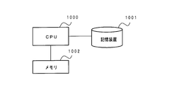
- each component in the information processing circuit design device 500 is realized by a computer having a processor such as a CPU (Central Processing Unit) or a memory, for example, it can be realized by a computer having a CPU shown in FIG. ..
- the computer realizes each function in the information processing circuit design device 500 shown in FIG. 4 by the CPU 1000 executing a process (information processing circuit design process) according to a program stored in the storage device 1001. That is, the computer realizes the functions of the parameter table optimization unit 501, the parameter table generation unit 502, the parallel degree determination unit 503, and the arithmetic unit generation unit 504 in the information processing circuit design device 500 shown in FIG.
- the storage device 1001 is, for example, a non-transitory computer readable medium.
- a non-temporary computer-readable medium is one of various types of tangible storage medium. Specific examples of non-temporary computer-readable media include magnetic recording media (for example, hard disk drives), magneto-optical recording media (for example, magneto-optical disks), CD-ROMs (Compact Disc-Read Only Memory), and CD-Rs (CD-Rs). Compact Disc-Recordable), CD-R / W (Compact Disc-ReWritable), semiconductor memory (for example, mask ROM, PROM (Programmable ROM), EPROM (Erasable PROM), flash ROM).
- magnetic recording media for example, hard disk drives
- magneto-optical recording media for example, magneto-optical disks
- CD-ROMs Compact Disc-Read Only Memory
- CD-Rs Compact Disc-Recordable
- CD-R / W Compact Disc-ReWritable
- semiconductor memory for example, mask ROM, PRO
- the program may also be stored on various types of temporary computer-readable media (transitory computer readable medium).
- the program is supplied to the temporary computer-readable medium, for example, via a wired or wireless communication path, that is, via an electrical signal, an optical signal, or an electromagnetic wave.
- the memory 1002 is realized by, for example, a RAM (Random Access Memory), and is a storage means for temporarily storing data when the CPU 1000 executes a process.
- a mode in which a program held by the storage device 1001 or a temporary computer-readable medium is transferred to the memory 1002 and the CPU 1000 executes processing based on the program in the memory 1002 can be assumed.
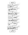
- the parameter table optimization unit 501 inputs the parameter set (plurality of parameter values) learned in the learning phase, and the parallel degree determination unit 503 inputs data indicating a predetermined network structure (step S11). ..
- VGG-16 As a type of deep learning algorithm which is one of the concepts of the network structure in the present embodiment, for example, AlexNet, GoogLeNet, ResNet (Residual Network), SENEt (Squeeze-and-Excitation Networks), MobileNet, VGG-16, etc. There is VGG-19. Further, as the number of layers, which is one of the concepts of the network structure, for example, the number of layers according to the type of the deep learning algorithm can be considered. In addition, filter size and the like can be included as a concept of network structure.
- inputting data indicating the network structure is expressed as inputting the network structure.
- the parallel degree determination unit 503 determines the parallel degree for each layer (step S12). As an example, the parallel degree determination unit 503 determines the parallel degree N by the equation (1). For example, when the number of layers specified by the type of input deep learning algorithm is 19, the parallel degree determination unit 503 determines the parallel degree of each of the 19 layers.
- N C L / DL ... (1)
- C L denotes a number of clocks required for all pixels of one screen in the parallel degree determination target layer (target layer) to process a single multiplier-adder.
- D L denotes the number of clocks required for one display of the processor in the target layer (the number of clocks allowed).
- one screen processes one vertical and horizontal pixel in one clock in a layer (referred to as a layer in the first block) having a vertical size of 224 and a horizontal size of 224 (50,176 pixels). It is assumed that the entire screen is executed at 50,176 clocks.
- a layer in which one screen has a vertical size of 14 and a horizontal size of 14 (referred to as a layer in the fifth block)
- processing of one vertical and horizontal pixel is performed with 256 clocks. If executed, the processing for one screen can be completed in 50, 176 clocks, which is the same as the first clock.
- the degree of parallelism of the layer of the fifth block is 9,216.
- the arithmetic unit of each layer (specifically, a plurality of basic circuits 300 included in the arithmetic unit) can be kept in operation at all times. In the configuration shown in FIG. 13, when no ingenuity is applied to the arithmetic units 701 to 706, the operating rate of the arithmetic unit 706 is lower than the operating rate of the arithmetic unit 701.
- Non-Patent Document 1 Taking the configuration described in Non-Patent Document 1 as an example, since each layer is fully-parallel, the operating rate of the arithmetic unit is lower in the layer close to the output layer. However, in the present embodiment, it is possible to maintain a high operating rate of the arithmetic units of all layers.
- the parameter table optimization unit 501 generates the parameter table 302 for each layer according to the determined degree of parallelism (step S13). Further, the parameter table optimization unit 501 optimizes the generated parameter table 302 (step S14).
- FIG. 7 is a flowchart showing an example of the process of optimizing the parameter table 302 (parameter table optimization process).
- the parameter table optimizing unit 501 measures the recognition accuracy of the CNN (inference device) (S141).
- the parameter table optimization unit 501 executes a simulation using an inferior using a number of basic circuits 300 and a circuit configuration of the parameter table according to the determined degree of parallelism. Simulation is inference using appropriate input data. Then, the recognition accuracy is obtained by comparing the simulation result with the correct answer.
- the parameter table optimizing unit 501 confirms whether or not the recognition accuracy is equal to or higher than the first reference value (step S142).
- the first reference value is a predetermined threshold value.
- the parameter table optimizing unit 501 estimates the circuit area of the parameter table 302. Then, it is confirmed whether or not the circuit area of the parameter table 302 is equal to or less than the second reference value (step S144).
- the second reference value is a predetermined threshold value.
- the parameter table optimization unit 501 can estimate the circuit area of the parameter table 302 based on, for example, the number of logic circuits in the combinational circuits constituting the parameter table 302.
- the parameter table optimization unit 501 ends the parameter table optimization process.
- step S143 If the recognition accuracy is less than the first reference value, or if the circuit area of the parameter table 302 exceeds the second reference value, the parameter table optimization unit 501 changes the parameter value (step S143). .. Then, the process proceeds to step S141.
- step S143 when the recognition accuracy is less than the first reference value, the parameter table optimizing unit 501 changes the parameter value in the direction in which the recognition accuracy is expected to improve.
- the parameter table optimizing unit 501 may change the parameter value by cut and try.
- step S143 when the circuit area of the parameter table 302 exceeds the second reference value, the parameter table optimization unit 501 changes the parameter value so that the circuit area of the parameter table 302 becomes smaller.
- a method of changing the parameter value for reducing the circuit area of the parameter table 302 for example, there are the following methods.
- the parameter value whose absolute value is smaller than the predetermined threshold value is changed to 0.
- the parameter value (positive number) larger than the predetermined threshold value is replaced with the maximum parameter value in the parameter table 302.
- a representative value is set for each predetermined area in the parameter table 302, and all the parameter values in the area are replaced with the representative values.
- typical values are even-numbered values, odd-numbered values, mode values, and the like.
- the parameter table optimization unit 501 may use one of the above-mentioned plurality of methods, or may use two or more of the above-mentioned plurality of methods in combination.
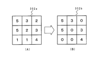
- FIG. 8 is an explanatory diagram showing an example of how to change the parameter value.
- FIG. 8 illustrates a parameter table having a size of 3 ⁇ 3.
- FIG. 8A shows the parameter table 302a before the parameter value is changed.
- FIG. 8B shows the parameter table 302b after the parameter values have been changed.
- the parameter value smaller than the predetermined threshold value “3” is changed to “0”.
- the purpose common to each of the above methods is to make the same value appear frequently in the parameter table 302, that is, to increase the parameter value of the same value or to make the same pattern continuous.
- the meaning that the same pattern is continuous means that, for example, the patterns of the parameter values "1", "2", and "3" (an example of the same pattern) appear continuously.
- the parameter table 302 when the parameter table 302 is realized by a combinational circuit, the smaller the number of types of parameter values, the smaller the circuit scale of the combinational circuit. Further, even when the same pattern is continuous, it is expected that the circuit scale of the combinational circuit becomes smaller.
- the recognition accuracy of the inference device is equal to or higher than a desired level (specifically, equal to or higher than the first reference value), and the circuit area is equal to or lower than a desired size (specifically). Specifically, when the value is equal to or less than the second reference value), the parameter table optimization process is terminated.
- the arithmetic unit generation unit 504 generates and outputs the circuit configuration of the arithmetic unit for each layer (steps S15 and S17). That is, the arithmetic unit generation unit 504 outputs the circuit configuration of the arithmetic unit according to the parallelism degree for each layer determined by the parallelism degree determination unit 503.
- the arithmetic unit generation unit 504 since the basic circuits 300 of each layer are predetermined, the arithmetic unit generation unit 504 has a number of basic circuits 300 (specifically, the number of basic circuits 300 according to the degree of parallelism determined by the parallel degree determination unit 503). , A product-sum circuit 301) specialized for layers is generated.
- the parameter table generation unit 502 generates and outputs the circuit configuration of the parameter table 302 (steps S16 and S17). That is, the parameter table generation unit 502 generates and outputs a circuit configuration for outputting the parameter values optimized by the parameter table optimization unit 501.
- the circuit configuration for outputting the parameter value is, for example, the configuration of a combinational circuit that realizes the truth table as illustrated in FIG. 3 (B).
- the parallel degree determination unit 503 determines an appropriate degree of parallelism, so that the effect of reducing the circuit scale can be obtained. it can.
- the parameter table 302 is realized by the combinational circuit, it is configured to read the parameter value shown in FIG. 12 from the memory.
- the processing speed is improved compared to the information processing circuit.
- the degree of parallelism of each layer in the inference device is determined according to the calculation speed desired for that layer, the operation of the calculation unit of all layers is compared with the case where each layer is fully-parallel. The rate can be kept high.
- the circuit scale is smaller than that in the case where each layer is fully-parallel. As a result, the power consumption of the inferior is reduced.
- the circuit scale of the inference device can be made smaller.
- the information processing circuit has been described using a CNN inference device as an example, but the present embodiment may be applied to another network having a layer for performing operations using input data and parameter values. it can. Further, in the present embodiment, the image data is used as the input data, but the present embodiment can also be utilized in a network in which the input data is other than the image data.
- the power consumption of the data center is large, it is desirable to execute it with low power consumption when the deep learning algorithm is executed in the data center.
- the power consumption is reduced, so that the information processing circuit of the present embodiment can be effectively used in the data center.
- the information processing circuit of this embodiment can be effectively used even on the edge side.
- FIG. 9 is a block diagram showing a main part of the information processing circuit.
- the information processing circuit 10 is a product-sum circuit 11 (in the embodiment, realized by the product-sum circuit 301) that executes a layer operation in deep learning and performs a product-sum operation using input data and parameter values.
- a parameter value output circuit 12 that outputs a parameter value (in the embodiment, it is realized by the parameter table 302), and the parameter value output circuit 12 is composed of a combinational circuit.
- FIG. 10 is a block diagram showing a main part of the information processing circuit design device.
- the information processing circuit design device 20 is a device that generates an information processing circuit that executes layer operations in deep learning, and is an input means 21 for inputting a plurality of learned parameter values and data that can identify a network structure. (In the embodiment, it is realized as a part of the parameter table optimization unit 501 and a part of the parallelism determination unit 503.)
- An arithmetic unit generation means 22 (in the embodiment, realized by the arithmetic unit generation unit 504) that creates a product-sum circuit specialized for layers in the structure, and a parameter value that creates a combination circuit that outputs a plurality of parameter values. It includes an output circuit creating means 23 (in the embodiment, it is realized by the parameter table generation unit 502).
- Appendix 1 An information processing circuit that executes layer operations in deep learning.
- a product-sum circuit that performs a product-sum operation using input data and parameter values, It is equipped with a parameter value output circuit that outputs the parameter value.
- the parameter value output circuit is an information processing circuit characterized in that it is composed of a combinational circuit.
- Appendix 2 Equipped with a number of basic circuits according to the number of parallel processes
- Each of the plurality of basic circuits is an information processing circuit according to Appendix 1, which includes the product-sum circuit and the parameter value output circuit.
- the basic circuit has a circuit configuration specialized for layers.
- the parameter value output circuit is an information processing circuit according to Appendix 2 that outputs the parameter value which is a fixed value.
- a method of designing an information processing circuit that generates an information processing circuit that executes layer operations in deep learning. Enter multiple trained parameter values and data that can identify the network structure, A product-sum circuit that performs a product-sum operation using input data and parameter values and is specialized for layers in the network structure is created.
- a method for designing an information processing circuit which comprises creating a combinational circuit that outputs a plurality of parameter values.
- Appendix 5 The information processing circuit design method of Appendix 4 for creating the product-sum circuit for each layer and the combinational circuit for each layer when deep learning is realized in a plurality of layers.
- Appendix 6 Determine the degree of parallelism based on the calculation speed required for the layer. The method for designing an information processing circuit according to Appendix 4 or 5, wherein a product-sum circuit of a number corresponding to the degree of parallelism is created.
- Appendix 7 A method for designing an information processing circuit according to any one of Appendix 4 to Appendix 6 in which one or more of the plurality of input parameter values are changed so that the parameter values having the same value increase.
- Appendix 8 An information processing circuit according to any one of Appendix 4 to Appendix 7 that changes one or more of the input plurality of parameter values so that a pattern consisting of the plurality of parameter values appears consecutively. Design method.
- the information processing circuit design program is The process of inputting multiple learned parameter values and data that can identify the network structure, A circuit that performs a product-sum operation using input data and parameter values, and a process that creates a product-sum circuit specialized for layers in the network structure. It is characterized in that the processor executes the process of creating a combinational circuit that outputs a plurality of parameter values.
- the information processing circuit design program is The recording medium of Appendix 10 which causes a processor to execute a process of creating the product-sum circuit for each layer and the combinational circuit for each layer when deep learning is realized by a plurality of layers.
- the information processing circuit design program is The process of determining the degree of parallelism based on the calculation speed required for the layer, The recording medium of Appendix 10 or Appendix 11 that causes the processor to execute the process of creating a product-sum circuit of a number corresponding to the degree of parallelism.
- the information processing circuit design program is A recording medium according to any one of Appendix 10 to Appendix 12, which causes a processor to execute a process of changing one or more of the input plurality of parameter values so that the parameter values having the same value increase.
- An information processing circuit design device that generates an information processing circuit that executes layer operations in deep learning.
- An input means for inputting multiple learned parameter values and data that can identify the network structure,
- An information processing circuit design device including a parameter value output circuit creating means for creating a combinational circuit that outputs a plurality of parameter values.
- a parallel degree determining means for determining the parallel degree based on the calculation speed required for the layer is provided.
- the arithmetic unit generating means is an information processing circuit design device according to Appendix 14 or Appendix 15 that creates a product-sum circuit of a number corresponding to the degree of parallelism.
- Appendix 17 Information of any one of Appendix 14 to Appendix 16 provided with a parameter optimization means for changing one or more of the plurality of input parameter values so that the parameter values having the same value increase. Processing circuit design equipment.
- Appendix 18 A program for generating an information processing circuit that executes layer operations in deep learning. On the computer The process of inputting multiple learned parameter values and data that can identify the network structure, A circuit that performs a product-sum operation using input data and parameter values, and a process that creates a product-sum circuit specialized for layers in the network structure. An information processing circuit design program for executing the process of creating a combinational circuit that outputs a plurality of parameter values.
- Appendix 19 To the computer The information processing circuit design program of Appendix 18 for creating the product-sum circuit for each layer and the combinational circuit for each layer when deep learning is realized in a plurality of layers.
- Appendix 20 To the computer The process of determining the degree of parallelism based on the calculation speed required for the layer, The information processing circuit design program of Appendix 18 or Appendix 19 for executing the process of creating a product-sum circuit of a number corresponding to the degree of parallelism.
- Appendix 21 To the computer A design program for an information processing circuit according to any one of Appendix 18 to Appendix 20, which executes a process of changing one or more of the input plurality of parameter values so that the parameter values having the same value increase.
- Information processing circuit 11 Information processing circuit 11
- Product sum circuit 12 Parameter value output circuit 20
- Information processing circuit design device 21 Input means 22
- Arithmetic generator generation means 23
- Parameter value output circuit creation means 100
- Arithmetic Instrument 211,212,213,214,215,216 Parameter 300 Basic circuit 301 Sum of products circuit 302 Parameter table 303 Register 400
- Control unit 500 Information processing circuit design device 501
- Parameter table optimization unit 502 Parameter table generation unit 503
- Parallelism determination unit 504 Arithmetic generator 1000
- CPU 1001 storage device 1002 memory
Landscapes
- Engineering & Computer Science (AREA)
- Physics & Mathematics (AREA)
- Theoretical Computer Science (AREA)
- General Physics & Mathematics (AREA)
- General Engineering & Computer Science (AREA)
- Computing Systems (AREA)
- Mathematical Physics (AREA)
- Biomedical Technology (AREA)
- Biophysics (AREA)
- Life Sciences & Earth Sciences (AREA)
- Health & Medical Sciences (AREA)
- Data Mining & Analysis (AREA)
- Mathematical Analysis (AREA)
- Computational Mathematics (AREA)
- Mathematical Optimization (AREA)
- Pure & Applied Mathematics (AREA)
- Software Systems (AREA)
- Molecular Biology (AREA)
- General Health & Medical Sciences (AREA)
- Evolutionary Computation (AREA)
- Computational Linguistics (AREA)
- Artificial Intelligence (AREA)
- Neurology (AREA)
- Algebra (AREA)
- Databases & Information Systems (AREA)
- Design And Manufacture Of Integrated Circuits (AREA)
- Complex Calculations (AREA)
Priority Applications (4)
| Application Number | Priority Date | Filing Date | Title |
|---|---|---|---|
| JP2021554008A JP7310910B2 (ja) | 2019-10-31 | 2019-10-31 | 情報処理回路および情報処理回路の設計方法 |
| US17/771,143 US20220413806A1 (en) | 2019-10-31 | 2019-10-31 | Information processing circuit and method of designing information processing circuit |
| PCT/JP2019/042927 WO2021084717A1 (ja) | 2019-10-31 | 2019-10-31 | 情報処理回路および情報処理回路の設計方法 |
| TW109128738A TWI830940B (zh) | 2019-10-31 | 2020-08-24 | 資訊處理電路以及資訊處理電路的設計方法 |
Applications Claiming Priority (1)
| Application Number | Priority Date | Filing Date | Title |
|---|---|---|---|
| PCT/JP2019/042927 WO2021084717A1 (ja) | 2019-10-31 | 2019-10-31 | 情報処理回路および情報処理回路の設計方法 |
Publications (1)
| Publication Number | Publication Date |
|---|---|
| WO2021084717A1 true WO2021084717A1 (ja) | 2021-05-06 |
Family
ID=75714945
Family Applications (1)
| Application Number | Title | Priority Date | Filing Date |
|---|---|---|---|
| PCT/JP2019/042927 Ceased WO2021084717A1 (ja) | 2019-10-31 | 2019-10-31 | 情報処理回路および情報処理回路の設計方法 |
Country Status (4)
| Country | Link |
|---|---|
| US (1) | US20220413806A1 (https=) |
| JP (1) | JP7310910B2 (https=) |
| TW (1) | TWI830940B (https=) |
| WO (1) | WO2021084717A1 (https=) |
Families Citing this family (1)
| Publication number | Priority date | Publication date | Assignee | Title |
|---|---|---|---|---|
| JP7456501B2 (ja) * | 2020-05-26 | 2024-03-27 | 日本電気株式会社 | 情報処理回路および情報処理回路の設計方法 |
Citations (3)
| Publication number | Priority date | Publication date | Assignee | Title |
|---|---|---|---|---|
| JP2004086374A (ja) * | 2002-08-23 | 2004-03-18 | Ricoh Co Ltd | 半導体装置 |
| JP2018124754A (ja) * | 2017-01-31 | 2018-08-09 | 日本電信電話株式会社 | 多層ニューラルネットの大局構造抽出装置、方法、及びプログラム |
| JP2018132830A (ja) * | 2017-02-13 | 2018-08-23 | LeapMind株式会社 | ニューラルネットワーク構築方法、ニューラルネットワーク装置及びニューラルネットワーク装置更新方法 |
Family Cites Families (5)
| Publication number | Priority date | Publication date | Assignee | Title |
|---|---|---|---|---|
| US10552732B2 (en) * | 2016-08-22 | 2020-02-04 | Kneron Inc. | Multi-layer neural network |
| US11586907B2 (en) * | 2018-02-27 | 2023-02-21 | Stmicroelectronics S.R.L. | Arithmetic unit for deep learning acceleration |
| JP2019168851A (ja) * | 2018-03-22 | 2019-10-03 | 東芝メモリ株式会社 | 演算装置及び演算方法 |
| CN108764467B (zh) * | 2018-04-04 | 2021-08-17 | 北京大学深圳研究生院 | 用于卷积神经网络卷积运算和全连接运算电路 |
| WO2020095140A1 (ja) * | 2018-11-08 | 2020-05-14 | 株式会社半導体エネルギー研究所 | 半導体装置、及び電子機器 |
-
2019
- 2019-10-31 WO PCT/JP2019/042927 patent/WO2021084717A1/ja not_active Ceased
- 2019-10-31 JP JP2021554008A patent/JP7310910B2/ja active Active
- 2019-10-31 US US17/771,143 patent/US20220413806A1/en active Pending
-
2020
- 2020-08-24 TW TW109128738A patent/TWI830940B/zh active
Patent Citations (3)
| Publication number | Priority date | Publication date | Assignee | Title |
|---|---|---|---|---|
| JP2004086374A (ja) * | 2002-08-23 | 2004-03-18 | Ricoh Co Ltd | 半導体装置 |
| JP2018124754A (ja) * | 2017-01-31 | 2018-08-09 | 日本電信電話株式会社 | 多層ニューラルネットの大局構造抽出装置、方法、及びプログラム |
| JP2018132830A (ja) * | 2017-02-13 | 2018-08-23 | LeapMind株式会社 | ニューラルネットワーク構築方法、ニューラルネットワーク装置及びニューラルネットワーク装置更新方法 |
Non-Patent Citations (1)
| Title |
|---|
| WHATMOUGH PAUL N. ET AL.: "FixyNN: Efficient Hardware for Mobile Computer Vision via Transfer Learning", ARXIV:1902.11128V1, 27 February 2019 (2019-02-27), pages 1 - 13, XP081034882, Retrieved from the Internet <URL:https://arxiv.org/pdf/1902.11128.pdf> * |
Also Published As
| Publication number | Publication date |
|---|---|
| TWI830940B (zh) | 2024-02-01 |
| JPWO2021084717A1 (https=) | 2021-05-06 |
| US20220413806A1 (en) | 2022-12-29 |
| TW202119256A (zh) | 2021-05-16 |
| JP7310910B2 (ja) | 2023-07-19 |
Similar Documents
| Publication | Publication Date | Title |
|---|---|---|
| US11137981B2 (en) | Operation processing device, information processing device, and information processing method | |
| JP6977864B2 (ja) | 推論装置、畳み込み演算実行方法及びプログラム | |
| KR102853349B1 (ko) | 인공 신경 네트워크를 자동으로 조정하는 방법 및 장치 | |
| US10656962B2 (en) | Accelerate deep neural network in an FPGA | |
| US20190347072A1 (en) | Block floating point computations using shared exponents | |
| US12136039B1 (en) | Optimizing global sparsity for neural network | |
| EP3528181A1 (en) | Processing method of neural network and apparatus using the processing method | |
| Fan et al. | Reconfigurable acceleration of 3D-CNNs for human action recognition with block floating-point representation | |
| CN107861916A (zh) | 一种用于针对神经网络执行非线性运算的方法和装置 | |
| CN110265002A (zh) | 语音识别方法、装置、计算机设备及计算机可读存储介质 | |
| CN113869517A (zh) | 一种基于深度学习模型的推理方法 | |
| US12299555B2 (en) | Training network with discrete weight values | |
| US20240143986A1 (en) | Methods and systems for executing a neural network on a neural network accelerator | |
| US11551087B2 (en) | Information processor, information processing method, and storage medium | |
| US20230185533A1 (en) | Configurable nonlinear activation function circuits | |
| JP7310910B2 (ja) | 情報処理回路および情報処理回路の設計方法 | |
| JP2020067897A (ja) | 演算処理装置、学習プログラム及び学習方法 | |
| CN116187155A (zh) | 生成最佳输入数据的计算设备和方法 | |
| JP7456501B2 (ja) | 情報処理回路および情報処理回路の設計方法 | |
| GB2620172A (en) | Identifying one or more quantisation parameters for quantising values to be processed by a neural network | |
| US12124939B1 (en) | Generation of machine-trained network instructions | |
| Mihiraamsh et al. | Analysis of Multiply-Accumulate (MAC) Unit Using Convolution Neural Networks (CNN) | |
| JP2020190901A (ja) | 演算処理装置、演算処理装置の制御プログラム及び演算処理装置の制御方法 | |
| KR102953802B1 (ko) | 활성화 함수 희소성을 이용하여 최적화되는 가속기와 상기 가속기의 연산 방법 | |
| US20260004039A1 (en) | Integrated circuit floorplan generation using generative artificial intelligence models |
Legal Events
| Date | Code | Title | Description |
|---|---|---|---|
| 121 | Ep: the epo has been informed by wipo that ep was designated in this application |
Ref document number: 19950979 Country of ref document: EP Kind code of ref document: A1 |
|
| ENP | Entry into the national phase |
Ref document number: 2021554008 Country of ref document: JP Kind code of ref document: A |
|
| NENP | Non-entry into the national phase |
Ref country code: DE |
|
| 122 | Ep: pct application non-entry in european phase |
Ref document number: 19950979 Country of ref document: EP Kind code of ref document: A1 |