WO2021084717A1 - Iinformation processing circuit and method of designing information processing circuit - Google Patents
Iinformation processing circuit and method of designing information processing circuit Download PDFInfo
- Publication number
- WO2021084717A1 WO2021084717A1 PCT/JP2019/042927 JP2019042927W WO2021084717A1 WO 2021084717 A1 WO2021084717 A1 WO 2021084717A1 JP 2019042927 W JP2019042927 W JP 2019042927W WO 2021084717 A1 WO2021084717 A1 WO 2021084717A1
- Authority
- WO
- WIPO (PCT)
- Prior art keywords
- circuit
- information processing
- processing circuit
- layer
- parameter
- Prior art date
Links
Images


Classifications
-
- G—PHYSICS
- G06—COMPUTING; CALCULATING OR COUNTING
- G06F—ELECTRIC DIGITAL DATA PROCESSING
- G06F7/00—Methods or arrangements for processing data by operating upon the order or content of the data handled
- G06F7/38—Methods or arrangements for performing computations using exclusively denominational number representation, e.g. using binary, ternary, decimal representation
- G06F7/48—Methods or arrangements for performing computations using exclusively denominational number representation, e.g. using binary, ternary, decimal representation using non-contact-making devices, e.g. tube, solid state device; using unspecified devices
- G06F7/544—Methods or arrangements for performing computations using exclusively denominational number representation, e.g. using binary, ternary, decimal representation using non-contact-making devices, e.g. tube, solid state device; using unspecified devices for evaluating functions by calculation
- G06F7/5443—Sum of products
-
- G—PHYSICS
- G06—COMPUTING; CALCULATING OR COUNTING
- G06F—ELECTRIC DIGITAL DATA PROCESSING
- G06F17/00—Digital computing or data processing equipment or methods, specially adapted for specific functions
- G06F17/10—Complex mathematical operations
- G06F17/16—Matrix or vector computation, e.g. matrix-matrix or matrix-vector multiplication, matrix factorization
-
- G—PHYSICS
- G06—COMPUTING; CALCULATING OR COUNTING
- G06N—COMPUTING ARRANGEMENTS BASED ON SPECIFIC COMPUTATIONAL MODELS
- G06N3/00—Computing arrangements based on biological models
- G06N3/02—Neural networks
- G06N3/04—Architecture, e.g. interconnection topology
- G06N3/0464—Convolutional networks [CNN, ConvNet]
-
- G—PHYSICS
- G06—COMPUTING; CALCULATING OR COUNTING
- G06N—COMPUTING ARRANGEMENTS BASED ON SPECIFIC COMPUTATIONAL MODELS
- G06N3/00—Computing arrangements based on biological models
- G06N3/02—Neural networks
- G06N3/06—Physical realisation, i.e. hardware implementation of neural networks, neurons or parts of neurons
- G06N3/063—Physical realisation, i.e. hardware implementation of neural networks, neurons or parts of neurons using electronic means
-
- G—PHYSICS
- G06—COMPUTING; CALCULATING OR COUNTING
- G06N—COMPUTING ARRANGEMENTS BASED ON SPECIFIC COMPUTATIONAL MODELS
- G06N3/00—Computing arrangements based on biological models
- G06N3/02—Neural networks
- G06N3/04—Architecture, e.g. interconnection topology
- G06N3/045—Combinations of networks
Definitions
- the present invention relates to an information processing circuit that executes an inference phase of deep learning, and a method for designing such an information processing circuit.
- Deep learning is an algorithm that uses a multi-layer neural network (hereinafter referred to as a network).
- a learning phase in which each network (layer) is optimized to create a model (learning model) and an inference phase in which inference is performed based on the learning model are executed.
- the model is sometimes called an inference model.
- the model may be expressed as an inference device below.
- an inference device realized by a GPU Graphics Processing Unit
- CPU Central Processing Unit
- an accelerator dedicated to deep learning has been put into practical use.
- FIG. 11 is an explanatory diagram showing the structure of VGG (Visual Geometry Group) -16, which is an example of a convolutional neural network (CNN).
- VGG-16 includes 13 convolutional layers and 3 fully connected layers. The features extracted in the convolution layer, or in the convolution layer and the pooling layer, are classified as fully connected layers.
- the convolution layer is a 3 ⁇ 3 convolution. Therefore, for example, the first convolution operation in FIG. 11 includes a product-sum operation of 3 (vertical size) ⁇ 3 (horizontal size) ⁇ 3 (input channel) ⁇ 64 (output channel) per pixel. Further, for example, the convolution layer of the fifth block in FIG. 11 includes a product-sum operation of 3 (vertical size) ⁇ 3 (horizontal size) ⁇ 512 (input channel) ⁇ 512 (output channel) per pixel.
- “P” indicates a pooling layer. In the CNN shown in FIG. 11, the pooling layer is the Max Pooling layer.
- F indicates a fully connected layer.
- O indicates an output layer.
- the convolution layer and the fully connected layer include a normalized linear unit (ReLU).
- the multiplication formula attached to each layer represents the vertical size ⁇ horizontal size ⁇ number of channels of the data corresponding to one input image. Also, the volume of the rectangular parallelepiped representing the layer corresponds to the amount of activation in the layer.
- CNN is configured so that operations of a plurality of layers constituting CNN are executed by a common arithmetic unit (see, for example, paragraph 0033 of Patent Document 1). ).
- FIG. 12 is an explanatory diagram schematically showing a CNN arithmetic unit configured so that operations of a plurality of layers are executed by a common arithmetic unit.
- the part that executes the calculation in the inference unit is composed of the arithmetic unit 700 and the memory (for example, DRAM (Dynamic Random Access Memory) 900).
- the arithmetic unit 700 shown in FIG. 12 has a large number of adders and a large number of multiplications. A device is formed.
- “+” indicates an adder.
- “*” Indicates a multiplier.
- three adders and six multipliers are exemplified. However, a number of adders and multipliers are formed in which each operation of all layers in the CNN can be performed.
- the arithmetic unit 700 When the operation of each layer of the inferior is executed, the arithmetic unit 700 reads the parameters for the layer to be executed from the DRAM 900. Then, the arithmetic unit 700 executes the product-sum operation in one layer with the parameter as a coefficient.
- the CNN is configured so that the operations of each of all the layers constituting the CNN (particularly, the convolutional layer) are executed by the arithmetic unit corresponding to each layer (for example, Non-Patent Document 1). reference).
- Non-Patent Document 1 describes that the CNN is divided into two stages, and an arithmetic unit corresponding to each layer is provided in the previous stage.
- FIG. 13 is an explanatory diagram schematically showing a CNN provided with an arithmetic unit corresponding to each layer.
- FIG. 13 illustrates the six layers 801,802,803,804,805,806 in CNN.
- Arithmetic units (circuits) 701, 702, 703, 704, 705, 706 corresponding to each of the layers 801, 802, 803, 804, 805, 806 are provided.
- Non-Patent Document 1 describes that the parameter is set to a fixed value.
- the CNN function is executed without changing the circuit configuration of the arithmetic units 701 to 706 even if the parameters are changed.
- the data transfer rate of the DRAM 900 is lower than the calculation speed of the arithmetic unit 700. That is, the memory band of the DRAM 900 is narrow. Therefore, the data transfer between the arithmetic circuit 700 and the memory becomes a bottleneck. As a result, the calculation speed of CNN is limited.
- the circuit scale of the adder and the multiplier as a whole of the CNN becomes small.
- the circuit scale is increased by such a circuit configuration. Since the circuit is configured to process the operations corresponding to each input channel and each output channel in parallel for each layer, the circuit scale is increased by such a circuit configuration. Further, since the circuit is configured so that completely parallel processing is possible for each layer, it is desirable that the processing time of the input data corresponding to one image is the same for each layer.
- the vertical size and horizontal size of the input data corresponding to one image may become smaller as the layer is closer to the output layer.
- the pooling layer reduces the vertical and horizontal sizes of the input data corresponding to one image. If each layer processes data corresponding to one input image in the same time, the amount of calculation in the previous layer becomes small unless the number of channels in the previous layer is extremely increased. In other words, the earlier the layer, the smaller the circuit scale for executing the operations of that layer.
- the arithmetic unit 700 since the arithmetic unit 700 is configured to be able to execute the arithmetic of all the input channels and the output channels in parallel, the layer having a small vertical size and horizontal size of the input data Is that the processing of the input data corresponding to one image is completed early, and a waiting time is generated until the input data corresponding to the next image is supplied. In other words, the utilization rate of the arithmetic unit 700 is low.
- the configuration of the CNN described in Non-Patent Document 1 is that the CNN is divided into two stages, and an arithmetic unit corresponding to each layer is provided in the previous stage. Then, the stage in the latter stage is configured so that the parameters are transferred to the DRAM and a programmable accelerator is used as the arithmetic unit. That is, it is described in Non-Patent Document 1 that the CNN is configured to respond to a certain degree of parameter change and network configuration change, and the parameter and network configuration are fixed as the CNN as a whole, that is, as the inferencer as a whole. It has not been.
- the present invention provides an information processing circuit and a method for designing an information processing circuit that, when the inference device is realized by hardware, is released from the limitation of the memory bandwidth and the utilization rate of the arithmetic unit of each layer in the inference device is improved.
- the purpose is to provide.
- the information processing circuit includes a product-sum circuit that executes layer operations in deep learning and performs product-sum operations using input data and parameter values, and a parameter value output circuit that outputs parameter values.
- the parameter value output circuit is composed of a combinational circuit.
- the information processing circuit design method is a design method for generating an information processing circuit that executes layer operations in deep learning, and inputs a plurality of learned parameter values and data capable of identifying a network structure. Then, a product-sum circuit that performs a product-sum operation using input data and parameter values and is specialized for layers in the network structure is created, and a combination circuit that outputs a plurality of parameter values is created.
- the information processing circuit design program is a program for generating an information processing circuit that executes layer operations in deep learning, and allows a computer to specify a plurality of learned parameter values and a network structure.
- the process of creating a combinational circuit is executed.
- the information processing circuit design device is a device that generates an information processing circuit that executes layer operations in deep learning, and is an input for inputting a plurality of learned parameter values and data that can identify a network structure.
- a means an arithmetic unit generating means for creating a sum-of-product circuit that is a circuit that performs a product-sum operation using input data and parameter values and is specialized for layers in a network structure, and a combination circuit that outputs a plurality of parameter values.
- the present invention it is possible to obtain an information processing circuit that is free from the restrictions of the memory bandwidth and that improves the utilization rate of the arithmetic unit of each layer in the inference device.
- a CNN inference device will be taken as an example.
- an image image data
- the information processing circuit is a CNN inference device provided with an arithmetic unit corresponding to each layer of the CNN. Then, in the information processing circuit, the parameters are fixed, and the network configuration (type of deep learning algorithm, what type of layer is arranged in what order, size of input data and size of output data of each layer, etc. ) Is fixed to realize a CNN inferior. That is, the information processing circuit is a circuit having a circuit configuration specialized for each layer of the CNN (for example, each of the convolution layer and the fully connected layer). Specializing means that it is a dedicated circuit that exclusively executes the operations of the relevant layer.
- the fixed parameters mean that the processing of the learning phase is completed, the appropriate parameters are determined, and the determined parameters are used.
- the parameters determined in the learning phase may be changed.
- changing a parameter may be expressed as optimizing the parameter.
- the degree of parallelism is determined in consideration of the data input speed, the processing speed, and the like.
- the multiplier of the parameter (weight) and the input data in the inference device is composed of a combination logic circuit (combination circuit). Alternatively, it may be composed of a pipeline arithmetic unit. Alternatively, it may be composed of a sequential circuit.
- FIG. 1 is an explanatory diagram schematically showing the information processing circuit of the present embodiment.
- FIG. 1 illustrates the arithmetic units 201, 202, 203, 204, 205, and 206 in the information processing circuit 100 that realizes CNN. That is, FIG. 1 illustrates 6 layers of CNN.
- Each arithmetic unit 201, 202, 203, 204, 205, 206 executes a product-sum operation for the parameters 211,212,213,214,215,216 used in the layer and the input data.
- the arithmetic units 201 to 206 are realized by a plurality of combinational circuits. Parameters 211 to 216 are also realized by the combinational circuit.
- the combinational circuit is a negative logical product circuit (NAND circuit), a negative logical sum circuit (NOR circuit), a negative circuit (inverting circuit: NOT circuit), and a combination thereof.
- NAND circuit negative logical product circuit
- NOR circuit negative logical sum circuit
- NOT circuit negative circuit
- one circuit element may be expressed as a combinational circuit, but a circuit including a plurality of circuit elements (NAND circuit, NOR circuit, NOT circuit, etc.) may be expressed as a combinational circuit.
- parallel operations are executed in each of the arithmetic units 201 to 206, and a circuit that executes one operation in the parallel operations is used as a basic circuit.
- the basic circuit is predetermined according to the type of layer.
- FIG. 2 is an explanatory diagram showing a configuration example of a basic circuit.
- the arithmetic units (circuits) 201, 202, 203, 204, 205, and 206 of the six layers are exemplified.
- a basic circuit 300 for the number of parallel processes is provided in each layer.
- the basic circuit 300 included in the arithmetic unit 203 is illustrated in FIG. 2, the arithmetic units 201, 202, 204, 205, and 206 of other layers also have the same circuit configuration.
- the basic circuit 300 includes a product-sum circuit 301 that multiplies the input data and the parameter values from the parameter table (weight table) 302 and adds the multiplied values.
- the input data may be one value. Further, the input data may be a set of a plurality of values.
- FIG. 2 shows a parameter table 302 for storing parameter values, the parameter values are not actually stored in the storage unit (storage circuit), and the parameter table 302 is combined. It is realized by the circuit.
- the parameter table 302 since the parameters are fixed, the parameter values, which are fixed values, are output from the parameter table 302.
- the parameter table 302 may output one value. Further, the parameter table 302 may output a plurality of sets of values.
- the product-sum circuit 301 may multiply one input value and one parameter value. Further, the product-sum calculator 301 may multiply the set of input values and the set of parameter values. You may calculate the aggregate sum of the set of the multiplication result of the set of the input value and the set of the parameter value. In general, a plurality of parameters or a plurality of sets of parameters are used for one layer, and the control unit 400 controls which parameter is output.
- the basic circuit 300 may include a register 303 that temporarily stores the product-sum operation value.
- the product-sum circuit 301 may include an adder that adds a plurality of multiplication values temporarily stored in the register 303.
- the output of another basic circuit 300 may be connected to the input of the basic circuit 300.
- FIG. 3 is an explanatory diagram for explaining a circuit configuration example of the parameter table 302.
- FIG. 3A shows an example of the truth table 311.
- the truth table 311 can be realized by the combinational circuit.
- Each of A, B, and C is an input of a combinational circuit.
- Z1 and Z2 are outputs of the combinational circuit.
- the truth table 311 of the full adder is shown as an example, but A, B, and C can be regarded as addresses, and Z1 and Z2 can be regarded as output data. That is, Z1 and Z2 can be regarded as output data for the designated addresses A, B, and C.
- By associating the output data with the parameter value a desired parameter value can be obtained according to some input (designated address).
- the parameter value is simplified to be determined by the inputs B and C in the truth table 311. All you have to do is use the truth table 312.
- the circuit scale of the combinational circuit becomes smaller as the number of different types of inputs for determining the parameters decreases.
- a known technique such as the Quine-McCluskey method is used to simplify the truth table.
- the arithmetic unit 203 shown in FIG. 2 includes a control unit 400.
- the control unit 400 controls the data of the designated address corresponding to the output data at a desired timing. Is supplied to the parameter table 302.
- the parameter table 302 outputs the output data corresponding to the designated address, that is, the parameter value to the product-sum circuit 301.
- the desired timing is when the product-sum circuit 301 executes the multiplication process using the parameter values to be output from the parameter table 302.
- FIG. 4 is a block diagram showing an example of an information processing circuit design device for designing the circuit configuration of the parameter table of each layer of CNN and the circuit configuration of the arithmetic unit.
- the information processing circuit design device 500 includes a parameter table optimization unit 501, a parameter table generation unit 502, a parallel degree determination unit 503, and an arithmetic unit generation unit 504.
- the parallel degree determination unit 503 inputs a network structure (specifically, data indicating the network structure).
- the arithmetic unit generation unit 504 outputs the circuit configuration of the arithmetic unit for each layer.
- the parameter table optimization unit 501 inputs the parameter set (weight in each layer) learned in the learning phase and the parallel degree determined by the parallel degree determination unit 503.
- the parameter table generation unit 502 outputs the circuit configuration of the parameter table.
- the parallel degree determination unit 503 determines the parallel degree for each layer.
- the parameter table optimization unit 501 optimizes the parameter table based on the input parameters for each layer and the degree of parallelism for each layer determined by the parallel degree determination unit 503.
- the number of parameter tables is determined by the degree of parallelism, and the parameter table optimization unit 501 optimizes each parameter in the plurality of parameter tables 302.
- optimization means reducing the circuit area of the combinational circuit corresponding to the parameter table.
- the degree of parallelism is determined to be "128”
- the number of basic circuits 300 is 128.
- Each basic circuit 300 is a product of 1152 pieces.
- the process for the operation (147,456 / 128) is executed.
- the basic circuit 300 is provided with only 128 parameter tables having the parameter values of 1152.
- the parameter table 302 is stored. It is not realized by a circuit, but by a combination circuit.
- the parameter table optimization unit 501 optimizes the parameter values of the parameter table 302 by using a predetermined method.
- the parameter table generation unit 502 outputs the circuit configuration for realizing the parameter table 302 having the optimized parameter values as the circuit configuration of the parameter table.
- the arithmetic unit generation unit 504 inputs the degree of parallelism for each layer determined by the degree of parallelism determination unit 503.
- the arithmetic unit generation unit 504 generates a circuit configuration in which the number of basic circuits 300 indicated by the degree of parallelism are arranged for each layer. Then, the arithmetic unit generation unit 504 outputs the generated circuit configuration for each layer as the configuration of the arithmetic unit circuit.
- Each component in the information processing circuit design device 500 shown in FIG. 4 can be configured by one hardware or one software. Further, each component can be configured by a plurality of hardware or a plurality of software. It is also possible to configure a part of each component with hardware and another part with software.
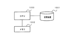
- each component in the information processing circuit design device 500 is realized by a computer having a processor such as a CPU (Central Processing Unit) or a memory, for example, it can be realized by a computer having a CPU shown in FIG. ..
- the computer realizes each function in the information processing circuit design device 500 shown in FIG. 4 by the CPU 1000 executing a process (information processing circuit design process) according to a program stored in the storage device 1001. That is, the computer realizes the functions of the parameter table optimization unit 501, the parameter table generation unit 502, the parallel degree determination unit 503, and the arithmetic unit generation unit 504 in the information processing circuit design device 500 shown in FIG.
- the storage device 1001 is, for example, a non-transitory computer readable medium.
- a non-temporary computer-readable medium is one of various types of tangible storage medium. Specific examples of non-temporary computer-readable media include magnetic recording media (for example, hard disk drives), magneto-optical recording media (for example, magneto-optical disks), CD-ROMs (Compact Disc-Read Only Memory), and CD-Rs (CD-Rs). Compact Disc-Recordable), CD-R / W (Compact Disc-ReWritable), semiconductor memory (for example, mask ROM, PROM (Programmable ROM), EPROM (Erasable PROM), flash ROM).
- magnetic recording media for example, hard disk drives
- magneto-optical recording media for example, magneto-optical disks
- CD-ROMs Compact Disc-Read Only Memory
- CD-Rs Compact Disc-Recordable
- CD-R / W Compact Disc-ReWritable
- semiconductor memory for example, mask ROM, PRO
- the program may also be stored on various types of temporary computer-readable media (transitory computer readable medium).
- the program is supplied to the temporary computer-readable medium, for example, via a wired or wireless communication path, that is, via an electrical signal, an optical signal, or an electromagnetic wave.
- the memory 1002 is realized by, for example, a RAM (Random Access Memory), and is a storage means for temporarily storing data when the CPU 1000 executes a process.
- a mode in which a program held by the storage device 1001 or a temporary computer-readable medium is transferred to the memory 1002 and the CPU 1000 executes processing based on the program in the memory 1002 can be assumed.
- the parameter table optimization unit 501 inputs the parameter set (plurality of parameter values) learned in the learning phase, and the parallel degree determination unit 503 inputs data indicating a predetermined network structure (step S11). ..
- VGG-16 As a type of deep learning algorithm which is one of the concepts of the network structure in the present embodiment, for example, AlexNet, GoogLeNet, ResNet (Residual Network), SENEt (Squeeze-and-Excitation Networks), MobileNet, VGG-16, etc. There is VGG-19. Further, as the number of layers, which is one of the concepts of the network structure, for example, the number of layers according to the type of the deep learning algorithm can be considered. In addition, filter size and the like can be included as a concept of network structure.
- inputting data indicating the network structure is expressed as inputting the network structure.
- the parallel degree determination unit 503 determines the parallel degree for each layer (step S12). As an example, the parallel degree determination unit 503 determines the parallel degree N by the equation (1). For example, when the number of layers specified by the type of input deep learning algorithm is 19, the parallel degree determination unit 503 determines the parallel degree of each of the 19 layers.
- N C L / DL ... (1)
- C L denotes a number of clocks required for all pixels of one screen in the parallel degree determination target layer (target layer) to process a single multiplier-adder.
- D L denotes the number of clocks required for one display of the processor in the target layer (the number of clocks allowed).
- one screen processes one vertical and horizontal pixel in one clock in a layer (referred to as a layer in the first block) having a vertical size of 224 and a horizontal size of 224 (50,176 pixels). It is assumed that the entire screen is executed at 50,176 clocks.
- a layer in which one screen has a vertical size of 14 and a horizontal size of 14 (referred to as a layer in the fifth block)
- processing of one vertical and horizontal pixel is performed with 256 clocks. If executed, the processing for one screen can be completed in 50, 176 clocks, which is the same as the first clock.
- the degree of parallelism of the layer of the fifth block is 9,216.
- the arithmetic unit of each layer (specifically, a plurality of basic circuits 300 included in the arithmetic unit) can be kept in operation at all times. In the configuration shown in FIG. 13, when no ingenuity is applied to the arithmetic units 701 to 706, the operating rate of the arithmetic unit 706 is lower than the operating rate of the arithmetic unit 701.
- Non-Patent Document 1 Taking the configuration described in Non-Patent Document 1 as an example, since each layer is fully-parallel, the operating rate of the arithmetic unit is lower in the layer close to the output layer. However, in the present embodiment, it is possible to maintain a high operating rate of the arithmetic units of all layers.
- the parameter table optimization unit 501 generates the parameter table 302 for each layer according to the determined degree of parallelism (step S13). Further, the parameter table optimization unit 501 optimizes the generated parameter table 302 (step S14).
- FIG. 7 is a flowchart showing an example of the process of optimizing the parameter table 302 (parameter table optimization process).
- the parameter table optimizing unit 501 measures the recognition accuracy of the CNN (inference device) (S141).
- the parameter table optimization unit 501 executes a simulation using an inferior using a number of basic circuits 300 and a circuit configuration of the parameter table according to the determined degree of parallelism. Simulation is inference using appropriate input data. Then, the recognition accuracy is obtained by comparing the simulation result with the correct answer.
- the parameter table optimizing unit 501 confirms whether or not the recognition accuracy is equal to or higher than the first reference value (step S142).
- the first reference value is a predetermined threshold value.
- the parameter table optimizing unit 501 estimates the circuit area of the parameter table 302. Then, it is confirmed whether or not the circuit area of the parameter table 302 is equal to or less than the second reference value (step S144).
- the second reference value is a predetermined threshold value.
- the parameter table optimization unit 501 can estimate the circuit area of the parameter table 302 based on, for example, the number of logic circuits in the combinational circuits constituting the parameter table 302.
- the parameter table optimization unit 501 ends the parameter table optimization process.
- step S143 If the recognition accuracy is less than the first reference value, or if the circuit area of the parameter table 302 exceeds the second reference value, the parameter table optimization unit 501 changes the parameter value (step S143). .. Then, the process proceeds to step S141.
- step S143 when the recognition accuracy is less than the first reference value, the parameter table optimizing unit 501 changes the parameter value in the direction in which the recognition accuracy is expected to improve.
- the parameter table optimizing unit 501 may change the parameter value by cut and try.
- step S143 when the circuit area of the parameter table 302 exceeds the second reference value, the parameter table optimization unit 501 changes the parameter value so that the circuit area of the parameter table 302 becomes smaller.
- a method of changing the parameter value for reducing the circuit area of the parameter table 302 for example, there are the following methods.
- the parameter value whose absolute value is smaller than the predetermined threshold value is changed to 0.
- the parameter value (positive number) larger than the predetermined threshold value is replaced with the maximum parameter value in the parameter table 302.
- a representative value is set for each predetermined area in the parameter table 302, and all the parameter values in the area are replaced with the representative values.
- typical values are even-numbered values, odd-numbered values, mode values, and the like.
- the parameter table optimization unit 501 may use one of the above-mentioned plurality of methods, or may use two or more of the above-mentioned plurality of methods in combination.
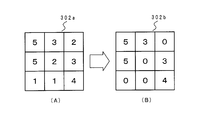
- FIG. 8 is an explanatory diagram showing an example of how to change the parameter value.
- FIG. 8 illustrates a parameter table having a size of 3 ⁇ 3.
- FIG. 8A shows the parameter table 302a before the parameter value is changed.
- FIG. 8B shows the parameter table 302b after the parameter values have been changed.
- the parameter value smaller than the predetermined threshold value “3” is changed to “0”.
- the purpose common to each of the above methods is to make the same value appear frequently in the parameter table 302, that is, to increase the parameter value of the same value or to make the same pattern continuous.
- the meaning that the same pattern is continuous means that, for example, the patterns of the parameter values "1", "2", and "3" (an example of the same pattern) appear continuously.
- the parameter table 302 when the parameter table 302 is realized by a combinational circuit, the smaller the number of types of parameter values, the smaller the circuit scale of the combinational circuit. Further, even when the same pattern is continuous, it is expected that the circuit scale of the combinational circuit becomes smaller.
- the recognition accuracy of the inference device is equal to or higher than a desired level (specifically, equal to or higher than the first reference value), and the circuit area is equal to or lower than a desired size (specifically). Specifically, when the value is equal to or less than the second reference value), the parameter table optimization process is terminated.
- the arithmetic unit generation unit 504 generates and outputs the circuit configuration of the arithmetic unit for each layer (steps S15 and S17). That is, the arithmetic unit generation unit 504 outputs the circuit configuration of the arithmetic unit according to the parallelism degree for each layer determined by the parallelism degree determination unit 503.
- the arithmetic unit generation unit 504 since the basic circuits 300 of each layer are predetermined, the arithmetic unit generation unit 504 has a number of basic circuits 300 (specifically, the number of basic circuits 300 according to the degree of parallelism determined by the parallel degree determination unit 503). , A product-sum circuit 301) specialized for layers is generated.
- the parameter table generation unit 502 generates and outputs the circuit configuration of the parameter table 302 (steps S16 and S17). That is, the parameter table generation unit 502 generates and outputs a circuit configuration for outputting the parameter values optimized by the parameter table optimization unit 501.
- the circuit configuration for outputting the parameter value is, for example, the configuration of a combinational circuit that realizes the truth table as illustrated in FIG. 3 (B).
- the parallel degree determination unit 503 determines an appropriate degree of parallelism, so that the effect of reducing the circuit scale can be obtained. it can.
- the parameter table 302 is realized by the combinational circuit, it is configured to read the parameter value shown in FIG. 12 from the memory.
- the processing speed is improved compared to the information processing circuit.
- the degree of parallelism of each layer in the inference device is determined according to the calculation speed desired for that layer, the operation of the calculation unit of all layers is compared with the case where each layer is fully-parallel. The rate can be kept high.
- the circuit scale is smaller than that in the case where each layer is fully-parallel. As a result, the power consumption of the inferior is reduced.
- the circuit scale of the inference device can be made smaller.
- the information processing circuit has been described using a CNN inference device as an example, but the present embodiment may be applied to another network having a layer for performing operations using input data and parameter values. it can. Further, in the present embodiment, the image data is used as the input data, but the present embodiment can also be utilized in a network in which the input data is other than the image data.
- the power consumption of the data center is large, it is desirable to execute it with low power consumption when the deep learning algorithm is executed in the data center.
- the power consumption is reduced, so that the information processing circuit of the present embodiment can be effectively used in the data center.
- the information processing circuit of this embodiment can be effectively used even on the edge side.
- FIG. 9 is a block diagram showing a main part of the information processing circuit.
- the information processing circuit 10 is a product-sum circuit 11 (in the embodiment, realized by the product-sum circuit 301) that executes a layer operation in deep learning and performs a product-sum operation using input data and parameter values.
- a parameter value output circuit 12 that outputs a parameter value (in the embodiment, it is realized by the parameter table 302), and the parameter value output circuit 12 is composed of a combinational circuit.
- FIG. 10 is a block diagram showing a main part of the information processing circuit design device.
- the information processing circuit design device 20 is a device that generates an information processing circuit that executes layer operations in deep learning, and is an input means 21 for inputting a plurality of learned parameter values and data that can identify a network structure. (In the embodiment, it is realized as a part of the parameter table optimization unit 501 and a part of the parallelism determination unit 503.)
- An arithmetic unit generation means 22 (in the embodiment, realized by the arithmetic unit generation unit 504) that creates a product-sum circuit specialized for layers in the structure, and a parameter value that creates a combination circuit that outputs a plurality of parameter values. It includes an output circuit creating means 23 (in the embodiment, it is realized by the parameter table generation unit 502).
- Appendix 1 An information processing circuit that executes layer operations in deep learning.
- a product-sum circuit that performs a product-sum operation using input data and parameter values, It is equipped with a parameter value output circuit that outputs the parameter value.
- the parameter value output circuit is an information processing circuit characterized in that it is composed of a combinational circuit.
- Appendix 2 Equipped with a number of basic circuits according to the number of parallel processes
- Each of the plurality of basic circuits is an information processing circuit according to Appendix 1, which includes the product-sum circuit and the parameter value output circuit.
- the basic circuit has a circuit configuration specialized for layers.
- the parameter value output circuit is an information processing circuit according to Appendix 2 that outputs the parameter value which is a fixed value.
- a method of designing an information processing circuit that generates an information processing circuit that executes layer operations in deep learning. Enter multiple trained parameter values and data that can identify the network structure, A product-sum circuit that performs a product-sum operation using input data and parameter values and is specialized for layers in the network structure is created.
- a method for designing an information processing circuit which comprises creating a combinational circuit that outputs a plurality of parameter values.
- Appendix 5 The information processing circuit design method of Appendix 4 for creating the product-sum circuit for each layer and the combinational circuit for each layer when deep learning is realized in a plurality of layers.
- Appendix 6 Determine the degree of parallelism based on the calculation speed required for the layer. The method for designing an information processing circuit according to Appendix 4 or 5, wherein a product-sum circuit of a number corresponding to the degree of parallelism is created.
- Appendix 7 A method for designing an information processing circuit according to any one of Appendix 4 to Appendix 6 in which one or more of the plurality of input parameter values are changed so that the parameter values having the same value increase.
- Appendix 8 An information processing circuit according to any one of Appendix 4 to Appendix 7 that changes one or more of the input plurality of parameter values so that a pattern consisting of the plurality of parameter values appears consecutively. Design method.
- the information processing circuit design program is The process of inputting multiple learned parameter values and data that can identify the network structure, A circuit that performs a product-sum operation using input data and parameter values, and a process that creates a product-sum circuit specialized for layers in the network structure. It is characterized in that the processor executes the process of creating a combinational circuit that outputs a plurality of parameter values.
- the information processing circuit design program is The recording medium of Appendix 10 which causes a processor to execute a process of creating the product-sum circuit for each layer and the combinational circuit for each layer when deep learning is realized by a plurality of layers.
- the information processing circuit design program is The process of determining the degree of parallelism based on the calculation speed required for the layer, The recording medium of Appendix 10 or Appendix 11 that causes the processor to execute the process of creating a product-sum circuit of a number corresponding to the degree of parallelism.
- the information processing circuit design program is A recording medium according to any one of Appendix 10 to Appendix 12, which causes a processor to execute a process of changing one or more of the input plurality of parameter values so that the parameter values having the same value increase.
- An information processing circuit design device that generates an information processing circuit that executes layer operations in deep learning.
- An input means for inputting multiple learned parameter values and data that can identify the network structure,
- An information processing circuit design device including a parameter value output circuit creating means for creating a combinational circuit that outputs a plurality of parameter values.
- a parallel degree determining means for determining the parallel degree based on the calculation speed required for the layer is provided.
- the arithmetic unit generating means is an information processing circuit design device according to Appendix 14 or Appendix 15 that creates a product-sum circuit of a number corresponding to the degree of parallelism.
- Appendix 17 Information of any one of Appendix 14 to Appendix 16 provided with a parameter optimization means for changing one or more of the plurality of input parameter values so that the parameter values having the same value increase. Processing circuit design equipment.
- Appendix 18 A program for generating an information processing circuit that executes layer operations in deep learning. On the computer The process of inputting multiple learned parameter values and data that can identify the network structure, A circuit that performs a product-sum operation using input data and parameter values, and a process that creates a product-sum circuit specialized for layers in the network structure. An information processing circuit design program for executing the process of creating a combinational circuit that outputs a plurality of parameter values.
- Appendix 19 To the computer The information processing circuit design program of Appendix 18 for creating the product-sum circuit for each layer and the combinational circuit for each layer when deep learning is realized in a plurality of layers.
- Appendix 20 To the computer The process of determining the degree of parallelism based on the calculation speed required for the layer, The information processing circuit design program of Appendix 18 or Appendix 19 for executing the process of creating a product-sum circuit of a number corresponding to the degree of parallelism.
- Appendix 21 To the computer A design program for an information processing circuit according to any one of Appendix 18 to Appendix 20, which executes a process of changing one or more of the input plurality of parameter values so that the parameter values having the same value increase.
- Information processing circuit 11 Information processing circuit 11
- Product sum circuit 12 Parameter value output circuit 20
- Information processing circuit design device 21 Input means 22
- Arithmetic generator generation means 23
- Parameter value output circuit creation means 100
- Arithmetic Instrument 211,212,213,214,215,216 Parameter 300 Basic circuit 301 Sum of products circuit 302 Parameter table 303 Register 400
- Control unit 500 Information processing circuit design device 501
- Parameter table optimization unit 502 Parameter table generation unit 503
- Parallelism determination unit 504 Arithmetic generator 1000
- CPU 1001 storage device 1002 memory
Landscapes
- Engineering & Computer Science (AREA)
- Physics & Mathematics (AREA)
- Theoretical Computer Science (AREA)
- General Physics & Mathematics (AREA)
- General Engineering & Computer Science (AREA)
- Computing Systems (AREA)
- Mathematical Physics (AREA)
- Biomedical Technology (AREA)
- Biophysics (AREA)
- Life Sciences & Earth Sciences (AREA)
- Health & Medical Sciences (AREA)
- Data Mining & Analysis (AREA)
- Mathematical Analysis (AREA)
- Computational Mathematics (AREA)
- Mathematical Optimization (AREA)
- Pure & Applied Mathematics (AREA)
- Software Systems (AREA)
- Molecular Biology (AREA)
- General Health & Medical Sciences (AREA)
- Evolutionary Computation (AREA)
- Computational Linguistics (AREA)
- Artificial Intelligence (AREA)
- Neurology (AREA)
- Algebra (AREA)
- Databases & Information Systems (AREA)
- Design And Manufacture Of Integrated Circuits (AREA)
Abstract
This information processing circuit 10 comprises: a product sum circuit 11 which executes a layered operation in deep learning, and performs a product sum operation by using input data and a parameter value; and a parameter value output circuit 12 which outputs the parameter value, wherein the parameter value output circuit 12 is configured from a combinational circuit.
Description
本発明は、深層学習の推論フェーズを実行する情報処理回路、およびそのような情報処理回路の設計方法に関する。
The present invention relates to an information processing circuit that executes an inference phase of deep learning, and a method for designing such an information processing circuit.
深層学習は、多層のニューラルネットワーク(以下、ネットワークという。)を使用するアルゴリズムである。深層学習では、各々のネットワーク(層)を最適化してモデル(学習モデル)を作成する学習フェーズと、学習モデルに基づいて推論が行われる推論フェーズとが実行される。なお、モデルは、推論モデルといわれることもある。また、以下、モデルを推論器と表現することがある。
Deep learning is an algorithm that uses a multi-layer neural network (hereinafter referred to as a network). In deep learning, a learning phase in which each network (layer) is optimized to create a model (learning model) and an inference phase in which inference is performed based on the learning model are executed. The model is sometimes called an inference model. In addition, the model may be expressed as an inference device below.
学習フェーズおよび推論フェーズにおいて、パラメタとしての重みを調整するための演算が実行されたり、入力データと重みとを対象とする演算が行われるが、それらの演算の計算量は多い。その結果、各々のフェーズの処理時間が長くなる。
In the learning phase and the inference phase, operations for adjusting weights as parameters are executed, and operations for input data and weights are performed, but the amount of calculation of these operations is large. As a result, the processing time of each phase becomes long.
深層学習を高速化するために、CPU(Central Processing Unit )によって実現される推論器ではなく、GPU(Graphics Processing Unit)によって実現される推論器がよく用いられる。さらに、深層学習専用のアクセラレータが実用化されている。
In order to speed up deep learning, an inference device realized by a GPU (Graphics Processing Unit) is often used instead of an inference device realized by a CPU (Central Processing Unit). Furthermore, an accelerator dedicated to deep learning has been put into practical use.
図11は、畳み込みニューラルネットワーク(CNN:Convolutional Neural Network)の一例であるVGG(Visual Geometry Group )-16の構造を示す説明図である。VGG-16は、13層の畳み込み層および3層の全結合層を含む。畳み込み層で、または畳み込み層とプーリング層とで抽出された特徴は、全結合層で分類される。
FIG. 11 is an explanatory diagram showing the structure of VGG (Visual Geometry Group) -16, which is an example of a convolutional neural network (CNN). VGG-16 includes 13 convolutional layers and 3 fully connected layers. The features extracted in the convolution layer, or in the convolution layer and the pooling layer, are classified as fully connected layers.
図11において、「I」は入力層を示す。「C」は畳み込み層を示す。図11において、畳み込み層は3×3の畳み込みである。よって、たとえば、図11の最初の畳み込み演算には1画素あたり3(縦サイズ)×3(横サイズ)×3(入力チャネル)×64(出力チャネル)個の積和演算を含む。また例えば図11の5ブロック目の畳み込み層には、1画素あたり3(縦サイズ)×3(横サイズ)×512(入力チャネル)×512(出力チャネル)個の積和演算を含む。「P」はプーリング層を示す。図11に示すCNNでは、プーリング層は、Max Pooling 層である。「F」は全結合層を示す。「O」は出力層を示す。出力層では、softmax関数が使用される。なお、畳み込み層および全結合層は、正規化線形ユニット(Rectified Linear Unit :ReLU)を含む。各層に付されている乗算式は、一枚の入力画像に対応するデータの縦サイズ×横サイズ×チャネル数を表す。また、層を表す直方体の体積は、層におけるアクティベーションの量に対応する。
In FIG. 11, "I" indicates an input layer. "C" indicates a convolution layer. In FIG. 11, the convolution layer is a 3 × 3 convolution. Therefore, for example, the first convolution operation in FIG. 11 includes a product-sum operation of 3 (vertical size) × 3 (horizontal size) × 3 (input channel) × 64 (output channel) per pixel. Further, for example, the convolution layer of the fifth block in FIG. 11 includes a product-sum operation of 3 (vertical size) × 3 (horizontal size) × 512 (input channel) × 512 (output channel) per pixel. "P" indicates a pooling layer. In the CNN shown in FIG. 11, the pooling layer is the Max Pooling layer. "F" indicates a fully connected layer. "O" indicates an output layer. In the output layer, the softmax function is used. The convolution layer and the fully connected layer include a normalized linear unit (ReLU). The multiplication formula attached to each layer represents the vertical size × horizontal size × number of channels of the data corresponding to one input image. Also, the volume of the rectangular parallelepiped representing the layer corresponds to the amount of activation in the layer.
アクセラレータで推論器を実現する場合、主として2つの方法が考えられる。
When realizing an inference device with an accelerator, there are mainly two possible methods.
CNNを例にすると、第1の方法では、CNNは、CNNを構成する複数の層の演算が共通の演算器で実行されるように構成される(例えば、特許文献1の段落0033等参照。)。
Taking CNN as an example, in the first method, CNN is configured so that operations of a plurality of layers constituting CNN are executed by a common arithmetic unit (see, for example, paragraph 0033 of Patent Document 1). ).
図12は、複数の層の演算が共通の演算器で実行されるように構成されたCNNの演算器を模式的に示す説明図である。推論器における演算を実行する部分は、演算器700とメモリ(例えば、DRAM(Dynamic Random Access Memory)900とで構成される。図12に示す演算器700には、多数の加算器と多数の乗算器とが形成される。図12において、「+」は加算器を示す。「*」は乗算器を示す。なお、図12には、3つの加算器と6個の乗算器とが例示されているが、CNNにおける全ての層の各々の演算が実行可能な数の加算器と乗算器とが形成されている。
FIG. 12 is an explanatory diagram schematically showing a CNN arithmetic unit configured so that operations of a plurality of layers are executed by a common arithmetic unit. The part that executes the calculation in the inference unit is composed of the arithmetic unit 700 and the memory (for example, DRAM (Dynamic Random Access Memory) 900). The arithmetic unit 700 shown in FIG. 12 has a large number of adders and a large number of multiplications. A device is formed. In FIG. 12, “+” indicates an adder. “*” Indicates a multiplier. In FIG. 12, three adders and six multipliers are exemplified. However, a number of adders and multipliers are formed in which each operation of all layers in the CNN can be performed.
推論器の各層の演算が実行される場合、演算器700は、演算実行対象の一層についてのパラメタをDRAM900から読み出す。そして、演算器700は、一層における積和演算を、パラメタを係数として実行する。
When the operation of each layer of the inferior is executed, the arithmetic unit 700 reads the parameters for the layer to be executed from the DRAM 900. Then, the arithmetic unit 700 executes the product-sum operation in one layer with the parameter as a coefficient.
第2の方法では、CNNは、CNNを構成する全ての層の各々(特に、畳み込み層)の演算を、各層に対応する演算器で実行されるように構成される(例えば、非特許文献1参照)。なお、非特許文献1には、CNNが2つのステージに分割され、前段のステージにおいて、各々の層に対応する演算器が設けられることが記載されている。
In the second method, the CNN is configured so that the operations of each of all the layers constituting the CNN (particularly, the convolutional layer) are executed by the arithmetic unit corresponding to each layer (for example, Non-Patent Document 1). reference). It should be noted that Non-Patent Document 1 describes that the CNN is divided into two stages, and an arithmetic unit corresponding to each layer is provided in the previous stage.
図13は、各々の層に対応する演算器が設けられたCNNを模式的に示す説明図である。図13には、CNNにおける6つの層801,802,803,804,805,806が例示されている。層801,802,803,804,805,806のそれぞれに対応する演算器(回路)701,702,703,704,705,706が設けられている。
FIG. 13 is an explanatory diagram schematically showing a CNN provided with an arithmetic unit corresponding to each layer. FIG. 13 illustrates the six layers 801,802,803,804,805,806 in CNN. Arithmetic units (circuits) 701, 702, 703, 704, 705, 706 corresponding to each of the layers 801, 802, 803, 804, 805, 806 are provided.
演算器701~706は、対応する層801~806の演算を実行するので、パラメタが不変であれば、固定的に回路構成される。そして、非特許文献1には、パラメタを固定値にすることが記載されている。
Since the arithmetic units 701 to 706 execute the operations of the corresponding layers 801 to 806, if the parameters are unchanged, the circuit is fixedly configured. Then, Non-Patent Document 1 describes that the parameter is set to a fixed value.
上記の第1の方法では、DRAM900が備えられているので、パラメタが変更されても、演算器701~706の回路構成を変更することなく、CNNの機能が実行される。しかし、DRAM900のデータ転送速度は、演算器700の演算速度と比較すると低速である。すなわち、DRAM900のメモリ帯域は狭い。したがって、演算回路700とメモリの間のデータ転送がボトルネックになる。その結果、CNNの演算速度が制限される。
In the first method described above, since the DRAM 900 is provided, the CNN function is executed without changing the circuit configuration of the arithmetic units 701 to 706 even if the parameters are changed. However, the data transfer rate of the DRAM 900 is lower than the calculation speed of the arithmetic unit 700. That is, the memory band of the DRAM 900 is narrow. Therefore, the data transfer between the arithmetic circuit 700 and the memory becomes a bottleneck. As a result, the calculation speed of CNN is limited.
上記の第2の方法では、各層のそれぞれに対応する演算器701~706が設けられるので、CNN全体としての回路規模が大きくなる。
In the second method described above, since the arithmetic units 701 to 706 corresponding to each layer are provided, the circuit scale of the CNN as a whole becomes large.
非特許文献1に記載された方法では、パラメタおよびネットワーク構成を固定することによって、CNN全体としての加算器と乗算器の回路規模が小さくなる。ただし、非特許文献1に記載された方法では、各層に関して、完全に並列処理が可能であるように(fully-parallel)回路構成されるので、そのような回路構成によって、回路規模は大きくなる。なお、各層に関して各入力チャネル、各出力チャネルに対応する演算を並列処理するように回路構成されるので、そのような回路構成によって、回路規模は大きくなる。また、各層に関して、完全に並列処理が可能であるように回路構成されるので、一枚の画像に対応する入力データの処理時間は各層において同じ時間であることが望ましい。
In the method described in Non-Patent Document 1, by fixing the parameters and the network configuration, the circuit scale of the adder and the multiplier as a whole of the CNN becomes small. However, in the method described in Non-Patent Document 1, since the circuit is configured so as to be able to perform completely parallel processing for each layer (fully-parallel), the circuit scale is increased by such a circuit configuration. Since the circuit is configured to process the operations corresponding to each input channel and each output channel in parallel for each layer, the circuit scale is increased by such a circuit configuration. Further, since the circuit is configured so that completely parallel processing is possible for each layer, it is desirable that the processing time of the input data corresponding to one image is the same for each layer.
CNNでは、先の層(出力層に近い層)であるほど、一枚の画像に対応する入力データの縦サイズや横サイズが小さくなる場合がある。例えばプーリング層によって一枚の画像に対応する入力データの縦サイズと横サイズが縮小される。各層が同じ時間で一枚の入力画像に対応するデータを処理するとした場合、先の層のチャネル数を極端に多くしない限り、先の層での計算量は小さくなる。換言すれば、本来、先の層であるほど、その層の演算を実行する回路規模は小さくてよい。しかし、非特許文献1に記載された方法では、演算器700は、すべての入力チャネルと出力チャネルの演算を並列に実行可能に構成されるので、入力データの縦サイズと横サイズが少ない層については、一枚の画像に対応する入力データの処理が早く終わり、次の画像に対応する入力データが供給されるまで待ち時間が発生する。換言すれば演算器700の利用率は低くなる。
In CNN, the vertical size and horizontal size of the input data corresponding to one image may become smaller as the layer is closer to the output layer. For example, the pooling layer reduces the vertical and horizontal sizes of the input data corresponding to one image. If each layer processes data corresponding to one input image in the same time, the amount of calculation in the previous layer becomes small unless the number of channels in the previous layer is extremely increased. In other words, the earlier the layer, the smaller the circuit scale for executing the operations of that layer. However, in the method described in Non-Patent Document 1, since the arithmetic unit 700 is configured to be able to execute the arithmetic of all the input channels and the output channels in parallel, the layer having a small vertical size and horizontal size of the input data Is that the processing of the input data corresponding to one image is completed early, and a waiting time is generated until the input data corresponding to the next image is supplied. In other words, the utilization rate of the arithmetic unit 700 is low.
また、非特許文献1に記載されたCNNの構成は、CNNが2つのステージに分割され、前段のステージにおいて各々の層に対応する演算器が設けられるという構成である。そして、後段のステージは、DRAMにパラメタが転送され、演算器としてプログラマブルなアクセラレータを用いるように構成される。すなわち、CNNは、ある程度のパラメタの変更やネットワーク構成の変更に応えられるように構成され、CNN全体として、すなわち、推論器全体として、パラメタおよびネットワーク構成を固定することは、非特許文献1に記載されていない。
Further, the configuration of the CNN described in Non-Patent Document 1 is that the CNN is divided into two stages, and an arithmetic unit corresponding to each layer is provided in the previous stage. Then, the stage in the latter stage is configured so that the parameters are transferred to the DRAM and a programmable accelerator is used as the arithmetic unit. That is, it is described in Non-Patent Document 1 that the CNN is configured to respond to a certain degree of parameter change and network configuration change, and the parameter and network configuration are fixed as the CNN as a whole, that is, as the inferencer as a whole. It has not been.
本発明は、推論器がハードウエアで実現される場合に、メモリ帯域の制約から解放され、かつ、推論器における各層の演算器の利用率が向上する情報処理回路および情報処理回路の設計方法を提供することを目的とする。
The present invention provides an information processing circuit and a method for designing an information processing circuit that, when the inference device is realized by hardware, is released from the limitation of the memory bandwidth and the utilization rate of the arithmetic unit of each layer in the inference device is improved. The purpose is to provide.
本発明による情報処理回路は、深層学習における層の演算を実行し、入力データとパラメタ値とを用いて積和演算を行う積和回路と、パラメタ値を出力するパラメタ値出力回路とを含み、パラメタ値出力回路は、組み合わせ回路で構成されている。
The information processing circuit according to the present invention includes a product-sum circuit that executes layer operations in deep learning and performs product-sum operations using input data and parameter values, and a parameter value output circuit that outputs parameter values. The parameter value output circuit is composed of a combinational circuit.
本発明による情報処理回路の設計方法は、深層学習における層の演算を実行する情報処理回路を生成する設計方法であって、学習済みの複数のパラメタ値とネットワーク構造を特定可能なデータとを入力し、入力データとパラメタ値とを用いて積和演算を行う回路であってネットワーク構造における層に特化した積和回路を作成し、複数のパラメタ値を出力する組み合わせ回路を作成する。
The information processing circuit design method according to the present invention is a design method for generating an information processing circuit that executes layer operations in deep learning, and inputs a plurality of learned parameter values and data capable of identifying a network structure. Then, a product-sum circuit that performs a product-sum operation using input data and parameter values and is specialized for layers in the network structure is created, and a combination circuit that outputs a plurality of parameter values is created.
本発明による情報処理回路の設計プログラムは、深層学習における層の演算を実行する情報処理回路を生成するためのプログラムであって、コンピュータに、学習済みの複数のパラメタ値とネットワーク構造を特定可能なデータとを入力する処理と、入力データとパラメタ値とを用いて積和演算を行う回路であってネットワーク構造における層に特化した積和回路を作成する処理と、複数のパラメタ値を出力する組み合わせ回路を作成する処理とを実行させる。
The information processing circuit design program according to the present invention is a program for generating an information processing circuit that executes layer operations in deep learning, and allows a computer to specify a plurality of learned parameter values and a network structure. A process of inputting data, a process of creating a product-sum circuit that is a circuit that performs a product-sum operation using the input data and parameter values and is specialized for layers in the network structure, and a process of outputting a plurality of parameter values. The process of creating a combinational circuit is executed.
本発明による情報処理回路設計装置は、深層学習における層の演算を実行する情報処理回路を生成する装置であって、学習済みの複数のパラメタ値とネットワーク構造を特定可能なデータとを入力する入力手段と、入力データとパラメタ値とを用いて積和演算を行う回路であってネットワーク構造における層に特化した積和回路を作成する演算器生成手段と、複数のパラメタ値を出力する組み合わせ回路を作成するパラメタ値出力回路作成手段とを含む。
The information processing circuit design device according to the present invention is a device that generates an information processing circuit that executes layer operations in deep learning, and is an input for inputting a plurality of learned parameter values and data that can identify a network structure. A means, an arithmetic unit generating means for creating a sum-of-product circuit that is a circuit that performs a product-sum operation using input data and parameter values and is specialized for layers in a network structure, and a combination circuit that outputs a plurality of parameter values. Includes parameter value output circuit creation means to create.
本発明によれば、メモリ帯域の制約から解放され、かつ、推論器における各層の演算器の利用率が向上する情報処理回路を得ることができる。
According to the present invention, it is possible to obtain an information processing circuit that is free from the restrictions of the memory bandwidth and that improves the utilization rate of the arithmetic unit of each layer in the inference device.
以下、本発明の実施形態を図面を参照して説明する。以下、情報処理回路として、CNNの推論器を例にする。また、CNNに入力されるデータとして、画像(画像データ)を例にする。
Hereinafter, embodiments of the present invention will be described with reference to the drawings. Hereinafter, as an information processing circuit, a CNN inference device will be taken as an example. Further, as the data to be input to the CNN, an image (image data) will be taken as an example.
図13に例示された構成と同様に、情報処理回路は、CNNの各々の層に対応する演算器が設けられたCNNの推論器である。そして、情報処理回路は、パラメタが固定され、かつ、ネットワーク構成(深層学習アルゴリズムの種類、どのタイプの層を幾つどういった順で配置するのか、各層の入力データのサイズや出力データのサイズなど)が固定されたCNNの推論器を実現する。すなわち、情報処理回路は、CNNの各層(例えば、畳み込み層および全結合層のそれぞれ)に特化した回路構成の回路である。特化するというのは、専ら当該層の演算を実行する専用回路であるということである。
Similar to the configuration illustrated in FIG. 13, the information processing circuit is a CNN inference device provided with an arithmetic unit corresponding to each layer of the CNN. Then, in the information processing circuit, the parameters are fixed, and the network configuration (type of deep learning algorithm, what type of layer is arranged in what order, size of input data and size of output data of each layer, etc. ) Is fixed to realize a CNN inferior. That is, the information processing circuit is a circuit having a circuit configuration specialized for each layer of the CNN (for example, each of the convolution layer and the fully connected layer). Specializing means that it is a dedicated circuit that exclusively executes the operations of the relevant layer.
なお、パラメタが固定されているということは、学習フェーズの処理が終了して、適切なパラメタが決定され、決定されたパラメタが使用されることを意味する。ただし、本実施形態では、学習フェーズで決定されたパラメタが変更されることがある。以下、パラメタが変更されることを、パラメタが最適化されると表現することがある。
Note that the fixed parameters mean that the processing of the learning phase is completed, the appropriate parameters are determined, and the determined parameters are used. However, in the present embodiment, the parameters determined in the learning phase may be changed. Hereinafter, changing a parameter may be expressed as optimizing the parameter.
また、本発明による情報処理回路を用いる推論器では、並列度は、データ入力速度や処理速度などを勘案して決定される。推論器におけるパラメタ(重み)と入力データとの乗算器は、組み合わせ論理回路(組み合わせ回路)で構成される。もしくは、パイプライン演算器で構成されてもよい。もしくは、順序回路で構成されてもよい。
Further, in the inference device using the information processing circuit according to the present invention, the degree of parallelism is determined in consideration of the data input speed, the processing speed, and the like. The multiplier of the parameter (weight) and the input data in the inference device is composed of a combination logic circuit (combination circuit). Alternatively, it may be composed of a pipeline arithmetic unit. Alternatively, it may be composed of a sequential circuit.
図1は、本実施形態の情報処理回路を模式的に示す説明図である。図1には、CNNを実現する情報処理回路100における演算器201,202,203,204,205,206が例示されている。すなわち、図1には、CNNのうちの6層が例示されている。各演算器201,202,203,204,205,206は、層で使用されるパラメタ211,212,213,214,215,216と入力データとを対象として積和演算を実行する。演算器201~206は、複数の組み合わせ回路で実現される。パラメタ211~216も、組み合わせ回路で実現される。
FIG. 1 is an explanatory diagram schematically showing the information processing circuit of the present embodiment. FIG. 1 illustrates the arithmetic units 201, 202, 203, 204, 205, and 206 in the information processing circuit 100 that realizes CNN. That is, FIG. 1 illustrates 6 layers of CNN. Each arithmetic unit 201, 202, 203, 204, 205, 206 executes a product-sum operation for the parameters 211,212,213,214,215,216 used in the layer and the input data. The arithmetic units 201 to 206 are realized by a plurality of combinational circuits. Parameters 211 to 216 are also realized by the combinational circuit.
なお、組み合わせ回路は、否定論理積回路(NAND回路)、否定論理和回路(NOR回路)、否定回路(反転回路:NOT回路)、および、その組み合わせなどである。以下の説明において、1つの回路素子を組み合わせ回路と表現することもあるが、複数の回路素子(NAND回路、NOR回路、NOT回路など)を含む回路を組み合わせ回路と表現することもある。
The combinational circuit is a negative logical product circuit (NAND circuit), a negative logical sum circuit (NOR circuit), a negative circuit (inverting circuit: NOT circuit), and a combination thereof. In the following description, one circuit element may be expressed as a combinational circuit, but a circuit including a plurality of circuit elements (NAND circuit, NOR circuit, NOT circuit, etc.) may be expressed as a combinational circuit.
図1において、「+」は加算器を示す。「*」は乗算器を示す。なお、図1に例示された各層の演算器201~206のブロックに示されている加算器の数および乗算器の数は、表記のための単なる一例である。
In FIG. 1, "+" indicates an adder. "*" Indicates a multiplier. The number of adders and the number of multipliers shown in the blocks of the arithmetic units 201 to 206 of each layer illustrated in FIG. 1 are merely examples for notation.
本実施形態では、演算器201~206のそれぞれにおいて並列演算が実行されるが、並列演算における1つの演算を実行する回路を基本回路とする。基本回路は、層の種類に応じてあらかじめ決定されている。
In the present embodiment, parallel operations are executed in each of the arithmetic units 201 to 206, and a circuit that executes one operation in the parallel operations is used as a basic circuit. The basic circuit is predetermined according to the type of layer.
図2は、基本回路の構成例を示す説明図である。6つの層のそれぞれの演算器(回路)201,202,203,204,205,206が例示されている。各層において、並列処理数の基本回路300が設けられる。図2には、演算器203に含まれる基本回路300が例示されているが、他の層の演算器201,202,204,205,206も同様の回路構成を有する。
FIG. 2 is an explanatory diagram showing a configuration example of a basic circuit. The arithmetic units (circuits) 201, 202, 203, 204, 205, and 206 of the six layers are exemplified. In each layer, a basic circuit 300 for the number of parallel processes is provided. Although the basic circuit 300 included in the arithmetic unit 203 is illustrated in FIG. 2, the arithmetic units 201, 202, 204, 205, and 206 of other layers also have the same circuit configuration.
図2に示す例では、基本回路300は、入力データとパラメタテーブル(重みテーブル)302からのパラメタ値を乗算し、乗算値を加算する積和回路301を含む。入力データは1つの値であってもよい。また、入力データは複数の値の組であってもよい。なお、図2には、パラメタ値を格納するパラメタテーブル302が示されているが、実際には、パラメタ値は記憶部(記憶回路)に記憶されているのではなく、パラメタテーブル302は、組み合わせ回路で実現される。本実施形態では、パラメタが固定されているので、パラメタテーブル302から、固定的な値であるパラメタ値が出力される。パラメタテーブル302は、1つの値を出力してもよい。また、パラメタテーブル302は、複数の値の組を出力してもよい。積和回路301は、1つの入力値と1つのパラメタ値の乗算を行ってもよい。また、積和演算器301は、入力値の組とパラメタ値の組との乗算を行ってもよい。入力値の組とパラメタ値の組との乗算結果の組の集約和の計算を行ってもよい。なお、一般に、1つの層に関して複数のパラメタ、もしくは、複数の組のパラメタが使用される、どのパラメタを出力するかは制御部400が制御する。
In the example shown in FIG. 2, the basic circuit 300 includes a product-sum circuit 301 that multiplies the input data and the parameter values from the parameter table (weight table) 302 and adds the multiplied values. The input data may be one value. Further, the input data may be a set of a plurality of values. Although FIG. 2 shows a parameter table 302 for storing parameter values, the parameter values are not actually stored in the storage unit (storage circuit), and the parameter table 302 is combined. It is realized by the circuit. In the present embodiment, since the parameters are fixed, the parameter values, which are fixed values, are output from the parameter table 302. The parameter table 302 may output one value. Further, the parameter table 302 may output a plurality of sets of values. The product-sum circuit 301 may multiply one input value and one parameter value. Further, the product-sum calculator 301 may multiply the set of input values and the set of parameter values. You may calculate the aggregate sum of the set of the multiplication result of the set of the input value and the set of the parameter value. In general, a plurality of parameters or a plurality of sets of parameters are used for one layer, and the control unit 400 controls which parameter is output.
基本回路300は、積和演算値を一時格納するレジスタ303を含んでもよい。積和回路301は、レジスタ303に一時格納された複数の乗算値を加算する加算器を含んでもよい。基本回路300の入力には、別の基本回路300の出力が接続されていてもよい。
The basic circuit 300 may include a register 303 that temporarily stores the product-sum operation value. The product-sum circuit 301 may include an adder that adds a plurality of multiplication values temporarily stored in the register 303. The output of another basic circuit 300 may be connected to the input of the basic circuit 300.
図3は、パラメタテーブル302の回路構成例を説明するための説明図である。図3(A)には、真理値表311の一例が示されている。組み合わせ回路で、真理値表311を実現することができる。A,B,Cのそれぞれは、組み合わせ回路の入力である。Z1,Z2は、組み合わせ回路の出力である。図3(A)には、一例として、全加算器の真理値表311が示されているが、A,B,Cをアドレスと見なし、Z1,Z2を出力データと見なすことができる。すなわち、Z1,Z2を、指定アドレスA,B,Cに対する出力データと見なすことができる。出力データをパラメタ値に対応づけると、何らかの入力(指定アドレス)に応じて、所望のパラメタ値を得ることができる。
FIG. 3 is an explanatory diagram for explaining a circuit configuration example of the parameter table 302. FIG. 3A shows an example of the truth table 311. The truth table 311 can be realized by the combinational circuit. Each of A, B, and C is an input of a combinational circuit. Z1 and Z2 are outputs of the combinational circuit. In FIG. 3A, the truth table 311 of the full adder is shown as an example, but A, B, and C can be regarded as addresses, and Z1 and Z2 can be regarded as output data. That is, Z1 and Z2 can be regarded as output data for the designated addresses A, B, and C. By associating the output data with the parameter value, a desired parameter value can be obtained according to some input (designated address).
例えば、所望のパラメタ値が、ある特定の入力値(真理値表311ではA)によらず決定できるとすると、真理値表311における入力B、Cでパラメタ値を決定するように簡略化された真理値表312を用いるだけでよい。換言すれば、パラメタテーブル302を組み合わせ回路で実現する場合、パラメタを決定する入力の異種類が少ないほど、組み合わせ回路の回路規模が小さくなる。一般には、真理値表の簡単化にはクワイン・マクラスキー法などの公知技術が使われる。
For example, assuming that the desired parameter value can be determined regardless of a specific input value (A in the truth table 311), the parameter value is simplified to be determined by the inputs B and C in the truth table 311. All you have to do is use the truth table 312. In other words, when the parameter table 302 is realized by a combinational circuit, the circuit scale of the combinational circuit becomes smaller as the number of different types of inputs for determining the parameters decreases. Generally, a known technique such as the Quine-McCluskey method is used to simplify the truth table.
図2に示された演算器203は、制御部400を含む。パラメタテーブル302におけるパラメタ値が、図2に示されたように指定アドレスに応じた出力データとして実現される場合には、制御部400は、所望のタイミングで、出力データに対応する指定アドレスのデータをパラメタテーブル302に供給する。パラメタテーブル302は、指定アドレスに応じた出力データすなわちパラメタ値を積和回路301に出力する。なお、所望のタイミングは、積和回路301が、パラメタテーブル302から出力されるべきパラメタ値を用いて乗算処理を実行する時点である。
The arithmetic unit 203 shown in FIG. 2 includes a control unit 400. When the parameter value in the parameter table 302 is realized as output data corresponding to the designated address as shown in FIG. 2, the control unit 400 controls the data of the designated address corresponding to the output data at a desired timing. Is supplied to the parameter table 302. The parameter table 302 outputs the output data corresponding to the designated address, that is, the parameter value to the product-sum circuit 301. The desired timing is when the product-sum circuit 301 executes the multiplication process using the parameter values to be output from the parameter table 302.
次に、図2に例示された演算器の設計方法を説明する。
Next, the design method of the arithmetic unit illustrated in FIG. 2 will be described.
図4は、CNNの各層のパラメタテーブルの回路構成および演算器の回路構成を設計する情報処理回路設計装置の一例を示すブロック図である。図4に示す例では、情報処理回路設計装置500は、パラメタテーブル最適化部501、パラメタテーブル生成部502、並列度決定部503、および演算器生成部504を含む。
FIG. 4 is a block diagram showing an example of an information processing circuit design device for designing the circuit configuration of the parameter table of each layer of CNN and the circuit configuration of the arithmetic unit. In the example shown in FIG. 4, the information processing circuit design device 500 includes a parameter table optimization unit 501, a parameter table generation unit 502, a parallel degree determination unit 503, and an arithmetic unit generation unit 504.
並列度決定部503は、ネットワーク構造(具体的には、ネットワーク構造を示すデータ。)を入力する。演算器生成部504は、層毎の演算器の回路構成を出力する。パラメタテーブル最適化部501は、学習フェーズで学習されたパラメタセット(各層における重み)と、並列度決定部503が決定した並列度を入力する。パラメタテーブル生成部502は、パラメタテーブルの回路構成を出力する。
The parallel degree determination unit 503 inputs a network structure (specifically, data indicating the network structure). The arithmetic unit generation unit 504 outputs the circuit configuration of the arithmetic unit for each layer. The parameter table optimization unit 501 inputs the parameter set (weight in each layer) learned in the learning phase and the parallel degree determined by the parallel degree determination unit 503. The parameter table generation unit 502 outputs the circuit configuration of the parameter table.
並列度決定部503は、層毎の並列度を決定する。パラメタテーブル最適化部501は、入力された層毎のパラメタと、並列度決定部503が決定した層毎の並列度とに基づいて、パラメタテーブルを最適化する。パラメタテーブルの個数は並列度で決まるが、パラメタテーブル最適化部501は、複数のパラメタテーブル302におけるそれぞれのパラメタを最適化する。ここで、最適化とは、パラメタテーブルに対応する組み合わせ回路の回路面積を小さくすることである。
The parallel degree determination unit 503 determines the parallel degree for each layer. The parameter table optimization unit 501 optimizes the parameter table based on the input parameters for each layer and the degree of parallelism for each layer determined by the parallel degree determination unit 503. The number of parameter tables is determined by the degree of parallelism, and the parameter table optimization unit 501 optimizes each parameter in the plurality of parameter tables 302. Here, optimization means reducing the circuit area of the combinational circuit corresponding to the parameter table.
例えば、並列度決定対象の層(対象層)で実行される畳み込み演算が3×3×128×128(=147,456の積和演算(パラメタ値とアクティベーション値とを対象とする積和演算)で構成されている場合を例にすると、並列度が「128」に決定されると、基本回路300の数(並列度)は128である。各々の基本回路300は、1152個の積和演算(147,456/128)に対する処理を実行する。その場合、基本回路300において、1152のパラメタ値を有するパラメタテーブルが128個だけ備えられる。なお、上述したように、パラメタテーブル302は、記憶回路で実現されるのではなく、組み合わせ回路で実現される。
For example, the convolution operation executed in the layer (target layer) for which the degree of parallelism is determined is 3 × 3 × 128 × 128 (= 147,456 product-sum operation (product-sum operation for parameter value and activation value). ) Is taken as an example, when the degree of parallelism is determined to be "128", the number of basic circuits 300 (degree of parallelism) is 128. Each basic circuit 300 is a product of 1152 pieces. The process for the operation (147,456 / 128) is executed. In that case, the basic circuit 300 is provided with only 128 parameter tables having the parameter values of 1152. As described above, the parameter table 302 is stored. It is not realized by a circuit, but by a combination circuit.
後述するように、パラメタテーブル最適化部501は、あらかじめ定められた方法を用いて、パラメタテーブル302のパラメタ値を最適化する。パラメタテーブル生成部502は、最適化されたパラメタ値を有するパラメタテーブル302を実現するための回路構成を、パラメタテーブルの回路構成として出力する。
As will be described later, the parameter table optimization unit 501 optimizes the parameter values of the parameter table 302 by using a predetermined method. The parameter table generation unit 502 outputs the circuit configuration for realizing the parameter table 302 having the optimized parameter values as the circuit configuration of the parameter table.
演算器生成部504は、並列度決定部503が決定した層毎の並列度を入力する。演算器生成部504は、並列度が示す数の基本回路300を並べた回路構成を、層毎に生成する。そして、演算器生成部504は、生成した層毎の回路構成を、演算器回路の構成として出力する。
The arithmetic unit generation unit 504 inputs the degree of parallelism for each layer determined by the degree of parallelism determination unit 503. The arithmetic unit generation unit 504 generates a circuit configuration in which the number of basic circuits 300 indicated by the degree of parallelism are arranged for each layer. Then, the arithmetic unit generation unit 504 outputs the generated circuit configuration for each layer as the configuration of the arithmetic unit circuit.
図4に示された情報処理回路設計装置500における各構成要素は、1つのハードウエア、または1つのソフトウエアで構成可能である。また、各構成要素は、複数のハードウエア、または、複数のソフトウエアでも構成可能である。また、各構成要素の一部をハードウエアで構成し、他部をソフトウエアで構成することもできる。
Each component in the information processing circuit design device 500 shown in FIG. 4 can be configured by one hardware or one software. Further, each component can be configured by a plurality of hardware or a plurality of software. It is also possible to configure a part of each component with hardware and another part with software.
情報処理回路設計装置500における各構成要素が、CPU(Central Processing Unit )等のプロセッサやメモリ等を有するコンピュータで実現される場合には、例えば、図5に示すCPUを有するコンピュータで実現可能である。コンピュータは、CPU1000は、記憶装置1001に格納されたプログラムに従って処理(情報処理回路設計処理)を実行することによって、図4に示された情報処理回路設計装置500における各機能を実現する。すなわち、コンピュータは、図4に示された情報処理回路設計装置500におけるパラメタテーブル最適化部501、パラメタテーブル生成部502、並列度決定部503、および演算器生成部504の機能を実現する。
When each component in the information processing circuit design device 500 is realized by a computer having a processor such as a CPU (Central Processing Unit) or a memory, for example, it can be realized by a computer having a CPU shown in FIG. .. The computer realizes each function in the information processing circuit design device 500 shown in FIG. 4 by the CPU 1000 executing a process (information processing circuit design process) according to a program stored in the storage device 1001. That is, the computer realizes the functions of the parameter table optimization unit 501, the parameter table generation unit 502, the parallel degree determination unit 503, and the arithmetic unit generation unit 504 in the information processing circuit design device 500 shown in FIG.
記憶装置1001は、例えば、非一時的なコンピュータ可読媒体(non-transitory computer readable medium )である。非一時的なコンピュータ可読媒体は、様々なタイプの実体のある記録媒体(tangible storage medium)のいずれかである。非一時的なコンピュータ可読媒体の具体例として、磁気記録媒体(例えば、ハードディスクドライブ)、光磁気記録媒体(例えば、光磁気ディスク)、CD-ROM(Compact Disc-Read Only Memory )、CD-R(Compact Disc-Recordable )、CD-R/W(Compact Disc-ReWritable )、半導体メモリ(例えば、マスクROM、PROM(Programmable ROM)、EPROM(Erasable PROM )、フラッシュROM)がある。
The storage device 1001 is, for example, a non-transitory computer readable medium. A non-temporary computer-readable medium is one of various types of tangible storage medium. Specific examples of non-temporary computer-readable media include magnetic recording media (for example, hard disk drives), magneto-optical recording media (for example, magneto-optical disks), CD-ROMs (Compact Disc-Read Only Memory), and CD-Rs (CD-Rs). Compact Disc-Recordable), CD-R / W (Compact Disc-ReWritable), semiconductor memory (for example, mask ROM, PROM (Programmable ROM), EPROM (Erasable PROM), flash ROM).
また、プログラムは、様々なタイプの一時的なコンピュータ可読媒体(transitory computer readable medium )に格納されてもよい。一時的なコンピュータ可読媒体には、例えば、有線通信路または無線通信路を介して、すなわち、電気信号、光信号または電磁波を介して、プログラムが供給される。
The program may also be stored on various types of temporary computer-readable media (transitory computer readable medium). The program is supplied to the temporary computer-readable medium, for example, via a wired or wireless communication path, that is, via an electrical signal, an optical signal, or an electromagnetic wave.
メモリ1002は、例えばRAM(Random Access Memory)で実現され、CPU1000が処理を実行するときに一時的にデータを格納する記憶手段である。メモリ1002に、記憶装置1001または一時的なコンピュータ可読媒体が保持するプログラムが転送され、CPU1000がメモリ1002内のプログラムに基づいて処理を実行するような形態も想定しうる。
The memory 1002 is realized by, for example, a RAM (Random Access Memory), and is a storage means for temporarily storing data when the CPU 1000 executes a process. A mode in which a program held by the storage device 1001 or a temporary computer-readable medium is transferred to the memory 1002 and the CPU 1000 executes processing based on the program in the memory 1002 can be assumed.
次に、図6のフローチャートを参照して、情報処理回路設計装置の動作を説明する。
Next, the operation of the information processing circuit design device will be described with reference to the flowchart of FIG.
パラメタテーブル最適化部501は、学習フェーズで学習されたパラメタセット(複数のパラメタ値)を入力し、並列度決定部503は、あらかじめ決められているネットワーク構造を示すデータを入力する(ステップS11)。
The parameter table optimization unit 501 inputs the parameter set (plurality of parameter values) learned in the learning phase, and the parallel degree determination unit 503 inputs data indicating a predetermined network structure (step S11). ..
なお、本実施形態におけるネットワーク構造の概念の1つである深層学習アルゴリズムの種類として、例えば、AlexNet、GoogLeNet、ResNet(Residual Network)、SENet(Squeeze-and-Excitation Networks )、MobileNet、VGG-16、VGG-19がある。また、ネットワーク構造の概念の1つである層数として、例えば、深層学習アルゴリズムの種類に応じた層数が考えられる。また、ネットワーク構造の概念として、フィルタサイズなども含められ得る。
As a type of deep learning algorithm which is one of the concepts of the network structure in the present embodiment, for example, AlexNet, GoogLeNet, ResNet (Residual Network), SENEt (Squeeze-and-Excitation Networks), MobileNet, VGG-16, etc. There is VGG-19. Further, as the number of layers, which is one of the concepts of the network structure, for example, the number of layers according to the type of the deep learning algorithm can be considered. In addition, filter size and the like can be included as a concept of network structure.
以下、ネットワーク構造を示すデータを入力することを、ネットワーク構造を入力すると表現する。
Hereinafter, inputting data indicating the network structure is expressed as inputting the network structure.
並列度決定部503は、層毎の並列度を決定する(ステップS12)。一例として、並列度決定部503は、(1)式で並列度Nを決定する。例えば、入力された深層学習アルゴリズムの種類で特定される層の数が19である場合には、並列度決定部503は、19の層のそれぞれの並列度を決定する。
The parallel degree determination unit 503 determines the parallel degree for each layer (step S12). As an example, the parallel degree determination unit 503 determines the parallel degree N by the equation (1). For example, when the number of layers specified by the type of input deep learning algorithm is 19, the parallel degree determination unit 503 determines the parallel degree of each of the 19 layers.
N=CL/DL ・・・(1)
N = C L / DL ... (1)
(1)式において、CLは、並列度決定対象の層(対象層)において1画面の全画素を1つの積和演算器で処理するのに必要なクロック数を示す。DLは、対象層において1画面の処理に要するクロック数(許容されるクロック数)を示す。
(1) In the formula, C L denotes a number of clocks required for all pixels of one screen in the parallel degree determination target layer (target layer) to process a single multiplier-adder. D L denotes the number of clocks required for one display of the processor in the target layer (the number of clocks allowed).
図11に示されたCNNを例にすると、1画面が縦サイズ224、横サイズ224(50,176画素)の層(第1ブロックにおける層とする。)において1クロックで縦横1画素の処理し、1画面全体を50,176クロックで実行されるとする。これに対して、1画面が縦サイズ14、横サイズ14の層(第5ブロックにおける層とする)では、同じ時間で1画面の処理を完了するためには256クロックで縦横1画素の処理が実行すれば、1画面分の処理を第1クロックと同じ50、176クロックで完了できる。第1ブロックの畳み込み層の処理は、1画素あたり3(縦サイズ)×3(横サイズ)×3(入力チャネル)×64(出力チャネル)(=1728個)である。したがって、全画素を一つの積和演算器で処理するのに必要なクロック数は1728個×50,176画素=86、704、128個である。1画面全体を50,176クロックで完了するために、第1ブロックの層の並列度は、1728である。一方、第5ブロックの畳み込み層の処理は、1画素あたり3(縦サイズ)×3(横サイズ)×512(入力チャネル)×512(出力チャネル)(=2、359、296個)である。したがって、全画素を一つの積和演算器で処理するのに必要なクロック数は2、359、296個×196画素=462、422、016個である。1画面全体を50,176クロックで完了するために、第5ブロックの層の並列度は、9、216である。
Taking the CNN shown in FIG. 11 as an example, one screen processes one vertical and horizontal pixel in one clock in a layer (referred to as a layer in the first block) having a vertical size of 224 and a horizontal size of 224 (50,176 pixels). It is assumed that the entire screen is executed at 50,176 clocks. On the other hand, in a layer in which one screen has a vertical size of 14 and a horizontal size of 14 (referred to as a layer in the fifth block), in order to complete the processing of one screen in the same time, processing of one vertical and horizontal pixel is performed with 256 clocks. If executed, the processing for one screen can be completed in 50, 176 clocks, which is the same as the first clock. The processing of the convolution layer of the first block is 3 (vertical size) × 3 (horizontal size) × 3 (input channel) × 64 (output channel) (= 1728) per pixel. Therefore, the number of clocks required to process all the pixels with one multiply-accumulate calculator is 1728 x 50,176 pixels = 86, 704, 128. The degree of parallelism of the layers of the first block is 1728 in order to complete one screen in 50,176 clocks. On the other hand, the processing of the convolution layer of the fifth block is 3 (vertical size) × 3 (horizontal size) × 512 (input channel) × 512 (output channel) (= 2, 359, 296) per pixel. Therefore, the number of clocks required to process all the pixels with one multiply-accumulate calculator is 2,359,296 x 196 pixels = 462,422,016. In order to complete one screen with 50,176 clocks, the degree of parallelism of the layer of the fifth block is 9,216.
所望される演算速度(1画面の処理量/所要クロック数)に応じて、各層の並列度が決定されることによって、例えば、(1)式に基づいて各層の並列度が決定されることによって、各層の演算器(具体的には、演算器に含まれる複数の基本回路300)を常に稼働する状態にすることができる。図13に示された構成において、演算器701~706に対して何らの工夫も施されない場合には、演算器706の稼働率は、演算器701の稼働率よりも低い。非特許文献1に記載された構成を例にすると、各層はfully-parallelで構成されるので、出力層に近い層では、演算器の稼働率はより低い。しかし、本実施形態では、全ての層の演算器の稼働率を高く維持することができる。
By determining the degree of parallelism of each layer according to the desired calculation speed (processing amount of one screen / required number of clocks), for example, by determining the degree of parallelism of each layer based on the equation (1). , The arithmetic unit of each layer (specifically, a plurality of basic circuits 300 included in the arithmetic unit) can be kept in operation at all times. In the configuration shown in FIG. 13, when no ingenuity is applied to the arithmetic units 701 to 706, the operating rate of the arithmetic unit 706 is lower than the operating rate of the arithmetic unit 701. Taking the configuration described in Non-Patent Document 1 as an example, since each layer is fully-parallel, the operating rate of the arithmetic unit is lower in the layer close to the output layer. However, in the present embodiment, it is possible to maintain a high operating rate of the arithmetic units of all layers.
パラメタテーブル最適化部501は、層毎に、決定された並列度に応じて、パラメタテーブル302を生成する(ステップS13)。さらに、パラメタテーブル最適化部501は、生成したパラメタテーブル302を最適化する(ステップS14)。
The parameter table optimization unit 501 generates the parameter table 302 for each layer according to the determined degree of parallelism (step S13). Further, the parameter table optimization unit 501 optimizes the generated parameter table 302 (step S14).
図7は、パラメタテーブル302を最適化する処理(パラメタテーブル最適化処理)の一例を示すフローチャートである。
FIG. 7 is a flowchart showing an example of the process of optimizing the parameter table 302 (parameter table optimization process).
パラメタテーブル最適化処理において、パラメタテーブル最適化部501は、CNN(推論器)の認識精度を測定する(S141)。ステップS141では、パラメタテーブル最適化部501は、決定された並列度に応じた数の基本回路300とパラメタテーブルの回路構成とを用いた推論器を使用してシミュレーションを実行する。シミュレーションは、適当な入力データを用いた推論である。そして、シミュレーション結果を正解と比較すること等によって、認識精度を得る。
In the parameter table optimizing process, the parameter table optimizing unit 501 measures the recognition accuracy of the CNN (inference device) (S141). In step S141, the parameter table optimization unit 501 executes a simulation using an inferior using a number of basic circuits 300 and a circuit configuration of the parameter table according to the determined degree of parallelism. Simulation is inference using appropriate input data. Then, the recognition accuracy is obtained by comparing the simulation result with the correct answer.
パラメタテーブル最適化部501は、認識精度が第1の基準値以上であるか否か確認する(ステップS142)。第1の基準値は、あらかじめ定められたしきい値である。認識精度が第1の基準値以上である場合には、パラメタテーブル最適化部501は、パラメタテーブル302の回路面積を見積もる。そして、パラメタテーブル302の回路面積が第2の基準値以下であるか否か確認する(ステップS144)。第2の基準値は、あらかじめ定められたしきい値である。パラメタテーブル最適化部501は、例えば、パラメタテーブル302を構成する組み合わせ回路における論理回路の数に基づいて、パラメタテーブル302の回路面積を見積もることができる。
The parameter table optimizing unit 501 confirms whether or not the recognition accuracy is equal to or higher than the first reference value (step S142). The first reference value is a predetermined threshold value. When the recognition accuracy is equal to or higher than the first reference value, the parameter table optimizing unit 501 estimates the circuit area of the parameter table 302. Then, it is confirmed whether or not the circuit area of the parameter table 302 is equal to or less than the second reference value (step S144). The second reference value is a predetermined threshold value. The parameter table optimization unit 501 can estimate the circuit area of the parameter table 302 based on, for example, the number of logic circuits in the combinational circuits constituting the parameter table 302.
パラメタテーブル302の回路面積が第2の基準値以下である場合には、パラメタテーブル最適化部501は、パラメタテーブル最適化処理を終了する。
When the circuit area of the parameter table 302 is equal to or less than the second reference value, the parameter table optimization unit 501 ends the parameter table optimization process.
認識精度が第1の基準値未満である場合、または、パラメタテーブル302の回路面積が第2の基準値を超える場合には、パラメタテーブル最適化部501は、パラメタ値を変更する(ステップS143)。そして、ステップS141に移行する。
If the recognition accuracy is less than the first reference value, or if the circuit area of the parameter table 302 exceeds the second reference value, the parameter table optimization unit 501 changes the parameter value (step S143). .. Then, the process proceeds to step S141.
ステップS143において、パラメタテーブル最適化部501は、認識精度が第1の基準値未満である場合には、認識精度が向上すると想定される方向にパラメタ値を変更する。認識精度が向上すると想定される方向が不明である場合には、パラメタテーブル最適化部501は、カットアンドトライ(cut and try )でパラメタ値を変更してもよい。
In step S143, when the recognition accuracy is less than the first reference value, the parameter table optimizing unit 501 changes the parameter value in the direction in which the recognition accuracy is expected to improve. When the direction in which the recognition accuracy is expected to be improved is unknown, the parameter table optimizing unit 501 may change the parameter value by cut and try.
ステップS143において、パラメタテーブル最適化部501は、パラメタテーブル302の回路面積が第2の基準値を超える場合には、パラメタテーブル302の回路面積が小さくなるようにパラメタ値を変更する。パラメタテーブル302の回路面積を小さくするためのパラメタ値の変更方法として、例えば、以下のような方法がある。
In step S143, when the circuit area of the parameter table 302 exceeds the second reference value, the parameter table optimization unit 501 changes the parameter value so that the circuit area of the parameter table 302 becomes smaller. As a method of changing the parameter value for reducing the circuit area of the parameter table 302, for example, there are the following methods.
・パラメタテーブル302において、絶対値が所定のしきい値よりも小さいパラメタ値を0に変更する。
・パラメタテーブル302において、所定のしきい値よりも大きいパラメタ値(正数)を、パラメタテーブル302における最大のパラメタ値で置き換える。
・所定のしきい値よりも小さいパラメタ値(負数)を、パラメタテーブル302における最小のパラメタ値で置き換える。
・パラメタテーブル302における所定の領域毎に、代表的な値を設定し、領域内の全てのパラメタ値を代表的な値に置き換える。なお、代表的な値は、一例として、偶数の値、奇数の値、最頻値などである。
・パラメタ値を、パラメタテーブル302における近傍のパラメタ値に置き換える。 -In the parameter table 302, the parameter value whose absolute value is smaller than the predetermined threshold value is changed to 0.
-In the parameter table 302, the parameter value (positive number) larger than the predetermined threshold value is replaced with the maximum parameter value in the parameter table 302.
-Replace the parameter value (negative number) smaller than the predetermined threshold value with the minimum parameter value in the parameter table 302.
-A representative value is set for each predetermined area in the parameter table 302, and all the parameter values in the area are replaced with the representative values. As an example, typical values are even-numbered values, odd-numbered values, mode values, and the like.
-Replace the parameter value with a nearby parameter value in the parameter table 302.
なお、パラメタテーブル最適化部501は、上記の複数の方法のうちの1つの方法を用いてもよいが、上記の複数の方法のうちの2つ以上の方法を併用してもよい。
The parameter table optimization unit 501 may use one of the above-mentioned plurality of methods, or may use two or more of the above-mentioned plurality of methods in combination.
図8は、パラメタ値の変更方法の一例を示す説明図である。図8には、3×3のサイズのパラメタテーブルが例示されている。図8(A)には、パラメタ値が変更される前のパラメタテーブル302aが示されている。図8(B)には、パラメタ値が変更された後のパラメタテーブル302bが示されている。
FIG. 8 is an explanatory diagram showing an example of how to change the parameter value. FIG. 8 illustrates a parameter table having a size of 3 × 3. FIG. 8A shows the parameter table 302a before the parameter value is changed. FIG. 8B shows the parameter table 302b after the parameter values have been changed.
図8に示す例では、所定のしきい値である「3」よりも小さいパラメタ値が「0」に変更されている。
In the example shown in FIG. 8, the parameter value smaller than the predetermined threshold value “3” is changed to “0”.
上記の各方法に共通する目的は、パラメタテーブル302において、同じ値が頻出する、すなわち、同値のパラメタ値が増加するか、または、同じパターンが連続するようにすることである。なお、同じパターンが連続するという意味は、例えば、パラメタ値「1」「2」「3」(同じパターンの一例)のパターンが連続して出現するということである。
The purpose common to each of the above methods is to make the same value appear frequently in the parameter table 302, that is, to increase the parameter value of the same value or to make the same pattern continuous. The meaning that the same pattern is continuous means that, for example, the patterns of the parameter values "1", "2", and "3" (an example of the same pattern) appear continuously.
上述したように、パラメタテーブル302が組み合わせ回路で実現される場合、パラメタ値の種類が少ないほど、組み合わせ回路の回路規模が小さくなる。また、同じパターンが連続する場合にも、組み合わせ回路の回路規模が小さくなることが期待される。
As described above, when the parameter table 302 is realized by a combinational circuit, the smaller the number of types of parameter values, the smaller the circuit scale of the combinational circuit. Further, even when the same pattern is continuous, it is expected that the circuit scale of the combinational circuit becomes smaller.
本実施形態では、情報処理回路設計装置500は、推論器の認識精度が所望のレベル以上(具体的には、第1の基準値以上)であり、かつ、回路面積が所望のサイズ以下(具体的には、第2の基準値以下)になった場合に、パラメタテーブル最適化処理を終了する。
In the present embodiment, in the information processing circuit design device 500, the recognition accuracy of the inference device is equal to or higher than a desired level (specifically, equal to or higher than the first reference value), and the circuit area is equal to or lower than a desired size (specifically). Specifically, when the value is equal to or less than the second reference value), the parameter table optimization process is terminated.
図6に示すように、演算器生成部504は、層毎の演算器の回路構成を生成して出力する(ステップS15,S17)。すなわち、演算器生成部504は、並列度決定部503が決定した層毎の並列度に応じた演算器の回路構成を出力する。なお、本実施形態では、各層の基本回路300があらかじめ決められているので、演算器生成部504は、並列度決定部503が決定した並列度に応じた数の基本回路300(具体的には、層に特化した積和回路301)を生成する。
As shown in FIG. 6, the arithmetic unit generation unit 504 generates and outputs the circuit configuration of the arithmetic unit for each layer (steps S15 and S17). That is, the arithmetic unit generation unit 504 outputs the circuit configuration of the arithmetic unit according to the parallelism degree for each layer determined by the parallelism degree determination unit 503. In the present embodiment, since the basic circuits 300 of each layer are predetermined, the arithmetic unit generation unit 504 has a number of basic circuits 300 (specifically, the number of basic circuits 300 according to the degree of parallelism determined by the parallel degree determination unit 503). , A product-sum circuit 301) specialized for layers is generated.
パラメタテーブル生成部502は、パラメタテーブル302の回路構成を生成して出力する(ステップS16,S17)。すなわち、パラメタテーブル生成部502は、パラメタテーブル最適化部501が最適化したパラメタ値を出力するための回路構成を生成して出力する。パラメタ値を出力するための回路構成は、例えば、図3(B)に例示されたような真理値表を実現する組み合わせ回路の構成である。
The parameter table generation unit 502 generates and outputs the circuit configuration of the parameter table 302 (steps S16 and S17). That is, the parameter table generation unit 502 generates and outputs a circuit configuration for outputting the parameter values optimized by the parameter table optimization unit 501. The circuit configuration for outputting the parameter value is, for example, the configuration of a combinational circuit that realizes the truth table as illustrated in FIG. 3 (B).
なお、図6のフローチャートでは、ステップS14~S16の処理が順次に実行されるが、ステップS14,S16の処理とステップS15の処理とは、並行して実行可能である。
In the flowchart of FIG. 6, the processes of steps S14 to S16 are sequentially executed, but the processes of steps S14 and S16 and the processes of step S15 can be executed in parallel.
また、ステップS14の処理を実行するパラメタテーブル最適化部501が設けられていない場合でも、並列度決定部503が適切な並列度を決定することによって、回路規模が小さくなるという効果を得ることができる。
Further, even when the parameter table optimizing unit 501 for executing the process of step S14 is not provided, the parallel degree determination unit 503 determines an appropriate degree of parallelism, so that the effect of reducing the circuit scale can be obtained. it can.
以上に説明したように、本実施形態の情報処理回路としての推論器において、パラメタテーブル302は組み合わせ回路で実現されているので、図12に示されたパラメタ値をメモリから読み出すように構成された情報処理回路に比べて処理速度が向上する。また、推論器において各層の並列度がその層に所望される演算速度などに応じて定められているので、各層がfully-parallelで構成される場合に比べて、全ての層の演算器の稼働率を高く維持することができる。また、本実施形態の推論器は、各層がfully-parallelで構成される場合に比べて、回路規模が小さくなる。その結果、推論器の消費電力が低減する。
As described above, in the inference device as the information processing circuit of the present embodiment, since the parameter table 302 is realized by the combinational circuit, it is configured to read the parameter value shown in FIG. 12 from the memory. The processing speed is improved compared to the information processing circuit. In addition, since the degree of parallelism of each layer in the inference device is determined according to the calculation speed desired for that layer, the operation of the calculation unit of all layers is compared with the case where each layer is fully-parallel. The rate can be kept high. Further, in the inference device of the present embodiment, the circuit scale is smaller than that in the case where each layer is fully-parallel. As a result, the power consumption of the inferior is reduced.
また、情報処理回路設計装置500がパラメタ値を最適化するように構成される場合には、推論器の回路規模をより小さくすることができる。
Further, when the information processing circuit design device 500 is configured to optimize the parameter value, the circuit scale of the inference device can be made smaller.
なお、本実施形態では、CNNの推論器を例にして情報処理回路が説明されたが、入力データとパラメタ値とを用いる演算を行う層を有する他のネットワークに本実施形態を適用することができる。また、本実施形態では、入力データとして画像データが用いられているが、画像データ以外を入力データとするネットワークでも、本実施形態を活用することができる。
In the present embodiment, the information processing circuit has been described using a CNN inference device as an example, but the present embodiment may be applied to another network having a layer for performing operations using input data and parameter values. it can. Further, in the present embodiment, the image data is used as the input data, but the present embodiment can also be utilized in a network in which the input data is other than the image data.
データセンタの電力消費量は多いので、データセンタにおいて深層学習のアルゴリズムが実行される場合に、低消費電力で実行されることが望ましい。本実施形態の情報処理回路を用いる場合には消費電力が低減するので、本実施形態の情報処理回路は、データセンタにおいて有効に活用可能である。
Since the power consumption of the data center is large, it is desirable to execute it with low power consumption when the deep learning algorithm is executed in the data center. When the information processing circuit of the present embodiment is used, the power consumption is reduced, so that the information processing circuit of the present embodiment can be effectively used in the data center.
また、エッジ側でも、低消費電力が求められる。本実施形態の情報処理回路は、エッジ側においても有効に活用可能である。
Also, low power consumption is required on the edge side. The information processing circuit of this embodiment can be effectively used even on the edge side.
図9は、情報処理回路の主要部を示すブロック図である。情報処理回路10は、深層学習における層の演算を実行し、入力データとパラメタ値とを用いて積和演算を行う積和回路11(実施形態では、積和回路301で実現される。)と、パラメタ値を出力するパラメタ値出力回路12(実施形態では、パラメタテーブル302で実現される。)とを含み、パラメタ値出力回路12は、組み合わせ回路で構成されている。
FIG. 9 is a block diagram showing a main part of the information processing circuit. The information processing circuit 10 is a product-sum circuit 11 (in the embodiment, realized by the product-sum circuit 301) that executes a layer operation in deep learning and performs a product-sum operation using input data and parameter values. , A parameter value output circuit 12 that outputs a parameter value (in the embodiment, it is realized by the parameter table 302), and the parameter value output circuit 12 is composed of a combinational circuit.
図10は、情報処理回路設計装置の主要部を示すブロック図である。情報処理回路設計装置20は、深層学習における層の演算を実行する情報処理回路を生成する装置であって、学習済みの複数のパラメタ値とネットワーク構造を特定可能なデータとを入力する入力手段21(実施形態では、パラメタテーブル最適化部501の一部および並列度決定部503の一部として実現される。)と、入力データとパラメタ値とを用いて積和演算を行う回路であってネットワーク構造における層に特化した積和回路を作成する演算器生成手段22(実施形態では、演算器生成部504で実現される。)と、複数のパラメタ値を出力する組み合わせ回路を作成するパラメタ値出力回路作成手段23(実施形態では、パラメタテーブル生成部502で実現される。)とを備えている。
FIG. 10 is a block diagram showing a main part of the information processing circuit design device. The information processing circuit design device 20 is a device that generates an information processing circuit that executes layer operations in deep learning, and is an input means 21 for inputting a plurality of learned parameter values and data that can identify a network structure. (In the embodiment, it is realized as a part of the parameter table optimization unit 501 and a part of the parallelism determination unit 503.) A circuit that performs a product-sum calculation using input data and parameter values, and is a network. An arithmetic unit generation means 22 (in the embodiment, realized by the arithmetic unit generation unit 504) that creates a product-sum circuit specialized for layers in the structure, and a parameter value that creates a combination circuit that outputs a plurality of parameter values. It includes an output circuit creating means 23 (in the embodiment, it is realized by the parameter table generation unit 502).
上記の実施形態の一部または全部は、以下の付記のようにも記載され得るが、以下に限定されるわけではない。
Part or all of the above embodiments may be described as in the appendix below, but are not limited to the following.
(付記1)深層学習における層の演算を実行する情報処理回路であって、
入力データとパラメタ値とを用いて積和演算を行う積和回路と、
前記パラメタ値を出力するパラメタ値出力回路とを備え、
前記パラメタ値出力回路は、組み合わせ回路で構成されている
ことを特徴とする情報処理回路。 (Appendix 1) An information processing circuit that executes layer operations in deep learning.
A product-sum circuit that performs a product-sum operation using input data and parameter values,
It is equipped with a parameter value output circuit that outputs the parameter value.
The parameter value output circuit is an information processing circuit characterized in that it is composed of a combinational circuit.
(付記2)並列処理数に応じた数の基本回路を備え、
複数の前記基本回路の各々は、前記積和回路と前記パラメタ値出力回路とを含む
付記1の情報処理回路。 (Appendix 2) Equipped with a number of basic circuits according to the number of parallel processes
Each of the plurality of basic circuits is an information processing circuit according toAppendix 1, which includes the product-sum circuit and the parameter value output circuit.
複数の前記基本回路の各々は、前記積和回路と前記パラメタ値出力回路とを含む
付記1の情報処理回路。 (Appendix 2) Equipped with a number of basic circuits according to the number of parallel processes
Each of the plurality of basic circuits is an information processing circuit according to
(付記3)前記基本回路は、層に特化した回路構成を有し、
前記パラメタ値出力回路は、固定値である前記パラメタ値を出力する
付記2の情報処理回路。 (Appendix 3) The basic circuit has a circuit configuration specialized for layers.
The parameter value output circuit is an information processing circuit according toAppendix 2 that outputs the parameter value which is a fixed value.
前記パラメタ値出力回路は、固定値である前記パラメタ値を出力する
付記2の情報処理回路。 (Appendix 3) The basic circuit has a circuit configuration specialized for layers.
The parameter value output circuit is an information processing circuit according to
(付記4)深層学習における層の演算を実行する情報処理回路を生成する情報処理回路の設計方法であって、
学習済みの複数のパラメタ値とネットワーク構造を特定可能なデータとを入力し、
入力データとパラメタ値とを用いて積和演算を行う回路であって前記ネットワーク構造における層に特化した積和回路を作成し、
前記複数のパラメタ値を出力する組み合わせ回路を作成する
ことを特徴とする情報処理回路の設計方法。 (Appendix 4) A method of designing an information processing circuit that generates an information processing circuit that executes layer operations in deep learning.
Enter multiple trained parameter values and data that can identify the network structure,
A product-sum circuit that performs a product-sum operation using input data and parameter values and is specialized for layers in the network structure is created.
A method for designing an information processing circuit, which comprises creating a combinational circuit that outputs a plurality of parameter values.
(付記5)深層学習が複数の層で実現される場合に、層毎の前記積和回路と層毎の前記組み合わせ回路とを作成する
付記4の情報処理回路の設計方法。 (Appendix 5) The information processing circuit design method ofAppendix 4 for creating the product-sum circuit for each layer and the combinational circuit for each layer when deep learning is realized in a plurality of layers.
付記4の情報処理回路の設計方法。 (Appendix 5) The information processing circuit design method of
(付記6)前記層に求められる演算速度に基づく並列度を決定し、
前記並列度に応じた数の積和回路を作成する
付記4または付記5の情報処理回路の設計方法。 (Appendix 6) Determine the degree of parallelism based on the calculation speed required for the layer.
The method for designing an information processing circuit according to Appendix 4 or 5, wherein a product-sum circuit of a number corresponding to the degree of parallelism is created.
前記並列度に応じた数の積和回路を作成する
付記4または付記5の情報処理回路の設計方法。 (Appendix 6) Determine the degree of parallelism based on the calculation speed required for the layer.
The method for designing an information processing circuit according to
(付記7)入力された前記複数のパラメタ値のうちの1つ以上を、同値のパラメタ値が増加するように変更する
付記4から付記6のうちのいずれかの情報処理回路の設計方法。 (Appendix 7) A method for designing an information processing circuit according to any one ofAppendix 4 to Appendix 6 in which one or more of the plurality of input parameter values are changed so that the parameter values having the same value increase.
付記4から付記6のうちのいずれかの情報処理回路の設計方法。 (Appendix 7) A method for designing an information processing circuit according to any one of
(付記8)入力された前記複数のパラメタ値のうちの1つ以上を、複数のパラメタ値によるパターンが連続して出現するように変更する
付記4から付記7のうちのいずれかの情報処理回路の設計方法。 (Appendix 8) An information processing circuit according to any one ofAppendix 4 to Appendix 7 that changes one or more of the input plurality of parameter values so that a pattern consisting of the plurality of parameter values appears consecutively. Design method.
付記4から付記7のうちのいずれかの情報処理回路の設計方法。 (Appendix 8) An information processing circuit according to any one of
(付記9)情報処理回路の精度を測定し、
前記組み合わせ回路の面積を見積り、
前記情報処理回路の精度が第1の基準値以上であり、かつ、前記組み合わせ回路の面積が第2の基準値以下であるという条件が満たされるまで、前記パラメタ値を繰り返し変更する
付記7または付記8の情報処理回路の設計方法。 (Appendix 9) Measure the accuracy of the information processing circuit and
Estimate the area of the combinational circuit
The parameter value is repeatedly changed until the condition that the accuracy of the information processing circuit is equal to or higher than the first reference value and the area of the combinational circuit is equal to or lower than the second reference value is satisfied. 8 Information processing circuit design method.
(付記10)深層学習における層の演算を実行する情報処理回路を生成するための情報処理回路の設計プログラムが格納されたコンピュータ読み取り可能な記録媒体であって、
前記情報処理回路の設計プログラムは、
学習済みの複数のパラメタ値とネットワーク構造を特定可能なデータとを入力する処理と、
入力データとパラメタ値とを用いて積和演算を行う回路であって前記ネットワーク構造における層に特化した積和回路を作成する処理と、
前記複数のパラメタ値を出力する組み合わせ回路を作成する処理と
をプロセッサに実行させることを特徴とする。 (Appendix 10) A computer-readable recording medium in which an information processing circuit design program for generating an information processing circuit that executes layer operations in deep learning is stored.
The information processing circuit design program is
The process of inputting multiple learned parameter values and data that can identify the network structure,
A circuit that performs a product-sum operation using input data and parameter values, and a process that creates a product-sum circuit specialized for layers in the network structure.
It is characterized in that the processor executes the process of creating a combinational circuit that outputs a plurality of parameter values.
(付記11)前記情報処理回路の設計プログラムは、
深層学習が複数の層で実現される場合に、層毎の前記積和回路と層毎の前記組み合わせ回路とを作成する処理をプロセッサに実行させる
付記10の記録媒体。 (Appendix 11) The information processing circuit design program is
The recording medium ofAppendix 10 which causes a processor to execute a process of creating the product-sum circuit for each layer and the combinational circuit for each layer when deep learning is realized by a plurality of layers.
深層学習が複数の層で実現される場合に、層毎の前記積和回路と層毎の前記組み合わせ回路とを作成する処理をプロセッサに実行させる
付記10の記録媒体。 (Appendix 11) The information processing circuit design program is
The recording medium of
(付記12)前記情報処理回路の設計プログラムは、
前記層に求められる演算速度に基づく並列度を決定する処理と、
前記並列度に応じた数の積和回路を作成する処理と
をプロセッサに実行させる付記10また付記11の記録媒体。 (Appendix 12) The information processing circuit design program is
The process of determining the degree of parallelism based on the calculation speed required for the layer,
The recording medium ofAppendix 10 or Appendix 11 that causes the processor to execute the process of creating a product-sum circuit of a number corresponding to the degree of parallelism.
前記層に求められる演算速度に基づく並列度を決定する処理と、
前記並列度に応じた数の積和回路を作成する処理と
をプロセッサに実行させる付記10また付記11の記録媒体。 (Appendix 12) The information processing circuit design program is
The process of determining the degree of parallelism based on the calculation speed required for the layer,
The recording medium of
(付記13)前記情報処理回路の設計プログラムは、
入力された前記複数のパラメタ値のうちの1つ以上を、同値のパラメタ値が増加するように変更する処理をプロセッサに実行させる
付記10から付記12のうちのいずれかの記録媒体。 (Appendix 13) The information processing circuit design program is
A recording medium according to any one ofAppendix 10 to Appendix 12, which causes a processor to execute a process of changing one or more of the input plurality of parameter values so that the parameter values having the same value increase.
入力された前記複数のパラメタ値のうちの1つ以上を、同値のパラメタ値が増加するように変更する処理をプロセッサに実行させる
付記10から付記12のうちのいずれかの記録媒体。 (Appendix 13) The information processing circuit design program is
A recording medium according to any one of
(付記14)深層学習における層の演算を実行する情報処理回路を生成する情報処理回路設計装置であって、
学習済みの複数のパラメタ値とネットワーク構造を特定可能なデータとを入力する入力手段と、
入力データとパラメタ値とを用いて積和演算を行う回路であって前記ネットワーク構造における層に特化した積和回路を作成する演算器生成手段と、
前記複数のパラメタ値を出力する組み合わせ回路を作成するパラメタ値出力回路作成手段と
を備えたことを特徴とする情報処理回路設計装置。 (Appendix 14) An information processing circuit design device that generates an information processing circuit that executes layer operations in deep learning.
An input means for inputting multiple learned parameter values and data that can identify the network structure,
An arithmetic unit generating means for creating a product-sum circuit specialized for a layer in the network structure, which is a circuit that performs a product-sum operation using input data and parameter values.
An information processing circuit design device including a parameter value output circuit creating means for creating a combinational circuit that outputs a plurality of parameter values.
(付記15)深層学習が複数の層で実現される場合に、前記演算器生成手段は、層毎の前記積和回路を作成し、前記パラメタ値出力回路作成手段は、層毎の前記組み合わせ回路を作成する
付記14の情報処理回路設計装置。 (Appendix 15) When deep learning is realized in a plurality of layers, the arithmetic unit generating means creates the product-sum circuit for each layer, and the parameter value output circuit creating means creates the combination circuit for each layer. The information processing circuit design device of Appendix 14.
付記14の情報処理回路設計装置。 (Appendix 15) When deep learning is realized in a plurality of layers, the arithmetic unit generating means creates the product-sum circuit for each layer, and the parameter value output circuit creating means creates the combination circuit for each layer. The information processing circuit design device of Appendix 14.
(付記16)前記層に求められる演算速度に基づく並列度を決定する並列度決定手段を備え、
前記演算器生成手段は、前記並列度に応じた数の積和回路を作成する
付記14または付記15の情報処理回路設計装置。 (Appendix 16) A parallel degree determining means for determining the parallel degree based on the calculation speed required for the layer is provided.
The arithmetic unit generating means is an information processing circuit design device according to Appendix 14 or Appendix 15 that creates a product-sum circuit of a number corresponding to the degree of parallelism.
(付記17)入力された前記複数のパラメタ値のうちの1つ以上を、同値のパラメタ値が増加するように変更するパラメタ最適化手段を備えた
付記14から付記16のうちのいずれかの情報処理回路設計装置。 (Appendix 17) Information of any one of Appendix 14 to Appendix 16 provided with a parameter optimization means for changing one or more of the plurality of input parameter values so that the parameter values having the same value increase. Processing circuit design equipment.
付記14から付記16のうちのいずれかの情報処理回路設計装置。 (Appendix 17) Information of any one of Appendix 14 to Appendix 16 provided with a parameter optimization means for changing one or more of the plurality of input parameter values so that the parameter values having the same value increase. Processing circuit design equipment.
(付記18)深層学習における層の演算を実行する情報処理回路を生成するためのプログラムであって、
コンピュータに、
学習済みの複数のパラメタ値とネットワーク構造を特定可能なデータとを入力する処理と、
入力データとパラメタ値とを用いて積和演算を行う回路であって前記ネットワーク構造における層に特化した積和回路を作成する処理と、
前記複数のパラメタ値を出力する組み合わせ回路を作成する処理と
を実行させるための情報処理回路の設計プログラム。 (Appendix 18) A program for generating an information processing circuit that executes layer operations in deep learning.
On the computer
The process of inputting multiple learned parameter values and data that can identify the network structure,
A circuit that performs a product-sum operation using input data and parameter values, and a process that creates a product-sum circuit specialized for layers in the network structure.
An information processing circuit design program for executing the process of creating a combinational circuit that outputs a plurality of parameter values.
(付記19)コンピュータに、
深層学習が複数の層で実現される場合に、層毎の前記積和回路と層毎の前記組み合わせ回路とを作成させる
付記18の情報処理回路の設計プログラム。 (Appendix 19) To the computer
The information processing circuit design program of Appendix 18 for creating the product-sum circuit for each layer and the combinational circuit for each layer when deep learning is realized in a plurality of layers.
(付記20)コンピュータに、
前記層に求められる演算速度に基づく並列度を決定する処理と、
前記並列度に応じた数の積和回路を作成する処理と
を実行させる付記18または付記19の情報処理回路の設計プログラム。 (Appendix 20) To the computer
The process of determining the degree of parallelism based on the calculation speed required for the layer,
The information processing circuit design program of Appendix 18 or Appendix 19 for executing the process of creating a product-sum circuit of a number corresponding to the degree of parallelism.
(付記21)コンピュータに、
入力された前記複数のパラメタ値のうちの1つ以上を、同値のパラメタ値が増加するように変更する処理を実行させる
付記18から付記20のうちのいずれかの情報処理回路の設計プログラム。 (Appendix 21) To the computer
A design program for an information processing circuit according to any one of Appendix 18 toAppendix 20, which executes a process of changing one or more of the input plurality of parameter values so that the parameter values having the same value increase.
入力された前記複数のパラメタ値のうちの1つ以上を、同値のパラメタ値が増加するように変更する処理を実行させる
付記18から付記20のうちのいずれかの情報処理回路の設計プログラム。 (Appendix 21) To the computer
A design program for an information processing circuit according to any one of Appendix 18 to
以上、実施形態を参照して本願発明を説明したが、本願発明は上記の実施形態に限定されない。本願発明の構成や詳細には、本願発明のスコープ内で当業者が理解し得る様々な変更をすることができる。
Although the invention of the present application has been described above with reference to the embodiment, the invention of the present application is not limited to the above embodiment. Various changes that can be understood by those skilled in the art can be made within the scope of the present invention in terms of the structure and details of the present invention.
10 情報処理回路
11 積和回路
12 パラメタ値出力回路
20 情報処理回路設計装置
21 入力手段
22 演算器生成手段
23 パラメタ値出力回路作成手段
100 情報処理回路
201,202,203,204,205,206 演算器
211,212,213,214,215,216 パラメタ
300 基本回路
301 積和回路
302 パラメタテーブル
303 レジスタ
400 制御部
500 情報処理回路設計装置
501 パラメタテーブル最適化部
502 パラメタテーブル生成部
503 並列度決定部
504 演算器生成部
1000 CPU
1001 記憶装置
1002 メモリ 10Information processing circuit 11 Product sum circuit 12 Parameter value output circuit 20 Information processing circuit design device 21 Input means 22 Arithmetic generator generation means 23 Parameter value output circuit creation means 100 Information processing circuit 201, 202, 203, 204, 205, 206 Arithmetic Instrument 211,212,213,214,215,216 Parameter 300 Basic circuit 301 Sum of products circuit 302 Parameter table 303 Register 400 Control unit 500 Information processing circuit design device 501 Parameter table optimization unit 502 Parameter table generation unit 503 Parallelism determination unit 504 Arithmetic generator 1000 CPU
1001storage device 1002 memory
11 積和回路
12 パラメタ値出力回路
20 情報処理回路設計装置
21 入力手段
22 演算器生成手段
23 パラメタ値出力回路作成手段
100 情報処理回路
201,202,203,204,205,206 演算器
211,212,213,214,215,216 パラメタ
300 基本回路
301 積和回路
302 パラメタテーブル
303 レジスタ
400 制御部
500 情報処理回路設計装置
501 パラメタテーブル最適化部
502 パラメタテーブル生成部
503 並列度決定部
504 演算器生成部
1000 CPU
1001 記憶装置
1002 メモリ 10
1001
Claims (17)
- 深層学習における層の演算を実行する情報処理回路であって、
入力データとパラメタ値とを用いて積和演算を行う積和回路と、
前記パラメタ値を出力するパラメタ値出力回路とを備え、
前記パラメタ値出力回路は、組み合わせ回路で構成されている
ことを特徴とする情報処理回路。 An information processing circuit that executes layer operations in deep learning.
A product-sum circuit that performs a product-sum operation using input data and parameter values,
It is equipped with a parameter value output circuit that outputs the parameter value.
The parameter value output circuit is an information processing circuit characterized in that it is composed of a combinational circuit. - 並列処理数に応じた数の基本回路を備え、
複数の前記基本回路の各々は、前記積和回路と前記パラメタ値出力回路とを含む
請求項1記載の情報処理回路。 Equipped with a number of basic circuits according to the number of parallel processes
The information processing circuit according to claim 1, wherein each of the plurality of basic circuits includes the product-sum circuit and the parameter value output circuit. - 前記基本回路は、層に特化した回路構成を有し、
前記パラメタ値出力回路は、固定値である前記パラメタ値を出力する
請求項2記載の情報処理回路。 The basic circuit has a circuit configuration specialized for layers, and has a circuit configuration specialized for each layer.
The information processing circuit according to claim 2, wherein the parameter value output circuit outputs the parameter value which is a fixed value. - 深層学習における層の演算を実行する情報処理回路を生成する情報処理回路の設計方法であって、
学習済みの複数のパラメタ値とネットワーク構造を特定可能なデータとを入力し、
入力データとパラメタ値とを用いて積和演算を行う回路であって前記ネットワーク構造における層に特化した積和回路を作成し、
前記複数のパラメタ値を出力する組み合わせ回路を作成する
ことを特徴とする情報処理回路の設計方法。 It is a design method of an information processing circuit that generates an information processing circuit that executes layer operations in deep learning.
Enter multiple trained parameter values and data that can identify the network structure,
A product-sum circuit that performs a product-sum operation using input data and parameter values and is specialized for layers in the network structure is created.
A method for designing an information processing circuit, which comprises creating a combinational circuit that outputs a plurality of parameter values. - 深層学習が複数の層で実現される場合に、層毎の前記積和回路と層毎の前記組み合わせ回路とを作成する
請求項4記載の情報処理回路の設計方法。 The method for designing an information processing circuit according to claim 4, wherein when deep learning is realized in a plurality of layers, the product-sum circuit for each layer and the combinational circuit for each layer are created. - 前記層に求められる演算速度に基づく並列度を決定し、
前記並列度に応じた数の積和回路を作成する
請求項4または請求項5記載の情報処理回路の設計方法。 Determine the degree of parallelism based on the calculation speed required for the layer,
The method for designing an information processing circuit according to claim 4 or 5, wherein a product-sum circuit of a number corresponding to the degree of parallelism is created. - 入力された前記複数のパラメタ値のうちの1つ以上を、同値のパラメタ値が増加するように変更する
請求項4から請求項6のうちのいずれか1項に記載の情報処理回路の設計方法。 The method for designing an information processing circuit according to any one of claims 4 to 6, wherein one or more of the plurality of input parameter values is changed so that the parameter values having the same value increase. .. - 入力された前記複数のパラメタ値のうちの1つ以上を、複数のパラメタ値によるパターンが連続して出現するように変更する
請求項4から請求項7のうちのいずれか1項に記載の情報処理回路の設計方法。 The information according to any one of claims 4 to 7, which changes one or more of the input plurality of parameter values so that a pattern consisting of the plurality of parameter values appears consecutively. How to design the processing circuit. - 情報処理回路の精度を測定し、
前記組み合わせ回路の面積を見積り、
前記情報処理回路の精度が第1の基準値以上であり、かつ、前記組み合わせ回路の面積が第2の基準値以下であるという条件が満たされるまで、前記パラメタ値を繰り返し変更する
請求項7または請求項8記載の情報処理回路の設計方法。 Measure the accuracy of the information processing circuit,
Estimate the area of the combinational circuit
Claim 7 or claim 7 in which the parameter value is repeatedly changed until the condition that the accuracy of the information processing circuit is equal to or higher than the first reference value and the area of the combinational circuit is equal to or lower than the second reference value is satisfied. The method for designing an information processing circuit according to claim 8. - 深層学習における層の演算を実行する情報処理回路を生成するための情報処理回路の設計プログラムが格納されたコンピュータ読み取り可能な記録媒体であって、
前記情報処理回路の設計プログラムは、
学習済みの複数のパラメタ値とネットワーク構造を特定可能なデータとを入力する処理と、
入力データとパラメタ値とを用いて積和演算を行う回路であって前記ネットワーク構造における層に特化した積和回路を作成する処理と、
前記複数のパラメタ値を出力する組み合わせ回路を作成する処理と
をプロセッサに実行させることを特徴とする。 A computer-readable recording medium in which an information processing circuit design program for generating an information processing circuit that executes layer operations in deep learning is stored.
The information processing circuit design program is
The process of inputting multiple learned parameter values and data that can identify the network structure,
A circuit that performs a product-sum operation using input data and parameter values, and a process that creates a product-sum circuit specialized for layers in the network structure.
It is characterized in that the processor executes the process of creating a combinational circuit that outputs a plurality of parameter values. - 前記情報処理回路の設計プログラムは、
深層学習が複数の層で実現される場合に、層毎の前記積和回路と層毎の前記組み合わせ回路とを作成する処理をプロセッサに実行させる
請求項10記載の記録媒体。 The information processing circuit design program is
The recording medium according to claim 10, wherein when deep learning is realized by a plurality of layers, a processor is made to execute a process of creating the product-sum circuit for each layer and the combinational circuit for each layer. - 前記情報処理回路の設計プログラムは、
前記層に求められる演算速度に基づく並列度を決定する処理と、
前記並列度に応じた数の積和回路を作成する処理と
をプロセッサに実行させる請求項10または請求項11記載の記録媒体。 The information processing circuit design program is
The process of determining the degree of parallelism based on the calculation speed required for the layer,
The recording medium according to claim 10 or 11, wherein the processor is made to execute a process of creating a product-sum circuit of a number corresponding to the degree of parallelism. - 前記情報処理回路の設計プログラムは、
入力された前記複数のパラメタ値のうちの1つ以上を、同値のパラメタ値が増加するように変更する処理をプロセッサに実行させる
請求項10から請求項12のうちのいずれか1項に記載の記録媒体。 The information processing circuit design program is
The item according to any one of claims 10 to 12, wherein the processor executes a process of changing one or more of the input plurality of parameter values so that the parameter values having the same value increase. recoding media. - 深層学習における層の演算を実行する情報処理回路を生成する情報処理回路設計装置であって、
学習済みの複数のパラメタ値とネットワーク構造を特定可能なデータとを入力する入力手段と、
入力データとパラメタ値とを用いて積和演算を行う回路であって前記ネットワーク構造における層に特化した積和回路を作成する演算器生成手段と、
前記複数のパラメタ値を出力する組み合わせ回路を作成するパラメタ値出力回路作成手段と
を備えたことを特徴とする情報処理回路設計装置。 An information processing circuit design device that generates an information processing circuit that executes layer operations in deep learning.
An input means for inputting multiple learned parameter values and data that can identify the network structure,
An arithmetic unit generating means for creating a product-sum circuit specialized for a layer in the network structure, which is a circuit that performs a product-sum operation using input data and parameter values.
An information processing circuit design device including a parameter value output circuit creating means for creating a combinational circuit that outputs a plurality of parameter values. - 深層学習が複数の層で実現される場合に、前記演算器生成手段は、層毎の前記積和回路を作成し、前記パラメタ値出力回路作成手段は、層毎の前記組み合わせ回路を作成する
請求項14記載の情報処理回路設計装置。 When deep learning is realized in a plurality of layers, the arithmetic unit generating means creates the product-sum circuit for each layer, and the parameter value output circuit creating means creates the combined circuit for each layer. Item 14. The information processing circuit design device according to item 14. - 前記層に求められる演算速度に基づく並列度を決定する並列度決定手段を備え、
前記演算器生成手段は、前記並列度に応じた数の積和回路を作成する
請求項14または請求項15記載の情報処理回路設計装置。 A parallel degree determining means for determining the parallel degree based on the calculation speed required for the layer is provided.
The information processing circuit design device according to claim 14 or 15, wherein the arithmetic unit generating means creates a product-sum circuit of a number corresponding to the degree of parallelism. - 入力された前記複数のパラメタ値のうちの1つ以上を、同値のパラメタ値が増加するように変更するパラメタ最適化手段を備えた
請求項14から請求項16のうちのいずれか1項に記載の情報処理回路設計装置。 The present invention according to any one of claims 14 to 16, further comprising a parameter optimization means for changing one or more of the plurality of input parameter values so that the parameter values having the same value increase. Information processing circuit design device.
Priority Applications (4)
| Application Number | Priority Date | Filing Date | Title |
|---|---|---|---|
| PCT/JP2019/042927 WO2021084717A1 (en) | 2019-10-31 | 2019-10-31 | Iinformation processing circuit and method of designing information processing circuit |
| JP2021554008A JP7310910B2 (en) | 2019-10-31 | 2019-10-31 | Information processing circuit and method for designing information processing circuit |
| US17/771,143 US20220413806A1 (en) | 2019-10-31 | 2019-10-31 | Information processing circuit and method of designing information processing circuit |
| TW109128738A TWI830940B (en) | 2019-10-31 | 2020-08-24 | Information processing circuits and design methods of information processing circuits |
Applications Claiming Priority (1)
| Application Number | Priority Date | Filing Date | Title |
|---|---|---|---|
| PCT/JP2019/042927 WO2021084717A1 (en) | 2019-10-31 | 2019-10-31 | Iinformation processing circuit and method of designing information processing circuit |
Publications (1)
| Publication Number | Publication Date |
|---|---|
| WO2021084717A1 true WO2021084717A1 (en) | 2021-05-06 |
Family
ID=75714945
Family Applications (1)
| Application Number | Title | Priority Date | Filing Date |
|---|---|---|---|
| PCT/JP2019/042927 WO2021084717A1 (en) | 2019-10-31 | 2019-10-31 | Iinformation processing circuit and method of designing information processing circuit |
Country Status (4)
| Country | Link |
|---|---|
| US (1) | US20220413806A1 (en) |
| JP (1) | JP7310910B2 (en) |
| TW (1) | TWI830940B (en) |
| WO (1) | WO2021084717A1 (en) |
Citations (3)
| Publication number | Priority date | Publication date | Assignee | Title |
|---|---|---|---|---|
| JP2004086374A (en) * | 2002-08-23 | 2004-03-18 | Ricoh Co Ltd | Semiconductor device |
| JP2018124754A (en) * | 2017-01-31 | 2018-08-09 | 日本電信電話株式会社 | Apparatus, method, and program for extracting rough structure of multilayered neural network |
| JP2018132830A (en) * | 2017-02-13 | 2018-08-23 | LeapMind株式会社 | Neural network construction method, neural network device and neural network device update method |
Family Cites Families (3)
| Publication number | Priority date | Publication date | Assignee | Title |
|---|---|---|---|---|
| US10552732B2 (en) * | 2016-08-22 | 2020-02-04 | Kneron Inc. | Multi-layer neural network |
| US11586907B2 (en) * | 2018-02-27 | 2023-02-21 | Stmicroelectronics S.R.L. | Arithmetic unit for deep learning acceleration |
| CN108764467B (en) * | 2018-04-04 | 2021-08-17 | 北京大学深圳研究生院 | Convolution operation and full-connection operation circuit for convolution neural network |
-
2019
- 2019-10-31 WO PCT/JP2019/042927 patent/WO2021084717A1/en active Application Filing
- 2019-10-31 US US17/771,143 patent/US20220413806A1/en active Pending
- 2019-10-31 JP JP2021554008A patent/JP7310910B2/en active Active
-
2020
- 2020-08-24 TW TW109128738A patent/TWI830940B/en active
Patent Citations (3)
| Publication number | Priority date | Publication date | Assignee | Title |
|---|---|---|---|---|
| JP2004086374A (en) * | 2002-08-23 | 2004-03-18 | Ricoh Co Ltd | Semiconductor device |
| JP2018124754A (en) * | 2017-01-31 | 2018-08-09 | 日本電信電話株式会社 | Apparatus, method, and program for extracting rough structure of multilayered neural network |
| JP2018132830A (en) * | 2017-02-13 | 2018-08-23 | LeapMind株式会社 | Neural network construction method, neural network device and neural network device update method |
Non-Patent Citations (1)
| Title |
|---|
| WHATMOUGH PAUL N. ET AL.: "FixyNN: Efficient Hardware for Mobile Computer Vision via Transfer Learning", ARXIV:1902.11128V1, 27 February 2019 (2019-02-27), pages 1 - 13, XP081034882, Retrieved from the Internet <URL:https://arxiv.org/pdf/1902.11128.pdf> * |
Also Published As
| Publication number | Publication date |
|---|---|
| TW202119256A (en) | 2021-05-16 |
| JPWO2021084717A1 (en) | 2021-05-06 |
| US20220413806A1 (en) | 2022-12-29 |
| JP7310910B2 (en) | 2023-07-19 |
| TWI830940B (en) | 2024-02-01 |
Similar Documents
| Publication | Publication Date | Title |
|---|---|---|
| US11137981B2 (en) | Operation processing device, information processing device, and information processing method | |
| US11423311B2 (en) | Automatic tuning of artificial neural networks | |
| US10656962B2 (en) | Accelerate deep neural network in an FPGA | |
| WO2019168084A1 (en) | Inference device, convolution calculation execution method and program | |
| CN110413255B (en) | Artificial neural network adjusting method and device | |
| CN111353579A (en) | Method and system for selecting quantization parameters for a deep neural network using back propagation | |
| Ke et al. | Nnest: Early-stage design space exploration tool for neural network inference accelerators | |
| EP3528181B1 (en) | Processing method of neural network and apparatus using the processing method | |
| Nedjah et al. | Compact yet efficient hardware implementation of artificial neural networks with customized topology | |
| US10268450B2 (en) | Approximating functions | |
| US11429861B1 (en) | Device storing multiple sets of parameters for machine-trained network | |
| US11995533B1 (en) | Executing replicated neural network layers on inference circuit | |
| US11551087B2 (en) | Information processor, information processing method, and storage medium | |
| WO2021084717A1 (en) | Iinformation processing circuit and method of designing information processing circuit | |
| WO2021240633A1 (en) | Information processing circuit and method for designing information processing circuit | |
| TWI841838B (en) | Information processing circuit and information processing circuit design method | |
| JP7475164B2 (en) | Information processing device, information processing method, and program | |
| JP2020190901A (en) | Computation processing device, control program for computation processing device, and control method for computation processing device | |
| Wisayataksin et al. | A Programmable Artificial Neural Network Coprocessor for Handwritten Digit Recognition | |
| CN113869517A (en) | Inference method based on deep learning model | |
| WO2020008642A1 (en) | Learning device, learning circuit, learning method, and learning program | |
| JP7364026B2 (en) | information processing circuit | |
| CN115906917B (en) | Neural network model deployment method and device based on model algorithm division | |
| JP7000586B2 (en) | Data processing system and data processing method | |
| Sharma et al. | Analysis And Implementation Of Mac Unit For Different Precisions |
Legal Events
| Date | Code | Title | Description |
|---|---|---|---|
| 121 | Ep: the epo has been informed by wipo that ep was designated in this application |
Ref document number: 19950979 Country of ref document: EP Kind code of ref document: A1 |
|
| ENP | Entry into the national phase |
Ref document number: 2021554008 Country of ref document: JP Kind code of ref document: A |
|
| NENP | Non-entry into the national phase |
Ref country code: DE |
|
| 122 | Ep: pct application non-entry in european phase |
Ref document number: 19950979 Country of ref document: EP Kind code of ref document: A1 |