WO2021065740A1 - 半導体装置 - Google Patents
半導体装置 Download PDFInfo
- Publication number
- WO2021065740A1 WO2021065740A1 PCT/JP2020/036385 JP2020036385W WO2021065740A1 WO 2021065740 A1 WO2021065740 A1 WO 2021065740A1 JP 2020036385 W JP2020036385 W JP 2020036385W WO 2021065740 A1 WO2021065740 A1 WO 2021065740A1
- Authority
- WO
- WIPO (PCT)
- Prior art keywords
- source
- region
- semiconductor device
- drain
- drain region
- Prior art date
- Legal status (The legal status is an assumption and is not a legal conclusion. Google has not performed a legal analysis and makes no representation as to the accuracy of the status listed.)
- Ceased
Links
Images





Classifications
-
- H—ELECTRICITY
- H10—SEMICONDUCTOR DEVICES; ELECTRIC SOLID-STATE DEVICES NOT OTHERWISE PROVIDED FOR
- H10D—INORGANIC ELECTRIC SEMICONDUCTOR DEVICES
- H10D84/00—Integrated devices formed in or on semiconductor substrates that comprise only semiconducting layers, e.g. on Si wafers or on GaAs-on-Si wafers
- H10D84/80—Integrated devices formed in or on semiconductor substrates that comprise only semiconducting layers, e.g. on Si wafers or on GaAs-on-Si wafers characterised by the integration of at least one component covered by groups H10D12/00 or H10D30/00, e.g. integration of IGFETs
- H10D84/82—Integrated devices formed in or on semiconductor substrates that comprise only semiconducting layers, e.g. on Si wafers or on GaAs-on-Si wafers characterised by the integration of at least one component covered by groups H10D12/00 or H10D30/00, e.g. integration of IGFETs of only field-effect components
- H10D84/83—Integrated devices formed in or on semiconductor substrates that comprise only semiconducting layers, e.g. on Si wafers or on GaAs-on-Si wafers characterised by the integration of at least one component covered by groups H10D12/00 or H10D30/00, e.g. integration of IGFETs of only field-effect components of only insulated-gate FETs [IGFET]
-
- H—ELECTRICITY
- H10—SEMICONDUCTOR DEVICES; ELECTRIC SOLID-STATE DEVICES NOT OTHERWISE PROVIDED FOR
- H10D—INORGANIC ELECTRIC SEMICONDUCTOR DEVICES
- H10D62/00—Semiconductor bodies, or regions thereof, of devices having potential barriers
- H10D62/10—Shapes, relative sizes or dispositions of the regions of the semiconductor bodies; Shapes of the semiconductor bodies
- H10D62/124—Shapes, relative sizes or dispositions of the regions of semiconductor bodies or of junctions between the regions
- H10D62/126—Top-view geometrical layouts of the regions or the junctions
- H10D62/127—Top-view geometrical layouts of the regions or the junctions of cellular field-effect devices, e.g. multicellular DMOS transistors or IGBTs
-
- H—ELECTRICITY
- H10—SEMICONDUCTOR DEVICES; ELECTRIC SOLID-STATE DEVICES NOT OTHERWISE PROVIDED FOR
- H10D—INORGANIC ELECTRIC SEMICONDUCTOR DEVICES
- H10D12/00—Bipolar devices controlled by the field effect, e.g. insulated-gate bipolar transistors [IGBT]
- H10D12/01—Manufacture or treatment
- H10D12/031—Manufacture or treatment of IGBTs
-
- H—ELECTRICITY
- H10—SEMICONDUCTOR DEVICES; ELECTRIC SOLID-STATE DEVICES NOT OTHERWISE PROVIDED FOR
- H10D—INORGANIC ELECTRIC SEMICONDUCTOR DEVICES
- H10D30/00—Field-effect transistors [FET]
- H10D30/01—Manufacture or treatment
- H10D30/021—Manufacture or treatment of FETs having insulated gates [IGFET]
- H10D30/026—Manufacture or treatment of FETs having insulated gates [IGFET] having laterally-coplanar source and drain regions, a gate at the sides of the bulk channel, and both horizontal and vertical current flow
-
- H—ELECTRICITY
- H10—SEMICONDUCTOR DEVICES; ELECTRIC SOLID-STATE DEVICES NOT OTHERWISE PROVIDED FOR
- H10D—INORGANIC ELECTRIC SEMICONDUCTOR DEVICES
- H10D30/00—Field-effect transistors [FET]
- H10D30/60—Insulated-gate field-effect transistors [IGFET]
- H10D30/64—Double-diffused metal-oxide semiconductor [DMOS] FETs
- H10D30/66—Vertical DMOS [VDMOS] FETs
- H10D30/668—Vertical DMOS [VDMOS] FETs having trench gate electrodes, e.g. UMOS transistors
-
- H—ELECTRICITY
- H10—SEMICONDUCTOR DEVICES; ELECTRIC SOLID-STATE DEVICES NOT OTHERWISE PROVIDED FOR
- H10D—INORGANIC ELECTRIC SEMICONDUCTOR DEVICES
- H10D62/00—Semiconductor bodies, or regions thereof, of devices having potential barriers
- H10D62/10—Shapes, relative sizes or dispositions of the regions of the semiconductor bodies; Shapes of the semiconductor bodies
- H10D62/17—Semiconductor regions connected to electrodes not carrying current to be rectified, amplified or switched, e.g. channel regions
- H10D62/213—Channel regions of field-effect devices
- H10D62/221—Channel regions of field-effect devices of FETs
- H10D62/235—Channel regions of field-effect devices of FETs of IGFETs
- H10D62/292—Non-planar channels of IGFETs
-
- H—ELECTRICITY
- H10—SEMICONDUCTOR DEVICES; ELECTRIC SOLID-STATE DEVICES NOT OTHERWISE PROVIDED FOR
- H10D—INORGANIC ELECTRIC SEMICONDUCTOR DEVICES
- H10D62/00—Semiconductor bodies, or regions thereof, of devices having potential barriers
- H10D62/80—Semiconductor bodies, or regions thereof, of devices having potential barriers characterised by the materials
- H10D62/83—Semiconductor bodies, or regions thereof, of devices having potential barriers characterised by the materials being Group IV materials, e.g. B-doped Si or undoped Ge
- H10D62/832—Semiconductor bodies, or regions thereof, of devices having potential barriers characterised by the materials being Group IV materials, e.g. B-doped Si or undoped Ge being Group IV materials comprising two or more elements, e.g. SiGe
- H10D62/8325—Silicon carbide
-
- H—ELECTRICITY
- H10—SEMICONDUCTOR DEVICES; ELECTRIC SOLID-STATE DEVICES NOT OTHERWISE PROVIDED FOR
- H10D—INORGANIC ELECTRIC SEMICONDUCTOR DEVICES
- H10D64/00—Electrodes of devices having potential barriers
- H10D64/20—Electrodes characterised by their shapes, relative sizes or dispositions
- H10D64/27—Electrodes not carrying the current to be rectified, amplified, oscillated or switched, e.g. gates
- H10D64/311—Gate electrodes for field-effect devices
- H10D64/411—Gate electrodes for field-effect devices for FETs
- H10D64/511—Gate electrodes for field-effect devices for FETs for IGFETs
- H10D64/512—Disposition of the gate electrodes, e.g. buried gates
- H10D64/513—Disposition of the gate electrodes, e.g. buried gates within recesses in the substrate, e.g. trench gates, groove gates or buried gates
-
- H—ELECTRICITY
- H10—SEMICONDUCTOR DEVICES; ELECTRIC SOLID-STATE DEVICES NOT OTHERWISE PROVIDED FOR
- H10D—INORGANIC ELECTRIC SEMICONDUCTOR DEVICES
- H10D30/00—Field-effect transistors [FET]
- H10D30/60—Insulated-gate field-effect transistors [IGFET]
- H10D30/62—Fin field-effect transistors [FinFET]
Definitions
- the present invention relates to a semiconductor device provided with a common source-drain type MISFET (Metal Insulator Semiconductor Field Effect Transistor) in which a source and a drain are integrated.
- MISFET Metal Insulator Semiconductor Field Effect Transistor
- Patent Document 1 discloses a semiconductor device including a vertical gate type MOS (Metal Oxide Semiconductor) transistor as an example of a common source drain type MISFET.
- This semiconductor device includes a p-type semiconductor layer (semiconductor chip), a trench gate structure, a plurality of n-type drift layers, and a plurality of n-type source / drain regions.
- the trench gate structure is formed on the main surface of the p-type semiconductor layer.
- a plurality of n-type drift layers are formed on both sides of the trench gate structure on the surface layer portion of the main surface of the p-type semiconductor layer.
- the plurality of n-type source / drain regions are formed on the surface layer portions of the plurality of drift layers.
- the channel of the MOS transistor is formed in a region along the bottom of the trench gate structure.
- One embodiment of the present invention provides a semiconductor device capable of improving the current capacity in a structure provided with a common source drain type MOSFET.
- a semiconductor chip having a main surface, a first conductive type drift layer formed on the surface layer portion of the main surface, and a trench formed on the main surface so as to be in contact with the drift layer.
- the trench gate in the drift layer so as to face the gate structure, the second conductive type channel region formed in the drift layer so as to cover the side wall of the trench gate structure, and the channel region.
- a semiconductor device including a first source / drain region and a second source / drain region formed at intervals in a region along a side wall of the structure.
- a current can flow along the side wall of the trench gate structure. Therefore, since the current path can be increased, the current capacity can be improved.
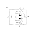
- FIG. 1 is a circuit diagram showing a semiconductor device according to the first embodiment of the present invention.
- FIG. 2 is a perspective view of the semiconductor device shown in FIG.
- FIG. 3 is a plan view of the semiconductor device shown in FIG.
- FIG. 4 is a plan view showing the structure of the semiconductor chip.
- FIG. 5 is a perspective sectional view of a main part showing the structure of the semiconductor chip.
- FIG. 6 is a perspective sectional view of a main part of FIG. 5 excluding the structure on the semiconductor chip.
- FIG. 7 is a plan view of the semiconductor chip shown in FIG.
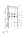
- FIG. 8 is a cross-sectional view taken along the line VIII-VIII shown in FIG.
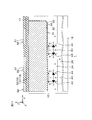
- FIG. 9 is a cross-sectional view taken along the line IX-IX shown in FIG.
- FIG. 1 is a circuit diagram showing a semiconductor device according to the first embodiment of the present invention.
- FIG. 2 is a perspective view of the semiconductor device shown in FIG.
- FIG. 3 is a plan view
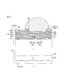
- FIG. 10 is a cross-sectional view taken along the line XX shown in FIG.
- FIG. 11 is a cross-sectional view taken along the line XI-XI shown in FIG.
- FIG. 12 is a schematic cross-sectional view of the structure of the base wiring.
- FIG. 13 is a schematic cross-sectional view of the structure of the gate wiring.
- FIG. 14 is a schematic cross-sectional view of the structure of the first source / drain wiring.
- FIG. 15 is a schematic cross-sectional view of the structure of the second source / drain wiring.
- FIG. 16 is a corresponding diagram of FIG. 5, which is a perspective sectional view of a main part showing a semiconductor device according to a second embodiment of the present invention.
- FIG. 1 is a circuit diagram showing a semiconductor device 1 according to the first embodiment of the present invention.
- the semiconductor device 1 includes a common source drain type MISFET (Metal Insulator Semiconductor Field Effect Transistor) 2.
- the MISFET 2 includes a base B, a gate G, a first source drain SD1 and a second source drain SD2.
- the first source / drain SD1 and the second source / drain SD2 also serve as a source and a drain.
- a reference voltage for example, ground voltage
- a gate voltage VG with reference to the base B is applied to the gate G.
- the gate G controls the conduction and interruption of the current I flowing between the first source-drain SD1 and the second source-drain SD2.
- a first source / drain voltage VSD1 (first voltage) is applied to the first source / drain SD1.
- a second source-drain voltage VSD2 (second voltage) different from the first source-drain voltage VSD1 is applied to the second source-drain SD2.
- the semiconductor device 1 further includes a diode pair 3 connected to the first source / drain SD1 and the second source / drain SD2.
- the diode pair 3 regulates (cuts off) the current I flowing between the first source-drain SD1 and the second source-drain SD2 in the off state of the MISFET2.
- the diode pair 3 includes a first body diode 4 and a second body diode 5 that are reverse-biased to each other.
- the first body diode 4 and the second body diode 5 include an anode and a cathode, respectively.
- the anode of the first body diode 4 is connected to the base B.
- the cathode of the first body diode 4 is connected to the first source / drain SD1.
- the anode of the second body diode 5 is connected to the base B.
- the cathode of the second body diode 5 is connected to the second source drain SD2.
- the semiconductor device 1 is a 4-terminal device including four external terminals 6, 7, 8 and 9.
- the external terminals 6 to 9 include a base terminal 6, a gate terminal 7, a first source / drain terminal 8, and a second source / drain terminal 9.
- the base terminal 6 is connected to the base B.
- the gate terminal 7 is connected to the gate G.
- the first source / drain terminal 8 is connected to the first source / drain SD1.
- the second source / drain terminal 9 is connected to the second source / drain SD2.
- the MISFET 2 is a bidirectional device capable of passing a current I in both directions of the first source / drain terminal 8 and the second source / drain terminal 9. That is, when the first source / drain terminal 8 is connected to the high voltage side (input side), the second source / drain terminal 9 is connected to the low voltage side (output side). On the other hand, when the first source / drain terminal 8 is connected to the low voltage side (output side), the second source / drain terminal 9 is connected to the high voltage side (input side).
- one MISFET 2 can realize the function of a circuit in which the drains of two MISFETs that are not the common source drain type are connected to each other. Therefore, according to the semiconductor device 1, it is possible to reduce the on-resistance by shortening the current path.
- the specific structure of the semiconductor device 1 will be described.
- FIG. 2 is a perspective view of the semiconductor device 1 shown in FIG.
- FIG. 3 is a plan view of the semiconductor device 1 shown in FIG.
- the semiconductor device 1 includes a chip size package having the chip size as the package size
- the semiconductor device 1 includes a rectangular parallelepiped device body 11.
- the device body 11 includes a first device surface 12 on one side, a second device surface 13 on the other side, and device side surfaces 14A, 14B, 14C, 14D connecting the first device surface 12 and the second device surface 13. .
- the device side surfaces 14A to 14D include a first device side surface 14A, a second device side surface 14B, a third device side surface 14C, and a fourth device side surface 14D.
- the first device surface 12 and the second device surface 13 are formed in a quadrangular shape in a plan view (hereinafter, simply referred to as "plan view") viewed from their normal direction Z.
- the first device surface 12 is a connection surface (mounting surface) facing the connection object when connected to the connection object.
- the second device surface 13 is a non-connecting surface (non-mounting surface) on the opposite side of the connecting surface.
- the object to be connected may include a mounting board, an electronic component, a lead frame of a semiconductor package, and the like.
- the first device side surface 14A and the second device side surface 14B extend in the first direction X in a plan view and face the second direction Y intersecting the first direction X.
- the third device side surface 14C and the fourth device side surface 14D extend in the second direction Y in a plan view and face the first direction X.
- the second direction Y is orthogonal to the first direction X.
- the device side surfaces 14A to 14D extend in a plane along the normal direction Z, respectively.
- the device side surfaces 14A to 14D may be ground surfaces having grinding marks.
- the length of the first device side surface 14A (second device side surface 14B) may be 1 mm or more and 5 mm.
- the length of the third device side surface 14C (fourth device side surface 14D) may be 1 mm or more and 5 mm.
- the device body 11 has a laminated structure including a semiconductor chip 15 and an insulating layer 16.
- the semiconductor chip 15 forms a part of the second device surface 13 and the device side surfaces 14A to 14D.
- the insulating layer 16 forms a part of the first device surface 12 and the device side surfaces 14A to 14D.
- the semiconductor chip 15 is made of silicon in this form.
- the semiconductor chip 15 is formed in a rectangular parallelepiped shape.
- the semiconductor chip 15 includes a first main surface 17 on one side, a second main surface 18 on the other side, and side surfaces 19A, 19B, 19C, 19D connecting the first main surface 17 and the second main surface 18.
- the side surfaces 19A to 19D include a first side surface 19A, a second side surface 19B, a third side surface 19C, and a fourth side surface 19D.
- the first main surface 17 and the second main surface 18 are formed in a quadrangular shape in a plan view.
- the first main surface 17 may be a ground surface.
- the second main surface 18 may be a ground surface.
- the second main surface 18 forms the second device surface 13.
- the side surfaces 19A to 19D form a part of the device side surfaces 14A to 14D.
- the insulating layer 16 is formed on the first main surface 17.
- the insulating layer 16 includes an insulating main surface 20 and insulating side surfaces 21A, 21B, 21C, 21D.
- the insulating side surfaces 21A to 21D include a first insulating side surface 21A, a second insulating side surface 21B, a third insulating side surface 21C, and a fourth insulating side surface 21D.
- the insulating main surface 20 extends parallel to the first main surface 17 and is formed in a quadrangular shape in a plan view.
- the insulating main surface 20 forms the first device surface 12.
- the insulating side surfaces 21A to 21D form a part of the device side surfaces 14A to 14D.
- the insulating side surfaces 21A to 21D extend from the peripheral edge of the insulating main surface 20 toward the semiconductor chip 15 and are connected to the side surfaces 19A to 19D. Specifically, the insulating side surfaces 21A to 21D are formed flush with respect to the side surfaces 19A to 19D.
- the plurality of external terminals 6 to 9 are formed on the insulating main surface 20.
- the plurality of external terminals 6 to 9 are arranged in a matrix of 5 rows and 5 columns at intervals in the first direction X and the second direction Y.
- the plurality of external terminals 6 to 9 include, in this embodiment, one base terminal 6, one gate terminal 7, a plurality of first source / drain terminals 8, and a plurality of second source / drain terminals 9.
- the base terminal 6 is arranged in the first column of the third row.
- the gate terminal 7 is arranged in the third row and the fifth column.
- the gate terminal 7 faces the base terminal 6 in the second direction Y.
- the plurality of first source / drain terminals 8 are arranged in the first to fifth columns of the first row and the first to fifth columns of the fourth row.
- the plurality of second source / drain terminals 9 are arranged in the first to fifth columns of the second row and the first to fifth columns of the fifth row.
- the plurality of second source / drain terminals 9 arranged in the second row face the first direction X in a one-to-one correspondence with the plurality of first source / drain terminals 8 arranged in the first row.
- the plurality of second source / drain terminals 9 arranged in the fifth row face the first direction X in a one-to-one correspondence with the plurality of first source / drain terminals 8 arranged in the fourth row. doing.
- any one of the base terminal 6, the gate terminal 7, the first source / drain terminal 8 and the second source / drain terminal 9 may be arranged in each space.
- An electrically open terminal may be arranged in each space.
- the number and arrangement of the base terminal 6, the gate terminal 7, the first source / drain terminal 8 and the second source / drain terminal 9 are all arbitrary, and are not limited to the number and arrangement shown in FIGS. 2 and 3.
- FIG. 4 is a plan view showing the structure of the semiconductor chip 15.
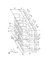
- FIG. 5 is a perspective sectional view of a main part showing the structure of the semiconductor chip 15.
- FIG. 6 is a perspective sectional view of a main part excluding the structure on the semiconductor chip 15 from FIG.
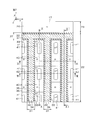
- FIG. 7 is a plan view of the semiconductor chip 15 shown in FIG.
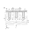
- FIG. 8 is a cross-sectional view taken along the line VIII-VIII shown in FIG.
- FIG. 9 is a cross-sectional view taken along the line IX-IX shown in FIG.
- FIG. 10 is a cross-sectional view taken along the line XX shown in FIG.
- FIG. 11 is a cross-sectional view taken along the line XI-XI shown in FIG.
- the semiconductor chip 15 includes a device region 22 and an outer region 23.
- the device area 22 is also referred to as an active area.
- the device region 22 is a region in which the MISFET 2 is formed.
- the device regions 22 are formed at intervals inward from the side surfaces 19A to 19D in a plan view.
- the device region 22 is formed in a quadrangular shape having four sides parallel to the side surfaces 19A to 19D in a plan view.
- the planar shape of the device region 22 is arbitrary and is not limited to a quadrangular shape.
- the outer region 23 is an region outside the device region 22.
- the outer region 23 extends in a strip shape along the peripheral edge of the device region 22 in a plan view.
- the outer region 23 is formed in an endless shape (in this form, a square ring) surrounding the device region 22 in a plan view.
- the semiconductor device 1 includes an n-type (first conductive type) drift layer 24 formed on the surface layer portion of the first main surface 17 of the semiconductor chip 15.
- the drift layer 24 is formed over the entire surface layer portion of the first main surface 17.
- the drift layer 24 forms a part of the first main surface 17 and the side surfaces 19A to 19D.
- the concentration of n-type impurities in the drift layer 24 may be 1 ⁇ 10 14 cm -3 or more and 1 ⁇ 10 16 cm -3 or less.
- the drift layer 24 has a first thickness T1.
- the first thickness T1 may be 5 ⁇ m or more and 50 ⁇ m or less.
- the first thickness T1 may be 5 ⁇ m or more and 10 ⁇ m or less, 10 ⁇ m or more and 20 ⁇ m or less, 20 ⁇ m or more and 30 ⁇ m or less, 30 ⁇ m or more and 40 ⁇ m or less, or 40 ⁇ m or more and 50 ⁇ m or less.
- the drift layer 24 is composed of an n-type epitaxial layer in this form.
- the semiconductor device 1 includes a p-type (second conductive type) base layer 25 formed in a region on the second main surface 18 side of the semiconductor chip 15 with respect to the drift layer 24.
- the base layer 25 forms the base B of the MISFET 2 (see FIG. 1).
- the base layer 25 is formed over the entire region of the semiconductor chip 15 on the second main surface 18 side, and is electrically connected to the drift layer 24.
- the base layer 25 forms a part of the second main surface 18 and the side surfaces 19A to 19D.
- the concentration of p-type impurities in the base layer 25 may be 1 ⁇ 10 18 cm -3 or more and 1 ⁇ 10 21 cm -3 or less.
- the base layer 25 has a second thickness T2 (T1 ⁇ T2) having a first thickness T1 or more of the drift layer 24.
- the second thickness T2 may be 50 ⁇ m or more and 500 ⁇ m or less.
- the second thickness T2 may be 50 ⁇ m or more and 100 ⁇ m or less, 100 ⁇ m or more and 200 ⁇ m or less, 200 ⁇ m or more and 300 ⁇ m or less, 300 ⁇ m or more and 400 ⁇ m or less, or 400 ⁇ m or more and 500 ⁇ m or less.
- the second thickness T2 preferably exceeds the first thickness T1 (T1 ⁇ T2).
- the base layer 25 is made of a p-type semiconductor substrate.
- the semiconductor device 1 includes at least one (plurality in this embodiment) trench gate structure 31 formed on the first main surface 17 in the device region 22.
- the plurality of trench gate structures 31 are formed in a strip shape extending in the first direction X in a plan view, and are formed at intervals in the second direction Y.
- the plurality of trench gate structures 31 are formed in a striped shape extending in the first direction X in a plan view.
- Each trench gate structure 31 is in contact with the drift layer 24.
- Each trench gate structure 31 is formed at intervals from the bottom of the drift layer 24 to the first main surface 17 side, and faces the base layer 25 with a part of the drift layer 24 interposed therebetween.
- the plurality of trench gate structures 31 are formed with a predetermined pitch PT.
- the pitch PT is the distance between two adjacent trench gate structures 31.
- the pitch PT may be 0.5 ⁇ m or more and 5 ⁇ m or less.
- the pitch PT is 0.5 ⁇ m or more and 1 ⁇ m or less, 1 ⁇ m or more and 1.5 ⁇ m or less, 1.5 ⁇ m or more and 2 ⁇ m or less, 2 ⁇ m or more and 2.5 ⁇ m or less, 2.5 ⁇ m or more and 3 ⁇ m or less, 3 ⁇ m or more and 4 ⁇ m or less, or 4 ⁇ m or more and 5 ⁇ m or less. It may be.
- the plurality of trench gate structures 31 include a gate trench 32, a gate insulating layer 33, and a gate electrode 34, respectively.
- the gate trench 32 is dug down from the first main surface 17 to the second main surface 18.
- the gate trench 32 has a side wall 35 and a bottom wall 36.
- the side wall 35 and the bottom wall 36 may be collectively referred to as an “inner wall”.
- the side wall 35 and the bottom wall 36 are located in the drift layer 24.
- the side wall 35 extends along the normal direction Z.
- the absolute value of the angle formed by the side wall 35 with the first main surface 17 in the semiconductor chip 15 may be 90 ° or more and 95 ° or less (for example, about 91 °).
- the gate trench 32 may be formed in a tapered shape in which the opening width narrows toward the bottom wall 36 side.
- the side wall 35 may be formed perpendicular to the first main surface 17.
- the bottom wall 36 is formed in a curved shape toward the second main surface 18.
- the bottom wall 36 may be formed parallel to the first main surface 17.
- the gate trench 32 may have a depth D of 0.1 ⁇ m or more and 20 ⁇ m or less.
- the depth D is 0.1 ⁇ m or more and 1 ⁇ m or less, 1 ⁇ m or more and 2 ⁇ m or less, 2 ⁇ m or more and 4 ⁇ m or less, 4 ⁇ m or more and 6 ⁇ m or less, 6 ⁇ m or more and 8 ⁇ m or less, 8 ⁇ m or more and 10 ⁇ m or less, 10 ⁇ m or more and 15 ⁇ m or less, or 15 ⁇ m or more and 20 ⁇ m or less. You may.
- the gate trench 32 may have an opening width W of 0.1 ⁇ m or more and 3 ⁇ m or less.
- the opening width W is 0.1 ⁇ m or more and 0.5 ⁇ m or more, 0.5 ⁇ m or more and 1 ⁇ m or less, 1 ⁇ m or more and 1.5 ⁇ m or more, 1.5 ⁇ m or more and 2 ⁇ m or less, 2 ⁇ m or more and 2.5 ⁇ m or more, or 2.5 ⁇ m or more and 3 ⁇ m or less. It may be.
- the opening width W is preferably depth D or less.
- the aspect ratio D / W of the gate trench 32 may be 1 or more and 20 or less.
- the aspect ratio D / W is the ratio of the depth D to the opening width W.
- Aspect ratio D / W is 1 or more 2 or less, 2 or more 4 or less, 4 or more 6 or less, 6 or more 8 or less, 8 or more 10 or less, 10 or more 12 or less, 12 or more 14 or less, 14 or more 16 or less, 16 or more 18 The following, or 18 or more and 20 or less may be used.
- the gate insulating layer 33 is formed in a film shape on the inner wall of the gate trench 32.
- the gate insulating layer 33 contains at least one of silicon oxide, silicon nitride, aluminum oxide, zirconium oxide and tantalum oxide.
- the gate insulating layer 33 is preferably made of silicon oxide.
- the gate insulating layer 33 is formed in the entire inner wall of the gate trench 32, and partitions the recess space in the gate trench 32.
- the gate insulating layer 33 includes an exposed portion exposed from the first main surface 17.
- the exposed portion of the gate insulating layer 33 may be formed flush with the first main surface 17.
- the exposed portion of the gate insulating layer 33 may be a ground surface.
- the thickness of the gate insulating layer 33 may be 10 nm or more and 300 nm or less with respect to the normal direction of the inner wall of the gate trench 32.
- the thickness of the gate insulating layer 33 is 10 nm or more and 25 nm or less, 25 nm or more and 50 nm or less, 50 nm or more and 75 nm or less, 75 nm or more and 100 nm or less, 100 nm or more and 150 nm or less, 150 nm or more and 200 nm or less, 200 nm or more and 250 nm or less, or 250 nm or more and 300 nm or less. It may be.
- the gate electrode 34 is embedded in the gate trench 32 with the gate insulating layer 33 interposed therebetween. Specifically, the gate electrode 34 is embedded in the recess space partitioned by the gate insulating layer 33 in the gate trench 32. The gate electrode 34 forms the gate G of the MISFET 2 (see FIG. 1).
- the gate electrode 34 includes an exposed portion exposed from the first main surface 17.
- the exposed portion of the gate electrode 34 may be formed flush with the first main surface 17.
- the exposed portion of the gate electrode 34 may be a ground surface.
- the gate electrode 34 preferably contains conductive polysilicon.
- the conductive polysilicon may be p-type polysilicon or n-type polysilicon.
- the gate electrode 34 preferably contains n-type polysilicon.
- the gate electrode 34 may contain a metal material such as tungsten (W), copper (Cu), or aluminum (Al).
- the semiconductor device 1 further includes at least one trench contact structure 37 formed on the first main surface 17 at the peripheral edge of the device region 22.
- the semiconductor device 1 includes a plurality of (two in this form) trench contact structures 37.
- One trench contact structure 37 extends in a direction intersecting (specifically, orthogonally) with the plurality of trench gate structures 31 and is connected to one end of the plurality of trench gate structures 31.
- the other trench contact structure 37 extends in a direction intersecting (specifically, orthogonally) with the plurality of trench gate structures 31 and is connected to the other end of the plurality of trench gate structures 31.
- the plurality of trench contact structures 37 include a gate trench 32, a gate insulating layer 33, and a gate electrode 34, respectively.
- the gate trench 32, the gate insulating layer 33, and the gate electrode 34 of the trench contact structure 37 are integrally formed with the gate trench 32, the gate insulating layer 33, and the gate electrode 34 of the trench gate structure 31, respectively.
- the plurality of trench contact structures 37 form a plurality of annular trench gate structures 31 having a portion extending in the first direction X and a portion extending in the second direction Y.
- the plurality of annular trench gate structures 31 are connected to each other so that the portions extending in the first direction X are integrated with each other.
- the plurality of trench contact structures 37 can be regarded as forming portions extending in the second direction Y of the annular trench gate structure 31.
- one ladder-shaped trench gate structure 31 is formed in a plan view.
- the semiconductor device 1 includes at least one (s) of p-type channel regions 40 formed in the drift layer 24 so as to cover the side wall 35 of the trench gate structure 31.
- Each channel region 40 forms a channel CH of the MISFET 2 in a portion along the side wall 35 of the trench gate structure 31.
- the p-type impurity concentration in the channel region 40 may be 1 ⁇ 10 14 cm -3 or more and 1 ⁇ 10 18 cm -3 or less.
- the plurality of channel regions 40 are formed at intervals in the first direction X in a plan view, and are formed in a band shape extending in the second direction Y, respectively.
- the plurality of channel regions 40 are formed in a striped shape extending in the second direction Y in a plan view.
- the plurality of channel regions 40 intersect (specifically, orthogonally) the plurality of trench gate structures 31.
- the plurality of channel regions 40 are formed at intervals in the first direction X in the region between two trench gate structures 31 adjacent to each other.
- Each channel region 40 extends from the first main surface 17 toward the bottom of the drift layer 24, and has a bottom portion located on the bottom side of the drift layer 24 with respect to the bottom wall 36 of the trench gate structure 31.
- the bottom of each channel region 40 is connected to the base layer 25 in this form.
- each channel region 40 is electrically connected to the base layer 25. That is, a reference voltage is applied to the channel region 40 via the base layer 25.
- Each channel region 40 further covers the bottom wall 36 of the trench gate structure 31.
- Each channel region 40 forms a channel CH of the MISFET 2 in a portion along the bottom wall 36 of the trench gate structure 31.
- the channel length of the channel CH is increased by increasing the area of the side wall 35 of the trench gate structure 31. Therefore, deeply forming the trench gate structure 31 is effective in increasing the channel length of the MISFET 2.
- Each channel region 40 is formed by introducing p-type impurities into the drift layer 24.
- Each channel region 40 may have a trench formed in the drift layer 24 and a trench structure including p-type polysilicon embedded in the trench.
- the semiconductor device 1 includes an n + type first source / drain region 41 and an n + type second source / drain region 42 formed in the drift layer 24.
- the first source / drain region 41 and the second source / drain region 42 are each composed of a region in which the source region and the drain region are integrated.
- the first source / drain region 41 forms the first source / drain SD1 of the MISFET 2 (see FIG. 1).
- the second source / drain region 42 forms the second source / drain SD2 of the MISFET 2 (see FIG. 1).
- the first source / drain region 41 and the second source / drain region 42 each have an n-type impurity concentration that exceeds the n-type impurity concentration of the drift layer 24.
- the concentration of n-type impurities in the first source / drain region 41 may be 1 ⁇ 10 18 cm -3 or more and 1 ⁇ 10 21 cm -3 or less.
- the concentration of n-type impurities in the second source / drain region 42 may be 1 ⁇ 10 18 cm -3 or more and 1 ⁇ 10 21 cm -3 or less.
- the n-type impurity concentration in the second source-drain region 42 is preferably equal to the n-type impurity concentration in the first source-drain region 41.
- the first source / drain region 41 and the second source / drain region 42 are formed in the drift layer 24 at intervals along the side wall 35 of the trench gate structure 31 so as to face each other with the channel region 40 in between.
- a plurality of first source / drain regions 41 and a plurality of second source / drain regions 42 are formed in the drift layer 24.
- the plurality of first source / drain regions 41 are formed at intervals in the first direction X in the region between two adjacent trench gate structures 31.
- the plurality of first source / drain regions 41 face each other in the second direction Y with the trench gate structure 31 interposed therebetween. That is, the plurality of first source / drain regions 41 are formed at intervals in the second direction Y in such a manner that they are arranged alternately with the plurality of trench gate structures 31 with respect to the second direction Y.
- the plurality of first source / drain regions 41 are arranged in a matrix in a plan view with an interval in the first direction X and the second direction Y.
- Each first source / drain region 41 is formed at intervals from each channel region 40, and faces each channel region 40 with a part of the drift layer 24 interposed therebetween.
- Each first source / drain region 41 is formed at intervals from each trench gate structure 31 and faces each trench gate structure 31 with a part of the drift layer 24 interposed therebetween.
- each first source / drain region 41 is formed in a region on the first main surface 17 side with respect to the bottom of the drift layer 24.
- the bottom of each first source / drain region 41 may be formed at a depth between the bottom of the drift layer 24 and the bottom wall 36 of the trench gate structure 31.
- the bottom of each first source / drain region 41 may be formed at a depth position between the first main surface 17 and the bottom wall 36 of the trench gate structure 31. From the viewpoint of increasing the channel length of the channel CH, it is preferable that each first source / drain region 41 is formed with a thickness that crosses at least an intermediate portion of each trench gate structure 31.
- the plurality of second source / drain regions 42 are formed at intervals in the first direction X in the region between two adjacent trench gate structures 31. Specifically, the plurality of second source / drain regions 42 are formed alternately with the plurality of first source / drain regions 41 at intervals in the first direction X so as to sandwich one channel region 40.
- the plurality of second source / drain regions 42 face each other in the second direction Y with the trench gate structure 31 interposed therebetween. That is, the plurality of second source / drain regions 42 are formed at intervals in the second direction Y in such a manner that they are arranged alternately with the plurality of trench gate structures 31. As a result, the plurality of second source / drain regions 42 are arranged in a matrix in a plan view with an interval in the first direction X and the second direction Y.
- Each second source / drain region 42 is formed at intervals from each channel region 40, and faces each channel region 40 with a part of the drift layer 24 interposed therebetween.
- Each second source / drain region 42 is formed at intervals from each trench gate structure 31 and faces each trench gate structure 31 with a part of the drift layer 24 interposed therebetween.
- each second source / drain region 42 is formed in a region on the first main surface 17 side with respect to the bottom of the drift layer 24.
- the bottom of each second source / drain region 42 may be formed at a depth between the bottom of the drift layer 24 and the bottom wall 36 of the trench gate structure 31.
- the bottom of each second source / drain region 42 may be formed at a depth position between the first main surface 17 and the bottom wall 36 of the trench gate structure 31.
- each second source / drain region 42 is formed with a thickness that crosses at least the intermediate portion of each trench gate structure 31.
- Each second source / drain region 42 is preferably formed to have a thickness equal to the thickness of each first source / drain region 41.
- the semiconductor device 1 includes a first pn junction 43.
- the first pn junction 43 forms the first body diode 4 of the MISFET 2.
- the first pn junction 43 is formed in the region between the channel region 40 and the first source / drain region 41.
- the first pin junction 43 has a first pin junction (p-intrinsic-n junction portion) having a channel region 40 as a P layer, a drift layer 24 as an I layer (Intrinsic layer), and a first source / drain region 41 as an N layer. ) May be.
- the semiconductor device 1 includes a second pn junction 44.
- the second pn junction 44 forms the second body diode 5 of the MISFET 2. That is, the second pn junction 44 forms a diode pair 3 with the first pn junction 43.
- the second pn junction 44 is formed in the region between the channel region 40 and the second source / drain region 42.
- the second pn junction 44 is reverse-biased to the first pn junction 43 via the channel region 40.
- the second pin junction 44 may be a second pin junction having a channel region 40 as a P layer, a drift layer 24 as an I layer, and a second source / drain region 42 as an N layer.
- the channel region 40, the plurality of first source / drain regions 41, and the plurality of second source / drain regions 42 are formed in the regions partitioned by the annular trench gate structure 31, respectively.
- the channel CH of the MISFET 2 can be formed in the region partitioned by the annular trench gate structure 31. Therefore, since the current path of the MISFET 2 can be limited to the region partitioned by the annular trench gate structure 31, the leakage current can be suppressed.
- FIG. 12 is a schematic cross-sectional view of the structure of the base wiring 56.
- FIG. 13 is a schematic cross-sectional view of the structure of the gate wiring 57.
- FIG. 14 is a schematic cross-sectional view of the structure of the first source / drain wiring 58.
- FIG. 15 is a schematic cross-sectional view of the structure of the second source / drain wiring 59. 12 to 15 do not show a cross section of a specific portion in the semiconductor device 1.
- the insulating layer 16 has a laminated structure in which a plurality of insulating layers are laminated.
- the number of layers of the insulating layer is arbitrary and is not limited to a specific number of layers.
- the insulating layer 16 includes a first insulating layer 51, a second insulating layer 52, a third insulating layer 53, a fourth insulating layer 54, and a fifth insulating layer 55.
- the first to fourth insulating layers 51 to 54 preferably contain an inorganic insulator.
- the first to fourth insulating layers 51 to 54 may contain silicon oxide or silicon nitride.
- the first to third insulating layers 51 to 53 each contain silicon oxide in this form.
- the fourth insulating layer 54 preferably contains an insulating material different from that of the first to third insulating layers 51 to 53.
- the fourth insulating layer 54 contains silicon nitride in this form.
- the uppermost fifth insulating layer 55 preferably contains an insulating material different from that of the first to fourth insulating layers 51 to 54.
- the uppermost fifth insulating layer 55 preferably contains an organic insulator.
- the fifth insulating layer 55 may contain polyimide, polyamide or polybenzoxazole as an example of an organic insulator.
- the fourth insulating layer 54 and the fifth insulating layer 55 form the uppermost layer of the insulating layer 16 and are formed as a protective layer against the lower layer structure.
- the fourth insulating layer 54 is also referred to as a passivation layer.
- the semiconductor device 1 includes a base wiring 56, a gate wiring 57, a first source / drain wiring 58, and a second source / drain wiring 59 formed in the insulating layer 16.
- the base wiring 56 is selectively routed in the insulating layer 16 to electrically connect the base terminal 6 and the channel region 40 (base layer 25).
- the base wiring 56 transmits the reference voltage (for example, the ground voltage) applied to the base terminal 6 to the base layer 25 and the channel region 40.
- the base wiring 56 includes a first lower wiring 61, a first intermediate wiring 62, a first upper wiring 63, a first lower via electrode 64, and a first upper via electrode 65.
- the first lower wiring 61 is selectively formed on the first insulating layer 51.
- the first intermediate wiring 62 is selectively formed on the second insulating layer 52.
- the first upper wiring 63 is selectively formed on the third insulating layer 53.
- the first lower wiring 61, the first intermediate wiring 62, and the first upper wiring 63 may include at least one of a pure Al layer, a pure Cu layer, an AlCu layer, an AlSi layer, and an AlSiCu layer, respectively.
- the first lower via electrode 64 is embedded in the first insulating layer 51, and electrically connects an arbitrary region of the channel region 40 and the first lower wiring 61.
- a plurality of first lower via electrodes 64 may be connected to the channel region 40 in any region of the semiconductor chip 15. For example, if part of the channel region 40 is pulled out to the outer region 23, one or more first lower via electrodes 64 are electrically connected to the channel region 40 (base layer 25) in the outer region 23. You may be.
- the first lower via electrode 64 includes a main body layer 66 and a barrier layer 67.
- the main body layer 66 is embedded in the first insulating layer 51.
- the main body layer 66 may include a W layer or a Cu layer.
- the barrier layer 67 is interposed between the first insulating layer 51 and the main body layer 66.
- the barrier layer 67 may include at least one of a Ti layer and a TiN layer.
- the first upper via electrode 65 is embedded in the second insulating layer 52, and electrically connects an arbitrary region of the first intermediate wiring 62 and an arbitrary region of the first upper wiring 63.
- the first upper via electrode 65 includes a main body layer 66 and a barrier layer 67, similarly to the first lower via electrode 64.
- the gate wiring 57 is selectively routed in the insulating layer 16 to electrically connect the gate terminal 7 and the gate electrode 34.
- the gate wiring 57 transmits the gate voltage VG applied to the gate terminal 7 to the gate electrode 34.
- the gate wiring 57 includes a second lower wiring 71, a second intermediate wiring 72, a second upper wiring 73, a second lower via electrode 74, and a second upper via electrode 75.
- the second lower wiring 71 is selectively formed on the first insulating layer 51.
- the second intermediate wiring 72 is selectively formed on the second insulating layer 52.
- the second upper wiring 73 is selectively formed on the third insulating layer 53.
- the second lower wiring 71, the second intermediate wiring 72, and the second upper wiring 73 may include at least one of a pure Al layer, a pure Cu layer, an AlCu layer, an AlSi layer, and an AlSiCu layer, respectively.
- the second lower via electrode 74 is embedded in the first insulating layer 51 and electrically connects the gate electrode 34 and the second lower wiring 71.
- the second lower via electrode 74 is electrically connected to the gate electrode 34 of the trench contact structure 37.
- the second lower via electrode 74 may be electrically connected to the gate electrode 34 of the trench gate structure 31.
- FIG. 13 shows an example in which a plurality of second lower via electrodes 74 are connected to the gate electrode 34 of the trench gate structure 31 for convenience of explanation.
- the second lower via electrode 74 includes a main body layer 66 and a barrier layer 67 like the first lower via electrode 64.
- the second upper via electrode 75 is embedded in the second insulating layer 52, and electrically connects an arbitrary region of the second intermediate wiring 72 and an arbitrary region of the second upper wiring 73.
- the second upper via electrode 75 includes a main body layer 66 and a barrier layer 67 like the second lower via electrode 74.
- the first source / drain wiring 58 is selectively routed in the insulating layer 16 to electrically connect the first source / drain terminal 8 and the first source / drain region 41.
- the first source / drain wiring 58 transmits the current I from the first source / drain terminal 8 to the first source / drain region 41, or transmits the current I from the first source / drain region 41 to the first source / drain terminal 8.
- the first source / drain wiring 58 includes a third lower wiring 81, a third intermediate wiring 82, a third upper wiring 83, a third lower via electrode 84, and a third upper via electrode 85.
- the third lower wiring 81 is selectively formed on the first insulating layer 51.
- the third intermediate wiring 82 is selectively formed on the second insulating layer 52.
- the third upper wiring 83 is selectively formed on the third insulating layer 53.
- the third lower wiring 81, the third intermediate wiring 82, and the third upper wiring 83 may include at least one of a pure Al layer, a pure Cu layer, an AlCu layer, an AlSi layer, and an AlSiCu layer, respectively.
- the third lower via electrode 84 is embedded in the first insulating layer 51, and electrically connects the first source / drain region 41 and the third lower wiring 81.
- the plurality of third lower via electrodes 84 are electrically connected to the corresponding first source / drain regions 41, respectively.
- the third lower via electrode 84 includes a main body layer 66 and a barrier layer 67 like the first lower via electrode 64.
- the third upper via electrode 85 is embedded in the second insulating layer 52, and electrically connects an arbitrary region of the third intermediate wiring 82 and an arbitrary region of the third upper wiring 83.
- the third upper via electrode 85 includes a main body layer 66 and a barrier layer 67 like the third lower via electrode 84.
- the first source / drain wiring 58 may include a plurality of third lower wirings 81.
- the plurality of third lower wirings 81 are formed at intervals in the first direction X, and are formed in a strip shape extending in the second direction Y so as to cross the plurality of trench gate structures 31.
- Each third lower wiring 81 is formed on a plurality of first source / drain regions 41.
- Each third lower wiring 81 is electrically connected to a plurality of first source / drain regions 41 located directly below the third lower wiring 81.
- the second source / drain wiring 59 is selectively routed in the insulating layer 16 to electrically connect the second source / drain terminal 9 and the second source / drain region 42.
- the second source / drain wiring 59 transmits the current I from the second source / drain terminal 9 to the second source / drain region 42, or transmits the current I from the second source / drain region 42 to the second source / drain terminal 9.
- the second source / drain wiring 59 includes a fourth lower wiring 91, a fourth intermediate wiring 92, a fourth upper wiring 93, a fourth lower via electrode 94, and a fourth upper via electrode 95.
- the fourth lower wiring 91 is selectively formed on the first insulating layer 51.
- the fourth intermediate wiring 92 is selectively formed on the second insulating layer 52.
- the fourth upper wiring 93 is selectively formed on the third insulating layer 53.
- the fourth lower wiring 91, the fourth intermediate wiring 92, and the fourth upper wiring 93 may include at least one of a pure Al layer, a pure Cu layer, an AlCu layer, an AlSi layer, and an AlSiCu layer, respectively.
- the fourth lower via electrode 94 is embedded in the first insulating layer 51 and electrically connects the second source / drain region 42 and the fourth lower wiring 91.
- the plurality of fourth lower via electrodes 94 are electrically connected to the corresponding second source / drain regions 42, respectively.
- the fourth lower via electrode 94 includes a main body layer 66 and a barrier layer 67 like the first lower via electrode 64.
- the fourth upper via electrode 95 is embedded in the second insulating layer 52, and electrically connects an arbitrary region of the fourth intermediate wiring 92 and an arbitrary region of the fourth upper wiring 93.
- the fourth upper via electrode 95 includes a main body layer 66 and a barrier layer 67 like the fourth lower via electrode 94.
- the second source / drain wiring 59 may include a plurality of fourth lower wiring 91.
- the plurality of fourth lower wiring 91s are formed at intervals in the first direction X, and are formed in a strip shape extending in the second direction Y so as to cross the plurality of trench gate structures 31.
- the plurality of fourth lower wirings 91 are arranged along the plurality of third lower wirings 81 and the first direction X of the first source / drain wiring 58 according to the arrangement of the first source / drain area 41 and the second source / drain area 42. It is formed in an alternating arrangement.
- Each fourth lower wiring 91 is formed on a plurality of second source / drain regions 42.
- Each of the fourth lower wiring 91 is electrically connected to a plurality of second source / drain regions 42 located directly below the fourth lower wiring 91.
- the base terminal 6, the gate terminal 7, the first source / drain terminal 8 and the second source / drain terminal 9 are formed on the fifth insulating layer 55, respectively.
- the base terminal 6, the gate terminal 7, the first source / drain terminal 8 and the second source / drain terminal 9 penetrate a part of the insulating layer 16 (the fourth insulating layer 54 and the fifth insulating layer 55).
- the base terminal 6 is electrically connected to the first upper wiring 63 of the base wiring 56.
- the gate terminal 7 is electrically connected to the second upper wiring 73 of the gate wiring 57.
- the first source / drain terminal 8 is electrically connected to the third upper wiring 83 of the first source / drain wiring 58.
- the second source / drain terminal 9 is electrically connected to the fourth upper wiring 93 of the second source / drain wiring 59.
- the base terminal 6, the gate terminal 7, the first source / drain terminal 8 and the second source / drain terminal 9 include a base electrode layer 96 and a low melting point metal layer 97, respectively.
- the base electrode layer 96 is formed in the pad opening 98 that penetrates a part of the insulating layer 16 (the fourth insulating layer 54 and the fifth insulating layer 55).
- the base electrode layer 96 includes an overlapping portion drawn from the pad opening 98 to the insulating main surface 20 of the insulating layer 16.
- the base electrode layer 96 may include at least one of a Ti layer, a TiN layer, a Cu layer, an Au layer, a Ni layer, and an Al layer.
- the low melting point metal layer 97 is formed on the base electrode layer 96.
- the low melting point metal layer 97 covers the overlapping portion of the base electrode layer 96.
- the low melting point metal layer 97 projects hemispherically from the main insulating surface 20.
- the low melting point metal layer 97 may contain solder.
- the semiconductor device 1 includes the semiconductor chip 15, the drift layer 24, the trench gate structure 31, the channel region 40, the first source / drain region 41, and the second source / drain region 42.
- the drift layer 24 is formed on the surface layer portion of the first main surface 17 of the semiconductor chip 15.
- the trench gate structure 31 is formed on the first main surface 17 so as to be in contact with the drift layer 24.
- the channel region 40 is formed in the drift layer 24 so as to cover the side wall 35 of the trench gate structure 31.
- the first source / drain region 41 and the second source / drain region 42 are formed in the drift layer 24 at intervals along the side wall 35 of the trench gate structure 31 so as to face each other with the channel region 40 interposed therebetween. ..
- the channel CH of the MISFET 2 is formed in the region along the side wall 35 of the trench gate structure 31.
- an electric current can flow along the side wall 35 of the trench gate structure 31. Therefore, since the current path can be increased, the current capacity can be improved.
- the channel region 40 further covers the bottom wall 36 of the trench gate structure 31.
- the channel CH of the MISFET 2 is also formed in the region along the bottom wall 36 of the trench gate structure 31. Thereby, the current capacity can be further improved.
- FIG. 16 is a corresponding diagram of FIG. 5, and is a perspective sectional view of a main part showing the semiconductor device 101 according to the second embodiment of the present invention.
- the semiconductor device 1 includes a first source / drain region 41 and a second source / drain region 42, which are composed of impurity regions, respectively.
- the semiconductor device 101 includes a first source / drain region 41 and a second source / drain region 42, which are made of a metal material instead of the impurity region.
- the same reference numerals will be given to the structures corresponding to the structures described for the semiconductor device 1, and the description thereof will be omitted.
- the first source / drain region 41 and the second source / drain region 42 have a trench electrode structure including a trench 102 and a metal electrode 103, respectively.
- the trench 102 is formed by digging the first main surface 17 toward the second main surface 18.
- the trench 102 exposes the drift layer 24.
- the bottom of the trench 102 is formed in a region on the first main surface 17 side with respect to the bottom of the drift layer 24.
- the bottom of the trench 102 may be formed at a depth position between the bottom of the drift layer 24 and the bottom wall 36 of the trench gate structure 31.
- the bottom of the trench 102 may be formed at a depth position between the first main surface 17 and the bottom wall 36 of the trench gate structure 31.
- the trench 102 is preferably formed with a thickness that crosses at least the intermediate portion of each trench gate structure 31.
- the metal electrode 103 is embedded in the trench 102.
- the metal electrode 103 is electrically connected to the drift layer 24 in the trench 102.
- the metal electrode 103 may include a main body layer 104 and a barrier layer 105.
- the main body layer 104 is embedded in the trench 102.
- the main body layer 104 may include at least one of a W layer, a pure Al layer, a pure Cu layer, an AlCu layer, an AlSi layer, and an AlSiCu layer, respectively.
- the barrier layer 105 is interposed between the drift layer 24 and the main body layer 104.
- the barrier layer 105 may include at least one of a Ti layer and a TiN layer.
- the first source / drain region 41 may also serve as the third lower via electrode 84 according to the first embodiment.
- the second source / drain region 42 may also serve as the fourth lower via electrode 94 according to the first embodiment.
- the semiconductor device 101 can also exert the same effect as the effect described for the semiconductor device 1.
- the present invention can be implemented in still other forms.
- the first conductive type is n type and the second conductive type is p type
- the first conductive type may be p type
- the second conductive type may be n type.
- the specific configuration in this case can be obtained by replacing the n-type region with the p-type region and replacing the p-type region with the n-type region in the above description and the accompanying drawings.
- the semiconductor chip 15 made of silicon is adopted in each of the above-described embodiments.
- the semiconductor chip 15 made of a wide bandgap semiconductor may be adopted in each of the above-described embodiments.
- the semiconductor chip 15 may be made of SiC (silicon carbide) as an example of a wide bandgap semiconductor.
- the semiconductor chip 15 may be made of a SiC single crystal composed of hexagonal crystals.
- the SiC single crystal composed of hexagonal crystals has a plurality of polytypes including 2H (Hexagonal) -SiC single crystal, 4H-SiC single crystal and 6H-SiC single crystal, depending on the period of the atomic arrangement.
- the semiconductor chip 15 is preferably made of a 4H-SiC single crystal among a plurality of types of polytypes.
- the first main surface 17 is formed by the (0001) plane (silicon surface) of the SiC single crystal
- the second main surface 18 is formed by the (000-1) plane (carbon surface) of the SiC single crystal.
- the first main surface 17 may be formed by the (000-1) surface
- the second main surface 18 may be formed by the (0001) surface.
- the (0001) and (000-1) planes of a SiC single crystal are referred to as the c-plane.
- the normal direction Z of the c-plane of the SiC single crystal is referred to as the c-axis ([0001] direction).
- the first main surface 17 may have an off angle inclined at a predetermined angle in a predetermined off direction with respect to the c surface of the SiC single crystal.
- the off direction is preferably the [11-20] direction of the SiC single crystal.
- the off angle may be 0 ° or more and 10 ° or less.
- the off angle is preferably 0 ° or more and 5.0 ° or less.
- the off angle is 0 ° or more and 1.0 ° or less, 1.0 ° or more and 2.0 ° or less, 2.0 ° or more and 3.0 ° or less, 3.0 ° or more and 4.0 ° or less, or 4. It may be set in an angle range of 0 ° or more and 5.0 ° or less.
- the plurality of trench gate structures 31 are formed in a band shape extending along the m-axis direction of the SiC single crystal, and are formed at intervals in the a-axis direction of the SiC single crystal.
- the plurality of trench gate structures 31 may be formed in strips extending along the a-axis direction of the SiC single crystal, and may be formed at intervals in the m-axis direction of the SiC single crystal.
- the m-axis direction is the [1-100] direction and the [-1100] direction of the SiC single crystal.
- the a-axis direction is the [11-20] direction and the [-1-120] direction of the SiC single crystal.
- the semiconductor devices 1 and 101 are composed of a chip size package.
- the semiconductor devices 1 and 101 do not necessarily have to consist of a chip size package.
- the semiconductor devices 1, 101 may be redesigned to an appropriate form so that they can be incorporated into various semiconductor packages.
- Semiconductor packages include SOP (Small Outline Package), TO (Transistor Outline), QFN (Quad For Non Lead Package), DFP (Dual Flat Package), DIP (Dual Inline Package), QFP (Quad Flat Package), SIP (Quad Flat Package). Single Inline Package), SOJ (Small Outline J-leaded Package), or various forms similar to these are exemplified.
- a semiconductor chip having a main surface, a first conductive type drift layer formed on the surface layer portion of the main surface, a trench gate structure formed on the main surface so as to be in contact with the drift layer, and the above.
- a second conductive type channel region formed in the drift layer so as to cover the side wall of the trench gate structure and the drift layer along the side wall of the trench gate structure so as to face each other across the channel region.
- a semiconductor device including a first source-drain region and a second source-drain region formed at intervals in the regions.
- a first pn junction formed in a region between the channel region and the first source / drain region, and a region between the channel region and the second source / drain region are formed through the channel region.
- the trench gate structure extends in a strip shape in a plan view, and a plurality of the channel regions are formed at intervals along the trench gate structure, and a plurality of the first source / drain regions and a plurality of the first source / drain regions are formed. 2. The semiconductor device according to any one of A1 to A6, wherein the source / drain regions are alternately formed along the trench gate structure so as to sandwich one of the channel regions.
- a plurality of the trench gate structures are formed at intervals, and the channel region, the first source / drain region, and the second source / drain region are located in a region between the plurality of trench gate structures.
- the trench gate structure is formed in an annular shape in a plan view, and the channel region, the first source / drain region, and the second source / drain region are formed in a region surrounded by the trench gate structure.
- the semiconductor device according to any one of A1 to A8.
- A20 The semiconductor device according to any one of A1 to A19, which comprises a chip size package.
Landscapes
- Metal-Oxide And Bipolar Metal-Oxide Semiconductor Integrated Circuits (AREA)
- Insulated Gate Type Field-Effect Transistor (AREA)
- Electrodes Of Semiconductors (AREA)
- Internal Circuitry In Semiconductor Integrated Circuit Devices (AREA)
- Semiconductor Integrated Circuits (AREA)
Abstract
Description
6 ベース端子
7 ゲート端子
8 第1ソースドレイン端子
9 第2ソースドレイン端子
11 デバイス本体
15 半導体チップ
16 絶縁層
17 第1主面
19A 第1側面
19B 第2側面
19C 第3側面
19D 第4側面
20 絶縁主面
21A 第1絶縁側面
21B 第2絶縁側面
21C 第3絶縁側面
21D 第4絶縁側面
24 ドリフト層
31 トレンチゲート構造
35 側壁
36 底壁
40 チャネル領域
41 第1ソースドレイン領域
42 第2ソースドレイン領域
43 第1pn接合部
44 第2pn接合部
101 半導体装置
Claims (20)
- 主面を有する半導体チップと、
前記主面の表層部に形成された第1導電型のドリフト層と、
前記ドリフト層に接するように前記主面に形成されたトレンチゲート構造と、
前記トレンチゲート構造の側壁を被覆するように前記ドリフト層に形成された第2導電型のチャネル領域と、
前記チャネル領域を挟んで互いに対向するように、前記ドリフト層において前記トレンチゲート構造の側壁に沿う領域に間隔を空けて形成された第1ソースドレイン領域および第2ソースドレイン領域と、を含む、半導体装置。 - 前記チャネル領域は、前記トレンチゲート構造の底壁をさらに被覆している、請求項1に記載の半導体装置。
- 前記チャネル領域および前記第1ソースドレイン領域の間の領域に形成された第1pn接合部と、
前記チャネル領域および前記第2ソースドレイン領域の間の領域に形成され、前記チャネル領域を介して前記第1pn接合部に逆バイアス接続された第2pn接合部と、をさらに含む、請求項1または2に記載の半導体装置。 - 前記第1ソースドレイン領域および前記第2ソースドレイン領域は、前記チャネル領域から間隔を空けて形成されている、請求項1~3のいずれか一項に記載の半導体装置。
- 前記第1ソースドレイン領域および前記第2ソースドレイン領域は、前記トレンチゲート構造から間隔を空けて形成されている、請求項1~4のいずれか一項に記載の半導体装置。
- 前記チャネル領域は、前記トレンチゲート構造に交差している、請求項1~5のいずれか一項に記載の半導体装置。
- 前記トレンチゲート構造は、平面視において帯状に延び、
複数の前記チャネル領域が、前記トレンチゲート構造に沿って間隔を空けて形成され、
複数の前記第1ソースドレイン領域および複数の前記第2ソースドレイン領域が、1つの前記チャネル領域を挟み込む態様で前記トレンチゲート構造に沿って交互に形成されている、請求項1~6のいずれか一項に記載の半導体装置。 - 複数の前記トレンチゲート構造が、間隔を空けて形成されており、
前記チャネル領域、前記第1ソースドレイン領域および前記第2ソースドレイン領域は、複数の前記トレンチゲート構造の間の領域に形成されている、請求項1~7のいずれか一項に記載の半導体装置。 - 前記トレンチゲート構造は、平面視において環状に形成されており、
前記チャネル領域、前記第1ソースドレイン領域および前記第2ソースドレイン領域は、前記トレンチゲート構造に取り囲まれた領域内に形成されている、請求項1~8のいずれか一項に記載の半導体装置。 - 第1電圧が前記第1ソースドレイン領域に印加され、
前記第1電圧とは異なる第2電圧が前記第2ソースドレイン領域に印加される、請求項1~9のいずれか一項に記載の半導体装置。 - 基準電圧が前記チャネル領域に印加される、請求項1~10のいずれか一項に記載の半導体装置。
- 前記主面の上に形成され、前記トレンチゲート構造に導通する第1端子と、
前記主面の上に形成され、前記チャネル領域に導通する第2端子と、
前記主面の上に形成され、前記第1ソースドレイン領域に導通する第3端子と、
前記主面の上に形成され、前記第2ソースドレイン領域に導通する第4端子と、をさらに含む、請求項1~11のいずれか一項に記載の半導体装置。 - 前記主面を被覆する絶縁層をさらに含み、
前記第1端子、前記第2端子、前記第3端子および前記第4端子は、前記絶縁層の上に形成されている、請求項12に記載の半導体装置。 - 前記絶縁層内に形成され、前記トレンチゲート構造および前記第1端子に導通する第1配線と、
前記絶縁層内に形成され、前記チャネル領域および前記第2端子に導通する第2配線と、
前記絶縁層内に形成され、前記第1ソースドレイン領域および前記第3端子に導通する第3配線と、
前記絶縁層内に形成され、前記第2ソースドレイン領域および前記第4端子に導通する第4配線と、をさらに含む、請求項13に記載の半導体装置。 - 前記半導体チップは、側面を有しており、
前記絶縁層は、前記側面に連なる絶縁側面を有している、請求項13または14に記載の半導体装置。 - 前記ドリフト層は、エピタキシャル層によって形成されている、請求項1~15のいずれか一項に記載の半導体装置。
- 前記第1ソースドレイン領域および前記第2ソースドレイン領域は、第1導電型の不純物領域からそれぞれなる、請求項1~16のいずれか一項に記載の半導体装置。
- 前記第1ソースドレイン領域および前記第2ソースドレイン領域は、金属材料からそれぞれなる、請求項1~16のいずれか一項に記載の半導体装置。
- 前記半導体チップは、シリコンまたは炭化シリコンからなる、請求項1~18のいずれか一項に記載の半導体装置。
- チップサイズパッケージからなる、請求項1~19のいずれか一項に記載の半導体装置。
Priority Applications (4)
| Application Number | Priority Date | Filing Date | Title |
|---|---|---|---|
| JP2021551198A JP7588083B2 (ja) | 2019-09-30 | 2020-09-25 | 半導体装置 |
| DE112020004667.2T DE112020004667T5 (de) | 2019-09-30 | 2020-09-25 | Halbleiterbauteil |
| CN202080069132.3A CN114503278A (zh) | 2019-09-30 | 2020-09-25 | 半导体装置 |
| US17/640,241 US12278268B2 (en) | 2019-09-30 | 2020-09-25 | Semiconductor device |
Applications Claiming Priority (2)
| Application Number | Priority Date | Filing Date | Title |
|---|---|---|---|
| JP2019-180862 | 2019-09-30 | ||
| JP2019180862 | 2019-09-30 |
Publications (1)
| Publication Number | Publication Date |
|---|---|
| WO2021065740A1 true WO2021065740A1 (ja) | 2021-04-08 |
Family
ID=75336463
Family Applications (1)
| Application Number | Title | Priority Date | Filing Date |
|---|---|---|---|
| PCT/JP2020/036385 Ceased WO2021065740A1 (ja) | 2019-09-30 | 2020-09-25 | 半導体装置 |
Country Status (5)
| Country | Link |
|---|---|
| US (1) | US12278268B2 (ja) |
| JP (1) | JP7588083B2 (ja) |
| CN (1) | CN114503278A (ja) |
| DE (1) | DE112020004667T5 (ja) |
| WO (1) | WO2021065740A1 (ja) |
Families Citing this family (1)
| Publication number | Priority date | Publication date | Assignee | Title |
|---|---|---|---|---|
| CN118077057B (zh) * | 2022-09-23 | 2025-11-21 | 华为数字能源技术有限公司 | 半导体器件、其制备方法、功率转换电路及车辆 |
Citations (4)
| Publication number | Priority date | Publication date | Assignee | Title |
|---|---|---|---|---|
| JPH08264764A (ja) * | 1995-03-22 | 1996-10-11 | Toshiba Corp | 半導体装置 |
| JP2006100824A (ja) * | 2004-09-29 | 2006-04-13 | Agere Systems Inc | トレンチ拡散領域を有する金属酸化物半導体デバイスおよびその形成方法 |
| JP2012004541A (ja) * | 2010-05-19 | 2012-01-05 | Renesas Electronics Corp | 半導体装置およびその製造方法 |
| JP2013247127A (ja) * | 2012-05-23 | 2013-12-09 | Renesas Electronics Corp | トランジスタ及びその製造方法 |
Family Cites Families (13)
| Publication number | Priority date | Publication date | Assignee | Title |
|---|---|---|---|---|
| EP1786031A1 (en) * | 2005-11-10 | 2007-05-16 | STMicroelectronics S.r.l. | Vertical-gate mos transistor for high voltage applications with variable gate oxide thickness |
| JP6021246B2 (ja) * | 2012-05-09 | 2016-11-09 | ローム株式会社 | 半導体装置およびその製造方法 |
| US8669611B2 (en) * | 2012-07-11 | 2014-03-11 | Taiwan Semiconductor Manufacturing Company, Ltd. | Apparatus and method for power MOS transistor |
| DE102014119465B3 (de) * | 2014-12-22 | 2016-05-25 | Infineon Technologies Ag | Halbleitervorrichtung mit streifenförmigen trenchgatestrukturen, transistormesas und diodenmesas |
| CN106688104B (zh) * | 2015-04-20 | 2020-03-17 | 富士电机株式会社 | 半导体装置 |
| US10522674B2 (en) * | 2016-05-18 | 2019-12-31 | Rohm Co., Ltd. | Semiconductor with unified transistor structure and voltage regulator diode |
| US10692863B2 (en) * | 2016-09-30 | 2020-06-23 | Rohm Co., Ltd. | Semiconductor device and semiconductor package |
| US10601413B2 (en) * | 2017-09-08 | 2020-03-24 | Cree, Inc. | Power switching devices with DV/DT capability and methods of making such devices |
| JP6926869B2 (ja) * | 2017-09-13 | 2021-08-25 | 富士電機株式会社 | 半導体装置 |
| JP2019180862A (ja) | 2018-04-10 | 2019-10-24 | 東洋紡株式会社 | 被検生体情報計測用手袋型装具、その製造方法および生体情報計測方法 |
| US20200227402A1 (en) * | 2019-01-16 | 2020-07-16 | Semiconductor Components Industries, Llc | Zener diodes and methods of manufacture |
| JP7193371B2 (ja) * | 2019-02-19 | 2022-12-20 | 株式会社東芝 | 半導体装置 |
| FR3096832B1 (fr) | 2019-05-28 | 2022-05-13 | St Microelectronics Rousset | Structure de transistor |
-
2020
- 2020-09-25 JP JP2021551198A patent/JP7588083B2/ja active Active
- 2020-09-25 CN CN202080069132.3A patent/CN114503278A/zh active Pending
- 2020-09-25 US US17/640,241 patent/US12278268B2/en active Active
- 2020-09-25 WO PCT/JP2020/036385 patent/WO2021065740A1/ja not_active Ceased
- 2020-09-25 DE DE112020004667.2T patent/DE112020004667T5/de active Pending
Patent Citations (4)
| Publication number | Priority date | Publication date | Assignee | Title |
|---|---|---|---|---|
| JPH08264764A (ja) * | 1995-03-22 | 1996-10-11 | Toshiba Corp | 半導体装置 |
| JP2006100824A (ja) * | 2004-09-29 | 2006-04-13 | Agere Systems Inc | トレンチ拡散領域を有する金属酸化物半導体デバイスおよびその形成方法 |
| JP2012004541A (ja) * | 2010-05-19 | 2012-01-05 | Renesas Electronics Corp | 半導体装置およびその製造方法 |
| JP2013247127A (ja) * | 2012-05-23 | 2013-12-09 | Renesas Electronics Corp | トランジスタ及びその製造方法 |
Also Published As
| Publication number | Publication date |
|---|---|
| CN114503278A (zh) | 2022-05-13 |
| JPWO2021065740A1 (ja) | 2021-04-08 |
| US20220344466A1 (en) | 2022-10-27 |
| US12278268B2 (en) | 2025-04-15 |
| JP7588083B2 (ja) | 2024-11-21 |
| DE112020004667T5 (de) | 2022-07-07 |
Similar Documents
| Publication | Publication Date | Title |
|---|---|---|
| US12154900B2 (en) | Semiconductor device and semiconductor package | |
| US20240405072A1 (en) | SiC SEMICONDUCTOR DEVICE | |
| US10784256B2 (en) | Semiconductor device and method of manufacturing semiconductor device | |
| US12125882B2 (en) | SiC semiconductor device | |
| JP2022183165A (ja) | 半導体装置 | |
| US11393902B2 (en) | Semiconductor device | |
| JP7679376B2 (ja) | 半導体装置 | |
| US20250022796A1 (en) | Semiconductor device | |
| JP7376516B2 (ja) | 半導体装置 | |
| US20250331225A1 (en) | SiC SEMICONDUCTOR DEVICE | |
| JP7588083B2 (ja) | 半導体装置 | |
| US20250006580A1 (en) | Semiconductor device | |
| US20240178316A1 (en) | Semiconductor device | |
| WO2023189054A1 (ja) | 半導体装置 | |
| WO2023042508A1 (ja) | 炭化珪素半導体装置 | |
| US20260032990A1 (en) | Semiconductor device | |
| WO2025225306A1 (ja) | 半導体装置 | |
| WO2024248020A1 (ja) | 電子部品 | |
| WO2026063341A1 (ja) | 半導体装置 | |
| WO2025037606A1 (ja) | 半導体装置 | |
| WO2026063340A1 (ja) | 半導体装置 | |
| WO2023223590A1 (ja) | 半導体チップ | |
| KR20250032949A (ko) | 반도체 장치 | |
| CN118872069A (zh) | 半导体芯片 |
Legal Events
| Date | Code | Title | Description |
|---|---|---|---|
| 121 | Ep: the epo has been informed by wipo that ep was designated in this application |
Ref document number: 20873019 Country of ref document: EP Kind code of ref document: A1 |
|
| ENP | Entry into the national phase |
Ref document number: 2021551198 Country of ref document: JP Kind code of ref document: A |
|
| 122 | Ep: pct application non-entry in european phase |
Ref document number: 20873019 Country of ref document: EP Kind code of ref document: A1 |
|
| WWG | Wipo information: grant in national office |
Ref document number: 17640241 Country of ref document: US |