WO2021065288A1 - 転写フィルム、積層体の製造方法、積層体、タッチパネルセンサー、タッチパネル - Google Patents
転写フィルム、積層体の製造方法、積層体、タッチパネルセンサー、タッチパネル Download PDFInfo
- Publication number
- WO2021065288A1 WO2021065288A1 PCT/JP2020/033031 JP2020033031W WO2021065288A1 WO 2021065288 A1 WO2021065288 A1 WO 2021065288A1 JP 2020033031 W JP2020033031 W JP 2020033031W WO 2021065288 A1 WO2021065288 A1 WO 2021065288A1
- Authority
- WO
- WIPO (PCT)
- Prior art keywords
- resin layer
- photosensitive resin
- transfer film
- ethylenically unsaturated
- compound
- Prior art date
- Legal status (The legal status is an assumption and is not a legal conclusion. Google has not performed a legal analysis and makes no representation as to the accuracy of the status listed.)
- Ceased
Links
Images

Classifications
-
- B—PERFORMING OPERATIONS; TRANSPORTING
- B32—LAYERED PRODUCTS
- B32B—LAYERED PRODUCTS, i.e. PRODUCTS BUILT-UP OF STRATA OF FLAT OR NON-FLAT, e.g. CELLULAR OR HONEYCOMB, FORM
- B32B27/00—Layered products comprising a layer of synthetic resin
- B32B27/18—Layered products comprising a layer of synthetic resin characterised by the use of special additives
-
- B—PERFORMING OPERATIONS; TRANSPORTING
- B32—LAYERED PRODUCTS
- B32B—LAYERED PRODUCTS, i.e. PRODUCTS BUILT-UP OF STRATA OF FLAT OR NON-FLAT, e.g. CELLULAR OR HONEYCOMB, FORM
- B32B27/00—Layered products comprising a layer of synthetic resin
-
- B—PERFORMING OPERATIONS; TRANSPORTING
- B32—LAYERED PRODUCTS
- B32B—LAYERED PRODUCTS, i.e. PRODUCTS BUILT-UP OF STRATA OF FLAT OR NON-FLAT, e.g. CELLULAR OR HONEYCOMB, FORM
- B32B27/00—Layered products comprising a layer of synthetic resin
- B32B27/06—Layered products comprising a layer of synthetic resin as the main or only constituent of a layer, which is next to another layer of the same or of a different material
- B32B27/08—Layered products comprising a layer of synthetic resin as the main or only constituent of a layer, which is next to another layer of the same or of a different material of synthetic resin
-
- B—PERFORMING OPERATIONS; TRANSPORTING
- B32—LAYERED PRODUCTS
- B32B—LAYERED PRODUCTS, i.e. PRODUCTS BUILT-UP OF STRATA OF FLAT OR NON-FLAT, e.g. CELLULAR OR HONEYCOMB, FORM
- B32B27/00—Layered products comprising a layer of synthetic resin
- B32B27/30—Layered products comprising a layer of synthetic resin comprising vinyl (co)polymers; comprising acrylic (co)polymers
- B32B27/308—Layered products comprising a layer of synthetic resin comprising vinyl (co)polymers; comprising acrylic (co)polymers comprising acrylic (co)polymers
-
- B—PERFORMING OPERATIONS; TRANSPORTING
- B32—LAYERED PRODUCTS
- B32B—LAYERED PRODUCTS, i.e. PRODUCTS BUILT-UP OF STRATA OF FLAT OR NON-FLAT, e.g. CELLULAR OR HONEYCOMB, FORM
- B32B27/00—Layered products comprising a layer of synthetic resin
- B32B27/32—Layered products comprising a layer of synthetic resin comprising polyolefins
-
- B—PERFORMING OPERATIONS; TRANSPORTING
- B32—LAYERED PRODUCTS
- B32B—LAYERED PRODUCTS, i.e. PRODUCTS BUILT-UP OF STRATA OF FLAT OR NON-FLAT, e.g. CELLULAR OR HONEYCOMB, FORM
- B32B27/00—Layered products comprising a layer of synthetic resin
- B32B27/36—Layered products comprising a layer of synthetic resin comprising polyesters
-
- G—PHYSICS
- G03—PHOTOGRAPHY; CINEMATOGRAPHY; ANALOGOUS TECHNIQUES USING WAVES OTHER THAN OPTICAL WAVES; ELECTROGRAPHY; HOLOGRAPHY
- G03F—PHOTOMECHANICAL PRODUCTION OF TEXTURED OR PATTERNED SURFACES, e.g. FOR PRINTING, FOR PROCESSING OF SEMICONDUCTOR DEVICES; MATERIALS THEREFOR; ORIGINALS THEREFOR; APPARATUS SPECIALLY ADAPTED THEREFOR
- G03F7/00—Photomechanical, e.g. photolithographic, production of textured or patterned surfaces, e.g. printing surfaces; Materials therefor, e.g. comprising photoresists; Apparatus specially adapted therefor
- G03F7/004—Photosensitive materials
-
- G—PHYSICS
- G03—PHOTOGRAPHY; CINEMATOGRAPHY; ANALOGOUS TECHNIQUES USING WAVES OTHER THAN OPTICAL WAVES; ELECTROGRAPHY; HOLOGRAPHY
- G03F—PHOTOMECHANICAL PRODUCTION OF TEXTURED OR PATTERNED SURFACES, e.g. FOR PRINTING, FOR PROCESSING OF SEMICONDUCTOR DEVICES; MATERIALS THEREFOR; ORIGINALS THEREFOR; APPARATUS SPECIALLY ADAPTED THEREFOR
- G03F7/00—Photomechanical, e.g. photolithographic, production of textured or patterned surfaces, e.g. printing surfaces; Materials therefor, e.g. comprising photoresists; Apparatus specially adapted therefor
- G03F7/004—Photosensitive materials
- G03F7/027—Non-macromolecular photopolymerisable compounds having carbon-to-carbon double bonds, e.g. ethylenic compounds
-
- G—PHYSICS
- G03—PHOTOGRAPHY; CINEMATOGRAPHY; ANALOGOUS TECHNIQUES USING WAVES OTHER THAN OPTICAL WAVES; ELECTROGRAPHY; HOLOGRAPHY
- G03F—PHOTOMECHANICAL PRODUCTION OF TEXTURED OR PATTERNED SURFACES, e.g. FOR PRINTING, FOR PROCESSING OF SEMICONDUCTOR DEVICES; MATERIALS THEREFOR; ORIGINALS THEREFOR; APPARATUS SPECIALLY ADAPTED THEREFOR
- G03F7/00—Photomechanical, e.g. photolithographic, production of textured or patterned surfaces, e.g. printing surfaces; Materials therefor, e.g. comprising photoresists; Apparatus specially adapted therefor
- G03F7/004—Photosensitive materials
- G03F7/027—Non-macromolecular photopolymerisable compounds having carbon-to-carbon double bonds, e.g. ethylenic compounds
- G03F7/032—Non-macromolecular photopolymerisable compounds having carbon-to-carbon double bonds, e.g. ethylenic compounds with binders
- G03F7/033—Non-macromolecular photopolymerisable compounds having carbon-to-carbon double bonds, e.g. ethylenic compounds with binders the binders being polymers obtained by reactions only involving carbon-to-carbon unsaturated bonds, e.g. vinyl polymers
-
- G—PHYSICS
- G03—PHOTOGRAPHY; CINEMATOGRAPHY; ANALOGOUS TECHNIQUES USING WAVES OTHER THAN OPTICAL WAVES; ELECTROGRAPHY; HOLOGRAPHY
- G03F—PHOTOMECHANICAL PRODUCTION OF TEXTURED OR PATTERNED SURFACES, e.g. FOR PRINTING, FOR PROCESSING OF SEMICONDUCTOR DEVICES; MATERIALS THEREFOR; ORIGINALS THEREFOR; APPARATUS SPECIALLY ADAPTED THEREFOR
- G03F7/00—Photomechanical, e.g. photolithographic, production of textured or patterned surfaces, e.g. printing surfaces; Materials therefor, e.g. comprising photoresists; Apparatus specially adapted therefor
- G03F7/004—Photosensitive materials
- G03F7/09—Photosensitive materials characterised by structural details, e.g. supports, auxiliary layers
- G03F7/11—Photosensitive materials characterised by structural details, e.g. supports, auxiliary layers having cover layers or intermediate layers, e.g. subbing layers
-
- G—PHYSICS
- G06—COMPUTING OR CALCULATING; COUNTING
- G06F—ELECTRIC DIGITAL DATA PROCESSING
- G06F3/00—Input arrangements for transferring data to be processed into a form capable of being handled by the computer; Output arrangements for transferring data from processing unit to output unit, e.g. interface arrangements
- G06F3/01—Input arrangements or combined input and output arrangements for interaction between user and computer
- G06F3/03—Arrangements for converting the position or the displacement of a member into a coded form
- G06F3/041—Digitisers, e.g. for touch screens or touch pads, characterised by the transducing means
-
- G—PHYSICS
- G06—COMPUTING OR CALCULATING; COUNTING
- G06F—ELECTRIC DIGITAL DATA PROCESSING
- G06F3/00—Input arrangements for transferring data to be processed into a form capable of being handled by the computer; Output arrangements for transferring data from processing unit to output unit, e.g. interface arrangements
- G06F3/01—Input arrangements or combined input and output arrangements for interaction between user and computer
- G06F3/03—Arrangements for converting the position or the displacement of a member into a coded form
- G06F3/041—Digitisers, e.g. for touch screens or touch pads, characterised by the transducing means
- G06F3/044—Digitisers, e.g. for touch screens or touch pads, characterised by the transducing means by capacitive means
-
- B—PERFORMING OPERATIONS; TRANSPORTING
- B32—LAYERED PRODUCTS
- B32B—LAYERED PRODUCTS, i.e. PRODUCTS BUILT-UP OF STRATA OF FLAT OR NON-FLAT, e.g. CELLULAR OR HONEYCOMB, FORM
- B32B2457/00—Electrical equipment
- B32B2457/20—Displays, e.g. liquid crystal displays, plasma displays
- B32B2457/208—Touch screens
Definitions
- the present invention relates to a transfer film, a method for manufacturing a laminate, a laminate, a touch panel sensor, and a touch panel.
- liquid crystal display elements or touch panels such as personal computers and televisions, small electronic devices such as car navigation systems, mobile phones and electronic dictionaries, and display devices such as OA (office automation) devices and FA (Factory Automation) devices include liquid crystal display elements or touch panels. Is used. These liquid crystal display elements or touch panels have transparent electrodes. As a touch panel, various methods have already been put into practical use, and in recent years, the use of a capacitive touch panel has been advancing. Conventionally, as the transparent electrode, an electrode formed of materials such as ITO (Indium Tin Oxide), indium oxide, and tin oxide has been used, but as an alternative electrode, a conductive layer containing conductive fibers is used. It has been proposed to use a conductive pattern formed from a photosensitive conductive film having a conductive film in a photolithography step.
- ITO Indium Tin Oxide
- Patent Document 1 describes a photosensitive conductive film including a temporary support, a conductive layer provided on the temporary support and containing conductive fibers, and a photosensitive resin layer provided on the conductive layer. ing.
- the present inventors examined the transfer film described in Patent Document 1 and a laminate having a conductive pattern formed by using the transfer film. As a result, the transfer film described in Patent Document 1 is photosensitive. It was found that there is room for improvement in the developability when the unexposed portion of the resin layer is developed with a developing solution to form a conductive pattern. Furthermore, it was found that there is room for improvement in the conductivity of the laminated body having the formed conductive pattern.
- a transfer film having a temporary support, a photosensitive resin layer, and a conductive layer arranged adjacent to the photosensitive resin layer.
- the photosensitive resin layer contains a first binder polymer, a first compound having an ethylenically unsaturated group, and a photopolymerization initiator.
- the conductive layer contains a second binder polymer, a compound having a second ethylenically unsaturated group, and conductive fibers containing silver nanowires.
- a transfer film in which the second binder polymer and the compound having the second ethylenically unsaturated group are present on the surface of the conductive layer opposite to the photosensitive resin layer.
- the content of the photopolymerization initiator is 0.05 to 0.5 by mass ratio with respect to the content of the compound having the first ethylenically unsaturated group [1] to [ 8]
- the transfer film according to any one of. [10] The transfer film according to any one of [1] to [9], wherein silicon atoms are present on the surface of the photosensitive resin layer opposite to the conductive layer.
- a method for manufacturing a laminate having a substrate and a conductive pattern A step of bringing the transfer film according to any one of [1] to [10] and the substrate into contact with the surface of the transfer film opposite to the surface on which the temporary support is arranged.
- the step of pattern-exposing the photosensitive resin layer of the transfer film and A method for producing a laminate which comprises a step of removing a part of the conductive layer of the transfer film together with an unexposed portion of the photosensitive resin layer to form a patterned conductive layer.
- a laminate produced by the production method according to [11]. A laminate having a substrate, a patterned conductive layer, and a patterned cured resin layer.
- [14] A touch panel having the touch panel sensor according to [13].
- a transfer film capable of forming a laminate having a conductive pattern having excellent conductivity and also having excellent developability. Further, according to the present invention, it is also possible to provide a method for manufacturing a laminated body, a laminated body, a touch panel sensor, and a touch panel.
- (meth) acrylic acid is a concept including both acrylic acid and methacrylic acid
- (meth) acrylate is a concept including both acrylate and methacrylate
- ( "Meta) acryloyl group” is a concept that includes both acryloyl group and methacrylic acid group.
- organic group is intended to be a group containing one or more carbon atoms.
- the amount of each component in the composition is the total amount of the plurality of substances present in the composition when a plurality of substances corresponding to each component are present in the composition, unless otherwise specified. Means.
- the ratio of the constituent units in the polymer is a mass ratio unless otherwise specified.
- the weight average molecular weight (Mw) and the number average molecular weight (Mn) in the present specification are TSKgel GMHxL, TSKgel G4000HxL, TSKgel G2000HxL and / or TSKgel Super HZM-N (all manufactured by Toso Co., Ltd.). It is a molecular weight converted by using a gel permeation chromatography (GPC: Gel Permeation Chromatography) analyzer using a column of (trade name), a solvent THF (tetrahydrofuran), and a differential refractometer, and using polystyrene as a standard substance.
- GPC Gel Permeation Chromatography
- the term "process” is included in this term not only as an independent process but also as long as the intended purpose of the process is achieved even if it cannot be clearly distinguished from other processes. ..
- the term "exposure” as used herein includes not only exposure using light but also drawing using particle beams such as electron beams and ion beams.
- the light used for exposure is generally the emission line spectrum of a mercury lamp, far ultraviolet rays typified by an excimer laser, extreme ultraviolet rays (EUV (Extreme ultraviolet lithium) light), and active light (active energy) such as X-rays. Line).
- the thickness of each layer included in the transfer film is obtained by observing a cross section including a direction perpendicular to the main surface of the layer using a scanning electron microscope (SEM). Based on this, the thickness of the layer is measured at 10 points or more, and the average value thereof is calculated.
- the thickness of the photosensitive resin layer may be measured by using a known means such as a micro gauge and a thickness gauge, in addition to the scanning electron microscope.
- the transfer film of the present invention A transfer film having a temporary support, a photosensitive resin layer, and a conductive layer arranged adjacent to the photosensitive resin layer.
- the photosensitive resin layer contains a first binder polymer, a first compound having an ethylenically unsaturated group, and a photopolymerization initiator.
- the conductive layer contains a second binder polymer, a compound having a second ethylenically unsaturated group, and conductive fibers containing silver nanowires.
- the second binder polymer and the compound having the second ethylenically unsaturated group are present on the surface of the conductive layer opposite to the photosensitive resin layer.
- the "compound having an ethylenically unsaturated group” is also simply referred to as an "ethylenically unsaturated compound”.
- the present inventors transferred the conductive layer and the photosensitive resin layer to the substrate using the transfer film having the above structure, and exposed the photosensitive resin layer arranged on the substrate in a pattern.
- a part of the conductive layer is removed together with the unexposed portion of the photosensitive resin layer by a development process after exposure to prepare a laminate having a conductive pattern (hereinafter, also referred to as “laminate”), it is unexposed. It was clarified that the development residue is less likely to remain in the portion (that is, the transfer film is excellent in developability).
- the surface of the conductive layer opposite to the photosensitive resin layer has a second binder polymer and a second ethylenically non-reactive layer, which have a higher affinity for a developing solution than silver nanowires. It is presumed that the presence of the saturated compound made it easier for the developer to come into contact with the unexposed area. Furthermore, the present inventors have also clarified that the laminate formed by using the transfer film of the present invention has excellent conductivity. Although the details are not clear, this is because the second binder polymer and the second ethylenically unsaturated compound are present on the surface of the conductive layer opposite to the photosensitive resin layer, so that the silver nanowire is present in the exposed area.
- the silver nanowires flow out to the developing solution in the exposed part during the above developing process. It is presumed that it was suppressed.
- excellent effect of the present invention that the laminate formed by using the transfer film of the present invention has excellent conductivity and / or the transfer film of the present invention has excellent developability.
- the transfer film may have a layer other than the temporary support, the conductive layer, and the photosensitive resin layer, or may be composed of only the temporary support, the conductive layer, and the photosensitive resin layer. ..
- layers other than the temporary support, the conductive layer, and the photosensitive resin layer include a protective film, an adhesive layer, and a gas barrier layer.
- the conductive layer and the photosensitive resin layer are arranged adjacent to each other.
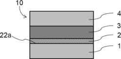
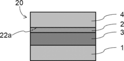
- FIG. 1 and 2 show a configuration example of the transfer film.
- the transfer film of the present invention is not limited to those having the configurations shown in FIGS. 1 and 2.
- FIG. 1 is a schematic view showing an example of the configuration of the transfer film.
- the temporary support 1, the conductive layer 2, the photosensitive resin layer 3, and the protective film 4 are laminated in this order.
- a second binder polymer and a second ethylenically unsaturated compound are present on the surface 22a of the conductive layer 2 opposite to the photosensitive resin layer 3.
- FIG. 2 is a schematic view showing another example of the structure of the transfer film.
- the temporary support 1, the photosensitive resin layer 3, the conductive layer 2, and the protective film 4 are laminated in this order. Further, a second binder polymer and a second ethylenically unsaturated compound are present on the surface 22a of the conductive layer 2 opposite to the photosensitive resin layer 3.
- the transfer film of the present invention has a temporary support.
- the temporary support include a glass substrate and a resin film, and a resin film is preferable, and a resin film having heat resistance and solvent resistance is more preferable.
- a film having flexibility and not causing significant deformation, shrinkage, or elongation under pressure, pressure, and heating is preferable.
- a resin film include polyethylene terephthalate (PET) film, polyethylene film, polypropylene film, and polycarbonate film. Of these, polyethylene terephthalate film is preferable because it is more excellent in transparency and heat resistance.
- the surface of the resin film may be release-treated so that it can be easily peeled off from the photosensitive layer later.
- 10 particles / mm 2 or more having a diameter of 5 ⁇ m or more are present on the surface opposite to the side on which the conductive layer is formed, 10 to 120. More preferably, there are 2 pieces / mm 2.
- the upper limit of the diameter of the particles is, for example, 10 ⁇ m or less.
- the thickness of the temporary support is preferably 5 ⁇ m or more, more preferably 10 ⁇ m or more, still more preferably 15 ⁇ m or more, in that the mechanical strength is more excellent.
- the thickness of the temporary support is preferably 300 ⁇ m or less, more preferably 200 ⁇ m or less, and more preferably 100 ⁇ m in that the resolution of the conductive pattern is more excellent when the photosensitive resin layer is irradiated with the active light beam through the temporary support.
- the following is more preferable. From the above points, the thickness of the temporary support is preferably 5 to 300 ⁇ m, more preferably 10 to 200 ⁇ m, and even more preferably 15 to 100 ⁇ m.
- the haze value of the temporary support is preferably 0.01 to 5.0%, more preferably 0.01 to 3.0%, and 0, in that the exposure sensitivity of the photosensitive resin layer and the resolution of the conductive pattern are more excellent. 0.01 to 2.0% is more preferable, and 0.01 to 1.5% is particularly preferable.
- the haze value is determined by a method based on JIS K 7105 (optical property test method for plastics), for example, using a commercially available turbidity meter such as NDH-1001DP (manufactured by Nippon Denshoku Industries Co., Ltd., trade name). Can be measured.
- the temporary support preferably has a light transmittance of 50% or more at the wavelength of the irradiating active light (more preferably 365 nm) in that the exposure sensitivity of the photosensitive resin layer and the resolution of the conductive pattern are more excellent. , 60% or more, more preferably 70% or more.
- the transmittance of the layer included in the transfer film is the emission light emitted through the layer with respect to the intensity of the incident light when the light is incident in the direction perpendicular to the main surface of the layer (thickness direction). It is a ratio of intensity and is measured using MCPD Series manufactured by Otsuka Electronics Co., Ltd.
- the film used as the temporary support has no deformation such as wrinkles or scratches. It is preferable that the number of fine particles, foreign substances, and defects contained in the temporary support is small in that the pattern forming property at the time of pattern exposure via the temporary support and the transparency of the temporary support are more excellent.
- the number of foreign substances and defects having a diameter of 1 ⁇ m or more is preferably 50 pieces / 10 mm 2 or less, and 10 pieces / 10 mm 2 It is more preferably 3 pieces / 10 mm 2 or less, and further preferably 3 pieces / 10 mm 2.
- the transfer film of the present invention has a conductive layer.
- the conductive layer may be arranged on the surface of the photosensitive resin layer facing the temporary support, or may be arranged on the surface of the photosensitive resin layer opposite to the surface facing the temporary support.
- the conductive layer contains at least conductive fibers containing silver nanowires. By including conductive fibers containing silver nanowires in the conductive layer, the conductivity of the layer is ensured. Further, the conductive layer contains a second binder polymer and a second ethylenically unsaturated compound. However, the second binder polymer and the second ethylenically unsaturated compound are present at least on the surface of the conductive layer opposite to the photosensitive resin layer. When the transfer film of the present invention is used to form a laminate, the second binder polymer and the second ethylenically unsaturated compound are present at least on the surface of the conductive layer opposite to the photosensitive resin layer.
- the developing solution is more likely to come into contact with the unexposed portion, and the development residue in the unexposed portion is less likely to remain.
- the silver nanowire is firmly fixed in the exposed portion by the cured resin derived from the second binder polymer and the second ethylenically unsaturated compound, the silver nanowire in the exposed portion is fixed during the developing process. Outflow to the developing solution is suppressed. As a result of suppressing the outflow of the developer of silver nanowires in the exposed portion, a laminated body having excellent conductivity can be formed.
- the second binder polymer and the second ethylenically unsaturated compound may be unevenly distributed in the conductive layer as long as they are present at least on the surface of the conductive layer opposite to the photosensitive resin layer. However, it may be dispersed over the entire layer.
- the structure of the conductive layer is not particularly limited as long as it can obtain conductivity in the plane direction, but the conductive fibers in the conductive layer are in contact with each other to form a network structure. Is preferable.
- the conductive fibers form the above-mentioned network structure in the conductive layer
- the second binder polymer and the second ethylenically unsaturated compound are the photosensitive resin layer having the network structure in which the conductive fibers are in contact with each other. Is at least present on the opposite surface.
- the identification and quantification of the second binder polymer and the second ethylenically unsaturated compound on the surface of the conductive layer opposite to the photosensitive resin layer is performed by a time-of-flight secondary ion mass spectrometer (TOF-SIMS: Time-). It can be measured using of-Flight Secondary Ion Mass Spectrometry).
- TOF-SIMS time-of-flight secondary ion mass spectrometer
- the surface of the conductive layer opposite to the photosensitive resin layer is observed with a scanning electron microscope (SEM). Then, usually, a region where an organic component such as a second binder polymer and a second ethylenically unsaturated compound is present and a region where the conductive fibers are exposed are observed.
- SEM scanning electron microscope
- the area ratio of the region where the conductive fibers are exposed on the surface of the conductive layer opposite to the photosensitive resin layer is preferably 20% or less.
- the lower limit is not particularly limited, but is, for example, 1% or more in that the developability is more excellent.
- the area ratio of the exposed regions of the conductive fibers was observed with a scanning electron microscope (SEM), and the conductive fibers were arbitrarily extracted in 16 1 mm square regions based on the obtained observation image. The value obtained by measuring the area ratio of the exposed area and calculating the average value is intended.
- the thickness of the conductive layer varies depending on the use of the conductive pattern produced by using the transfer film and the required conductivity, but is preferably 1 ⁇ m or less, more preferably 1 nm or more and 0.5 ⁇ m or less, and 5 nm or more and 0.1 ⁇ m. The following is more preferable.
- the thickness of the conductive layer is 1 ⁇ m or less, the light transmittance in the wavelength range of 450 to 650 nm is high, the pattern forming property is also excellent, and it is particularly suitable for producing a transparent electrode.
- the conductive layer is preferably arranged on the surface of the photosensitive resin layer facing the temporary support, because the effect of the present invention is more excellent. That is, the transfer film of the present invention preferably has a temporary support, a conductive layer, and a photosensitive resin layer in this order.
- the conductive fibers include silver nanowires.
- the silver nanowire is a wire-like conductive substance composed of silver or an alloy composed of silver and a metal other than silver.
- the silver nanowire may have a structure in which a wire-shaped core made of silver is coated with a metal other than silver.
- the structure coated with a metal other than silver includes not only a structure in which the entire surface of the core silver nanowire is coated, but also a structure in which a part thereof is coated.
- a metal nobler than silver is preferable, gold, platinum, or palladium is more preferable, and gold is further preferable.
- the shape of the silver nanowire is not particularly limited and may be appropriately selected depending on the intended purpose. Examples thereof include a columnar shape, a rectangular parallelepiped shape, and a columnar shape having a polygonal cross section.
- the fiber diameter of the silver nanowire is preferably 1 to 50 nm, more preferably 2 to 20 nm, and even more preferably 3 to 10 nm.
- the fiber length of the silver nanowire is preferably 1 to 100 ⁇ m, more preferably 2 to 50 ⁇ m, and even more preferably 3 to 10 ⁇ m.
- the fiber diameter and fiber length of the silver nanowires are determined by arbitrarily selecting 20 silver nanowires from an observation image containing a plurality of silver nanowires obtained by using a scanning electron microscope (SEM). It is a value obtained by arithmetically averaging the lengths of the minor axis and the major axis of silver nanowires.
- Examples of the method for producing silver nanowires include a method of reducing silver ions with a reducing agent such as NaBH 4 and a method of producing silver nanowires by a polyol method. Further, a method for producing silver nanowires is described in paragraphs 0019 to 0024 of JP2011-149902A, and the contents of this publication are incorporated in the present specification.
- the conductive layer may contain conductive fibers other than silver nanowires.
- conductive fibers other than silver nanowires include metals such as gold, silver, copper and platinum, metal fibers made of alloys of these metals, and carbon fibers such as carbon nanotubes.
- the shape of the conductive fiber may be the same as the shape of the silver nanowire described above, including its preferred embodiment.
- the conductive layer may contain an organic conductor as well as conductive fibers.
- the organic conductor is not particularly limited, and examples thereof include organic conductors such as polymers of thiophene derivatives and aniline derivatives. More specifically, polyethylene dioxythiophene, polyhexylthiophene, and polyaniline can be mentioned.
- the conductive layer contains a second binder polymer.
- the second binder polymer is not particularly limited, and for example, the same binder polymer as the first binder polymer contained in the photosensitive resin layer can be used, and the preferred embodiment is also the same.
- the first binder polymer will be described later.
- the second binder polymer may be the same binder polymer as the first binder polymer, or may be different from each other. That is, the first binder polymer and the second binder polymer may be of the same type (the same type of binder polymer).
- the second binder polymer is preferably the same binder polymer as the first binder polymer in that the effect of the present invention is more excellent. In other words, it is preferable that the binder polymer contained in the conductive layer and the binder polymer contained in the photosensitive resin layer are of the same type.
- the conductive layer contains a second ethylenically unsaturated compound.
- the second ethylenically unsaturated compound is not particularly limited, and for example, the same compound as the first ethylenically unsaturated compound contained in the photosensitive resin layer can be used, and the preferred embodiment is also the same.
- the first ethylenically unsaturated compound will be described later.
- the second ethylenically unsaturated compound may be the same ethylenically unsaturated compound as the first ethylenically unsaturated compound, or may be different from each other. That is, the first ethylenically unsaturated compound and the second ethylenically unsaturated compound may be of the same type (the same type of ethylenically unsaturated compound).
- the second ethylenically unsaturated compound is preferably the same species as the first ethylenically unsaturated compound in that the effect of the present invention is more excellent.
- the ethylenically unsaturated compound contained in the conductive layer and the ethylenically unsaturated compound contained in the photosensitive resin layer are preferably of the same type.
- Examples of the method for forming the conductive layer include the following forming methods.
- (Embodiment 1) A composition containing a second binder polymer and a second ethylenically unsaturated compound (hereinafter, also referred to as “clear layer forming composition”) is prepared, and a clear layer is formed on the surface of the temporary support. After applying the forming composition, a step of drying the coating film of the clear layer forming composition to form a clear layer and a conductive fiber-containing composition containing conductive fibers containing silver nanowires are prepared.
- a method including a step of applying a conductive fiber-containing composition to the surface of the clear layer, and then drying and pressurizing the coating film of the conductive fiber-containing composition to form a conductive layer.
- a composition for forming a conductive layer containing a second binder polymer, a second ethylenically unsaturated compound, and conductive fibers containing silver nanowires is prepared, and a temporary support or photosensitive is prepared.
- a method including a step of applying a conductive layer forming composition to the surface of a resin layer and then drying a coating film of the conductive layer forming composition to form a conductive layer.
- the method of the first embodiment is preferable in that the effect of the present invention is more excellent.
- the method of the first embodiment will be described.
- the composition for forming a clear layer only needs to contain a second binder polymer and a second ethylenically unsaturated compound.
- Materials contained in the clear layer forming composition for example, binder polymer, ethylenically unsaturated compound, photopolymerization initiator, solvent, other additives, etc. are included in the photosensitive resin layer forming composition described later. Materials can be used, and the preferred embodiments thereof are the same.
- Examples of the method for applying the clear layer forming composition include known methods such as a roll coating method, a comma coating method, a gravure coating method, an air knife coating method, a die coating method, a bar coating method, and a spray coating method. However, it is not limited to these.
- the thickness of the clear layer is not particularly limited, but is preferably 0.1 ⁇ m or less, and more preferably 0.05 ⁇ m or less. The lower limit is, for example, 1 nm or more.
- the method for drying the coating film of the clear layer forming composition is not particularly limited. For example, a method of applying hot air having a temperature of 30 to 150 ° C. to the coating film for 1 to 30 minutes using a hot air convection dryer is used. Can be mentioned.
- the content of conductive fibers in the conductive fiber-containing composition is not limited as long as the coating film of the conductive fiber-containing composition can be formed, but is 0.01 with respect to the total mass of the conductive fiber-containing composition. It is preferably from 20% by mass, more preferably 0.1 to 10% by mass.
- the conductive fiber-containing composition preferably contains a solvent.
- the solvent include water and organic solvents.
- the conductive fiber-containing composition preferably contains water as a solvent, and more preferably contains water and an organic solvent.
- an alcohol solvent is preferable.
- the alcohol-based solvent is not particularly limited, and for example, alcohol having 1 to 5 carbon atoms, ethylene glycol, polyethylene glycol, polyethylene glycol alkyl ether, glycerin, alkanediol propylene glycol having 3 to 6 carbon atoms, dipropylene glycol, 1 -Ethoxy-2-propanol, ethanolamine and diethanolamine can be mentioned.
- the water is not particularly limited, but preferably does not contain impurities.
- the conductive fiber-containing composition may contain at least one selected from the group consisting of the above-mentioned organic conductors and dispersion stabilizers such as surfactants.
- the content of water in the conductive fiber-containing composition is preferably 80% by mass or more, more preferably 90% by mass or more, based on the total mass of the conductive fiber-containing composition.
- the upper limit is not particularly limited, but is preferably 99.99% by mass or less, more preferably 99.90% by mass or less, based on the total mass of the conductive fiber-containing composition.
- the conductive fiber-containing composition contains an organic solvent, the content of the organic solvent is preferably 0.01 to 20% by mass.
- Examples of the method for applying the conductive fiber-containing composition include known methods such as a roll coating method, a comma coating method, a gravure coating method, an air knife coating method, a die coating method, a bar coating method, and a spray coating method. However, it is not limited to these.
- the thickness of the coating film of the conductive fiber-containing composition is preferably 1 nm or more and 0.5 ⁇ m or less, and more preferably 5 nm or more and 0.1 ⁇ m or less.
- the method for drying the coating film of the conductive fiber-containing composition is not particularly limited. For example, a method of applying hot air having a temperature of 30 to 150 ° C. to the coating film for 1 to 30 minutes using a hot air convection dryer is used. Can be mentioned.
- the method of pressurizing the coating film of the conductive fiber-containing composition is not particularly limited, and examples thereof include a method of pressurizing at room temperature (25 ° C.) with a linear pressure of 1 to 30 kg / cm
- the transfer film of the present invention contains a photosensitive resin layer containing a first binder polymer, a first ethylenically unsaturated compound, and a photopolymerization initiator.
- the photosensitive resin layer When the transfer film of the present invention is exposed to active light, the photosensitive resin layer usually has a reduced solubility in a developing solution in the exposed portion due to exposure, and the non-exposed portion can be removed by development.
- first binder polymer examples include (meth) acrylic resin, styrene resin, epoxy resin, amide resin, amide epoxy resin, alkyd resin, phenol resin, ester resin, urethane resin, epoxy resin and (meth) acrylic acid.
- acrylic resin examples include an epoxy acrylate resin obtained by the reaction and an acid-modified epoxy acrylate resin obtained by the reaction of the epoxy acrylate resin and the acid anhydride.
- the (meth) acrylic resin means a resin having a structural unit derived from the (meth) acrylic compound.
- the content of the structural unit derived from the (meth) acrylic compound is preferably 50% by mass or more, more preferably 70% by mass or more, still more preferably 90% by mass or more, based on all the structural units of the (meth) acrylic resin. ..
- the (meth) acrylic resin may be composed of only the structural units derived from the (meth) acrylic compound, or may have the structural units derived from the polymerizable monomer other than the (meth) acrylic compound. .. That is, the upper limit of the content of the structural unit derived from the (meth) acrylic compound is 100% by mass or less with respect to the total mass of the (meth) acrylic resin.
- Examples of the (meth) acrylic compound include (meth) acrylic acid, (meth) acrylic acid ester, (meth) acrylamide, and (meth) acrylonitrile.
- Examples of the (meth) acrylic acid ester include (meth) acrylic acid alkyl ester, (meth) acrylic acid tetrahydrofurfuryl ester, (meth) acrylic acid dimethylaminoethyl ester, (meth) acrylic acid diethylaminoethyl ester, and (meth) acrylic acid ester.
- Acrylic acid glycidyl ester (meth) acrylic acid benzyl ester, 2,2,2-trifluoroethyl (meth) acrylate, and 2,2,3,3-tetrafluoropropyl (meth) acrylate.
- Acrylic acid alkyl ester is preferable.
- (meth) acrylamide include acrylamide such as diacetone acrylamide.
- Examples of the (meth) acrylic acid alkyl ester include methyl (meth) acrylate, ethyl (meth) acrylate, propyl (meth) acrylate, butyl (meth) acrylate, pentyl (meth) acrylate, and (meth).
- (meth) acrylic acid ester a (meth) acrylic acid alkyl ester having an alkyl group having 1 to 4 carbon atoms is preferable, and methyl (meth) acrylate or ethyl (meth) acrylate is more preferable.
- the (meth) acrylic resin may have a structural unit other than the structural unit derived from the (meth) acrylic compound.
- the polymerizable monomer forming the above-mentioned structural unit is not particularly limited as long as it is a compound other than the (meth) acrylic compound that is copolymerizable with the (meth) acrylic compound, and is, for example, styrene, vinyltoluene and ⁇ -methyl.
- Styrene compounds which may have a substituent at the ⁇ -position such as styrene or an aromatic ring, vinyl alcohol esters such as acrylonitrile and vinyl-n-butyl ether, maleic acid, maleic acid anhydride, monomethyl maleate, monoethyl maleate and Examples thereof include maleic acid monoesters such as monoisopropyl maleate, fumaric acid, silicic acid, ⁇ -cyanosilicic acid, itaconic acid and crotonic acid. These polymerizable monomers may be used alone or in combination of two or more.
- the (meth) acrylic resin preferably has a structural unit having an acid group from the viewpoint of improving the alkali developability.
- the acid group include a carboxy group, a sulfo group, a phosphoric acid group and a phosphonic acid group.
- the (meth) acrylic resin more preferably has a structural unit having a carboxyl group, and further preferably has a structural unit derived from the above-mentioned (meth) acrylic acid.
- the content of the constituent unit having an acid group (preferably the constituent unit derived from (meth) acrylic acid) in the (meth) acrylic resin is excellent in developability with respect to the total mass of the (meth) acrylic resin. 10% by mass or more is preferable.
- the upper limit is not particularly limited, but is preferably 50% by mass or less, more preferably 40% by mass or less, in terms of excellent alkali resistance.
- the (meth) acrylic resin has a structural unit derived from the above-mentioned (meth) acrylic acid alkyl ester.
- the content of the structural unit derived from the (meth) acrylic acid alkyl ester in the (meth) acrylic resin is preferably 50 to 90% by mass, more preferably 65 to 90% by mass, based on all the structural units of the (meth) acrylic resin. preferable.
- the (meth) acrylic resin a resin having both a structural unit derived from (meth) acrylic acid and a structural unit derived from (meth) acrylic acid alkyl ester is preferable, and the structural unit derived from (meth) acrylic acid and the structural unit derived from (meth) acrylic acid are preferable.
- a resin composed only of structural units derived from the (meth) acrylic acid alkyl ester is more preferable.
- an acrylic resin having a structural unit derived from methacrylic acid, a structural unit derived from methyl methacrylate, and a structural unit derived from ethyl acrylate is also preferable.
- the (meth) acrylic resin is a group consisting of a structural unit derived from methacrylic acid and a structural unit derived from methacrylic acid alkyl ester in that the protective film is excellent in peelability and / or the effect of the present invention is more excellent. It is preferable to have at least one selected from the above, and it is preferable to have both a structural unit derived from methacrylic acid and a structural unit derived from an alkyl methacrylate ester.
- the total content of the structural unit derived from methacrylic acid and the structural unit derived from methacrylic acid alkyl ester in the (meth) acrylic resin is that the protective film is excellent in peelability and / or the effect of the present invention is more excellent.
- the upper limit is not particularly limited and may be 100% by mass or less, and 80% by mass or less is preferable in that the developability of the photosensitive resin layer after transfer and the laminating property of the photosensitive resin layer are more excellent.
- the (meth) acrylic resin is at least one selected from the group consisting of a structural unit derived from methacrylic acid and a structural unit derived from methacrylic acid alkyl ester in that the effect of the present invention is more excellent, and acrylic acid. It is also preferable to have at least one selected from the group consisting of the structural unit derived from the acrylic acid alkyl ester and the structural unit derived from the acrylic acid alkyl ester. In that the effect of the present invention is more excellent, the total content of the structural unit derived from methacrylic acid and the structural unit derived from methacrylic acid alkyl ester is derived from the structural unit derived from acrylic acid and the acrylic acid alkyl ester.
- the mass ratio is preferably 60/40 to 80/20 with respect to the total content of the structural units.
- the first binder polymer preferably has an ester group at the end because it is excellent in the developability of the photosensitive resin layer after transfer.
- Examples of the mode in which the first binder polymer has an ester group at the end include a mode in which the (meth) acrylic resin has an ester group at the end.
- the terminal portion of the (meth) acrylic resin is composed of a site derived from the polymerization initiator used in the synthesis.
- a (meth) acrylic resin having an ester group at the terminal can be synthesized by using a polymerization initiator that generates a radical having an ester group.
- the weight average molecular weight Mw of the first binder polymer is preferably 5,000 to 300,000, more preferably 20,000 to 150,000, in that the balance between mechanical strength, developer resistance and developability is more excellent. It is preferable, and more preferably 30,000 to 100,000.
- the photosensitive resin layer may contain only one type of the above-mentioned resin as the first binder polymer, or may contain two or more types of the above-mentioned resin.
- the two or more kinds of resins that the photosensitive resin layer may contain include, for example, two or more kinds of resins having different constituent units, two or more kinds of resins having different weight average molecular weights, and two or more kinds of resins having different dispersities. Resin can be mentioned.
- the content of the first binder polymer is preferably 10 to 90% by mass and 20 to 80% by mass with respect to the total mass of the photosensitive resin layer in that the strength of the cured film and the handleability in the transfer film are more excellent. % Is more preferable, and 30 to 70% by mass is further preferable.
- the photosensitive resin layer contains a first ethylenically unsaturated compound.
- the first ethylenically unsaturated compound is a compound having one or more ethylenically unsaturated groups in the molecule.
- As the ethylenically unsaturated group an acryloyl group or a methacryloyl group is preferable.
- the photosensitive resin layer preferably contains a bifunctional or higher functional ethylenically unsaturated compound as the first ethylenically unsaturated compound in that the curability after curing is more excellent and the effect of the present invention is more excellent. It is more preferable to contain a trifunctional or higher functional ethylenically unsaturated compound, and even more preferably to contain a trifunctional or tetrafunctional ethylenically unsaturated compound.
- a bifunctional or higher functional ethylenically unsaturated compound means a compound having two or more ethylenically unsaturated groups in the molecule, and a trifunctional or tetrafunctional ethylenically unsaturated compound is a molecule. It means a compound having 3 or 4 ethylenically unsaturated groups in it.
- Examples of the first ethylenically unsaturated compound include a compound obtained by reacting a polyhydric alcohol with an ⁇ , ⁇ -unsaturated carboxylic acid, and a glycidyl group-containing compound with an ⁇ , ⁇ -unsaturated carboxylic acid.
- a urethane monomer such as a (meth) acrylate compound having a urethane bond, ⁇ -chloro- ⁇ -hydroxypropyl- ⁇ '-(meth) acryloyloxyethyl-o-phthalate, ⁇ -hydroxyethyl- ⁇ '-( Examples thereof include phthalic acid compounds such as meta) acryloyloxyethyl-o-phthalate and ⁇ -hydroxypropyl- ⁇ '-(meth) acryloyloxyethyl-o-phthalate, and (meth) acrylic acid alkyl esters. These are used alone or in combination of two or more.
- Examples of the compound obtained by reacting a polyvalent alcohol with ⁇ , ⁇ -unsaturated carboxylic acid include 2,2-bis (4-((meth) acryloxypolyethoxy) phenyl) propane and 2,2-bis.
- Bisphenol A-based (meth) acrylate compounds such as (4-((meth) acryloxypolypropoxy) phenyl) propane and 2,2-bis (4-((meth) acryloxypolyethoxypolypropoxy) phenyl) propane, Polyethylene glycol di (meth) acrylate having 2 to 14 ethylene oxide groups, polypropylene glycol di (meth) acrylate having 2 to 14 propylene oxide groups, and 2 to 14 ethylene oxide groups.
- an ethylene unsaturated compound having a tetramethylolmethane structure or a trimethylolpropane structure is preferable, and tetramethylolmethanetri (meth) acrylate, tetramethylolmethanetetra (meth) acrylate, trimethylolpropane tri (meth) acrylate or di ( Trimethylolpropane) tetraacrylate is more preferred.
- the urethane monomer examples include a (meth) acrylic monomer having a hydroxyl group at the ⁇ -position and a diisocyanate compound such as isophorone diisocyanate, 2,6-toluene diisocyanate, 2,4-toluene diisocyanate, and 1,6-hexamethylene diisocyanate.
- a diisocyanate compound such as isophorone diisocyanate, 2,6-toluene diisocyanate, 2,4-toluene diisocyanate, and 1,6-hexamethylene diisocyanate.
- Tris [(meth) acryloxytetraethylene glycol isocyanate] hexamethylene isocyanurate, ethylene oxide-modified urethane di (meth) acrylate, and ethylene oxide and propylene oxide-modified urethane di (meth) acrylate examples include Tris [(meth) acryloxytetraethylene glycol is
- Examples of the ethylene oxide-modified urethane di (meth) acrylate include "UA-11” (manufactured by Shin-Nakamura Chemical Industry Co., Ltd., trade name). Examples of ethylene oxide and propylene oxide-modified urethane di (meth) acrylate include “UA-13” (manufactured by Shin-Nakamura Chemical Industry Co., Ltd., trade name).
- an ethylenically unsaturated compound containing an ester bond is preferable in terms of further improving developability.
- the ethylenically unsaturated compound containing an ester bond is not particularly limited as long as it contains an ester bond in the molecule, but an ethylene unsaturated compound having a tetramethylolmethane structure or a trimethylolpropane structure is excellent in that the effect of the present invention is excellent.
- the ethylenically unsaturated compound includes an ethylenically unsaturated compound having an aliphatic group having 6 to 20 carbon atoms and the above-mentioned ethylene unsaturated compound having a tetramethylol methane structure or a trimethylol propane structure. It preferably contains a compound.
- Examples of the ethylenically unsaturated compound having an aliphatic structure having 6 or more carbon atoms include 1,9-nonanediol di (meth) acrylate, 1,10-decanediol di (meth) acrylate, and tricyclodecanedimethanol di (meth) acrylate. Meta) acrylate can be mentioned. From the viewpoint of imparting flexibility, an ethylenically unsaturated compound having a linear aliphatic group having 6 to 20 carbon atoms or the above-mentioned urethane monomer and the above-mentioned ethylene unsaturated compound having a tetramethylolmethane structure or a trimethylolpropane structure.
- Examples of the ethylenically unsaturated compound having a linear aliphatic group having 6 to 20 carbon atoms include 1,9-nonanediol di (meth) acrylate and 1,10-decanediol di (meth) acrylate.
- the photosensitive resin layer may contain only one type of the first ethylenically unsaturated compound, or may contain two or more types.
- the content of the first ethylenically unsaturated compound is preferably 30 to 80 parts by mass, preferably 30 to 70 parts by mass, based on 100 parts by mass of the total amount of the first binder polymer and the first ethylenically unsaturated compound. More preferred. 30 parts by mass or more is preferable from the viewpoint of excellent photocurability and coatability on the formed conductive layer, and 80 parts by mass or less is preferable from the viewpoint of excellent storage stability when wound as a film.
- the content of the first ethylenically unsaturated compound in the photosensitive resin layer is preferably 1 to 70% by mass, more preferably 10 to 60% by mass, and 20 to 50% by mass, based on the total mass of the photosensitive resin layer. Mass% is more preferred.
- the molecular weight of the first ethylenically unsaturated compound is preferably 200 to 3,000, more preferably 250 to 2,600, and 280 to 2,200. Is more preferable, and 300 to 2,200 is particularly preferable.
- the photosensitive resin layer contains a photopolymerization initiator.
- the photopolymerization initiator is particularly any compound capable of polymerizing the first ethylenically unsaturated compound by irradiation with active light such as ultraviolet rays, visible light, and X-rays to cure the photosensitive resin layer. Not limited.
- Examples of the photopolymerization initiator include a photoradical polymerization initiator and a photocationic polymerization initiator, and a photoradical polymerization initiator is preferable because it has more excellent photocurability.
- Examples of the photoradical polymerization initiator include a photopolymerization initiator having an oxime ester structure (hereinafter, also referred to as “oxym ester compound”), a photopolymerization initiator having an ⁇ -aminoalkylphenone structure, and an ⁇ -hydroxyalkylphenone structure.
- Examples thereof include a photopolymerization initiator having an acylphosphine oxide structure, a photopolymerization initiator having an acylphosphine oxide structure (hereinafter, also referred to as “acylphosphine oxide-based compound”), and a photopolymerization initiator having an N-phenylglycine structure.
- More specific photoradical polymerization initiators include, for example, benzophenone, N, N'-tetramethyl-4,4'-diaminobenzophenone (Michlerketone), N, N'-tetraethyl-4,4'-diaminobenzophenone, and the like.
- Aclysin derivatives such as: N-phenylglycine, N-phenylglycine derivatives, coumarin compounds, oxazole compounds; 2,4,6-trimethylbenzoyl-diphenyl-phosphine oxide, and bis (2,4,6-trimethylbenzoyl).
- -Acylphosphine oxide-based compounds such as phenylphosphine oxide can be mentioned.
- the substituents of the two aryl groups in 2,4,5-triarylimidazole may be the same or different.
- a thioxanthone-based compound and a tertiary amine compound may be combined, such as a combination of diethylthioxanthone and dimethylaminobenzoic acid.
- the photoradical polymerization initiator for example, the photopolymerization initiator described in paragraphs 0031 to 0042 of JP2011-0957116 and paragraphs 0064 to 0081 of JP2015-014783 may be used.
- oxime ester compounds or acylphosphine oxide compounds are preferable because they are more excellent in transparency and pattern forming ability at 10 ⁇ m or less, and 2-benzyl-2-dimethylamino-1- (4-morpholinophenyl) is preferable.
- 2-benzyl-2-dimethylamino-1- (4-morpholinophenyl) is preferable.
- the content of the photopolymerization initiator is preferably 0.05 to 0.5 by mass ratio with respect to the content of the compound having the first ethylenically unsaturated group, and is 0.1 to 0.5. Is more preferable.
- the photosensitive resin layer may contain only one type of photopolymerization initiator, or may contain two or more types of photopolymerization initiators.
- the content of the photopolymerization initiator is not particularly limited, but is preferably 0.1 to 20% by mass, more preferably 0.5 to 15% by mass, and 1 to 10% by mass with respect to the total mass of the photosensitive resin layer. % Is more preferable.
- the content of the photopolymerization initiator is preferably 0.1 to 20 parts by mass, preferably 1 to 15 parts by mass, based on 100 parts by mass of the total amount of the first binder polymer and the first ethylenically unsaturated compound. More preferably, 1 to 12 parts by mass is further preferable. From the viewpoint of excellent light sensitivity, 0.1 part by mass or more is preferable, and from the viewpoint of excellent photocurability inside the photosensitive resin layer, 20 parts by mass or less is preferable.
- the photosensitive resin layer preferably contains a leveling agent in that the composition for forming the photosensitive resin layer is more excellent in coatability.
- the leveling agent include various surfactants such as silicone-based surfactants, fluorine-based surfactants, nonionic surfactants, cationic surfactants, and anionic surfactants, and silicone-based surfactants. Is preferable.
- the silicone-based surfactant include a linear polymer composed of a siloxane bond and a modified siloxane polymer having an organic group introduced into a side chain or a terminal.
- Specific examples of the leveling agent include Toray Dow Corning Co., Ltd., DOWNSIL8032 ADDITIVE, and Shin-Etsu Chemical Co., Ltd.
- first binder polymer and the silicone-based surfactant in combination from the viewpoint of achieving both the coatability of the composition for forming the photosensitive resin layer and the developability of the photosensitive resin layer after transfer.
- the photosensitive resin layer preferably contains a phosphoric acid ester compound in terms of further improving the adhesion of the photosensitive resin layer to the substrate or the conductive layer.
- the photosensitive resin layer may contain only one type of phosphoric acid ester compound, or may contain two or more types.
- the content of the phosphoric acid ester compound is not particularly limited, but is preferably 0.05 to 3.0% by mass, more preferably 0.1 to 2.0% by mass, based on the total mass of the photosensitive resin layer. 0.2 to 1.0% by mass is more preferable.
- the content of the phosphoric acid ester compound is not particularly limited, but the binder polymer and ethylene are not used in terms of further improving the adhesion of the photosensitive resin layer to the substrate or the conductive layer. It is preferably 10 parts by mass or less, more preferably 3 parts by mass or less, based on 100 parts by mass of the total saturated compound. Further, it is preferably 0.01 part by mass or more, and more preferably 0.1 part by mass or more.
- the photosensitive resin layer may contain various additives, if necessary.
- Additives include plasticizers such as p-toluenesulfonamide, fillers, defoamers, flame retardants, stabilizers, adhesion imparting agents, peeling accelerators, antioxidants, fragrances, imaging agents, and thermal cross-linking agents. And so on.
- the photosensitive resin layer may contain a photosensitive additive alone or in combination of two or more.
- the amount of these additives added is preferably 0.01 to 20 parts by mass with respect to 100 parts by mass of the total amount of the first binder polymer and the first ethylene unsaturated compound.
- the thickness of the photosensitive resin layer is not particularly limited, but the thickness after drying is preferably 1 to 200 ⁇ m, more preferably 2 to 15 ⁇ m, still more preferably 3 to 10 ⁇ m.
- the thickness of the photosensitive resin layer is 1 ⁇ m or more, the layer formation by coating the composition for forming the photosensitive resin layer tends to be easy. Further, when the thickness of the photosensitive resin layer is 200 ⁇ m or less, the light transmittance and the sensitivity are improved, and the photocurability of the photosensitive resin layer is more excellent, which is preferable.
- a silicon atom is present on the surface of the photosensitive resin layer opposite to the conductive layer.
- the identification and quantification of silicon atoms on the surface of the photosensitive resin layer opposite to the conductive layer can be measured using a time-of-flight secondary ion mass spectrometer (TOF-SIMS).
- TOF-SIMS time-of-flight secondary ion mass spectrometer
- the photosensitive resin layer contains a silicone-based surfactant (for example, a linear polymer composed of a siloxane bond and a modified siloxane polymer having an organic group introduced into a side chain or a terminal) as a leveling agent
- Silicon atoms are often present on the surface of the photosensitive resin layer opposite to the conductive layer.
- the method for forming the photosensitive resin layer is not particularly limited as long as it is a method capable of forming a layer containing the above components.
- a method for forming the photosensitive resin layer for example, a composition for forming a photosensitive resin layer containing a first binder polymer, a first ethylenically unsaturated compound, a photopolymerization initiator, and a solvent is prepared and temporarily supported. Examples thereof include a method in which a photosensitive resin layer forming composition is applied to the surface of a body or a conductive layer, and then the coating film of the photosensitive resin layer forming composition is dried to form a photosensitive resin layer.
- the composition for forming a photosensitive resin layer preferably contains a solvent in order to adjust the viscosity of the composition for forming a photosensitive resin layer and facilitate the formation of a coating film.
- a solvent contained in the composition for forming the photosensitive resin layer, the first binder polymer, the first ethylenically unsaturated compound, the photopolymerization initiator, and the above-mentioned additives optionally contained can be dissolved or dispersed.
- the solvent is not particularly limited, for example, methanol, ethanol, acetone, methyl ethyl ketone, methyl cellosolve, ethyl cellosolve, N, N-dimethylformamide, propylene glycol monomethyl ether, toluene, acetic acid-n-propyl, and a mixed solvent thereof can be used. Can be mentioned.
- methyl ethyl ketone, propylene glycol monomethyl ether, and a mixture thereof are particularly preferable because they are more excellent in the effects of the present invention.
- the content of the organic solvent in the photosensitive resin layer after drying prevents the organic solvent from diffusing in a later step. Therefore, it is preferably 2% by mass or less with respect to the total mass of the photosensitive resin layer.
- the content of the solvent contained in the composition for forming the photosensitive resin layer is 30 to 95% by mass with respect to the total mass of the composition for forming the photosensitive resin layer in that the developability of the photosensitive resin layer is more excellent. Is preferable, 40 to 90% by mass is more preferable, and 40 to 80% by mass is further preferable.
- a method for applying the composition for forming a photosensitive resin layer known methods such as a roll coating method, a comma coating method, a gravure coating method, an air knife coating method, a die coating method, a bar coating method, and a spray coating method are available. These are, but are not limited to.
- the method for drying the coating film of the composition for forming the photosensitive resin layer is not particularly limited, and for example, hot air having a temperature of 70 to 150 ° C. is applied to the coating film for 5 to 30 minutes using a hot air convection dryer. The method can be mentioned.
- the minimum light transmittance is preferably 80% or more, and more preferably 85% or more.
- the first binder polymer and the second binder polymer are of the same type, and the compound having the first ethylenically unsaturated group and the second ethylenically unsaturated group. It is preferable that the compound having a saturated group is the same species.
- the transfer film of the present invention is a transfer film having a temporary support, a photosensitive resin layer, and a conductive layer arranged adjacent to the photosensitive resin layer, and the photosensitive resin layer is a binder.
- the above binder polymer and the above ethylenically unsaturated group are contained on the surface of the conductive layer opposite to the photosensitive resin layer, which contains an ethylenically unsaturated compound of the same type as the compound and a conductive fiber containing silver nanowires. It is preferably a transfer film in which a compound having the above is present.
- the preferred embodiments of the binder polymer and the ethylenically unsaturated compound contained in the photosensitive resin layer and the conductive layer are the preferred embodiments of the first binder polymer and the preferred ethylenically unsaturated compound described above. Examples thereof include compounds exemplified.
- the transfer film preferably has a protective film that is in contact with a surface that does not face the temporary support.
- a resin film having heat resistance and solvent resistance can be used, and examples thereof include a polyolefin film such as a polyethylene terephthalate film, a polypropylene film, and a polyethylene film.
- a resin film made of the same material as the above-mentioned support film may be used. Among them, a polyolefin film is preferable, a polypropylene film or a polyethylene film is more preferable, and a polyethylene film is further preferable.
- the thickness of the protective film is preferably 1 to 100 ⁇ m, more preferably 5 to 50 ⁇ m, further preferably 5 to 40 ⁇ m, and particularly preferably 15 to 30 ⁇ m.
- the thickness of the protective film is preferably 1 ⁇ m or more in terms of excellent mechanical strength, and preferably 100 ⁇ m or less in terms of relatively low cost.
- the adhesive force between the protective film and the photosensitive resin layer or the conductive layer facilitates the peeling of the protective film from the photosensitive resin layer or the conductive layer, so that the temporary support and the photosensitive resin layer or the conductive layer are separated from each other. It is preferably smaller than the adhesive force.
- the protective film preferably contains 5 fish eyes / m 2 or less having a diameter of 80 ⁇ m or more.
- fisheye means that when a film is produced by heat-melting a material, kneading, extruding, biaxial stretching, casting method, etc., foreign substances, undissolved substances, oxidative deterioration substances, etc. of the material are contained in the film. It was taken in.
- the number of diameter 3 ⁇ m or more of the particles contained in the protective film is preferably at 30 / mm 2 or less, more preferably 10 or / mm 2 or less, that is five / mm 2 or less further preferable.
- the protective film preferably has an arithmetic average roughness Ra of 0.01 ⁇ m or more, preferably 0.02 ⁇ m, on the surface opposite to the surface in contact with the photosensitive resin layer or the conductive layer. It is more preferably 0.03 ⁇ m or more, and further preferably 0.03 ⁇ m or more.
- the upper limit value is preferably less than 0.50 ⁇ m, more preferably 0.40 ⁇ m or less, and further preferably 0.30 ⁇ m or less.
- the protective film preferably has an arithmetic average roughness Ra of the surface in contact with the photosensitive resin layer or the conductive layer of 0.01 ⁇ m or more, more preferably 0.02 ⁇ m or more. It is preferably 0.03 ⁇ m or more, and more preferably 0.03 ⁇ m or more.
- the upper limit value is preferably less than 0.50 ⁇ m, more preferably 0.40 ⁇ m or less, and further preferably 0.30 ⁇ m or less.
- the transfer film may further have at least one layer selected from the group consisting of an adhesive layer and a gas barrier layer on the surface of the protective film.
- the method for producing the transfer film of the present invention is not particularly limited. Hereinafter, an example of a method for producing a transfer film will be described with reference to FIGS. 1 and 2.
- the transfer film having the temporary support 1, the conductive layer 2, and the photosensitive resin layer 3 in this order is, for example, the method of the above-described embodiment 1 on the surface of the temporary support 1.
- the step of forming the conductive layer 2 and the surface of the conductive layer 2 are coated with the composition for forming the photosensitive resin layer, and then the coating film of the composition for forming the photosensitive resin layer is dried to form the photosensitive resin layer. It is manufactured by a method including the step of forming 3.
- the transfer film 10 shown in FIG. 1 is manufactured by adhering a resin film to the surface of the photosensitive resin layer 3 of the laminate manufactured by the above manufacturing method to form the protective film 4.
- the transfer film having the temporary support 1, the photosensitive resin layer 3 and the conductive layer 2 in this order has, for example, a photosensitive resin layer formed on the surface of the temporary support 1.
- the coating film of the composition for forming a photosensitive resin layer is dried to form the photosensitive resin layer 3, and the method of the above-described second embodiment, for example, on the surface of the photosensitive resin layer 3. It is manufactured by a method including a step of forming the conductive layer 2 by the above method.
- the transfer film 20 shown in FIG. 2 is manufactured by laminating a resin film on the surface of the conductive layer 2 of the laminate manufactured by the above manufacturing method to form the protective film 4.
- the order of the conductive layer and the photosensitive resin layer in the transfer film is not particularly limited, and the temporary support 1, the conductive layer 2, and the photosensitive resin layer 3 are provided in this order as in the transfer film 10 shown in FIG.
- the temporary support 1, the photosensitive resin layer 3, and the conductive layer 2 may be provided in this order as in the transfer film 20 shown in FIG.
- the conductive layer 2 and the photosensitive resin layer 3 are arranged adjacent to each other. Further, a second binder polymer and a second ethylenically unsaturated compound are present on the surface 22a of the conductive layer 2 opposite to the photosensitive resin layer 3.
- a transfer film having a temporary support, a conductive layer, and a photosensitive resin layer in this order is preferable because the effect of the present invention is more excellent.
- the laminateability is also excellent. This is because the photosensitive resin layer has higher flexibility than the conductive layer, so that bubbles or floating between the substrate and the photosensitive resin layer are suppressed during transfer.
- the transfer film may be stored, for example, in the form of a flat plate as it is, or in the form of a roll, which is wound up using a cylindrical core.
- the transfer film is wound in a roll form, it is preferable to wind the transfer film so that the temporary support is on the outermost side.
- the transfer film does not have a protective film, the transfer film can be stored as it is in a flat plate form.
- the winding core is not particularly limited as long as it is conventionally used.
- the material constituting the winding core include plastics such as polyethylene resin, polypropylene resin, polystyrene resin, polyvinyl chloride resin, and ABS resin (acrylonitrile-butadiene-styrene copolymer). It is preferable to install an end face separator on the end face of the transfer film wound in a roll shape from the viewpoint of protecting the end face, and more preferably to install a moisture-proof end face separator from the viewpoint of better edge fusion resistance. Further, when packing the transfer film, it is preferable to wrap it in a black sheet having excellent moisture permeability.
- the use of the transfer film described above is not particularly limited, but since the photosensitive resin layer after transfer is excellent in developability, a laminate having a conductive pattern obtained by patterning a conductive layer containing conductive fibers containing silver nanowires. It is preferably used as a transfer film for the body, and more preferably used as a transfer film for a touch panel.
- the above-mentioned transfer film and the substrate are bonded to each other by bringing the substrate into contact with the surface opposite to the surface on which the temporary support of the transfer film is arranged (hereinafter, "transfer”).
- a step of pattern-exposing the photosensitive resin layer of the transfer film hereinafter also referred to as “exposure step”
- exposure step a step of pattern-exposing the photosensitive resin layer of the transfer film
- development step a step of forming a patterned conductive layer (conductive pattern)
- a laminate having a substrate, a cured resin layer (cured film) obtained by curing a patterned photosensitive resin layer, and a patterned conductive layer is produced.
- the substrate contained in the laminate is not particularly limited, and examples thereof include a glass substrate and a plastic substrate such as polycarbonate.
- the thickness of the substrate can be appropriately selected according to the purpose of use.
- the substrate may be in the form of a film.
- the film-like substrate include a polyethylene terephthalate film, a polycarbonate film, and a cycloolefin polymer film.
- the substrate preferably has a minimum light transmittance of 80% or more in the wavelength range of 450 to 650 nm. When the substrate satisfies such a condition, it becomes easy to increase the brightness in the display panel or the like.
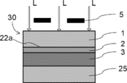
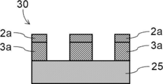
- FIGS. 3A, 3B, and 3C are schematic views for explaining an example of a method for producing a laminate using a transfer film.
- the manufacturing method using the transfer film 10 shown in FIG. 1 is described, but the manufacturing method of the laminate is not limited to the method using the transfer film having the configuration shown in FIG.
- the transfer step it is preferable to press the photosensitive resin layer side of the transfer film onto the substrate while heating the photosensitive resin layer and / or the substrate.
- the heating temperature and crimping pressure at this time are not particularly limited, but the heating temperature is preferably 70 to 130 ° C., and the crimping pressure is preferably about 0.1 to 1.0 MPa (about 1 to 10 kgf / cm 2 ). Further, it is preferable to carry out the operation under reduced pressure because the adhesion and the followability are more excellent. Further, instead of the heat treatment of the photosensitive resin layer and / or the substrate in the transfer step, the substrate may be preheat-treated before the transfer step in order to further improve the adhesion.
- the photosensitive resin layer 3 is pattern-exposed.
- a part of the photosensitive resin layer 3 is exposed by irradiating the active light L in an image shape through a mask pattern 5 called artwork.
- the photosensitive resin layer 3 is cured to form a cured film 3a.
- the photosensitive resin layer 3 is not cured in the region (unexposed portion) not irradiated with the active light L.
- Examples of the light source of the active light beam in the exposure step include a known light source.
- the light source is not particularly limited as long as it is a light source that effectively irradiates the photosensitive resin layer with light having a wavelength that can be exposed (for example, 365 nm or 405 nm).
- an Ar ion laser or a semiconductor laser may be used, or a photographic flood bulb or a solar lamp may be used.
- a method of irradiating an active ray in an image shape without using the mask pattern 5 may be adopted by a direct drawing method using a laser exposure method or the like.
- Exposure at the exposure step may vary depending on the composition of the device and the photosensitive resin layer to be used is preferably 5 ⁇ 1000mJ / cm 2, more preferably 10 ⁇ 700mJ / cm 2. From the viewpoint of excellent photocurability, 10 mJ / cm 2 or more is preferable, and from the viewpoint of resolution, 1000 mJ / cm 2 or less is preferable.
- the exposure atmosphere in the exposure process is not particularly limited, and can be performed in air, nitrogen, or vacuum.
- a peeling step of peeling the temporary support 1 from the laminated body 30 is performed after the exposure step and before the developing step.
- the method of peeling is not particularly limited, and a known method can be appropriately adopted.
- the peeling step is performed after the exposure step of pattern-exposing the photosensitive resin layer 3 via the temporary support 1, but before the exposure step.
- the peeling step of peeling the temporary support 1 from the laminated body 30 may be performed.
- a patterned conductive layer (conductive pattern 2a) is formed by removing a part of the conductive layer 2 together with the unexposed portion of the photosensitive resin layer 3. Specifically, the uncured portion (unexposed portion) of the photosensitive resin layer 3 is removed by bringing the developing solution into contact with the exposed surface of the laminated body 30 exposed by peeling the temporary support 1. At this time, not only the unexposed portion of the photosensitive resin 3 but also the region of the conductive layer 2 in contact with the unexposed portion is removed.
- a conductive pattern 2a composed of the patterned conductive layer 2 is formed, and the substrate 25, the conductive pattern 2a, and the cured film (cured resin pattern 3a) of the patterned photosensitive resin layer 3 are laminated.
- Manufacture body 30 is
- Examples of the developing solution include an alkaline aqueous solution, an aqueous developing solution, and an organic solvent-based developing solution.
- the developing process in the developing step is performed by a known method such as spraying, rocking dipping, brushing and scraping using these developers, for example.
- an alkaline aqueous solution is preferable because it is safe, stable, and has good operability.
- As the alkaline aqueous solution 0.1 to 5% by mass sodium carbonate aqueous solution, 0.1 to 5% by mass potassium carbonate aqueous solution, 0.1 to 5% by mass sodium hydroxide aqueous solution, or 0.1 to 5% by mass tetraborax.
- Aqueous sodium solution is preferred.
- the pH of the alkaline aqueous solution used as the developing solution is preferably in the range of 9 to 11.
- the temperature of the developing solution is adjusted according to the developability of the photosensitive resin layer.
- the alkaline aqueous solution may contain a surfactant, a defoaming agent, a small amount of an organic solvent for accelerating development, and the like.
- an aqueous developing solution composed of water or an alkaline aqueous solution and one or more kinds of organic solvents
- the base contained in the alkaline aqueous solution in addition to the above-mentioned sodium carbonate, potassium carbonate, sodium hydroxide and sodium tetraborate, for example, borax, sodium metasilicate, tetramethylammonium hydroxide, ethanolamine, etc.
- borax sodium metasilicate
- tetramethylammonium hydroxide ethanolamine
- examples thereof include ethylenediamine, diethylenetriamine, 2-amino-2-hydroxymethyl-1,3-propanediol, 1,3-diaminopropanol-2, and morpholin.
- organic solvent examples include methyl ethyl ketone, acetone, ethyl acetate, alkoxy ethanol having an alkoxy group having 1 to 4 carbon atoms, ethyl alcohol, isopropyl alcohol, butyl alcohol, diethylene glycol monomethyl ether, diethylene glycol monoethyl ether, and diethylene glycol monobutyl ether. Can be mentioned. These are used alone or in combination of two or more.
- the content of the organic solvent in the aqueous developer is preferably 2 to 90% by mass with respect to the total mass of the aqueous developer.
- the temperature of the aqueous developer is adjusted according to the developability of the photosensitive resin layer.
- the pH of the aqueous developer is not particularly limited as long as the photosensitive resin layer can be developed, but 8 to 12 is more preferable, and 9 to 10 is further preferable.
- the aqueous developer may contain a small amount of additives such as a surfactant and an antifoaming agent.
- organic solvent-based developer examples include 1,1,1-trichloroethane, N-methylpyrrolidone, N, N-dimethylformamide, cyclohexanone, methyl isobutyl ketone, and ⁇ -butyrolactone.
- the organic solvent-based developer preferably contains water in the range of 1 to 20% by mass in order to prevent ignition.
- the above-mentioned developer may be used in combination of two or more, if necessary.
- Examples of the development method include a dip method, a battle method, a spray method, brushing, and slapping. Of these, it is preferable to use the high-pressure spray method because the resolution is further improved.
- the conductive pattern 2a is formed by heating at 60 to 250 ° C. or exposing with an exposure amount of 0.2 to 10 J / cm 2 as necessary after the developing step. It may be further cured.
- the laminate having the conductive pattern obtained by the above manufacturing method can be applied to various uses.
- Applications of the laminate having a conductive pattern include, for example, a touch panel (touch panel sensor), a semiconductor chip, various electric wiring boards, FPC (Flexible printed circuits), COF (Chip on Film), TAB (Tape Automated Bonding), an antenna, and the like. Examples thereof include a multilayer wiring board and a motherboard, which are preferably used for a touch panel sensor.
- the conductive pattern of the laminated body functions as a detection electrode or a lead-out wiring in the touch panel sensor.
- the touch panel is not particularly limited as long as it has the above-mentioned touch panel sensor.
- the above-mentioned touch panel sensor is combined with various display devices (for example, a liquid crystal display device and an organic EL (electro-luminescence) display device).
- display devices for example, a liquid crystal display device and an organic EL (electro-luminescence) display device.
- Equipment is mentioned.
- Examples of the detection method in the touch panel sensor and the touch panel include known methods such as a resistive film method, a capacitance method, an ultrasonic method, an electromagnetic induction method, and an optical method. Of these, a capacitive touch panel sensor and a touch panel are preferable.
- the touch panel type includes a so-called in-cell type (for example, those shown in FIGS. 5, 6, 7, and 8 of Japanese Patent Application Laid-Open No. 2012-517501), and a so-called on-cell type (for example, Japanese Patent Application Laid-Open No. 2013-168125).
- the ones shown in FIG. 19 and those shown in FIGS. 1 and 5 of JP2012-081020A eg, Japanese Patent Application Laid-Open No. 2012
- OGS One Glass Solution
- TOR Touch-on-Lens
- GG various out-cell types
- G1 / G2, GFF various out-cell types
- GF various out-cell types
- other configurations for example, Japanese Patent Application Laid-Open No. 2013-164871.
- Examples of the touch panel include those described in paragraph 0229 of JP2017-120345A.
- the touch panel manufacturing method is not particularly limited, and a known touch panel manufacturing method may be referred to except that the touch panel sensor having the above-mentioned laminated body is used.
- solution 2 (a solution in which 5 g of AgNO 3 was dissolved in 300 mL of ethylene glycol) and solution 3 (a solution in which 5 g of polyvinylpyrrolidone (“PVPK30” manufactured by Nippon Catalyst Co., Ltd.) was dissolved in 150 mL of ethylene glycol) were mixed.
- PVPK30 polyvinylpyrrolidone
- 150 mL of ethylene glycol ethylene glycol
- the reaction solution was allowed to stand at 30 ° C. or lower, and then diluted 10-fold with acetone.
- the diluted solution of the above reaction solution was centrifuged at 2000 rpm for 20 minutes with a centrifuge, and the supernatant was decanted.
- Acetone was added to the precipitate, and after stirring, centrifugation was performed under the same conditions as above, and acetone was decanted. Then, it was centrifuged twice in the same manner using distilled water to obtain silver nanowires.
- the silver nanowires obtained above are dispersed in pure water so as to have a concentration of 0.2% by mass, and dodecyl-pentaethylene glycol is dispersed so as to have a concentration of 0.1% by mass.
- a dispersion liquid (silver nanowire-containing coating liquid) was obtained.
- Table 1 shows the composition of the monomer mixture containing the polymerizable monomer used for the synthesis of the polymer.
- the polymerizable monomers used in each monomer mixture are as follows. ⁇ Methacrylic acid (manufactured by Fujifilm Wako Pure Chemical Industries, Ltd.) ⁇ Methyl methacrylate (manufactured by Fujifilm Wako Pure Chemical Industries, Ltd.) ⁇ Ethyl acrylate (manufactured by Fujifilm Wako Pure Chemical Industries, Ltd.)
- the polymer A2 was synthesized by the same method as the synthesis of the polymer A1 except that the mixed solution 1 was replaced with the mixed solution 2.
- the weight average molecular weight of the obtained polymer A2 was 6,5000.
- the polymer A3 was synthesized by the same method as the synthesis of the polymer A1 except that the mixed solution 1 was replaced with the mixed solution 3.
- the weight average molecular weight of the obtained polymer A3 was 6,5000.
- Example 1 [Adjustment of composition for forming clear layer] 63 parts by mass of polymer A1 as a binder polymer in terms of solid content, and 37 parts by mass of ditrimethylolpropane tetraacrylate (corresponding to "DTPTA” in the table. "KAYARAD T-1420” manufactured by Nippon Kayaku Co., Ltd.) as an ethylenically unsaturated compound. 10 parts by mass of 2,4,6-trimethylbenzoyl-diphenyl-phosphine oxide (corresponding to "Omnirad TPO H” in the table. "Omnirad TPO H” manufactured by IGM Resins BV) as a photopolymerization initiator.
- DTPTA ditrimethylolpropane tetraacrylate
- composition for forming negative photosensitive resin layer 63 parts by mass of polymer A1 as a binder polymer in terms of solid content, and 37 parts by mass of ditrimethylolpropane tetraacrylate (corresponding to "DTPTA” in the table; "KAYARAD T-1420” manufactured by Nippon Kayaku Co., Ltd.) as an ethylenically unsaturated compound 10 parts by mass of 2,4,6-trimethylbenzoyl-diphenyl-phosphine oxide (corresponding to "Omnirad TPO H" in the table. "Omnirad TPO H” manufactured by IGM Resins BV) as a photopolymerization initiator.
- a PET film having a thickness of 16 ⁇ m and having a layer having 10 particles / mm 2 or more having a diameter of 5 ⁇ m or more on one surface was prepared.
- the prepared clear layer forming composition was uniformly applied onto the surface of the temporary support on the side opposite to the surface on which 10 particles / mm 2 or more having a diameter of 5 ⁇ m or more were present.
- the obtained coating film was dried with hot air at 100 ° C. using a hot air convection dryer for 2 minutes to form a clear layer. At this time, the film thickness of the clear layer after drying was 10 nm.
- the silver nanowire-containing coating liquid obtained above was uniformly applied to the surface of the clear layer obtained above so as to be 25 g / m 2, and the obtained coating film was applied to a hot air convection dryer. It was dried for 2 minutes by hot air at 100 ° C. After drying, the mixture was pressurized at room temperature (25 ° C.) with a linear pressure of 10 kg / cm. As a result, a conductive layer containing silver nanowires, a binder polymer, and an ethylenically unsaturated compound was formed on the temporary support. Finally, the composition for forming a negative photosensitive resin layer obtained above was stirred and then uniformly applied onto a 16 ⁇ m-thick PET film on which the conductive layer was formed. The obtained coating film was dried with hot air at 100 ° C. using a hot air convection dryer for 2 minutes to form a photosensitive resin layer.
- the total thickness of the layers formed on the temporary support by the above step was about 5 ⁇ m.
- a polyethylene protective film (manufactured by Tamapoli Co., Ltd., trade name "NF-13") was attached to the surface of the outermost photosensitive resin layer to form a protective film, and a transfer film was obtained.
- the transfer film of Example 1 contained silver nanowires, a binder polymer, and an ethylene unsaturated compound in the conductive layer.
- a laminate is produced by laminating the transfer film of Example 1 from which the protective film has been peeled off and a transparent film substrate (cycloolefin polymer film, thickness: 38 ⁇ m, refractive index: 1.53) (transfer step). did.
- the transfer step was carried out using a vacuum laminator manufactured by MCK Co., Ltd. under the conditions of substrate temperature: 40 ° C., rubber roller temperature: 100 ° C., linear pressure: 3 N / cm, and transfer speed: 2 m / min.
- the surface of the photosensitive resin layer exposed by peeling the protective film from the transfer film was brought into contact with the surface of the transparent film substrate.
- the surface of the conductive layer of the transfer film opposite to the photosensitive layer resin layer was exposed.
- the surface exposed by the above procedure was surface-analyzed by TOF-SIMS (apparatus: "SIMS5" manufactured by IONTOF), the presence or absence of an ethylenically unsaturated compound and a binder polymer was measured, and evaluated according to the following criteria.
- the presence or absence of fragment ions derived from each binder polymer for example, the presence or absence of fragment ions derived from acryloyl groups
- the presence or absence of fragment ions derived from each ethylenically unsaturated compound for example, the presence or absence of acryloyl groups.
- the presence or absence of the binder polymer and the ethylenically unsaturated compound was confirmed by the presence or absence of fragment ions derived from.
- the transfer step the surface of the photosensitive resin layer exposed by peeling the protective film from the transfer film was brought into contact with the surface of the transparent film substrate.
- the surface of the conductive layer opposite to the photosensitive layer resin layer was exposed.
- the surface exposed by the above procedure was observed with a scanning electron microscope (SEM), and the area ratio of the exposed silver nanowire region was determined in 16 1 mm square regions arbitrarily extracted based on the obtained observation image. Each was measured and the average value was calculated. Based on the calculated average value, the area ratio of the exposed region of the silver nanowires on the surface of the conductive layer of the transfer film opposite to the photosensitive resin layer was evaluated.
- SEM scanning electron microscope
- TOF-SIMS device: "SIMS5" manufactured by IONTOF
- a laminate was prepared by laminating the transfer film of Example 1 from which the protective film was peeled off and a transparent film substrate (cycloolefin polymer film, thickness: 38 ⁇ m, refractive index: 1.53) (transfer step).
- the transfer step was carried out using a vacuum laminator manufactured by MCK Co., Ltd. under the conditions of substrate temperature: 40 ° C., rubber roller temperature: 100 ° C., linear pressure: 3 N / cm, and transfer speed: 2 m / min. .. Further, in the transfer step, the surface of the photosensitive resin layer exposed by peeling the protective film from the transfer film was brought into contact with the surface of the transparent film substrate.
- a transparent electrode pattern film (corresponding to a laminate having a conductive pattern) was produced according to the following procedure.
- a proximity type exposure machine having an ultra-high pressure mercury lamp (manufactured by Hitachi Electronic Engineering Co., Ltd., exposure main)
- a photosensitive resin layer was pattern-exposed via an exposure mask and a temporary support using a wavelength of 365 nm (i-line) (exposure step).
- the exposure amount was 100 mJ / cm 2 .
- the temporary support was peeled from the laminated body (peeling step).
- peeling step a 1% by mass aqueous solution of sodium carbonate having a liquid temperature of 32 ° C. was used as a developing solution for 60 seconds of development treatment (development step).
- development step a developing solution for 60 seconds of development treatment
- the unexposed photosensitive resin layer and the conductive layer laminated on the unexposed photosensitive resin layer were removed from the laminate.
- the pattern-forming surface of the laminated body was sprayed with ultrapure water from an ultra-high pressure cleaning nozzle to remove residues such as a photosensitive resin layer from the surface of the transparent film substrate.
- the transparent electrode pattern film (laminate having a conductive pattern) having the patterned silver nanowire layer is a so-called circuit board.
- the development residue in the space portion (unexposed portion) of the photosensitive resin layer was observed using an optical microscope and a scanning electron microscope (SEM). From the observation results, the developability of each transfer film was evaluated based on the following criteria.
- Table 2 shows the evaluation results of the developability of each transparent electrode pattern film observed at the bottom of the portion.
- ⁇ Conductivity> Transfer except that a transfer film cut out to a size of 10 cm square in advance was used and the entire surface was exposed without using an exposure mask, according to the procedure described in [Preparation of a laminate having a conductive pattern] described above.
- a transparent conductive film (a laminate having a conductive layer) was prepared by performing full exposure, peeling of a temporary support, development treatment, washing, and drying.
- the laminate after the temporary support is peeled off and before the development treatment (before development) in [Production of the laminate having a conductive pattern], and the laminate after the development treatment, washing, and drying (after development).
- the conductivity was measured at any 16 positions, the average value was calculated, and the degree of decrease in conductivity due to the development treatment was evaluated based on the following evaluation criteria.
- a non-contact resistance measuring instrument EC-80P manufactured by Napson Corporation
- EC-80P manufactured by Napson Corporation
- a cycloolefin polymer film (thickness: 38 ⁇ m, refractive index: 1.53) having a copper electrode as a take-out wiring on the surface is used, and the surface of the photosensitive resin layer is used in the transfer process.
- a transparent electrode pattern film was prepared according to the procedure described in [Preparation of a laminate having a conductive pattern], except that the film was brought into contact with the surface of the cycloolefin polymer film on the side where the copper electrode was formed. ..
- a capacitive touch panel sensor was produced according to the method described in Japanese Patent No. 6173831. When the operation of the manufactured touch panel sensor was confirmed, it operated normally.
- Examples 2 to 14 By the same method as in Example 1, except that the composition for forming the clear layer, the film thickness (nm) of the clear layer, and the composition for forming the negative photosensitive resin layer were changed to the formulations shown in Table 2. , Each transfer film of Examples 2 to 14 was prepared.
- Example 2 The same measurements as in Example 1 were carried out for each of the transfer films of Examples 2 to 14. The results are shown in Table 2.
- the photosensitive resin layer of the conductive layer was formed from a predetermined depth position as in Example 1. It was confirmed that there is a region where the peak of the fragment ion of Ag and the peak of the fragment ion of the binder polymer and the ethylene unsaturated compound are observed in the region reaching the surface on the opposite side to the side. That is, from the above results, it was confirmed that the transfer films of Examples 2 to 14 also contained silver nanowires, a binder polymer, and an ethylene unsaturated compound in the conductive layer.
- each transparent electrode pattern film (laminated body having a conductive pattern) was produced by the same method as in Example 1, and the same evaluation as in Example 1 was carried out. did. The results are shown in Table 2.
- Polyether-modified silicone (corresponding to "silicon atom-containing surfactant” in the table. "8032 ADDITION” manufactured by Toray Dow Corning Co., Ltd.) as a surfactant (leveling agent) 0.06 parts by mass, propylene glycol monomethyl ether 40 parts by mass of acetate (corresponding to "PGMEA” in the table) and 60 parts by mass of toluene were added to obtain a composition for forming a negative photosensitive resin layer.
- a PET film having a thickness of 16 ⁇ m and having a layer having 10 particles / mm 2 or more having a diameter of 5 ⁇ m or more on one surface was prepared.
- the silver nanowire-containing coating solution obtained above is uniformly applied to the surface of the temporary support having a diameter of 5 ⁇ m or more at 10 particles / mm 2 or more so as to be 25 g / m 2.
- the coating film was applied and the obtained coating film was dried with hot air at 100 ° C. for 2 minutes using a hot air convection dryer. After drying, the mixture was pressurized at room temperature (25 ° C.) with a linear pressure of 10 kg / cm.
- a conductive layer containing silver nanowires as conductive fibers was formed on the temporary support.
- the composition for forming a negative photosensitive resin layer obtained above was stirred and then uniformly applied onto a 16 ⁇ m-thick PET film on which a conductive layer was formed.
- the obtained coating film was dried with hot air at 100 ° C. using a hot air convection dryer for 2 minutes to form a photosensitive resin layer.
- the total thickness of the layers formed on the temporary support by the above step was about 5 ⁇ m.
- a polyethylene protective film (manufactured by Tamapoli Co., Ltd., trade name "NF-13") was attached to the surface of the outermost photosensitive resin layer to form a protective film, and a transfer film was obtained.
- Example 2 The same measurement as in Example 1 was carried out for the transfer film of Comparative Example 1. The results are shown in Table 2. Further, a transparent electrode pattern film (laminate having a conductive pattern) was produced by the same method as in Example 1 except that the transfer film of Comparative Example 1 was used, and the same evaluation as in Example 1 was carried out. .. The results are shown in Table 2. Further, the touch panel sensor formed by the above-mentioned procedure of ⁇ touch panel operation check> using each transfer film of Comparative Example 1 did not operate normally.
- Comparative Example 2 A transfer film of Comparative Example 2 was produced by the same method as in Comparative Example 1 except that the composition of the negative photosensitive resin layer forming composition was changed to the composition shown in Table 2.
- Example 2 The same measurement as in Example 1 was carried out for the transfer film of Comparative Example 1. The results are shown in Table 2. Further, a transparent electrode pattern film (laminated body having a conductive pattern) was produced by the same method as in Example 1 except that the transfer film of Comparative Example 2 was used, and the same evaluation as in Example 1 was carried out. .. The results are shown in Table 2. Further, the touch panel sensor formed by the above-mentioned procedure of ⁇ touch panel operation check> using each transfer film of Comparative Example 2 did not operate normally.
- Table 2 is shown below. The abbreviations for various components described in Table 2 are as follows.
- the "evaluation" of each example in the “Surface analysis (TOF-SIMS) of the surface opposite to the photosensitive resin layer of the conductive layer” column in Table 2 is "A", and each implementation In the example, the fragment ion of the methacryloyl group derived from the binder polymer and the fragment ion of the acryloyl group derived from the ethylenically unsaturated compound were observed.
- the transfer film of the example is excellent in developability and can form a laminate having a conductive pattern having excellent conductivity.
- the photosensitive resin layer and the conductive layer contain a trifunctional or higher functional ethylenically unsaturated compound (preferably containing a trifunctional or tetrafunctional ethylenically unsaturated compound).
- the laminate having the conductive pattern has better conductivity.
- the photosensitive resin layer and the conductive layer contain an acylphosphine oxide-based initiator as the photopolymerization initiator (preferably 2,4,6-trimethylbenzoyl-diphenyl-phosphine).
- the transfer film contains oxides
- the transfer film is more excellent in developability and the conductivity of the laminate having the conductive pattern is more excellent. From the comparison between Examples 1 and 11, when the photosensitive resin layer and the conductive layer contain a silicon atom-containing surfactant (preferably containing a polyether-modified silicone), the transfer film is more excellent in developability. it is obvious.
Landscapes
- Physics & Mathematics (AREA)
- Engineering & Computer Science (AREA)
- General Physics & Mathematics (AREA)
- General Engineering & Computer Science (AREA)
- Theoretical Computer Science (AREA)
- Spectroscopy & Molecular Physics (AREA)
- Human Computer Interaction (AREA)
- Architecture (AREA)
- Structural Engineering (AREA)
- Chemical & Material Sciences (AREA)
- Chemical Kinetics & Catalysis (AREA)
- Materials For Photolithography (AREA)
Abstract
導電性に優れた導電パターンを有する積層体を形成でき、且つ、現像性にも優れる転写フィルムを提供する。また、積層体の製造方法、積層体、タッチパネルセンサー、及びタッチパネルを提供する。 仮支持体と、感光性樹脂層と、上記感光性樹脂層に隣接して配置される導電層と、を有する転写フィルムであり、上記感光性樹脂層は、第1のバインダーポリマーと、第1のエチレン性不飽和基を有する化合物と、光重合開始剤とを含み、上記導電層は、第2のバインダーポリマーと、第2のエチレン性不飽和基を有する化合物と、銀ナノワイヤーを含む導電性繊維とを含み、上記導電層の上記感光性樹脂層とは反対側の表面に、上記第2のバインダーポリマーと、上記第2のエチレン性不飽和基を有する化合物とが存在する、転写フィルム。
Description
本発明は、転写フィルム、積層体の製造方法、積層体、タッチパネルセンサー、及びタッチパネルに関する。
パソコン及びテレビ等の大型電子機器、カーナビゲーション、携帯電話及び電子辞書等の小型電子機器、並びに、OA(office automation)機器及びFA(Factory Automation)機器等の表示機器には、液晶表示素子又はタッチパネルが用いられている。これら液晶表示素子又はタッチパネルは透明電極を有する。
タッチパネルとしては、すでに各種の方式が実用化されており、近年は静電容量方式のタッチパネルの利用が進んでいる。
透明電極としては、従来、ITO(Indium Tin Oxide)、酸化インジウム及び酸化スズ等の材料を用いて形成された電極が用いられているが、これらに代わる電極として、導電性繊維を含む導電層を有する感光性導電フィルムからフォトリソグラフィー工程で形成される導電パターンの利用が提案されている。
タッチパネルとしては、すでに各種の方式が実用化されており、近年は静電容量方式のタッチパネルの利用が進んでいる。
透明電極としては、従来、ITO(Indium Tin Oxide)、酸化インジウム及び酸化スズ等の材料を用いて形成された電極が用いられているが、これらに代わる電極として、導電性繊維を含む導電層を有する感光性導電フィルムからフォトリソグラフィー工程で形成される導電パターンの利用が提案されている。
特許文献1には、仮支持体と、仮支持体上に設けられ導電性繊維を含有する導電層と、導電層上に設けられた感光性樹脂層と、を備える感光性導電フィルムが記載されている。
本発明者らは、特許文献1に記載された転写フィルムと、上記転写フィルムを用いて形成された導電パターンを有する積層体とについて検討したところ、特許文献1に記載の転写フィルムは、感光性樹脂層の未露光部を現像液により現像して導電パターンを形成するときの現像性に改善の余地があることを知見した。更に、形成された導電パターンを有する積層体は、導電性に改善の余地があることを知見した。
本発明は、導電性に優れた導電パターンを有する積層体を形成でき、且つ、現像性にも優れる転写フィルムを提供することを課題とする。
また、本発明は、積層体の製造方法、積層体、タッチパネルセンサー、及びタッチパネルを提供することも課題とする。
また、本発明は、積層体の製造方法、積層体、タッチパネルセンサー、及びタッチパネルを提供することも課題とする。
本発明者らは、上記課題を解決すべく鋭意検討した結果、以下の構成により上記課題を解決できることを見出し、本発明を完成させた。
〔1〕 仮支持体と、感光性樹脂層と、上記感光性樹脂層に隣接して配置される導電層と、を有する転写フィルムであり、
上記感光性樹脂層は、第1のバインダーポリマーと、第1のエチレン性不飽和基を有する化合物と、光重合開始剤とを含み、
上記導電層は、第2のバインダーポリマーと、第2のエチレン性不飽和基を有する化合物と、銀ナノワイヤーを含む導電性繊維とを含み、
上記導電層の上記感光性樹脂層とは反対側の表面に、上記第2のバインダーポリマーと、上記第2のエチレン性不飽和基を有する化合物とが存在する、転写フィルム。
〔2〕 上記転写フィルムが、上記仮支持体、上記導電層、及び上記感光性樹脂層をこの順に有する、〔1〕に記載の転写フィルム。
〔3〕 上記導電層の上記感光性樹脂層とは反対側の表面における銀ナノワイヤーを含む導電性繊維が露出した領域の面積率が、20%以下である、〔1〕又は〔2〕に記載の転写フィルム。
〔4〕 上記仮支持体の上記導電層及び上記感光性樹脂層を有する側とは反対側の面に、直径5μm以上の粒子が10個/mm2以上存在する、〔1〕~〔3〕のいずれかに記載の転写フィルム。
〔5〕 上記第1及び第2のエチレン性不飽和基を有する化合物が、分子中にエチレン性不飽和基を3又は4個含む、〔1〕~〔4〕のいずれかに記載の転写フィルム。
〔6〕 上記第1及び第2のエチレン性不飽和基を有する化合物が、エステル結合を含む、〔1〕~〔5〕のいずれかに記載の転写フィルム。
〔7〕 上記第1のバインダーポリマーと上記第2のバインダーポリマーとが同じバインダーポリマーであり、且つ、上記第1のエチレン性不飽和基を有する化合物と上記第2のエチレン性不飽和基を有する化合物とが同じエチレン性不飽和基を有する化合物である、〔1〕~〔6〕のいずれかに記載の転写フィルム。
〔8〕 上記感光性樹脂層が、更に、リン酸エステル化合物を含む、〔1〕~〔7〕のいずれかに記載の転写フィルム。
〔9〕 上記光重合開始剤の含有量が、上記第1のエチレン性不飽和基を有する化合物の含有量に対して、質量比で0.05~0.5である、〔1〕~〔8〕のいずれかに記載の転写フィルム。
〔10〕 上記感光性樹脂層の上記導電層とは反対側の表面にケイ素原子が存在する、〔1〕~〔9〕のいずれかに記載の転写フィルム。
〔11〕 基板及び導電パターンを有する積層体の製造方法であって、
〔1〕~〔10〕のいずれかに記載の転写フィルムと上記基板とを、上記転写フィルムの仮支持体が配置されている面とは反対側の面に上記基板を接触させて貼り合わせる工程と、
上記転写フィルムが有する感光性樹脂層をパターン露光する工程と、
上記転写フィルムが有する導電層の一部を、上記感光性樹脂層の未露光部とともに除去して、パターン化された導電層を形成する工程と、を含む、積層体の製造方法。
〔12〕 〔11〕に記載の製造方法で製造された積層体であって、
基板と、パターン状の導電層と、パターン状の硬化樹脂層とを有する、積層体。
〔13〕 〔12〕に記載の積層体を有するタッチパネルセンサー。
〔14〕 〔13〕に記載のタッチパネルセンサーを有するタッチパネル。
上記感光性樹脂層は、第1のバインダーポリマーと、第1のエチレン性不飽和基を有する化合物と、光重合開始剤とを含み、
上記導電層は、第2のバインダーポリマーと、第2のエチレン性不飽和基を有する化合物と、銀ナノワイヤーを含む導電性繊維とを含み、
上記導電層の上記感光性樹脂層とは反対側の表面に、上記第2のバインダーポリマーと、上記第2のエチレン性不飽和基を有する化合物とが存在する、転写フィルム。
〔2〕 上記転写フィルムが、上記仮支持体、上記導電層、及び上記感光性樹脂層をこの順に有する、〔1〕に記載の転写フィルム。
〔3〕 上記導電層の上記感光性樹脂層とは反対側の表面における銀ナノワイヤーを含む導電性繊維が露出した領域の面積率が、20%以下である、〔1〕又は〔2〕に記載の転写フィルム。
〔4〕 上記仮支持体の上記導電層及び上記感光性樹脂層を有する側とは反対側の面に、直径5μm以上の粒子が10個/mm2以上存在する、〔1〕~〔3〕のいずれかに記載の転写フィルム。
〔5〕 上記第1及び第2のエチレン性不飽和基を有する化合物が、分子中にエチレン性不飽和基を3又は4個含む、〔1〕~〔4〕のいずれかに記載の転写フィルム。
〔6〕 上記第1及び第2のエチレン性不飽和基を有する化合物が、エステル結合を含む、〔1〕~〔5〕のいずれかに記載の転写フィルム。
〔7〕 上記第1のバインダーポリマーと上記第2のバインダーポリマーとが同じバインダーポリマーであり、且つ、上記第1のエチレン性不飽和基を有する化合物と上記第2のエチレン性不飽和基を有する化合物とが同じエチレン性不飽和基を有する化合物である、〔1〕~〔6〕のいずれかに記載の転写フィルム。
〔8〕 上記感光性樹脂層が、更に、リン酸エステル化合物を含む、〔1〕~〔7〕のいずれかに記載の転写フィルム。
〔9〕 上記光重合開始剤の含有量が、上記第1のエチレン性不飽和基を有する化合物の含有量に対して、質量比で0.05~0.5である、〔1〕~〔8〕のいずれかに記載の転写フィルム。
〔10〕 上記感光性樹脂層の上記導電層とは反対側の表面にケイ素原子が存在する、〔1〕~〔9〕のいずれかに記載の転写フィルム。
〔11〕 基板及び導電パターンを有する積層体の製造方法であって、
〔1〕~〔10〕のいずれかに記載の転写フィルムと上記基板とを、上記転写フィルムの仮支持体が配置されている面とは反対側の面に上記基板を接触させて貼り合わせる工程と、
上記転写フィルムが有する感光性樹脂層をパターン露光する工程と、
上記転写フィルムが有する導電層の一部を、上記感光性樹脂層の未露光部とともに除去して、パターン化された導電層を形成する工程と、を含む、積層体の製造方法。
〔12〕 〔11〕に記載の製造方法で製造された積層体であって、
基板と、パターン状の導電層と、パターン状の硬化樹脂層とを有する、積層体。
〔13〕 〔12〕に記載の積層体を有するタッチパネルセンサー。
〔14〕 〔13〕に記載のタッチパネルセンサーを有するタッチパネル。
本発明によれば、導電性に優れた導電パターンを有する積層体を形成でき、且つ、現像性にも優れる転写フィルムを提供できる。
また、本発明によれば、積層体の製造方法、積層体、タッチパネルセンサー、及びタッチパネルも提供できる。
また、本発明によれば、積層体の製造方法、積層体、タッチパネルセンサー、及びタッチパネルも提供できる。
以下、本発明の内容について詳細に説明する。以下に記載する構成要件の説明は、本発明の代表的な実施態様に基づいてなされることがあるが、本発明はそのような実施態様に限定されるものではない。なお、添付の図面を参照しながら説明するが、符号は省略する場合がある。
本明細書において、数値範囲を示す「~」とはその前後に記載される数値を下限値及び上限値として含む意味で使用される。
本明細書における基(原子団)の表記において、置換及び無置換を記していない表記は、置換基を有さないものと共に置換基を有するものをも包含する。例えば「アルキル基」との表記は、置換基を有さないアルキル基(無置換アルキル基)のみならず、置換基を有するアルキル基(置換アルキル基)をも包含する。
本明細書において、「(メタ)アクリル酸」は、アクリル酸及びメタクリル酸の両方を包含する概念であり、「(メタ)アクリレート」は、アクリレート及びメタクリレートの両方を包含する概念であり、「(メタ)アクリロイル基」は、アクリロイル基及びメタクリロイル基の両方を包含する概念である。
本明細書において、「有機基」とは炭素原子を1個以上含む基を意図する。
本明細書における基(原子団)の表記において、置換及び無置換を記していない表記は、置換基を有さないものと共に置換基を有するものをも包含する。例えば「アルキル基」との表記は、置換基を有さないアルキル基(無置換アルキル基)のみならず、置換基を有するアルキル基(置換アルキル基)をも包含する。
本明細書において、「(メタ)アクリル酸」は、アクリル酸及びメタクリル酸の両方を包含する概念であり、「(メタ)アクリレート」は、アクリレート及びメタクリレートの両方を包含する概念であり、「(メタ)アクリロイル基」は、アクリロイル基及びメタクリロイル基の両方を包含する概念である。
本明細書において、「有機基」とは炭素原子を1個以上含む基を意図する。
本明細書において、「質量%」と「重量%」とは同義であり、「質量部」と「重量部」とは同義である。
本明細書において、組成物中の各成分の量は、組成物中に各成分に該当する物質が複数存在する場合、特に断りのない限り、組成物中に存在する上記複数の物質の合計量を意味する。
本明細書において、ポリマー中の構成単位の比は、特に断りのない限り、質量比である。
また、本明細書における重量平均分子量(Mw)及び数平均分子量(Mn)は、特に断りのない限り、TSKgel GMHxL、TSKgel G4000HxL、TSKgel G2000HxL及び/又はTSKgel Super HZM-N(何れも東ソー株式会社製の商品名)のカラムを使用したゲルパーミエーションクロマトグラフィ(GPC:Gel Permeation Chromatography)分析装置により、溶媒THF(テトラヒドロフラン)、示差屈折計により検出し、標準物質としてポリスチレンを用いて換算した分子量である。
本明細書において、組成物中の各成分の量は、組成物中に各成分に該当する物質が複数存在する場合、特に断りのない限り、組成物中に存在する上記複数の物質の合計量を意味する。
本明細書において、ポリマー中の構成単位の比は、特に断りのない限り、質量比である。
また、本明細書における重量平均分子量(Mw)及び数平均分子量(Mn)は、特に断りのない限り、TSKgel GMHxL、TSKgel G4000HxL、TSKgel G2000HxL及び/又はTSKgel Super HZM-N(何れも東ソー株式会社製の商品名)のカラムを使用したゲルパーミエーションクロマトグラフィ(GPC:Gel Permeation Chromatography)分析装置により、溶媒THF(テトラヒドロフラン)、示差屈折計により検出し、標準物質としてポリスチレンを用いて換算した分子量である。
本明細書において、「工程」との語は、独立した工程だけでなく、他の工程と明確に区別できない場合であっても工程の所期の目的が達成されれば、本用語に含まれる。
本明細書において「露光」とは、特に断らない限り、光を用いた露光のみならず、電子線及びイオンビーム等の粒子線を用いた描画も含む。また、露光に用いられる光としては、一般的に、水銀灯の輝線スペクトル、エキシマレーザに代表される遠紫外線、極紫外線(EUV(Extreme ultraviolet lithography)光)、及びX線等の活性光線(活性エネルギー線)が挙げられる。
本明細書において「露光」とは、特に断らない限り、光を用いた露光のみならず、電子線及びイオンビーム等の粒子線を用いた描画も含む。また、露光に用いられる光としては、一般的に、水銀灯の輝線スペクトル、エキシマレーザに代表される遠紫外線、極紫外線(EUV(Extreme ultraviolet lithography)光)、及びX線等の活性光線(活性エネルギー線)が挙げられる。
本明細書において、転写フィルムが備える各層の厚さは、走査型電子顕微鏡(SEM:Scanning Electron Microscopy)を用いて層の主面に垂直な方向を含む断面を観察し、得られた観察画像に基づいて層の厚さを10点以上計測し、その平均値を算出することにより得られる値である。なお、感光性樹脂層の厚さは、走査型電子顕微鏡以外に、マイクロゲージ及びシックネスゲージ等の公知の手段を用いて測定してもよい。
[転写フィルム]
本発明の転写フィルムは、
仮支持体と、感光性樹脂層と、上記感光性樹脂層に隣接して配置される導電層と、を有する転写フィルムであり、
上記感光性樹脂層は、第1のバインダーポリマーと、第1のエチレン性不飽和基を有する化合物と、光重合開始剤とを含み、
上記導電層は、第2のバインダーポリマーと、第2のエチレン性不飽和基を有する化合物と、銀ナノワイヤーを含む導電性繊維とを含み、
上記導電層の上記感光性樹脂層とは反対側の表面に、上記第2のバインダーポリマーと、上記第2のエチレン性不飽和基を有する化合物とが存在する。
なお、以下、「エチレン性不飽和基を有する化合物」は、単に「エチレン性不飽和化合物」ともいう。
本発明の転写フィルムは、
仮支持体と、感光性樹脂層と、上記感光性樹脂層に隣接して配置される導電層と、を有する転写フィルムであり、
上記感光性樹脂層は、第1のバインダーポリマーと、第1のエチレン性不飽和基を有する化合物と、光重合開始剤とを含み、
上記導電層は、第2のバインダーポリマーと、第2のエチレン性不飽和基を有する化合物と、銀ナノワイヤーを含む導電性繊維とを含み、
上記導電層の上記感光性樹脂層とは反対側の表面に、上記第2のバインダーポリマーと、上記第2のエチレン性不飽和基を有する化合物とが存在する。
なお、以下、「エチレン性不飽和基を有する化合物」は、単に「エチレン性不飽和化合物」ともいう。
本発明者らは鋭意検討を重ねた結果、上記構成の転写フィルムを用いて基板に導電層及び感光性樹脂層を転写し、上記基板上に配置された感光性樹脂層をパターン状に露光し、且つ露光後の現像処理によって導電層の一部を感光性樹脂層の未露光部とともに除去して導電性パターンを有する積層体(以下「積層体」ともいう。)を作製した際、未露光部に現像残渣が残り難くなる(すなわち、転写フィルムが現像性に優れる)ことを明らかとした。これは、詳細は明らかではないが、導電層の感光性樹脂層とは反対側の表面に、銀ナノワイヤーよりも現像液に対する親和性の高い、第2のバインダーポリマー及び第2のエチレン性不飽和化合物が存在することによって、現像液が未露光部により接液し易くなったためと推測される。
更に、本発明者らは、本発明の転写フィルムを用いて形成される上記積層体が、導電性に優れることも明らかとしている。これは、詳細は明らかではないが、導電層の感光性樹脂層とは反対側の表面に第2のバインダーポリマー及び第2のエチレン性不飽和化合物が存在することによって、露光部において銀ナノワイヤーが第2のバインダーポリマー及び第2のエチレン性不飽和化合物に由来する硬化樹脂によって堅牢に固定され、この結果として、上記現像処理の際に、露光部において銀ナノワイヤーの現像液への流出が抑制したためと推測される。
なお、以下において、本発明の転写フィルムを用いて形成される積層体において導電性に優れること及び/又は本発明の転写フィルムが現像性に優れることを「本発明の効果が優れる」ともいう。
更に、本発明者らは、本発明の転写フィルムを用いて形成される上記積層体が、導電性に優れることも明らかとしている。これは、詳細は明らかではないが、導電層の感光性樹脂層とは反対側の表面に第2のバインダーポリマー及び第2のエチレン性不飽和化合物が存在することによって、露光部において銀ナノワイヤーが第2のバインダーポリマー及び第2のエチレン性不飽和化合物に由来する硬化樹脂によって堅牢に固定され、この結果として、上記現像処理の際に、露光部において銀ナノワイヤーの現像液への流出が抑制したためと推測される。
なお、以下において、本発明の転写フィルムを用いて形成される積層体において導電性に優れること及び/又は本発明の転写フィルムが現像性に優れることを「本発明の効果が優れる」ともいう。
転写フィルムは、仮支持体、導電層、及び感光性樹脂層以外の他の層を有していてもよいし、仮支持体、導電層、及び感光性樹脂層のみで構成されていてもよい。仮支持体、導電層、及び感光性樹脂層以外の他の層としては、例えば、保護フィルム、接着層、及びガスバリア層が挙げられる。但し、転写フィルムは、導電層と感光性樹脂層とが隣接して配置される。
図1及び図2に、転写フィルムの構成例を示す。但し、本発明の転写フィルムは、図1及び図2に示す構成を有するものに制限されない。
図1は、転写フィルムの構成の一例を示す概略図である。図1に示す転写フィルム10では、仮支持体1と、導電層2と、感光性樹脂層3と、保護フィルム4とがこの順に積層されている。また、導電層2の感光性樹脂層3とは反対側の表面22aには、第2のバインダーポリマー及び第2のエチレン性不飽和化合物が存在する。
また、図2は、転写フィルムの構成の他の例を示す概略図である。図2に示す転写フィルム20では、仮支持体1と、感光性樹脂層3と、導電層2と、保護フィルム4とがこの順に積層されている。また、導電層2の感光性樹脂層3とは反対側の表面22aには、第2のバインダーポリマー及び第2のエチレン性不飽和化合物が存在する。
図1は、転写フィルムの構成の一例を示す概略図である。図1に示す転写フィルム10では、仮支持体1と、導電層2と、感光性樹脂層3と、保護フィルム4とがこの順に積層されている。また、導電層2の感光性樹脂層3とは反対側の表面22aには、第2のバインダーポリマー及び第2のエチレン性不飽和化合物が存在する。
また、図2は、転写フィルムの構成の他の例を示す概略図である。図2に示す転写フィルム20では、仮支持体1と、感光性樹脂層3と、導電層2と、保護フィルム4とがこの順に積層されている。また、導電層2の感光性樹脂層3とは反対側の表面22aには、第2のバインダーポリマー及び第2のエチレン性不飽和化合物が存在する。
以下に、転写フィルムが有する各層について詳細に説明する。
〔仮支持体〕
本発明の転写フィルムは、仮支持体を有する。
仮支持体としては、ガラス基板及び樹脂フィルムが挙げられ、樹脂フィルムが好ましく、耐熱性及び耐溶剤性を有する樹脂フィルムがより好ましい。また、仮支持体としては、可撓性を有し、且つ、加圧下、又は加圧及び加熱下において、著しい変形、収縮、又は伸びを生じないフィルムが好ましい。
そのような樹脂フィルムとして、例えば、ポリエチレンテレフタレート(PET:Polyethylene terephthalate)フィルム、ポリエチレンフィルム、ポリプロピレンフィルム、及びポリカーボネートフィルムが挙げられる。なかでも、透明性及び耐熱性がより優れる点で、ポリエチレンテレフタレートフィルムが好ましい。
本発明の転写フィルムは、仮支持体を有する。
仮支持体としては、ガラス基板及び樹脂フィルムが挙げられ、樹脂フィルムが好ましく、耐熱性及び耐溶剤性を有する樹脂フィルムがより好ましい。また、仮支持体としては、可撓性を有し、且つ、加圧下、又は加圧及び加熱下において、著しい変形、収縮、又は伸びを生じないフィルムが好ましい。
そのような樹脂フィルムとして、例えば、ポリエチレンテレフタレート(PET:Polyethylene terephthalate)フィルム、ポリエチレンフィルム、ポリプロピレンフィルム、及びポリカーボネートフィルムが挙げられる。なかでも、透明性及び耐熱性がより優れる点で、ポリエチレンテレフタレートフィルムが好ましい。
上記樹脂フィルムは、後に感光層からの剥離が容易となるよう、表面が離型処理されたものであってもよい。
仮支持体は、ハンドリング性をより向上させる点で、導電層が形成される側とは反対側の面に、直径5μm以上の粒子が10個/mm2以上存在するのが好ましく、10~120個/mm2存在するのがより好ましい。なお、上記粒子の直径の上限値としては、例えば、10μm以下である。
仮支持体の厚さは、機械的強度がより優れる点で、5μm以上が好ましく、10μm以上がより好ましく、15μm以上が更に好ましい。厚さが上記数値以上である仮支持体を使用することによって、後述する導電層を形成する工程、感光性樹脂層を形成するために感光性樹脂層形成用組成物を塗工する工程、露光工程、現像工程、及び転写後の転写フィルムから仮支持体を剥離する工程における仮支持体の破れが抑制される。
また、仮支持体を介して感光性樹脂層に活性光線を照射する場合に導電パターンの解像度がより優れる点で、仮支持体の厚さは、300μm以下が好ましく、200μm以下がより好ましく、100μm以下が更に好ましい。
上記の点から、仮支持体の厚さは、5~300μmが好ましく、10~200μmがより好ましく、15~100μmが更に好ましい。
また、仮支持体を介して感光性樹脂層に活性光線を照射する場合に導電パターンの解像度がより優れる点で、仮支持体の厚さは、300μm以下が好ましく、200μm以下がより好ましく、100μm以下が更に好ましい。
上記の点から、仮支持体の厚さは、5~300μmが好ましく、10~200μmがより好ましく、15~100μmが更に好ましい。
仮支持体のヘイズ値は、感光性樹脂層の露光感度及び導電パターンの解像度がより優れる点で、0.01~5.0%が好ましく、0.01~3.0%がより好ましく、0.01~2.0%が更に好ましく、0.01~1.5%が特に好ましい。
なお、ヘイズ値は、JIS K 7105(プラスチックの光学特性試験方法)に準拠した方法により、例えば、NDH-1001DP(日本電色工業株式会社製、商品名)等の市販の濁度計を用いて測定できる。
なお、ヘイズ値は、JIS K 7105(プラスチックの光学特性試験方法)に準拠した方法により、例えば、NDH-1001DP(日本電色工業株式会社製、商品名)等の市販の濁度計を用いて測定できる。
仮支持体は、感光性樹脂層の露光感度及び導電パターンの解像度がより優れる点で、照射する活性光線の波長(より好ましくは波長365nm)の光の透過率が50%以上であることが好ましく、60%以上であることがより好ましく、70%以上であることが更に好ましい。
なお、転写フィルムが備える層の透過率とは、層の主面に垂直な方向(厚さ方向)に光を入射させたときの、入射光の強度に対する層を通過して出射した出射光の強度の比率であり、大塚電子(株)製MCPD Seriesを用いて測定される。
なお、転写フィルムが備える層の透過率とは、層の主面に垂直な方向(厚さ方向)に光を入射させたときの、入射光の強度に対する層を通過して出射した出射光の強度の比率であり、大塚電子(株)製MCPD Seriesを用いて測定される。
また、仮支持体として使用するフィルムには、シワ等の変形、傷等がないことが好ましい。
仮支持体を介するパターン露光時のパターン形成性、及び仮支持体の透明性がより優れる点で、仮支持体に含まれる微粒子や異物や欠陥の数は少ない方が好ましい。仮支持体の導電層及び感光性樹脂層を有する側とは反対側の表面において、直径1μm以上の異物や欠陥の数は、50個/10mm2以下であるのが好ましく、10個/10mm2以下であるのがより好ましく、3個/10mm2以下であるのが更に好ましい。
仮支持体を介するパターン露光時のパターン形成性、及び仮支持体の透明性がより優れる点で、仮支持体に含まれる微粒子や異物や欠陥の数は少ない方が好ましい。仮支持体の導電層及び感光性樹脂層を有する側とは反対側の表面において、直径1μm以上の異物や欠陥の数は、50個/10mm2以下であるのが好ましく、10個/10mm2以下であるのがより好ましく、3個/10mm2以下であるのが更に好ましい。
〔導電層〕
本発明の転写フィルムは、導電層を有する。
導電層は、感光性樹脂層の仮支持体に対向する表面に配置されていてもよく、感光性樹脂層の仮支持体に対向する面とは反対側の表面に配置されていてもよい。
本発明の転写フィルムは、導電層を有する。
導電層は、感光性樹脂層の仮支持体に対向する表面に配置されていてもよく、感光性樹脂層の仮支持体に対向する面とは反対側の表面に配置されていてもよい。
導電層は、銀ナノワイヤーを含む導電性繊維を少なくとも含む。導電層に銀ナノワイヤーを含む導電性繊維が含まれることにより、層の導電性が確保される。
さらに、導電層は、第2のバインダーポリマーと、第2のエチレン性不飽和化合物と含む。但し、第2のバインダーポリマー及び第2のエチレン性不飽和化合物は、導電層の感光性樹脂層とは反対側の表面に少なくとも存在する。第2のバインダーポリマー及び第2のエチレン性不飽和化合物が、導電層の感光性樹脂層とは反対側の表面に少なくとも存在することにより、本発明の転写フィルムを用いて積層体を形成する際に、現像液が未露光部により接液し易くなり、未露光部における現像残渣が残り難くなる。 また、露光部においては銀ナノワイヤーが第2のバインダーポリマー及び第2のエチレン性不飽和化合物に由来する硬化樹脂によって堅牢に固定されることから、現像処理の際に、露光部における銀ナノワイヤーの現像液への流出が抑制される。露光部における銀ナノワイヤーの現像液の流出が抑制された結果として、導電性に優れた積層体が形成され得る。
なお、第2のバインダーポリマー及び第2のエチレン性不飽和化合物は、導電層の感光性樹脂層とは反対側の表面に少なくとも存在しさえすれば、導電層中において、偏在していてもよいし、層全体に渡って分散して存在していてもよい。
さらに、導電層は、第2のバインダーポリマーと、第2のエチレン性不飽和化合物と含む。但し、第2のバインダーポリマー及び第2のエチレン性不飽和化合物は、導電層の感光性樹脂層とは反対側の表面に少なくとも存在する。第2のバインダーポリマー及び第2のエチレン性不飽和化合物が、導電層の感光性樹脂層とは反対側の表面に少なくとも存在することにより、本発明の転写フィルムを用いて積層体を形成する際に、現像液が未露光部により接液し易くなり、未露光部における現像残渣が残り難くなる。 また、露光部においては銀ナノワイヤーが第2のバインダーポリマー及び第2のエチレン性不飽和化合物に由来する硬化樹脂によって堅牢に固定されることから、現像処理の際に、露光部における銀ナノワイヤーの現像液への流出が抑制される。露光部における銀ナノワイヤーの現像液の流出が抑制された結果として、導電性に優れた積層体が形成され得る。
なお、第2のバインダーポリマー及び第2のエチレン性不飽和化合物は、導電層の感光性樹脂層とは反対側の表面に少なくとも存在しさえすれば、導電層中において、偏在していてもよいし、層全体に渡って分散して存在していてもよい。
導電層は、面方向に導電性が得られるものであれば、その構成は特に制限されないが、導電層中の導電性繊維は、導電性繊維同士が接触して網目構造を形成しているのが好ましい。なお、導電層において導電性繊維が上記網目構造を形成している場合、第2のバインダーポリマー及び第2のエチレン性不飽和化合物は、導電性繊維同士が接触した網目構造の感光性樹脂層とは反対側の表面に少なくとも存在する。
導電層の感光性樹脂層とは反対側の表面における第2のバインダーポリマー及び第2のエチレン性不飽和化合物の同定及び定量は、飛行時間型二次イオン質量分析計(TOF-SIMS:Time-of-Flight Secondary Ion Mass Spectrometry)を用いて測定できる。なお、TOF-SIMS法については、具体的には日本表面科学会編「表面分析技術選書 二次イオン質量分析法」丸善株式会社(1999年発行)に記載されている。
導電層の感光性樹脂層とは反対側の表面に、第2のバインダーポリマー及び第2のエチレン性不飽和化合物が存在する場合、上記表面を走査型電子顕微鏡(SEM:Scanning Electron Microscope)で観察すると、通常、第2のバインダーポリマー及び第2のエチレン性不飽和化合物等の有機成分が存在する領域と、導電性繊維が露出した領域とが観測される。
本発明の効果がより優れる点で、導電層の感光性樹脂層とは反対側の表面における導電性繊維が露出した領域の面積率は、20%以下であるのが好ましい。なお、下限値は特に制限されないが、現像性がより優れる点で、例えば、1%以上である。
なお、上記導電性繊維が露出した領域の面積率は、走査型電子顕微鏡(SEM)で観察し、得られた観察画像に基づいて任意に抽出した16か所の1mm四方領域において導電性繊維の露出領域の面積率を各々計測し、その平均値を算出して得られる値を意図する。
本発明の効果がより優れる点で、導電層の感光性樹脂層とは反対側の表面における導電性繊維が露出した領域の面積率は、20%以下であるのが好ましい。なお、下限値は特に制限されないが、現像性がより優れる点で、例えば、1%以上である。
なお、上記導電性繊維が露出した領域の面積率は、走査型電子顕微鏡(SEM)で観察し、得られた観察画像に基づいて任意に抽出した16か所の1mm四方領域において導電性繊維の露出領域の面積率を各々計測し、その平均値を算出して得られる値を意図する。
導電層の厚さは、転写フィルムを用いて作製される導電パターンの用途、及び求められる導電性によっても異なるが、1μm以下が好ましく、1nm以上0.5μm以下がより好ましく、5nm以上0.1μm以下が更に好ましい。導電層の厚さが1μm以下であると、450~650nmの波長域での光透過率が高く、パターン形成性にも優れ、特に透明電極の作製に好適なものとなる。
導電層は、本発明の効果がより優れる点で、感光性樹脂層の仮支持体に対向する表面に配置されているのが好ましい。すなわち、本発明の転写フィルムは、仮支持体、導電層、及び感光性樹脂層をこの順に有するのが好ましい。
以下、導電層が含む各種成分について述べる。
<銀ナノワイヤー>
上記導電性繊維は、銀ナノワイヤーを含む。
上記銀ナノワイヤーは、銀又は銀と銀以外の金属からなる合金で構成されるワイヤー状の導電性物質である。
また、銀ナノワイヤーは、銀で構成されたワイヤー状のコアを、銀以外の金属で被覆した構造を有していてもよい。ここで、銀以外の金属で被覆した構造とは、コアとなる銀ナノワイヤーの表面の全部が被覆されている構造のみならず、その一部が被覆されている構造を含む。
銀以外の金属としては、銀より貴な金属が好ましく、金、白金、又はパラジウムがより好ましく、金が更に好ましい。
上記導電性繊維は、銀ナノワイヤーを含む。
上記銀ナノワイヤーは、銀又は銀と銀以外の金属からなる合金で構成されるワイヤー状の導電性物質である。
また、銀ナノワイヤーは、銀で構成されたワイヤー状のコアを、銀以外の金属で被覆した構造を有していてもよい。ここで、銀以外の金属で被覆した構造とは、コアとなる銀ナノワイヤーの表面の全部が被覆されている構造のみならず、その一部が被覆されている構造を含む。
銀以外の金属としては、銀より貴な金属が好ましく、金、白金、又はパラジウムがより好ましく、金が更に好ましい。
銀ナノワイヤーの形状としては、特に制限されず、目的に応じて適宜選択することができ、例えば、円柱状、直方体状、及び、断面が多角形となる柱状等の形状が挙げられる。
銀ナノワイヤーの繊維径は、1~50nmが好ましく、2~20nmがより好ましく、3~10nmが更に好ましい。また、銀ナノワイヤーの繊維長は、1~100μmが好ましく、2~50μmがより好ましく、3~10μmが更に好ましい。
銀ナノワイヤーの繊維径及び繊維長は、それぞれ、走査型電子顕微鏡(SEM)を用いて得られる複数の銀ナノワイヤーを含む観察画像から、20本の銀ナノワイヤーを任意に選択して、各銀ナノワイヤーの短軸及び長軸の長さを算術平均して得られる値である。
銀ナノワイヤーの繊維径は、1~50nmが好ましく、2~20nmがより好ましく、3~10nmが更に好ましい。また、銀ナノワイヤーの繊維長は、1~100μmが好ましく、2~50μmがより好ましく、3~10μmが更に好ましい。
銀ナノワイヤーの繊維径及び繊維長は、それぞれ、走査型電子顕微鏡(SEM)を用いて得られる複数の銀ナノワイヤーを含む観察画像から、20本の銀ナノワイヤーを任意に選択して、各銀ナノワイヤーの短軸及び長軸の長さを算術平均して得られる値である。
銀ナノワイヤーの製造方法としては、例えば、銀イオンをNaBH4等の還元剤で還元する方法、及びポリオール法による方法等が挙げられる。また、銀ナノワイヤーの製造方法については、特開2011-149092号公報の段落0019~0024に記載されており、この公報の内容は本明細書に組み込まれる。
導電層は、銀ナノワイヤー以外の導電性繊維を含んでもよい。銀ナノワイヤー以外の導電性繊維としては、例えば、金、銀、銅及び白金等の金属並びにこれらの金属の合金からなる金属繊維、並びに、カーボンナノチューブ等の炭素繊維が挙げられる。
導電性繊維の形状は、その好適な態様も含めて、上述した銀ナノワイヤーの形状と同じであってよい。
導電性繊維の形状は、その好適な態様も含めて、上述した銀ナノワイヤーの形状と同じであってよい。
導電層は、導電性繊維とともに有機導電体を含んでいてもよい。有機導電体としては、特に制限されず、例えば、チオフェン誘導体及びアニリン誘導体のポリマー等の有機導電体が挙げられる。より具体的には、ポリエチレンジオキシチオフェン、ポリヘキシルチオフェン、及びポリアニリンが挙げられる。
<第2のバインダーポリマー>
導電層は、第2のバインダーポリマーを含む。第2のバインダーポリマーとしては特に制限されず、例えば、感光性樹脂層に含まれる第1のバインダーポリマーと同様のものを使用でき、また好適態様も同じである。なお、第1のバインダーポリマーについては、後段で説明する。
導電層は、第2のバインダーポリマーを含む。第2のバインダーポリマーとしては特に制限されず、例えば、感光性樹脂層に含まれる第1のバインダーポリマーと同様のものを使用でき、また好適態様も同じである。なお、第1のバインダーポリマーについては、後段で説明する。
第2のバインダーポリマーは、第1のバインダーポリマーと同じバインダーポリマーであってもよいし、互いに異なっていてもよい。つまり、第1のバインダーポリマーと第2のバインダーポリマーとは同一種(同じ種類のバインダーポリマー)であってもよい。
第2のバインダーポリマーは、本発明の効果がより優れる点で、なかでも、第1のバインダーポリマーと同じバインダーポリマーであるのが好ましい。言い換えると、導電層に含まれるバインダーポリマーと感光性樹脂層中に含まれるバインダーポリマーとは、同一種であるのが好ましい。
第2のバインダーポリマーは、本発明の効果がより優れる点で、なかでも、第1のバインダーポリマーと同じバインダーポリマーであるのが好ましい。言い換えると、導電層に含まれるバインダーポリマーと感光性樹脂層中に含まれるバインダーポリマーとは、同一種であるのが好ましい。
<第2のエチレン性不飽和化合物>
導電層は、第2のエチレン性不飽和化合物を含む。第2のエチレン性不飽和化合物としては特に制限されず、例えば、感光性樹脂層に含まれる第1のエチレン性不飽和化合物と同様のものを使用でき、また好適態様も同じである。なお、第1のエチレン性不飽和化合物については、後段で説明する。
導電層は、第2のエチレン性不飽和化合物を含む。第2のエチレン性不飽和化合物としては特に制限されず、例えば、感光性樹脂層に含まれる第1のエチレン性不飽和化合物と同様のものを使用でき、また好適態様も同じである。なお、第1のエチレン性不飽和化合物については、後段で説明する。
第2のエチレン性不飽和化合物は、第1のエチレン性不飽和化合物と同じエチレン性不飽和化合物であってもよいし、互いに異なっていてもよい。つまり、第1のエチレン性不飽和化合物と第2のエチレン性不飽和化合物とは同一種(同じ種類のエチレン性不飽和化合物)であってもよい。
第2のエチレン性不飽和化合物は、本発明の効果がより優れる点で、なかでも、第1のエチレン性不飽和化合物と同一種であるのが好ましい。言い換えると、導電層に含まれるエチレン性不飽和化合物と感光性樹脂層中に含まれるエチレン性不飽和化合物とは、同一種であるのが好ましい。
第2のエチレン性不飽和化合物は、本発明の効果がより優れる点で、なかでも、第1のエチレン性不飽和化合物と同一種であるのが好ましい。言い換えると、導電層に含まれるエチレン性不飽和化合物と感光性樹脂層中に含まれるエチレン性不飽和化合物とは、同一種であるのが好ましい。
<形成方法>
導電層の形成方法としては、例えば、以下に示す形成方法が挙げられる。
(実施態様1)第2のバインダーポリマーと第2のエチレン性不飽和化合物とを含む組成物(以下「クリア層形成用組成物」ともいう。)を調製し、仮支持体の表面にクリア層形成用組成物を塗布した後、クリア層形成用組成物の塗膜を乾燥してクリア層を形成する工程と、銀ナノワイヤーを含む導電性繊維を含む導電性繊維含有組成物を調製し、上記クリア層の表面に導電性繊維含有組成物を塗布した後、導電性繊維含有組成物の塗膜を乾燥及び加圧して導電層を形成する工程と、を含む方法。
(実施態様2)第2のバインダーポリマーと、第2のエチレン性不飽和化合物と、銀ナノワイヤーを含む導電性繊維と、を含む導電層形成用組成物を調製し、仮支持体又は感光性樹脂層の表面に導電層形成用組成物を塗布した後、導電層形成用組成物の塗膜を乾燥して導電層を形成する工程を含む方法。
導電層の形成方法としては、例えば、以下に示す形成方法が挙げられる。
(実施態様1)第2のバインダーポリマーと第2のエチレン性不飽和化合物とを含む組成物(以下「クリア層形成用組成物」ともいう。)を調製し、仮支持体の表面にクリア層形成用組成物を塗布した後、クリア層形成用組成物の塗膜を乾燥してクリア層を形成する工程と、銀ナノワイヤーを含む導電性繊維を含む導電性繊維含有組成物を調製し、上記クリア層の表面に導電性繊維含有組成物を塗布した後、導電性繊維含有組成物の塗膜を乾燥及び加圧して導電層を形成する工程と、を含む方法。
(実施態様2)第2のバインダーポリマーと、第2のエチレン性不飽和化合物と、銀ナノワイヤーを含む導電性繊維と、を含む導電層形成用組成物を調製し、仮支持体又は感光性樹脂層の表面に導電層形成用組成物を塗布した後、導電層形成用組成物の塗膜を乾燥して導電層を形成する工程を含む方法。
上記実施態様1~2の方法のなかでも、本発明の効果がより優れる点で、実施態様1の方法が好ましい。
以下において、実施態様1の方法について述べる。
以下において、実施態様1の方法について述べる。
クリア層形成用組成物としては、第2のバインダーポリマーと第2のエチレン性不飽和化合物とを含みさえすればよい。クリア層形成用組成物に含まれる材料(例えば、バインダーポリマー、エチレン性不飽和化合物、光重合開始剤、溶媒、その他の添加剤等)としては、後述する感光性樹脂層形成用組成物に含まれる材料を使用でき、その好適態様も同じである。
クリア層形成用組成物の塗布方法としては、例えば、ロールコート法、コンマコート法、グラビアコート法、エアーナイフコート法、ダイコート法、バーコート法、及びスプレーコート法等の公知の方法が挙げられるが、これらに制限されない。
クリア層の厚さは特に制限されないが、0.1μm以下が好ましく、0.05μm以下がより好ましい。なお下限値としては、例えば、1nm以上である。
また、クリア層形成用組成物の塗膜の乾燥方法は特に制限されず、例えば、熱風対流式乾燥機を用いて、温度が30~150℃の熱風を1~30分間塗膜に当てる方法が挙げられる。
クリア層の厚さは特に制限されないが、0.1μm以下が好ましく、0.05μm以下がより好ましい。なお下限値としては、例えば、1nm以上である。
また、クリア層形成用組成物の塗膜の乾燥方法は特に制限されず、例えば、熱風対流式乾燥機を用いて、温度が30~150℃の熱風を1~30分間塗膜に当てる方法が挙げられる。
導電性繊維含有組成物における導電性繊維の含有量は、導電性繊維含有組成物の塗膜を形成可能であれば制限されないが、導電性繊維含有組成物の全質量に対して、0.01~20質量%が好ましく、0.1~10質量%がより好ましい。
導電性繊維含有組成物は、溶剤を含むことが好ましい。溶剤としては、水及び有機溶剤が挙げられる。導電性繊維含有組成物は、溶剤として水を含むのが好ましく、水及び有機溶剤を含むのがより好ましい。
有機溶剤としては、アルコール系溶剤が好ましい。アルコール系溶剤としては、特に制限されず、例えば、炭素数1~5のアルコール、エチレングリコール、ポリエチレングリコール、ポリエチレングリコールアルキルエーテル、グリセリン、炭素数3~6のアルカンジオールプロピレングリコール、ジプロピレングリコール、1-エトキシ-2-プロパノール、エタノールアミン及びジエタノールアミンが挙げられる。
水としては、特に制限されないが、不純物を含まないことが好ましい。水の例としては、蒸留水、イオン交換水、及び純水等が挙げられる。
また、導電性繊維含有組成物は、上述した有機導電体、及び界面活性剤等の分散安定剤からなる群より選択される少なくとも1種を含んでいてもよい。
有機溶剤としては、アルコール系溶剤が好ましい。アルコール系溶剤としては、特に制限されず、例えば、炭素数1~5のアルコール、エチレングリコール、ポリエチレングリコール、ポリエチレングリコールアルキルエーテル、グリセリン、炭素数3~6のアルカンジオールプロピレングリコール、ジプロピレングリコール、1-エトキシ-2-プロパノール、エタノールアミン及びジエタノールアミンが挙げられる。
水としては、特に制限されないが、不純物を含まないことが好ましい。水の例としては、蒸留水、イオン交換水、及び純水等が挙げられる。
また、導電性繊維含有組成物は、上述した有機導電体、及び界面活性剤等の分散安定剤からなる群より選択される少なくとも1種を含んでいてもよい。
導電性繊維含有組成物における水の含有量は、導電性繊維含有組成物の全質量に対して80質量%以上が好ましく、90質量%以上がより好ましい。上限は特に制限されないが、導電性繊維含有組成物の全質量に対して、99.99質量%以下が好ましく、99.90質量%以下がより好ましい。
導電性繊維含有組成物が有機溶剤を含む場合、有機溶剤の含有量は、0.01~20質量%が好ましい。
導電性繊維含有組成物が有機溶剤を含む場合、有機溶剤の含有量は、0.01~20質量%が好ましい。
導電性繊維含有組成物の塗布方法としては、例えば、ロールコート法、コンマコート法、グラビアコート法、エアーナイフコート法、ダイコート法、バーコート法、及びスプレーコート法等の公知の方法が挙げられるが、これらに制限されない。
導電性繊維含有組成物の塗膜の厚さは、1nm以上0.5μm以下が好ましく、5nm以上0.1μm以下がより好ましい。
また、導電性繊維含有組成物の塗膜の乾燥方法は特に制限されず、例えば、熱風対流式乾燥機を用いて、温度が30~150℃の熱風を1~30分間塗膜に当てる方法が挙げられる。
また、導電性繊維含有組成物の塗膜の加圧方法は特に制限されず、室温(25℃)において、例えば、1~30kg/cmの線圧で加圧する方法が挙げられる。
導電性繊維含有組成物の塗膜の厚さは、1nm以上0.5μm以下が好ましく、5nm以上0.1μm以下がより好ましい。
また、導電性繊維含有組成物の塗膜の乾燥方法は特に制限されず、例えば、熱風対流式乾燥機を用いて、温度が30~150℃の熱風を1~30分間塗膜に当てる方法が挙げられる。
また、導電性繊維含有組成物の塗膜の加圧方法は特に制限されず、室温(25℃)において、例えば、1~30kg/cmの線圧で加圧する方法が挙げられる。
〔感光性樹脂層〕
本発明の転写フィルムは、第1のバインダーポリマー、第1のエチレン性不飽和化合物、及び光重合開始剤を含む感光性樹脂層を含む。
本発明の転写フィルムは、第1のバインダーポリマー、第1のエチレン性不飽和化合物、及び光重合開始剤を含む感光性樹脂層を含む。
以下、感光性樹脂層が含む各成分について説明する。
なお、本発明の転写フィルムを活性光線により露光すると、通常、感光性樹脂層は、露光により露光部の現像液に対する溶解性が低下し、非露光部が現像により除去され得る。
なお、本発明の転写フィルムを活性光線により露光すると、通常、感光性樹脂層は、露光により露光部の現像液に対する溶解性が低下し、非露光部が現像により除去され得る。
<第1のバインダーポリマー>
第1のバインダーポリマーとしては、例えば、(メタ)アクリル樹脂、スチレン樹脂、エポキシ樹脂、アミド樹脂、アミドエポキシ樹脂、アルキド樹脂、フェノール樹脂、エステル樹脂、ウレタン樹脂、エポキシ樹脂と(メタ)アクリル酸の反応で得られるエポキシアクリレート樹脂、及びエポキシアクリレート樹脂と酸無水物の反応で得られる酸変性エポキシアクリレート樹脂等が挙げられる。
第1のバインダーポリマーとしては、例えば、(メタ)アクリル樹脂、スチレン樹脂、エポキシ樹脂、アミド樹脂、アミドエポキシ樹脂、アルキド樹脂、フェノール樹脂、エステル樹脂、ウレタン樹脂、エポキシ樹脂と(メタ)アクリル酸の反応で得られるエポキシアクリレート樹脂、及びエポキシアクリレート樹脂と酸無水物の反応で得られる酸変性エポキシアクリレート樹脂等が挙げられる。
第1のバインダーポリマーとしては、アルカリ現像性及びフィルム形成性に優れる点で、(メタ)アクリル樹脂が好ましい。
なお、本明細書において、(メタ)アクリル樹脂とは、(メタ)アクリル化合物に由来する構成単位を有する樹脂を意味する。(メタ)アクリル化合物に由来する構成単位の含有量は、(メタ)アクリル樹脂の全構成単位に対して、50質量%以上が好ましく、70質量%以上がより好ましく、90質量%以上が更に好ましい。
(メタ)アクリル樹脂は、(メタ)アクリル化合物に由来する構成単位のみで構成されていてもよく、(メタ)アクリル化合物以外の重合性単量体に由来する構成単位を有していてもよい。即ち、(メタ)アクリル化合物に由来する構成単位の含有量の上限は、(メタ)アクリル樹脂の全質量に対して、100質量%以下である。
なお、本明細書において、(メタ)アクリル樹脂とは、(メタ)アクリル化合物に由来する構成単位を有する樹脂を意味する。(メタ)アクリル化合物に由来する構成単位の含有量は、(メタ)アクリル樹脂の全構成単位に対して、50質量%以上が好ましく、70質量%以上がより好ましく、90質量%以上が更に好ましい。
(メタ)アクリル樹脂は、(メタ)アクリル化合物に由来する構成単位のみで構成されていてもよく、(メタ)アクリル化合物以外の重合性単量体に由来する構成単位を有していてもよい。即ち、(メタ)アクリル化合物に由来する構成単位の含有量の上限は、(メタ)アクリル樹脂の全質量に対して、100質量%以下である。
(メタ)アクリル化合物としては、例えば、(メタ)アクリル酸、(メタ)アクリル酸エステル、(メタ)アクリルアミド、及び(メタ)アクリロニトリルが挙げられる。
(メタ)アクリル酸エステルとしては、例えば、(メタ)アクリル酸アルキルエステル、(メタ)アクリル酸テトラヒドロフルフリルエステル、(メタ)アクリル酸ジメチルアミノエチルエステル、(メタ)アクリル酸ジエチルアミノエチルエステル、(メタ)アクリル酸グリシジルエステル、(メタ)アクリル酸ベンジルエステル、2,2,2-トリフルオロエチル(メタ)アクリレート、及び2,2,3,3-テトラフルオロプロピル(メタ)アクリレートが挙げられ、(メタ)アクリル酸アルキルエステルが好ましい。
(メタ)アクリルアミドとしては、例えば、ジアセトンアクリルアミド等のアクリルアミドが挙げられる。
(メタ)アクリル酸エステルとしては、例えば、(メタ)アクリル酸アルキルエステル、(メタ)アクリル酸テトラヒドロフルフリルエステル、(メタ)アクリル酸ジメチルアミノエチルエステル、(メタ)アクリル酸ジエチルアミノエチルエステル、(メタ)アクリル酸グリシジルエステル、(メタ)アクリル酸ベンジルエステル、2,2,2-トリフルオロエチル(メタ)アクリレート、及び2,2,3,3-テトラフルオロプロピル(メタ)アクリレートが挙げられ、(メタ)アクリル酸アルキルエステルが好ましい。
(メタ)アクリルアミドとしては、例えば、ジアセトンアクリルアミド等のアクリルアミドが挙げられる。
(メタ)アクリル酸アルキルエステルとしては、例えば、(メタ)アクリル酸メチル、(メタ)アクリル酸エチル、(メタ)アクリル酸プロピル、(メタ)アクリル酸ブチル、(メタ)アクリル酸ペンチル、(メタ)アクリル酸ヘキシル、(メタ)アクリル酸ヘプチル、(メタ)アクリル酸オクチル、(メタ)アクリル酸2-エチルヘキシル、(メタ)アクリル酸ノニル、(メタ)アクリル酸デシル、(メタ)アクリル酸ウンデシル、及び(メタ)アクリル酸ドデシル等の炭素数が1~12のアルキル基を有する(メタ)アクリル酸アルキルエステルが挙げられる。
(メタ)アクリル酸エステルとしては、炭素数1~4のアルキル基を有する(メタ)アクリル酸アルキルエステルが好ましく、(メタ)アクリル酸メチル又は(メタ)アクリル酸エチルがより好ましい。
(メタ)アクリル酸エステルとしては、炭素数1~4のアルキル基を有する(メタ)アクリル酸アルキルエステルが好ましく、(メタ)アクリル酸メチル又は(メタ)アクリル酸エチルがより好ましい。
(メタ)アクリル樹脂は、(メタ)アクリル化合物に由来する構成単位以外の構成単位を有していてもよい。
上記構成単位を形成する重合性単量体としては、(メタ)アクリル化合物と共重合可能な(メタ)アクリル化合物以外の化合物であれば特に制限されず、例えば、スチレン、ビニルトルエン及びα-メチルスチレン等のα位又は芳香族環に置換基を有してもよいスチレン化合物、アクリロニトリル及びビニル-n-ブチルエーテル等のビニルアルコールエステル、マレイン酸、マレイン酸無水物、マレイン酸モノメチル、マレイン酸モノエチル及びマレイン酸モノイソプロピル等のマレイン酸モノエステル、フマール酸、ケイ皮酸、α-シアノケイ皮酸、イタコン酸並びにクロトン酸が挙げられる。
これらの重合性単量体は、1種又は2種以上を組み合わせて用いてもよい。
上記構成単位を形成する重合性単量体としては、(メタ)アクリル化合物と共重合可能な(メタ)アクリル化合物以外の化合物であれば特に制限されず、例えば、スチレン、ビニルトルエン及びα-メチルスチレン等のα位又は芳香族環に置換基を有してもよいスチレン化合物、アクリロニトリル及びビニル-n-ブチルエーテル等のビニルアルコールエステル、マレイン酸、マレイン酸無水物、マレイン酸モノメチル、マレイン酸モノエチル及びマレイン酸モノイソプロピル等のマレイン酸モノエステル、フマール酸、ケイ皮酸、α-シアノケイ皮酸、イタコン酸並びにクロトン酸が挙げられる。
これらの重合性単量体は、1種又は2種以上を組み合わせて用いてもよい。
また、(メタ)アクリル樹脂は、アルカリ現像性をより良好にする点から、酸基を有する構成単位を有することが好ましい。酸基としては、例えば、カルボキシ基、スルホ基、リン酸基及びホスホン酸基が挙げられる。
なかでも、(メタ)アクリル樹脂は、カルボキシル基を有する構成単位を有することがより好ましく、上記の(メタ)アクリル酸に由来する構成単位を有することが更に好ましい。
なかでも、(メタ)アクリル樹脂は、カルボキシル基を有する構成単位を有することがより好ましく、上記の(メタ)アクリル酸に由来する構成単位を有することが更に好ましい。
(メタ)アクリル樹脂における酸基を有する構成単位(好ましくは(メタ)アクリル酸に由来する構成単位)の含有量は、現像性に優れる点で、(メタ)アクリル樹脂の全質量に対して、10質量%以上が好ましい。また、上限値は特に制限されないが、アルカリ耐性に優れる点で、50質量%以下が好ましく、40質量%以下がより好ましい。
また、(メタ)アクリル樹脂は、上述した(メタ)アクリル酸アルキルエステルに由来する構成単位を有することがより好ましい。
(メタ)アクリル樹脂における(メタ)アクリル酸アルキルエステルに由来する構成単位の含有量は、(メタ)アクリル樹脂の全構成単位に対して50~90質量%が好ましく、65~90質量%がより好ましい。
(メタ)アクリル樹脂における(メタ)アクリル酸アルキルエステルに由来する構成単位の含有量は、(メタ)アクリル樹脂の全構成単位に対して50~90質量%が好ましく、65~90質量%がより好ましい。
(メタ)アクリル樹脂としては、(メタ)アクリル酸に由来する構成単位及び(メタ)アクリル酸アルキルエステルに由来する構成単位の両者を有する樹脂が好ましく、(メタ)アクリル酸に由来する構成単位及び(メタ)アクリル酸アルキルエステルに由来する構成単位のみで構成されている樹脂がより好ましい。
また、(メタ)アクリル樹脂としては、メタクリル酸に由来する構成単位、メタクリル酸メチルに由来する構成単位、及びアクリル酸エチルに由来する構成単位を有するアクリル樹脂も好ましい。
また、(メタ)アクリル樹脂としては、メタクリル酸に由来する構成単位、メタクリル酸メチルに由来する構成単位、及びアクリル酸エチルに由来する構成単位を有するアクリル樹脂も好ましい。
また、(メタ)アクリル樹脂は、保護フィルムの剥離性に優れる点及び/又は本発明の効果がより優れる点で、メタクリル酸に由来する構成単位及びメタクリル酸アルキルエステルに由来する構成単位からなる群より選択される少なくとも1種を有することが好ましく、メタクリル酸に由来する構成単位及びメタクリル酸アルキルエステルに由来する構成単位の両者を有することが好ましい。
(メタ)アクリル樹脂におけるメタクリル酸に由来する構成単位及びメタクリル酸アルキルエステルに由来する構成単位の合計含有量は、保護フィルムの剥離性に優れる点及び/又は本発明の効果がより優れる点で、(メタ)アクリル樹脂の全構成単位に対して40質量%以上が好ましく、60質量%以上がより好ましい。上限は特に制限されず、100質量%以下であってもよく、転写後の感光性樹脂層の現像性、及び感光性樹脂層のラミネート性がより優れる点で、80質量%以下が好ましい。
(メタ)アクリル樹脂におけるメタクリル酸に由来する構成単位及びメタクリル酸アルキルエステルに由来する構成単位の合計含有量は、保護フィルムの剥離性に優れる点及び/又は本発明の効果がより優れる点で、(メタ)アクリル樹脂の全構成単位に対して40質量%以上が好ましく、60質量%以上がより好ましい。上限は特に制限されず、100質量%以下であってもよく、転写後の感光性樹脂層の現像性、及び感光性樹脂層のラミネート性がより優れる点で、80質量%以下が好ましい。
また、(メタ)アクリル樹脂は、本発明の効果がより優れる点で、メタクリル酸に由来する構成単位及びメタクリル酸アルキルエステルに由来する構成単位からなる群より選択される少なくとも1種と、アクリル酸に由来する構成単位及びアクリル酸アルキルエステルに由来する構成単位からなる群より選択される少なくとも1種とを有することも好ましい。
本発明の効果がより優れる点で、メタクリル酸に由来する構成単位及びメタクリル酸アルキルエステルに由来する構成単位構成単位の合計含有量は、アクリル酸に由来する構成単位及びアクリル酸アルキルエステルに由来する構成単位の合計含有量に対して、質量比で60/40~80/20が好ましい。
本発明の効果がより優れる点で、メタクリル酸に由来する構成単位及びメタクリル酸アルキルエステルに由来する構成単位構成単位の合計含有量は、アクリル酸に由来する構成単位及びアクリル酸アルキルエステルに由来する構成単位の合計含有量に対して、質量比で60/40~80/20が好ましい。
第1のバインダーポリマーは、転写後の感光性樹脂層の現像性に優れる点で、末端にエステル基を有することが好ましい。第1のバインダーポリマーが末端にエステル基を有する態様としては、例えば、(メタ)アクリル樹脂が末端にエステル基を有する態様が挙げられる。なお、(メタ)アクリル樹脂の末端部は、合成に用いた重合開始剤に由来する部位により構成される。末端にエステル基を有する(メタ)アクリル樹脂は、エステル基を有するラジカルを発生する重合開始剤を用いることにより合成できる。
第1のバインダーポリマーの重量平均分子量Mwは、機械強度及び耐現像液性と現像性とのバランスがより優れる点で、5,000~300,000が好ましく、20,000~150,000がより好ましく、30,000~100,000が更に好ましい。
感光性樹脂層は、第1のバインダーポリマーとして、上述した樹脂を1種のみ含んでいてもよく、2種以上含んでいてもよい。
感光性樹脂層が含んでいてもよい2種以上の樹脂とは、例えば、異なる構成単位を有する2種以上の樹脂、重量平均分子量が異なる2種以上の樹脂、及び分散度が異なる2種以上の樹脂が挙げられる。
第1のバインダーポリマーの含有量は、硬化膜の強度、及び転写フィルムにおけるハンドリング性がより優れる点で、感光性樹脂層の全質量に対して、10~90質量%が好ましく、20~80質量%がより好ましく、30~70質量%が更に好ましい。
感光性樹脂層が含んでいてもよい2種以上の樹脂とは、例えば、異なる構成単位を有する2種以上の樹脂、重量平均分子量が異なる2種以上の樹脂、及び分散度が異なる2種以上の樹脂が挙げられる。
第1のバインダーポリマーの含有量は、硬化膜の強度、及び転写フィルムにおけるハンドリング性がより優れる点で、感光性樹脂層の全質量に対して、10~90質量%が好ましく、20~80質量%がより好ましく、30~70質量%が更に好ましい。
<第1のエチレン性不飽和化合物>
感光性樹脂層は、第1のエチレン性不飽和化合物を含む。
第1のエチレン性不飽和化合物とは、分子中に1つ以上のエチレン性不飽和基を有する化合物である。エチレン性不飽和基としては、アクリロイル基又はメタクリロイル基が好ましい。
感光性樹脂層は、第1のエチレン性不飽和化合物を含む。
第1のエチレン性不飽和化合物とは、分子中に1つ以上のエチレン性不飽和基を有する化合物である。エチレン性不飽和基としては、アクリロイル基又はメタクリロイル基が好ましい。
感光性樹脂層は、硬化後の硬化性がより優れる点及び本発明の効果がより優れる点で、第1のエチレン性不飽和化合物として、2官能以上のエチレン性不飽和化合物を含むのが好ましく、3官能以上のエチレン性不飽和化合物を含むのがより好ましく、3官能又は4官能のエチレン性不飽和化合物を含むのが更に好ましい。ここで、例えば2官能以上のエチレン性不飽和化合物とは、分子中に2つ以上のエチレン性不飽和基を有する化合物を意味し、3官能又は4官能のエチレン性不飽和化合物とは、分子中に3つ又は4つのエチレン性不飽和基を有する化合物を意味する。
第1のエチレン性不飽和化合物としては、例えば、多価アルコールにα,β-不飽和カルボン酸を反応させて得られる化合物、グリシジル基含有化合物にα,β-不飽和カルボン酸を反応させて得られる化合物、ウレタン結合を有する(メタ)アクリレート化合物等のウレタンモノマー、γ-クロロ-β-ヒドロキシプロピル-β’-(メタ)アクリロイルオキシエチル-o-フタレート、β-ヒドロキシエチル-β’-(メタ)アクリロイルオキシエチル-o-フタレート及びβ-ヒドロキシプロピル-β’-(メタ)アクリロイルオキシエチル-o-フタレート等のフタル酸系化合物、並びに(メタ)アクリル酸アルキルエステルが挙げられる。
これらは単独で又は2種類以上を組み合わせて使用される。
これらは単独で又は2種類以上を組み合わせて使用される。
多価アルコールにα,β-不飽和カルボン酸を反応させて得られる化合物としては、例えば、2,2-ビス(4-((メタ)アクリロキシポリエトキシ)フェニル)プロパン、2,2-ビス(4-((メタ)アクリロキシポリプロポキシ)フェニル)プロパン、及び2,2-ビス(4-((メタ)アクリロキシポリエトキシポリプロポキシ)フェニル)プロパン等のビスフェノールA系(メタ)アクリレート化合物、エチレンオキサイド基の数が2~14であるポリエチレングリコールジ(メタ)アクリレート、プロピレンオキサイド基の数が2~14であるポリプロピレングリコールジ(メタ)アクリレート、エチレンオキサイド基の数が2~14であり、かつ、プロピレンオキサイド基の数が2~14であるポリエチレンポリプロピレングリコールジ(メタ)アクリレート、トリメチロールプロパンジ(メタ)アクリレート、トリメチロールプロパントリ(メタ)アクリレート、トリメチロールプロパンエトキシトリ(メタ)アクリレート、トリメチロールプロパンジエトキシトリ(メタ)アクリレート、トリメチロールプロパントリエトキシトリ(メタ)アクリレート、トリメチロールプロパンテトラエトキシトリ(メタ)アクリレート、トリメチロールプロパンペンタエトキシトリ(メタ)アクリレート、ジ(トリメチロールプロパン)テトラアクリレート、テトラメチロールメタントリ(メタ)アクリレート、テトラメチロールメタンテトラ(メタ)アクリレート、ジペンタエリスリトールテトラ(メタ)アクリレート、ジペンタエリスリトールペンタ(メタ)アクリレート、並びに、ジペンタエリスリトールヘキサ(メタ)アクリレートが挙げられる。
なかでも、テトラメチロールメタン構造又はトリメチロールプロパン構造を有するエチレン不飽和化合物が好ましく、テトラメチロールメタントリ(メタ)アクリレート、テトラメチロールメタンテトラ(メタ)アクリレート、トリメチロールプロパントリ(メタ)アクリレート又はジ(トリメチロールプロパン)テトラアクリレートがより好ましい。
なかでも、テトラメチロールメタン構造又はトリメチロールプロパン構造を有するエチレン不飽和化合物が好ましく、テトラメチロールメタントリ(メタ)アクリレート、テトラメチロールメタンテトラ(メタ)アクリレート、トリメチロールプロパントリ(メタ)アクリレート又はジ(トリメチロールプロパン)テトラアクリレートがより好ましい。
ウレタンモノマーとしては、例えば、β位にヒドロキシル基を有する(メタ)アクリルモノマーとイソホロンジイソシアネート、2,6-トルエンジイソシアネート、2,4-トルエンジイソシアネート、及び1,6-ヘキサメチレンジイソシアネート等のジイソシアネート化合物との付加反応物、トリス[(メタ)アクリロキシテトラエチレングリコールイソシアネート]ヘキサメチレンイソシアヌレート、エチレンオキサイド変性ウレタンジ(メタ)アクリレート、並びに、エチレンオキサイド及びプロピレンオキサイド変性ウレタンジ(メタ)アクリレートが挙げられる。
エチレンオキサイド変性ウレタンジ(メタ)アクリレートとしては、例えば、「UA-11」(新中村化学工業株式会社製、商品名)が挙げられる。また、エチレンオキサイド及びプロピレンオキサイド変性ウレタンジ(メタ)アクリレートとしては、例えば、「UA-13」(新中村化学工業株式会社製、商品名)が挙げられる。
第1のエチレン性不飽和化合物としては、なかでも、現像性がより向上する点で、エステル結合を含むエチレン性不飽和化合物が好ましい。
エステル結合を含むエチレン性不飽和化合物としては、分子内にエステル結合を含む限り特に制限されないが、本発明の効果が優れる点で、テトラメチロールメタン構造又はトリメチロールプロパン構造を有するエチレン不飽和化合物が好ましく、テトラメチロールメタントリ(メタ)アクリレート、テトラメチロールメタンテトラ(メタ)アクリレート、トリメチロールプロパントリ(メタ)アクリレート、又はジ(トリメチロールプロパン)テトラアクリレートがより好ましい。
信頼性付与の観点からは、エチレン性不飽和化合物としては、炭素数6~20の脂肪族基を有するエチレン性不飽和化合物と、上記のテトラメチロールメタン構造又はトリメチロールプロパン構造を有するエチレン不飽和化合物と、を含むことが好ましい。
炭素数6以上の脂肪族構造を有するエチレン性不飽和化合物としては、1,9-ノナンジオールジ(メタ)アクリレート、1,10-デカンジオールジ(メタ)アクリレート、及びトリシクロデカンジメタノールジ(メタ)アクリレートが挙げられる。
フレキシブル性付与の観点からは、炭素数6~20の直鎖脂肪族基を有するエチレン性不飽和化合物又は上記のウレタンモノマーと、上記のテトラメチロールメタン構造又はトリメチロールプロパン構造を有するエチレン不飽和化合物と、を含むことが好ましい。
炭素数6~20の直鎖脂肪族基を有するエチレン性不飽和化合物としては、1,9-ノナンジオールジ(メタ)アクリレート、及び1,10-デカンジオールジ(メタ)アクリレートが挙げられる。
エステル結合を含むエチレン性不飽和化合物としては、分子内にエステル結合を含む限り特に制限されないが、本発明の効果が優れる点で、テトラメチロールメタン構造又はトリメチロールプロパン構造を有するエチレン不飽和化合物が好ましく、テトラメチロールメタントリ(メタ)アクリレート、テトラメチロールメタンテトラ(メタ)アクリレート、トリメチロールプロパントリ(メタ)アクリレート、又はジ(トリメチロールプロパン)テトラアクリレートがより好ましい。
信頼性付与の観点からは、エチレン性不飽和化合物としては、炭素数6~20の脂肪族基を有するエチレン性不飽和化合物と、上記のテトラメチロールメタン構造又はトリメチロールプロパン構造を有するエチレン不飽和化合物と、を含むことが好ましい。
炭素数6以上の脂肪族構造を有するエチレン性不飽和化合物としては、1,9-ノナンジオールジ(メタ)アクリレート、1,10-デカンジオールジ(メタ)アクリレート、及びトリシクロデカンジメタノールジ(メタ)アクリレートが挙げられる。
フレキシブル性付与の観点からは、炭素数6~20の直鎖脂肪族基を有するエチレン性不飽和化合物又は上記のウレタンモノマーと、上記のテトラメチロールメタン構造又はトリメチロールプロパン構造を有するエチレン不飽和化合物と、を含むことが好ましい。
炭素数6~20の直鎖脂肪族基を有するエチレン性不飽和化合物としては、1,9-ノナンジオールジ(メタ)アクリレート、及び1,10-デカンジオールジ(メタ)アクリレートが挙げられる。
感光性樹脂層は、第1のエチレン性不飽和化合物を1種のみ含んでいてもよく、2種以上を含んでいてもよい。
第1のエチレン性不飽和化合物の含有量は、第1のバインダーポリマー及び第1のエチレン性不飽和化合物の総量100質量部に対して、30~80質量部が好ましく、30~70質量部がより好ましい。光硬化性及び形成された導電層上への塗工性に優れる点では、30質量部以上が好ましく、フィルムとして巻き取った場合の保管安定性に優れる点では、80質量部以下が好ましい。
また、感光性樹脂層における第1のエチレン性不飽和化合物の含有量は、感光性樹脂層の全質量に対し、1~70質量%が好ましく、10~60質量%がより好ましく、20~50質量%が更に好ましい。
第1のエチレン性不飽和化合物の含有量は、第1のバインダーポリマー及び第1のエチレン性不飽和化合物の総量100質量部に対して、30~80質量部が好ましく、30~70質量部がより好ましい。光硬化性及び形成された導電層上への塗工性に優れる点では、30質量部以上が好ましく、フィルムとして巻き取った場合の保管安定性に優れる点では、80質量部以下が好ましい。
また、感光性樹脂層における第1のエチレン性不飽和化合物の含有量は、感光性樹脂層の全質量に対し、1~70質量%が好ましく、10~60質量%がより好ましく、20~50質量%が更に好ましい。
第1のエチレン性不飽和化合物の分子量(分子量分布を有する場合は、重量平均分子量(Mw))としては、200~3,000が好ましく、250~2,600がより好ましく、280~2,200が更に好ましく、300~2,200が特に好ましい。
<光重合開始剤>
感光性樹脂層は、光重合開始剤を含む。
光重合開始剤としては、紫外線、可視光線、及びX線等の活性光線の照射によって第1のエチレン性不飽和化合物を重合させ、感光性樹脂層を硬化させることができる化合物であれば、特に制限されない。
光重合開始剤としては、例えば、光ラジカル重合開始剤及び光カチオン重合開始剤が挙げられ、光硬化性がより優れる点で、光ラジカル重合開始剤が好ましい。
感光性樹脂層は、光重合開始剤を含む。
光重合開始剤としては、紫外線、可視光線、及びX線等の活性光線の照射によって第1のエチレン性不飽和化合物を重合させ、感光性樹脂層を硬化させることができる化合物であれば、特に制限されない。
光重合開始剤としては、例えば、光ラジカル重合開始剤及び光カチオン重合開始剤が挙げられ、光硬化性がより優れる点で、光ラジカル重合開始剤が好ましい。
光ラジカル重合開始剤としては、例えば、オキシムエステル構造を有する光重合開始剤(以下「オキシムエステル化合物」とも記載する)、α-アミノアルキルフェノン構造を有する光重合開始剤、α-ヒドロキシアルキルフェノン構造を有する光重合開始剤、アシルフォスフィンオキサイド構造を有する光重合開始剤(以下「アシルフォスフィンオキサイド系化合物」とも記載する)、及びN-フェニルグリシン構造を有する光重合開始剤が挙げられる。
より具体的な光ラジカル重合開始剤としては、例えば、ベンゾフェノン、N,N’-テトラメチル-4,4’-ジアミノベンゾフェノン(ミヒラーケトン)、N,N’-テトラエチル-4,4’-ジアミノベンゾフェノン、4-メトキシ-4’-ジメチルアミノベンゾフェノン、2-ベンジル-2-ジメチルアミノ-1-(4-モルホリノフェニル)-ブタノン-1、及び2-メチル-1-[4-(メチルチオ)フェニル]-2-モルフォリノ-プロパノン-1等の芳香族ケトン;ベンゾインメチルエーテル、ベンゾインエチルエーテル、及びベンゾインフェニルエーテル等のベンゾインエーテル化合物;ベンゾイン、メチルベンゾイン、及びエチルベンゾイン等のベンゾイン化合物;1,2-オクタンジオン-1-[4-(フェニルチオ)フェニル]-2-(O-ベンゾイルオキシム)、及び1-[9-エチル-6-(2-メチルベンゾイル)-9H-カルバゾール-3-イル]エタノン1-(O-アセチルオキシム)等のオキシムエステル化合物;ベンジルジメチルケタール等のベンジル誘導体;2-(o-クロロフェニル)-4,5-ジフェニルイミダゾール二量体、2-(o-クロロフェニル)-4,5-ジ(メトキシフェニル)イミダゾール二量体、2-(o-フルオロフェニル)-4,5-ジフェニルイミダゾール二量体、2-(o-メトキシフェニル)-4,5-ジフェニルイミダゾール二量体、及び2-(p-メトキシフェニル)-4,5-ジフェニルイミダゾール二量体等の2,4,5-トリアリールイミダゾール二量体;9-フェニルアクリジン、及び1,7-ビス(9、9’-アクリジニル)ヘプタン等のアクリジン誘導体;N-フェニルグリシン、N-フェニルグリシン誘導体、クマリン系化合物、オキサゾール系化合物;2,4,6-トリメチルベンゾイル-ジフェニル-フォスフィンオキサイド、及びビス(2,4,6-トリメチルベンゾイル)-フェニルフォスフィンオキサイド等のアシルフォスフィンオキサイド系化合物が挙げられる。
また、2,4,5-トリアリールイミダゾールにおける2つのアリール基の置換基は、同一であってもよいし、異なっていてもよい。また、ジエチルチオキサントンとジメチルアミノ安息香酸の組み合わせのように、チオキサントン系化合物と3級アミン化合物とを組み合わせてもよい。
また、2,4,5-トリアリールイミダゾールにおける2つのアリール基の置換基は、同一であってもよいし、異なっていてもよい。また、ジエチルチオキサントンとジメチルアミノ安息香酸の組み合わせのように、チオキサントン系化合物と3級アミン化合物とを組み合わせてもよい。
光ラジカル重合開始剤としては、例えば、特開2011-095716号公報の段落0031~0042、特開2015-014783号公報の段落0064~0081に記載された光重合開始剤を用いてもよい。
なかでも、透明性、及び10μm以下でのパターン形成能がより優れる点で、オキシムエステル化合物、又はアシルフォスフィンオキサイド系化合物が好ましく、2-ベンジル-2-ジメチルアミノ-1-(4-モルホリノフェニル)-ブタノン-1、1,2-オクタンジオン-1-[4-(フェニルチオ)フェニル]-2-(O-ベンゾイルオキシム)、又は2,4,6-トリメチルベンゾイル-ジフェニル-フォスフィンオキサイドがより好ましい。
光重合開始剤の含有量は、第1のエチレン性不飽和基を有する化合物の含有量に対して、質量比で0.05~0.5であるのが好ましく、0.1~0.5がより好ましい。
感光性樹脂層は、光重合開始剤を1種のみ含んでいてもよく、2種以上を含んでいてもよい。
光重合開始剤の含有量は、特に制限されないが、感光性樹脂層の全質量に対して、0.1~20質量%が好ましく、0.5~15質量%がより好ましく、1~10質量%が更に好ましい。
また、光重合開始剤の含有量は、第1のバインダーポリマー及び第1のエチレン性不飽和化合物の総量100質量部に対して、0.1~20質量部が好ましく、1~15質量部がより好ましく、1~12質量部が更に好ましい。光感度に優れる点では、0.1質量部以上が好ましく、感光性樹脂層の内部の光硬化性に優れる点では、20質量部以下が好ましい。
光重合開始剤の含有量は、特に制限されないが、感光性樹脂層の全質量に対して、0.1~20質量%が好ましく、0.5~15質量%がより好ましく、1~10質量%が更に好ましい。
また、光重合開始剤の含有量は、第1のバインダーポリマー及び第1のエチレン性不飽和化合物の総量100質量部に対して、0.1~20質量部が好ましく、1~15質量部がより好ましく、1~12質量部が更に好ましい。光感度に優れる点では、0.1質量部以上が好ましく、感光性樹脂層の内部の光硬化性に優れる点では、20質量部以下が好ましい。
<レベリング剤>
感光性樹脂層は、感光性樹脂層形成用組成物の塗布性がより優れる点で、レベリング剤を含むことが好ましい。レベリング剤としては、シリコーン系界面活性剤、フッ素系界面活性剤、ノニオン系界面活性剤、カチオン系界面活性剤、及びアニオン系界面活性剤等の各種界面活性剤が挙げられ、シリコーン系界面活性剤が好ましい。
シリコーン系界面活性剤としては、シロキサン結合からなる直鎖状ポリマー、及び側鎖や末端に有機基を導入した変性シロキサンポリマーが挙げられる。
レベリング剤の具体例としては、東レ・ダウコーニング株式会社製、DOWSIL8032 ADDITIVE、並びに、信越化学工業株式会社製X-22-4952、X-22-4272、X-22-6266、KF-351A、K354L、KF-355A、KF-945、KF-640、KF-642、KF-643、X-22-6191、X-22-4515、及びKF-6004が挙げられる。
感光性樹脂層形成用組成物の塗布性と、転写後の感光性樹脂層の現像性との両立の点から、第1のバインダーポリマーとシリコーン系界面活性剤を併用することが好ましい。
感光性樹脂層は、感光性樹脂層形成用組成物の塗布性がより優れる点で、レベリング剤を含むことが好ましい。レベリング剤としては、シリコーン系界面活性剤、フッ素系界面活性剤、ノニオン系界面活性剤、カチオン系界面活性剤、及びアニオン系界面活性剤等の各種界面活性剤が挙げられ、シリコーン系界面活性剤が好ましい。
シリコーン系界面活性剤としては、シロキサン結合からなる直鎖状ポリマー、及び側鎖や末端に有機基を導入した変性シロキサンポリマーが挙げられる。
レベリング剤の具体例としては、東レ・ダウコーニング株式会社製、DOWSIL8032 ADDITIVE、並びに、信越化学工業株式会社製X-22-4952、X-22-4272、X-22-6266、KF-351A、K354L、KF-355A、KF-945、KF-640、KF-642、KF-643、X-22-6191、X-22-4515、及びKF-6004が挙げられる。
感光性樹脂層形成用組成物の塗布性と、転写後の感光性樹脂層の現像性との両立の点から、第1のバインダーポリマーとシリコーン系界面活性剤を併用することが好ましい。
<リン酸エステル化合物>
感光性樹脂層は、基板又は導電層に対する感光性樹脂層の密着性をより向上させる点で、リン酸エステル化合物を含むことが好ましい。
リン酸エステル化合物としては、リン酸(O=P(OH)3)における3つの水素の少なくとも1つ以上が有機基で置換されたものであれば特に制限されず、ユニケミカル株式会社製のPhosmerシリーズ(Phosmer-M、Phosmer-CL、Phosmer-PE、Phosmer-MH、Phosmer-PP)、日本化薬株式会社製のKAYAMERシリーズ(KAYAMER PM-21、KAYAMER PM-2))、及び共栄社化学株式会社製のライトエステルシリーズ(ライトエステルP-2M(商品名))等が挙げられる。
感光性樹脂層は、基板又は導電層に対する感光性樹脂層の密着性をより向上させる点で、リン酸エステル化合物を含むことが好ましい。
リン酸エステル化合物としては、リン酸(O=P(OH)3)における3つの水素の少なくとも1つ以上が有機基で置換されたものであれば特に制限されず、ユニケミカル株式会社製のPhosmerシリーズ(Phosmer-M、Phosmer-CL、Phosmer-PE、Phosmer-MH、Phosmer-PP)、日本化薬株式会社製のKAYAMERシリーズ(KAYAMER PM-21、KAYAMER PM-2))、及び共栄社化学株式会社製のライトエステルシリーズ(ライトエステルP-2M(商品名))等が挙げられる。
感光性樹脂層は、リン酸エステル化合物を1種のみ含んでいてもよく、2種以上を含んでいてもよい。
リン酸エステル化合物の含有量は、特に制限されないが、感光性樹脂層の全質量に対して、0.05~3.0質量%が好ましく、0.1~2.0質量%がより好ましく、0.2~1.0質量%が更に好ましい。
感光性樹脂層がリン酸エステル化合物を含む場合、リン酸エステル化合物の含有量は特に制限されないが、基板又は導電層に対する感光性樹脂層の密着性をより向上させる点で、バインダーポリマー及びエチレン不飽和化合物の合計100質量部に対して10質量部以下であるのが好ましく、3質量部以下であるのがより好ましい。また、0.01質量部以上であるのが好ましく、0.1質量部以上であるのがより好ましい。
リン酸エステル化合物の含有量は、特に制限されないが、感光性樹脂層の全質量に対して、0.05~3.0質量%が好ましく、0.1~2.0質量%がより好ましく、0.2~1.0質量%が更に好ましい。
感光性樹脂層がリン酸エステル化合物を含む場合、リン酸エステル化合物の含有量は特に制限されないが、基板又は導電層に対する感光性樹脂層の密着性をより向上させる点で、バインダーポリマー及びエチレン不飽和化合物の合計100質量部に対して10質量部以下であるのが好ましく、3質量部以下であるのがより好ましい。また、0.01質量部以上であるのが好ましく、0.1質量部以上であるのがより好ましい。
<添加剤>
感光性樹脂層は、必要に応じて、各種添加剤を含んでいてもよい。
添加剤としては、p-トルエンスルホンアミド等の可塑剤、充填剤、消泡剤、難燃剤、安定剤、密着性付与剤、剥離促進剤、酸化防止剤、香料、イメージング剤、及び熱架橋剤等が挙げられる。
感光性樹脂層は、必要に応じて、各種添加剤を含んでいてもよい。
添加剤としては、p-トルエンスルホンアミド等の可塑剤、充填剤、消泡剤、難燃剤、安定剤、密着性付与剤、剥離促進剤、酸化防止剤、香料、イメージング剤、及び熱架橋剤等が挙げられる。
感光性樹脂層は、感光性の添加剤を、単独で又は2種類以上を組み合わせて含んでいてもよい。これらの添加剤の添加量は、第1のバインダーポリマー及び第1のエチレン不飽和性化合物の総量100質量部に対して各々0.01~20質量部が好ましい。
<物性等>
感光性樹脂層の厚さは、特に制限されないが、乾燥後の厚さで1~200μmが好ましく、2~15μmがより好ましく、3~10μmが更に好ましい。
感光性樹脂層の厚さが1μm以上であると、感光性樹脂層形成用組成物の塗布による層形成が容易になる傾向にある。また、感光性樹脂層の厚さが、200μm以下であると、光透過性及び感度が向上し、感光性樹脂層の光硬化性により優れる点から好ましい。
感光性樹脂層の厚さは、特に制限されないが、乾燥後の厚さで1~200μmが好ましく、2~15μmがより好ましく、3~10μmが更に好ましい。
感光性樹脂層の厚さが1μm以上であると、感光性樹脂層形成用組成物の塗布による層形成が容易になる傾向にある。また、感光性樹脂層の厚さが、200μm以下であると、光透過性及び感度が向上し、感光性樹脂層の光硬化性により優れる点から好ましい。
また、本発明の効果がより優れる点で、感光性樹脂層の導電層とは反対側の表面に、ケイ素原子が存在することが好ましい。感光性樹脂層の導電層とは反対側の表面におけるケイ素原子の同定及び定量は、飛行時間型二次イオン質量分析計(TOF-SIMS)を用いて測定できる。なお、感光性樹脂層がレベリング剤としてシリコーン系界面活性剤(例えば、シロキサン結合からなる直鎖状ポリマー、及び側鎖や末端に有機基を導入した変性シロキサンポリマーが挙げられる。)を含むとき、感光性樹脂層の導電層とは反対側の表面に、ケイ素原子が存在する場合が多い。
<形成方法>
感光性樹脂層の形成方法は、上記の成分を含む層を形成可能な方法であれば特に制限されない。
感光性樹脂層の形成方法としては、例えば、第1のバインダーポリマー、第1のエチレン性不飽和化合物、光重合開始剤、及び溶剤を含む感光性樹脂層形成用組成物を調製し、仮支持体又は導電層等の表面に感光性樹脂層形成用組成物を塗布した後、感光性樹脂層形成用組成物の塗膜を乾燥して、感光性樹脂層を形成する方法が挙げられる。
感光性樹脂層の形成方法は、上記の成分を含む層を形成可能な方法であれば特に制限されない。
感光性樹脂層の形成方法としては、例えば、第1のバインダーポリマー、第1のエチレン性不飽和化合物、光重合開始剤、及び溶剤を含む感光性樹脂層形成用組成物を調製し、仮支持体又は導電層等の表面に感光性樹脂層形成用組成物を塗布した後、感光性樹脂層形成用組成物の塗膜を乾燥して、感光性樹脂層を形成する方法が挙げられる。
感光性樹脂層形成用組成物は、感光性樹脂層形成用組成物の粘度を調節し、塗膜の形成を容易にするため、溶剤を含むことが好ましい。
感光性樹脂層形成用組成物に含有される溶剤としては、第1のバインダーポリマー、第1のエチレン性不飽和化合物、光重合開始剤、及び任意に含まれる上記の添加剤を溶解又は分散可能であれば特に制限されず、例えば、メタノール、エタノール、アセトン、メチルエチルケトン、メチルセロソルブ、エチルセロソルブ、N,N-ジメチルホルムアミド、プロピレングリコールモノメチルエーテル、トルエン、酢酸-n-プロピル、及びこれらの混合溶剤が挙げられる。溶剤としては、本発明の効果により優れる点で、なかでも、メチルエチルケトン、プロピレングリコールモノメチルエーテル、及びこれらの混合物等が好ましい。
有機溶剤を含む感光性樹脂層形成用組成物を用いて感光性樹脂層を形成する場合、乾燥後の感光性樹脂層における有機溶剤の含有量は、後の工程での有機溶剤の拡散を防止するため、感光性樹脂層の全質量に対して2質量%以下が好ましい。
感光性樹脂層形成用組成物に含有される溶剤としては、第1のバインダーポリマー、第1のエチレン性不飽和化合物、光重合開始剤、及び任意に含まれる上記の添加剤を溶解又は分散可能であれば特に制限されず、例えば、メタノール、エタノール、アセトン、メチルエチルケトン、メチルセロソルブ、エチルセロソルブ、N,N-ジメチルホルムアミド、プロピレングリコールモノメチルエーテル、トルエン、酢酸-n-プロピル、及びこれらの混合溶剤が挙げられる。溶剤としては、本発明の効果により優れる点で、なかでも、メチルエチルケトン、プロピレングリコールモノメチルエーテル、及びこれらの混合物等が好ましい。
有機溶剤を含む感光性樹脂層形成用組成物を用いて感光性樹脂層を形成する場合、乾燥後の感光性樹脂層における有機溶剤の含有量は、後の工程での有機溶剤の拡散を防止するため、感光性樹脂層の全質量に対して2質量%以下が好ましい。
感光性樹脂層形成用組成物に含まれる溶剤の含有量は、感光性樹脂層の現像性がより優れる点で、感光性樹脂層形成用組成物の全質量に対して、30~95質量%が好ましく、40~90質量%がより好ましく、40~80質量%が更に好ましい。
感光性樹脂層形成用組成物の塗布方法としては、例えば、ロールコート法、コンマコート法、グラビアコート法、エアーナイフコート法、ダイコート法、バーコート法、及びスプレーコート法等の公知の方法が挙げられるが、これらに制限されない。
また、感光性樹脂層形成用組成物の塗膜の乾燥方法は特に制限されず、例えば、熱風対流式乾燥機を用いて、温度が70~150℃の熱風を5~30分間塗膜に当てる方法が挙げられる。
また、感光性樹脂層形成用組成物の塗膜の乾燥方法は特に制限されず、例えば、熱風対流式乾燥機を用いて、温度が70~150℃の熱風を5~30分間塗膜に当てる方法が挙げられる。
上記の導電層及び上記の感光性樹脂層からなる積層体(以下「感光層」とも記載する)における450~650nmの波長域における最小光透過率(特に感光層の膜厚を1~10μmとしたときの最小光透過率)は、80%以上が好ましく、85%以上がより好ましい。感光層がこのような条件を満たす場合、ディスプレイパネル等での高輝度化が容易となる。
本発明の転写フィルムにおいては、上述したとおり、第1のバインダーポリマーと第2のバインダーポリマーとが同一種であり、且つ、第1のエチレン性不飽和基を有する化合物と第2のエチレン性不飽和基を有する化合物とが同一種であるのが好ましい。言い換えると、本発明の転写フィルムは、仮支持体と、感光性樹脂層と、感光性樹脂層に隣接して配置される導電層と、を有する転写フィルムであり、感光性樹脂層が、バインダーポリマーと、エチレン性不飽和化合物と、光重合開始剤とを含み、導電層が、感光性樹脂層に含まれるバインダーポリマーと同一種のバインダーポリマーと、感光性樹脂層に含まれるエチレン性不飽和化合物と同一種のエチレン性不飽和化合物と、銀ナノワイヤーを含む導電性繊維とを含み、導電層の感光性樹脂層とは反対側の表面に、上記バインダーポリマーと、上記エチレン性不飽和基を有する化合物とが存在する、転写フィルムであるのが好ましい。
なお、上記態様において、感光性樹脂層及び導電層に含まれるバインダーポリマー及びエチレン性不飽和化合物の好適態様は、上述した第1のバインダーポリマーの好適態様及び第1のエチレン性不飽和化合物の好適態様として例示した化合物が挙げられる。
なお、上記態様において、感光性樹脂層及び導電層に含まれるバインダーポリマー及びエチレン性不飽和化合物の好適態様は、上述した第1のバインダーポリマーの好適態様及び第1のエチレン性不飽和化合物の好適態様として例示した化合物が挙げられる。
〔保護フィルム〕
転写フィルムは、仮支持体に対向していない面に接する保護フィルムを有することが好ましい。
保護フィルムとしては、耐熱性及び耐溶剤性を有する樹脂フィルムを用いることができ、例えば、ポリエチレンテレフタレートフィルム、ポリプロピレンフィルム、及びポリエチレンフィルム等のポリオレフィンフィルムが挙げられる。また、保護フィルムとして上述の支持体フィルムと同じ材料で構成された樹脂フィルムを用いてもよい。
なかでも、ポリオレフィンフィルムが好ましく、ポリプロピレンフィルム又はポリエチレンフィルムがより好ましく、ポリエチレンフィルムが更に好ましい。
転写フィルムは、仮支持体に対向していない面に接する保護フィルムを有することが好ましい。
保護フィルムとしては、耐熱性及び耐溶剤性を有する樹脂フィルムを用いることができ、例えば、ポリエチレンテレフタレートフィルム、ポリプロピレンフィルム、及びポリエチレンフィルム等のポリオレフィンフィルムが挙げられる。また、保護フィルムとして上述の支持体フィルムと同じ材料で構成された樹脂フィルムを用いてもよい。
なかでも、ポリオレフィンフィルムが好ましく、ポリプロピレンフィルム又はポリエチレンフィルムがより好ましく、ポリエチレンフィルムが更に好ましい。
保護フィルムの厚さは、1~100μmが好ましく、5~50μmがより好ましく、5~40μmが更に好ましく、15~30μmが特に好ましい。保護フィルムの厚さは、機械的強度に優れる点で1μm以上が好ましく、比較的安価となる点で100μm以下が好ましい。
保護フィルムと感光性樹脂層又は導電層との間の接着力は、保護フィルムを感光性樹脂層又は導電層から剥離し易くするため、仮支持体と感光性樹脂層又は導電層との間の接着力よりも小さいことが好ましい。
また、保護フィルムは、保護フィルム中に含まれる直径80μm以上のフィッシュアイ数が5個/m2以下であることが好ましい。なお、「フィッシュアイ」とは、材料を熱溶融し、混練、押し出し、2軸延伸及びキャスティング法等の方法によりフィルムを製造する際に、材料の異物、未溶解物、酸化劣化物等がフィルム中に取り込まれたものである。
保護フィルムに含まれる直径3μm以上の粒子の数は、30個/mm2以下であるのが好ましく、10個/mm2以下であるのがより好ましく、5個/mm2以下であるのが更に好ましい。これにより、保護フィルムに含まれる粒子に起因する凹凸が感光性樹脂層又は導電層に転写されることにより生じる欠陥を抑制することができる。
保護フィルムは、巻き取り性を付与する観点から、感光性樹脂層又は導電層と接する面とは反対側の表面の算術平均粗さRaが、0.01μm以上であるのが好ましく、0.02μm以上であるのがより好ましく、0.03μm以上であるのが更に好ましい。一方で、上限値としては、0.50μm未満であるのが好ましく、0.40μm以下であるのがより好ましく、0.30μm以下であるのが更に好ましい。
保護フィルムは、転写時の欠陥抑制の観点から、感光性樹脂層又は導電層と接する面の算術平均粗さRaが、0.01μm以上であるのが好ましく、0.02μm以上であるのがより好ましく、0.03μm以上であるのが更に好ましい。一方で、上限値としては、0.50μm未満であるのが好ましく、0.40μm以下であるのがより好ましく、0.30μm以下であるのが更に好ましい。
保護フィルムに含まれる直径3μm以上の粒子の数は、30個/mm2以下であるのが好ましく、10個/mm2以下であるのがより好ましく、5個/mm2以下であるのが更に好ましい。これにより、保護フィルムに含まれる粒子に起因する凹凸が感光性樹脂層又は導電層に転写されることにより生じる欠陥を抑制することができる。
保護フィルムは、巻き取り性を付与する観点から、感光性樹脂層又は導電層と接する面とは反対側の表面の算術平均粗さRaが、0.01μm以上であるのが好ましく、0.02μm以上であるのがより好ましく、0.03μm以上であるのが更に好ましい。一方で、上限値としては、0.50μm未満であるのが好ましく、0.40μm以下であるのがより好ましく、0.30μm以下であるのが更に好ましい。
保護フィルムは、転写時の欠陥抑制の観点から、感光性樹脂層又は導電層と接する面の算術平均粗さRaが、0.01μm以上であるのが好ましく、0.02μm以上であるのがより好ましく、0.03μm以上であるのが更に好ましい。一方で、上限値としては、0.50μm未満であるのが好ましく、0.40μm以下であるのがより好ましく、0.30μm以下であるのが更に好ましい。
転写フィルムは、保護フィルムの表面に、接着層及びガスバリア層からなる群より選択される少なくとも1種の層を更に有していてもよい。
〔転写フィルムの製造方法〕
本発明の転写フィルムの製造方法は特に制限されない。以下、図1及び図2を参照しながら、転写フィルムの製造方法の一例について説明する。
本発明の転写フィルムの製造方法は特に制限されない。以下、図1及び図2を参照しながら、転写フィルムの製造方法の一例について説明する。
図1に示す転写フィルム10のように、仮支持体1、導電層2、及び感光性樹脂層3をこの順に有する転写フィルムは、例えば、仮支持体1の表面に上述した実施態様1の方法により導電層2を形成する工程と、上記導電層2の表面に、感光性樹脂層形成用組成物を塗布した後、感光性樹脂層形成用組成物の塗膜を乾燥させて感光性樹脂層3を形成する工程とを含む方法により、製造される。
上記の製造方法により製造された積層体の感光性樹脂層3の表面に、樹脂フィルムを貼り合わせて保護フィルム4を形成することにより、図1に示す転写フィルム10が製造される。
上記の製造方法により製造された積層体の感光性樹脂層3の表面に、樹脂フィルムを貼り合わせて保護フィルム4を形成することにより、図1に示す転写フィルム10が製造される。
一方、図2に示す転写フィルム20のように、仮支持体1、感光性樹脂層3、及び導電層2をこの順に有する転写フィルムは、例えば、仮支持体1の表面に感光性樹脂層形成用組成物を塗布した後、感光性樹脂層形成用組成物の塗膜を乾燥させて感光性樹脂層3を形成する工程と、感光性樹脂層3の表面に例えば上述した実施態様2の方法により導電層2を形成する工程とを含む方法により、製造される。
上記の製造方法により製造された積層体の導電層2の表面に、樹脂フィルムを貼り合わせて保護フィルム4を形成することにより、図2に示す転写フィルム20が製造される。
上記の製造方法により製造された積層体の導電層2の表面に、樹脂フィルムを貼り合わせて保護フィルム4を形成することにより、図2に示す転写フィルム20が製造される。
転写フィルムにおける導電層及び感光性樹脂層の順序は特に制限されず、図1に示す転写フィルム10のように仮支持体1、導電層2、及び感光性樹脂層3をこの順で有していてもよいし、図2に示す転写フィルム20のように仮支持体1、感光性樹脂層3、及び導電層2をこの順で有していてもよい。但し、転写フィルムは、導電層2と感光性樹脂層3とが隣接して配置される。また、導電層2の感光性樹脂層3とは反対側の面22aには、第2のバインダーポリマー及び第2のエチレン性不飽和化合物が存在する。
本発明の効果がより優れる点で、仮支持体、導電層、及び感光性樹脂層をこの順で有する転写フィルムが好ましい。なお、上記構成の転写フィルムの場合、ラミネート性にも優れる。感光性樹脂層は導電層に比較して柔軟性が高いため、転写時に基板と感光性樹脂層との間における気泡又は浮きが抑制されるためである。
本発明の効果がより優れる点で、仮支持体、導電層、及び感光性樹脂層をこの順で有する転写フィルムが好ましい。なお、上記構成の転写フィルムの場合、ラミネート性にも優れる。感光性樹脂層は導電層に比較して柔軟性が高いため、転写時に基板と感光性樹脂層との間における気泡又は浮きが抑制されるためである。
転写フィルムは、例えば、そのままの平板状の形態で、又は円筒状の巻芯を用いて巻き取ってロール状の形態で、貯蔵すればよい。転写フィルムをロール状の形態で巻き取る場合、仮支持体が最も外側になるように巻き取ることが好ましい。
また、転写フィルムが保護フィルムを有してない場合、転写フィルムは、そのままの平板状の形態で貯蔵することができる。
また、転写フィルムが保護フィルムを有してない場合、転写フィルムは、そのままの平板状の形態で貯蔵することができる。
巻芯は、従来用いられているものであれば特に限定されない。巻芯を構成する材料としては、例えば、ポリエチレン樹脂、ポリプロピレン樹脂、ポリスチレン樹脂、ポリ塩化ビニル樹脂、及びABS樹脂(アクリロニトリル-ブタジエン-スチレン共重合体)等のプラスチックが挙げられる。
ロール状に巻き取られた転写フィルムの端面には、端面保護の点から端面セパレータを設置することが好ましく、耐エッジフュージョンがより優れる点で、防湿端面セパレータを設置することがより好ましい。また、転写フィルムを梱包する際には、透湿性が優れたブラックシートに包んで包装することが好ましい。
ロール状に巻き取られた転写フィルムの端面には、端面保護の点から端面セパレータを設置することが好ましく、耐エッジフュージョンがより優れる点で、防湿端面セパレータを設置することがより好ましい。また、転写フィルムを梱包する際には、透湿性が優れたブラックシートに包んで包装することが好ましい。
〔用途〕
上述した転写フィルムの用途は、特に制限されないが、転写後の感光性樹脂層の現像性に優れるため、銀ナノワイヤーを含む導電性繊維を含む導電層をパターン化して得られる導電パターンを有する積層体用の転写フィルムとして用いることが好ましく、タッチパネル用の転写フィルムとして用いることがより好ましい。
上述した転写フィルムの用途は、特に制限されないが、転写後の感光性樹脂層の現像性に優れるため、銀ナノワイヤーを含む導電性繊維を含む導電層をパターン化して得られる導電パターンを有する積層体用の転写フィルムとして用いることが好ましく、タッチパネル用の転写フィルムとして用いることがより好ましい。
[積層体の製造方法]
以下、本発明の転写フィルムを用いて、基板及び導電パターンを有する積層体を製造する方法について、説明する。
以下、本発明の転写フィルムを用いて、基板及び導電パターンを有する積層体を製造する方法について、説明する。
積層体の製造方法としては、例えば、上述した転写フィルムと基板とを、転写フィルムの仮支持体が配置されている面とは反対側の面に基板を接触させて貼り合わせる工程(以下「転写工程」とも記載する)と、転写フィルムが有する感光性樹脂層をパターン露光する工程(以下「露光工程」とも記載する)と、導電層の一部を感光性樹脂層の未露光部とともに除去して、パターン化された導電層(導電パターン)を形成する工程(以下「現像工程」とも記載する)とを有する方法が挙げられる。
上記の製造方法により、基板と、パターン化された感光性樹脂層を硬化してなる硬化樹脂層(硬化膜)と、パターン化された導電層とを有する積層体が製造される。
上記の製造方法により、基板と、パターン化された感光性樹脂層を硬化してなる硬化樹脂層(硬化膜)と、パターン化された導電層とを有する積層体が製造される。
〔基板〕
積層体が有する基板としては、特に制限されず、例えば、ガラス基板、及びポリカーボネート等のプラスチック製の基板が挙げられる。
基板の厚さは、使用の目的に応じて適宜選択できる。また、基板はフィルム状であってもよい。フィルム状の基板としては、例えば、ポリエチレンテレフタレートフィルム、ポリカーボネートフィルム及びシクロオレフィンポリマーフィルムが挙げられる。
基板は、450~650nmの波長域での最小光透過率が80%以上であるものが好ましい。基板が、このような条件を満たす場合、ディスプレイパネル等での高輝度化が容易となる。
積層体が有する基板としては、特に制限されず、例えば、ガラス基板、及びポリカーボネート等のプラスチック製の基板が挙げられる。
基板の厚さは、使用の目的に応じて適宜選択できる。また、基板はフィルム状であってもよい。フィルム状の基板としては、例えば、ポリエチレンテレフタレートフィルム、ポリカーボネートフィルム及びシクロオレフィンポリマーフィルムが挙げられる。
基板は、450~650nmの波長域での最小光透過率が80%以上であるものが好ましい。基板が、このような条件を満たす場合、ディスプレイパネル等での高輝度化が容易となる。
以下、図3A、図3B、及び図3Cを参照しながら、積層体の製造方法が有する各工程について説明する。
図3A、図3B、及び図3Cは、転写フィルムを用いた積層体の製造方法の一例を説明するための概略図である。なお、以下の説明では、図1に示す転写フィルム10を用いる製造方法を記載しているが、積層体の製造方法は、図1に示す構成を有する転写フィルムを用いる方法に制限されない。
図3A、図3B、及び図3Cは、転写フィルムを用いた積層体の製造方法の一例を説明するための概略図である。なお、以下の説明では、図1に示す転写フィルム10を用いる製造方法を記載しているが、積層体の製造方法は、図1に示す構成を有する転写フィルムを用いる方法に制限されない。
〔転写工程〕
転写工程では、図3Aに示すように、転写フィルム10と基板25とが貼り合わされ、積層体30が作製される。このとき、転写フィルム10の仮支持体1とは反対側の面(即ち、感光性樹脂層3の表面)と基板25とが接触する。
なお、図1に示す転写フィルム10のように、保護フィルム4が設けられている場合は、保護フィルム4を除去した後、仮支持体1、導電層2及び感光性樹脂層3の3層を基板25に転写する。
転写工程では、図3Aに示すように、転写フィルム10と基板25とが貼り合わされ、積層体30が作製される。このとき、転写フィルム10の仮支持体1とは反対側の面(即ち、感光性樹脂層3の表面)と基板25とが接触する。
なお、図1に示す転写フィルム10のように、保護フィルム4が設けられている場合は、保護フィルム4を除去した後、仮支持体1、導電層2及び感光性樹脂層3の3層を基板25に転写する。
転写工程においては、感光性樹脂層及び/又は基板を加熱しながら転写フィルムの感光性樹脂層側を基板に圧着することが好ましい。このときの加熱温度及び圧着圧力はいずれも特に制限されないが、加熱温度は70~130℃が好ましく、圧着圧力は0.1~1.0MPa程度(1~10kgf/cm2程度)が好ましい。また、密着性及び追従性がより優れる点で、減圧下で行うことが好ましい。
また、転写工程における感光性樹脂層及び/又は基板の加熱処理に代えて、密着性をより向上するために、転写工程の前に基板の予熱処理を行ってもよい。
また、転写工程における感光性樹脂層及び/又は基板の加熱処理に代えて、密着性をより向上するために、転写工程の前に基板の予熱処理を行ってもよい。
〔露光工程〕
露光工程では、上記の転写工程の後、感光性樹脂層3をパターン露光する。
図3Bに示す露光工程では、アートワークと呼ばれるマスクパターン5を通して活性光線Lを画像状に照射することにより、感光性樹脂層3の一部が露光される。
感光性樹脂層3のうち、活性光線Lで照射された領域(露光部)では、感光性樹脂層3が硬化して硬化膜3aが形成される。一方、活性光線Lで照射されなかった領域(未露光部)では、感光性樹脂層3が硬化しない。
露光工程では、上記の転写工程の後、感光性樹脂層3をパターン露光する。
図3Bに示す露光工程では、アートワークと呼ばれるマスクパターン5を通して活性光線Lを画像状に照射することにより、感光性樹脂層3の一部が露光される。
感光性樹脂層3のうち、活性光線Lで照射された領域(露光部)では、感光性樹脂層3が硬化して硬化膜3aが形成される。一方、活性光線Lで照射されなかった領域(未露光部)では、感光性樹脂層3が硬化しない。
露光工程での活性光線の光源としては、公知の光源が挙げられる。
光源としては、感光性樹脂層を露光可能な波長の光(例えば、365nm又は405nm)を有効に照射する光源であれば特に制限されず、例えば、カーボンアーク灯、水銀蒸気アーク灯、超高圧水銀灯、高圧水銀灯、及びキセノンランプが挙げられる。
また、光源としては、Arイオンレーザ及び半導体レーザを使用してもよく、写真用フラッド電球及び太陽ランプを使用してもよい。
更に、レーザ露光法等を用いた直接描画法により、マスクパターン5を使用せずに活性光線を画像状に照射する方法を採用してもよい。
光源としては、感光性樹脂層を露光可能な波長の光(例えば、365nm又は405nm)を有効に照射する光源であれば特に制限されず、例えば、カーボンアーク灯、水銀蒸気アーク灯、超高圧水銀灯、高圧水銀灯、及びキセノンランプが挙げられる。
また、光源としては、Arイオンレーザ及び半導体レーザを使用してもよく、写真用フラッド電球及び太陽ランプを使用してもよい。
更に、レーザ露光法等を用いた直接描画法により、マスクパターン5を使用せずに活性光線を画像状に照射する方法を採用してもよい。
露光工程での露光量は、使用する装置や感光性樹脂層の組成によって異なるが、5~1000mJ/cm2が好ましく、10~700mJ/cm2がより好ましい。光硬化性に優れる点では、10mJ/cm2以上が好ましく、解像性の点では1000mJ/cm2以下が好ましい。
露光工程における露光の雰囲気は特に制限されず、空気中、窒素中、又は真空中で行うことができる。
<剥離工程>
本製造方法では、露光工程の後、現像工程の前に、積層体30から仮支持体1を剥離する剥離工程を行う。剥離する手法は特に限定されず、公知の方法を適宜採用することができる。
なお、図3A、図3B、及び図3Cに示す態様では、仮支持体1を介して感光性樹脂層3をパターン露光する露光工程の後、剥離工程を行っているが、露光工程の前に、積層体30から仮支持体1を剥離する剥離工程を行ってもよい。
導電層2とマスクパターン5との接触による汚染の防止、及びマスクパターン5に付着した異物による露光への影響を避けるため、仮支持体1を介してパターン露光することが好ましい。言い換えれば、積層体の製造方法においては、露光工程の後、剥離工程を行うことが好ましい。
本製造方法では、露光工程の後、現像工程の前に、積層体30から仮支持体1を剥離する剥離工程を行う。剥離する手法は特に限定されず、公知の方法を適宜採用することができる。
なお、図3A、図3B、及び図3Cに示す態様では、仮支持体1を介して感光性樹脂層3をパターン露光する露光工程の後、剥離工程を行っているが、露光工程の前に、積層体30から仮支持体1を剥離する剥離工程を行ってもよい。
導電層2とマスクパターン5との接触による汚染の防止、及びマスクパターン5に付着した異物による露光への影響を避けるため、仮支持体1を介してパターン露光することが好ましい。言い換えれば、積層体の製造方法においては、露光工程の後、剥離工程を行うことが好ましい。
〔現像工程〕
現像工程では、感光性樹脂層3の未露光部とともに導電層2の一部を除去することにより、パターン化された導電層(導電パターン2a)が形成される。
具体的には、仮支持体1の剥離により露出した積層体30の露出面に現像液を接触させることにより、感光性樹脂層3の硬化していない部分(未露光部)を除去する。このとき、感光性樹脂3の未露光部とともに、未露光部に接する導電層2の領域も除去される。これにより、パターン化された導電層2からなる導電パターン2aを形成し、基板25と、導電パターン2aと、パターン化された感光性樹脂層3の硬化膜(硬化樹脂パターン3a)とを有する積層体30を製造する。
現像工程では、感光性樹脂層3の未露光部とともに導電層2の一部を除去することにより、パターン化された導電層(導電パターン2a)が形成される。
具体的には、仮支持体1の剥離により露出した積層体30の露出面に現像液を接触させることにより、感光性樹脂層3の硬化していない部分(未露光部)を除去する。このとき、感光性樹脂3の未露光部とともに、未露光部に接する導電層2の領域も除去される。これにより、パターン化された導電層2からなる導電パターン2aを形成し、基板25と、導電パターン2aと、パターン化された感光性樹脂層3の硬化膜(硬化樹脂パターン3a)とを有する積層体30を製造する。
現像液としては、例えば、アルカリ性水溶液、水系現像液及び有機溶剤系現像液が挙げられる。現像工程での現像処理は、例えば、これらの現像液を用いて、スプレー、揺動浸漬、ブラッシング及びスクラッピング等の公知の方法により行われる。
現像液としては、安全かつ安定であり、操作性が良好なため、アルカリ性水溶液が好ましい。アルカリ性水溶液としては、0.1~5質量%炭酸ナトリウム水溶液、0.1~5質量%炭酸カリウム水溶液、0.1~5質量%水酸化ナトリウム水溶液、又は0.1~5質量%四ホウ酸ナトリウム水溶液が好ましい。
現像液として用いるアルカリ性水溶液のpHは、9~11の範囲が好ましい。現像液の温度は、感光性樹脂層の現像性に合わせて調節される。また、アルカリ性水溶液は、界面活性剤、消泡剤、及び現像を促進させるための少量の有機溶剤等を含んでいてもよい。
現像液として用いるアルカリ性水溶液のpHは、9~11の範囲が好ましい。現像液の温度は、感光性樹脂層の現像性に合わせて調節される。また、アルカリ性水溶液は、界面活性剤、消泡剤、及び現像を促進させるための少量の有機溶剤等を含んでいてもよい。
また、現像液として、水又はアルカリ水溶液と1種以上の有機溶剤とからなる水系現像液を用いてもよい。ここで、アルカリ水溶液に含まれる塩基としては、上述した炭酸ナトリウム、炭酸カリウム、水酸化ナトリウム及び四ホウ酸ナトリウムに加えて、例えば、ホウ砂、メタケイ酸ナトリウム、水酸化テトラメチルアンモニウム、エタノールアミン、エチレンジアミン、ジエチレントリアミン、2-アミノ-2-ヒドロキシメチル-1、3-プロパンジオール、1,3-ジアミノプロパノール-2、及びモルホリンが挙げられる。
有機溶剤としては、例えば、メチルエチルケトン、アセトン、酢酸エチル、炭素数1~4のアルコキシ基を有するアルコキシエタノール、エチルアルコール、イソプロピルアルコール、ブチルアルコール、ジエチレングリコールモノメチルエーテル、ジエチレングリコールモノエチルエーテル、及びジエチレングリコールモノブチルエーテルが挙げられる。これらは、単独で又は2種類以上を組み合わせて使用される。
水系現像液における有機溶剤の含有量は、水系現像液の全質量に対して2~90質量%が好ましい。水系現像液の温度は、感光性樹脂層の現像性に合わせて調整される。水系現像液のpHは、感光性樹脂層の現像が可能であれば特に制限されないが、8~12がより好ましく、9~10が更に好ましい。
また、水系現像液は、界面活性剤及び消泡剤等の添加剤を少量含有していてもよい。
また、水系現像液は、界面活性剤及び消泡剤等の添加剤を少量含有していてもよい。
有機溶剤系現像液としては、例えば、1,1,1-トリクロロエタン、N-メチルピロリドン、N,N-ジメチルホルムアミド、シクロヘキサノン、メチルイソブチルケトン、及びγ-ブチロラクトンが挙げられる。有機溶剤系現像液は、引火防止のため、1~20質量%の範囲で水を含有することが好ましい。
上述した現像液は、必要に応じて、2種以上を併用してもよい。
現像の方式としては、例えば、ディップ方式、バトル方式、スプレー方式、ブラッシング、及びスラッピングが挙げられる。これらのうち、高圧スプレー方式を用いることが、解像度がより向上するため好ましい。
導電パターン2aを有する積層体30の製造方法において、現像工程後、必要に応じて、60~250℃の加熱又は露光量0.2~10J/cm2の露光を行うことにより、導電パターン2aを更に硬化してもよい。
〔用途〕
上記の製造方法により得られた導電パターンを有する積層体は、種々の用途に適用できる。導電パターンを有する積層体の用途としては、例えば、タッチパネル(タッチパネルセンサー)、半導体チップ、各種電気配線板、FPC(Flexible printed circuits)、COF(Chip on Film)、TAB(Tape Automated Bonding)、アンテナ、多層配線基板、及びマザーボードが挙げられ、タッチパネルセンサーに用いることが好ましい。
上記の積層体をタッチパネルセンサーに適用する場合、積層体が有する導電パターンが、タッチパネルセンサー中の検出電極又は引き出し配線として機能する。
上記の製造方法により得られた導電パターンを有する積層体は、種々の用途に適用できる。導電パターンを有する積層体の用途としては、例えば、タッチパネル(タッチパネルセンサー)、半導体チップ、各種電気配線板、FPC(Flexible printed circuits)、COF(Chip on Film)、TAB(Tape Automated Bonding)、アンテナ、多層配線基板、及びマザーボードが挙げられ、タッチパネルセンサーに用いることが好ましい。
上記の積層体をタッチパネルセンサーに適用する場合、積層体が有する導電パターンが、タッチパネルセンサー中の検出電極又は引き出し配線として機能する。
タッチパネルは、上記のタッチパネルセンサーを有するものであれば特に制限されず、例えば、上記のタッチパネルセンサーと、各種表示装置(例えば、液晶表示装置、有機EL(electro-luminescence)表示装置)とを組み合わせた装置が挙げられる。
タッチパネルセンサー及びタッチパネルにおける検出方法としては、抵抗膜方式、静電容量方式、超音波方式、電磁誘導方式、及び光学方式等の公知の方式が挙げられる。なかでも、静電容量式のタッチパネルセンサー及びタッチパネルが好ましい。
タッチパネル型としては、いわゆるインセル型(例えば、特表2012-517051号公報の図5、図6、図7及び図8に記載のもの)、いわゆるオンセル型(例えば、特開2013-168125号公報の図19に記載のもの、並びに、特開2012-089102号公報の図1及び図5に記載のもの)、OGS(One Glass Solution)型、TOL(Touch-on-Lens)型(例えば、特開2013-054727号公報の図2に記載のもの)、各種アウトセル型(いわゆる、GG、G1・G2、GFF、GF2、GF1及びG1F等)並びにその他の構成(例えば、特開2013-164871号公報の図6に記載のもの)が挙げられる。
タッチパネルとしては、例えば、特開2017-120345号公報の段落0229に記載のものが挙げられる。
また、タッチパネルの製造方法は、特に制限されず、上記の積層体を有するタッチパネルセンサーを用いること以外は、公知のタッチパネルの製造方法を参照すればよい。
タッチパネルとしては、例えば、特開2017-120345号公報の段落0229に記載のものが挙げられる。
また、タッチパネルの製造方法は、特に制限されず、上記の積層体を有するタッチパネルセンサーを用いること以外は、公知のタッチパネルの製造方法を参照すればよい。
以下に実施例に基づいて本発明をさらに詳細に説明する。以下の実施例に示す材料、使用量、割合、処理内容、及び処理手順等は、本発明の趣旨を逸脱しない限り適宜変更することができる。したがって、本発明の範囲は以下に示す実施例により制限されない。なお、特に断りのない限り、「部」及び「%」は質量基準である。
[銀ナノワイヤー含有塗布液の調製]
2000mLの3口フラスコに、エチレングリコール500mLを入れ、窒素雰囲気下、マグネチックスターラーで攪拌しながらオイルバスにより160℃まで加熱した。ここに、別途用意した溶液1(2mgのPtCl2を50mLのエチレングリコールに溶解した溶液)を滴下した。4~5分後、溶液2(5gのAgNO3をエチレングリコール300mLに溶解した溶液)と、溶液3(ポリビニルピロリドン(日本触媒社製「PVPK30」)5gをエチレングリコール150mLに溶解した溶液)とを、それぞれの滴下ロートから1分間で滴下し、反応溶液を160℃で60分間攪拌した。
上記反応溶液が30℃以下になるまで放置した後、アセトンで10倍に希釈した。上記反応溶液の希釈液を、遠心分離機により2000回転で20分間遠心分離し、上澄み液をデカンテーションした。沈殿物にアセトンを加え、攪拌後に、上記と同様の条件で遠心分離し、アセトンをデカンテーションした。その後、蒸留水を用いて同様に2回遠心分離して、銀ナノワイヤーを得た。
純水に、上記で得られた銀ナノワイヤーが0.2質量%の濃度となるように、また、ドデシルーペンタエチレングリコールが0.1質量%の濃度となるように分散し、銀ナノワイヤー分散液(銀ナノワイヤー含有塗布液)を得た。
2000mLの3口フラスコに、エチレングリコール500mLを入れ、窒素雰囲気下、マグネチックスターラーで攪拌しながらオイルバスにより160℃まで加熱した。ここに、別途用意した溶液1(2mgのPtCl2を50mLのエチレングリコールに溶解した溶液)を滴下した。4~5分後、溶液2(5gのAgNO3をエチレングリコール300mLに溶解した溶液)と、溶液3(ポリビニルピロリドン(日本触媒社製「PVPK30」)5gをエチレングリコール150mLに溶解した溶液)とを、それぞれの滴下ロートから1分間で滴下し、反応溶液を160℃で60分間攪拌した。
上記反応溶液が30℃以下になるまで放置した後、アセトンで10倍に希釈した。上記反応溶液の希釈液を、遠心分離機により2000回転で20分間遠心分離し、上澄み液をデカンテーションした。沈殿物にアセトンを加え、攪拌後に、上記と同様の条件で遠心分離し、アセトンをデカンテーションした。その後、蒸留水を用いて同様に2回遠心分離して、銀ナノワイヤーを得た。
純水に、上記で得られた銀ナノワイヤーが0.2質量%の濃度となるように、また、ドデシルーペンタエチレングリコールが0.1質量%の濃度となるように分散し、銀ナノワイヤー分散液(銀ナノワイヤー含有塗布液)を得た。
[ポリマーの合成]
〔原料〕
以下の方法に従い、ポリマーを合成した。ポリマーの合成において、以下に示す化合物を使用した。
〔原料〕
以下の方法に従い、ポリマーを合成した。ポリマーの合成において、以下に示す化合物を使用した。
<溶剤>
・ PGMEA:プロピレングリコールモノメチルエーテルアセテート
・ PGME:プロピレングリコールモノメチルエーテル
・ MEK:メチルエチルケトン
・ PGMEA:プロピレングリコールモノメチルエーテルアセテート
・ PGME:プロピレングリコールモノメチルエーテル
・ MEK:メチルエチルケトン
<重合性単量体>
ポリマーの合成に使用した、重合性単量体を含むモノマー混合液の組成を表1に示す。各モノマー混合液に使用した重合性単量体は、以下のとおりである。
・ メタクリル酸(富士フイルム和光純薬株式会社製)
・ メタクリル酸メチル(富士フイルム和光純薬株式会社製)
・ アクリル酸エチル(富士フイルム和光純薬株式会社製)
ポリマーの合成に使用した、重合性単量体を含むモノマー混合液の組成を表1に示す。各モノマー混合液に使用した重合性単量体は、以下のとおりである。
・ メタクリル酸(富士フイルム和光純薬株式会社製)
・ メタクリル酸メチル(富士フイルム和光純薬株式会社製)
・ アクリル酸エチル(富士フイルム和光純薬株式会社製)

<重合開始剤>
・ AIBN:アゾビスイソブチロニトリル(富士フイルム和光純薬株式会社製「V-60」)
・ AIBN:アゾビスイソブチロニトリル(富士フイルム和光純薬株式会社製「V-60」)
〔測定〕
本実施例において合成したポリマーについて、ゲル・パーミエーション・クロマトグラフィー(GPC)により下記の条件で測定し、標準物質としてポリスチレンを用いて換算して、重量平均分子量Mwの値を求めた。
本実施例において合成したポリマーについて、ゲル・パーミエーション・クロマトグラフィー(GPC)により下記の条件で測定し、標準物質としてポリスチレンを用いて換算して、重量平均分子量Mwの値を求めた。
<GPC条件>
装置:東ソー社製、東ソー高速GPC装置 HLC-8220GPC(商品名)
ガードカラム:東ソー社製、HZ-L
分離カラム:東ソー社製、TSK gel Super HZM-N(商品名)の3本直列連結
測定温度:40℃
溶離液:THF(テトラヒドロフラン)
流量:サンプルポンプ0.35mL/分、リファレンスポンプ0.20mL/分
注入量:10μL
検出器:示差屈折計
装置:東ソー社製、東ソー高速GPC装置 HLC-8220GPC(商品名)
ガードカラム:東ソー社製、HZ-L
分離カラム:東ソー社製、TSK gel Super HZM-N(商品名)の3本直列連結
測定温度:40℃
溶離液:THF(テトラヒドロフラン)
流量:サンプルポンプ0.35mL/分、リファレンスポンプ0.20mL/分
注入量:10μL
検出器:示差屈折計
〔ポリマーA1の合成〕
混合液1(100.0部)、AIBN(1.0部)、及びPGME(12.4部)を混合し、室温にて1時間撹拌して固体であるAIBNを溶解させ、第1液を調製した。
フラスコにPGME(116.0部)を入れ、窒素雰囲気下において80℃に昇温した。攪拌下、液温を維持しながら、滴下ポンプを用いて、第1液をフラスコ内のPGMEに4時間かけて添加した。添加終了後、攪拌下、混合液の液温を80℃に維持して更に6時間反応させ、ポリマーA1を合成した。得られたポリマーA1の重量平均分子量は6,5000であった。
混合液1(100.0部)、AIBN(1.0部)、及びPGME(12.4部)を混合し、室温にて1時間撹拌して固体であるAIBNを溶解させ、第1液を調製した。
フラスコにPGME(116.0部)を入れ、窒素雰囲気下において80℃に昇温した。攪拌下、液温を維持しながら、滴下ポンプを用いて、第1液をフラスコ内のPGMEに4時間かけて添加した。添加終了後、攪拌下、混合液の液温を80℃に維持して更に6時間反応させ、ポリマーA1を合成した。得られたポリマーA1の重量平均分子量は6,5000であった。
〔ポリマーA2の合成〕
混合液1を混合液2にかえた以外は、ポリマーA1の合成と同様の方法により、ポリマーA2を合成した。得られたポリマーA2の重量平均分子量は6,5000であった。
混合液1を混合液2にかえた以外は、ポリマーA1の合成と同様の方法により、ポリマーA2を合成した。得られたポリマーA2の重量平均分子量は6,5000であった。
〔ポリマーA3の合成〕
混合液1を混合液3にかえた以外は、ポリマーA1の合成と同様の方法により、ポリマーA3を合成した。得られたポリマーA3の重量平均分子量は6,5000であった。
混合液1を混合液3にかえた以外は、ポリマーA1の合成と同様の方法により、ポリマーA3を合成した。得られたポリマーA3の重量平均分子量は6,5000であった。
〔ポリマーA4の合成〕
混合液1(100.0部)、AIBN(1.0部)、及びPGMEA(12.4部)を混合し、室温にて1時間撹拌して固体であるAIBNを溶解させ、第1液を調製した。
フラスコにPGMEA(116.0部)を入れ、窒素雰囲気下において80℃に昇温した。攪拌下、液温を維持しながら、滴下ポンプを用いて、第1液をフラスコ内のPGMEAに4時間かけて添加した。添加終了後、攪拌下、混合液の液温を60℃に維持して更に6時間反応させ、ポリマーA4を合成した。得られたポリマーA4の重量平均分子量は6,5000であった。
混合液1(100.0部)、AIBN(1.0部)、及びPGMEA(12.4部)を混合し、室温にて1時間撹拌して固体であるAIBNを溶解させ、第1液を調製した。
フラスコにPGMEA(116.0部)を入れ、窒素雰囲気下において80℃に昇温した。攪拌下、液温を維持しながら、滴下ポンプを用いて、第1液をフラスコ内のPGMEAに4時間かけて添加した。添加終了後、攪拌下、混合液の液温を60℃に維持して更に6時間反応させ、ポリマーA4を合成した。得られたポリマーA4の重量平均分子量は6,5000であった。
〔ポリマーA5の合成〕
混合液1(100.0部)、AIBN(1.0部)、及びMEK(12.4部)を混合し、室温にて1時間撹拌して固体であるAIBNを溶解させ、第1液を調製した。
フラスコにMEK(116.0部)を入れ、窒素雰囲気下において75℃に昇温した。攪拌下、液温を維持しながら、滴下ポンプを用いて、第1液をフラスコ内のMEKに4時間かけて添加した。添加終了後、攪拌下、混合液の液温を75℃に維持して更に6時間反応させ、ポリマーA5を合成した。得られたポリマーA5の重量平均分子量は6,5000であった。
混合液1(100.0部)、AIBN(1.0部)、及びMEK(12.4部)を混合し、室温にて1時間撹拌して固体であるAIBNを溶解させ、第1液を調製した。
フラスコにMEK(116.0部)を入れ、窒素雰囲気下において75℃に昇温した。攪拌下、液温を維持しながら、滴下ポンプを用いて、第1液をフラスコ内のMEKに4時間かけて添加した。添加終了後、攪拌下、混合液の液温を75℃に維持して更に6時間反応させ、ポリマーA5を合成した。得られたポリマーA5の重量平均分子量は6,5000であった。
[実施例1]
〔クリア層形成用組成物の調整〕
バインダーポリマーとしてポリマーA1を固形分換算で63質量部、エチレン性不飽和化合物としてジトリメチロールプロパンテトラアクリレート(表中「DTPTA」に該当。日本化薬株式会社製「KAYARAD T-1420」)を37質量部、光重合開始剤として2,4,6-トリメチルベンゾイル-ジフェニル-フォスフィンオキサイド(表中「Omnirad TPO H」に該当。IGM Resins B.V.社製「Omnirad TPO H」)を10質量部、ケイ素原子含有界面活性剤(レベリング剤)としてポリエーテル変性シリコーン(東レ・ダウコーニング株式会社製「8032 ADDITIVE」)を0.06質量部、メチルエチルケトン(表中「MEK」に該当)を70質量部、プロピレングリコールモノメチルエーテル(表中「PGME」に該当)を30質量部加え、クリア層形成用組成物を得た。
〔クリア層形成用組成物の調整〕
バインダーポリマーとしてポリマーA1を固形分換算で63質量部、エチレン性不飽和化合物としてジトリメチロールプロパンテトラアクリレート(表中「DTPTA」に該当。日本化薬株式会社製「KAYARAD T-1420」)を37質量部、光重合開始剤として2,4,6-トリメチルベンゾイル-ジフェニル-フォスフィンオキサイド(表中「Omnirad TPO H」に該当。IGM Resins B.V.社製「Omnirad TPO H」)を10質量部、ケイ素原子含有界面活性剤(レベリング剤)としてポリエーテル変性シリコーン(東レ・ダウコーニング株式会社製「8032 ADDITIVE」)を0.06質量部、メチルエチルケトン(表中「MEK」に該当)を70質量部、プロピレングリコールモノメチルエーテル(表中「PGME」に該当)を30質量部加え、クリア層形成用組成物を得た。
〔ネガ型感光性樹脂層形成用組成物の調整〕
バインダーポリマーとしてポリマーA1を固形分換算で63質量部、エチレン性不飽和化合物としてジトリメチロールプロパンテトラアクリレート(表中「DTPTA」に該当。日本化薬株式会社製「KAYARAD T-1420」)を37質量部、光重合開始剤として2,4,6-トリメチルベンゾイル-ジフェニル-フォスフィンオキサイド(表中「Omnirad TPO H」に該当。IGM Resins B.V.社製「Omnirad TPO H」)を10質量部、ケイ素原子含有界面活性剤(レベリング剤)としてポリエーテル変性シリコーン(東レ・ダウコーニング株式会社製「8032 ADDITIVE」)を0.06質量部、メチルエチルケトン(表中「MEK」に該当)を70質量部、プロピレングリコールモノメチルエーテル(表中「PGME」に該当)を30質量部加え、ネガ型感光性樹脂層形成用組成物を得た。
バインダーポリマーとしてポリマーA1を固形分換算で63質量部、エチレン性不飽和化合物としてジトリメチロールプロパンテトラアクリレート(表中「DTPTA」に該当。日本化薬株式会社製「KAYARAD T-1420」)を37質量部、光重合開始剤として2,4,6-トリメチルベンゾイル-ジフェニル-フォスフィンオキサイド(表中「Omnirad TPO H」に該当。IGM Resins B.V.社製「Omnirad TPO H」)を10質量部、ケイ素原子含有界面活性剤(レベリング剤)としてポリエーテル変性シリコーン(東レ・ダウコーニング株式会社製「8032 ADDITIVE」)を0.06質量部、メチルエチルケトン(表中「MEK」に該当)を70質量部、プロピレングリコールモノメチルエーテル(表中「PGME」に該当)を30質量部加え、ネガ型感光性樹脂層形成用組成物を得た。
〔転写フィルムの作製〕
仮支持体として16μm厚で片側の表面に直径5μm以上の粒子が10個/mm2以上存在する層を有するPETフィルムを用意した。上記仮支持体の直径5μm以上の粒子が10個/mm2以上存在する面とは反対側の表面上に、調製したクリア層形成用組成物を均一に塗布した。得られた塗膜を熱風対流式乾燥機による100℃の熱風により2分間乾燥して、クリア層を形成した。この際、乾燥後のクリア層の膜厚は10nmであった。
仮支持体として16μm厚で片側の表面に直径5μm以上の粒子が10個/mm2以上存在する層を有するPETフィルムを用意した。上記仮支持体の直径5μm以上の粒子が10個/mm2以上存在する面とは反対側の表面上に、調製したクリア層形成用組成物を均一に塗布した。得られた塗膜を熱風対流式乾燥機による100℃の熱風により2分間乾燥して、クリア層を形成した。この際、乾燥後のクリア層の膜厚は10nmであった。
次に、上記で得られたクリア層の表面に、上記で得られた銀ナノワイヤー含有塗布液を25g/m2となるように均一に塗布し、得られた塗膜を熱風対流式乾燥機による100℃の熱風により2分間乾燥した。乾燥後、室温(25℃)において10kg/cmの線圧で加圧した。これにより、銀ナノワイヤーとバインダーポリマーとエチレン性不飽和化合物とを含む導電層を仮支持体上に形成した。
最後に、上記で得られたネガ型感光性樹脂層形成用組成物を撹拌後、上記導電層が形成された16μm厚のPETフィルム上に均一に塗布した。得られた塗膜を熱風対流式乾燥機による100℃の熱風により2分間乾燥して、感光性樹脂層を形成した。
最後に、上記で得られたネガ型感光性樹脂層形成用組成物を撹拌後、上記導電層が形成された16μm厚のPETフィルム上に均一に塗布した。得られた塗膜を熱風対流式乾燥機による100℃の熱風により2分間乾燥して、感光性樹脂層を形成した。
上記工程によって仮支持体上に形成された層の合計厚みは、約5μmであった。
その後、最外層である感光性樹脂層の表面にポリエチレン製の保護フィルム(タマポリ株式会社製、商品名「NF-13」)を貼り合わせて保護フィルムを形成し、転写フィルムを得た。
〔転写フィルムに対する各種測定〕
<仮支持体上に形成された層の成分分布プロファイル>
まず、実施例1の転写フィルムの保護フィルムを剥がし、感光性樹脂層の保護フィルムと対向していた面を露出させた。
Ar+クラスター銃で深さ方向に膜を切削しながら、飛行時間型二次イオン質量分析計(TOF-SIMS(装置:IONTOF社製「SIMS5」)を用いて、仮支持体上に形成された層の成分分布の計測を実施した。より具体的には、感光性樹脂層の表面から導電層の仮支持体に対向する表面までの深さ方向に存在する分子起因の特異的なフラグメントイオンのピーク強度を計測することにより実施した。
なお、TOF-SIMS法については、具体的には日本表面科学会編「表面分析技術選書 二次イオン質量分析法」丸善株式会社(1999年発行)に記載されている。
<仮支持体上に形成された層の成分分布プロファイル>
まず、実施例1の転写フィルムの保護フィルムを剥がし、感光性樹脂層の保護フィルムと対向していた面を露出させた。
Ar+クラスター銃で深さ方向に膜を切削しながら、飛行時間型二次イオン質量分析計(TOF-SIMS(装置:IONTOF社製「SIMS5」)を用いて、仮支持体上に形成された層の成分分布の計測を実施した。より具体的には、感光性樹脂層の表面から導電層の仮支持体に対向する表面までの深さ方向に存在する分子起因の特異的なフラグメントイオンのピーク強度を計測することにより実施した。
なお、TOF-SIMS法については、具体的には日本表面科学会編「表面分析技術選書 二次イオン質量分析法」丸善株式会社(1999年発行)に記載されている。
上記測定の結果、所定の深さ位置から導電層の感光性樹脂層側とは反対側の表面に至る領域において、Agのフラグメントイオンのピークと、バインダーポリマー及びエチレン不飽和化合物のフラグメントイオンのピークとが観測される領域があった。すなわち、上記結果から、実施例1の転写フィルムにおいては、導電層中に、銀ナノワイヤー、バインダーポリマー及びエチレン不飽和化合物が含まれることが確認された。
次いで、下記表面解析により、導電層の感光性樹脂層とは反対側の表面の表面解析を実施した。
<導電層の感光性樹脂層とは反対側の表面の表面解析>
TOF-SIMSを用いて、以下の手順により、導電層の感光層樹脂層とは反対側の表面の成分分析を実施した。
まず、保護フィルムを剥離した実施例1の転写フィルムと透明フィルム基板(シクロオレフィンポリマーフィルム、厚さ:38μm、屈折率:1.53)とを貼り合わせること(転写工程)により、積層体を作製した。上記転写工程は、株式会社MCK製の真空ラミネーターを用いて、基板の温度:40℃、ゴムローラーの温度:100℃、線圧:3N/cm、及び搬送速度:2m/分の条件で行った。また、上記転写工程では、転写フィルムから保護フィルムを剥離することによって露出した感光性樹脂層の表面を、透明フィルム基板の表面に接触させた。
次いで、上記仮支持体を剥がすことによって、転写フィルムの導電層の感光層樹脂層とは反対側の表面(仮支持体と対向していた面)を露出させた。
上記手順により露出させた表面を、TOF-SIMS(装置:IONTOF社製「SIMS5」)により表面解析し、エチレン性不飽和化合物及びバインダーポリマーの存在の有無を計測し、以下の基準により評価した。
なお、検出にあたって、各バインダーポリマーに由来するフラグメントのイオンの有無(例えば、アクリロイル基に由来するフラグメントイオンの有無)、及び、各エチレン性不飽和化合物に由来するフラグメントイオンの有無(例えば、アクリロイル基に由来するフラグメントイオンの有無)によって、バインダーポリマー及びエチレン性不飽和化合物の存在するか否かについて確認した。
TOF-SIMSを用いて、以下の手順により、導電層の感光層樹脂層とは反対側の表面の成分分析を実施した。
まず、保護フィルムを剥離した実施例1の転写フィルムと透明フィルム基板(シクロオレフィンポリマーフィルム、厚さ:38μm、屈折率:1.53)とを貼り合わせること(転写工程)により、積層体を作製した。上記転写工程は、株式会社MCK製の真空ラミネーターを用いて、基板の温度:40℃、ゴムローラーの温度:100℃、線圧:3N/cm、及び搬送速度:2m/分の条件で行った。また、上記転写工程では、転写フィルムから保護フィルムを剥離することによって露出した感光性樹脂層の表面を、透明フィルム基板の表面に接触させた。
次いで、上記仮支持体を剥がすことによって、転写フィルムの導電層の感光層樹脂層とは反対側の表面(仮支持体と対向していた面)を露出させた。
上記手順により露出させた表面を、TOF-SIMS(装置:IONTOF社製「SIMS5」)により表面解析し、エチレン性不飽和化合物及びバインダーポリマーの存在の有無を計測し、以下の基準により評価した。
なお、検出にあたって、各バインダーポリマーに由来するフラグメントのイオンの有無(例えば、アクリロイル基に由来するフラグメントイオンの有無)、及び、各エチレン性不飽和化合物に由来するフラグメントイオンの有無(例えば、アクリロイル基に由来するフラグメントイオンの有無)によって、バインダーポリマー及びエチレン性不飽和化合物の存在するか否かについて確認した。
(評価基準)
「A」:エチレン性不飽和化合物及びバインダーポリマーのいずれもが存在する。
「B」:エチレン性不飽和化合物及びバインダーポリマーのうち、いずれか一つが存在しないか、又は、いずれも存在しない。
測定結果を表2に示す。
「A」:エチレン性不飽和化合物及びバインダーポリマーのいずれもが存在する。
「B」:エチレン性不飽和化合物及びバインダーポリマーのうち、いずれか一つが存在しないか、又は、いずれも存在しない。
測定結果を表2に示す。
<導電層の感光性樹脂層とは反対側の表面における銀ナノワイヤー露出領域の面積率の評価>
走査型電子顕微鏡(SEMを用いて、以下の手順により、導電層の感光層樹脂層とは反対側の表面における銀ナノワイヤー露出領域の面積率を測定した。
まず、保護フィルムを剥離した実施例1の転写フィルムと透明フィルム基板(シクロオレフィンポリマーフィルム、厚さ:38μm、屈折率:1.53)とを貼り合わせること(転写工程)により、積層体を作製した。上記転写工程は、株式会社MCK製の真空ラミネーターを用いて、基板の温度:40℃、ゴムローラーの温度:100℃、線圧:3N/cm、及び搬送速度:2m/分の条件で行った。また、上記転写工程では、転写フィルムから保護フィルムを剥離することによって露出した感光性樹脂層の表面を、透明フィルム基板の表面に接触させた。
次いで、上記仮支持体を剥がすことによって、導電層の感光層樹脂層とは反対側の表面(仮支持体と対向していた面)を露出させた。
次いで、上記手順により露出させた表面を走査型電子顕微鏡(SEM)で観察し、得られた観察画像に基づいて任意に抽出した16か所の1mm四方領域において銀ナノワイヤー露出領域の面積率を各々計測し、その平均値を算出した。算出した平均値に基づいて、転写フィルムの導電層の感光性樹脂層とは反対側の表面における銀ナノワイヤーの露出領域の面積率の評価を実施した。
走査型電子顕微鏡(SEMを用いて、以下の手順により、導電層の感光層樹脂層とは反対側の表面における銀ナノワイヤー露出領域の面積率を測定した。
まず、保護フィルムを剥離した実施例1の転写フィルムと透明フィルム基板(シクロオレフィンポリマーフィルム、厚さ:38μm、屈折率:1.53)とを貼り合わせること(転写工程)により、積層体を作製した。上記転写工程は、株式会社MCK製の真空ラミネーターを用いて、基板の温度:40℃、ゴムローラーの温度:100℃、線圧:3N/cm、及び搬送速度:2m/分の条件で行った。また、上記転写工程では、転写フィルムから保護フィルムを剥離することによって露出した感光性樹脂層の表面を、透明フィルム基板の表面に接触させた。
次いで、上記仮支持体を剥がすことによって、導電層の感光層樹脂層とは反対側の表面(仮支持体と対向していた面)を露出させた。
次いで、上記手順により露出させた表面を走査型電子顕微鏡(SEM)で観察し、得られた観察画像に基づいて任意に抽出した16か所の1mm四方領域において銀ナノワイヤー露出領域の面積率を各々計測し、その平均値を算出した。算出した平均値に基づいて、転写フィルムの導電層の感光性樹脂層とは反対側の表面における銀ナノワイヤーの露出領域の面積率の評価を実施した。
(評価基準)
「A」:銀ナノワイヤーの露出領域の面積率が、20%以下
「B」:銀ナノワイヤーの露出領域の面積率が、20%超
測定結果を表2に示す。
「A」:銀ナノワイヤーの露出領域の面積率が、20%以下
「B」:銀ナノワイヤーの露出領域の面積率が、20%超
測定結果を表2に示す。
次いで、下記表面解析により、感光性樹脂層の導電層とは反対側の表面の表面解析を実施した。
<感光性樹脂層の導電層とは反対側の表面の表面解析>
TOF-SIMSを用いて、以下の手順により、感光性樹脂層の導電層とは反対側の表面の成分分析を実施した。
まず、実施例1の転写フィルムの保護フィルムを剥がすことによって、転写フィルムの感光層樹脂層の導電層とは反対側の表面(保護フィルムと対向していた面)を露出させた。
上記手順により露出させた表面を、TOF-SIMS(装置:IONTOF社製「SIMS5」により表面解析し、ケイ素原子の存在の有無を計測し、以下の基準により評価した。なお、ケイ素原子の存在の有無については、ケイ素原子に由来するフラグメントイオンのピークが存在するか否かに基づいて確認した。
TOF-SIMSを用いて、以下の手順により、感光性樹脂層の導電層とは反対側の表面の成分分析を実施した。
まず、実施例1の転写フィルムの保護フィルムを剥がすことによって、転写フィルムの感光層樹脂層の導電層とは反対側の表面(保護フィルムと対向していた面)を露出させた。
上記手順により露出させた表面を、TOF-SIMS(装置:IONTOF社製「SIMS5」により表面解析し、ケイ素原子の存在の有無を計測し、以下の基準により評価した。なお、ケイ素原子の存在の有無については、ケイ素原子に由来するフラグメントイオンのピークが存在するか否かに基づいて確認した。
(評価基準)
「A」:ケイ素原子が存在する。
「B」:ケイ素原子が存在しない。
測定結果を表2に示す。
「A」:ケイ素原子が存在する。
「B」:ケイ素原子が存在しない。
測定結果を表2に示す。
〔導電パターンを有する積層体の作製〕
<導電パターンの形成>
保護フィルムを剥離した実施例1の転写フィルムと透明フィルム基板(シクロオレフィンポリマーフィルム、厚さ:38μm、屈折率:1.53)とを貼り合わせること(転写工程)により、積層体を作製した。
上記転写工程は、株式会社MCK製の真空ラミネーターを用いて、基板の温度:40℃、ゴムローラーの温度:100℃、線圧:3N/cm、及び搬送速度:2m/分の条件で行った。また、上記転写工程では、転写フィルムから保護フィルムを剥離することによって露出した感光性樹脂層の表面を、透明フィルム基板の表面に接触させた。
<導電パターンの形成>
保護フィルムを剥離した実施例1の転写フィルムと透明フィルム基板(シクロオレフィンポリマーフィルム、厚さ:38μm、屈折率:1.53)とを貼り合わせること(転写工程)により、積層体を作製した。
上記転写工程は、株式会社MCK製の真空ラミネーターを用いて、基板の温度:40℃、ゴムローラーの温度:100℃、線圧:3N/cm、及び搬送速度:2m/分の条件で行った。また、上記転写工程では、転写フィルムから保護フィルムを剥離することによって露出した感光性樹脂層の表面を、透明フィルム基板の表面に接触させた。
<透明電極パターンフィルムの作製>
得られた積層体を用いて、以下の手順に従って、透明電極パターンフィルム(導電パターンを有する積層体に該当する。)を作製した。
マスクパターンを有する露光マスク(透明電極形成用パターンを有する石英露光マスク)と仮支持体とを密着させた後、超高圧水銀灯を有するプロキシミティー型露光機(日立ハイテク電子エンジニアリング株式会社製、露光主波長:365nm(i線))を用いて、露光マスク及び仮支持体を介して感光性樹脂層をパターン露光した(露光工程)。露光量は、100mJ/cm2であった。
得られた積層体を用いて、以下の手順に従って、透明電極パターンフィルム(導電パターンを有する積層体に該当する。)を作製した。
マスクパターンを有する露光マスク(透明電極形成用パターンを有する石英露光マスク)と仮支持体とを密着させた後、超高圧水銀灯を有するプロキシミティー型露光機(日立ハイテク電子エンジニアリング株式会社製、露光主波長:365nm(i線))を用いて、露光マスク及び仮支持体を介して感光性樹脂層をパターン露光した(露光工程)。露光量は、100mJ/cm2であった。
露光工程後、積層体から仮支持体を剥離した(剥離工程)。
剥離工程後、液温が32℃の炭酸ソーダ1質量%水溶液を現像液として用いて60秒間の現像処理を行った(現像工程)。この現像処理により、未露光の感光性樹脂層及び未露光の感光性樹脂層に積層した導電層を積層体から除去した。
現像処理後、積層体のパターン形成面に、超高圧洗浄ノズルから超純水を噴射することで、透明フィルム基板の表面から感光性樹脂層等の残渣を除去した。残渣を除去した積層体に、エアを吹きかけて水分を除去した後、乾燥させ、基材と、銀ナノワイヤーを含む透明電極パターンと、上記感光性樹脂層を硬化してなるパターン状の硬化樹脂層とを有する積層体を得た。このパターン化された銀ナノワイヤー層を有する透明電極パターンフィルム(導電パターンを有する積層体)は、いわゆる回路基板である。
剥離工程後、液温が32℃の炭酸ソーダ1質量%水溶液を現像液として用いて60秒間の現像処理を行った(現像工程)。この現像処理により、未露光の感光性樹脂層及び未露光の感光性樹脂層に積層した導電層を積層体から除去した。
現像処理後、積層体のパターン形成面に、超高圧洗浄ノズルから超純水を噴射することで、透明フィルム基板の表面から感光性樹脂層等の残渣を除去した。残渣を除去した積層体に、エアを吹きかけて水分を除去した後、乾燥させ、基材と、銀ナノワイヤーを含む透明電極パターンと、上記感光性樹脂層を硬化してなるパターン状の硬化樹脂層とを有する積層体を得た。このパターン化された銀ナノワイヤー層を有する透明電極パターンフィルム(導電パターンを有する積層体)は、いわゆる回路基板である。
〔評価〕
<現像性>
ライン幅50μm、スペース幅50μmのラインアンドスペースパターンを有する露光マスクを用いること以外は、上述した〔導電パターンを有する積層体の作製〕に記載の手順に従って、現像性評価用の透明電極パターンフィルムを作製した。
<現像性>
ライン幅50μm、スペース幅50μmのラインアンドスペースパターンを有する露光マスクを用いること以外は、上述した〔導電パターンを有する積層体の作製〕に記載の手順に従って、現像性評価用の透明電極パターンフィルムを作製した。
上記マスクパターンを用いて作製された透明電極パターンフィルムについて、感光性樹脂層のスペース部(未露光部)における現像残渣を、光学顕微鏡及び走査型電子顕微鏡(SEM)を用いて観測した。観察結果から、各転写フィルムの現像性を以下の基準に基づいて評価した。
A: 現像残渣が感光性樹脂層のスペース部の底部に観測されなかった
B: 現像残渣が感光性樹脂層のスペース部の底部にわずかに観測された
C: 現像残渣が感光性樹脂層のスペース部の底部に観察された
各透明電極パターンフィルムの現像性の評価結果を、表2に示す。
A: 現像残渣が感光性樹脂層のスペース部の底部に観測されなかった
B: 現像残渣が感光性樹脂層のスペース部の底部にわずかに観測された
C: 現像残渣が感光性樹脂層のスペース部の底部に観察された
各透明電極パターンフィルムの現像性の評価結果を、表2に示す。
<導電性>
予め10cm四方のサイズに切り出した転写フィルムを使用し、露光マスクを使用せずに全面露光を実施したこと以外は、上述した〔導電パターンを有する積層体の作製〕に記載の手順に従って、転写、全面露光、仮支持体剥離、現像処理、洗浄、及び乾燥を行い、透明導電フィルム(導電層を有する積層体)を作製した。
予め10cm四方のサイズに切り出した転写フィルムを使用し、露光マスクを使用せずに全面露光を実施したこと以外は、上述した〔導電パターンを有する積層体の作製〕に記載の手順に従って、転写、全面露光、仮支持体剥離、現像処理、洗浄、及び乾燥を行い、透明導電フィルム(導電層を有する積層体)を作製した。
〔導電パターンを有する積層体の作製〕における仮支持体剥離後であって現像処理前の積層体(現像前)と、現像処理、洗浄、及び乾燥まで行った後の積層体(現像後)とについて、各々任意の16か所の位置で導電性を測定してその平均値算出し、現像処理による導電性の低下の程度を以下の評価基準に基づいて評価した。なお、導電性の測定においては、非接触抵抗測定器EC―80P(ナプソン株式会社製)を使用した。
「A」:現像後の表面抵抗が現像前の95%以上
「B」:現像後の表面抵抗が現像前の80%以上95%未満
「C」:現像後の表面抵抗が現像前の80%未満
評価結果を、表2に示す。
「A」:現像後の表面抵抗が現像前の95%以上
「B」:現像後の表面抵抗が現像前の80%以上95%未満
「C」:現像後の表面抵抗が現像前の80%未満
評価結果を、表2に示す。
<タッチパネル動作確認>
透明フィルム基板に代えて、取り出し配線としての銅電極を表面に有するシクロオレフィンポリマーフィルム(厚さ:38μm、屈折率:1.53)を使用すること、及び、転写工程において感光性樹脂層の表面を上記シクロオレフィンポリマーフィルムの上記銅電極が形成された側の表面に接触させたこと以外は、上述した〔導電パターンを有する積層体の作製〕に記載の手順に従って、透明電極パターンフィルムを作製した。
得られた透明電極パターンフィルムを使用して、特許第6173831号公報に記載の方法に準じて、静電容量式タッチパネルセンサーを作製した。作製したタッチパネルセンサーについて動作を確認したところ、正常に動作した。
透明フィルム基板に代えて、取り出し配線としての銅電極を表面に有するシクロオレフィンポリマーフィルム(厚さ:38μm、屈折率:1.53)を使用すること、及び、転写工程において感光性樹脂層の表面を上記シクロオレフィンポリマーフィルムの上記銅電極が形成された側の表面に接触させたこと以外は、上述した〔導電パターンを有する積層体の作製〕に記載の手順に従って、透明電極パターンフィルムを作製した。
得られた透明電極パターンフィルムを使用して、特許第6173831号公報に記載の方法に準じて、静電容量式タッチパネルセンサーを作製した。作製したタッチパネルセンサーについて動作を確認したところ、正常に動作した。
[実施例2~14]
クリア層形成用組成物の配合及びクリア層の膜厚(nm)並びにネガ型感光性樹脂層形成用組成物の配合を表2に示す配合に変更した以外は、実施例1と同様の方法により、実施例2~14の各転写フィルムを作製した。
クリア層形成用組成物の配合及びクリア層の膜厚(nm)並びにネガ型感光性樹脂層形成用組成物の配合を表2に示す配合に変更した以外は、実施例1と同様の方法により、実施例2~14の各転写フィルムを作製した。
実施例2~14の各転写フィルムについて、実施例1と同様の測定を実施した。結果を表2に示す。
なお、実施例1の<仮支持体上に形成された層の成分分布プロファイル>と同様の測定を実施したところ、実施例1と同様に、所定の深さ位置から導電層の感光性樹脂層側とは反対側の表面に至る領域において、Agのフラグメントイオンのピークと、バインダーポリマー及びエチレン不飽和化合物のフラグメントイオンのピークとが観測される領域があることを確認した。すなわち、上記結果から、実施例2~14の転写フィルムにおいても、導電層中に、銀ナノワイヤー、バインダーポリマー及びエチレン不飽和化合物が含まれることが確認された。
なお、実施例1の<仮支持体上に形成された層の成分分布プロファイル>と同様の測定を実施したところ、実施例1と同様に、所定の深さ位置から導電層の感光性樹脂層側とは反対側の表面に至る領域において、Agのフラグメントイオンのピークと、バインダーポリマー及びエチレン不飽和化合物のフラグメントイオンのピークとが観測される領域があることを確認した。すなわち、上記結果から、実施例2~14の転写フィルムにおいても、導電層中に、銀ナノワイヤー、バインダーポリマー及びエチレン不飽和化合物が含まれることが確認された。
また、実施例2~14の各転写フィルムを用いて、実施例1と同様の方法により、各透明電極パターンフィルム(導電パターンを有する積層体)を作製し、実施例1と同様の評価を実施した。結果を表2に示す。
また、実施例2~14の各転写フィルムを用いて、上述した<タッチパネル動作確認>の手順により形成されたタッチパネルセンサーについても、いずれも正常に動作した。
[比較例1]
〔ネガ型感光性樹脂層形成用組成物の調整〕
バインダーポリマーとしてポリマーA1を固形分換算で63質量部、エチレン性不飽和化合物としてジトリメチロールプロパンテトラアクリレート(表中「DTPTA」に該当。日本化薬株式会社製「KAYARAD T-1420」)を37質量部、光重合開始剤として2,4,6-トリメチルベンゾイル-ジフェニル-フォスフィンオキサイド(表中「Omnirad TPO H」に該当。IGM Resins B.V.社製「Omnirad TPO H」)を10質量部、界面活性剤(レベリング剤)としてポリエーテル変性シリコーン(表中「ケイ素原子含有界面活性剤」に該当。東レ・ダウコーニング株式会社製「8032 ADDITIVE」)を0.06質量部、プロピレングリコールモノメチルエーテルアセテート(表中「PGMEA」に該当)を40質量部、トルエンを60質量部加え、ネガ型感光性樹脂層形成用組成物を得た。
〔ネガ型感光性樹脂層形成用組成物の調整〕
バインダーポリマーとしてポリマーA1を固形分換算で63質量部、エチレン性不飽和化合物としてジトリメチロールプロパンテトラアクリレート(表中「DTPTA」に該当。日本化薬株式会社製「KAYARAD T-1420」)を37質量部、光重合開始剤として2,4,6-トリメチルベンゾイル-ジフェニル-フォスフィンオキサイド(表中「Omnirad TPO H」に該当。IGM Resins B.V.社製「Omnirad TPO H」)を10質量部、界面活性剤(レベリング剤)としてポリエーテル変性シリコーン(表中「ケイ素原子含有界面活性剤」に該当。東レ・ダウコーニング株式会社製「8032 ADDITIVE」)を0.06質量部、プロピレングリコールモノメチルエーテルアセテート(表中「PGMEA」に該当)を40質量部、トルエンを60質量部加え、ネガ型感光性樹脂層形成用組成物を得た。
〔転写フィルムの作製〕
仮支持体として16μm厚で片側の表面に直径5μm以上の粒子が10個/mm2以上存在する層を有するPETフィルムを用意した。上記仮支持体の直径5μm以上の粒子が10個/mm2以上存在する面とは反対側の表面に、上記で得られた銀ナノワイヤー含有塗布液を25g/m2となるように均一に塗布し、得られた塗膜を熱風対流式乾燥機による100℃の熱風により2分間乾燥した。乾燥後、室温(25℃)において10kg/cmの線圧で加圧した。これにより、導電性繊維として銀ナノワイヤーを含む導電層を仮支持体上に形成した。
次に、上記で得られたネガ型感光性樹脂層形成用組成物を撹拌後、導電層が形成された16μm厚のPETフィルム上に均一に塗布した。得られた塗膜を熱風対流式乾燥機による100℃の熱風により2分間乾燥して、感光性樹脂層を形成した。
仮支持体として16μm厚で片側の表面に直径5μm以上の粒子が10個/mm2以上存在する層を有するPETフィルムを用意した。上記仮支持体の直径5μm以上の粒子が10個/mm2以上存在する面とは反対側の表面に、上記で得られた銀ナノワイヤー含有塗布液を25g/m2となるように均一に塗布し、得られた塗膜を熱風対流式乾燥機による100℃の熱風により2分間乾燥した。乾燥後、室温(25℃)において10kg/cmの線圧で加圧した。これにより、導電性繊維として銀ナノワイヤーを含む導電層を仮支持体上に形成した。
次に、上記で得られたネガ型感光性樹脂層形成用組成物を撹拌後、導電層が形成された16μm厚のPETフィルム上に均一に塗布した。得られた塗膜を熱風対流式乾燥機による100℃の熱風により2分間乾燥して、感光性樹脂層を形成した。
上記工程によって仮支持体上に形成された層の合計厚みは、約5μmであった。
その後、最外層である感光性樹脂層の表面にポリエチレン製の保護フィルム(タマポリ株式会社製、商品名「NF-13」)を貼り合わせて保護フィルムを形成し、転写フィルムを得た。
比較例1の転写フィルムについて、実施例1と同様の測定を実施した。結果を表2に示す。また、比較例1の転写フィルムを使用したこと以外は、実施例1と同様の方法により、透明電極パターンフィルム(導電パターンを有する積層体)を作製し、実施例1と同様の評価を実施した。結果を表2に示す。
また、比較例1の各転写フィルムを用いて、上述した<タッチパネル動作確認>の手順により形成されたタッチパネルセンサーについては、正常に動作しなかった。
また、比較例1の各転写フィルムを用いて、上述した<タッチパネル動作確認>の手順により形成されたタッチパネルセンサーについては、正常に動作しなかった。
[比較例2]
ネガ型感光性樹脂層形成用組成物の配合を表2に示す配合に変更した以外は、比較例1と同様の方法により、比較例2の転写フィルムを作製した。
ネガ型感光性樹脂層形成用組成物の配合を表2に示す配合に変更した以外は、比較例1と同様の方法により、比較例2の転写フィルムを作製した。
比較例1の転写フィルムについて、実施例1と同様の測定を実施した。結果を表2に示す。また、比較例2の転写フィルムを使用したこと以外は、実施例1と同様の方法により、透明電極パターンフィルム(導電パターンを有する積層体)を作製し、実施例1と同様の評価を実施した。結果を表2に示す。
また、比較例2の各転写フィルムを用いて、上述した<タッチパネル動作確認>の手順により形成されたタッチパネルセンサーについては、正常に動作しなかった。
また、比較例2の各転写フィルムを用いて、上述した<タッチパネル動作確認>の手順により形成されたタッチパネルセンサーについては、正常に動作しなかった。
以下に表2を示す。
なお、表2中に記載される各種成分の略語は、以下の通りである。
なお、表2中に記載される各種成分の略語は、以下の通りである。
「MEK」:メチルエチルケトン
「PGME」:プロピレングリコールモノメチルエーテル
「PGMEA」:プロピレングリコールモノメチルエーテルアセテート
「DTPTA」:ジトリメチロールプロパンテトラアクリレート(日本化薬社製「KAYARAD T-1420」)
「TMPTA」:トリメチロールプロパントリアクリレート(新中村化学社製「A-TMPT」)
「NDA」:1,9-ノナンジオールジアクリレート(新中村化学社製「A-NOD-N」)
「Omnirad TPO H」:2,4,6-トリメチルベンゾイル-ジフェニル-フォスフィンオキサイド(IGM Resins B.V.社製「Omnirad TPO H」)
「Omnirad 369」:2-ベンジル-2-(ジメチルアミノ)-4’-モルフォリノブチロフェノン(IGM Resins B.V.社製「Omnirad 369」)
「PM-21」:KAYAMER PM-21(メタクリロイル基含有リン酸エステル化合物、日本化薬社製)
「ケイ素原子含有界面活性剤」:(ポリエーテル変性シリコーン、東レ・ダウコーニング株式会社製「8032 ADDITIVE」)
「非ケイ素原子含有界面活性剤」:(ノニオン系含フッ素化合物、DIC株式会社製「メガファックF511A」)
「PGME」:プロピレングリコールモノメチルエーテル
「PGMEA」:プロピレングリコールモノメチルエーテルアセテート
「DTPTA」:ジトリメチロールプロパンテトラアクリレート(日本化薬社製「KAYARAD T-1420」)
「TMPTA」:トリメチロールプロパントリアクリレート(新中村化学社製「A-TMPT」)
「NDA」:1,9-ノナンジオールジアクリレート(新中村化学社製「A-NOD-N」)
「Omnirad TPO H」:2,4,6-トリメチルベンゾイル-ジフェニル-フォスフィンオキサイド(IGM Resins B.V.社製「Omnirad TPO H」)
「Omnirad 369」:2-ベンジル-2-(ジメチルアミノ)-4’-モルフォリノブチロフェノン(IGM Resins B.V.社製「Omnirad 369」)
「PM-21」:KAYAMER PM-21(メタクリロイル基含有リン酸エステル化合物、日本化薬社製)
「ケイ素原子含有界面活性剤」:(ポリエーテル変性シリコーン、東レ・ダウコーニング株式会社製「8032 ADDITIVE」)
「非ケイ素原子含有界面活性剤」:(ノニオン系含フッ素化合物、DIC株式会社製「メガファックF511A」)
また、表2中の「層構成」欄において、「A」とは、クリア層を予め形成してから作製した転写フィルムを意図し、「B」とは、クリア層を形成せずに作製した転写フィルムを意図する。
また、表2中「クリア層形成用組成物」及び「ネガ型感光性樹脂層形成用組成物」欄の各成分の含有量の基準は質量部である。
また、表2中の「導電層の感光性樹脂層とは反対側の表面の表面解析(TOF-SIMS)」欄の各実施例の「評価」はいずれも「A」であり、それぞれの実施例においてはバインダーポリマーに由来するメタクリロイル基のフラグメントイオン、及び、エチレン性不飽和化合物に由来するアクリロイル基のフラグメントイオンが観察された。
また、表2中「クリア層形成用組成物」及び「ネガ型感光性樹脂層形成用組成物」欄の各成分の含有量の基準は質量部である。
また、表2中の「導電層の感光性樹脂層とは反対側の表面の表面解析(TOF-SIMS)」欄の各実施例の「評価」はいずれも「A」であり、それぞれの実施例においてはバインダーポリマーに由来するメタクリロイル基のフラグメントイオン、及び、エチレン性不飽和化合物に由来するアクリロイル基のフラグメントイオンが観察された。
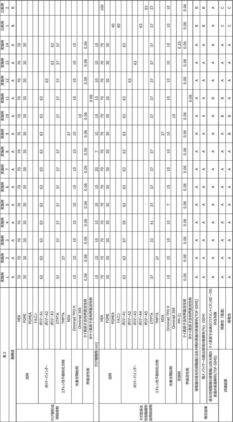
表2の結果から、実施例の転写フィルムは、現像性に優れるとともに、導電性に優れた導電パターンを有する積層体を形成できることが明らかである。
実施例1と実施例9の対比から、感光性樹脂層及び導電層が3官能以上のエチレン性不飽和化合物を含む場合(好ましくは3官能又は4官能のエチレン性不飽和化合物を含む場合)、導電パターンを有する積層体の導電性がより優れることが明らかである。
実施例1と実施例10の対比から、感光性樹脂層及び導電層が光重合開始剤としてアシルフォスフィンオキサイド系開始剤を含む場合(好ましくは2,4,6-トリメチルベンゾイル-ジフェニル-フォスフィンオキサイドを含む場合)、転写フィルムは、現像性により優れるとともに、導電パターンを有する積層体の導電性がより優れることが明らかである。
実施例1と実施例11の対比から、感光性樹脂層及び導電層がケイ素原子含有界面活性剤を含む場合(好ましくはポリエーテル変性シリコーンを含む場合)、転写フィルムは、現像性により優れることが明らかである。
実施例1と実施例9の対比から、感光性樹脂層及び導電層が3官能以上のエチレン性不飽和化合物を含む場合(好ましくは3官能又は4官能のエチレン性不飽和化合物を含む場合)、導電パターンを有する積層体の導電性がより優れることが明らかである。
実施例1と実施例10の対比から、感光性樹脂層及び導電層が光重合開始剤としてアシルフォスフィンオキサイド系開始剤を含む場合(好ましくは2,4,6-トリメチルベンゾイル-ジフェニル-フォスフィンオキサイドを含む場合)、転写フィルムは、現像性により優れるとともに、導電パターンを有する積層体の導電性がより優れることが明らかである。
実施例1と実施例11の対比から、感光性樹脂層及び導電層がケイ素原子含有界面活性剤を含む場合(好ましくはポリエーテル変性シリコーンを含む場合)、転写フィルムは、現像性により優れることが明らかである。
一方、比較例の転写フィルムでは、所望の要求を満たさないことが明らかである。
なお、比較例1及び比較例2のいずれにおいては、導電層の感光性樹脂層とは反対側の表面において、バインダーポリマー及びエチレン性不飽和化合物の両方が存在する状態ではなかった。
なお、比較例1及び比較例2のいずれにおいては、導電層の感光性樹脂層とは反対側の表面において、バインダーポリマー及びエチレン性不飽和化合物の両方が存在する状態ではなかった。
1 仮支持体
2 導電層
2a 導電パターン
3 感光性樹脂層
3a 硬化樹脂パターン
4 保護フィルム
5 マスクパターン
10、20 転写フィルム
22a 導電層2の感光性樹脂層とは反対側の表面
25 基板
30 積層体
L 活性光線
2 導電層
2a 導電パターン
3 感光性樹脂層
3a 硬化樹脂パターン
4 保護フィルム
5 マスクパターン
10、20 転写フィルム
22a 導電層2の感光性樹脂層とは反対側の表面
25 基板
30 積層体
L 活性光線
Claims (14)
- 仮支持体と、感光性樹脂層と、前記感光性樹脂層に隣接して配置される導電層と、を有する転写フィルムであり、
前記感光性樹脂層は、第1のバインダーポリマーと、第1のエチレン性不飽和基を有する化合物と、光重合開始剤とを含み、
前記導電層は、第2のバインダーポリマーと、第2のエチレン性不飽和基を有する化合物と、銀ナノワイヤーを含む導電性繊維とを含み、
前記導電層の前記感光性樹脂層とは反対側の表面に、前記第2のバインダーポリマーと、前記第2のエチレン性不飽和基を有する化合物とが存在する、転写フィルム。 - 前記仮支持体、前記導電層、及び前記感光性樹脂層をこの順に有する、請求項1に記載の転写フィルム。
- 前記導電層の前記感光性樹脂層とは反対側の表面における前記銀ナノワイヤーを含む導電性繊維が露出した領域の面積率が、20%以下である、請求項1又は2に記載の転写フィルム。
- 前記仮支持体の前記導電層及び前記感光性樹脂層を有する側とは反対側の面に、直径5μm以上の粒子が10個/mm2以上存在する、請求項1~3のいずれか1項に記載の転写フィルム。
- 前記第1のエチレン性不飽和基を有する化合物及び前記第2のエチレン性不飽和基を有する化合物が、分子中にエチレン性不飽和基を3又は4個含む、請求項1~4のいずれか1項に記載の転写フィルム。
- 前記第1のエチレン性不飽和基を有する化合物及び前記第2のエチレン性不飽和基を有する化合物が、エステル結合を含む、請求項1~5のいずれか1項に記載の転写フィルム。
- 前記第1のバインダーポリマーと前記第2のバインダーポリマーとが同じバインダーポリマーであり、且つ、前記第1のエチレン性不飽和基を有する化合物と前記第2のエチレン性不飽和基を有する化合物とが同じエチレン性不飽和基を有する化合物である、請求項1~6のいずれか1項に記載の転写フィルム。
- 前記感光性樹脂層が、更に、リン酸エステル化合物を含む、請求項1~7のいずれか1項に記載の転写フィルム。
- 前記光重合開始剤の含有量が、前記第1のエチレン性不飽和基を有する化合物の含有量に対して、質量比で0.05~0.5である、請求項1~8のいずれか1項に記載の転写フィルム。
- 前記感光性樹脂層の前記導電層とは反対側の表面にケイ素原子が存在する、請求項1~9のいずれか1項に記載の転写フィルム。
- 基板及び導電パターンを有する積層体の製造方法であって、
請求項1~10のいずれか1項に記載の転写フィルムと前記基板とを、前記転写フィルムの仮支持体が配置されている面とは反対側の面に前記基板を接触させて貼り合わせる工程と、
前記転写フィルムが有する感光性樹脂層をパターン露光する工程と、
前記転写フィルムが有する導電層の一部を、前記感光性樹脂層の未露光部とともに除去して、パターン状の導電層と、パターン状の硬化樹脂層を形成する工程と、を含む、積層体の製造方法。 - 請求項11に記載の製造方法で製造された積層体であって、
前記基板と、前記パターン状の導電層と、前記パターン状の硬化樹脂層とを有する、積層体。 - 請求項12に記載の積層体を有するタッチパネルセンサー。
- 請求項13に記載のタッチパネルセンサーを有するタッチパネル。
Priority Applications (2)
| Application Number | Priority Date | Filing Date | Title |
|---|---|---|---|
| JP2021550454A JPWO2021065288A1 (ja) | 2019-09-30 | 2020-09-01 | |
| CN202080064145.1A CN114401838A (zh) | 2019-09-30 | 2020-09-01 | 转印膜、层叠体的制造方法、层叠体、触摸面板传感器、触摸面板 |
Applications Claiming Priority (2)
| Application Number | Priority Date | Filing Date | Title |
|---|---|---|---|
| JP2019180500 | 2019-09-30 | ||
| JP2019-180500 | 2019-09-30 |
Publications (1)
| Publication Number | Publication Date |
|---|---|
| WO2021065288A1 true WO2021065288A1 (ja) | 2021-04-08 |
Family
ID=75337920
Family Applications (1)
| Application Number | Title | Priority Date | Filing Date |
|---|---|---|---|
| PCT/JP2020/033031 Ceased WO2021065288A1 (ja) | 2019-09-30 | 2020-09-01 | 転写フィルム、積層体の製造方法、積層体、タッチパネルセンサー、タッチパネル |
Country Status (3)
| Country | Link |
|---|---|
| JP (1) | JPWO2021065288A1 (ja) |
| CN (1) | CN114401838A (ja) |
| WO (1) | WO2021065288A1 (ja) |
Citations (3)
| Publication number | Priority date | Publication date | Assignee | Title |
|---|---|---|---|---|
| JP2012169072A (ja) * | 2011-02-10 | 2012-09-06 | Fujifilm Corp | 導電膜形成用積層体、導電膜形成方法、導電膜、導電要素、タッチパネル及び集積型太陽電池 |
| JP2017201354A (ja) * | 2016-05-02 | 2017-11-09 | 日立化成株式会社 | 感光性導電フィルム、導電パターンの形成方法、導電パターン基板及びタッチパネルセンサ |
| JP2017207536A (ja) * | 2016-05-16 | 2017-11-24 | 日立化成株式会社 | 感光性導電フィルム、フィルムセット、及び積層体の製造方法 |
-
2020
- 2020-09-01 CN CN202080064145.1A patent/CN114401838A/zh not_active Withdrawn
- 2020-09-01 WO PCT/JP2020/033031 patent/WO2021065288A1/ja not_active Ceased
- 2020-09-01 JP JP2021550454A patent/JPWO2021065288A1/ja not_active Ceased
Patent Citations (3)
| Publication number | Priority date | Publication date | Assignee | Title |
|---|---|---|---|---|
| JP2012169072A (ja) * | 2011-02-10 | 2012-09-06 | Fujifilm Corp | 導電膜形成用積層体、導電膜形成方法、導電膜、導電要素、タッチパネル及び集積型太陽電池 |
| JP2017201354A (ja) * | 2016-05-02 | 2017-11-09 | 日立化成株式会社 | 感光性導電フィルム、導電パターンの形成方法、導電パターン基板及びタッチパネルセンサ |
| JP2017207536A (ja) * | 2016-05-16 | 2017-11-24 | 日立化成株式会社 | 感光性導電フィルム、フィルムセット、及び積層体の製造方法 |
Also Published As
| Publication number | Publication date |
|---|---|
| JPWO2021065288A1 (ja) | 2021-04-08 |
| CN114401838A (zh) | 2022-04-26 |
Similar Documents
| Publication | Publication Date | Title |
|---|---|---|
| KR101348546B1 (ko) | 도전 패턴의 형성 방법, 도전 패턴 기판 및 터치 패널 센서 | |
| KR101255433B1 (ko) | 감광성 도전 필름, 도전막의 형성 방법, 도전 패턴의 형성 방법 및 도전막 기판 | |
| JP6176295B2 (ja) | 導電パターンの形成方法 | |
| JP6206028B2 (ja) | 導電パターンの製造方法、その方法により製造された導電パターンを備える導電パターン基板、その導電パターン基板を含むタッチパネルセンサ、及び感光性導電フィルム | |
| WO2016167228A1 (ja) | 感光性導電フィルム、導電パターンの形成方法、導電パターン付き基材、及びタッチパネルセンサ | |
| JP6205925B2 (ja) | 感光性導電フィルム、並びにこれを用いた導電パターンの形成方法及び導電パターン基板 | |
| WO2021065317A1 (ja) | 転写フィルム、積層体の製造方法、積層体、タッチパネルセンサー、タッチパネル | |
| JP5569144B2 (ja) | 感光性導電フィルム、導電膜の形成方法及び導電パターンの形成方法 | |
| WO2021065322A1 (ja) | 転写フィルム、積層体の製造方法、積層体、タッチパネルセンサー、タッチパネル | |
| WO2021039187A1 (ja) | 転写フィルム、転写フィルムの製造方法、積層体の製造方法、積層体、タッチパネルセンサー、タッチパネル | |
| TW201502704A (zh) | 感光性導電膜、及使用其的導電圖案的形成方法、導電圖案基板以及觸控面板感測器 | |
| WO2021065288A1 (ja) | 転写フィルム、積層体の製造方法、積層体、タッチパネルセンサー、タッチパネル | |
| JP2017198878A (ja) | 感光性導電フィルム及びそれを用いた導電パターン、導電パターン基板、タッチパネルセンサの製造方法 | |
| WO2021065331A1 (ja) | 転写フィルム、積層体の製造方法、積層体、タッチパネルセンサー、タッチパネル | |
| JP2017207536A (ja) | 感光性導電フィルム、フィルムセット、及び積層体の製造方法 | |
| JP2017156510A (ja) | 感光性導電フィルム、導電パターンの形成方法及び導電パターン基板、並びにタッチパネル | |
| JP2017201350A (ja) | 感光性導電フィルム、導電パターンの形成方法及び導電パターン基板の製造方法 | |
| JP2018022030A (ja) | 感光性導電フィルム、並びに、これを用いた導電パターンの形成方法、導電パターン基板及びタッチパネルセンサ | |
| JP2017201349A (ja) | 感光性導電フィルム、導電パターンの形成方法及び導電パターン基板の製造方法 | |
| JP2018040934A (ja) | 感光性導電フィルム、並びにこれを用いた導電パターン基板とその製造方法及びタッチパネルセンサ | |
| JP2018049055A (ja) | 感光性導電フィルム、導電パターンの形成方法及び導電パターン基板の形成方法 | |
| JP2018116841A (ja) | 導電層付き基材及びその製造方法、並びに、センサ | |
| WO2018138879A1 (ja) | 感光性導電フィルム、導電パターンの形成方法、導電パターン基材の製造方法、導電パターン基材、タッチパネルセンサ |
Legal Events
| Date | Code | Title | Description |
|---|---|---|---|
| 121 | Ep: the epo has been informed by wipo that ep was designated in this application |
Ref document number: 20872993 Country of ref document: EP Kind code of ref document: A1 |
|
| WWE | Wipo information: entry into national phase |
Ref document number: 2021550454 Country of ref document: JP |
|
| NENP | Non-entry into the national phase |
Ref country code: DE |
|
| 122 | Ep: pct application non-entry in european phase |
Ref document number: 20872993 Country of ref document: EP Kind code of ref document: A1 |