WO2021064816A1 - 下地基板及びその製造方法 - Google Patents
下地基板及びその製造方法 Download PDFInfo
- Publication number
- WO2021064816A1 WO2021064816A1 PCT/JP2019/038598 JP2019038598W WO2021064816A1 WO 2021064816 A1 WO2021064816 A1 WO 2021064816A1 JP 2019038598 W JP2019038598 W JP 2019038598W WO 2021064816 A1 WO2021064816 A1 WO 2021064816A1
- Authority
- WO
- WIPO (PCT)
- Prior art keywords
- film
- substrate
- layer
- orientation
- base substrate
- Prior art date
- Legal status (The legal status is an assumption and is not a legal conclusion. Google has not performed a legal analysis and makes no representation as to the accuracy of the status listed.)
- Ceased
Links
Images


Classifications
-
- C—CHEMISTRY; METALLURGY
- C30—CRYSTAL GROWTH
- C30B—SINGLE-CRYSTAL GROWTH; UNIDIRECTIONAL SOLIDIFICATION OF EUTECTIC MATERIAL OR UNIDIRECTIONAL DEMIXING OF EUTECTOID MATERIAL; REFINING BY ZONE-MELTING OF MATERIAL; PRODUCTION OF A HOMOGENEOUS POLYCRYSTALLINE MATERIAL WITH DEFINED STRUCTURE; SINGLE CRYSTALS OR HOMOGENEOUS POLYCRYSTALLINE MATERIAL WITH DEFINED STRUCTURE; AFTER-TREATMENT OF SINGLE CRYSTALS OR A HOMOGENEOUS POLYCRYSTALLINE MATERIAL WITH DEFINED STRUCTURE; APPARATUS THEREFOR
- C30B29/00—Single crystals or homogeneous polycrystalline material with defined structure characterised by the material or by their shape
- C30B29/10—Inorganic compounds or compositions
- C30B29/16—Oxides
Definitions
- the present invention relates to a base substrate used for crystal growth of a nitride or oxide of a Group 13 element and a method for producing the same.
- GaN gallium nitride
- MQW multiple quantum well layer in which a quantum well layer composed of an InGaN layer and a barrier layer composed of a GaN layer are alternately laminated, and a p-type GaN layer are sequentially laminated and formed. Is mass-produced.
- ⁇ -Ga 2 O 3 corundum phase type ⁇ -gallium oxide
- ⁇ -Ga 2 O 3 has a large bandgap of 5.3 eV, and is expected as a material for power semiconductor devices.
- Patent Document 1 Japanese Unexamined Patent Publication No. 2014-72533
- Patent Document 2 Japanese Unexamined Patent Publication No. 2016-25256 contains an n-type semiconductor layer containing a crystalline oxide semiconductor having a corundum structure as a main component and an inorganic compound having a hexagonal crystal structure as a main component.
- a semiconductor device provided with a p-type semiconductor layer and electrodes in an embodiment, ⁇ -Ga 2 O 3 having a corundum structure which is a semi-stable phase as an n-type semiconductor layer is mounted on a c-plane sapphire substrate as a p-type semiconductor. It is disclosed that an ⁇ -Rh 2 O 3 film having a hexagonal crystal structure is formed as a layer to produce a diode.
- the a-axis length (4.754 ⁇ ) of sapphire ( ⁇ -Al 2 O 3 ) and the a-axis length (4) of ⁇ -Ga 2 O 3 are formed. .983 ⁇ ) differs by about 5%, and this difference is the main cause of crystal defects.
- Non-Patent Document 1 Applied Physics Express, vol.9, pages 071101-1 to 071101-4
- Non-Patent Document 2 as a substrate for forming a alpha-Ga 2 O 3 film, a substrate obtained by forming an alpha-Cr 2 O 3 film as a buffer layer is disclosed on sapphire.
- Non-Patent Document 1 and Non-Patent Document 2 are insufficient for application to power semiconductors that require high dielectric breakdown electric field characteristics, and further reduces crystal defects. It is desirable to do. Even when ⁇ -Cr 2 O 3 as disclosed in Non-Patent Document 2 is formed as a buffer layer, it is insufficient for application to a power semiconductor that requires high dielectric breakdown electric field characteristics, and further crystal defects are added. It is desirable to reduce it.
- ⁇ -Cr 2 O 3 film When an ⁇ -Cr 2 O 3 film is used as the buffer layer, i) there is a lattice mismatch between ⁇ -Cr 2 O 3 and ⁇ -Ga 2 O 3 , and ii) a thin buffer layer is heterogeneous on sapphire. Since the structure is formed by epitaxial growth, it is presumed that the inclusion of large crystal defects in the buffer layer is the reason why the crystal defects cannot be sufficiently reduced.
- Partial peeling is one of the causes of warpage and cracks in the semiconductor layer.
- Partial peeling is one of the causes of warpage and cracks in the semiconductor layer.
- Such crystal defects and cracks in the semiconductor layer are greatly affected by the quality of the underlying substrate used for film formation.
- the present inventors have recently prepared an ⁇ -Cr 2 O 3 or ⁇ -Cr 2 O 3 system solid solution whose surface (orientation layer) used for crystal growth of a nitride or oxide of a group 13 element is ⁇ -Cr 2 O 3.
- ⁇ -Cr 2 O 3 or ⁇ -Cr 2 O 3 system solid solution whose surface (orientation layer) used for crystal growth of a nitride or oxide of a group 13 element is ⁇ -Cr 2 O 3.
- the alignment layer is made of a material containing Si and / or Ca as impurities in the ⁇ -Cr 2 O 3 or ⁇ -Cr 2 O 3 solid solution, so that the semiconductor layer formed on the alignment layer can be formed. It was found that the number of crystal defects is small and the alignment layer and the semiconductor layer can be made difficult to peel off at the time of film formation. In particular, in the crystal growth of a semiconductor film composed of ⁇ -Ga 2 O 3 or ⁇ -Ga 2 O 3 solid solution, the use of the above-mentioned base substrate has few crystal defects and is difficult to peel off during film formation. 2 O 3, or to obtain a finding that it is possible to form the formed semiconductor layer in ⁇ -Ga 2 O 3 solid solution.
- an object of the present invention is a substrate substrate provided with an orientation layer used for crystal growth of a nitride or oxide of a Group 13 element, and crystal defects of a semiconductor film to be formed on the substrate. It is an object of the present invention to provide a base substrate which can be made difficult to peel off at the time of film formation.
- a base substrate having an alignment layer used for the alpha-Ga 2 O 3, or alpha-Ga crystal growth of the semiconductor film composed of 2 O 3 solid solution
- a base substrate is provided in which the alignment layer is made of a material containing Mg in an ⁇ -Cr 2 O 3 or ⁇ -Cr 2 O 3 system solid solution.
- a base substrate is provided in which the alignment layer is made of a material containing Si and / or Ca in an ⁇ -Cr 2 O 3 or ⁇ -Cr 2 O 3 system solid solution.
- the method for manufacturing the base substrate is the method for manufacturing the base substrate.
- a method comprising a step of heat-treating the sapphire substrate and the alignment precursor layer at a temperature of 1000 ° C. or higher.
- the method for manufacturing the base substrate is the method for manufacturing the base substrate.
- the process of preparing the sapphire substrate and On the surface of the sapphire substrate, an orientation precursor layer containing a material containing Si and / or Ca in an ⁇ -Cr 2 O 3 or ⁇ -Cr 2 O 3 solid solution or a material having the above composition by heat treatment is provided.
- the process of forming and Provided is a method comprising a step of heat-treating the sapphire substrate and the alignment precursor layer at a temperature of 1000 ° C. or higher.
- the base substrate according to the present invention is a base substrate provided with an orientation layer used for crystal growth of nitrides or oxides of Group 13 elements. That is, this base substrate is a semiconductor film composed of a nitride or oxide of a Group 13 element on the alignment layer (particularly ⁇ -Ga 2 O 3 or ⁇ -Ga 2 O 3 solid solution). ) Is used to grow crystals.
- Group 13 elements are Group 13 elements according to the periodic table formulated by IUPAC (International Union of Pure and Applied Chemistry). Specifically, boron (B), indium (Al), and gallium (Ga). ), Indium (In), Thallium (Tl) and Nihonium (Nh).
- the nitrides and oxides of Group 13 elements are typically gallium nitride (GaN) and ⁇ -gallium oxide ( ⁇ -Ga 2 O 3 ).
- the orientation layer has a structure in which the crystal orientations are substantially aligned in the substantially normal direction. With such a configuration, it is possible to form a semiconductor layer having excellent quality, particularly excellent orientation, on the semiconductor layer. That is, when the semiconductor layer is formed on the oriented layer, the crystal orientation of the semiconductor layer generally follows the crystal orientation of the oriented layer. Therefore, the semiconductor film can be used as the alignment film by forming the base substrate with the alignment layer.
- the orientation layer may be a polycrystal, a mosaic crystal (a set of crystals whose crystal orientations are slightly deviated), or a single crystal.
- the oriented layer is polycrystalline, it is preferable that the oriented layer is a biaxially oriented layer in which the twist direction (that is, the rotation direction about the normal of the substrate oriented substantially perpendicular to the substrate surface) is also substantially aligned.
- the surface on the side used for crystal growth of the oriented layer (hereinafter, may be simply referred to as "surface” or “aligned layer surface”) is an ⁇ -Cr 2 O 3 or ⁇ -Cr 2 O 3 system solid solution (that is, that is). It is composed of a material containing (a solid solution of ⁇ -Cr 2 O 3 and a different material) as a main component and Mg as an impurity.
- Crystal defects in the semiconductor layer such as Ga 2 O 3 can be remarkably reduced, and the alignment layer and the semiconductor layer can be made difficult to peel off.
- the reason for the reduction of crystal defects in the semiconductor layer is unknown, but it is assumed as follows.
- the ⁇ -Cr 2 O 3 or ⁇ -Cr 2 O 3 system solid solution has a corundum structure, but its lattice constant does not completely match that of the semiconductor layer composed of nitrides or oxides of Group 13 elements. Therefore, when a semiconductor layer is formed on an ⁇ -Cr 2 O 3 or ⁇ -Cr 2 O 3 solid solution, stress due to lattice mismatch is applied, but by containing Mg in ⁇ -Cr 2 O 3. It is considered that the stress is relaxed and crystal defects are less likely to occur.
- the reason why the semiconductor layer is partially difficult to peel off is unknown, but it is presumed that one of the reasons is that the stress due to the lattice mismatch during film formation is relaxed as described above. Further, by containing Mg in the ⁇ -Cr 2 O 3 or ⁇ -Cr 2 O 3 system solid solution constituting the surface of the alignment layer, the electrical characteristics of the surface of the alignment layer are changed and the affinity with the semiconductor layer is changed. Is also expected to have the effect of increasing.
- the surface of the alignment layer on the side used for crystal growth contains ⁇ -Cr 2 O 3 or ⁇ -Cr 2 O 3 solid solution as a main component and contains Si and / or Ca as impurities. It is composed of materials.
- Such an oriented layer has the same effect as that of an oriented layer composed of a material containing the above-mentioned ⁇ -Cr 2 O 3 or ⁇ -Cr 2 O 3 solid solution as a main component and containing Mg as an impurity. That is, it is formed on the alignment layer composed of a material containing ⁇ -Cr 2 O 3 or ⁇ -Cr 2 O 3 solid solution as a main component and Si and / or Ca as impurities.
- Crystal defects in the semiconductor layer such as ⁇ -Ga 2 O 3 can be remarkably reduced, and the alignment layer and the semiconductor layer can be made difficult to peel off. The reason for this is unknown, but it is presumed that stress relaxation due to lattice mismatch and changes in the electrical characteristics of the surface of the oriented layer are acting as in the case of the oriented layer containing Mg as an impurity.
- the Mg content in the oriented layer composed of the ⁇ -Cr 2 O 3 or ⁇ -Cr 2 O 3 solid solution is 5 ⁇ 10 15 atoms / cm 3
- the above is preferable.
- the Mg content is too high, pits may occur on the surface of the semiconductor layer.
- the cause of the pit formation is unknown, but it is presumed that one of the reasons is that a portion having a locally high Mg concentration is formed in the substrate and the semiconductor layer becomes a region where it is difficult to form a film.
- the content of Mg in the ⁇ -Cr 2 O 3 or ⁇ -Cr 2 O 3 system solid solution is preferably 5 ⁇ 10 19 atoms / cm 3 or less. Therefore, from the viewpoint of achieving both partial peeling suppression and pit suppression of the semiconductor layer, the content of Mg in the oriented layer composed of the ⁇ -Cr 2 O 3 or ⁇ -Cr 2 O 3 system solid solution is 5 ⁇ . 10 15 to 5 ⁇ 10 19 atoms / cm 3 is preferable.
- the content of Si and Ca in the orientation layer composed of the ⁇ -Cr 2 O 3 or ⁇ -Cr 2 O 3 system solid solution contains Si. If this is the case, the Si content is preferably 1 ⁇ 10 16 atoms / cm 3 or more, and if Ca is contained, the Ca content is preferably 5 ⁇ 10 15 atoms / cm 3 or more. However, if the content of Si and / or Ca is too large, pits may occur on the surface of the semiconductor layer.
- the cause of the pit formation is unknown, but it is presumed that one of the reasons is that a portion having a locally high concentration of Si and / or Ca is formed in the base substrate, which makes it difficult for the semiconductor layer to form a film. Therefore, from the viewpoint of suppressing pits in the semiconductor layer, the content of Si and Ca in the orientation layer composed of the ⁇ -Cr 2 O 3 or ⁇ -Cr 2 O 3 solid solution is Si when Si is contained.
- the content of Ca is preferably 1 ⁇ 10 18 atoms / cm 3 or less, and when Ca is contained, the content of Ca is preferably 5 ⁇ 10 17 atoms / cm 3 or less.
- the content of Si and Ca in the alignment layer composed of the ⁇ -Cr 2 O 3 or ⁇ -Cr 2 O 3 system solid solution is high. If Si is contained, the Si content is 1 ⁇ 10 16 to 1 ⁇ 10 18 atoms / cm 3 , and if Ca is contained, the Ca content is 5 ⁇ 10 15 to 5 ⁇ 10 17 atoms / cm 3. Is preferable.
- the orientation layer composed of the ⁇ -Cr 2 O 3 or ⁇ -Cr 2 O 3 solid solution is i) If only Si is detected in the oriented layer (eg by SIMS analysis), the Si content is 1 ⁇ 10 16 to 1 ⁇ 10 18 atoms / cm 3 , ii) If only Ca in the alignment layer is detected (e.g., by SIMS analysis), the content of Ca is 5 ⁇ 10 15 ⁇ 5 ⁇ 10 17 atoms / cm 3, or, iii) When Si and Ca are detected in the oriented layer (eg by SIMS analysis), the Si content is 1 ⁇ 10 16 to 1 ⁇ 10 18 atoms / cm 3 , and the Ca content is 5 ⁇ 10 15 ⁇ 5 ⁇ 10 17 atoms / cm 3 , It is preferable to satisfy the relationship of.
- the alignment layer preferably contains not only Mg but also Si and / or Ca in the ⁇ -Cr 2 O 3 or ⁇ -Cr 2 O 3 system solid solution. In that case, it is preferable that each of the Si content and the Ca content in the alignment layer is smaller than the Mg content. By doing so, it is possible to make it more difficult for the semiconductor layer to be partially peeled off.
- the content of Mg, Si and Ca in the alignment layer can be determined by using a known method, and for example, EDS, EPMA, D-SIMS, TOF-SIMS and GD-MS can be used. Of these, D-SIMS is preferable.
- the half-value width of the X-ray locking curve (hereinafter referred to as the XRC half-value width) of the (104) plane of the corundum-type crystal structure on the surface used for crystal growth of the alignment layer of the base substrate of the present invention is 500 arcsec.
- the following is preferable, and 150 arcsec.
- the following is more preferable, and 100 arcsec.
- the following is more preferable, and 50 arcsec.
- the following are particularly preferable, and most preferably 40 arcsec. It is as follows.
- a method for evaluating the crystallinity of a material As a method for evaluating the crystallinity of a material, a method is known in which XRC measurement of the (006) plane and the (104) plane of a corundum type crystal structure is carried out and the evaluation is performed in the half price range.
- the XRC full width at half maximum also reflects crystal defects, mosaic properties, and the amount of warpage of the material.
- the XRC full width at half maximum of the (104) plane of the corundum-type crystal structure includes various defects such as penetrating blade-shaped dislocations and penetrating spiral dislocations, tilt (tilt of the crystal axis in the growth direction), and twist (rotation of the crystal axis in the surface surface).
- the quality of the oriented layer is suitable as an evaluation method. Therefore, if the XRC range width is within the above range, the oriented layer has few crystal defects, low mosaic properties (less domains), and small warpage, and as a result, ⁇ - on such an oriented layer.
- a semiconductor layer such as Ga 2 O 3 is formed, a high-quality semiconductor layer in which crystal defects and mosaic properties do not propagate inside the semiconductor layer and the warp is small can be obtained.
- the XRC profile of the (104) plane of the corundum-type crystal structure on the surface used for crystal growth of the alignment layer can be measured using a general XRD apparatus.
- This measurement is preferably performed after converting CuK ⁇ rays into parallel monochromatic light with a Ge (022) asymmetric reflection monochromator. Then, the half width in the XRC profile of the (104) plane of the corundum type crystal structure is peak-searched after smoothing the profile using XRD analysis software (Made by Bruker-AXS, "LEPTOS” Ver4.03). It can be decided by.
- the XRC half width of the (006) plane of the corundum type crystal structure on the surface used for crystal growth of the alignment layer is also small, preferably 50 arcsec. Hereinafter, more preferably, 40 arcsec. It is as follows.
- the XRC half-value width of the (006) plane of the corundum-type crystal structure may be the same as the half-value width peculiar to the X-ray source used for the measurement, but there is no problem, but in reality, 30 arcsec. The above is preferable.
- the XRC full width at half maximum of the (006) plane of the corundum-type crystal structure reflects information on penetrating spiral dislocations, tilts and warpages, and domains.
- the XRC full width at half maximum is within the above range, there are few crystal defects, the mosaic property is small (the domain is small), and the warp is also small, and as a result, a semiconductor layer is formed on such an oriented layer. In this case, crystal defects and domains do not propagate inside the semiconductor layer, and a higher quality semiconductor layer can be obtained.
- the XRC profile of the (006) plane of the corundum-type crystal structure with respect to the surface on the side used for crystal growth of the alignment layer can also be measured using a general XRD apparatus.
- the crystal defect density on the surface of the surface used for crystal growth of the alignment layer is preferably 1.0 ⁇ 10 6 / cm 2 or less, more preferably 1.0 ⁇ 10 5 / cm. It is 2 or less, more preferably 4.0 ⁇ 10 3 / cm 2 or less, and particularly preferably 1.0 ⁇ 10 3 / cm 2 or less.
- a high-quality semiconductor layer having excellent dielectric breakdown electric field characteristics does not propagate in the semiconductor layer such as ⁇ -Ga 2 O 3 formed on the film-formed surface. Can be obtained.
- the lower limit of the crystal defect density is not particularly limited, and a lower limit is preferable.
- the crystal defect refers to a through-blade dislocation, a through-spiral dislocation, a through-mixed dislocation, and a basal plane dislocation
- the crystal defect density is the total of each dislocation density.
- the basal plane dislocation is a problem when the semiconductor film has an off-angle, and is not a problem because the surface of the semiconductor film is not exposed when there is no off-angle.
- the penetrating blade dislocations are 3 ⁇ 10 4 / cm 2
- the penetrating spiral dislocations are 6 ⁇ 10 4 / cm 2
- the penetrating mixed dislocations are 4 ⁇ 10 4 / cm 2
- the crystal defect density is 1.3. It becomes ⁇ 10 5 / cm 2.
- the crystal defect density on the surface of the oriented layer used for crystal growth can be evaluated by planar TEM observation (plan view).
- plane TEM observation When performing plane TEM observation, it can be performed using a general transmission electron microscope. For example, when a Hitachi H-90001UHR-I is used as a transmission electron microscope, TEM observation may be performed at an acceleration voltage of 300 kV.
- a sample is cut out so as to include the surface on the side used for crystal growth of the alignment layer, and eight or more regions with a measurement field of view of 4.1 ⁇ m ⁇ 3.1 ⁇ m can be observed around the measurement field of view. It may be processed by ion milling so that the thickness of is 150 nm.
- the crystal defect density can be evaluated from the planar TEM image of the surface of the test piece thus obtained.
- the entire alignment layer is made of a material having a corundum-type crystal structure. By doing so, it is possible to reduce crystal defects in the alignment layer and the semiconductor layer.
- the alignment layer is preferably formed on the surface of the sapphire substrate.
- the ⁇ -Al 2 O 3 constituting the sapphire substrate has a corundum-type crystal structure, and by configuring the alignment layer with a material having a corundum-type crystal structure, the crystal structure can be made the same as that of the sapphire substrate.
- the crystal defects in the alignment layer are reduced because the crystal defects in the semiconductor layer formed on the crystal defects are also reduced. This is because when a large amount of crystal defects are present in the alignment layer, the crystal defects are inherited by the semiconductor layer formed on the crystal defects, and as a result, crystal defects are also generated in the semiconductor layer.
- the thickness of the alignment layer is preferably 10 ⁇ m or more, more preferably 40 ⁇ m or more.
- the upper limit of the thickness is not particularly limited, but is typically 1000 ⁇ m or less.
- it may be thicker from the viewpoint of handleability, for example, 1 mm or more, but from the viewpoint of cost, it is, for example, 2 mm or less.
- the alignment layer When the alignment layer is formed on the sapphire substrate, the lattice constants of the sapphire substrate and the alignment layer are slightly different, and as a result, crystal defects are likely to occur at these interfaces, that is, the lower part of the alignment layer.
- the alignment layer thicker, it is possible to reduce the influence of crystal defects generated in the lower part of the alignment layer on the surface of the alignment layer. The reason for this is not clear, but it is thought that the crystal defects generated in the lower part of the alignment layer do not reach the surface of the thick alignment layer and disappear.
- the alignment layer thicker, it is expected that after the semiconductor layer is formed on the alignment layer, the semiconductor layer can be peeled off and the underlying substrate can be reused.
- the alignment layer is formed on the sapphire substrate, it is preferable that an inclined composition region whose composition changes in the thickness direction exists in the alignment layer.
- the inclined composition region is composed of a solid solution of ⁇ -Al 2 O 3 and a material constituting the surface of the oriented layer on the side used for crystal growth, and the solid solution amount of ⁇ -Al 2 O 3 is sapphire. It is preferable to provide a region (inclined composition region) having an inclined composition that decreases from the substrate side toward the surface side of the alignment layer.
- Graded composition region is preferably composed of a solid solution containing ⁇ -Al 2 O 3 and ⁇ -Cr 2 O 3, in particular, including the ⁇ -Al 2 O 3 and ⁇ -Cr 2 O 3 Si and / or Ca It is preferably composed of a solid solution. That is, it is desirable that the alignment layer is formed on the surface of the sapphire substrate, but the stress due to the difference in lattice constant (a-axis length and / or c-axis length) between the sapphire substrate and the alignment layer is relaxed, and the occurrence of crystal defects is suppressed.
- the a-axis length and / or c-axis length is different between the front surface and the back surface of the alignment layer, and it is preferable that the front surface has a larger a-axis length and / or c-axis length than the back surface of the alignment layer.
- Such an inclined composition region can be formed by heat-treating the sapphire substrate and the orientation precursor layer at a temperature of 1000 ° C. or higher in the production of the base substrate described later. That is, when the heat treatment is performed at such a high temperature, a reaction occurs at the interface between the sapphire substrate and the alignment precursor layer, and the Al component in the sapphire substrate diffuses into the alignment precursor layer, or the component in the alignment precursor layer becomes. It diffuses into the sapphire substrate. As a result, an inclined composition region in which the solid solution amount of ⁇ -Al 2 O 3 changes in the thickness direction is formed. A thicker inclined composition region is preferable because stress due to a difference in lattice constant is more likely to be relaxed.
- the thickness of the inclined composition region is preferably 5 ⁇ m or more, more preferably 20 ⁇ m or more.
- the upper limit of the thickness is not particularly limited, but is typically 1000 ⁇ m or less.
- the orientation layer changes in the thickness direction, which is located near the surface and has a stable composition in the thickness direction, and is located far from the surface. It has an inclined composition region.
- the composition stable region is a region in which the change in the content ratio of each metal element is less than 1.0 at%
- the inclined composition region is a region in which the change in the content ratio of each metal element is 1.0 at% or more. ..
- the composition stable region and the inclined composition region can be determined as follows. First, a cross-sectional sample of the alignment layer is prepared, energy dispersive X-ray analysis (EDS) is performed at any 10 locations near the surface of the alignment layer, and the average value of the detected metal element content ratio (at%) is calculated.
- EDS energy dispersive X-ray analysis
- the region from the surface to the thickness of 2 ⁇ m can be assigned to either the composition stable region or the inclined composition region.
- the attribution of the area between the points can be determined.
- the region between the point having a thickness of 24 ⁇ m and the point having a thickness of 26 ⁇ m from the surface can be determined to be assigned by calculating the average value of the metal element content ratio at each point and comparing them. Then, for example, when Al is contained in the alignment layer, it is more preferable that the Al concentration in the inclined composition region decreases in the thickness direction toward the composition stable region.
- the material having a corundum-type crystal structure is a material containing Mg as an impurity in ⁇ -Cr 2 O 3 , or ⁇ -Al 2 O 3 and ⁇ -Cr 2 O 3 . It is preferably a solid solution of a material containing Mg as an impurity.
- the material having a corundum-type crystal structure (for example, a gradient composition region) contains Si and / or Ca as impurities in ⁇ -Cr 2 O 3 , or ⁇ -Al 2 O 3 and It is preferably a solid solution of a material containing Si and / or Ca as impurities in ⁇ -Cr 2 O 3.
- the inclined composition region contains Mg as an impurity in ⁇ -Cr 2 O 3 , and a material containing Si and / or Ca in a smaller amount than Mg, or impurities in ⁇ -Al 2 O 3 and ⁇ -Cr 2 O 3. It is composed of Mg and a solid solution of a material containing Si and / or Ca in a smaller amount than Mg.
- the material constituting the alignment layer is not particularly limited as long as it has orientation with respect to the surface of the base substrate, and is, for example, c-axis orientation, a-axis orientation, or m-axis orientation. By doing so, when the semiconductor layer is formed on the base substrate, the semiconductor film can be oriented in the c-axis orientation film, the a-axis alignment film, or the m-axis alignment film.
- the orientation layer is preferably a heteroepitaxial growth layer.
- both the sapphire substrate and the alignment layer have a corundum-type crystal structure. Therefore, when these lattice constants are close to each other, the crystal plane of the alignment layer is sapphire during heat treatment.
- Epitaxial growth may occur in which the substrate is arranged according to the crystal orientation of the substrate. By epitaxially growing the oriented layer in this way, it becomes possible to inherit the high crystallinity and crystal orientation peculiar to a single crystal of the sapphire substrate to the oriented layer.
- the arithmetic mean roughness Ra on the surface of the alignment layer is preferably 1 nm or less, more preferably 0.5 nm or less, and further preferably 0.2 nm or less.
- the base substrate has an area of preferably 20 cm 2 or more, more preferably 70 cm 2 or more, and further preferably 170 cm 2 or more on one side thereof.
- the upper limit of the size is not particularly limited, but is typically 700 cm 2 or less on one side.
- the substrate of the present invention preferably further includes a support substrate on the side opposite to the front surface (that is, the back surface side) of the alignment layer.
- the base substrate of the present invention can be a base substrate including a support substrate and an alignment layer provided on the support substrate.
- the support substrate is preferably a corundum single crystal such as a sapphire substrate or Cr 2 O 3 , and a sapphire substrate is particularly preferable.
- a corundum single crystal as the support substrate, it is possible to serve as a seed crystal for heteroepitaxial growth of the oriented layer. Further, by forming the structure including the corundum single crystal in this way, it is possible to obtain a semiconductor layer having excellent quality.
- the corundum single crystal has characteristics such as excellent mechanical properties, thermal properties, and chemical stability.
- sapphire has a high thermal conductivity of 42 W / m ⁇ K at room temperature and is excellent in thermal conductivity. Therefore, by using a base substrate provided with a sapphire substrate, it is possible to improve the thermal conductivity of the entire substrate. As a result, when a semiconductor layer is formed on the substrate, it is expected that the temperature distribution in the substrate surface will be suppressed from becoming non-uniform, and a semiconductor layer having a uniform film thickness can be obtained. .. Further, although the sapphire substrate has a large area, it is easily available, the overall cost can be reduced, and a semiconductor layer having a large area can be obtained.
- the sapphire substrate used as the support substrate may have any orientation plane. That is, it may have a-plane, c-plane, r-plane, and m-plane, and may have a predetermined off-angle with respect to these planes. Further, sapphire to which a dopant is added may be used in order to adjust the electrical characteristics. Known dopants can be used as such dopants.
- a semiconductor layer composed of nitrides or oxides of Group 13 elements by using the orientation layer of the base substrate according to the present invention.
- Known methods can be used for forming the semiconductor layer, but various CVD methods, HVPE methods, sublimation methods, MBE methods, PLD methods, sputtering methods and other vapor phase film formation methods, hydrothermal methods, Na flux methods and the like can be used. Any of the liquid phase film formation methods is preferable.
- the CVD method include a thermal CVD method, a plasma CVD method, a mist CVD method, an MO (organic metal) CVD method, and the like. Among these, the mist CVD method, the hydrothermal method, or the HVPE method is particularly preferable for forming the semiconductor layer composed of the oxide of the group 13 element.
- the base substrate of the present invention may be in the form of a self-standing substrate with a single alignment layer, or may be in the form of a base substrate with a support substrate such as a sapphire substrate. Therefore, if necessary, the alignment layer may be finally separated from a support substrate such as a sapphire substrate.
- the separation of the support substrate may be performed by a known method and is not particularly limited. For example, a method of applying a mechanical impact to separate the oriented layer, a method of applying heat to separate the oriented layer using thermal stress, a method of applying vibration such as ultrasonic waves to separate the oriented layer, and a method of separating unnecessary parts.
- the alignment layer may be installed on another support substrate after the sapphire substrate is separated.
- the material of the other support substrate is not particularly limited, but a suitable material may be selected from the viewpoint of material physical characteristics. For example, from the viewpoint of thermal conductivity, metal substrates and substrates such as Cu, ceramic substrates such as SiC and AlN, and the like can be mentioned.
- a sapphire substrate is prepared, (b) a predetermined orientation precursor layer is prepared, and (c) the orientation precursor layer is heat-treated on the sapphire substrate to at least the sapphire substrate. It can be preferably produced by converting a nearby portion into an alignment layer and, if desired, subjecting it to processing such as (d) grinding or polishing to expose the surface of the alignment layer.
- the alignment precursor layer is to be a seed layer by heat treatment, ⁇ -Cr 2 O 3 or ⁇ -Cr 2 O 3 based solid solution in the material containing Mg or by heat treatment to be described later, ⁇ -Cr 2 O 3
- the ⁇ -Cr 2 O 3 system solid solution contains a material that contains Mg.
- the orientation precursor layer may contain trace components in addition to the material having a corundum-type crystal structure and Mg. According to such a manufacturing method, the growth of the alignment layer can be promoted by using the sapphire substrate as a seed crystal. That is, the high crystallinity and crystal orientation orientation peculiar to a single crystal of a sapphire substrate are inherited by the alignment layer.
- the alignment precursor layer becomes an alignment layer by heat treatment, and is a material containing Si and / or Ca in an ⁇ -Cr 2 O 3 or ⁇ -Cr 2 O 3 system solid solution, or It contains a material that is a material containing Si and / or Ca in an ⁇ -Cr 2 O 3 or ⁇ -Cr 2 O 3 system solid solution by the heat treatment described later.
- the orientation precursor layer may contain trace components in addition to the material having a corundum-type crystal structure and Si and / or Ca.
- the production method when Mg is contained as an impurity in the alignment layer will be illustrated, but the same production method will be used when Si and / or Ca is contained, and when Mg and a smaller amount of Si and / or Ca than Mg are contained. Can be used.
- a sapphire substrate is prepared.
- the sapphire substrate used may have any orientation plane. That is, it may have a-plane, c-plane, r-plane, and m-plane, and may have a predetermined off-angle with respect to these planes.
- c-plane sapphire since it is c-axis oriented with respect to the surface, an oriented layer oriented c-axis can be easily heteroepitaxially grown on the c-axis oriented layer.
- a sapphire substrate to which a dopant has been added in order to adjust the electrical characteristics. Known dopants can be used as such dopants.
- orientation precursor layer containing a material to be a material containing Mg is prepared.
- the method for forming the orientation precursor layer is not particularly limited, and a known method can be adopted. Examples of methods for forming the orientation precursor layer include AD (aerosol deposition) method, sol-gel method, hydrothermal method, sputtering method, thin-film deposition method, various CVD (chemical vapor deposition) methods, HVPE method, PLD method, etc.
- Examples include the CVT (chemical vapor deposition) method and the sublimation method.
- Examples of the CVD method include a thermal CVD method, a plasma CVD method, a mist CVD method, an MO (organic metal) CVD method, and the like.
- a method may be used in which a molded product of the orientation precursor is prepared in advance and the molded product is placed on a sapphire substrate.
- Such a molded product can be produced by molding the material of the orientation precursor by a method such as tape molding or press molding.
- the aerosol deposition (AD) method various CVD methods, or sputtering methods are preferable.
- AD aerosol deposition
- various CVD methods various CVD methods
- sputtering methods are preferable.
- the sputtering method it is possible to form a film using a target made of the same material as the alignment precursor layer, but it is also possible to use a reactive sputtering method in which a metal target is used to form a film in an oxygen atmosphere. it can.
- a method of placing the molded product prepared in advance on sapphire is also preferable as a simple method, but since the orientation precursor layer is not dense, a process of densification is required in the heat treatment step described later.
- the method using a polycrystalline body prepared in advance as the orientation precursor layer requires two steps, a step of preparing the polycrystalline body and a step of heat treatment on the sapphire substrate. Further, in order to improve the adhesion between the polycrystal and the sapphire substrate, it is necessary to take measures such as keeping the surface of the polycrystal sufficiently smooth.
- known conditions can be used for either method, a method of directly forming an orientation precursor layer using the AD method and a method of placing a prefabricated molded product on a sapphire substrate will be described below. ..
- the AD method is a technology in which fine particles and fine particle raw materials are mixed with gas to form an aerosol, and this aerosol is jetted at high speed from a nozzle to collide with a substrate to form a film, which is said to be able to form a densified film at room temperature. It has characteristics.
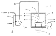
- FIG. 1 shows an example of a film forming apparatus (aerosol deposition (AD) apparatus) used in such an AD method.
- the film forming apparatus 20 shown in FIG. 1 is configured as an apparatus used in the AD method of injecting raw material powder onto a substrate in an atmosphere of atmospheric pressure lower than atmospheric pressure.
- the film forming apparatus 20 includes an aerosol generation unit 22 that generates an aerosol of a raw material powder containing a raw material component, and a film forming unit 30 that injects the raw material powder onto a sapphire substrate 21 to form a film containing the raw material component.
- the aerosol generation unit 22 includes an aerosol generation chamber 23 that stores raw material powder and receives a carrier gas supply from a gas cylinder (not shown) to generate an aerosol, and a raw material supply pipe 24 that supplies the generated aerosol to the film forming unit 30.
- the aerosol generation chamber 23 and the aerosol in the aerosol are provided with a vibration exciter 25 that vibrates at a frequency of 10 to 100 Hz.
- the film-forming unit 30 has a film-forming chamber 32 that injects aerosols onto the sapphire substrate 21, a substrate holder 34 that is arranged inside the film-forming chamber 32 and fixes the sapphire substrate 21, and a substrate holder 34 on the X-axis-Y-axis. It is equipped with an XY stage 33 that moves in a direction. Further, the film forming section 30 includes an injection nozzle 36 in which a slit 37 is formed at the tip thereof to inject aerosol into the sapphire substrate 21, and a vacuum pump 38 for reducing the pressure in the film forming chamber 32.
- the AD method can control the film thickness, film quality, etc. depending on the film forming conditions.
- the form of the AD film is easily affected by the collision rate of the raw material powder with the substrate, the particle size of the raw material powder, the aggregated state of the raw material powder in the aerosol, the injection amount per unit time, and the like.
- the collision speed of the raw material powder with the substrate is affected by the differential pressure between the film forming chamber 32 and the injection nozzle 36, the opening area of the injection nozzle, and the like. If appropriate conditions are not used, the coating may become a green compact or form pores, so it is necessary to appropriately control these factors.
- the raw material powder of the orientation precursor can be molded to prepare the molded product.
- the orientation precursor layer is a press molded body.
- the press-molded product can be produced by press-molding the raw material powder of the orientation precursor based on a known method.
- the raw material powder is placed in a mold, preferably 100 to 400 kgf / cm 2 , more preferably 150. It may be produced by pressing at a pressure of about 300 kgf / cm 2.
- the molding method is not particularly limited, and in addition to press molding, tape molding, casting molding, extrusion molding, doctor blade method, and any combination thereof can be used.
- additives such as a binder, a plasticizer, a dispersant, and a dispersion medium are appropriately added to the raw material powder to form a slurry, and the slurry is passed through a narrow slit-shaped discharge port to form a sheet. It is preferable to discharge and mold.
- the thickness of the molded product formed into a sheet is not limited, but is preferably 5 to 500 ⁇ m from the viewpoint of handling. Further, when a thick orientation precursor layer is required, a large number of these sheet molded products may be stacked and used as a desired thickness.
- the portion near the sapphire substrate becomes an orientation layer by the subsequent heat treatment on the sapphire substrate.
- the molded product may contain trace components such as a sintering aid in addition to the material having or bringing about a corundum-type crystal structure.
- (C) Heat treatment of the alignment precursor layer on the sapphire substrate The sapphire substrate on which the alignment precursor layer is formed is heat-treated at a temperature of 1000 ° C. or higher. By this heat treatment, at least a portion of the alignment precursor layer near the sapphire substrate can be converted into a dense alignment layer. Further, this heat treatment enables heteroepitaxial growth of the oriented layer. That is, by forming the alignment layer with a corundum material containing Mg in an ⁇ -Cr 2 O 3 or ⁇ -Cr 2 O 3 system solid solution, heteroepitaxial growth occurs in which the sapphire substrate is used as a seed crystal during heat treatment to grow crystals.
- the crystals are rearranged, and the crystals are arranged according to the crystal plane of the sapphire substrate.
- the crystal axes of the sapphire substrate and the alignment layer can be aligned.
- the sapphire substrate and the alignment layer can both be oriented in the c-axis with respect to the surface of the base substrate.
- this heat treatment makes it possible to form an inclined composition region in a part of the alignment layer.
- a gradient composition region composed of a solid solution containing ⁇ -Al 2 O 3 is formed.
- the orientation precursor layer is in a non-oriented state at the time of its production, that is, it is an amorphous or non-oriented polycrystal, and it is preferable to cause crystal rearrangement using sapphire as a seed crystal during this heat treatment step. By doing so, it is possible to effectively reduce the crystal defects that reach the surface of the alignment layer. The reason for this is not clear, but it is thought that the crystal defects generated in the lower part of the alignment layer are likely to be annihilated.
- the heat treatment is not particularly limited as long as a material containing Mg in an ⁇ -Cr 2 O 3 or ⁇ -Cr 2 O 3 solid solution is obtained and heteroepitaxial growth occurs using a sapphire substrate as a seed, and the heat treatment is not particularly limited, such as a tube furnace or a hot plate. , Can be carried out in a known heat treatment furnace. Further, in addition to these heat treatments under normal pressure (pressless), pressure heat treatments such as hot press and HIP, and combinations of normal pressure heat treatments and pressure heat treatments can also be used.
- the heat treatment conditions can be appropriately selected depending on the material used for the alignment layer.
- the heat treatment atmosphere can be selected from air, vacuum, nitrogen and an inert gas atmosphere.
- the preferred heat treatment temperature also varies depending on the material used for the alignment layer, but is preferably 1000 to 2000 ° C, more preferably 1200 to 2000 ° C, for example.
- the heat treatment temperature and holding time are related to the thickness of the alignment layer generated by heteroepitaxial growth and the thickness of the inclined composition region formed by diffusion with the sapphire substrate. It can be adjusted as appropriate depending on the size and the like. However, when a prefabricated molded product is used as an orientation precursor layer, it is necessary to sinter and densify it during heat treatment, and atmospheric firing at high temperature, hot pressing, HIP, or a combination thereof is preferable. ..
- the surface pressure is preferably 50 kgf / cm 2 or more, more preferably 100 kgf / cm 2 or more, particularly preferably 200 kgf / cm 2 or more, the upper limit is not particularly limited.
- the firing temperature is also not particularly limited as long as sintering, densification, and heteroepitaxial growth occur, but is preferably 1000 ° C. or higher, more preferably 1200 ° C. or higher, further preferably 1400 ° C. or higher, and particularly preferably 1600 ° C. or higher.
- the firing atmosphere can also be selected from atmosphere, vacuum, nitrogen and an inert gas atmosphere.
- the firing jig such as a mold, those made of graphite or alumina can be used.
- an oriented precursor layer or a surface layer having poor or unoriented orientation may exist or remain.
- the surface derived from the alignment precursor layer is subjected to processing such as grinding or polishing to expose the surface of the alignment layer.
- processing such as grinding or polishing to expose the surface of the alignment layer.
- a material having excellent orientation is exposed on the surface of the alignment layer, so that the semiconductor layer can be effectively epitaxially grown on the material.
- the method for removing the orientation precursor layer and the surface layer is not particularly limited, and examples thereof include a method for grinding and polishing and a method for ion beam milling.
- the surface of the alignment layer is preferably polished by lapping using abrasive grains or chemical mechanical polishing (CMP).
- CMP chemical mechanical polishing
- Semiconductor layer It is possible to form a semiconductor layer made of a nitride or oxide of a group 13 element by using the base substrate of the present invention.
- a known method can be used for forming the semiconductor layer, but various CVD methods, HVPE methods, sublimation methods, MBE methods, PLD methods, sputtering methods and other vapor deposition methods, hydrothermal methods, Na flux methods and the like can be used. Any of the liquid phase film forming methods is preferable, and the mist CVD method, the hydrothermal method, or the HVPE method is particularly preferable. The mist CVD method will be described below.
- the raw material solution is atomized or dropletized to generate mist or droplets, and the mist or droplet is conveyed to a film forming chamber equipped with a substrate using a carrier gas, and the mist or droplet is transferred in the film forming chamber.
- a film forming chamber equipped with a substrate using a carrier gas, and the mist or droplet is transferred in the film forming chamber.
- FIG. 2 shows an example of a mist CVD apparatus.
- a control valve 3a for adjusting the flow rate of the carrier gas sent out from the carrier gas source 2b, a mist generation source 4 containing the raw material solution 4a, a container 5 containing water 5a, and a container. It includes an ultrasonic transducer 6 attached to the bottom surface of 5, a quartz tube 7 serving as a film forming chamber, a heater 8 installed in a peripheral portion of the quartz tube 7, and an exhaust port 11.
- the susceptor 10 is made of quartz, and the surface on which the substrate 9 is placed is inclined from the horizontal plane.
- the raw material solution 4a used in the mist CVD method is not limited as long as it is a solution that can obtain a semiconductor layer made of a nitride or oxide of a Group 13 element, and for example, Ga and / or a solid solution of Ga.
- Examples thereof include an organic metal complex of the metal to be formed and a halide dissolved in a solvent.
- organometallic complexes include acetylacetonate complexes.
- the obtained raw material solution 4a is atomized or dropletized to generate mist or droplet 4b.
- a preferred example of the method of atomizing or atomizing is a method of vibrating the raw material solution 4a using an ultrasonic vibrator 6.
- the obtained mist or droplet 4b is conveyed to the film forming chamber using a carrier gas.
- the carrier gas is not particularly limited, but one kind or two or more kinds of an inert gas such as oxygen, ozone and nitrogen, and a reducing gas such as hydrogen can be used.
- a substrate 9 is provided in the film forming chamber (quartz tube 7).
- the mist or droplet 4b conveyed to the film forming chamber is thermally decomposed and chemically reacted there to form a film on the substrate 9.
- the reaction temperature varies depending on the type of the raw material solution, but is preferably 300 to 800 ° C, more preferably 400 to 700 ° C.
- the atmosphere in the film forming chamber is not particularly limited as long as a desired semiconductor film can be obtained, and may be an oxygen gas atmosphere, an inert gas atmosphere, a vacuum or a reducing atmosphere, but an air atmosphere is preferable.
- the semiconductor layer produced by using the base substrate in this manner typically has a crystal defect density of 1.0 ⁇ 10 6 / cm 2 or less on the surface, which is extremely low.
- Such a semiconductor layer having a remarkably low crystal defect density is excellent in dielectric breakdown electric field characteristics and is suitable for use in power semiconductors.
- the crystal defect density of the semiconductor layer can be evaluated by plane TEM observation (plan view) or cross-sectional TEM observation using a general transmission electron microscope (TEM). For example, when observing a plan view using a H-90001UHR-I manufactured by Hitachi for a transmission electron microscope, the acceleration voltage may be 300 kV.
- the test piece may be cut out so as to include the film surface, and processed by ion milling so that the measurement field of view is 50 ⁇ m ⁇ 50 ⁇ m and the thickness of the test piece around the measurement field of view is 150 nm.
- the crystal defect density can be evaluated with high accuracy.
- the crystal defect density is preferably 1.0 ⁇ 10 5 / cm 2 or less, more preferably 4.0 ⁇ 10 3 / cm 2 or less, and there is no particular lower limit.
- Example 1 (1) Preparation of composite base substrate (1a) Preparation of orientation precursor layer
- Commercially available Cr 2 O 3 powder and commercially available Mg O powder are weighed at a molar ratio of 100: 5 as raw material powders, and a wet-mixed powder is prepared.
- sapphire (diameter 50.8 mm (2 inches), thickness 1.0 mm, c-plane, off-angle 0.3 °) as the seed substrate
- the seed substrate was subjected to the aerosol deposition (AD) apparatus 20 shown in FIG.
- An AD film (orientation precursor layer) was formed on the (sapphire substrate).
- the configuration of the aerosol deposition (AD) device 20 is as described above.
- the AD film formation conditions were as follows. That is, the carrier gas was Ar, and a ceramic nozzle having a slit having a long side of 5 mm and a short side of 0.3 mm was used.
- the scanning conditions of the nozzle are 0.5 mm / s, movement of 55 mm in the direction perpendicular to the long side of the slit and in the forward direction, movement of 5 mm in the direction of the long side of the slit, and vertical and return to the long side of the slit. Repeated scanning of moving 55 mm in the direction, moving 5 mm in the long side direction of the slit and in the direction opposite to the initial position, and when moving 55 mm from the initial position in the long side direction of the slit, scan in the opposite direction.
- the cycle of returning to the initial position was set as one cycle, and this was repeated for 400 cycles.
- the set pressure of the transport gas was adjusted to 0.06 MPa, the flow rate was adjusted to 9 L / min, and the pressure in the chamber was adjusted to 100 Pa or less.
- the AD film (alignment precursor layer) thus formed had a thickness of about 100 ⁇ m.
- the arithmetic average roughness Ra of the surface of the oriented layer after processing was 0.1 nm, the amount of grinding and polishing was 50 ⁇ m, and the thickness of the composite base substrate after polishing was 1.05 mm.
- the surface on the side where the AD film is formed is referred to as a "surface".
- the detection value of Mg was 4.3 ⁇ 10 19 atoms / cm 3 , and Si and Ca were below the detection limit.
- Table 1 shows the detected values of the detected elements.
- the surface of the composite base substrate is an orientation layer having a biaxially oriented corundum-type crystal structure that is oriented in the c-axis direction in the normal direction of the substrate and also in the in-plane direction. It was. Further, since this orientation layer had the same c-axis orientation as the sapphire substrate used as the seed substrate, it was found to be a heteroepitaxial growth layer from the sapphire substrate.
- the anti-scattering slit 3 mm, ⁇ 14.5 to 19
- the range of .5 ° was measured.
- the half-value width of the XRC profile of the (104) plane of the obtained corundum-type crystal structure is peak-searched after smoothing the profile using XRD analysis software (Bruker-AXS, "LEPTOS” Ver4.03). Determined by doing.
- the half width of the (104) plane XRC profile of the corundum-type crystal structure on the side surface used for crystal growth of the oriented layer is 39 arcsec. Met.
- XRC measurement of the (006) plane of the corundum-type crystal structure on the side surface used for crystal growth of the alignment layer was also performed.
- Other conditions and analysis methods were performed under the same conditions as the XRC measurement of the (104) plane of the corundum type crystal structure.
- the half width of the (006) plane XRC profile of the corundum-type crystal structure on the side surface used for crystal growth of the alignment layer is 33 arcsec. Met.
- the obtained raw material solution 4a was housed in the mist generation source 4.
- the composite base substrate produced in (1) above was placed on the susceptor 10 as the substrate 9, and the heater 8 was operated to raise the temperature inside the quartz tube 7 to 480 ° C.
- the flow control valves 3a and 3b are opened to supply the diluted gas and the carrier gas into the quartz tube 7 from the diluted gas source 2a and the carrier gas source 2b, and the atmosphere of the quartz tube 7 is sufficiently filled with the diluted gas and the carrier gas.
- the flow rate of the diluting gas was adjusted to 0.7 L / min
- the flow rate of the carrier gas was adjusted to 1 L / min. Nitrogen gas was used as the dilution gas and the carrier gas.
- EBSD Film surface on the film formation side composed of Ga oxide by SEM (Hitachi High-Technologies Corporation, SU-5000) equipped with an electron backscatter diffraction device (EBSD) (Nordlys Nano manufactured by Oxford Instruments). Inverse pole map orientation mapping was performed with a field of view of 500 ⁇ m ⁇ 500 ⁇ m. The conditions for this EBSD measurement were as follows.
- the Ga oxide film has a corundum-type crystal structure with c-axis orientation in the normal direction of the substrate and biaxial orientation with in-plane orientation. From these, it was shown that an alignment film composed of ⁇ -Ga 2 O 3 was formed.
- Example 2 In (1) above, as the raw material powder, a commercially available Cr 2 O 3 powder and a commercially available Mg O powder were weighed at a molar ratio of 100: 0.02, and the powder was wet-mixed. In the same manner, preparation of a composite base substrate, various evaluations of the composite base substrate , formation of an ⁇ -Ga 2 O 3 film, and various evaluations of a semiconductor film were performed.
- Example 3 In (1) above, a commercially available Cr 2 O 3 powder and a commercially available SiO 2 powder were weighed at a molar ratio of 100: 2 as raw material powders, and the same as in Example 1 except that a wet-mixed powder was used.
- the composite base substrate was prepared, various evaluations of the composite base substrate , formation of an ⁇ -Ga 2 O 3 film, and various evaluations of a semiconductor film were performed.
- Example 4 In (1) above, as the raw material powder, a commercially available Cr 2 O 3 powder and a commercially available SiO 2 powder were weighed at a molar ratio of 100: 0.03, and a wet-mixed powder was used. In the same manner, preparation of a composite base substrate, various evaluations of the composite base substrate , formation of an ⁇ -Ga 2 O 3 film, and various evaluations of a semiconductor film were performed.
- Example 5 In (1) above, the commercially available Cr 2 O 3 powder and the commercially available CaCO 3 powder were weighed at a molar ratio of 100: 2 as the raw material powder, and the same as in Example 1 except that the wet-mixed powder was used.
- the composite base substrate was prepared, various evaluations of the composite base substrate , formation of an ⁇ -Ga 2 O 3 film, and various evaluations of a semiconductor film were performed.
- Example 6 In (1) above, as the raw material powder, a commercially available Cr 2 O 3 powder and a commercially available CaCO 3 powder were weighed at a molar ratio of 100: 0.03, and a wet-mixed powder was used. In the same manner, preparation of a composite base substrate, various evaluations of the composite base substrate , formation of an ⁇ -Ga 2 O 3 film, and various evaluations of a semiconductor film were performed.
- Example 7 In the above (1), as a raw material powder, a commercially available Cr 2 O 3 powder, a commercially available Mg O powder, a commercially available SiO 2 powder, and a commercially available CaCO 3 powder are mixed in a molar ratio of 100: 0.5: 0.3: Preparation of composite base substrate, various evaluations of composite base substrate, formation of ⁇ -Ga 2 O 3 film, and various types of semiconductor film in the same manner as in Example 1 except that the powder was weighed at 0.2 and wet-mixed was used. Evaluation was performed.
- Example 8 In the above (1), the same as in Example 1 except that a commercially available Cr 2 O 3 powder and a commercially available Mg O powder were weighed at a molar ratio of 100: 6 and a wet-mixed powder was used as the raw material powder.
- the composite base substrate was prepared, various evaluations of the composite base substrate , formation of ⁇ -Ga 2 O 3 film, and various evaluations of the semiconductor film were performed.
- Example 9 In (1) above, as the raw material powder, a commercially available Cr 2 O 3 powder and a commercially available Mg O powder were weighed at a molar ratio of 100: 0.01, and the powder was wet-mixed. In the same manner, preparation of a composite base substrate, various evaluations of the composite base substrate , formation of an ⁇ -Ga 2 O 3 film, and various evaluations of a semiconductor film were performed.
- Example 10 In (1) above, a commercially available Cr 2 O 3 powder and a commercially available SiO 2 powder were weighed at a molar ratio of 100: 3 as raw material powders, and the same as in Example 1 except that a wet-mixed powder was used.
- the composite base substrate was prepared, various evaluations of the composite base substrate , formation of an ⁇ -Ga 2 O 3 film, and various evaluations of a semiconductor film were performed.
- Example 11 In (1) above, as the raw material powder, a commercially available Cr 2 O 3 powder and a commercially available SiO 2 powder were weighed at a molar ratio of 100: 0.01, and a wet mixed powder was used. In the same manner, preparation of a composite base substrate, various evaluations of the composite base substrate , formation of an ⁇ -Ga 2 O 3 film, and various evaluations of a semiconductor film were performed.
- Example 12 In (1) above, the commercially available Cr 2 O 3 powder and the commercially available CaCO 3 powder were weighed at a molar ratio of 100: 3 as the raw material powder, and the same as in Example 1 except that the wet-mixed powder was used.
- the composite base substrate was prepared, various evaluations of the composite base substrate , formation of an ⁇ -Ga 2 O 3 film, and various evaluations of a semiconductor film were performed.
- Example 13 In (1) above, as the raw material powder, a commercially available Cr 2 O 3 powder and a commercially available CaCO 3 powder were weighed at a molar ratio of 100: 0.01, and a wet-mixed powder was used. In the same manner, preparation of a composite base substrate, various evaluations of the composite base substrate , formation of an ⁇ -Ga 2 O 3 film, and various evaluations of a semiconductor film were performed.
- Example 14 (1) Preparation of composite base substrate (1a) Preparation of orientation precursor layer
- Commercially available Cr 2 O 3 powder and commercially available Mg O powder as raw material powders are weighed at a molar ratio of 100: 0.5 and wet-mixed. Powder was used.
- sapphire (diameter 50.8 mm (2 inches), thickness 1.0 mm, c-plane, off-angle 0.5 °) as the seed substrate
- the seed substrate was subjected to the aerosol deposition (AD) apparatus 20 shown in FIG.
- An AD film (orientation precursor layer) was formed on the (sapphire substrate).
- the configuration of the aerosol deposition (AD) device 20 is as described above.
- the AD film formation conditions were as follows. That is, the carrier gas was Ar, and a ceramic nozzle having a slit having a long side of 5 mm and a short side of 0.3 mm was used.
- the scanning conditions of the nozzle are 0.5 mm / s, movement of 55 mm in the direction perpendicular to the long side of the slit and in the forward direction, movement of 5 mm in the direction of the long side of the slit, and vertical and return to the long side of the slit. Repeated scanning of moving 55 mm in the direction, moving 5 mm in the long side direction of the slit and in the direction opposite to the initial position, and when moving 55 mm from the initial position in the long side direction of the slit, scan in the opposite direction.
- the cycle of returning to the initial position was set as one cycle, and this was repeated for 400 cycles.
- the set pressure of the transport gas was adjusted to 0.07 MPa
- the flow rate was adjusted to 9 L / min
- the pressure in the chamber was adjusted to 100 Pa or less.
- the AD film (alignment precursor layer) thus formed had a thickness of about 100 ⁇ m.
- AD film formation, annealing, grinding and polishing processes were repeated 10 times in total.
- the surface on the side where the AD film is formed is referred to as a "surface”.
- the thickness after the final polishing was completed was 1.50 mm.
- Example 15 (comparison) (1) Preparation of Composite Base Substrate Using the mist CVD apparatus 1 shown in FIG. 2, on the surface of a sapphire substrate (diameter 50.8 mm (2 inches), thickness 0.43 mm, c-plane, off-angle 0.3 °). An ⁇ -Cr 2 O 3 film was formed as follows.
- the ultrasonic transducer 6 was vibrated at 2.4 MHz, and the vibration was propagated to the raw material solution 4a through water 5a to mist the raw material solution 4a to generate mist 4b.
- This mist 4b is introduced into the quartz tube 7 which is a film forming chamber by a diluent gas and a carrier gas, reacts in the quartz tube 7, and a film is formed on the substrate 9 by a CVD reaction on the surface of the substrate 9 for 30 minutes. It was formed and an oxide deposit layer was obtained.
Landscapes
- Chemical & Material Sciences (AREA)
- Inorganic Chemistry (AREA)
- Engineering & Computer Science (AREA)
- Crystallography & Structural Chemistry (AREA)
- Materials Engineering (AREA)
- Metallurgy (AREA)
- Organic Chemistry (AREA)
- Crystals, And After-Treatments Of Crystals (AREA)
- Liquid Deposition Of Substances Of Which Semiconductor Devices Are Composed (AREA)
Priority Applications (2)
| Application Number | Priority Date | Filing Date | Title |
|---|---|---|---|
| PCT/JP2019/038598 WO2021064816A1 (ja) | 2019-09-30 | 2019-09-30 | 下地基板及びその製造方法 |
| JP2021550771A JP7320070B2 (ja) | 2019-09-30 | 2019-09-30 | 下地基板及びその製造方法 |
Applications Claiming Priority (1)
| Application Number | Priority Date | Filing Date | Title |
|---|---|---|---|
| PCT/JP2019/038598 WO2021064816A1 (ja) | 2019-09-30 | 2019-09-30 | 下地基板及びその製造方法 |
Publications (1)
| Publication Number | Publication Date |
|---|---|
| WO2021064816A1 true WO2021064816A1 (ja) | 2021-04-08 |
Family
ID=75337797
Family Applications (1)
| Application Number | Title | Priority Date | Filing Date |
|---|---|---|---|
| PCT/JP2019/038598 Ceased WO2021064816A1 (ja) | 2019-09-30 | 2019-09-30 | 下地基板及びその製造方法 |
Country Status (2)
| Country | Link |
|---|---|
| JP (1) | JP7320070B2 (https=) |
| WO (1) | WO2021064816A1 (https=) |
Cited By (2)
| Publication number | Priority date | Publication date | Assignee | Title |
|---|---|---|---|---|
| CN117976521A (zh) * | 2024-03-28 | 2024-05-03 | 天津工业大学 | 一种亚稳相氧化镓膜异质外延生长方法及装置 |
| WO2025203519A1 (ja) * | 2024-03-28 | 2025-10-02 | 日本碍子株式会社 | 半導体膜、複合膜、及び半導体膜付き下地基板 |
Citations (3)
| Publication number | Priority date | Publication date | Assignee | Title |
|---|---|---|---|---|
| JPH05254991A (ja) * | 1992-03-11 | 1993-10-05 | Hitachi Constr Mach Co Ltd | 薄膜積層結晶体およびその製造方法 |
| JP2010506049A (ja) * | 2006-10-10 | 2010-02-25 | エーリコン・トレイディング・アーゲー・トリューバッハ | 少なくとも1つの複酸化物混合結晶皮膜を有する皮膜システム |
| JP2014072463A (ja) * | 2012-09-28 | 2014-04-21 | Roca Kk | 半導体装置および結晶 |
-
2019
- 2019-09-30 JP JP2021550771A patent/JP7320070B2/ja active Active
- 2019-09-30 WO PCT/JP2019/038598 patent/WO2021064816A1/ja not_active Ceased
Patent Citations (3)
| Publication number | Priority date | Publication date | Assignee | Title |
|---|---|---|---|---|
| JPH05254991A (ja) * | 1992-03-11 | 1993-10-05 | Hitachi Constr Mach Co Ltd | 薄膜積層結晶体およびその製造方法 |
| JP2010506049A (ja) * | 2006-10-10 | 2010-02-25 | エーリコン・トレイディング・アーゲー・トリューバッハ | 少なくとも1つの複酸化物混合結晶皮膜を有する皮膜システム |
| JP2014072463A (ja) * | 2012-09-28 | 2014-04-21 | Roca Kk | 半導体装置および結晶 |
Non-Patent Citations (2)
| Title |
|---|
| JINNO RIENA, UCHIDA TAKAYUKI, KANEKO KENTARO, FUJITA SHIZUO: "Reduction in edge dislocation density in corundum-structured alpha-Ga203 layers on sapphire substrates with quasi-graded alpha-(A1,Ga)203 buffer layers", APPLIED PHYSICS EXPRESS, vol. 9, 2016, pages 071101 - 1 - 071101-4, XP055758843, ISSN: 1882-0778 * |
| KANEKO KENTARO: "Growth and material properties of corundum-structured gallium oxide-based mixed crystal thin films", KYOTO UNIVERSITY RESEARCH INFORMATION REPOSITORY, DOCTORAL DISSERTATION (ENGINEERING), DEGREE REPORT NUMBER:17573, 31 January 2014 (2014-01-31), pages 9 - 15, DOI: D0I:10. 14989/doctor. k17573> * |
Cited By (3)
| Publication number | Priority date | Publication date | Assignee | Title |
|---|---|---|---|---|
| CN117976521A (zh) * | 2024-03-28 | 2024-05-03 | 天津工业大学 | 一种亚稳相氧化镓膜异质外延生长方法及装置 |
| CN117976521B (zh) * | 2024-03-28 | 2024-06-04 | 天津工业大学 | 一种亚稳相氧化镓膜异质外延生长方法及装置 |
| WO2025203519A1 (ja) * | 2024-03-28 | 2025-10-02 | 日本碍子株式会社 | 半導体膜、複合膜、及び半導体膜付き下地基板 |
Also Published As
| Publication number | Publication date |
|---|---|
| JPWO2021064816A1 (https=) | 2021-04-08 |
| JP7320070B2 (ja) | 2023-08-02 |
Similar Documents
| Publication | Publication Date | Title |
|---|---|---|
| US12351941B2 (en) | Ground substrate and method for producing same | |
| JP6784871B1 (ja) | 半導体膜 | |
| US11942520B2 (en) | Semiconductor film | |
| EP4026933A1 (en) | Semiconductor film | |
| US12421621B2 (en) | Underlying substrate | |
| JP7320070B2 (ja) | 下地基板及びその製造方法 | |
| JP7439117B2 (ja) | 下地基板及びその製造方法 | |
| WO2020194763A1 (ja) | 半導体膜 | |
| WO2020261574A1 (ja) | 半導体膜 | |
| US20250391657A1 (en) | Base substrate | |
| WO2020261356A1 (ja) | 半導体膜 | |
| WO2020195497A1 (ja) | 半導体膜 |
Legal Events
| Date | Code | Title | Description |
|---|---|---|---|
| 121 | Ep: the epo has been informed by wipo that ep was designated in this application |
Ref document number: 19948067 Country of ref document: EP Kind code of ref document: A1 |
|
| ENP | Entry into the national phase |
Ref document number: 2021550771 Country of ref document: JP Kind code of ref document: A |
|
| NENP | Non-entry into the national phase |
Ref country code: DE |
|
| 122 | Ep: pct application non-entry in european phase |
Ref document number: 19948067 Country of ref document: EP Kind code of ref document: A1 |