WO2021024758A1 - 磁気センサ装置 - Google Patents
磁気センサ装置 Download PDFInfo
- Publication number
- WO2021024758A1 WO2021024758A1 PCT/JP2020/027823 JP2020027823W WO2021024758A1 WO 2021024758 A1 WO2021024758 A1 WO 2021024758A1 JP 2020027823 W JP2020027823 W JP 2020027823W WO 2021024758 A1 WO2021024758 A1 WO 2021024758A1
- Authority
- WO
- WIPO (PCT)
- Prior art keywords
- resistor
- magnetic field
- longitudinal direction
- generating member
- central axis
- Prior art date
- Legal status (The legal status is an assumption and is not a legal conclusion. Google has not performed a legal analysis and makes no representation as to the accuracy of the status listed.)
- Ceased
Links
Images








Classifications
-
- G—PHYSICS
- G07—CHECKING-DEVICES
- G07D—HANDLING OF COINS OR VALUABLE PAPERS, e.g. TESTING, SORTING BY DENOMINATIONS, COUNTING, DISPENSING, CHANGING OR DEPOSITING
- G07D7/00—Testing specially adapted to determine the identity or genuineness of valuable papers or for segregating those which are unacceptable, e.g. banknotes that are alien to a currency
- G07D7/04—Testing magnetic properties of the materials thereof, e.g. by detection of magnetic imprint
-
- G—PHYSICS
- G01—MEASURING; TESTING
- G01R—MEASURING ELECTRIC VARIABLES; MEASURING MAGNETIC VARIABLES
- G01R33/00—Arrangements or instruments for measuring magnetic variables
- G01R33/02—Measuring direction or magnitude of magnetic fields or magnetic flux
-
- G—PHYSICS
- G01—MEASURING; TESTING
- G01R—MEASURING ELECTRIC VARIABLES; MEASURING MAGNETIC VARIABLES
- G01R33/00—Arrangements or instruments for measuring magnetic variables
- G01R33/02—Measuring direction or magnitude of magnetic fields or magnetic flux
- G01R33/06—Measuring direction or magnitude of magnetic fields or magnetic flux using galvano-magnetic devices
- G01R33/09—Magnetoresistive devices
-
- G—PHYSICS
- G01—MEASURING; TESTING
- G01R—MEASURING ELECTRIC VARIABLES; MEASURING MAGNETIC VARIABLES
- G01R33/00—Arrangements or instruments for measuring magnetic variables
- G01R33/02—Measuring direction or magnitude of magnetic fields or magnetic flux
- G01R33/06—Measuring direction or magnitude of magnetic fields or magnetic flux using galvano-magnetic devices
- G01R33/09—Magnetoresistive devices
- G01R33/091—Constructional adaptation of the sensor to specific applications
-
- G—PHYSICS
- G07—CHECKING-DEVICES
- G07D—HANDLING OF COINS OR VALUABLE PAPERS, e.g. TESTING, SORTING BY DENOMINATIONS, COUNTING, DISPENSING, CHANGING OR DEPOSITING
- G07D7/00—Testing specially adapted to determine the identity or genuineness of valuable papers or for segregating those which are unacceptable, e.g. banknotes that are alien to a currency
-
- H—ELECTRICITY
- H10—SEMICONDUCTOR DEVICES; ELECTRIC SOLID-STATE DEVICES NOT OTHERWISE PROVIDED FOR
- H10N—ELECTRIC SOLID-STATE DEVICES NOT OTHERWISE PROVIDED FOR
- H10N50/00—Galvanomagnetic devices
- H10N50/10—Magnetoresistive devices
Definitions
- This disclosure relates to a magnetic sensor device.
- Patent Document 1 discloses a magnetic sensor device that detects a magnetic pattern contained in a paper sheet-like medium such as a banknote in multiple channels by using a plurality of magnetoresistive elements.
- the applied magnetic flux-resistance value characteristic of the magnetoresistive element shows hysteresis characteristics. Therefore, if the influence of the hysteresis of the two magnetoresistive elements forming the bridge after reading the paper leaf-like medium is different, the difference in the influence of the hysteresis affects the voltage division ratio, and it becomes difficult to obtain a stable output signal.
- the pair of magnetoresistive elements are arranged so that the distance increases from one end side to the other end side in the reading width direction.
- the magnetic field in the X-axis direction applied from the permanent magnet stably applies the bias magnetic field in the longitudinal direction of the magnetoresistive sensor, that is, in the non-magnetic direction, and the resistance due to the hysteresis characteristic.
- a stable output can be obtained by suppressing fluctuations in the value.
- Patent Document 2 in Patent Document 2, a micro magnet is provided at the end in the longitudinal direction of the magnet, and each anisotropic magnetoresistive sensor mounted side by side in the line direction is forced in the non-sensitizing direction. Discloses a configuration in which a bias magnetic field is applied in the same direction. However, in the configuration of Patent Document 2, the structure of the magnet that applies the bias magnetic field becomes complicated.
- the present disclosure has been made to solve the above-mentioned problems, and an object of the present disclosure is to provide a magnetic sensor device capable of acquiring a stable output with a simple configuration.
- the magnetic sensor device is on a line in the longitudinal direction with a direction orthogonal to the transport direction of the object to be detected as a longitudinal direction with a magnetic field generating member that generates a magnetic field intersecting the object to be detected. It is provided with a magnetoresistive effect element arranged in.
- the center of the distance between the first resistor and the second resistor in the transport direction between the first resistor and the second resistor is located at the center position in the transport direction of the magnetic field generating member. It has a configuration arranged so as to be located.
- the magnetic field generating member applies a magnetic field having a component in the transport direction and a component in the longitudinal direction of the object to be detected to the first resistor and the second resistor.
- the distance between the first resistor and the second resistor is such that the distance between the first resistor and the second resistor increases from one end of the first resistor and the second resistor toward the other end in the longitudinal direction.
- At least two sets of the first resistor and the second resistor are arranged line-symmetrically on an axis orthogonal to the longitudinal direction of the magnetic field generating member.
- At least two sets of the first resistor and the second resistor are arranged line-symmetrically on an axis orthogonal to the longitudinal direction of the magnetic field generating member. Therefore, when considering the magnetic field applied in the longitudinal direction of each resistor, the component in the transport direction and the longitudinal direction of the magnetic field are not affected by the direction of the longitudinal component of the magnetic field generating member of the magnetic field applied by the magnetic field generating member. It becomes possible to add the components of. Therefore, with a simple configuration, a magnetic field can be stably applied in the longitudinal direction of the resistor, the influence of hysteresis can be suppressed, and a stable output can be obtained.
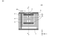
- FIG. 5 is a cross-sectional view parallel to the transport direction of the object to be detected of the magnetic sensor device according to the first embodiment of the present disclosure, and is a cross-sectional view taken along the line II of FIG.
- FIG. 5 is a cross-sectional view of the magnetic sensor device according to the first embodiment as viewed from the insertion / discharge direction of the object to be detected, and is a sectional view taken along line II-II of FIG.
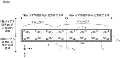
- FIG. 5 is a configuration diagram of an AMR chip according to the first embodiment, and is a layout diagram of a pair of a plurality of magnetoresistive elements.
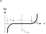
- Circuit diagram of the AMR chip according to the first embodiment Distribution diagram of the magnetic field generated by the magnet according to the first embodiment A graph showing the distribution of the Y-axis bias magnetic field By applied to the magnetoresistive element in FIG.
- FIG. 7 in the Y-axis direction and the strength of the magnetic field applied in the longitudinal direction thereof.
- the transport direction of the object to be detected that is, the lateral direction of the magnetic sensor device
- the longitudinal direction of the magnetic sensor device orthogonal to the transport direction of the object to be detected that is, the reading width direction
- Y the longitudinal direction of the magnetic sensor device orthogonal to the transport direction of the object to be detected
- the axial direction and the direction perpendicular to the XY plane, which is the transport plane, are defined as the Z direction, and are referred to as appropriate.
- FIG. 1 is a ZZ cross-sectional view of the magnetic sensor device 100 according to the first embodiment
- FIG. 2 is a YY cross-sectional view of the magnetic sensor device 100
- FIG. 3 is anisotropic magnetoresistance of the magnetic sensor device 100. It is a top view of the resistance effect element chip
- FIG. 1 corresponds to a cross section taken along line II of FIG. 2
- FIG. 2 corresponds to a cross section taken along line II-II of FIG.
- the magnetic sensor device 100 includes a magnet 1 that generates a bias magnetic field, yokes 2a and 2b that form a magnetic circuit, and an anisotropic magnetic resistance effect element chip that outputs a change in the magnetic field as a change in resistance value. 3, a housing 4 accommodating a magnet 1 and yokes 2a and 2b, a metal shield plate 5 for shielding magnetism, a circuit board 6 for detecting a change in the resistance value of a magnetic resistance effect element, and an output of the circuit board 6.
- a signal processing circuit board 7 for processing the detection signal to be used is provided.
- the magnet 1 includes a rectangular parallelepiped permanent magnet having north and south poles in the Z-axis direction, long in the Y-axis direction and short in the X-axis direction.
- the magnet 1 forms a magnetic field generation unit that applies a bias magnetic field to the anisotropic magnetoresistive element chip 3.
- the yoke 2a and the yoke 2b are each made of a soft magnetic material such as iron in a plate shape.
- the yoke 2a is installed on the upper surface of the magnet 1, and the yoke 2b is installed on the lower surface of the magnet 1.
- the yokes 2a and 2b allow the magnetic flux generated by the magnet 1 to pass through and form a part of the magnetic field generating portion.
- the yokes 2a and 2b are not indispensable, and may be arranged as needed.
- the anisotropic magnetoresistive effect element chip 3 (hereinafter referred to as the AMR chip 3) is arranged on the upper surface of the yoke 2a and outputs the change in the applied magnetic flux as the change in the resistance value. Details of the AMR chip 3 will be described later.
- the housing 4 is made of resin or ceramic and is formed in a box shape with an open upper surface, and houses the magnet 1 and the yokes 2a and 2b.
- the metal shield plate 5 covers and protects the circuit board 6 and the transport path side of the object to be detected 50 of the AMR chip 3.
- the metal shield plate 5 transmits magnetic field lines without being magnetized by itself.
- the circuit board 6 surrounds the AMR chip 3 and is placed on the upper surface of the yoke 2a.
- the circuit board 6 applies a power supply voltage VDD and a ground voltage GND to the AMR chip 3 and outputs a detection signal indicating a change in the resistance of the magnetoresistive sensor.
- the signal processing circuit board 7 is arranged in the lower part of the housing 4, is connected to the circuit board 6 via the cable 8, processes the detection signal, and detects the object to be detected 50.
- the object to be detected 50 is a sheet-shaped object to be detected such as a banknote on which a magnetic material such as magnetic ink is printed.
- the transport direction of the object to be detected 50 is the + X-axis direction.
- the AMR chip 3 has an anisotropic magnetoresistive element 31a arranged line-symmetrically and on a virtual line with a central axis Cx extending in the Y-axis direction, which is the longitudinal direction, passing through the center in the X-axis direction. Eight pairs of 31b are provided.
- the anisotropic magnetoresistive effect elements 31a and 31b each have a long side and a short side in a plan view, and the short side direction is the magnetically sensitive direction and the long side direction is the magnetically insensitive direction.
- the anisotropic magnetoresistive effect elements 31a and 31b are examples of a first resistor and a second resistor.
- the anisotropic magnetoresistive elements 31a and 31b are arranged so that the central axis Cx in the longitudinal direction is at the center position in the X-axis direction of the magnetic field generating member including the magnet 1 and the yokes 2a and 2b.
- the anisotropic magnetoresistive element 31a and the anisotropic magnetoresistive element 31b are arranged line-symmetrically on the central axis Cx in the longitudinal direction.
- the anisotropic magnetoresistive elements 31a and 31b are arranged so that their intervals are expanded or contracted along the Y-axis direction.
- At least two pairs of anisotropic magnetoresistive elements 31a and 31b are arranged line-symmetrically on the central axis Cy in the Y-axis direction of the magnetic field generating member including the magnet 1 and the yokes 2a and 2b.
- the central axis Cy is a central axis extending in the X-axis direction, which is the lateral direction, through the center of the AMR chip 3 in the Y-axis direction.
- the distance between the anisotropic magnetoresistive elements 31a and 31b of the group A including the five sets increases as Y increases.
- the distance between the anisotropic magnetoresistive elements 31a and 31b of the group B including the three sets decreases as Y increases.
- the five sets of the anisotropic magnetic resistance effect elements 31a and 31b belonging to the group A and the three sets of the anisotropic magnetoresistive elements 31a and 31b belonging to the group B are arranged line-symmetrically on the central axis Cx in the Y-axis direction.
- the circuit board 6 applies a power supply voltage VDD to one end of each anisotropic magnetoresistive element 31a.
- a ground voltage GND is applied to one end of each anisotropic magnetoresistive element 31b.
- the other ends of the anisotropic magnetoresistive elements 31a and 31b are short-circuited, and the output of each pair is output to the circuit board 6 via the output signal line.
- the power supply voltage VDD is divided according to the ratio of the resistance values of the anisotropic magnetoresistive elements 31a and 31b, and is output as a detection signal to the output signal line.
- the magnetic fields applied to the anisotropic magnetoresistive elements 31a and 31b change, thereby changing the resistance value and the voltage division ratio. Changes the voltage of the detection signal.
- the circuit board 6 transmits the detection signal to the signal processing circuit board 7, and the signal processing circuit board 7 can detect the object to be detected 50 by processing the detection signal.
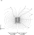
- FIG. 4 is a diagram showing the distribution of magnetic field lines output by the magnetic field generating unit including the magnet 1 and the yokes 2a and 2b. Note that FIG. 4 describes the components necessary for explaining the distribution of the magnetic field lines, and omits the others. As shown in FIG. 4, when viewed in the XZ plane, the magnetic field lines 20 emitted from the north pole of the magnet 1 pass through the yoke 2a and are emitted from the XY and YZ surfaces of the yoke 2a to the outside of the magnet 1 and the yoke 2a. Will be done.
- the central axis in the X-axis direction of the AMR chip 3 that is, the central axis Cx in the longitudinal direction is arranged at the center of the magnet 1 and the yoke 2a in the X-axis direction.
- the central axis in the Y-axis direction orthogonal to the longitudinal direction of the AMR chip 3, that is, the central axis Cy is arranged at the center of the magnet 1 and the yoke 2a in the Y-axis direction. Therefore, the component + Bx in the X-axis direction of the magnetic field indicated by the magnetic field line 20 acts as a bias magnetic field in the X-axis direction of the anisotropic magnetoresistive element 31a.
- the component ⁇ Bx in the ⁇ X-axis direction acts as a bias magnetic field in the X-axis direction of the anisotropic magnetoresistive element 31b.
- This relationship is shown in FIGS. 3A and 4. Due to this bias magnetic field, a magnetic field is stably applied in the longitudinal direction of the anisotropic magnetoresistive elements 31a and 31b. As a result, the hysteresis characteristics of the anisotropic magnetoresistive elements 31a and 31b are suppressed, and a stable output can be obtained.
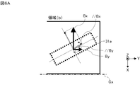
- a magnetic field having an intensity distribution shown in FIG. 5 is applied. That is, in the plan view of FIG. 3A, theoretically, a magnetic field in the + Y axis direction is applied in the area on the + Y side of the central axis Cy, that is, on the right side. Further, in the area on the ⁇ Y side, that is, on the left side of the central axis Cy, a magnetic field in the ⁇ Y axis direction is applied. However, in the central portion, that is, in the range of (a) in FIG. 5, the bias magnetic field By in the Y-axis direction can be regarded as substantially "0".
- the applied magnetic field in the longitudinal direction of the anisotropic magnetoresistive element 31a is the longitudinal component // Bx of the anisotropic magnetoresistive element 31a of the X-axis direction bias magnetic field Bx and the Y-axis direction. It is the sum of the magnetoresistive sensor 31a of the bias magnetic field By and the longitudinal component // By. Therefore, the bias magnetic field in the longitudinal direction of the anisotropic magnetoresistive element 31a is stably supplied from both the X-axis direction bias magnetic field Bx and the Y-axis direction bias magnetic field By.
- the bias magnetic field By in the Y-axis direction faces the ⁇ Y-axis direction.
- the bias magnetic field Bx in the X-axis direction is the same as that in FIG. 6A.
- the applied magnetic field in the longitudinal direction of the anisotropic magnetoresistive sensor 31a is the component // Bx in the longitudinal direction of the anisotropic magnetoresistive element 31a of the X-axis direction bias magnetic field Bx and the Y-axis direction bias magnetic field By.
- the components in the longitudinal direction of the anisotropic magnetoresistive sensor 31a // By are opposite to each other and cancel each other out. Therefore, the difference becomes a bias magnetic field in the longitudinal direction. Therefore, the bias magnetic field in the longitudinal direction of the anisotropic magnetoresistive element 31a becomes small, and the anisotropic magnetoresistive element 31a is easily affected by hysteresis.
- the anisotropy is arranged so that the interval becomes narrower as Y becomes larger.
- the component of the applied magnetic field in the longitudinal direction of the anisotropic magnetic resistance effect element 31a is X.
- the sum of the longitudinal component // Bx of the axially biased magnetic field Bx of the anisotropic magnetic resistance effect element 31a and the longitudinal component // Bx of the anisotropic magnetic resistance effect element 31b of the Y-axis bias magnetic field By. It becomes. Therefore, in the range of (c) in FIG.
- the longitudinal bias magnetic field is stably supplied by the X-axis direction bias magnetic field Bx and the Y-axis direction bias magnetic field By.
- the anisotropic magnetoresistive sensor 31a is formed in the range of the magnet end regardless of whether the direction of the bias magnetic field By in the Y-axis direction is positive or negative.
- the X-axis direction bias magnetic field Bx and the Y-axis direction bias magnetic field By are added to each other with respect to the longitudinal bias magnetic fields of the anisotropic magnetoresistive elements 31a and 31b.
- the sensitivity distribution of the magnetic sensor device 100 of the present embodiment is improved in uniformity, and a more uniform signal distribution can be obtained.
- At least two or more sets of six sets that is, six pairs of anisotropic magnetoresistive element 31a and anisotropic magnetic resistance effect element 31b are line-symmetrical with respect to the central axis Cy.
- the configuration is not limited to this, and at least two or more sets may be configured line-symmetrically with respect to the central axis Cy.
- a total of eight sets of all four sets of the magnetoresistive element 31a and the anisotropic magnetoresistive element 31b existing in the negative region in the Y-axis direction may be line-symmetric with respect to the central axis Cy.
- the bias magnetic field B // in the longitudinal direction of the anisotropic magnetoresistive elements 31a and 31b becomes substantially uniform regardless of the position in the Y-axis direction.
- the sensitivity is also substantially uniform regardless of the position in the Y-axis direction.
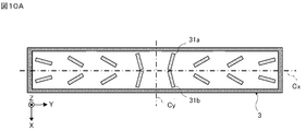
- FIG. 10A is a plan view of the AMR chip 3 of the magnetic sensor 100 according to the third embodiment.
- the position closer to the central axis Cy corresponding to the midpoint in the Y-axis direction, which is the longitudinal direction of the magnetic field generating member including the magnet 1 and the yokes 2a and 2b, is different from the anisotropic magnetoresistive element 31a. It is arranged so that the angle formed by the magnetoresistive effect element 31b is large. However, the sizes of the anisotropic magnetoresistive elements 31a and 31b are the same. In this case, as schematically shown in FIG. 10B, the difference between the positions of the magnetic fields applied to the magnetoresistive element 31a in the Y-axis direction becomes small. Therefore, as shown in FIG. 10C, the uniformity of the sensitivity distribution is improved, and a more uniform signal distribution can be obtained.
- the anisotropic side close to the central axis Cy corresponding to the midpoint in the Y-axis direction which is the longitudinal direction of the magnetic field generating member including the magnet 1 and the yokes 2a and 2b.
- the width W of the magnetoresistive elements 31a and 31b is smaller than the width W of the anisotropic magnetoresistive elements 31a and 31b on the side far from the central axis Cy.
- the magnitude of the Y-axis direction bias magnetic field By is very small on the central axis Cy, but the Y-axis direction bias magnetic field By increases as the distance from the central axis Cy increases, and the anisotropic magnetoresistive element 31a, It affects the sensitivity of 31b and reduces the sensitivity. Therefore, by increasing the width W of the anisotropic magnetoresistive elements 31a and 31b as the distance from the central axis Cy increases, the output values from the anisotropic magnetoresistive elements 31 and 31b are not changed. Consequently, the uniformity of the sensitivity distribution of the magnetic sensor device 100 is improved, and a uniform signal distribution can be obtained.
- the anisotropic magnetoresistive element 31a , 31b that is, the size in the Z-axis direction may be changed according to the position. More specifically, the thickness of the anisotropic magnetoresistive elements 31a and 31b on the side closer to the central axis Cy is larger than the thickness of the anisotropic magnetoresistive elements 31a and 31b on the side farther from the central axis Cy. That is, it has a thick structure.
- the anisotropic magnetoresistive element has a characteristic that the sensitivity increases as the resistance film becomes thinner. Therefore, by adjusting the thickness, the same effect as that of the fourth embodiment can be obtained.
- the portion having the structure shown in the first to fourth embodiments may be limited to only a part of the magnetic sensor device.
- symmetry does not mean strict symmetry.
- the anisotropic magnetoresistive effect elements 31a and 31b have a symmetric deviation at a level capable of functioning as a magnetic sensor with respect to the central axis Cy, and a symmetric deviation based on a manufacturing error.
- the content of the deviation may be any of the size deviation, the position deviation, the angle or orientation deviation, and the like.
- the anisotropic magnetoresistive elements 31a and 31b are drawn as one resistor, but the resistor is as shown in FIG. 10 of Patent No. 6316429 (Patent Document 1). It may have a mianda structure, that is, a folded pattern. Further, the size of the width W of the anisotropic magnetoresistive effect elements 31a and 31b is proportional to the number of times the resistor is folded back. That is, when the width W of the anisotropic magnetoresistive elements 31a and 31b is small, the number of times the resistor is folded back is small, so that the resistance values of the anisotropic magnetoresistive elements 31a and 31b are small and the anisotropic magnetoresistive element is small. When the width W of the 31a and 31b is large, the number of times the resistor is folded back is large, so that the resistance values of the magnetoresistive effect elements 31a and 31b are large.
- the present disclosure can freely combine the embodiments, and each embodiment can be appropriately modified or omitted.
- the resistor constituting the magnetoresistive element an example in which an anisotropic magnetoresistive element is used has been shown, but a GMR (Giant MagnetoResistive Effect) element, a TMR (Tunnel MagnetoResistive Effect), or the like is used. Has the same effect.
- anisotropic magnetoresistive element 31a and the anisotropic magnetoresistive element 31b are arranged line-symmetrically with respect to the central axis Cx in the longitudinal direction of the magnetic field generating portion, it is not necessarily a line object. It does not have to be.
- the device configuration, circuit configuration, etc. are examples and can be changed as appropriate.
Landscapes
- Physics & Mathematics (AREA)
- General Physics & Mathematics (AREA)
- Condensed Matter Physics & Semiconductors (AREA)
- Measuring Magnetic Variables (AREA)
- Hall/Mr Elements (AREA)
Abstract
Description
なお、以下の説明において、被検知物の搬送方向、即ち、磁気センサ装置の短手方向をX軸方向、被検知物の搬送方向に直交する磁気センサ装置の長手方向、即ち読取幅方向をY軸方向、搬送面であるXY面に垂直な方向をZ方向と定義し、適宜参照する。
図1は、実施の形態1に係る磁気センサ装置100の、Z-X断面図、図2は、磁気センサ装置100のY-Z断面図、図3は、磁気センサ装置100の異方性磁気抵抗効果素子チップの上面図であり、図1は、図2のI-I線断面、図2は図1のII-II線断面に相当する。
AMRチップ3は、そのX軸方向の中心を通って長手方向であるY軸方向に伸びる中心軸Cxを挟んで線対称に且つ仮想のライン上に配置された異方性磁気抵抗効果素子31aと31bの対を8対備える。
異方性磁気抵抗効果素子31aと31bは、Y軸方向に沿ってその間隔が拡大又は縮小するように配置されている。また、少なくとも2組の異方性磁気抵抗効果素子31aと31bの対は、磁石1とヨーク2a、2bを含む磁界発生部材のY軸方向の中心軸Cyに線対称に配置されている。中心軸Cyは、AMRチップ3のY軸方向の中心を通って短手方向であるX軸方向に伸びる中心軸である。
このため、磁力線20で示される磁界の、X軸方向の成分+Bxが異方性磁気抵抗効果素子31aのX軸方向バイアス磁界として作用している。反対に異方性磁気抵抗効果素子31b上では、-X軸方向の成分-Bxが異方性磁気抵抗効果素子31bのX軸方向バイアス磁界として作用する。この関係を図3Aおよび図4に示す。このバイアス磁界により、異方性磁気抵抗効果素子31aと31bの長手方向に安定して磁界が印加される。これにより、異方性磁気抵抗効果素子31aと31bのヒステリシス特性が抑制され、安定した出力を得ることができる。
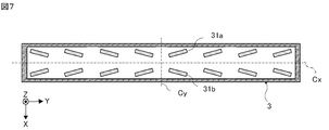
実施の形態1では、少なくとも2組以上である6組、即ち6対の異方性磁気抵抗効果素子31aと異方性磁気抵抗効果素子31bが中心軸Cyに線対称になる構成としている。ただしこの構成に限定されず、少なくとも2組以上が中心軸Cyに線対称に構成されていればよい。例えば、図7に示すように、中心軸CyよりもY軸方向正領域に存在する異方性磁気抵抗効果素子31aと異方性磁気抵抗効果素子31bの4つの組の全てと、中心軸CyよりもY軸方向負領域に存在する磁気抵抗効果素子31aと異方性磁気抵抗効果素子31bの4つの組の全て、計8組を中心軸Cyに対して線対称としてもよい。線対称とすることで、AMRチップ3を複数種類製造する必要がなく、AMRチップ3上に異方性磁気抵抗効果素子31a、31bを形成するための単一のパターン原版を製造するだけで済むため、コスト低減が可能となる。
この場合には、図8に示すように、各異方性磁気抵抗効果素子31a、31bの長手方向のバイアス磁界B//は、Y軸方向の位置によらずほぼ均一となる。また、図9に示すように、感度もY軸方向の位置によらずほぼ均一となる。
実施の形態3に係る磁気センサ装置100について、図10を参照して説明する。なお、図10において、図3Aと同一もしくは同等の構成要素には同一符号を付し、その説明を省略する。
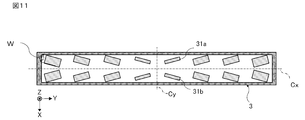
実施の形態4に係る磁気センサ装置について、図11を参照して説明する。
図11において、図3と同一もしくは同等の構成要素には同一符号を付し、その説明を省略する。
図11に示すように異方性磁気抵抗効果素子31a、31bの幅Wを位置に応じて変更する代わりに、或いは、幅Wを位置に応じて変更すると共に、異方性磁気抵抗効果素子31a、31bの厚み、即ち、Z軸方向の大きさを位置に応じて変更するようにしてもよい。より具体的には、中心軸Cyに近い側の異方性磁気抵抗効果素子31a、31bの厚みが、中心軸Cyに遠い側の異方性磁気抵抗効果素子31a、31bの厚みよりも大きい、即ち、厚い構造とする。異方性磁気抵抗効果素子は、抵抗膜が薄い程感度が上がる特性を有する。従って、厚みを調整することにより、実施の形態4と同様の効果を得ることができる。
装置構成、回路構成などは例示であり、適宜変更可能である。
Claims (7)
- 被検知物に交差する磁界を生成する磁界発生部材と、
前記被検知物の搬送方向に直交する方向を長手方向として前記長手方向にライン上に配置された磁気抵抗効果素子と、を備え、
前記磁気抵抗効果素子は、第1の抵抗体と第2の抵抗体とが、前記第1の抵抗体と前記第2の抵抗体との前記搬送方向の間隔の中心が前記磁界発生部材の前記搬送方向における中心位置に位置するように配置された構成を有し、
前記磁界発生部材は、前記第1の抵抗体と前記第2の抵抗体に、前記被検知物の搬送方向の成分と前記長手方向の成分とを有する磁界を印加し、
前記第1の抵抗体と前記第2の抵抗体とは、前記第1の抵抗体と前記第2の抵抗体の一端から前記長手方向の他端に向かうにつれ、前記第1の抵抗体と前記第2の抵抗体の間隔が広がっていく配置であり、
少なくとも2組の前記第1の抵抗体と前記第2の抵抗体が、前記磁界発生部材の前記長手方向に直交する軸に線対称に配置されている、
磁気センサ装置。 - 前記第1の抵抗体と前記第2の抵抗体の組が、前記磁界発生部材の前記長手方向に直交する短手方向の中心を通り前記長手方向に沿った軸に線対称に配置されている、
請求項1に記載の磁気センサ装置。 - 前記第1の抵抗体と前記第2の抵抗体の対で構成される前記磁気抵抗効果素子の組は、全ての組が前記磁界発生部材の前記長手方向の中心で該長手方向に直交する軸である中心軸に線対称に配置されている、
請求項1又は2に記載の磁気センサ装置。 - 前記磁界発生部材の前記長手方向に延在する前記第1の抵抗体と前記第2の抵抗体は、前記磁界発生部材の前記長手方向の中心軸に近い側の前記第1の抵抗体と前記第2の抵抗体が前記中心軸となす角度が、前記中心軸に遠い側の前記第1の抵抗体と前記第2の抵抗体が前記中心軸となす角度以下になるように配置されている、
請求項1から3の何れか1項に記載の磁気センサ装置。 - 前記磁界発生部材の前記長手方向に延在する前記第1の抵抗体と前記第2の抵抗体は、前記磁界発生部材の前記長手方向の中心軸に近い側の前記第1の抵抗体と前記第2の抵抗体の幅が、前記中心軸に遠い側の前記第1の抵抗体と前記第2の抵抗体の幅よりも小さくなるように配置されている、請求項1から4の何れか1項に記載の磁気センサ装置。
- 前記磁界発生部材の前記長手方向に延在する前記第1の抵抗体と前記第2の抵抗体は、前記磁界発生部材の前記長手方向の中心軸に近い側の前記第1の抵抗体と前記第2の抵抗体の厚みが、前記中心軸に遠い側の前記第1の抵抗体と前記第2の抵抗体の厚みよりも厚くなるように配置されている、請求項1から5の何れか1項に記載の磁気センサ装置。
- 前記磁界発生部材は、その前記長手方向の中心軸を基準に、反対方向の磁界を前記第1の抵抗体と前記第2の抵抗体に印加する、
請求項1から6の何れか1項に記載の磁気センサ装置。
Priority Applications (4)
| Application Number | Priority Date | Filing Date | Title |
|---|---|---|---|
| JP2021537664A JP6964830B2 (ja) | 2019-08-06 | 2020-07-17 | 磁気センサ装置 |
| CN202080052930.5A CN114207857B (zh) | 2019-08-06 | 2020-07-17 | 磁传感器装置 |
| DE112020003798.3T DE112020003798B4 (de) | 2019-08-06 | 2020-07-17 | Magnetische Sensorvorrichtung |
| US17/625,774 US12306273B2 (en) | 2019-08-06 | 2020-07-17 | Magnetic sensor device |
Applications Claiming Priority (2)
| Application Number | Priority Date | Filing Date | Title |
|---|---|---|---|
| JP2019-144767 | 2019-08-06 | ||
| JP2019144767 | 2019-08-06 |
Publications (1)
| Publication Number | Publication Date |
|---|---|
| WO2021024758A1 true WO2021024758A1 (ja) | 2021-02-11 |
Family
ID=74504080
Family Applications (1)
| Application Number | Title | Priority Date | Filing Date |
|---|---|---|---|
| PCT/JP2020/027823 Ceased WO2021024758A1 (ja) | 2019-08-06 | 2020-07-17 | 磁気センサ装置 |
Country Status (5)
| Country | Link |
|---|---|
| US (1) | US12306273B2 (ja) |
| JP (1) | JP6964830B2 (ja) |
| CN (1) | CN114207857B (ja) |
| DE (1) | DE112020003798B4 (ja) |
| WO (1) | WO2021024758A1 (ja) |
Citations (4)
| Publication number | Priority date | Publication date | Assignee | Title |
|---|---|---|---|---|
| JPS63908B2 (ja) * | 1985-04-15 | 1988-01-09 | Daikin Kogyo Co Ltd | |
| JPS6316429B2 (ja) * | 1983-03-24 | 1988-04-08 | Toyo Rubber Ind Co | |
| JP3105238U (ja) * | 2004-05-14 | 2004-10-21 | ニッコーシ株式会社 | 磁気センサー装置 |
| WO2014156793A1 (ja) * | 2013-03-26 | 2014-10-02 | 浜松光電株式会社 | 磁性体検出装置 |
Family Cites Families (9)
| Publication number | Priority date | Publication date | Assignee | Title |
|---|---|---|---|---|
| JPH10170619A (ja) * | 1996-12-06 | 1998-06-26 | Fujitsu Takamizawa Component Kk | 磁気センサとその交番バイアス磁界印加方法 |
| DE10342260B4 (de) | 2003-09-11 | 2014-11-20 | Meas Deutschland Gmbh | Magnetoresistiver Sensor in Form einer Halb- oder Vollbrückenschaltung |
| CN103038659B (zh) * | 2010-07-30 | 2015-07-08 | 三菱电机株式会社 | 磁性体检测装置 |
| DE112015002254B4 (de) | 2014-05-13 | 2025-04-10 | Mitsubishi Electric Corporation | Magnetsensorvorrichtung |
| CN106560005B (zh) * | 2014-06-11 | 2019-09-06 | 三菱电机株式会社 | 磁性传感器装置 |
| US10353021B2 (en) * | 2014-07-25 | 2019-07-16 | Mitsubishi Electric Corporation | Magnetic sensor device |
| WO2017191823A1 (ja) * | 2016-05-06 | 2017-11-09 | 三菱電機株式会社 | 磁気センサ装置 |
| JP2018048832A (ja) * | 2016-09-20 | 2018-03-29 | 株式会社東芝 | 磁気センサ、磁気センサ装置、診断装置 |
| JP7040104B2 (ja) | 2018-02-19 | 2022-03-23 | 富士通株式会社 | 学習プログラム、学習方法および学習装置 |
-
2020
- 2020-07-17 JP JP2021537664A patent/JP6964830B2/ja active Active
- 2020-07-17 DE DE112020003798.3T patent/DE112020003798B4/de active Active
- 2020-07-17 US US17/625,774 patent/US12306273B2/en active Active
- 2020-07-17 WO PCT/JP2020/027823 patent/WO2021024758A1/ja not_active Ceased
- 2020-07-17 CN CN202080052930.5A patent/CN114207857B/zh active Active
Patent Citations (4)
| Publication number | Priority date | Publication date | Assignee | Title |
|---|---|---|---|---|
| JPS6316429B2 (ja) * | 1983-03-24 | 1988-04-08 | Toyo Rubber Ind Co | |
| JPS63908B2 (ja) * | 1985-04-15 | 1988-01-09 | Daikin Kogyo Co Ltd | |
| JP3105238U (ja) * | 2004-05-14 | 2004-10-21 | ニッコーシ株式会社 | 磁気センサー装置 |
| WO2014156793A1 (ja) * | 2013-03-26 | 2014-10-02 | 浜松光電株式会社 | 磁性体検出装置 |
Also Published As
| Publication number | Publication date |
|---|---|
| DE112020003798T5 (de) | 2022-05-25 |
| US12306273B2 (en) | 2025-05-20 |
| CN114207857B (zh) | 2025-08-12 |
| US20220244327A1 (en) | 2022-08-04 |
| DE112020003798B4 (de) | 2026-02-26 |
| JPWO2021024758A1 (ja) | 2021-11-25 |
| JP6964830B2 (ja) | 2021-11-10 |
| CN114207857A (zh) | 2022-03-18 |
Similar Documents
| Publication | Publication Date | Title |
|---|---|---|
| JP5867235B2 (ja) | 磁気センサ装置 | |
| US7126327B1 (en) | Asymmetrical AMR wheatstone bridge layout for position sensor | |
| EP2520945B1 (en) | Magnetic field detecting apparatus and current sensor | |
| CN104204835B (zh) | 磁性传感器装置 | |
| JP6300908B2 (ja) | 磁気センサ装置 | |
| CN110235012B (zh) | 磁阻效应元件单元及磁阻效应元件装置 | |
| CN105026924A (zh) | 磁特性检测装置 | |
| CN106537166B (zh) | 磁性传感器装置 | |
| JPH054307U (ja) | 磁気センサ | |
| CN105190339A (zh) | 磁性体检测装置 | |
| US11614500B2 (en) | Integrated magnetometer and method of detecting a magnetic field | |
| US10352682B2 (en) | Displacement detection device | |
| CN108156821A (zh) | 磁传感器装置 | |
| JP5799882B2 (ja) | 磁気センサ装置 | |
| JP6964830B2 (ja) | 磁気センサ装置 | |
| JP6980166B1 (ja) | 磁気センサ装置 | |
| WO2017126373A1 (ja) | 磁気媒体検出装置 | |
| WO2017199787A1 (ja) | 磁気センサ | |
| KR20230089608A (ko) | 3축 자기저항 센서 |
Legal Events
| Date | Code | Title | Description |
|---|---|---|---|
| 121 | Ep: the epo has been informed by wipo that ep was designated in this application |
Ref document number: 20849134 Country of ref document: EP Kind code of ref document: A1 |
|
| ENP | Entry into the national phase |
Ref document number: 2021537664 Country of ref document: JP Kind code of ref document: A |
|
| WWE | Wipo information: entry into national phase |
Ref document number: 112020003798 Country of ref document: DE |
|
| 122 | Ep: pct application non-entry in european phase |
Ref document number: 20849134 Country of ref document: EP Kind code of ref document: A1 |
|
| WWG | Wipo information: grant in national office |
Ref document number: 17625774 Country of ref document: US |
|
| WWG | Wipo information: grant in national office |
Ref document number: 202080052930.5 Country of ref document: CN |
|
| WWG | Wipo information: grant in national office |
Ref document number: 112020003798 Country of ref document: DE |