WO2021024600A1 - 表示装置 - Google Patents
表示装置 Download PDFInfo
- Publication number
- WO2021024600A1 WO2021024600A1 PCT/JP2020/022224 JP2020022224W WO2021024600A1 WO 2021024600 A1 WO2021024600 A1 WO 2021024600A1 JP 2020022224 W JP2020022224 W JP 2020022224W WO 2021024600 A1 WO2021024600 A1 WO 2021024600A1
- Authority
- WO
- WIPO (PCT)
- Prior art keywords
- display
- image
- pixels
- light
- display device
- Prior art date
- Legal status (The legal status is an assumption and is not a legal conclusion. Google has not performed a legal analysis and makes no representation as to the accuracy of the status listed.)
- Ceased
Links
Images


Classifications
-
- G—PHYSICS
- G02—OPTICS
- G02B—OPTICAL ELEMENTS, SYSTEMS OR APPARATUS
- G02B30/00—Optical systems or apparatus for producing three-dimensional [3D] effects, e.g. stereoscopic images
- G02B30/10—Optical systems or apparatus for producing three-dimensional [3D] effects, e.g. stereoscopic images using integral imaging methods
-
- H—ELECTRICITY
- H04—ELECTRIC COMMUNICATION TECHNIQUE
- H04N—PICTORIAL COMMUNICATION, e.g. TELEVISION
- H04N13/00—Stereoscopic video systems; Multi-view video systems; Details thereof
- H04N13/30—Image reproducers
- H04N13/302—Image reproducers for viewing without the aid of special glasses, i.e. using autostereoscopic displays
- H04N13/31—Image reproducers for viewing without the aid of special glasses, i.e. using autostereoscopic displays using parallax barriers
-
- G—PHYSICS
- G02—OPTICS
- G02B—OPTICAL ELEMENTS, SYSTEMS OR APPARATUS
- G02B3/00—Simple or compound lenses
- G02B3/0006—Arrays
- G02B3/0037—Arrays characterized by the distribution or form of lenses
- G02B3/0056—Arrays characterized by the distribution or form of lenses arranged along two different directions in a plane, e.g. honeycomb arrangement of lenses
-
- G—PHYSICS
- G02—OPTICS
- G02B—OPTICAL ELEMENTS, SYSTEMS OR APPARATUS
- G02B30/00—Optical systems or apparatus for producing three-dimensional [3D] effects, e.g. stereoscopic images
- G02B30/20—Optical systems or apparatus for producing three-dimensional [3D] effects, e.g. stereoscopic images by providing first and second parallax images to an observer's left and right eyes
- G02B30/26—Optical systems or apparatus for producing three-dimensional [3D] effects, e.g. stereoscopic images by providing first and second parallax images to an observer's left and right eyes of the autostereoscopic type
- G02B30/30—Optical systems or apparatus for producing three-dimensional [3D] effects, e.g. stereoscopic images by providing first and second parallax images to an observer's left and right eyes of the autostereoscopic type involving parallax barriers
-
- G—PHYSICS
- G02—OPTICS
- G02B—OPTICAL ELEMENTS, SYSTEMS OR APPARATUS
- G02B30/00—Optical systems or apparatus for producing three-dimensional [3D] effects, e.g. stereoscopic images
- G02B30/20—Optical systems or apparatus for producing three-dimensional [3D] effects, e.g. stereoscopic images by providing first and second parallax images to an observer's left and right eyes
- G02B30/26—Optical systems or apparatus for producing three-dimensional [3D] effects, e.g. stereoscopic images by providing first and second parallax images to an observer's left and right eyes of the autostereoscopic type
- G02B30/33—Optical systems or apparatus for producing three-dimensional [3D] effects, e.g. stereoscopic images by providing first and second parallax images to an observer's left and right eyes of the autostereoscopic type involving directional light or back-light sources
-
- G—PHYSICS
- G03—PHOTOGRAPHY; CINEMATOGRAPHY; ANALOGOUS TECHNIQUES USING WAVES OTHER THAN OPTICAL WAVES; ELECTROGRAPHY; HOLOGRAPHY
- G03B—APPARATUS OR ARRANGEMENTS FOR TAKING PHOTOGRAPHS OR FOR PROJECTING OR VIEWING THEM; APPARATUS OR ARRANGEMENTS EMPLOYING ANALOGOUS TECHNIQUES USING WAVES OTHER THAN OPTICAL WAVES; ACCESSORIES THEREFOR
- G03B35/00—Stereoscopic photography
- G03B35/18—Stereoscopic photography by simultaneous viewing
- G03B35/24—Stereoscopic photography by simultaneous viewing using apertured or refractive resolving means on screens or between screen and eye
-
- H—ELECTRICITY
- H04—ELECTRIC COMMUNICATION TECHNIQUE
- H04N—PICTORIAL COMMUNICATION, e.g. TELEVISION
- H04N13/00—Stereoscopic video systems; Multi-view video systems; Details thereof
- H04N13/30—Image reproducers
- H04N13/302—Image reproducers for viewing without the aid of special glasses, i.e. using autostereoscopic displays
-
- H—ELECTRICITY
- H04—ELECTRIC COMMUNICATION TECHNIQUE
- H04N—PICTORIAL COMMUNICATION, e.g. TELEVISION
- H04N13/00—Stereoscopic video systems; Multi-view video systems; Details thereof
- H04N13/30—Image reproducers
- H04N13/324—Colour aspects
-
- H—ELECTRICITY
- H04—ELECTRIC COMMUNICATION TECHNIQUE
- H04N—PICTORIAL COMMUNICATION, e.g. TELEVISION
- H04N13/00—Stereoscopic video systems; Multi-view video systems; Details thereof
- H04N13/30—Image reproducers
- H04N13/349—Multi-view displays for displaying three or more geometrical viewpoints without viewer tracking
- H04N13/351—Multi-view displays for displaying three or more geometrical viewpoints without viewer tracking for displaying simultaneously
-
- H—ELECTRICITY
- H04—ELECTRIC COMMUNICATION TECHNIQUE
- H04N—PICTORIAL COMMUNICATION, e.g. TELEVISION
- H04N13/00—Stereoscopic video systems; Multi-view video systems; Details thereof
- H04N13/30—Image reproducers
- H04N13/356—Image reproducers having separate monoscopic and stereoscopic modes
-
- H—ELECTRICITY
- H04—ELECTRIC COMMUNICATION TECHNIQUE
- H04N—PICTORIAL COMMUNICATION, e.g. TELEVISION
- H04N13/00—Stereoscopic video systems; Multi-view video systems; Details thereof
- H04N13/30—Image reproducers
- H04N13/361—Reproducing mixed stereoscopic images; Reproducing mixed monoscopic and stereoscopic images, e.g. a stereoscopic image overlay window on a monoscopic image background
Definitions
- This disclosure relates to a display device.
- Patent Document 1 discloses a decorative layer, a light display element, and a multi-functional luminance difference decorative screen including a control device for controlling the light display element.
- the decorative layer is provided in front of the light display element and is a translucent pattern, the light display element is a light source, is connected to a control device, and behind the decoration layer is content to be displayed. ..
- the decorative screen not only displays the content behind the decorative layer, but also functions as a decoration. With this configuration, while the structure is simple and the use is wide-ranging, it has a dual use of decoration and content display, and it is possible to efficiently use the space.
- An object of the present disclosure is to provide a display device capable of recognizablely reproducing an image having an appropriate texture by an observer by combining an image provided on a display surface and an image by a light field display.
- a plurality of display devices are arranged on a side opposite to the outer surface of a first display unit that displays a non-directional display image that is invariant regardless of the viewing direction of the observer and the outer surface of the first display unit.
- the pixels are arranged in two dimensions, and the second display unit that displays a display image having different directions depending on the viewing direction of the observer, the outer surface of the first display unit, and the second display unit.
- An optical element array arranged in parallel with the light emitting surface of the second display unit, in which each of the plurality of optical elements is arranged corresponding to a predetermined unit of pixels among the plurality of pixels, and the second A drive unit for lighting a predetermined pixel among the plurality of pixels of the display unit is provided.
- an image provided on a display surface and an image produced by a light field display can be combined so that an observer can recognize an image having an appropriate texture.
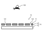
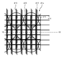
- FIG. 1 Top view showing the outer surface of the display device according to the first embodiment.
- the block diagram which shows the structure of the drive part of the display device which concerns on Embodiment 1.
- a block diagram showing a configuration of a drive unit of the display device according to the second embodiment A block diagram showing a specific example of the configuration of the drive unit of the display device according to the second embodiment.
- a decorative screen has been proposed in which a light source and content are provided behind the decorative layer to provide decoration by the decorative layer and information on the content to be displayed by light.
- this kind of conventional decorative screen there is a problem that the information of the content cannot be changed because only the fixed decoration and the content are displayed. Further, in the case of the configuration in which the content is displayed by the pinhole and the light source, it is difficult to display the fine content.
- the content to be displayed is only displayed at the same position as the decorative surface of the decorative layer, and there is a problem that three-dimensional content cannot be displayed. It was not possible to express textures such as brilliance that differ depending on the viewing direction of the observer.
- a light field display capable of reproducing a stereoscopic image is applied to a display device having a display surface such as a decorative layer.
- a display surface such as a decorative layer.
- FIG. 1 is a plan view showing the outer surface of the display device according to the first embodiment.
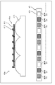
- FIG. 2 is a diagram schematically showing a configuration of a display unit of the display device according to the first embodiment.
- FIG. 2 schematically shows a 2-2 cross section of FIG. 1, that is, a cross section in the thickness direction (emission light direction) of the display device.
- the display device 10 includes a decorative layer 11, a pinhole film 12, and a display 13 in this order from the outer surface side (the side from which light is emitted).
- the decorative layer 11 as an example of the first display unit has a non-directional display surface that is invariant regardless of the viewing direction of the observer.
- the decorative layer 11 is a plate member having various decorations on the outer surface as a non-directional display surface, such as an image of a painting or a photograph or a printed matter, decoration by unevenness, texture of cloth or the like, plating, etc. It is composed of a flat member such as a membrane member.
- the display 13 as an example of the second display unit displays an image having different directions depending on the viewing direction of the observer.
- the display 13 is composed of a self-luminous display device such as an organic EL (Electroluminescence) display, an inorganic EL display, an LED (Light Emission Diode) display, a plasma display, and a cathode ray tube.
- a self-luminous display device such as an organic EL (Electroluminescence) display, an inorganic EL display, an LED (Light Emission Diode) display, a plasma display, and a cathode ray tube.
- a plurality of pixels are arranged in two dimensions in the vertical and horizontal directions on the display surface (light emitting surface, upper surface of FIG. 2) on the decorative layer 11 side, and each pixel in the matrix shape is turned on and off to create an image. Is displayed.
- the display 13 may be configured by a liquid crystal display (LCD: liquid Crystal Display) in which a self-luminous display device is formed by
- a pinhole film 12 as an example of the optical element array is provided on the surface (lower surface of FIG. 2) of the decorative layer 11 on the display 13 side.
- the optical element array is arranged between the outer surface of the decorative layer 11 and the display 13 in parallel with the light emitting surface of the display 13.
- one optical element corresponds to a pixel of a predetermined unit of the display 13, and a plurality of optical elements are arranged two-dimensionally at predetermined intervals.
- the pinhole film 12 has a pinhole array 122 in which pinholes 121 are arranged and formed as a plurality of optical elements in two dimensions in the vertical and horizontal directions at predetermined intervals on the film surface. As shown in FIG. 1, the pinhole 121 is formed so as to penetrate the outer surface of the decorative layer 11, and the decorative layer 11 also has the pinhole array 122. Of the light emitted from the display 13, the pinhole film 12 transmits only the emitted light that passes through each pinhole 121 of the pinhole array 122 and emits the light to the outside of the decorative layer 11.
- the pinhole array 122 is provided with one pinhole 121 corresponding to a plurality of pixels for each pixel of a predetermined unit of the display 13.
- the light field display 15 is composed of the display 13 and the pinhole film 12.
- the image by the light field display 15 is reproduced in the space on the front side (observer side) of the decorative layer 11 when viewed from the observer's viewpoint 105, and the brightness, wavelength, etc. are reproduced depending on the viewing direction.
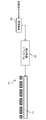
- FIG. 3 is a block diagram showing a configuration of a drive unit of the display device according to the first embodiment.
- a display drive circuit 60 is connected to the display 13 of the display device 10 as an example of a drive unit, and the display drive circuit 60 is connected to the control device 90.
- the control device 90 performs drive control of the display drive circuit 60 based on an external signal from the outside or a display control signal output by the control device 90 itself.
- the display drive circuit 60 supplies a drive signal to the display 13 based on the display control signal from the control device 90.
- the display 13 is controlled by a drive signal from the display drive circuit 60, such as display mode of the display, for example, display / non-display of an image, lighting / extinguishing of each pixel, lighting mode, and the like.
- the operation of the light field display 15 in the display device 10 of the first embodiment that is, the display of an image by the light field display will be described.
- FIG. 4 is a diagram showing an example of the emitted luminous flux in the display device of the first embodiment.
- FIG. 4 describes the direction of the emitted luminous flux due to the lighting of the pixel at a predetermined position.
- the plurality of pixels 131 of the display 13 and the pinhole 121 of the pinhole film 12 are arranged at a predetermined distance.
- a light flux that diffuses slightly according to the width of the pixel and the width of the pinhole is emitted to the decorative layer 11 side, becomes a light flux toward a predetermined direction, and irradiates the space on the observer side. Will be done.
- the luminous flux 135C emitted from the pixel C passes through the pinhole and is emitted in the diagonally upward left direction of FIG. 4, and the luminous flux 135D emitted from the pixel D passes through the pinhole and is FIG. It is emitted diagonally upward to the right.
- the direction of the emitted luminous flux can be controlled by lighting the pixel at a predetermined position.
- the arrangement of the pixels 131 of the display 13 is shown in one dimension in FIG. 4, the pixels 131 are similarly arranged in the direction perpendicular to the paper surface, and the pixels 131 are arranged in two dimensions. Therefore, the light field display 15 using the display 13 and the pinhole film 12 can irradiate the light field display 15 by controlling the emission direction of the light flux in any direction from the surface of the pinhole film 12 in all directions of the hemisphere.
- FIG. 5 is a diagram illustrating texture display by the display device of the first embodiment.
- the emission direction of the light flux passing through the pinhole 121 differs depending on the position of the lit pixel.
- RGB pixels are arranged in order, for example, pixels R1, G1, B1, ... Rn, Gn, Bn, ....
- the emission luminous fluxes R1, G1, and B1 when the pixel R1 that emits red R light, the pixel G1 that emits green G light, and the pixel B1 that emits blue B light are turned on are pins. It passes through the hole 121 and is emitted diagonally upward to the right in FIG.
- the emitted luminous fluxes R3, G3, and B3 when the pixels R3, the pixels G3, and the pixels B3 are turned on pass through the pinhole 121 and are emitted in the diagonally upward left direction in FIG. Therefore, for example, when the pixel R1 is lit for the red R and the pixel B3 is lit for the blue B, when the observer sees from the right direction of FIG. 5, a strong red light is observed, and the light is seen from the left direction of FIG. A strong blue light is observed. The same applies to other pixels. Further, when the brightness of the pixel to be lit differs depending on the pixel position, the brightness of the luminous flux changes depending on the emission direction.
- FIG. 6 is a diagram showing an example of reproducing colors different depending on the direction as an example of texture display in the display device of the first embodiment.
- pixels R1, ... Rn are lit for red R
- pixels G2, ... G (n + 1) are lit for green G
- pixels B3, ... B (n + 2) are lit for blue B.
- hatched or white pixels represent lit pixels
- black pixels represent extinguished pixels (non-lit pixels).
- the red emission luminous flux R1, ... Rn is emitted diagonally upward to the right in FIG. 6
- the green emission luminous flux G2, ... G (n + 1) is emitted in the upward direction in FIG. 6
- the blue emission luminous flux B3, ... B (n + 2) is emitted diagonally upward to the left in FIG.
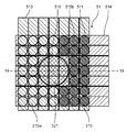
- FIG. 7 is a diagram showing an example of reproducing the texture display of a stereoscopic image by the display device of the first embodiment.
- FIG. 7 describes the reproduction of a stereoscopic image by lighting the pixels at a plurality of positions.
- the display device 10 by lighting a plurality of pixels at predetermined positions, an image is reproduced at an intersection of a plurality of emitted luminous fluxes.
- the light fluxes 135D1, 135D2, 135D3 irradiated in a predetermined direction from the plurality of pixels D1, the pixels D2, and the pixels D3, respectively, intersect at the intersection D, and an image emitting light from the intersection D is formed.
- the pixels 131 are arranged two-dimensionally as in the example of FIG. 4, the light field display 15 by the display 13 and the pinhole film 12 is at an arbitrary position in all directions of the hemisphere from the surface of the pinhole film 12. It is possible to reproduce a three-dimensional image. Examples of reproduction of texture display by a three-dimensional image include a texture such as cloth, wallpaper, a painting such as an oil painting, a pattern on a printed matter, or a feeling of unevenness on the surface of an image. It is also possible to reproduce both the effect of the texture of light rays whose color and brightness change depending on the viewing direction of the observer and the effect of the texture of surface irregularities due to the stereoscopic image.
- a light beam emitted from an object to be reproduced (specifically, a vector wave transmitted through the object or a vector wave reflected by the object) is detected by a sensor such as a camera and stored as image data. Then, the stored light rays are tracked in the direction opposite to the sensor, and the brightness distribution and the wavelength distribution when the light rays are incident on the display surface through the pinhole array 122 in the direction from the object toward the display 13 are calculated. Based on this luminance distribution and wavelength distribution, it is determined whether each pixel on the display 13 is turned on or off, and display data of the original image for reproducing the displayed image is generated and stored.
- a drive signal is supplied from the display drive circuit 60 based on the display data of the original image, and the pixels at the predetermined positions of the display 13 are turned on.
- the light beam emitted from the display 13 through the pinhole array 122 in a predetermined direction is reproduced, and is seen by the observer as an image having the texture of the target object.
- the size of one pixel of the display 13 is smaller than the distance between the plurality of pinholes 121 of the pinhole array 122.
- the resolution of the light field display is determined by the distance between optical elements such as pinholes in the optical element array or the outer diameter of the optical element such as a lens, and it is difficult to reproduce a high resolution image only with the light field display.
- the resolution of the light-field display can be supplemented, and a high-resolution and textured image can be reproduced.
- a decorative surface made of a decorative layer and a display and a light field display made of a pinhole film are arranged so as to form a display device.
- the image decorated by the decorative layer and the display image expressing the texture of the light field display can be superimposed and projected, and in addition to the high-definition image on the display surface of the decorative layer, the image can be projected. Images with different textures can be recognized and reproduced depending on the observation direction of the light field display.
- FIG. 8 is a diagram schematically showing a configuration of a display unit of the display device according to the second embodiment.
- FIG. 8 schematically shows a cross section of the display device in the thickness direction (emission light direction).
- the second embodiment is an example in which a display is provided in place of the decorative layer of the first embodiment as the first display unit on the outer surface side of the display device.
- the components different from those of the first embodiment will be mainly described, and duplicate description will be omitted.
- the display device 30 includes a first display 31 and a second display 33 in order from the outer surface side (the side from which light is emitted).
- the first display 31 as an example of the first display unit is composed of, for example, a self-luminous display device such as an organic EL display, a reflective display device such as electronic paper, or the like.
- a plurality of pixels are arranged two-dimensionally in the vertical and horizontal directions on the display surface (light emitting surface, upper surface of FIG. 8) on the outer front side, and the image is displayed by displaying and hiding each pixel in the matrix shape. Is displayed.
- the second display 33 as an example of the second display unit is a self-luminous display device such as an organic EL display, an inorganic EL display, an LED display, a plasma display, a cathode line tube, or a liquid crystal display, as in the first embodiment. It is composed of a liquid crystal display in which a self-luminous display device is formed by a display panel and a backlight.
- the first display 31 has a pinhole array 322 as an example of the optical element array.
- the first display 31 has a light-transmitting portion that transmits light from the back side to the outer surface on the front side of the display surface, and pinholes 321 by the light-transmitting portion are arranged and formed in two dimensions vertically and horizontally at predetermined intervals.
- a pinhole array 322 having a plurality of pinholes 321 is configured.
- the first display 31 transmits only the emitted light passing through each pinhole 321 of the pinhole array 322 and emits the emitted light to the outside of the first display 31.
- the pinhole array 322 is provided with one pinhole 321 corresponding to a plurality of pixels for each pixel of a predetermined unit of the second display 33.
- the light field display 35 is composed of the second display 33 and the pinhole array 322 of the first display 31.
- FIG. 9 is a block diagram showing a configuration of a drive unit of the display device according to the second embodiment.
- a first display drive circuit 61 is connected to the first display 31 of the display device 30 as an example of a drive unit, a second display drive circuit 63 is connected to the second display 33, and the first display drive circuit 61 is connected. And the second display drive circuit 63 is connected to the control device 90.
- the control device 90 performs drive control of the first display drive circuit 61 and the second display drive circuit 63 based on an external signal from the outside or a display control signal output by the control device 90 itself.
- the first display drive circuit 61 supplies a drive signal to the first display 31 based on the display control signal from the control device 90.
- the second display drive circuit 63 supplies a drive signal to the second display 33 based on the display control signal from the control device 90.
- the display mode of the display for example, display / non-display of an image, switching of a display image, and the like are controlled by a drive signal from the first display drive circuit 61.
- the display mode of the display for example, display / non-display of an image, lighting / extinguishing of each pixel, lighting mode, etc., is controlled by a drive signal from the second display drive circuit 63.
- the first display 31 displays an image that is invariant depending on the viewing direction from the viewpoint of the observer, that is, an image that does not depend on the orientation of the observer on the display surface.
- the second display 33 displays an image that differs depending on the viewing direction from the viewpoint of the observer, that is, an image that depends on the orientation of the observer.
- a common image that does not depend on the orientation is displayed on the first display 31 when viewed from the observer, and the second display 33 is displayed in the space in front of the first display 31 (observer side).
- An image depending on the orientation using the light field display 35 is reproduced.
- FIG. 10 is a block diagram showing a specific example of the configuration of the drive unit of the display device according to the second embodiment.
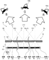
- a light source direction / wavelength characteristic identification device 210 for detecting the direction and wavelength characteristics of the light source is connected to the control device 90.
- the light source direction / light source wavelength characteristic identification device 210 is configured to include a photodetector such as a camera, an optical sensor, and an image sensor, and detects a light source that irradiates a target object reproduced by the display device 30 with light.
- the light source direction / light source wavelength characteristic identification device 210 is composed of, for example, one or a plurality of 360-degree cameras, and extracts a high-luminance portion from images in each direction obtained by the 360-degree cameras by image processing to determine the direction of the light source. Is calculated.
- the light source direction / wavelength characteristic identification device 210 includes information on the direction and wavelength characteristics of the light source at the sensor position of the identification device (light source direction / wavelength characteristic information 221) and position information of the sensor of the identification device (sensor position) as light source information.
- the control device 90 includes a light source direction calculation circuit 91, a display object data storage unit 92, a ray tracing calculation circuit 93, a common image discrimination calculation circuit 94, a non-directional image drawing calculation circuit 95, and a directional image drawing calculation circuit 96.
- the control device 90 inputs light source information from the light source direction / light source wavelength characteristic identification device 210.
- the light source direction calculation circuit 91 calculates the direction and wavelength characteristics of the light source at the display position based on the light source direction / wavelength characteristic information 221 at the sensor position and the sensor position coordinates 222, and uses this calculation result as the light source data at the display position. Output.
- the display object data storage unit 92 stores the shape data 921 of the display object to be reproduced and the object surface characteristic data 922 such as the reflection characteristic of the display object as the display object data.
- the ray tracing calculation circuit 93 inputs the display object data from the display object data storage unit 92 and the light source data at the display position from the light source direction calculation circuit 91.
- the ray tracing calculation circuit 93 performs rendering processing by the ray tracing method based on the shape data 921 of the display object, the object surface characteristic data 922, and the direction and wavelength characteristic information of the light source at the display position.
- the ray tracing calculation circuit 93 calculates ray characteristic data such as brightness and chromaticity of light in each direction for a display object illuminated by a light source by a ray tracing method.
- the common image discrimination calculation circuit 94 is based on the calculated light ray characteristic data such as brightness and chromaticity of light in each direction, and is oriented-independent non-directional ray characteristic data and direction-dependent ray characteristic data. Discriminate to. That is, the common image discrimination calculation circuit 94 separates the directional components with respect to the light characteristics such as the brightness and chromaticity of the detected light.
- the non-directional image drawing calculation circuit 95 calculates a first display control signal for drawing a display image independent of the orientation of the display object to be reproduced from the discriminated non-directional light characteristic data.
- the directional image drawing calculation circuit 96 calculates a second display control signal for drawing a display image depending on the orientation of the display object to be reproduced from the discriminated directional ray characteristic data.
- FIG. 11 and 12 are diagrams for explaining an example of arithmetic processing for discriminating between non-directional ray characteristic data that does not depend on the direction and directional ray characteristic data that depends on the direction.
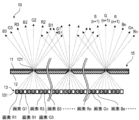
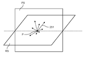
- FIG. 11 is a diagram schematically showing light rays emitted from an arbitrary point P in various directions, and as an example of the brightness distribution in each direction from the point P, is a plane direction (on a plane) of a predetermined plane PS. The angular distribution of the brightness in the 360 ° all-around direction) is shown.
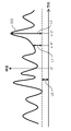
- FIG. 12 is a characteristic diagram showing the brightness distribution of the light rays in FIG. 11 for each direction.
- the reference plane RS corresponds to, for example, the display plane of the display
- the plane PS is a plane that intersects the reference plane RS perpendicularly.
- the light beam 251 emitted from a predetermined point P on the display object is emitted in various directions and has a luminance distribution according to the direction.
- the common image discrimination calculation circuit 94 calculates the brightness distribution for each direction on the plane PS perpendicular to the reference plane RS based on the ray characteristic data having the brightness and chromaticity information of the light in each direction.
- FIG. 12 it is assumed that the luminance distribution 252 for each direction at each angle such as ⁇ 1 °, ⁇ 2 °, ..., Etc. has been calculated.
- the minimum brightness of the light rays in all directions is defined as the brightness LO that does not depend on the direction, and the value obtained by subtracting the brightness LO that does not depend on the direction from the brightness in each direction is defined as the brightness that depends on the direction.
- the brightness depending on the direction in each direction is obtained, such as the brightness L1 in the ⁇ 1 ° direction, the brightness L2 in the ⁇ 2 ° direction, and so on.
- the chromaticity that does not depend on the direction it is possible to calculate the chromaticity that does not depend on the direction and the chromaticity that depends on the direction in each direction.
- the first display drive circuit 61 generates a drive signal for the first display 31 based on the first display control signal for drawing a display image independent of the orientation from the non-directional image drawing calculation circuit 95.
- the second display drive circuit 63 generates a drive signal for the second display 33 based on the second display control signal for drawing a display image depending on the direction from the directional image drawing calculation circuit 96.
- the first display 31 displays a display image of a display object that does not depend on the orientation by a drive signal from the first display drive circuit 61.
- the second display 33 displays a display image depending on the orientation by a drive signal from the second display drive circuit 63, and reproduces the texture of the displayed object.
- the light source direction / light source wavelength characteristic identification device 210 can also detect light from a light source whose position moves depending on various conditions such as the passage of time. In this case, based on the detected light ray characteristic data, an image of an object illuminated by the orientation-dependent display image formed on the second display 33, for example, by changing the position of the light source and the light characteristic with the passage of time. Can also be reproduced. Since the height and direction of sunlight differ depending on the time and season, the actual brightness, shadow, color, etc. can be reproduced by using the light field display using the light ray characteristic data according to such changes in the light source. Images such as objects and paintings that imitate the environment can be reproduced. The same applies when the ambient illumination light changes.
- the chromaticity and brightness of the image depending on the observation direction by the second display 33 are changed according to the change of the non-directional display image, and the display surface is changed. You can reproduce the texture according to the image change of.
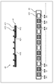
- FIG. 13 is a plan view showing a configuration example of the first display of the display device according to the first modification of the second embodiment.
- FIG. 14 is a diagram schematically showing the arrangement configuration of the first display and the second display in the first modification of the second embodiment.
- a 14-14 cross section of FIG. 13 that is, a cross section in the thickness direction (emission light direction) of the display device 40 is schematically shown.
- a configuration example 1 of the first display an example using a self-luminous display device is shown.
- the first display 41 (an example of the first display unit) is composed of a self-luminous display device such as an organic EL display, an inorganic EL display, an LED display, a plasma display, and a cathode ray tube.
- the first display 41 has an RGB light emitting element unit 412 in each pixel 411.
- the light emitting element unit 412 is connected to drive electrodes 413 and 414 provided in the vertical and horizontal two-dimensional pixel arrangement directions, and the light emitting element unit 412 of each pixel is driven to light up in response to a drive signal.
- a light-shielding portion 415 that blocks light is provided on the surface (lower surface of FIG. 14) of each pixel 411 on the second display 43 side.
- a circular or polygonal translucent portion 416 is provided for each predetermined unit of the plurality of pixels 411, and pinholes 421 by the translucent portions 416 are arranged and formed in two dimensions vertically and horizontally at predetermined intervals to form a pinhole array. (An example of an optical element array) is configured.
- a plurality of pixels 431 are arranged in two dimensions vertically and horizontally.
- RGB pixels are arranged in order, for example, pixels R1, G1, B1, ... Rn, Gn, Bn, ....
- a light field display is composed of a pinhole array formed by pinholes 421 formed on the first display 41 and a second display 43.
- the display of the image by the light field display is the same as that of the first embodiment.
- a microlens array may be provided as the optical element array. The configuration of the second modification in which the microlens array is provided between the first display and the second display is shown below.
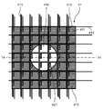
- FIG. 15 is a plan view showing a configuration example of the first display of the display device according to the second modification of the second embodiment.
- FIG. 16 is a diagram schematically showing the arrangement configuration of the first display and the second display in the second modification of the second embodiment.
- the first display 41a shown in FIG. 16 schematically shows a cross section of 16-16 of FIG. 15, that is, a cross section of the display device 40a in the thickness direction (emission light direction).
- the display device 40a of the modified example 2 shown in FIG. 15 has a light-shielding portion 415 and a pin arranged on the surface (lower surface of FIG. 14) of the first display 41 on the second display 43 side in the display device 40 of the modified example 1. This is a configuration in which the hall 421 is eliminated.
- the first display 41a (an example of the first display unit) is configured by using a member in which parts other than the light emitting element unit 412 and the drive electrodes 413 and 414 are completely transparent or translucent.
- the display device 40a has a structure in which a microlens array 423 in which a plurality of microlenses are arranged at a constant pitch (interval) is provided between the first display 41a and the second display 43.
- the light field display 15 is configured by the second display 43 and the microlens array 423.
- FIG. 17 is a diagram showing an example of texture display in the display device according to the first modification of the second embodiment.
- the emitted light 417 is emitted from each pixel 411. Further, in the plurality of pixels 431 of the second display 43, the emission direction of the light flux passing through the pinhole 421 differs depending on the position of the lit pixel, and the emitted light is emitted in a different direction according to the pixel position.
- pixel R1 is lit for red R
- pixels G2 and G3 are lit for green G
- pixel B4 is lit for blue B.
- hatched or white pixels represent lit pixels
- black pixels represent extinguished pixels (non-lit pixels).
- the emitted luminous flux 435R1 of the red pixel R1 passes through the pinhole 421 and is emitted obliquely upward to the right in FIG.
- the emitted luminous flux 435G2 of the green pixel G2 passes through the pinhole 421 and is emitted upward to the right in FIG.
- the emitted luminous flux 435G3 of the pixel G3 passes through the pinhole 421 and is emitted to the upward left in FIG. Will be done. Further, the emitted luminous flux 435B4 of the blue pixel B4 passes through the pinhole 421 and is emitted in the diagonally upward left direction in FIG.
- the display device 40 has been described above as an example, the same effect can be obtained for the display devices 30 and 40a.
- the size of one pixel of the second displays 33 and 43 is smaller than the distance between the plurality of pinholes 321 and 421.
- the size of one pixel of the first displays 31 and 41 is smaller than the distance between the plurality of pinholes 321 and 421 of the pinhole array. That is, the resolution of the first display is made higher than the resolution of the light field display by the second display.
- a high-resolution image can be displayed on the first display, and an image with a directional texture can be reproduced on the second display to supplement the resolution of the light field display, and the object to be displayed can be refined. It is possible to express with a realistic texture.
- the finer the pixel size of the first display the higher the resolution of the image quality.
- the finer the pixel size of the second display the greater the number of light rays that pass through the pinhole and emit light rays in different directions. Therefore, for example, if the distance from the pinhole is narrowed, the viewing area becomes larger. A wide (more obliquely visible) image is obtained.
- the pixels of the second display and the pinholes are at the same interval, if the size of the pixels is made finer, a finer texture change can be reproduced.
- the relationship between the size of one pixel of the second displays 33 and 43 in the display devices 30 and 40 and the spacing between the plurality of pinholes 321 and 421 has been described above, but the size of one pixel of the second display 43a in the display devices 40a has been described. The same applies to the relationship between the above and the arrangement pitch (interval) of the microlenses in the microlens array 423.
- the display surface of the first display, the second display, and the light field display by the pinhole array are arranged so as to overlap each other to form a display device.
- the orientation-independent non-directional display image displayed on the first display and the orientation-dependent display image displayed on the second display are superimposed and displayed by the light field display. It is possible to project a display image that expresses the texture. Therefore, in addition to the high-definition image on the display surface of the first display, an image having a different texture depending on the observation direction by the light field display can be recognizablely reproduced, and the observer can recognize a highly realistic target object having a fine texture. The image can be reproduced so that it can be visually recognized.
- FIG. 18 is a plan view showing a configuration example of the first display of the display device according to the third embodiment.
- FIG. 19 is a diagram schematically showing the arrangement configuration of the first display and the second display in the third embodiment.
- the first display 51 shown in FIG. 19 schematically shows a 19-1 cross section of FIG. 18, that is, a cross section of the display device 50 in the thickness direction (emission light direction).
- the third embodiment shows another specific example of the configuration of the display in the display device.
- a configuration example 2 of the first display an example using a reflective display device is shown.
- components different from those of the second embodiment will be mainly described, and duplicate description will be omitted.
- the first display 51 (an example of the first display unit) is composed of a reflective display device such as an electrophoretic electronic paper.
- a reflective display device such as a microcapsule system, a reflective liquid crystal system, an electrowetting system, or an electrochromic system may be used.
- a microcapsule type black-and-white display will be described for simplicity, but the same applies to a color display.
- the first display 51 has an image display unit 515 that displays white or black on each pixel 511.
- the image display unit 515 is connected to drive electrodes 513 and 514 of transparent electrodes provided in the vertical and horizontal two-dimensional pixel arrangement directions, and the image display unit 515 of each pixel is driven according to the drive signal to drive the white display unit 515w.
- a black display unit 515b is formed.
- a circular or polygonal translucent portion 516 is provided for each predetermined unit of the plurality of pixels 511, and pinholes 521 by the translucent portions 516 are arranged and formed in two dimensions vertically and horizontally at predetermined intervals to form a pinhole array. (An example of an optical element array) is configured.
- a plurality of pixels 531 are arranged in two dimensions vertically and horizontally.
- RGB pixels are arranged in order, for example, pixels R1, G1, B1, ... Rn, Gn, Bn, ....
- a light field display is composed of a pinhole array formed by pinholes 521 formed on the first display 51 and a second display 53.
- the arrangement configuration of the pinhole array and the pixel 531 of the second display 53 is the same as that of the first embodiment and the second embodiment.
- FIG. 20 is a diagram showing an example of texture display in the display device of the third embodiment.
- a plurality of pixels 511 of the first display 51 are driven to form a white display unit 515w or a black display unit 515b.
- the external light 301 is reflected by the outer surface of the first display 51, and the scattered light 517 of the external light by the electronic paper is emitted to the outside at the white display unit 515w.
- External light is absorbed by the black display unit 515b.
- a black-and-white image produced by electronic paper is displayed and visually recognized by the observer.
- the emission direction of the light flux passing through the pinhole 521 differs depending on the position of the lit pixel, and the emitted light is emitted in a different direction according to the pixel position.
- pixel R1 is lit for red R
- pixels G2 and G3 are lit for green G
- pixel B4 is lit for blue B.
- hatched or white pixels represent lit pixels
- black pixels represent extinguished pixels (non-lit pixels).
- the emitted luminous flux 535R1 of the red pixel R1 passes through the pinhole 521 and is emitted obliquely upward to the right in FIG.
- the emitted luminous flux 535G2 of the green pixel G2 passes through the pinhole 521 and is emitted upward to the right in FIG.
- the emitted luminous flux 535G3 of the pixel G3 passes through the pinhole 521 and is emitted to the upward left in FIG. Will be done. Further, the luminous flux 535B4 of the blue pixel B4 passes through the pinhole 521 and is emitted in the diagonally upward left direction in FIG.
- the display surface of the first display and the light field display by the second display and the pinhole array are arranged so as to form a display device.
- the non-directional display image displayed on the electronic paper of the first display and the directional display image displayed on the second display depending on the orientation are superimposed, and the texture of the light field display is obtained. It is possible to project a display image that expresses. Therefore, it is possible for the observer to visually reproduce an image of a highly realistic target object in which a texture is added to a high-definition display image of electronic paper.
- the present embodiment it is possible to reproduce the image of the target object by adding different brilliance, reflected light, shadow, color, and stereoscopic effect depending on the viewing direction of the observer.
- the display devices of the first to third embodiments include a first display unit such as a decorative layer or a display having a non-directional display surface that is invariant regardless of the viewing direction of the observer, and a first display device.
- a second display unit which is arranged on the side opposite to the outer surface of the display unit and displays an image having different directions depending on the viewing direction of the observer, is provided.
- the second display unit has a display in which a plurality of pixels are arranged two-dimensionally.
- the display device is arranged between the outer surface of the first display unit and the second display unit in parallel with the light emitting surface of the display, and optical elements such as a plurality of pinholes correspond to pixels of a predetermined unit. It includes an array of arranged optical elements.
- a light field display is composed of these displays and an array of optical elements. Further, the display device includes a drive unit that drives the display to light a predetermined pixel. As a result, the image provided on the display surface of the first display unit and the image obtained by the light field display can be combined so that the observer can recognize and reproduce an image having an appropriate texture.
- the first display unit is composed of a decorative layer whose outer surface is decorated as a non-directional display surface.
- the texture has directionality by the second display unit. The image can be reproduced and the observer can recognize the appropriate texture.
- the optical element array is composed of a pinhole array in which a plurality of pinholes are arranged two-dimensionally at predetermined intervals, and the pinholes penetrate the outer surface of the first display unit. Is formed.
- the direction of the light rays emitted through the pinhole array can be controlled according to the pixel positions lit by the display of the second display unit, and the light rays emitted in a predetermined direction can be reproduced. For example, it is possible to emit light rays in different directions according to colors such as RGB, and reproduce images of different colors depending on the viewing direction of the observer.
- the first display unit includes a first display for displaying a non-directional display image
- the second display unit is a predetermined of a plurality of pixels. It has a second display for lighting the pixels at the pixel positions of the above
- the drive unit has a first display drive circuit for driving the first display and a second display drive circuit for driving the second display.
- the first display is formed with light-transmitting portions that transmit light to the outer surface at predetermined intervals
- the optical element array is a plurality of optical element arrays formed by the light-transmitting portions of the first display.
- the pinholes are composed of a two-dimensionally arranged pinhole array.
- the first display is composed of a self-luminous display device or a reflective display device. As a result, a high-definition display image with high visibility can be displayed on the first display.
- the size of one pixel of the display of the second display unit is smaller than the distance between a plurality of pinholes in the pinhole array.
- the size of one pixel of the first display is smaller than the distance between a plurality of pinholes in the pinhole array
- the size of one pixel of the second display is a pin. It is smaller than the spacing between multiple pinholes in the hole array.
- the display of the second display unit lights a pixel at a predetermined pixel position among the plurality of pixels and controls the direction of the light beam emitted through the optical element array. , Reproduces a display image in which at least one of the wavelength and brightness of light differs depending on the viewing direction of the observer. As a result, it is possible to reproduce an image having different colors and brightness depending on the viewing direction of the observer, to form an image having a texture close to that of a real object imitating an object object, and to make the observer visually recognize the image.
- the display of the second display unit is a display image visually recognized in the position of the outer surface of the first display unit or in the space on the observer side from the outer surface from the viewpoint of the observer. To reproduce. As a result, it is possible to display an image having a texture such as gloss on the outer surface of the first display unit, or to reproduce an image having unevenness so as to protrude forward from the first display unit. It is possible to realize an image in which the observer can recognize an appropriate texture.
- the display of the second display unit reproduces a stereoscopic image as a display image.
- the observer can visually recognize a stereoscopic image with a high sense of presence, and the expressive power of the display image by the display device can be improved.
- the present disclosure is useful as a display device or the like capable of recognizablely reproducing an image having an appropriate texture by an observer by combining an image provided on a display surface and an image by a light field display.
- Display device 11 Decorative layer 12 Pinhole film 13 Display 15, 35 Light field display 31, 41, 41a, 51 First display 33, 43, 53 Second display 60
- Display drive circuit 61 1st display drive circuit 63 2nd display drive circuit 90
- Control device 91 Light source direction calculation circuit 92
- Display object data storage unit 93
- Ray tracing calculation circuit 95
- Non-directional image drawing calculation circuit 96
- Directional image drawing calculation Circuit 105, 105a, 105b, 105c Viewpoint 121, 321, 421, 521 Pinhole 122,322 Pinhole Array 131,411,431,511,531 Pixels 210
- Light source direction / light source wavelength characteristic identification device 301 External light 412 415 Light-shielding part 416, 516 Translucent part 423
- Micro lens array 515 Image display part 515b Black display part 515w White display part
Landscapes
- Physics & Mathematics (AREA)
- Engineering & Computer Science (AREA)
- Multimedia (AREA)
- Signal Processing (AREA)
- General Physics & Mathematics (AREA)
- Optics & Photonics (AREA)
- Devices For Indicating Variable Information By Combining Individual Elements (AREA)
- Testing, Inspecting, Measuring Of Stereoscopic Televisions And Televisions (AREA)
- Controls And Circuits For Display Device (AREA)
Priority Applications (5)
| Application Number | Priority Date | Filing Date | Title |
|---|---|---|---|
| US17/632,100 US20220279157A1 (en) | 2019-08-02 | 2020-06-05 | Display device |
| CN202080053095.7A CN114144719A (zh) | 2019-08-02 | 2020-06-05 | 显示装置 |
| JP2021537602A JP7316594B2 (ja) | 2019-08-02 | 2020-06-05 | 表示装置 |
| EP20850670.9A EP4009096A4 (en) | 2019-08-02 | 2020-06-05 | INDICATOR |
| JP2023110906A JP7542228B2 (ja) | 2019-08-02 | 2023-07-05 | 表示装置 |
Applications Claiming Priority (2)
| Application Number | Priority Date | Filing Date | Title |
|---|---|---|---|
| JP2019143220 | 2019-08-02 | ||
| JP2019-143220 | 2019-08-02 |
Publications (1)
| Publication Number | Publication Date |
|---|---|
| WO2021024600A1 true WO2021024600A1 (ja) | 2021-02-11 |
Family
ID=74502587
Family Applications (1)
| Application Number | Title | Priority Date | Filing Date |
|---|---|---|---|
| PCT/JP2020/022224 Ceased WO2021024600A1 (ja) | 2019-08-02 | 2020-06-05 | 表示装置 |
Country Status (5)
| Country | Link |
|---|---|
| US (1) | US20220279157A1 (enExample) |
| EP (1) | EP4009096A4 (enExample) |
| JP (2) | JP7316594B2 (enExample) |
| CN (1) | CN114144719A (enExample) |
| WO (1) | WO2021024600A1 (enExample) |
Cited By (2)
| Publication number | Priority date | Publication date | Assignee | Title |
|---|---|---|---|---|
| JP2023009467A (ja) * | 2021-07-07 | 2023-01-20 | 凸版印刷株式会社 | 画像表示装置およびヘッドマウントディスプレイ |
| JPWO2023223623A1 (enExample) * | 2022-05-17 | 2023-11-23 |
Families Citing this family (1)
| Publication number | Priority date | Publication date | Assignee | Title |
|---|---|---|---|---|
| EP4336483A1 (en) * | 2022-09-06 | 2024-03-13 | Continental Automotive Technologies GmbH | Display device, method, computer program code, and apparatus for providing a correction map for a display device, method and computer program code for operating a display device |
Citations (5)
| Publication number | Priority date | Publication date | Assignee | Title |
|---|---|---|---|---|
| JP2001235708A (ja) * | 2000-02-22 | 2001-08-31 | Japan Science & Technology Corp | 背景付き立体像再生装置 |
| JP3124951U (ja) | 2000-12-26 | 2006-09-07 | 永恩 林 | 多機能付き輝度差装飾スクリーン |
| JP2008009046A (ja) * | 2006-06-28 | 2008-01-17 | Osaka Univ | 三次元画像再生装置 |
| KR20090041303A (ko) * | 2007-10-23 | 2009-04-28 | 재단법인서울대학교산학협력재단 | 동적 핀홀 어레이를 이용한 입체 영상 시스템 및 그 영상표시 방법 |
| JP2010072632A (ja) * | 2008-09-19 | 2010-04-02 | Samsung Electronics Co Ltd | 2次元と3次元兼用映像表示装置および方法 |
Family Cites Families (11)
| Publication number | Priority date | Publication date | Assignee | Title |
|---|---|---|---|---|
| JP2004241962A (ja) * | 2003-02-05 | 2004-08-26 | Pioneer Electronic Corp | 表示装置及び方法 |
| KR20080105026A (ko) * | 2006-02-10 | 2008-12-03 | 미라이얼 가부시키가이샤 | 광학 시트, 화상표시장치 및 화상투사장치용 스크린 |
| JP5248062B2 (ja) * | 2007-08-24 | 2013-07-31 | 株式会社東芝 | 指向性バックライト、表示装置及び立体画像表示装置 |
| TW201334510A (zh) * | 2012-02-07 | 2013-08-16 | Wintek Corp | 裸眼與眼鏡可切換式立體顯示裝置 |
| CN102608768B (zh) * | 2012-03-31 | 2015-10-14 | 福州大学 | 基于led的双面光栅立体显示装置及其制作方法 |
| TW201500805A (zh) * | 2013-06-25 | 2015-01-01 | Wintek Corp | 液晶透鏡、立體顯示裝置與其顯示方法 |
| CN106405849B (zh) * | 2015-07-30 | 2019-05-28 | 华为技术有限公司 | 立体成像装置和用户终端 |
| JP6588840B2 (ja) * | 2016-02-04 | 2019-10-09 | 株式会社ジャパンディスプレイ | 表示装置 |
| EP3642692B1 (en) * | 2017-06-30 | 2021-10-13 | Huawei Technologies Co., Ltd. | System and method for interacting with a user via a mirror |
| CN111752339B (zh) * | 2019-03-28 | 2023-02-28 | 北京小米移动软件有限公司 | 一种终端 |
| KR102669182B1 (ko) * | 2020-01-30 | 2024-05-28 | 삼성디스플레이 주식회사 | 광 투과 영역을 포함하는 표시 장치, 및 전자 기기 |
-
2020
- 2020-06-05 US US17/632,100 patent/US20220279157A1/en not_active Abandoned
- 2020-06-05 JP JP2021537602A patent/JP7316594B2/ja active Active
- 2020-06-05 WO PCT/JP2020/022224 patent/WO2021024600A1/ja not_active Ceased
- 2020-06-05 CN CN202080053095.7A patent/CN114144719A/zh active Pending
- 2020-06-05 EP EP20850670.9A patent/EP4009096A4/en not_active Withdrawn
-
2023
- 2023-07-05 JP JP2023110906A patent/JP7542228B2/ja active Active
Patent Citations (5)
| Publication number | Priority date | Publication date | Assignee | Title |
|---|---|---|---|---|
| JP2001235708A (ja) * | 2000-02-22 | 2001-08-31 | Japan Science & Technology Corp | 背景付き立体像再生装置 |
| JP3124951U (ja) | 2000-12-26 | 2006-09-07 | 永恩 林 | 多機能付き輝度差装飾スクリーン |
| JP2008009046A (ja) * | 2006-06-28 | 2008-01-17 | Osaka Univ | 三次元画像再生装置 |
| KR20090041303A (ko) * | 2007-10-23 | 2009-04-28 | 재단법인서울대학교산학협력재단 | 동적 핀홀 어레이를 이용한 입체 영상 시스템 및 그 영상표시 방법 |
| JP2010072632A (ja) * | 2008-09-19 | 2010-04-02 | Samsung Electronics Co Ltd | 2次元と3次元兼用映像表示装置および方法 |
Cited By (3)
| Publication number | Priority date | Publication date | Assignee | Title |
|---|---|---|---|---|
| JP2023009467A (ja) * | 2021-07-07 | 2023-01-20 | 凸版印刷株式会社 | 画像表示装置およびヘッドマウントディスプレイ |
| JP7742072B2 (ja) | 2021-07-07 | 2025-09-19 | Toppanホールディングス株式会社 | 画像表示装置およびヘッドマウントディスプレイ |
| JPWO2023223623A1 (enExample) * | 2022-05-17 | 2023-11-23 |
Also Published As
| Publication number | Publication date |
|---|---|
| JP2023145466A (ja) | 2023-10-11 |
| JP7316594B2 (ja) | 2023-07-28 |
| JPWO2021024600A1 (enExample) | 2021-02-11 |
| US20220279157A1 (en) | 2022-09-01 |
| EP4009096A1 (en) | 2022-06-08 |
| EP4009096A4 (en) | 2022-09-14 |
| CN114144719A (zh) | 2022-03-04 |
| JP7542228B2 (ja) | 2024-08-30 |
Similar Documents
| Publication | Publication Date | Title |
|---|---|---|
| JP7542228B2 (ja) | 表示装置 | |
| JP5651840B2 (ja) | 図柄表示装置 | |
| US20060265919A1 (en) | Transparent light-conducting module | |
| US20160240118A1 (en) | 3-d display using led pixel layers | |
| US10535291B2 (en) | Display device and control method thereof, and display system | |
| WO2016104340A1 (ja) | 表示装置及びその駆動方法 | |
| JP4676424B2 (ja) | ディミング装置 | |
| JPWO2021024600A5 (enExample) | ||
| JP2005501275A (ja) | 視覚表示装置及び視覚表示パネルを動作する方法 | |
| JP7676057B2 (ja) | 表示装置 | |
| TWI680447B (zh) | 顯示裝置及其驅動方法 | |
| KR20180009307A (ko) | 투명 전광판 장치 | |
| JP6618641B2 (ja) | 質感表示装置、質感表示方法、及び質感表示プログラム | |
| JP2009265309A (ja) | 三次元画像表示装置 | |
| TWI874058B (zh) | 多層顯示模組 | |
| JP7644905B1 (ja) | 加飾シート及び表示システム | |
| US9762892B2 (en) | Auto-multiscopic 3D display and camera system | |
| TWI723530B (zh) | 顯示裝置及其驅動方法 | |
| CN120164388A (zh) | 显示面板及显示装置 | |
| TW202422514A (zh) | 具有高對比度的廣告裝置 | |
| KR20250027349A (ko) | 표시장치 | |
| JP2006267390A (ja) | 表示装置並びに発光素子の製造方法 | |
| JP2008116878A (ja) | 画像表示装置 | |
| JP2022022466A (ja) | 錯視模様シート、錯視模様シートの製造方法及び3次元映像表示装置 | |
| RU158993U1 (ru) | Рекламная панель с комбинированной подсветкой |
Legal Events
| Date | Code | Title | Description |
|---|---|---|---|
| 121 | Ep: the epo has been informed by wipo that ep was designated in this application |
Ref document number: 20850670 Country of ref document: EP Kind code of ref document: A1 |
|
| ENP | Entry into the national phase |
Ref document number: 2021537602 Country of ref document: JP Kind code of ref document: A |
|
| NENP | Non-entry into the national phase |
Ref country code: DE |
|
| ENP | Entry into the national phase |
Ref document number: 2020850670 Country of ref document: EP Effective date: 20220302 |