WO2021024508A1 - 発光装置、光学装置及び情報処理装置 - Google Patents
発光装置、光学装置及び情報処理装置 Download PDFInfo
- Publication number
- WO2021024508A1 WO2021024508A1 PCT/JP2019/048789 JP2019048789W WO2021024508A1 WO 2021024508 A1 WO2021024508 A1 WO 2021024508A1 JP 2019048789 W JP2019048789 W JP 2019048789W WO 2021024508 A1 WO2021024508 A1 WO 2021024508A1
- Authority
- WO
- WIPO (PCT)
- Prior art keywords
- light
- light emitting
- light source
- emitting device
- vcsel
- Prior art date
- Legal status (The legal status is an assumption and is not a legal conclusion. Google has not performed a legal analysis and makes no representation as to the accuracy of the status listed.)
- Ceased
Links
Images






Classifications
-
- G—PHYSICS
- G06—COMPUTING OR CALCULATING; COUNTING
- G06V—IMAGE OR VIDEO RECOGNITION OR UNDERSTANDING
- G06V40/00—Recognition of biometric, human-related or animal-related patterns in image or video data
- G06V40/10—Human or animal bodies, e.g. vehicle occupants or pedestrians; Body parts, e.g. hands
- G06V40/16—Human faces, e.g. facial parts, sketches or expressions
- G06V40/161—Detection; Localisation; Normalisation
- G06V40/166—Detection; Localisation; Normalisation using acquisition arrangements
-
- G—PHYSICS
- G01—MEASURING; TESTING
- G01S—RADIO DIRECTION-FINDING; RADIO NAVIGATION; DETERMINING DISTANCE OR VELOCITY BY USE OF RADIO WAVES; LOCATING OR PRESENCE-DETECTING BY USE OF THE REFLECTION OR RERADIATION OF RADIO WAVES; ANALOGOUS ARRANGEMENTS USING OTHER WAVES
- G01S17/00—Systems using the reflection or reradiation of electromagnetic waves other than radio waves, e.g. lidar systems
- G01S17/88—Lidar systems specially adapted for specific applications
- G01S17/89—Lidar systems specially adapted for specific applications for mapping or imaging
-
- G—PHYSICS
- G01—MEASURING; TESTING
- G01S—RADIO DIRECTION-FINDING; RADIO NAVIGATION; DETERMINING DISTANCE OR VELOCITY BY USE OF RADIO WAVES; LOCATING OR PRESENCE-DETECTING BY USE OF THE REFLECTION OR RERADIATION OF RADIO WAVES; ANALOGOUS ARRANGEMENTS USING OTHER WAVES
- G01S7/00—Details of systems according to groups G01S13/00, G01S15/00, G01S17/00
- G01S7/48—Details of systems according to groups G01S13/00, G01S15/00, G01S17/00 of systems according to group G01S17/00
- G01S7/481—Constructional features, e.g. arrangements of optical elements
-
- G—PHYSICS
- G02—OPTICS
- G02B—OPTICAL ELEMENTS, SYSTEMS OR APPARATUS
- G02B5/00—Optical elements other than lenses
- G02B5/02—Diffusing elements; Afocal elements
-
- G—PHYSICS
- G03—PHOTOGRAPHY; CINEMATOGRAPHY; ANALOGOUS TECHNIQUES USING WAVES OTHER THAN OPTICAL WAVES; ELECTROGRAPHY; HOLOGRAPHY
- G03B—APPARATUS OR ARRANGEMENTS FOR TAKING PHOTOGRAPHS OR FOR PROJECTING OR VIEWING THEM; APPARATUS OR ARRANGEMENTS EMPLOYING ANALOGOUS TECHNIQUES USING WAVES OTHER THAN OPTICAL WAVES; ACCESSORIES THEREFOR
- G03B15/00—Special procedures for taking photographs; Apparatus therefor
- G03B15/02—Illuminating scene
-
- G—PHYSICS
- G03—PHOTOGRAPHY; CINEMATOGRAPHY; ANALOGOUS TECHNIQUES USING WAVES OTHER THAN OPTICAL WAVES; ELECTROGRAPHY; HOLOGRAPHY
- G03B—APPARATUS OR ARRANGEMENTS FOR TAKING PHOTOGRAPHS OR FOR PROJECTING OR VIEWING THEM; APPARATUS OR ARRANGEMENTS EMPLOYING ANALOGOUS TECHNIQUES USING WAVES OTHER THAN OPTICAL WAVES; ACCESSORIES THEREFOR
- G03B15/00—Special procedures for taking photographs; Apparatus therefor
- G03B15/02—Illuminating scene
- G03B15/03—Combinations of cameras with lighting apparatus; Flash units
-
- G—PHYSICS
- G03—PHOTOGRAPHY; CINEMATOGRAPHY; ANALOGOUS TECHNIQUES USING WAVES OTHER THAN OPTICAL WAVES; ELECTROGRAPHY; HOLOGRAPHY
- G03B—APPARATUS OR ARRANGEMENTS FOR TAKING PHOTOGRAPHS OR FOR PROJECTING OR VIEWING THEM; APPARATUS OR ARRANGEMENTS EMPLOYING ANALOGOUS TECHNIQUES USING WAVES OTHER THAN OPTICAL WAVES; ACCESSORIES THEREFOR
- G03B15/00—Special procedures for taking photographs; Apparatus therefor
- G03B15/02—Illuminating scene
- G03B15/03—Combinations of cameras with lighting apparatus; Flash units
- G03B15/05—Combinations of cameras with electronic flash apparatus; Electronic flash units
-
- G—PHYSICS
- G03—PHOTOGRAPHY; CINEMATOGRAPHY; ANALOGOUS TECHNIQUES USING WAVES OTHER THAN OPTICAL WAVES; ELECTROGRAPHY; HOLOGRAPHY
- G03B—APPARATUS OR ARRANGEMENTS FOR TAKING PHOTOGRAPHS OR FOR PROJECTING OR VIEWING THEM; APPARATUS OR ARRANGEMENTS EMPLOYING ANALOGOUS TECHNIQUES USING WAVES OTHER THAN OPTICAL WAVES; ACCESSORIES THEREFOR
- G03B35/00—Stereoscopic photography
-
- G—PHYSICS
- G06—COMPUTING OR CALCULATING; COUNTING
- G06V—IMAGE OR VIDEO RECOGNITION OR UNDERSTANDING
- G06V10/00—Arrangements for image or video recognition or understanding
- G06V10/10—Image acquisition
- G06V10/12—Details of acquisition arrangements; Constructional details thereof
- G06V10/14—Optical characteristics of the device performing the acquisition or on the illumination arrangements
- G06V10/141—Control of illumination
-
- G—PHYSICS
- G06—COMPUTING OR CALCULATING; COUNTING
- G06V—IMAGE OR VIDEO RECOGNITION OR UNDERSTANDING
- G06V10/00—Arrangements for image or video recognition or understanding
- G06V10/10—Image acquisition
- G06V10/12—Details of acquisition arrangements; Constructional details thereof
- G06V10/14—Optical characteristics of the device performing the acquisition or on the illumination arrangements
- G06V10/147—Details of sensors, e.g. sensor lenses
-
- G—PHYSICS
- G06—COMPUTING OR CALCULATING; COUNTING
- G06V—IMAGE OR VIDEO RECOGNITION OR UNDERSTANDING
- G06V10/00—Arrangements for image or video recognition or understanding
- G06V10/40—Extraction of image or video features
- G06V10/42—Global feature extraction by analysis of the whole pattern, e.g. using frequency domain transformations or autocorrelation
- G06V10/422—Global feature extraction by analysis of the whole pattern, e.g. using frequency domain transformations or autocorrelation for representing the structure of the pattern or shape of an object therefor
-
- G—PHYSICS
- G06—COMPUTING OR CALCULATING; COUNTING
- G06V—IMAGE OR VIDEO RECOGNITION OR UNDERSTANDING
- G06V10/00—Arrangements for image or video recognition or understanding
- G06V10/70—Arrangements for image or video recognition or understanding using pattern recognition or machine learning
- G06V10/74—Image or video pattern matching; Proximity measures in feature spaces
-
- H—ELECTRICITY
- H01—ELECTRIC ELEMENTS
- H01S—DEVICES USING THE PROCESS OF LIGHT AMPLIFICATION BY STIMULATED EMISSION OF RADIATION [LASER] TO AMPLIFY OR GENERATE LIGHT; DEVICES USING STIMULATED EMISSION OF ELECTROMAGNETIC RADIATION IN WAVE RANGES OTHER THAN OPTICAL
- H01S5/00—Semiconductor lasers
- H01S5/10—Construction or shape of the optical resonator, e.g. extended or external cavity, coupled cavities, bent-guide, varying width, thickness or composition of the active region
- H01S5/18—Surface-emitting [SE] lasers, e.g. having both horizontal and vertical cavities
- H01S5/183—Surface-emitting [SE] lasers, e.g. having both horizontal and vertical cavities having only vertical cavities, e.g. vertical cavity surface-emitting lasers [VCSEL]
-
- H—ELECTRICITY
- H01—ELECTRIC ELEMENTS
- H01S—DEVICES USING THE PROCESS OF LIGHT AMPLIFICATION BY STIMULATED EMISSION OF RADIATION [LASER] TO AMPLIFY OR GENERATE LIGHT; DEVICES USING STIMULATED EMISSION OF ELECTROMAGNETIC RADIATION IN WAVE RANGES OTHER THAN OPTICAL
- H01S5/00—Semiconductor lasers
- H01S5/40—Arrangement of two or more semiconductor lasers, not provided for in groups H01S5/02 - H01S5/30
- H01S5/42—Arrays of surface emitting lasers
-
- H—ELECTRICITY
- H04—ELECTRIC COMMUNICATION TECHNIQUE
- H04N—PICTORIAL COMMUNICATION, e.g. TELEVISION
- H04N13/00—Stereoscopic video systems; Multi-view video systems; Details thereof
- H04N13/30—Image reproducers
- H04N13/302—Image reproducers for viewing without the aid of special glasses, i.e. using autostereoscopic displays
- H04N13/307—Image reproducers for viewing without the aid of special glasses, i.e. using autostereoscopic displays using fly-eye lenses, e.g. arrangements of circular lenses
-
- G—PHYSICS
- G06—COMPUTING OR CALCULATING; COUNTING
- G06V—IMAGE OR VIDEO RECOGNITION OR UNDERSTANDING
- G06V2201/00—Indexing scheme relating to image or video recognition or understanding
- G06V2201/12—Acquisition of 3D measurements of objects
Definitions
- the present invention relates to a light emitting device, an optical device, and an information processing device.
- Patent Document 1 has a light source, a plurality of lenses arranged adjacent to each other on a predetermined plane, a diffuser plate for diffusing the light emitted by the light source, and light diffused by the diffuser plate as a subject.
- An imaging device including an imaging element that receives the reflected reflected light and a plurality of lenses arranged so that the period of interference fringes in the diffused light is three pixels or less is described.
- the light emitted from the light source is diffused and irradiated in a predetermined range with a predetermined light intensity distribution. Is required to do. At this time, the light reaches outside the predetermined range while gradually attenuating the intensity, but the light reaching outside the predetermined range is wasted.
- An object of the present invention is to provide a light emitting device or the like that suppresses the amount of light that reaches outside a predetermined range as compared with the case where the spreading angle of the light emitted by the light emitting element of the light source is not narrowed.
- the light emitting device is provided in a light source in which a plurality of light emitting elements are arranged and a light emitting path of the light source, and emits light by narrowing the spread angle of the emitted light from each light emitting element in the light source. It is characterized by including a first optical member and a second optical member provided on the light emitting side of the first optical member and diffusing and irradiating light incident from the first optical member side. And.
- the light emitting device is the light emitting device according to the first aspect, wherein the first optical member is an optical component that narrows the spreading angle of light by refraction.
- the light emitting device is the light emitting device according to the second aspect, wherein the first optical member is provided on a light emitting element of the light source.
- the light emitting device according to the fourth aspect of the present invention is the light emitting device according to the third aspect, wherein the first optical member is a microlens provided for each light emitting element of the light source.
- the light emitting device according to the fifth aspect of the present invention is characterized in that, in the light emitting device according to the first aspect, the first optical member emits light incident from each light emitting element of the light source as parallel light. To do.
- the light emitting device is the light emitting device according to the first aspect, wherein the light emitting element is a vertical resonance type surface emitting laser element.
- the light emitting device according to the seventh aspect of the present invention is the light emitting device according to the sixth aspect, wherein the vertical resonance type surface emitting laser element has a long resonator structure.
- the light emitting device according to the eighth aspect of the present invention is the light emitting device according to any one of the first to seventh aspects, wherein the plurality of the light emitting elements are connected in parallel to each other by an electrode pattern, and the electrode pattern is The region excluding the output port of each light emitting element is covered with a continuous pattern.
- the light emitting device is the light emitting device according to any one of the first to eighth aspects, wherein the second optical member changes the directivity of the light emitted from the first optical member. It is characterized in that it is irradiated with light.
- the light emitting device according to the tenth aspect of the present invention is the light emitting device according to the ninth aspect, and the invention according to claim 10 is a plate-shaped member in the second optical member, and at least one of them. It is characterized in that the surface is provided with a structure that changes the directivity of light.
- the light emitting device is the light emitting device according to any one of the first to ninth aspects, wherein the second optical member is a plate-shaped member, and a plurality of recesses are formed on at least one surface. And it is characterized in that a convex portion is provided.
- the light emitting device according to the twelfth aspect of the present invention is the light emitting device according to any one of the first to eleventh aspects, wherein the second optical member irradiates light used for measuring a three-dimensional shape by a time-of-flight method. It is characterized by doing.
- the light source, the first optical member, and the second optical member are used as a portable information processing terminal. It is mounted and the light source is driven by the battery of the portable information processing terminal.
- the light source device according to the fourteenth aspect of the present invention includes a light emitting device according to any one of the first to thirteenth aspects and a light receiving unit that receives reflected light emitted from the light source included in the light emitting device and reflected by the measurement target.
- the light receiving unit is characterized in that it outputs a signal corresponding to the time from when light is emitted from the light source to when the light is received by the light receiving unit.
- the information processing device is the reflected light emitted from the optical device according to the fourteenth aspect and the light source included in the optical device and reflected by the measurement target, and received by the light receiving unit included in the optical device. Based on this, it is characterized by including a shape specifying portion that specifies the three-dimensional shape of the measurement target.
- the information processing device according to the 16th aspect of the present invention further includes an authentication processing unit that performs an authentication process regarding the use of the own device based on the specific result in the shape specifying unit in the information processing device according to the 15th aspect. It is characterized by.
- the amount of light emitted outside the predetermined range is suppressed as compared with the case where the spreading angle of the light emitted by the light emitting element of the light source is not narrowed.
- the spread angle can be easily controlled as compared with the case where the first optical member is not an optical component that narrows the spread angle of light by refraction.
- the light emitting device can be downsized as compared with the case where the first optical member is not provided on the light emitting element of the light source.
- the amount of light emitted outside the predetermined range is larger than that in the case where the first optical member does not emit the light incident from each light emitting element of the light source as parallel light. It is suppressed.
- it is easier to form a surface emitting light source than in the case where the light emitting element is not a vertical resonance type surface emitting laser element.
- the spreading angle of the emitted light can be narrower than that in the case where the vertical resonance type surface emitting laser element does not have a long resonator structure.
- the voltage drop when the drive current flows is suppressed as compared with the case where the wiring is provided for each light emitting element.
- the light incident from the first optical member side is diffused as compared with the case where the second optical member does not change the directivity of the light emitted from the first optical member. Can be irradiated.
- the tenth aspect of the present invention as compared with the case where the structure for changing the directivity of light is not provided on at least one surface of the second optical member which is a plate-shaped member, from the first optical member side. The incident light can be diffused and irradiated.
- the second optical member provided with a plurality of concave portions and convex portions on at least one surface of the plate-shaped member can be easily manufactured, the light emitting element can be manufactured at low cost. Can be done. According to the twelfth aspect of the present invention, it is possible to increase the utilization efficiency of light used for measuring a three-dimensional shape by a time-of-flight method. According to the thirteenth aspect of the present invention, since the light utilization efficiency can be increased, the battery consumption can be suppressed and the driving time of the portable information processing terminal can be lengthened.
- an optical device capable of measuring the time from when light is emitted by a light emitting device to when it is received by a light receiving unit.
- an information processing device capable of measuring a three-dimensional shape is provided.
- an information processing apparatus equipped with an authentication process based on a three-dimensional shape is provided.
- FIG. 1 It is a figure which shows an example of the information processing apparatus to which 1st Embodiment is applied. It is a figure explaining the measurement of a three-dimensional shape by an information processing apparatus. It is a figure explaining the irradiation surface.
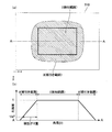
- (A) is a diagram showing an example of an irradiation pattern on an irradiation surface, and (b) is a light intensity distribution on the AA line of (a).
- (A) is a plan view
- (b) is a cross-sectional view taken along the line VB-VB of (a).
- the information processing device is its own device only when it identifies whether or not the user who has accessed the information processing device is permitted to access it and is authenticated as a user who is permitted to access the information processing device. In many cases, the use of information processing equipment is permitted. So far, a method of authenticating a user by a password, a fingerprint, an iris, or the like has been used. Recently, there is a demand for an authentication method with even higher security. As this method, authentication is performed using a three-dimensional image of the user's face.
- the information processing device will be described as an example of a portable information processing terminal, and will be described as authenticating a user by recognizing a face captured as a three-dimensional image.
- the information processing device can be applied to an information processing device such as a personal computer (PC) other than a portable information processing terminal.
- PC personal computer
- the configuration, function, method, etc. described in the present embodiment can be applied to the acquisition of a three-dimensional image of an object in addition to the recognition based on the shape of the face. That is, it may be applied to acquire a three-dimensional image by measuring the three-dimensional shape of the measurement target with an object other than the face as the measurement target.
- the distance to the measurement target (hereinafter referred to as the measurement distance) does not matter.
- a face or an object other than the face for which a three-dimensional image is to be acquired may be referred to as an irradiated object or an object to be measured.
- FIG. 1 is a diagram showing an example of an information processing apparatus 1 to which the first embodiment is applied.
- the information processing device 1 is, for example, a portable information processing terminal.
- the information processing device 1 includes a user interface unit (hereinafter, referred to as a UI unit) 2 and an optical device 3 for acquiring a three-dimensional image.
- the UI unit 2 is configured by integrating, for example, a display device that displays information to the user and an input device that inputs instructions for information processing by the user's operation.
- the display device is, for example, a liquid crystal display or an organic EL display
- the input device is, for example, a touch panel.
- the optical device 3 includes a light emitting device 4 and a three-dimensional sensor (hereinafter referred to as a 3D sensor) 6.
- the light emitting device 4 emits light toward a measurement target for measuring a three-dimensional shape for acquiring a three-dimensional image, a face in the example described here.
- the 3D sensor 6 acquires the light emitted by the light emitting device 4 and reflected by the face and returned.
- the optical device 3 acquires a three-dimensional image of a face based on a so-called time of flight (TOF) method based on the flight time of light.
- TOF time of flight
- the information processing device 1 is configured as a computer including a CPU, ROM, RAM, and the like.
- the ROM includes a non-volatile, rewritable memory, such as a flash memory.
- the programs and constants stored in the ROM are expanded in the RAM.
- the CPU executes the program expanded in the RAM, the information processing device 1 operates and various types of information processing are executed.
- FIG. 2 is a diagram illustrating measurement of a three-dimensional shape by the information processing device 1.
- the measurement target here is the face 300.
- the right direction of the paper surface is the x direction
- the upward direction is the z direction
- the back surface direction of the paper surface is the y direction.
- FIG. 2 is a view of the head (face) viewed from above.
- the optical device 3 of the information processing device 1 light is emitted from the light emitting device 4 toward the face 300. Then, the light reflected by the face 300 by the 3D sensor 6 is received. That is, the optical device 3 is configured such that light is emitted from the light emitting device 4 toward the measurement target and the reflected light from the measurement target is received by the 3D sensor 6. At this time, the light emitting device 4 irradiates light toward the irradiation surface 310, which is a virtual surface provided facing the light emitting device 4.
- the light emitting device 4 and the irradiation surface 310 face each other, and the light emitting device 4 is located on the perpendicular line 321 standing on the irradiation surface 310.
- the perpendicular line 321 stands at the center of the detection range I described later.
- the AA line is a line that passes through the center of the detection range I (intersection with the perpendicular line 321) and crosses the irradiation surface 310 in the x direction.
- the line connecting the light emitting device 4 and an arbitrary point on the AA line is referred to as line 322.
- the angle ⁇ is the angle between the perpendicular line 321 and the line 322.
- the irradiation surface 310 is formed with a detection range I that detects the face 300 and measures the three-dimensional shape of the face 300, and a hem range II that surrounds the detection range I.
- the detection range I is a range in which when the face 300 is present in this region, light having a light intensity capable of measuring the three-dimensional shape of the face 300 by the reflected light is irradiated.
- the tailing range II is a range in which the light intensity decreases as the distance from the detection range I increases. Therefore, even if the face 300 is present in the hemming range II, the three-dimensional shape of the face 300 is not accurately measured as compared with the case where the face 300 is present in the detection range I.
- the hemming range II is a non-detection range that is not suitable for measuring the three-dimensional shape of the face 300.
- the detection range I and the tailing range II are ranges in which light reaches from the light emitting device 4.
- the detection range I is a predetermined range for measuring the three-dimensional shape, and is a range in which light is irradiated with a predetermined light intensity distribution.
- the light intensity means the luminous intensity.
- FIG. 3 is a diagram for explaining the irradiation surface 310.
- FIG. 3A is a diagram showing an example of an irradiation pattern on the irradiation surface 310
- FIG. 3B is a light intensity distribution on the line AA of FIG. 3A.
- the shape of the irradiated surface 310 that is irradiated with light, that is, the shape of the portion where the light reaches is referred to as an irradiation pattern.
- the horizontal axis in FIG. 3B is the angle ⁇ between the perpendicular line 321 and the line 322 shown in FIG. 2, and the vertical axis is the light intensity on the irradiation surface 310.
- the irradiation pattern shown in FIG. 3A is a quadrangular shape with the longitudinal direction facing in the x direction and rounded corners.
- the rectangular range surrounded by the solid line in the central portion is set as the detection range I
- the peripheral portion of the detection range I is set as the tailing range II.
- the tailing range II is formed so as to surround the detection range I outside the detection range I.
- the detection range I may be set to a shape other than the rectangular shape.
- the detection range I is set so as to have a predetermined light intensity distribution. Although it is assumed that the light intensity of the detection range I is constant in FIG. 3B, the distribution may vary within a predetermined allowable range. That is, the distribution may fluctuate within the region of the detection range I as long as the light intensity can measure the three-dimensional shape of the irradiated object. For example, in the detection range I, the light intensity on the central side may be weaker than that on the peripheral side, or vice versa. On the other hand, in the tailing range II, the light intensity gradually decreases from the light intensity of the detection range I as the distance from the detection range I increases.
- the hemming range II the angle difference from the angle of the boundary between the detection range I and the hemming range II to the angle at which the light intensity becomes 1 / e 2 of the maximum value is defined as the hemming amount.
- the amount of hem spread indicates the size of the hem pulling range II.
- the hemming range II is a region unsuitable for measuring the three-dimensional shape of the face 300, and may be outside the range of the detection range used for measuring the three-dimensional shape. In this case, the light emitted to the hemming range II becomes invalid light.
- the light utilization efficiency refers to the ratio of the amount of light emitted to the detection range I to the amount of light emitted by the light emitting device 4.
- the light emitted to the hemming range II may be referred to as hemming light.
- the amount of hem spread may be evaluated by the full width at half maximum (FWHM) of the light intensity. Further, the amount of hem spread may be evaluated by an index other than the angle, for example, the width of the hem range II on the irradiation surface 310 placed at a predetermined distance from the light emitting device 4.
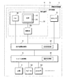
- FIG. 4 is a block diagram illustrating the configuration of the information processing device 1.
- the information processing device 1 includes the above-mentioned optical device 3, an optical device control unit 8, and a system control unit 9.
- the optical device 3 includes a light emitting device 4 and a 3D sensor 6 as described above.
- the optical device control unit 8 controls the optical device 3.
- the optical device control unit 8 includes a shape specifying unit 81.
- the system control unit 9 controls the entire information processing device 1 as a system.
- the system control unit 9 includes an authentication processing unit 91.
- a UI unit 2, a speaker 92, a two-dimensional camera (referred to as a 2D camera in FIG. 2) 93, and the like are connected to the system control unit 9.
- the 3D sensor 6 is an example of a light receiving unit. Hereinafter, they will be described in order.
- the light emitting device 4 included in the optical device 3 includes a light source 10, a widening angle narrowing member 20, a diffuser plate 30, a light receiving element for monitoring the amount of light (referred to as PD in FIG. 2) 40, and a driving unit. It has 50 and.
- the light source 10, the expanding angle narrowing member 20, the diffuser plate 30, and the light receiving element 40 for monitoring the amount of light in the light emitting device 4 will be described later.
- the expanding angle narrowing member 20 is an example of the first optical member
- the diffusion plate 30 is an example of the second optical member.
- the drive unit 50 in the light emitting device 4 drives the light source 10.
- the light source 10 is driven by the drive unit 50 so as to emit light that repeats at several tens of MHz to several hundreds of MHz in a pulsed manner.
- the light emitted by the light source 10 is referred to as an emitted light
- the pulsed light emitted by the light source 10 is referred to as an emitted light pulse.
- the 3D sensor 6 includes a plurality of light receiving regions arranged in a grid pattern.
- the 3D sensor 6 receives the pulsed light reflected from the measurement target in response to the emitted light pulse from the light source 10 of the light emitting device 4.
- the light pulse received by the 3D sensor 6 is referred to as a light receiving pulse.
- the 3D sensor 6 outputs a signal corresponding to the time from when the light is emitted from the light source 10 to when it is reflected by the measurement target and received by the 3D sensor 6 as a digital value for each light receiving region.
- the 3D sensor 6 is configured as a device having a CMOS structure in which each light receiving region has two gates and two charge storage units corresponding to them.
- the 3D sensor 6 may include a lens for condensing light.
- the shape specifying unit 81 of the optical device control unit 8 acquires the digital value obtained for each light receiving region of the 3D sensor 6 from the 3D sensor 6. Then, the shape specifying unit 81 measures the three-dimensional shape of the measurement target by calculating the distance from the acquired digital value to the measurement target for each light receiving region. The shape specifying unit 81 identifies a three-dimensional image from the measured three-dimensional shape.
- the authentication processing unit 91 of the system control unit 9 is the information processing device 1 when the three-dimensional image of the measurement target, which is the specific result specified by the shape identification unit 81, matches the three-dimensional image stored in advance in the ROM or the like. Perform authentication processing related to the use of.
- the authentication process relating to the use of the information processing device 1 is, for example, a process of whether or not to permit the use of the information processing device 1 which is its own device.
- the measurement target is a face
- the information processing device 1 including various applications provided by the information processing device 1 Allow use.
- the shape specifying unit 81 and the authentication processing unit 91 are composed of a CPU that executes a program. Further, these functions may be realized by an integrated circuit such as an ASIC or FPGA. Further, these may be realized by the cooperation between the CPU that executes software such as a program and the integrated circuit.
- the optical device 3, the optical device control unit 8 and the system control unit 9 are shown separately, but the system control unit 9 may include the optical device control unit 8. Further, the optical device control unit 8 may be included in the optical device 3. Further, the optical device 3, the optical device control unit 8 and the system control unit 9 may be integrally configured.
- FIG. 5 is an example of a plan view and a cross-sectional view of the optical device 3 to which the first embodiment is applied.
- 5 (a) is a plan view
- FIG. 5 (b) is a cross-sectional view taken along the line VB-VB of FIG. 5 (a).
- the lateral direction of the paper surface is the x direction
- the upper direction of the paper surface is the y direction
- the surface direction is the z direction.
- the circuit board 7 uses a plate-shaped member made of an insulating material as a base material, and is provided with a conductor pattern made of a conductive material.
- the insulating material is, for example, ceramic or epoxy resin
- the conductive material is, for example, a metal such as copper (Cu) or silver (Ag) or a conductive paste containing these metals.
- the circuit board 7 may be a single-layer substrate having a conductor pattern provided on the surface thereof, or may be a multilayer substrate having a plurality of layers of conductor patterns. Further, the light emitting device 4 and the 3D sensor 6 may be arranged on different circuit boards.
- the light receiving element 40 for monitoring the amount of light, the light source 10, and the driving unit 50 are arranged so as to be arranged in the x direction on the circuit board 7 as an example.
- the spreading angle narrowing member 20 is provided so as to cover the light source 10
- the diffuser plate 30 is provided so as to cover the light source 10 covered with the spreading angle narrowing member 20 and the light intensity monitoring light receiving element 40. There is.
- the light source 10 has a rectangular shape when viewed in a plane.
- the planar shape of the light source 10 does not have to be rectangular.
- the light emitting direction (light emitting side) of the light source 10 is the z direction.
- the light source 10 may be mounted directly on the circuit board 7, or may be mounted on the circuit board 7 via a heat-dissipating base material such as aluminum oxide or aluminum nitride. When passing through the heat radiating base material, the electric power supplied to the light source 10 can be increased to increase the light output of the light source 10.
- the light source 10 will be described as being mounted directly on the circuit board 7.
- the plan view is a shape when viewed in a plan view, and the plan view means a view seen from the z direction in FIG. 5A. The same applies hereinafter.
- the light output means a luminous flux.
- the light source 10 is provided with a vertical resonance type surface emitting laser element (Vertical Cavity Surface Emitting Laser; VCSEL).
- VCSEL Vertical Cavity Surface Emitting Laser
- the vertical resonance type surface emitting laser element is referred to as VCSEL.
- the VCSEL has an active region that serves as a light emitting region between the lower multilayer film reflector and the upper multilayer film reflector laminated on the substrate, and emits laser light in a direction perpendicular to the substrate. ..
- the light source 10 is configured by integrally integrating a plurality of VCSELs as one semiconductor component.
- the number of VCSELs shown in FIG. 5A is an example.
- the VCSEL is an example of a light emitting element.
- the widening angle narrowing member 20 that covers the light source 10 has a light translucency that allows light emitted by a plurality of VCSELs included in the light source 10 (hereinafter referred to as emission light) to pass through, and the emission light of each VCSEL. It is an optical member having a function of narrowing the spreading angle.
- emission light light emitted by a plurality of VCSELs included in the light source 10
- It is an optical member having a function of narrowing the spreading angle.
- a VCSEL emits light from an exit surface, it emits light at a spread angle determined by the structure. That is, as the emitted light is separated from the emitting surface, the irradiation region on the surface parallel to the emitting surface becomes large. Therefore, the spreading angle narrowing member 20 narrows the spreading angle of the light emitted from the VCSEL and emits the light.
- this optical member is referred to as a widening angle narrowing member 20.
- the spread angle refers to an angle range in which the light intensity is 1 / e 2 of the maximum value in the irradiation region on the surface parallel to the exit surface.
- the spread angle of the emitted light may be evaluated by an angle range such as the full width at half maximum (FWHM) of the light intensity.
- the diffusion plate 30 is a member having a rectangular planar shape as an example.
- the diffuser plate 30 diffuses and emits the light incident on the diffuser plate 30.
- the diffuser plate 30 emits light incident on the diffuser plate 30 from the expanding angle narrowing member 20 by changing the directivity. That is, the diffuser plate 30 has a light intensity distribution different from the light intensity distribution when the light emitted from the expanding angle narrowing member 20 (at the time of emission) is irradiated to the irradiation surface 310 without passing through the diffuser plate 30. Light is emitted so as to become.
- the light source 10 can be regarded as a point light source because of its small size as described later.
- the diffusion plate 30 changes the irradiation pattern by the light incident from the light source 10 through the angle narrowing member 20 to the irradiation pattern on the irradiation surface 310 as shown in FIG. 3A.
- the size of the diffusion plate 30 may be, for example, 1 mm to 10 mm in width and length and 0.1 mm to 1 mm in thickness.
- the diffuser plate 30 may cover the light source 10 and the light intensity monitoring light receiving element 40 covered with the expanding angle narrowing member 20 in a plan view. Further, in FIG. 5A, an example in which the shape of the diffusion plate 30 in a plan view is rectangular, but other shapes such as polygons and circles may be used. If the size and shape are as described above, the diffusion plate 30 suitable for face recognition of a portable information processing terminal and measurement of a three-dimensional shape at a relatively short distance up to about several meters is provided.
- the expanding angle narrowing member 20 is held by a support member (not shown) on the z-direction side, which is the light emitting side of the VCSEL included in the light source 10.
- the expanding angle narrowing member 20 is held by a supporting member at a position separated from the emission surface of the VCSEL included in the light source 10 by a predetermined distance.
- the diffuser plate 30 is supported by a side wall 33 on the z-direction side, which is the light emitting side of the light source 10.
- the side wall 33 is provided so as to surround the widening angle narrowing member 20 that covers the light source 10 and the light intensity monitoring light receiving element 40.
- the diffuser plate 30 is held at a predetermined distance from the expanding angle narrowing member 20 covering the light source 10 and the light intensity monitoring light receiving element 40 by the side wall 33. Then, the light that spreads from the light source 10 and enters the diffuser plate 30 through the angle narrowing member 20 is emitted from the diffuser plate 30 and is irradiated to the irradiation surface 310 (see FIG. 2).
- the side wall 33 is composed of a member that absorbs the light emitted by the light source 10, the light emitted by the light source 10 is suppressed from being transmitted to the outside through the side wall 33. Further, by sealing the light source 10, the expanding angle narrowing member 20, and the light receiving element 40 for monitoring the amount of light with the diffusion plate 30 and the side wall 33, dustproof, moistureproof, and the like can be achieved. In the first embodiment, by arranging the light source 10 including the expanding angle narrowing member 20 and the light receiving element 40 for monitoring the amount of light in close proximity to each other, it becomes easy to surround the light source with the side wall 33 having a small size and the diffusion having a small size. The board 30 is sufficient.
- the light amount monitoring light receiving element 40 is a device that outputs an electric signal according to the received light amount (hereinafter, referred to as the light receiving amount).
- the light intensity monitoring light receiving element 40 is a photodiode (PD: Photo Diode) made of, for example, silicon.
- PD Photo Diode
- the light intensity monitoring light receiving element 40 is emitted from the light source 10 via the spreading angle narrowing member 20, and the light reflected on the back surface of the diffuser plate 30, that is, the surface of the diffuser plate 30 on the ⁇ z direction side is received. It is configured.
- the light source 10 is controlled to maintain a predetermined light output based on the light receiving amount of the light amount monitoring light receiving element 40. That is, the optical device control unit 8 controls the light source 10 via the drive unit 50 based on the light reception amount of the light amount monitoring light receiving element 40.
- the optical device control unit 8 suppresses the light output of the light source 10 via the drive unit 50. For example, the optical device control unit 8 stops the emission of light from the light source 10.
- FIG. 6 is an example of a plan view of the light source 10.
- the cathode patterns 71, the anode patterns 72A and 72B, which are conductor patterns provided on the circuit board 7, and the bonding wires 73A and 73B connecting the light source 10 and these conductor patterns are shown together.
- the number of VCSELs shown in FIG. 6 is an example.
- the light source 10 is configured by integrally integrating a plurality of VCSELs.
- a cathode electrode 114 is provided on the back surface of the light source 10 (see FIG. 7 described later), and an anode electrode 118 is provided on the front surface.
- the anode electrode 118 includes a portion for connecting the p-side electrodes 112 of a plurality of VCSELs, a pad portion 118A to which the bonding wire 73A described later is connected, and a pad portion 118B to which the bonding wire 73B is connected. .. That is, the plurality of VCSELs are connected in parallel.
- a plurality of VCSELs in the light source 10 are arranged at each grid point of a grid formed in a square as an example.
- the plurality of VCSELs may be arranged in another arrangement, for example, the positions where the VCSELs are arranged for each row are shifted by half a pitch.
- a cathode pattern 71 and anode patterns 72A and 72B are provided as conductor patterns on the circuit board 7.
- the cathode pattern 71 is formed in an area larger than that of the light source 10 so that the cathode electrode 114 provided on the back surface of the light source 10 is connected. Then, in the light source 10, the cathode electrode 114 provided on the back surface is adhered to the cathode pattern 71 on the circuit board 7 with a conductive adhesive.
- the pad portion 118A of the anode electrode 118 of the light source 10 is connected to the anode pattern 72A on the circuit board 7 by the bonding wire 73A, and the pad portion 118B of the anode electrode 118 of the light source 10 is connected by the bonding wire 73B. It is connected to the anode pattern 72B on the circuit board 7.
- the number of VCSELs included in the light source 10 is, for example, 10 to 1000.
- a plurality of VCSELs constituting the light source 10 are connected in parallel and driven in parallel. That is, the plurality of VCSELs emit light at the same time.
- the light source 10 is, for example, 0.5 mm square to 3 mm square. When irradiating a distant object to be irradiated, the number of VCSELs may be further increased.
- the light source 10 emits light for measuring the three-dimensional shape of the measurement target. In the user authentication based on the face shape described above, the measurement distance is about 10 cm to 1 m. The length of one side of the detection range I is about 1 m.
- the VCSEL constituting the light source 10 is required to have a large light output.
- the light source 10 in which 500 VCSELs are integrated 4 mW to 8 mW is required as the light output of one VCSEL. Therefore, 2W to 4W is required as the light output of the light source 10.
- a VCSEL that oscillates in the multiple transverse mode is used as the VCSEL included in the light source 10.
- Multiple transverse mode is sometimes referred to as multimode. Therefore, the VCSEL that oscillates in the multiple horizontal mode is referred to as a multi-mode VCSEL.
- the single transverse mode may be referred to as a single mode. Therefore, the VCSEL that oscillates in the single transverse mode is referred to as the single mode VCSEL.
- the multi-mode VCSEL has a larger oxide aperture diameter than the single-mode VCSEL, so that the light output is larger. However, the spread angle of the emitted light of the multi-mode VCSEL is larger than that of the single-mode VCSEL.
- the spreading angle narrowing member 20 is provided, the spreading angle of the emitted light of the multimode VCSEL included in the light source 10 is narrowed, and the light is incident on the diffuser plate 30.
- Multi-mode VCSEL (Multiple transverse mode VCSEL (VCSEL-A) with ⁇ resonator structure)
- VCSEL-A Multiple transverse mode VCSEL
- VCSEL-B Single transverse mode VCSEL
- FIG. 7 is a diagram illustrating a cross-sectional structure of a multi-mode VCSEL (VCSEL-A) having a single ⁇ resonator structure constituting the light source 10.
- the upward direction of the paper surface is the z direction.
- VCSEL-A consists of an n-type lower distribution black reflector (DBR: Distributed Bragg Reflector) 102 in which AlGaAs layers having different Al compositions are alternately laminated on a semiconductor substrate 100 such as an n-type GaAs, and an upper spacer layer.
- DBR Distributed Bragg Reflector
- the active region 106 including the quantum well layer sandwiched between the lower spacer layers and the p-type upper distributed black reflector 108 in which AlGaAs layers having different Al compositions are alternately laminated are laminated in this order.
- the distributed black reflector will be referred to as DBR.
- the n-type lower DBR102 is a laminated body in which an Al 0.9 Ga 0.1 As layer and a GaAs layer are paired, and the thickness of each layer is ⁇ / 4 n r (where ⁇ is the oscillation wavelength and n r is the medium). (Refractive index), and these are alternately laminated in 40 cycles.
- the carrier concentration after doping silicon, which is an n-type impurity, is, for example, 3 ⁇ 10 18 cm -3 .
- the active region 106 is configured by laminating a lower spacer layer, a quantum well active layer, and an upper spacer layer.
- the lower spacer layer is an undoped Al 0.6 Ga 0.4 As layer
- the quantum well active layer is an undoped InGaAs quantum well layer and an undoped GaAs barrier layer
- the upper spacer layer is an undoped GaAs barrier layer. It is an Al 0.6 Ga 0.4 As layer.
- the p-type upper DBR108 is a laminated body in which a p-type Al 0.9 Ga 0.1 As layer and a GaAs layer are paired, and the thickness of each layer is ⁇ / 4 nr , and these are alternately used for 29 cycles. It is laminated.
- the carrier concentration after doping with carbon, which is a p-type impurity, is, for example, 3 ⁇ 10 18 cm -3 .
- a contact layer made of p-type GaAs is formed on the uppermost layer of the upper DBR 108, and a current constriction layer 110 of p-type AlAs is formed on the lowermost layer of the upper DBR 108 or inside thereof.
- a columnar mesa M1 is formed on the semiconductor substrate 100 by etching the semiconductor layers laminated from the upper DBR 108 to the lower DBR 102. As a result, the current constriction layer 110 is exposed on the side surface of the mesa M1.
- the current constriction layer 110 is formed with an oxidation region 110A oxidized from the side surface of the mesa M1 and a conductive region 110B surrounded by the oxidation region 110A.
- the AlAs layer has a faster oxidation rate than the AlGaAs layer, and the oxidation region 110A is oxidized from the side surface of the mesa M1 toward the inside at a substantially constant rate.
- the planar shape of the conductive region 110B is changed.
- the shape reflects the outer shape of the mesa M1, that is, a circular shape, and the center thereof substantially coincides with the axial direction of the mesa M1 indicated by the one-point chain line.
- the mesa M1 has a columnar structure.
- the semiconductor layers from the upper DBR 108 to the lower DBR 102 are laminated by epitaxialization. Therefore, this semiconductor layer may be referred to as an epitaxial layer.
- An annular p-side electrode 112 in which Ti / Au or the like is laminated is formed on the uppermost layer of the mesa M1.
- the p-side electrode 112 makes ohmic contact with the contact layer provided on the upper DBR 108.
- the surface of the upper DBR 108 inside the annular p-side electrode 112 serves as a light emission port 112A through which laser light is emitted to the outside. That is, in the VCSEL-A, light is emitted in the direction perpendicular to the semiconductor substrate 100, and the axial direction of the mesa M1 becomes the optical axis.
- a cathode electrode 114 is formed as an n-side electrode on the back surface of the semiconductor substrate 100.
- the surface of the upper DBR 108 inside the p-side electrode 112 is the light emitting surface. That is, the optical axis direction of the VCSEL-A is the light emission direction.
- the insulating layer 116 is provided so as to cover the surface of the mesa M1 except for the portion to which the anode electrode (anode electrode 118 described later) of the p-side electrode 112 is connected and the light emission port 112A. Then, except for the light emission port 112A, the anode electrode 118 is provided so as to make ohmic contact with the p-side electrode 112.
- the anode electrode 118 is commonly provided in a plurality of VCSEL-A. That is, in each of the plurality of VCSEL-A constituting the light source 10, the p-side electrodes 112 are connected in parallel by the anode electrodes 118.
- the anode electrode 118 is provided as a continuous electrode pattern covering the region between each VCSEL-A except for the light emitting port 112A of each VCSEL-A. Therefore, as compared with the case where the drive wiring is individually provided for each VCSEL-A, a pattern having a large area is formed, and the voltage drop when the drive current flows is suppressed.
- FIG. 8 is a diagram schematically illustrating the spread angle ⁇ of the emitted light from the multi-mode VCSEL (VCSEL-A).
- the diffuser plate 30 includes, for example, a glass base material 31 having parallel and flat surfaces on both sides, and a resin layer 32 having a plurality of fine recesses and protrusions formed on one surface of the glass base material 31 to diffuse light. It has.
- the diffuser plate 30 is provided on the path of the emitted light of the VCSEL-A included in the light source 10 (referred to as the light emission path), and the emitted light of the VCSEL-A is diffused and irradiated by the unevenness of the resin layer 32. To do.
- At this time, at least one of the plurality of concave portions and convex portions has a width of 10 ⁇ m or more and 100 ⁇ m or less, and a height (depth) of 1 ⁇ m or more and 50 ⁇ m or less, as an example.
- the plurality of concave portions and convex portions may have a pattern having a period, or may be a random pattern having no period.
- the refraction direction of light is controlled by the patterns of the plurality of concave portions and convex portions, and the light emitted from the light source 10 is shaped into a desired irradiation pattern.
- the pattern of the concave portion and the convex portion may be referred to as a lens pattern.
- the emitted light of the VCSEL-A of the light source 10 has a spreading angle ⁇ .
- the diffuser plate 30 superimposes and irradiates the light emitted by each VCSEL-A.
- FIG. 3A shows the diffuser plate 30 from the light emitted by the light source 10 which can be regarded as a substantially point light source having a side length of 0.5 to 3 mm, for example, by the plurality of concave portions and convex portions formed in the resin layer 32.
- An irradiation pattern having a side length of about 1 m as shown is formed. Since the resin layer 32 of the diffusion plate 30 transmits the light emitted by the VCSEL, the decrease in light utilization efficiency due to absorption is suppressed. Further, since the patterns of the plurality of concave portions and convex portions are easily manufactured by the preformed mold, the light emitting device can be inexpensive.
- FIG. 9 is a diagram illustrating the relationship between the spreading angle ⁇ of the emitted light of the VCSEL-A, the spreading amount of the hem on the irradiation surface 310, and the light utilization efficiency. These relationships were obtained by simulation. As shown in FIG. 9, as the spreading angle ⁇ of the emitted light becomes smaller, the amount of hem spreading on the irradiation surface 310 becomes smaller, and the light utilization efficiency is improved. This is because when the spreading angle of the light emitted from the light source 10 is large, light having various incident angles is incident on the diffuser plate 30 as compared with the case where the spreading angle is small, and the light is refracted by the lens pattern of the diffuser plate 30. The range of corners will be expanded.
- the light of the light source 10 is to reduce the amount of hem spread, that is, to narrow the useless hem range II that is not used for the three-dimensional measurement. Contributes to the improvement of utilization rate. In this way, by narrowing the hem-spreading range II, that is, suppressing the hem-spreading amount, the light utilization efficiency is improved, and the power consumption of the light source 10 is reduced as compared with the case where the hem-spreading amount is not suppressed.
- the spreading angle ⁇ of the emitted light of the VCSEL-A included in the light source 10 is narrowed between the light source 10 and the diffuser plate 30 toward the diffuser plate 30.
- a widening angle narrowing member 20 is provided.
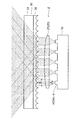
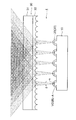
- FIG. 10 is a diagram schematically explaining the relationship between the light source 10 in the light emitting device 4 to which the first embodiment is applied, the convex lens 21 which is an example of the expansion angle narrowing member 20, and the diffusion plate 30.
- the expanding angle narrowing member 20 is a convex lens 21 held between the light source 10 and the diffuser plate 30.
- the convex lens 21 which is an example of the expanding angle narrowing member 20 is referred to as 21 (20). The same shall apply in other cases.
- the light emitted from the VCSEL-A having a spread angle ⁇ incident on the convex lens 21 is emitted from the convex lens 21 at a spread angle ⁇ smaller than the spread angle ⁇ ( ⁇ ⁇ ). That is, the center of the expansion angle ⁇ shifts from the center of the expansion angle ⁇ toward the light source 10.
- the light emitted from the convex lens 21 is shown to be parallel light in all VCSEL-A. In the case of parallel light, ⁇ becomes “0”.
- the light emitted from the convex lens 21 does not have to be parallel light and may be different for each VCSEL-A.
- the action of narrowing the spreading angle differs due to the aberration between the central portion and the peripheral portion of the convex lens 21. Therefore, the spread angle ⁇ is different for each VCSEL-A. Even if the spread angle ⁇ is different for each VCSEL-A, the spread angle ⁇ is narrowed to the spread angle ⁇ by the convex lens 21 and is incident on the diffuser plate 30.
- the convex lens 21 when used as the expansion angle narrowing member 20, the VCSEL-A included in the light source 10 can be regarded as emitting light at an expansion angle ⁇ smaller than the expansion angle ⁇ . Therefore, as shown in FIG. 9, the amount of hem spread on the irradiation surface 310 becomes small.
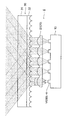
- FIG. 11 is a diagram schematically illustrating the relationship between the light source 10 in the light emitting device 4 to which the first embodiment is applied, the fly-eye lens 22 which is another example of the expansion angle narrowing member 20, and the diffuser plate 30.
- the expanding angle narrowing member 20 is a fly-eye lens 22 held between the light source 10 and the diffuser plate 30.
- the fly-eye lens 22 includes a plurality of convex lenses provided corresponding to each VCSEL-A.
- the fly-eye lens 22 emits the light incident from the VCSEL-A at a spreading angle ⁇ narrower than the spreading angle ⁇ of the light emitted from the VCSEL-A.
- the fly-eye lens 22 is provided corresponding to each VCSEL-A, it becomes easier to control the light emitting direction emitted from the expanding angle narrowing member 20 as compared with the case where the convex lens 21 is used.
- the fly-eye lens 22 is used as the expansion angle narrowing member 20, the VCSEL-A included in the light source 10 can be regarded as emitting light at an expansion angle ⁇ smaller than the expansion angle ⁇ . Therefore, as shown in FIG. 9, the amount of hem spread on the irradiation surface 310 becomes small.
- the fly-eye lens 22 may be configured such that one convex lens corresponds to a plurality of VCSEL-A.
- the convex lens 21 and the fly-eye lens 22 have been described as an example of the expanding angle narrowing member 20.
- the spreading angle narrowing member 20 is not limited to these, and can be applied as long as it is held between the light source 10 and the diffuser plate 30 and narrows the spreading angle of the emitted light of the VCSEL-A.
- the spreading angle narrowing member 20 is held between the light source 10 and the diffuser plate 30 to narrow the spreading angle of the emitted light of the VCSEL-A.
- the expanding angle narrowing member 20 is provided on the light emitting surface of the light source 10. Since the other configurations are the same as those of the first embodiment, the description thereof will be omitted.
- FIG. 12 (a) is a plan view of the optical device 3 to which the second embodiment is applied
- FIG. 12 (b) is a cross-sectional view taken along the line XIIB-XIIB of FIG. 12 (a).
- the lateral direction of the paper surface is the x direction
- the upper direction of the paper surface is the y direction
- the surface direction is the z direction.
- the expanding angle narrowing member 20 is provided on the light source 10 in the light emitting device 4.
- the configuration of the optical device 3 to which the second embodiment is applied is the same as the optical device 3 to which the first embodiment shown in FIG. 5 is applied. Therefore, the same reference numerals are given to the same parts, the description thereof will be omitted, and different parts will be described.
- the expanding angle narrowing member 20 is an array of microlenses 23 and is provided on the VCSEL-A included in the light source 10. ing. Then, individual microlenses 23 are provided corresponding to the respective VCSEL-A. As shown in FIG. 12A, the outer edge of the microlens 23 when viewed in a plan view is circular. If the microlens 23 is provided corresponding to each VCSEL-A, it becomes easy to control the light emitting direction emitted from the expanding angle narrowing member 20.
- the array of microlenses 23 is formed by viscous flow of a photoresist or the like provided on the VCSEL-A by heating. That is, the microlens 23 is formed in the semiconductor manufacturing process for manufacturing the light source 10.
- the microlenses 23 may be connected by the same material as the material constituting the microlens 23.
- the expansion angle narrowing member 20 described in the first embodiment is the fly-eye lens 22
- the light source 10 and the fly-eye lens 22 are configured as separate members, so that the optical device 3 or the light emitting device 4
- the positional relationship between each convex lens of the fly-eye lens 22 and the VCSEL-A included in the light source 10 is mechanically matched. Further, the fly-eye lens 22 may be displaced or detached from the light source 10.
- the expanding angle narrowing member 20 is an array of microlenses 23, since the array of microlenses 23 is formed by the semiconductor manufacturing process, the VCSEL-A and the microlens 23 are compared with the case of the fly-eye lens 22. It is easier to set the positional relationship of. In addition, the array of the microlens 23 is unlikely to come off or shift from the light source 10. Further, the light emitting device 4 becomes smaller by forming the expanding angle narrowing member 20 (array of microlenses 23) on the light source 10.
- FIG. 13 is a diagram schematically explaining the relationship between the light source 10 in the light emitting device 4 to which the second embodiment is applied, the array of the microlens 23 which is an example of the expansion angle narrowing member 20, and the diffuser plate 30. is there.
- the emitted light of the VCSEL-A has a spreading angle ⁇ .
- This emitted light enters the microlens 23 and is emitted as light having a spreading angle ⁇ narrower than the spreading angle ⁇ shown in FIG. 8 ( ⁇ ⁇ ).
- the light emitted from the microlens 23 gradually increases in the irradiation region on the plane perpendicular to the light emission direction as the distance from the VCSEL-A toward the diffuser plate 30, or the size of the irradiation region is constant.
- the light having the spreading angle ⁇ is incident on the diffuser plate 30.
- the VCSEL-A included in the light source 10 can be regarded as emitting light at an expansion angle ⁇ smaller than the expansion angle ⁇ . Therefore, as shown in FIG. 9, the amount of hem spread on the irradiation surface 310 becomes small.
- the microlens 23 may be configured such that one microlens 23 corresponds to a plurality of VCSEL-A.
- the light emitted from the microlens 23 gradually increases in the irradiation region on the plane perpendicular to the light emission direction as the distance from the VCSEL-A toward the diffuser plate 30, or the size of the irradiation region.
- the light emitted from the microlens 23 converges to a certain point in the light emitting direction. May constitute.
- the microlens 23 is configured so as to converge the emitted light, the diameter of the light irradiation region (referred to as the spot diameter) on the diffuser plate 30 becomes smaller, and the uneven pattern provided on the diffuser plate 30 becomes smaller. Can be as large as.
- the diffuser plate 30 is unlikely to form a quadrangular irradiation pattern as shown in FIG. 3A on the irradiation surface 310 unless light is incident on a wide irradiation region including a plurality of concave portions and convex portions. Therefore, the microlens 23 may be configured so as not to converge the light in the light emitting direction of the VCSEL-A.
- the patterns of the plurality of concave portions and convex portions of the diffuser plate 30 are configured so that the amount of hem spreading is the smallest when parallel light is incident as described above. Therefore, the light emitted from the microlens 23 is preferably parallel light, so-called collimated light.
- the parallel light means a case where the spread angle ⁇ is 0 ° or more and 5 ° or less, and it is more preferable that the spread angle ⁇ is 0 ° or more and 2 ° or less.
- the center of the microlens 23, that is, the center of the convex portion is on the optical axis of the VCSEL-A, but even if the center of the microlens 23 is set at a position deviated from the optical axis of the VCSEL-A. Good. As a result, the direction of the light emitted from the microlens 23 deviates from the optical axis direction of the VCSEL-A.
- the VCSEL included in the light source 10 is a multi-mode VCSEL (VCSEL-A) having a ⁇ resonator structure.
- VCSEL-A multi-mode VCSEL
- the multi-mode VCSEL having a ⁇ resonator structure has a larger oxide aperture diameter than the single mode VCSEL having a ⁇ resonator structure, so that a large light output can be obtained.
- the multi-mode VCSEL has a larger spread angle of the emitted light than the single-mode VCSEL. Therefore, if a single-mode VCSEL having a large optical output is used, the spreading angle of the light emitted from the spreading angle narrowing member 20 can be further reduced as compared with the case where the multi-mode VCSEL is used.
- the VCSEL with a long cavity structure has a spacer of several ⁇ to several tens of ⁇ between the active region in the VCSEL of a general ⁇ cavity structure in which the resonator length is the oscillation wavelength ⁇ and one multilayer film reflector.
- the loss in higher-order transverse mode is increased, which enables single-mode oscillation with an oxide aperture diameter larger than the oxidation aperture diameter of VCSEL with a general ⁇ resonator structure. to enable.
- the longitudinal mode interval (sometimes called a free spectrum range) is large, stable operation can be obtained in a single longitudinal mode.
- the longitudinal mode interval becomes narrow due to the increase in the cavity length, and a plurality of standing waves in the longitudinal mode exist in the resonator. Switching between longitudinal modes is more likely to occur.
- the VCSEL having a long resonator structure is provided with a layer that suppresses switching between longitudinal modes (a layer 220 that gives an optical loss in FIG. 14 described below).
- the single-mode VCSEL having a long resonator structure tends to have a narrower spread angle than the single-mode VCSEL having a general ⁇ resonator structure.
- the single transverse mode refers to a mode in which the light intensity distribution of the emitted light with the spread angle as a parameter is monomodal, that is, the light intensity has one peak.
- a mode including a plurality of transverse modes within a range in which monomodality is maintained is also referred to as a single transverse mode.
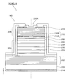
- FIG. 14 is a diagram illustrating a cross-sectional structure of a single-mode VCSEL having a single long resonator structure constituting the light source 10'.
- the single mode VCSEL having a long resonator structure is referred to as VCSEL-B.
- the upward direction of the paper surface is the z direction.
- the VCSEL-B is a resonator extension region formed on an n-type lower DBR202 and a lower DBR202 in which AlGaAs layers having different Al compositions are alternately laminated on an n-type GaAs substrate 200.
- a p-type AlAs current constriction layer 210 is formed in or inside the lowermost layer of the upper DBR208.
- the lower DBR202, the active region 206, the upper DBR208, and the current constriction layer 210 are the same as the lower DBR102, the active region 106, the upper DBR108, and the current constriction layer 110 of the VCSEL-A shown in FIG. 7, and thus the description thereof will be omitted.
- the resonator extension region 204 is a monolithic layer formed by a series of epitaxial growth. Therefore, the resonator extension region 204 is composed of AlGaAs, GaAs, or AlAs so that the lattice constants match or match the GaAs substrate.
- the resonator extension region 204 is made of AlGaAs that does not cause light absorption.
- the film thickness of the resonator extension region 204 is set to 2 ⁇ m to 5 ⁇ m and an oscillation wavelength ⁇ of 5 ⁇ to 20 ⁇ . Therefore, the moving distance of the carrier becomes long.
- the resonator extension region 204 is often n-type with high carrier mobility and is therefore inserted between the n-type lower DBR 202 and the active region 206.
- Such a resonator extension region 204 may be referred to as a cavity extension region or cavity space.
- a carrier block layer 205 having a large band gap for example, made of Al 0.9 Ga 0.1 As, is formed between the resonator extension region 204 and the active region 206. Insertion of the carrier block layer 205 prevents carrier leakage from the active region 206 and improves luminous efficiency. As will be described later, since the layer 220 that gives an optical loss that attenuates the oscillation intensity of the laser beam to some extent is inserted in the resonator extension region 204, the carrier block layer 205 plays a role of compensating for such loss. To bear.
- the thickness of the carrier block layer 205 is ⁇ / 4 mn r (where ⁇ is the oscillation wavelength, m is an integer, and n r is the refractive index of the medium).
- a columnar mesa M2 is formed on the substrate 200 by etching the laminated semiconductor layers from the upper DBR208 to the lower DBR202.
- the current constriction layer 210 is exposed on the side surface of the mesa M2.
- the current constriction layer 210 is formed with an oxidized region 210A selectively oxidized from the side surface of the mesa M2 and a conductive region 210B surrounded by the oxidized region 210A.
- the conductive region 210B is an oxidation aperture.
- the planar shape of the conductive region 210B parallel to the substrate is a shape that reflects the outer shape of the mesa M2, that is, a circular shape, and the center thereof coincides with the axial direction of the mesa M2 indicated by the one-point chain line.
- the diameter of the conductive region 210B for obtaining a single transverse mode (single mode) can be easily increased as compared with the single-mode VCSEL having a normal ⁇ cavity structure.
- the conductive region 210B The diameter of the can be increased from 7 ⁇ m to 8 ⁇ m.
- the semiconductor layers from the upper DBR208 to the lower DBR202 are laminated by epitaxialization. Therefore, this semiconductor layer may be referred to as an epitaxial layer.
- An annular p-side electrode 212 made of metal in which Ti / Au or the like is laminated is formed on the uppermost layer of the mesa M2, and the p-side electrode 212 is ohmic contacted with the contact layer of the upper DBR208.
- the inside of the annular p-side electrode 212 is a light outlet 212A through which laser light is emitted to the outside. That is, the axial direction of the mesa M2 is the optical axis.
- the surface of the upper DBR 108 including the light emission port 212A is the emission surface.
- a cathode electrode 214 is formed as an n-side electrode on the back surface of the substrate 200.
- the insulating layer 216 is provided so as to cover the surface of the mesa M2 except for the portion where the p-side electrode 212 and the anode electrode 218 described later are connected and the light emitting port 212A. Then, except for the light emission port 212A, the anode electrode 218 is provided so as to make ohmic contact with the p-side electrode 212. The anode electrode 218 is provided except for the light emission port 212A of each of the plurality of VCSEL-Bs. That is, in the plurality of VCSEL-Bs included in the light source 10, each p-side electrode 212 is connected in parallel by the anode electrode 218.
- the anode electrode 218 is provided as a continuous electrode pattern covering the region between each VCSEL-B except for the light emitting port 212A of each VCSEL-B. Therefore, as compared with the case where the drive wiring is individually provided for each VCSEL-B, the electrode pattern having a large area is formed, and the voltage drop when the drive current flows is suppressed.
- the required longitudinal mode oscillation wavelength band is set to 940 nm, and in order to suppress switching to the other longitudinal mode oscillation wavelength bands, the unnecessary longitudinal mode standing wave in the resonator extension region 204 is set.
- a layer 220 is provided which provides an optical loss. That is, the layer 220 that provides the optical loss is introduced at the position of the required vertical mode standing wave node.
- the layer 220 that gives an optical loss is made of a semiconductor material having the same Al composition as the semiconductor layer constituting the resonator extension region 204, and is made of, for example, Al 0.3 Ga 0.7 As.
- the layer 220 that gives optical loss preferably has a higher impurity doping concentration than the semiconductor layer that constitutes the cavity extension region 204, and for example, the impurity concentration of AlGaAs that constitutes the resonator extension region 204 is 1 ⁇ 10 17 When it is cm -3 , the layer 220 that gives an optical loss has an impurity concentration of 1 ⁇ 10 18 cm -3 , and is configured to have an impurity concentration about an order of magnitude higher than that of other semiconductor layers. ..
- the film thickness of the layer 220 that provides the optical loss is selected so that the loss to the required longitudinal mode does not increase, and is preferably the same film thickness (10 nm) as the current constriction layer 210 located at the node of the standing wave. ⁇ 30 nm).
- the layer 220 that gives optical loss is inserted so as to be located at the node for the required vertical mode standing wave. Since the light intensity is weak in the standing wave node, the effect of the loss on the required longitudinal mode by the layer 220 that gives the optical loss is small. On the other hand, for unwanted longitudinal mode standing waves, the layer 220, which provides optical loss, is located on the antinode other than the node. Since the antinode of the standing wave has a higher light intensity than the node, the loss given to the unnecessary longitudinal mode by the layer 220 that gives an optical loss becomes large. In this way, by reducing the loss to the required longitudinal mode and increasing the loss to the unnecessary longitudinal mode, the unnecessary longitudinal mode is selectively prevented from resonating, and the longitudinal mode hopping is suppressed.
- the layer 220 that gives the optical loss does not necessarily have to be provided at the position of each node of the required longitudinal mode standing wave in the resonator extension region 204, and may be a single layer. In this case, the intensity of the standing wave increases as it is closer to the active region 206, so that a layer 220 that gives an optical loss at a node position closer to the active region 206 may be formed. Further, if switching or hopping between longitudinal modes is allowed, the layer 220 that causes optical loss may not be provided.
- FIG. 15 is a diagram schematically illustrating the relationship between the light source 10', the microlens 23, which is an example of the spreading angle narrowing member 20, and the diffuser plate 30 in the light emitting device 4 to which the second embodiment is applied. ..
- the expanding angle narrowing member 20 is a microlens 23 provided on the VCSEL-B included in the light source 10'.
- the emitted light of the VCSEL-B has a spreading angle ⁇ smaller than the spreading angle ⁇ shown in FIG. 8 ( ⁇ ⁇ ).
- This emitted light is incident on the microlens 23. It is assumed that the size of the cross section perpendicular to the light emitting direction of the light emitted from the microlens 23 gradually increases or is the same as the distance from the VCSEL-A toward the diffuser plate 30.
- the light emitted from the microlens 23 becomes light having a spreading angle ⁇ narrower than the spreading angle ⁇ shown in FIG. 13 and is incident on the diffuser plate 30 ( ⁇ ⁇ ).
- the expansion angle ⁇ is compared with the case where the light source 10 including VCSEL-A is used. , A small spreading angle ⁇ is emitted from the microlens 23. Therefore, the VCSEL-B included in the light source 10'can be regarded as emitting light at a spreading angle ⁇ smaller than the spreading angle ⁇ . Therefore, as shown in FIG. 9, the amount of hem spread on the irradiation surface 310 becomes small.
- the light emitted from the microlens 23 is preferably parallel light.
- the array of the convex lens 21, the fly-eye lens 22, and the microlens 23 has been described as the expanding angle narrowing member 20. Since these are optical components, it is easy to control the spread angle of the emitted light of the VCSEL, which is a light emitting element.
- the VCSEL which is a light emitting element.
- the three-dimensional shape measurement by the TOF method is required to obtain the light sources 10 and 10'with a large light output.
- the spreading angle narrowing member 20 is used to narrow the spreading angle of the emitted light of the VCSEL included in the light sources 10 and 10'and make it incident on the diffusion plate 30.
- the amount of hem expansion that is, the useless light that spreads by pulling the hem out of the predetermined range (detection range I) on the irradiation surface 310 is suppressed, and the light utilization efficiency is improved.
- the power consumption of the light source is reduced as compared with the case where the amount of hem spread is not suppressed.
- a long drive time is obtained in a battery-powered information processing device such as a portable information processing device.
- a plurality of VCSELs (VCSEL-A, VCSEL-B) are connected in parallel, but a plurality of VCSELs are connected in series. It may be a configuration or a connection form in which a series connection and a parallel connection are combined.
- VCSEL-A, VCSEL-B a plurality of VCSELs
- VCSEL-A, VCSEL-B a plurality of VCSELs
- VCSEL-B a plurality of VCSELs
- a plurality of holes are provided so as to surround the outlet of each VCSEL, and the current constriction layers (current constriction layers 110 and 210) are oxidized using these holes to form a VCSEL having an oxidation constriction structure. You may.
- a plurality of VCSELs are formed from the surface side (surface side) on the substrate 100 on which the epitaxial layer is formed.
- the form of emitting light is shown, the form of emitting light from the surface side (back surface side) on which the epitaxial layer is not formed may be used.
- the light sources 10, 10'and the diffusion plate 30 when viewed from the light emitting surface side, are arranged at overlapping positions. However, it may be in a form arranged at positions where they do not overlap.
- the structure may be such that light can be diffused even at a position where the diffuser plate 30 and the light sources 10 and 10'do not overlap with each other through a reflection member such as a reflection mirror.
- the present application claims priority under Patent Application No. 2019-146382 dated August 8, 2019.
Landscapes
- Engineering & Computer Science (AREA)
- Physics & Mathematics (AREA)
- General Physics & Mathematics (AREA)
- Multimedia (AREA)
- Theoretical Computer Science (AREA)
- General Health & Medical Sciences (AREA)
- Health & Medical Sciences (AREA)
- Computer Vision & Pattern Recognition (AREA)
- Electromagnetism (AREA)
- Optics & Photonics (AREA)
- Oral & Maxillofacial Surgery (AREA)
- Human Computer Interaction (AREA)
- Vascular Medicine (AREA)
- Computer Networks & Wireless Communication (AREA)
- Condensed Matter Physics & Semiconductors (AREA)
- Remote Sensing (AREA)
- Radar, Positioning & Navigation (AREA)
- Signal Processing (AREA)
- Medical Informatics (AREA)
- Software Systems (AREA)
- Evolutionary Computation (AREA)
- Databases & Information Systems (AREA)
- Computing Systems (AREA)
- Artificial Intelligence (AREA)
- Length Measuring Devices By Optical Means (AREA)
- Semiconductor Lasers (AREA)
- Optical Radar Systems And Details Thereof (AREA)
- Optical Elements Other Than Lenses (AREA)
- Stroboscope Apparatuses (AREA)
- Stereoscopic And Panoramic Photography (AREA)
Abstract
光源の発光素子が出射する光の拡がり角を狭めない場合に比べ、予め定められた範囲の外に拡がる裾の部分の光を抑制した発光装置などを提供する。発光装置は、発光素子を複数配列した光源と、光源の光出射経路に設けられ、光源における各発光素子からの出射光の拡がり角を狭くして出射する第1の光学部材と、第1の光学部材の光出射側に設けられ、第1の光学部材側から入射する光を拡散して照射する第2の光学部材と、を備える。
Description
本発明は、発光装置、光学装置及び情報処理装置に関する。
特許文献1には、光源と、所定の平面上において互いに隣接して配置される複数のレンズを有すると共に、光源が出射する光を拡散する拡散板と、拡散板によって拡散された光が被写体で反射した反射光を受光する撮像素子と、を備え、複数のレンズは、拡散された光における干渉縞の周期が三画素以下となるように配置された撮像装置が記載されている。
ところで、タイムオブフライト方式の三次元形状の計測では、計測対象へ光を照射するため、光源から出射された光を拡散させて、予め定められた範囲に、予め定められた光強度分布で照射することが求められる。このとき、予め定められた範囲外にも光が強度を徐々に減衰させながら到達するが、予め定められた範囲外に到達する光は無駄になる。
本発明の目的は、光源の発光素子が出射する光の拡がり角を狭めない場合に比べ、予め定められた範囲の外に到達する光量を抑制した発光装置などを提供する。
本発明の第1態様に係る発光装置は、発光素子を複数配列した光源と、前記光源の光出射経路に設けられ、当該光源における各発光素子からの出射光の拡がり角を狭くして出射する第1の光学部材と、前記第1の光学部材の光出射側に設けられ、当該第1の光学部材側から入射する光を拡散して照射する第2の光学部材と、を備えることを特徴とする。
本発明の第2態様に係る発光装置は、第1態様に係る発光装置において、前記第1の光学部材は、屈折により光の拡がり角を狭くする光学部品であることを特徴とする。
本発明の第3態様に係る発光装置は、第2態様に係る発光装置において、前記第1の光学部材は、前記光源の発光素子上に設けられていることを特徴とする。
本発明の第4態様に係る発光装置は、第3態様に係る発光装置において、前記第1の光学部材は、前記光源の発光素子毎に設けられているマイクロレンズであることを特徴とする。
本発明の第5態様に係る発光装置は、第1態様に係る発光装置において、前記第1の光学部材は、前記光源の各発光素子から入射した光を平行光にして出射することを特徴とする。
本発明の第6態様に係る発光装置は、第1態様に係る発光装置において、前記発光素子は、垂直共振型面発光レーザ素子であることを特徴とする。
本発明の第7態様に係る発光装置は、第6態様に係る発光装置において、前記垂直共振型面発光レーザ素子は、長共振器構造であることを特徴とする。
本発明の第8態様に係る発光装置は、第1~7のいずれかの態様に係る発光装置において、複数の前記発光素子は、電極パターンにより互いに並列に接続されるとともに、当該電極パターンは、各発光素子の出射口を除く領域を、連続したパターンで覆っていることを特徴とする。
本発明の第9態様に係る発光装置は、第1~8のいずれかの態様に係る発光装置において、前記第2の光学部材は、前記第1の光学部材から出射する光の指向性を変えて照射させることを特徴とする。
本発明の第10態様に係る発光装置は、第9態様に係る発光装置において、請求項10に記載の発明は、前記第2の光学部材には、板状の部材であって、少なくとも一方の面に光の指向性を変える構造が設けられていることを特徴とする。
本発明の第11態様に係る発光装置は、第1~9のいずれかの態様に係る発光装置において、前記第2の光学部材は板状の部材であって、少なくとも一方の面に複数の凹部および凸部が設けられていることを特徴とする。
本発明の第12態様に係る発光装置は、第1~11のいずれかの態様に係る発光装置において、前記第2の光学部材は、タイムオブフライト方式による三次元形状の計測に用いる光を照射することを特徴とする。
本発明の第13態様に係る発光装置は、第1~12のいずれかの態様に係る発光装置において、前記光源、前記第1の光学部材及び前記第2の光学部材が携帯型情報処理端末に搭載され、当該光源は前記携帯型情報処理端末の電池によって駆動されることを特徴とする。
本発明の第14態様に係る光源装置は、第1~13のいずれかの態様に係る発光装置と、前記発光装置が備える光源から出射され計測対象で反射された反射光を受光する受光部と、を備え、前記受光部は、前記光源から光が出射されてから当該受光部で受光されるまでの時間に相当する信号を出力することを特徴とする。
本発明の第15態様に係る情報処理装置は、第14態様に係る光学装置と、前記光学装置が備える光源から出射され計測対象で反射され、当該光学装置が備える受光部が受光した反射光に基づき、当該計測対象の三次元形状を特定する形状特定部と、を備えることを特徴とする。
本発明の第16態様に係る情報処理装置は、第15態様に係る情報処理装置において、前記形状特定部での特定結果に基づき、自装置の使用に関する認証処理を行う認証処理部をさらに備えることを特徴とする。
本発明の第2態様に係る発光装置は、第1態様に係る発光装置において、前記第1の光学部材は、屈折により光の拡がり角を狭くする光学部品であることを特徴とする。
本発明の第3態様に係る発光装置は、第2態様に係る発光装置において、前記第1の光学部材は、前記光源の発光素子上に設けられていることを特徴とする。
本発明の第4態様に係る発光装置は、第3態様に係る発光装置において、前記第1の光学部材は、前記光源の発光素子毎に設けられているマイクロレンズであることを特徴とする。
本発明の第5態様に係る発光装置は、第1態様に係る発光装置において、前記第1の光学部材は、前記光源の各発光素子から入射した光を平行光にして出射することを特徴とする。
本発明の第6態様に係る発光装置は、第1態様に係る発光装置において、前記発光素子は、垂直共振型面発光レーザ素子であることを特徴とする。
本発明の第7態様に係る発光装置は、第6態様に係る発光装置において、前記垂直共振型面発光レーザ素子は、長共振器構造であることを特徴とする。
本発明の第8態様に係る発光装置は、第1~7のいずれかの態様に係る発光装置において、複数の前記発光素子は、電極パターンにより互いに並列に接続されるとともに、当該電極パターンは、各発光素子の出射口を除く領域を、連続したパターンで覆っていることを特徴とする。
本発明の第9態様に係る発光装置は、第1~8のいずれかの態様に係る発光装置において、前記第2の光学部材は、前記第1の光学部材から出射する光の指向性を変えて照射させることを特徴とする。
本発明の第10態様に係る発光装置は、第9態様に係る発光装置において、請求項10に記載の発明は、前記第2の光学部材には、板状の部材であって、少なくとも一方の面に光の指向性を変える構造が設けられていることを特徴とする。
本発明の第11態様に係る発光装置は、第1~9のいずれかの態様に係る発光装置において、前記第2の光学部材は板状の部材であって、少なくとも一方の面に複数の凹部および凸部が設けられていることを特徴とする。
本発明の第12態様に係る発光装置は、第1~11のいずれかの態様に係る発光装置において、前記第2の光学部材は、タイムオブフライト方式による三次元形状の計測に用いる光を照射することを特徴とする。
本発明の第13態様に係る発光装置は、第1~12のいずれかの態様に係る発光装置において、前記光源、前記第1の光学部材及び前記第2の光学部材が携帯型情報処理端末に搭載され、当該光源は前記携帯型情報処理端末の電池によって駆動されることを特徴とする。
本発明の第14態様に係る光源装置は、第1~13のいずれかの態様に係る発光装置と、前記発光装置が備える光源から出射され計測対象で反射された反射光を受光する受光部と、を備え、前記受光部は、前記光源から光が出射されてから当該受光部で受光されるまでの時間に相当する信号を出力することを特徴とする。
本発明の第15態様に係る情報処理装置は、第14態様に係る光学装置と、前記光学装置が備える光源から出射され計測対象で反射され、当該光学装置が備える受光部が受光した反射光に基づき、当該計測対象の三次元形状を特定する形状特定部と、を備えることを特徴とする。
本発明の第16態様に係る情報処理装置は、第15態様に係る情報処理装置において、前記形状特定部での特定結果に基づき、自装置の使用に関する認証処理を行う認証処理部をさらに備えることを特徴とする。
本発明の第1態様によれば、光源の発光素子が出射する光の拡がり角を狭めない場合に比べ、予め定められた範囲の外に照射される光量が抑制される。
本発明の第2態様によれば、第1の光学部材が、屈折により光の拡がり角を狭くする光学部品でない場合に比べ、拡がり角の制御が容易にできる。
本発明の第3態様によれば、第1の光学部材を、光源の発光素子上に設けない場合に比べ、発光装置が小型化できる。
本発明の第4態様によれば、マイクロレンズが発光素子毎に設けられていない場合に比べ、光出射方向の制御が容易になる。
本発明の第5態様によれば、第1の光学部材が光源の各発光素子から入射した光を平行光にして出射しない場合に比べ、予め定められた範囲の外に照射される光量がより抑制される。
本発明の第6態様によれば、発光素子が垂直共振型面発光レーザ素子でない場合に比べ、面発光の光源が構成しやすい。
本発明の第7態様によれば、垂直共振型面発光レーザ素子が長共振器構造でない場合に比べ、出射光の拡がり角がより狭くできる。
本発明の第8態様によれば、発光素子毎に配線が設けられる場合に比べ、駆動電流が流れた場合の電圧降下が抑制される。
本発明の第9態様によれば、第2の光学部材が、第1の光学部材から出射する光の指向性を変えない場合に比べ、第1の光学部材側から入射する光を拡散して照射することができる。
本発明の第10態様によれば、板状の部材である第2の光学部材の少なくとも一方の面に光の指向性を変える構造が設けられていない場合に比べ、第1の光学部材側から入射する光を拡散して照射することができる。
本発明の第11態様によれば、板状の部材の少なくとも一方の面に複数の凹部および凸部が設けられた第2の光学部材は容易に製造できるため、発光素子を安価に製造することができる。
本発明の第12態様によれば、タイムオブフライト方式による三次元形状の計測に用いる光の利用効率を高くできる。
本発明の第13態様によれば、光の利用効率を高くできるため、電池の消耗を抑制し、携帯型情報処理端末の駆動時間を長くすることができる。
本発明の第14態様によれば、発光装置によって光が出射されてから受光部によって受光されるまでの時間を計測できる光学装置が提供される。
本発明の第15態様によれば、三次元形状を計測できる情報処理装置が提供される。
本発明の第16態様によれば、三次元形状に基づく認証処理を搭載した情報処理装置が提供される。
本発明の第2態様によれば、第1の光学部材が、屈折により光の拡がり角を狭くする光学部品でない場合に比べ、拡がり角の制御が容易にできる。
本発明の第3態様によれば、第1の光学部材を、光源の発光素子上に設けない場合に比べ、発光装置が小型化できる。
本発明の第4態様によれば、マイクロレンズが発光素子毎に設けられていない場合に比べ、光出射方向の制御が容易になる。
本発明の第5態様によれば、第1の光学部材が光源の各発光素子から入射した光を平行光にして出射しない場合に比べ、予め定められた範囲の外に照射される光量がより抑制される。
本発明の第6態様によれば、発光素子が垂直共振型面発光レーザ素子でない場合に比べ、面発光の光源が構成しやすい。
本発明の第7態様によれば、垂直共振型面発光レーザ素子が長共振器構造でない場合に比べ、出射光の拡がり角がより狭くできる。
本発明の第8態様によれば、発光素子毎に配線が設けられる場合に比べ、駆動電流が流れた場合の電圧降下が抑制される。
本発明の第9態様によれば、第2の光学部材が、第1の光学部材から出射する光の指向性を変えない場合に比べ、第1の光学部材側から入射する光を拡散して照射することができる。
本発明の第10態様によれば、板状の部材である第2の光学部材の少なくとも一方の面に光の指向性を変える構造が設けられていない場合に比べ、第1の光学部材側から入射する光を拡散して照射することができる。
本発明の第11態様によれば、板状の部材の少なくとも一方の面に複数の凹部および凸部が設けられた第2の光学部材は容易に製造できるため、発光素子を安価に製造することができる。
本発明の第12態様によれば、タイムオブフライト方式による三次元形状の計測に用いる光の利用効率を高くできる。
本発明の第13態様によれば、光の利用効率を高くできるため、電池の消耗を抑制し、携帯型情報処理端末の駆動時間を長くすることができる。
本発明の第14態様によれば、発光装置によって光が出射されてから受光部によって受光されるまでの時間を計測できる光学装置が提供される。
本発明の第15態様によれば、三次元形状を計測できる情報処理装置が提供される。
本発明の第16態様によれば、三次元形状に基づく認証処理を搭載した情報処理装置が提供される。
以下、添付図面を参照して、本発明の実施の形態について詳細に説明する。
情報処理装置は、その情報処理装置にアクセスしたユーザがアクセスすることが許可されているか否かを識別し、アクセスが許可されているユーザであることが認証された場合にのみ、自装置である情報処理装置の使用を許可するようになっていることが多い。これまで、パスワード、指紋、虹彩などにより、ユーザを認証する方法が用いられてきた。最近では、さらにセキュリティ性の高い認証方法が求められている。この方法として、ユーザの顔の三次元像による認証が行われるようになっている。
情報処理装置は、その情報処理装置にアクセスしたユーザがアクセスすることが許可されているか否かを識別し、アクセスが許可されているユーザであることが認証された場合にのみ、自装置である情報処理装置の使用を許可するようになっていることが多い。これまで、パスワード、指紋、虹彩などにより、ユーザを認証する方法が用いられてきた。最近では、さらにセキュリティ性の高い認証方法が求められている。この方法として、ユーザの顔の三次元像による認証が行われるようになっている。
ここでは、情報処理装置は、一例として携帯型情報処理端末であるとして説明し、三次元像として捉えられた顔を認識することで、ユーザを認証するとして説明する。なお、情報処理装置は、携帯型情報処理端末以外のパーソナルコンピュータ(PC)などの情報処理装置に適用しうる。
本実施の形態で説明する構成、機能、方法等は、顔の形状による認識以外に、物体の三次元像の取得にも適用しうる。すなわち、顔以外の物体を計測対象として、計測対象の三次元形状を計測して三次元像を取得することに適用してもよい。また、計測対象までの距離(以下では、計測距離と表記する。)は問わない。本実施の形態では、三次元像の取得の対象となる顔や顔以外の物体を、被照射物または被計測物と表記する場合がある。
[第1の実施の形態]
(情報処理装置1)
図1は、第1の実施の形態が適用される情報処理装置1の一例を示す図である。前述したように、情報処理装置1は、一例として携帯型情報処理端末である。
情報処理装置1は、ユーザインターフェイス部(以下では、UI部と表記する。)2と三次元像を取得する光学装置3とを備えている。UI部2は、例えばユーザに対して情報を表示する表示デバイスとユーザの操作により情報処理に対する指示が入力される入力デバイスとが一体化されて構成されている。表示デバイスは、例えば液晶ディスプレイや有機ELディスプレイであり、入力デバイスは、例えばタッチパネルである。
(情報処理装置1)
図1は、第1の実施の形態が適用される情報処理装置1の一例を示す図である。前述したように、情報処理装置1は、一例として携帯型情報処理端末である。
情報処理装置1は、ユーザインターフェイス部(以下では、UI部と表記する。)2と三次元像を取得する光学装置3とを備えている。UI部2は、例えばユーザに対して情報を表示する表示デバイスとユーザの操作により情報処理に対する指示が入力される入力デバイスとが一体化されて構成されている。表示デバイスは、例えば液晶ディスプレイや有機ELディスプレイであり、入力デバイスは、例えばタッチパネルである。
光学装置3は、発光装置4と、三次元センサ(以下では、3Dセンサと表記する。)6とを備えている。発光装置4は、三次元像の取得のために三次元形状を計測する計測対象、ここで説明する例では顔、に向けて光を出射する。3Dセンサ6は、発光装置4が出射した光が顔で反射されて戻ってきた光を取得する。光学装置3は、光の飛行時間による、いわゆるタイムオブフライト(TOF:Time of Flight)方式に基づいて、顔の三次元像を取得する。以下では、計測対象が顔である場合、顔を計測対象と表記することがある。
情報処理装置1は、CPU、ROM、RAMなどを含むコンピュータとして構成されている。ROMには、不揮発性の書き換え可能なメモリ、例えばフラッシュメモリを含む。ROMに蓄積されたプログラムや定数が、RAMに展開される。CPUがRAMに展開されたプログラムを実行することによって、情報処理装置1が動作し、各種の情報処理が実行される。
(情報処理装置1による三次元形状の計測)
図2は、情報処理装置1による三次元形状の計測について説明する図である。ここでの計測対象は、顔300である。図2に図示するように、紙面の右方向をx方向、上方向をz方向とし、紙面の裏面方向をy方向とする。図2は、頭上方向から頭(顔)を見た図である。
図2は、情報処理装置1による三次元形状の計測について説明する図である。ここでの計測対象は、顔300である。図2に図示するように、紙面の右方向をx方向、上方向をz方向とし、紙面の裏面方向をy方向とする。図2は、頭上方向から頭(顔)を見た図である。
情報処理装置1の光学装置3において、発光装置4から光が顔300に向けて出射される。そして、3Dセンサ6により顔300で反射された光が受光される。つまり、光学装置3は、発光装置4から計測対象に向けて光が照射され、3Dセンサ6で計測対象からの反射光が受光されるように構成されている。このとき、発光装置4は、発光装置4に対向して設けられる仮想的な面である照射面310に向けて光を照射する。ここで、発光装置4と照射面310とが正対し、照射面310に立てた垂線321上に発光装置4がある。垂線321は後述する検知範囲Iの中心に立つ。A-A線は、検知範囲Iの中心(垂線321との交点)を通り照射面310をx方向に横切る線である。発光装置4とA-A線上の任意の点とを結ぶ線を線322とする。角度θは、垂線321と線322との間の角度である。
照射面310には、顔300を検知して顔300の三次元形状を計測する検知範囲Iと、検知範囲Iを取り囲む裾引き範囲IIとが形成される。検知範囲Iは、この領域に顔300が存在する場合に、反射光により顔300の三次元形状を計測しうる光強度の光が照射される範囲である。一方、裾引き範囲IIは、検知範囲Iから離れるにしたがい光強度が低下する範囲である。よって、裾引き範囲IIに顔300が存在しても、検知範囲Iに顔300が存在する場合と比べ、顔300の三次元形状は精度よく計測されない。つまり、裾引き範囲IIは、顔300の三次元形状を計測するのに適さない非検知範囲となる。検知範囲I及び裾引き範囲IIは、発光装置4から光が到達する範囲である。そして、検知範囲Iは、三次元形状の計測のために予め定められた範囲であって、予め定められた光強度分布で光が照射される範囲である。ここで、光強度とは、光度を言う。
図3は、照射面310を説明する図である。図3(a)は、照射面310における照射パターンの一例を示す図、図3(b)は、図3(a)のA-A線での光強度分布である。照射面310において光が照射された形状、つまり光が到達した部分の形状を照射パターンと表記する。図3(b)における横軸は、図2に示した垂線321と線322との間の角度θであり、縦軸は、照射面310における光強度である。
図3(a)で示す照射パターンは、x方向に長手方向が向き、角が丸くなった四角形状であるとする。この照射パターンにおいて、中央部の実線で囲んだ長方形の範囲を検知範囲Iに設定し、検知範囲Iの周辺部を裾引き範囲IIとしている。裾引き範囲IIは、検知範囲Iの外側に検知範囲Iを取り巻くように形成されている。なお、検知範囲Iは、長方形状以外の形状に設定されてもよい。
検知範囲Iは、予め定められた光強度分布になるように設定されている。なお、図3(b)では、検知範囲Iは、光強度が一定であるとしているが、予め定められた許容範囲において変動した分布であってもよい。すなわち、被照射物の三次元形状を計測可能な光強度であれば、検知範囲Iの領域内において変動した分布であってもよい。例えば、検知範囲Iにおいて、中央側の方が周辺側より光強度が弱い分布であってもよく、この逆の分布であってもよい。一方、裾引き範囲IIでは、検知範囲Iから離れにつれて、検知範囲Iの光強度から徐々に光強度が低下していく。ここで、裾引き範囲IIにおいて、検知範囲Iと裾引き範囲IIとの境界の角度から、光強度が最大値の1/e2になる角度までの角度差を裾拡がり量とする。裾拡がり量は、裾引き範囲IIの大きさを示す。前述したように、裾引き範囲IIは顔300の三次元形状の計測に適さない領域であり、三次元形状の計測に用いる検知範囲の範囲外となる場合がある。この場合、裾引き範囲IIに照射される光は無効な光となる。よって、裾引き範囲IIの面積が小さいほど、つまり裾拡がり量が小さいほど、発光装置4が出射する光の利用効率(以下では、光利用効率と表記する。)が大きくなる。なお、光利用効率とは、発光装置4が出射する光量の内、検知範囲Iに照射される光量の割合をいう。そして、裾引き範囲IIに照射される光を裾引き光と表記することがある。なお、裾拡がり量を、光強度の半値全幅(FWHM:Full Width at Half Maximum)で評価してもよい。また、裾拡がり量を、角度以外の指標、例えば発光装置4から予め定め設定された距離に置かれた照射面310における裾引き範囲IIの幅などで評価してもよい。
図4は、情報処理装置1の構成を説明するブロック図である。
情報処理装置1は、上記した光学装置3と、光学装置制御部8と、システム制御部9とを備えている。光学装置3は、前述したように発光装置4と3Dセンサ6を備えている。光学装置制御部8は、光学装置3を制御する。そして、光学装置制御部8は、形状特定部81を含む。システム制御部9は、情報処理装置1全体をシステムとして制御する。そして、システム制御部9は、認証処理部91を含む。そして、システム制御部9には、UI部2、スピーカ92、二次元カメラ(図2では、2Dカメラと表記する。)93などが接続されている。なお、3Dセンサ6は、受光部の一例である。
以下、順に説明する。
情報処理装置1は、上記した光学装置3と、光学装置制御部8と、システム制御部9とを備えている。光学装置3は、前述したように発光装置4と3Dセンサ6を備えている。光学装置制御部8は、光学装置3を制御する。そして、光学装置制御部8は、形状特定部81を含む。システム制御部9は、情報処理装置1全体をシステムとして制御する。そして、システム制御部9は、認証処理部91を含む。そして、システム制御部9には、UI部2、スピーカ92、二次元カメラ(図2では、2Dカメラと表記する。)93などが接続されている。なお、3Dセンサ6は、受光部の一例である。
以下、順に説明する。
光学装置3が備えている発光装置4は、光源10と、拡がり角狭化部材20と、拡散板30と、光量監視用受光素子(図2では、PDと表記する。)40と、駆動部50とを備えている。なお、発光装置4における光源10、拡がり角狭化部材20、拡散板30及び光量監視用受光素子40については、後述する。なお、拡がり角狭化部材20は、第1の光学部材の一例、拡散板30は、第2の光学部材の一例である。
発光装置4における駆動部50は、光源10を駆動する。例えば、光源10は、駆動部50により、数10MHz~数100MHzで繰り返す光をパルス状に出射するように駆動される。光源10が出射する光を出射光と表記し、光源10が出射するパルス状の光を、出射光パルスと表記する。
3Dセンサ6は、格子状に配列された複数の受光領域を備えている。3Dセンサ6は、発光装置4の光源10からの出射光パルスに対応して計測対象から反射されたパルス光を受光する。3Dセンサ6が受光する光パルスを受光パルスと表記する。そして、3Dセンサ6は、光源10から光が出射されてから計測対象で反射され3Dセンサ6で受光されるまでの時間に相当する信号を受光領域毎にデジタル値として出力する。例えば、3Dセンサ6は、各受光領域が2つのゲートとそれらに対応した2つの電荷蓄積部を備えたCMOS構造のデバイスとして構成されている。そして、2つのゲートに交互にパルスを加えることによって、各受光領域で発生した光電子を2つの電荷蓄積部の何れかに交互に転送し、出射光パルスと受光パルスとの位相差に応じた電荷を蓄積するように構成されている。そして、ADコンバータを介して、受光領域毎に出射光パルスと受光パルスとの位相差に応じた電荷に対応するデジタル値を信号として出力する。
なお、3Dセンサ6は、集光用のレンズを備えてもよい。
なお、3Dセンサ6は、集光用のレンズを備えてもよい。
光学装置制御部8の形状特定部81は、3Dセンサ6の受光領域毎に得られるデジタル値を3Dセンサ6から取得する。そして、形状特定部81は、取得したデジタル値から受光領域毎に計測対象までの距離を算出することで計測対象の三次元形状を計測する。形状特定部81は、計測した三次元形状から、三次元像を特定する。
システム制御部9の認証処理部91は、形状特定部81により特定された特定結果である計測対象の三次元像がROMなどに予め蓄積された三次元像と一致する場合に、情報処理装置1の使用に関する認証処理を行う。なお、情報処理装置1の使用に関する認証処理とは、一例として、自装置である情報処理装置1の使用を許可するか否かの処理である。計測対象が顔である場合、顔の三次元像がROM等の記憶部材に記憶された顔の三次元像に一致すれば、情報処理装置1が提供する各種アプリケーション等を含む情報処理装置1の使用を許可する。
上記の形状特定部81及び認証処理部91は、一例として、プログラムを実行するCPUによって構成される。また、これらの機能は、ASICやFPGA等の集積回路によって実現されてもよい。さらには、これらは、プログラム等のソフトウエアを実行するCPUと集積回路との協働により実現されてもよい。
また、図4においては、光学装置3、光学装置制御部8及びシステム制御部9をそれぞれ分けて示したが、システム制御部9が光学装置制御部8を含んでもよい。また、光学装置制御部8が光学装置3に含まれてもよい。さらに、光学装置3、光学装置制御部8及びシステム制御部9が一体に構成されてもよい。
また、図4においては、光学装置3、光学装置制御部8及びシステム制御部9をそれぞれ分けて示したが、システム制御部9が光学装置制御部8を含んでもよい。また、光学装置制御部8が光学装置3に含まれてもよい。さらに、光学装置3、光学装置制御部8及びシステム制御部9が一体に構成されてもよい。
(光学装置3の構成)
次に、光学装置3について、詳細に説明する。
図5は、第1の実施の形態が適用される光学装置3の平面図及び断面図の一例である。図5(a)は、平面図、図5(b)は、図5(a)のVB-VB線での断面図である。ここで、図5(a)において、紙面の横方向をx方向、紙面の上方向をy方向とし、表面方向をz方向とする。
次に、光学装置3について、詳細に説明する。
図5は、第1の実施の形態が適用される光学装置3の平面図及び断面図の一例である。図5(a)は、平面図、図5(b)は、図5(a)のVB-VB線での断面図である。ここで、図5(a)において、紙面の横方向をx方向、紙面の上方向をy方向とし、表面方向をz方向とする。
まず、図5(a)に示す平面図を説明する。
光学装置3において、発光装置4と3Dセンサ6とは、一例として回路基板7上にx方向に並ぶように配置されている。回路基板7は、絶縁性材料で構成された板状の部材を基材とし、導電性材料で構成された導体パターンが設けられている。絶縁性材料は、例えばセラミック、エポキシ樹脂などであり、導電性材料は、例えば銅(Cu)、銀(Ag)などの金属又はこれらの金属を含む導電性ペーストである。回路基板7は、導体パターンが表面に設けられた単層基板であってもよく、導体パターンが複数層設けられた多層基板であってもよい。また、発光装置4と3Dセンサ6とは、それぞれが別の回路基板上に配置されていてもよい。
光学装置3において、発光装置4と3Dセンサ6とは、一例として回路基板7上にx方向に並ぶように配置されている。回路基板7は、絶縁性材料で構成された板状の部材を基材とし、導電性材料で構成された導体パターンが設けられている。絶縁性材料は、例えばセラミック、エポキシ樹脂などであり、導電性材料は、例えば銅(Cu)、銀(Ag)などの金属又はこれらの金属を含む導電性ペーストである。回路基板7は、導体パターンが表面に設けられた単層基板であってもよく、導体パターンが複数層設けられた多層基板であってもよい。また、発光装置4と3Dセンサ6とは、それぞれが別の回路基板上に配置されていてもよい。
そして、発光装置4において、光量監視用受光素子40、光源10及び駆動部50は、一例として回路基板7上にx方向に並ぶように配置されている。そして、拡がり角狭化部材20は、光源10を覆うように設けられ、拡散板30は、拡がり角狭化部材20で覆われた光源10及び光量監視用受光素子40を覆うように設けられている。
光源10は、一例として平面視した場合の形状である平面形状が長方形である。なお、光源10の平面形状は、長方形でなくともよい。光源10の光出射方向(光出射側)は、z方向である。なお、光源10は、回路基板7上に直接搭載されてもよいし、酸化アルミニウムや窒化アルミ等の放熱用基材を介して、回路基板7上に搭載されてもよい。放熱用基材を介する場合、光源10に供給する電力を大きくして、光源10の光出力を大きくしうる。以下では、光源10は、回路基板7上に直接搭載されているとして説明する。ここで、平面形状とは、平面視した場合の形状であり、平面視とは、図5(a)において、z方向から見ることをいう。以下同様である。ここで、光出力とは光束をいう。
光源10は、垂直共振型面発光レーザ素子(Vertical Cavity Surface Emitting Laser;VCSEL)を備えている。以下では、垂直共振型面発光レーザ素子をVCSELと表記する。後述するように、VCSELは、基板上に積層された下部多層膜反射鏡と上部多層膜反射鏡との間に発光領域となる活性領域を有し、基板に垂直な方向にレーザ光を出射させる。このことから、VCSELを二次元状に複数配列して、面発光の光源として構成しやすい。光源10は、複数のVCSELが一つの半導体部品として一体集積されて構成されている。なお、図5(a)に示されたVCSELの数は、一例である。そして、VCSELは、発光素子の一例である。
光源10を覆う拡がり角狭化部材20は、光源10が備える複数のVCSELがそれぞれ出射する光(以下では出射光と表記する。)を透過させる光透光性と、それぞれのVCSELの出射光の拡がり角を狭める機能を有する光学部材である。VCSELは、出射面から光を出射する際、構造によって決まる拡がり角で光を出射する。つまり、出射光は、出射面から離れるにつれ、出射面と平行な面における照射領域が大きくなる。そこで、拡がり角狭化部材20は、VCSELの出射光の拡がり角を狭くして出射させる。よって、この光学部材を拡がり角狭化部材20と表記する。ここで、拡がり角は、出射面と平行な面における照射領域において、光強度が最大値の1/e2となる角度範囲を言う。なお、出射光の拡がり角を光強度の半値全幅(FWHM)である角度範囲などで評価してもよい。
拡散板30は、一例として平面形状が長方形の部材である。拡散板30は、拡散板30に入射する光を拡散させて出射する。このとき、拡散板30は、拡がり角狭化部材20から拡散板30に入射する光の指向性を変えて出射する。つまり、拡散板30は、拡がり角狭化部材20から出射される時(出射時)の光が拡散板30を経ずに照射面310に照射された場合における光強度分布と異なる光強度分布となるように光を出射する。例えば、光源10は、後述するようにサイズが小さいため、点光源と見なせる。拡散板30は、光源10から拡がり角狭化部材20を介して入射する光による照射パターンを、図3(a)に示したような照射面310における照射パターンに変える。
拡散板30の大きさは、例えば、横幅及び縦幅が1mm~10mm、厚みは0.1mm~1mmとすればよい。なお、拡散板30は、平面視した状態において、拡がり角狭化部材20で覆われた光源10及び光量監視用受光素子40を覆っていればよい。また、図5(a)では、拡散板30を平面視した形状が長方形である例を示したが、多角形や円形など、他の形状であってもよい。そして、以上のような大きさ及び形状であれば、携帯型情報処理端末の顔認証や、数m程度までの比較的近距離の三次元形状の計測に適した拡散板30が提供される。
次に、図5(b)に示す断面図を説明する。
拡がり角狭化部材20は、光源10が備えるVCSELの光出射側であるz方向側に不図示の支持部材で保持されている。拡がり角狭化部材20は、支持部材により、光源10が備えるVCSELの出射面から予め定められた距離だけ離した位置に保持されている。
拡散板30は、光源10の光出射側であるz方向側に側壁33で支えられている。側壁33は、光源10を覆う拡がり角狭化部材20及び光量監視用受光素子40を囲むように設けられている。拡散板30は、側壁33により光源10を覆う拡がり角狭化部材20及び光量監視用受光素子40から予め定められた距離に保持されている。そして、光源10から拡がり角狭化部材20を介して拡散板30に入射する光は、拡散板30から出射し、照射面310(図2参照)に照射される。
拡がり角狭化部材20は、光源10が備えるVCSELの光出射側であるz方向側に不図示の支持部材で保持されている。拡がり角狭化部材20は、支持部材により、光源10が備えるVCSELの出射面から予め定められた距離だけ離した位置に保持されている。
拡散板30は、光源10の光出射側であるz方向側に側壁33で支えられている。側壁33は、光源10を覆う拡がり角狭化部材20及び光量監視用受光素子40を囲むように設けられている。拡散板30は、側壁33により光源10を覆う拡がり角狭化部材20及び光量監視用受光素子40から予め定められた距離に保持されている。そして、光源10から拡がり角狭化部材20を介して拡散板30に入射する光は、拡散板30から出射し、照射面310(図2参照)に照射される。
側壁33が光源10の出射する光を吸収する部材で構成されていると、光源10が出射する光が側壁33を透過して外部に放射されることが抑制される。また、拡散板30と側壁33とで光源10、拡がり角狭化部材20及び光量監視用受光素子40を封止することで、防塵、防湿等が図られる。第1の実施の形態では、拡がり角狭化部材20を含む光源10と光量監視用受光素子40とを近接して配置することで、小さなサイズの側壁33で囲いやすくなるとともに、小さなサイズの拡散板30で済む。
光量監視用受光素子40は、受光した光量(以下では、受光量と表記する。)に応じた電気信号を出力するデバイスである。光量監視用受光素子40は、例えばシリコンなどで構成されたフォトダイオード(PD:Photo Diode)である。光量監視用受光素子40は、光源10から拡がり角狭化部材20を介して出射され、拡散板30の裏面、つまり拡散板30の-z方向側の面で反射した光が受光されるように構成されている。
光源10は、光量監視用受光素子40の受光量に基づいて、予め定められた光出力を維持するように制御される。つまり、光学装置制御部8は、光量監視用受光素子40の受光量に基づいて、駆動部50を介して光源10を制御する。なお、光量監視用受光素子40の受光量が極端に低下した場合には、拡散板30が外れたり破損したりして、拡がり角狭化部材20を介して光源10の出射する光が拡散板30で拡散されずに直接外部に照射されているおそれがある。このような場合には、光学装置制御部8は、駆動部50を介して光源10の光出力を抑制する。例えば、光学装置制御部8は、光源10からの光の出射を停止させる。
(光源10の構成)
図6は、光源10の平面図の一例である。ここでは、回路基板7上設けられた導体パターンであるカソードパターン71、アノードパターン72A、72B、及び光源10とこれらの導体パターンとを接続するボンディングワイヤ73A、73Bを合わせて示す。なお、図6に示すVCSELの数は、一例である。
図6は、光源10の平面図の一例である。ここでは、回路基板7上設けられた導体パターンであるカソードパターン71、アノードパターン72A、72B、及び光源10とこれらの導体パターンとを接続するボンディングワイヤ73A、73Bを合わせて示す。なお、図6に示すVCSELの数は、一例である。
光源10は、前述したように複数のVCSELが一体集積されて構成されている。そして、光源10の裏面には、カソード電極114が設けられ(後述する図7参照)、表面には、アノード電極118が設けられている。なお、アノード電極118は、複数のVCSELのp側電極112を接続する部分と、後述するボンディングワイヤ73Aが接続されるパッド部118Aと、ボンディングワイヤ73Bが接続されるパッド部118Bとを備えている。つまり、複数のVCSELは、並列接続されている。
図6では、光源10における複数のVCSELは、一例として正方形に組まれた格子の各格子点に配列されている。複数のVCSELは、例えば行毎にVCSELを配置する位置を半ピッチずらした配列など、他の配列で配置してもよい。
回路基板7上には、導体パターンとして、カソードパターン71、アノードパターン72A、72Bが設けられている。カソードパターン71は、光源10の裏面に設けられたカソード電極114が接続されるように、光源10より広い面積で形成されている。そして、光源10は、裏面に設けられたカソード電極114が回路基板7上のカソードパターン71に導電性接着剤にて接着されている。そして、光源10のアノード電極118のパッド部118Aは、ボンディングワイヤ73Aにて、回路基板7上のアノードパターン72Aと接続され、光源10のアノード電極118のパッド部118Bは、ボンディングワイヤ73Bにて、回路基板7上のアノードパターン72Bと接続されている。
光源10が備えるVCSELの数は、例えば、10個~1000個である。光源10を構成する複数のVCSELは、並列に接続され並列駆動される。つまり、複数のVCSELは、同時に光を出射する。光源10は、例えば、0.5mm角~3mm角である。なお、より遠くの被照射物に照射する場合は、さらにVCSELの数を増やしてもよい。
前述したように、光源10は、計測対象の三次元形状を計測するための光を出射する。前述した顔の形状によるユーザの認証では、計測距離は10cm程度から1m程度である。そして、検知範囲Iの一辺長は、1m程度である。光源10としては、検知範囲Iに予め定められた光強度の光を照射することが求められることから、光源10を構成するVCSELは、光出力が大きいことが求められる。一例として、VCSELを500個集積した光源10では、VCSEL一個の光出力として、4mW~8mWが求められる。よって、光源10の光出力として、2W~4Wが求められる。
前述したように、光源10は、計測対象の三次元形状を計測するための光を出射する。前述した顔の形状によるユーザの認証では、計測距離は10cm程度から1m程度である。そして、検知範囲Iの一辺長は、1m程度である。光源10としては、検知範囲Iに予め定められた光強度の光を照射することが求められることから、光源10を構成するVCSELは、光出力が大きいことが求められる。一例として、VCSELを500個集積した光源10では、VCSEL一個の光出力として、4mW~8mWが求められる。よって、光源10の光出力として、2W~4Wが求められる。
第1の実施の形態では、光源10が備えるVCSELとして、多重横モードで発振するVCSELを用いる。多重横モードは、マルチモードと表記されることがある。そこで、多重横モードで発振するVCSELをマルチモードVCSELと表記する。なお、単一横モードは、シングルモードと表記されることがある。よって、単一横モードで発振するVCSELをシングルモードVCSELと表記する。マルチモードVCSELは、シングルモードVCSELに比べて、酸化アパーチャ径を大きく取れるため、光出力が大きくなる。しかし、マルチモードVCSELの出射光の拡がり角は、シングルモードVCSELに比べて大きい。後述するように、拡散板30に入射する光の拡がり角が大きいほど、裾引き範囲IIに照射される光が多くなる。つまり、マルチモードVCSELの出射光を直接拡散板30に入射させると、裾引き範囲IIに照射される無駄な光が多くなる。そこで、第1の実施の形態では、拡がり角狭化部材20を設け、光源10が備えるマルチモードVCSELの出射光の拡がり角を狭くして、拡散板30に入射させる。
(λ共振器構造の多重横モードVCSEL(VCSEL-A))
一例として、第1の実施の形態が適用される光源10が備えるλ共振器構造のマルチモードVCSELを説明する。なお、後述する長共振器構造のシングルモードVCSELと区別するために、λ共振器構造のマルチモードVCSELをVCSEL-Aと表記し、長共振器構造のシングルモードVCSELをVCSEL-Bと表記する。
一例として、第1の実施の形態が適用される光源10が備えるλ共振器構造のマルチモードVCSELを説明する。なお、後述する長共振器構造のシングルモードVCSELと区別するために、λ共振器構造のマルチモードVCSELをVCSEL-Aと表記し、長共振器構造のシングルモードVCSELをVCSEL-Bと表記する。
図7は、光源10を構成する一個のλ共振器構造のマルチモードVCSEL(VCSEL-A)の断面構造を説明する図である。なお、紙面の上方向がz方向である。
VCSEL-Aは、n型のGaAsなどの半導体基板100上に、Al組成の異なるAlGaAs層を交互に重ねたn型の下部分布ブラック型反射鏡(DBR:Distributed Bragg Reflector)102と、上部スペーサ層および下部スペーサ層に挟まれた量子井戸層を含む活性領域106と、Al組成の異なるAlGaAs層を交互に重ねたp型の上部分布ブラック型反射鏡108とが順に積層されて構成されている。以下では、分布ブラック型反射鏡をDBRと表記する。
n型の下部DBR102は、Al0.9Ga0.1As層とGaAs層とをペアとした積層体で、各層の厚さはλ/4nr(但し、λは発振波長、nrは媒質の屈折率)であり、これらを交互に40周期で積層してある。n型不純物であるシリコンをドーピングした後のキャリア濃度は、例えば、3×1018cm-3である。
活性領域106は、下部スペーサ層と、量子井戸活性層と、上部スペーサ層とが積層されて構成されている。例えば、下部スペーサ層は、アンドープのAl0.6Ga0.4As層であり、量子井戸活性層は、アンドープのInGaAs量子井戸層およびアンドープのGaAs障壁層であり、上部スペーサ層は、アンドープのAl0.6Ga0.4As層である。
p型の上部DBR108は、p型のAl0.9Ga0.1As層とGaAs層とをペアとした積層体で、各層の厚さはλ/4nrであり、これらを交互に29周期積層してある。p型不純物であるカーボンをドーピングした後のキャリア濃度は、例えば、3×1018cm-3である。好ましくは、上部DBR108の最上層には、p型GaAsからなるコンタクト層が形成され、上部DBR108の最下層もしくはその内部に、p型AlAsの電流狭窄層110が形成されている。
上部DBR108から下部DBR102に至るまで積層された半導体層をエッチングすることにより、半導体基板100上に円柱状のメサM1が形成される。これにより、電流狭窄層110は、メサM1の側面に露出する。酸化工程により、電流狭窄層110には、メサM1の側面から酸化された酸化領域110Aと酸化領域110Aによって囲まれた導電領域110Bとが形成される。なお、酸化工程において、AlAs層はAlGaAs層よりも酸化速度が速く、酸化領域110Aは、メサM1の側面から内部に向けてほぼ一定の速度で酸化されるため、導電領域110Bの平面形状は、メサM1の外形を反映した形状、すなわち円形状となり、その中心は、一点鎖線で示すメサM1の軸方向とほぼ一致する。メサM1は、柱状構造をなしている。なお、上部DBR108から下部DBR102に至る半導体層は、エピタキシャルにより積層される。よって、この半導体層をエピタキシャル層と表記することがある。
メサM1の最上層には、Ti/Auなどを積層した環状のp側電極112が形成される。p側電極112は、上部DBR108に設けられたコンタクト層にオーミック接触する。環状のp側電極112の内側の上部DBR108の表面は、レーザ光が外部へ出射される光出射口112Aとなる。つまり、VCSEL-Aでは、半導体基板100に垂直な方向に光が出射され、メサM1の軸方向が光軸になる。さらに、半導体基板100の裏面には、n側電極としてカソード電極114が形成される。なお、p側電極112の内側の上部DBR108の表面が光出射面である。つまり、VCSEL-Aの光軸方向が、光出射方向になる。
そして、p側電極112のアノード電極(後述するアノード電極118)が接続される部分および光出射口112Aを除いて、メサM1の表面を覆うように、絶縁層116が設けられる。そして、光出射口112Aを除いて、アノード電極118がp側電極112とオーミック接触するように設けられる。なお、アノード電極118は、複数のVCSEL-Aに共通に設けられている。つまり、光源10を構成する複数のVCSEL-Aは、それぞれのp側電極112がアノード電極118により並列接続されている。このように、アノード電極118は、各VCSEL-Aの光出射口112Aを除く各VCSEL-A間の領域を覆う、連続した電極パターンとして設けられている。このため、VCSEL-A毎に個別に駆動配線を設ける場合と比べ、広い面積のパターンが形成され、駆動電流が流れた場合の電圧降下が抑制される。
(VCSEL-Aの出射光の拡がり角と光強度分布における裾拡がり量との関係)
ここで、拡がり角狭化部材20を用いない場合における光源10が備えるVCSEL-Aの出射光の拡がり角と前述した裾拡がり量との関係を説明する。
図8は、マルチモードVCSEL(VCSEL-A)からの出射光の拡がり角αを模式的に説明する図である。
ここで、拡がり角狭化部材20を用いない場合における光源10が備えるVCSEL-Aの出射光の拡がり角と前述した裾拡がり量との関係を説明する。
図8は、マルチモードVCSEL(VCSEL-A)からの出射光の拡がり角αを模式的に説明する図である。
拡散板30は、例えば、両面が平行で平坦なガラス基材31と、ガラス基材31の一方の表面に光を拡散させるための微細な複数の凹部および凸部が形成された樹脂層32とを備えている。そして、拡散板30は、光源10が備えるVCSEL-Aの出射光の経路(光出射経路と表記する。)上に設けられ、VCSEL-Aの出射光を樹脂層32の凹凸により拡散して照射する。このとき、複数の凹部および凸部の少なくとも一方は、一例として、10μm以上且つ100μm以下の幅を有し、1μm以上且つ50μm以下の高さ(深さ)を有する。また、複数の凹部および凸部は周期を有するパターンであってもよいし、周期を有さないランダムなパターンであってもよい。拡散板30では、この複数の凹部および凸部のパターンにより、光の屈折方向を制御し、光源10から出射された光を所望の照射パターンに整形する。なお、凹部および凸部のパターンは、レンズパターンと呼ばれることがある。ここで、光源10のVCSEL-Aの出射光が拡がり角αである。拡散板30は、各VCSEL-Aが出射する光を重畳して照射する。
拡散板30は、樹脂層32に形成された複数の凹部および凸部により、例えば一辺長が0.5~3mmのほぼ点光源と見なしうる光源10が出射する光から、図3(a)に示したような一辺長が1m程度の照射パターンが形成される。なお、拡散板30の樹脂層32は、VCSELが出射する光を透過するため、吸収による光の利用効率の低下が抑制される。また、複数の凹部および凸部のパターンは、予め形成された型により容易に製造されるため、発光装置を安価にすることができる。
図9は、VCSEL-Aの出射光の拡がり角αと照射面310における裾拡がり量及び光利用効率との関係を説明する図である。これらの関係は、シミュレーションにより求めた。
図9に示すように、出射光の拡がり角αが小さくなるに従い、照射面310における裾拡がり量が小さくなり、光利用効率が向上する。これは、光源10から出射される光の拡がり角が大きいと、拡がり角が小さい場合に比べ、様々な入射角の光が拡散板30へ入射することになり、拡散板30のレンズパターンによる屈折角の範囲が広がることになる。つまり、光源10から出射される光の拡がり角が大きいほど、屈折角が様々な値を取ることになる。すると、拡散板30から照射される光が所望の照射パターンに整形されにくくなり、照射パターンを四角形状とした場合に四角形状がぼやけてしまうことになる。すなわち、光源10から出射される光の拡がり角が大きいほど、裾拡がり量が大きくなる。つまり、拡散板30は、平行光が入射した場合に、最も裾拡がり量が小さくなるように構成されている。
図9に示すように、出射光の拡がり角αが小さくなるに従い、照射面310における裾拡がり量が小さくなり、光利用効率が向上する。これは、光源10から出射される光の拡がり角が大きいと、拡がり角が小さい場合に比べ、様々な入射角の光が拡散板30へ入射することになり、拡散板30のレンズパターンによる屈折角の範囲が広がることになる。つまり、光源10から出射される光の拡がり角が大きいほど、屈折角が様々な値を取ることになる。すると、拡散板30から照射される光が所望の照射パターンに整形されにくくなり、照射パターンを四角形状とした場合に四角形状がぼやけてしまうことになる。すなわち、光源10から出射される光の拡がり角が大きいほど、裾拡がり量が大きくなる。つまり、拡散板30は、平行光が入射した場合に、最も裾拡がり量が小さくなるように構成されている。
光出力が大きい光源10が求められるTOF方式による三次元形状の計測においては、裾拡がり量を小さくする、つまり三次元計測に用いられない無駄な裾引き範囲IIを狭くすることが光源10の光利用率の向上に寄与する。このように、裾引き範囲IIを狭くする、つまり裾拡がり量を抑制することで、光利用効率が向上し、裾拡がり量を抑制しない場合に比べて、光源10の消費電力が低減される。
そこで、第1の実施の形態が適用される発光装置4では、光源10と拡散板30との間に、光源10が備えるVCSEL-Aの出射光の拡がり角αを狭めて拡散板30に向けて出射する拡がり角狭化部材20を設けている。
図10は、第1の実施の形態が適用される発光装置4における光源10、拡がり角狭化部材20の一例である凸レンズ21及び拡散板30の関係を模式的に説明する図である。第1の実施の形態が適用される発光装置4では、拡がり角狭化部材20は、光源10と拡散板30との間に保持された凸レンズ21である。なお、図10では、拡がり角狭化部材20の一例である凸レンズ21を21(20)と表記する。他の場合も同様とする。
凸レンズ21に入射した拡がり角αのVCSEL-Aからの出射光は、拡がり角αより小さい拡がり角βで凸レンズ21から出射する(β<α)。つまり、拡がり角βの中心が拡がり角αの中心から光源10側にずれる。なお、図10では、凸レンズ21から出射した光は、すべてのVCSEL-Aにおいて、平行光であるように図示されている。平行光であればβは、“0”になる。凸レンズ21から出射される光は、平行光でなくともよく、VCSEL-A毎に異なっていてもよい。つまり、光源10のすべてのVCSEL-Aを覆うように設けられた一個の凸レンズ21を用いると、凸レンズ21の中心部と周辺部との収差により拡がり角を狭める作用が異なる。よって、VCSEL-A毎に拡がり角βが異なることになる。VCSEL-A毎に拡がり角βが異なる場合であっても、凸レンズ21により拡がり角αが拡がり角βに狭められて拡散板30に入射する。
上述したように、拡がり角狭化部材20として凸レンズ21を用いると、光源10が備えるVCSEL-Aは、あたかも拡がり角αより小さい拡がり角βで光を出射したと見なせる。よって、図9に示したように、照射面310における裾拡がり量が小さくなる。
図11は、第1の実施の形態が適用される発光装置4における光源10、拡がり角狭化部材20の他の一例であるフライアイレンズ22及び拡散板30の関係を模式的に説明する図である。ここでは、拡がり角狭化部材20は、光源10と拡散板30との間に保持されたフライアイレンズ22である。
フライアイレンズ22は、それぞれのVCSEL-Aに対応して設けられた複数の凸レンズを備えている。フライアイレンズ22は、VCSEL-Aから入射する光をVCSEL-Aの出射光の拡がり角αより狭い拡がり角γで出射する。それぞれのVCSEL-Aに対応してフライアイレンズ22が設けられると、凸レンズ21を用いる場合に比べ、拡がり角狭化部材20から出射する光出射方向の制御が容易になる。
拡がり角狭化部材20としてフライアイレンズ22を用いた場合であっても、光源10が備えるVCSEL-Aは、あたかも拡がり角αより小さい拡がり角γで光を出射したと見なせる。よって、図9に示したように、照射面310における裾拡がり量が小さくなる。なお、フライアイレンズ22は、複数のVCSEL-Aに対して一個の凸レンズが対応するように構成されてもよい。
上記においては、拡がり角狭化部材20の一例として、凸レンズ21及びフライアイレンズ22を説明した。拡がり角狭化部材20は、これらに限らず、光源10と拡散板30との間に保持され、VCSEL-Aの出射光の拡がり角を狭めるものであれば適用されうる。
[第2の実施の形態]
第1の実施の形態では、拡がり角狭化部材20は、光源10と拡散板30との間に保持され、VCSEL-Aの出射光の拡がり角を狭めるものであった。第2の実施の形態が適用される発光装置4では、拡がり角狭化部材20は、光源10の光出射面上に設けられている。なお、他の構成は、第1の実施の形態と同様であるので説明を省略する。
第1の実施の形態では、拡がり角狭化部材20は、光源10と拡散板30との間に保持され、VCSEL-Aの出射光の拡がり角を狭めるものであった。第2の実施の形態が適用される発光装置4では、拡がり角狭化部材20は、光源10の光出射面上に設けられている。なお、他の構成は、第1の実施の形態と同様であるので説明を省略する。
図12(a)は、第2の実施の形態が適用される光学装置3の平面図、図12(b)は、図12(a)のXIIB-XIIB線での断面図である。ここで、図12(a)において、紙面の横方向をx方向、紙面の上方向をy方向とし、表面方向をz方向とする。
図12(a)および図12(b)に示すように、第2の実施の形態が適用される光学装置3では、発光装置4において、拡がり角狭化部材20が光源10上に設けられている。このことを除いて、第2の実施の形態が適用される光学装置3の構成は、図5に示した第1の実施の形態が適用される光学装置3と同じである。よって、同様の部分には同じ符号を付して説明を省略し、異なる部分を説明する。
図12(b)に示すように、第2の実施の形態における発光装置4では、拡がり角狭化部材20は、マイクロレンズ23のアレイであって、光源10が備えるVCSEL-A上に設けられている。そして、個々のマイクロレンズ23がそれぞれのVCSEL-Aに対応して設けられている。なお、図12(a)に示すように、マイクロレンズ23を平面視したときの外縁は、円形となる。それぞれのVCSEL-Aに対応してマイクロレンズ23が設けられると、拡がり角狭化部材20から出射する光出射方向の制御が容易になる。
マイクロレンズ23のアレイは、VCSEL-A上に設けられたフォトレジストなどを加熱により粘性流動させるなどで形成される。つまり、マイクロレンズ23は、光源10を製造する半導体製造プロセスにおいて形成される。なお、マイクロレンズ23間がマイクロレンズ23を構成する材料と同じ材料で連結されていてもよい。
第1の実施の形態で説明した拡がり角狭化部材20がフライアイレンズ22の場合には、光源10とフライアイレンズ22が別の部材として構成されているので、光学装置3又は発光装置4を組み立てる際に、フライアイレンズ22の各凸レンズと光源10が備えるVCSEL-Aとの位置関係を機械的に合わせることになる。また、フライアイレンズ22が光源10に対してずれたり、外れたりするおそれがある。
拡がり角狭化部材20がマイクロレンズ23のアレイの場合には、マイクロレンズ23のアレイが半導体製造プロセスで形成されることから、フライアイレンズ22の場合に比べ、VCSEL-Aとマイクロレンズ23との位置関係がより精密に設定しやすい。また、マイクロレンズ23のアレイが光源10から外れたり、ずれたりしにくい。さらに、光源10上に拡がり角狭化部材20(マイクロレンズ23のアレイ)が形成されることで、発光装置4が小型になる。
拡がり角狭化部材20がマイクロレンズ23のアレイの場合には、マイクロレンズ23のアレイが半導体製造プロセスで形成されることから、フライアイレンズ22の場合に比べ、VCSEL-Aとマイクロレンズ23との位置関係がより精密に設定しやすい。また、マイクロレンズ23のアレイが光源10から外れたり、ずれたりしにくい。さらに、光源10上に拡がり角狭化部材20(マイクロレンズ23のアレイ)が形成されることで、発光装置4が小型になる。
図13は、第2の実施の形態が適用される発光装置4における光源10、拡がり角狭化部材20の一例であるマイクロレンズ23のアレイ及び拡散板30の関係を模式的に説明する図である。
VCSEL-Aの出射光は、拡がり角αである。この出射光がマイクロレンズ23に入射し、図8に示した拡がり角αより狭い拡がり角δの光となって出射する(δ<α)。マイクロレンズ23から出射される光は、VCSEL-Aから拡散板30の方向に離れるに従って、光出射方向に垂直な面における照射領域が徐々に大きくなっていく、又は照射領域の大きさが一定であるとする。この拡がり角δの光が拡散板30に入射する。
拡がり角狭化部材20としてマイクロレンズ23のアレイを用いた場合であっても、光源10が備えるVCSEL-Aは、あたかも拡がり角αより小さい拡がり角δで光を出射したと見なせる。よって、図9に示したように、照射面310における裾拡がり量が小さくなる。なお、マイクロレンズ23は、複数のVCSEL-Aに対して一個が対応するように構成されてもよい。
ここでは、マイクロレンズ23から出射される光は、VCSEL-Aから拡散板30の方向に離れるに従って、光出射方向に垂直な面における照射領域が徐々に大きくなっていく、又は照射領域の大きさが一定であるとした。マイクロレンズ23の表面の曲率やVCSEL-Aの光出射面からマイクロレンズ23の表面までの距離などにより、マイクロレンズ23から出射する光が、光出射方向のある点に収束するようにマイクロレンズ23を構成することがありうる。しかし、出射する光を収束させるようにマイクロレンズ23を構成すると、拡散板30上における光の照射領域の径(スポット径と表記する。)が小さくなり、拡散板30に設けられた凹凸のパターンの大きさと同程度になりうる。拡散板30は、複数の凹部および凸部を含む広い照射領域に光を入射させないと、照射面310において図3(a)に示すような四角形状の照射パターンを形成しにくい。よって、マイクロレンズ23は、VCSEL-Aの光出射方向に光を収束させないように構成することがよい。
そして、拡散板30の複数の凹部および凸部のパターンは、前述したように平行光が入射した場合に、最も裾拡がり量が小さくなるように構成されている。よって、マイクロレンズ23から出射する光は、平行光、いわゆるコリメート光であるとよい。ここでは、平行光とは、拡がり角εが0°以上且つ5°以下である場合を言い、拡がり角εが0°以上且つ2°以下であるとなおよい。なお、このことは、第1の実施の形態における拡がり角狭化部材20である凸レンズ21及びフライアイレンズ22についても同様である。
上記においては、マイクロレンズ23の中心、すなわち凸部の中心がVCSEL-Aの光軸上にあるとしたが、マイクロレンズ23の中心がVCSEL-Aの光軸からずれた位置に設定されてもよい。これにより、マイクロレンズ23から出射する光の向きがVCSEL-Aの光軸方向からずれる。
以上においては、光源10が備えるVCSELは、λ共振器構造のマルチモードVCSEL(VCSEL-A)であるとした。これは、λ共振器構造のマルチモードVCSELは、λ共振器構造のシングルモードVCSELに比べ、酸化アパーチャ径を大きく取れることから、大きな光出力が得られるためであった。しかし、マルチモードVCSELは、シングルモードVCSELに比べ、出射光の拡がり角が大きい。そこで、光出力の大きいシングルモードVCSELを用いれば、マルチモードVCSELを用いる場合に比べ、拡がり角狭化部材20からの出射する光の拡がり角をさらに小さくしうる。
以下では、第2の実施の形態が適用される発光装置4の光源10の変形例として、長共振器構造の単一横モード(シングルモード)VCSELを備えた光源10′を用いた場合を説明する。長共振器構造のVCSELは、共振器長が発振波長λである一般的なλ共振器構造のVCSEL内の活性領域と一方の多層膜反射鏡との間に、数λ~数10λ分のスペーサ層を導入して共振器長を長くすることで高次横モードの損失を増加させ、これにより、一般的なλ共振器構造のVCSELの酸化アパーチャ径よりも大きい酸化アパーチャ径でシングルモード発振を可能にする。典型的なλ共振器構造のVCSELでは、縦モード間隔(フリースペクトルレンジと呼ばれることがある。)が大きいため、単一縦モードで安定的な動作を得ることができる。これに対し、長共振器構造のVCSELの場合には、共振器長が長くなることで縦モード間隔が狭くなり、共振器内に複数の縦モードである定在波が存在し、その結果、縦モード間のスイッチングが起こり易くなる。このため、長共振器構造のVCSELでは、縦モード間のスイッチングを抑制する層(以下で説明する図14における光学的損失を与える層220)を設けている。長共振器構造のシングルモードVCSELは、一般的なλ共振器構造のシングルモードVCSELと比較し、拡がり角をさらに狭くしやすい。なお、単一横モードとは、拡がり角をパラメータとした出射光の光強度分布が単峰性、つまり光強度のピークが1つである特性を有するものを言う。ここでは、単峰性が維持される範囲において複数の横モードを含むものも単一横モードと言う。
(長共振器構造のシングルモードVCSEL(VCSEL-B))
図14は、光源10′を構成する一個の長共振器構造のシングルモードVCSELの断面構造を説明する図である。前述したように、長共振器構造のシングルモードVCSELをVCSEL-Bと表記する。なお、紙面の上方向がz方向である。
VCSEL-Bは、n型のGaAsの基板200上に、Al組成の異なるAlGaAs層を交互に重ねたn型の下部DBR202、下部DBR202上に形成された、共振器長を延長する共振器延長領域204、共振器延長領域204上に形成されたn型のキャリアブロック層205、キャリアブロック層205上に形成された、上部スペーサ層及び下部スペーサ層に挟まれた量子井戸層を含む活性領域206、活性領域206上に形成されたAl組成の異なるAlGaAs層を交互に重ねたp型の上部DBR208を積層して構成されている。なお、上部DBR208の最下層もしくはその内部には、p型AlAsの電流狭窄層210が形成される。
図14は、光源10′を構成する一個の長共振器構造のシングルモードVCSELの断面構造を説明する図である。前述したように、長共振器構造のシングルモードVCSELをVCSEL-Bと表記する。なお、紙面の上方向がz方向である。
VCSEL-Bは、n型のGaAsの基板200上に、Al組成の異なるAlGaAs層を交互に重ねたn型の下部DBR202、下部DBR202上に形成された、共振器長を延長する共振器延長領域204、共振器延長領域204上に形成されたn型のキャリアブロック層205、キャリアブロック層205上に形成された、上部スペーサ層及び下部スペーサ層に挟まれた量子井戸層を含む活性領域206、活性領域206上に形成されたAl組成の異なるAlGaAs層を交互に重ねたp型の上部DBR208を積層して構成されている。なお、上部DBR208の最下層もしくはその内部には、p型AlAsの電流狭窄層210が形成される。
下部DBR202、活性領域206、上部DBR208、電流狭窄層210は、図7で示したVCSEL-Aの下部DBR102、活性領域106、上部DBR108、電流狭窄層110と同じであるので説明を省略する。
共振器延長領域204は、一連のエピタキシャル成長により形成されたモノリシックな層である。従って、共振器延長領域204は、GaAs基板と格子定数が一致し、又は整合するような、AlGaAs、GaAs又はAlAsから構成される。ここでは、940nm帯のレーザ光を出射させるため、共振器延長領域204は、光吸収を生じさせないAlGaAsから構成されている。共振器延長領域204の膜厚は、2μm~5μm、発振波長λの5λ~20λに設定される。このため、キャリアの移動距離が長くなる。よって、共振器延長領域204は、キャリア移動度が大きいn型であることがよく、それゆえn型の下部DBR202と活性領域206との間に挿入される。このような共振器延長領域204は、空洞延長領域又はキャビティスペースと呼ばれることがある。
共振器延長領域204と活性領域206との間に、例えばAl0.9Ga0.1Asからなるバンドギャップの大きいキャリアブロック層205が形成されるとよい。キャリアブロック層205の挿入により、活性領域206からのキャリアリークが防止され、発光効率が改善される。後述するように、共振器延長領域204には、レーザ光の発振強度を幾分減衰させるような光学的損失を与える層220が挿入されるので、キャリアブロック層205は、こうした損失を補填する役割を担う。例えば、キャリアブロック層205の膜厚は、λ/4mnr(但し、λは発振波長、mは整数、nrは媒質の屈折率)である。
上部DBR208から下部DBR202に至るまでの積層された半導体層をエッチングすることにより、基板200上に円柱状のメサM2が形成される。電流狭窄層210は、メサM2の側面に露出する。電流狭窄層210には、メサM2の側面から選択的に酸化された酸化領域210Aと酸化領域210Aによって囲まれた導電領域210Bが形成される。導電領域210Bが、酸化アパーチャである。導電領域210Bの基板と平行な平面形状は、メサM2の外形を反映した形状、すなわち円形状となり、その中心は、一点鎖線で示すメサM2の軸方向と一致する。長共振器構造のシングルモードVCSELでは、単一横モード(シングルモード)を得るための導電領域210Bの径を、通常のλ共振器構造のシングルモードVCSELよりも大きくしやすく、例えば、導電領域210Bの径を7μm~8μmまで大きくしうる。なお、上部DBR208から下部DBR202に至る半導体層は、エピタキシャルにより積層される。よって、この半導体層をエピタキシャル層と表記することがある。
メサM2の最上層には、Ti/Auなどを積層した金属製の環状のp側電極212が形成され、p側電極212は、上部DBR208のコンタクト層にオーミック接触される。環状のp側電極212の内側は、レーザ光が外部へ出射される光出射口212Aとなる。つまり、メサM2の軸方向が光軸になる。なお、光出射口212Aを含む上部DBR108の表面が出射面である。さらに、基板200の裏面には、n側電極としてカソード電極214が形成される。
そして、p側電極212と後述するアノード電極218とが接続される部分及び光出射口212Aを除いて、メサM2の表面を覆うように、絶縁層216が設けられる。そして、光出射口212Aを除いて、アノード電極218がp側電極212とオーミック接触するように設けられる。なお、アノード電極218は、複数のVCSEL-Bのそれぞれの光出射口212Aを除いて設けられる。つまり、光源10に含まれる複数のVCSEL-Bは、それぞれのp側電極212がアノード電極218で並列接続される。このように、アノード電極218は、各VCSEL-Bの光出射口212Aを除く各VCSEL-B間の領域を覆う、連続した電極パターンとして設けられている。このため、VCSEL-B毎に個別に駆動配線を設ける場合と比べ、広い面積の電極パターンが形成され、駆動電流が流れた場合の電圧降下が抑制される。
長共振器構造のシングルモードVCSELでは、共振器長で規定される反射帯域内に複数の縦モードが存在しうるため、縦モード間のスイッチング又はポッピングを抑制する必要がある。ここでは、必要な縦モードの発振波長帯を940nmとし、それ以外の縦モードの発振波長帯へのスイッチングを抑制するべく、共振器延長領域204内に不要な縦モードの定在波に対して光学的損失を与える層220が設けられている。つまり、光学的損失を与える層220は、必要な縦モードの定在波の節の位置に導入されている。光学的損失を与える層220は、共振器延長領域204を構成する半導体層と同じAl組成の半導体材料から構成され、例えば、Al0.3Ga0.7Asから構成されている。光学的損失を与える層220は、好ましくは、共振器延長領域204を構成する半導体層よりも不純物のドーピング濃度が高く、例えば、共振器延長領域204を構成するAlGaAsの不純物濃度が1×1017cm-3であるとき、光学的損失を与える層220は、1×1018cm-3の不純物濃度を有し、他の半導体層よりも1桁程度、不純物濃度が高くなるように構成される。不純物濃度が高くなると、キャリアによる光の吸収が大きくなり、損失が与えられる。光学的損失を与える層220の膜厚は、必要な縦モードへの損失が大きくならないように選択され、好ましくは、定在波の節に位置する電流狭窄層210と同程度の膜厚(10nm~30nm)である。
光学的損失を与える層220は、必要な縦モードの定在波に対しては節に位置するように挿入される。定在波の節では光強度が弱いので、光学的損失を与える層220が必要な縦モードに与える損失の影響は小さい。他方、不要な縦モードの定在波に対しては、光学的損失を与える層220は、節以外の腹に位置する。定在波の腹は節よりも光強度が大きくなるため、光学的損失を与える層220が不要な縦モードに与える損失は大きくなる。こうして、必要な縦モードへの損失を小さくしつつ、不要な縦モードへの損失を大きくすることで、選択的に不要な縦モードが共振されないようにし、縦モードホッピングが抑制される。
光学的損失を与える層220は、共振器延長領域204の必要な縦モードの定在波の各節の位置に必ずしも設けることを要せず、単一の層であってもよい。この場合、定在波の強度は、活性領域206に近いほど大きくなるので、活性領域206から近い節の位置に光学的損失を与える層220を形成すればよい。また、縦モード間のスイッチング又はホッピングが許容されるのであれば、光学的損失を与える層220を設けなくてもよい。
図15は、第2の実施の形態が適用される発光装置4における光源10′、拡がり角狭化部材20の一例であるマイクロレンズ23及び拡散板30の関係を模式的に説明する図である。第2の実施の形態が適用される発光装置4では、拡がり角狭化部材20は、光源10′が備えるVCSEL-B上に設けられたマイクロレンズ23である。
VCSEL-Bの出射光は、図8に示した拡がり角αより小さい拡がり角εである(ε<α)。この出射光がマイクロレンズ23に入射する。マイクロレンズ23から出射される光は、VCSEL-Aから拡散板30の方向に離れるに従って、光出射方向に垂直な断面の大きさが徐々に大きくなっていく、又は同じであるとする。このマイクロレンズ23から出射する光は、図13に示した拡がり角δより狭い拡がり角ζの光となり、拡散板30に入射する(ζ<δ)。
拡がり角狭化部材20としてマイクロレンズ23のアレイを用いた場合であっても、VCSEL-Bを備える光源10′を用いると、VCSEL-Aを備える光源10を用いた場合の拡がり角δに比べ、小さい拡がり角ζとなってマイクロレンズ23から出射される。よって、光源10′が備えるVCSEL-Bは、あたかも拡がり角εより小さい拡がり角ζで光を出射したと見なせる。よって、図9に示したように、照射面310における裾拡がり量が小さくなる。なお、前述したように、マイクロレンズ23から出射される光は、平行光であるとよい。
第1の実施の形態及び第2の実施の形態で説明したように、拡がり角狭化部材20として凸レンズ21、フライアイレンズ22、マイクロレンズ23のアレイを説明した。これらは、光学部品であることから、発光素子であるVCSELの出射光の拡がり角の制御が容易である。
ここでは、拡散板30に入射する光の拡がり角が小さいほどと照射面310における裾拡がり量が小さくなることから、光出力が大きい光源10、10′が求められるTOF方式による三次元形状の計測において、拡がり角狭化部材20を用いて、光源10、10′が備えるVCSELの出射光の拡がり角を狭めて拡散板30に入射させている。これにより、裾拡がり量、つまり照射面310において予め定められた範囲(検知範囲I)外に裾を引いて拡がる無駄な光を抑制し、光利用効率を向上させている。このようにすることで、裾拡がり量を抑制しない場合に比べて、光源の消費電力を低減させている。特に、携帯型情報処理装置など、電池で駆動される情報処理装置において長い駆動時間が得られている。
ここでは、拡散板30に入射する光の拡がり角が小さいほどと照射面310における裾拡がり量が小さくなることから、光出力が大きい光源10、10′が求められるTOF方式による三次元形状の計測において、拡がり角狭化部材20を用いて、光源10、10′が備えるVCSELの出射光の拡がり角を狭めて拡散板30に入射させている。これにより、裾拡がり量、つまり照射面310において予め定められた範囲(検知範囲I)外に裾を引いて拡がる無駄な光を抑制し、光利用効率を向上させている。このようにすることで、裾拡がり量を抑制しない場合に比べて、光源の消費電力を低減させている。特に、携帯型情報処理装置など、電池で駆動される情報処理装置において長い駆動時間が得られている。
なお、上記の第1の実施の形態及び第2の実施の形態では、複数のVCSEL(VCSEL-A、VCSEL-B)が並列接続される例を示したが、複数のVCSELが直列接続される構成や、直列接続と並列接続とを組み合わせた接続形態であってもよい。
また、上記の第1の実施の形態及び第2の実施の形態では、複数のVCSEL(VCSEL-A、VCSEL-B)がメサ形状で構成される例を示したが、メサ形状以外の形態であってもよい。例えば、各VCSELの出射口の周囲を取り囲むように複数の孔を設け、この孔を利用して電流狭窄層(電流狭窄層110、210)を酸化することで、酸化狭窄構造を有するVCSELを構成してもよい。
また、上記の第1の実施の形態及び第2の実施の形態では、複数のVCSEL(VCSEL-A、VCSEL-B)が、基板100上のエピタキシャル層が形成された面側(表面側)から光を出射する形態を示したが、エピタキシャル層が形成されていない面側(裏面側)から光を出射する形態であってもよい。
また、上記の第1の実施の形態及び第2の実施の形態では、光の出射面側から見た場合に、光源10、10′と拡散板30とが重なる位置に配置された形態を示したが、重ならない位置に配置された形態であってもよい。例えば、反射ミラー等の反射部材を介することで、拡散板30と光源10、10′とが重ならない位置であっても、光を拡散できる構成であればよい。
本願は、2019年8月8日付の特許願弟2019-146382号に基づき優先権を主張する。
本願は、2019年8月8日付の特許願弟2019-146382号に基づき優先権を主張する。
Claims (16)
- 発光素子を複数配列した光源と、
前記光源の光出射経路に設けられ、当該光源における各発光素子からの出射光の拡がり角を狭くして出射する第1の光学部材と、
前記第1の光学部材の光出射側に設けられ、当該第1の光学部材側から入射する光を拡散して照射する第2の光学部材と、を備える発光装置。 - 前記第1の光学部材は、屈折により光の拡がり角を狭くする光学部品である請求項1に記載の発光装置。
- 前記第1の光学部材は、前記光源の発光素子上に設けられている請求項1または2に記載の発光装置。
- 前記第1の光学部材は、前記光源の発光素子毎に設けられているマイクロレンズである請求項1~3のいずれか一項に記載の発光装置。
- 前記第1の光学部材は、前記光源の各発光素子から入射した光を平行光にして出射する請求項1~4のいずれか一項に記載の発光装置。
- 前記発光素子は、垂直共振型面発光レーザ素子である請求項1~4のいずれか一項に記載の発光装置。
- 前記垂直共振型面発光レーザ素子は、長共振器構造である請求項6に記載の発光装置。
- 複数の前記発光素子は、電極パターンにより互いに並列に接続されるとともに、当該電極パターンは、各発光素子の出射口を除く領域を、連続したパターンで覆っている請求項1ないし7のいずれか1項に記載の発光装置。
- 前記第2の光学部材は、前記第1の光学部材から出射する光の指向性を変えて照射させる請求項1ないし8のいずれか1項に記載の発光装置。
- 前記第2の光学部材は、板状の部材であって、少なくとも一方の面に光の指向性を変える構造が設けられている請求項9に記載の発光装置。
- 前記第2の光学部材は板状の部材であって、少なくとも一方の面に複数の凹部および凸部が設けられている請求項1ないし9のいずれか1項に記載の発光装置。
- 前記第2の光学部材は、タイムオブフライト方式による三次元形状の計測に用いる光を照射する請求項1ないし11のいずれか1項に記載の発光装置。
- 前記光源、前記第1の光学部材及び前記第2の光学部材が携帯型情報処理端末に搭載され、当該光源は前記携帯型情報処理端末の電池によって駆動される請求項1ないし12のいずれか1項に記載の発光装置。
- 請求項1ないし13のいずれか1項に記載の発光装置と、
前記発光装置が備える光源から出射され計測対象で反射された反射光を受光する受光部と、を備え、
前記受光部は、前記光源から光が出射されてから当該受光部で受光されるまでの時間に相当する信号を出力する光学装置。 - 請求項14に記載の光学装置と、
前記光学装置が備える光源から出射され計測対象で反射され、当該光学装置が備える受光部が受光した反射光に基づき、当該計測対象の三次元形状を特定する形状特定部と、を備える情報処理装置。 - 前記形状特定部での特定結果に基づき、自装置の使用に関する認証処理を行う認証処理部、をさらに備える請求項15に記載の情報処理装置。
Priority Applications (1)
| Application Number | Priority Date | Filing Date | Title |
|---|---|---|---|
| US17/559,626 US20220114835A1 (en) | 2019-08-08 | 2021-12-22 | Light-emitting device, optical device, and information processing device |
Applications Claiming Priority (2)
| Application Number | Priority Date | Filing Date | Title |
|---|---|---|---|
| JP2019146382A JP2021025965A (ja) | 2019-08-08 | 2019-08-08 | 発光装置、光学装置及び情報処理装置 |
| JP2019-146382 | 2019-08-08 |
Related Child Applications (1)
| Application Number | Title | Priority Date | Filing Date |
|---|---|---|---|
| US17/559,626 Continuation US20220114835A1 (en) | 2019-08-08 | 2021-12-22 | Light-emitting device, optical device, and information processing device |
Publications (1)
| Publication Number | Publication Date |
|---|---|
| WO2021024508A1 true WO2021024508A1 (ja) | 2021-02-11 |
Family
ID=74502569
Family Applications (1)
| Application Number | Title | Priority Date | Filing Date |
|---|---|---|---|
| PCT/JP2019/048789 Ceased WO2021024508A1 (ja) | 2019-08-08 | 2019-12-12 | 発光装置、光学装置及び情報処理装置 |
Country Status (3)
| Country | Link |
|---|---|
| US (1) | US20220114835A1 (ja) |
| JP (1) | JP2021025965A (ja) |
| WO (1) | WO2021024508A1 (ja) |
Cited By (4)
| Publication number | Priority date | Publication date | Assignee | Title |
|---|---|---|---|---|
| WO2022201772A1 (ja) * | 2021-03-23 | 2022-09-29 | ソニーセミコンダクタソリューションズ株式会社 | 面発光レーザ、光源装置、電子機器及び面発光レーザの製造方法 |
| WO2023026536A1 (ja) * | 2021-08-26 | 2023-03-02 | ソニーグループ株式会社 | 面発光素子及び面発光素子の製造方法 |
| WO2023058353A1 (ja) * | 2021-10-07 | 2023-04-13 | ソニーセミコンダクタソリューションズ株式会社 | 発光装置、発光装置の製造方法、および測距装置 |
| WO2024195323A1 (ja) * | 2023-03-17 | 2024-09-26 | ソニーセミコンダクタソリューションズ株式会社 | 発光装置、及び測距システム |
Families Citing this family (4)
| Publication number | Priority date | Publication date | Assignee | Title |
|---|---|---|---|---|
| JP2021048206A (ja) * | 2019-09-18 | 2021-03-25 | ソニーセミコンダクタソリューションズ株式会社 | 半導体レーザ駆動装置、電子機器、および、半導体レーザ駆動装置の製造方法 |
| EP4321903A4 (en) * | 2021-04-08 | 2024-10-09 | Hesai Technology Co., Ltd. | SOLID-STATE LASER RADAR AND METHOD FOR DETECTION USING THE SAME |
| US20240302581A1 (en) * | 2023-03-09 | 2024-09-12 | Ii-Vi Delaware, Inc. | Systems and methods for an ultra-wide field of illumination diffuser |
| JP2026003323A (ja) * | 2024-06-24 | 2026-01-13 | スタンレー電気株式会社 | 発光モジュール |
Citations (8)
| Publication number | Priority date | Publication date | Assignee | Title |
|---|---|---|---|---|
| JP2003158332A (ja) * | 2001-09-10 | 2003-05-30 | Fuji Photo Film Co Ltd | レーザーダイオードアレイ、レーザー装置、合波レーザー光源および露光装置 |
| JP2007214564A (ja) * | 2006-02-06 | 2007-08-23 | Avago Technologies General Ip (Singapore) Private Ltd | 面発光レーザ(vcsel)アレイ・レーザスキャナ |
| JP2007533962A (ja) * | 2003-09-18 | 2007-11-22 | ライカ ジオシステムズ アクチェンゲゼルシャフト | レーザー光源を備える測地線装置 |
| JP2009204691A (ja) * | 2008-02-26 | 2009-09-10 | Toyota Central R&D Labs Inc | 光走査装置、レーザレーダ装置、及び光走査方法 |
| US20140240469A1 (en) * | 2013-02-28 | 2014-08-28 | Motorola Mobility Llc | Electronic Device with Multiview Image Capture and Depth Sensing |
| JP2015144299A (ja) * | 2006-08-23 | 2015-08-06 | 株式会社リコー | 面発光レーザアレイ、それを備えた光走査装置および画像形成装置 |
| JP2016213486A (ja) * | 2016-07-14 | 2016-12-15 | 富士ゼロックス株式会社 | 面発光型半導体レーザ、面発光型半導体レーザ装置、光伝送装置および情報処理装置 |
| JP2019096642A (ja) * | 2017-11-17 | 2019-06-20 | シャープ株式会社 | 発光素子駆動回路、および携帯型電子機器 |
Family Cites Families (11)
| Publication number | Priority date | Publication date | Assignee | Title |
|---|---|---|---|---|
| KR20110007456A (ko) * | 2009-07-16 | 2011-01-24 | 주식회사 엑스엘 | 광 모듈 및 그 제조방법 |
| US20110187878A1 (en) * | 2010-02-02 | 2011-08-04 | Primesense Ltd. | Synchronization of projected illumination with rolling shutter of image sensor |
| US9407837B2 (en) * | 2013-02-28 | 2016-08-02 | Google Inc. | Depth sensor using modulated light projector and image sensor with color and IR sensing |
| US20150260830A1 (en) * | 2013-07-12 | 2015-09-17 | Princeton Optronics Inc. | 2-D Planar VCSEL Source for 3-D Imaging |
| US9918073B2 (en) * | 2014-12-22 | 2018-03-13 | Google Llc | Integrated camera system having two dimensional image capture and three dimensional time-of-flight capture with movable illuminated region of interest |
| US9798126B2 (en) * | 2015-08-25 | 2017-10-24 | Rockwell Automation Technologies, Inc. | Modular illuminator for extremely wide field of view |
| CN108779905B (zh) * | 2016-01-26 | 2021-08-20 | 新加坡恒立私人有限公司 | 多模式照明模块和相关方法 |
| US10334184B2 (en) * | 2016-09-16 | 2019-06-25 | Apple Inc. | Electronic device with light diffuser |
| US10481269B2 (en) * | 2017-12-07 | 2019-11-19 | Ouster, Inc. | Rotating compact light ranging system |
| JP7238343B2 (ja) * | 2017-12-22 | 2023-03-14 | 株式会社デンソー | 距離測定装置及び距離測定方法 |
| US11397077B2 (en) * | 2018-01-05 | 2022-07-26 | Stmicroelectronics, Inc. | Power and security adjustment for face identification with reflectivity detection by a ranging sensor |
-
2019
- 2019-08-08 JP JP2019146382A patent/JP2021025965A/ja active Pending
- 2019-12-12 WO PCT/JP2019/048789 patent/WO2021024508A1/ja not_active Ceased
-
2021
- 2021-12-22 US US17/559,626 patent/US20220114835A1/en not_active Abandoned
Patent Citations (8)
| Publication number | Priority date | Publication date | Assignee | Title |
|---|---|---|---|---|
| JP2003158332A (ja) * | 2001-09-10 | 2003-05-30 | Fuji Photo Film Co Ltd | レーザーダイオードアレイ、レーザー装置、合波レーザー光源および露光装置 |
| JP2007533962A (ja) * | 2003-09-18 | 2007-11-22 | ライカ ジオシステムズ アクチェンゲゼルシャフト | レーザー光源を備える測地線装置 |
| JP2007214564A (ja) * | 2006-02-06 | 2007-08-23 | Avago Technologies General Ip (Singapore) Private Ltd | 面発光レーザ(vcsel)アレイ・レーザスキャナ |
| JP2015144299A (ja) * | 2006-08-23 | 2015-08-06 | 株式会社リコー | 面発光レーザアレイ、それを備えた光走査装置および画像形成装置 |
| JP2009204691A (ja) * | 2008-02-26 | 2009-09-10 | Toyota Central R&D Labs Inc | 光走査装置、レーザレーダ装置、及び光走査方法 |
| US20140240469A1 (en) * | 2013-02-28 | 2014-08-28 | Motorola Mobility Llc | Electronic Device with Multiview Image Capture and Depth Sensing |
| JP2016213486A (ja) * | 2016-07-14 | 2016-12-15 | 富士ゼロックス株式会社 | 面発光型半導体レーザ、面発光型半導体レーザ装置、光伝送装置および情報処理装置 |
| JP2019096642A (ja) * | 2017-11-17 | 2019-06-20 | シャープ株式会社 | 発光素子駆動回路、および携帯型電子機器 |
Cited By (5)
| Publication number | Priority date | Publication date | Assignee | Title |
|---|---|---|---|---|
| WO2022201772A1 (ja) * | 2021-03-23 | 2022-09-29 | ソニーセミコンダクタソリューションズ株式会社 | 面発光レーザ、光源装置、電子機器及び面発光レーザの製造方法 |
| WO2023026536A1 (ja) * | 2021-08-26 | 2023-03-02 | ソニーグループ株式会社 | 面発光素子及び面発光素子の製造方法 |
| EP4391253A4 (en) * | 2021-08-26 | 2025-01-15 | Sony Group Corporation | SURFACE LIGHT-EMITTING ELEMENT AND METHOD FOR PRODUCING THE SURFACE LIGHT-EMITTING ELEMENT |
| WO2023058353A1 (ja) * | 2021-10-07 | 2023-04-13 | ソニーセミコンダクタソリューションズ株式会社 | 発光装置、発光装置の製造方法、および測距装置 |
| WO2024195323A1 (ja) * | 2023-03-17 | 2024-09-26 | ソニーセミコンダクタソリューションズ株式会社 | 発光装置、及び測距システム |
Also Published As
| Publication number | Publication date |
|---|---|
| US20220114835A1 (en) | 2022-04-14 |
| JP2021025965A (ja) | 2021-02-22 |
Similar Documents
| Publication | Publication Date | Title |
|---|---|---|
| JP2021025965A (ja) | 発光装置、光学装置及び情報処理装置 | |
| CN113574682B (zh) | 发光装置、光学装置以及信息处理装置 | |
| JP6763452B1 (ja) | 発光装置、光学装置および情報処理装置 | |
| JP7334439B2 (ja) | 垂直共振器面発光レーザ素子アレイチップ、発光装置、光学装置および情報処理装置 | |
| KR20190040832A (ko) | 광원 일체형 광 센싱 시스템 및 이를 포함하는 전자 기기 | |
| US11605936B2 (en) | Light-emitting device, optical device, and information processing apparatus | |
| JP2020155622A (ja) | 発光装置、光学装置および情報処理装置 | |
| US11539191B2 (en) | Light-emitting device, optical device, and information processing apparatus | |
| US20220115836A1 (en) | Light-emitting device, optical device, and information processing device | |
| US11599610B2 (en) | Light-emitting device, optical device, and information processing apparatus | |
| US20190221997A1 (en) | Power monitoring approach for vcsels and vcsel arrays | |
| US12388232B2 (en) | Light-emitting device, optical device, measurement device, and information processing apparatus | |
| US12567723B2 (en) | Light-emitting device, optical device, and information processing device | |
| US12261414B2 (en) | Light-emission device, optical device, and information processing device | |
| US20220003874A1 (en) | Light-emitting device, optical device, and information processing device | |
| JP7413655B2 (ja) | 発光装置及び情報処理装置 | |
| WO2020188837A1 (ja) | 発光装置、光学装置および情報処理装置 | |
| US12057677B2 (en) | Light-emitting device, optical device, and information processing apparatus | |
| JP7413657B2 (ja) | 光学装置及び情報処理装置 |
Legal Events
| Date | Code | Title | Description |
|---|---|---|---|
| 121 | Ep: the epo has been informed by wipo that ep was designated in this application |
Ref document number: 19940951 Country of ref document: EP Kind code of ref document: A1 |
|
| NENP | Non-entry into the national phase |
Ref country code: DE |
|
| 122 | Ep: pct application non-entry in european phase |
Ref document number: 19940951 Country of ref document: EP Kind code of ref document: A1 |