WO2021020344A1 - Photosensitive resin composition, photosensitive sheet, cured film, method for producing cured film, interlayer insulating film and electronic component - Google Patents
Photosensitive resin composition, photosensitive sheet, cured film, method for producing cured film, interlayer insulating film and electronic component Download PDFInfo
- Publication number
- WO2021020344A1 WO2021020344A1 PCT/JP2020/028701 JP2020028701W WO2021020344A1 WO 2021020344 A1 WO2021020344 A1 WO 2021020344A1 JP 2020028701 W JP2020028701 W JP 2020028701W WO 2021020344 A1 WO2021020344 A1 WO 2021020344A1
- Authority
- WO
- WIPO (PCT)
- Prior art keywords
- general formula
- photosensitive resin
- group
- resin composition
- indicates
- Prior art date
Links
- 239000011342 resin composition Substances 0.000 title claims abstract description 62
- 238000004519 manufacturing process Methods 0.000 title claims description 8
- 239000011229 interlayer Substances 0.000 title claims description 7
- -1 alicyclic hydrocarbon Chemical class 0.000 claims abstract description 120
- 229920001721 polyimide Polymers 0.000 claims abstract description 30
- 239000004642 Polyimide Substances 0.000 claims abstract description 28
- 239000002243 precursor Substances 0.000 claims abstract description 25
- 125000004435 hydrogen atom Chemical group [H]* 0.000 claims abstract description 21
- 125000004432 carbon atom Chemical group C* 0.000 claims abstract description 19
- 239000003999 initiator Substances 0.000 claims abstract description 14
- 150000002430 hydrocarbons Chemical class 0.000 claims abstract description 12
- 239000004215 Carbon black (E152) Substances 0.000 claims abstract description 11
- 229930195733 hydrocarbon Natural products 0.000 claims abstract description 11
- 125000000962 organic group Chemical group 0.000 claims description 53
- 229920005989 resin Polymers 0.000 claims description 40
- 239000011347 resin Substances 0.000 claims description 40
- 150000001875 compounds Chemical class 0.000 claims description 33
- 239000004065 semiconductor Substances 0.000 claims description 26
- 239000010410 layer Substances 0.000 claims description 24
- 238000007789 sealing Methods 0.000 claims description 22
- 150000001298 alcohols Chemical class 0.000 claims description 20
- 239000000758 substrate Substances 0.000 claims description 20
- 150000001412 amines Chemical class 0.000 claims description 17
- 125000002887 hydroxy group Chemical group [H]O* 0.000 claims description 14
- 150000008065 acid anhydrides Chemical class 0.000 claims description 10
- 150000004985 diamines Chemical class 0.000 claims description 10
- 238000001035 drying Methods 0.000 claims description 10
- 125000003178 carboxy group Chemical group [H]OC(*)=O 0.000 claims description 9
- 125000002723 alicyclic group Chemical group 0.000 claims description 8
- ZUOUZKKEUPVFJK-UHFFFAOYSA-N diphenyl Chemical group C1=CC=CC=C1C1=CC=CC=C1 ZUOUZKKEUPVFJK-UHFFFAOYSA-N 0.000 claims description 8
- 239000004305 biphenyl Substances 0.000 claims description 5
- 235000010290 biphenyl Nutrition 0.000 claims description 4
- 125000004427 diamine group Chemical group 0.000 claims description 3
- OKTJSMMVPCPJKN-UHFFFAOYSA-N Carbon Chemical compound [C] OKTJSMMVPCPJKN-UHFFFAOYSA-N 0.000 claims description 2
- 229910052799 carbon Inorganic materials 0.000 claims description 2
- 230000005404 monopole Effects 0.000 claims description 2
- 230000008878 coupling Effects 0.000 claims 1
- 238000010168 coupling process Methods 0.000 claims 1
- 238000005859 coupling reaction Methods 0.000 claims 1
- 238000010030 laminating Methods 0.000 claims 1
- 229920006395 saturated elastomer Polymers 0.000 claims 1
- 125000003277 amino group Chemical group 0.000 abstract description 18
- 150000001732 carboxylic acid derivatives Chemical group 0.000 abstract description 18
- 125000001183 hydrocarbyl group Chemical group 0.000 abstract 2
- 239000010408 film Substances 0.000 description 123
- NIXOWILDQLNWCW-UHFFFAOYSA-M Acrylate Chemical compound [O-]C(=O)C=C NIXOWILDQLNWCW-UHFFFAOYSA-M 0.000 description 58
- 235000019441 ethanol Nutrition 0.000 description 34
- SECXISVLQFMRJM-UHFFFAOYSA-N N-Methylpyrrolidone Chemical compound CN1CCCC1=O SECXISVLQFMRJM-UHFFFAOYSA-N 0.000 description 31
- LFQSCWFLJHTTHZ-UHFFFAOYSA-N Ethanol Chemical compound CCO LFQSCWFLJHTTHZ-UHFFFAOYSA-N 0.000 description 28
- 238000000034 method Methods 0.000 description 27
- 239000002253 acid Substances 0.000 description 21
- 239000002904 solvent Substances 0.000 description 21
- 230000035945 sensitivity Effects 0.000 description 20
- KFZMGEQAYNKOFK-UHFFFAOYSA-N Isopropanol Chemical compound CC(C)O KFZMGEQAYNKOFK-UHFFFAOYSA-N 0.000 description 19
- 229910052751 metal Inorganic materials 0.000 description 19
- 239000002184 metal Substances 0.000 description 19
- 238000000576 coating method Methods 0.000 description 18
- 238000006243 chemical reaction Methods 0.000 description 16
- 239000011248 coating agent Substances 0.000 description 15
- LZCLXQDLBQLTDK-UHFFFAOYSA-N ethyl 2-hydroxypropanoate Chemical compound CCOC(=O)C(C)O LZCLXQDLBQLTDK-UHFFFAOYSA-N 0.000 description 14
- 239000000203 mixture Substances 0.000 description 14
- 239000000243 solution Substances 0.000 description 13
- RYGMFSIKBFXOCR-UHFFFAOYSA-N Copper Chemical compound [Cu] RYGMFSIKBFXOCR-UHFFFAOYSA-N 0.000 description 12
- OKKJLVBELUTLKV-UHFFFAOYSA-N Methanol Chemical compound OC OKKJLVBELUTLKV-UHFFFAOYSA-N 0.000 description 12
- XUIMIQQOPSSXEZ-UHFFFAOYSA-N Silicon Chemical group [Si] XUIMIQQOPSSXEZ-UHFFFAOYSA-N 0.000 description 12
- BGTOWKSIORTVQH-UHFFFAOYSA-N cyclopentanone Chemical compound O=C1CCCC1 BGTOWKSIORTVQH-UHFFFAOYSA-N 0.000 description 12
- LLHKCFNBLRBOGN-UHFFFAOYSA-N propylene glycol methyl ether acetate Chemical compound COCC(C)OC(C)=O LLHKCFNBLRBOGN-UHFFFAOYSA-N 0.000 description 12
- 229910052710 silicon Inorganic materials 0.000 description 12
- GTDPSWPPOUPBNX-UHFFFAOYSA-N ac1mqpva Chemical compound CC12C(=O)OC(=O)C1(C)C1(C)C2(C)C(=O)OC1=O GTDPSWPPOUPBNX-UHFFFAOYSA-N 0.000 description 11
- 229910052802 copper Inorganic materials 0.000 description 11
- 239000010949 copper Substances 0.000 description 11
- 238000011161 development Methods 0.000 description 11
- 229910052757 nitrogen Inorganic materials 0.000 description 11
- 235000012431 wafers Nutrition 0.000 description 11
- 238000005259 measurement Methods 0.000 description 10
- 239000010703 silicon Substances 0.000 description 10
- ZMXDDKWLCZADIW-UHFFFAOYSA-N N,N-Dimethylformamide Chemical compound CN(C)C=O ZMXDDKWLCZADIW-UHFFFAOYSA-N 0.000 description 9
- ZMANZCXQSJIPKH-UHFFFAOYSA-N Triethylamine Chemical compound CCN(CC)CC ZMANZCXQSJIPKH-UHFFFAOYSA-N 0.000 description 9
- 230000015572 biosynthetic process Effects 0.000 description 9
- 238000010438 heat treatment Methods 0.000 description 9
- 238000003786 synthesis reaction Methods 0.000 description 9
- YEJRWHAVMIAJKC-UHFFFAOYSA-N 4-Butyrolactone Chemical compound O=C1CCCO1 YEJRWHAVMIAJKC-UHFFFAOYSA-N 0.000 description 8
- ATUOYWHBWRKTHZ-UHFFFAOYSA-N Propane Chemical compound CCC ATUOYWHBWRKTHZ-UHFFFAOYSA-N 0.000 description 8
- 239000003963 antioxidant agent Substances 0.000 description 8
- XLYOFNOQVPJJNP-UHFFFAOYSA-N water Substances O XLYOFNOQVPJJNP-UHFFFAOYSA-N 0.000 description 8
- 239000006087 Silane Coupling Agent Substances 0.000 description 7
- 239000003795 chemical substances by application Substances 0.000 description 7
- 229940116333 ethyl lactate Drugs 0.000 description 7
- 238000011156 evaluation Methods 0.000 description 7
- 239000003960 organic solvent Substances 0.000 description 7
- 238000006116 polymerization reaction Methods 0.000 description 7
- 150000000000 tetracarboxylic acids Chemical class 0.000 description 7
- 239000002966 varnish Substances 0.000 description 7
- IAZDPXIOMUYVGZ-UHFFFAOYSA-N Dimethylsulphoxide Chemical compound CS(C)=O IAZDPXIOMUYVGZ-UHFFFAOYSA-N 0.000 description 6
- WYURNTSHIVDZCO-UHFFFAOYSA-N Tetrahydrofuran Chemical compound C1CCOC1 WYURNTSHIVDZCO-UHFFFAOYSA-N 0.000 description 6
- YXFVVABEGXRONW-UHFFFAOYSA-N Toluene Chemical compound CC1=CC=CC=C1 YXFVVABEGXRONW-UHFFFAOYSA-N 0.000 description 6
- 230000003078 antioxidant effect Effects 0.000 description 6
- JHIVVAPYMSGYDF-UHFFFAOYSA-N cyclohexanone Chemical compound O=C1CCCCC1 JHIVVAPYMSGYDF-UHFFFAOYSA-N 0.000 description 6
- 150000002148 esters Chemical class 0.000 description 6
- 238000005227 gel permeation chromatography Methods 0.000 description 6
- 125000004433 nitrogen atom Chemical group N* 0.000 description 6
- 150000002923 oximes Chemical class 0.000 description 6
- XNGIFLGASWRNHJ-UHFFFAOYSA-N phthalic acid Chemical compound OC(=O)C1=CC=CC=C1C(O)=O XNGIFLGASWRNHJ-UHFFFAOYSA-N 0.000 description 6
- 230000001681 protective effect Effects 0.000 description 6
- 239000000126 substance Substances 0.000 description 6
- NVKGJHAQGWCWDI-UHFFFAOYSA-N 4-[4-amino-2-(trifluoromethyl)phenyl]-3-(trifluoromethyl)aniline Chemical group FC(F)(F)C1=CC(N)=CC=C1C1=CC=C(N)C=C1C(F)(F)F NVKGJHAQGWCWDI-UHFFFAOYSA-N 0.000 description 5
- 239000004593 Epoxy Substances 0.000 description 5
- IMYZQPCYWPFTAG-UHFFFAOYSA-N Mecamylamine Chemical compound C1CC2C(C)(C)C(NC)(C)C1C2 IMYZQPCYWPFTAG-UHFFFAOYSA-N 0.000 description 5
- 229910052782 aluminium Inorganic materials 0.000 description 5
- 239000007864 aqueous solution Substances 0.000 description 5
- 230000004888 barrier function Effects 0.000 description 5
- 239000000539 dimer Substances 0.000 description 5
- RMBPEFMHABBEKP-UHFFFAOYSA-N fluorene Chemical compound C1=CC=C2C3=C[CH]C=CC3=CC2=C1 RMBPEFMHABBEKP-UHFFFAOYSA-N 0.000 description 5
- 150000002391 heterocyclic compounds Chemical class 0.000 description 5
- 238000009413 insulation Methods 0.000 description 5
- ZFSLODLOARCGLH-UHFFFAOYSA-N isocyanuric acid Chemical compound OC1=NC(O)=NC(O)=N1 ZFSLODLOARCGLH-UHFFFAOYSA-N 0.000 description 5
- NIHNNTQXNPWCJQ-UHFFFAOYSA-N o-biphenylenemethane Natural products C1=CC=C2CC3=CC=CC=C3C2=C1 NIHNNTQXNPWCJQ-UHFFFAOYSA-N 0.000 description 5
- 238000002161 passivation Methods 0.000 description 5
- 238000012545 processing Methods 0.000 description 5
- 239000000565 sealant Substances 0.000 description 5
- 125000006158 tetracarboxylic acid group Chemical group 0.000 description 5
- NSGXIBWMJZWTPY-UHFFFAOYSA-N 1,1,1,3,3,3-hexafluoropropane Chemical compound FC(F)(F)CC(F)(F)F NSGXIBWMJZWTPY-UHFFFAOYSA-N 0.000 description 4
- VNQNXQYZMPJLQX-UHFFFAOYSA-N 1,3,5-tris[(3,5-ditert-butyl-4-hydroxyphenyl)methyl]-1,3,5-triazinane-2,4,6-trione Chemical compound CC(C)(C)C1=C(O)C(C(C)(C)C)=CC(CN2C(N(CC=3C=C(C(O)=C(C=3)C(C)(C)C)C(C)(C)C)C(=O)N(CC=3C=C(C(O)=C(C=3)C(C)(C)C)C(C)(C)C)C2=O)=O)=C1 VNQNXQYZMPJLQX-UHFFFAOYSA-N 0.000 description 4
- LJGHYPLBDBRCRZ-UHFFFAOYSA-N 3-(3-aminophenyl)sulfonylaniline Chemical compound NC1=CC=CC(S(=O)(=O)C=2C=C(N)C=CC=2)=C1 LJGHYPLBDBRCRZ-UHFFFAOYSA-N 0.000 description 4
- CWLKGDAVCFYWJK-UHFFFAOYSA-N 3-aminophenol Chemical compound NC1=CC=CC(O)=C1 CWLKGDAVCFYWJK-UHFFFAOYSA-N 0.000 description 4
- KWOLFJPFCHCOCG-UHFFFAOYSA-N Acetophenone Chemical compound CC(=O)C1=CC=CC=C1 KWOLFJPFCHCOCG-UHFFFAOYSA-N 0.000 description 4
- KRHYYFGTRYWZRS-UHFFFAOYSA-N Fluorane Chemical compound F KRHYYFGTRYWZRS-UHFFFAOYSA-N 0.000 description 4
- QIGBRXMKCJKVMJ-UHFFFAOYSA-N Hydroquinone Chemical compound OC1=CC=C(O)C=C1 QIGBRXMKCJKVMJ-UHFFFAOYSA-N 0.000 description 4
- FXHOOIRPVKKKFG-UHFFFAOYSA-N N,N-Dimethylacetamide Chemical compound CN(C)C(C)=O FXHOOIRPVKKKFG-UHFFFAOYSA-N 0.000 description 4
- 239000004793 Polystyrene Substances 0.000 description 4
- JUJWROOIHBZHMG-UHFFFAOYSA-N Pyridine Chemical compound C1=CC=NC=C1 JUJWROOIHBZHMG-UHFFFAOYSA-N 0.000 description 4
- 150000004984 aromatic diamines Chemical class 0.000 description 4
- 230000005540 biological transmission Effects 0.000 description 4
- 239000011203 carbon fibre reinforced carbon Substances 0.000 description 4
- 238000004891 communication Methods 0.000 description 4
- 239000003112 inhibitor Substances 0.000 description 4
- 150000002576 ketones Chemical class 0.000 description 4
- 125000002496 methyl group Chemical group [H]C([H])([H])* 0.000 description 4
- 239000000178 monomer Substances 0.000 description 4
- NWVVVBRKAWDGAB-UHFFFAOYSA-N p-methoxyphenol Chemical compound COC1=CC=C(O)C=C1 NWVVVBRKAWDGAB-UHFFFAOYSA-N 0.000 description 4
- ISWSIDIOOBJBQZ-UHFFFAOYSA-N phenol group Chemical group C1(=CC=CC=C1)O ISWSIDIOOBJBQZ-UHFFFAOYSA-N 0.000 description 4
- 229920000642 polymer Polymers 0.000 description 4
- 229920002223 polystyrene Polymers 0.000 description 4
- 239000001294 propane Substances 0.000 description 4
- 230000009257 reactivity Effects 0.000 description 4
- 229910000679 solder Inorganic materials 0.000 description 4
- 238000004528 spin coating Methods 0.000 description 4
- 238000003860 storage Methods 0.000 description 4
- ALSTYHKOOCGGFT-KTKRTIGZSA-N (9Z)-octadecen-1-ol Chemical compound CCCCCCCC\C=C/CCCCCCCCO ALSTYHKOOCGGFT-KTKRTIGZSA-N 0.000 description 3
- ARXJGSRGQADJSQ-UHFFFAOYSA-N 1-methoxypropan-2-ol Chemical compound COCC(C)O ARXJGSRGQADJSQ-UHFFFAOYSA-N 0.000 description 3
- ZWEHNKRNPOVVGH-UHFFFAOYSA-N 2-Butanone Chemical compound CCC(C)=O ZWEHNKRNPOVVGH-UHFFFAOYSA-N 0.000 description 3
- PTTPXKJBFFKCEK-UHFFFAOYSA-N 2-Methyl-4-heptanone Chemical compound CC(C)CC(=O)CC(C)C PTTPXKJBFFKCEK-UHFFFAOYSA-N 0.000 description 3
- TXBCBTDQIULDIA-UHFFFAOYSA-N 2-[[3-hydroxy-2,2-bis(hydroxymethyl)propoxy]methyl]-2-(hydroxymethyl)propane-1,3-diol Chemical compound OCC(CO)(CO)COCC(CO)(CO)CO TXBCBTDQIULDIA-UHFFFAOYSA-N 0.000 description 3
- 229940018563 3-aminophenol Drugs 0.000 description 3
- QQGYZOYWNCKGEK-UHFFFAOYSA-N 5-[(1,3-dioxo-2-benzofuran-5-yl)oxy]-2-benzofuran-1,3-dione Chemical compound C1=C2C(=O)OC(=O)C2=CC(OC=2C=C3C(=O)OC(C3=CC=2)=O)=C1 QQGYZOYWNCKGEK-UHFFFAOYSA-N 0.000 description 3
- CSCPPACGZOOCGX-UHFFFAOYSA-N Acetone Chemical compound CC(C)=O CSCPPACGZOOCGX-UHFFFAOYSA-N 0.000 description 3
- UHOVQNZJYSORNB-UHFFFAOYSA-N Benzene Chemical compound C1=CC=CC=C1 UHOVQNZJYSORNB-UHFFFAOYSA-N 0.000 description 3
- RTZKZFJDLAIYFH-UHFFFAOYSA-N Diethyl ether Chemical compound CCOCC RTZKZFJDLAIYFH-UHFFFAOYSA-N 0.000 description 3
- XEKOWRVHYACXOJ-UHFFFAOYSA-N Ethyl acetate Chemical compound CCOC(C)=O XEKOWRVHYACXOJ-UHFFFAOYSA-N 0.000 description 3
- WOBHKFSMXKNTIM-UHFFFAOYSA-N Hydroxyethyl methacrylate Chemical compound CC(=C)C(=O)OCCO WOBHKFSMXKNTIM-UHFFFAOYSA-N 0.000 description 3
- LRHPLDYGYMQRHN-UHFFFAOYSA-N N-Butanol Chemical compound CCCCO LRHPLDYGYMQRHN-UHFFFAOYSA-N 0.000 description 3
- SJRJJKPEHAURKC-UHFFFAOYSA-N N-Methylmorpholine Chemical compound CN1CCOCC1 SJRJJKPEHAURKC-UHFFFAOYSA-N 0.000 description 3
- KWYUFKZDYYNOTN-UHFFFAOYSA-M Potassium hydroxide Chemical compound [OH-].[K+] KWYUFKZDYYNOTN-UHFFFAOYSA-M 0.000 description 3
- HEMHJVSKTPXQMS-UHFFFAOYSA-M Sodium hydroxide Chemical compound [OH-].[Na+] HEMHJVSKTPXQMS-UHFFFAOYSA-M 0.000 description 3
- 239000012190 activator Substances 0.000 description 3
- 125000002947 alkylene group Chemical group 0.000 description 3
- XAGFODPZIPBFFR-UHFFFAOYSA-N aluminium Chemical compound [Al] XAGFODPZIPBFFR-UHFFFAOYSA-N 0.000 description 3
- 150000001408 amides Chemical class 0.000 description 3
- QVGXLLKOCUKJST-UHFFFAOYSA-N atomic oxygen Chemical compound [O] QVGXLLKOCUKJST-UHFFFAOYSA-N 0.000 description 3
- IISBACLAFKSPIT-UHFFFAOYSA-N bisphenol A Chemical group C=1C=C(O)C=CC=1C(C)(C)C1=CC=C(O)C=C1 IISBACLAFKSPIT-UHFFFAOYSA-N 0.000 description 3
- BTANRVKWQNVYAZ-UHFFFAOYSA-N butan-2-ol Chemical compound CCC(C)O BTANRVKWQNVYAZ-UHFFFAOYSA-N 0.000 description 3
- 150000001805 chlorine compounds Chemical class 0.000 description 3
- 229910052804 chromium Inorganic materials 0.000 description 3
- 230000000052 comparative effect Effects 0.000 description 3
- 239000011889 copper foil Substances 0.000 description 3
- UKJLNMAFNRKWGR-UHFFFAOYSA-N cyclohexatrienamine Chemical group NC1=CC=C=C[CH]1 UKJLNMAFNRKWGR-UHFFFAOYSA-N 0.000 description 3
- MTHSVFCYNBDYFN-UHFFFAOYSA-N diethylene glycol Chemical compound OCCOCCO MTHSVFCYNBDYFN-UHFFFAOYSA-N 0.000 description 3
- 125000001495 ethyl group Chemical group [H]C([H])([H])C([H])([H])* 0.000 description 3
- 230000006870 function Effects 0.000 description 3
- 238000004817 gas chromatography Methods 0.000 description 3
- NAQMVNRVTILPCV-UHFFFAOYSA-N hexane-1,6-diamine Chemical compound NCCCCCCN NAQMVNRVTILPCV-UHFFFAOYSA-N 0.000 description 3
- RAXXELZNTBOGNW-UHFFFAOYSA-N imidazole Natural products C1=CNC=N1 RAXXELZNTBOGNW-UHFFFAOYSA-N 0.000 description 3
- 239000000463 material Substances 0.000 description 3
- 229940055577 oleyl alcohol Drugs 0.000 description 3
- XMLQWXUVTXCDDL-UHFFFAOYSA-N oleyl alcohol Natural products CCCCCCC=CCCCCCCCCCCO XMLQWXUVTXCDDL-UHFFFAOYSA-N 0.000 description 3
- 239000001301 oxygen Substances 0.000 description 3
- 229910052760 oxygen Inorganic materials 0.000 description 3
- WXZMFSXDPGVJKK-UHFFFAOYSA-N pentaerythritol Chemical compound OCC(CO)(CO)CO WXZMFSXDPGVJKK-UHFFFAOYSA-N 0.000 description 3
- 229920000768 polyamine Polymers 0.000 description 3
- 238000006068 polycondensation reaction Methods 0.000 description 3
- BDERNNFJNOPAEC-UHFFFAOYSA-N propan-1-ol Chemical compound CCCO BDERNNFJNOPAEC-UHFFFAOYSA-N 0.000 description 3
- 239000007787 solid Substances 0.000 description 3
- 238000005507 spraying Methods 0.000 description 3
- 238000003756 stirring Methods 0.000 description 3
- 150000003457 sulfones Chemical class 0.000 description 3
- 125000000999 tert-butyl group Chemical group [H]C([H])([H])C(*)(C([H])([H])[H])C([H])([H])[H] 0.000 description 3
- 150000003512 tertiary amines Chemical class 0.000 description 3
- YLQBMQCUIZJEEH-UHFFFAOYSA-N tetrahydrofuran Natural products C=1C=COC=1 YLQBMQCUIZJEEH-UHFFFAOYSA-N 0.000 description 3
- PUPZLCDOIYMWBV-UHFFFAOYSA-N (+/-)-1,3-Butanediol Chemical compound CC(O)CCO PUPZLCDOIYMWBV-UHFFFAOYSA-N 0.000 description 2
- NAWXUBYGYWOOIX-SFHVURJKSA-N (2s)-2-[[4-[2-(2,4-diaminoquinazolin-6-yl)ethyl]benzoyl]amino]-4-methylidenepentanedioic acid Chemical compound C1=CC2=NC(N)=NC(N)=C2C=C1CCC1=CC=C(C(=O)N[C@@H](CC(=C)C(O)=O)C(O)=O)C=C1 NAWXUBYGYWOOIX-SFHVURJKSA-N 0.000 description 2
- KNDQHSIWLOJIGP-UMRXKNAASA-N (3ar,4s,7r,7as)-rel-3a,4,7,7a-tetrahydro-4,7-methanoisobenzofuran-1,3-dione Chemical compound O=C1OC(=O)[C@@H]2[C@H]1[C@]1([H])C=C[C@@]2([H])C1 KNDQHSIWLOJIGP-UMRXKNAASA-N 0.000 description 2
- JXNPEDYJTDQORS-HZJYTTRNSA-N (9Z,12Z)-octadecadien-1-ol Chemical compound CCCCC\C=C/C\C=C/CCCCCCCCO JXNPEDYJTDQORS-HZJYTTRNSA-N 0.000 description 2
- CYSGHNMQYZDMIA-UHFFFAOYSA-N 1,3-Dimethyl-2-imidazolidinon Chemical compound CN1CCN(C)C1=O CYSGHNMQYZDMIA-UHFFFAOYSA-N 0.000 description 2
- RYHBNJHYFVUHQT-UHFFFAOYSA-N 1,4-Dioxane Chemical compound C1COCCO1 RYHBNJHYFVUHQT-UHFFFAOYSA-N 0.000 description 2
- KJUGUADJHNHALS-UHFFFAOYSA-N 1H-tetrazole Chemical compound C=1N=NNN=1 KJUGUADJHNHALS-UHFFFAOYSA-N 0.000 description 2
- PTJWCLYPVFJWMP-UHFFFAOYSA-N 2-[[3-hydroxy-2-[[3-hydroxy-2,2-bis(hydroxymethyl)propoxy]methyl]-2-(hydroxymethyl)propoxy]methyl]-2-(hydroxymethyl)propane-1,3-diol Chemical compound OCC(CO)(CO)COCC(CO)(CO)COCC(CO)(CO)CO PTJWCLYPVFJWMP-UHFFFAOYSA-N 0.000 description 2
- MSTZGVRUOMBULC-UHFFFAOYSA-N 2-amino-4-[2-(3-amino-4-hydroxyphenyl)-1,1,1,3,3,3-hexafluoropropan-2-yl]phenol Chemical compound C1=C(O)C(N)=CC(C(C=2C=C(N)C(O)=CC=2)(C(F)(F)F)C(F)(F)F)=C1 MSTZGVRUOMBULC-UHFFFAOYSA-N 0.000 description 2
- UHFFVFAKEGKNAQ-UHFFFAOYSA-N 2-benzyl-2-(dimethylamino)-1-(4-morpholin-4-ylphenyl)butan-1-one Chemical compound C=1C=C(N2CCOCC2)C=CC=1C(=O)C(CC)(N(C)C)CC1=CC=CC=C1 UHFFVFAKEGKNAQ-UHFFFAOYSA-N 0.000 description 2
- TUDQYHJBUUNUFE-UHFFFAOYSA-N 2-carbamoyl-3-trimethoxysilylbenzoic acid Chemical compound CO[Si](C1=CC=CC(=C1C(=O)N)C(=O)O)(OC)OC TUDQYHJBUUNUFE-UHFFFAOYSA-N 0.000 description 2
- ZNQVEEAIQZEUHB-UHFFFAOYSA-N 2-ethoxyethanol Chemical compound CCOCCO ZNQVEEAIQZEUHB-UHFFFAOYSA-N 0.000 description 2
- LWRBVKNFOYUCNP-UHFFFAOYSA-N 2-methyl-1-(4-methylsulfanylphenyl)-2-morpholin-4-ylpropan-1-one Chemical compound C1=CC(SC)=CC=C1C(=O)C(C)(C)N1CCOCC1 LWRBVKNFOYUCNP-UHFFFAOYSA-N 0.000 description 2
- HHCHLHOEAKKCAB-UHFFFAOYSA-N 2-oxaspiro[3.5]nonane-1,3-dione Chemical compound O=C1OC(=O)C11CCCCC1 HHCHLHOEAKKCAB-UHFFFAOYSA-N 0.000 description 2
- 238000005084 2D-nuclear magnetic resonance Methods 0.000 description 2
- HLBLWEWZXPIGSM-UHFFFAOYSA-N 4-Aminophenyl ether Chemical compound C1=CC(N)=CC=C1OC1=CC=C(N)C=C1 HLBLWEWZXPIGSM-UHFFFAOYSA-N 0.000 description 2
- APXJLYIVOFARRM-UHFFFAOYSA-N 4-[2-(3,4-dicarboxyphenyl)-1,1,1,3,3,3-hexafluoropropan-2-yl]phthalic acid Chemical compound C1=C(C(O)=O)C(C(=O)O)=CC=C1C(C(F)(F)F)(C(F)(F)F)C1=CC=C(C(O)=O)C(C(O)=O)=C1 APXJLYIVOFARRM-UHFFFAOYSA-N 0.000 description 2
- KMKWGXGSGPYISJ-UHFFFAOYSA-N 4-[4-[2-[4-(4-aminophenoxy)phenyl]propan-2-yl]phenoxy]aniline Chemical compound C=1C=C(OC=2C=CC(N)=CC=2)C=CC=1C(C)(C)C(C=C1)=CC=C1OC1=CC=C(N)C=C1 KMKWGXGSGPYISJ-UHFFFAOYSA-N 0.000 description 2
- CCTOEAMRIIXGDJ-UHFFFAOYSA-N 4-hydroxy-2-benzofuran-1,3-dione Chemical compound OC1=CC=CC2=C1C(=O)OC2=O CCTOEAMRIIXGDJ-UHFFFAOYSA-N 0.000 description 2
- 125000006181 4-methyl benzyl group Chemical group [H]C1=C([H])C(=C([H])C([H])=C1C([H])([H])[H])C([H])([H])* 0.000 description 2
- UJOBWOGCFQCDNV-UHFFFAOYSA-N 9H-carbazole Chemical compound C1=CC=C2C3=CC=CC=C3NC2=C1 UJOBWOGCFQCDNV-UHFFFAOYSA-N 0.000 description 2
- PAYRUJLWNCNPSJ-UHFFFAOYSA-N Aniline Chemical compound NC1=CC=CC=C1 PAYRUJLWNCNPSJ-UHFFFAOYSA-N 0.000 description 2
- IJGRMHOSHXDMSA-UHFFFAOYSA-N Atomic nitrogen Chemical compound N#N IJGRMHOSHXDMSA-UHFFFAOYSA-N 0.000 description 2
- 239000005711 Benzoic acid Substances 0.000 description 2
- WPYMKLBDIGXBTP-UHFFFAOYSA-N Benzoic acid Natural products OC(=O)C1=CC=CC=C1 WPYMKLBDIGXBTP-UHFFFAOYSA-N 0.000 description 2
- 0 C*(*)C*(C)NS(c(cc1)cc(C(O2)=O)c1C2=O)=O Chemical compound C*(*)C*(C)NS(c(cc1)cc(C(O2)=O)c1C2=O)=O 0.000 description 2
- 102100026735 Coagulation factor VIII Human genes 0.000 description 2
- ROSDSFDQCJNGOL-UHFFFAOYSA-N Dimethylamine Chemical compound CNC ROSDSFDQCJNGOL-UHFFFAOYSA-N 0.000 description 2
- PIICEJLVQHRZGT-UHFFFAOYSA-N Ethylenediamine Chemical compound NCCN PIICEJLVQHRZGT-UHFFFAOYSA-N 0.000 description 2
- 101000911390 Homo sapiens Coagulation factor VIII Proteins 0.000 description 2
- CERQOIWHTDAKMF-UHFFFAOYSA-M Methacrylate Chemical compound CC(=C)C([O-])=O CERQOIWHTDAKMF-UHFFFAOYSA-M 0.000 description 2
- BAVYZALUXZFZLV-UHFFFAOYSA-N Methylamine Chemical compound NC BAVYZALUXZFZLV-UHFFFAOYSA-N 0.000 description 2
- AMQJEAYHLZJPGS-UHFFFAOYSA-N N-Pentanol Chemical compound CCCCCO AMQJEAYHLZJPGS-UHFFFAOYSA-N 0.000 description 2
- CTQNGGLPUBDAKN-UHFFFAOYSA-N O-Xylene Chemical compound CC1=CC=CC=C1C CTQNGGLPUBDAKN-UHFFFAOYSA-N 0.000 description 2
- 206010034972 Photosensitivity reaction Diseases 0.000 description 2
- NQRYJNQNLNOLGT-UHFFFAOYSA-N Piperidine Chemical compound C1CCNCC1 NQRYJNQNLNOLGT-UHFFFAOYSA-N 0.000 description 2
- KYQCOXFCLRTKLS-UHFFFAOYSA-N Pyrazine Chemical compound C1=CN=CC=N1 KYQCOXFCLRTKLS-UHFFFAOYSA-N 0.000 description 2
- CDBYLPFSWZWCQE-UHFFFAOYSA-L Sodium Carbonate Chemical compound [Na+].[Na+].[O-]C([O-])=O CDBYLPFSWZWCQE-UHFFFAOYSA-L 0.000 description 2
- DKGAVHZHDRPRBM-UHFFFAOYSA-N Tert-Butanol Chemical compound CC(C)(C)O DKGAVHZHDRPRBM-UHFFFAOYSA-N 0.000 description 2
- DTQVDTLACAAQTR-UHFFFAOYSA-N Trifluoroacetic acid Chemical compound OC(=O)C(F)(F)F DTQVDTLACAAQTR-UHFFFAOYSA-N 0.000 description 2
- 239000007983 Tris buffer Substances 0.000 description 2
- YIMQCDZDWXUDCA-UHFFFAOYSA-N [4-(hydroxymethyl)cyclohexyl]methanol Chemical compound OCC1CCC(CO)CC1 YIMQCDZDWXUDCA-UHFFFAOYSA-N 0.000 description 2
- MOLCWHCSXCKHAP-UHFFFAOYSA-N adamantane-1,3-diol Chemical compound C1C(C2)CC3CC1(O)CC2(O)C3 MOLCWHCSXCKHAP-UHFFFAOYSA-N 0.000 description 2
- 235000010233 benzoic acid Nutrition 0.000 description 2
- ISAOCJYIOMOJEB-UHFFFAOYSA-N benzoin Chemical compound C=1C=CC=CC=1C(O)C(=O)C1=CC=CC=C1 ISAOCJYIOMOJEB-UHFFFAOYSA-N 0.000 description 2
- RWCCWEUUXYIKHB-UHFFFAOYSA-N benzophenone Chemical compound C=1C=CC=CC=1C(=O)C1=CC=CC=C1 RWCCWEUUXYIKHB-UHFFFAOYSA-N 0.000 description 2
- WKDNYTOXBCRNPV-UHFFFAOYSA-N bpda Chemical compound C1=C2C(=O)OC(=O)C2=CC(C=2C=C3C(=O)OC(C3=CC=2)=O)=C1 WKDNYTOXBCRNPV-UHFFFAOYSA-N 0.000 description 2
- WERYXYBDKMZEQL-UHFFFAOYSA-N butane-1,4-diol Chemical compound OCCCCO WERYXYBDKMZEQL-UHFFFAOYSA-N 0.000 description 2
- VHRGRCVQAFMJIZ-UHFFFAOYSA-N cadaverine Chemical compound NCCCCCN VHRGRCVQAFMJIZ-UHFFFAOYSA-N 0.000 description 2
- CREMABGTGYGIQB-UHFFFAOYSA-N carbon carbon Chemical compound C.C CREMABGTGYGIQB-UHFFFAOYSA-N 0.000 description 2
- YCIMNLLNPGFGHC-UHFFFAOYSA-N catechol Chemical compound OC1=CC=CC=C1O YCIMNLLNPGFGHC-UHFFFAOYSA-N 0.000 description 2
- 239000000919 ceramic Substances 0.000 description 2
- 239000007795 chemical reaction product Substances 0.000 description 2
- 238000010276 construction Methods 0.000 description 2
- 125000004122 cyclic group Chemical group 0.000 description 2
- 125000001162 cycloheptenyl group Chemical group C1(=CCCCCC1)* 0.000 description 2
- 125000000582 cycloheptyl group Chemical group [H]C1([H])C([H])([H])C([H])([H])C([H])([H])C([H])(*)C([H])([H])C1([H])[H] 0.000 description 2
- 125000000596 cyclohexenyl group Chemical group C1(=CCCCC1)* 0.000 description 2
- 125000000113 cyclohexyl group Chemical group [H]C1([H])C([H])([H])C([H])([H])C([H])(*)C([H])([H])C1([H])[H] 0.000 description 2
- PAFZNILMFXTMIY-UHFFFAOYSA-N cyclohexylamine Chemical compound NC1CCCCC1 PAFZNILMFXTMIY-UHFFFAOYSA-N 0.000 description 2
- 238000013461 design Methods 0.000 description 2
- SWXVUIWOUIDPGS-UHFFFAOYSA-N diacetone alcohol Chemical compound CC(=O)CC(C)(C)O SWXVUIWOUIDPGS-UHFFFAOYSA-N 0.000 description 2
- GUVUOGQBMYCBQP-UHFFFAOYSA-N dmpu Chemical compound CN1CCCN(C)C1=O GUVUOGQBMYCBQP-UHFFFAOYSA-N 0.000 description 2
- 239000000428 dust Substances 0.000 description 2
- 230000000694 effects Effects 0.000 description 2
- 239000008393 encapsulating agent Substances 0.000 description 2
- XLLIQLLCWZCATF-UHFFFAOYSA-N ethylene glycol monomethyl ether acetate Natural products COCCOC(C)=O XLLIQLLCWZCATF-UHFFFAOYSA-N 0.000 description 2
- JBFHTYHTHYHCDJ-UHFFFAOYSA-N gamma-caprolactone Chemical compound CCC1CCC(=O)O1 JBFHTYHTHYHCDJ-UHFFFAOYSA-N 0.000 description 2
- GAEKPEKOJKCEMS-UHFFFAOYSA-N gamma-valerolactone Chemical compound CC1CCC(=O)O1 GAEKPEKOJKCEMS-UHFFFAOYSA-N 0.000 description 2
- 125000005843 halogen group Chemical group 0.000 description 2
- UIZVMOZAXAMASY-UHFFFAOYSA-N hex-5-en-1-ol Chemical compound OCCCCC=C UIZVMOZAXAMASY-UHFFFAOYSA-N 0.000 description 2
- 238000002329 infrared spectrum Methods 0.000 description 2
- 230000010354 integration Effects 0.000 description 2
- 125000001449 isopropyl group Chemical group [H]C([H])([H])C([H])(*)C([H])([H])[H] 0.000 description 2
- JXNPEDYJTDQORS-UHFFFAOYSA-N linoleyl alcohol Natural products CCCCCC=CCC=CCCCCCCCCO JXNPEDYJTDQORS-UHFFFAOYSA-N 0.000 description 2
- RLSSMJSEOOYNOY-UHFFFAOYSA-N m-cresol Chemical compound CC1=CC=CC(O)=C1 RLSSMJSEOOYNOY-UHFFFAOYSA-N 0.000 description 2
- FPYJFEHAWHCUMM-UHFFFAOYSA-N maleic anhydride Chemical compound O=C1OC(=O)C=C1 FPYJFEHAWHCUMM-UHFFFAOYSA-N 0.000 description 2
- QSHDDOUJBYECFT-UHFFFAOYSA-N mercury Chemical compound [Hg] QSHDDOUJBYECFT-UHFFFAOYSA-N 0.000 description 2
- 229910052753 mercury Inorganic materials 0.000 description 2
- 239000007769 metal material Substances 0.000 description 2
- VNWKTOKETHGBQD-UHFFFAOYSA-N methane Chemical compound C VNWKTOKETHGBQD-UHFFFAOYSA-N 0.000 description 2
- 125000004108 n-butyl group Chemical group [H]C([H])([H])C([H])([H])C([H])([H])C([H])([H])* 0.000 description 2
- 125000002868 norbornyl group Chemical group C12(CCC(CC1)C2)* 0.000 description 2
- IWDCLRJOBJJRNH-UHFFFAOYSA-N p-cresol Chemical compound CC1=CC=C(O)C=C1 IWDCLRJOBJJRNH-UHFFFAOYSA-N 0.000 description 2
- 238000000059 patterning Methods 0.000 description 2
- JYVLIDXNZAXMDK-UHFFFAOYSA-N pentan-2-ol Chemical compound CCCC(C)O JYVLIDXNZAXMDK-UHFFFAOYSA-N 0.000 description 2
- AQIXEPGDORPWBJ-UHFFFAOYSA-N pentan-3-ol Chemical compound CCC(O)CC AQIXEPGDORPWBJ-UHFFFAOYSA-N 0.000 description 2
- 239000002530 phenolic antioxidant Substances 0.000 description 2
- 125000001997 phenyl group Chemical group [H]C1=C([H])C([H])=C(*)C([H])=C1[H] 0.000 description 2
- 125000003356 phenylsulfanyl group Chemical group [*]SC1=C([H])C([H])=C([H])C([H])=C1[H] 0.000 description 2
- 230000036211 photosensitivity Effects 0.000 description 2
- 229920005575 poly(amic acid) Polymers 0.000 description 2
- 229920001223 polyethylene glycol Polymers 0.000 description 2
- 229920000139 polyethylene terephthalate Polymers 0.000 description 2
- 239000005020 polyethylene terephthalate Substances 0.000 description 2
- BWHMMNNQKKPAPP-UHFFFAOYSA-L potassium carbonate Chemical compound [K+].[K+].[O-]C([O-])=O BWHMMNNQKKPAPP-UHFFFAOYSA-L 0.000 description 2
- 239000002244 precipitate Substances 0.000 description 2
- 230000008569 process Effects 0.000 description 2
- QMYDVDBERNLWKB-UHFFFAOYSA-N propane-1,2-diol;hydrate Chemical compound O.CC(O)CO QMYDVDBERNLWKB-UHFFFAOYSA-N 0.000 description 2
- 238000000425 proton nuclear magnetic resonance spectrum Methods 0.000 description 2
- KIDHWZJUCRJVML-UHFFFAOYSA-N putrescine Chemical compound NCCCCN KIDHWZJUCRJVML-UHFFFAOYSA-N 0.000 description 2
- DNXIASIHZYFFRO-UHFFFAOYSA-N pyrazoline Chemical compound C1CN=NC1 DNXIASIHZYFFRO-UHFFFAOYSA-N 0.000 description 2
- UMJSCPRVCHMLSP-UHFFFAOYSA-N pyridine Natural products COC1=CC=CN=C1 UMJSCPRVCHMLSP-UHFFFAOYSA-N 0.000 description 2
- CYIDZMCFTVVTJO-UHFFFAOYSA-N pyromellitic acid Chemical compound OC(=O)C1=CC(C(O)=O)=C(C(O)=O)C=C1C(O)=O CYIDZMCFTVVTJO-UHFFFAOYSA-N 0.000 description 2
- 239000011541 reaction mixture Substances 0.000 description 2
- 230000009467 reduction Effects 0.000 description 2
- GHMLBKRAJCXXBS-UHFFFAOYSA-N resorcinol Chemical compound OC1=CC=CC(O)=C1 GHMLBKRAJCXXBS-UHFFFAOYSA-N 0.000 description 2
- 239000004094 surface-active agent Substances 0.000 description 2
- HJUGFYREWKUQJT-UHFFFAOYSA-N tetrabromomethane Chemical compound BrC(Br)(Br)Br HJUGFYREWKUQJT-UHFFFAOYSA-N 0.000 description 2
- WGTYBPLFGIVFAS-UHFFFAOYSA-M tetramethylammonium hydroxide Chemical compound [OH-].C[N+](C)(C)C WGTYBPLFGIVFAS-UHFFFAOYSA-M 0.000 description 2
- ARCGXLSVLAOJQL-UHFFFAOYSA-N trimellitic acid Chemical compound OC(=O)C1=CC=C(C(O)=O)C(C(O)=O)=C1 ARCGXLSVLAOJQL-UHFFFAOYSA-N 0.000 description 2
- XFNJVJPLKCPIBV-UHFFFAOYSA-N trimethylenediamine Chemical compound NCCCN XFNJVJPLKCPIBV-UHFFFAOYSA-N 0.000 description 2
- RIOQSEWOXXDEQQ-UHFFFAOYSA-N triphenylphosphine Chemical compound C1=CC=CC=C1P(C=1C=CC=CC=1)C1=CC=CC=C1 RIOQSEWOXXDEQQ-UHFFFAOYSA-N 0.000 description 2
- 239000008096 xylene Substances 0.000 description 2
- NWPIOULNZLJZHU-UHFFFAOYSA-N (1,2,2,6,6-pentamethylpiperidin-4-yl) 2-methylprop-2-enoate Chemical compound CN1C(C)(C)CC(OC(=O)C(C)=C)CC1(C)C NWPIOULNZLJZHU-UHFFFAOYSA-N 0.000 description 1
- HJIAMFHSAAEUKR-UHFFFAOYSA-N (2-hydroxyphenyl)-phenylmethanone Chemical compound OC1=CC=CC=C1C(=O)C1=CC=CC=C1 HJIAMFHSAAEUKR-UHFFFAOYSA-N 0.000 description 1
- WYTZZXDRDKSJID-UHFFFAOYSA-N (3-aminopropyl)triethoxysilane Chemical compound CCO[Si](OCC)(OCC)CCCN WYTZZXDRDKSJID-UHFFFAOYSA-N 0.000 description 1
- RYNQKSJRFHJZTK-UHFFFAOYSA-N (3-methoxy-3-methylbutyl) acetate Chemical compound COC(C)(C)CCOC(C)=O RYNQKSJRFHJZTK-UHFFFAOYSA-N 0.000 description 1
- LOCTYHIHNCOYJZ-UHFFFAOYSA-N (4-aminophenyl) 4-aminobenzoate Chemical compound C1=CC(N)=CC=C1OC(=O)C1=CC=C(N)C=C1 LOCTYHIHNCOYJZ-UHFFFAOYSA-N 0.000 description 1
- UROHSXQUJQQUOO-UHFFFAOYSA-M (4-benzoylphenyl)methyl-trimethylazanium;chloride Chemical compound [Cl-].C1=CC(C[N+](C)(C)C)=CC=C1C(=O)C1=CC=CC=C1 UROHSXQUJQQUOO-UHFFFAOYSA-M 0.000 description 1
- IKYKEVDKGZYRMQ-PDBXOOCHSA-N (9Z,12Z,15Z)-octadecatrien-1-ol Chemical compound CC\C=C/C\C=C/C\C=C/CCCCCCCCO IKYKEVDKGZYRMQ-PDBXOOCHSA-N 0.000 description 1
- UFLHIIWVXFIJGU-ONEGZZNKSA-N (E)-3-Hexenol Natural products CC\C=C\CCO UFLHIIWVXFIJGU-ONEGZZNKSA-N 0.000 description 1
- VDHRTASWKDTLER-ARJAWSKDSA-N (Z)-5-Octen-1-ol Chemical compound CC\C=C/CCCCO VDHRTASWKDTLER-ARJAWSKDSA-N 0.000 description 1
- UFLHIIWVXFIJGU-ARJAWSKDSA-N (Z)-hex-3-en-1-ol Chemical compound CC\C=C/CCO UFLHIIWVXFIJGU-ARJAWSKDSA-N 0.000 description 1
- 239000000267 (Z)-hex-3-en-1-ol Substances 0.000 description 1
- XJHRZBIBSSVCEL-ARJAWSKDSA-N (Z)-non-6-en-1-ol Chemical compound CC\C=C/CCCCCO XJHRZBIBSSVCEL-ARJAWSKDSA-N 0.000 description 1
- JYEUMXHLPRZUAT-UHFFFAOYSA-N 1,2,3-triazine Chemical compound C1=CN=NN=C1 JYEUMXHLPRZUAT-UHFFFAOYSA-N 0.000 description 1
- SCEFCWXRXJZWHE-UHFFFAOYSA-N 1,2,3-tribromo-4-(2,3,4-tribromophenyl)sulfonylbenzene Chemical compound BrC1=C(Br)C(Br)=CC=C1S(=O)(=O)C1=CC=C(Br)C(Br)=C1Br SCEFCWXRXJZWHE-UHFFFAOYSA-N 0.000 description 1
- GJZFGDYLJLCGHT-UHFFFAOYSA-N 1,2-diethylthioxanthen-9-one Chemical compound C1=CC=C2C(=O)C3=C(CC)C(CC)=CC=C3SC2=C1 GJZFGDYLJLCGHT-UHFFFAOYSA-N 0.000 description 1
- MSAHTMIQULFMRG-UHFFFAOYSA-N 1,2-diphenyl-2-propan-2-yloxyethanone Chemical compound C=1C=CC=CC=1C(OC(C)C)C(=O)C1=CC=CC=C1 MSAHTMIQULFMRG-UHFFFAOYSA-N 0.000 description 1
- IFPMZBBHBZQTOV-UHFFFAOYSA-N 1,3,5-trinitro-2-(2,4,6-trinitrophenyl)-4-[2,4,6-trinitro-3-(2,4,6-trinitrophenyl)phenyl]benzene Chemical compound [O-][N+](=O)C1=CC([N+](=O)[O-])=CC([N+]([O-])=O)=C1C1=C([N+]([O-])=O)C=C([N+]([O-])=O)C(C=2C(=C(C=3C(=CC(=CC=3[N+]([O-])=O)[N+]([O-])=O)[N+]([O-])=O)C(=CC=2[N+]([O-])=O)[N+]([O-])=O)[N+]([O-])=O)=C1[N+]([O-])=O IFPMZBBHBZQTOV-UHFFFAOYSA-N 0.000 description 1
- YFKBXYGUSOXJGS-UHFFFAOYSA-N 1,3-Diphenyl-2-propanone Chemical compound C=1C=CC=CC=1CC(=O)CC1=CC=CC=C1 YFKBXYGUSOXJGS-UHFFFAOYSA-N 0.000 description 1
- WZCQRUWWHSTZEM-UHFFFAOYSA-N 1,3-phenylenediamine Chemical compound NC1=CC=CC(N)=C1 WZCQRUWWHSTZEM-UHFFFAOYSA-N 0.000 description 1
- CBCKQZAAMUWICA-UHFFFAOYSA-N 1,4-phenylenediamine Chemical compound NC1=CC=C(N)C=C1 CBCKQZAAMUWICA-UHFFFAOYSA-N 0.000 description 1
- PWGJDPKCLMLPJW-UHFFFAOYSA-N 1,8-diaminooctane Chemical compound NCCCCCCCCN PWGJDPKCLMLPJW-UHFFFAOYSA-N 0.000 description 1
- DKEGCUDAFWNSSO-UHFFFAOYSA-N 1,8-dibromooctane Chemical compound BrCCCCCCCCBr DKEGCUDAFWNSSO-UHFFFAOYSA-N 0.000 description 1
- ALVZNPYWJMLXKV-UHFFFAOYSA-N 1,9-Nonanediol Chemical compound OCCCCCCCCCO ALVZNPYWJMLXKV-UHFFFAOYSA-N 0.000 description 1
- CUVLMZNMSPJDON-UHFFFAOYSA-N 1-(1-butoxypropan-2-yloxy)propan-2-ol Chemical compound CCCCOCC(C)OCC(C)O CUVLMZNMSPJDON-UHFFFAOYSA-N 0.000 description 1
- QWOZZTWBWQMEPD-UHFFFAOYSA-N 1-(2-ethoxypropoxy)propan-2-ol Chemical compound CCOC(C)COCC(C)O QWOZZTWBWQMEPD-UHFFFAOYSA-N 0.000 description 1
- MVPFPGOWZLIWRV-UHFFFAOYSA-N 1-azido-4-[[3-[(4-azidophenyl)methylidene]cyclohexylidene]methyl]benzene Chemical compound C1=CC(N=[N+]=[N-])=CC=C1C=C(CCC1)CC1=CC1=CC=C(N=[N+]=[N-])C=C1 MVPFPGOWZLIWRV-UHFFFAOYSA-N 0.000 description 1
- 125000004973 1-butenyl group Chemical group C(=CCC)* 0.000 description 1
- RWNUSVWFHDHRCJ-UHFFFAOYSA-N 1-butoxypropan-2-ol Chemical compound CCCCOCC(C)O RWNUSVWFHDHRCJ-UHFFFAOYSA-N 0.000 description 1
- VLDPXPPHXDGHEW-UHFFFAOYSA-N 1-chloro-2-dichlorophosphoryloxybenzene Chemical compound ClC1=CC=CC=C1OP(Cl)(Cl)=O VLDPXPPHXDGHEW-UHFFFAOYSA-N 0.000 description 1
- JOLQKTGDSGKSKJ-UHFFFAOYSA-N 1-ethoxypropan-2-ol Chemical compound CCOCC(C)O JOLQKTGDSGKSKJ-UHFFFAOYSA-N 0.000 description 1
- 125000006039 1-hexenyl group Chemical group 0.000 description 1
- LHBQGXZUVXFJRH-UHFFFAOYSA-N 1-hydroxybut-3-en-2-one Chemical compound OCC(=O)C=C LHBQGXZUVXFJRH-UHFFFAOYSA-N 0.000 description 1
- 125000006023 1-pentenyl group Chemical group 0.000 description 1
- AXGXNLDFJMAGLO-UHFFFAOYSA-N 1-phenyl-4-(2-phenylethoxy)butan-1-one Chemical compound C=1C=CC=CC=1C(=O)CCCOCCC1=CC=CC=C1 AXGXNLDFJMAGLO-UHFFFAOYSA-N 0.000 description 1
- SFSLTRCPISPSKB-UHFFFAOYSA-N 10-methylideneanthracen-9-one Chemical compound C1=CC=C2C(=C)C3=CC=CC=C3C(=O)C2=C1 SFSLTRCPISPSKB-UHFFFAOYSA-N 0.000 description 1
- PLGAYGHFBSTWCA-UHFFFAOYSA-N 10-phenylsulfanylacridin-9-one Chemical compound C1(=CC=CC=C1)SN1C=2C=CC=CC2C(C2=CC=CC=C12)=O PLGAYGHFBSTWCA-UHFFFAOYSA-N 0.000 description 1
- GIEMHYCMBGELGY-UHFFFAOYSA-N 10-undecen-1-ol Chemical compound OCCCCCCCCCC=C GIEMHYCMBGELGY-UHFFFAOYSA-N 0.000 description 1
- WJFKNYWRSNBZNX-UHFFFAOYSA-N 10H-phenothiazine Chemical compound C1=CC=C2NC3=CC=CC=C3SC2=C1 WJFKNYWRSNBZNX-UHFFFAOYSA-N 0.000 description 1
- HECLRDQVFMWTQS-RGOKHQFPSA-N 1755-01-7 Chemical compound C1[C@H]2[C@@H]3CC=C[C@@H]3[C@@H]1C=C2 HECLRDQVFMWTQS-RGOKHQFPSA-N 0.000 description 1
- BAXOFTOLAUCFNW-UHFFFAOYSA-N 1H-indazole Chemical compound C1=CC=C2C=NNC2=C1 BAXOFTOLAUCFNW-UHFFFAOYSA-N 0.000 description 1
- KNENSDLFTGIERH-UHFFFAOYSA-N 2,2,4,4-tetramethyl-3-phenylpentan-3-ol Chemical compound CC(C)(C)C(O)(C(C)(C)C)C1=CC=CC=C1 KNENSDLFTGIERH-UHFFFAOYSA-N 0.000 description 1
- HNRMPXKDFBEGFZ-UHFFFAOYSA-N 2,2-dimethylbutane Chemical compound CCC(C)(C)C HNRMPXKDFBEGFZ-UHFFFAOYSA-N 0.000 description 1
- UXCIJKOCUAQMKD-UHFFFAOYSA-N 2,4-dichlorothioxanthen-9-one Chemical compound C1=CC=C2C(=O)C3=CC(Cl)=CC(Cl)=C3SC2=C1 UXCIJKOCUAQMKD-UHFFFAOYSA-N 0.000 description 1
- BTJPUDCSZVCXFQ-UHFFFAOYSA-N 2,4-diethylthioxanthen-9-one Chemical compound C1=CC=C2C(=O)C3=CC(CC)=CC(CC)=C3SC2=C1 BTJPUDCSZVCXFQ-UHFFFAOYSA-N 0.000 description 1
- LCHAFMWSFCONOO-UHFFFAOYSA-N 2,4-dimethylthioxanthen-9-one Chemical compound C1=CC=C2C(=O)C3=CC(C)=CC(C)=C3SC2=C1 LCHAFMWSFCONOO-UHFFFAOYSA-N 0.000 description 1
- SBASXUCJHJRPEV-UHFFFAOYSA-N 2-(2-methoxyethoxy)ethanol Chemical compound COCCOCCO SBASXUCJHJRPEV-UHFFFAOYSA-N 0.000 description 1
- IKSUMZCUHPMCQV-UHFFFAOYSA-N 2-(3-aminophenyl)-1,3-benzoxazol-5-amine Chemical compound NC1=CC=CC(C=2OC3=CC=C(N)C=C3N=2)=C1 IKSUMZCUHPMCQV-UHFFFAOYSA-N 0.000 description 1
- VSMRWFMFAFOGGD-UHFFFAOYSA-N 2-(3-aminophenyl)-1,3-benzoxazol-6-amine Chemical compound NC1=CC=CC(C=2OC3=CC(N)=CC=C3N=2)=C1 VSMRWFMFAFOGGD-UHFFFAOYSA-N 0.000 description 1
- UMGYJGHIMRFYSP-UHFFFAOYSA-N 2-(4-aminophenyl)-1,3-benzoxazol-5-amine Chemical compound C1=CC(N)=CC=C1C1=NC2=CC(N)=CC=C2O1 UMGYJGHIMRFYSP-UHFFFAOYSA-N 0.000 description 1
- FALRKNHUBBKYCC-UHFFFAOYSA-N 2-(chloromethyl)pyridine-3-carbonitrile Chemical compound ClCC1=NC=CC=C1C#N FALRKNHUBBKYCC-UHFFFAOYSA-N 0.000 description 1
- JKNCOURZONDCGV-UHFFFAOYSA-N 2-(dimethylamino)ethyl 2-methylprop-2-enoate Chemical compound CN(C)CCOC(=O)C(C)=C JKNCOURZONDCGV-UHFFFAOYSA-N 0.000 description 1
- GOLSFPMYASLXJC-UHFFFAOYSA-N 2-(dimethylamino)ethyl acetate Chemical compound CN(C)CCOC(C)=O GOLSFPMYASLXJC-UHFFFAOYSA-N 0.000 description 1
- XOGPDSATLSAZEK-UHFFFAOYSA-N 2-Aminoanthraquinone Chemical compound C1=CC=C2C(=O)C3=CC(N)=CC=C3C(=O)C2=C1 XOGPDSATLSAZEK-UHFFFAOYSA-N 0.000 description 1
- XNWFRZJHXBZDAG-UHFFFAOYSA-N 2-METHOXYETHANOL Chemical compound COCCO XNWFRZJHXBZDAG-UHFFFAOYSA-N 0.000 description 1
- COBPKKZHLDDMTB-UHFFFAOYSA-N 2-[2-(2-butoxyethoxy)ethoxy]ethanol Chemical compound CCCCOCCOCCOCCO COBPKKZHLDDMTB-UHFFFAOYSA-N 0.000 description 1
- JDSQBDGCMUXRBM-UHFFFAOYSA-N 2-[2-(2-butoxypropoxy)propoxy]propan-1-ol Chemical compound CCCCOC(C)COC(C)COC(C)CO JDSQBDGCMUXRBM-UHFFFAOYSA-N 0.000 description 1
- MXPYJVUYLVNEBB-UHFFFAOYSA-N 2-[2-(2-carboxybenzoyl)oxycarbonylbenzoyl]oxycarbonylbenzoic acid Chemical compound OC(=O)C1=CC=CC=C1C(=O)OC(=O)C1=CC=CC=C1C(=O)OC(=O)C1=CC=CC=C1C(O)=O MXPYJVUYLVNEBB-UHFFFAOYSA-N 0.000 description 1
- WFSMVVDJSNMRAR-UHFFFAOYSA-N 2-[2-(2-ethoxyethoxy)ethoxy]ethanol Chemical compound CCOCCOCCOCCO WFSMVVDJSNMRAR-UHFFFAOYSA-N 0.000 description 1
- LCZVSXRMYJUNFX-UHFFFAOYSA-N 2-[2-(2-hydroxypropoxy)propoxy]propan-1-ol Chemical compound CC(O)COC(C)COC(C)CO LCZVSXRMYJUNFX-UHFFFAOYSA-N 0.000 description 1
- WAEVWDZKMBQDEJ-UHFFFAOYSA-N 2-[2-(2-methoxypropoxy)propoxy]propan-1-ol Chemical compound COC(C)COC(C)COC(C)CO WAEVWDZKMBQDEJ-UHFFFAOYSA-N 0.000 description 1
- LTHJXDSHSVNJKG-UHFFFAOYSA-N 2-[2-[2-[2-(2-methylprop-2-enoyloxy)ethoxy]ethoxy]ethoxy]ethyl 2-methylprop-2-enoate Chemical compound CC(=C)C(=O)OCCOCCOCCOCCOC(=O)C(C)=C LTHJXDSHSVNJKG-UHFFFAOYSA-N 0.000 description 1
- QSRJVOOOWGXUDY-UHFFFAOYSA-N 2-[2-[2-[3-(3-tert-butyl-4-hydroxy-5-methylphenyl)propanoyloxy]ethoxy]ethoxy]ethyl 3-(3-tert-butyl-4-hydroxy-5-methylphenyl)propanoate Chemical compound CC(C)(C)C1=C(O)C(C)=CC(CCC(=O)OCCOCCOCCOC(=O)CCC=2C=C(C(O)=C(C)C=2)C(C)(C)C)=C1 QSRJVOOOWGXUDY-UHFFFAOYSA-N 0.000 description 1
- VFBJXXJYHWLXRM-UHFFFAOYSA-N 2-[2-[3-(3,5-ditert-butyl-4-hydroxyphenyl)propanoyloxy]ethylsulfanyl]ethyl 3-(3,5-ditert-butyl-4-hydroxyphenyl)propanoate Chemical compound CC(C)(C)C1=C(O)C(C(C)(C)C)=CC(CCC(=O)OCCSCCOC(=O)CCC=2C=C(C(O)=C(C=2)C(C)(C)C)C(C)(C)C)=C1 VFBJXXJYHWLXRM-UHFFFAOYSA-N 0.000 description 1
- FJQLMAYWPRQCCP-UHFFFAOYSA-N 2-[3-(5-amino-1,3-benzoxazol-2-yl)phenyl]-1,3-benzoxazol-5-amine Chemical compound NC1=CC=C2OC(C=3C=CC=C(C=3)C=3OC4=CC=C(C=C4N=3)N)=NC2=C1 FJQLMAYWPRQCCP-UHFFFAOYSA-N 0.000 description 1
- DIXHWJYQQGNWTI-UHFFFAOYSA-N 2-[4-(5-amino-1,3-benzoxazol-2-yl)phenyl]-1,3-benzoxazol-5-amine Chemical compound NC1=CC=C2OC(C3=CC=C(C=C3)C=3OC4=CC=C(C=C4N=3)N)=NC2=C1 DIXHWJYQQGNWTI-UHFFFAOYSA-N 0.000 description 1
- SFZGLHDSSSDCHH-UHFFFAOYSA-N 2-[4-(6-amino-1,3-benzoxazol-2-yl)phenyl]-1,3-benzoxazol-6-amine Chemical compound C1=C(N)C=C2OC(C3=CC=C(C=C3)C3=NC4=CC=C(C=C4O3)N)=NC2=C1 SFZGLHDSSSDCHH-UHFFFAOYSA-N 0.000 description 1
- OJPDDQSCZGTACX-UHFFFAOYSA-N 2-[n-(2-hydroxyethyl)anilino]ethanol Chemical compound OCCN(CCO)C1=CC=CC=C1 OJPDDQSCZGTACX-UHFFFAOYSA-N 0.000 description 1
- KECOIASOKMSRFT-UHFFFAOYSA-N 2-amino-4-(3-amino-4-hydroxyphenyl)sulfonylphenol Chemical compound C1=C(O)C(N)=CC(S(=O)(=O)C=2C=C(N)C(O)=CC=2)=C1 KECOIASOKMSRFT-UHFFFAOYSA-N 0.000 description 1
- NLGOBIIKXFNGQR-UHFFFAOYSA-N 2-amino-4-[9-(3-amino-4-hydroxyphenyl)fluoren-9-yl]phenol Chemical compound C1=C(O)C(N)=CC(C2(C3=CC=CC=C3C3=CC=CC=C32)C=2C=C(N)C(O)=CC=2)=C1 NLGOBIIKXFNGQR-UHFFFAOYSA-N 0.000 description 1
- IGIDZGNPFWGICD-UHFFFAOYSA-N 2-amino-4-phenylphenol Chemical group C1=C(O)C(N)=CC(C=2C=CC=CC=2)=C1 IGIDZGNPFWGICD-UHFFFAOYSA-N 0.000 description 1
- IPMAGDHPWCPGAY-UHFFFAOYSA-N 2-amino-5-[4-amino-5-hydroxy-2-(trifluoromethyl)phenyl]-4-(trifluoromethyl)phenol Chemical compound C1=C(O)C(N)=CC(C(F)(F)F)=C1C1=CC(O)=C(N)C=C1C(F)(F)F IPMAGDHPWCPGAY-UHFFFAOYSA-N 0.000 description 1
- QLIBJPGWWSHWBF-UHFFFAOYSA-N 2-aminoethyl methacrylate Chemical compound CC(=C)C(=O)OCCN QLIBJPGWWSHWBF-UHFFFAOYSA-N 0.000 description 1
- 125000004974 2-butenyl group Chemical group C(C=CC)* 0.000 description 1
- POAOYUHQDCAZBD-UHFFFAOYSA-N 2-butoxyethanol Chemical compound CCCCOCCO POAOYUHQDCAZBD-UHFFFAOYSA-N 0.000 description 1
- FPKCTSIVDAWGFA-UHFFFAOYSA-N 2-chloroanthracene-9,10-dione Chemical compound C1=CC=C2C(=O)C3=CC(Cl)=CC=C3C(=O)C2=C1 FPKCTSIVDAWGFA-UHFFFAOYSA-N 0.000 description 1
- ZCDADJXRUCOCJE-UHFFFAOYSA-N 2-chlorothioxanthen-9-one Chemical compound C1=CC=C2C(=O)C3=CC(Cl)=CC=C3SC2=C1 ZCDADJXRUCOCJE-UHFFFAOYSA-N 0.000 description 1
- BFSVOASYOCHEOV-UHFFFAOYSA-N 2-diethylaminoethanol Chemical compound CCN(CC)CCO BFSVOASYOCHEOV-UHFFFAOYSA-N 0.000 description 1
- KMNCBSZOIQAUFX-UHFFFAOYSA-N 2-ethoxy-1,2-diphenylethanone Chemical compound C=1C=CC=CC=1C(OCC)C(=O)C1=CC=CC=C1 KMNCBSZOIQAUFX-UHFFFAOYSA-N 0.000 description 1
- ALQPJHSFIXARGX-UHFFFAOYSA-N 2-ethynylaniline Chemical compound NC1=CC=CC=C1C#C ALQPJHSFIXARGX-UHFFFAOYSA-N 0.000 description 1
- 125000006040 2-hexenyl group Chemical group 0.000 description 1
- QPXVRLXJHPTCPW-UHFFFAOYSA-N 2-hydroxy-2-methyl-1-(4-propan-2-ylphenyl)propan-1-one Chemical compound CC(C)C1=CC=C(C(=O)C(C)(C)O)C=C1 QPXVRLXJHPTCPW-UHFFFAOYSA-N 0.000 description 1
- XMLYCEVDHLAQEL-UHFFFAOYSA-N 2-hydroxy-2-methyl-1-phenylpropan-1-one Chemical compound CC(C)(O)C(=O)C1=CC=CC=C1 XMLYCEVDHLAQEL-UHFFFAOYSA-N 0.000 description 1
- 125000000954 2-hydroxyethyl group Chemical group [H]C([*])([H])C([H])([H])O[H] 0.000 description 1
- XUVWXXLLFCCPIU-UHFFFAOYSA-N 2-methoxy-n,n-dimethylpropanamide Chemical compound COC(C)C(=O)N(C)C XUVWXXLLFCCPIU-UHFFFAOYSA-N 0.000 description 1
- BDXGMDGYOIWKIF-UHFFFAOYSA-N 2-methylpropane-1,3-diamine Chemical compound NCC(C)CN BDXGMDGYOIWKIF-UHFFFAOYSA-N 0.000 description 1
- MYISVPVWAQRUTL-UHFFFAOYSA-N 2-methylthioxanthen-9-one Chemical compound C1=CC=C2C(=O)C3=CC(C)=CC=C3SC2=C1 MYISVPVWAQRUTL-UHFFFAOYSA-N 0.000 description 1
- 125000006024 2-pentenyl group Chemical group 0.000 description 1
- KTALPKYXQZGAEG-UHFFFAOYSA-N 2-propan-2-ylthioxanthen-9-one Chemical compound C1=CC=C2C(=O)C3=CC(C(C)C)=CC=C3SC2=C1 KTALPKYXQZGAEG-UHFFFAOYSA-N 0.000 description 1
- 125000003903 2-propenyl group Chemical group [H]C([*])([H])C([H])=C([H])[H] 0.000 description 1
- YTPSFXZMJKMUJE-UHFFFAOYSA-N 2-tert-butylanthracene-9,10-dione Chemical compound C1=CC=C2C(=O)C3=CC(C(C)(C)C)=CC=C3C(=O)C2=C1 YTPSFXZMJKMUJE-UHFFFAOYSA-N 0.000 description 1
- GUOVBFFLXKJFEE-UHFFFAOYSA-N 2h-benzotriazole-5-carboxylic acid Chemical compound C1=C(C(=O)O)C=CC2=NNN=C21 GUOVBFFLXKJFEE-UHFFFAOYSA-N 0.000 description 1
- NUIURNJTPRWVAP-UHFFFAOYSA-N 3,3'-Dimethylbenzidine Chemical group C1=C(N)C(C)=CC(C=2C=C(C)C(N)=CC=2)=C1 NUIURNJTPRWVAP-UHFFFAOYSA-N 0.000 description 1
- UENRXLSRMCSUSN-UHFFFAOYSA-N 3,5-diaminobenzoic acid Chemical compound NC1=CC(N)=CC(C(O)=O)=C1 UENRXLSRMCSUSN-UHFFFAOYSA-N 0.000 description 1
- GWHLJVMSZRKEAQ-UHFFFAOYSA-N 3-(2,3-dicarboxyphenyl)phthalic acid Chemical compound OC(=O)C1=CC=CC(C=2C(=C(C(O)=O)C=CC=2)C(O)=O)=C1C(O)=O GWHLJVMSZRKEAQ-UHFFFAOYSA-N 0.000 description 1
- AJHPGXZOIAYYDW-UHFFFAOYSA-N 3-(2-cyanophenyl)-2-[(2-methylpropan-2-yl)oxycarbonylamino]propanoic acid Chemical compound CC(C)(C)OC(=O)NC(C(O)=O)CC1=CC=CC=C1C#N AJHPGXZOIAYYDW-UHFFFAOYSA-N 0.000 description 1
- NZQLPZHPWXTHAB-UHFFFAOYSA-N 3-(2-hydroxypropyl)-4-(2-prop-2-enoyloxyethyl)phthalic acid Chemical compound CC(O)CC1=C(CCOC(=O)C=C)C=CC(C(O)=O)=C1C(O)=O NZQLPZHPWXTHAB-UHFFFAOYSA-N 0.000 description 1
- QCAHUFWKIQLBNB-UHFFFAOYSA-N 3-(3-methoxypropoxy)propan-1-ol Chemical compound COCCCOCCCO QCAHUFWKIQLBNB-UHFFFAOYSA-N 0.000 description 1
- ZBMISJGHVWNWTE-UHFFFAOYSA-N 3-(4-aminophenoxy)aniline Chemical compound C1=CC(N)=CC=C1OC1=CC=CC(N)=C1 ZBMISJGHVWNWTE-UHFFFAOYSA-N 0.000 description 1
- ZMPZWXKBGSQATE-UHFFFAOYSA-N 3-(4-aminophenyl)sulfonylaniline Chemical compound C1=CC(N)=CC=C1S(=O)(=O)C1=CC=CC(N)=C1 ZMPZWXKBGSQATE-UHFFFAOYSA-N 0.000 description 1
- UVNIWYMQSYQAIS-UHFFFAOYSA-N 3-(4-azidophenyl)-1-phenylprop-2-en-1-one Chemical compound C1=CC(N=[N+]=[N-])=CC=C1C=CC(=O)C1=CC=CC=C1 UVNIWYMQSYQAIS-UHFFFAOYSA-N 0.000 description 1
- OMQHDIHZSDEIFH-UHFFFAOYSA-N 3-Acetyldihydro-2(3H)-furanone Chemical compound CC(=O)C1CCOC1=O OMQHDIHZSDEIFH-UHFFFAOYSA-N 0.000 description 1
- FGWQCROGAHMWSU-UHFFFAOYSA-N 3-[(4-aminophenyl)methyl]aniline Chemical compound C1=CC(N)=CC=C1CC1=CC=CC(N)=C1 FGWQCROGAHMWSU-UHFFFAOYSA-N 0.000 description 1
- UCFMKTNJZCYBBJ-UHFFFAOYSA-N 3-[1-(2,3-dicarboxyphenyl)ethyl]phthalic acid Chemical compound C=1C=CC(C(O)=O)=C(C(O)=O)C=1C(C)C1=CC=CC(C(O)=O)=C1C(O)=O UCFMKTNJZCYBBJ-UHFFFAOYSA-N 0.000 description 1
- DKKYOQYISDAQER-UHFFFAOYSA-N 3-[3-(3-aminophenoxy)phenoxy]aniline Chemical compound NC1=CC=CC(OC=2C=C(OC=3C=C(N)C=CC=3)C=CC=2)=C1 DKKYOQYISDAQER-UHFFFAOYSA-N 0.000 description 1
- GPXCORHXFPYJEH-UHFFFAOYSA-N 3-[[3-aminopropyl(dimethyl)silyl]oxy-dimethylsilyl]propan-1-amine Chemical compound NCCC[Si](C)(C)O[Si](C)(C)CCCN GPXCORHXFPYJEH-UHFFFAOYSA-N 0.000 description 1
- YZINFSTUHNQBSY-UHFFFAOYSA-N 3-amino-N-[5-(1,1,1,3,3,3-hexafluoropropan-2-yl)-2-hydroxyphenyl]benzamide Chemical compound NC=1C=C(C(=O)NC=2C=C(C=CC=2O)C(C(F)(F)F)C(F)(F)F)C=CC=1 YZINFSTUHNQBSY-UHFFFAOYSA-N 0.000 description 1
- KFFUEVDMVNIOHA-UHFFFAOYSA-N 3-aminobenzenethiol Chemical compound NC1=CC=CC(S)=C1 KFFUEVDMVNIOHA-UHFFFAOYSA-N 0.000 description 1
- CPVJWBWVJUAOMV-UHFFFAOYSA-N 3-benzoyl-7-(diethylamino)chromen-2-one Chemical compound O=C1OC2=CC(N(CC)CC)=CC=C2C=C1C(=O)C1=CC=CC=C1 CPVJWBWVJUAOMV-UHFFFAOYSA-N 0.000 description 1
- NNKQLUVBPJEUOR-UHFFFAOYSA-N 3-ethynylaniline Chemical compound NC1=CC=CC(C#C)=C1 NNKQLUVBPJEUOR-UHFFFAOYSA-N 0.000 description 1
- MFKRHJVUCZRDTF-UHFFFAOYSA-N 3-methoxy-3-methylbutan-1-ol Chemical compound COC(C)(C)CCO MFKRHJVUCZRDTF-UHFFFAOYSA-N 0.000 description 1
- WHNPOQXWAMXPTA-UHFFFAOYSA-N 3-methylbut-2-enamide Chemical compound CC(C)=CC(N)=O WHNPOQXWAMXPTA-UHFFFAOYSA-N 0.000 description 1
- OFNISBHGPNMTMS-UHFFFAOYSA-N 3-methylideneoxolane-2,5-dione Chemical compound C=C1CC(=O)OC1=O OFNISBHGPNMTMS-UHFFFAOYSA-N 0.000 description 1
- JIGUICYYOYEXFS-UHFFFAOYSA-N 3-tert-butylbenzene-1,2-diol Chemical compound CC(C)(C)C1=CC=CC(O)=C1O JIGUICYYOYEXFS-UHFFFAOYSA-N 0.000 description 1
- IFTBJDZSLBRRMC-SREVYHEPSA-N 3Z-Nonen-1-ol Chemical compound CCCCC\C=C/CCO IFTBJDZSLBRRMC-SREVYHEPSA-N 0.000 description 1
- LJMPOXUWPWEILS-UHFFFAOYSA-N 3a,4,4a,7a,8,8a-hexahydrofuro[3,4-f][2]benzofuran-1,3,5,7-tetrone Chemical compound C1C2C(=O)OC(=O)C2CC2C(=O)OC(=O)C21 LJMPOXUWPWEILS-UHFFFAOYSA-N 0.000 description 1
- ICNFHJVPAJKPHW-UHFFFAOYSA-N 4,4'-Thiodianiline Chemical compound C1=CC(N)=CC=C1SC1=CC=C(N)C=C1 ICNFHJVPAJKPHW-UHFFFAOYSA-N 0.000 description 1
- YBRVSVVVWCFQMG-UHFFFAOYSA-N 4,4'-diaminodiphenylmethane Chemical compound C1=CC(N)=CC=C1CC1=CC=C(N)C=C1 YBRVSVVVWCFQMG-UHFFFAOYSA-N 0.000 description 1
- OKISUZLXOYGIFP-UHFFFAOYSA-N 4,4'-dichlorobenzophenone Chemical compound C1=CC(Cl)=CC=C1C(=O)C1=CC=C(Cl)C=C1 OKISUZLXOYGIFP-UHFFFAOYSA-N 0.000 description 1
- XOJWAAUYNWGQAU-UHFFFAOYSA-N 4-(2-methylprop-2-enoyloxy)butyl 2-methylprop-2-enoate Chemical compound CC(=C)C(=O)OCCCCOC(=O)C(C)=C XOJWAAUYNWGQAU-UHFFFAOYSA-N 0.000 description 1
- UITKHKNFVCYWNG-UHFFFAOYSA-N 4-(3,4-dicarboxybenzoyl)phthalic acid Chemical compound C1=C(C(O)=O)C(C(=O)O)=CC=C1C(=O)C1=CC=C(C(O)=O)C(C(O)=O)=C1 UITKHKNFVCYWNG-UHFFFAOYSA-N 0.000 description 1
- AIVVXPSKEVWKMY-UHFFFAOYSA-N 4-(3,4-dicarboxyphenoxy)phthalic acid Chemical compound C1=C(C(O)=O)C(C(=O)O)=CC=C1OC1=CC=C(C(O)=O)C(C(O)=O)=C1 AIVVXPSKEVWKMY-UHFFFAOYSA-N 0.000 description 1
- LFBALUPVVFCEPA-UHFFFAOYSA-N 4-(3,4-dicarboxyphenyl)phthalic acid Chemical compound C1=C(C(O)=O)C(C(=O)O)=CC=C1C1=CC=C(C(O)=O)C(C(O)=O)=C1 LFBALUPVVFCEPA-UHFFFAOYSA-N 0.000 description 1
- VILWHDNLOJCHNJ-UHFFFAOYSA-N 4-(3,4-dicarboxyphenyl)sulfanylphthalic acid Chemical compound C1=C(C(O)=O)C(C(=O)O)=CC=C1SC1=CC=C(C(O)=O)C(C(O)=O)=C1 VILWHDNLOJCHNJ-UHFFFAOYSA-N 0.000 description 1
- AVCOFPOLGHKJQB-UHFFFAOYSA-N 4-(3,4-dicarboxyphenyl)sulfonylphthalic acid Chemical compound C1=C(C(O)=O)C(C(=O)O)=CC=C1S(=O)(=O)C1=CC=C(C(O)=O)C(C(O)=O)=C1 AVCOFPOLGHKJQB-UHFFFAOYSA-N 0.000 description 1
- QYIMZXITLDTULQ-UHFFFAOYSA-N 4-(4-amino-2-methylphenyl)-3-methylaniline Chemical group CC1=CC(N)=CC=C1C1=CC=C(N)C=C1C QYIMZXITLDTULQ-UHFFFAOYSA-N 0.000 description 1
- VLZIZQRHZJOXDM-UHFFFAOYSA-N 4-(4-amino-3-ethylphenyl)-2-ethylaniline Chemical group C1=C(N)C(CC)=CC(C=2C=C(CC)C(N)=CC=2)=C1 VLZIZQRHZJOXDM-UHFFFAOYSA-N 0.000 description 1
- IWXCYYWDGDDPAC-UHFFFAOYSA-N 4-[(3,4-dicarboxyphenyl)methyl]phthalic acid Chemical compound C1=C(C(O)=O)C(C(=O)O)=CC=C1CC1=CC=C(C(O)=O)C(C(O)=O)=C1 IWXCYYWDGDDPAC-UHFFFAOYSA-N 0.000 description 1
- SGPJBCCVSFQQED-UHFFFAOYSA-N 4-[(4-aminophenyl)-[[dimethyl(trimethylsilyloxy)silyl]oxy-dimethylsilyl]oxy-methylsilyl]oxysilylaniline Chemical compound C=1C=C(N)C=CC=1[Si](C)(O[Si](C)(C)O[Si](C)(C)O[Si](C)(C)C)O[SiH2]C1=CC=C(N)C=C1 SGPJBCCVSFQQED-UHFFFAOYSA-N 0.000 description 1
- QGHDLJAZIIFENW-UHFFFAOYSA-N 4-[1,1,1,3,3,3-hexafluoro-2-(4-hydroxy-3-prop-2-enylphenyl)propan-2-yl]-2-prop-2-enylphenol Chemical group C1=C(CC=C)C(O)=CC=C1C(C(F)(F)F)(C(F)(F)F)C1=CC=C(O)C(CC=C)=C1 QGHDLJAZIIFENW-UHFFFAOYSA-N 0.000 description 1
- IJJNNSUCZDJDLP-UHFFFAOYSA-N 4-[1-(3,4-dicarboxyphenyl)ethyl]phthalic acid Chemical compound C=1C=C(C(O)=O)C(C(O)=O)=CC=1C(C)C1=CC=C(C(O)=O)C(C(O)=O)=C1 IJJNNSUCZDJDLP-UHFFFAOYSA-N 0.000 description 1
- WUPRYUDHUFLKFL-UHFFFAOYSA-N 4-[3-(4-aminophenoxy)phenoxy]aniline Chemical compound C1=CC(N)=CC=C1OC1=CC=CC(OC=2C=CC(N)=CC=2)=C1 WUPRYUDHUFLKFL-UHFFFAOYSA-N 0.000 description 1
- JCRRFJIVUPSNTA-UHFFFAOYSA-N 4-[4-(4-aminophenoxy)phenoxy]aniline Chemical compound C1=CC(N)=CC=C1OC(C=C1)=CC=C1OC1=CC=C(N)C=C1 JCRRFJIVUPSNTA-UHFFFAOYSA-N 0.000 description 1
- HHLMWQDRYZAENA-UHFFFAOYSA-N 4-[4-[2-[4-(4-aminophenoxy)phenyl]-1,1,1,3,3,3-hexafluoropropan-2-yl]phenoxy]aniline Chemical compound C1=CC(N)=CC=C1OC1=CC=C(C(C=2C=CC(OC=3C=CC(N)=CC=3)=CC=2)(C(F)(F)F)C(F)(F)F)C=C1 HHLMWQDRYZAENA-UHFFFAOYSA-N 0.000 description 1
- LDFYRFKAYFZVNH-UHFFFAOYSA-N 4-[4-[4-(4-aminophenoxy)phenoxy]phenoxy]aniline Chemical compound C1=CC(N)=CC=C1OC(C=C1)=CC=C1OC(C=C1)=CC=C1OC1=CC=C(N)C=C1 LDFYRFKAYFZVNH-UHFFFAOYSA-N 0.000 description 1
- HYDATEKARGDBKU-UHFFFAOYSA-N 4-[4-[4-(4-aminophenoxy)phenyl]phenoxy]aniline Chemical group C1=CC(N)=CC=C1OC1=CC=C(C=2C=CC(OC=3C=CC(N)=CC=3)=CC=2)C=C1 HYDATEKARGDBKU-UHFFFAOYSA-N 0.000 description 1
- UTDAGHZGKXPRQI-UHFFFAOYSA-N 4-[4-[4-(4-aminophenoxy)phenyl]sulfonylphenoxy]aniline Chemical compound C1=CC(N)=CC=C1OC1=CC=C(S(=O)(=O)C=2C=CC(OC=3C=CC(N)=CC=3)=CC=2)C=C1 UTDAGHZGKXPRQI-UHFFFAOYSA-N 0.000 description 1
- KIFDSGGWDIVQGN-UHFFFAOYSA-N 4-[9-(4-aminophenyl)fluoren-9-yl]aniline Chemical compound C1=CC(N)=CC=C1C1(C=2C=CC(N)=CC=2)C2=CC=CC=C2C2=CC=CC=C21 KIFDSGGWDIVQGN-UHFFFAOYSA-N 0.000 description 1
- XPAQFJJCWGSXGJ-UHFFFAOYSA-N 4-amino-n-(4-aminophenyl)benzamide Chemical compound C1=CC(N)=CC=C1NC(=O)C1=CC=C(N)C=C1 XPAQFJJCWGSXGJ-UHFFFAOYSA-N 0.000 description 1
- JXYITCJMBRETQX-UHFFFAOYSA-N 4-ethynylaniline Chemical compound NC1=CC=C(C#C)C=C1 JXYITCJMBRETQX-UHFFFAOYSA-N 0.000 description 1
- UZFMOKQJFYMBGY-UHFFFAOYSA-N 4-hydroxy-TEMPO Chemical compound CC1(C)CC(O)CC(C)(C)N1[O] UZFMOKQJFYMBGY-UHFFFAOYSA-N 0.000 description 1
- FHQRDEDZJIFJAL-UHFFFAOYSA-N 4-phenylmorpholine Chemical compound C1COCCN1C1=CC=CC=C1 FHQRDEDZJIFJAL-UHFFFAOYSA-N 0.000 description 1
- WNKQDGLSQUASME-UHFFFAOYSA-N 4-sulfophthalic acid Chemical compound OC(=O)C1=CC=C(S(O)(=O)=O)C=C1C(O)=O WNKQDGLSQUASME-UHFFFAOYSA-N 0.000 description 1
- XESZUVZBAMCAEJ-UHFFFAOYSA-N 4-tert-butylcatechol Chemical compound CC(C)(C)C1=CC=C(O)C(O)=C1 XESZUVZBAMCAEJ-UHFFFAOYSA-N 0.000 description 1
- PZNXJCRPOUAPKN-UHFFFAOYSA-N 5-hydroxypent-1-en-3-one Chemical compound OCCC(=O)C=C PZNXJCRPOUAPKN-UHFFFAOYSA-N 0.000 description 1
- XZGLNCKSNVGDNX-UHFFFAOYSA-N 5-methyl-2h-tetrazole Chemical compound CC=1N=NNN=1 XZGLNCKSNVGDNX-UHFFFAOYSA-N 0.000 description 1
- MARUHZGHZWCEQU-UHFFFAOYSA-N 5-phenyl-2h-tetrazole Chemical compound C1=CC=CC=C1C1=NNN=N1 MARUHZGHZWCEQU-UHFFFAOYSA-N 0.000 description 1
- ZVVFVKJZNVSANF-UHFFFAOYSA-N 6-[3-(3,5-ditert-butyl-4-hydroxyphenyl)propanoyloxy]hexyl 3-(3,5-ditert-butyl-4-hydroxyphenyl)propanoate Chemical compound CC(C)(C)C1=C(O)C(C(C)(C)C)=CC(CCC(=O)OCCCCCCOC(=O)CCC=2C=C(C(O)=C(C=2)C(C)(C)C)C(C)(C)C)=C1 ZVVFVKJZNVSANF-UHFFFAOYSA-N 0.000 description 1
- ZYSOYLBBCYWEMB-UHFFFAOYSA-N 7-aminonaphthalen-1-ol Chemical compound C1=CC=C(O)C2=CC(N)=CC=C21 ZYSOYLBBCYWEMB-UHFFFAOYSA-N 0.000 description 1
- BFBAHPDPLUEECU-UHFFFAOYSA-N 7-aminonaphthalene-1-carboxylic acid Chemical compound C1=CC=C(C(O)=O)C2=CC(N)=CC=C21 BFBAHPDPLUEECU-UHFFFAOYSA-N 0.000 description 1
- HUKPVYBUJRAUAG-UHFFFAOYSA-N 7-benzo[a]phenalenone Chemical compound C1=CC(C(=O)C=2C3=CC=CC=2)=C2C3=CC=CC2=C1 HUKPVYBUJRAUAG-UHFFFAOYSA-N 0.000 description 1
- LPEKGGXMPWTOCB-UHFFFAOYSA-N 8beta-(2,3-epoxy-2-methylbutyryloxy)-14-acetoxytithifolin Natural products COC(=O)C(C)O LPEKGGXMPWTOCB-UHFFFAOYSA-N 0.000 description 1
- SNCJAJRILVFXAE-UHFFFAOYSA-N 9h-fluorene-2,7-diamine Chemical compound NC1=CC=C2C3=CC=C(N)C=C3CC2=C1 SNCJAJRILVFXAE-UHFFFAOYSA-N 0.000 description 1
- HRPVXLWXLXDGHG-UHFFFAOYSA-N Acrylamide Chemical compound NC(=O)C=C HRPVXLWXLXDGHG-UHFFFAOYSA-N 0.000 description 1
- 241000009355 Antron Species 0.000 description 1
- JBRZTFJDHDCESZ-UHFFFAOYSA-N AsGa Chemical compound [As]#[Ga] JBRZTFJDHDCESZ-UHFFFAOYSA-N 0.000 description 1
- CPELXLSAUQHCOX-UHFFFAOYSA-M Bromide Chemical compound [Br-] CPELXLSAUQHCOX-UHFFFAOYSA-M 0.000 description 1
- DKPFZGUDAPQIHT-UHFFFAOYSA-N Butyl acetate Natural products CCCCOC(C)=O DKPFZGUDAPQIHT-UHFFFAOYSA-N 0.000 description 1
- NLZUEZXRPGMBCV-UHFFFAOYSA-N Butylhydroxytoluene Chemical compound CC1=CC(C(C)(C)C)=C(O)C(C(C)(C)C)=C1 NLZUEZXRPGMBCV-UHFFFAOYSA-N 0.000 description 1
- HRXWLAUJHKRUQB-UHFFFAOYSA-N C[SiH2]O[Si](C)(C)C.C(C=1C(C(=O)O)=CC=CC1)(=O)O Chemical compound C[SiH2]O[Si](C)(C)C.C(C=1C(C(=O)O)=CC=CC1)(=O)O HRXWLAUJHKRUQB-UHFFFAOYSA-N 0.000 description 1
- ZPAKUZKMGJJMAA-UHFFFAOYSA-N Cyclohexane-1,2,4,5-tetracarboxylic acid Chemical compound OC(=O)C1CC(C(O)=O)C(C(O)=O)CC1C(O)=O ZPAKUZKMGJJMAA-UHFFFAOYSA-N 0.000 description 1
- 102100028735 Dachshund homolog 1 Human genes 0.000 description 1
- MQJKPEGWNLWLTK-UHFFFAOYSA-N Dapsone Chemical compound C1=CC(N)=CC=C1S(=O)(=O)C1=CC=C(N)C=C1 MQJKPEGWNLWLTK-UHFFFAOYSA-N 0.000 description 1
- VIZORQUEIQEFRT-UHFFFAOYSA-N Diethyl adipate Chemical compound CCOC(=O)CCCCC(=O)OCC VIZORQUEIQEFRT-UHFFFAOYSA-N 0.000 description 1
- QGLBZNZGBLRJGS-UHFFFAOYSA-N Dihydro-3-methyl-2(3H)-furanone Chemical compound CC1CCOC1=O QGLBZNZGBLRJGS-UHFFFAOYSA-N 0.000 description 1
- 229910001218 Gallium arsenide Inorganic materials 0.000 description 1
- 101000915055 Homo sapiens Dachshund homolog 1 Proteins 0.000 description 1
- OKOBUGCCXMIKDM-UHFFFAOYSA-N Irganox 1098 Chemical compound CC(C)(C)C1=C(O)C(C(C)(C)C)=CC(CCC(=O)NCCCCCCNC(=O)CCC=2C=C(C(O)=C(C=2)C(C)(C)C)C(C)(C)C)=C1 OKOBUGCCXMIKDM-UHFFFAOYSA-N 0.000 description 1
- CERQOIWHTDAKMF-UHFFFAOYSA-N Methacrylic acid Chemical compound CC(=C)C(O)=O CERQOIWHTDAKMF-UHFFFAOYSA-N 0.000 description 1
- NQSMEZJWJJVYOI-UHFFFAOYSA-N Methyl 2-benzoylbenzoate Chemical compound COC(=O)C1=CC=CC=C1C(=O)C1=CC=CC=C1 NQSMEZJWJJVYOI-UHFFFAOYSA-N 0.000 description 1
- NTIZESTWPVYFNL-UHFFFAOYSA-N Methyl isobutyl ketone Chemical compound CC(C)CC(C)=O NTIZESTWPVYFNL-UHFFFAOYSA-N 0.000 description 1
- UIHCLUNTQKBZGK-UHFFFAOYSA-N Methyl isobutyl ketone Natural products CCC(C)C(C)=O UIHCLUNTQKBZGK-UHFFFAOYSA-N 0.000 description 1
- UEEJHVSXFDXPFK-UHFFFAOYSA-N N-dimethylaminoethanol Chemical compound CN(C)CCO UEEJHVSXFDXPFK-UHFFFAOYSA-N 0.000 description 1
- NPKSPKHJBVJUKB-UHFFFAOYSA-N N-phenylglycine Chemical compound OC(=O)CNC1=CC=CC=C1 NPKSPKHJBVJUKB-UHFFFAOYSA-N 0.000 description 1
- TVQSGAFDYVYOAZ-UHFFFAOYSA-N NC1=CC=C(C(=O)NC=2C(CC(=CC2)C2=CC=C(C=C2)NC(C2=CC=C(C=C2)N)=O)(O)O)C=C1 Chemical group NC1=CC=C(C(=O)NC=2C(CC(=CC2)C2=CC=C(C=C2)NC(C2=CC=C(C=C2)N)=O)(O)O)C=C1 TVQSGAFDYVYOAZ-UHFFFAOYSA-N 0.000 description 1
- JJLGRMTZNKLKBT-UHFFFAOYSA-N NC=1C=C(C(=O)NC2C=C(C=CC2(O)O)C2=CC(=CC=C2)NC(C2=CC(=CC=C2)N)=O)C=CC1 Chemical group NC=1C=C(C(=O)NC2C=C(C=CC2(O)O)C2=CC(=CC=C2)NC(C2=CC(=CC=C2)N)=O)C=CC1 JJLGRMTZNKLKBT-UHFFFAOYSA-N 0.000 description 1
- 238000005481 NMR spectroscopy Methods 0.000 description 1
- YREPYPXKSPMRJN-UHFFFAOYSA-N Nc1ccc(cc1)C(=O)Nc1cc(O)c(NC(=O)c2ccc(N)cc2)cc1O Chemical compound Nc1ccc(cc1)C(=O)Nc1cc(O)c(NC(=O)c2ccc(N)cc2)cc1O YREPYPXKSPMRJN-UHFFFAOYSA-N 0.000 description 1
- ZICGGTDYPXQLDA-UHFFFAOYSA-N Nc1ccc2nc(oc2c1)-c1cccc(c1)-c1nc2ccc(N)cc2o1 Chemical compound Nc1ccc2nc(oc2c1)-c1cccc(c1)-c1nc2ccc(N)cc2o1 ZICGGTDYPXQLDA-UHFFFAOYSA-N 0.000 description 1
- HILPQOJMFQGOSF-UHFFFAOYSA-N Nc1cccc(c1)C(=O)Nc1cc(O)c(NC(=O)c2cccc(N)c2)cc1O Chemical compound Nc1cccc(c1)C(=O)Nc1cc(O)c(NC(=O)c2cccc(N)c2)cc1O HILPQOJMFQGOSF-UHFFFAOYSA-N 0.000 description 1
- CBENFWSGALASAD-UHFFFAOYSA-N Ozone Chemical compound [O-][O+]=O CBENFWSGALASAD-UHFFFAOYSA-N 0.000 description 1
- WYWZRNAHINYAEF-UHFFFAOYSA-N Padimate O Chemical compound CCCCC(CC)COC(=O)C1=CC=C(N(C)C)C=C1 WYWZRNAHINYAEF-UHFFFAOYSA-N 0.000 description 1
- PCNDJXKNXGMECE-UHFFFAOYSA-N Phenazine Natural products C1=CC=CC2=NC3=CC=CC=C3N=C21 PCNDJXKNXGMECE-UHFFFAOYSA-N 0.000 description 1
- LGRFSURHDFAFJT-UHFFFAOYSA-N Phthalic anhydride Natural products C1=CC=C2C(=O)OC(=O)C2=C1 LGRFSURHDFAFJT-UHFFFAOYSA-N 0.000 description 1
- 239000002202 Polyethylene glycol Substances 0.000 description 1
- 239000004734 Polyphenylene sulfide Substances 0.000 description 1
- 229920002396 Polyurea Polymers 0.000 description 1
- GOOHAUXETOMSMM-UHFFFAOYSA-N Propylene oxide Chemical class CC1CO1 GOOHAUXETOMSMM-UHFFFAOYSA-N 0.000 description 1
- 239000005700 Putrescine Substances 0.000 description 1
- WTKZEGDFNFYCGP-UHFFFAOYSA-N Pyrazole Chemical compound C=1C=NNC=1 WTKZEGDFNFYCGP-UHFFFAOYSA-N 0.000 description 1
- CZPWVGJYEJSRLH-UHFFFAOYSA-N Pyrimidine Chemical compound C1=CN=CN=C1 CZPWVGJYEJSRLH-UHFFFAOYSA-N 0.000 description 1
- BQCADISMDOOEFD-UHFFFAOYSA-N Silver Chemical compound [Ag] BQCADISMDOOEFD-UHFFFAOYSA-N 0.000 description 1
- 244000028419 Styrax benzoin Species 0.000 description 1
- 235000000126 Styrax benzoin Nutrition 0.000 description 1
- 235000008411 Sumatra benzointree Nutrition 0.000 description 1
- XJHRZBIBSSVCEL-UHFFFAOYSA-N Z-Non-6-en-1-ol Natural products CCC=CCCCCCO XJHRZBIBSSVCEL-UHFFFAOYSA-N 0.000 description 1
- GAZZTULIUXRAAI-UHFFFAOYSA-N [2,3-bis(diethylamino)phenyl]-phenylmethanone Chemical compound CCN(CC)C1=CC=CC(C(=O)C=2C=CC=CC=2)=C1N(CC)CC GAZZTULIUXRAAI-UHFFFAOYSA-N 0.000 description 1
- MVQCKZYPQJNPDN-UHFFFAOYSA-N [2,3-bis(dimethylamino)phenyl]-phenylmethanone Chemical compound CN(C)C1=CC=CC(C(=O)C=2C=CC=CC=2)=C1N(C)C MVQCKZYPQJNPDN-UHFFFAOYSA-N 0.000 description 1
- KLQWZWNTTNRVOZ-UHFFFAOYSA-M [3-(3,4-dimethyl-9-oxothioxanthen-2-yl)oxy-2-hydroxypropyl]-trimethylazanium;chloride Chemical compound [Cl-].C1=CC=C2C(=O)C3=CC(OCC(O)C[N+](C)(C)C)=C(C)C(C)=C3SC2=C1 KLQWZWNTTNRVOZ-UHFFFAOYSA-M 0.000 description 1
- KGMLRTVRTUDLME-UHFFFAOYSA-N [3-(4-benzoylphenoxy)-2-hydroxyprop-1-enyl]-trimethylazanium;chloride;hydrate Chemical compound O.[Cl-].C1=CC(OCC(O)=C[N+](C)(C)C)=CC=C1C(=O)C1=CC=CC=C1 KGMLRTVRTUDLME-UHFFFAOYSA-N 0.000 description 1
- QLBRROYTTDFLDX-UHFFFAOYSA-N [3-(aminomethyl)cyclohexyl]methanamine Chemical compound NCC1CCCC(CN)C1 QLBRROYTTDFLDX-UHFFFAOYSA-N 0.000 description 1
- BGYHLZZASRKEJE-UHFFFAOYSA-N [3-[3-(3,5-ditert-butyl-4-hydroxyphenyl)propanoyloxy]-2,2-bis[3-(3,5-ditert-butyl-4-hydroxyphenyl)propanoyloxymethyl]propyl] 3-(3,5-ditert-butyl-4-hydroxyphenyl)propanoate Chemical compound CC(C)(C)C1=C(O)C(C(C)(C)C)=CC(CCC(=O)OCC(COC(=O)CCC=2C=C(C(O)=C(C=2)C(C)(C)C)C(C)(C)C)(COC(=O)CCC=2C=C(C(O)=C(C=2)C(C)(C)C)C(C)(C)C)COC(=O)CCC=2C=C(C(O)=C(C=2)C(C)(C)C)C(C)(C)C)=C1 BGYHLZZASRKEJE-UHFFFAOYSA-N 0.000 description 1
- BRHJUILQKFBMTL-UHFFFAOYSA-N [4,4-bis(dimethylamino)cyclohexa-1,5-dien-1-yl]-phenylmethanone Chemical compound C1=CC(N(C)C)(N(C)C)CC=C1C(=O)C1=CC=CC=C1 BRHJUILQKFBMTL-UHFFFAOYSA-N 0.000 description 1
- DBHQYYNDKZDVTN-UHFFFAOYSA-N [4-(4-methylphenyl)sulfanylphenyl]-phenylmethanone Chemical compound C1=CC(C)=CC=C1SC1=CC=C(C(=O)C=2C=CC=CC=2)C=C1 DBHQYYNDKZDVTN-UHFFFAOYSA-N 0.000 description 1
- MZVQCMJNVPIDEA-UHFFFAOYSA-N [CH2]CN(CC)CC Chemical group [CH2]CN(CC)CC MZVQCMJNVPIDEA-UHFFFAOYSA-N 0.000 description 1
- GUCYFKSBFREPBC-UHFFFAOYSA-N [phenyl-(2,4,6-trimethylbenzoyl)phosphoryl]-(2,4,6-trimethylphenyl)methanone Chemical compound CC1=CC(C)=CC(C)=C1C(=O)P(=O)(C=1C=CC=CC=1)C(=O)C1=C(C)C=C(C)C=C1C GUCYFKSBFREPBC-UHFFFAOYSA-N 0.000 description 1
- 238000010521 absorption reaction Methods 0.000 description 1
- 150000008062 acetophenones Chemical class 0.000 description 1
- 125000004018 acid anhydride group Chemical group 0.000 description 1
- 238000010306 acid treatment Methods 0.000 description 1
- 239000003929 acidic solution Substances 0.000 description 1
- 150000007513 acids Chemical class 0.000 description 1
- 150000001252 acrylic acid derivatives Chemical class 0.000 description 1
- NIXOWILDQLNWCW-UHFFFAOYSA-N acrylic acid group Chemical group C(C=C)(=O)O NIXOWILDQLNWCW-UHFFFAOYSA-N 0.000 description 1
- 230000003213 activating effect Effects 0.000 description 1
- 239000012790 adhesive layer Substances 0.000 description 1
- 239000003513 alkali Substances 0.000 description 1
- 125000000217 alkyl group Chemical group 0.000 description 1
- SOGAXMICEFXMKE-UHFFFAOYSA-N alpha-Methyl-n-butyl acrylate Natural products CCCCOC(=O)C(C)=C SOGAXMICEFXMKE-UHFFFAOYSA-N 0.000 description 1
- NDMVXIYCFFFPLE-UHFFFAOYSA-N anthracene-9,10-diamine Chemical compound C1=CC=C2C(N)=C(C=CC=C3)C3=C(N)C2=C1 NDMVXIYCFFFPLE-UHFFFAOYSA-N 0.000 description 1
- PYKYMHQGRFAEBM-UHFFFAOYSA-N anthraquinone Natural products CCC(=O)c1c(O)c2C(=O)C3C(C=CC=C3O)C(=O)c2cc1CC(=O)OC PYKYMHQGRFAEBM-UHFFFAOYSA-N 0.000 description 1
- 150000004056 anthraquinones Chemical class 0.000 description 1
- 150000004945 aromatic hydrocarbons Chemical class 0.000 description 1
- 125000003118 aryl group Chemical group 0.000 description 1
- 239000012298 atmosphere Substances 0.000 description 1
- 239000010953 base metal Substances 0.000 description 1
- HFACYLZERDEVSX-UHFFFAOYSA-N benzidine Chemical group C1=CC(N)=CC=C1C1=CC=C(N)C=C1 HFACYLZERDEVSX-UHFFFAOYSA-N 0.000 description 1
- 229960002130 benzoin Drugs 0.000 description 1
- 239000012965 benzophenone Substances 0.000 description 1
- 150000008366 benzophenones Chemical class 0.000 description 1
- QRUDEWIWKLJBPS-UHFFFAOYSA-N benzotriazole Chemical compound C1=CC=C2N[N][N]C2=C1 QRUDEWIWKLJBPS-UHFFFAOYSA-N 0.000 description 1
- 239000012964 benzotriazole Substances 0.000 description 1
- 125000001797 benzyl group Chemical group [H]C1=C([H])C([H])=C(C([H])=C1[H])C([H])([H])* 0.000 description 1
- FLPKSBDJMLUTEX-UHFFFAOYSA-N bis(1,2,2,6,6-pentamethylpiperidin-4-yl) 2-butyl-2-[(3,5-ditert-butyl-4-hydroxyphenyl)methyl]propanedioate Chemical compound C1C(C)(C)N(C)C(C)(C)CC1OC(=O)C(C(=O)OC1CC(C)(C)N(C)C(C)(C)C1)(CCCC)CC1=CC(C(C)(C)C)=C(O)C(C(C)(C)C)=C1 FLPKSBDJMLUTEX-UHFFFAOYSA-N 0.000 description 1
- RSOILICUEWXSLA-UHFFFAOYSA-N bis(1,2,2,6,6-pentamethylpiperidin-4-yl) decanedioate Chemical compound C1C(C)(C)N(C)C(C)(C)CC1OC(=O)CCCCCCCCC(=O)OC1CC(C)(C)N(C)C(C)(C)C1 RSOILICUEWXSLA-UHFFFAOYSA-N 0.000 description 1
- VYHBFRJRBHMIQZ-UHFFFAOYSA-N bis[4-(diethylamino)phenyl]methanone Chemical compound C1=CC(N(CC)CC)=CC=C1C(=O)C1=CC=C(N(CC)CC)C=C1 VYHBFRJRBHMIQZ-UHFFFAOYSA-N 0.000 description 1
- DNSISZSEWVHGLH-UHFFFAOYSA-N butanamide Chemical compound CCCC(N)=O DNSISZSEWVHGLH-UHFFFAOYSA-N 0.000 description 1
- JHIWVOJDXOSYLW-UHFFFAOYSA-N butyl 2,2-difluorocyclopropane-1-carboxylate Chemical compound CCCCOC(=O)C1CC1(F)F JHIWVOJDXOSYLW-UHFFFAOYSA-N 0.000 description 1
- 239000003990 capacitor Substances 0.000 description 1
- 150000001718 carbodiimides Chemical class 0.000 description 1
- 238000001460 carbon-13 nuclear magnetic resonance spectrum Methods 0.000 description 1
- 150000004649 carbonic acid derivatives Chemical class 0.000 description 1
- 150000001244 carboxylic acid anhydrides Chemical class 0.000 description 1
- 150000001735 carboxylic acids Chemical class 0.000 description 1
- 239000003054 catalyst Substances 0.000 description 1
- 239000002738 chelating agent Substances 0.000 description 1
- 238000004140 cleaning Methods 0.000 description 1
- 238000007796 conventional method Methods 0.000 description 1
- AFYCEAFSNDLKSX-UHFFFAOYSA-N coumarin 460 Chemical compound CC1=CC(=O)OC2=CC(N(CC)CC)=CC=C21 AFYCEAFSNDLKSX-UHFFFAOYSA-N 0.000 description 1
- 238000004132 cross linking Methods 0.000 description 1
- 238000005520 cutting process Methods 0.000 description 1
- 125000001995 cyclobutyl group Chemical group [H]C1([H])C([H])([H])C([H])(*)C1([H])[H] 0.000 description 1
- YMHQVDAATAEZLO-UHFFFAOYSA-N cyclohexane-1,1-diamine Chemical compound NC1(N)CCCCC1 YMHQVDAATAEZLO-UHFFFAOYSA-N 0.000 description 1
- SSJXIUAHEKJCMH-UHFFFAOYSA-N cyclohexane-1,2-diamine Chemical compound NC1CCCCC1N SSJXIUAHEKJCMH-UHFFFAOYSA-N 0.000 description 1
- VKIRRGRTJUUZHS-UHFFFAOYSA-N cyclohexane-1,4-diamine Chemical compound NC1CCC(N)CC1 VKIRRGRTJUUZHS-UHFFFAOYSA-N 0.000 description 1
- AVKNGPAMCBSNSO-UHFFFAOYSA-N cyclohexylmethanamine Chemical compound NCC1CCCCC1 AVKNGPAMCBSNSO-UHFFFAOYSA-N 0.000 description 1
- 125000000522 cyclooctenyl group Chemical group C1(=CCCCCCC1)* 0.000 description 1
- 125000000640 cyclooctyl group Chemical group [H]C1([H])C([H])([H])C([H])([H])C([H])([H])C([H])(*)C([H])([H])C([H])([H])C1([H])[H] 0.000 description 1
- 125000002433 cyclopentenyl group Chemical group C1(=CCCC1)* 0.000 description 1
- 125000001511 cyclopentyl group Chemical group [H]C1([H])C([H])([H])C([H])([H])C([H])(*)C1([H])[H] 0.000 description 1
- 229960002887 deanol Drugs 0.000 description 1
- YQLZOAVZWJBZSY-UHFFFAOYSA-N decane-1,10-diamine Chemical compound NCCCCCCCCCCN YQLZOAVZWJBZSY-UHFFFAOYSA-N 0.000 description 1
- FOTKYAAJKYLFFN-UHFFFAOYSA-N decane-1,10-diol Chemical compound OCCCCCCCCCCO FOTKYAAJKYLFFN-UHFFFAOYSA-N 0.000 description 1
- 125000002704 decyl group Chemical group [H]C([H])([H])C([H])([H])C([H])([H])C([H])([H])C([H])([H])C([H])([H])C([H])([H])C([H])([H])C([H])([H])C([H])([H])* 0.000 description 1
- 238000007872 degassing Methods 0.000 description 1
- 230000018044 dehydration Effects 0.000 description 1
- 238000006297 dehydration reaction Methods 0.000 description 1
- 230000006866 deterioration Effects 0.000 description 1
- AFZSMODLJJCVPP-UHFFFAOYSA-N dibenzothiazol-2-yl disulfide Chemical compound C1=CC=C2SC(SSC=3SC4=CC=CC=C4N=3)=NC2=C1 AFZSMODLJJCVPP-UHFFFAOYSA-N 0.000 description 1
- ZBCBWPMODOFKDW-UHFFFAOYSA-N diethanolamine Chemical compound OCCNCCO ZBCBWPMODOFKDW-UHFFFAOYSA-N 0.000 description 1
- HPNMFZURTQLUMO-UHFFFAOYSA-N diethylamine Chemical compound CCNCC HPNMFZURTQLUMO-UHFFFAOYSA-N 0.000 description 1
- 229940028356 diethylene glycol monobutyl ether Drugs 0.000 description 1
- XXJWXESWEXIICW-UHFFFAOYSA-N diethylene glycol monoethyl ether Chemical compound CCOCCOCCO XXJWXESWEXIICW-UHFFFAOYSA-N 0.000 description 1
- 229940075557 diethylene glycol monoethyl ether Drugs 0.000 description 1
- 125000000118 dimethyl group Chemical group [H]C([H])([H])* 0.000 description 1
- USIUVYZYUHIAEV-UHFFFAOYSA-N diphenyl ether Natural products C=1C=CC=CC=1OC1=CC=CC=C1 USIUVYZYUHIAEV-UHFFFAOYSA-N 0.000 description 1
- 238000007598 dipping method Methods 0.000 description 1
- 238000002845 discoloration Methods 0.000 description 1
- KGGOIDKBHYYNIC-UHFFFAOYSA-N ditert-butyl 4-[3,4-bis(tert-butylperoxycarbonyl)benzoyl]benzene-1,2-dicarboperoxoate Chemical compound C1=C(C(=O)OOC(C)(C)C)C(C(=O)OOC(C)(C)C)=CC=C1C(=O)C1=CC=C(C(=O)OOC(C)(C)C)C(C(=O)OOC(C)(C)C)=C1 KGGOIDKBHYYNIC-UHFFFAOYSA-N 0.000 description 1
- QFTYSVGGYOXFRQ-UHFFFAOYSA-N dodecane-1,12-diamine Chemical compound NCCCCCCCCCCCCN QFTYSVGGYOXFRQ-UHFFFAOYSA-N 0.000 description 1
- ODQWQRRAPPTVAG-GZTJUZNOSA-N doxepin Chemical compound C1OC2=CC=CC=C2C(=C/CCN(C)C)/C2=CC=CC=C21 ODQWQRRAPPTVAG-GZTJUZNOSA-N 0.000 description 1
- 230000005684 electric field Effects 0.000 description 1
- 238000010292 electrical insulation Methods 0.000 description 1
- 238000010894 electron beam technology Methods 0.000 description 1
- 238000009713 electroplating Methods 0.000 description 1
- 230000002708 enhancing effect Effects 0.000 description 1
- 239000003344 environmental pollutant Substances 0.000 description 1
- 239000003822 epoxy resin Substances 0.000 description 1
- 125000004185 ester group Chemical group 0.000 description 1
- 230000032050 esterification Effects 0.000 description 1
- 238000005886 esterification reaction Methods 0.000 description 1
- FWDBOZPQNFPOLF-UHFFFAOYSA-N ethenyl(triethoxy)silane Chemical compound CCO[Si](OCC)(OCC)C=C FWDBOZPQNFPOLF-UHFFFAOYSA-N 0.000 description 1
- NKSJNEHGWDZZQF-UHFFFAOYSA-N ethenyl(trimethoxy)silane Chemical compound CO[Si](OC)(OC)C=C NKSJNEHGWDZZQF-UHFFFAOYSA-N 0.000 description 1
- 150000002170 ethers Chemical class 0.000 description 1
- XPKFLEVLLPKCIW-UHFFFAOYSA-N ethyl 4-(diethylamino)benzoate Chemical compound CCOC(=O)C1=CC=C(N(CC)CC)C=C1 XPKFLEVLLPKCIW-UHFFFAOYSA-N 0.000 description 1
- QKLCQKPAECHXCQ-UHFFFAOYSA-N ethyl phenylglyoxylate Chemical compound CCOC(=O)C(=O)C1=CC=CC=C1 QKLCQKPAECHXCQ-UHFFFAOYSA-N 0.000 description 1
- 125000002534 ethynyl group Chemical group [H]C#C* 0.000 description 1
- 238000001914 filtration Methods 0.000 description 1
- YLQWCDOCJODRMT-UHFFFAOYSA-N fluoren-9-one Chemical compound C1=CC=C2C(=O)C3=CC=CC=C3C2=C1 YLQWCDOCJODRMT-UHFFFAOYSA-N 0.000 description 1
- 125000003709 fluoroalkyl group Chemical group 0.000 description 1
- 239000007789 gas Substances 0.000 description 1
- 239000011521 glass Substances 0.000 description 1
- 230000009477 glass transition Effects 0.000 description 1
- 150000002334 glycols Chemical class 0.000 description 1
- 235000019382 gum benzoic Nutrition 0.000 description 1
- KRHJJLGAWDUWOM-UHFFFAOYSA-N hept-2-ene-1,1,1,2-tetracarboxylic acid Chemical compound C(C(=CCCCC)C(=O)O)(C(=O)O)(C(=O)O)C(=O)O KRHJJLGAWDUWOM-UHFFFAOYSA-N 0.000 description 1
- UFULDTPDHIRNGS-UHFFFAOYSA-N hept-6-en-1-ol Chemical compound OCCCCCC=C UFULDTPDHIRNGS-UHFFFAOYSA-N 0.000 description 1
- PWSKHLMYTZNYKO-UHFFFAOYSA-N heptane-1,7-diamine Chemical compound NCCCCCCCN PWSKHLMYTZNYKO-UHFFFAOYSA-N 0.000 description 1
- 125000000623 heterocyclic group Chemical group 0.000 description 1
- UFLHIIWVXFIJGU-UHFFFAOYSA-N hex-3-en-1-ol Natural products CCC=CCCO UFLHIIWVXFIJGU-UHFFFAOYSA-N 0.000 description 1
- 150000002395 hexacarboxylic acids Chemical class 0.000 description 1
- MNWFXJYAOYHMED-UHFFFAOYSA-N hexane carboxylic acid Natural products CCCCCCC(O)=O MNWFXJYAOYHMED-UHFFFAOYSA-N 0.000 description 1
- XXMIOPMDWAUFGU-UHFFFAOYSA-N hexane-1,6-diol Chemical compound OCCCCCCO XXMIOPMDWAUFGU-UHFFFAOYSA-N 0.000 description 1
- FUZZWVXGSFPDMH-UHFFFAOYSA-N hexanoic acid Chemical compound CCCCCC(O)=O FUZZWVXGSFPDMH-UHFFFAOYSA-N 0.000 description 1
- 125000004029 hydroxymethyl group Chemical group [H]OC([H])([H])* 0.000 description 1
- 125000004464 hydroxyphenyl group Chemical group 0.000 description 1
- YAMHXTCMCPHKLN-UHFFFAOYSA-N imidazolidin-2-one Chemical compound O=C1NCCN1 YAMHXTCMCPHKLN-UHFFFAOYSA-N 0.000 description 1
- 125000001841 imino group Chemical group [H]N=* 0.000 description 1
- 230000001771 impaired effect Effects 0.000 description 1
- 230000006872 improvement Effects 0.000 description 1
- 239000011810 insulating material Substances 0.000 description 1
- 230000003993 interaction Effects 0.000 description 1
- JEIPFZHSYJVQDO-UHFFFAOYSA-N iron(III) oxide Inorganic materials O=[Fe]O[Fe]=O JEIPFZHSYJVQDO-UHFFFAOYSA-N 0.000 description 1
- GJRQTCIYDGXPES-UHFFFAOYSA-N iso-butyl acetate Natural products CC(C)COC(C)=O GJRQTCIYDGXPES-UHFFFAOYSA-N 0.000 description 1
- ZXEKIIBDNHEJCQ-UHFFFAOYSA-N isobutanol Chemical compound CC(C)CO ZXEKIIBDNHEJCQ-UHFFFAOYSA-N 0.000 description 1
- 125000000959 isobutyl group Chemical group [H]C([H])([H])C([H])(C([H])([H])[H])C([H])([H])* 0.000 description 1
- FGKJLKRYENPLQH-UHFFFAOYSA-M isocaproate Chemical compound CC(C)CCC([O-])=O FGKJLKRYENPLQH-UHFFFAOYSA-M 0.000 description 1
- OQAGVSWESNCJJT-UHFFFAOYSA-N isovaleric acid methyl ester Natural products COC(=O)CC(C)C OQAGVSWESNCJJT-UHFFFAOYSA-N 0.000 description 1
- 229940018564 m-phenylenediamine Drugs 0.000 description 1
- 230000007246 mechanism Effects 0.000 description 1
- 230000015654 memory Effects 0.000 description 1
- 230000005499 meniscus Effects 0.000 description 1
- 150000002739 metals Chemical class 0.000 description 1
- 229940057867 methyl lactate Drugs 0.000 description 1
- YLHXLHGIAMFFBU-UHFFFAOYSA-N methyl phenylglyoxalate Chemical compound COC(=O)C(=O)C1=CC=CC=C1 YLHXLHGIAMFFBU-UHFFFAOYSA-N 0.000 description 1
- 125000000325 methylidene group Chemical group [H]C([H])=* 0.000 description 1
- 239000011259 mixed solution Substances 0.000 description 1
- 238000002156 mixing Methods 0.000 description 1
- 150000002762 monocarboxylic acid derivatives Chemical class 0.000 description 1
- 150000002763 monocarboxylic acids Chemical class 0.000 description 1
- GXMIHVHJTLPVKL-UHFFFAOYSA-N n,n,2-trimethylpropanamide Chemical compound CC(C)C(=O)N(C)C GXMIHVHJTLPVKL-UHFFFAOYSA-N 0.000 description 1
- PSHKMPUSSFXUIA-UHFFFAOYSA-N n,n-dimethylpyridin-2-amine Chemical compound CN(C)C1=CC=CC=N1 PSHKMPUSSFXUIA-UHFFFAOYSA-N 0.000 description 1
- YKYONYBAUNKHLG-UHFFFAOYSA-N n-Propyl acetate Natural products CCCOC(C)=O YKYONYBAUNKHLG-UHFFFAOYSA-N 0.000 description 1
- PZYDAVFRVJXFHS-UHFFFAOYSA-N n-cyclohexyl-2-pyrrolidone Chemical compound O=C1CCCN1C1CCCCC1 PZYDAVFRVJXFHS-UHFFFAOYSA-N 0.000 description 1
- 125000003136 n-heptyl group Chemical group [H]C([H])([H])C([H])([H])C([H])([H])C([H])([H])C([H])([H])C([H])([H])C([H])([H])* 0.000 description 1
- 125000001280 n-hexyl group Chemical group C(CCCCC)* 0.000 description 1
- 125000000740 n-pentyl group Chemical group [H]C([H])([H])C([H])([H])C([H])([H])C([H])([H])C([H])([H])* 0.000 description 1
- 125000004123 n-propyl group Chemical group [H]C([H])([H])C([H])([H])C([H])([H])* 0.000 description 1
- OBKARQMATMRWQZ-UHFFFAOYSA-N naphthalene-1,2,5,6-tetracarboxylic acid Chemical compound OC(=O)C1=C(C(O)=O)C=CC2=C(C(O)=O)C(C(=O)O)=CC=C21 OBKARQMATMRWQZ-UHFFFAOYSA-N 0.000 description 1
- KQSABULTKYLFEV-UHFFFAOYSA-N naphthalene-1,5-diamine Chemical compound C1=CC=C2C(N)=CC=CC2=C1N KQSABULTKYLFEV-UHFFFAOYSA-N 0.000 description 1
- DASJFYAPNPUBGG-UHFFFAOYSA-N naphthalene-1-sulfonyl chloride Chemical compound C1=CC=C2C(S(=O)(=O)Cl)=CC=CC2=C1 DASJFYAPNPUBGG-UHFFFAOYSA-N 0.000 description 1
- DOBFTMLCEYUAQC-UHFFFAOYSA-N naphthalene-2,3,6,7-tetracarboxylic acid Chemical compound OC(=O)C1=C(C(O)=O)C=C2C=C(C(O)=O)C(C(=O)O)=CC2=C1 DOBFTMLCEYUAQC-UHFFFAOYSA-N 0.000 description 1
- SLCVBVWXLSEKPL-UHFFFAOYSA-N neopentyl glycol Chemical compound OCC(C)(C)CO SLCVBVWXLSEKPL-UHFFFAOYSA-N 0.000 description 1
- 125000000449 nitro group Chemical group [O-][N+](*)=O 0.000 description 1
- SXJVFQLYZSNZBT-UHFFFAOYSA-N nonane-1,9-diamine Chemical compound NCCCCCCCCCN SXJVFQLYZSNZBT-UHFFFAOYSA-N 0.000 description 1
- 125000001400 nonyl group Chemical group [H]C([*])([H])C([H])([H])C([H])([H])C([H])([H])C([H])([H])C([H])([H])C([H])([H])C([H])([H])C([H])([H])[H] 0.000 description 1
- GLDOVTGHNKAZLK-UHFFFAOYSA-N octadecan-1-ol Chemical group CCCCCCCCCCCCCCCCCCO GLDOVTGHNKAZLK-UHFFFAOYSA-N 0.000 description 1
- FYCDKSZYLQMRAV-UHFFFAOYSA-N octane-1,1,1,2-tetracarboxylic acid Chemical compound CCCCCCC(C(O)=O)C(C(O)=O)(C(O)=O)C(O)=O FYCDKSZYLQMRAV-UHFFFAOYSA-N 0.000 description 1
- MBAUOPQYSQVYJV-UHFFFAOYSA-N octyl 3-[4-hydroxy-3,5-di(propan-2-yl)phenyl]propanoate Chemical compound OC1=C(C=C(C=C1C(C)C)CCC(=O)OCCCCCCCC)C(C)C MBAUOPQYSQVYJV-UHFFFAOYSA-N 0.000 description 1
- 230000003647 oxidation Effects 0.000 description 1
- 238000007254 oxidation reaction Methods 0.000 description 1
- CDXVUROVRIFQMV-UHFFFAOYSA-N oxo(diphenoxy)phosphanium Chemical compound C=1C=CC=CC=1O[P+](=O)OC1=CC=CC=C1 CDXVUROVRIFQMV-UHFFFAOYSA-N 0.000 description 1
- JCGNDDUYTRNOFT-UHFFFAOYSA-N oxolane-2,4-dione Chemical compound O=C1COC(=O)C1 JCGNDDUYTRNOFT-UHFFFAOYSA-N 0.000 description 1
- FZUGPQWGEGAKET-UHFFFAOYSA-N parbenate Chemical compound CCOC(=O)C1=CC=C(N(C)C)C=C1 FZUGPQWGEGAKET-UHFFFAOYSA-N 0.000 description 1
- GPCKFIWBUTWTDH-UHFFFAOYSA-N pentane-3,3-diamine Chemical compound CCC(N)(N)CC GPCKFIWBUTWTDH-UHFFFAOYSA-N 0.000 description 1
- FVDOBFPYBSDRKH-UHFFFAOYSA-N perylene-3,4,9,10-tetracarboxylic acid Chemical compound C=12C3=CC=C(C(O)=O)C2=C(C(O)=O)C=CC=1C1=CC=C(C(O)=O)C2=C1C3=CC=C2C(=O)O FVDOBFPYBSDRKH-UHFFFAOYSA-N 0.000 description 1
- 150000002989 phenols Chemical class 0.000 description 1
- 229950000688 phenothiazine Drugs 0.000 description 1
- 125000000951 phenoxy group Chemical group [H]C1=C([H])C([H])=C(O*)C([H])=C1[H] 0.000 description 1
- LYXOWKPVTCPORE-UHFFFAOYSA-N phenyl-(4-phenylphenyl)methanone Chemical compound C=1C=C(C=2C=CC=CC=2)C=CC=1C(=O)C1=CC=CC=C1 LYXOWKPVTCPORE-UHFFFAOYSA-N 0.000 description 1
- 238000000206 photolithography Methods 0.000 description 1
- 239000002798 polar solvent Substances 0.000 description 1
- 231100000719 pollutant Toxicity 0.000 description 1
- 229920000647 polyepoxide Polymers 0.000 description 1
- 239000009719 polyimide resin Substances 0.000 description 1
- 229920000069 polyphenylene sulfide Polymers 0.000 description 1
- 229920001296 polysiloxane Polymers 0.000 description 1
- 229920001343 polytetrafluoroethylene Polymers 0.000 description 1
- 239000004810 polytetrafluoroethylene Substances 0.000 description 1
- 239000011148 porous material Substances 0.000 description 1
- 229910000027 potassium carbonate Inorganic materials 0.000 description 1
- 230000003449 preventive effect Effects 0.000 description 1
- 239000000047 product Substances 0.000 description 1
- 229940090181 propyl acetate Drugs 0.000 description 1
- 125000001436 propyl group Chemical group [H]C([*])([H])C([H])([H])C([H])([H])[H] 0.000 description 1
- RUOJZAUFBMNUDX-UHFFFAOYSA-N propylene carbonate Chemical compound CC1COC(=O)O1 RUOJZAUFBMNUDX-UHFFFAOYSA-N 0.000 description 1
- UIDUKLCLJMXFEO-UHFFFAOYSA-N propylsilane Chemical compound CCC[SiH3] UIDUKLCLJMXFEO-UHFFFAOYSA-N 0.000 description 1
- JRDBISOHUUQXHE-UHFFFAOYSA-N pyridine-2,3,5,6-tetracarboxylic acid Chemical compound OC(=O)C1=CC(C(O)=O)=C(C(O)=O)N=C1C(O)=O JRDBISOHUUQXHE-UHFFFAOYSA-N 0.000 description 1
- 238000000197 pyrolysis Methods 0.000 description 1
- VHXJRLYFEJAIAM-UHFFFAOYSA-N quinoline-2-sulfonyl chloride Chemical compound C1=CC=CC2=NC(S(=O)(=O)Cl)=CC=C21 VHXJRLYFEJAIAM-UHFFFAOYSA-N 0.000 description 1
- 150000003254 radicals Chemical class 0.000 description 1
- 239000002994 raw material Substances 0.000 description 1
- 239000000376 reactant Substances 0.000 description 1
- 239000012487 rinsing solution Substances 0.000 description 1
- 238000007650 screen-printing Methods 0.000 description 1
- 125000002914 sec-butyl group Chemical group [H]C([H])([H])C([H])([H])C([H])(*)C([H])([H])[H] 0.000 description 1
- 229910052709 silver Inorganic materials 0.000 description 1
- 239000004332 silver Substances 0.000 description 1
- 229910000029 sodium carbonate Inorganic materials 0.000 description 1
- 238000001228 spectrum Methods 0.000 description 1
- 230000000087 stabilizing effect Effects 0.000 description 1
- 229940014800 succinic anhydride Drugs 0.000 description 1
- HXJUTPCZVOIRIF-UHFFFAOYSA-N sulfolane Chemical compound O=S1(=O)CCCC1 HXJUTPCZVOIRIF-UHFFFAOYSA-N 0.000 description 1
- 125000000542 sulfonic acid group Chemical group 0.000 description 1
- 238000004381 surface treatment Methods 0.000 description 1
- UWHCKJMYHZGTIT-UHFFFAOYSA-N tetraethylene glycol Chemical compound OCCOCCOCCOCCO UWHCKJMYHZGTIT-UHFFFAOYSA-N 0.000 description 1
- JXEMDDQFQCSDKC-UHFFFAOYSA-N tetrakis(1,2,2,6,6-pentamethyl-3H-pyridin-4-yl) butane-1,2,3,4-tetracarboxylate Chemical compound CN1C(CC(=CC1(C)C)OC(=O)CC(C(CC(=O)OC=1CC(N(C(C=1)(C)C)C)(C)C)C(=O)OC=1CC(N(C(C=1)(C)C)C)(C)C)C(=O)OC=1CC(N(C(C=1)(C)C)C)(C)C)(C)C JXEMDDQFQCSDKC-UHFFFAOYSA-N 0.000 description 1
- 150000003536 tetrazoles Chemical class 0.000 description 1
- 238000005979 thermal decomposition reaction Methods 0.000 description 1
- 229920001187 thermosetting polymer Polymers 0.000 description 1
- 239000010409 thin film Substances 0.000 description 1
- 125000003396 thiol group Chemical group [H]S* 0.000 description 1
- YRHRIQCWCFGUEQ-UHFFFAOYSA-N thioxanthen-9-one Chemical compound C1=CC=C2C(=O)C3=CC=CC=C3SC2=C1 YRHRIQCWCFGUEQ-UHFFFAOYSA-N 0.000 description 1
- 150000003852 triazoles Chemical class 0.000 description 1
- JXUKBNICSRJFAP-UHFFFAOYSA-N triethoxy-[3-(oxiran-2-ylmethoxy)propyl]silane Chemical compound CCO[Si](OCC)(OCC)CCCOCC1CO1 JXUKBNICSRJFAP-UHFFFAOYSA-N 0.000 description 1
- ZIBGPFATKBEMQZ-UHFFFAOYSA-N triethylene glycol Chemical compound OCCOCCOCCO ZIBGPFATKBEMQZ-UHFFFAOYSA-N 0.000 description 1
- JLGLQAWTXXGVEM-UHFFFAOYSA-N triethylene glycol monomethyl ether Chemical compound COCCOCCOCCO JLGLQAWTXXGVEM-UHFFFAOYSA-N 0.000 description 1
- 125000002023 trifluoromethyl group Chemical group FC(F)(F)* 0.000 description 1
- NJMOHBDCGXJLNJ-UHFFFAOYSA-N trimellitic anhydride chloride Chemical compound ClC(=O)C1=CC=C2C(=O)OC(=O)C2=C1 NJMOHBDCGXJLNJ-UHFFFAOYSA-N 0.000 description 1
- 239000013638 trimer Substances 0.000 description 1
- BPSIOYPQMFLKFR-UHFFFAOYSA-N trimethoxy-[3-(oxiran-2-ylmethoxy)propyl]silane Chemical compound CO[Si](OC)(OC)CCCOCC1CO1 BPSIOYPQMFLKFR-UHFFFAOYSA-N 0.000 description 1
- UHUUYVZLXJHWDV-UHFFFAOYSA-N trimethyl(methylsilyloxy)silane Chemical compound C[SiH2]O[Si](C)(C)C UHUUYVZLXJHWDV-UHFFFAOYSA-N 0.000 description 1
- KLNPWTHGTVSSEU-UHFFFAOYSA-N undecane-1,11-diamine Chemical compound NCCCCCCCCCCCN KLNPWTHGTVSSEU-UHFFFAOYSA-N 0.000 description 1
- NQPDZGIKBAWPEJ-UHFFFAOYSA-N valeric acid Chemical compound CCCCC(O)=O NQPDZGIKBAWPEJ-UHFFFAOYSA-N 0.000 description 1
- 125000000391 vinyl group Chemical group [H]C([*])=C([H])[H] 0.000 description 1
- 239000003643 water by type Substances 0.000 description 1
- 238000004383 yellowing Methods 0.000 description 1
- PAPBSGBWRJIAAV-UHFFFAOYSA-N ε-Caprolactone Chemical compound O=C1CCCCCO1 PAPBSGBWRJIAAV-UHFFFAOYSA-N 0.000 description 1
Images


Classifications
-
- G—PHYSICS
- G03—PHOTOGRAPHY; CINEMATOGRAPHY; ANALOGOUS TECHNIQUES USING WAVES OTHER THAN OPTICAL WAVES; ELECTROGRAPHY; HOLOGRAPHY
- G03F—PHOTOMECHANICAL PRODUCTION OF TEXTURED OR PATTERNED SURFACES, e.g. FOR PRINTING, FOR PROCESSING OF SEMICONDUCTOR DEVICES; MATERIALS THEREFOR; ORIGINALS THEREFOR; APPARATUS SPECIALLY ADAPTED THEREFOR
- G03F7/00—Photomechanical, e.g. photolithographic, production of textured or patterned surfaces, e.g. printing surfaces; Materials therefor, e.g. comprising photoresists; Apparatus specially adapted therefor
- G03F7/004—Photosensitive materials
-
- C—CHEMISTRY; METALLURGY
- C08—ORGANIC MACROMOLECULAR COMPOUNDS; THEIR PREPARATION OR CHEMICAL WORKING-UP; COMPOSITIONS BASED THEREON
- C08G—MACROMOLECULAR COMPOUNDS OBTAINED OTHERWISE THAN BY REACTIONS ONLY INVOLVING UNSATURATED CARBON-TO-CARBON BONDS
- C08G73/00—Macromolecular compounds obtained by reactions forming a linkage containing nitrogen with or without oxygen or carbon in the main chain of the macromolecule, not provided for in groups C08G12/00 - C08G71/00
- C08G73/06—Polycondensates having nitrogen-containing heterocyclic rings in the main chain of the macromolecule
- C08G73/10—Polyimides; Polyester-imides; Polyamide-imides; Polyamide acids or similar polyimide precursors
- C08G73/1003—Preparatory processes
- C08G73/1007—Preparatory processes from tetracarboxylic acids or derivatives and diamines
-
- G—PHYSICS
- G03—PHOTOGRAPHY; CINEMATOGRAPHY; ANALOGOUS TECHNIQUES USING WAVES OTHER THAN OPTICAL WAVES; ELECTROGRAPHY; HOLOGRAPHY
- G03F—PHOTOMECHANICAL PRODUCTION OF TEXTURED OR PATTERNED SURFACES, e.g. FOR PRINTING, FOR PROCESSING OF SEMICONDUCTOR DEVICES; MATERIALS THEREFOR; ORIGINALS THEREFOR; APPARATUS SPECIALLY ADAPTED THEREFOR
- G03F7/00—Photomechanical, e.g. photolithographic, production of textured or patterned surfaces, e.g. printing surfaces; Materials therefor, e.g. comprising photoresists; Apparatus specially adapted therefor
- G03F7/004—Photosensitive materials
- G03F7/027—Non-macromolecular photopolymerisable compounds having carbon-to-carbon double bonds, e.g. ethylenic compounds
- G03F7/028—Non-macromolecular photopolymerisable compounds having carbon-to-carbon double bonds, e.g. ethylenic compounds with photosensitivity-increasing substances, e.g. photoinitiators
-
- G—PHYSICS
- G03—PHOTOGRAPHY; CINEMATOGRAPHY; ANALOGOUS TECHNIQUES USING WAVES OTHER THAN OPTICAL WAVES; ELECTROGRAPHY; HOLOGRAPHY
- G03F—PHOTOMECHANICAL PRODUCTION OF TEXTURED OR PATTERNED SURFACES, e.g. FOR PRINTING, FOR PROCESSING OF SEMICONDUCTOR DEVICES; MATERIALS THEREFOR; ORIGINALS THEREFOR; APPARATUS SPECIALLY ADAPTED THEREFOR
- G03F7/00—Photomechanical, e.g. photolithographic, production of textured or patterned surfaces, e.g. printing surfaces; Materials therefor, e.g. comprising photoresists; Apparatus specially adapted therefor
- G03F7/004—Photosensitive materials
- G03F7/027—Non-macromolecular photopolymerisable compounds having carbon-to-carbon double bonds, e.g. ethylenic compounds
- G03F7/032—Non-macromolecular photopolymerisable compounds having carbon-to-carbon double bonds, e.g. ethylenic compounds with binders
- G03F7/037—Non-macromolecular photopolymerisable compounds having carbon-to-carbon double bonds, e.g. ethylenic compounds with binders the binders being polyamides or polyimides
-
- G—PHYSICS
- G03—PHOTOGRAPHY; CINEMATOGRAPHY; ANALOGOUS TECHNIQUES USING WAVES OTHER THAN OPTICAL WAVES; ELECTROGRAPHY; HOLOGRAPHY
- G03F—PHOTOMECHANICAL PRODUCTION OF TEXTURED OR PATTERNED SURFACES, e.g. FOR PRINTING, FOR PROCESSING OF SEMICONDUCTOR DEVICES; MATERIALS THEREFOR; ORIGINALS THEREFOR; APPARATUS SPECIALLY ADAPTED THEREFOR
- G03F7/00—Photomechanical, e.g. photolithographic, production of textured or patterned surfaces, e.g. printing surfaces; Materials therefor, e.g. comprising photoresists; Apparatus specially adapted therefor
- G03F7/004—Photosensitive materials
- G03F7/09—Photosensitive materials characterised by structural details, e.g. supports, auxiliary layers
-
- G—PHYSICS
- G03—PHOTOGRAPHY; CINEMATOGRAPHY; ANALOGOUS TECHNIQUES USING WAVES OTHER THAN OPTICAL WAVES; ELECTROGRAPHY; HOLOGRAPHY
- G03F—PHOTOMECHANICAL PRODUCTION OF TEXTURED OR PATTERNED SURFACES, e.g. FOR PRINTING, FOR PROCESSING OF SEMICONDUCTOR DEVICES; MATERIALS THEREFOR; ORIGINALS THEREFOR; APPARATUS SPECIALLY ADAPTED THEREFOR
- G03F7/00—Photomechanical, e.g. photolithographic, production of textured or patterned surfaces, e.g. printing surfaces; Materials therefor, e.g. comprising photoresists; Apparatus specially adapted therefor
- G03F7/20—Exposure; Apparatus therefor
Definitions
- the present invention relates to a photosensitive resin composition, a photosensitive sheet, a cured film, a method for producing a cured film, an interlayer insulating film, and an electronic component. More specifically, the present invention relates to a photosensitive resin composition preferably used for a surface protective film of an electronic component such as a semiconductor element, an interlayer insulating film, an insulating layer of an organic electroluminescent element, and the like.
- Typical materials for surface protective films and interlayer insulating films of semiconductor elements, insulating layers of organic electrolytic elements, and flattening films of TFT substrates include polyimide resins having excellent heat resistance and electrical insulation. Further, in order to improve the productivity, a photosensitivity polyimide imparted with negative-type photosensitivity and a precursor thereof are also being studied.
- Patent Document 1 As a means for improving crack resistance, a method of introducing a flexible alkylene oxide skeleton into the main chain of polyimide has been proposed (Patent Document 1). As a means for lowering the dielectric constant, a method using an alicyclic polyimide has been proposed (Patent Document 2). As a means for making a low dielectric loss tangent, a soluble polyimide using a dimer diamine has been proposed as an adhesive layer (Patent Document 3).
- Patent Document 1 When the conventional technique is applied as a multilayer wiring insulating film for a high-frequency communication device for high-speed wireless communication, for example, in Patent Document 1, the dielectric constant is poor because the alkylene oxide group improves water absorption, and in Patent Document 2, the elongation There is a problem that sufficient exposure sensitivity cannot be obtained in Patent Document 3 due to insufficient crack resistance due to the low frequency.
- a photosensitive resin composition containing (A) a polyimide precursor and (B) a photopolymerization initiator, wherein the (A) polyimide precursor contains a resin having a structural unit represented by the general formula (11). ..
- X 4 represents a 4- to hexavalent organic group
- Y 4 represents a 2- to 6-valent organic group.
- at least one of X 4 and Y 4 represents an organic group containing one or more cycloaliphatic ring structures and a plurality of carbon atoms of 4 or more hydrocarbon structure.
- a plurality of R 8 is independently a monovalent organic group or a hydrogen atom with an ethylenically unsaturated bond.
- at least one of the plurality of R 8 is a monovalent organic group having an ethylenically unsaturated bond.
- x indicates an integer of 2 to 4.
- a plurality of R 9 each independently represents a monovalent organic group having a carboxyl group, a hydroxyl group or an ethylenically unsaturated bond.
- y represents an integer from 0 to 4. * Indicates the connection point.
- Another aspect of the present invention is as follows.
- a photosensitive resin composition containing (A) a polyimide precursor and (B) a photopolymerization initiator, wherein the (A) polyimide precursor contains a resin having a structural unit represented by the general formula (1). ..
- X 1 represents a 4- to hexavalent organic group
- Y 1 represents a 2- to 6-valent organic group.
- at least one of X 1 and Y 1 has an alicyclic hydrocarbon structure having 4 to 8 carbon atoms which may have an unsaturated bond.
- at least four or more hydrogen atoms are substituted with hydrocarbon groups having 4 to 12 carbon atoms which may have unsaturated bonds.
- the plurality of R 1s may be the same or different and represent a monovalent organic group or a hydrogen atom having an ethylenically unsaturated bond. However, not all R 1s are hydrogen atoms.
- p represents an integer of 2 to 4.
- the plurality of R 2s may be the same or different and represent a monovalent organic group having a carboxyl group, a hydroxyl group or an ethylenically unsaturated bond.
- q indicates an integer from 0 to 4. * Indicates the connection point.
- the photosensitive resin composition of the present invention has excellent exposure sensitivity. Further, the cured film obtained by curing it is excellent in elongation, low dielectric constant, and low dielectric loss tangent.
- the present invention provides a photosensitive resin composition containing (A) a polyimide precursor and (B) a photopolymerization initiator. Each component will be described below.
- the photosensitive resin composition of the present invention contains (A) a polyimide precursor (hereinafter, may be abbreviated as "component (A)”).
- component (A) a polyimide precursor
- the cured film obtained by curing the photosensitive composition has a low dielectric constant and a low dielectric loss tangent.
- the polyimide precursor (A) contains the structural unit of the following general formula (11).
- X 4 represents a 4- to hexavalent organic group
- Y 4 represents a 2- to 6-valent organic group.
- at least one of X 4 and Y 4 represents an organic group containing one or more cycloaliphatic ring structures and a plurality of carbon atoms of 4 or more hydrocarbon structure.
- a plurality of R 8 is independently a monovalent organic group or a hydrogen atom with an ethylenically unsaturated bond.
- at least one of the plurality of R 8 is a monovalent organic group having an ethylenically unsaturated bond.
- x indicates an integer of 2 to 4.
- a plurality of R 9 each independently represents a monovalent organic group having a carboxyl group, a hydroxyl group or an ethylenically unsaturated bond.
- y represents an integer from 0 to 4. * Indicates the connection point.
- the (A) polyimide precursor contains the structure of the following general formula (1).
- X 1 represents a 4- to hexavalent organic group
- Y 1 represents a 2- to 6-valent organic group.
- at least one of X 1 and Y 1 has an alicyclic hydrocarbon structure having 4 to 8 carbon atoms which may have an unsaturated bond.
- at least four or more hydrogen atoms are substituted with hydrocarbon groups having 4 to 12 carbon atoms which may have unsaturated bonds.
- the plurality of R 1s may be the same or different and represent a monovalent organic group or a hydrogen atom having an ethylenically unsaturated bond. However, not all R 1s are hydrogen atoms.
- p represents an integer of 2 to 4.
- the plurality of R 2s may be the same or different and represent a monovalent organic group having a carboxyl group, a hydroxyl group or an ethylenically unsaturated bond.
- q indicates an integer from 0 to 4. * Indicates the connection point.
- X 1 represents a 4- to hexavalent organic group and represents a residue of a polyvalent carboxylic acid.
- the polycarboxylic acid include tetracarboxylic acid, tetracarboxylic dianhydride, tetracarboxylic acid diester dichloride and the like.
- Y 1 represents a 2- to hexavalent organic group and represents a residue of a polyvalent amine.
- At least one of X 1 and Y 1 may have a structure of an alicyclic hydrocarbon having 4 to 8 carbon atoms which may have an unsaturated bond (hereinafter, may be abbreviated as “structure (a)”). ). However, in the structure of the alicyclic hydrocarbon, at least four or more hydrogen atoms are substituted with hydrocarbon groups having 4 to 12 carbon atoms which may have unsaturated bonds.
- X 1 and Y 1 are structures (a), respectively. It may show a polyvalent carboxylic acid residue having a structure (a) and a polyvalent amine residue having a structure (a).
- the cured film obtained by curing the resin composition has high elongation, low dielectric constant, and low dielectric loss tangent.
- Examples of the alicyclic hydrocarbon having 4 to 8 carbon atoms which may have an unsaturated bond include a cyclobutyl group, a cyclocyclobutenyl group, a cyclopentyl group, a cyclopentenyl group, a cyclohexyl group, a cyclohexenyl group and a cycloheptyl.
- Examples include a group, a cycloheptenyl group, a cyclooctyl group, a cyclooctenyl group and the like. Of these, a cyclohexyl group, a cyclohexenyl group, a cycloheptyl group, and a cycloheptenyl group are preferable from the viewpoint of thermal stability.
- hydrocarbon group having 4 to 12 carbon atoms which may have an unsaturated bond examples include an n-butyl group, an i-butyl group, a t-butyl group, a 1-butenyl group, a 2-butenyl group and an n-pentyl group.
- I-pentyl group 1-pentenyl group, 2-pentenyl group, n-hexyl group, i-hexyl group, 1-hexenyl group, 2-hexenyl group, n-heptyl group, i-heptyl group, 1- Heptenyl group, 2-heptenyl group, n-octyl group, i-octyl group, 1-octenyl group, 2-octenyl group, nonyl group, 1-nonenyl group, decanyl group, 1-decenyl group, undecanyl group, 1-undecenyl group Examples include a group, a dodecanyl group, a 1-dodecenyl group and the like.
- the structure Y 1 having (a) is a polyamine residue, a diamine having the structure (a), derived from a triamine or a residue of a derivative thereof. Further, by using the amino compound corresponding to the polyvalent amine residue at the time of polymerization, these polyvalent amine residues can be included in the structural unit.
- the polyvalent amine having the structure (a) include the polyvalent amine represented by the following general formula (2) or the following general formula (3). Of these, the polyvalent amine listed in the general formula (2), which does not contain a double bond, is preferable from the viewpoint of reliability of the obtained cured film. Further, the polyvalent amine represented by the following formula (4) is more preferable from the viewpoint of economy and the elongation of the obtained cured film.
- m indicates an integer of 4 to 8.
- W independently represents any of the structural units represented by the general formulas (2a), (2b) or (2c). Of the m Ws, two or more structural units of (2c) are contained, and the sum of the numbers of (2b) and (2c) is 4 or more and 8 or less.
- n or o independently represent an integer of 3 to 11.
- the wavy line part means a carbon-carbon single bond or a carbon-carbon double bond. However, at least one in one molecule shows a double bond.
- polyvalent amine having the structure (a) examples include “versamine 551”, “versamine 552” (above, trade name (manufactured by BASF Ltd.)) and “priamine” as commercially available products of dimerdiamine and trimertriamine. Examples thereof include “1071”, “Priamine 1073”, “Priamine 1074”, and “Priamine 1075” (above, trade name (manufactured by Crowder Japan Co., Ltd.)).
- “versamine 551” and “priamine 1074” are all dimer diamine compounds containing a compound represented by the following formula (5), and “versamine 552", “priamine 1073” and “priamine 1075” are all.
- “Priamine 1071” is a mixture of dimer diamine and trimer triamine.
- X 1 having the structure (a) is a polyvalent carboxylic acid residue, and is derived from a polyvalent carboxylic acid residue having the structure (a) or a residue thereof.
- the polyvalent carboxylic acid compound serving as a polyvalent carboxylic acid residue include tetracarboxylic acid and octacarboxylic acid hexacarboxylic acid.
- these polyvalent carboxylic acid residues can be included in the structural unit.
- the polyvalent carboxylic acids having the structure (a) include reaction products of polyamines and trimellitic anhydride acid chloride as exemplified by Y 1 having the above structure (a). More specifically, the following general formula (6) can be mentioned.
- the wavy line part means a carbon-carbon single bond or a carbon-carbon double bond.
- X 4 represents a 4-6 valent organic group, a residue of a polycarboxylic acid component.
- the polyvalent carboxylic acid component include tetracarboxylic acid, tetracarboxylic dianhydride, tetracarboxylic acid diester dichloride and the like.
- Y 4 represents a divalent to hexavalent organic group, a polyamine residue. At least one of X 4 and Y 4, one or more alicyclic structures and a plurality of organic groups comprising C 4+ hydrocarbon structure carbon (hereinafter sometimes abbreviated as "structure (b)”) Is shown.
- X 4 indicates a polyvalent carboxylic acid residue having a structure (b)
- Y 4 indicates a polyvalent amine residue having a structure (b)
- X 4 and Y 4 have a structure (b), respectively. It may indicate a polyvalent carboxylic acid residue having and a polyvalent amine residue having structure (b).
- the cured film obtained by curing the resin composition has high elongation, low dielectric constant, and low dielectric loss tangent.
- a specific example of the structure (b) will be described. Any structure can be used as the alicyclic structure, but a bicyclo ring and a tricyclo ring having a plurality of cyclic structures are preferable from the viewpoint of heat resistance.
- Specific examples of the alicyclic structure include an organic group exemplified as a specific example of the alicyclic hydrocarbon of the structure (a), a norbornyl group, a norbonel group, a tricyclodecanyl group and the like, and have heat resistance. From the viewpoint, a norbornyl group, a norbonel group and a tricyclodecanyl group are preferable.
- hydrocarbon structure having 4 or more carbon atoms in addition to the organic group exemplified as a specific example of the hydrocarbon group having 4 to 12 carbon atoms which may have an unsaturated bond of the structure (a), a tetradecanyl group and a hexadecanyl group are used. Examples include a group, an octadecanol group, and an icosanyl group.
- Is Y 4 is a polyvalent amine residue having the structure (b), the polyhydric amine compound, in addition to the polyvalent amine exemplified in the construction (a), the multi represented by the following general formula (12) Valuable amines can be mentioned.
- u and t represent integers of 4 to 16, respectively.
- X 4 having the structure (b) is a polyvalent carboxylic acid residue, as the polycarboxylic acid, in addition to the polycarboxylic acid exemplified in the construction (a), is represented by the following general formula (13) Polyvalent carboxylic acid.
- o and p represent integers of 4 to 16, respectively.
- the component (A) is preferably a resin having a structural unit represented by the general formula (1) and the following general formula (7). Further, it is preferable that the resin has a structural unit represented by the general formula (11) and the following general formula (7). By having these structural units, it is possible to impart heat resistance and organic solvent solubility while maintaining a low dielectric constant and a low dielectric loss tangent.
- X 2 represents a 4- to hexavalent organic group
- Y 2 represents a 2- to 6-valent organic group.
- at least X 2 is X 3 or Y 2 is Y 3 .
- X 3 is a divalent to hexavalent organic group containing any one or more of a bisphenol A skeleton, a biphenyl skeleton or a hexafluoroisopropylidene skeleton, or a residue of an acid anhydride represented by the following general formula (8). Indicates any one or more of.
- Y 3 is any one of a diamine residue represented by the following formula (9) or a divalent to hexavalent organic group containing any one or more of a bisphenol A skeleton, a biphenyl skeleton or a hexafluoroisopropylidene skeleton.
- the plurality of R 3 may be the same or different, represents a monovalent organic group or a hydrogen atom with an ethylenically unsaturated bond. However, not all R 3s are hydrogen atoms.
- r indicates an integer of 2 to 4.
- the plurality of R 4 may be the same or different, showing a carboxyl group, a monovalent organic group having a hydroxyl group or an ethylenically unsaturated bond.
- s represents an integer from 0 to 4. * Indicates the connection point.
- a represents an integer of 6 to 20. * Indicates the connection point.
- X 2 and X 3 are derived from carboxylic acid residues or residues of derivatives thereof.
- examples of the carboxylic acid compound having X 3 as an acid residue include 3,3', 4,4'-biphenyltetracarboxylic acid and 2,3,3', 4'-biphenyl.
- Tetracarboxylic acid 2,2', 3,3'-biphenyltetracarboxylic acid, 2,2-bis (3,4-dicarboxyphenyl) hexafluoropropane, 2,2-bis (2,3-dicarboxyphenyl) ) Hexafluoropropane, 4,4'-(4,4'-isopropyridene diphenoxy) bis (phthalic acid), 4,4'-(4,4'-isopropyridene diphenoxycarbonyl) bis (phthalic acid) and , Carboxylic acid anhydrides listed in the general formula (7), and derivatives thereof.
- 2,2-bis (3,4-dicarboxyphenyl) hexafluoropropane and 2,2-bis (2,3-bis) from the viewpoint of solubility in organic solvents, transparency, and low dielectric constant.
- Dicarboxyphenyl) hexafluoropropane, 4,4'-(4,4'-isopropyridene diphenoxy) bis (phthalic acid) are preferred.
- Y 2 and Y 3 are derived from amine residues or residues of derivatives thereof.
- examples of the amino compound having Y 3 as an amine residue include 4,4'-diaminobiphenyl, 2,2'-dimethyl-4,4'-diaminobiphenyl, 2,2'.
- Aromatic diamines such as hydroxyphenyl) hexafluoropropane and 2,2-bis [4- (4-aminophenoxy) phenyl] propane, and 1,4-cyclohexanediamine and 1,2-bis in the general formula (9).
- (Aminomethyl) cyclohexane and 1,3-bis (aminomethyl) cyclohexane are preferred.
- X 1 may be an acid residue other than the polyvalent carboxylic acid residue having the structure (a) as long as the requirements of the general formula (1) are satisfied.
- X 2 may be an acid residue other than X 3 as long as it satisfies the requirement of the general formula (7).
- X 4 may be an acid residue other than the polyvalent carboxylic acid residue having the structure (b) as long as the requirements of the general formula (11) are satisfied.
- carboxylic acid compound as another acid residue examples include pyromellitic acid, 3,3', 4,4'-benzophenone tetracarboxylic acid, 2,2', 3,3'-benzophenone tetracarboxylic acid, 1, 1-bis (3,4-dicarboxyphenyl) ethane, 1,1-bis (2,3-dicarboxyphenyl) ethane, bis (3,4-dicarboxyphenyl) methane, bis (2,3-dicarboxyphenyl) Phenyl) methane, bis (3,4-dicarboxyphenyl) sulfone, bis (3,4-dicarboxyphenyl) thioether, bis (3,4-dicarboxyphenyl) ether, 1,3-bis (3,4-) Dicarboxyphenoxy) benzene, trimellitic acid (3,4-dicarboxyphenyl), 1,2,5,6-naphthalenetetracarboxylic acid, 2,3,
- Hept-2-enetetracarboxylic acid bicyclo [2.2.2. ]
- Aliphatic tetracarboxylic acids such as octane tetracarboxylic acid and adamatane tetracarboxylic acid can be mentioned.
- a and D represent a hydrogen atom, a methyl group, an ethyl group, a propyl group, an isopropyl group, a t-butyl group, a trifluoromethyl group, a halogen group, a phenoxy group and a nitro group. * Indicates the connection point.
- a silicon atom-containing tetracarboxylic acid such as dimethylsilanediphthalic acid or 1,3-bis (phthalic acid) tetramethyldisiloxane
- adhesion to a substrate, oxygen plasma used for cleaning, etc. UV ozone
- UV ozone The resistance to treatment can be increased. It is preferable to use 1 to 30 mol% of the total acid component of these silicon atom-containing tetracarboxylic acids.
- Y 1 may be an amine residue other than the polyvalent amine residue having the structure (a) as long as the requirements of the general formula (1) are satisfied.
- Y 2 may be an amine residue other than Y 3 as long as it satisfies the requirement of the general formula (7).
- Y 4 is as long as it meets the requirements of the general formula (11) may be a polyvalent amine other amine residues other than residue having the structure (a).
- polyvalent amine compounds that serve as other amine residues include m-phenylenediamine, p-phenylenediamine, 3,5-diaminobenzoic acid, 1,5-naphthalenediamine, and 2,6 as aromatic diamines.
- the above-mentioned multivalent amine compound can be used as it is or as a compound in which the amine moiety is isocyanated or trimethylsilylated. Further, these two or more kinds of polyvalent amine compounds may be used in combination.
- aliphatic diamine examples include ethylenediamine, 1,3-diaminopropane, 2-methyl-1,3-propanediamine, 1,4-diaminobutane, 1,5-diaminopentane, and 2-methyl-1,5-.
- diamine having a siloxane structure examples include bis (3-aminopropyl) tetramethyldisiloxane and bis (p-aminophenyl) octamethylpentasiloxane, which are preferable because they can improve the adhesiveness to the substrate. ..
- a plurality of R 1 in the general formula (1) in the general formula (7) each of the plurality of the plurality of R 8 R 3 and Formula (11) in the in, at least one ethylenically unsaturated bond It is a monovalent organic group having.
- a method for introducing an organic group having an ethylenically unsaturated bond for example, a tetracarboxylic acid dianhydride is reacted with an alcohol having an ethylenically unsaturated bond to form a tetracarboxylic acid diester, which is then combined with a polyvalent amine compound. It is obtained by an amide polycondensation reaction with.
- Other methods include, for example, a method in which a polyamic acid is obtained from an acid dianhydride and a diamine, and then an alcohol having a trifluoroacetic acid and an ethylenically unsaturated bond is reacted with the amic acid.
- the above-mentioned acid dianhydride and alcohol can be reacted as they are in a solvent, but it is preferable to use a reaction activator from the viewpoint of reactivity.
- the reaction activator include tertiary amines such as pyridine, dimethylaminopyridine, triethylamine, N-methylmorpholine, and 1,8-diazabicycloundecene.
- the amount of the reaction activator added is preferably 3 mol% or more and 300 mol% or less, more preferably 20 mol% or more and 150 mol% or less, based on the acid anhydride group to be reacted.
- a small amount of a polymerization inhibitor may be used for the purpose of preventing the ethylenically unsaturated bond site from being crosslinked during the reaction.
- the reaction can be promoted by heating in a range of 120 ° C. or lower.
- the polymerization inhibitor include phenol compounds such as hydroquinone, 4-methoxyphenol, t-butylpyrocatechol, and bis-t-butylhydroxytoluene.
- the amount of the polymerization inhibitor added is preferably 0.1 mol% or more and 5 mol% or less of the phenolic hydroxyl group of the polymerization inhibitor with respect to the ethylenically unsaturated bond of alcohols.
- amide polycondensation reaction examples thereof include a method of acid chloride-forming a tetracarboxylic acid diester and then reacting it with a diamine, a method using a carbodiimide-based dehydration condensing agent, and a method of activating esterification and then reacting it with a diamine.
- the method using an activated ester as an intermediate is preferable because the reactivity is good regardless of whether aromatic diamine or aliphatic diamine is selected as the monomer.
- Examples of the alcohols having an ethylenically unsaturated bond include (meth) acrylates having a hydroxyl group and unsaturated fatty acid-modified alcohols.
- Examples of the (meth) acrylate having a hydroxyl group include 2-hydroxyethyl (meth) acrylate, 2-hydroxypropyl (meth) acrylate, 2-hydroxybutyl (meth) acrylate, 1- (meth) acryloyloxy-2-propyl alcohol, and the like.
- unsaturated fatty acid-modified alcohols examples include unsaturated fatty acid-modified alcohols having 6 or more carbon atoms. From the viewpoint of exposure sensitivity, an alcohol having an unsaturated group at the terminal or having a double bond having a cis structure is preferable, and from the viewpoint of dielectric constant and dielectric loss tangent, 12 or more carbon atoms are preferable. Specific examples of unsaturated fatty acid-modified alcohols include 5-hexen-1-ol, 3-hexen-1-ol, 6-heptene-1-ol, cis-5-octene-1-ol, and cis-3-octen-1.
- cis-3-nonen-1-ol cis-6-nonen-1-ol, 9-decane-1-ol, cis-4-decane-1-ol, 10-undecene-1-ol, 11 -Dodecane-1-ol, eride linoleil alcohol, oleyl alcohol, linoleil alcohol, linolenyl alcohol, elsyl alcohol and the like.
- oleyl alcohol, linoleyl alcohol, and linoleyl alcohol are preferable from the viewpoint of the dielectric properties of the obtained cured film and the exposure sensitivity.
- Alcohols may be used at the same time when the acid anhydride and alcohols having an ethylenically unsaturated bond are reacted.
- Other alcohols can be appropriately selected according to various purposes such as adjustment of exposure sensitivity and adjustment of solubility in an organic solvent.
- methanol, ethanol, 1-propanol, 2-propanol, 1-butanol, 2-butanol, i-butanol, t-butanol, 1-pentanol, 2-pentanol, 3-pentanol, i-pen Aliper alcohols such as tanol or ethylene glycol monomethyl ether, ethylene glycol monoethyl ether, ethylene glycol monobutyl ether, diethylene glycol monomethyl ether, diethylene glycol monoethyl ether, diethylene glycol monobutyl ether, triethylene glycol monomethyl ether, triethylene glycol monoethyl ether, Triethylene glycol monobutyl ether, propylene glycol monomethyl ether, propylene glycol monoethyl ether, propylene glycol monobutyl ether, dipropylene glycol monomethyl ether, dipropylene glycol monoethyl ether, dipropylene glycol monobutyl ether, di
- a method for introducing an organic group R 1 in the general formula (1) the general formula (7) in R 3, and in formula (11) a plurality of R 8 in having an ethylenically unsaturated bond, an ionic bond May be via.
- a method for introducing an organic group having an ethylenically unsaturated bond by an ionic bond for example, a method of reacting a polyamic acid obtained by a reaction between an acid dianhydride and a diamine with a tertiary amine having an ethylenically unsaturated bond.
- the tertiary amine having an ethylenically unsaturated bond include a compound represented by the following general formula (10).
- R 5 represents a hydrogen atom or a methyl group.
- R 6 and R 7 each independently represent either a methyl group, an ethyl group, an n-propyl group, an i-propyl group, an n-butyl group, an s-butyl group, a t-butyl group or a phenyl group.
- b represents an integer from 1 to 10.
- dimethylaminoethyl (meth) acrylate, diethylaminoethyl (meth) acrylate, dimethylaminopropyl (meth) acrylate, and diethylaminopropyl (merylate are preferable because they can easily increase the exposure sensitivity.
- the component (A) may be sealed at the end of the main chain with an end-capping agent.
- the terminal encapsulant include monoamines, acid anhydrides, monocarboxylic acids, monoacid chloride compounds, and monoactive ester compounds.
- monoalcohol can also be used as an end-capping agent in the latter stage of the above-mentioned amide polycondensation reaction.
- a terminal sealant having a hydroxyl group, a carboxyl group, a sulfonic acid group, a thiol group, a vinyl group, an ethynyl group or an allyl group, exposure sensitivity, mechanical properties of the obtained cured film, etc. Can be easily adjusted to a preferable range.
- the introduction ratio of the end sealant is preferably 0.1 mol% or more and 60 mol% or less, and particularly preferably 5 mol% or more and 50 mol% or less, from the viewpoint of solubility in a developing solution and mechanical properties of the obtained cured film.
- a plurality of end sealants may be reacted to introduce a plurality of different end groups.
- Known compounds can be used as the monoamine used for the terminal sealant, but aniline, 2-ethynylaniline, 3-ethynylaniline, 4-ethynylaniline, 1-hydroxy-7-aminonaphthalene, 1-carboxy-7 -Aminonaphthalene, 3-aminobenzoic acid, 3-aminophenol, 3-aminothiophenol, etc. are preferable. Two or more of these may be used.
- Known compounds can be used as the acid anhydride, monocarboxylic acid, monoacid chloride compound, and monoactive ester compound, but phthalic anhydride, maleic anhydride, nadic acid anhydride, cyclohexanedicarboxylic acid anhydride, 3 -Acid anhydrides such as hydroxyphthalic anhydride and itaconic anhydride are preferable. Two or more of these may be used.
- Examples of the monoalcohol used as the terminal sealant include those exemplified as alcohols that react with the acid anhydride described above.
- the monomer and the end-capping agent containing the structure (a) introduced into the component (A) used in the present invention can be easily detected by the following method.
- a resin into which an end-capping agent has been introduced is dissolved in an acidic solution, decomposed into an amine component and an acid anhydride component, which are structural units, and this is measured by gas chromatography (GC) or NMR.
- GC gas chromatography
- the end-capping agent used in the present invention can be easily detected.
- the GC measurement is performed at the same time as the external standard substance whose peaks do not overlap with each component, and the integral value of each peak of the chromatogram is compared with the external standard substance. The ratio can be estimated.
- the resin component into which the terminal encapsulant has been introduced shall be directly measured by a pyrolysis gas chromatograph (PGC), an infrared spectrum, a 1 H-NMR spectrum, a 13 C-NMR spectrum and a two-dimensional NMR spectrum. It can also be easily detected by.
- PPC pyrolysis gas chromatograph
- the molar ratio of each monomer can be analyzed from the integrated value of the infrared spectrum, 1 H-NMR spectrum or two-dimensional NMR.
- the component (A) in the present invention preferably has a weight average molecular weight of 5,000 or more and 100,000 or less.
- a weight average molecular weight 5,000 or more in terms of polystyrene by GPC (gel permeation chromatography)
- mechanical properties such as elongation after curing, strength at break point, and elastic modulus can be improved.
- the weight average molecular weight 100,000 or less, the developability can be improved. More than 20,000 is more preferable in order to obtain mechanical properties.
- the weight average molecular weight of at least one kind may be in the above range.
- the component (A) used in the present invention is preferably polymerized using a solvent.
- the type of the polymerization solvent is not particularly limited as long as it can dissolve the acid component, the amine component, the alcohols, and the catalyst which are the raw material monomers.
- Cyclic esters such as butyric acid amide, methoxy-N, N-dimethylpropionamide amides, ⁇ -butyrolactone, ⁇ -valerolactone, ⁇ -valerolactone, ⁇ -caprolactone, ⁇ -caprolactone, ⁇ -methyl- ⁇ -butyrolactone , Ester carbonates, carbonates such as propylene carbonate, glycols such as triethylene glycol, phenols such as m-cresol and p-cresol, acetophenone, 1,3-dimethyl-2-imidazolidinone, sulfolane, dimethylsulfoxide, etc. Can be mentioned.
- the photosensitive resin composition of the present invention contains (B) a photopolymerization initiator.
- (B) By containing the photopolymerization initiator, pattern processing becomes possible through the exposure and development steps.
- the photopolymerization initiator (B) is not particularly limited as long as it is a compound that generates radicals upon exposure, but is an alkylphenone compound, an aminobenzophenone compound, a diketone compound, a ketoester compound, a phosphine oxide compound, an oxime ester compound and a benzoic acid ester.
- the compound is preferable because it has excellent sensitivity, stability, and ease of synthesis.
- an alkylphenone compound and an oxime ester compound are preferable from the viewpoint of sensitivity, and an oxime ester compound is particularly preferable. Further, in the case of a thick film having a processed film thickness of 5 ⁇ m or more, a phosphine oxide compound is preferable from the viewpoint of resolution.
- alkylphenone compound examples include 2-methyl- [4- (methylthio) phenyl] -2-morpholinopropane-1-one and 2-dimethylamino-2- (4-methylbenzyl) -1- (4-).
- ⁇ -Aminoalkylphenone compounds such as morpholin-4-yl-phenyl) -butane-1-one or 2-benzyl-2-dimethylamino-1- (4-morpholinophenyl) -butanone-1, 2-hydroxy -2-Methyl-1-phenylpropane-1-one, 1- (4-isopropylphenyl) -2-hydroxy-2-methylpropane-1-one, 4- (2-hydroxyethoxy) phenyl- (2-hydroxy) -2-propyl) ketone, 2-hirodoxy-1- ⁇ 4- [4- (2-hydroxy-2-methyl-propionyl) -benzyl] phenyl ⁇ -2-methyl-propane-1-one, 1-hydroxycyclo
- Examples thereof include acetophenone compounds such as alkylphenone compounds, acetophenone, and pt-butyldichloroacetophenone.
- acetophenone compounds such as alkylphenone compounds, acetophenone, and pt-butyldichloroacetophenone.
- ⁇ -Aminoalkylphenone compounds such as -yl-phenyl) -butane-1-one or 2-benzyl-2-dimethylamino-1- (4-morpholinophenyl) -butanone-1 are preferred because of their high sensitivity.
- phosphine oxide compound examples include 6-trimethylbenzoylphenylphosphine oxide, bis (2,4,6-trimethylbenzoyl) -phenylphosphine oxide, and bis (2,6-dimethoxybenzoyl)-(2,4,4-trimethyl). Penthyl) -phosphine oxide.
- oxime ester compound examples include 1-phenyl-1,2-propanedione-2- (o-ethoxycarbonyl) oxime, 1-phenyl-1,2-propanedione-2- (o-methoxycarbonyl) oxime, and the like.
- aminobenzophenone compound examples include 4,4-bis (dimethylamino) benzophenone and 4,4-bis (diethylamino) benzophenone.
- diketone compound examples include benzyl.
- ketoester compound examples include methyl benzoyl formate and ethyl benzoyl formate.
- benzoic acid ester compound examples include methyl o-benzoyl benzoate, ethyl p-dimethylaminobenzoate, 2-ethylhexyl 4- (dimethylamino) benzoate, and ethyl p-diethylaminobenzoate.
- (B) photopolymerization initiator examples include benzophenone, 4-benzoyl-4'-methyldiphenylketone, dibenzylketone, fluorenone, 4-phenylbenzophenone, 4,4-dichlorobenzophenone, hydroxybenzophenone, and the like.
- the content of the photopolymerization initiator (B) is 100 parts by mass when the sum of the component (A) and the compound having 2 or more ethylenically unsaturated bonds described later (D) contained as needed is 100 parts by mass.
- 0.5 parts by mass or more and 20 parts by mass or less are preferable because sufficient sensitivity can be obtained and the amount of degassing during thermosetting can be suppressed. Above all, 1.0 part by mass or more and 10 parts by mass or less are more preferable.
- the photosensitive resin composition of the present invention may contain a sensitizer for the purpose of enhancing the function of (B) the photopolymerization initiator.
- a sensitizer for the purpose of enhancing the function of (B) the photopolymerization initiator.
- the sensitizer include bis (dimethylamino) benzophenone, bis (diethylamino) benzophenone, diethylthioxanthone, N-phenyldiethanolamine, N-phenylglycine, 7-diethylamino-3-benzoylcoumarin, 7-diethylamino-4-methylcoumarin, Examples include, but are not limited to, N-phenylmorpholine and derivatives thereof.
- the photosensitive resin composition of the present invention preferably further contains (C) a compound having two or more ethylenically unsaturated bonds (hereinafter, may be abbreviated as "component (C)").
- component (C) a compound having two or more ethylenically unsaturated bonds
- the component (C) has a molecular weight of 100 or more and 2000 or less.
- a known (meth) acrylate compound can be contained, and in particular, a polyfunctional (meth) acrylate containing an alicyclic structure can achieve both a low dielectric constant, a low dielectric loss tangent and an exposure sensitivity at a high level. Therefore, it is preferable.
- Examples of the polyfunctional (meth) acrylate containing an alicyclic structure include diethylene glycol di (meth) acrylate, triethylene glycol di (meth) acrylate, tetraethylene glycol di (meth) acrylate, and polyethylene glycol di (meth) acrylate.
- Trimethylol propandi (meth) acrylate trimethylpropan di (meth) acrylate, 1,3-butanediol di (meth) acrylate, neopentyl glycol di (meth) acrylate, 1,4-butanediol di (meth) acrylate , 1,4-Butanediol dimethacrylate, 1,6-hexanediol di (meth) acrylate, 1,9-nonanediol di (meth) acrylate, 1,10-decanediol di (meth) acrylate, dimethylol-tricyclo Decandy (meth) acrylate, 1,3-adamantandiol di (meth) acrylate, 1,3,5-adamantantrioldi (meth) acrylate, 1,3,5-adamantantrioltri (meth) acrylate, 1,4 -Cyclohexanedimethanol di (meth)
- Examples of the compound of the other component (C) include epoxy (meth) acrylate obtained by reacting a polyfunctional epoxy compound with (meth) acrylic acid. Since epoxy (meth) acrylate adds hydrophilicity, it can be used for the purpose of improving alkali developability.
- Examples of the polyfunctional epoxy compound include the following compounds. These polyfunctional epoxy compounds are preferable because they have excellent heat resistance and chemical resistance.
- the content of the component (C) is preferably 5 parts by mass or more and 100 parts by mass or less, and more preferably 10 parts by mass or more and 40 parts by mass or less with respect to 100 parts by mass of the component (A). Within such a range, the effect of improving the exposure sensitivity, the low dielectric constant, and the low dielectric loss tangent can be easily obtained.
- the photosensitive resin composition of the present invention may contain an antioxidant.
- an antioxidant By containing the antioxidant, it is possible to suppress deterioration of mechanical properties such as yellowing and elongation of the cured film in the heat treatment in the subsequent process. Further, it is preferable because the rust preventive action on the metal material can suppress the oxidation of the metal material.
- a hindered phenol-based antioxidant or a hindered amine-based antioxidant is preferable.
- the hindered phenolic antioxidant include Irganox245, Irganox3114, Irganox1010, Irganox1098, Irganox1135, Irganox259, Irganox1035, (trade name, manufactured by BASF Corporation), or 2,6-di. ) -P-Cresol, but is not limited to these.
- hindered amine-based antioxidants examples include TINUVIN144, TINUVIN292, TINUVIN765, TINUVIN123 (trade name, manufactured by BASF Corporation), 1,2,2,6,6-pentamethyl-4-piperidyl methacrylate, 2,2. , 6,6-Tetramethyl-4-piperidyl methacrylate, or tetrakis (1,2,2,6,6-pentamethyl-4-pyridyl) butane-1,2,3,4-tetracarboxylate.
- antioxidants examples include phenol, catechol, resorcinol, hydroquinone, 4-t-butylcatechol, 2,6-di (t-butyl) -p-cresol, phenothiazine, and 4-methoxyphenol.
- the amount of the antioxidant added is preferably 0.1 part by mass or more and 10.0 parts by mass or less, and more preferably 0.3 parts by mass or more and 5.0 parts by mass or less with respect to 100 parts by mass of the component (A). preferable. Within such a range, the developability and the discoloration suppressing effect due to the heat treatment can be appropriately maintained.
- the photosensitive resin composition of the present invention may have a heterocyclic compound containing a nitrogen atom.
- a heterocyclic compound containing a nitrogen atom By having a heterocyclic compound containing a nitrogen atom, high adhesion can be obtained on a substrate of a metal that is easily oxidized such as copper, aluminum, and silver. The mechanism is not clear, but it is presumed that the metal coordination ability of the nitrogen atom interacts with the metal surface, and the bulkiness of the heterocycle stabilizes the interaction.
- heterocyclic compound containing a nitrogen atom examples include imidazole, pyrazole, indazole, carbazole, pyrazoline, pyrazoline, triazole, tetrazole, pyridine, piperidine, pyrimidine, pyrazine, triazine, cyanuric acid, isocyanuric acid and derivatives thereof.
- heterocyclic compound containing a nitrogen atom examples include 1H-benzotriazole, 4-methyl-1H-methylbenzotriazole, 5-methyl-1H-methylbenzotriazole, and 4-carboxy-1H from the viewpoint of reactivity with metals.
- -Benzotriazole, 5-carboxy-1H-benzotriazole, 1H-tetrazole, 5-methyl-1H-tetrazole, 5-phenyl-1H-tetrazole and the like are preferable.
- the amount of the heterocyclic compound containing a nitrogen atom is preferably 0.01 part by mass or more and 5.0 part by mass or less, and 0.05 part by mass or more and 3.0 part by mass with respect to 100 parts by mass of the component (A). Less than a part is more preferable. Within such a range, the developability and the stabilizing effect of the base metal can be appropriately maintained.
- the photosensitive resin composition of the present invention may contain a solvent.
- a solvent N-methyl-2-pyrrolidone, ⁇ -butyrolactone, ⁇ -valerolactone, ⁇ -valerolactone, N, N-dimethylformamide, N, N-dimethylacetamide, dimethylsulfoxide, 1,3-dimethyl-2 -Polar aprotonic solvents such as imidazolidinone, N, N'-dimethylpropylene urea, N, N-dimethylisobutyric acid amide, methoxy-N, N-dimethylpropionamide, tetrahydrofuran, dioxane, propylene glycol monomethyl ether, propylene Ethers such as glycol monoethyl ether, ketones such as acetone, methyl ethyl ketone and diisobutyl ketone, esters such as ethyl acetate, butyl acetate, isobut
- the content of the solvent is preferably 100 parts by mass or more in order to dissolve the composition with respect to 100 parts by mass of the component (A), and 1,500 mass by mass in order to form a coating film having a film thickness of 1 ⁇ m or more. It is preferable to contain less than a portion.
- the photosensitive resin composition of the present invention contains a surfactant, esters such as ethyl lactate and propylene glycol monomethyl ether acetate, alcohols such as ethanol, cyclohexanone, and methyl for the purpose of improving wettability with a substrate, if necessary. It may contain ketones such as isobutyl ketone and ethers such as tetrahydrofuran and dioxane.
- a silane coupling agent may be contained as a silicon component in the photosensitive resin composition of the present invention as long as the storage stability is not impaired.
- the silane coupling agent include trimethoxyaminopropylsilane, trimethoxycyclohexylepoxyethylsilane, trimethoxyvinylsilane, trimethoxythiolpropylsilane, trimethoxyglycidyloxypropylsilane, tris (trimethoxysilylpropyl) isocyanurate, and triethoxyamino.
- propylsilane triethoxycyclohexylepoxyethylsilane, triethoxyvinylsilane, triethoxythiolpropylsilane, triethoxyglycidyloxypropylsilane, tris (triethoxysilylpropyl) isocyanurate, and trimethoxyaminopropylsilane or triethoxyaminopropylsilane.
- Examples thereof include a reaction product with acid anhydride.
- the reactants can be used in the state of amic acid or in the imidized state.
- Examples of the acid anhydride to be reacted include succinic anhydride, maleic anhydride, nadic acid anhydride, cyclohexanedicarboxylic acid anhydride, 3-hydroxyphthalic anhydride, pyromellitic dianhydride, 3,3', 4,4. '-Biphenyltetracarboxylic dianhydride, 2,2', 3,3'-benzophenonetetracarboxylic dianhydride, bis (3,4-dicarboxyphenyl) sulfonate dianhydride, 4,4'-oxydiphthalic acid Dianhydride is mentioned.
- the preferable content of the silane coupling agent is 0.01 to 10 parts by mass with respect to 100 parts by mass of the component (A).
- the shape of the photosensitive resin composition of the present invention is not limited as long as it contains the component (A) and the photopolymerization initiator (B), and may be in the form of a paste or a sheet, for example. ..
- the photosensitive sheet of the present invention is completely obtained by applying the photosensitive resin composition of the present invention on a support and drying at a temperature and time within a range in which the solvent can be volatilized.
- the support is not particularly limited, but various commercially available films such as polyethylene terephthalate (PET) film, polyphenylene sulfide film, and polyimide film can be used.
- PET polyethylene terephthalate
- the bonding surface between the support and the photosensitive resin composition may be subjected to surface treatment such as silicone, silane coupling agent, aluminum chelating agent, polyurea, etc. in order to improve adhesion and peelability.
- the thickness of the support is not particularly limited, but is preferably in the range of 10 to 100 ⁇ m from the viewpoint of workability.
- a protective film may be provided on the film surface. Thereby, the surface of the photosensitive resin composition can be protected from pollutants such as dust and dust in the atmosphere.
- the photosensitive resin composition As a method of applying the photosensitive resin composition to the support, rotary coating using a spinner, spray coating, roll coating, screen printing, blade coater, die coater, calendar coater, meniscus coater, bar coater, roll coater, comma roll Examples include coaters, gravure coaters, screen coaters, and slit die coaters.
- the coating film thickness varies depending on the coating method, the solid content concentration of the composition, the viscosity, etc., but usually, the film thickness after drying is 0.5 ⁇ m or more and 100 ⁇ m or less from the viewpoint of coating film uniformity and the like. preferable.
- the drying temperature and drying time may be within a range in which the solvent can be volatilized, and it is preferable to appropriately set the drying range so that the photosensitive resin composition is in an uncured or semi-cured state. Specifically, it is preferably carried out in the range of 40 ° C. to 150 ° C. for 1 minute to several tens of minutes. Further, these temperatures may be combined to raise the temperature stepwise, and for example, heat treatment may be performed at 80 ° C. and 90 ° C. for 2 minutes each.
- the photosensitive resin composition of the present invention is applied onto a substrate, or the photosensitive sheet is laminated on a substrate.
- Metallic copper-plated substrates and silicon wafers are used as the substrates, and ceramics, gallium arsenide, and the like are used as the materials, but the substrate is not limited thereto.
- As a coating method there are methods such as rotary coating using a spinner, spray coating, and roll coating.
- the coating film thickness varies depending on the coating method, the solid content concentration of the composition, the viscosity, and the like, but is usually applied so that the film thickness after drying is 0.1 to 150 ⁇ m.
- the substrate can also be pretreated with the above-mentioned silane coupling agent in order to enhance the adhesiveness between the substrate and the photosensitive resin composition.
- a solvent such as isopropanol, ethanol, methanol, water, tetrahydrofuran, propylene glycol monomethyl ether acetate, propylene glycol monomethyl ether, ethyl lactate, and diethyl adipate.
- the prepared solution is surface-treated on the substrate by spin coating, dipping, spray coating, steam treatment, or the like. In some cases, heat treatment is then performed at 50 ° C. to 300 ° C
- the photosensitive resin composition is applied, or the substrate on which the photosensitive sheet of the present invention is laminated is dried to obtain a photosensitive resin composition film. Drying is preferably carried out in the range of 50 ° C. to 150 ° C. for 1 minute to several hours using an oven, a hot plate, infrared rays or the like. In the case of a photosensitive sheet, it is not always necessary to go through the drying step.
- the photosensitive resin composition film is exposed to chemical rays through a mask having a desired pattern.
- the chemical rays used for exposure include ultraviolet rays, visible rays, electron beams, X-rays, etc., but in the present invention, it is preferable to use i-rays (365 nm), h-rays (405 nm), and g-rays (436 nm) of mercury lamps. ..
- the exposed photosensitive resin composition film may be subjected to a post-exposure baking (PEB) step, if necessary.
- the PEB step is preferably carried out in the range of 50 ° C. to 150 ° C. for 1 minute to several hours using an oven, a hot plate, infrared rays or the like.
- the photosensitive resin film after exposure is developed.
- a developer is used to remove unexposed areas.
- a good solvent for the photosensitive resin composition or a combination of the good solvent and a poor solvent is preferable.
- a good solvent N-methylpyrrolidone, N-cyclohexyl-2-pyrrolidone, N, N-dimethylacetamide, cyclopentanone, cyclohexanone, ⁇ -butyrolactone, ⁇ -acetyl- ⁇ -butyrolactone and the like are preferable.
- the poor solvent toluene, xylene, methanol, ethanol, isopropyl alcohol, ethyl lactate, propylene glycol methyl ether acetate, water and the like are preferable.
- a good solvent and a poor solvent are mixed and used, it is preferable to adjust the ratio of the poor solvent to the good solvent by the solubility of the polymer in the photosensitive resin composition.
- two or more kinds of each solvent for example, several kinds can be used in combination.
- the alkaline aqueous solution may be developed.
- the developer used for development dissolves and removes an alkaline aqueous solution-soluble polymer, and is typically an alkaline aqueous solution in which an alkaline compound is dissolved.
- alkaline compounds include tetramethylammonium hydroxide, diethanolamine, diethylaminoethanol, sodium hydroxide, potassium hydroxide, sodium carbonate, potassium carbonate, triethylamine, diethylamine, methylamine, dimethylamine, dimethylaminoethyl acetate, dimethylaminoethanol, and dimethyl.
- alkaline aqueous solutions are mixed with polar solvents such as N-methyl-2-pyrrolidone, N, N-dimethylformamide, N, N-dimethylacetamide, dimethylsulfoxide, ⁇ -butyrolactone and dimethylacrylamide, methanol, ethanol, etc.
- polar solvents such as N-methyl-2-pyrrolidone, N, N-dimethylformamide, N, N-dimethylacetamide, dimethylsulfoxide, ⁇ -butyrolactone and dimethylacrylamide, methanol, ethanol, etc.
- Alcohols such as isopropanol, esters such as ethyl lactate and propylene glycol monomethyl ether acetate, and ketones such as cyclopentanone, cyclohexanone, isobutyl ketone and methyl isobutyl ketone may be contained alone or in combination of several kinds. Good.
- an organic solvent or water After development, it is preferable to rinse with an organic solvent or water.
- an organic solvent in addition to the above developer, ethylene glycol monomethyl ether acetate, propylene glycol monomethyl ether acetate and the like can be mentioned.
- water alcohols such as ethanol and isopropyl alcohol, and esters such as ethyl lactate and propylene glycol monomethyl ether acetate may be added to the water for rinsing.
- the developed photosensitive resin film is heat-treated.
- a temperature of 150 ° C. to 400 ° C. is applied to allow the thermal cross-linking reaction to proceed and cure.
- This heat treatment is carried out for 5 minutes to 5 hours while selecting a certain temperature and gradually raising the temperature, or selecting a certain temperature range and continuously raising the temperature.
- heat treatment is performed at 130 ° C. and 200 ° C. for 30 minutes each.
- the lower limit of the cure condition in the present invention is preferably 170 ° C. or higher, but more preferably 180 ° C. or higher in order to sufficiently proceed with curing.
- the upper limit of the cure condition is not particularly limited, but is preferably 280 ° C. or lower, more preferably 250 ° C.
- the lower limit is preferably 250 ° C. or higher, and the upper limit is preferably 350 ° C. or lower.
- the cured film formed by the photosensitive resin composition of the present invention can be used as an insulating film or a protective film constituting an electronic component.
- examples of electronic components include active components having semiconductors such as transistors, diodes, integrated circuits (ICs), and memories, and passive components such as resistors, capacitors, inductors, and antenna elements.
- active components having semiconductors such as transistors, diodes, integrated circuits (ICs), and memories
- passive components such as resistors, capacitors, inductors, and antenna elements.
- electronic components using semiconductors are also referred to as semiconductor devices.
- the cured film in electronic components include a semiconductor passivation film, a semiconductor element, a surface protective film such as a TFT (Thin Film Transistor), and interlayer insulation between rewiring in a multilayer wiring for high-density mounting of 2 to 10 layers. It is suitably used for applications such as an interlayer insulating film such as a film, an insulating film for a touch panel display, a protective film, and an insulating layer for an organic electric field light emitting element, but the present invention is not limited to this, and various structures can be adopted.
- the surface of the substrate on which the cured film is formed can be appropriately selected depending on the application and process, but examples thereof include silicon, ceramics, glass, metal, and epoxy resin, and a plurality of these may be arranged on the same surface.
- FIG. 1 is an enlarged cross-sectional view of a pad portion of a semiconductor device having a bump of the present invention.
- a passivation film 3 is formed on an aluminum (hereinafter abbreviated as Al) pad 2 for input / output, and a via hole is formed in the passivation film 3.
- An insulating film 4 is formed on this as a pattern of a cured film obtained by curing the photosensitive resin composition of the present invention, and a metal (Cr, Ti, etc.) film 5 is further formed so as to be connected to the Al pad 2.
- Metal wiring (Al, Cu, etc.) 6 is formed by electrolytic plating or the like.
- the metal film 5 etches the periphery of the solder bump 10 to insulate between the pads.
- a barrier metal 8 and a solder bump 10 are formed on the insulated pad.
- the cured film obtained by curing the photosensitive resin composition of the insulating film 7 can be subjected to thick film processing on the scribe line 9.
- FIG. 2 shows a detailed manufacturing method of the semiconductor device.
- an Al pad 2 for input / output and a passivation film 3 are formed on the silicon wafer 1, and an insulating film 4 is formed as a pattern by the cured film of the photosensitive resin composition of the present invention. ..
- a metal (Cr, Ti, etc.) film 5 is formed so as to be connected to the Al pad 2, and as shown in 2c of FIG. 2, the metal wiring 6 is plated. Form a film.
- the photosensitive resin composition before curing of the present invention is applied, and the insulating film 7 is formed as a pattern as shown in 2d of FIG. 2 through a photolithography step. At this time, the photosensitive resin composition before curing of the insulating film 7 is subjected to thick film processing on the scribe line 9.
- each layer can be formed by repeating the above steps.
- the barrier metal 8 and the solder bump 10 are formed. Then, dicing along the last scribe line 9 and cutting into chips. If the insulating film 7 does not have a pattern formed on the scribe line 9 or if a residue remains, cracks or the like occur during dicing, which affects the reliability evaluation of the chip. Therefore, it is very preferable to be able to provide pattern processing excellent in thick film processing as in the present invention in order to obtain high reliability of the semiconductor device.
- FIG. 3 is a schematic view of a coplanarity-fed microstrip antenna, which is a type of planar antenna.
- 3a is a cross-sectional view and 3b is a top view.
- the photosensitive resin composition of the present invention is applied onto the copper foil, prebaked, and after exposure, the copper foil is laminated and heat-cured to form a cured film having the copper foil on both sides. Then, through patterning by the construct method, an antenna element having the antenna pattern of the copper wiring of the microstrip line (MSL) shown in FIG. 3 is obtained.
- MSL microstrip line
- 3a 35 represents the ground (entire surface), and 36 represents the insulating film used as the substrate of the antenna.
- the upper layers 31 to 33 show the cross section of the antenna wiring obtained by the patterning.
- the ground wiring thickness J and the antenna wiring thickness K can have arbitrary thicknesses depending on the impedance design, but are generally 2 to 20 ⁇ m.
- 31 is an antenna unit
- 32 is a matching circuit
- 33 is an MSL feeding line
- 34 is a feeding point.
- the width W and the length L of the antenna portion 31 are designed to have a length of 1 / 2 ⁇ r.
- the antenna portion length L may be 1 / 2 ⁇ r or less depending on the impedance design. Since the cured film of the present invention has a low dielectric constant and a low dielectric loss tangent, it is possible to provide an antenna element having high efficiency and high gain.
- FIG. 4 is a schematic view of a cross section of a semiconductor package including an IC chip (semiconductor element), rewiring, a sealing resin, and an antenna element.
- a rewiring layer (copper 2 layer, insulating film 3 layer) is formed on the electrode pad 402 of the IC chip 401 by the copper wiring 409 and the insulating film 410 formed by the cured film of the present invention.
- Barrier metal 411 and solder bump 412 are formed on the pads of the rewiring layer (copper wiring 409 and insulating film 410).
- a first sealing resin 408 made of the cured film of the present invention is formed, and a copper wiring 409 serving as a ground for an antenna is further formed on the first sealing resin 408.
- a first via wiring 407 that connects the ground 406 and the rewiring layer (copper wiring 409 and insulating film 410) is formed through the via hole formed in the first sealing resin 408.
- a second sealing resin 405 made of the cured film of the present invention is formed on the first sealing resin 408 and the ground wiring 406, and a flat antenna wiring 404 is formed on the second sealing resin 405.
- a second via wiring that connects the flat antenna wiring 404 and the rewiring layer (copper wiring 409 and insulating film 410) via the via holes formed in the first sealing resin 408 and the second sealing resin 405. 403 is formed.
- the thickness of the insulating film 410 per layer is preferably 10 to 20 ⁇ m, and the first sealing resin and the second sealing resin are preferably 50 to 200 ⁇ m and 100 to 400 ⁇ m, respectively. Since the cured film of the present invention has a low dielectric constant and a low dielectric loss tangent, the semiconductor package provided with the obtained antenna element has high efficiency and high gain, and the transmission loss in the package is small.
- the electronic component of the present invention is an electronic component including at least one antenna wiring and an antenna element provided with the cured film of the present invention, and the antenna wiring is a meander-shaped loop antenna, a coil-shaped loop antenna, or a meander.
- the antenna wiring is a meander-shaped loop antenna, a coil-shaped loop antenna, or a meander.
- One or more types selected from the group consisting of a monopole antenna, a meander dipole antenna, or a planar antenna are included, and the occupied area per antenna portion in the antenna wiring is 1000 mm 2 or less, and the cured film is ground. It is preferable that the insulating film insulates between the antenna and the antenna wiring.
- the electronic component of the present invention is an electronic component including at least a semiconductor element, a rewiring layer, a sealing resin, and a semiconductor package including antenna wiring, and the insulating layer and / or the sealing of the rewiring layer.
- the resin contains the cured film of the present invention, and the sealing resin also has a function as an insulating film that insulates between the ground and the antenna wiring.
- the weight average molecular weight (Mw) of the component (A) was confirmed using a GPC (gel permeation chromatography) apparatus Waters2690-996 (manufactured by Japan Waters Corp.).
- Scale masks (2 ⁇ m, 3 ⁇ m, 4 ⁇ m, 5 ⁇ m, 6 ⁇ m, 8 ⁇ m, 10 ⁇ m, 12.5 ⁇ m, 15 ⁇ m, 20 ⁇ m, 25 ⁇ m, 30 ⁇ m, 40 ⁇ m and 50 ⁇ m, with 1: 1 line and space patterns, 1% each.
- the film thickness was measured after development, and the minimum exposure amount exceeding 95 when the film thickness of the 1000 mJ exposed portion was set to 100 was set as the optimum exposure amount.
- the residual film ratio was measured by dividing the film thickness at the optimum exposure amount by the prebake film thickness.
- the sensitivity was evaluated with 90% or more as sensitivity A, 80% or more and less than 90% as B, 70 or more and less than 80% as C, 50% or more and less than 70% as D, and less than 50% as E.
- the exposure amount was measured with an I-line illuminometer.
- the film thickness was measured with a refractive index of 1.629 using Lambda Ace STM-602 manufactured by Dainippon Screen Mfg. Co., Ltd. The same applies to the film thickness described below.
- the silicon wafer was taken out and immersed in 45% by mass of hydrofluoric acid for 5 minutes to peel off the cured film of the resin composition from the wafer.
- This film is cut into strips with a width of 1.5 cm and a length of 3 cm, and the permittivity and dielectric constant at a frequency of 1 GHz by the perturbation cavity resonator method compliant with ASTMD2520 at room temperature of 23.0 ° C. and humidity of 45.0% RH.
- the positive connection was measured.
- the dielectric properties were determined in 5 steps as shown in Table 1 below.
- the wafer was taken out, and then treated at 150 ° C. for 250 hours using a high temperature storage tester.
- the wafer is taken out, and a self-supporting film of a cured film is prepared according to the procedure after the hydrofluoric acid treatment described in "(3) Measurement of dielectric constant and dielectric tangent” described above.) "(4) Cured film after curing”
- BPDA 3,3', 4,4'-biphenyltetracarboxylic dianhydride
- ODPA 3,3', 4,4'-diphenyl ether tetracarboxylic dianhydride
- 6FDA 2,2-bis (2,3-bis) Dicarboxyphenyl) Hexafluoropropane dianhydride
- BSAA 4,4'-(4,4'-isopropyridenediphenoxy) bis (phthalic acid) dianhydride
- HPMDA 1,2,4,5-cyclohexanetetracarboxylic acid
- Dianoxide DAE 4,4'-diaminodiphenyl ether TFMB: 2,2'-bis (trifluoromethyl) -4,4'-diaminobiphenyl
- Priamine 1075 Dimer diamine compound containing the compound represented by the above formula (4) (trade name, manufactured by Croda Japan Co.,
- the obtained reaction solution was allowed to cool to room temperature, and 3 L was added to form a precipitate composed of a crude polymer. This precipitate was collected by filtration, washed with water three times, washed twice with 500 mL of isopropyl alcohol, and vacuum dried to obtain a powdery polyimide precursor (P-1).
- P-1 molecular weight of the polyimide precursor (P-1) was measured by gel permeation chromatography (standard polystyrene conversion), the weight average molecular weight (Mw) was 18,000 and the PDI was 2.4.
- the temperature was returned to room temperature, 31.44 g of DMM was added, and the mixture was stirred for 30 minutes to obtain a reaction solution. Further, it was diluted with NMP until the solid content concentration became 25% to obtain a solution of the polyimide precursor (P-15). Since the molecular weight of the polyimide precursor (P-15) cannot be measured accurately, the molecular weight of the polymer before the DMM reaction was measured by gel permeation chromatography (standard polystyrene conversion), and Mw was 34000 and PDI was 2.8. there were.
- Example 1 Under a yellow light, 10.00 g of polyimide precursor (P-1), 0.5 g of NCI-831, 0.10 g of IRGANOX3114, 0.30 g of 3-trimethoxysilylphthalamic acid, NMP 15.15 g and EL 3 It was dissolved in .81 g, 0.10 g of a 1% by mass EL solution of Polyflow 77 was added, and the mixture was stirred to obtain a varnish. The characteristics of the obtained varnish were measured for pattern workability, dielectric constant, dielectric loss tangent, and breaking point elongation by the above evaluation method.
- Example 2 It was carried out in the same manner as in Example 1 except that P-1 was replaced with P-2.
- Example 3 It was carried out in the same manner as in Example 1 except that P-1 was replaced with P-3.
- Example 4 It was carried out in the same manner as in Example 1 except that P-1 was replaced with P-4.
- Example 5 It was carried out in the same manner as in Example 1 except that P-1 was replaced with P-5.
- Example 6 It was carried out in the same manner as in Example 1 except that P-1 was replaced with P-6.
- Example 7 It was carried out in the same manner as in Example 1 except that P-1 was replaced with P-7.
- Example 8 It was carried out in the same manner as in Example 1 except that P-1 was replaced with P-8.
- Example 9 It was carried out in the same manner as in Example 1 except that P-1 was replaced with P-9.
- Example 10 It was carried out in the same manner as in Example 1 except that P-1 was replaced with P-10.
- Example 11 It was carried out in the same manner as in Example 1 except that P-1 was replaced with P-11.
- Example 12 It was carried out in the same manner as in Example 1 except that P-1 was replaced with P-12.
- Example 14 The procedure was carried out in the same manner as in Example 1 except that P-1 was replaced with P-9 and 0.2 g of 4G was further added.
- Example 15 The procedure was carried out in the same manner as in Example 1 except that P-1 was replaced with P-9 and 0.2 g of DCP-A was further added.
- compositions and evaluation results of Examples and Comparative Examples are shown in Tables 3 and 4 below.
Landscapes
- Physics & Mathematics (AREA)
- General Physics & Mathematics (AREA)
- Chemical & Material Sciences (AREA)
- Spectroscopy & Molecular Physics (AREA)
- Medicinal Chemistry (AREA)
- Organic Chemistry (AREA)
- Polymers & Plastics (AREA)
- Health & Medical Sciences (AREA)
- Chemical Kinetics & Catalysis (AREA)
- Structural Engineering (AREA)
- Architecture (AREA)
- Engineering & Computer Science (AREA)
- Macromolecular Compounds Obtained By Forming Nitrogen-Containing Linkages In General (AREA)
- Materials For Photolithography (AREA)
- Macromonomer-Based Addition Polymer (AREA)
- Production Of Multi-Layered Print Wiring Board (AREA)
- Exposure And Positioning Against Photoresist Photosensitive Materials (AREA)
Abstract
The purpose of the present invention is to provide a photosensitive resin composition which has good pattern formability, and which enables the achievement of a cured film having a low dielectric constant, a low dielectric loss tangent and high elongatability, said cured film being obtained by curing this photosensitive resin composition. The present invention is a photosensitive resin composition which contains (A) a polyimide precursor and (B) a photopolymerization initiator, wherein: the polyimide precursor (A) contains a polyvalent carboxylic acid residue and/or a polyvalent amine residue having a structure of an alicyclic hydrocarbon having 4 to 8 carbon atoms, said hydrocarbon optionally having an unsaturated bond; and at least four hydrogen atoms in the structure of an alicyclic hydrocarbon are substituted by a hydrocarbon group having 4 to 12 carbon atoms, said hydrocarbon group optionally having an unsaturated bond.
Description
本発明は、感光性樹脂組成物、感光性シート、硬化膜、硬化膜の製造方法、層間絶縁膜および電子部品に関する。より詳しくは、半導体素子などの電子部品の表面保護膜や層間絶縁膜、有機電界発光素子の絶縁層などに好適に用いられる感光性樹脂組成物に関する。
The present invention relates to a photosensitive resin composition, a photosensitive sheet, a cured film, a method for producing a cured film, an interlayer insulating film, and an electronic component. More specifically, the present invention relates to a photosensitive resin composition preferably used for a surface protective film of an electronic component such as a semiconductor element, an interlayer insulating film, an insulating layer of an organic electroluminescent element, and the like.
半導体素子の表面保護膜や層間絶縁膜、有機電解素子の絶縁層やTFT基板の平坦化膜の代表的な材料として、耐熱性や電気絶縁性等に優れたポリイミド系樹脂が挙げられる。さらに、その生産性向上のためにネガ型の感光性を付与した感光性ポリイミドおよびその前躯体の検討も行われている。
Typical materials for surface protective films and interlayer insulating films of semiconductor elements, insulating layers of organic electrolytic elements, and flattening films of TFT substrates include polyimide resins having excellent heat resistance and electrical insulation. Further, in order to improve the productivity, a photosensitivity polyimide imparted with negative-type photosensitivity and a precursor thereof are also being studied.
近年は、半導体の用途拡大、性能向上に伴い、製造工程の効率化によるコスト削減および高集積化の取り組みながされている。そこで、多層の金属再配線を形成する半導体デバイスに注目が集められている。このような多層金属再配線の絶縁膜には、多層化に伴う応力に対する耐クラック性、高集積化に伴う低誘電率化が求められている。さらに、高速無線通信のための高周波通信デバイス用途においては、伝送損失を低減するために絶縁膜に低誘電正接が求められている。
In recent years, along with the expansion of semiconductor applications and performance improvements, efforts have been made to reduce costs and increase integration by improving the efficiency of manufacturing processes. Therefore, attention has been focused on semiconductor devices that form multi-layered metal rewiring. Such an insulating film for multi-layer metal rewiring is required to have crack resistance against stress due to multi-layering and low dielectric constant due to high integration. Further, in high-frequency communication device applications for high-speed wireless communication, a low dielectric loss tangent is required for the insulating film in order to reduce transmission loss.
耐クラック性を向上させる手段としては、ポリイミドの主鎖に柔軟のアルキレンオキサイド骨格を導入する手法が提案されている(特許文献1)。低誘電率化させる手段としては、脂環式のポリイミドを用いる手法が提案されている(特許文献2)。低誘電正接化させる手段としては、ダイマージアミンを用いた可溶性ポリイミドが接着層として提案されている(特許文献3)。
As a means for improving crack resistance, a method of introducing a flexible alkylene oxide skeleton into the main chain of polyimide has been proposed (Patent Document 1). As a means for lowering the dielectric constant, a method using an alicyclic polyimide has been proposed (Patent Document 2). As a means for making a low dielectric loss tangent, a soluble polyimide using a dimer diamine has been proposed as an adhesive layer (Patent Document 3).
高速無線通信のための高周波通信デバイス用の多層配線絶縁膜として従来の技術を適用した場合、例えば特許文献1ではアルキレンオキサイド基が吸水性を向上させるため誘電率が悪く、特許文献2では伸度が低いため耐クラック性が不足し、特許文献3では十分な露光感度が得られない課題があった。
When the conventional technique is applied as a multilayer wiring insulating film for a high-frequency communication device for high-speed wireless communication, for example, in Patent Document 1, the dielectric constant is poor because the alkylene oxide group improves water absorption, and in Patent Document 2, the elongation There is a problem that sufficient exposure sensitivity cannot be obtained in Patent Document 3 due to insufficient crack resistance due to the low frequency.
前記課題を解決するため、本発明は次のものに関する。
(A)ポリイミド前駆体、および(B)光重合開始剤を含有し、該(A)ポリイミド前駆体が、一般式(11)で表される構造単位を有する樹脂を含む、感光性樹脂組成物。 In order to solve the above problems, the present invention relates to the following.
A photosensitive resin composition containing (A) a polyimide precursor and (B) a photopolymerization initiator, wherein the (A) polyimide precursor contains a resin having a structural unit represented by the general formula (11). ..

一般式(11)中、X4は4~6価の有機基を示し、Y4は2~6価の有機基を示す。ただし、X4およびY4のうちの少なくともいずれかは、一以上の脂環構造および複数の炭素数4以上の炭化水素構造を含む有機基を示す。複数のR8はそれぞれ独立に、エチレン性不飽和結合を有する1価の有機基または水素原子を示す。ただし、複数のR8のうち少なくとも一つはエチレン性不飽和結合を有する1価の有機基である。xは2~4の整数を示す。複数のR9はそれぞれ独立に、カルボキシル基、水酸基またはエチレン性不飽和結合を有する1価の有機基を示す。yは0~4の整数を示す。*は結合点を示す。
In the general formula (11), X 4 represents a 4- to hexavalent organic group, and Y 4 represents a 2- to 6-valent organic group. Provided that at least one of X 4 and Y 4 represents an organic group containing one or more cycloaliphatic ring structures and a plurality of carbon atoms of 4 or more hydrocarbon structure. A plurality of R 8 is independently a monovalent organic group or a hydrogen atom with an ethylenically unsaturated bond. Provided that at least one of the plurality of R 8 is a monovalent organic group having an ethylenically unsaturated bond. x indicates an integer of 2 to 4. A plurality of R 9 each independently represents a monovalent organic group having a carboxyl group, a hydroxyl group or an ethylenically unsaturated bond. y represents an integer from 0 to 4. * Indicates the connection point.
本発明の別の態様は次のとおりである。
Another aspect of the present invention is as follows.
(A)ポリイミド前駆体、および(B)光重合開始剤を含有し、該(A)ポリイミド前駆体が、一般式(1)で表される構造単位を有する樹脂を含む、感光性樹脂組成物。
A photosensitive resin composition containing (A) a polyimide precursor and (B) a photopolymerization initiator, wherein the (A) polyimide precursor contains a resin having a structural unit represented by the general formula (1). ..

一般式(1)中、X1は4~6価の有機基を示し、Y1は2~6価の有機基を示す。ただし、X1およびY1のうちの少なくともいずれかは、不飽和結合を有してもよい炭素数4~8の脂環式炭化水素の構造を有する。該脂環式炭化水素の構造中、少なくとも4つ以上の水素原子が、不飽和結合を有してもよい炭素数4~12の炭化水素基で置換される。複数のR1は同じでも異なっていてもよく、エチレン性不飽和結合を有する1価の有機基または水素原子を示す。ただし、すべてのR1が水素原子ではない。pは2~4の整数を示す。複数のR2は同じでも異なっていてもよく、カルボキシル基、水酸基またはエチレン性不飽和結合を有する1価の有機基を示す。qは0~4の整数を示す。*は結合点を示す。
In the general formula (1), X 1 represents a 4- to hexavalent organic group, and Y 1 represents a 2- to 6-valent organic group. However, at least one of X 1 and Y 1 has an alicyclic hydrocarbon structure having 4 to 8 carbon atoms which may have an unsaturated bond. In the structure of the alicyclic hydrocarbon, at least four or more hydrogen atoms are substituted with hydrocarbon groups having 4 to 12 carbon atoms which may have unsaturated bonds. The plurality of R 1s may be the same or different and represent a monovalent organic group or a hydrogen atom having an ethylenically unsaturated bond. However, not all R 1s are hydrogen atoms. p represents an integer of 2 to 4. The plurality of R 2s may be the same or different and represent a monovalent organic group having a carboxyl group, a hydroxyl group or an ethylenically unsaturated bond. q indicates an integer from 0 to 4. * Indicates the connection point.
本発明の感光性樹脂組成物は、優れた露光感度を有する。また、それを硬化した硬化膜は伸度、低誘電率、低誘電正接に優れる。
The photosensitive resin composition of the present invention has excellent exposure sensitivity. Further, the cured film obtained by curing it is excellent in elongation, low dielectric constant, and low dielectric loss tangent.
本発明は、(A)ポリイミド前駆体、(B)光重合開始剤を含有する、感光性樹脂組成物を提供する。以下に、各成分について説明する。
The present invention provides a photosensitive resin composition containing (A) a polyimide precursor and (B) a photopolymerization initiator. Each component will be described below.
本発明の感光性樹脂組成物は、(A)ポリイミド前駆体(以下、「(A)成分」と省略する場合がある)を含有する。(A)成分を含むことにより、該感光性組成物を硬化した硬化膜は低誘電率、低誘電正接となる。(A)ポリイミド前駆体は下記一般式(11)の構造単位を含有する。
The photosensitive resin composition of the present invention contains (A) a polyimide precursor (hereinafter, may be abbreviated as "component (A)"). By containing the component (A), the cured film obtained by curing the photosensitive composition has a low dielectric constant and a low dielectric loss tangent. The polyimide precursor (A) contains the structural unit of the following general formula (11).

一般式(11)中、X4は4~6価の有機基を示し、Y4は2~6価の有機基を示す。ただし、X4およびY4のうちの少なくともいずれかは、一以上の脂環構造および複数の炭素数4以上の炭化水素構造を含む有機基を示す。複数のR8はそれぞれ独立に、エチレン性不飽和結合を有する1価の有機基または水素原子を示す。ただし、複数のR8のうち少なくとも一つはエチレン性不飽和結合を有する1価の有機基である。xは2~4の整数を示す。複数のR9はそれぞれ独立に、カルボキシル基、水酸基またはエチレン性不飽和結合を有する1価の有機基を示す。yは0~4の整数を示す。*は結合点を示す。
In the general formula (11), X 4 represents a 4- to hexavalent organic group, and Y 4 represents a 2- to 6-valent organic group. Provided that at least one of X 4 and Y 4 represents an organic group containing one or more cycloaliphatic ring structures and a plurality of carbon atoms of 4 or more hydrocarbon structure. A plurality of R 8 is independently a monovalent organic group or a hydrogen atom with an ethylenically unsaturated bond. Provided that at least one of the plurality of R 8 is a monovalent organic group having an ethylenically unsaturated bond. x indicates an integer of 2 to 4. A plurality of R 9 each independently represents a monovalent organic group having a carboxyl group, a hydroxyl group or an ethylenically unsaturated bond. y represents an integer from 0 to 4. * Indicates the connection point.
本発明の別の態様においては、(A)ポリイミド前駆体は下記一般式(1)の構造を含有する。
In another aspect of the present invention, the (A) polyimide precursor contains the structure of the following general formula (1).

一般式(1)中、X1は4~6価の有機基を示し、Y1は2~6価の有機基を示す。ただし、X1およびY1のうちの少なくともいずれかは、不飽和結合を有してもよい炭素数4~8の脂環式炭化水素の構造を有する。該脂環式炭化水素の構造中、少なくとも4つ以上の水素原子が、不飽和結合を有してもよい炭素数4~12の炭化水素基で置換される。複数のR1は同じでも異なっていてもよく、エチレン性不飽和結合を有する1価の有機基または水素原子を示す。ただし、すべてのR1が水素原子ではない。pは2~4の整数を示す。複数のR2は同じでも異なっていてもよく、カルボキシル基、水酸基またはエチレン性不飽和結合を有する1価の有機基を示す。qは0~4の整数を示す。*は結合点を示す。
In the general formula (1), X 1 represents a 4- to hexavalent organic group, and Y 1 represents a 2- to 6-valent organic group. However, at least one of X 1 and Y 1 has an alicyclic hydrocarbon structure having 4 to 8 carbon atoms which may have an unsaturated bond. In the structure of the alicyclic hydrocarbon, at least four or more hydrogen atoms are substituted with hydrocarbon groups having 4 to 12 carbon atoms which may have unsaturated bonds. The plurality of R 1s may be the same or different and represent a monovalent organic group or a hydrogen atom having an ethylenically unsaturated bond. However, not all R 1s are hydrogen atoms. p represents an integer of 2 to 4. The plurality of R 2s may be the same or different and represent a monovalent organic group having a carboxyl group, a hydroxyl group or an ethylenically unsaturated bond. q indicates an integer from 0 to 4. * Indicates the connection point.
一般式(1)中、X1は4~6価の有機基を示し、多価カルボン酸の残基を示す。多価カルボン酸としては、テトラカルボン酸、テトラカルボン酸二無水物またはテトラカルボン酸ジエステルジクロリドなどが挙げられる。ここで、本明細書において「~」と表記した場合、特に断りがない限りその上限および下限の数字を含むことを意味する。Y1は2~6価の有機基を示し、多価アミンの残基を示す。X1およびY1のうちの少なくともいずれかは、不飽和結合を有してもよい炭素数4~8の脂環式炭化水素の構造(以下、「構造(a)」と省略する場合がある)を有する。ただし、前記脂環式炭化水素の構造中、少なくとも4つ以上の水素原子が、不飽和結合を有してもよい炭素数4~12の炭化水素基で置換される。
In the general formula (1), X 1 represents a 4- to hexavalent organic group and represents a residue of a polyvalent carboxylic acid. Examples of the polycarboxylic acid include tetracarboxylic acid, tetracarboxylic dianhydride, tetracarboxylic acid diester dichloride and the like. Here, when "-" is expressed in the present specification, it means that the upper and lower limit numbers are included unless otherwise specified. Y 1 represents a 2- to hexavalent organic group and represents a residue of a polyvalent amine. At least one of X 1 and Y 1 may have a structure of an alicyclic hydrocarbon having 4 to 8 carbon atoms which may have an unsaturated bond (hereinafter, may be abbreviated as “structure (a)”). ). However, in the structure of the alicyclic hydrocarbon, at least four or more hydrogen atoms are substituted with hydrocarbon groups having 4 to 12 carbon atoms which may have unsaturated bonds.
すなわち、X1が構造(a)を有する多価カルボン酸残基を示す場合、Y1が構造(a)を有する多価アミン残基を示す場合、X1とY1がそれぞれ構造(a)を有する多価カルボン酸残基と構造(a)を有する多価アミン残基を示す場合がある。かかる構造を含有することで、樹脂組成物を硬化した硬化膜は、高伸度、低誘電率、低誘電正接を有する。
That is, when X 1 indicates a polyvalent carboxylic acid residue having a structure (a) and Y 1 indicates a polyvalent amine residue having a structure (a), X 1 and Y 1 are structures (a), respectively. It may show a polyvalent carboxylic acid residue having a structure (a) and a polyvalent amine residue having a structure (a). By containing such a structure, the cured film obtained by curing the resin composition has high elongation, low dielectric constant, and low dielectric loss tangent.
前記構造(a)について、具体例を説明する。不飽和結合を有してもよい炭素数4~8の脂環式炭化水素としては、シクロブチル基、シクロシクロブテニル基、シクロペンチル基、シクロペンテニル基、シクロへキシル基、シクロヘキセニル基、シクロヘプチル基、シクロヘプテニル基、シクロオクチル基、シクロオクテニル基などが挙げられる。これらの中から、熱安定性の観点から、シクロへキシル基、シクロヘキセニル基、シクロヘプチル基、シクロヘプテニル基が好ましい。
A specific example of the structure (a) will be described. Examples of the alicyclic hydrocarbon having 4 to 8 carbon atoms which may have an unsaturated bond include a cyclobutyl group, a cyclocyclobutenyl group, a cyclopentyl group, a cyclopentenyl group, a cyclohexyl group, a cyclohexenyl group and a cycloheptyl. Examples include a group, a cycloheptenyl group, a cyclooctyl group, a cyclooctenyl group and the like. Of these, a cyclohexyl group, a cyclohexenyl group, a cycloheptyl group, and a cycloheptenyl group are preferable from the viewpoint of thermal stability.
不飽和結合を有してもよい炭素数4~12の炭化水素基としては、n-ブチル基、i-ブチル基、t-ブチル基、1-ブテニル基、2-ブテニル基、n-ペンチル基、i-ペンチル基、1-ペンテニル基、2-ペンテニル基、n-へキシル基、i-へキシル基、1-ヘキセニル基、2-ヘキセニル基、n-ヘプチル基、i-ヘプチル基、1-ヘプテニル基、2-ヘプテニル基、n-オクチル基、i-オクチル基、1-オクテニル基、2-オクテニル基、ノニル基、1-ノネニル基、デカニル基、1-デセニル基、ウンデカニル基、1-ウンデセニル基、ドデカニル基、1-ドデセニル基などが挙げられる。
Examples of the hydrocarbon group having 4 to 12 carbon atoms which may have an unsaturated bond include an n-butyl group, an i-butyl group, a t-butyl group, a 1-butenyl group, a 2-butenyl group and an n-pentyl group. , I-pentyl group, 1-pentenyl group, 2-pentenyl group, n-hexyl group, i-hexyl group, 1-hexenyl group, 2-hexenyl group, n-heptyl group, i-heptyl group, 1- Heptenyl group, 2-heptenyl group, n-octyl group, i-octyl group, 1-octenyl group, 2-octenyl group, nonyl group, 1-nonenyl group, decanyl group, 1-decenyl group, undecanyl group, 1-undecenyl group Examples include a group, a dodecanyl group, a 1-dodecenyl group and the like.
前記構造(a)を有するY1は多価アミン残基であり、構造(a)を有するジアミン、トリアミンまたはその誘導体の残基に由来する。また、この多価アミン残基に対応するアミノ化合物を重合時に用いることによって、これらの多価アミン残基を構造単位に含ませることができる。構造(a)を有する多価アミン類としては、下記一般式(2)または下記一般式(3)に示す多価アミンが挙げられる。中でも、得られる硬化膜の信頼性の観点から、2重結合を含有しない一般式(2)に挙げられる多価アミンが好ましい。さらに下記式(4)で表される多価アミンが、経済性や得られる硬化膜の伸度などの観点からより好ましい。
The structure Y 1 having (a) is a polyamine residue, a diamine having the structure (a), derived from a triamine or a residue of a derivative thereof. Further, by using the amino compound corresponding to the polyvalent amine residue at the time of polymerization, these polyvalent amine residues can be included in the structural unit. Examples of the polyvalent amine having the structure (a) include the polyvalent amine represented by the following general formula (2) or the following general formula (3). Of these, the polyvalent amine listed in the general formula (2), which does not contain a double bond, is preferable from the viewpoint of reliability of the obtained cured film. Further, the polyvalent amine represented by the following formula (4) is more preferable from the viewpoint of economy and the elongation of the obtained cured film.

一般式(2)中、mは4~8のいずれかの整数を示す。Wは、それぞれ独立に、一般式(2a)、(2b)または(2c)で表される構造単位のいずれかを示す。m個のWのうち、(2c)の構造単位を2個以上含有し、(2b)と(2c)の数の和は4以上8以下である。nまたはoは、それぞれ独立に3~11のいずれかの整数を示す。
In the general formula (2), m indicates an integer of 4 to 8. W independently represents any of the structural units represented by the general formulas (2a), (2b) or (2c). Of the m Ws, two or more structural units of (2c) are contained, and the sum of the numbers of (2b) and (2c) is 4 or more and 8 or less. n or o independently represent an integer of 3 to 11.

一般式(3)中、e、f、g、hは自然数であり、e+f=6~17、g+h=8~19である。波線部は炭素-炭素単結合または炭素-炭素二重結合を意味する。ただし、1分子中少なくとも一つは二重結合を示す。
In the general formula (3), e, f, g, and h are natural numbers, and e + f = 6 to 17, g + h = 8 to 19. The wavy line part means a carbon-carbon single bond or a carbon-carbon double bond. However, at least one in one molecule shows a double bond.

構造(a)を有する多価アミンの具体例は、ダイマージアミン、トリマートリアミンの市販品としては、「バーサミン551」、「バーサミン552」(以上、商品名(BASF(株)製))、「プリアミン1071」、「プリアミン1073」、「プリアミン1074」、「プリアミン1075」(以上、商品名(クローダジャパン(株)製))などが挙げられる。ここで、「バーサミン551」、「プリアミン1074」はいずれも下記式(5)で表される化合物を含むダイマージアミン化合物であり、「バーサミン552」、「プリアミン1073」、「プリアミン1075」はいずれも、前記式(4)で表される化合物を含むダイマージアミン化合物である。「プリアミン1071」はダイマージアミンとトリマートリアミンの混合物である。
Specific examples of the polyvalent amine having the structure (a) include "versamine 551", "versamine 552" (above, trade name (manufactured by BASF Ltd.)) and "priamine" as commercially available products of dimerdiamine and trimertriamine. Examples thereof include "1071", "Priamine 1073", "Priamine 1074", and "Priamine 1075" (above, trade name (manufactured by Crowder Japan Co., Ltd.)). Here, "versamine 551" and "priamine 1074" are all dimer diamine compounds containing a compound represented by the following formula (5), and "versamine 552", "priamine 1073" and "priamine 1075" are all. , A diamine diamine compound containing the compound represented by the above formula (4). "Priamine 1071" is a mixture of dimer diamine and trimer triamine.
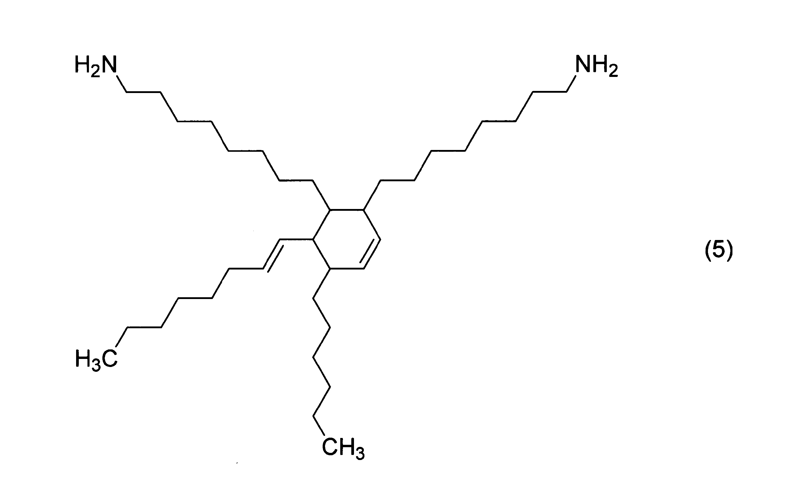
前記構造(a)を有するX1は多価カルボン酸残基であり、構造(a)を有する多価カルボン酸残基またはその誘導体の残基に由来する。多価カルボン酸残基となる多価カルボン酸化合物としては、テトラカルボン酸、ヘキサカルボン酸オクタカルボン酸が挙げられる。また、この多価カルボン酸残基に対応する多価カルボン酸成分を重合時に用いることによって、これらの多価カルボン酸残基を構造単位に含ませることができる。構造(a)を有する多価カルボン酸としては、前述した構造(a)を有するY1で例示した多価アミン類と無水トリメリット酸クロライドとの反応物が挙げられる。より具体的には下記一般式(6)が挙げられる。
X 1 having the structure (a) is a polyvalent carboxylic acid residue, and is derived from a polyvalent carboxylic acid residue having the structure (a) or a residue thereof. Examples of the polyvalent carboxylic acid compound serving as a polyvalent carboxylic acid residue include tetracarboxylic acid and octacarboxylic acid hexacarboxylic acid. Further, by using the polyvalent carboxylic acid component corresponding to the polyvalent carboxylic acid residue at the time of polymerization, these polyvalent carboxylic acid residues can be included in the structural unit. The polyvalent carboxylic acids having the structure (a), include reaction products of polyamines and trimellitic anhydride acid chloride as exemplified by Y 1 having the above structure (a). More specifically, the following general formula (6) can be mentioned.

一般式(6)中、i、j、k、lは自然数であり、i+j=6~17、k+l=8~19である。波線部は炭素-炭素単結合または炭素-炭素二重結合を意味する。
In the general formula (6), i, j, k, l are natural numbers, and i + j = 6 to 17, k + l = 8 to 19. The wavy line part means a carbon-carbon single bond or a carbon-carbon double bond.
前記一般式(11)中、X4は4~6価の有機基を示し、多価カルボン酸成分の残基を示す。多価カルボン酸成分としては、テトラカルボン酸、テトラカルボン酸二無水物またはテトラカルボン酸ジエステルジクロリドなどが挙げられる。Y4は2~6価の有機基を示し、多価アミン残基を示す。X4およびY4のうちの少なくともいずれかは、一以上の脂環構造および複数の炭素数4以上の炭化水素構造を含む有機基(以下、「構造(b)」と省略する場合がある)を示す。すなわち、X4が構造(b)を有する多価カルボン酸残基を示す場合、Y4が(b)を有する多価アミン残基を示す場合、X4とY4がそれぞれ構造(b)を有する多価カルボン酸残基および構造(b)を有する多価アミン残基を示す場合がある。かかる構造を含有することで、樹脂組成物を硬化した硬化膜は、高伸度、低誘電率、低誘電正接を有する。
In the general formula (11), X 4 represents a 4-6 valent organic group, a residue of a polycarboxylic acid component. Examples of the polyvalent carboxylic acid component include tetracarboxylic acid, tetracarboxylic dianhydride, tetracarboxylic acid diester dichloride and the like. Y 4 represents a divalent to hexavalent organic group, a polyamine residue. At least one of X 4 and Y 4, one or more alicyclic structures and a plurality of organic groups comprising C 4+ hydrocarbon structure carbon (hereinafter sometimes abbreviated as "structure (b)") Is shown. That is, when X 4 indicates a polyvalent carboxylic acid residue having a structure (b), and Y 4 indicates a polyvalent amine residue having a structure (b), X 4 and Y 4 have a structure (b), respectively. It may indicate a polyvalent carboxylic acid residue having and a polyvalent amine residue having structure (b). By containing such a structure, the cured film obtained by curing the resin composition has high elongation, low dielectric constant, and low dielectric loss tangent.
前記構造(b)について、具体例を説明する。脂環構造としては、任意の構造を用いることが出来るが、複数の環状構造を有するビシクロ環、トリシクロ環が耐熱性の観点から好ましい。脂環構造の具体例としては、前記構造(a)の脂環式炭化水素の具体例として例示した有機基に加え、ノルボルニル基、ノルボネル基、トリシクロデカニル基などが挙げられ、耐熱性の観点から、ノルボルニル基、ノルボネル基、トリシクロデカニル基が好ましい。
A specific example of the structure (b) will be described. Any structure can be used as the alicyclic structure, but a bicyclo ring and a tricyclo ring having a plurality of cyclic structures are preferable from the viewpoint of heat resistance. Specific examples of the alicyclic structure include an organic group exemplified as a specific example of the alicyclic hydrocarbon of the structure (a), a norbornyl group, a norbonel group, a tricyclodecanyl group and the like, and have heat resistance. From the viewpoint, a norbornyl group, a norbonel group and a tricyclodecanyl group are preferable.
炭素数4以上の炭化水素構造としては、前記構造(a)の不飽和結合を有してもよい炭素数4~12の炭化水素基の具体例として例示した有機基に加え、テトラデカニル基、ヘキサデカニル基、オクタデカニル基、イコサニル基が挙げられる。
As the hydrocarbon structure having 4 or more carbon atoms, in addition to the organic group exemplified as a specific example of the hydrocarbon group having 4 to 12 carbon atoms which may have an unsaturated bond of the structure (a), a tetradecanyl group and a hexadecanyl group are used. Examples include a group, an octadecanol group, and an icosanyl group.
前記構造(b)を有するY4は多価アミン残基であり、多価アミン化合物としては、前記構造(a)で例示した多価アミンに加え、下記一般式(12)で表される多価アミンが挙げられる。
Is Y 4 is a polyvalent amine residue having the structure (b), the polyhydric amine compound, in addition to the polyvalent amine exemplified in the construction (a), the multi represented by the following general formula (12) Valuable amines can be mentioned.

一般式(12)中、uおよびtはそれぞれ4~16の整数を示す。
In the general formula (12), u and t represent integers of 4 to 16, respectively.
前記構造(b)を有するX4は多価カルボン酸残基であり、多価カルボン酸としては、前記構造(a)で例示した多価カルボン酸に加え、下記一般式(13)で表される多価カルボン酸が挙げられる。
X 4 having the structure (b) is a polyvalent carboxylic acid residue, as the polycarboxylic acid, in addition to the polycarboxylic acid exemplified in the construction (a), is represented by the following general formula (13) Polyvalent carboxylic acid.

一般式(13)中、oおよびpはそれぞれ4~16の整数を示す。
In the general formula (13), o and p represent integers of 4 to 16, respectively.
前記(A)成分は、前記一般式(1)および下記一般式(7)で表される構造単位を有する樹脂であることが好ましい。また、前記一般式(11)および下記一般式(7)で表される構造単位を有する樹脂であることが好ましい。これらの構造単位を有することで、低誘電率、低誘電正接を維持しつつ、耐熱性および有機溶媒溶解性を付与することが出来る。
The component (A) is preferably a resin having a structural unit represented by the general formula (1) and the following general formula (7). Further, it is preferable that the resin has a structural unit represented by the general formula (11) and the following general formula (7). By having these structural units, it is possible to impart heat resistance and organic solvent solubility while maintaining a low dielectric constant and a low dielectric loss tangent.

一般式(7)中、X2は4~6価の有機基を示し、Y2は2~6価の有機基を示す。ただし、少なくともX2がX3であるか、Y2がY3である。X3は、ビスフェノールA骨格、ビフェニル骨格若しくはヘキサフルオロイソプロピリデン骨格のいずれか一つ以上を含有する2~6価の有機基、または下記一般式(8)で表される酸無水物の残基のいずれか一つ以上を示す。Y3はビスフェノールA骨格、ビフェニル骨格若しくはヘキサフルオロイソプロピリデン骨格のいずれか一つ以上を含有する2~6価の有機基または下記式(9)で表されるジアミンの残基のいずれか一つ以上を示す。複数のR3は同じでも異なっていてもよく、エチレン性不飽和結合を有する1価の有機基または水素原子を示す。ただし、すべてのR3が水素原子ではない。rは2~4の整数を示す。複数のR4は同じでも異なっていてもよく、カルボキシル基、水酸基またはエチレン性不飽和結合を有する1価の有機基を示す。sは0~4の整数を示す。*は結合点を示す。
In the general formula (7), X 2 represents a 4- to hexavalent organic group, and Y 2 represents a 2- to 6-valent organic group. However, at least X 2 is X 3 or Y 2 is Y 3 . X 3 is a divalent to hexavalent organic group containing any one or more of a bisphenol A skeleton, a biphenyl skeleton or a hexafluoroisopropylidene skeleton, or a residue of an acid anhydride represented by the following general formula (8). Indicates any one or more of. Y 3 is any one of a diamine residue represented by the following formula (9) or a divalent to hexavalent organic group containing any one or more of a bisphenol A skeleton, a biphenyl skeleton or a hexafluoroisopropylidene skeleton. The above is shown. The plurality of R 3 may be the same or different, represents a monovalent organic group or a hydrogen atom with an ethylenically unsaturated bond. However, not all R 3s are hydrogen atoms. r indicates an integer of 2 to 4. The plurality of R 4 may be the same or different, showing a carboxyl group, a monovalent organic group having a hydroxyl group or an ethylenically unsaturated bond. s represents an integer from 0 to 4. * Indicates the connection point.

一般式(8)中、aは6~20の整数を示す。*は結合点を示す。
In the general formula (8), a represents an integer of 6 to 20. * Indicates the connection point.

一般式(9)中、*は結合点を示す。
In general formula (9), * indicates a connection point.
一般式(7)中、X2およびX3はカルボン酸残基またはその誘導体の残基に由来する。X2がX3である場合、X3を酸残基とするカルボン酸化合物としては例えば、3,3’,4,4’-ビフェニルテトラカルボン酸、2,3,3’,4’-ビフェニルテトラカルボン酸、2,2’,3,3’-ビフェニルテトラカルボン酸、2,2-ビス(3,4-ジカルボキシフェニル)ヘキサフルオロプロパン、2,2-ビス(2,3-ジカルボキシフェニル)ヘキサフルオロプロパン、4,4‘-(4,4’-イソプロピリデンジフェノキシ)ビス(フタル酸)、4,4‘-(4,4’-イソプロピリデンジフェノキシカルボニル)ビス(フタル酸)および、前記一般式(7)で挙げられるカルボン酸無水物、およびそれらの誘導体が挙げられる。これらの中でも、有機溶媒への溶解性、透明性、低誘電率性の観点から、2,2-ビス(3,4-ジカルボキシフェニル)ヘキサフルオロプロパン、2,2-ビス(2,3-ジカルボキシフェニル)ヘキサフルオロプロパン、4,4‘-(4,4’-イソプロピリデンジフェノキシ)ビス(フタル酸)が好ましい。
In general formula (7), X 2 and X 3 are derived from carboxylic acid residues or residues of derivatives thereof. When X 2 is X 3 , examples of the carboxylic acid compound having X 3 as an acid residue include 3,3', 4,4'-biphenyltetracarboxylic acid and 2,3,3', 4'-biphenyl. Tetracarboxylic acid, 2,2', 3,3'-biphenyltetracarboxylic acid, 2,2-bis (3,4-dicarboxyphenyl) hexafluoropropane, 2,2-bis (2,3-dicarboxyphenyl) ) Hexafluoropropane, 4,4'-(4,4'-isopropyridene diphenoxy) bis (phthalic acid), 4,4'-(4,4'-isopropyridene diphenoxycarbonyl) bis (phthalic acid) and , Carboxylic acid anhydrides listed in the general formula (7), and derivatives thereof. Among these, 2,2-bis (3,4-dicarboxyphenyl) hexafluoropropane and 2,2-bis (2,3-bis) from the viewpoint of solubility in organic solvents, transparency, and low dielectric constant. Dicarboxyphenyl) hexafluoropropane, 4,4'-(4,4'-isopropyridene diphenoxy) bis (phthalic acid) are preferred.
一般式(7)中、Y2およびY3はアミン残基またはその誘導体の残基に由来する。Y2がY3である場合、Y3をアミン残基とするアミノ化合物としては例えば、4,4’-ジアミノビフェニル、2,2’-ジメチル-4,4’-ジアミノビフェニル、2,2’-ジエチル-4,4’-ジアミノビフェニル、3,3’-ジメチル-4,4’-ジアミノビフェニル、3,3’-ジエチル-4,4’-ジアミノビフェニル、2,2’,3,3’-テトラメチル-4,4’-ジアミノビフェニル、3,3’,4,4’-テトラメチル-4,4’-ジアミノビフェニル、2,2’-ビス(トリフルオロメチル)-4,4’-ジアミノビフェニル、ビス(3-アミノ-4-ヒドロキシ)ビフェニル、4,4’-ジアミノ-6,6’-ビス(トリフルオロメチル)-[1,1’-ビフェニル]-3,3’-ジオール、ビス(4-アミノフェノキシ)ビフェニル、2,2-ビス[4-(4-アミノフェノキシ)フェニル]ヘキサフルオロプロパン、ビス(3-アミノ-4-ヒドロキシフェニル)ヘキサフルオロプロパン、2,2’-ビス[N-(3-アミノベンゾイル)-3-アミノ-4-ヒドロキシフェニル]ヘキサフルオロプロパン、2,2’-ビス[N-(4-アミノベンゾイル)-3-アミノ-4-ヒドロキシフェニル]ヘキサフルオロプロパン、2,2-ビス[4-(4-アミノフェノキシ)フェニル]プロパンまたは、前記一般式(8)で挙げられるジアミン化合物、またはそれらの誘導体が挙げられる。これらの中でも、有機溶媒への溶解性、透明性、低誘電率性の観点から、2,2’-ビス(トリフルオロメチル)-4,4’-ジアミノビフェニル、ビス(3-アミノ-4-ヒドロキシフェニル)ヘキサフルオロプロパン、2,2-ビス[4-(4-アミノフェノキシ)フェニル]プロパンなどの芳香族ジアミンおよび、一般式(9)中の1,4-シクロヘキサンジアミン、1,2-ビス(アミノメチル)シクロヘキサンおよび1,3-ビス(アミノメチル)シクロヘキサンが好ましい。
In general formula (7), Y 2 and Y 3 are derived from amine residues or residues of derivatives thereof. When Y 2 is Y 3 , examples of the amino compound having Y 3 as an amine residue include 4,4'-diaminobiphenyl, 2,2'-dimethyl-4,4'-diaminobiphenyl, 2,2'. -Diethyl-4,4'-diaminobiphenyl, 3,3'-dimethyl-4,4'-diaminobiphenyl, 3,3'-diethyl-4,4'-diaminobiphenyl, 2,2', 3,3'-Tetramethyl-4,4'-diaminobiphenyl,3,3',4,4'-tetramethyl-4,4'-diaminobiphenyl,2,2'-bis (trifluoromethyl) -4,4'- Diaminobiphenyl, bis (3-amino-4-hydroxy) biphenyl, 4,4'-diamino-6,6'-bis (trifluoromethyl)-[1,1'-biphenyl] -3,3'-diol, Bis (4-aminophenoxy) biphenyl, 2,2-bis [4- (4-aminophenoxy) phenyl] hexafluoropropane, bis (3-amino-4-hydroxyphenyl) hexafluoropropane, 2,2'-bis [N- (3-Aminobenzoyl) -3-amino-4-hydroxyphenyl] hexafluoropropane, 2,2'-bis [N- (4-aminobenzoyl) -3-amino-4-hydroxyphenyl] hexafluoro Examples thereof include propane, 2,2-bis [4- (4-aminophenoxy) phenyl] propane, a diamine compound represented by the general formula (8), or a derivative thereof. Among these, 2,2'-bis (trifluoromethyl) -4,4'-diaminobiphenyl, bis (3-amino-4-) from the viewpoint of solubility in organic solvents, transparency, and low dielectric constant. Aromatic diamines such as hydroxyphenyl) hexafluoropropane and 2,2-bis [4- (4-aminophenoxy) phenyl] propane, and 1,4-cyclohexanediamine and 1,2-bis in the general formula (9). (Aminomethyl) cyclohexane and 1,3-bis (aminomethyl) cyclohexane are preferred.
X1は一般式(1)の要件を満たす限り、構造(a)を有する多価カルボン酸残基以外のその他の酸残基でもよい。また、X2は一般式(7)の要件を満たす限り、X3以外のその他の酸残基でもよい。
X 1 may be an acid residue other than the polyvalent carboxylic acid residue having the structure (a) as long as the requirements of the general formula (1) are satisfied. Further, X 2 may be an acid residue other than X 3 as long as it satisfies the requirement of the general formula (7).
また、X4は一般式(11)の要件を満たす限り、構造(b)を有する多価カルボン酸残基以外のその他の酸残基でもよい。
Further, X 4 may be an acid residue other than the polyvalent carboxylic acid residue having the structure (b) as long as the requirements of the general formula (11) are satisfied.
その他の酸残基となるカルボン酸化合物としては例えば、ピロメリット酸、3,3’,4,4’-ベンゾフェノンテトラカルボン酸、2,2’,3,3’-ベンゾフェノンテトラカルボン酸、1,1-ビス(3,4-ジカルボキシフェニル)エタン、1,1-ビス(2,3-ジカルボキシフェニル)エタン、ビス(3,4-ジカルボキシフェニル)メタン、ビス(2,3-ジカルボキシフェニル)メタン、ビス(3,4-ジカルボキシフェニル)スルホン、ビス(3,4-ジカルボキシフェニル)チオエーテル、ビス(3,4-ジカルボキシフェニル)エーテル、1,3-ビス(3,4-ジカルボキシフェノキシ)ベンゼン、トリメリット酸(3,4-ジカルボキシフェニル)、1,2,5,6-ナフタレンテトラカルボン酸、2,3,6,7-ナフタレンテトラカルボン酸、2,3,5,6-ピリジンテトラカルボン酸若しくは3,4,9,10-ペリレンテトラカルボン酸等の芳香族テトラカルボン酸又はビシクロ[3.1.1.]ヘプト-2-エンテトラカルボン酸、ビシクロ[2.2.2.]オクタンテトラカルボン酸若しくはアダマタンテトラカルボン酸等の脂肪族テトラカルボン酸等が挙げられる。
Examples of the carboxylic acid compound as another acid residue include pyromellitic acid, 3,3', 4,4'-benzophenone tetracarboxylic acid, 2,2', 3,3'-benzophenone tetracarboxylic acid, 1, 1-bis (3,4-dicarboxyphenyl) ethane, 1,1-bis (2,3-dicarboxyphenyl) ethane, bis (3,4-dicarboxyphenyl) methane, bis (2,3-dicarboxyphenyl) Phenyl) methane, bis (3,4-dicarboxyphenyl) sulfone, bis (3,4-dicarboxyphenyl) thioether, bis (3,4-dicarboxyphenyl) ether, 1,3-bis (3,4-) Dicarboxyphenoxy) benzene, trimellitic acid (3,4-dicarboxyphenyl), 1,2,5,6-naphthalenetetracarboxylic acid, 2,3,6,7-naphthalenetetracarboxylic acid, 2,3,5 , 6-pyridinetetracarboxylic acid or aromatic tetracarboxylic acid such as 3,4,9,10-perylenetetracarboxylic acid or bicyclo [3.1.1. ] Hept-2-enetetracarboxylic acid, bicyclo [2.2.2. ] Aliphatic tetracarboxylic acids such as octane tetracarboxylic acid and adamatane tetracarboxylic acid can be mentioned.
これらの酸は、そのまま、又は、酸無水物、酸クロリド若しくは活性エステルとして使用できる。活性化エステル基としては以下の構造が挙げられるが、これらに限定されない。
These acids can be used as they are or as acid anhydrides, acid chlorides or active esters. Examples of the activated ester group include, but are not limited to, the following structures.

式中、A及びDは、水素原子、メチル基、エチル基、プロピル基、イソプロピル基、t-ブチル基、トリフルオロメチル基、ハロゲン基、フェノキシ基、ニトロ基を示す。*は結合点を示す。
In the formula, A and D represent a hydrogen atom, a methyl group, an ethyl group, a propyl group, an isopropyl group, a t-butyl group, a trifluoromethyl group, a halogen group, a phenoxy group and a nitro group. * Indicates the connection point.
また、ジメチルシランジフタル酸又は1,3-ビス(フタル酸)テトラメチルジシロキサン等のシリコン原子含有テトラカルボン酸を用いることにより、基板に対する接着性や、洗浄等に用いられる酸素プラズマ、UVオゾン処理に対する耐性を高めることができる。これらシリコン原子含有のテトラカルボン酸は、全酸成分の1~30mol%用いることが好ましい。
Further, by using a silicon atom-containing tetracarboxylic acid such as dimethylsilanediphthalic acid or 1,3-bis (phthalic acid) tetramethyldisiloxane, adhesion to a substrate, oxygen plasma used for cleaning, etc., UV ozone The resistance to treatment can be increased. It is preferable to use 1 to 30 mol% of the total acid component of these silicon atom-containing tetracarboxylic acids.
Y1は一般式(1)の要件を満たす限り、構造(a)を有する多価アミン残基以外のその他のアミン残基でもよい。また、Y2は、一般式(7)の要件を満たす限り、Y3以外のその他のアミン残基でもよい。
Y 1 may be an amine residue other than the polyvalent amine residue having the structure (a) as long as the requirements of the general formula (1) are satisfied. Further, Y 2 may be an amine residue other than Y 3 as long as it satisfies the requirement of the general formula (7).
また、Y4は、一般式(11)の要件を満たす限り、構造(a)を有する多価アミン残基以外のその他のアミン残基でもよい。
Further, Y 4 is as long as it meets the requirements of the general formula (11) may be a polyvalent amine other amine residues other than residue having the structure (a).
その他のアミン残基となる多価アミン化合物としては、例えば、芳香族ジアミンとしては、m-フェニレンジアミン、p-フェニレンジアミン、3,5-ジアミノ安息香酸、1,5-ナフタレンジアミン、2,6-ナフタレンジアミン、9,10-アントラセンジアミン、4,4’-ジアミノベンズアニリド、3,4’-ジアミノジフェニルエーテル、4,4’-ジアミノジフェニルエーテル、3-カルボキシ-4,4’-ジアミノジフェニルエーテル、3-スルホン酸-4,4’-ジアミノジフェニルエーテル、ビス[4-(4-アミノフェノキシ)フェニル]エーテル、1,4-ビス(4-アミノフェノキシ)ベンゼン、1,3-ビス(3-アミノフェノキシ)ベンゼン、1,3-ビス(4-アミノフェノキシ)ベンゼン、ビス(3-アミノ-4-ヒドロキシフェニル)エーテル、3,4’-ジアミノジフェニルメタン、ビス(3-アミノ-4-ヒドロキシフェニル)メチレン、4,4’-ジアミノジフェニルメタン、3,3’-ジアミノジフェニルスルホン、3,4’-ジアミノジフェニルスルホン、4,4’-ジアミノジフェニルスルホン、ビス[N-(3-アミノベンゾイル)-3-アミノ-4-ヒドロキシフェニル]スルホン、ビス[N-(4-アミノベンゾイル)-3-アミノ-4-ヒドロキシフェニル]スルホン、ビス(3-アミノ-4-ヒドロキシフェニル)スルホン、ビス(4-アミノフェノキシフェニル)スルホン、ビス(3-アミノフェノキシフェニル)スルホン、ビス(3-アミノ-4-ヒドロキシフェニル)プロパン、2,2’-ビス[N-(3-アミノベンゾイル)-3-アミノ-4-ヒドロキシフェニル]プロパン、2,2’-ビス[N-(4-アミノベンゾイル)-3-アミノ-4-ヒドロキシフェニル]プロパン、9,9-ビス(3-アミノ-4-ヒドロキシフェニル)フルオレン、2,7-ジアミノフルオレン、9,9-ビス(4-アミノフェニル)フルオレン、9,9-ビス[N-(3-アミノベンゾイル)-3-アミノ-4-ヒドロキシフェニル]フルオレン、9,9-ビス[N-(4-アミノベンゾイル)-3-アミノ-4-ヒドロキシフェニル]フルオレン、2-(4-アミノフェニル)-5-アミノベンゾオキサゾール、2-(3-アミノフェニル)-5-アミノベンゾオキサゾール、2-(4-アミノフェニル)-6-アミノベンゾオキサゾール、2-(3-アミノフェニル)-6-アミノベンゾオキサゾール、1,4-ビス(5-アミノ-2-ベンゾオキサゾリル)ベンゼン、1,4-ビス(6-アミノ-2-ベンゾオキサゾリル)ベンゼン、1,3-ビス(5-アミノ-2-ベンゾオキサゾリル)ベンゼン、1,3-ビス(6-アミノ-2-ベンゾオキサゾリル)ベンゼン、2,6-ビス(4-アミノフェニル)ベンゾビスオキサゾール、2,6-ビス(3-アミノフェニル)ベンゾビスオキサゾール、ビス[(3-アミノフェニル)-5-ベンゾオキサゾリル]、ビス[(4-アミノフェニル)-5-ベンゾオキサゾリル]、ビス[(3-アミノフェニル)-6-ベンゾオキサゾリル]、ビス[(4-アミノフェニル)-6-ベンゾオキサゾリル]、N、N’-ビス(3-アミノベンゾイル)-2,5-ジアミノ-1,4-ジヒドロキシベンゼン、N、N’-ビス(4-アミノベンゾイル)-2,5-ジアミノ-1,4-ジヒドロキシベンゼン、N、N’-ビス(4-アミノベンゾイル)-4,4’-ジアミノ-3,3-ジヒドロキシビフェニル、N、N’-ビス(3-アミノベンゾイル)-3,3’-ジアミノ-4,4-ジヒドロキシビフェニル、N、N’-ビス(4-アミノベンゾイル)-3,3’-ジアミノ-4,4-ジヒドロキシビフェニル、3,4’-ジアミノジフェニルスルフィド、4,4’-ジアミノジフェニルスルフィド、4-アミノ安息香酸4-アミノフェニルエステル、1,3-ビス(4-アニリノ)テトラメチルジシロキサン、などの芳香族ジアミン、およびこれらの芳香族環の水素原子の一部を、炭素数1~10のアルキル基やフルオロアルキル基、ハロゲン原子などで置換した化合物などを挙げることができるが、これらに限定されない。
Examples of polyvalent amine compounds that serve as other amine residues include m-phenylenediamine, p-phenylenediamine, 3,5-diaminobenzoic acid, 1,5-naphthalenediamine, and 2,6 as aromatic diamines. -Naphthalenediamine, 9,10-anthracenediamine, 4,4'-diaminobenzanilide, 3,4'-diaminodiphenyl ether, 4,4'-diaminodiphenyl ether, 3-carboxy-4,4'-diaminodiphenyl ether, 3- Sulphonic acid-4,4'-diaminodiphenyl ether, bis [4- (4-aminophenoxy) phenyl] ether, 1,4-bis (4-aminophenoxy) benzene, 1,3-bis (3-aminophenoxy) benzene , 1,3-bis (4-aminophenoxy) benzene, bis (3-amino-4-hydroxyphenyl) ether, 3,4'-diaminodiphenylmethane, bis (3-amino-4-hydroxyphenyl) methylene, 4, 4'-diaminodiphenylmethane, 3,3'-diaminodiphenylsulfone, 3,4′-diaminodiphenylsulfone, 4,4′-diaminodiphenylsulfone, bis [N- (3-aminobenzoyl) -3-amino-4- Hydroxyphenyl] sulfone, bis [N- (4-aminobenzoyl) -3-amino-4-hydroxyphenyl] sulfone, bis (3-amino-4-hydroxyphenyl) sulfone, bis (4-aminophenoxyphenyl) sulfone, Bis (3-aminophenoxyphenyl) sulfone, bis (3-amino-4-hydroxyphenyl) propane, 2,2'-bis [N- (3-aminobenzoyl) -3-amino-4-hydroxyphenyl] propane, 2,2'-bis [N- (4-aminobenzoyl) -3-amino-4-hydroxyphenyl] propane, 9,9-bis (3-amino-4-hydroxyphenyl) fluorene, 2,7-diaminofluorene , 9,9-bis (4-aminophenyl) fluorene, 9,9-bis [N- (3-aminobenzoyl) -3-amino-4-hydroxyphenyl] fluorene, 9,9-bis [N- (4) -Aminobenzoyl) -3-amino-4-hydroxyphenyl] fluorene, 2- (4-aminophenyl) -5-aminobenzoxazole, 2- (3-aminophenyl) -5-aminobenzoxazole, 2- (4) -Aminophenyl) -6-aminobenzoxazole, 2- (3-amino Phenyl) -6-aminobenzoxazole, 1,4-bis (5-amino-2-benzoxazolyl) benzene, 1,4-bis (6-amino-2-benzoxazolyl) benzene, 1,3 -Bis (5-amino-2-benzoxazolyl) benzene, 1,3-bis (6-amino-2-benzoxazolyl) benzene, 2,6-bis (4-aminophenyl) benzobisoxazole, 2,6-bis (3-aminophenyl) benzobisoxazole, bis [(3-aminophenyl) -5-benzoxazolyl], bis [(4-aminophenyl) -5-benzoxazolyl], bis [(3-Aminophenyl) -6-benzoxazolyl], bis [(4-aminophenyl) -6-benzoxazolyl], N, N'-bis (3-aminobenzoyl) -2,5- Diamino-1,4-dihydroxybenzene, N, N'-bis (4-aminobenzoyl) -2,5-diamino-1,4-dihydroxybenzene, N, N'-bis (4-aminobenzoyl) -4, 4'-diamino-3,3-dihydroxybiphenyl, N, N'-bis (3-aminobenzoyl) -3,3'-diamino-4,4-dihydroxybiphenyl, N, N'-bis (4-aminobenzoyl) ) -3,3'-Diamino-4,4-dihydroxybiphenyl, 3,4'-diaminodiphenylsulfide, 4,4'-diaminodiphenylsulfide, 4-aminobenzoic acid 4-aminophenyl ester, 1,3-bis Aromatic diamines such as (4-anilino) tetramethyldisiloxane, and compounds in which a part of the hydrogen atom of these aromatic rings is replaced with an alkyl group having 1 to 10 carbon atoms, a fluoroalkyl group, a halogen atom, or the like. However, it is not limited to these.
前記の多価アミン化合物は、そのまま、あるいはアミン部位がイソシアネート化またはトリメチルシリル化された化合物として使用できる。また、これら2種以上の多価アミン化合物を組み合わせて用いてもよい。
The above-mentioned multivalent amine compound can be used as it is or as a compound in which the amine moiety is isocyanated or trimethylsilylated. Further, these two or more kinds of polyvalent amine compounds may be used in combination.
脂肪族ジアミンとしては、例えば、エチレンジアミン、1,3-ジアミノプロパン、2-メチル-1,3-プロパンジアミン、1,4-ジアミノブタン、1,5-ジアミノペンタン、2-メチル-1,5-ジアミノペンタン、1,6-ジアミノヘキサン、1,7-ジアミノヘプタン、1,8-ジアミノオクタン、1,9-ジアミノノナン、1,10-ジアミノデカン、1,11-ジアミノウンデカン、1,12-ジアミノドデカン、シロキサン構造を有するジアミンとしては、ビス(3-アミノプロピル)テトラメチルジシロキサン、ビス(p-アミノフェニル)オクタメチルペンタシロキサンが挙げられ、基板との接着性を向上させることができるため、好ましい。
Examples of the aliphatic diamine include ethylenediamine, 1,3-diaminopropane, 2-methyl-1,3-propanediamine, 1,4-diaminobutane, 1,5-diaminopentane, and 2-methyl-1,5-. Diaminopentane, 1,6-diaminohexane, 1,7-diaminoheptane, 1,8-diaminooctane, 1,9-diaminononane, 1,10-diaminodecane, 1,11-diaminoundecane, 1,12-diaminododecane Examples of the diamine having a siloxane structure include bis (3-aminopropyl) tetramethyldisiloxane and bis (p-aminophenyl) octamethylpentasiloxane, which are preferable because they can improve the adhesiveness to the substrate. ..
前記の一般式(1)中の複数のR1、一般式(7)中の複数のR3および一般式(11)中の複数のR8はそれぞれ、少なくとも一つはエチレン性不飽和結合を有する1価の有機基である。エチレン性不飽和結合を有する有機基の導入方法は、例えば、テトラカルボン酸二無水物とエチレン性不飽和結合を有するアルコール類を反応させてテトラカルボン酸ジエステルを生成後、これと多価アミン化合物とのアミド重縮合反応によって得られる。その他の方法としては例えば、酸二無水物とジアミンよりポリアミド酸を得たのち、トリフルオロ酢酸およびエチレン性不飽和結合を有するアルコール類を、該アミド酸と反応させる方法などが挙げられる。
A plurality of R 1 in the general formula (1) in the general formula (7) each of the plurality of the plurality of R 8 R 3 and Formula (11) in the in, at least one ethylenically unsaturated bond It is a monovalent organic group having. As a method for introducing an organic group having an ethylenically unsaturated bond, for example, a tetracarboxylic acid dianhydride is reacted with an alcohol having an ethylenically unsaturated bond to form a tetracarboxylic acid diester, which is then combined with a polyvalent amine compound. It is obtained by an amide polycondensation reaction with. Other methods include, for example, a method in which a polyamic acid is obtained from an acid dianhydride and a diamine, and then an alcohol having a trifluoroacetic acid and an ethylenically unsaturated bond is reacted with the amic acid.
前述のテトラカルボン酸ジエステルの生成方法としては、そのまま前述の酸二無水物およびアルコールを溶媒中にて反応させることもできるが、反応性の観点から反応活性化剤を用いることが好ましい。反応活性化剤としてはピリジン、ジメチルアミノピリジン、トリエチルアミン、N-メチルモルホリン、1,8-ジアザビシクロウンデセンなどの3級アミンがあげられる。反応活性化剤の添加量としては、反応させる酸無水物基に対して3mol%以上300mol%以下が好ましく、より好ましくは20mol%以上150mol%以下である。また、反応中にエチレン性不飽和結合部位が架橋することを防ぐ目的で、重合禁止剤を少量用いてもよい。これにより反応性が低いエチレン性不飽和結合を有するアルコール類とテトラカルボン酸二無水物との反応において、120℃以下の範囲で加熱し、反応を促進することができる。重合禁止剤としては、ハイドロキノン、4-メトキシフェノール、t-ブチルピロカテコール、ビス-t-ブチルヒドロキシトルエンなどのフェノール化合物が挙げられる。重合禁止剤の添加量としては、アルコール類のエチレン性不飽和結合に対して、重合禁止剤のフェノール性水酸基が0.1mol%以上5mol%以下が好ましい。
As the method for producing the above-mentioned tetracarboxylic dianhydride, the above-mentioned acid dianhydride and alcohol can be reacted as they are in a solvent, but it is preferable to use a reaction activator from the viewpoint of reactivity. Examples of the reaction activator include tertiary amines such as pyridine, dimethylaminopyridine, triethylamine, N-methylmorpholine, and 1,8-diazabicycloundecene. The amount of the reaction activator added is preferably 3 mol% or more and 300 mol% or less, more preferably 20 mol% or more and 150 mol% or less, based on the acid anhydride group to be reacted. In addition, a small amount of a polymerization inhibitor may be used for the purpose of preventing the ethylenically unsaturated bond site from being crosslinked during the reaction. As a result, in the reaction between alcohols having an ethylenically unsaturated bond having low reactivity and tetracarboxylic dianhydride, the reaction can be promoted by heating in a range of 120 ° C. or lower. Examples of the polymerization inhibitor include phenol compounds such as hydroquinone, 4-methoxyphenol, t-butylpyrocatechol, and bis-t-butylhydroxytoluene. The amount of the polymerization inhibitor added is preferably 0.1 mol% or more and 5 mol% or less of the phenolic hydroxyl group of the polymerization inhibitor with respect to the ethylenically unsaturated bond of alcohols.
前述のアミド重縮合反応としては種々の方法があげられる。テトラカルボン酸ジエステルを酸クロライド化した後にジアミンと反応させる方法、カルボジイミド系脱水縮合剤を用いる方法、および活性化エステル化した後にジアミンと反応させる方法が挙げられる。中でも、活性化エステルを中間体とする方法は芳香族ジアミンおよび脂肪族ジアミンいずれをモノマーとして選択しても反応性が良好なため、好ましい。
Various methods can be mentioned as the above-mentioned amide polycondensation reaction. Examples thereof include a method of acid chloride-forming a tetracarboxylic acid diester and then reacting it with a diamine, a method using a carbodiimide-based dehydration condensing agent, and a method of activating esterification and then reacting it with a diamine. Of these, the method using an activated ester as an intermediate is preferable because the reactivity is good regardless of whether aromatic diamine or aliphatic diamine is selected as the monomer.
前述のエチレン性不飽和結合を有するアルコール類としては、水酸基を有する(メタ)アクリレートまたは不飽和脂肪酸変性アルコールが挙げられる。水酸基を有する(メタ)アクリレートとしては、2-ヒドロキシエチル(メタ)アクリレート、2-ヒドロキシプロピル(メタ)アクリレート、2-ヒドロキシブチル(メタ)アクリレート、1-(メタ)アクリロイルオキシ-2-プロピルアルコール、2-(メタ)アクリルアミドエチルアルコール、メチロールビニルケトン、2-ヒドロキシエチルビニルケトン、2-ヒドロキシ-3-メトキシプロピル(メタ)アクリレート、2-ヒドロキシ-3-ブトキシプロピル(メタ)アクリレート、2-ヒドロキシ-3-フェノキシプロピル(メタ)アクリレート、2-ヒドロキシ-3-t-ブトキシプロピル(メタ)アクリレート、2-ヒドロキシ-3-シクロヘキシルアルコキシプロピル(メタ)アクリレート、2-ヒドロキシ-3-シクロヘキシロキシプロピル(メタ)アクリレート、2-(メタ)アクリロキシエチル-2-ヒドロキシプロピルフタレートなどの、エチレン性不飽和結合と水酸基を1ずつ有するアルコール、グリセリン-1、3-ジ(メタ)アクリレート、グリセリン-1、2-ジ(メタ)アクリレート、トリメチロールプロパンジ(メタ)アクリレート、ペンタエリスリトールトリ(メタ)アクリレート、ジペンタエリスリトールペンタ(メタ)アクリレート、グリセリン-1-アリロキシ-3-メタクリレート、グリセリン-1-アリロキシ-2-メタクリレート、2―エチル-2-(ヒドロキシメチル)プロパン-1、3-ジイルビス(2-メタクリレート)、2-(アクリロイロキシ)-2-(ヒドロキシメチル)ブチルメタクリレートなどの、エチレン性不飽和結合を2以上と水酸基を1有するアルコールなどが挙げられる。ここで、「(メタ)アクリレート」とは、メタクリレートまたはアクリレートを示す。類似の表記についても同様である。
Examples of the alcohols having an ethylenically unsaturated bond include (meth) acrylates having a hydroxyl group and unsaturated fatty acid-modified alcohols. Examples of the (meth) acrylate having a hydroxyl group include 2-hydroxyethyl (meth) acrylate, 2-hydroxypropyl (meth) acrylate, 2-hydroxybutyl (meth) acrylate, 1- (meth) acryloyloxy-2-propyl alcohol, and the like. 2- (Meta) acrylamide ethyl alcohol, methylol vinyl ketone, 2-hydroxyethyl vinyl ketone, 2-hydroxy-3-methoxypropyl (meth) acrylate, 2-hydroxy-3-butoxypropyl (meth) acrylate, 2-hydroxy- 3-Phenoxypropyl (meth) acrylate, 2-hydroxy-3-t-butoxypropyl (meth) acrylate, 2-hydroxy-3-cyclohexylalkoxypropyl (meth) acrylate, 2-hydroxy-3-cyclohexyloxypropyl (meth) Alcohols such as acrylate, 2- (meth) acryloxyethyl-2-hydroxypropylphthalate, which have an ethylenically unsaturated bond and one hydroxyl group, glycerin-1,3-di (meth) acrylate, glycerin-1,2- Di (meth) acrylate, trimethylpropandi (meth) acrylate, pentaerythritol tri (meth) acrylate, dipentaerythritol penta (meth) acrylate, glycerin-1-allyloxy-3-methacrylate, glycerin-1-allyloxy-2- Two or more ethylenically unsaturated bonds such as methacrylate, 2-ethyl-2- (hydroxymethyl) propane-1,3-diylbis (2-methacrylate), 2- (acryloyloxy) -2- (hydroxymethyl) butyl methacrylate, etc. And alcohol having 1 hydroxyl group. Here, "(meth) acrylate" means methacrylate or acrylate. The same applies to similar notations.
不飽和脂肪酸変性アルコールとしては、炭素数6以上の不飽和脂肪酸変性アルコールが挙げられる。露光感度の観点から、末端に不飽和基を有するか、シス構造の二重結合を有するアルコールが好ましく、誘電率、誘電正接の観点からは、炭素数12以上が好ましい。不飽和脂肪酸変性アルコールの具体例としては、5-ヘキセンー1-オール、3-ヘキセンー1-オール、6-ヘプテン-1-オール、cis-5-オクテン-1-オール、cis-3-オクテン-1-オール、cis-3-ノネン-1-オール、cis-6-ノネン-1-オール、9-デカン-1-オール、cis-4-デカン-1-オール、10-ウンデセン-1-オール、11-ドデカン-1-オール、エライドリノレイルアルコール、オレイルアルコール、リノレイルアルコール、リノレニルアルコール およびエルシルアルコールなどが挙げられる。これらの中から、得られる硬化膜の誘電特性と露光感度の観点から、オレイルアルコール、リノレイルアルコール、リノレニルアルコールが好ましい。
Examples of unsaturated fatty acid-modified alcohols include unsaturated fatty acid-modified alcohols having 6 or more carbon atoms. From the viewpoint of exposure sensitivity, an alcohol having an unsaturated group at the terminal or having a double bond having a cis structure is preferable, and from the viewpoint of dielectric constant and dielectric loss tangent, 12 or more carbon atoms are preferable. Specific examples of unsaturated fatty acid-modified alcohols include 5-hexen-1-ol, 3-hexen-1-ol, 6-heptene-1-ol, cis-5-octene-1-ol, and cis-3-octen-1. -All, cis-3-nonen-1-ol, cis-6-nonen-1-ol, 9-decane-1-ol, cis-4-decane-1-ol, 10-undecene-1-ol, 11 -Dodecane-1-ol, eride linoleil alcohol, oleyl alcohol, linoleil alcohol, linolenyl alcohol, elsyl alcohol and the like. Of these, oleyl alcohol, linoleyl alcohol, and linoleyl alcohol are preferable from the viewpoint of the dielectric properties of the obtained cured film and the exposure sensitivity.
酸無水物とエチレン性不飽和結合を有すアルコール類を反応させる際に、その他のアルコールを同時に用いてもよい。その他のアルコールは、露光感度の調整、有機溶媒への溶解性の調整など様々な目的に合わせて適宜選択できる。具体的にはメタノール、エタノール、1-プロパノール、2-プロパノール、1-ブタノール、2-ブタノール、i-ブタノール、t-ブタノール、1-ペンタノール、2-ペンタノール、3-ペンタノール、i-ペンタノールなどの脂肪族アルコールまたは、エチレングリコールモノメチルエーテル、エチレングリコールモノエチルエーテル、エチレングリコールモノブチルエーテル、ジエチレングリコールモノメチルエーテル、ジエチレングリコールモノエチルエーテル、ジエチレングリコールモノブチルエーテル、トリエチレングリコールモノメチルエーテル、トリエチレングリコールモノエチルエーテル、トリエチレングリコールモノブチルエーテル、プロピレングリコールモノメチルエーテル、プロピレングリコールモノエチルエーテル、プロピレングリコールモノブチルエーテル、ジプロピレングリコールモノメチルエーテル、ジプロピレングリコールモノエチルエーテル、ジプロピレングリコールモノブチルエーテル、トリプロピレングリコールモノメチルエーテル、トリプロピレングリコールモノエチルエーテル、トリプロピレングリコールモノブチルエーテルなどのアルキレンオキサイド由来のモノアルコールなどが挙げられる。
Other alcohols may be used at the same time when the acid anhydride and alcohols having an ethylenically unsaturated bond are reacted. Other alcohols can be appropriately selected according to various purposes such as adjustment of exposure sensitivity and adjustment of solubility in an organic solvent. Specifically, methanol, ethanol, 1-propanol, 2-propanol, 1-butanol, 2-butanol, i-butanol, t-butanol, 1-pentanol, 2-pentanol, 3-pentanol, i-pen Aliper alcohols such as tanol or ethylene glycol monomethyl ether, ethylene glycol monoethyl ether, ethylene glycol monobutyl ether, diethylene glycol monomethyl ether, diethylene glycol monoethyl ether, diethylene glycol monobutyl ether, triethylene glycol monomethyl ether, triethylene glycol monoethyl ether, Triethylene glycol monobutyl ether, propylene glycol monomethyl ether, propylene glycol monoethyl ether, propylene glycol monobutyl ether, dipropylene glycol monomethyl ether, dipropylene glycol monoethyl ether, dipropylene glycol monobutyl ether, tripropylene glycol monomethyl ether, tripropylene glycol Examples thereof include monoalcohol derived from alkylene oxide such as monoethyl ether and tripropylene glycol monobutyl ether.
一般式(1)中のR1、一般式(7)中のR3、および一般式(11)中の複数のR8にエチレン性不飽和結合を有する有機基を導入する方法として、イオン結合を介してもよい。イオン結合によるエチレン性不飽和結合を有する有機基の導入方法としては例えば、酸二無水物とジアミンとの反応により得られたポリアミド酸と、エチレン性不飽和結合を有する三級アミンを反応させる方法が挙げられる。エチレン性不飽和結合を有する三級アミンとしては、下記一般式(10)で表される化合物が挙げられる。
As a method for introducing an organic group R 1 in the general formula (1), the general formula (7) in R 3, and in formula (11) a plurality of R 8 in having an ethylenically unsaturated bond, an ionic bond May be via. As a method for introducing an organic group having an ethylenically unsaturated bond by an ionic bond, for example, a method of reacting a polyamic acid obtained by a reaction between an acid dianhydride and a diamine with a tertiary amine having an ethylenically unsaturated bond. Can be mentioned. Examples of the tertiary amine having an ethylenically unsaturated bond include a compound represented by the following general formula (10).

一般式(10)中、R5は水素原子またはメチル基を示す。R6およびR7はそれぞれ独立に、メチル基、エチル基、n-プロピル基、i-プロピル基、n-ブチル基、s-ブチル基、t-ブチル基またはフェニル基のいずれかを示す。bは1~10の整数を示す。
In the general formula (10), R 5 represents a hydrogen atom or a methyl group. R 6 and R 7 each independently represent either a methyl group, an ethyl group, an n-propyl group, an i-propyl group, an n-butyl group, an s-butyl group, a t-butyl group or a phenyl group. b represents an integer from 1 to 10.
これらの中から、ジメチルアミノエチル(メタ)アクリレート、ジエチルアミノエチル(メタ)アクリレート、ジメチルアミノプロピル(メタ)アクリレート、ジエチルアミノプロピル(メリレートが、露光感度を高めやすく、好ましい。
Among these, dimethylaminoethyl (meth) acrylate, diethylaminoethyl (meth) acrylate, dimethylaminopropyl (meth) acrylate, and diethylaminopropyl (merylate are preferable because they can easily increase the exposure sensitivity.
また、本発明の感光性樹脂組成物の保存安定性向上や様々な機能を発現させるため、(A)成分は主鎖末端を末端封止剤で封止してもよい。末端封止剤としては、モノアミン、酸無水物、モノカルボン酸、モノ酸クロリド化合物、モノ活性エステル化合物などが挙げられる。また、前述のアミド重縮合の反応後期において、モノアルコールを末端封止剤として用いることもできる。また、樹脂の末端を水酸基、カルボキシル基、スルホン酸基、チオール基、ビニル基、エチニル基またはアリル基を有する末端封止剤により封止することで、露光感度、得られる硬化膜の機械特性などを好ましい範囲に容易に調整することができる。
Further, in order to improve the storage stability of the photosensitive resin composition of the present invention and to exhibit various functions, the component (A) may be sealed at the end of the main chain with an end-capping agent. Examples of the terminal encapsulant include monoamines, acid anhydrides, monocarboxylic acids, monoacid chloride compounds, and monoactive ester compounds. In addition, monoalcohol can also be used as an end-capping agent in the latter stage of the above-mentioned amide polycondensation reaction. Further, by sealing the end of the resin with a terminal sealant having a hydroxyl group, a carboxyl group, a sulfonic acid group, a thiol group, a vinyl group, an ethynyl group or an allyl group, exposure sensitivity, mechanical properties of the obtained cured film, etc. Can be easily adjusted to a preferable range.
末端封止剤の導入割合は、現像液への溶解性および得られる硬化膜の機械特性の観点から、0.1mol%以上60mol%以下が好ましく、特に好ましくは5mol%以上50mol%以下である。複数の末端封止剤を反応させ、複数の異なる末端基を導入してもよい。
The introduction ratio of the end sealant is preferably 0.1 mol% or more and 60 mol% or less, and particularly preferably 5 mol% or more and 50 mol% or less, from the viewpoint of solubility in a developing solution and mechanical properties of the obtained cured film. A plurality of end sealants may be reacted to introduce a plurality of different end groups.
末端封止剤に用いるモノアミンとしては公知の化合物を用いることが出来るが、アニリン、2-エチニルアニリン、3-エチニルアニリン、4-エチニルアニリン、1-ヒドロキシ-7-アミノナフタレン、1-カルボキシ-7-アミノナフタレン、3-アミノ安息香酸、3-アミノフェノール、3-アミノチオフェノール、などが好ましい。これらを2種以上用いてもよい。
Known compounds can be used as the monoamine used for the terminal sealant, but aniline, 2-ethynylaniline, 3-ethynylaniline, 4-ethynylaniline, 1-hydroxy-7-aminonaphthalene, 1-carboxy-7 -Aminonaphthalene, 3-aminobenzoic acid, 3-aminophenol, 3-aminothiophenol, etc. are preferable. Two or more of these may be used.
酸無水物、モノカルボン酸、モノ酸クロリド化合物、モノ活性エステル化合物としては、公知の化合物を用いることが出来るが、無水フタル酸、無水マレイン酸、ナジック酸無水物、シクロヘキサンジカルボン酸無水物、3-ヒドロキシフタル酸無水物などの酸無水物、イタコン酸無水物などが好ましい。これらを2種以上用いてもよい。
Known compounds can be used as the acid anhydride, monocarboxylic acid, monoacid chloride compound, and monoactive ester compound, but phthalic anhydride, maleic anhydride, nadic acid anhydride, cyclohexanedicarboxylic acid anhydride, 3 -Acid anhydrides such as hydroxyphthalic anhydride and itaconic anhydride are preferable. Two or more of these may be used.
末端封止剤に用いるモノアルコールとしては、前述の酸無水物と反応するアルコール類として例示したものが挙げられる。
Examples of the monoalcohol used as the terminal sealant include those exemplified as alcohols that react with the acid anhydride described above.
また、本発明に用いる(A)成分に導入された構造(a)を含むモノマ―や末端封止剤は、以下の方法で容易に検出できる。例えば、末端封止剤が導入された樹脂を、酸性溶液に溶解し、構造単位であるアミン成分と酸無水物成分に分解し、これをガスクロマトグラフィー(GC)や、NMR測定することにより、本発明に使用の末端封止剤を容易に検出できる。また、GC測定を各成分とピークの重ならない外部標準物質と同時に測定を行い、クロマトグラムの各ピークの積分値を外部標準物質と比較することで、末端封止剤を含めた各モノマーのモル比を見積もることができる。これとは別に、末端封止剤が導入された樹脂成分を直接、熱分解ガスクロマトグラフ(PGC)や赤外スペクトル、1H-NMRスペクトル、13C-NMRスペクトルおよび2次元NMRスペクトルで測定することによっても、容易に検出可能である。この場合、赤外スペクトル、1H-NMRスペクトルまたは2次元NMRの積分値より各モノマーのモル比を分析可能である。
Further, the monomer and the end-capping agent containing the structure (a) introduced into the component (A) used in the present invention can be easily detected by the following method. For example, a resin into which an end-capping agent has been introduced is dissolved in an acidic solution, decomposed into an amine component and an acid anhydride component, which are structural units, and this is measured by gas chromatography (GC) or NMR. The end-capping agent used in the present invention can be easily detected. In addition, the GC measurement is performed at the same time as the external standard substance whose peaks do not overlap with each component, and the integral value of each peak of the chromatogram is compared with the external standard substance. The ratio can be estimated. Separately, the resin component into which the terminal encapsulant has been introduced shall be directly measured by a pyrolysis gas chromatograph (PGC), an infrared spectrum, a 1 H-NMR spectrum, a 13 C-NMR spectrum and a two-dimensional NMR spectrum. It can also be easily detected by. In this case, the molar ratio of each monomer can be analyzed from the integrated value of the infrared spectrum, 1 H-NMR spectrum or two-dimensional NMR.
本発明における(A)成分は、重量平均分子量5,000以上100,000以下であることが好ましい。重量平均分子量は、GPC(ゲルパーミエーションクロマトグラフィー)によるポリスチレン換算で5,000以上とすることにより、硬化後の伸度、破断点強度、弾性率といった機械特性を向上させることができる。一方、重量平均分子量を100,000以下とすることにより、現像性を向上させることができる。機械特性を得るため、20,000以上がより好ましい。また、(A)成分が2種以上の樹脂を含有する場合、少なくとも1種の重量平均分子量が上記範囲であればよい。
The component (A) in the present invention preferably has a weight average molecular weight of 5,000 or more and 100,000 or less. By setting the weight average molecular weight to 5,000 or more in terms of polystyrene by GPC (gel permeation chromatography), mechanical properties such as elongation after curing, strength at break point, and elastic modulus can be improved. On the other hand, by setting the weight average molecular weight to 100,000 or less, the developability can be improved. More than 20,000 is more preferable in order to obtain mechanical properties. When the component (A) contains two or more kinds of resins, the weight average molecular weight of at least one kind may be in the above range.
また、本発明に用いる(A)成分は溶媒を用いて重合することが好ましい。重合溶媒は、原料モノマーである酸成分、アミン成分、アルコール類、触媒が溶解できればよく、その種類は特に限定されない。例えば、N,N-ジメチルホルムアミド、N,N-ジメチルアセトアミド、N-メチル-2-ピロリドン、1,3-ジメチル-2-イミダゾリジノン、N,N’-ジメチルプロピレン尿素、N,N-ジメチルイソ酪酸アミド、メトキシ-N,N-ジメチルプロピオンアミドのアミド類、γ-ブチロラクトン、γ-バレロラクトン、δ-バレロラクトン、γ-カプロラクトン、ε-カプロラクトン、α-メチル-γ-ブチロラクトンなどの環状エステル類、エチレンカーボネート、プロピレンカーボネートなどのカーボネート類、トリエチレングリコールなどのグリコール類、m-クレゾール、p-クレゾールなどのフェノール類、アセトフェノン、1,3-ジメチル-2-イミダゾリジノン、スルホラン、ジメチルスルホキシドなどを挙げることができる。
Further, the component (A) used in the present invention is preferably polymerized using a solvent. The type of the polymerization solvent is not particularly limited as long as it can dissolve the acid component, the amine component, the alcohols, and the catalyst which are the raw material monomers. For example, N, N-dimethylformamide, N, N-dimethylacetamide, N-methyl-2-pyrrolidone, 1,3-dimethyl-2-imidazolidinone, N, N'-dimethylpropylene urea, N, N-dimethyliso. Cyclic esters such as butyric acid amide, methoxy-N, N-dimethylpropionamide amides, γ-butyrolactone, γ-valerolactone, δ-valerolactone, γ-caprolactone, ε-caprolactone, α-methyl-γ-butyrolactone , Ester carbonates, carbonates such as propylene carbonate, glycols such as triethylene glycol, phenols such as m-cresol and p-cresol, acetophenone, 1,3-dimethyl-2-imidazolidinone, sulfolane, dimethylsulfoxide, etc. Can be mentioned.
本発明の感光性樹脂組成物は、(B)光重合開始剤を含有する。(B)光重合開始剤を含有することで、露光および現像工程を経て、パターン加工が可能となる。(B)光重合開始剤は、露光によりラジカルを発生する化合物であれば特に制限はないが、アルキルフェノン化合物、アミノベンゾフェノン化合物、ジケトン化合物、ケトエステル化合物、ホスフィンオキサイド化合物、オキシムエステル化合物および安息香酸エステル化合物が感度、安定性、合成容易性に優れため好ましい。中でも、感度の観点からアルキルフェノン化合物、オキシムエステル化合物が好ましく、オキシムエステル化合物が特に好ましい。また、加工膜厚が5μm以上の厚膜の場合、解像度の観点からホスフィンオキサイド化合物が好ましい。
The photosensitive resin composition of the present invention contains (B) a photopolymerization initiator. (B) By containing the photopolymerization initiator, pattern processing becomes possible through the exposure and development steps. The photopolymerization initiator (B) is not particularly limited as long as it is a compound that generates radicals upon exposure, but is an alkylphenone compound, an aminobenzophenone compound, a diketone compound, a ketoester compound, a phosphine oxide compound, an oxime ester compound and a benzoic acid ester. The compound is preferable because it has excellent sensitivity, stability, and ease of synthesis. Among them, an alkylphenone compound and an oxime ester compound are preferable from the viewpoint of sensitivity, and an oxime ester compound is particularly preferable. Further, in the case of a thick film having a processed film thickness of 5 μm or more, a phosphine oxide compound is preferable from the viewpoint of resolution.
アルキルフェノン化合物としては、例えば、2-メチル-[4-(メチルチオ)フェニル]-2-モルフォリノプロパン-1-オン、2-ジメチルアミノ-2-(4-メチルベンジル)-1-(4-モルフォリン-4-イル-フェニル)-ブタン-1-オン又は2-ベンジル-2-ジメチルアミノ-1-(4-モルフォリノフェニル)-ブタノン-1などのα-アミノアルキルフェノン化合物、2-ヒドロキシ-2-メチル-1-フェニルプロパン-1-オン、1-(4-イソプロピルフェニル)-2-ヒドロキシ-2-メチルプロパン-1-オン、4-(2-ヒドロキシエトキシ)フェニル-(2-ヒドロキシ-2-プロピル)ケトン、2-ヒロドキシ-1-{4-[4-(2-ヒドロキシ-2-メチル-プロピオニル)-ベンジル]フェニル}-2-メチル-プロパン-1-オン、1-ヒドロキシシクロヘキシル-フェニルケトン、ベンゾインなどのα-ヒドロキシアルキルフェノン化合物、4-ベンゾイル-4-メチルフェニルケトン、2,3-ジエトキシアセトフェノン、2,2-ジメトキシ-2-フェニル-2-フェニルアセトフェノン、2-ヒドロキシ-2-メチルプロピオフェノン、p-t-ブチルジクロロアセトフェノン、ベンジルメトキシエチルアセタール、2,3-ジエトキシアセトフェノン、ベンジルジメチルケタール、ベンゾインエチルエーテル、ベンゾインイソプロピルエーテル、ベンゾインイソブチルエーテル、などのα-アルコキシアルキルフェノン化合物、アセトフェノン、p-t-ブチルジクロロアセトフェノンなどのアセトフェノン化合物が挙げられる。これらの中でも、2-メチル-[4-(メチルチオ)フェニル]-2-モルフォリノプロパン-1-オン、2-ジメチルアミノ-2-(4-メチルベンジル)-1-(4-モルフォリン-4-イル-フェニル)-ブタン-1-オン又は2-ベンジル-2-ジメチルアミノ-1-(4-モルフォリノフェニル)-ブタノン-1などのα-アミノアルキルフェノン化合物が、感度が高いため好ましい。
Examples of the alkylphenone compound include 2-methyl- [4- (methylthio) phenyl] -2-morpholinopropane-1-one and 2-dimethylamino-2- (4-methylbenzyl) -1- (4-). Α-Aminoalkylphenone compounds such as morpholin-4-yl-phenyl) -butane-1-one or 2-benzyl-2-dimethylamino-1- (4-morpholinophenyl) -butanone-1, 2-hydroxy -2-Methyl-1-phenylpropane-1-one, 1- (4-isopropylphenyl) -2-hydroxy-2-methylpropane-1-one, 4- (2-hydroxyethoxy) phenyl- (2-hydroxy) -2-propyl) ketone, 2-hirodoxy-1- {4- [4- (2-hydroxy-2-methyl-propionyl) -benzyl] phenyl} -2-methyl-propane-1-one, 1-hydroxycyclohexyl -Α-Hydroxyalkylphenone compounds such as phenylketone and benzoin, 4-benzoyl-4-methylphenylacetophenone, 2,3-diethoxyacetophenone, 2,2-dimethoxy-2-phenyl-2-phenylacetophenone, 2-hydroxy Α-alkoxy such as -2-methylpropiophenone, pt-butyldichloroacetophenone, benzylmethoxyethylacetophenone, 2,3-diethoxyacetophenone, benzyldimethylketal, benzoinethyl ether, benzoinisopropyl ether, benzoinisobutyl ether, etc. Examples thereof include acetophenone compounds such as alkylphenone compounds, acetophenone, and pt-butyldichloroacetophenone. Among these, 2-methyl- [4- (methylthio) phenyl] -2-morpholinopropane-1-one, 2-dimethylamino-2- (4-methylbenzyl) -1- (4-morpholin-4) Α-Aminoalkylphenone compounds such as -yl-phenyl) -butane-1-one or 2-benzyl-2-dimethylamino-1- (4-morpholinophenyl) -butanone-1 are preferred because of their high sensitivity.
ホスフィンオキサイド化合物としては、例えば、6-トリメチルベンゾイルフェニルホスフィンオキサイド、ビス(2,4,6-トリメチルベンゾイル)-フェニルホスフィンオキサイド、ビス(2,6-ジメトキシベンゾイル)-(2,4,4-トリメチルペンチル)-ホスフィンオキサイドが挙げられる。
Examples of the phosphine oxide compound include 6-trimethylbenzoylphenylphosphine oxide, bis (2,4,6-trimethylbenzoyl) -phenylphosphine oxide, and bis (2,6-dimethoxybenzoyl)-(2,4,4-trimethyl). Penthyl) -phosphine oxide.
オキシムエステル化合物としは、例えば、1-フェニル-1,2-プロパンジオン-2-(o-エトキシカルボニル)オキシム、1-フェニル-1,2-プロパンジオン-2-(o-メトキシカルボニル)オキシム、1-フェニル-2-(ベンゾイルオキシムイミノ)-1-プロパノン、2-オクタンジオン,1-[4-(フェニルチオ)-2-(O-ベンゾイルオキシム)]、1-フェニル-1,2-ブタジオン-2-(o-メトキシカルボニル)オキシム、1,3-ジフェニルプロパントリオン-2-(o-エトキシカルボニル)オキシム、エタノン,1-フェニル-1,2-プロパンジオン-2-(o-ベンゾイル)オキシム、1-フェニル-3-エトキシプロパントリオン-2-(o-ベンゾイル)オキシム、1-[9-エチル-6-(2-メチルベンゾイル)-9H-カルバゾール-3-イル]-,1-(0-アセチルオキシム)、1-[9-エチル-6-(2-メチルベンゾイル)-9H-カルバゾール-3-イル]-,1-(0-アセチルオキシム)、NCI-831、NCI-930(以上、ADEKA製)、OXE-03,OXE-04(以上、BASF製)などが挙げられる。これらの中でも、感度の観点から、1-[9-エチル-6-(2-メチルベンゾイル)-9H-カルバゾール-3-イル]-,1-(0-アセチルオキシム)、2-オクタンジオン,1-[4-(フェニルチオ)-2-(O-ベンゾイルオキシム)]、NCI-831、NCI-930、OXE-03,OXE-04が好ましい。
Examples of the oxime ester compound include 1-phenyl-1,2-propanedione-2- (o-ethoxycarbonyl) oxime, 1-phenyl-1,2-propanedione-2- (o-methoxycarbonyl) oxime, and the like. 1-Phenyl-2- (benzoyloxime imino) -1-propanone, 2-octanedione, 1- [4- (phenylthio) -2- (O-benzoyloxime)], 1-phenyl-1,2-butadione- 2- (o-methoxycarbonyl) oxime, 1,3-diphenylpropanthrion-2- (o-ethoxycarbonyl) oxime, etanone, 1-phenyl-1,2-propanedione-2- (o-benzoyl) oxime, 1-Phenyl-3-ethoxypropanetrione-2- (o-benzoyl) oxime, 1- [9-ethyl-6- (2-methylbenzoyl) -9H-carbazole-3-yl]-, 1- (0-) Acetyloxime), 1- [9-ethyl-6- (2-methylbenzoyl) -9H-carbazole-3-yl]-, 1- (0-acetyloxime), NCI-831, NCI-930 (above, ADEKA) XXE-03, OXE-04 (above, manufactured by BASF) and the like. Among these, from the viewpoint of sensitivity, 1- [9-ethyl-6- (2-methylbenzoyl) -9H-carbazole-3-yl]-, 1- (0-acetyloxime), 2-octanedione, 1 -[4- (Phenylthio) -2- (O-benzoyloxime)], NCI-831, NCI-930, OXE-03, OXE-04 are preferable.
アミノベンゾフェノン化合物としては、例えば、4,4-ビス(ジメチルアミノ)ベンゾフェノン、4,4-ビス(ジエチルアミノ)ベンゾフェノンが挙げられる。
ジケトン化合物としては、ベンジルが挙げられる。
ケトエステル化合物としては、ベンゾイルギ酸メチル、ベンゾイルギ酸エチルが挙げられる。 Examples of the aminobenzophenone compound include 4,4-bis (dimethylamino) benzophenone and 4,4-bis (diethylamino) benzophenone.
Examples of the diketone compound include benzyl.
Examples of the ketoester compound include methyl benzoyl formate and ethyl benzoyl formate.
安息香酸エステル化合物としては、o-ベンゾイル安息香酸メチル、p-ジメチルアミノ安息香酸エチル、4-(ジメチルアミノ)安息香酸2-エチルヘキシル、p-ジエチルアミノ安息香酸エチルが挙げられる。
Examples of the benzoic acid ester compound include methyl o-benzoyl benzoate, ethyl p-dimethylaminobenzoate, 2-ethylhexyl 4- (dimethylamino) benzoate, and ethyl p-diethylaminobenzoate.
前記(B)光重合開始剤の、その他の具体例としてはベンゾフェノン、4-ベンゾイル-4’-メチルジフェニルケトン、ジベンジルケトン、フルオレノン、4-フェニルベンゾフェノン、4,4-ジクロロベンゾフェノン、ヒドロキシベンゾフェノン、4-ベンゾイル-4’-メチル-ジフェニルサルファイド、アルキル化ベンゾフェノン、3,3’,4,4’-テトラ(t-ブチルパーオキシカルボニル)ベンゾフェノン、4-ベンゾイル-N,N-ジメチル-N-[2-(1-オキソ-2-プロペニルオキシ)エチル]ベンゼンメタナミニウムブロミド、(4-ベンゾイルベンジル)トリメチルアンモニウムクロリド、2-ヒドロキシ-3-(4-ベンゾイルフェノキシ)-N,N,N-トリメチル-1-プロペンアミニウムクロリド一水塩、チオキサントン、2-クロロチオキサントン、2,4-ジクロロチオキサントン、2-メチルチオキサントン、2-イソプロピルチオキサントン、2,4-ジメチルチオキサントン、2,4-ジエチルチオキサントン、2-ヒドロキシ-3-(3,4-ジメチル-9-オキソ-9H-チオキサンテン-2-イロキシ)-N,N,N-トリメチル-1-プロパナミニウムクロリド、アントラキノン、2-t-ブチルアントラキノン、2-アミノアントラキノン、β-クロルアントラキノン、アントロン、ベンズアントロン、ジベンズスベロン、メチレンアントロン、4-アジドベンザルアセトフェノン、2,6-ビス(p-アジドベンジリデン)シクロヘキサン、2,6-ビス(p-アジドベンジリデン)-4-メチルシクロヘキサノン、ナフタレンスルフォニルクロライド、キノリンスルホニルクロライド、N-フェニルチオアクリドン、ベンズチアゾールジスルフィド、トリフェニルホスフィン、四臭素化炭素、トリブロモフェニルスルホンなどが挙げられる。
Other specific examples of the (B) photopolymerization initiator include benzophenone, 4-benzoyl-4'-methyldiphenylketone, dibenzylketone, fluorenone, 4-phenylbenzophenone, 4,4-dichlorobenzophenone, hydroxybenzophenone, and the like. 4-Benzoyl-4'-methyl-diphenylsulfide, alkylated benzophenone, 3,3', 4,4'-tetra (t-butylperoxycarbonyl) benzophenone, 4-benzoyl-N, N-dimethyl-N- [ 2- (1-oxo-2-propenyloxy) ethyl] benzenemethanamineium bromide, (4-benzoylbenzyl) trimethylammonium chloride, 2-hydroxy-3- (4-benzoylphenoxy) -N, N, N-trimethyl -1-Propenaminium chloride monohydrate, thioxanthone, 2-chlorothioxanthone, 2,4-dichlorothioxanthone, 2-methylthioxanthone, 2-isopropylthioxanthone, 2,4-dimethylthioxanthone, 2,4-diethylthioxanthone, 2 -Hydroxy-3- (3,4-dimethyl-9-oxo-9H-thioxanthen-2-yloxy) -N, N, N-trimethyl-1-propanaminium chloride, anthraquinone, 2-t-butylanthraquinone, 2-Aminoanthraquinone, β-chloroanthraquinone, antron, benzanthron, dibenzsberon, methyleneanthrone, 4-azidobenzalacetophenone, 2,6-bis (p-azidobenzylene) cyclohexane, 2,6-bis (p-azidobenzylene) ) -4-Methylcyclohexanone, naphthalensulfonyl chloride, quinoline sulfonyl chloride, N-phenylthioacridone, benzthiazole disulfide, triphenylphosphine, carbon tetrabromide, tribromophenyl sulfone and the like.
(B)光重合開始剤の含有量としては、(A)成分と必要に応じて含有する後述の(D)2以上のエチレン性不飽和結合を有する化合物の和を100質量部とした場合、0.5質量部以上20質量部以下が、十分な感度が得られ、かつ熱硬化時の脱ガス量が抑えられるため、好ましい。中でも、1.0質量部以上10質量部以下がより好ましい。
The content of the photopolymerization initiator (B) is 100 parts by mass when the sum of the component (A) and the compound having 2 or more ethylenically unsaturated bonds described later (D) contained as needed is 100 parts by mass. 0.5 parts by mass or more and 20 parts by mass or less are preferable because sufficient sensitivity can be obtained and the amount of degassing during thermosetting can be suppressed. Above all, 1.0 part by mass or more and 10 parts by mass or less are more preferable.
本発明の感光性樹脂組成物は、(B)光重合開始剤の機能を高める目的で増感剤を含んでもよい。増感剤を含有することで、感度の向上や感光波長の調整が可能となる。増感剤としては、ビス(ジメチルアミノ)ベンゾフェノン、ビス(ジエチルアミノ)ベンゾフェノン、ジエチルチオキサントン、N-フェニルジエタノールアミン、N-フェニルグリシン、7-ジエチルアミノ-3-ベンゾイルクマリン、7-ジエチルアミノ-4-メチルクマリン、N-フェニルモルホリンおよびこれらの誘導体などが挙げられるが、これらに限定されない。
The photosensitive resin composition of the present invention may contain a sensitizer for the purpose of enhancing the function of (B) the photopolymerization initiator. By containing a sensitizer, it is possible to improve the sensitivity and adjust the photosensitive wavelength. Examples of the sensitizer include bis (dimethylamino) benzophenone, bis (diethylamino) benzophenone, diethylthioxanthone, N-phenyldiethanolamine, N-phenylglycine, 7-diethylamino-3-benzoylcoumarin, 7-diethylamino-4-methylcoumarin, Examples include, but are not limited to, N-phenylmorpholine and derivatives thereof.
本発明の感光性樹脂組成物は、さらに、(C)2以上のエチレン性不飽和結合を有する化合物(以下、「(C)成分」と省略する場合がある)を含有することが好ましい。ただし、(C)成分は分子量100以上2000以下である。(C)成分を含有することで、露光時の架橋密度が向上するため露光感度がさらに向上し、露光量および現像膜減りの低減に寄与する。
The photosensitive resin composition of the present invention preferably further contains (C) a compound having two or more ethylenically unsaturated bonds (hereinafter, may be abbreviated as "component (C)"). However, the component (C) has a molecular weight of 100 or more and 2000 or less. By containing the component (C), the crosslink density at the time of exposure is improved, so that the exposure sensitivity is further improved, which contributes to the reduction of the exposure amount and the reduction of the developing film.
(C)成分としては公知の(メタ)アクリレート化合物を含有することができ、特に脂環構造を含有する多官能(メタ)アクリレートが低誘電率、低誘電正接と露光感度を高いレベルで両立できるため好ましい。
As the component (C), a known (meth) acrylate compound can be contained, and in particular, a polyfunctional (meth) acrylate containing an alicyclic structure can achieve both a low dielectric constant, a low dielectric loss tangent and an exposure sensitivity at a high level. Therefore, it is preferable.
脂環構造を含有する多官能(メタ)アクリレートとしては、例えば、ジエチレングリコールジ(メタ)アクリレート、トリエチレングリコールジ(メタ)アクリレート、テトラエチレングリコールジ(メタ)アクリレート、ポリエチレングリコールジ(メタ)アクリレート、トリメチロールプロパンジ(メタ)アクリレート、トリメチロールプロパントリ(メタ)アクリレート、1,3-ブタンジオールジ(メタ)アクリレート、ネオペンチルグリコールジ(メタ)アクリレート、1,4-ブタンジオールジ(メタ)アクリレート、1,4-ブタンジオールジメタクリレート、1,6-ヘキサンジオールジ(メタ)アクリレート、1,9-ノナンジオールジ(メタ)アクリレート、1,10-デカンジオールジ(メタ)アクリレート、ジメチロール-トリシクロデカンジ(メタ)アクリレート、1,3-アダマンタンジオールジ(メタ)アクリレート、1,3,5-アダマンタントリオールジ(メタ)アクリレート、1,3,5-アダマンタントリオールトリ(メタ)アクリレート、1,4-シクロヘキサンジメタノールジ(メタ)アクリレート、ペンタエリスリトールトリ(メタ)アクリレート、ペンタエリスリトールテトラ(メタ)アクリレート、ジペンタエリスリトールペンタ(メタ)アクリレート、ジペンタエリスリトールヘキサ(メタ)アクリレート、トリペンタエリスリトールヘプタ(メタ)アクリレート、トリペンタエリスリトールオクタ(メタ)アクリレート、テトラペンタエリスリトールノナ(メタ)アクリレート、テトラペンタエリスリトールデカ(メタ)アクリレート、ペンタペンタエリスリトールウンデカ(メタ)アクリレート、ペンタペンタエリスリトールドデカ(メタ)アクリレート、エトキシ化ビスフェノールAジ(メタ)アクリレート、9,9-ビス[4-(2-(メタ)アクリロイルオキシエトキシ)フェニル]フルオレン、(2-(メタ)アクリロイルオキシプロポキシ)-3-メチルフェニル]フルオレンまたは9,9-ビス[4-(2-(メタ)アクリロイルオキシエトキシ)-3、5-ジメチルフェニル]フルオレンが挙げられる。中でも、ジメチロール-トリシクロデカンジ(メタ)アクリレート、1,3-アダマンタンジオールジ(メタ)アクリレート、1,3,5-アダマンタントリオールジ(メタ)アクリレート、1,3,5-アダマンタントリオールトリ(メタ)アクリレート、1,4-シクロヘキサンジメタノールジ(メタ)アクリレートなどが挙げられる。
Examples of the polyfunctional (meth) acrylate containing an alicyclic structure include diethylene glycol di (meth) acrylate, triethylene glycol di (meth) acrylate, tetraethylene glycol di (meth) acrylate, and polyethylene glycol di (meth) acrylate. Trimethylol propandi (meth) acrylate, trimethylpropan di (meth) acrylate, 1,3-butanediol di (meth) acrylate, neopentyl glycol di (meth) acrylate, 1,4-butanediol di (meth) acrylate , 1,4-Butanediol dimethacrylate, 1,6-hexanediol di (meth) acrylate, 1,9-nonanediol di (meth) acrylate, 1,10-decanediol di (meth) acrylate, dimethylol-tricyclo Decandy (meth) acrylate, 1,3-adamantandiol di (meth) acrylate, 1,3,5-adamantantrioldi (meth) acrylate, 1,3,5-adamantantrioltri (meth) acrylate, 1,4 -Cyclohexanedimethanol di (meth) acrylate, pentaerythritol tri (meth) acrylate, pentaerythritol tetra (meth) acrylate, dipentaerythritol penta (meth) acrylate, dipentaerythritol hexa (meth) acrylate, tripentaerythritol hepta (meth) ) Acrylate, tripentaerythritol octa (meth) acrylate, tetrapentaerythritol nona (meth) acrylate, tetrapentaerythritol deca (meth) acrylate, pentapentaerythritol undeca (meth) acrylate, pentapentaerythritol dodeca (meth) acrylate, ethoxy Bisphenol A di (meth) acrylate, 9,9-bis [4- (2- (meth) acryloyloxyethoxy) phenyl] fluorene, (2- (meth) acryloyloxypropoxy) -3-methylphenyl] fluorene or 9 , 9-Bis [4- (2- (meth) acryloyloxyethoxy) -3,5-dimethylphenyl] fluorene. Among them, dimethylol-tricyclodecanedi (meth) acrylate, 1,3-adamantandiol di (meth) acrylate, 1,3,5-adamantantrioldi (meth) acrylate, 1,3,5-adamantantrioltri (meth) acrylate. ) Acrylate, 1,4-cyclohexanedimethanol di (meth) acrylate and the like.
その他の(C)成分の化合物としては、例えば、多官能エポキシ化合物と(メタ)アクリル酸とを反応して得られるエポキシ(メタ)アクリレートが挙げられる。エポキシ(メタ)アクリレートは親水性を付加するため、アルカリ現像性の向上目的で用いることができる。多官能エポキシ化合物としては、例えば、以下の化合物が挙げられる。これらの多官能エポキシ化合物は耐熱性、耐薬品性に優れるため好ましい。
Examples of the compound of the other component (C) include epoxy (meth) acrylate obtained by reacting a polyfunctional epoxy compound with (meth) acrylic acid. Since epoxy (meth) acrylate adds hydrophilicity, it can be used for the purpose of improving alkali developability. Examples of the polyfunctional epoxy compound include the following compounds. These polyfunctional epoxy compounds are preferable because they have excellent heat resistance and chemical resistance.

(C)成分の含有量としては、好ましくは(A)成分100質量部に対し、5質量部以上100質量部以下が好ましく、10質量部以上40質量部以下がより好ましい。かかる範囲である場合に、露光感度と低誘電率、低誘電正接の向上効果が得やすくなる。
The content of the component (C) is preferably 5 parts by mass or more and 100 parts by mass or less, and more preferably 10 parts by mass or more and 40 parts by mass or less with respect to 100 parts by mass of the component (A). Within such a range, the effect of improving the exposure sensitivity, the low dielectric constant, and the low dielectric loss tangent can be easily obtained.
本発明の感光性樹脂組成物は、酸化防止剤を含有してもよい。酸化防止剤を含有することで、後工程の加熱処理における硬化膜の黄変および伸度などの機械特性の低下を抑えられる。また、金属材料への防錆作用により、金属材料の酸化を抑制することができるため、好ましい。
The photosensitive resin composition of the present invention may contain an antioxidant. By containing the antioxidant, it is possible to suppress deterioration of mechanical properties such as yellowing and elongation of the cured film in the heat treatment in the subsequent process. Further, it is preferable because the rust preventive action on the metal material can suppress the oxidation of the metal material.
酸化防止剤としてはヒンダードフェノール系酸化防止剤またはヒンダードアミン系酸化防止剤が好ましい。
ヒンダードフェノール系酸化防止剤としては、例えば、Irganox245、Irganox3114、Irganox1010、Irganox1098、Irganox1135、Irganox259、Irganox1035、(以上、商品名、BASF(株)製)、または、2,6-ジ(t-ブチル)-p-クレゾール、が挙げられるが、これらに限定されない。 As the antioxidant, a hindered phenol-based antioxidant or a hindered amine-based antioxidant is preferable.
Examples of the hindered phenolic antioxidant include Irganox245, Irganox3114, Irganox1010, Irganox1098, Irganox1135, Irganox259, Irganox1035, (trade name, manufactured by BASF Corporation), or 2,6-di. ) -P-Cresol, but is not limited to these.
ヒンダードアミン系酸化防止剤としては、例えば、TINUVIN144、TINUVIN292、TINUVIN765、TINUVIN123(以上、商品名、BASF(株)製)、1,2,2,6,6-ペンタメチル-4-ピペリジルメタクリレート、2,2,6,6-テトラメチル-4-ピペリジルメタクリレート、又はテトラキス(1,2,2,6,6-ペンタメチル-4-ピリジル)ブタン-1,2,3,4-テトラカルボキシレートが挙げられる。
Examples of hindered amine-based antioxidants include TINUVIN144, TINUVIN292, TINUVIN765, TINUVIN123 (trade name, manufactured by BASF Corporation), 1,2,2,6,6-pentamethyl-4-piperidyl methacrylate, 2,2. , 6,6-Tetramethyl-4-piperidyl methacrylate, or tetrakis (1,2,2,6,6-pentamethyl-4-pyridyl) butane-1,2,3,4-tetracarboxylate.
その他の酸化防止剤としては、フェノール、カテコール、レゾルシノール、ハイドロキノン、4-t-ブチルカテコール、2,6-ジ(t-ブチル)-p-クレゾール、フェノチアジン、4-メトキシフェノールが挙げられる。酸化防止剤の添加量としては、好ましくは(A)成分100質量部に対し、0.1質量部以上10.0質量部以下が好ましく、0.3質量部以上5.0質量部以下がより好ましい。かかる範囲である場合に、現像性および加熱処理による変色抑制効果を適度に保つことができる。
Examples of other antioxidants include phenol, catechol, resorcinol, hydroquinone, 4-t-butylcatechol, 2,6-di (t-butyl) -p-cresol, phenothiazine, and 4-methoxyphenol. The amount of the antioxidant added is preferably 0.1 part by mass or more and 10.0 parts by mass or less, and more preferably 0.3 parts by mass or more and 5.0 parts by mass or less with respect to 100 parts by mass of the component (A). preferable. Within such a range, the developability and the discoloration suppressing effect due to the heat treatment can be appropriately maintained.
本発明の感光性樹脂組成物は、窒素原子を含む複素環化合物を有してもよい。窒素原子を含む複素環化合物を有することで、銅、アルミ、銀などの酸化されやすい金属の下地において高い密着性が得られる。そのメカニズムは明らかでないが、窒素原子の金属配位能により金属表面と相互作用し、複素環の嵩高さによりその相互作用が安定化するためと推測される。
The photosensitive resin composition of the present invention may have a heterocyclic compound containing a nitrogen atom. By having a heterocyclic compound containing a nitrogen atom, high adhesion can be obtained on a substrate of a metal that is easily oxidized such as copper, aluminum, and silver. The mechanism is not clear, but it is presumed that the metal coordination ability of the nitrogen atom interacts with the metal surface, and the bulkiness of the heterocycle stabilizes the interaction.
窒素原子を含む複素環化合物としてはイミダゾール、ピラゾール、インダゾール、カルバゾール、ピラゾリン、ピラゾリジン、トリアゾール、テトラゾール、ピリジン、ピペリジン、ピリミジン、ピラジン、トリアジン、シアヌル酸、イソシアヌル酸およびこれらの誘導体が挙げられる。
Examples of the heterocyclic compound containing a nitrogen atom include imidazole, pyrazole, indazole, carbazole, pyrazoline, pyrazoline, triazole, tetrazole, pyridine, piperidine, pyrimidine, pyrazine, triazine, cyanuric acid, isocyanuric acid and derivatives thereof.
窒素原子を含む複素環化合物としては、金属との反応性などの観点から、1H-ベンゾトリアゾール、4-メチル-1H-メチルベンゾトリアゾール、5-メチル-1H-メチルベンゾトリアゾール、4-カルボキシ-1H-ベンゾトリアゾール、5-カルボキシ-1H-ベンゾトリアゾール、1H-テトラゾール、5-メチル-1H-テトラゾール、5-フェニル-1H-テトラゾールなどが好ましい。
Examples of the heterocyclic compound containing a nitrogen atom include 1H-benzotriazole, 4-methyl-1H-methylbenzotriazole, 5-methyl-1H-methylbenzotriazole, and 4-carboxy-1H from the viewpoint of reactivity with metals. -Benzotriazole, 5-carboxy-1H-benzotriazole, 1H-tetrazole, 5-methyl-1H-tetrazole, 5-phenyl-1H-tetrazole and the like are preferable.
窒素原子を含む複素環化合物の添加量としては、好ましくは(A)成分100質量部に対し、0.01質量部以上5.0質量部以下が好ましく、0.05質量部以上3.0質量部以下がより好ましい。かかる範囲である場合に、現像性および下地金属の安定化効果を適度に保つことができる。
The amount of the heterocyclic compound containing a nitrogen atom is preferably 0.01 part by mass or more and 5.0 part by mass or less, and 0.05 part by mass or more and 3.0 part by mass with respect to 100 parts by mass of the component (A). Less than a part is more preferable. Within such a range, the developability and the stabilizing effect of the base metal can be appropriately maintained.
本発明の感光性樹脂組成物は、溶剤を含有してもよい。溶剤としては、N-メチル-2-ピロリドン、γ-ブチロラクトン、γ-バレロラクトン、δ-バレロラクトン、N,N-ジメチルホルムアミド、N,N-ジメチルアセトアミド、ジメチルスルホキシド、1,3-ジメチル-2-イミダゾリジノン、N,N’-ジメチルプロピレン尿素、N,N‐ジメチルイソ酪酸アミド、メトキシ-N,N-ジメチルプロピオンアミドなどの極性の非プロトン性溶媒、テトラヒドロフラン、ジオキサン、プロピレングリコールモノメチルエーテル、プロピレングリコールモノエチルエーテルなどのエーテル類、アセトン、メチルエチルケトン、ジイソブチルケトンなどのケトン類、酢酸エチル、酢酸ブチル、酢酸イソブチル、酢酸プロピル、プロピレングリコールモノメチルエーテルアセテート、3-メチル-3-メトキシブチルアセテートなどのエステル類、乳酸エチル、乳酸メチル、ジアセトンアルコール、3-メチル-3-メトキシブタノールなどのアルコール類、トルエン、キシレンなどの芳香族炭化水素類等が挙げられる。これらを2種以上含有してもよい。
The photosensitive resin composition of the present invention may contain a solvent. As the solvent, N-methyl-2-pyrrolidone, γ-butyrolactone, γ-valerolactone, δ-valerolactone, N, N-dimethylformamide, N, N-dimethylacetamide, dimethylsulfoxide, 1,3-dimethyl-2 -Polar aprotonic solvents such as imidazolidinone, N, N'-dimethylpropylene urea, N, N-dimethylisobutyric acid amide, methoxy-N, N-dimethylpropionamide, tetrahydrofuran, dioxane, propylene glycol monomethyl ether, propylene Ethers such as glycol monoethyl ether, ketones such as acetone, methyl ethyl ketone and diisobutyl ketone, esters such as ethyl acetate, butyl acetate, isobutyl acetate, propyl acetate, propylene glycol monomethyl ether acetate and 3-methyl-3-methoxybutyl acetate. Examples include alcohols such as ethyl lactate, methyl lactate, diacetone alcohol, 3-methyl-3-methoxybutanol, and aromatic hydrocarbons such as toluene and xylene. Two or more of these may be contained.
溶剤の含有量は、(A)成分100質量部に対して、組成物を溶解させるため、100質量部以上含有することが好ましく、膜厚1μm以上の塗布膜を形成させるため、1,500質量部以下含有することが好ましい。
The content of the solvent is preferably 100 parts by mass or more in order to dissolve the composition with respect to 100 parts by mass of the component (A), and 1,500 mass by mass in order to form a coating film having a film thickness of 1 μm or more. It is preferable to contain less than a portion.
本発明の感光性樹脂組成物は、必要に応じて基板との濡れ性を向上させる目的で界面活性剤、乳酸エチルやプロピレングリコールモノメチルエーテルアセテートなどのエステル類、エタノールなどのアルコール類、シクロヘキサノン、メチルイソブチルケトンなどのケトン類、テトラヒドロフラン、ジオキサンなどのエ-テル類を含有してもよい。
The photosensitive resin composition of the present invention contains a surfactant, esters such as ethyl lactate and propylene glycol monomethyl ether acetate, alcohols such as ethanol, cyclohexanone, and methyl for the purpose of improving wettability with a substrate, if necessary. It may contain ketones such as isobutyl ketone and ethers such as tetrahydrofuran and dioxane.
また、基板との接着性を高めるために、保存安定性を損なわない範囲で本発明の感光性樹脂組成物にシリコン成分として、シランカップリング剤を含有してもよい。シランカップリング剤としては、トリメトキシアミノプロピルシラン、トリメトキシシクロヘキシルエポキシエチルシラン、トリメトキシビニルシラン、トリメトキシチオールプロピルシラン、トリメトキシグリシジルオキシプロピルシラン、トリス(トリメトキシシリルプロピル)イソシアヌレート、トリエトキシアミノプロピルシラン、トリエトキシシクロヘキシルエポキシエチルシラン、トリエトキシビニルシラン、トリエトキシチオールプロピルシラン、トリエトキシグリシジルオキシプロピルシラン、トリス(トリエトキシシリルプロピル)イソシアヌレートおよび、トリメトキシアミノプロピルシランまたはトリエトキシアミノプロピルシランと酸無水物との反応物が挙げられる。該反応物は、アミド酸の状態またはイミド化した状態で用いることができる。反応させる酸無水物としては、無水コハク酸、無水マレイン酸、ナジック酸無水物、シクロヘキサンジカルボン酸無水物、3-ヒドロキシフタル酸無水物、ピロメリット酸二無水物、3,3’,4,4’-ビフェニルテトラカルボン酸二無水物、2,2’,3,3’-ベンゾフェノンテトラカルボン酸二無水物、ビス(3,4-ジカルボキシフェニル)スルホン二無水物、4,4’-オキシジフタル酸二無水物が挙げられる。シランカップリング剤の好ましい含有量は、(A)成分100質量部に対して0.01~10質量部である。
Further, in order to enhance the adhesiveness to the substrate, a silane coupling agent may be contained as a silicon component in the photosensitive resin composition of the present invention as long as the storage stability is not impaired. Examples of the silane coupling agent include trimethoxyaminopropylsilane, trimethoxycyclohexylepoxyethylsilane, trimethoxyvinylsilane, trimethoxythiolpropylsilane, trimethoxyglycidyloxypropylsilane, tris (trimethoxysilylpropyl) isocyanurate, and triethoxyamino. With propylsilane, triethoxycyclohexylepoxyethylsilane, triethoxyvinylsilane, triethoxythiolpropylsilane, triethoxyglycidyloxypropylsilane, tris (triethoxysilylpropyl) isocyanurate, and trimethoxyaminopropylsilane or triethoxyaminopropylsilane. Examples thereof include a reaction product with acid anhydride. The reactants can be used in the state of amic acid or in the imidized state. Examples of the acid anhydride to be reacted include succinic anhydride, maleic anhydride, nadic acid anhydride, cyclohexanedicarboxylic acid anhydride, 3-hydroxyphthalic anhydride, pyromellitic dianhydride, 3,3', 4,4. '-Biphenyltetracarboxylic dianhydride, 2,2', 3,3'-benzophenonetetracarboxylic dianhydride, bis (3,4-dicarboxyphenyl) sulfonate dianhydride, 4,4'-oxydiphthalic acid Dianhydride is mentioned. The preferable content of the silane coupling agent is 0.01 to 10 parts by mass with respect to 100 parts by mass of the component (A).
次に、本発明の感光性樹脂組成物の形状について説明する。
Next, the shape of the photosensitive resin composition of the present invention will be described.
本発明の感光性樹脂組成物は、前記(A)成分および(B)光重合開始剤が含まれていればその形状に制限はなく、例えばペースト状であってもシート状であってもよい。
The shape of the photosensitive resin composition of the present invention is not limited as long as it contains the component (A) and the photopolymerization initiator (B), and may be in the form of a paste or a sheet, for example. ..
また、本発明の感光性シートとは、本発明の感光性樹脂組成物を支持体上に塗布し、溶媒を揮発させることが可能な範囲の温度および時間で乾燥することで得られる、完全に硬化されていないシート状のもので、有機溶媒またはアルカリ水溶液に可溶である状態のものを指す。
The photosensitive sheet of the present invention is completely obtained by applying the photosensitive resin composition of the present invention on a support and drying at a temperature and time within a range in which the solvent can be volatilized. An uncured sheet-like material that is soluble in an organic solvent or an alkaline aqueous solution.
支持体は特に限定されないが、ポリエチレンテレフタレート(PET)フィルム、ポリフェニレンサルファイドフィルム、ポリイミドフィルムなど、通常市販されている各種のフィルムが使用可能である。支持体と感光性樹脂組成物との接合面には、密着性と剥離性を向上させるために、シリコーン、シランカップリング剤、アルミキレート剤、ポリ尿素などの表面処理を施してもよい。また、支持体の厚みは特に限定されないが、作業性の観点から、10~100μmの範囲であることが好ましい。さらに塗布で得られた感光性組成物の膜表面を保護するために、膜表面上に保護フィルムを有してもよい。これにより、大気中のゴミやチリ等の汚染物質から感光性樹脂組成物の表面を保護することができる。
The support is not particularly limited, but various commercially available films such as polyethylene terephthalate (PET) film, polyphenylene sulfide film, and polyimide film can be used. The bonding surface between the support and the photosensitive resin composition may be subjected to surface treatment such as silicone, silane coupling agent, aluminum chelating agent, polyurea, etc. in order to improve adhesion and peelability. The thickness of the support is not particularly limited, but is preferably in the range of 10 to 100 μm from the viewpoint of workability. Further, in order to protect the film surface of the photosensitive composition obtained by coating, a protective film may be provided on the film surface. Thereby, the surface of the photosensitive resin composition can be protected from pollutants such as dust and dust in the atmosphere.
感光性樹脂組成物を支持体に塗布する方法としてはスピンナーを用いた回転塗布、スプレー塗布、ロールコーティング、スクリーン印刷、ブレードコーター、ダイコーター、カレンダーコーター、メニスカスコーター、バーコーター、ロールコーター、コンマロールコーター、グラビアコーター、スクリーンコーター、スリットダイコーターなどの方法が挙げられる。また、塗布膜厚は、塗布手法、組成物の固形分濃度、粘度などによって異なるが、通常、乾燥後の膜厚が、塗膜均一性などの観点から0.5μm以上100μm以下であることが好ましい。
As a method of applying the photosensitive resin composition to the support, rotary coating using a spinner, spray coating, roll coating, screen printing, blade coater, die coater, calendar coater, meniscus coater, bar coater, roll coater, comma roll Examples include coaters, gravure coaters, screen coaters, and slit die coaters. The coating film thickness varies depending on the coating method, the solid content concentration of the composition, the viscosity, etc., but usually, the film thickness after drying is 0.5 μm or more and 100 μm or less from the viewpoint of coating film uniformity and the like. preferable.
乾燥には、オーブン、ホットプレート、赤外線などを使用することができる。乾燥温度および乾燥時間は、溶媒を揮発させることが可能な範囲であればよく、感光性樹脂組成物が未硬化または半硬化状態となるような範囲を適宜設定することが好ましい。具体的には、40℃から150℃の範囲で1分から数十分行うことが好ましい。また、これらの温度を組み合わせて段階的に昇温してもよく、例えば、80℃、90℃で各2分ずつ熱処理してもよい。
An oven, hot plate, infrared rays, etc. can be used for drying. The drying temperature and drying time may be within a range in which the solvent can be volatilized, and it is preferable to appropriately set the drying range so that the photosensitive resin composition is in an uncured or semi-cured state. Specifically, it is preferably carried out in the range of 40 ° C. to 150 ° C. for 1 minute to several tens of minutes. Further, these temperatures may be combined to raise the temperature stepwise, and for example, heat treatment may be performed at 80 ° C. and 90 ° C. for 2 minutes each.
次に、本発明の感光性樹脂組成物または感光性シートを用いて硬化膜のレリーフパターンを形成する方法について説明する。
Next, a method of forming a relief pattern of a cured film using the photosensitive resin composition or the photosensitive sheet of the present invention will be described.
本発明の感光性樹脂組成物を基板上に塗布する、または前記感光性シートを基板上にラミネートする。基板としては金属銅めっき基板、シリコンウエハ、また材質としてはセラミックス類、ガリウムヒ素、などが用いられるが、これらに限定されない。塗布方法としてはスピナーを用いた回転塗布、スプレー塗布、ロールコーティングなどの方法がある。また、塗布膜厚は、塗布手法、組成物の固形分濃度、粘度などによって異なるが、通常、乾燥後の膜厚が0.1~150μmになるように塗布される。
The photosensitive resin composition of the present invention is applied onto a substrate, or the photosensitive sheet is laminated on a substrate. Metallic copper-plated substrates and silicon wafers are used as the substrates, and ceramics, gallium arsenide, and the like are used as the materials, but the substrate is not limited thereto. As a coating method, there are methods such as rotary coating using a spinner, spray coating, and roll coating. The coating film thickness varies depending on the coating method, the solid content concentration of the composition, the viscosity, and the like, but is usually applied so that the film thickness after drying is 0.1 to 150 μm.
基板と感光性樹脂組成物との接着性を高めるために、基板を前述のシランカップリング剤で前処理することもできる。例えば、シランカップリング剤をイソプロパノール、エタノール、メタノール、水、テトラヒドロフラン、プロピレングリコールモノメチルエーテルアセテート、プロピレングリコールモノメチルエーテル、乳酸エチル、アジピン酸ジエチルなどの溶媒に0.5~20質量%溶解させた溶液を作製する。次に作製した溶液を、スピンコート、浸漬、スプレー塗布、蒸気処理などにより基板に表面処理をする。場合によっては、その後50℃~300℃までの熱処理を行い、基板とシランカップリング剤との反応を進行させる。
The substrate can also be pretreated with the above-mentioned silane coupling agent in order to enhance the adhesiveness between the substrate and the photosensitive resin composition. For example, a solution prepared by dissolving 0.5 to 20% by mass of a silane coupling agent in a solvent such as isopropanol, ethanol, methanol, water, tetrahydrofuran, propylene glycol monomethyl ether acetate, propylene glycol monomethyl ether, ethyl lactate, and diethyl adipate. To make. Next, the prepared solution is surface-treated on the substrate by spin coating, dipping, spray coating, steam treatment, or the like. In some cases, heat treatment is then performed at 50 ° C. to 300 ° C. to allow the reaction between the substrate and the silane coupling agent to proceed.
次に感光性樹脂組成物を塗布、または本発明の感光性シートをラミネートした基板を乾燥して、感光性樹脂組成物膜を得る。乾燥はオーブン、ホットプレート、赤外線などを使用し、50℃~150℃の範囲で1分間~数時間行うことが好ましい。なお、感光性シートの場合は必ずしも乾燥工程を経なくてもよい。
Next, the photosensitive resin composition is applied, or the substrate on which the photosensitive sheet of the present invention is laminated is dried to obtain a photosensitive resin composition film. Drying is preferably carried out in the range of 50 ° C. to 150 ° C. for 1 minute to several hours using an oven, a hot plate, infrared rays or the like. In the case of a photosensitive sheet, it is not always necessary to go through the drying step.
次に、この感光性樹脂組成物膜上に所望のパターンを有するマスクを通して化学線を照射し、露光する。露光に用いられる化学線としては紫外線、可視光線、電子線、X線などがあるが、本発明では水銀灯のi線(365nm)、h線(405nm)、g線(436nm)を用いることが好ましい。
Next, the photosensitive resin composition film is exposed to chemical rays through a mask having a desired pattern. The chemical rays used for exposure include ultraviolet rays, visible rays, electron beams, X-rays, etc., but in the present invention, it is preferable to use i-rays (365 nm), h-rays (405 nm), and g-rays (436 nm) of mercury lamps. ..
次に、この露光された感光性樹脂組成物膜を、必要に応じて露光後ベーク(PEB)工程を経てもよい。PEB工程はオーブン、ホットプレート、赤外線などを使用し、50℃~150℃の範囲で1分間~数時間行うことが好ましい。
Next, the exposed photosensitive resin composition film may be subjected to a post-exposure baking (PEB) step, if necessary. The PEB step is preferably carried out in the range of 50 ° C. to 150 ° C. for 1 minute to several hours using an oven, a hot plate, infrared rays or the like.
次に、露光後の感光性樹脂膜を現像する。樹脂のパターンを形成するには、露光後、現像液を用いて、未露光部を除去する。現像に使用される現像液としては、感光性樹脂組成物に対する良溶媒、又は該良溶媒と貧溶媒との組合せが好ましい。例えば良溶媒としては、N-メチルピロリドン、N-シクロヘキシル-2-ピロリドン、N,N-ジメチルアセトアミド、シクロペンタノン、シクロヘキサノン、γ-ブチロラクトン、α-アセチル-γ-ブチロラクトン等が好ましい。貧溶媒としてはトルエン、キシレン、メタノール、エタノール、イソプロピルアルコール、乳酸エチル、プロピレングリコールメチルエーテルアセテート及び水等が好ましい。良溶媒と貧溶媒とを混合して用いる場合には、感光性樹脂組成物中のポリマーの溶解性によって良溶媒に対する貧溶媒の割合を調整することが好ましい。また、各溶媒を2種以上、例えば数種類組合せて用いることもできる。
Next, the photosensitive resin film after exposure is developed. To form a resin pattern, after exposure, a developer is used to remove unexposed areas. As the developing solution used for development, a good solvent for the photosensitive resin composition or a combination of the good solvent and a poor solvent is preferable. For example, as a good solvent, N-methylpyrrolidone, N-cyclohexyl-2-pyrrolidone, N, N-dimethylacetamide, cyclopentanone, cyclohexanone, γ-butyrolactone, α-acetyl-γ-butyrolactone and the like are preferable. As the poor solvent, toluene, xylene, methanol, ethanol, isopropyl alcohol, ethyl lactate, propylene glycol methyl ether acetate, water and the like are preferable. When a good solvent and a poor solvent are mixed and used, it is preferable to adjust the ratio of the poor solvent to the good solvent by the solubility of the polymer in the photosensitive resin composition. In addition, two or more kinds of each solvent, for example, several kinds can be used in combination.
また、感光性樹脂組成物がアルカリ水溶液に溶解する場合、アルカリ水溶液現像を行っても良い。現像に使用される現像液は、アルカリ水溶液可溶性重合体を溶解除去するものであり、典型的にはアルカリ化合物を溶解したアルカリ性水溶液である。アルカリ化合物としては、テトラメチルアンモニウムヒドロキシド、ジエタノールアミン、ジエチルアミノエタノール、水酸化ナトリウム、水酸化カリウム、炭酸ナトリウム、炭酸カリウム、トリエチルアミン、ジエチルアミン、メチルアミン、ジメチルアミン、酢酸ジメチルアミノエチル、ジメチルアミノエタノール、ジメチルアミノエチルメタクリレート、シクロヘキシルアミン、エチレンジアミン、ヘキサメチレンジアミンなどが挙げられる。また場合によっては、これらのアルカリ水溶液にN-メチル-2-ピロリドン、N,N-ジメチルホルムアミド、N,N-ジメチルアセトアミド、ジメチルスルホキシド、γ-ブチロラクトン、ジメチルアクリルアミドなどの極性溶媒、メタノール、エタノール、イソプロパノールなどのアルコール類、乳酸エチル、プロピレングリコールモノメチルエーテルアセテートなどのエステル類、シクロペンタノン、シクロヘキサノン、イソブチルケトン、メチルイソブチルケトンなどのケトン類などを単独あるいは数種を組み合わせたものを含有させてもよい。
Further, when the photosensitive resin composition is dissolved in an alkaline aqueous solution, the alkaline aqueous solution may be developed. The developer used for development dissolves and removes an alkaline aqueous solution-soluble polymer, and is typically an alkaline aqueous solution in which an alkaline compound is dissolved. Examples of alkaline compounds include tetramethylammonium hydroxide, diethanolamine, diethylaminoethanol, sodium hydroxide, potassium hydroxide, sodium carbonate, potassium carbonate, triethylamine, diethylamine, methylamine, dimethylamine, dimethylaminoethyl acetate, dimethylaminoethanol, and dimethyl. Examples thereof include aminoethyl methacrylate, cyclohexylamine, ethylenediamine and hexamethylenediamine. In some cases, these alkaline aqueous solutions are mixed with polar solvents such as N-methyl-2-pyrrolidone, N, N-dimethylformamide, N, N-dimethylacetamide, dimethylsulfoxide, γ-butyrolactone and dimethylacrylamide, methanol, ethanol, etc. Alcohols such as isopropanol, esters such as ethyl lactate and propylene glycol monomethyl ether acetate, and ketones such as cyclopentanone, cyclohexanone, isobutyl ketone and methyl isobutyl ketone may be contained alone or in combination of several kinds. Good.
現像後は、有機溶媒または水にてリンス処理をすることが好ましい。有機溶媒を用いる場合、上記の現像液に加え、エチレングリコールモノメチルエーテルアセテート、プロピレングリコールモノメチルエーテルアセテートなどが挙げられる。水を用いる場合、ここでもエタノール、イソプロピルアルコールなどのアルコール類、乳酸エチル、プロピレングリコールモノメチルエーテルアセテートなどのエステル類などを水に加えてリンス処理をしてもよい。
After development, it is preferable to rinse with an organic solvent or water. When an organic solvent is used, in addition to the above developer, ethylene glycol monomethyl ether acetate, propylene glycol monomethyl ether acetate and the like can be mentioned. When water is used, alcohols such as ethanol and isopropyl alcohol, and esters such as ethyl lactate and propylene glycol monomethyl ether acetate may be added to the water for rinsing.
次に、現像後の感光性樹脂膜を加熱処理する。現像後、150℃~400℃の温度を加えて熱架橋反応を進行させ、硬化させる。この加熱処理はある温度を選び、段階的に昇温するか、ある温度範囲を選び連続的に昇温しながら5分間~5時間実施する。一例としては、130℃、200℃で各30分ずつ熱処理する。本発明においてのキュア条件の下限としては170℃以上が好ましいが、十分に硬化を進行させるために180℃以上であることがより好ましい。また、キュア条件の上限に特に制限はないが、膜収縮や応力を抑える観点から280℃以下が好ましく、250℃以下がより好ましく、230℃以下がさらに好ましい。また、ガラス転移点または熱分解温度を上げる目的においては、下限としては250℃以上が好ましく、上限としては350℃以下が好ましい。
Next, the developed photosensitive resin film is heat-treated. After development, a temperature of 150 ° C. to 400 ° C. is applied to allow the thermal cross-linking reaction to proceed and cure. This heat treatment is carried out for 5 minutes to 5 hours while selecting a certain temperature and gradually raising the temperature, or selecting a certain temperature range and continuously raising the temperature. As an example, heat treatment is performed at 130 ° C. and 200 ° C. for 30 minutes each. The lower limit of the cure condition in the present invention is preferably 170 ° C. or higher, but more preferably 180 ° C. or higher in order to sufficiently proceed with curing. The upper limit of the cure condition is not particularly limited, but is preferably 280 ° C. or lower, more preferably 250 ° C. or lower, and even more preferably 230 ° C. or lower, from the viewpoint of suppressing film shrinkage and stress. Further, for the purpose of raising the glass transition point or the thermal decomposition temperature, the lower limit is preferably 250 ° C. or higher, and the upper limit is preferably 350 ° C. or lower.
本発明の感光性樹脂組成物により形成した硬化膜は、電子部品を構成する絶縁膜、保護膜として使用することができる。
The cured film formed by the photosensitive resin composition of the present invention can be used as an insulating film or a protective film constituting an electronic component.
ここで、電子部品としては、トランジスタ、ダイオード、集積回路(IC)、メモリなどの半導体を有する能動部品、抵抗、キャパシタ、インダクタ、アンテナ素子などの受動部品が挙げられる。また、半導体を用いた電子部品を半導体装置とも称する。
Here, examples of electronic components include active components having semiconductors such as transistors, diodes, integrated circuits (ICs), and memories, and passive components such as resistors, capacitors, inductors, and antenna elements. In addition, electronic components using semiconductors are also referred to as semiconductor devices.
電子部品内の硬化膜の具体例としては、半導体のパッシベーション膜、半導体素子、TFT(Thin Film Transistor)などの表面保護膜、2~10層の高密度実装用多層配線における再配線間の層間絶縁膜などの層間絶縁膜、タッチパネルディスプレーの絶縁膜、保護膜、有機電界発光素子の絶縁層などの用途に好適に用いられるが、これに制限されず、様々な構造をとることができる。
Specific examples of the cured film in electronic components include a semiconductor passivation film, a semiconductor element, a surface protective film such as a TFT (Thin Film Transistor), and interlayer insulation between rewiring in a multilayer wiring for high-density mounting of 2 to 10 layers. It is suitably used for applications such as an interlayer insulating film such as a film, an insulating film for a touch panel display, a protective film, and an insulating layer for an organic electric field light emitting element, but the present invention is not limited to this, and various structures can be adopted.
また、硬化膜を形成する基板表面は用途、工程によって適宜選択できるが、シリコン、セラミックス、ガラス、金属、エポキシ樹脂などが挙げられ、同一面内にこれらが複数配置されていても良い。
The surface of the substrate on which the cured film is formed can be appropriately selected depending on the application and process, but examples thereof include silicon, ceramics, glass, metal, and epoxy resin, and a plurality of these may be arranged on the same surface.
次に、本発明の感光性樹脂組成物を硬化した硬化膜を用いた、バンプを有する半導体装置への応用例について図面を用いて説明する。図1は、本発明のバンプを有する半導体装置のパット部分の拡大断面図である。図1に示すように、シリコンウエハ1には入出力用のアルミニウム(以下、Alと略す)パッド2上にパッシベーション膜3が形成され、そのパッシベーション膜3にビアホールが形成されている。この上に本発明の感光性樹脂組成物を硬化した硬化膜によるパターンとして絶縁膜4が形成され、更に、金属(Cr、Ti等)膜5がAlパッド2と接続されるように形成され、電解めっき等で金属配線(Al、Cu等)6が形成されている。金属膜5はハンダバンプ10の周辺をエッチングして、各パッド間を絶縁する。絶縁されたパッドにはバリアメタル8とハンダバンプ10が形成されている。絶縁膜7の感光性樹脂組成物を硬化した硬化膜はスクライブライン9において、厚膜加工を行うことができる。
Next, an example of application to a semiconductor device having bumps using a cured film obtained by curing the photosensitive resin composition of the present invention will be described with reference to the drawings. FIG. 1 is an enlarged cross-sectional view of a pad portion of a semiconductor device having a bump of the present invention. As shown in FIG. 1, in the silicon wafer 1, a passivation film 3 is formed on an aluminum (hereinafter abbreviated as Al) pad 2 for input / output, and a via hole is formed in the passivation film 3. An insulating film 4 is formed on this as a pattern of a cured film obtained by curing the photosensitive resin composition of the present invention, and a metal (Cr, Ti, etc.) film 5 is further formed so as to be connected to the Al pad 2. Metal wiring (Al, Cu, etc.) 6 is formed by electrolytic plating or the like. The metal film 5 etches the periphery of the solder bump 10 to insulate between the pads. A barrier metal 8 and a solder bump 10 are formed on the insulated pad. The cured film obtained by curing the photosensitive resin composition of the insulating film 7 can be subjected to thick film processing on the scribe line 9.
次に、半導体装置の詳細な作製方法について図2に記す。図2の2aに示すように、シリコンウエハ1に入出力用のAlパッド2、さらにパッシベーション膜3を形成させ、本発明の感光性樹脂組成物硬化した硬化膜によるパターンとして絶縁膜4を形成させる。続いて、図2の2bに示すように、金属(Cr、Ti等)膜5をAlパッド2と接続されるように形成させ、図2の2cに示すように、金属配線6をメッキ法で成膜する。次に、図2の2d’に示すように、本発明の硬化前の感光性樹脂組成物を塗布し、フォトリソ工程を経て図2の2dに示すようなパターンとして絶縁膜7を形成する。この際に、絶縁膜7の硬化前の感光性樹脂組成物はスクライブライン9において、厚膜加工を行うことになる。3層以上の多層配線構造を形成する場合は、上記の工程を繰り返して行い各層を形成することができる。
Next, FIG. 2 shows a detailed manufacturing method of the semiconductor device. As shown in 2a of FIG. 2, an Al pad 2 for input / output and a passivation film 3 are formed on the silicon wafer 1, and an insulating film 4 is formed as a pattern by the cured film of the photosensitive resin composition of the present invention. .. Subsequently, as shown in 2b of FIG. 2, a metal (Cr, Ti, etc.) film 5 is formed so as to be connected to the Al pad 2, and as shown in 2c of FIG. 2, the metal wiring 6 is plated. Form a film. Next, as shown in 2d'of FIG. 2, the photosensitive resin composition before curing of the present invention is applied, and the insulating film 7 is formed as a pattern as shown in 2d of FIG. 2 through a photolithography step. At this time, the photosensitive resin composition before curing of the insulating film 7 is subjected to thick film processing on the scribe line 9. When forming a multi-layer wiring structure having three or more layers, each layer can be formed by repeating the above steps.
次いで、図2の2eおよび2fに示すように、バリアメタル8、ハンダバンプ10を形成する。そして、最後のスクライブライン9に沿ってダイシングしてチップ毎に切り分ける。絶縁膜7がスクライブライン9においてパターンが形成されていない場合または残渣が残っていた場合は、ダイシングの際クラック等が発生しチップの信頼性評価に影響する。このため、本発明のように、厚膜加工に優れたパターン加工を提供できることは、半導体装置の高信頼性を得るために非常に好ましい。
Next, as shown in 2e and 2f of FIG. 2, the barrier metal 8 and the solder bump 10 are formed. Then, dicing along the last scribe line 9 and cutting into chips. If the insulating film 7 does not have a pattern formed on the scribe line 9 or if a residue remains, cracks or the like occur during dicing, which affects the reliability evaluation of the chip. Therefore, it is very preferable to be able to provide pattern processing excellent in thick film processing as in the present invention in order to obtain high reliability of the semiconductor device.
次に、本発明の感光性樹脂組成物を硬化した硬化膜を用いたアンテナ素子について説明する。図3は平面アンテナの一種である共面給電型のマイクロストリップアンテナの概略図である。3aが断面図、3bが上面図を示す。まず、形成方法について説明する。銅箔上に本発明の感光性樹脂組成物を塗布、プリベークし、露光後に銅箔をラミネートし、熱硬化させることで、両面に銅箔を具備する硬化膜を形成する。その後サブストラクト法によるパターニングを経て、図3に示すマイクロストリップ線路(MSL)の銅配線のアンテナパターンを具備するアンテナ素子が得られる。
Next, an antenna element using a cured film obtained by curing the photosensitive resin composition of the present invention will be described. FIG. 3 is a schematic view of a coplanarity-fed microstrip antenna, which is a type of planar antenna. 3a is a cross-sectional view and 3b is a top view. First, the forming method will be described. The photosensitive resin composition of the present invention is applied onto the copper foil, prebaked, and after exposure, the copper foil is laminated and heat-cured to form a cured film having the copper foil on both sides. Then, through patterning by the construct method, an antenna element having the antenna pattern of the copper wiring of the microstrip line (MSL) shown in FIG. 3 is obtained.
次に、図3のアンテナパターンについて説明する。3aにおいて、35はグランド(全面)、36はアンテナの基板となる絶縁膜を示す。その上層の31~33は、前記パターニングによって得られたアンテナ配線の断面を示す。グランド配線厚みJおよびアンテナ配線厚みKはインピーダンスの設計に応じて任意の厚みを取れるが、2~20μmが一般的である。3bにおいて、31はアンテナ部、32はマッチング回路、33はMSL給電線路、34は給電点を示す。アンテナ部31と給電線路33のインピーダンスの整合を取るために、マッチング回路32の長さMは1/4λrの長さを有する(λr=(伝送電波の波長)/(絶縁材誘電率)1/2)。また、アンテナ部31の幅Wおよび長さLは1/2λrの長さに設計される。アンテナ部長さLはインピーダンスの設計に応じて、1/2λr以下にしてもよい。本発明の硬化膜は、低誘電率、低誘電正接であるため、高効率、高利得のアンテナ素子を提供することが出来る。また、これらの特性から本発明の絶縁膜を用いたアンテナ素子は高周波向けアンテナとして適しており、アンテナ部の面積(=L×W)を1000mm2以下のサイズにすることで、小型のアンテナ素子を形成することが出来る。このようにして、高効率、高利得、小型である、高周波向けアンテナ素子が得られる。
Next, the antenna pattern of FIG. 3 will be described. In 3a, 35 represents the ground (entire surface), and 36 represents the insulating film used as the substrate of the antenna. The upper layers 31 to 33 show the cross section of the antenna wiring obtained by the patterning. The ground wiring thickness J and the antenna wiring thickness K can have arbitrary thicknesses depending on the impedance design, but are generally 2 to 20 μm. In 3b, 31 is an antenna unit, 32 is a matching circuit, 33 is an MSL feeding line, and 34 is a feeding point. In order to match the impedances of the antenna portion 31 and the feeding line 33, the length M of the matching circuit 32 has a length of 1/4 λr (λr = (wavelength of transmission radio wave) / (insulating material permittivity) 1 /. 2 ). Further, the width W and the length L of the antenna portion 31 are designed to have a length of 1 / 2λr. The antenna portion length L may be 1 / 2λr or less depending on the impedance design. Since the cured film of the present invention has a low dielectric constant and a low dielectric loss tangent, it is possible to provide an antenna element having high efficiency and high gain. Further, from these characteristics, the antenna element using the insulating film of the present invention is suitable as an antenna for high frequency, and by making the area (= L × W) of the antenna part 1000 mm 2 or less, a small antenna element Can be formed. In this way, a high-frequency antenna element having high efficiency, high gain, and small size can be obtained.
次に、ICチップ(半導体素子)、再配線層、封止樹脂およびアンテナ配線を具備する半導体パッケージについて説明する。図4はICチップ(半導体素子)、再配線、封止樹脂およびアンテナ素子を具備する半導体パッケージの断面に関する概略図である。ICチップ401の電極パッド402上に、銅配線409および本発明の硬化膜により形成された絶縁膜410による再配線層(銅2層、絶縁膜3層)が形成されている。再配線層(銅配線409および絶縁膜410)のパッドにはバリアメタル411とハンダバンプ412が形成されている。前記ICチップを封止するため、本発明の硬化膜による第1の封止樹脂408が形成され、さらにその上にアンテナ用のグランドとなる銅配線409を形成されている。第1の封止樹脂408内に形成されたビアホールを介して、グランド406と再配線層(銅配線409および絶縁膜410)を接続する第1のビア配線407が形成されている。第1封止樹脂408およびグランド配線406上に、本発明の硬化膜による第2の封止樹脂405が形成され、その上に平面アンテナ配線404が形成されている。第1の封止樹脂408および第2の封止樹脂405内に形成されたビアホールを介して、平面アンテナ配線404と再配線層(銅配線409および絶縁膜410)を接続する第2のビア配線403が形成されている。絶縁膜410の一層あたりの厚みとしては10~20μmが好ましく、第1の封止樹脂および第2の封止樹脂としてはそれぞれ、50~200μmおよび100~400μmが好ましい。本発明の硬化膜は低誘電率、低誘電正接であるため、得られるアンテナ素子を具備する半導体パッケージは、高効率、高利得であり、パッケージ内の伝送損失が小さい。
Next, a semiconductor package including an IC chip (semiconductor element), a rewiring layer, a sealing resin, and an antenna wiring will be described. FIG. 4 is a schematic view of a cross section of a semiconductor package including an IC chip (semiconductor element), rewiring, a sealing resin, and an antenna element. A rewiring layer (copper 2 layer, insulating film 3 layer) is formed on the electrode pad 402 of the IC chip 401 by the copper wiring 409 and the insulating film 410 formed by the cured film of the present invention. Barrier metal 411 and solder bump 412 are formed on the pads of the rewiring layer (copper wiring 409 and insulating film 410). In order to seal the IC chip, a first sealing resin 408 made of the cured film of the present invention is formed, and a copper wiring 409 serving as a ground for an antenna is further formed on the first sealing resin 408. A first via wiring 407 that connects the ground 406 and the rewiring layer (copper wiring 409 and insulating film 410) is formed through the via hole formed in the first sealing resin 408. A second sealing resin 405 made of the cured film of the present invention is formed on the first sealing resin 408 and the ground wiring 406, and a flat antenna wiring 404 is formed on the second sealing resin 405. A second via wiring that connects the flat antenna wiring 404 and the rewiring layer (copper wiring 409 and insulating film 410) via the via holes formed in the first sealing resin 408 and the second sealing resin 405. 403 is formed. The thickness of the insulating film 410 per layer is preferably 10 to 20 μm, and the first sealing resin and the second sealing resin are preferably 50 to 200 μm and 100 to 400 μm, respectively. Since the cured film of the present invention has a low dielectric constant and a low dielectric loss tangent, the semiconductor package provided with the obtained antenna element has high efficiency and high gain, and the transmission loss in the package is small.
つまり、本発明の電子部品は、少なくとも、1以上のアンテナ配線、本発明の硬化膜を具備するアンテナ素子を含む電子部品であって、該アンテナ配線がミアンダ状ループアンテナ、コイル状ループアンテナ、ミアンダ状モノポールアンテナ、ミアンダ状ダイポールアンテナまたは平面アンテナからなる群から選ばれるいずれか一種類以上を含み、該アンテナ配線におけるアンテナ部一つあたりの専有面積が1000mm2以下であり、該硬化膜はグランドとアンテナ配線間を絶縁する絶縁膜であることが好ましい。
That is, the electronic component of the present invention is an electronic component including at least one antenna wiring and an antenna element provided with the cured film of the present invention, and the antenna wiring is a meander-shaped loop antenna, a coil-shaped loop antenna, or a meander. One or more types selected from the group consisting of a monopole antenna, a meander dipole antenna, or a planar antenna are included, and the occupied area per antenna portion in the antenna wiring is 1000 mm 2 or less, and the cured film is ground. It is preferable that the insulating film insulates between the antenna and the antenna wiring.
さらに、本発明の電子部品は、少なくとも、半導体素子、再配線層、封止樹脂、アンテナ配線を具備する半導体パッケージを含む電子部品であって、該再配線層の絶縁層および/または該封止樹脂が本発明の硬化膜を含み、該封止樹脂はグランドとアンテナ配線間を絶縁する絶縁膜としての機能も併せ持つことが好ましい。
Further, the electronic component of the present invention is an electronic component including at least a semiconductor element, a rewiring layer, a sealing resin, and a semiconductor package including antenna wiring, and the insulating layer and / or the sealing of the rewiring layer. It is preferable that the resin contains the cured film of the present invention, and the sealing resin also has a function as an insulating film that insulates between the ground and the antenna wiring.
以下、実施例を挙げて本発明を説明するが、本発明はこれらの例によって限定されるものではない。まず、各実施例および比較例における評価方法について説明する。評価には、あらかじめ平均孔径1μmのポリテトラフルオロエチレン製のフィルター(住友電気工業(株)製)で濾過した硬化前の感光性樹脂組成物(以下ワニスと呼ぶ)を用いた。
Hereinafter, the present invention will be described with reference to examples, but the present invention is not limited to these examples. First, the evaluation method in each Example and Comparative Example will be described. For the evaluation, a photosensitive resin composition (hereinafter referred to as varnish) before curing, which had been filtered in advance with a filter made of polytetrafluoroethylene having an average pore size of 1 μm (manufactured by Sumitomo Electric Industries, Ltd.), was used.
(1)分子量測定
(A)成分の重量平均分子量(Mw)は、GPC(ゲルパーミエーションクロマトグラフィー)装置Waters2690-996(日本ウォーターズ(株)製)を用いて確認した。展開溶媒をN-メチル-2-ピロリドン(以降NMPと呼ぶ)として測定し、ポリスチレン換算で重量平均分子量(Mw)及び分散度(PDI=Mw/Mn)を計算した。 (1) Molecular Weight Measurement The weight average molecular weight (Mw) of the component (A) was confirmed using a GPC (gel permeation chromatography) apparatus Waters2690-996 (manufactured by Japan Waters Corp.). The developing solvent was measured as N-methyl-2-pyrrolidone (hereinafter referred to as NMP), and the weight average molecular weight (Mw) and the dispersity (PDI = Mw / Mn) were calculated in terms of polystyrene.
(A)成分の重量平均分子量(Mw)は、GPC(ゲルパーミエーションクロマトグラフィー)装置Waters2690-996(日本ウォーターズ(株)製)を用いて確認した。展開溶媒をN-メチル-2-ピロリドン(以降NMPと呼ぶ)として測定し、ポリスチレン換算で重量平均分子量(Mw)及び分散度(PDI=Mw/Mn)を計算した。 (1) Molecular Weight Measurement The weight average molecular weight (Mw) of the component (A) was confirmed using a GPC (gel permeation chromatography) apparatus Waters2690-996 (manufactured by Japan Waters Corp.). The developing solvent was measured as N-methyl-2-pyrrolidone (hereinafter referred to as NMP), and the weight average molecular weight (Mw) and the dispersity (PDI = Mw / Mn) were calculated in terms of polystyrene.
(2)パターン加工性
(2)-1 現像性および感度
ワニスをシリコンウエハにスピンコーター(ミカサ(株)製1H-360S)を用いてスピンコートした後、ホットプレート(大日本スクリーン製造(株)製SCW-636)を用いて120℃で3分間プリベークし、膜厚11μmのプリベーク膜を作製した。得られたプリベーク膜に、パラレルライトマスクアライナー(以下PLAという)(キヤノン(株)製PLA-501F)を用いて超高圧水銀灯を光源として(g,h,i線混合)、感度測定用のグレースケールマスク(2μm、3μm、4μm、5μm、6μm、8μm、10μm、12.5μm、15μm、20μm、25μm、30μm、40μmおよび50μmの、1:1のライン&スペースのパターンを有する。それぞれ、1%、5%、10%、12%、14%、16%、18%、20%、22%、25%、30%、35%、40%、50%および60%の透過率となるエリアを有する。)を介してコンタクトで1000mJ/cm2露光した。その後、120℃で3分間露光後ベークをし、塗布現像装置MARK-7を用いて現像を行った。シクロペンタノン(CP)を用いて2分間シャワー現像し、ついでプロピレングリコールモノメチルエーテルアセテート(PGMEA)で30秒間リンスした。現像が過剰または不十分な場合は、適宜現像時間およびリンス時間を調整した。 (2) Pattern processability (2) -1 Developability and sensitivity After spin-coating a silicon wafer with a spin coater (1H-360S manufactured by Mikasa Co., Ltd.), a hot plate (Dainippon Screen Mfg. Co., Ltd.) SCW-636) was prebaked at 120 ° C. for 3 minutes to prepare a prebaked film having a film thickness of 11 μm. A parallel light mask aligner (hereinafter referred to as PLA) (PLA-501F manufactured by Canon Inc.) is used on the obtained prebake film using an ultrahigh pressure mercury lamp as a light source (g, h, i-line mixing), and gray for sensitivity measurement. Scale masks (2 μm, 3 μm, 4 μm, 5 μm, 6 μm, 8 μm, 10 μm, 12.5 μm, 15 μm, 20 μm, 25 μm, 30 μm, 40 μm and 50 μm, with 1: 1 line and space patterns, 1% each. Has areas with transmission rates of 5, 10%, 12%, 14%, 16%, 18%, 20%, 22%, 25%, 30%, 35%, 40%, 50% and 60%. .) Was exposed to 1000 mJ / cm 2 by contact. Then, it was exposed at 120 ° C. for 3 minutes, baked, and developed using a coating and developing apparatus MARK-7. Shower development was performed with cyclopentanone (CP) for 2 minutes, followed by rinsing with propylene glycol monomethyl ether acetate (PGMEA) for 30 seconds. When the development was excessive or insufficient, the development time and the rinse time were adjusted as appropriate.
現像後に膜厚を測定し、1000mJ露光部の膜厚を100としたときの膜厚が95を超える最小露光量を最適露光量とした。また、最適露光量における膜厚をプリベーク膜厚で割る残膜率を測定した。が90%以上の物を感度A、80%以上90%未満をB、70以上80%未満をC、50%以上70%未満をD、50%未満をEとして、感度を評価した。また、露光量はI線照度計で測定した。なお、膜厚は大日本スクリーン製造(株)製ラムダエースSTM-602を用いて屈折率1.629で測定した。以下に記載する膜厚も同様である。
The film thickness was measured after development, and the minimum exposure amount exceeding 95 when the film thickness of the 1000 mJ exposed portion was set to 100 was set as the optimum exposure amount. In addition, the residual film ratio was measured by dividing the film thickness at the optimum exposure amount by the prebake film thickness. The sensitivity was evaluated with 90% or more as sensitivity A, 80% or more and less than 90% as B, 70 or more and less than 80% as C, 50% or more and less than 70% as D, and less than 50% as E. The exposure amount was measured with an I-line illuminometer. The film thickness was measured with a refractive index of 1.629 using Lambda Ace STM-602 manufactured by Dainippon Screen Mfg. Co., Ltd. The same applies to the film thickness described below.
(2)-2 解像度
(2)-1で定義した最適露光量における現像後の最小パターン寸法を測定した。 (2) -2 resolution The minimum pattern size after development at the optimum exposure amount defined in (2) -1 was measured.
(2)-1で定義した最適露光量における現像後の最小パターン寸法を測定した。 (2) -2 resolution The minimum pattern size after development at the optimum exposure amount defined in (2) -1 was measured.
(3)誘電率、誘電性正接の測定
ワニスを6インチのシリコンウエハ上に、120℃で3分間のプリベーク後の膜厚が11μmとなるように塗布現像装置ACT-8を用いてスピンコート法で塗布およびプリベークした後、PLAを用いて全面に300mJ/cm2を露光し、イナートオーブンCLH-21CD-S(光洋サーモシステム(株)製)を用いて、酸素濃度20ppm以下で3.5℃/分で320℃まで昇温し、それぞれの温度で1時間加熱処理を行なった。温度が50℃以下になったところでシリコンウエハを取り出し、45質量%のフッ化水素酸に5分間浸漬することで、ウエハより樹脂組成物の硬化膜を剥がした。この膜を幅1.5cm、長さ3cmの短冊状に切断し、室温23.0℃、湿度45.0%RH下で、ASTMD2520準拠の摂動方式空洞共振器法により周波数1GHzにおける誘電率および誘電正接を測定した。誘電特性を以下の表1の通り、5段階で判定した。 (3) Measurement of Permittivity and Dielectric Direct Contact A spin coating method using a coating developer ACT-8 on a 6-inch silicon wafer with a coating varnish so that the film thickness after prebaking at 120 ° C. for 3 minutes is 11 μm. After coating and prebaking with PLA, 300 mJ / cm 2 was exposed on the entire surface using PLA, and using an inert oven CLH-21CD-S (manufactured by Koyo Thermo System Co., Ltd.), the oxygen concentration was 20 ppm or less and 3.5 ° C. The temperature was raised to 320 ° C. at / min, and heat treatment was performed at each temperature for 1 hour. When the temperature became 50 ° C. or lower, the silicon wafer was taken out and immersed in 45% by mass of hydrofluoric acid for 5 minutes to peel off the cured film of the resin composition from the wafer. This film is cut into strips with a width of 1.5 cm and a length of 3 cm, and the permittivity and dielectric constant at a frequency of 1 GHz by the perturbation cavity resonator method compliant with ASTMD2520 at room temperature of 23.0 ° C. and humidity of 45.0% RH. The positive connection was measured. The dielectric properties were determined in 5 steps as shown in Table 1 below.
ワニスを6インチのシリコンウエハ上に、120℃で3分間のプリベーク後の膜厚が11μmとなるように塗布現像装置ACT-8を用いてスピンコート法で塗布およびプリベークした後、PLAを用いて全面に300mJ/cm2を露光し、イナートオーブンCLH-21CD-S(光洋サーモシステム(株)製)を用いて、酸素濃度20ppm以下で3.5℃/分で320℃まで昇温し、それぞれの温度で1時間加熱処理を行なった。温度が50℃以下になったところでシリコンウエハを取り出し、45質量%のフッ化水素酸に5分間浸漬することで、ウエハより樹脂組成物の硬化膜を剥がした。この膜を幅1.5cm、長さ3cmの短冊状に切断し、室温23.0℃、湿度45.0%RH下で、ASTMD2520準拠の摂動方式空洞共振器法により周波数1GHzにおける誘電率および誘電正接を測定した。誘電特性を以下の表1の通り、5段階で判定した。 (3) Measurement of Permittivity and Dielectric Direct Contact A spin coating method using a coating developer ACT-8 on a 6-inch silicon wafer with a coating varnish so that the film thickness after prebaking at 120 ° C. for 3 minutes is 11 μm. After coating and prebaking with PLA, 300 mJ / cm 2 was exposed on the entire surface using PLA, and using an inert oven CLH-21CD-S (manufactured by Koyo Thermo System Co., Ltd.), the oxygen concentration was 20 ppm or less and 3.5 ° C. The temperature was raised to 320 ° C. at / min, and heat treatment was performed at each temperature for 1 hour. When the temperature became 50 ° C. or lower, the silicon wafer was taken out and immersed in 45% by mass of hydrofluoric acid for 5 minutes to peel off the cured film of the resin composition from the wafer. This film is cut into strips with a width of 1.5 cm and a length of 3 cm, and the permittivity and dielectric constant at a frequency of 1 GHz by the perturbation cavity resonator method compliant with ASTMD2520 at room temperature of 23.0 ° C. and humidity of 45.0% RH. The positive connection was measured. The dielectric properties were determined in 5 steps as shown in Table 1 below.

(4)キュア後の硬化膜の破断点伸度の測定
前述の「(3)誘電率、誘電性正接の測定」と同様にして硬化膜の自立膜を作製し、この膜を幅1.5cm、長さ9cmの短冊状に切断し、テンシロンRTM-100((株)オリエンテック製)を用いて、室温23.0℃、湿度45.0%RH下で引張速度50mm/分で引っ張り(チャック間隔=2cm)、破断点伸度(%)の測定を行なった。測定は1検体につき10枚の短冊について行ない、結果から数値の高い上位5点の平均値を求めた(有効数字=2桁)。 (4) Measurement of breaking point elongation of the cured film after curing A self-supporting film of the cured film was prepared in the same manner as in "(3) Measurement of permittivity and dielectric tangent" described above, and this film was 1.5 cm wide. , Cut into strips with a length of 9 cm, and pull with Tencilon RTM-100 (manufactured by Orientec Co., Ltd.) at room temperature of 23.0 ° C. and humidity of 45.0% RH at a tensile speed of 50 mm / min (chuck). Interval = 2 cm) and breaking point elongation (%) were measured. The measurement was performed on 10 strips per sample, and the average value of the top 5 points with high numerical values was obtained from the results (significant figures = 2 digits).
前述の「(3)誘電率、誘電性正接の測定」と同様にして硬化膜の自立膜を作製し、この膜を幅1.5cm、長さ9cmの短冊状に切断し、テンシロンRTM-100((株)オリエンテック製)を用いて、室温23.0℃、湿度45.0%RH下で引張速度50mm/分で引っ張り(チャック間隔=2cm)、破断点伸度(%)の測定を行なった。測定は1検体につき10枚の短冊について行ない、結果から数値の高い上位5点の平均値を求めた(有効数字=2桁)。 (4) Measurement of breaking point elongation of the cured film after curing A self-supporting film of the cured film was prepared in the same manner as in "(3) Measurement of permittivity and dielectric tangent" described above, and this film was 1.5 cm wide. , Cut into strips with a length of 9 cm, and pull with Tencilon RTM-100 (manufactured by Orientec Co., Ltd.) at room temperature of 23.0 ° C. and humidity of 45.0% RH at a tensile speed of 50 mm / min (chuck). Interval = 2 cm) and breaking point elongation (%) were measured. The measurement was performed on 10 strips per sample, and the average value of the top 5 points with high numerical values was obtained from the results (significant figures = 2 digits).
(5)高温保存(High Temperature Strage、HTS)後の硬化膜の破断点伸度の評価
ワニスを6インチのシリコンウエハ上に、120℃で3分間のプリベーク後の膜厚が11μmとなるように塗布現像装置MARK-7を用いてスピンコート法で塗布およびプリベークした後、PLAを用いて全面に300mJ/cm2を露光し、PLAを用いてイナートオーブンCLH-21CD-S(光洋サーモシステム(株)製)を用いて、酸素濃度20ppm以下で3.5℃/分で320℃まで昇温し、320℃で1時間加熱処理を行なった。温度が50℃以下になったところでウエハを取り出し、次に、高温保存試験機を用いて、150℃で250時間処理を行った。ウエハを取り出し、前述の「(3)誘電率、誘電性正接の測定」記載の、フッ化水素酸処理以降の手順に従い硬化膜の自立膜を作製し、)「(4)キュア後の硬化膜の破断点伸度の測定」と同様にして破断点伸度(%)の評価を実施した。測定は1検体につき10枚の短冊について行ない、結果から数値の高い上位5点の平均値を求めた(有効数字=2桁)。 (5) Evaluation of break point elongation of the cured film after high temperature storage (HTS) Place the varnish on a 6-inch silicon wafer so that the film thickness after prebaking at 120 ° C. for 3 minutes is 11 μm. After coating and prebaking by the spin coating method using the coating and developing device MARK-7, 300 mJ / cm 2 is exposed on the entire surface using PLA, and the inert oven CLH-21CD-S (Koyo Thermo System Co., Ltd.) is used using PLA. ) Was used, the temperature was raised to 320 ° C. at 3.5 ° C./min at an oxygen concentration of 20 ppm or less, and heat treatment was performed at 320 ° C. for 1 hour. When the temperature became 50 ° C. or lower, the wafer was taken out, and then treated at 150 ° C. for 250 hours using a high temperature storage tester. The wafer is taken out, and a self-supporting film of a cured film is prepared according to the procedure after the hydrofluoric acid treatment described in "(3) Measurement of dielectric constant and dielectric tangent" described above.) "(4) Cured film after curing" The breaking point elongation (%) was evaluated in the same manner as in "Measurement of breaking point elongation". The measurement was performed on 10 strips per sample, and the average value of the top 5 points with high numerical values was obtained from the results (significant figures = 2 digits).
ワニスを6インチのシリコンウエハ上に、120℃で3分間のプリベーク後の膜厚が11μmとなるように塗布現像装置MARK-7を用いてスピンコート法で塗布およびプリベークした後、PLAを用いて全面に300mJ/cm2を露光し、PLAを用いてイナートオーブンCLH-21CD-S(光洋サーモシステム(株)製)を用いて、酸素濃度20ppm以下で3.5℃/分で320℃まで昇温し、320℃で1時間加熱処理を行なった。温度が50℃以下になったところでウエハを取り出し、次に、高温保存試験機を用いて、150℃で250時間処理を行った。ウエハを取り出し、前述の「(3)誘電率、誘電性正接の測定」記載の、フッ化水素酸処理以降の手順に従い硬化膜の自立膜を作製し、)「(4)キュア後の硬化膜の破断点伸度の測定」と同様にして破断点伸度(%)の評価を実施した。測定は1検体につき10枚の短冊について行ない、結果から数値の高い上位5点の平均値を求めた(有効数字=2桁)。 (5) Evaluation of break point elongation of the cured film after high temperature storage (HTS) Place the varnish on a 6-inch silicon wafer so that the film thickness after prebaking at 120 ° C. for 3 minutes is 11 μm. After coating and prebaking by the spin coating method using the coating and developing device MARK-7, 300 mJ / cm 2 is exposed on the entire surface using PLA, and the inert oven CLH-21CD-S (Koyo Thermo System Co., Ltd.) is used using PLA. ) Was used, the temperature was raised to 320 ° C. at 3.5 ° C./min at an oxygen concentration of 20 ppm or less, and heat treatment was performed at 320 ° C. for 1 hour. When the temperature became 50 ° C. or lower, the wafer was taken out, and then treated at 150 ° C. for 250 hours using a high temperature storage tester. The wafer is taken out, and a self-supporting film of a cured film is prepared according to the procedure after the hydrofluoric acid treatment described in "(3) Measurement of dielectric constant and dielectric tangent" described above.) "(4) Cured film after curing" The breaking point elongation (%) was evaluated in the same manner as in "Measurement of breaking point elongation". The measurement was performed on 10 strips per sample, and the average value of the top 5 points with high numerical values was obtained from the results (significant figures = 2 digits).
以下、合成例、実施例で使用する化合物の略称を記載する。
BPDA:3,3’,4,4’-ビフェニルテトラカルボン酸二無水物
ODPA:3,3’,4,4’-ジフェニルエーテルテトラカルボン酸二無水物
6FDA:2,2-ビス(2,3-ジカルボキシフェニル)ヘキサフルオロプロパン二無水物
BSAA:4,4‘-(4,4’-イソプロピリデンジフェノキシ)ビス(フタル酸)二無水物
HPMDA:1,2,4,5-シクロヘキサンテトラカルボン酸二無水物
DAE:4,4’-ジアミノジフェニルエーテル
TFMB:2,2’-ビス(トリフルオロメチル)-4,4’-ジアミノビフェニル、
プリアミン1075:前記式(4)で表される化合物を含むダイマージアミン化合物(商品名、クローダジャパン(株)製)(平均アミン価:205)
バーサミン551:前記式(5)で表される化合物を含むダイマージアミン化合物(商品名、BASF(株)製)(平均アミン価:205)
6FAP:ビス(3-アミノ-4-ヒドロキシフェニル)ヘキサフルオロプロパン
DACH:ジアミノシクロヘキサン
MAP:m-アミノフェノール
NCI-831:オキシムエステル系光重合開始剤(商品名、ADEKA(株)製)
IRGANOX3114:ヒンダードフェノール系酸化防止剤(商品名、BASF(株)製)
4G:テトラエチレングリコールジメタクリレート(商品名、新中村化学(株)製)
DCP-A:ジシクロペンタジエンジメタクリレート(商品名、共栄社化学(株)製)
HEMA:2-ヒドロキシエチルメタクリレート
OA:オレイルアルコール
DMM:ジメチルアミノエチルメタクリレート
NMP:N-メチル-2-ピロリドン
EL:乳酸エチル
CP:シクロペンタノン
PGMEA:プロピレングリコールメチルエーテルアセテート
ポリフロー77:アクリル系界面活性剤(商品名、共栄社化学(株)製)
ジアミンA:下記構造の化合物 Hereinafter, abbreviations of compounds used in Synthesis Examples and Examples will be described.
BPDA: 3,3', 4,4'-biphenyltetracarboxylic dianhydride ODPA: 3,3', 4,4'-diphenyl ether tetracarboxylic dianhydride 6FDA: 2,2-bis (2,3-bis) Dicarboxyphenyl) Hexafluoropropane dianhydride BSAA: 4,4'-(4,4'-isopropyridenediphenoxy) bis (phthalic acid) dianhydride HPMDA: 1,2,4,5-cyclohexanetetracarboxylic acid Dianoxide DAE: 4,4'-diaminodiphenyl ether TFMB: 2,2'-bis (trifluoromethyl) -4,4'-diaminobiphenyl,
Priamine 1075: Dimer diamine compound containing the compound represented by the above formula (4) (trade name, manufactured by Croda Japan Co., Ltd.) (average amine value: 205)
Versamine 551: A dimer diamine compound containing the compound represented by the above formula (5) (trade name, manufactured by BASF Limited) (average amine value: 205).
6FAP: Bis (3-amino-4-hydroxyphenyl) Hexafluoropropane DACH: Diaminocyclohexane MAP: m-aminophenol NCI-831: Oxime ester-based photopolymerization initiator (trade name, manufactured by ADEKA Corporation)
IRGANOX3114: Hindered phenolic antioxidant (trade name, manufactured by BASF Limited)
4G: Tetraethylene glycol dimethacrylate (trade name, manufactured by Shin Nakamura Chemical Industry Co., Ltd.)
DCP-A: Dicyclopentadiene dimethacrylate (trade name, manufactured by Kyoeisha Chemical Co., Ltd.)
HEMA: 2-Hydroxyethyl methacrylate OA: Oleyl alcohol DMM: Dimethylaminoethyl methacrylate NMP: N-methyl-2-pyrrolidone EL: Ethyl lactate CP: Cyclopentanone PGMEA: Propylene glycol methyl ether acetate Polyflow 77: Acrylic surfactant Agent (trade name, manufactured by Kyoeisha Chemical Co., Ltd.)
Diamine A: A compound having the following structure

[合成例1 ポリイミド前駆体(P-1)の合成]
ODPA31.02g(0.10mol)を500ml容量のセパラブルフラスコに入れ、HEMAを26.03g(0.20mol)とNMP123mlを入れて室温下で、撹拌しながらトリエチルアミン22.26g(0.22mol)を加えて反応混合物を得た。反応による発熱の終了後に室温まで放冷し、16時間放置した。 [Synthesis Example 1 Synthesis of Polyimide Precursor (P-1)]
Put 31.02 g (0.10 mol) of ODPA in a separable flask with a capacity of 500 ml, add 26.03 g (0.20 mol) of HEMA and 123 ml of NMP, and add 22.26 g (0.22 mol) of triethylamine while stirring at room temperature. In addition, a reaction mixture was obtained. After the exothermic reaction was completed, the mixture was allowed to cool to room temperature and left for 16 hours.
次に、温度を40℃まで昇温し、(2,3-ジヒドロ-2-チオキソ-3-ベンゾオキサゾリル)ホスホン酸ジフェニル76.7g(0.2mol)を反応混合物に加え、30分間攪拌した。続いてプリアミン1075 52.51g(アミノ基として0.192mol)をNMP130mLに溶解した溶液を撹拌しながら10分かけて滴下した。更に室温で2時間撹拌した後、MAP0.87g(0.008mol)を加えて1時間撹拌し、反応液を得た。
Next, the temperature was raised to 40 ° C., 76.7 g (0.2 mol) of diphenyl phosphonate (2,3-dihydro-2-thioxo-3-benzoxazolyl) was added to the reaction mixture, and the mixture was stirred for 30 minutes. did. Subsequently, a solution prepared by dissolving 52.51 g of Priamine 1075 (0.192 mol as an amino group) in 130 mL of NMP was added dropwise over 10 minutes with stirring. After further stirring at room temperature for 2 hours, 0.87 g (0.008 mol) of MAP was added and the mixture was stirred for 1 hour to obtain a reaction solution.
得られた反応液を室温まで放冷し、3Lの加えて粗ポリマーからなる沈殿物を生成した。この沈殿をろ過で集めて、水で3回洗浄した後、イソプロピルアルコール500mLで2回洗浄し、真空乾燥して粉末状のポリイミド前駆体(P-1)を得た。ポリイミド前駆体(P-1)の分子量をゲルパーミエーションクロマトグラフィー(標準ポリスチレン換算)で測定したところ、重量平均分子量(Mw)は18000、PDIは2.4であった。
The obtained reaction solution was allowed to cool to room temperature, and 3 L was added to form a precipitate composed of a crude polymer. This precipitate was collected by filtration, washed with water three times, washed twice with 500 mL of isopropyl alcohol, and vacuum dried to obtain a powdery polyimide precursor (P-1). When the molecular weight of the polyimide precursor (P-1) was measured by gel permeation chromatography (standard polystyrene conversion), the weight average molecular weight (Mw) was 18,000 and the PDI was 2.4.
[合成例2~14、16]
以下の表2に示すとおりのモル比で合成例1と同様にして実施し、ポリイミド前駆体(P-2)~(P-14)および(P-16)を合成した。 [Synthesis Examples 2-14, 16]
The polyimide precursors (P-2) to (P-14) and (P-16) were synthesized in the same manner as in Synthesis Example 1 at the molar ratios shown in Table 2 below.
以下の表2に示すとおりのモル比で合成例1と同様にして実施し、ポリイミド前駆体(P-2)~(P-14)および(P-16)を合成した。 [Synthesis Examples 2-14, 16]
The polyimide precursors (P-2) to (P-14) and (P-16) were synthesized in the same manner as in Synthesis Example 1 at the molar ratios shown in Table 2 below.

[合成例15 ポリイミド前駆体(P-15)の合成]
乾燥窒素気流下、BSAA 52.05g(0.10mol)をNMP 250gに溶解させた。ここにプリアミン1075 16.41g(アミノ基として0.06mol)とTFMB 21.14(0.066mol)をNMP 100gとともに加えて、20℃で1時間反応させ、次いで50℃で2時間反応させた。次に末端封止剤として3-アミノフェノール0.87g(0.08モル)をNMP30gとともに加え、50℃で2時間反応させた。その後、室温に戻し、DMM 31.44gを加え30分攪拌し、反応溶液を得た。さらに固形分濃度が25%になるまでNMPで希釈してポリイミド前駆体(P-15)の溶液を得た。ポリイミド前駆体(P-15)の分子量は正確に測定できないため、DMM反応前のポリマーの分子量をゲルパーミエーションクロマトグラフィー(標準ポリスチレン換算)で測定したところ、Mwは34000、PDIは2.8であった。 [Synthesis Example 15 Synthesis of Polyimide Precursor (P-15)]
52.05 g (0.10 mol) of BSAA was dissolved in 250 g of NMP under a dry nitrogen stream. To this, 16.41 g of preamine 1075 (0.06 mol as an amino group) and TFMB 21.14 (0.066 mol) were added together with 100 g of NMP, and the mixture was reacted at 20 ° C. for 1 hour and then at 50 ° C. for 2 hours. Next, 0.87 g (0.08 mol) of 3-aminophenol was added as an end-capping agent together with 30 g of NMP, and the mixture was reacted at 50 ° C. for 2 hours. Then, the temperature was returned to room temperature, 31.44 g of DMM was added, and the mixture was stirred for 30 minutes to obtain a reaction solution. Further, it was diluted with NMP until the solid content concentration became 25% to obtain a solution of the polyimide precursor (P-15). Since the molecular weight of the polyimide precursor (P-15) cannot be measured accurately, the molecular weight of the polymer before the DMM reaction was measured by gel permeation chromatography (standard polystyrene conversion), and Mw was 34000 and PDI was 2.8. there were.
[実施例1]
黄色灯下にて、ポリイミド前駆体(P-1) 10.00g、NCI-831 0.5g、IRGANOX3114 0.10g、3-トリメトキシシリルフタルアミド酸0.30gを、NMP 15.15gおよびEL 3.81gに溶解させ、ポリフロー77の1質量%EL溶液0.10gを加え、撹拌してワニスを得た。得られたワニスの特性を上記評価方法により、パターン加工性、誘電率、誘電正接、破断点伸度を測定した。 [Example 1]
Under a yellow light, 10.00 g of polyimide precursor (P-1), 0.5 g of NCI-831, 0.10 g of IRGANOX3114, 0.30 g of 3-trimethoxysilylphthalamic acid, NMP 15.15 g andEL 3 It was dissolved in .81 g, 0.10 g of a 1% by mass EL solution of Polyflow 77 was added, and the mixture was stirred to obtain a varnish. The characteristics of the obtained varnish were measured for pattern workability, dielectric constant, dielectric loss tangent, and breaking point elongation by the above evaluation method.
黄色灯下にて、ポリイミド前駆体(P-1) 10.00g、NCI-831 0.5g、IRGANOX3114 0.10g、3-トリメトキシシリルフタルアミド酸0.30gを、NMP 15.15gおよびEL 3.81gに溶解させ、ポリフロー77の1質量%EL溶液0.10gを加え、撹拌してワニスを得た。得られたワニスの特性を上記評価方法により、パターン加工性、誘電率、誘電正接、破断点伸度を測定した。 [Example 1]
Under a yellow light, 10.00 g of polyimide precursor (P-1), 0.5 g of NCI-831, 0.10 g of IRGANOX3114, 0.30 g of 3-trimethoxysilylphthalamic acid, NMP 15.15 g and
[実施例2]
P-1をP-2に替えた以外は、実施例1と同様に実施した。 [Example 2]
It was carried out in the same manner as in Example 1 except that P-1 was replaced with P-2.
P-1をP-2に替えた以外は、実施例1と同様に実施した。 [Example 2]
It was carried out in the same manner as in Example 1 except that P-1 was replaced with P-2.
[実施例3]
P-1をP-3に替えた以外は、実施例1と同様に実施した。 [Example 3]
It was carried out in the same manner as in Example 1 except that P-1 was replaced with P-3.
P-1をP-3に替えた以外は、実施例1と同様に実施した。 [Example 3]
It was carried out in the same manner as in Example 1 except that P-1 was replaced with P-3.
[実施例4]
P-1をP-4に替えた以外は、実施例1と同様に実施した。 [Example 4]
It was carried out in the same manner as in Example 1 except that P-1 was replaced with P-4.
P-1をP-4に替えた以外は、実施例1と同様に実施した。 [Example 4]
It was carried out in the same manner as in Example 1 except that P-1 was replaced with P-4.
[実施例5]
P-1をP-5に替えた以外は、実施例1と同様に実施した。 [Example 5]
It was carried out in the same manner as in Example 1 except that P-1 was replaced with P-5.
P-1をP-5に替えた以外は、実施例1と同様に実施した。 [Example 5]
It was carried out in the same manner as in Example 1 except that P-1 was replaced with P-5.
[実施例6]
P-1をP-6に替えた以外は、実施例1と同様に実施した。 [Example 6]
It was carried out in the same manner as in Example 1 except that P-1 was replaced with P-6.
P-1をP-6に替えた以外は、実施例1と同様に実施した。 [Example 6]
It was carried out in the same manner as in Example 1 except that P-1 was replaced with P-6.
[実施例7]
P-1をP-7に替えた以外は、実施例1と同様に実施した。 [Example 7]
It was carried out in the same manner as in Example 1 except that P-1 was replaced with P-7.
P-1をP-7に替えた以外は、実施例1と同様に実施した。 [Example 7]
It was carried out in the same manner as in Example 1 except that P-1 was replaced with P-7.
[実施例8]
P-1をP-8に替えた以外は、実施例1と同様に実施した。 [Example 8]
It was carried out in the same manner as in Example 1 except that P-1 was replaced with P-8.
P-1をP-8に替えた以外は、実施例1と同様に実施した。 [Example 8]
It was carried out in the same manner as in Example 1 except that P-1 was replaced with P-8.
[実施例9]
P-1をP-9に替えた以外は、実施例1と同様に実施した。 [Example 9]
It was carried out in the same manner as in Example 1 except that P-1 was replaced with P-9.
P-1をP-9に替えた以外は、実施例1と同様に実施した。 [Example 9]
It was carried out in the same manner as in Example 1 except that P-1 was replaced with P-9.
[実施例10]
P-1をP-10に替えた以外は、実施例1と同様に実施した。 [Example 10]
It was carried out in the same manner as in Example 1 except that P-1 was replaced with P-10.
P-1をP-10に替えた以外は、実施例1と同様に実施した。 [Example 10]
It was carried out in the same manner as in Example 1 except that P-1 was replaced with P-10.
[実施例11]
P-1をP-11替えた以外は、実施例1と同様に実施した。 [Example 11]
It was carried out in the same manner as in Example 1 except that P-1 was replaced with P-11.
P-1をP-11替えた以外は、実施例1と同様に実施した。 [Example 11]
It was carried out in the same manner as in Example 1 except that P-1 was replaced with P-11.
[実施例12]
P-1をP-12替えた以外は、実施例1と同様に実施した。 [Example 12]
It was carried out in the same manner as in Example 1 except that P-1 was replaced with P-12.
P-1をP-12替えた以外は、実施例1と同様に実施した。 [Example 12]
It was carried out in the same manner as in Example 1 except that P-1 was replaced with P-12.
[実施例13]
黄色灯下にて、合成例13で合成したポリイミド前駆体(P-13)の溶液 40.00gに、、NCI-831 0.5g、IRGANOX3114 0.10g、3-トリメトキシシリルフタルアミド酸 0.30gを溶解させた。次にポリフロー77の1質量%EL溶液0.10gを加え、撹拌してワニスを得た。得られたワニスの特性を上記評価方法により、パターン加工性、誘電率、誘電正接、破断点伸度を測定した。ただし、現像液としてはNMP/PGMEA/水=8/1/1(重量比)の混合溶液を用い、現像後のリンス液としてイソプロピルアルコールを用いた。 [Example 13]
Under yellow light, in 40.00 g of the solution of the polyimide precursor (P-13) synthesized in Synthesis Example 13, NCI-831 0.5 g, IRGANOX3114 0.10 g, 3-trimethoxysilylphthalamic acid 0. 30 g was dissolved. Next, 0.10 g of a 1% by mass EL solution of Polyflow 77 was added and stirred to obtain a varnish. The characteristics of the obtained varnish were measured for pattern workability, dielectric constant, dielectric loss tangent, and breaking point elongation by the above evaluation method. However, a mixed solution of NMP / PGMEA / water = 8/1/1 (weight ratio) was used as the developing solution, and isopropyl alcohol was used as the rinsing solution after development.
[実施例14]
P-1をP-9に替え、さらに4G 0.2gを加えた以外は、実施例1と同様に実施した。 [Example 14]
The procedure was carried out in the same manner as in Example 1 except that P-1 was replaced with P-9 and 0.2 g of 4G was further added.
P-1をP-9に替え、さらに4G 0.2gを加えた以外は、実施例1と同様に実施した。 [Example 14]
The procedure was carried out in the same manner as in Example 1 except that P-1 was replaced with P-9 and 0.2 g of 4G was further added.
[実施例15]
P-1をP-9に替え、さらにDCP-A 0.2gを加えた以外は、実施例1と同様に実施した。 [Example 15]
The procedure was carried out in the same manner as in Example 1 except that P-1 was replaced with P-9 and 0.2 g of DCP-A was further added.
P-1をP-9に替え、さらにDCP-A 0.2gを加えた以外は、実施例1と同様に実施した。 [Example 15]
The procedure was carried out in the same manner as in Example 1 except that P-1 was replaced with P-9 and 0.2 g of DCP-A was further added.
[比較例1]
P-1をP-13に替えた以外は、実施例1と同様に実施した。 [Comparative Example 1]
It was carried out in the same manner as in Example 1 except that P-1 was replaced with P-13.
P-1をP-13に替えた以外は、実施例1と同様に実施した。 [Comparative Example 1]
It was carried out in the same manner as in Example 1 except that P-1 was replaced with P-13.
実施例および比較例の組成および評価結果を以下の表3および表4に示す。
The compositions and evaluation results of Examples and Comparative Examples are shown in Tables 3 and 4 below.


1 シリコンウエハ
2 Alパッド
3 パッシベーション膜
4 絶縁膜
5 金属(Cr、Ti等)膜
6 金属配線(Al、Cu等)
7 絶縁膜
8 バリアメタル
9 スクライブライン
10 ハンダバンプ
31 アンテナ部
32 マッチング回路
33 MSL給電線路
34 給電点
35 グランド
36 絶縁膜
J グランド厚み
K アンテナ配線厚み
M マッチング回路長さ
L アンテナ部長さ
W アンテナ部幅
401 ICチップ
402 電極パッド
403 第2のビア配線
404 平面アンテナ配線
405 第2の封止樹脂
406 グランド
407 第1のビア配線
408 第1の封止樹脂
409 銅配線
410 絶縁膜
411 バリアメタル
412 ハンダバンプ
1Silicon wafer 2 Al pad 3 Passivation film 4 Insulation film 5 Metal (Cr, Ti, etc.) film 6 Metal wiring (Al, Cu, etc.)
7Insulation film 8 Barrier metal 9 Scribline 10 Handa bump 31 Antenna part 32 Matching circuit 33 MSL power supply line 34 Feeding point 35 Ground 36 Insulation film J Ground thickness K Antenna wiring thickness M Matching circuit length L Antenna part length W Antenna part width 401 IC chip 402 Electrode pad 403 Second via wiring 404 Flat antenna wiring 405 Second sealing resin 406 Ground 407 First via wiring 408 First sealing resin 409 Copper wiring 410 Insulation film 411 Barrier metal 412 Handa bump
2 Alパッド
3 パッシベーション膜
4 絶縁膜
5 金属(Cr、Ti等)膜
6 金属配線(Al、Cu等)
7 絶縁膜
8 バリアメタル
9 スクライブライン
10 ハンダバンプ
31 アンテナ部
32 マッチング回路
33 MSL給電線路
34 給電点
35 グランド
36 絶縁膜
J グランド厚み
K アンテナ配線厚み
M マッチング回路長さ
L アンテナ部長さ
W アンテナ部幅
401 ICチップ
402 電極パッド
403 第2のビア配線
404 平面アンテナ配線
405 第2の封止樹脂
406 グランド
407 第1のビア配線
408 第1の封止樹脂
409 銅配線
410 絶縁膜
411 バリアメタル
412 ハンダバンプ
1
7
Claims (15)
- (A)ポリイミド前駆体、および(B)光重合開始剤を含有し、該(A)ポリイミド前駆体が、一般式(11)で表される構造単位を有する樹脂を含む、感光性樹脂組成物。

- (A)ポリイミド前駆体、および(B)光重合開始剤を含有し、該(A)ポリイミド前駆体が、一般式(1)で表される構造単位を有する樹脂を含む、感光性樹脂組成物。

- 前記一般式(1)において、Y1が一般式(2)で表される多価アミンの残基であるか、前記一般式(11)において、Y3が一般式(2)で表される多価アミンの残基である請求項1または2に記載の感光性樹脂組成物。

- 前記一般式(1)において、Y1が式(4)で表されるジアミンの残基であるか、一般式(11)において、Y3が式(4)で表されるジアミンの残基である請求項1~3のいずれかに記載の感光性樹脂組成物。

- 前記一般式(1)において、R1が不飽和脂肪酸変性アルコールの残基であるか、一般式(11)において、R8が不飽和脂肪酸変性アルコールの残基である請求項1~4のいずれかに記載の感光性樹脂組成物。 Either of claims 1 to 4 in which R 1 is a residue of an unsaturated fatty acid-modified alcohol in the general formula (1), or R 8 is a residue of an unsaturated fatty acid-modified alcohol in the general formula (11). The photosensitive resin composition described in C.
- 前記(A)ポリイミド前駆体が、前記一般式(1)および一般式(7)で表される構造単位を有する樹脂を含むか、前記一般式(11)および一般式(7)で表される構造単位を有する樹脂を含む請求項1~5のいずれかに記載の感光性樹脂組成物。


- さらに、(C)2以上のエチレン性不飽和結合を有する化合物を含有し、該(C)成分が分子量100以上2000以下である、請求項1~6のいずれかに記載の感光性樹脂組成物。 The photosensitive resin composition according to any one of claims 1 to 6, further comprising (C) a compound having 2 or more ethylenically unsaturated bonds, and the component (C) having a molecular weight of 100 or more and 2000 or less. ..
- 前記(C)成分が、脂環構造を有する化合物である、請求項1~7のいずれかに記載の感光性樹脂組成物。 The photosensitive resin composition according to any one of claims 1 to 7, wherein the component (C) is a compound having an alicyclic structure.
- 請求項1~8のいずれかに記載の感光性樹脂組成物から形成された感光性シート。 A photosensitive sheet formed from the photosensitive resin composition according to any one of claims 1 to 8.
- 請求項1~8のいずれかに記載の感光性樹脂組成物、または請求項9に記載の感光性シートを硬化した硬化膜。 A cured film obtained by curing the photosensitive resin composition according to any one of claims 1 to 8 or the photosensitive sheet according to claim 9.
- 請求項1~8のいずれかに記載の感光性樹脂組成物、または請求項9に記載の感光性シートを用いて硬化膜を製造する方法であって、
前記感光性樹脂組成物を基板上に塗布し、または前記感光性シートを基板上にラミネートし、乾燥して感光性樹脂膜を形成する工程と、該感光性樹脂膜を露光する工程と、露光後の感光性樹脂膜を現像する工程と、現像後の感光性樹脂膜を加熱処理する工程とを含む、硬化膜の製造方法。 A method for producing a cured film using the photosensitive resin composition according to any one of claims 1 to 8 or the photosensitive sheet according to claim 9.
A step of applying the photosensitive resin composition on a substrate or laminating the photosensitive sheet on a substrate and drying to form a photosensitive resin film, a step of exposing the photosensitive resin film, and exposure. A method for producing a cured film, which comprises a step of developing a subsequent photosensitive resin film and a step of heat-treating the developed photosensitive resin film. - 請求項10に記載の硬化膜が配置された、層間絶縁膜。 An interlayer insulating film in which the cured film according to claim 10 is arranged.
- 請求項10に記載の硬化膜を有する、電子部品。 An electronic component having the cured film according to claim 10.
- 少なくとも、1以上のアンテナ配線、請求項10記載の硬化膜を具備するアンテナ素子を含む電子部品であって、該アンテナ配線がミアンダ状ループアンテナ、コイル状ループアンテナ、ミアンダ状モノポールアンテナ、ミアンダ状ダイポールアンテナまたは平面アンテナからなる群から選ばれるいずれか一種類以上を含み、該アンテナ配線におけるアンテナ部一つあたりの専有面積が1000mm2以下であり、該硬化膜はグランドとアンテナ配線間を絶縁する絶縁膜である、請求項13に記載の電子部品。 An electronic component including at least one antenna wiring and an antenna element provided with the cured film according to claim 10, wherein the antenna wiring is a meander-shaped loop antenna, a coil-shaped loop antenna, a meander-shaped monopole antenna, or a meander-shaped antenna. It contains one or more of the group selected from the group consisting of a dipole antenna or a flat antenna, the occupied area per antenna portion in the antenna wiring is 1000 mm 2 or less, and the cured film insulates between the ground and the antenna wiring. The electronic component according to claim 13, which is an insulating film.
- 少なくとも、半導体素子、再配線層、封止樹脂、アンテナ配線を具備する半導体パッケージを含む電子部品であって、該再配線層の絶縁層および/または該封止樹脂が請求項10記載の硬化膜を含み、該封止樹脂はグランドとアンテナ配線間を絶縁する絶縁膜としての機能も併せ持つ、請求項13または14に記載の電子部品。 The cured film according to claim 10, wherein the electronic component includes at least a semiconductor element, a rewiring layer, a sealing resin, and a semiconductor package including antenna wiring, and the insulating layer and / or the sealing resin of the rewiring layer is the cured film according to claim 10. The electronic component according to claim 13 or 14, wherein the sealing resin also has a function as an insulating film that insulates between the ground and the antenna wiring.
Priority Applications (3)
| Application Number | Priority Date | Filing Date | Title |
|---|---|---|---|
| KR1020217041973A KR102716758B1 (en) | 2019-08-01 | 2020-07-27 | Photosensitive resin composition, photosensitive sheet, cured film, method for producing cured film, interlayer insulating film and electronic component |
| JP2020542921A JP7552360B2 (en) | 2019-08-01 | 2020-07-27 | Photosensitive resin composition, photosensitive sheet, cured film, method for producing cured film, interlayer insulating film, and electronic component |
| CN202080053940.0A CN114207520A (en) | 2019-08-01 | 2020-07-27 | Photosensitive resin composition, photosensitive sheet, cured film, method for producing cured film, interlayer insulating film, and electronic component |
Applications Claiming Priority (2)
| Application Number | Priority Date | Filing Date | Title |
|---|---|---|---|
| JP2019-141963 | 2019-08-01 | ||
| JP2019141963 | 2019-08-01 |
Publications (1)
| Publication Number | Publication Date |
|---|---|
| WO2021020344A1 true WO2021020344A1 (en) | 2021-02-04 |
Family
ID=74230418
Family Applications (1)
| Application Number | Title | Priority Date | Filing Date |
|---|---|---|---|
| PCT/JP2020/028701 WO2021020344A1 (en) | 2019-08-01 | 2020-07-27 | Photosensitive resin composition, photosensitive sheet, cured film, method for producing cured film, interlayer insulating film and electronic component |
Country Status (5)
| Country | Link |
|---|---|
| JP (1) | JP7552360B2 (en) |
| KR (1) | KR102716758B1 (en) |
| CN (1) | CN114207520A (en) |
| TW (1) | TWI855121B (en) |
| WO (1) | WO2021020344A1 (en) |
Cited By (7)
| Publication number | Priority date | Publication date | Assignee | Title |
|---|---|---|---|---|
| WO2022210532A1 (en) * | 2021-03-30 | 2022-10-06 | 富士フイルム株式会社 | Resin composition, cured product, laminate, cured product production method, semiconductor device, and polyimide precursor and method for producing same |
| WO2023190064A1 (en) * | 2022-03-29 | 2023-10-05 | 富士フイルム株式会社 | Resin composition, cured product, laminate, method for producing cured product, method for producing laminate, method for producing semiconductor device, and semiconductor device |
| WO2023190061A1 (en) * | 2022-03-29 | 2023-10-05 | 富士フイルム株式会社 | Resin composition, cured product, laminate, method for producing cured product, method for producing laminate, method for producing semiconductor device, and semiconductor device |
| WO2023190060A1 (en) * | 2022-03-29 | 2023-10-05 | 富士フイルム株式会社 | Photosensitive resin composition, cured product, multilayer body, method for producing cured product, method for producing multilayer body, method for producing semiconductor device, and semiconductor device |
| WO2023228815A1 (en) * | 2022-05-23 | 2023-11-30 | 東レ株式会社 | Resin composition, cured product, antenna element and electronic component |
| WO2024100764A1 (en) * | 2022-11-08 | 2024-05-16 | 株式会社レゾナック | Photosensitive resin composition, cured product, and semiconductor element |
| WO2025126934A1 (en) * | 2023-12-12 | 2025-06-19 | 富士フイルム株式会社 | Photosensitive resin composition, cured product, laminate, method for producing cured product, method for producing laminate, method for producing semiconductor device, semiconductor device, and resin |
Families Citing this family (1)
| Publication number | Priority date | Publication date | Assignee | Title |
|---|---|---|---|---|
| KR20230153923A (en) * | 2022-04-29 | 2023-11-07 | 피아이첨단소재 주식회사 | Polyimide precursor |
Citations (5)
| Publication number | Priority date | Publication date | Assignee | Title |
|---|---|---|---|---|
| JPH06282071A (en) * | 1993-01-27 | 1994-10-07 | Japan Synthetic Rubber Co Ltd | Radiation-sensitive resin composition |
| US20150344627A1 (en) * | 2012-11-20 | 2015-12-03 | Designer Molecules, Inc. | Low modulus negative tone, aqueous developable photoresist |
| WO2017030070A1 (en) * | 2015-08-20 | 2017-02-23 | 東レ株式会社 | Production method for antenna substrate, production method for antenna substrate with wiring and electrode, and production method for rfid element |
| JP2019031597A (en) * | 2017-08-07 | 2019-02-28 | 東レ株式会社 | Resin composition, cured film, semiconductor device and method for manufacturing semiconductor device |
| JP2020029504A (en) * | 2018-08-22 | 2020-02-27 | 日立化成株式会社 | Curable composition |
Family Cites Families (10)
| Publication number | Priority date | Publication date | Assignee | Title |
|---|---|---|---|---|
| JP5078648B2 (en) | 2008-02-08 | 2012-11-21 | 旭化成イーマテリアルズ株式会社 | Photosensitive resin composition |
| US9134608B2 (en) * | 2010-01-21 | 2015-09-15 | Hitachi Chemical Dupont Microsystems, Ltd. | Positive photosensitive resin composition, method for producing patterned cured film and electronic component |
| JP5742376B2 (en) | 2011-03-30 | 2015-07-01 | 東レ株式会社 | Positive photosensitive resin composition |
| KR20140073759A (en) * | 2012-12-07 | 2014-06-17 | 코오롱인더스트리 주식회사 | Photo-crosslinking resin composition, insulating film and oled formed by using the same |
| EP3267254A4 (en) * | 2015-03-04 | 2018-09-26 | Toray Industries, Inc. | Photosensitive resin composition, method for manufacturing cured resin film, and semiconductor device |
| JP6271105B1 (en) * | 2016-03-31 | 2018-01-31 | 旭化成株式会社 | Photosensitive resin composition, method for producing cured relief pattern, and semiconductor device |
| JP6848973B2 (en) * | 2016-07-27 | 2021-03-24 | Hdマイクロシステムズ株式会社 | Photosensitive resin composition, cured product thereof, interlayer insulating film, surface protective film and electronic components |
| KR101892170B1 (en) * | 2016-11-08 | 2018-08-27 | 울산과학기술원 | Passivation layer for electrochemical device, method for manufacturing the same, and electrochemical device including the same |
| TWI614574B (en) * | 2017-01-03 | 2018-02-11 | 台虹科技股份有限公司 | Photosensitive composition |
| JP2018203959A (en) | 2017-06-09 | 2018-12-27 | 日鉄ケミカル&マテリアル株式会社 | Polyimide and photosensitive resin composition |
-
2020
- 2020-07-27 CN CN202080053940.0A patent/CN114207520A/en active Pending
- 2020-07-27 JP JP2020542921A patent/JP7552360B2/en active Active
- 2020-07-27 WO PCT/JP2020/028701 patent/WO2021020344A1/en active Application Filing
- 2020-07-27 KR KR1020217041973A patent/KR102716758B1/en active Active
- 2020-07-29 TW TW109125633A patent/TWI855121B/en active
Patent Citations (5)
| Publication number | Priority date | Publication date | Assignee | Title |
|---|---|---|---|---|
| JPH06282071A (en) * | 1993-01-27 | 1994-10-07 | Japan Synthetic Rubber Co Ltd | Radiation-sensitive resin composition |
| US20150344627A1 (en) * | 2012-11-20 | 2015-12-03 | Designer Molecules, Inc. | Low modulus negative tone, aqueous developable photoresist |
| WO2017030070A1 (en) * | 2015-08-20 | 2017-02-23 | 東レ株式会社 | Production method for antenna substrate, production method for antenna substrate with wiring and electrode, and production method for rfid element |
| JP2019031597A (en) * | 2017-08-07 | 2019-02-28 | 東レ株式会社 | Resin composition, cured film, semiconductor device and method for manufacturing semiconductor device |
| JP2020029504A (en) * | 2018-08-22 | 2020-02-27 | 日立化成株式会社 | Curable composition |
Cited By (7)
| Publication number | Priority date | Publication date | Assignee | Title |
|---|---|---|---|---|
| WO2022210532A1 (en) * | 2021-03-30 | 2022-10-06 | 富士フイルム株式会社 | Resin composition, cured product, laminate, cured product production method, semiconductor device, and polyimide precursor and method for producing same |
| WO2023190064A1 (en) * | 2022-03-29 | 2023-10-05 | 富士フイルム株式会社 | Resin composition, cured product, laminate, method for producing cured product, method for producing laminate, method for producing semiconductor device, and semiconductor device |
| WO2023190061A1 (en) * | 2022-03-29 | 2023-10-05 | 富士フイルム株式会社 | Resin composition, cured product, laminate, method for producing cured product, method for producing laminate, method for producing semiconductor device, and semiconductor device |
| WO2023190060A1 (en) * | 2022-03-29 | 2023-10-05 | 富士フイルム株式会社 | Photosensitive resin composition, cured product, multilayer body, method for producing cured product, method for producing multilayer body, method for producing semiconductor device, and semiconductor device |
| WO2023228815A1 (en) * | 2022-05-23 | 2023-11-30 | 東レ株式会社 | Resin composition, cured product, antenna element and electronic component |
| WO2024100764A1 (en) * | 2022-11-08 | 2024-05-16 | 株式会社レゾナック | Photosensitive resin composition, cured product, and semiconductor element |
| WO2025126934A1 (en) * | 2023-12-12 | 2025-06-19 | 富士フイルム株式会社 | Photosensitive resin composition, cured product, laminate, method for producing cured product, method for producing laminate, method for producing semiconductor device, semiconductor device, and resin |
Also Published As
| Publication number | Publication date |
|---|---|
| KR20220042060A (en) | 2022-04-04 |
| JPWO2021020344A1 (en) | 2021-02-04 |
| TWI855121B (en) | 2024-09-11 |
| TW202106766A (en) | 2021-02-16 |
| CN114207520A (en) | 2022-03-18 |
| KR102716758B1 (en) | 2024-10-15 |
| JP7552360B2 (en) | 2024-09-18 |
Similar Documents
| Publication | Publication Date | Title |
|---|---|---|
| WO2021020344A1 (en) | Photosensitive resin composition, photosensitive sheet, cured film, method for producing cured film, interlayer insulating film and electronic component | |
| WO2021187355A1 (en) | Photosensitive resin composition, photosensitive sheet, cured film, method for producing cured film, electronic component, antenna element, semiconductor package, and display device | |
| TWI491987B (en) | A negative photosensitive resin composition, a hardened embossed pattern, and a semiconductor device | |
| TWI751341B (en) | Photosensitive resin composition, polymer precursor, cured film, laminate, cured film manufacturing method and semiconductor device | |
| JP7318206B2 (en) | Photosensitive resin composition, photosensitive sheet, cured film thereof, production method thereof, hollow structure and electronic component using same | |
| WO2011059089A1 (en) | Polyimide precursor and photosensitive resin composition containing the polyimide precursor | |
| TWI820180B (en) | Photosensitive resin compositions, photosensitive sheets, their cured films and their manufacturing methods, electronic components | |
| TWI728137B (en) | Negative photosensitive resin composition, cured film, cured film manufacturing method, semiconductor device, laminated body manufacturing method, semiconductor device manufacturing method, and polyimide precursor | |
| JP7073717B2 (en) | Diamine compound, heat-resistant resin and resin composition using it | |
| JP7003771B2 (en) | Photosensitive resin compositions, photosensitive sheets, cured films thereof, and methods for producing them. | |
| WO2016143580A1 (en) | Photosensitive resin composition and electronic component | |
| CN113892058B (en) | Photosensitive resin composition and cured film thereof | |
| WO2022163335A1 (en) | Photosensitive resin composition, cured film, electronic component, antenna element, semiconductor package, and compound | |
| TWI819121B (en) | Method for manufacturing cured film, method for manufacturing cured film, laminated body, and method for manufacturing semiconductor element | |
| TW202319838A (en) | Curable photosensitive resin composition, cured product, resist pattern and method of producing the same, semiconductor device and electronic device | |
| TWI824035B (en) | Resin composition, cured film, laminate, cured film manufacturing method, and semiconductor element | |
| TW202449025A (en) | Negative photosensitive resin composition and method for producing hardened relief pattern | |
| TWI852213B (en) | Photosensitive resin composition, method for producing hardened relief pattern, and semiconductor device | |
| WO2023228568A1 (en) | Photosensitive resin composition, production method for polyimide cured film using same, and polyimide cured film | |
| WO2025074871A1 (en) | Resin, photosensitive resin composition and cured products of same, and electronic component and display device each using said cured product | |
| JP2023147245A (en) | Photosensitive resin composition, cured product and electronic component | |
| WO2024219463A1 (en) | Negative photosensitive resin composition, method for producing cured relief pattern using same, and cured film |
Legal Events
| Date | Code | Title | Description |
|---|---|---|---|
| ENP | Entry into the national phase |
Ref document number: 2020542921 Country of ref document: JP Kind code of ref document: A |
|
| 121 | Ep: the epo has been informed by wipo that ep was designated in this application |
Ref document number: 20847007 Country of ref document: EP Kind code of ref document: A1 |
|
| NENP | Non-entry into the national phase |
Ref country code: DE |
|
| 122 | Ep: pct application non-entry in european phase |
Ref document number: 20847007 Country of ref document: EP Kind code of ref document: A1 |