WO2021187355A1 - Photosensitive resin composition, photosensitive sheet, cured film, method for producing cured film, electronic component, antenna element, semiconductor package, and display device - Google Patents
Photosensitive resin composition, photosensitive sheet, cured film, method for producing cured film, electronic component, antenna element, semiconductor package, and display device Download PDFInfo
- Publication number
- WO2021187355A1 WO2021187355A1 PCT/JP2021/010028 JP2021010028W WO2021187355A1 WO 2021187355 A1 WO2021187355 A1 WO 2021187355A1 JP 2021010028 W JP2021010028 W JP 2021010028W WO 2021187355 A1 WO2021187355 A1 WO 2021187355A1
- Authority
- WO
- WIPO (PCT)
- Prior art keywords
- group
- formula
- carbon atoms
- indicates
- organic group
- Prior art date
Links
- 0 CC(C)(C(*)=C(C)*)N Chemical compound CC(C)(C(*)=C(C)*)N 0.000 description 4
- NBJLEMDEWGYMCI-UHFFFAOYSA-N CC(C)C(C)C1CCCC1 Chemical compound CC(C)C(C)C1CCCC1 NBJLEMDEWGYMCI-UHFFFAOYSA-N 0.000 description 1
- RIRARCHMRDHZAR-UHFFFAOYSA-N CC1C(C)CCC1 Chemical compound CC1C(C)CCC1 RIRARCHMRDHZAR-UHFFFAOYSA-N 0.000 description 1
- PCLSBHFOFJTNLK-UHFFFAOYSA-N CCCCC1C2(CCCC2)C1C Chemical compound CCCCC1C2(CCCC2)C1C PCLSBHFOFJTNLK-UHFFFAOYSA-N 0.000 description 1
Images


Classifications
-
- C—CHEMISTRY; METALLURGY
- C08—ORGANIC MACROMOLECULAR COMPOUNDS; THEIR PREPARATION OR CHEMICAL WORKING-UP; COMPOSITIONS BASED THEREON
- C08G—MACROMOLECULAR COMPOUNDS OBTAINED OTHERWISE THAN BY REACTIONS ONLY INVOLVING UNSATURATED CARBON-TO-CARBON BONDS
- C08G73/00—Macromolecular compounds obtained by reactions forming a linkage containing nitrogen with or without oxygen or carbon in the main chain of the macromolecule, not provided for in groups C08G12/00 - C08G71/00
- C08G73/06—Polycondensates having nitrogen-containing heterocyclic rings in the main chain of the macromolecule
- C08G73/10—Polyimides; Polyester-imides; Polyamide-imides; Polyamide acids or similar polyimide precursors
- C08G73/12—Unsaturated polyimide precursors
-
- G—PHYSICS
- G03—PHOTOGRAPHY; CINEMATOGRAPHY; ANALOGOUS TECHNIQUES USING WAVES OTHER THAN OPTICAL WAVES; ELECTROGRAPHY; HOLOGRAPHY
- G03F—PHOTOMECHANICAL PRODUCTION OF TEXTURED OR PATTERNED SURFACES, e.g. FOR PRINTING, FOR PROCESSING OF SEMICONDUCTOR DEVICES; MATERIALS THEREFOR; ORIGINALS THEREFOR; APPARATUS SPECIALLY ADAPTED THEREFOR
- G03F7/00—Photomechanical, e.g. photolithographic, production of textured or patterned surfaces, e.g. printing surfaces; Materials therefor, e.g. comprising photoresists; Apparatus specially adapted therefor
- G03F7/004—Photosensitive materials
- G03F7/027—Non-macromolecular photopolymerisable compounds having carbon-to-carbon double bonds, e.g. ethylenic compounds
- G03F7/028—Non-macromolecular photopolymerisable compounds having carbon-to-carbon double bonds, e.g. ethylenic compounds with photosensitivity-increasing substances, e.g. photoinitiators
-
- G—PHYSICS
- G03—PHOTOGRAPHY; CINEMATOGRAPHY; ANALOGOUS TECHNIQUES USING WAVES OTHER THAN OPTICAL WAVES; ELECTROGRAPHY; HOLOGRAPHY
- G03F—PHOTOMECHANICAL PRODUCTION OF TEXTURED OR PATTERNED SURFACES, e.g. FOR PRINTING, FOR PROCESSING OF SEMICONDUCTOR DEVICES; MATERIALS THEREFOR; ORIGINALS THEREFOR; APPARATUS SPECIALLY ADAPTED THEREFOR
- G03F7/00—Photomechanical, e.g. photolithographic, production of textured or patterned surfaces, e.g. printing surfaces; Materials therefor, e.g. comprising photoresists; Apparatus specially adapted therefor
- G03F7/004—Photosensitive materials
-
- C—CHEMISTRY; METALLURGY
- C08—ORGANIC MACROMOLECULAR COMPOUNDS; THEIR PREPARATION OR CHEMICAL WORKING-UP; COMPOSITIONS BASED THEREON
- C08G—MACROMOLECULAR COMPOUNDS OBTAINED OTHERWISE THAN BY REACTIONS ONLY INVOLVING UNSATURATED CARBON-TO-CARBON BONDS
- C08G18/00—Polymeric products of isocyanates or isothiocyanates
- C08G18/06—Polymeric products of isocyanates or isothiocyanates with compounds having active hydrogen
- C08G18/70—Polymeric products of isocyanates or isothiocyanates with compounds having active hydrogen characterised by the isocyanates or isothiocyanates used
- C08G18/81—Unsaturated isocyanates or isothiocyanates
- C08G18/8108—Unsaturated isocyanates or isothiocyanates having only one isocyanate or isothiocyanate group
- C08G18/8116—Unsaturated isocyanates or isothiocyanates having only one isocyanate or isothiocyanate group esters of acrylic or alkylacrylic acid having only one isocyanate or isothiocyanate group
-
- C—CHEMISTRY; METALLURGY
- C08—ORGANIC MACROMOLECULAR COMPOUNDS; THEIR PREPARATION OR CHEMICAL WORKING-UP; COMPOSITIONS BASED THEREON
- C08G—MACROMOLECULAR COMPOUNDS OBTAINED OTHERWISE THAN BY REACTIONS ONLY INVOLVING UNSATURATED CARBON-TO-CARBON BONDS
- C08G73/00—Macromolecular compounds obtained by reactions forming a linkage containing nitrogen with or without oxygen or carbon in the main chain of the macromolecule, not provided for in groups C08G12/00 - C08G71/00
- C08G73/06—Polycondensates having nitrogen-containing heterocyclic rings in the main chain of the macromolecule
- C08G73/10—Polyimides; Polyester-imides; Polyamide-imides; Polyamide acids or similar polyimide precursors
- C08G73/1003—Preparatory processes
- C08G73/1007—Preparatory processes from tetracarboxylic acids or derivatives and diamines
- C08G73/101—Preparatory processes from tetracarboxylic acids or derivatives and diamines containing chain terminating or branching agents
- C08G73/1017—Preparatory processes from tetracarboxylic acids or derivatives and diamines containing chain terminating or branching agents in the form of (mono)amine
-
- C—CHEMISTRY; METALLURGY
- C08—ORGANIC MACROMOLECULAR COMPOUNDS; THEIR PREPARATION OR CHEMICAL WORKING-UP; COMPOSITIONS BASED THEREON
- C08G—MACROMOLECULAR COMPOUNDS OBTAINED OTHERWISE THAN BY REACTIONS ONLY INVOLVING UNSATURATED CARBON-TO-CARBON BONDS
- C08G73/00—Macromolecular compounds obtained by reactions forming a linkage containing nitrogen with or without oxygen or carbon in the main chain of the macromolecule, not provided for in groups C08G12/00 - C08G71/00
- C08G73/06—Polycondensates having nitrogen-containing heterocyclic rings in the main chain of the macromolecule
- C08G73/10—Polyimides; Polyester-imides; Polyamide-imides; Polyamide acids or similar polyimide precursors
- C08G73/1039—Polyimides; Polyester-imides; Polyamide-imides; Polyamide acids or similar polyimide precursors comprising halogen-containing substituents
-
- C—CHEMISTRY; METALLURGY
- C08—ORGANIC MACROMOLECULAR COMPOUNDS; THEIR PREPARATION OR CHEMICAL WORKING-UP; COMPOSITIONS BASED THEREON
- C08G—MACROMOLECULAR COMPOUNDS OBTAINED OTHERWISE THAN BY REACTIONS ONLY INVOLVING UNSATURATED CARBON-TO-CARBON BONDS
- C08G73/00—Macromolecular compounds obtained by reactions forming a linkage containing nitrogen with or without oxygen or carbon in the main chain of the macromolecule, not provided for in groups C08G12/00 - C08G71/00
- C08G73/06—Polycondensates having nitrogen-containing heterocyclic rings in the main chain of the macromolecule
- C08G73/10—Polyimides; Polyester-imides; Polyamide-imides; Polyamide acids or similar polyimide precursors
- C08G73/1042—Copolyimides derived from at least two different tetracarboxylic compounds or two different diamino compounds
-
- C—CHEMISTRY; METALLURGY
- C08—ORGANIC MACROMOLECULAR COMPOUNDS; THEIR PREPARATION OR CHEMICAL WORKING-UP; COMPOSITIONS BASED THEREON
- C08G—MACROMOLECULAR COMPOUNDS OBTAINED OTHERWISE THAN BY REACTIONS ONLY INVOLVING UNSATURATED CARBON-TO-CARBON BONDS
- C08G73/00—Macromolecular compounds obtained by reactions forming a linkage containing nitrogen with or without oxygen or carbon in the main chain of the macromolecule, not provided for in groups C08G12/00 - C08G71/00
- C08G73/06—Polycondensates having nitrogen-containing heterocyclic rings in the main chain of the macromolecule
- C08G73/10—Polyimides; Polyester-imides; Polyamide-imides; Polyamide acids or similar polyimide precursors
- C08G73/1046—Polyimides containing oxygen in the form of ether bonds in the main chain
- C08G73/1053—Polyimides containing oxygen in the form of ether bonds in the main chain with oxygen only in the tetracarboxylic moiety
-
- C—CHEMISTRY; METALLURGY
- C08—ORGANIC MACROMOLECULAR COMPOUNDS; THEIR PREPARATION OR CHEMICAL WORKING-UP; COMPOSITIONS BASED THEREON
- C08G—MACROMOLECULAR COMPOUNDS OBTAINED OTHERWISE THAN BY REACTIONS ONLY INVOLVING UNSATURATED CARBON-TO-CARBON BONDS
- C08G73/00—Macromolecular compounds obtained by reactions forming a linkage containing nitrogen with or without oxygen or carbon in the main chain of the macromolecule, not provided for in groups C08G12/00 - C08G71/00
- C08G73/06—Polycondensates having nitrogen-containing heterocyclic rings in the main chain of the macromolecule
- C08G73/10—Polyimides; Polyester-imides; Polyamide-imides; Polyamide acids or similar polyimide precursors
- C08G73/1067—Wholly aromatic polyimides, i.e. having both tetracarboxylic and diamino moieties aromatically bound
- C08G73/1071—Wholly aromatic polyimides containing oxygen in the form of ether bonds in the main chain
-
- C—CHEMISTRY; METALLURGY
- C08—ORGANIC MACROMOLECULAR COMPOUNDS; THEIR PREPARATION OR CHEMICAL WORKING-UP; COMPOSITIONS BASED THEREON
- C08G—MACROMOLECULAR COMPOUNDS OBTAINED OTHERWISE THAN BY REACTIONS ONLY INVOLVING UNSATURATED CARBON-TO-CARBON BONDS
- C08G73/00—Macromolecular compounds obtained by reactions forming a linkage containing nitrogen with or without oxygen or carbon in the main chain of the macromolecule, not provided for in groups C08G12/00 - C08G71/00
- C08G73/06—Polycondensates having nitrogen-containing heterocyclic rings in the main chain of the macromolecule
- C08G73/10—Polyimides; Polyester-imides; Polyamide-imides; Polyamide acids or similar polyimide precursors
- C08G73/1075—Partially aromatic polyimides
- C08G73/1082—Partially aromatic polyimides wholly aromatic in the tetracarboxylic moiety
-
- C—CHEMISTRY; METALLURGY
- C08—ORGANIC MACROMOLECULAR COMPOUNDS; THEIR PREPARATION OR CHEMICAL WORKING-UP; COMPOSITIONS BASED THEREON
- C08G—MACROMOLECULAR COMPOUNDS OBTAINED OTHERWISE THAN BY REACTIONS ONLY INVOLVING UNSATURATED CARBON-TO-CARBON BONDS
- C08G73/00—Macromolecular compounds obtained by reactions forming a linkage containing nitrogen with or without oxygen or carbon in the main chain of the macromolecule, not provided for in groups C08G12/00 - C08G71/00
- C08G73/06—Polycondensates having nitrogen-containing heterocyclic rings in the main chain of the macromolecule
- C08G73/22—Polybenzoxazoles
-
- G—PHYSICS
- G03—PHOTOGRAPHY; CINEMATOGRAPHY; ANALOGOUS TECHNIQUES USING WAVES OTHER THAN OPTICAL WAVES; ELECTROGRAPHY; HOLOGRAPHY
- G03F—PHOTOMECHANICAL PRODUCTION OF TEXTURED OR PATTERNED SURFACES, e.g. FOR PRINTING, FOR PROCESSING OF SEMICONDUCTOR DEVICES; MATERIALS THEREFOR; ORIGINALS THEREFOR; APPARATUS SPECIALLY ADAPTED THEREFOR
- G03F7/00—Photomechanical, e.g. photolithographic, production of textured or patterned surfaces, e.g. printing surfaces; Materials therefor, e.g. comprising photoresists; Apparatus specially adapted therefor
- G03F7/004—Photosensitive materials
- G03F7/027—Non-macromolecular photopolymerisable compounds having carbon-to-carbon double bonds, e.g. ethylenic compounds
- G03F7/032—Non-macromolecular photopolymerisable compounds having carbon-to-carbon double bonds, e.g. ethylenic compounds with binders
- G03F7/037—Non-macromolecular photopolymerisable compounds having carbon-to-carbon double bonds, e.g. ethylenic compounds with binders the binders being polyamides or polyimides
-
- G—PHYSICS
- G03—PHOTOGRAPHY; CINEMATOGRAPHY; ANALOGOUS TECHNIQUES USING WAVES OTHER THAN OPTICAL WAVES; ELECTROGRAPHY; HOLOGRAPHY
- G03F—PHOTOMECHANICAL PRODUCTION OF TEXTURED OR PATTERNED SURFACES, e.g. FOR PRINTING, FOR PROCESSING OF SEMICONDUCTOR DEVICES; MATERIALS THEREFOR; ORIGINALS THEREFOR; APPARATUS SPECIALLY ADAPTED THEREFOR
- G03F7/00—Photomechanical, e.g. photolithographic, production of textured or patterned surfaces, e.g. printing surfaces; Materials therefor, e.g. comprising photoresists; Apparatus specially adapted therefor
- G03F7/004—Photosensitive materials
- G03F7/038—Macromolecular compounds which are rendered insoluble or differentially wettable
- G03F7/0387—Polyamides or polyimides
-
- G—PHYSICS
- G03—PHOTOGRAPHY; CINEMATOGRAPHY; ANALOGOUS TECHNIQUES USING WAVES OTHER THAN OPTICAL WAVES; ELECTROGRAPHY; HOLOGRAPHY
- G03F—PHOTOMECHANICAL PRODUCTION OF TEXTURED OR PATTERNED SURFACES, e.g. FOR PRINTING, FOR PROCESSING OF SEMICONDUCTOR DEVICES; MATERIALS THEREFOR; ORIGINALS THEREFOR; APPARATUS SPECIALLY ADAPTED THEREFOR
- G03F7/00—Photomechanical, e.g. photolithographic, production of textured or patterned surfaces, e.g. printing surfaces; Materials therefor, e.g. comprising photoresists; Apparatus specially adapted therefor
- G03F7/004—Photosensitive materials
- G03F7/038—Macromolecular compounds which are rendered insoluble or differentially wettable
- G03F7/0388—Macromolecular compounds which are rendered insoluble or differentially wettable with ethylenic or acetylenic bands in the side chains of the photopolymer
-
- G—PHYSICS
- G03—PHOTOGRAPHY; CINEMATOGRAPHY; ANALOGOUS TECHNIQUES USING WAVES OTHER THAN OPTICAL WAVES; ELECTROGRAPHY; HOLOGRAPHY
- G03F—PHOTOMECHANICAL PRODUCTION OF TEXTURED OR PATTERNED SURFACES, e.g. FOR PRINTING, FOR PROCESSING OF SEMICONDUCTOR DEVICES; MATERIALS THEREFOR; ORIGINALS THEREFOR; APPARATUS SPECIALLY ADAPTED THEREFOR
- G03F7/00—Photomechanical, e.g. photolithographic, production of textured or patterned surfaces, e.g. printing surfaces; Materials therefor, e.g. comprising photoresists; Apparatus specially adapted therefor
- G03F7/20—Exposure; Apparatus therefor
-
- G—PHYSICS
- G03—PHOTOGRAPHY; CINEMATOGRAPHY; ANALOGOUS TECHNIQUES USING WAVES OTHER THAN OPTICAL WAVES; ELECTROGRAPHY; HOLOGRAPHY
- G03F—PHOTOMECHANICAL PRODUCTION OF TEXTURED OR PATTERNED SURFACES, e.g. FOR PRINTING, FOR PROCESSING OF SEMICONDUCTOR DEVICES; MATERIALS THEREFOR; ORIGINALS THEREFOR; APPARATUS SPECIALLY ADAPTED THEREFOR
- G03F7/00—Photomechanical, e.g. photolithographic, production of textured or patterned surfaces, e.g. printing surfaces; Materials therefor, e.g. comprising photoresists; Apparatus specially adapted therefor
- G03F7/26—Processing photosensitive materials; Apparatus therefor
-
- H—ELECTRICITY
- H01—ELECTRIC ELEMENTS
- H01L—SEMICONDUCTOR DEVICES NOT COVERED BY CLASS H10
- H01L23/00—Details of semiconductor or other solid state devices
- H01L23/28—Encapsulations, e.g. encapsulating layers, coatings, e.g. for protection
- H01L23/29—Encapsulations, e.g. encapsulating layers, coatings, e.g. for protection characterised by the material, e.g. carbon
- H01L23/293—Organic, e.g. plastic
-
- H—ELECTRICITY
- H01—ELECTRIC ELEMENTS
- H01L—SEMICONDUCTOR DEVICES NOT COVERED BY CLASS H10
- H01L23/00—Details of semiconductor or other solid state devices
- H01L23/48—Arrangements for conducting electric current to or from the solid state body in operation, e.g. leads, terminal arrangements ; Selection of materials therefor
- H01L23/488—Arrangements for conducting electric current to or from the solid state body in operation, e.g. leads, terminal arrangements ; Selection of materials therefor consisting of soldered or bonded constructions
- H01L23/498—Leads, i.e. metallisations or lead-frames on insulating substrates, e.g. chip carriers
- H01L23/49866—Leads, i.e. metallisations or lead-frames on insulating substrates, e.g. chip carriers characterised by the materials
- H01L23/49894—Materials of the insulating layers or coatings
-
- H—ELECTRICITY
- H01—ELECTRIC ELEMENTS
- H01Q—ANTENNAS, i.e. RADIO AERIALS
- H01Q1/00—Details of, or arrangements associated with, antennas
- H01Q1/12—Supports; Mounting means
- H01Q1/22—Supports; Mounting means by structural association with other equipment or articles
- H01Q1/2283—Supports; Mounting means by structural association with other equipment or articles mounted in or on the surface of a semiconductor substrate as a chip-type antenna or integrated with other components into an IC package
-
- H—ELECTRICITY
- H01—ELECTRIC ELEMENTS
- H01Q—ANTENNAS, i.e. RADIO AERIALS
- H01Q1/00—Details of, or arrangements associated with, antennas
- H01Q1/36—Structural form of radiating elements, e.g. cone, spiral, umbrella; Particular materials used therewith
- H01Q1/364—Structural form of radiating elements, e.g. cone, spiral, umbrella; Particular materials used therewith using a particular conducting material, e.g. superconductor
-
- H—ELECTRICITY
- H01—ELECTRIC ELEMENTS
- H01Q—ANTENNAS, i.e. RADIO AERIALS
- H01Q7/00—Loop antennas with a substantially uniform current distribution around the loop and having a directional radiation pattern in a plane perpendicular to the plane of the loop
-
- H—ELECTRICITY
- H01—ELECTRIC ELEMENTS
- H01Q—ANTENNAS, i.e. RADIO AERIALS
- H01Q9/00—Electrically-short antennas having dimensions not more than twice the operating wavelength and consisting of conductive active radiating elements
- H01Q9/04—Resonant antennas
- H01Q9/0407—Substantially flat resonant element parallel to ground plane, e.g. patch antenna
- H01Q9/045—Substantially flat resonant element parallel to ground plane, e.g. patch antenna with particular feeding means
-
- H—ELECTRICITY
- H01—ELECTRIC ELEMENTS
- H01Q—ANTENNAS, i.e. RADIO AERIALS
- H01Q9/00—Electrically-short antennas having dimensions not more than twice the operating wavelength and consisting of conductive active radiating elements
- H01Q9/04—Resonant antennas
- H01Q9/06—Details
- H01Q9/065—Microstrip dipole antennas
-
- H—ELECTRICITY
- H01—ELECTRIC ELEMENTS
- H01Q—ANTENNAS, i.e. RADIO AERIALS
- H01Q9/00—Electrically-short antennas having dimensions not more than twice the operating wavelength and consisting of conductive active radiating elements
- H01Q9/04—Resonant antennas
- H01Q9/30—Resonant antennas with feed to end of elongated active element, e.g. unipole
- H01Q9/40—Element having extended radiating surface
-
- H—ELECTRICITY
- H01—ELECTRIC ELEMENTS
- H01L—SEMICONDUCTOR DEVICES NOT COVERED BY CLASS H10
- H01L2224/00—Indexing scheme for arrangements for connecting or disconnecting semiconductor or solid-state bodies and methods related thereto as covered by H01L24/00
- H01L2224/01—Means for bonding being attached to, or being formed on, the surface to be connected, e.g. chip-to-package, die-attach, "first-level" interconnects; Manufacturing methods related thereto
- H01L2224/02—Bonding areas; Manufacturing methods related thereto
- H01L2224/023—Redistribution layers [RDL] for bonding areas
- H01L2224/0231—Manufacturing methods of the redistribution layers
-
- H—ELECTRICITY
- H01—ELECTRIC ELEMENTS
- H01L—SEMICONDUCTOR DEVICES NOT COVERED BY CLASS H10
- H01L2224/00—Indexing scheme for arrangements for connecting or disconnecting semiconductor or solid-state bodies and methods related thereto as covered by H01L24/00
- H01L2224/01—Means for bonding being attached to, or being formed on, the surface to be connected, e.g. chip-to-package, die-attach, "first-level" interconnects; Manufacturing methods related thereto
- H01L2224/02—Bonding areas; Manufacturing methods related thereto
- H01L2224/023—Redistribution layers [RDL] for bonding areas
- H01L2224/0233—Structure of the redistribution layers
- H01L2224/02331—Multilayer structure
-
- H—ELECTRICITY
- H01—ELECTRIC ELEMENTS
- H01L—SEMICONDUCTOR DEVICES NOT COVERED BY CLASS H10
- H01L2224/00—Indexing scheme for arrangements for connecting or disconnecting semiconductor or solid-state bodies and methods related thereto as covered by H01L24/00
- H01L2224/01—Means for bonding being attached to, or being formed on, the surface to be connected, e.g. chip-to-package, die-attach, "first-level" interconnects; Manufacturing methods related thereto
- H01L2224/02—Bonding areas; Manufacturing methods related thereto
- H01L2224/023—Redistribution layers [RDL] for bonding areas
- H01L2224/0237—Disposition of the redistribution layers
- H01L2224/02381—Side view
-
- H—ELECTRICITY
- H01—ELECTRIC ELEMENTS
- H01L—SEMICONDUCTOR DEVICES NOT COVERED BY CLASS H10
- H01L2224/00—Indexing scheme for arrangements for connecting or disconnecting semiconductor or solid-state bodies and methods related thereto as covered by H01L24/00
- H01L2224/01—Means for bonding being attached to, or being formed on, the surface to be connected, e.g. chip-to-package, die-attach, "first-level" interconnects; Manufacturing methods related thereto
- H01L2224/02—Bonding areas; Manufacturing methods related thereto
- H01L2224/023—Redistribution layers [RDL] for bonding areas
- H01L2224/0239—Material of the redistribution layers
-
- H—ELECTRICITY
- H01—ELECTRIC ELEMENTS
- H01L—SEMICONDUCTOR DEVICES NOT COVERED BY CLASS H10
- H01L2224/00—Indexing scheme for arrangements for connecting or disconnecting semiconductor or solid-state bodies and methods related thereto as covered by H01L24/00
- H01L2224/01—Means for bonding being attached to, or being formed on, the surface to be connected, e.g. chip-to-package, die-attach, "first-level" interconnects; Manufacturing methods related thereto
- H01L2224/02—Bonding areas; Manufacturing methods related thereto
- H01L2224/03—Manufacturing methods
- H01L2224/034—Manufacturing methods by blanket deposition of the material of the bonding area
- H01L2224/0346—Plating
- H01L2224/03462—Electroplating
-
- H—ELECTRICITY
- H01—ELECTRIC ELEMENTS
- H01L—SEMICONDUCTOR DEVICES NOT COVERED BY CLASS H10
- H01L2224/00—Indexing scheme for arrangements for connecting or disconnecting semiconductor or solid-state bodies and methods related thereto as covered by H01L24/00
- H01L2224/01—Means for bonding being attached to, or being formed on, the surface to be connected, e.g. chip-to-package, die-attach, "first-level" interconnects; Manufacturing methods related thereto
- H01L2224/02—Bonding areas; Manufacturing methods related thereto
- H01L2224/04—Structure, shape, material or disposition of the bonding areas prior to the connecting process
- H01L2224/0401—Bonding areas specifically adapted for bump connectors, e.g. under bump metallisation [UBM]
-
- H—ELECTRICITY
- H01—ELECTRIC ELEMENTS
- H01L—SEMICONDUCTOR DEVICES NOT COVERED BY CLASS H10
- H01L2224/00—Indexing scheme for arrangements for connecting or disconnecting semiconductor or solid-state bodies and methods related thereto as covered by H01L24/00
- H01L2224/01—Means for bonding being attached to, or being formed on, the surface to be connected, e.g. chip-to-package, die-attach, "first-level" interconnects; Manufacturing methods related thereto
- H01L2224/02—Bonding areas; Manufacturing methods related thereto
- H01L2224/04—Structure, shape, material or disposition of the bonding areas prior to the connecting process
- H01L2224/05—Structure, shape, material or disposition of the bonding areas prior to the connecting process of an individual bonding area
- H01L2224/05001—Internal layers
- H01L2224/05005—Structure
- H01L2224/05008—Bonding area integrally formed with a redistribution layer on the semiconductor or solid-state body, e.g.
-
- H—ELECTRICITY
- H01—ELECTRIC ELEMENTS
- H01L—SEMICONDUCTOR DEVICES NOT COVERED BY CLASS H10
- H01L2224/00—Indexing scheme for arrangements for connecting or disconnecting semiconductor or solid-state bodies and methods related thereto as covered by H01L24/00
- H01L2224/01—Means for bonding being attached to, or being formed on, the surface to be connected, e.g. chip-to-package, die-attach, "first-level" interconnects; Manufacturing methods related thereto
- H01L2224/02—Bonding areas; Manufacturing methods related thereto
- H01L2224/04—Structure, shape, material or disposition of the bonding areas prior to the connecting process
- H01L2224/05—Structure, shape, material or disposition of the bonding areas prior to the connecting process of an individual bonding area
- H01L2224/05001—Internal layers
- H01L2224/05075—Plural internal layers
- H01L2224/0508—Plural internal layers being stacked
- H01L2224/05082—Two-layer arrangements
-
- H—ELECTRICITY
- H01—ELECTRIC ELEMENTS
- H01L—SEMICONDUCTOR DEVICES NOT COVERED BY CLASS H10
- H01L2224/00—Indexing scheme for arrangements for connecting or disconnecting semiconductor or solid-state bodies and methods related thereto as covered by H01L24/00
- H01L2224/01—Means for bonding being attached to, or being formed on, the surface to be connected, e.g. chip-to-package, die-attach, "first-level" interconnects; Manufacturing methods related thereto
- H01L2224/02—Bonding areas; Manufacturing methods related thereto
- H01L2224/04—Structure, shape, material or disposition of the bonding areas prior to the connecting process
- H01L2224/05—Structure, shape, material or disposition of the bonding areas prior to the connecting process of an individual bonding area
- H01L2224/05001—Internal layers
- H01L2224/05099—Material
- H01L2224/051—Material with a principal constituent of the material being a metal or a metalloid, e.g. boron [B], silicon [Si], germanium [Ge], arsenic [As], antimony [Sb], tellurium [Te] and polonium [Po], and alloys thereof
- H01L2224/05117—Material with a principal constituent of the material being a metal or a metalloid, e.g. boron [B], silicon [Si], germanium [Ge], arsenic [As], antimony [Sb], tellurium [Te] and polonium [Po], and alloys thereof the principal constituent melting at a temperature of greater than or equal to 400°C and less than 950°C
- H01L2224/05124—Aluminium [Al] as principal constituent
-
- H—ELECTRICITY
- H01—ELECTRIC ELEMENTS
- H01L—SEMICONDUCTOR DEVICES NOT COVERED BY CLASS H10
- H01L2224/00—Indexing scheme for arrangements for connecting or disconnecting semiconductor or solid-state bodies and methods related thereto as covered by H01L24/00
- H01L2224/01—Means for bonding being attached to, or being formed on, the surface to be connected, e.g. chip-to-package, die-attach, "first-level" interconnects; Manufacturing methods related thereto
- H01L2224/02—Bonding areas; Manufacturing methods related thereto
- H01L2224/04—Structure, shape, material or disposition of the bonding areas prior to the connecting process
- H01L2224/05—Structure, shape, material or disposition of the bonding areas prior to the connecting process of an individual bonding area
- H01L2224/05001—Internal layers
- H01L2224/05099—Material
- H01L2224/051—Material with a principal constituent of the material being a metal or a metalloid, e.g. boron [B], silicon [Si], germanium [Ge], arsenic [As], antimony [Sb], tellurium [Te] and polonium [Po], and alloys thereof
- H01L2224/05138—Material with a principal constituent of the material being a metal or a metalloid, e.g. boron [B], silicon [Si], germanium [Ge], arsenic [As], antimony [Sb], tellurium [Te] and polonium [Po], and alloys thereof the principal constituent melting at a temperature of greater than or equal to 950°C and less than 1550°C
- H01L2224/05147—Copper [Cu] as principal constituent
-
- H—ELECTRICITY
- H01—ELECTRIC ELEMENTS
- H01L—SEMICONDUCTOR DEVICES NOT COVERED BY CLASS H10
- H01L2224/00—Indexing scheme for arrangements for connecting or disconnecting semiconductor or solid-state bodies and methods related thereto as covered by H01L24/00
- H01L2224/01—Means for bonding being attached to, or being formed on, the surface to be connected, e.g. chip-to-package, die-attach, "first-level" interconnects; Manufacturing methods related thereto
- H01L2224/02—Bonding areas; Manufacturing methods related thereto
- H01L2224/04—Structure, shape, material or disposition of the bonding areas prior to the connecting process
- H01L2224/05—Structure, shape, material or disposition of the bonding areas prior to the connecting process of an individual bonding area
- H01L2224/05001—Internal layers
- H01L2224/05099—Material
- H01L2224/051—Material with a principal constituent of the material being a metal or a metalloid, e.g. boron [B], silicon [Si], germanium [Ge], arsenic [As], antimony [Sb], tellurium [Te] and polonium [Po], and alloys thereof
- H01L2224/05163—Material with a principal constituent of the material being a metal or a metalloid, e.g. boron [B], silicon [Si], germanium [Ge], arsenic [As], antimony [Sb], tellurium [Te] and polonium [Po], and alloys thereof the principal constituent melting at a temperature of greater than 1550°C
- H01L2224/05166—Titanium [Ti] as principal constituent
-
- H—ELECTRICITY
- H01—ELECTRIC ELEMENTS
- H01L—SEMICONDUCTOR DEVICES NOT COVERED BY CLASS H10
- H01L2224/00—Indexing scheme for arrangements for connecting or disconnecting semiconductor or solid-state bodies and methods related thereto as covered by H01L24/00
- H01L2224/01—Means for bonding being attached to, or being formed on, the surface to be connected, e.g. chip-to-package, die-attach, "first-level" interconnects; Manufacturing methods related thereto
- H01L2224/02—Bonding areas; Manufacturing methods related thereto
- H01L2224/04—Structure, shape, material or disposition of the bonding areas prior to the connecting process
- H01L2224/05—Structure, shape, material or disposition of the bonding areas prior to the connecting process of an individual bonding area
- H01L2224/05001—Internal layers
- H01L2224/05099—Material
- H01L2224/051—Material with a principal constituent of the material being a metal or a metalloid, e.g. boron [B], silicon [Si], germanium [Ge], arsenic [As], antimony [Sb], tellurium [Te] and polonium [Po], and alloys thereof
- H01L2224/05163—Material with a principal constituent of the material being a metal or a metalloid, e.g. boron [B], silicon [Si], germanium [Ge], arsenic [As], antimony [Sb], tellurium [Te] and polonium [Po], and alloys thereof the principal constituent melting at a temperature of greater than 1550°C
- H01L2224/05171—Chromium [Cr] as principal constituent
-
- H—ELECTRICITY
- H01—ELECTRIC ELEMENTS
- H01L—SEMICONDUCTOR DEVICES NOT COVERED BY CLASS H10
- H01L2224/00—Indexing scheme for arrangements for connecting or disconnecting semiconductor or solid-state bodies and methods related thereto as covered by H01L24/00
- H01L2224/01—Means for bonding being attached to, or being formed on, the surface to be connected, e.g. chip-to-package, die-attach, "first-level" interconnects; Manufacturing methods related thereto
- H01L2224/02—Bonding areas; Manufacturing methods related thereto
- H01L2224/04—Structure, shape, material or disposition of the bonding areas prior to the connecting process
- H01L2224/05—Structure, shape, material or disposition of the bonding areas prior to the connecting process of an individual bonding area
- H01L2224/0554—External layer
- H01L2224/0556—Disposition
- H01L2224/05569—Disposition the external layer being disposed on a redistribution layer on the semiconductor or solid-state body
-
- H—ELECTRICITY
- H01—ELECTRIC ELEMENTS
- H01L—SEMICONDUCTOR DEVICES NOT COVERED BY CLASS H10
- H01L2224/00—Indexing scheme for arrangements for connecting or disconnecting semiconductor or solid-state bodies and methods related thereto as covered by H01L24/00
- H01L2224/01—Means for bonding being attached to, or being formed on, the surface to be connected, e.g. chip-to-package, die-attach, "first-level" interconnects; Manufacturing methods related thereto
- H01L2224/02—Bonding areas; Manufacturing methods related thereto
- H01L2224/04—Structure, shape, material or disposition of the bonding areas prior to the connecting process
- H01L2224/05—Structure, shape, material or disposition of the bonding areas prior to the connecting process of an individual bonding area
- H01L2224/0554—External layer
- H01L2224/05573—Single external layer
-
- H—ELECTRICITY
- H01—ELECTRIC ELEMENTS
- H01L—SEMICONDUCTOR DEVICES NOT COVERED BY CLASS H10
- H01L2224/00—Indexing scheme for arrangements for connecting or disconnecting semiconductor or solid-state bodies and methods related thereto as covered by H01L24/00
- H01L2224/01—Means for bonding being attached to, or being formed on, the surface to be connected, e.g. chip-to-package, die-attach, "first-level" interconnects; Manufacturing methods related thereto
- H01L2224/10—Bump connectors; Manufacturing methods related thereto
- H01L2224/12—Structure, shape, material or disposition of the bump connectors prior to the connecting process
- H01L2224/13—Structure, shape, material or disposition of the bump connectors prior to the connecting process of an individual bump connector
- H01L2224/13001—Core members of the bump connector
- H01L2224/1302—Disposition
- H01L2224/13021—Disposition the bump connector being disposed in a recess of the surface
-
- H—ELECTRICITY
- H01—ELECTRIC ELEMENTS
- H01L—SEMICONDUCTOR DEVICES NOT COVERED BY CLASS H10
- H01L2224/00—Indexing scheme for arrangements for connecting or disconnecting semiconductor or solid-state bodies and methods related thereto as covered by H01L24/00
- H01L2224/01—Means for bonding being attached to, or being formed on, the surface to be connected, e.g. chip-to-package, die-attach, "first-level" interconnects; Manufacturing methods related thereto
- H01L2224/18—High density interconnect [HDI] connectors; Manufacturing methods related thereto
-
- H—ELECTRICITY
- H01—ELECTRIC ELEMENTS
- H01L—SEMICONDUCTOR DEVICES NOT COVERED BY CLASS H10
- H01L23/00—Details of semiconductor or other solid state devices
- H01L23/12—Mountings, e.g. non-detachable insulating substrates
- H01L23/14—Mountings, e.g. non-detachable insulating substrates characterised by the material or its electrical properties
- H01L23/145—Organic substrates, e.g. plastic
-
- H—ELECTRICITY
- H01—ELECTRIC ELEMENTS
- H01L—SEMICONDUCTOR DEVICES NOT COVERED BY CLASS H10
- H01L23/00—Details of semiconductor or other solid state devices
- H01L23/28—Encapsulations, e.g. encapsulating layers, coatings, e.g. for protection
- H01L23/31—Encapsulations, e.g. encapsulating layers, coatings, e.g. for protection characterised by the arrangement or shape
- H01L23/3157—Partial encapsulation or coating
- H01L23/3192—Multilayer coating
-
- H—ELECTRICITY
- H01—ELECTRIC ELEMENTS
- H01L—SEMICONDUCTOR DEVICES NOT COVERED BY CLASS H10
- H01L23/00—Details of semiconductor or other solid state devices
- H01L23/48—Arrangements for conducting electric current to or from the solid state body in operation, e.g. leads, terminal arrangements ; Selection of materials therefor
- H01L23/488—Arrangements for conducting electric current to or from the solid state body in operation, e.g. leads, terminal arrangements ; Selection of materials therefor consisting of soldered or bonded constructions
- H01L23/498—Leads, i.e. metallisations or lead-frames on insulating substrates, e.g. chip carriers
- H01L23/49811—Additional leads joined to the metallisation on the insulating substrate, e.g. pins, bumps, wires, flat leads
- H01L23/49816—Spherical bumps on the substrate for external connection, e.g. ball grid arrays [BGA]
-
- H—ELECTRICITY
- H01—ELECTRIC ELEMENTS
- H01L—SEMICONDUCTOR DEVICES NOT COVERED BY CLASS H10
- H01L23/00—Details of semiconductor or other solid state devices
- H01L23/48—Arrangements for conducting electric current to or from the solid state body in operation, e.g. leads, terminal arrangements ; Selection of materials therefor
- H01L23/488—Arrangements for conducting electric current to or from the solid state body in operation, e.g. leads, terminal arrangements ; Selection of materials therefor consisting of soldered or bonded constructions
- H01L23/498—Leads, i.e. metallisations or lead-frames on insulating substrates, e.g. chip carriers
- H01L23/49822—Multilayer substrates
-
- H—ELECTRICITY
- H01—ELECTRIC ELEMENTS
- H01L—SEMICONDUCTOR DEVICES NOT COVERED BY CLASS H10
- H01L24/00—Arrangements for connecting or disconnecting semiconductor or solid-state bodies; Methods or apparatus related thereto
- H01L24/01—Means for bonding being attached to, or being formed on, the surface to be connected, e.g. chip-to-package, die-attach, "first-level" interconnects; Manufacturing methods related thereto
- H01L24/02—Bonding areas ; Manufacturing methods related thereto
- H01L24/03—Manufacturing methods
-
- H—ELECTRICITY
- H01—ELECTRIC ELEMENTS
- H01L—SEMICONDUCTOR DEVICES NOT COVERED BY CLASS H10
- H01L24/00—Arrangements for connecting or disconnecting semiconductor or solid-state bodies; Methods or apparatus related thereto
- H01L24/01—Means for bonding being attached to, or being formed on, the surface to be connected, e.g. chip-to-package, die-attach, "first-level" interconnects; Manufacturing methods related thereto
- H01L24/02—Bonding areas ; Manufacturing methods related thereto
- H01L24/04—Structure, shape, material or disposition of the bonding areas prior to the connecting process
- H01L24/05—Structure, shape, material or disposition of the bonding areas prior to the connecting process of an individual bonding area
-
- H—ELECTRICITY
- H01—ELECTRIC ELEMENTS
- H01L—SEMICONDUCTOR DEVICES NOT COVERED BY CLASS H10
- H01L24/00—Arrangements for connecting or disconnecting semiconductor or solid-state bodies; Methods or apparatus related thereto
- H01L24/01—Means for bonding being attached to, or being formed on, the surface to be connected, e.g. chip-to-package, die-attach, "first-level" interconnects; Manufacturing methods related thereto
- H01L24/10—Bump connectors ; Manufacturing methods related thereto
- H01L24/12—Structure, shape, material or disposition of the bump connectors prior to the connecting process
- H01L24/13—Structure, shape, material or disposition of the bump connectors prior to the connecting process of an individual bump connector
-
- H—ELECTRICITY
- H01—ELECTRIC ELEMENTS
- H01L—SEMICONDUCTOR DEVICES NOT COVERED BY CLASS H10
- H01L2924/00—Indexing scheme for arrangements or methods for connecting or disconnecting semiconductor or solid-state bodies as covered by H01L24/00
- H01L2924/01—Chemical elements
- H01L2924/01013—Aluminum [Al]
-
- H—ELECTRICITY
- H01—ELECTRIC ELEMENTS
- H01L—SEMICONDUCTOR DEVICES NOT COVERED BY CLASS H10
- H01L2924/00—Indexing scheme for arrangements or methods for connecting or disconnecting semiconductor or solid-state bodies as covered by H01L24/00
- H01L2924/01—Chemical elements
- H01L2924/01022—Titanium [Ti]
-
- H—ELECTRICITY
- H01—ELECTRIC ELEMENTS
- H01L—SEMICONDUCTOR DEVICES NOT COVERED BY CLASS H10
- H01L2924/00—Indexing scheme for arrangements or methods for connecting or disconnecting semiconductor or solid-state bodies as covered by H01L24/00
- H01L2924/01—Chemical elements
- H01L2924/01024—Chromium [Cr]
-
- H—ELECTRICITY
- H01—ELECTRIC ELEMENTS
- H01L—SEMICONDUCTOR DEVICES NOT COVERED BY CLASS H10
- H01L2924/00—Indexing scheme for arrangements or methods for connecting or disconnecting semiconductor or solid-state bodies as covered by H01L24/00
- H01L2924/01—Chemical elements
- H01L2924/01029—Copper [Cu]
Definitions
- the present invention relates to a photosensitive resin composition, a photosensitive sheet, a cured film, a method for producing a cured film, an antenna element, a semiconductor package, an electronic component, and a display device. More specifically, the present invention relates to a photosensitive resin composition preferably used for a surface protective film of an electronic component such as a semiconductor element, an interlayer insulating film, an insulating layer of an organic EL element, and the like.
- Typical materials for surface protective films and interlayer insulating films of semiconductor elements, insulating layers of organic electrolytic elements, and flattening films of TFT substrates include polyimide resins having excellent heat resistance and electrical insulation. Further, in order to improve the productivity, a study is being conducted on a photosensitive polyimide having a negative type of photosensitivity and its precursor.
- the insulating film for such multilayer metal rewiring is required to have a low dielectric constant due to high integration. Further, in high-frequency communication device applications for high-speed wireless communication, a low dielectric loss tangent of an insulating film is required in order to reduce transmission loss. Further, from the viewpoint that memory devices used in recent years and mold resins used for manufacturing semiconductor packages are vulnerable to high-temperature processes, surface protective films and interlayer insulating films are used at a low temperature of 250 ° C. or lower, more preferably 220 ° C. or lower. There is a demand for polyimide resins and polybenzoxazole resins that can be cured by firing and have high mechanical properties, thermal properties, and chemical resistance.
- Patent Document 1 As a means for lowering the dielectric constant and making the dielectric loss tangent, a photosensitive resin composition (Patent Document 1) in which a specific chemical structure is introduced into a part of a side chain in the polyimide precursor or a soluble polyimide using dimerdiamine (Patent Document 1) Patent Document 2) can be mentioned.
- the low-temperature curable resin composition include resins such as polyimide, polybenzoxazole, polybenzimidazole, and polybenzothiazole, and resin compositions containing a thermal cross-linking agent (Patent Document 3).
- Patent Document 1 When the conventional technique is applied as a multilayer wiring insulating film for a high-frequency communication device for high-speed wireless communication, for example, Patent Document 1 has insufficient chemical resistance and mechanical properties due to insufficient imide ring closure during low-temperature curing. Therefore, in Patent Document 2, heat resistance and a sufficient residual film ratio after development cannot be obtained due to the flexible skeleton derived from diamine diamine, and in Patent Document 3, there is a problem that the dielectric constant and the dielectric loss tangent are high.
- the present invention is as follows. (1) At least one selected from polyimides, polybenzoxazoles, precursors thereof, and copolymers thereof, which have a structural unit represented by the general formula (17) and have an ethylenically unsaturated bond.
- a resin (A2) having at least one of the structural units represented by the formulas (18), (19) and (20) and having the structural unit represented by the formula (17), photopolymerization initiation.
- X 8 represents a 4- to 6-valent organic group having 2 to 60 carbon atoms
- Y 8 represents a 2- to 6-valent organic group having 2 to 70 carbon atoms
- a plurality of R 19 and R. 20 each independently represents a monovalent organic group having 3 to 30 carbon atoms having a carboxyl group, a hydroxyl group or an ethylenically unsaturated bond
- at least one of R 19 and R 20 is a carbon having an ethylenically unsaturated bond.
- the number 3 to 30 indicates a monovalent organic group
- g indicates an integer of 0 to 2
- h indicates an integer of 0 to 4, 1 ⁇ g + h ⁇ 6, and * indicates a bonding point.
- X 9 represents a 4- to 6-valent organic group having 2 to 60 carbon atoms
- Y 9 represents a 2- to 6-valent organic group having 2 to 70 carbon atoms
- a plurality of R 21 and R. 22 may be the same or different, respectively, and represents a monovalent organic group having 3 to 30 carbon atoms having a carboxyl group, a hydroxyl group or an ethylenically unsaturated bond, and at least one of R 21 and R 22 is ethylenically unsaturated.
- It represents a monovalent organic group having a saturated bond and having 3 to 30 carbon atoms, i represents an integer of 0 to 2, j represents an integer of 0 to 4, 1 ⁇ i + j ⁇ 6, and * is a bond point. Is shown.
- X 10 represents a 4- to 6-valent organic group having 2 to 60 carbon atoms
- Y 10 represents a 2- to 6-valent organic group having 2 to 70 carbon atoms
- (COOR 23 ) is. It is a substituent at a position capable of forming an imide ring with an amide group that binds to X 10
- R 23 indicates a hydrogen atom or an organic group having 1 to 5 carbon atoms
- R 24 is a hydroxyl group or 3 to 30 carbon atoms.
- R 25 represents a carboxyl group, a hydroxyl group or a monovalent organic group having an ethylenically unsaturated bond having 3 to 30 carbon atoms
- R 24 and R 25 At least one of them represents a monovalent organic group having 3 to 30 carbon atoms having an ethylenically unsaturated bond
- k represents an integer of 0 to 2
- x represents an integer of 0 to 2
- y represents 0 to. It indicates an integer of 4, 1 ⁇ x + y ⁇ 6, and * indicates a coupling point.
- X 1 represents a tetravalent organic group having 2 to 60 carbon atoms
- Y 1 represents a divalent organic group having 2 to 70 carbon atoms
- at least one of X 1 and Y 1 is used.
- at least 4 or more hydrogen atoms are substituted with hydrocarbon groups having 4 to 12 carbon atoms which may have unsaturated bonds, and * indicates a bond point.
- X 2 represents a 4- to 6-valent organic group having 2 to 60 carbon atoms
- Y 2 represents a 2- to 6-valent organic group having 2 to 70 carbon atoms
- a plurality of R 1 and R. 2 each independently represents a monovalent organic group having 3 to 30 carbon atoms having a carboxyl group, a hydroxyl group or an ethylenically unsaturated bond, and at least one of R 1 and R 2 is a carbon having an ethylenically unsaturated bond. It indicates a monovalent organic group of the number 3 to 30, p indicates an integer of 0 to 2, q indicates an integer of 0 to 4, 1 ⁇ p + q ⁇ 6, and * indicates a bonding point.
- X 3 represents a tetravalent organic group having 2 to 60 carbon atoms
- Y 3 represents a divalent organic group having 2 to 70 carbon atoms
- at least one of X 3 and Y 3 Indicates a polyvalent carboxylic acid residue and / or a polyvalent amine residue having an alicyclic hydrocarbon structure having 4 to 8 carbon atoms which may have an unsaturated bond, and the alicyclic hydrocarbon.
- at least 4 or more hydrogen atoms are substituted with hydrocarbon groups having 4 to 12 carbon atoms which may have unsaturated bonds, and * indicates a bond point.
- X 4 represents a 4- to 6-valent organic group having 2 to 60 carbon atoms
- Y 4 represents a 2- to 6-valent organic group having 2 to 70 carbon atoms
- a plurality of R 3 and R. 4 may be the same or different, respectively, and represents a monovalent organic group having 3 to 30 carbon atoms having a carboxyl group, a hydroxyl group or an ethylenically unsaturated bond, and at least one of R 3 and R 4 is ethylenically unsaturated.
- X 5 represents a tetravalent organic group having 2 to 60 carbon atoms
- Y 5 represents a divalent organic group having 2 to 70 carbon atoms
- at least one of X 5 and Y 5 Indicates a polyvalent carboxylic acid residue and / or a polyvalent amine residue having an alicyclic hydrocarbon structure having 4 to 8 carbon atoms which may have an unsaturated bond, and the alicyclic hydrocarbon.
- at least 4 or more hydrogen atoms are substituted with hydrocarbon groups having 4 to 12 carbon atoms which may have unsaturated bonds
- (COOR 5 ) is an amide group which binds to X 5. It is a substituent at a position capable of forming an imide ring, R 5 indicates a hydrogen atom or an organic group having 1 to 5 carbon atoms, and * indicates a bonding point.
- X 6 represents a 4- to 6-valent organic group having 2 to 60 carbon atoms
- Y 6 represents a 2- to 6-valent organic group having 2 to 70 carbon atoms
- (COOR 6 ) is. It is a substituent located at a position capable of forming an imide ring with an amide group that binds to X 6
- R 6 represents a hydrogen atom or an organic group having 1 to 5 carbon atoms
- R 7 is a hydroxyl group or 3 to 30 carbon atoms.
- R 8 represents a carboxyl group, a hydroxyl group or a monovalent organic group having an ethylenically unsaturated bond having 3 to 30 carbon atoms
- R 7 and R 8 show. At least one of them has an ethylenically unsaturated bond having 3 to 30 carbon atoms
- t represents an integer of 0 to 2
- u represents an integer of 0 to 4
- * is Indicates the connection point.
- the photosensitive resin composition of the present invention has a high residual film ratio after development. Further, the cured film is excellent in heat resistance, chemical resistance, dielectric constant, and dielectric loss tangent.
- FIG. 3 is a schematic view of a coplanarity-fed microstrip antenna, which is a type of planar antenna.
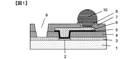
- FIG. 4 is a schematic view of a cross section of a semiconductor package including an IC chip (semiconductor element), rewiring, sealing resin, and an antenna element.
- the photosensitive resin composition of the present invention has a structural unit represented by the general formula (17) and has an ethylenically unsaturated bond, and is a polyimide, a polybenzoxazole, a precursor thereof, and a copolymer thereof.
- a photopolymerization initiator (B) hereinafter, may be abbreviated as the component (B)”.
- "-" when “-" is expressed in the present specification, it means that the upper and lower limit numbers are included unless otherwise specified.
- Polyimide and polybenzoxazole are resins having a cyclic structure of an imide ring or an oxazole ring in the main chain structure. Further, the polyimide precursor and the polybenzoxazole precursor, which are their precursors, are resins that form an imide ring and a benzoxazole ring structure by dehydration ring closure, respectively.
- Polyimide can be obtained by reacting tetracarboxylic acid, tetracarboxylic acid dianhydride, tetracarboxylic acid diester dichloride, etc. with diamine, diisocyanate compound, trimethylsilylated diamine, etc., and tetracarboxylic acid residue and diamine residue.
- a polyimide can be obtained by dehydrating and ring-closing polyamic acid, which is one of the polyimide precursors obtained by reacting tetracarboxylic acid dianhydride with diamine, by heat treatment. During this heat treatment, a solvent that azeotropes with water, such as m-xylene, can also be added.
- a dehydration condensing agent such as carboxylic acid anhydride or dicyclohexylcarbodiimide or a ring-closing catalyst such as a base such as triethylamine can be added to dehydrate and ring-close the ring by chemical heat treatment.
- a weakly acidic carboxylic acid compound can be added to dehydrate and ring closure by heat treatment at a low temperature of 100 ° C. or lower.
- reaction time can be adjusted in the process of dehydration ring closure, or a copolymer can be obtained by polymerizing the polyimide and then continuously polymerizing the polyamic acid.
- tetracarboxylic dianhydride known ones can be used.
- Anhydride 3,3', 4,4'-diphenylsulfonetetracarboxylic dianhydride, 4,4'-oxydiphthalic anhydride, P-phenylenebis (trimeritate anhydride), ethylene glycol bisanhydrotrimeritate , 4,4'-(hexafluoroisopropylidene) diphthalic anhydride and the like. These compounds may be used alone or in combination of two or more.
- diamine a known diamine can be used.
- a known diamine can be used.
- Polybenzoxazole can be obtained by reacting a bisaminophenol compound with a dicarboxylic acid, a dicarboxylic acid chloride, a dicarboxylic acid active ester, etc., and has a dicarboxylic acid residue and a bisaminophenol residue.
- polybenzoxazole can be obtained by dehydrating and closing the ring of polyhydroxyamide, which is one of the polybenzoxazole precursors obtained by reacting a bisaminophenol compound with a dicarboxylic acid, by heat treatment.
- anhydrous phosphoric acid, a base, a carbodiimide compound, or the like can be added to dehydrate and close the ring by chemical treatment.
- copolymer by adjusting the reaction time in the process of dehydration and ring closure, or by polymerizing polybenzoxazole and then continuously polymerizing polyhydroxyamide.
- dicarboxylic acid a known one can be used.
- terephthalic acid isophthalic acid
- diphenyl ether dicarboxylic acid bis (carboxyphenyl) hexafluoropropane
- biphenyl dicarboxylic acid benzophenone dicarboxylic acid
- triphenyl dicarboxylic acid etc.
- tricarboxylic acids include trimeric acid, trimesic acid, diphenyl ether tricarboxylic acid. Acids, biphenyltricarboxylic acids and the like can be mentioned. These compounds may be used alone or in combination of two or more.
- a known bisaminophenol compound can be used.
- a copolymer composed of two or more of polyimide, polybenzoxazole, polyimide precursor, and polybenzoxazole precursor can be obtained.
- the precursor has a bond derived from an ethylenically unsaturated bond even after imidization or oxazoleization.
- a method of introducing an ethylenically unsaturated bond into a resin there is a method of reacting a hydroxyl group and / or a carboxy group in the resin with a compound having an ethylenically unsaturated double bond group, or an ethylenically unsaturated bond.
- Known methods such as a method of obtaining a resin by polymerization using the above-mentioned monomer can be mentioned.
- the compound having an ethylenically unsaturated double bond group an electrophilic compound having an ethylenically unsaturated double bond group is preferable from the viewpoint of reactivity.
- Examples of the electrophilic compound include isocyanate compounds, isothiocyanate compounds, epoxy compounds, aldehyde compounds, thioaldehyde compounds, ketone compounds, thioketone compounds, acetate compounds, carboxylated products, carboxylic acid anhydrides, and carboxylic acid active ester compounds.
- Compounds, epoxy compounds, aldehyde compounds, ketone compounds or carboxylic acid anhydrides are preferable, and isocyanate compounds, epoxy compounds and carboxylic acid anhydrides are more preferable.
- a small amount of a polymerization inhibitor may be used for the purpose of preventing the ethylenically unsaturated bond site from being crosslinked during the reaction.
- the polymerization inhibitor include phenol compounds such as hydroquinone, 4-methoxyphenol, t-butylpyrocatechol, and bis-t-butylhydroxytoluene.
- the amount of the polymerization inhibitor added is preferably 0.1 mol% or more and 5 mol% or less of the phenolic hydroxyl group of the polymerization inhibitor with respect to the ethylenically unsaturated bond of alcohols.
- Formula (17) has a structure having a skeleton of dimer acid, which is a dimer of an unsaturated fatty acid such as linoleic acid or oleic acid, and a structure containing no double bond is preferable from the viewpoint of reliability of the obtained cured film. ..
- diamine having the structure represented by the formula (17) examples include “" Versamine (registered trademark) "551” and “" Versamine (registered trademark) "552 manufactured by BASF Ltd. as commercial products of Dimerdiamine. , “" Priamine (registered trademark) “1073”, “” Priamine (registered trademark) "1074", “” Priamine (registered trademark) "1075" manufactured by Claude Japan Co., Ltd. and the like.
- "" Versamine (registered trademark) "551” and “” Priamine (registered trademark) "1074" are both dimerdiamine compounds containing a compound represented by the formula (10), and “" Versamine (registered trademark) ". ) "552", “Priamine (registered trademark)” 1073 “, and” “Priamine (registered trademark)” 1075 "are all dimerdiamine compounds containing the compound represented by the formula (9).
- trimertriamine and dimerdiamine may be used.
- examples of commercially available products of trimertriamine and dimerdiamine include "" Priamine (registered trademark) "1071” manufactured by Croda Japan Co., Ltd.
- polyvalent carboxylic acid having the structure represented by the formula (17) are "" Pripole (registered trademark) “1009”, “" Pripole (registered trademark) "1006", and “" "Pripole (registered trademark)” 1010 "" “Pripole (registered trademark)” 1013 “,” “Pripole (registered trademark)” 1025 “,” “Pripole (registered trademark)” 1017 “,” “Pripole (registered trademark)” 1040 , "" Puripole (registered trademark) "1004" and the like.
- Examples of the derivative of the polyvalent carboxylic acid having the structure represented by the formula (17) include a reaction product of the dimer diamines exemplified above and trimellitic anhydride chloride. More specifically, it is represented by the equation (11).
- the wavy line means a carbon-carbon single bond or a carbon-carbon double bond.
- the content of the structural unit represented by the formula (17) is preferably 1 mol% or more and 30 mol% or less, more preferably 1 mol% or more and 15 mol% or less.
- the relative permittivity and the dielectric loss tangent can be lowered.
- the heat resistance can be increased by setting the content to 30 mol% or less.
- the photosensitive resin composition of the present invention has at least one of the structural units represented by the formulas (18), (19) and (20), and the resin having the structural unit represented by the formula (17).
- (A2) (hereinafter, may be abbreviated as "(A2) component"), contains a photopolymerization initiator (B).
- X 8 represents a 4- to 6-valent organic group having 2 to 60 carbon atoms
- Y 8 represents a 2- to 6-valent organic group having 2 to 70 carbon atoms
- a plurality of R 19 and R. 20 each independently represents a monovalent organic group having 3 to 30 carbon atoms having a carboxyl group, a hydroxyl group or an ethylenically unsaturated bond
- at least one of R 19 and R 20 is a carbon having an ethylenically unsaturated bond.
- the number 3 to 30 indicates a monovalent organic group
- g indicates an integer of 0 to 2
- h indicates an integer of 0 to 4, 1 ⁇ g + h ⁇ 6, and * indicates a bonding point.
- X 9 represents a 4- to 6-valent organic group having 2 to 60 carbon atoms
- Y 9 represents a 2- to 6-valent organic group having 2 to 70 carbon atoms
- a plurality of R 21 and R. 22 may be the same or different, respectively, and represents a monovalent organic group having 3 to 30 carbon atoms having a carboxyl group, a hydroxyl group or an ethylenically unsaturated bond, and at least one of R 21 and R 22 is ethylenically unsaturated.
- It represents a monovalent organic group having a saturated bond and having 3 to 30 carbon atoms, i represents an integer of 0 to 2, j represents an integer of 0 to 4, 1 ⁇ i + j ⁇ 6, and * is a bond point. Is shown.
- X 10 represents a 4- to 6-valent organic group having 2 to 60 carbon atoms
- Y 10 represents a 2- to 6-valent organic group having 2 to 70 carbon atoms
- (COOR 23 ) is. It is a substituent at a position capable of forming an imide ring with an amide group that binds to X 10
- R 23 indicates a hydrogen atom or an organic group having 1 to 5 carbon atoms
- R 24 is a hydroxyl group or 3 to 30 carbon atoms.
- R 25 represents a carboxyl group, a hydroxyl group or a monovalent organic group having an ethylenically unsaturated bond having 3 to 30 carbon atoms
- R 24 and R 25 At least one of them represents a monovalent organic group having 3 to 30 carbon atoms having an ethylenically unsaturated bond
- k represents an integer of 0 to 2
- x represents an integer of 0 to 2
- y represents 0 to. It indicates an integer of 4, 1 ⁇ x + y ⁇ 6, and * indicates a coupling point.
- the organic group is a group containing at least a carbon atom, and can further contain an oxygen atom, a hydrogen atom, a fluorine atom, and other atoms as needed.
- the X-valent organic group is a group having a chemical structure formed by the organic compound in the form of an X-valent group, and refers to an atomic group obtained by removing X hydrogen atoms from the organic compound.
- the cured film of the present invention obtained by curing the photosensitive resin composition of the present invention has a low dielectric constant and a low dielectric loss tangent.
- the acid component include tetracarboxylic acid, tetracarboxylic dianhydride, and tetracarboxylic acid diester dichloride.
- Y 8 , Y 9 and Y 10 represent divalent organic groups having 2 to 70 carbon atoms and indicate amine residues.
- the content of the structural unit represented by the formula (17) is preferably 1 mol% or more and 30 mol% or less, more preferably 1 mol% or more and 15 mol% or less.
- the relative permittivity and the dielectric loss tangent can be lowered.
- the above equations can increase the heat resistance (18), R 19 and R 20 or formula (19), R 21 and R 22 or an expression (20)
- By having an ethylenically unsaturated bond at any of the positions of R 24 and R 25 it is possible to improve the heat resistance by cross-linking the resins during curing.
- a method of introducing an ethylenically unsaturated bond into a resin there is a method of reacting a hydroxyl group and / or a carboxy group in the resin with a compound having an ethylenically unsaturated double bond group, or an ethylenically unsaturated bond.
- Known methods such as a method of obtaining a resin by polymerization using the above-mentioned monomer can be mentioned.
- the compound having an ethylenically unsaturated double bond group an electrophilic compound having an ethylenically unsaturated double bond group is preferable from the viewpoint of reactivity.
- Examples of the electrophilic compound include isocyanate compounds, isothiocyanate compounds, epoxy compounds, aldehyde compounds, thioaldehyde compounds, ketone compounds, thioketone compounds, acetate compounds, carboxylated products, carboxylic acid anhydrides, and carboxylic acid active ester compounds.
- Compounds, epoxy compounds, aldehyde compounds, ketone compounds or carboxylic acid anhydrides are preferable, and isocyanate compounds, epoxy compounds and carboxylic acid anhydrides are more preferable.
- a small amount of a polymerization inhibitor may be used for the purpose of preventing the ethylenically unsaturated bond site from being crosslinked during the reaction.
- the polymerization inhibitor include phenol compounds such as hydroquinone, 4-methoxyphenol, t-butylpyrocatechol, and bis-t-butylhydroxytoluene.
- the amount of the polymerization inhibitor added is preferably 0.1 mol% or more and 5 mol% or less of the phenolic hydroxyl group of the polymerization inhibitor with respect to the ethylenically unsaturated bond of alcohols.
- the photosensitive resin composition of the present invention contains one or more structural units selected from the group consisting of structural units represented by the formulas (1), (3) and (5), and further comprises the structural units of the formula (1), the formula (3) and the formula (5).
- Resin (A3) containing one or more types of structural units selected from the group consisting of structural units represented by 2), formula (4) and formula (6) (hereinafter abbreviated as "component (A3)") ), Containing a photopolymerization initiator (B).
- X 1 represents a tetravalent organic group having 2 to 60 carbon atoms
- Y 1 represents a divalent organic group having 2 to 70 carbon atoms
- at least one of X 1 and Y 1 is used.
- at least 4 or more hydrogen atoms are substituted with hydrocarbon groups having 4 to 12 carbon atoms which may have unsaturated bonds, and * indicates a bond point.
- X 2 represents a 4- to 6-valent organic group having 2 to 60 carbon atoms
- Y 2 represents a 2- to 6-valent organic group having 2 to 70 carbon atoms
- a plurality of R 1 and R. 2 each independently represents a monovalent organic group having 3 to 30 carbon atoms having a carboxyl group, a hydroxyl group or an ethylenically unsaturated bond, and at least one of R 1 and R 2 is a carbon having an ethylenically unsaturated bond. It indicates a monovalent organic group of the number 3 to 30, p indicates an integer of 0 to 2, q indicates an integer of 0 to 4, 1 ⁇ p + q ⁇ 6, and * indicates a bonding point.
- X 3 represents a tetravalent organic group having 2 to 60 carbon atoms
- Y 3 represents a divalent organic group having 2 to 70 carbon atoms
- at least one of X 3 and Y 3 Indicates a polyvalent carboxylic acid residue and / or a polyvalent amine residue having an alicyclic hydrocarbon structure having 4 to 8 carbon atoms which may have an unsaturated bond, and the alicyclic hydrocarbon.
- at least 4 or more hydrogen atoms are substituted with hydrocarbon groups having 4 to 12 carbon atoms which may have unsaturated bonds, and * indicates a bond point.
- X 4 represents a 4- to 6-valent organic group having 2 to 60 carbon atoms
- Y 4 represents a 2- to 6-valent organic group having 2 to 70 carbon atoms
- a plurality of R 3 and R. 4 may be the same or different, respectively, and represents a monovalent organic group having 3 to 30 carbon atoms having a carboxyl group, a hydroxyl group or an ethylenically unsaturated bond, and at least one of R 3 and R 4 is ethylenically unsaturated.
- X 5 represents a tetravalent organic group having 2 to 60 carbon atoms
- Y 5 represents a divalent organic group having 2 to 70 carbon atoms
- at least one of X 5 and Y 5 Indicates a polyvalent carboxylic acid residue and / or a polyvalent amine residue having an alicyclic hydrocarbon structure having 4 to 8 carbon atoms which may have an unsaturated bond, and the alicyclic hydrocarbon.
- at least 4 or more hydrogen atoms are substituted with hydrocarbon groups having 4 to 12 carbon atoms which may have unsaturated bonds
- (COOR 5 ) is an amide group which binds to X 5. It is a substituent at a position capable of forming an imide ring, R 5 indicates a hydrogen atom or an organic group having 1 to 5 carbon atoms, and * indicates a bonding point.
- X 6 represents a 4- to 6-valent organic group having 2 to 60 carbon atoms
- Y 6 represents a 2- to 6-valent organic group having 2 to 70 carbon atoms
- (COOR 6 ) is. It is a substituent located at a position capable of forming an imide ring with an amide group that binds to X 6
- R 6 represents a hydrogen atom or an organic group having 1 to 5 carbon atoms
- R 7 is a hydroxyl group or 3 to 30 carbon atoms.
- R 8 represents a carboxyl group, a hydroxyl group or a monovalent organic group having an ethylenically unsaturated bond having 3 to 30 carbon atoms
- R 7 and R 8 show. At least one of them has an ethylenically unsaturated bond having 3 to 30 carbon atoms
- t represents an integer of 0 to 2
- u represents an integer of 0 to 4
- * is Indicates the connection point.
- the cured film of the present invention obtained by curing the photosensitive resin composition of the present invention has a low dielectric constant and a low dielectric loss tangent.
- X 1, X 3 and X 5 represents a tetravalent organic group having 2 to 60 carbon atoms, a residue of an acid component.
- the acid component include tetracarboxylic acid, tetracarboxylic dianhydride, and tetracarboxylic acid diester dichloride.
- Y 1 , Y 3 and Y 5 represent divalent organic groups having 2 to 70 carbon atoms and indicate amine residues.
- At least one of X 1 and Y 1 may have a structure of an alicyclic hydrocarbon having 4 to 8 carbon atoms which may have an unsaturated bond (hereinafter, may be abbreviated as “structure (a)”). ), which indicates a polyvalent carboxylic acid residue and / or a polyvalent amine residue, and in the structure of the alicyclic hydrocarbon, at least four or more hydrogen atoms may have an unsaturated bond. It is substituted with a hydrocarbon group of number 4-12.
- At least one of X 3 and Y 3 may have a structure of an alicyclic hydrocarbon having 4 to 8 carbon atoms which may have an unsaturated bond (hereinafter, may be abbreviated as “structure (a)”). ), which indicates a polyvalent carboxylic acid residue and / or a polyvalent amine residue, and in the structure of the alicyclic hydrocarbon, at least four or more hydrogen atoms may have an unsaturated bond. It is substituted with a hydrocarbon group of number 4-12.
- At least one of X 5 and Y 5 may have a structure of an alicyclic hydrocarbon having 4 to 8 carbon atoms which may have an unsaturated bond (hereinafter, may be abbreviated as “structure (a)”). ), which indicates a polyvalent carboxylic acid residue and / or a polyvalent amine residue, and in the structure of the alicyclic hydrocarbon, at least four or more hydrogen atoms may have an unsaturated bond. It is substituted with a hydrocarbon group of number 4-12.
- the cured film obtained by curing the resin composition has high elongation, low dielectric constant, and low dielectric loss tangent.
- Examples of the structure (a) include a cyclobutyl group, a cyclobutenyl group, a cyclopentyl group, a cyclopentenyl group, a cyclohexyl group, a cyclohexenyl group, a cycloheptyl group, a cycloheptenyl group, a cyclooctyl group, a cyclooctenyl group and the like.
- a cyclohexyl group, a cyclohexenyl group, a cycloheptyl group, and a cycloheptenyl group are preferable from the viewpoint of thermal stability.
- hydrocarbon group having 4 to 12 carbon atoms which may have an unsaturated bond examples include an n-butyl group, an i-butyl group, a t-butyl group, a 1-butenyl group, a 2-butenyl group and an n-pentyl group.
- I-pentyl group 1-pentenyl group, 2-pentenyl group, n-hexyl group, i-hexyl group, 1-hexenyl group, 2-hexenyl group, n-heptyl group, i-heptyl group, 1- Heptenyl group, 2-heptenyl group, n-octyl group, i-octyl group, 1-octenyl group, 2-octenyl group, nonyl group, 1-nonenyl group, decanyl group, 1-decenyl group, undecanyl group, 1-undecenyl group Examples include a group, a dodecanyl group, a 1-dodecenyl group and the like.
- Examples of the carboxylic acid compound that becomes a polyvalent carboxylic acid residue include tetracarboxylic acid and hexacarboxylic acid octacarboxylic acid, and examples of the amine compound that becomes a polyvalent amine residue include diamine, triamine, and tetraamine.
- Y 1, Y 3 and Y 5 having the structure (a) is a diamine having the structure (a), derived from a triamine or a residue of a derivative thereof. Further, by using the amino compound corresponding to the polyvalent amine residue at the time of polymerization, these polyvalent amine residues can be included in the structural unit.
- the residue of the polyvalent amine having the structure (a) the residue of the polyvalent amine represented by the formula (7) is preferable from the viewpoint of the reliability of the obtained cured film, and the formula does not contain a double bond.
- the residue of diamine represented by (8) is more preferable.
- the residue of the diamine represented by the formula (9) is particularly preferable from the viewpoint of the economic efficiency of the diamine and the elongation of the obtained cured film.
- l represents an integer of 4 to 8
- W independently represents any of the structural units represented by formulas (7a), (7b) or (7c).
- the sum of the numbers of (7b) and (7c) is 4 or more and 8 or less
- m and n are independently 3 to 11 respectively. Indicates one of the integers of.
- the wavy line means a carbon-carbon single bond or a carbon-carbon double bond. However, at least one in one molecule shows a double bond.
- polyvalent amine having the structure (a) examples include "" Versamine (registered trademark) "551” and “" Versamine (registered trademark) "552" (above, products) as commercially available products of dimerdiamine and trimertriamine. Name (manufactured by BASF Co., Ltd.), "" Priamine (registered trademark) “1071”, “” Priamine (registered trademark) “1073”, “” Priamine (registered trademark) "1074", "” Priamine (registered trademark) " Examples include “1075" (above, trade name (manufactured by Crowder Japan Co., Ltd.)).
- X 1 , X 3 and X 5 having the structure (a) are derived from the residue of the polyvalent carboxylic acid residue having the structure (a) or a derivative thereof. Further, by using the acid component corresponding to the polyvalent carboxylic acid residue at the time of polymerization, these acid residues can be included in the structural unit. Structure The residue of the polyvalent carboxylic acid having (a), the reaction product of Y 1, Y 3 and polyvalent amines with trimellitic anhydride acid chloride exemplified in Y 5 having the above structure (a) Residues are mentioned. More specifically, the residue of the formula (11) can be mentioned.
- a method of introducing an ethylenically unsaturated bond into a resin there is a method of reacting a hydroxyl group and / or a carboxy group in the resin with a compound having an ethylenically unsaturated double bond group, or an ethylenically unsaturated bond.
- Known methods such as a method of obtaining a resin by polymerization using the above-mentioned monomer can be mentioned.
- the compound having an ethylenically unsaturated double bond group an electrophilic compound having an ethylenically unsaturated double bond group is preferable from the viewpoint of reactivity.
- Examples of the electrophilic compound include isocyanate compounds, isothiocyanate compounds, epoxy compounds, aldehyde compounds, thioaldehyde compounds, ketone compounds, thioketone compounds, acetate compounds, carboxylated products, carboxylic acid anhydrides, and carboxylic acid active ester compounds.
- Compounds, epoxy compounds, aldehyde compounds, ketone compounds or carboxylic acid anhydrides are preferable, and isocyanate compounds, epoxy compounds and carboxylic acid anhydrides are more preferable.
- a small amount of a polymerization inhibitor may be used for the purpose of preventing the ethylenically unsaturated bond site from being crosslinked during the reaction.
- the polymerization inhibitor include phenol compounds such as hydroquinone, 4-methoxyphenol, t-butylpyrocatechol, and bis-t-butylhydroxytoluene.
- the amount of the polymerization inhibitor added is preferably 0.1 mol% or more and 5 mol% or less of the phenolic hydroxyl group of the polymerization inhibitor with respect to the ethylenically unsaturated bond of alcohols.
- the resin (A3) contains a structural unit represented by the formula (2), at least one of a plurality of R 1 and R 2 is a group represented by the formula (12) or the formula (13).
- the resin (A3) contains a structural unit represented by the formula (4), at least one of a plurality of R 3 and R 4 is a group represented by the formula (12) or the formula (13).
- the resin (A3) contains a structural unit represented by the formula (6)
- at least one of a plurality of R 7 and R 8 is a group represented by the formula (12) or the formula (13). Is preferable.
- R 9 represents a linking group represented by -OCH 2 CH (OH)-, -OCONH-, -NHCH 2 CH (OH)-, or -NHCONH-, R 10 , R 11 , and.
- R 12 represents a hydrogen atom, a methyl group, an ethyl group or a propyl group, respectively, a represents an integer of 1 to 10, and * represents a bonding point.
- R 9 is preferably -OCONH- or -NHCONH- because of the ease of introducing the group into the resin (A3).
- R 13 represents a linking group represented by -OCO- or -NHCO-
- R 14 , R 15 and R 16 are either hydrogen atoms, methyl groups, ethyl groups or propyl groups, respectively.
- B indicates an integer from 0 to 10, and * indicates a connection point.
- a heat-resistant viewpoint of cured film R 13 is -NHCO- is preferred.
- one or more kinds of resins selected from the group consisting of the structural units represented by the formulas (1), (3) and (5) are 1 or more. It is preferably contained in an amount of about 30 mol%, more preferably 1 to 15 mol%. Within the above range, heat resistance can be improved while maintaining a low dielectric constant and a low dielectric loss tangent.
- X 1 to X 6 are composed of a bisphenol A skeleton, a biphenyl skeleton, a hexafluoroisopropylidene skeleton, and an acid anhydride residue represented by the formula (14). Containing any one or more selected, or Y 1 to Y 6 are selected from the group consisting of bisphenol A skeleton, biphenyl skeleton, hexafluoroisopropyrine skeleton and diamine residues represented by formula (15). It is preferable to include any one or more of them.
- z indicates an integer of 6 to 20, and * indicates a connection point.
- Examples of the carboxylic acid compound having an acid anhydride residue represented by a bisphenol A skeleton, a biphenyl skeleton, and a hexafluoroisopropylidene skeleton include 3,3', 4,4'-biphenyltetracarboxylic acid, 2,3.
- 2,2-bis (3,4-dicarboxyphenyl) hexafluoropropane and 2,2-bis (2,3-bis) are considered from the viewpoint of solubility in organic solvents, transparency, and low dielectric constant.
- Dicarboxyphenyl) hexafluoropropane, 4,4'-(4,4'-isopropyridene diphenoxy) bis (phthalic acid) are preferred.
- Examples of the amino compound having a diamine residue represented by a bisphenol A skeleton, a biphenyl skeleton, and a hexafluoroisopropylidene skeleton include 4,4'-diaminobiphenyl and 2,2'-dimethyl-4,4'-diamino.
- Aromatic diamines such as hydroxyphenyl) hexafluoropropane and 2,2-bis [4- (4-aminophenoxy) phenyl] propane, and 1,4-cyclohexanediamine and 1,2-bis in the general formula (15).
- (Aminomethyl) cyclohexane and 1,3-bis (aminomethyl) cyclohexane are preferred.
- Y 1 to Y 6 contain a residue of the diamine represented by the formula (16).
- R 17 and R 18 each independently represent a group selected from a methyl group, a trifluoromethyl group, and a hydroxyl group, and v and w represent integers of 0 to 4.
- amino compounds containing these diamine residues include 2,2'-bis (trifluoromethyl) -4,4'-diaminobiphenyl, 2,2'-dimethylbiphenyl-4,4'-diamine, 3, Examples thereof include 3'-dihydroxybenzidine.
- carboxylic acid compounds that serve as other usable acid residues of X 1 to X 6 and X 8 to X 10 include pyromellitic acid, 3,3', 4,4'-benzophenone tetracarboxylic acid, 2, 2', 3,3'-benzophenone tetracarboxylic acid, 1,1-bis (3,4-dicarboxyphenyl) ethane, 1,1-bis (2,3-dicarboxyphenyl) ethane, bis (3,4) -Dicarboxyphenyl) methane, bis (2,3-dicarboxyphenyl) methane, bis (3,4-dicarboxyphenyl) sulfone, bis (3,4-dicarboxyphenyl) thioether, bis (3,4-dicarboxyphenyl) Carboxylic acid) ether, 1,3-bis (3,4-dicarboxyphenoxy) benzene, trimellitic acid (3,4-dicarboxypheny
- Hept-2-enetetracarboxylic acid bicyclo [2.2.2. ]
- Aliphatic tetracarboxylic acids such as octanetetracarboxylic acid and adamatanetetracarboxylic acid can be mentioned.
- a and D represent a hydrogen atom, a methyl group, an ethyl group, a propyl group, an isopropyl group, a t-butyl group, a trifluoromethyl group, a halogen group, a phenoxy group and a nitro group. * Indicates the connection point.
- a silicon atom-containing tetracarboxylic acid such as dimethylsilanediphthalic acid or 1,3-bis (phthalic acid) tetramethyldisiloxane
- adhesion to a substrate, oxygen plasma used for cleaning, etc. UV ozone
- UV ozone The resistance to treatment can be increased. It is preferable to use 1 to 30 mol% of the total acid component of these silicon atom-containing tetracarboxylic acids.
- Amine compounds that are other usable amine residues of Y 1 to Y 6 and Y 8 to Y 10 include, for example, aromatic diamines such as m-phenylenediamine, p-phenylenediamine, 3,4'-diamino.
- aromatic diamine of the above examples include compounds in which a part of the hydrogen atom of these aromatic rings is replaced with an alkyl group having 1 to 10 carbon atoms, a fluoroalkyl group, a halogen atom, or the like, but are limited thereto. Not done.
- aliphatic diamine examples include ethylenediamine, 1,3-diaminopropane, 2-methyl-1,3-propanediamine, 1,4-diaminobutane, 1,5-diaminopentane, and 2-methyl-1,5-.
- diamine having a siloxane structure examples include bis (3-aminopropyl) tetramethyldisiloxane and bis (p-aminophenyl) octamethylpentasiloxane, which are preferable because they can improve the adhesiveness to the substrate. ..
- the above diamine compound can be used as it is or as a compound in which the amine moiety is isocyanated or trimethylsilylated. Further, these two or more kinds of diamine compounds may be used in combination.
- a fluorine component in the structure of the resin (A1), the resin (A2) or the resin (A3). And has a fluorine component, it is to include an organic group having a fluorine atom in its structure, any of X 1 ⁇ X 6 and X 8 ⁇ X 10 or Y 1 ⁇ Y 6 and Y 8 ⁇ Y 10, It preferably contains an organic group having a fluorine atom.
- Known methods for introducing a fluorine component include a method of obtaining a resin by polymerizing using a monomer having a fluorine atom, and a method of reacting a hydroxyl group and / or a carboxy group in the resin with a compound having a fluorine atom. The method can be mentioned.
- the compound having a fluorine atom examples include 2,2-bis (3,4-dicarboxyphenyl) hexafluoropropane dianhydride or a compound in which the aromatic rings thereof are replaced with an alkyl group or a halogen atom.
- aromatic acid dianhydrides such as acid dianhydrides with amide groups, bis (3-amino-4-hydroxyphenyl) hexafluoropropane,
- Aromatic diamines such as 2,2'-bis (trifluoromethyl) -4,4'-diaminobiphenyl and some of the hydrogen atoms of these aromatic rings can be used as alkyl groups with 1 to 10 carbon atoms or fluoroalkyl. Examples thereof include compounds substituted with groups and halogen atoms.
- Fluorine has a large atomic radius and has the effect of expanding the free volume, so the relative permittivity and dielectric loss tangent can be lowered.
- the organic group having a fluorine atom is preferably 30 mol% or more with respect to 100 mol% of the total structural unit of the resin (A1), the resin (A2) or the resin (A3). Further, in order to obtain adhesion to the substrate, the organic group having a fluorine atom is preferably 90 mol% or less. Twice
- X 1 to X 6 and X 8 to X 10 or Y 1 to Y 6 and Y 8 to Y 10 is an organic group having a phenolic hydroxyl group. Phenolic hydroxyl groups can be obtained with high mechanical properties and chemical resistance due to the improvement of heat resistance due to hydrogen bond interaction and the contribution of the reaction with the cross-linking agent.
- Having a phenolic hydroxyl group as a polar group tends to worsen the dielectric loss tangent, but 1 to 25 mol with respect to 100 mol% of the total structural unit of the resin (A1), the resin (A2) or the resin (A3). If it is%, the mechanical properties and chemical resistance can be improved without deteriorating the dielectric loss tangent. More preferably, it is 1 to 15 mol%.
- the compound having a phenolic hydroxyl group examples include 2,2-bis (3,4-dicarboxyphenyl) hexafluoropropane dianhydride or a compound in which the aromatic rings thereof are replaced with an alkyl group or a halogen atom.
- aromatic acid dianhydrides such as acid dianhydride having an amide group, bis (3-amino-4-hydroxyphenyl) hexafluoropropane, bis (3-amino-4-hydroxyphenyl) sulfone, bis ( 3-Amino-4-hydroxyphenyl) propane, bis (3-amino-4-hydroxyphenyl) methylene, bis (3-amino-4-hydroxyphenyl) ether, bis (3-amino-4-hydroxy) biphenyl, bis Hydroxy group-containing diamines such as (3-amino-4-hydroxyphenyl) fluorene and some of the hydrogen atoms of these aromatic rings are replaced with alkyl groups having 1 to 10 carbon atoms, fluoroalkyl groups, halogen atoms, and the like. Compounds, etc. can be mentioned.
- the main chain ends of the components (A1) to (A3) may be sealed with an end-capping agent.
- the terminal encapsulant include monoamine, acid anhydride, monocarboxylic acid, monoacid chloride compound, monoactive ester compound and the like.
- an end-capping agent having a hydroxyl group, a carboxyl group, a sulfonic acid group, a thiol group, a vinyl group, an ethynyl group, a maleimide group or an allyl group, the exposure sensitivity of the cured film obtained can be obtained.
- the mechanical properties and the like can be easily adjusted within a preferable range.
- the introduction ratio of the end sealant is preferably 0.1 mol% or more and 60 mol% or less, and particularly preferably 5 mol% or more and 50 mol% or less, from the viewpoint of solubility in a developing solution and mechanical properties of the obtained cured film.
- a plurality of end sealants may be reacted to introduce a plurality of different end groups.
- Known compounds can be used as the monoamine used for the terminal encapsulant, but aniline, 2-ethynylaniline, 3-ethynylaniline, 4-ethynylaniline, 1-hydroxy-7-aminonaphthalene, 1-carboxy-7 -Aminonaphthalene, 3-aminobenzoic acid, 3-aminophenol, 3-aminothiophenol, etc. are preferable. Two or more of these may be used.
- Known compounds can be used as the acid anhydride, monocarboxylic acid, monoacid chloride compound, and monoactive ester compound, but phthalic anhydride, maleic anhydride, nadic acid anhydride, cyclohexanedicarboxylic acid anhydride, 3 -Acid anhydrides such as hydroxyphthalic anhydride, itaconic acid anhydride and the like are preferable. Maleic anhydride and itaconic anhydride are particularly preferable. Two or more of these may be used.
- the components (A1) to (A3) in the present invention preferably have a weight average molecular weight of 5,000 or more and 100,000 or less.
- a weight average molecular weight 5,000 or more and 100,000 or less.
- GPC gel permeation chromatography
- the photosensitive resin composition of the present invention contains (B) a photopolymerization initiator.
- (B) By containing the photopolymerization initiator, pattern processing becomes possible through the exposure and development steps.
- the photopolymerization initiator (B) is not particularly limited as long as it is a compound that generates radicals upon exposure, but is an alkylphenone compound, an aminobenzophenone compound, a diketone compound, a ketoester compound, a phosphine oxide compound, an oxime ester compound, and a benzoic acid ester.
- the compound is preferable because it has excellent sensitivity, stability, and ease of synthesis.
- an alkylphenone compound and an oxime ester compound are preferable from the viewpoint of sensitivity, and an oxime ester compound is particularly preferable. Further, in the case of a thick film having a processed film thickness of 5 ⁇ m or more, a phosphine oxide compound is preferable from the viewpoint of resolution.
- alkylphenone compound examples include 2-methyl- [4- (methylthio) phenyl] -2-morpholinopropan-1-one and 2-dimethylamino-2- (4-methylbenzyl) -1- (4-).
- ⁇ -Aminoalkylphenone compounds such as morpholin-4-yl-phenyl) -butane-1-one, ⁇ -hydroxyalkylphenone compounds such as 1-hydroxycyclohexyl-phenylketone and benzoin, 4-benzoyl-4-methylphenyl
- ⁇ -alkoxyalkylphenylone compounds such as ketones and 2,3-diethoxyacetophenone.
- the ⁇ -aminoalkylphenone compound is preferable because of its high sensitivity.
- Examples of the phosphine oxide compound include 6-trimethylbenzoylphenylphosphine oxide.
- Examples of the oxime ester compound include 1- [9-ethyl-6- (2-methylbenzoyl) -9H-carbazole-3-yl]-, 1- (0-acetyloxime), 2-octanedione, 1-. [4- (Phenylthio) -2- (O-benzoyloxime)], NCI-831, NCI-930 (trade name, manufactured by ADEKA Co., Ltd.), "Irgacure (registered trademark)" OXE-03, OXE- 04 (above, trade name, manufactured by BASF Co., Ltd.) can be mentioned.
- aminobenzophenone compound examples include 4,4-bis (dimethylamino) benzophenone.
- diketone compound examples include benzyl.
- ketoester compound examples include methyl benzoylate.
- benzoic acid ester compound examples include methyl o-benzoyl benzoate and ethyl p-dimethylaminobenzoate.
- photopolymerization initiator examples include benzophenone, 4-benzoyl-4'-methyldiphenylketone, dibenzylketone, fluorenone, thioxanthone, 2-methylthioxanthone, 2-isopropylthioxanthone, 2-hydroxy-. 3- (3,4-dimethyl-9-oxo-9H-thioxanthen-2-yloxy) -N, N, N-trimethyl-1-propanaminium chloride, anthraquinone, triphenylphosphine, carbon tetrabromide, etc. Can be mentioned.
- the content of the photopolymerization initiator (B) is 0 when the sum of the components (A1) to (A3) and the compound having two or more ethylenically unsaturated bonds contained as needed is 100 parts by mass. 5.5 parts by mass or more and 20 parts by mass or less are preferable because sufficient sensitivity can be obtained and the amount of degassing during heat curing can be suppressed. Above all, 1.0 part by mass or more and 10 parts by mass or less are more preferable.
- the photosensitive resin composition of the present invention may contain a sensitizer for the purpose of enhancing the function of (B) the photopolymerization initiator.
- a sensitizer for the purpose of enhancing the function of (B) the photopolymerization initiator.
- the sensitizer include bis (dimethylamino) benzophenone, bis (diethylamino) benzophenone, diethylthioxanthone, N-phenyldiethanolamine, N-phenylglycine, 7-diethylamino-3-benzoylcoumarin, 7-diethylamino-4-methylcoumarin, Examples include, but are not limited to, N-phenylmorpholine and derivatives thereof.
- the photosensitive resin composition of the present invention further contains a compound (C) having two or more ethylenically unsaturated bonds and an alicyclic structure (hereinafter, may be abbreviated as "component (C)").
- component (C) a compound having two or more ethylenically unsaturated bonds and an alicyclic structure
- component (C) a compound having two or more ethylenically unsaturated bonds and an alicyclic structure
- component (C) a compound having two or more ethylenically unsaturated bonds and an alicyclic structure
- Examples of the polyfunctional (meth) acrylate containing an alicyclic structure include dimethylol-tricyclodecanedi (meth) acrylate, 1,3-adamantane di (meth) acrylate, and 1,3,5-adamantane trioldi (meth). Meta) acrylate, 1,3,5-adamantane trioltri (meth) acrylate, 1,4-cyclohexanedimethanol di (meth) acrylate, 5-hydroxy-1,3-adamantane (meth) acrylate, EO-modified hydrogenated Examples thereof include bisphenol A di (meth) acrylate.
- the content of the component (C) is preferably 5 parts by mass or more and 100 parts by mass or less, and more preferably 10 parts by mass or more and 40 parts by mass or less with respect to 100 parts by mass of the components (A1) to (A3). Within such a range, the effect of improving the exposure sensitivity, the low dielectric constant, and the low dielectric loss tangent can be easily obtained.
- the photosensitive resin composition of the present invention may contain a known (meth) acrylate compound in addition to the component (C).
- polyfunctional (meth) acrylate examples include diethylene glycol di (meth) acrylate, trimethylolpropane tri (meth) acrylate, 1,3-butanediol di (meth) acrylate, neopentyl glycol di (meth) acrylate, 1, 4-Butandiol di (meth) acrylate, 1,6-hexanediol di (meth) acrylate, pentaerythritol tetra (meth) acrylate, ethoxylated bisphenol A di (meth) acrylate, 9,9-bis [4- (2) -(Meta) acryloyloxyethoxy) phenyl] fluorene and the like.
- Examples of other polyfunctional (meth) acrylate compounds include epoxy (meth) acrylate obtained by reacting a polyfunctional epoxy compound with (meth) acrylic acid. Since epoxy (meth) acrylate adds hydrophilicity, it can be used for the purpose of improving alkali developability. These polyfunctional epoxy compounds are preferable because they have excellent heat resistance and chemical resistance.
- the photosensitive resin composition of the present invention preferably contains a thermal cross-linking agent (D) (hereinafter, may be abbreviated as "component (D)”).
- component (D) thermal cross-linking agent
- thermal cross-linking agent examples include a compound having an epoxy structure, a compound having a hydroxymethyl structure, and a compound having an alkoxymethyl structure.
- a known compound can be contained as a compound having an epoxy structure.
- Known compounds having a hydroxymethyl structure and compounds having an alkoxymethyl structure can be contained.
- DML-PC, TMOM-BPAP, HML-TPPHBA, HML-TPHAP, HMOM-TPPHBA, HMOM-TPHAP trade name, available from Honshu Chemical Industry Co., Ltd.
- TMOM-BPAP NIKALAC MX-290, NIKALAC MX-280, NIKALAC MX-270, NIKALAC MX-279, NIKALAC from the viewpoint of heat resistance and chemical resistance of the cured film and storage stability. It is preferable that the compound is selected from any of MW-100LM and NIKALAC MX-750LM.
- the amount of the thermal cross-linking agent added is preferably 1 part by mass or more and 20.0 parts by mass or less, and more preferably 5 parts by mass or more and 15 parts by mass or less with respect to 100 parts by mass of the components (A1) to (A3). Within such a range, the chemical resistance and heat resistance of the cured film can be improved while maintaining a low dielectric loss tangent.
- the photosensitive resin composition of the present invention may contain an antioxidant.
- an antioxidant By containing the antioxidant, it is possible to suppress deterioration of mechanical properties such as yellowing and elongation of the cured film in the heat treatment in the subsequent process. Further, it is preferable because the rust preventive action on the metal material can suppress the oxidation of the metal material.
- antioxidant a hindered phenol-based antioxidant or a hindered amine-based antioxidant is preferable.
- hindered phenolic antioxidant examples include "Irganox (registered trademark)" 245, 3114, 1010, 1098, 1135, 259, 035 (trade name, manufactured by BASF Ltd.), or 2,6. -Di (t-butyl) -p-cresol, but not limited to these.
- hindered amine-based antioxidant examples include "TINUVIN (registered trademark)" 144, 292, 765, 123 (above, trade name, manufactured by BASF Limited).
- antioxidants include phenol, catechol, resorcinol, hydroquinone, 4-t-butylcatechol, 2,6-di (t-butyl) -p-cresol, phenothiazine, 4-methoxyphenol.
- the amount of the antioxidant added is preferably 0.1 part by mass or more and 10.0 parts by mass or less, and 0.3 parts by mass or more and 5.0 parts by mass with respect to 100 parts by mass of the components (A1) to (A3). Less than a part is more preferable. Within such a range, the developability and the discoloration suppressing effect due to the heat treatment can be appropriately maintained.
- the photosensitive resin composition of the present invention may have a heterocyclic compound containing a nitrogen atom.
- a heterocyclic compound containing a nitrogen atom By having a heterocyclic compound containing a nitrogen atom, high adhesion can be obtained on a substrate of a metal that is easily oxidized such as copper, aluminum, and silver. The mechanism is not clear, but it is presumed that the metal coordination ability of the nitrogen atom interacts with the metal surface, and the bulkiness of the heterocycle stabilizes the interaction.
- heterocyclic compound containing a nitrogen atom examples include imidazole, pyrazole, indazole, carbazole, pyrazoline, pyrazoline, triazole, tetrazole, pyridine, piperidine, pyrimidine, pyrazine, triazine, cyanuric acid, isocyanuric acid and derivatives thereof.
- heterocyclic compound containing a nitrogen atom examples include 1H-benzotriazole, 4-methyl-1H-methylbenzotriazole, 5-methyl-1H-methylbenzotriazole, and 4-carboxy-1H from the viewpoint of reactivity with metals.
- -Benzotriazole, 5-carboxy-1H-benzotriazole, 1H-tetrazole, 5-methyl-1H-tetrazole, 5-phenyl-1H-tetrazole and the like are preferable.
- the amount of the heterocyclic compound containing a nitrogen atom is preferably 0.01 parts by mass or more and 5.0 parts by mass or less, preferably 0.05 parts by mass or more, based on 100 parts by mass of the components (A1) to (A3). More preferably, it is 3.0 parts by mass or less. Within such a range, the developability and the stabilizing effect of the base metal can be appropriately maintained.
- the photosensitive resin composition of the present invention may contain a solvent.
- Solvents include N-methyl-2-pyrrolidone, ⁇ -butyrolactone, ⁇ -valerolactone, ⁇ -valerolactone, N, N-dimethylformamide, N, N-dimethylacetamide, dimethylsulfoxide, N, N'-dimethylpropylene.
- Polar aproton solvents such as urea, N, N-dimethylisobutyric acid amide, methoxy-N, N-dimethylpropionamide, ethers such as tetrahydrofuran, propylene glycol monomethyl ether, propylene glycol monoethyl ether, methyl ethyl ketone, diisobutyl ketone, Ketones such as cyclohexanone, esters such as butyl acetate and propylene glycol monomethyl ether acetate, alcohols such as ethyl lactate, methyl lactate, diacetone alcohol, 3-methyl-3-methoxybutanol, aromatic charcoal such as toluene and xylene. Examples include hydrogens. Two or more of these may be contained.
- the content of the solvent is preferably 100 parts by mass or more in order to dissolve the composition with respect to 100 parts by mass of the components (A1) to (A3), and to form a coating film having a film thickness of 1 ⁇ m or more. It is preferably contained in an amount of 1,500 parts by mass or less.
- the photosensitive resin composition of the present invention may contain a silane coupling agent as a silicon component as long as the storage stability is not impaired.
- a silane coupling agent include trimethoxyaminopropylsilane, trimethoxycyclohexylepoxyethylsilane, trimethoxyvinylsilane, trimethoxythiolpropylsilane, trimethoxyglycidyloxypropylsilane, tris (trimethoxysilylpropyl) isocyanurate, and triethoxyamino.
- Examples thereof include propylsilane and a reaction product of trimethoxyaminopropylsilane and an acid anhydride.
- the reaction product can be used in the state of amic acid or in the state of imidization.
- Examples of the acid anhydride to be reacted include succinic anhydride, maleic anhydride, nadic acid anhydride, cyclohexanedicarboxylic acid anhydride, 3-hydroxyphthalic anhydride, pyromellitic dianhydride, 3,3', 4,4.
- silane coupling agent 0.01 to 10 parts by mass with respect to 100 parts by mass of the components (A1) to (A3).
- the photosensitive sheet of the present invention is completely cured, which is obtained by applying the photosensitive resin composition of the present invention to a substrate and drying it at a temperature and time within a range in which the solvent can be volatilized. It refers to a sheet-like material that is soluble in an organic solvent or an alkaline aqueous solution.
- the base material is not particularly limited, but various commercially available films such as polyethylene terephthalate (PET) film, polyphenylene sulfide film, and polyimide film can be used.
- PET polyethylene terephthalate
- the bonding surface between the base material and the photosensitive resin composition may be subjected to surface treatment such as silicone, silane coupling agent, aluminum chelating agent, polyurea, etc. in order to improve adhesion and peelability.
- the thickness of the base material is not particularly limited, but is preferably in the range of 10 to 100 ⁇ m from the viewpoint of workability.
- a protective film may be provided on the film surface. Thereby, the surface of the photosensitive resin composition can be protected from pollutants such as dust and dust in the atmosphere.
- the photosensitive resin composition As a method of applying the photosensitive resin composition to the substrate, rotary coating using a spinner, spray coating, roll coating, screen printing, blade coater, die coater, calendar coater, meniscus coater, bar coater, roll coater, comma roll Examples include coaters, gravure coaters, screen coaters, and slit die coaters.
- the coating film thickness varies depending on the coating method, the solid content concentration of the composition, the viscosity, etc., but usually, the film thickness after drying is 0.5 ⁇ m or more and 100 ⁇ m or less from the viewpoint of coating film uniformity and the like. preferable.
- the drying temperature and drying time may be any range as long as the solvent can be volatilized, and it is preferable to appropriately set the drying range so that the photosensitive resin composition is in an uncured or semi-cured state. Specifically, it is preferably carried out in the range of 40 ° C. to 150 ° C. for 1 minute to several tens of minutes. Further, these temperatures may be combined to raise the temperature stepwise, and for example, heat treatment may be performed at 80 ° C. and 90 ° C. for 2 minutes each.
- the cured film of the present invention can be obtained by curing a photosensitive resin composition or a photosensitive sheet by heat treatment.
- the heat treatment temperature may be 150 ° C. to 350 ° C.
- a certain temperature is selected and the temperature is raised stepwise, or a certain temperature range is selected and the temperature is continuously raised for 5 minutes to 5 hours.
- heat treatment is performed at 130 ° C. and 200 ° C. for 30 minutes each.
- the lower limit of the cure condition in the present invention is preferably 170 ° C. or higher, but more preferably 180 ° C. or higher in order to sufficiently proceed with curing.
- the upper limit of the cure condition is not particularly limited, but is preferably 280 ° C. or lower, more preferably 250 ° C. or lower, and even more preferably 230 ° C. or lower, from the viewpoint of suppressing film shrinkage and stress.
- the photosensitive resin composition of the present invention is applied onto a substrate, or the photosensitive sheet is laminated on a substrate.
- Metallic copper-plated substrates and silicon wafers are used as the substrates, and ceramics, gallium arsenide, and the like are used as the materials, but the substrate is not limited thereto.
- As a coating method there are methods such as rotary coating using a spinner, spray coating, and roll coating.
- the coating film thickness varies depending on the coating method, the solid content concentration of the composition, the viscosity, and the like, but is usually applied so that the film thickness after drying is 0.1 to 150 ⁇ m.
- the substrate can also be pretreated with the above-mentioned silane coupling agent in order to enhance the adhesiveness between the substrate and the photosensitive resin composition.
- a solution in which a silane coupling agent is dissolved in a solvent such as isopropanol, ethanol, methanol, water, tetrahydrofuran, propylene glycol monomethyl ether acetate, propylene glycol monomethyl ether, ethyl lactate, and diethyl adipate in an amount of 0.5 to 20% by mass is prepared.
- a solution in which a silane coupling agent is dissolved in a solvent such as isopropanol, ethanol, methanol, water, tetrahydrofuran, propylene glycol monomethyl ether acetate, propylene glycol monomethyl ether, ethyl lactate, and diethyl adipate in an amount of 0.5 to 20% by mass is prepared.
- the prepared solution is surface-treated on the substrate by spin coating
- the photosensitive resin composition is applied, or the substrate on which the photosensitive sheet of the present invention is laminated is dried to obtain a photosensitive resin composition film. Drying is preferably carried out in the range of 50 ° C. to 150 ° C. for 1 minute to several hours using an oven, a hot plate, infrared rays or the like. In the case of a photosensitive sheet, it is not always necessary to go through the drying step.
- the photosensitive resin composition film is exposed.
- the chemical beam may be irradiated and exposed through a mask having a desired pattern.
- Chemical rays used for exposure include ultraviolet rays, visible rays, electron beams, X-rays, etc., but in the present invention, it is preferable to use i-rays (365 nm), h-rays (405 nm), and g-rays (436 nm) of mercury lamps. ..
- the exposed photosensitive resin composition film may be subjected to a post-exposure baking (PEB) step, if necessary.
- the PEB step is preferably carried out in the range of 50 ° C. to 150 ° C. for 1 minute to several hours using an oven, a hot plate, infrared rays or the like.
- the photosensitive resin film after exposure is developed.
- a developer is used to remove unexposed areas.
- a good solvent for the photosensitive resin composition or a combination of the good solvent and a poor solvent is preferable.
- a good solvent N-methylpyrrolidone, N, N-dimethylacetamide, cyclopentanone, cyclohexanone, ⁇ -butyrolactone and the like are preferable.
- the poor solvent toluene, xylene, ethanol, isopropyl alcohol, ethyl lactate, propylene glycol methyl ether acetate, water and the like are preferable.
- a good solvent and a poor solvent are mixed and used, it is preferable to adjust the ratio of the poor solvent to the good solvent according to the solubility of the polymer in the photosensitive resin composition. Further, two or more kinds of each solvent, for example, several kinds can be used in combination.
- the alkaline aqueous solution may be developed.
- the developer used for development dissolves and removes an alkaline aqueous solution-soluble polymer, and is typically an alkaline aqueous solution in which an alkaline compound is dissolved.
- the alkaline compound include tetramethylammonium hydroxide, diethanolamine, diethylaminoethanol, sodium hydroxide, potassium hydroxide, sodium carbonate, potassium carbonate and the like.
- these alkaline aqueous solutions may contain polar solvents such as N-methyl-2-pyrrolidone, N, N-dimethylformamide, N, N-dimethylacetamide, dimethylsulfoxide and ⁇ -butyrolactone, methanol, ethanol, isopropanol and the like.
- polar solvents such as N-methyl-2-pyrrolidone, N, N-dimethylformamide, N, N-dimethylacetamide, dimethylsulfoxide and ⁇ -butyrolactone, methanol, ethanol, isopropanol and the like.
- Alcohols, esters such as ethyl lactate and propylene glycol monomethyl ether acetate
- ketones such as cyclopentanone, cyclohexanone and isobutyl ketone may be contained alone or in combination of several kinds.
- an organic solvent or water After development, it is preferable to rinse with an organic solvent or water.
- an organic solvent in addition to the above developer, ethylene glycol monomethyl ether acetate, propylene glycol monomethyl ether acetate and the like can be mentioned.
- water alcohols such as ethanol and isopropyl alcohol, and esters such as ethyl lactate and propylene glycol monomethyl ether acetate may be added to the water for rinsing.
- the developed photosensitive resin film is heat-treated.
- a temperature of 150 ° C. to 350 ° C. is applied to allow the thermal cross-linking reaction to proceed and cure.
- This heat treatment is carried out for 5 minutes to 5 hours while selecting a certain temperature and gradually raising the temperature, or selecting a certain temperature range and continuously raising the temperature.
- heat treatment is performed at 130 ° C. and 200 ° C. for 30 minutes each.
- the lower limit of the cure condition in the present invention is preferably 170 ° C. or higher, but more preferably 180 ° C. or higher in order to sufficiently proceed with curing.
- the upper limit of the cure condition is not particularly limited, but is preferably 280 ° C. or lower, more preferably 250 ° C. or lower, and even more preferably 230 ° C. or lower, from the viewpoint of suppressing film shrinkage and stress.
- the electronic component of the present invention or the display device of the present invention comprises the cured film of the present invention.
- examples of electronic components include active components having semiconductors such as transistors, diodes, integrated circuits (ICs), and memories, and passive components such as resistors, capacitors, and inductors.
- electronic components include a package sealed for the purpose of improving the durability of these components and a module in which a plurality of components are integrated.
- electronic components using semiconductors are also referred to as semiconductor devices or semiconductor packages.
- a display panel and a touch sensor panel can also be mentioned.
- the cured film provided in an electronic component or display device include a semiconductor passivation film, a semiconductor element, a surface protective film such as a TFT (Thin Film Transistor), and a re-layered wiring for high-density mounting of 2 to 10 layers.
- a semiconductor passivation film a semiconductor element
- a surface protective film such as a TFT (Thin Film Transistor)
- a re-layered wiring for high-density mounting of 2 to 10 layers.
- Interlayer insulating film such as interlayer insulating film between wirings, insulating film for touch panel display, protective film, insulating film for organic electroluminescence (hereinafter referred to as EL) element, TFT substrate for driving display device using organic EL element
- EL organic electroluminescence
- TFT substrate for driving display device using organic EL element It is suitably used for applications such as a flattening film, an on-chip microlens of a solid-state imaging device, and a flattening film for various displays and solid-state imaging devices, but the present invention is not limited to this, and various structures can be adopted. Among these, it is preferable to use it as an interlayer insulating film in a multilayer wiring for high-density mounting.
- FIG. 1 is an enlarged cross-sectional view of a pad portion of a semiconductor device having bumps in the present invention.
- a passivation film 3 is formed on an aluminum (hereinafter abbreviated as Al) pad 2 for input / output, and a via hole is formed in the passivation film 3.
- An insulating film 4 is formed on this as a pattern of a cured film obtained by curing the photosensitive resin composition of the present invention, and a metal (Cr, Ti, etc.) film 5 is further formed so as to be connected to the Al pad 2.
- Metal wiring (Al, Cu, etc.) 6 is formed by electrolytic plating or the like.
- the metal film 5 etches the periphery of the solder bump 10 to insulate between the pads.
- a barrier metal 8 and a solder bump 10 are formed on the insulated pad.
- the cured film obtained by curing the photosensitive resin composition of the insulating film 7 can be subjected to thick film processing on the scribe line 9.
- FIG. 2 shows a detailed manufacturing method of the semiconductor device.
- an Al pad 2 for input / output and a passivation film 3 are formed on the silicon wafer 1, and an insulating film 4 is formed as a pattern of a cured film obtained by curing the photosensitive resin composition of the present invention.
- a metal (Cr, Ti, etc.) film 5 is formed so as to be connected to the Al pad 2, and as shown in 2c of FIG. 2, the metal wiring 6 is plated. Form a film.
- the photosensitive resin composition before curing in the present invention is applied, and the insulating film 7 is formed as a pattern as shown in 2d of FIG. 2 through a photolithography step. At this time, the photosensitive resin composition before the curing of the insulating film 7 is subjected to thick film processing on the scribe line 9.
- each layer can be formed by repeating the above steps.
- the barrier metal 8 and the solder bump 10 are formed. Then, dicing along the last scribe line 9 and cutting into chips. If the insulating film 7 does not have a pattern formed on the scribe line 9 or if a residue remains, cracks or the like occur during dicing, which affects the reliability evaluation of the chip. Therefore, it is very preferable to be able to provide pattern processing excellent in thick film processing as in the present invention in order to obtain high reliability of the semiconductor device.
- the antenna element of the present invention is an antenna element including at least one antenna wiring and the cured film of the present invention, and the antenna wiring is a meander-shaped loop antenna, a coil-shaped loop antenna, or a meander-shaped monopole antenna. It contains at least one type selected from the group consisting of a meander-shaped dipole antenna and a microstrip antenna, the occupied area per antenna portion in the antenna wiring is 1000 mm2 or less, and the cured film insulates between the ground and the antenna wiring. It is preferable that the insulating film is used.
- the antenna element refers to an electronic component that has a function of transmitting and receiving radio waves by applying resistors, inductors, and capacitors that are passive components.
- the material used for the antenna wiring is not particularly limited as long as it has conductivity, and examples thereof include metal materials such as copper, gold, silver, platinum, aluminum, molybdenum, and titanium. These may be laminates or alloys of different metals, or complexes with organic substances such as polymers. Further, it may be a carbon material such as graphite, graphene or carbon nanotube, or a conductive polymer. Of these, copper, which is excellent in cost, conductivity, and stability, is preferable.
- FIG. 3 is a schematic view of a coplanarity-fed microstrip antenna, which is a type of planar antenna.
- 1a is a cross-sectional view and 1b is a top view.
- the photosensitive resin composition of the present invention is applied onto a copper foil, and a prebaked or uncured photosensitive sheet is laminated on the copper foil.
- the copper foil is laminated and heat-cured to form a cured film having the copper foil on both sides.
- an antenna element having the antenna pattern of the copper wiring of the microstrip line (MSL) shown in FIG. 3 is obtained.
- MSL microstrip line
- the antenna pattern of FIG. 3 will be described.
- 15 indicates the ground (entire surface)
- 16 indicates the insulating film used as the substrate of the antenna.
- the upper layers 11 to 13 show the cross section of the antenna wiring obtained by the patterning.
- the ground wiring thickness J and the antenna wiring thickness K can have any thickness depending on the impedance design, but are generally 2 to 20 ⁇ m.
- 11 is an antenna unit
- 12 is a matching circuit
- 13 is an MSL feeding line
- 14 is a feeding point.
- the width W and the length L of the antenna portion 11 are designed to have a length of 1 / 2 ⁇ r.
- the semiconductor package of the present invention is a semiconductor package including at least a semiconductor element, a rewiring layer, a sealing resin, and an antenna wiring
- the antenna wiring is a meander-shaped loop antenna, a coil-shaped loop antenna, or a meander-shaped mono.
- the occupied area per antenna portion in the antenna wiring is 1000 mm 2 or less, and the insulating layer of the rewiring layer.
- the sealing resin comprises the cured film of the present invention, and the sealing resin is preferably between the ground and the antenna wiring.
- the material used for the antenna wiring examples include those described in the above description of the antenna element.
- the semiconductor element examples include an integrated circuit (RFIC) that processes signals transmitted and received by the antenna, and a semiconductor element such as an amplifier and a noise filter may be included.
- the rewiring layer preferably has 1 to 3 metal wiring layers and 1 to 4 insulating layers from the viewpoint of cost and reliability, but is not limited thereto.
- the cured film of the present invention is preferable as the insulating layer.
- the sealing resin is preferably the cured film of the present invention, but when it is used in the insulating layer of the rewiring layer, there is no limitation, and any sealing agent can be used, and the epoxy resin can be used. A mixture of inorganic fillers is common.
- FIG. 4 is a schematic view of a cross section of a semiconductor package including an IC chip (semiconductor element), rewiring, sealing resin, and an antenna element.
- a rewiring layer (copper 2 layer, insulating film 3 layer) is formed on the electrode pad 202 of the IC chip 201 by the copper wiring 209 and the insulating film 210 formed by the cured film of the present invention.
- Barrier metal 211 and solder bump 212 are formed on the pads of the rewiring layer (copper wiring 209 and insulating film 210).
- a first sealing resin 208 made of the cured film of the present invention is formed, and a copper wiring 209 serving as a ground for an antenna is further formed on the first sealing resin 208.
- the first via wiring 207 connecting the ground 206 and the rewiring layer (copper wiring 209 and the insulating film 210) is formed through the via hole formed in the first sealing resin 208.
- a second sealing resin 205 made of the cured film of the present invention is formed on the first sealing resin 208 and the ground 206, and a flat antenna wiring 204 is formed on the second sealing resin 205.
- a second via wiring that connects the flat antenna wiring 204 and the rewiring layer (copper wiring 209 and insulating film 210) via the via holes formed in the first sealing resin 208 and the second sealing resin 205. 203 is formed.
- the thickness of the insulating film 210 per layer is preferably 10 to 20 ⁇ m, and the first sealing resin and the second sealing resin are preferably 50 to 200 ⁇ m and 100 to 400 ⁇ m, respectively. Since the cured film of the present invention has a low dielectric constant and a low dielectric loss tangent, the semiconductor package provided with the obtained antenna element has high efficiency and high gain, and the transmission loss in the package is small.
- the antenna element of the present invention is an antenna element obtained by laminating an antenna wiring and a cured film of the present invention, the height of the antenna wiring is 50 to 200 ⁇ m, and the thickness of the cured film is 80 to 80 to. It is preferably 300 ⁇ m.
- the cured film of the present invention has a low dielectric constant and low dielectric constant. Since it has a dielectric loss tangent, it is possible to provide an antenna element with high efficiency and high gain.
- the weight average molecular weight (Mw) of the components (A1) to (A3) was confirmed using a GPC (gel permeation chromatography) apparatus Waters2690-996 (manufactured by Japan Waters Corp.).
- Scale masks (2 ⁇ m, 3 ⁇ m, 4 ⁇ m, 5 ⁇ m, 6 ⁇ m, 8 ⁇ m, 10 ⁇ m, 12.5 ⁇ m, 15 ⁇ m, 20 ⁇ m, 25 ⁇ m, 30 ⁇ m, 35 ⁇ m, 40 ⁇ m and 50 ⁇ m, each with a 1: 1 line and space pattern. Areas with 1%, 5%, 10%, 12%, 14%, 16%, 18%, 20%, 22%, 25%, 30%, 35%, 40%, 50% and 60% transmission 1000 mJ / cm 2 was exposed by contact via. Then, it was exposed at 120 ° C. for 3 minutes, baked, and developed using a coating developing apparatus (MARK-7 manufactured by Tokyo Electron Limited).
- MARK-7 a coating developing apparatus manufactured by Tokyo Electron Limited
- the film thickness was measured after development, and the minimum exposure amount exceeding 95 when the film thickness of the 1000 mJ exposed portion was set to 100 was defined as the optimum exposure amount.
- the residual film ratio was measured by dividing the film thickness at the optimum exposure amount by the prebake film thickness.
- the evaluation criteria for sensitivity are as follows. A: Residual film rate is 90% or more B: Residual film rate is 80% or more and less than 90% C: Residual film rate is 70% or more and less than 80% D: Residual film rate is 50% or more and less than 70% E: Residual film rate Is less than 50%, and the exposure amount was measured with an I-line illuminometer.
- the film thickness was measured with a refractive index of 1.629 using Lambda Ace STM-602 manufactured by Dainippon Screen Mfg. Co., Ltd. The same applies to the film thickness described below.
- the silicon wafer was taken out and immersed in 45% by mass of hydrofluoric acid for 1 minute to peel off the cured film of the resin composition from the wafer.
- This film is cut into strips with a width of 1.5 cm and a length of 3 cm, and the permittivity and dielectric constant at a frequency of 1 GHz by the perturbation cavity resonator method compliant with ASTMD2520 at room temperature of 23.0 ° C. and humidity of 45.0% RH.
- the positive junction was measured.
- the dielectric properties were measured in 5 steps as shown in Table 1 below.
- the varnish was applied on a silicon wafer by a spin coating method using a coating developer MARK-7 so that the film thickness after prebaking at 120 ° C. for 3 minutes was 10 ⁇ m.
- 300 mJ / cm2 is exposed on the entire surface of the coating film using PLA, and using an inert oven CLH-21CD-S, the temperature rises at 3.5 ° C./min at an oxygen concentration of 20 ppm or less under a nitrogen stream.
- the temperature was raised to 230 ° C., and heat treatment was performed at 230 ° C. for 1 hour. When the temperature becomes 50 ° C.
- A is the pattern with no peeling and the film thickness change is 5% or less
- B is the pattern with no peeling and the film thickness change (indicating swelling or elution amount) is more than 5% and 10% or less.
- pattern peeling, film thickness change exceeds 20% and 30% or less
- D pattern peeling and film thickness change Those with a value of more than 30% were evaluated as E.
- ODPA 3,3', 4,4'-diphenyl ether tetracarboxylic acid dianhydride 6FDA: 2,2-bis (2,3-dicarboxyphenyl) hexafluoropropane dianhydride
- BSAA 4,4'-(4) , 4'-isopropyridene diphenoxy) bis (phthalic acid) dianhydride
- HPMDA 1,2,4,5-cyclohexanetetracarboxylic acid dianhydride
- PBOM 1,1'-(4,4'-oxybenzoyl) Diimidazole
- DAE 4,4'-diaminodiphenyl ether TFMB: 2,2'-bis (trifluoromethyl) -4,4'-diaminobiphenyl
- BAP 2,2'-bis (3-amino-4-hydroxyphenyl) propane Versamine 551: Dimerdiamine compound containing the compound represented by
- Priamine 1075 Dimerdiamine compound containing the compound represented by the above formula (9) (trade name, manufactured by Croda Japan Co., Ltd.) (average amine value: 205) 6FAP: Bis (3-amino-4-hydroxyphenyl) Hexafluoropropane BIS-AT-AF: Bis (3-amino-4-methylphenyl) Hexafluoropropane DACH: Diaminocyclohexane TAPOB-A: 1,3,5 Tris (4-Aminophenoxy) benzene) MAP: m-Aminophenol MeA: Methacrylic anhydride GMA: Glycyzylcalens methacrylate MOI: 2-Methacryloyloxyethyl isocyanate (trade name, manufactured by Showa Denko KK) NCI-831: Oxime ester-based photopolymerization initiator (trade name, manufactured by ADEKA Corporation) IRGANOX3114: Hindered phenolic antioxidant (trade name, manufactured
- NMP N-methyl-2-pyrrolidone
- THF tetrahydrofuranCP
- PGMEA Propylene glycol methyl ether acetate
- Polyflow 77 Acrylic surfactant (trade name, manufactured by Kyoeisha Chemical Co., Ltd.).
- Example 1 Under a yellow light, 10.00 g of polyimide resin (P-1), 0.5 g of NCI-831, 0.10 g of IRGANOX3114, and 0.30 g of 3-trimethoxysilylphthalamic acid were dissolved in 18.96 g of NMP. 0.10 g of a 1% by mass EL solution of Polyimide 77 was added, and the mixture was stirred to obtain a varnish. The characteristics of the obtained varnish were measured for pattern workability, dielectric constant, dielectric loss tangent, and breaking point elongation by the above evaluation method.
- Example 2 It was carried out in the same manner as in Example 1 except that P-1 was replaced with P-2.
- Example 3 It was carried out in the same manner as in Example 1 except that P-1 was replaced with P-3.
- Example 4 It was carried out in the same manner as in Example 1 except that P-1 was replaced with P-4.
- Example 5 It was carried out in the same manner as in Example 1 except that P-1 was replaced with P-5.
- Example 6 It was carried out in the same manner as in Example 1 except that P-1 was replaced with P-6.
- Example 7 It was carried out in the same manner as in Example 1 except that P-1 was replaced with P-7.
- Example 8 It was carried out in the same manner as in Example 1 except that P-1 was replaced with P-8.
- Example 9 It was carried out in the same manner as in Example 1 except that P-1 was replaced with P-9.
- Example 10 It was carried out in the same manner as in Example 1 except that P-1 was replaced with P-10.
- Example 11 It was carried out in the same manner as in Example 1 except that P-1 was replaced with P-11.
- Example 12 It was carried out in the same manner as in Example 1 except that P-1 was replaced with P-12.
- Example 13 It was carried out in the same manner as in Example 1 except that P-1 was replaced with P-13.
- Example 14 It was carried out in the same manner as in Example 1 except that P-1 was replaced with P-14.
- Example 15 It was carried out in the same manner as in Example 1 except that P-1 was replaced with P-15.
- Example 16 It was carried out in the same manner as in Example 1 except that P-1 was replaced with P-16.
- Example 17 It was carried out in the same manner as in Example 1 except that P-1 was replaced with P-17.
- Example 18 It was carried out in the same manner as in Example 1 except that P-1 was replaced with P-18.
- Example 19 It was carried out in the same manner as in Example 1 except that P-1 was replaced with P-19.
- Example 20 It was carried out in the same manner as in Example 1 except that P-1 was replaced with P-20.
- Example 21 It was carried out in the same manner as in Example 1 except that P-1 was replaced with P-21.
- Example 22 It was carried out in the same manner as in Example 1 except that P-1 was replaced with P-22.
- Example 23 It was carried out in the same manner as in Example 1 except that P-1 was replaced with P-23.
- Example 24 It was carried out in the same manner as in Example 1 except that P-1 was replaced with P-24.
- Example 25 It was carried out in the same manner as in Example 1 except that P-1 was replaced with P-25.
- Example 26 It was carried out in the same manner as in Example 1 except that P-1 was replaced with P-26.
- Example 27 Under a yellow light, 10.00 g of polyimide resin (P-21), 0.5 g of NCI-831, 0.10 g of IRGANOX3114, 0.30 g of 3-trimethoxysilylphthalamic acid, 0.5 g of MW-100LM, NMP. It was dissolved in 18.96 g, 0.10 g of a 1% by mass EL solution of Polyimide 77 was added, and the mixture was stirred to obtain a varnish. The characteristics of the obtained varnish were measured for pattern workability, dielectric constant, dielectric loss tangent, and breaking point elongation by the above evaluation method.
- Example 28 It was carried out in the same manner as in Example 27 except that P-21 was replaced with P-23.
- Example 29 It was carried out in the same manner as in Example 27 except that P-21 was replaced with P-25.
- Example 30 Under a yellow light, 8.00 g of polyimide resin (P-16), 4G2.00 g, NCI-831 0.5 g, IRGANOX3114 0.10 g, 3-trimethoxysilylphthalamic acid 0.30 g, and NMP 18.96 g. To, 0.10 g of a 1% by mass EL solution of Polyimide 77 was added, and the mixture was stirred to obtain a varnish. The characteristics of the obtained varnish were measured for pattern workability, dielectric constant, dielectric loss tangent, and breaking point elongation by the above evaluation method.
- Example 31 It was carried out in the same manner as in Example 30 except that 4G was replaced with DCP-A.
- compositions and evaluation results of Examples and Comparative Examples are shown in Tables 2 to 4 below.
Abstract
The purpose of the present invention is to provide a photosensitive resin composition that yields a cured film having exceptional heat resistance, elongation, chemical resistance, permittivity, and dielectric tangent while being curable under low-temperature heat treatments, the percentage of film remaining after development being exceptional. To solve the above problem, the photosensitive resin composition of the present invention has the following configuration. Specifically, a photosensitive resin composition that contains a resin (A) and a photopolymerization initiator (B), said resin (A): containing one or more structural units selected from the group consisting of specific structural units represented by formula (1), formula (3), and formula (5); and also containing one or more structural units selected from the group consisting of structural units represented by formula (2), formula (4), and formula (6).
Description
本発明は、感光性樹脂組成物、感光性シート、硬化膜、硬化膜の製造方法、アンテナ素子、半導体パッケージ、電子部品および表示装置に関する。より詳しくは、半導体素子などの電子部品の表面保護膜や層間絶縁膜、有機EL素子の絶縁層などに好適に用いられる感光性樹脂組成物に関する。
The present invention relates to a photosensitive resin composition, a photosensitive sheet, a cured film, a method for producing a cured film, an antenna element, a semiconductor package, an electronic component, and a display device. More specifically, the present invention relates to a photosensitive resin composition preferably used for a surface protective film of an electronic component such as a semiconductor element, an interlayer insulating film, an insulating layer of an organic EL element, and the like.
半導体素子の表面保護膜や層間絶縁膜、有機電解素子の絶縁層やTFT基板の平坦化膜の代表的な材料として、耐熱性や電気絶縁性等に優れたポリイミド系樹脂が挙げられる。さらに、その生産性向上のためにネガ型の感光性を付与した感光性ポリイミドおよびその前躯体の検討も行われている。
Typical materials for surface protective films and interlayer insulating films of semiconductor elements, insulating layers of organic electrolytic elements, and flattening films of TFT substrates include polyimide resins having excellent heat resistance and electrical insulation. Further, in order to improve the productivity, a study is being conducted on a photosensitive polyimide having a negative type of photosensitivity and its precursor.
近年は、半導体の用途拡大、性能向上に伴い、製造工程の効率化によるコスト削減および高集積化の取り組みがされている。そこで、多層の金属再配線を形成する半導体デバイスに注目が集められている。このような多層金属再配線の絶縁膜には、高集積化に伴う低誘電率化が求められている。さらに、高速無線通信のための高周波通信デバイス用途においては、伝送損失を低減するために絶縁膜の低誘電正接化が求められている。また、近年用いられているメモリデバイスや、半導体パッケージ作製時に用いるモールド樹脂などは高温プロセスに弱いという観点から、表面保護膜や層間絶縁膜には250℃以下、さらに望ましくは220℃以下の低温での焼成で硬化可能であり、高い機械特性、熱特性、耐薬品性を有するポリイミド系樹脂、ポリベンゾオキサゾール系樹脂が求められている。
In recent years, along with the expansion of semiconductor applications and performance improvements, efforts have been made to reduce costs and increase integration by improving the efficiency of manufacturing processes. Therefore, attention has been focused on semiconductor devices that form multi-layered metal rewiring. The insulating film for such multilayer metal rewiring is required to have a low dielectric constant due to high integration. Further, in high-frequency communication device applications for high-speed wireless communication, a low dielectric loss tangent of an insulating film is required in order to reduce transmission loss. Further, from the viewpoint that memory devices used in recent years and mold resins used for manufacturing semiconductor packages are vulnerable to high-temperature processes, surface protective films and interlayer insulating films are used at a low temperature of 250 ° C. or lower, more preferably 220 ° C. or lower. There is a demand for polyimide resins and polybenzoxazole resins that can be cured by firing and have high mechanical properties, thermal properties, and chemical resistance.
低誘電率化、低誘電正接化させる手段としては、ポリイミド前駆体における側鎖の一部に特定の化学構造を導入した感光性樹脂組成物(特許文献1)やダイマージアミンを用いた可溶性ポリイミド(特許文献2)が挙げられる。低温硬化可能な樹脂組成物としては、ポリイミド、ポリベンゾオキサゾール、ポリベンゾイミダゾール、ポリベンゾチアゾールなどの樹脂および熱架橋剤を含有する樹脂組成物(特許文献3)挙げられる。
As a means for lowering the dielectric constant and making the dielectric loss tangent, a photosensitive resin composition (Patent Document 1) in which a specific chemical structure is introduced into a part of a side chain in the polyimide precursor or a soluble polyimide using dimerdiamine (Patent Document 1) Patent Document 2) can be mentioned. Examples of the low-temperature curable resin composition include resins such as polyimide, polybenzoxazole, polybenzimidazole, and polybenzothiazole, and resin compositions containing a thermal cross-linking agent (Patent Document 3).
高速無線通信のための高周波通信デバイス用の多層配線絶縁膜として従来の技術を適用した場合、例えば特許文献1では低温硬化時にイミド閉環が不十分なために、耐薬品性や機械特性が不十分であり、特許文献2ではダイマージアミン由来の柔軟骨格のために耐熱性や現像後の十分な残膜率が得られなく、特許文献3では誘電率、誘電正接が高い課題があった。
When the conventional technique is applied as a multilayer wiring insulating film for a high-frequency communication device for high-speed wireless communication, for example, Patent Document 1 has insufficient chemical resistance and mechanical properties due to insufficient imide ring closure during low-temperature curing. Therefore, in Patent Document 2, heat resistance and a sufficient residual film ratio after development cannot be obtained due to the flexible skeleton derived from diamine diamine, and in Patent Document 3, there is a problem that the dielectric constant and the dielectric loss tangent are high.
前記課題を解決するため、本発明は以下の通りである。
(1)一般式(17)で表される構造単位を有し、エチレン性不飽和結合を有する、ポリイミド、ポリベンゾオキサゾール、これらの前駆体、および、それらの共重合体、から選ばれる少なくとも1種類を含む樹脂であって、前記前駆体はイミド化後またはオキサゾール化後もエチレン性不飽和結合に由来する結合を有する、樹脂(A1)、光重合開始剤(B)を含有する感光性樹脂組成物。 In order to solve the above problems, the present invention is as follows.
(1) At least one selected from polyimides, polybenzoxazoles, precursors thereof, and copolymers thereof, which have a structural unit represented by the general formula (17) and have an ethylenically unsaturated bond. A photosensitive resin containing a resin (A1) and a photopolymerization initiator (B), which is a resin containing various types, wherein the precursor has a bond derived from an ethylenically unsaturated bond even after imidization or oxazoleization. Composition.

式(17)中、c、d、eおよびfはc+d=6~17、e+f=8~19を満たす1以上の整数であり、破線部は炭素-炭素単結合または炭素-炭素二重結合を意味する。
(2)式(18)、(19)、(20)で表される構造単位のうち少なくともいずれかを有し、式(17)で表される構造単位を有する樹脂(A2)、光重合開始剤(B)を含有する感光性樹脂組成物。 In formula (17), c, d, e and f are integers of 1 or more satisfying c + d = 6 to 17 and e + f = 8 to 19, and the broken line portion represents a carbon-carbon single bond or a carbon-carbon double bond. means.
(2) A resin (A2) having at least one of the structural units represented by the formulas (18), (19) and (20) and having the structural unit represented by the formula (17), photopolymerization initiation. A photosensitive resin composition containing the agent (B).

式(17)中、c、d、eおよびfはc+d=6~17、e+f=8~19を満たす1以上の整数であり、破線部は炭素-炭素単結合または炭素-炭素二重結合を意味する。
In formula (17), c, d, e and f are integers of 1 or more satisfying c + d = 6 to 17 and e + f = 8 to 19, and the broken line portion represents a carbon-carbon single bond or a carbon-carbon double bond. means.

式(18)中、X8は炭素数2~60の4~6価の有機基を示し、Y8は炭素数2~70の2~6価の有機基を示し、複数のR19およびR20はそれぞれ独立に、カルボキシル基、水酸基またはエチレン性不飽和結合を有する炭素数3~30の1価の有機基を示し、R19およびR20の少なくとも一つはエチレン性不飽和結合を有する炭素数3~30の1価の有機基を示し、gは0~2の整数を示し、hは0~4の整数を示し、1≦g+h≦6であり、*は結合点を示す。
In formula (18), X 8 represents a 4- to 6-valent organic group having 2 to 60 carbon atoms, Y 8 represents a 2- to 6-valent organic group having 2 to 70 carbon atoms, and a plurality of R 19 and R. 20 each independently represents a monovalent organic group having 3 to 30 carbon atoms having a carboxyl group, a hydroxyl group or an ethylenically unsaturated bond, and at least one of R 19 and R 20 is a carbon having an ethylenically unsaturated bond. The number 3 to 30 indicates a monovalent organic group, g indicates an integer of 0 to 2, h indicates an integer of 0 to 4, 1 ≦ g + h ≦ 6, and * indicates a bonding point.

式(19)中、X9は炭素数2~60の4~6価の有機基を示し、Y9は炭素数2~70の2~6価の有機基を示し、複数のR21およびR22はそれぞれ同じでも異なっていてもよく、カルボキシル基、水酸基またはエチレン性不飽和結合を有する炭素数3~30の1価の有機基を示し、R21およびR22の少なくとも一つはエチレン性不飽和結合を有する炭素数3~30の1価の有機基を示し、iは0~2の整数を示し、jは0~4の整数を示し、1≦i+j≦6であり、*は結合点を示す。
In formula (19), X 9 represents a 4- to 6-valent organic group having 2 to 60 carbon atoms, Y 9 represents a 2- to 6-valent organic group having 2 to 70 carbon atoms, and a plurality of R 21 and R. 22 may be the same or different, respectively, and represents a monovalent organic group having 3 to 30 carbon atoms having a carboxyl group, a hydroxyl group or an ethylenically unsaturated bond, and at least one of R 21 and R 22 is ethylenically unsaturated. It represents a monovalent organic group having a saturated bond and having 3 to 30 carbon atoms, i represents an integer of 0 to 2, j represents an integer of 0 to 4, 1 ≦ i + j ≦ 6, and * is a bond point. Is shown.

式(20)中、X10は炭素数2~60の4~6価の有機基を示し、Y10は炭素数2~70の2~6価の有機基を示し、(COOR23)は、X10と結合するアミド基とイミド環を形成しうる位置にある置換基であり、R23は、水素原子または炭素数1~5の有機基を示し、R24は水酸基または炭素数3~30のエチレン性不飽和結合を有する1価の有機基を示し、R25はカルボキシル基、水酸基または炭素数3~30のエチレン性不飽和結合を有する1価の有機基を示し、R24およびR25の少なくとも一つはエチレン性不飽和結合を有する炭素数3~30の1価の有機基を示し、kは0~2の整数を示し、xは0~2の整数を示し、yは0~4の整数を示し、1≦x+y≦6であり、*は結合点を示す。
(3)式(1)、式(3)および式(5)で表される構造単位からなる群より選択される1種類以上の構造単位を含み、さらに、式(2)、式(4)および式(6)で表される構造単位からなる群より選択される1種類以上の構造単位を含む樹脂(A3)、光重合開始剤(B)を含有する感光性樹脂組成物。 In formula (20), X 10 represents a 4- to 6-valent organic group having 2 to 60 carbon atoms, Y 10 represents a 2- to 6-valent organic group having 2 to 70 carbon atoms, and (COOR 23 ) is. It is a substituent at a position capable of forming an imide ring with an amide group that binds to X 10 , R 23 indicates a hydrogen atom or an organic group having 1 to 5 carbon atoms, and R 24 is a hydroxyl group or 3 to 30 carbon atoms. Indicates a monovalent organic group having an ethylenically unsaturated bond of, R 25 represents a carboxyl group, a hydroxyl group or a monovalent organic group having an ethylenically unsaturated bond having 3 to 30 carbon atoms, and R 24 and R 25. At least one of them represents a monovalent organic group having 3 to 30 carbon atoms having an ethylenically unsaturated bond, k represents an integer of 0 to 2, x represents an integer of 0 to 2, and y represents 0 to. It indicates an integer of 4, 1 ≦ x + y ≦ 6, and * indicates a coupling point.
(3) Containing one or more types of structural units selected from the group consisting of structural units represented by the formulas (1), (3) and (5), and further formulas (2) and (4). A photosensitive resin composition containing a resin (A3) containing one or more types of structural units selected from the group consisting of the structural units represented by the formula (6) and a photopolymerization initiator (B).

式(1)中、X1は炭素数2~60の4価の有機基を示し、Y1は炭素数2~70の2価の有機基を示し、X1およびY1のうちの少なくともいずれかは、不飽和結合を有してもよい炭素数4~8の脂環式炭化水素の構造を有する、多価カルボン酸残基および/または多価アミン残基を示し、該脂環式炭化水素の構造中、少なくとも4つ以上の水素原子が、不飽和結合を有してもよい炭素数4~12の炭化水素基で置換され、*は結合点を示す。
In formula (1), X 1 represents a tetravalent organic group having 2 to 60 carbon atoms, Y 1 represents a divalent organic group having 2 to 70 carbon atoms, and at least one of X 1 and Y 1 is used. Indicates a polyvalent carboxylic acid residue and / or a polyvalent amine residue having an alicyclic hydrocarbon structure having 4 to 8 carbon atoms which may have an unsaturated bond, and the alicyclic hydrocarbon. In the structure of hydrogen, at least 4 or more hydrogen atoms are substituted with hydrocarbon groups having 4 to 12 carbon atoms which may have unsaturated bonds, and * indicates a bond point.

式(2)中、X2は炭素数2~60の4~6価の有機基を示し、Y2は炭素数2~70の2~6価の有機基を示し、複数のR1およびR2はそれぞれ独立に、カルボキシル基、水酸基またはエチレン性不飽和結合を有する炭素数3~30の1価の有機基を示し、R1およびR2の少なくとも一つはエチレン性不飽和結合を有する炭素数3~30の1価の有機基を示し、pは0~2の整数を示し、qは0~4の整数を示し、1≦p+q≦6であり、*は結合点を示す。
In formula (2), X 2 represents a 4- to 6-valent organic group having 2 to 60 carbon atoms, Y 2 represents a 2- to 6-valent organic group having 2 to 70 carbon atoms, and a plurality of R 1 and R. 2 each independently represents a monovalent organic group having 3 to 30 carbon atoms having a carboxyl group, a hydroxyl group or an ethylenically unsaturated bond, and at least one of R 1 and R 2 is a carbon having an ethylenically unsaturated bond. It indicates a monovalent organic group of the number 3 to 30, p indicates an integer of 0 to 2, q indicates an integer of 0 to 4, 1 ≦ p + q ≦ 6, and * indicates a bonding point.

式(3)中、X3は炭素数2~60の4価の有機基を示し、Y3は炭素数2~70の2価の有機基を示し、X3およびY3のうちの少なくともいずれかは、不飽和結合を有してもよい炭素数4~8の脂環式炭化水素の構造を有する、多価カルボン酸残基および/または多価アミン残基を示し、該脂環式炭化水素の構造中、少なくとも4つ以上の水素原子が、不飽和結合を有してもよい炭素数4~12の炭化水素基で置換され、*は結合点を示す。
In formula (3), X 3 represents a tetravalent organic group having 2 to 60 carbon atoms, Y 3 represents a divalent organic group having 2 to 70 carbon atoms, and at least one of X 3 and Y 3 Indicates a polyvalent carboxylic acid residue and / or a polyvalent amine residue having an alicyclic hydrocarbon structure having 4 to 8 carbon atoms which may have an unsaturated bond, and the alicyclic hydrocarbon. In the structure of hydrogen, at least 4 or more hydrogen atoms are substituted with hydrocarbon groups having 4 to 12 carbon atoms which may have unsaturated bonds, and * indicates a bond point.

式(4)中、X4は炭素数2~60の4~6価の有機基を示し、Y4は炭素数2~70の2~6価の有機基を示し、複数のR3およびR4はそれぞれ同じでも異なっていてもよく、カルボキシル基、水酸基またはエチレン性不飽和結合を有する炭素数3~30の1価の有機基を示し、R3およびR4の少なくとも一つはエチレン性不飽和結合を有する炭素数3~30の1価の有機基を示し、rは0~2の整数を示し、sは0~4の整数を示し、1≦r+s≦6であり、*は結合点を示す。
In formula (4), X 4 represents a 4- to 6-valent organic group having 2 to 60 carbon atoms, Y 4 represents a 2- to 6-valent organic group having 2 to 70 carbon atoms, and a plurality of R 3 and R. 4 may be the same or different, respectively, and represents a monovalent organic group having 3 to 30 carbon atoms having a carboxyl group, a hydroxyl group or an ethylenically unsaturated bond, and at least one of R 3 and R 4 is ethylenically unsaturated. It indicates a monovalent organic group having 3 to 30 carbon atoms having a saturated bond, r indicates an integer of 0 to 2, s indicates an integer of 0 to 4, 1 ≦ r + s ≦ 6, and * indicates a bond point. Is shown.

式(5)中、X5は炭素数2~60の4価の有機基を示し、Y5は炭素数2~70の2価の有機基を示し、X5およびY5のうちの少なくともいずれかは、不飽和結合を有してもよい炭素数4~8の脂環式炭化水素の構造を有する、多価カルボン酸残基および/または多価アミン残基を示し、該脂環式炭化水素の構造中、少なくとも4つ以上の水素原子が、不飽和結合を有してもよい炭素数4~12の炭化水素基で置換され、(COOR5)は、X5と結合するアミド基とイミド環を形成しうる位置にある置換基であり、R5は、水素原子または炭素数1~5の有機基を示し、*は結合点を示す。
In formula (5), X 5 represents a tetravalent organic group having 2 to 60 carbon atoms, Y 5 represents a divalent organic group having 2 to 70 carbon atoms, and at least one of X 5 and Y 5 Indicates a polyvalent carboxylic acid residue and / or a polyvalent amine residue having an alicyclic hydrocarbon structure having 4 to 8 carbon atoms which may have an unsaturated bond, and the alicyclic hydrocarbon. In the structure of hydrogen, at least 4 or more hydrogen atoms are substituted with hydrocarbon groups having 4 to 12 carbon atoms which may have unsaturated bonds, and (COOR 5 ) is an amide group which binds to X 5. It is a substituent at a position capable of forming an imide ring, R 5 indicates a hydrogen atom or an organic group having 1 to 5 carbon atoms, and * indicates a bonding point.

式(6)中、X6は炭素数2~60の4~6価の有機基を示し、Y6は炭素数2~70の2~6価の有機基を示し、(COOR6)は、X6と結合するアミド基とイミド環を形成しうる位置にある置換基であり、R6は、水素原子または炭素数1~5の有機基を示し、R7は水酸基または炭素数3~30のエチレン性不飽和結合を有する1価の有機基を示し、R8はカルボキシル基、水酸基または炭素数3~30のエチレン性不飽和結合を有する1価の有機基を示し、R7およびR8の少なくとも一つは炭素数3~30のエチレン性不飽和結合を有し、tは0~2の整数を示し、uは0~4の整数を示し、1≦t+u≦6であり、*は結合点を示す。
In formula (6), X 6 represents a 4- to 6-valent organic group having 2 to 60 carbon atoms, Y 6 represents a 2- to 6-valent organic group having 2 to 70 carbon atoms, and (COOR 6 ) is. It is a substituent located at a position capable of forming an imide ring with an amide group that binds to X 6 , R 6 represents a hydrogen atom or an organic group having 1 to 5 carbon atoms, and R 7 is a hydroxyl group or 3 to 30 carbon atoms. Indicates a monovalent organic group having an ethylenically unsaturated bond of, R 8 represents a carboxyl group, a hydroxyl group or a monovalent organic group having an ethylenically unsaturated bond having 3 to 30 carbon atoms, and R 7 and R 8 show. At least one of them has an ethylenically unsaturated bond having 3 to 30 carbon atoms, t represents an integer of 0 to 2, u represents an integer of 0 to 4, 1 ≦ t + u ≦ 6, and * is Indicates the connection point.
本発明の感光性樹脂組成物は、高い現像後残膜率を有する。また、その硬化膜は耐熱性、耐薬品性、誘電率、誘電正接に優れる。
The photosensitive resin composition of the present invention has a high residual film ratio after development. Further, the cured film is excellent in heat resistance, chemical resistance, dielectric constant, and dielectric loss tangent.
本発明の感光性樹脂組成物は、一般式(17)で表される構造単位を有し、エチレン性不飽和結合を有する、ポリイミド、ポリベンゾオキサゾール、それらの前駆体、およびそれらの共重合体、から選ばれる少なくとも1種類を含む樹脂であって、前記前駆体はイミド化後またはオキサゾール化後もエチレン性不飽和結合に由来する結合を有する、樹脂(A1)(以下、「(A1)成分」と省略する場合がある)、光重合開始剤(B)(以下、「(B)成分と省略する場合がある」を含有する。
The photosensitive resin composition of the present invention has a structural unit represented by the general formula (17) and has an ethylenically unsaturated bond, and is a polyimide, a polybenzoxazole, a precursor thereof, and a copolymer thereof. A resin containing at least one selected from the above, wherein the precursor has a bond derived from an ethylenically unsaturated bond even after imidization or oxazoleization. ”, And a photopolymerization initiator (B) (hereinafter, may be abbreviated as the component (B)”.

式(17)中、c、d、eおよびfはc+d=6~17、e+f=8~19を満たす1以上の整数であり、破線部は炭素-炭素単結合または炭素-炭素二重結合を意味する。)
ここで、本明細書において「~」と表記した場合、特に断りがない限りその上限および下限の数字を含むことを意味する。 In formula (17), c, d, e and f are integers of 1 or more satisfying c + d = 6 to 17 and e + f = 8 to 19, and the broken line portion represents a carbon-carbon single bond or a carbon-carbon double bond. means. )
Here, when "-" is expressed in the present specification, it means that the upper and lower limit numbers are included unless otherwise specified.
ポリイミドおよびポリベンゾオキサゾールは、主鎖構造内にイミド環またはオキサゾール環の環状構造を有する樹脂である。またそれらの前駆体であるポリイミド前駆体およびポリベンゾオキサゾール前駆体は、脱水閉環することで、それぞれイミド環およびベンゾオキサゾール環構造を形成する樹脂である。
Polyimide and polybenzoxazole are resins having a cyclic structure of an imide ring or an oxazole ring in the main chain structure. Further, the polyimide precursor and the polybenzoxazole precursor, which are their precursors, are resins that form an imide ring and a benzoxazole ring structure by dehydration ring closure, respectively.
ポリイミドは、テトラカルボン酸やテトラカルボン酸二無水物、テトラカルボン酸ジエステルジクロリドなどと、ジアミンやジイソシアネート化合物、トリメチルシリル化ジアミンなどを反応させることにより得ることができ、テトラカルボン酸残基とジアミン残基を有する。例えば、テトラカルボン酸二無水物とジアミンを反応させて得られるポリイミド前駆体の1つであるポリアミド酸を、加熱処理により脱水閉環することで、ポリイミドを得ることができる。この加熱処理時には、m-キシレンなどの水と共沸する溶媒を加えることもできる。あるいは、カルボン酸無水物やジシクロヘキシルカルボジイミドなどの脱水縮合剤やトリエチルアミンなどの塩基などの閉環触媒を加えて、化学熱処理により脱水閉環することもできる。または、弱酸性のカルボン酸化合物を加えて、100℃以下の低温での加熱処理により脱水閉環することもできる。
Polyimide can be obtained by reacting tetracarboxylic acid, tetracarboxylic acid dianhydride, tetracarboxylic acid diester dichloride, etc. with diamine, diisocyanate compound, trimethylsilylated diamine, etc., and tetracarboxylic acid residue and diamine residue. Has. For example, a polyimide can be obtained by dehydrating and ring-closing polyamic acid, which is one of the polyimide precursors obtained by reacting tetracarboxylic acid dianhydride with diamine, by heat treatment. During this heat treatment, a solvent that azeotropes with water, such as m-xylene, can also be added. Alternatively, a dehydration condensing agent such as carboxylic acid anhydride or dicyclohexylcarbodiimide or a ring-closing catalyst such as a base such as triethylamine can be added to dehydrate and ring-close the ring by chemical heat treatment. Alternatively, a weakly acidic carboxylic acid compound can be added to dehydrate and ring closure by heat treatment at a low temperature of 100 ° C. or lower.
また、上記脱水閉環の過程で反応時間を調整することや、ポリイミドを重合した後にポリアミド酸を引き続き重合することで共重合体とすることもできる。
Further, the reaction time can be adjusted in the process of dehydration ring closure, or a copolymer can be obtained by polymerizing the polyimide and then continuously polymerizing the polyamic acid.
テトラカルボン酸二無水物としては、公知のものを使用することができる。例えば、ブタンテトラカルボン酸二無水物、シクロペンタンテトラカルボン酸二無水物、ピロメリット酸二無水物、ビシクロヘキサンテトラカルボン酸二無水物、ペンタンテトラカルボン酸二無水物、ヘキサンテトラカルボン酸二無水物、シクロプロパンテトラカルボン酸二無水物、シクロブタンテトラカルボン酸二無水物、シクロペンタンテトラカルボン酸二無水物、シクロヘキサンテトラカルボン酸二無水物、3,3’,4,4’-ベンゾフェノンテトラカルボン酸二無水物、3,3‘,4,4’-ジフェニルスルホンテトラカルボン酸二無水物、4,4’-オキシジフタル酸無水物、P-フェニレンビス(トリメリテート無水物)、エチレングリコールビスアンヒドロトリメリテート、4,4’-(ヘキサフルオロイソプロピリデン)ジフタル酸無水物などが挙げられる。これらの化合物は、単独でまたは2種以上を組み合わせて用いてもよい。
As the tetracarboxylic dianhydride, known ones can be used. For example, butanetetracarboxylic acid dianhydride, cyclopentanetetracarboxylic acid dianhydride, pyromellitic acid dianhydride, bicyclohexanetetracarboxylic acid dianhydride, pentanetetracarboxylic acid dianhydride, hexanetetracarboxylic acid dianhydride, for example. , Cyclopropane tetracarboxylic acid dianhydride, cyclobutane tetracarboxylic acid dianhydride, cyclopentane tetracarboxylic acid dianhydride, cyclohexane tetracarboxylic acid dianhydride, 3,3', 4,4'-benzophenone tetracarboxylic acid dianhydride. Anhydride, 3,3', 4,4'-diphenylsulfonetetracarboxylic dianhydride, 4,4'-oxydiphthalic anhydride, P-phenylenebis (trimeritate anhydride), ethylene glycol bisanhydrotrimeritate , 4,4'-(hexafluoroisopropylidene) diphthalic anhydride and the like. These compounds may be used alone or in combination of two or more.
ジアミンとしては、公知のものを使用することができる。例えば、4,4’-ジアミノジフェニルエーテル、4,4’-ジアミノジフェニルメタン、4,4’-ジアミノジフェニルスルホン、4,4’-ジアミノジフェニルサルファイド、m-フェニレンジアミン、p-フェニレンジアミン、2,4-ジアミノトルエン、2,5-ジアミノトルエン、2,6-ジアミノトルエン、ベンジジン、3,3’-ジメチルベンジジン、3,3’-ジメトキシベンジジン、o-トリジン、4,4”-ジアミノターフェニル、1,5-ジアミノナフタレン、2,5-ジアミノピリジン、3,3’-ジメチル-4,4’-ジアミノジフェニルメタン、4,4’-ビス(p-アミノフェノキシ)ビフェニル、2,2-ビス[4-(p-アミノフェノキシ)フェニル]プロパン、ヘキサヒドロ-4,7-メタノインダニレンジメチレンジアミンなどが挙げられるが特に限定されない。これらの化合物は、単独でまたは2種以上を組み合わせて用いてもよい。
As the diamine, a known diamine can be used. For example, 4,4'-diaminodiphenyl ether, 4,4'-diaminodiphenylmethane, 4,4'-diaminodiphenylsulfone, 4,4'-diaminodiphenylsulfide, m-phenylenediamine, p-phenylenediamine, 2,4- Diaminotoluene, 2,5-diaminotoluene, 2,6-diaminotoluene, benzidine, 3,3'-dimethylbenzidine, 3,3'-dimethoxybenzidine, o-trizine, 4,4 "-diaminoterphenyl, 1, 5-Diaminonaphthalene, 2,5-diaminopyridine, 3,3'-dimethyl-4,4'-diaminodiphenylmethane, 4,4'-bis (p-aminophenoxy) biphenyl, 2,2-bis [4- ( p-Aminophenoxy) phenyl] propane, hexahydro-4,7-methanoindanylene methylenediamine and the like can be mentioned, but are not particularly limited. These compounds may be used alone or in combination of two or more.
ポリベンゾオキサゾールは、ビスアミノフェノール化合物とジカルボン酸やジカルボン酸クロリド、ジカルボン酸活性エステルなどを反応させて得ることができ、ジカルボン酸残基とビスアミノフェノール残基を有する。例えば、ビスアミノフェノール化合物とジカルボン酸を反応させて得られるポリベンゾオキサゾール前駆体の1つであるポリヒドロキシアミドを、加熱処理により脱水閉環することで、ポリベンゾオキサゾールを得ることができる。あるいは、無水リン酸、塩基、カルボジイミド化合物などを加えて、化学処理により脱水閉環することもできる。
Polybenzoxazole can be obtained by reacting a bisaminophenol compound with a dicarboxylic acid, a dicarboxylic acid chloride, a dicarboxylic acid active ester, etc., and has a dicarboxylic acid residue and a bisaminophenol residue. For example, polybenzoxazole can be obtained by dehydrating and closing the ring of polyhydroxyamide, which is one of the polybenzoxazole precursors obtained by reacting a bisaminophenol compound with a dicarboxylic acid, by heat treatment. Alternatively, anhydrous phosphoric acid, a base, a carbodiimide compound, or the like can be added to dehydrate and close the ring by chemical treatment.
また、上記脱水閉環の過程で反応時間を調整することや、ポリベンゾオキサゾールを重合した後にポリヒドロキシアミドを引き続き重合することで共重合体とすることもできる。
Further, it is also possible to obtain a copolymer by adjusting the reaction time in the process of dehydration and ring closure, or by polymerizing polybenzoxazole and then continuously polymerizing polyhydroxyamide.
ジカルボン酸としては、公知のものを使用することができる。例えば、テレフタル酸、イソフタル酸、ジフェニルエーテルジカルボン酸、ビス(カルボキシフェニル)ヘキサフルオロプロパン、ビフェニルジカルボン酸、ベンゾフェノンジカルボン酸、トリフェニルジカルボン酸など、トリカルボン酸の例としてはトリメリット酸、トリメシン酸、ジフェニルエーテルトリカルボン酸、ビフェニルトリカルボン酸などが挙げられる。これらの化合物は、単独でまたは2種以上を組み合わせて用いてもよい。
As the dicarboxylic acid, a known one can be used. For example, terephthalic acid, isophthalic acid, diphenyl ether dicarboxylic acid, bis (carboxyphenyl) hexafluoropropane, biphenyl dicarboxylic acid, benzophenone dicarboxylic acid, triphenyl dicarboxylic acid, etc. Examples of tricarboxylic acids include trimeric acid, trimesic acid, diphenyl ether tricarboxylic acid. Acids, biphenyltricarboxylic acids and the like can be mentioned. These compounds may be used alone or in combination of two or more.
ビスアミノフェノール化合物としては公知のものを使用することができる。例えば、3,3’-ジアミノ-4,4’-ジヒドロキシビフェニル、4,4’-ジアミノ-3,3’-ジヒドロキシビフェニル、ビス(3-アミノ-4-ヒドロキシフェニル)プロパン、ビス(4-アミノ-3-ヒドロキシフェニル)プロパン、ビス(3-アミノ-4-ヒドロキシフェニル)スルホン、ビス(4-アミノ-3-ヒドロキシフェニル)スルホン、2,2-ビス(3-アミノ-4-ヒドロキシフェニル)-1,1,1,3,3,3-ヘキサフルオロプロパン、2,2-ビス(4-アミノ-3-ヒドロキシフェニル)-1,1,1,3,3,3-ヘキサフルオロプロパン等が挙げられるが、これらに限定されるものではない。これらの化合物は、単独でまたは2種以上を組み合わせて用いてもよい。
A known bisaminophenol compound can be used. For example, 3,3'-diamino-4,4'-dihydroxybiphenyl, 4,4'-diamino-3,3'-dihydroxybiphenyl, bis (3-amino-4-hydroxyphenyl) propane, bis (4-amino). -3-Hydroxyphenyl) propane, bis (3-amino-4-hydroxyphenyl) sulfone, bis (4-amino-3-hydroxyphenyl) sulfone, 2,2-bis (3-amino-4-hydroxyphenyl)- 1,1,1,3,3,3-hexafluoropropane, 2,2-bis (4-amino-3-hydroxyphenyl) -1,1,1,3,3,3-hexafluoropropane and the like. However, it is not limited to these. These compounds may be used alone or in combination of two or more.
また、テトラカルボン酸二無水物、ジカルボン酸、ジアミンを組み合わせることにより、ポリイミド、ポリベンゾオキサゾール、ポリイミド前駆体、ポリベンゾオキサゾール前駆体のうち2種以上からなる共重合体とすることもできる。
Further, by combining tetracarboxylic acid dianhydride, dicarboxylic acid, and diamine, a copolymer composed of two or more of polyimide, polybenzoxazole, polyimide precursor, and polybenzoxazole precursor can be obtained.
前記前駆体はイミド化後またはオキサゾール化後もエチレン性不飽和結合に由来する結合を有する。イミド化後またオキサゾール化後もエチレン性不飽和結合を有することで、硬化時に、樹脂同士の架橋による耐熱性の向上が付与できる。
The precursor has a bond derived from an ethylenically unsaturated bond even after imidization or oxazoleization. By having an ethylenically unsaturated bond after imidization and after oxazole formation, it is possible to improve the heat resistance by cross-linking the resins at the time of curing.
エチレン性不飽和結合を樹脂中に導入する方法としては、樹脂中の水酸基および/またはカルボキシ基を、エチレン性不飽和二重結合基を有する化合物と反応させる方法や、エチレン性不飽和結合を有したモノマーを用いて重合して樹脂を得る方法など公知の方法が挙げられる。エチレン性不飽和二重結合基を有する化合物としては、反応性の観点から、エチレン性不飽和二重結合基を有する求電子性化合物が好ましい。
As a method of introducing an ethylenically unsaturated bond into a resin, there is a method of reacting a hydroxyl group and / or a carboxy group in the resin with a compound having an ethylenically unsaturated double bond group, or an ethylenically unsaturated bond. Known methods such as a method of obtaining a resin by polymerization using the above-mentioned monomer can be mentioned. As the compound having an ethylenically unsaturated double bond group, an electrophilic compound having an ethylenically unsaturated double bond group is preferable from the viewpoint of reactivity.
求電子性化合物としては、例えば、イソシアネート化合物、イソチオシアネート化合物、エポキシ化合物、アルデヒド化合物、チオアルデヒド化合物、ケトン化合物、チオケトン化合物、アセテート化合物、カルボン酸塩化物、カルボン酸無水物、カルボン酸活性エステル化合物、カルボン酸化合物、ハロゲン化アルキル化合物、アジ化アルキル化合物、トリフラートアルキル化合物、メシラートアルキル化合物、トシラートアルキル化合物またはシアン化アルキル化合物が挙げられるが、反応性および化合物の利用性の観点から、イソシアネート化合物、エポキシ化合物、アルデヒド化合物、ケトン化合物またはカルボン酸無水物が好ましく、イソシアネート化合物、エポキシ化合物、カルボン酸無水物がより好ましい。
Examples of the electrophilic compound include isocyanate compounds, isothiocyanate compounds, epoxy compounds, aldehyde compounds, thioaldehyde compounds, ketone compounds, thioketone compounds, acetate compounds, carboxylated products, carboxylic acid anhydrides, and carboxylic acid active ester compounds. , Carboxylic acid compound, alkyl halide compound, alkyl azide compound, trifurate alkyl compound, mesylate alkyl compound, tosylate alkyl compound or alkyl cyanide compound, but from the viewpoint of reactivity and availability of the compound, isocyanate. Compounds, epoxy compounds, aldehyde compounds, ketone compounds or carboxylic acid anhydrides are preferable, and isocyanate compounds, epoxy compounds and carboxylic acid anhydrides are more preferable.
反応中にエチレン性不飽和結合部位が架橋することを防ぐ目的で、重合禁止剤を少量用いてもよい。重合禁止剤としては、ハイドロキノン、4-メトキシフェノール、t-ブチルピロカテコール、ビス-t-ブチルヒドロキシトルエンなどのフェノール化合物が挙げられる。重合禁止剤の添加量としては、アルコール類のエチレン性不飽和結合に対して、重合禁止剤のフェノール性水酸基が0.1mol%以上5mol%以下が好ましい。
A small amount of a polymerization inhibitor may be used for the purpose of preventing the ethylenically unsaturated bond site from being crosslinked during the reaction. Examples of the polymerization inhibitor include phenol compounds such as hydroquinone, 4-methoxyphenol, t-butylpyrocatechol, and bis-t-butylhydroxytoluene. The amount of the polymerization inhibitor added is preferably 0.1 mol% or more and 5 mol% or less of the phenolic hydroxyl group of the polymerization inhibitor with respect to the ethylenically unsaturated bond of alcohols.
式(17)はリノール酸またはオレイン酸などの不飽和脂肪酸の二量体であるダイマー酸の骨格を有する構造であり、得られる硬化膜の信頼性の観点から2重結合を含有しない構造が好ましい。
Formula (17) has a structure having a skeleton of dimer acid, which is a dimer of an unsaturated fatty acid such as linoleic acid or oleic acid, and a structure containing no double bond is preferable from the viewpoint of reliability of the obtained cured film. ..
式(17)で示される構造を有するジアミンの具体例は、ダイマージアミンの市販品としては、BASF(株)製の「“バーサミン(登録商標)”551」、「“バーサミン(登録商標)”552」、クローダジャパン(株)製の「“プリアミン(登録商標)”1073」、「“プリアミン(登録商標)”1074」、「“プリアミン(登録商標)”1075」などが挙げられる。ここで、「“バーサミン(登録商標)”551」、「“プリアミン(登録商標)”1074」はいずれも式(10)で表される化合物を含むダイマージアミン化合物であり、「“バーサミン(登録商標)”552」、「“プリアミン(登録商標)”1073」、「“プリアミン(登録商標)”1075」はいずれも、式(9)で表される化合物を含むダイマージアミン化合物である。
Specific examples of the diamine having the structure represented by the formula (17) include "" Versamine (registered trademark) "551" and "" Versamine (registered trademark) "552 manufactured by BASF Ltd. as commercial products of Dimerdiamine. , "" Priamine (registered trademark) "1073", "" Priamine (registered trademark) "1074", "" Priamine (registered trademark) "1075" manufactured by Claude Japan Co., Ltd. and the like. Here, "" Versamine (registered trademark) "551" and "" Priamine (registered trademark) "1074" are both dimerdiamine compounds containing a compound represented by the formula (10), and "" Versamine (registered trademark) ". ) "552", "Priamine (registered trademark)" 1073 ", and" "Priamine (registered trademark)" 1075 "are all dimerdiamine compounds containing the compound represented by the formula (9).


またトリマートリアミンとダイマージアミンの混合物を用いてもよい。トリマートリアミンとダイマージアミンの市販品としてはクローダジャパン(株)製の「“プリアミン(登録商標)”1071」などが挙げられる。
Alternatively, a mixture of trimertriamine and dimerdiamine may be used. Examples of commercially available products of trimertriamine and dimerdiamine include "" Priamine (registered trademark) "1071" manufactured by Croda Japan Co., Ltd.
式(17)で示される構造を有する多価カルボン酸の具体例は、クローダジャパン(株)製の「“プリポール(登録商標)”1009」、「“プリポール(登録商標)”1006」、「“プリポール(登録商標)”1010」「“プリポール(登録商標)”1013」、「“プリポール(登録商標)”1025」、「“プリポール(登録商標)”1017」、「“プリポール(登録商標)”1040」、「“プリポール(登録商標)”1004」などが挙げられる。
Specific examples of the polyvalent carboxylic acid having the structure represented by the formula (17) are "" Pripole (registered trademark) "1009", "" Pripole (registered trademark) "1006", and "" "Pripole (registered trademark)" 1010 "" "Pripole (registered trademark)" 1013 "," "Pripole (registered trademark)" 1025 "," "Pripole (registered trademark)" 1017 "," "Pripole (registered trademark)" 1040 , "" Puripole (registered trademark) "1004" and the like.
式(17)で示される構造を有する多価カルボン酸の誘導体としては、前記で例示したダイマージアミン類と無水トリメリット酸クロライドとの反応物が挙げられる。より具体的には式(11)で示される。
Examples of the derivative of the polyvalent carboxylic acid having the structure represented by the formula (17) include a reaction product of the dimer diamines exemplified above and trimellitic anhydride chloride. More specifically, it is represented by the equation (11).

式(11)中、i’、j’、k’、l’は自然数であり、i’+j’=6~17、k’+l’=8~19である。波線部は炭素-炭素単結合または炭素-炭素二重結合を意味する。
In equation (11), i', j', k', and l'are natural numbers, i'+ j'= 6 to 17, and k'+ l'= 8 to 19. The wavy line means a carbon-carbon single bond or a carbon-carbon double bond.
樹脂(A1)中、式(17)で示される構造単位の含有量は1モル%以上、30モル%以下が好ましく、より好ましくは1モル%以上、15モル%以下である。1モル%以上にすることによって、比誘電率および誘電正接を低くすることができる。また30モル%以下にすることによって、耐熱性を高くすることができる。
In the resin (A1), the content of the structural unit represented by the formula (17) is preferably 1 mol% or more and 30 mol% or less, more preferably 1 mol% or more and 15 mol% or less. By setting it to 1 mol% or more, the relative permittivity and the dielectric loss tangent can be lowered. Further, the heat resistance can be increased by setting the content to 30 mol% or less.
本発明の感光性樹脂組成物は、式(18)、(19)、(20)で表される構造単位のうち少なくともいずれかを有し、式(17)で表される構造単位を有する樹脂(A2)、(以下、「(A2)成分」と省略する場合がある)、光重合開始剤(B)を含有する。
The photosensitive resin composition of the present invention has at least one of the structural units represented by the formulas (18), (19) and (20), and the resin having the structural unit represented by the formula (17). (A2), (hereinafter, may be abbreviated as "(A2) component"), contains a photopolymerization initiator (B).

式(18)中、X8は炭素数2~60の4~6価の有機基を示し、Y8は炭素数2~70の2~6価の有機基を示し、複数のR19およびR20はそれぞれ独立に、カルボキシル基、水酸基またはエチレン性不飽和結合を有する炭素数3~30の1価の有機基を示し、R19およびR20の少なくとも一つはエチレン性不飽和結合を有する炭素数3~30の1価の有機基を示し、gは0~2の整数を示し、hは0~4の整数を示し、1≦g+h≦6であり、*は結合点を示す。
In formula (18), X 8 represents a 4- to 6-valent organic group having 2 to 60 carbon atoms, Y 8 represents a 2- to 6-valent organic group having 2 to 70 carbon atoms, and a plurality of R 19 and R. 20 each independently represents a monovalent organic group having 3 to 30 carbon atoms having a carboxyl group, a hydroxyl group or an ethylenically unsaturated bond, and at least one of R 19 and R 20 is a carbon having an ethylenically unsaturated bond. The number 3 to 30 indicates a monovalent organic group, g indicates an integer of 0 to 2, h indicates an integer of 0 to 4, 1 ≦ g + h ≦ 6, and * indicates a bonding point.

式(19)中、X9は炭素数2~60の4~6価の有機基を示し、Y9は炭素数2~70の2~6価の有機基を示し、複数のR21およびR22はそれぞれ同じでも異なっていてもよく、カルボキシル基、水酸基またはエチレン性不飽和結合を有する炭素数3~30の1価の有機基を示し、R21およびR22の少なくとも一つはエチレン性不飽和結合を有する炭素数3~30の1価の有機基を示し、iは0~2の整数を示し、jは0~4の整数を示し、1≦i+j≦6であり、*は結合点を示す。
In formula (19), X 9 represents a 4- to 6-valent organic group having 2 to 60 carbon atoms, Y 9 represents a 2- to 6-valent organic group having 2 to 70 carbon atoms, and a plurality of R 21 and R. 22 may be the same or different, respectively, and represents a monovalent organic group having 3 to 30 carbon atoms having a carboxyl group, a hydroxyl group or an ethylenically unsaturated bond, and at least one of R 21 and R 22 is ethylenically unsaturated. It represents a monovalent organic group having a saturated bond and having 3 to 30 carbon atoms, i represents an integer of 0 to 2, j represents an integer of 0 to 4, 1 ≦ i + j ≦ 6, and * is a bond point. Is shown.

式(20)中、X10は炭素数2~60の4~6価の有機基を示し、Y10は炭素数2~70の2~6価の有機基を示し、(COOR23)は、X10と結合するアミド基とイミド環を形成しうる位置にある置換基であり、R23は、水素原子または炭素数1~5の有機基を示し、R24は水酸基または炭素数3~30のエチレン性不飽和結合を有する1価の有機基を示し、R25はカルボキシル基、水酸基または炭素数3~30のエチレン性不飽和結合を有する1価の有機基を示し、R24およびR25の少なくとも一つはエチレン性不飽和結合を有する炭素数3~30の1価の有機基を示し、kは0~2の整数を示し、xは0~2の整数を示し、yは0~4の整数を示し、1≦x+y≦6であり、*は結合点を示す。
In formula (20), X 10 represents a 4- to 6-valent organic group having 2 to 60 carbon atoms, Y 10 represents a 2- to 6-valent organic group having 2 to 70 carbon atoms, and (COOR 23 ) is. It is a substituent at a position capable of forming an imide ring with an amide group that binds to X 10 , R 23 indicates a hydrogen atom or an organic group having 1 to 5 carbon atoms, and R 24 is a hydroxyl group or 3 to 30 carbon atoms. Indicates a monovalent organic group having an ethylenically unsaturated bond of, R 25 represents a carboxyl group, a hydroxyl group or a monovalent organic group having an ethylenically unsaturated bond having 3 to 30 carbon atoms, and R 24 and R 25. At least one of them represents a monovalent organic group having 3 to 30 carbon atoms having an ethylenically unsaturated bond, k represents an integer of 0 to 2, x represents an integer of 0 to 2, and y represents 0 to. It indicates an integer of 4, 1 ≦ x + y ≦ 6, and * indicates a coupling point.
有機基とは、少なくとも炭素原子を含む基であり、必要に応じて酸素原子、水素原子、フッ素原子、及びその他の原子をさらに含むことができる。また、X価の有機基とは、有機化合物がX価の基の形態になることによって、化学構造が構成された基であり、有機化合物から水素原子をX個取り除いてなる原子団をいう。
The organic group is a group containing at least a carbon atom, and can further contain an oxygen atom, a hydrogen atom, a fluorine atom, and other atoms as needed. The X-valent organic group is a group having a chemical structure formed by the organic compound in the form of an X-valent group, and refers to an atomic group obtained by removing X hydrogen atoms from the organic compound.
本発明の感光性樹脂組成物は、(A2)成分を含むことにより、本発明の感光性樹脂組成物を硬化した本発明の硬化膜は低誘電率、低誘電正接となる。
Since the photosensitive resin composition of the present invention contains the component (A2), the cured film of the present invention obtained by curing the photosensitive resin composition of the present invention has a low dielectric constant and a low dielectric loss tangent.
式(18)、式(19)および式(20)中、X8、X9およびX10は、炭素数2~60の4価の有機基を示し、酸成分の残基を示す。酸成分としては、テトラカルボン酸、テトラカルボン酸二無水物またはテトラカルボン酸ジエステルジクロリドなどが挙げられる。
Equation (18), wherein (19) and equation (20), X 8, X 9 and X 10 represents a tetravalent organic group having 2 to 60 carbon atoms, a residue of an acid component. Examples of the acid component include tetracarboxylic acid, tetracarboxylic dianhydride, and tetracarboxylic acid diester dichloride.
Y8、Y9およびY10は、炭素数2~70の2価の有機基を示し、アミン残基を示す。
Y 8 , Y 9 and Y 10 represent divalent organic groups having 2 to 70 carbon atoms and indicate amine residues.
樹脂(A2)中、式(17)で示される構造単位の含有量は1モル%以上、30モル%以下が好ましく、より好ましくは1モル%以上、15モル%以下である。1モル%以上にすることによって、比誘電率および誘電正接を低くすることができる。また30モル%以下にすることによって、耐熱性を高くすることができる
前述の式(18)の、R19およびR20または、式(19)の、R21およびR22または、式(20)の、R24およびR25のいずれかの位置にエチレン性不飽和結合を有することで、硬化時に樹脂同士の架橋による耐熱性の向上が付与できる。 In the resin (A2), the content of the structural unit represented by the formula (17) is preferably 1 mol% or more and 30 mol% or less, more preferably 1 mol% or more and 15 mol% or less. By setting it to 1 mol% or more, the relative permittivity and the dielectric loss tangent can be lowered. By 30 mol% or less Further, the above equations can increase the heat resistance (18), R 19 and R 20 or formula (19), R 21 and R 22 or an expression (20) By having an ethylenically unsaturated bond at any of the positions of R 24 and R 25 , it is possible to improve the heat resistance by cross-linking the resins during curing.
前述の式(18)の、R19およびR20または、式(19)の、R21およびR22または、式(20)の、R24およびR25のいずれかの位置にエチレン性不飽和結合を有することで、硬化時に樹脂同士の架橋による耐熱性の向上が付与できる。 In the resin (A2), the content of the structural unit represented by the formula (17) is preferably 1 mol% or more and 30 mol% or less, more preferably 1 mol% or more and 15 mol% or less. By setting it to 1 mol% or more, the relative permittivity and the dielectric loss tangent can be lowered. By 30 mol% or less Further, the above equations can increase the heat resistance (18), R 19 and R 20 or formula (19), R 21 and R 22 or an expression (20) By having an ethylenically unsaturated bond at any of the positions of R 24 and R 25 , it is possible to improve the heat resistance by cross-linking the resins during curing.
エチレン性不飽和結合を樹脂中に導入する方法としては、樹脂中の水酸基および/またはカルボキシ基を、エチレン性不飽和二重結合基を有する化合物と反応させる方法や、エチレン性不飽和結合を有したモノマーを用いて重合して樹脂を得る方法など公知の方法が挙げられる。エチレン性不飽和二重結合基を有する化合物としては、反応性の観点から、エチレン性不飽和二重結合基を有する求電子性化合物が好ましい。
As a method of introducing an ethylenically unsaturated bond into a resin, there is a method of reacting a hydroxyl group and / or a carboxy group in the resin with a compound having an ethylenically unsaturated double bond group, or an ethylenically unsaturated bond. Known methods such as a method of obtaining a resin by polymerization using the above-mentioned monomer can be mentioned. As the compound having an ethylenically unsaturated double bond group, an electrophilic compound having an ethylenically unsaturated double bond group is preferable from the viewpoint of reactivity.
求電子性化合物としては、例えば、イソシアネート化合物、イソチオシアネート化合物、エポキシ化合物、アルデヒド化合物、チオアルデヒド化合物、ケトン化合物、チオケトン化合物、アセテート化合物、カルボン酸塩化物、カルボン酸無水物、カルボン酸活性エステル化合物、カルボン酸化合物、ハロゲン化アルキル化合物、アジ化アルキル化合物、トリフラートアルキル化合物、メシラートアルキル化合物、トシラートアルキル化合物またはシアン化アルキル化合物が挙げられるが、反応性および化合物の利用性の観点から、イソシアネート化合物、エポキシ化合物、アルデヒド化合物、ケトン化合物またはカルボン酸無水物が好ましく、イソシアネート化合物、エポキシ化合物、カルボン酸無水物がより好ましい。
Examples of the electrophilic compound include isocyanate compounds, isothiocyanate compounds, epoxy compounds, aldehyde compounds, thioaldehyde compounds, ketone compounds, thioketone compounds, acetate compounds, carboxylated products, carboxylic acid anhydrides, and carboxylic acid active ester compounds. , Carboxylic acid compound, alkyl halide compound, alkyl azide compound, trifurate alkyl compound, mesylate alkyl compound, tosylate alkyl compound or alkyl cyanide compound, but from the viewpoint of reactivity and availability of the compound, isocyanate. Compounds, epoxy compounds, aldehyde compounds, ketone compounds or carboxylic acid anhydrides are preferable, and isocyanate compounds, epoxy compounds and carboxylic acid anhydrides are more preferable.
反応中にエチレン性不飽和結合部位が架橋することを防ぐ目的で、重合禁止剤を少量用いてもよい。重合禁止剤としては、ハイドロキノン、4-メトキシフェノール、t-ブチルピロカテコール、ビス-t-ブチルヒドロキシトルエンなどのフェノール化合物が挙げられる。重合禁止剤の添加量としては、アルコール類のエチレン性不飽和結合に対して、重合禁止剤のフェノール性水酸基が0.1mol%以上5mol%以下が好ましい。
A small amount of a polymerization inhibitor may be used for the purpose of preventing the ethylenically unsaturated bond site from being crosslinked during the reaction. Examples of the polymerization inhibitor include phenol compounds such as hydroquinone, 4-methoxyphenol, t-butylpyrocatechol, and bis-t-butylhydroxytoluene. The amount of the polymerization inhibitor added is preferably 0.1 mol% or more and 5 mol% or less of the phenolic hydroxyl group of the polymerization inhibitor with respect to the ethylenically unsaturated bond of alcohols.
本発明の感光性樹脂組成物は、式(1)、式(3)および式(5)で表される構造単位からなる群より選択される1種類以上の構造単位を含み、さらに、式(2)、式(4)および式(6)で表される構造単位からなる群より選択される1種類以上の構造単位を含む樹脂(A3)(以下、「(A3)成分」と省略する場合がある)、光重合開始剤(B)を含有する。
The photosensitive resin composition of the present invention contains one or more structural units selected from the group consisting of structural units represented by the formulas (1), (3) and (5), and further comprises the structural units of the formula (1), the formula (3) and the formula (5). Resin (A3) containing one or more types of structural units selected from the group consisting of structural units represented by 2), formula (4) and formula (6) (hereinafter abbreviated as "component (A3)") ), Containing a photopolymerization initiator (B).

式(1)中、X1は炭素数2~60の4価の有機基を示し、Y1は炭素数2~70の2価の有機基を示し、X1およびY1のうちの少なくともいずれかは、不飽和結合を有してもよい炭素数4~8の脂環式炭化水素の構造を有する、多価カルボン酸残基および/または多価アミン残基を示し、該脂環式炭化水素の構造中、少なくとも4つ以上の水素原子が、不飽和結合を有してもよい炭素数4~12の炭化水素基で置換され、*は結合点を示す。
In formula (1), X 1 represents a tetravalent organic group having 2 to 60 carbon atoms, Y 1 represents a divalent organic group having 2 to 70 carbon atoms, and at least one of X 1 and Y 1 is used. Indicates a polyvalent carboxylic acid residue and / or a polyvalent amine residue having an alicyclic hydrocarbon structure having 4 to 8 carbon atoms which may have an unsaturated bond, and the alicyclic hydrocarbon. In the structure of hydrogen, at least 4 or more hydrogen atoms are substituted with hydrocarbon groups having 4 to 12 carbon atoms which may have unsaturated bonds, and * indicates a bond point.

式(2)中、X2は炭素数2~60の4~6価の有機基を示し、Y2は炭素数2~70の2~6価の有機基を示し、複数のR1およびR2はそれぞれ独立に、カルボキシル基、水酸基またはエチレン性不飽和結合を有する炭素数3~30の1価の有機基を示し、R1およびR2の少なくとも一つはエチレン性不飽和結合を有する炭素数3~30の1価の有機基を示し、pは0~2の整数を示し、qは0~4の整数を示し、1≦p+q≦6であり、*は結合点を示す。
In formula (2), X 2 represents a 4- to 6-valent organic group having 2 to 60 carbon atoms, Y 2 represents a 2- to 6-valent organic group having 2 to 70 carbon atoms, and a plurality of R 1 and R. 2 each independently represents a monovalent organic group having 3 to 30 carbon atoms having a carboxyl group, a hydroxyl group or an ethylenically unsaturated bond, and at least one of R 1 and R 2 is a carbon having an ethylenically unsaturated bond. It indicates a monovalent organic group of the number 3 to 30, p indicates an integer of 0 to 2, q indicates an integer of 0 to 4, 1 ≦ p + q ≦ 6, and * indicates a bonding point.

式(3)中、X3は炭素数2~60の4価の有機基を示し、Y3は炭素数2~70の2価の有機基を示し、X3およびY3のうちの少なくともいずれかは、不飽和結合を有してもよい炭素数4~8の脂環式炭化水素の構造を有する、多価カルボン酸残基および/または多価アミン残基を示し、該脂環式炭化水素の構造中、少なくとも4つ以上の水素原子が、不飽和結合を有してもよい炭素数4~12の炭化水素基で置換され、*は結合点を示す。
In formula (3), X 3 represents a tetravalent organic group having 2 to 60 carbon atoms, Y 3 represents a divalent organic group having 2 to 70 carbon atoms, and at least one of X 3 and Y 3 Indicates a polyvalent carboxylic acid residue and / or a polyvalent amine residue having an alicyclic hydrocarbon structure having 4 to 8 carbon atoms which may have an unsaturated bond, and the alicyclic hydrocarbon. In the structure of hydrogen, at least 4 or more hydrogen atoms are substituted with hydrocarbon groups having 4 to 12 carbon atoms which may have unsaturated bonds, and * indicates a bond point.

式(4)中、X4は炭素数2~60の4~6価の有機基を示し、Y4は炭素数2~70の2~6価の有機基を示し、複数のR3およびR4はそれぞれ同じでも異なっていてもよく、カルボキシル基、水酸基またはエチレン性不飽和結合を有する炭素数3~30の1価の有機基を示し、R3およびR4の少なくとも一つはエチレン性不飽和結合を有する炭素数3~30の1価の有機基を示し、rは0~2の整数を示し、sは0~4の整数を示し、1≦r+s≦6であり、*は結合点を示す。
In formula (4), X 4 represents a 4- to 6-valent organic group having 2 to 60 carbon atoms, Y 4 represents a 2- to 6-valent organic group having 2 to 70 carbon atoms, and a plurality of R 3 and R. 4 may be the same or different, respectively, and represents a monovalent organic group having 3 to 30 carbon atoms having a carboxyl group, a hydroxyl group or an ethylenically unsaturated bond, and at least one of R 3 and R 4 is ethylenically unsaturated. It indicates a monovalent organic group having 3 to 30 carbon atoms having a saturated bond, r indicates an integer of 0 to 2, s indicates an integer of 0 to 4, 1 ≦ r + s ≦ 6, and * indicates a bond point. Is shown.
エチレン性不飽和結合を有することで、現像後の残膜率の向上や、硬化時に樹脂同士の架橋による耐熱性の向上が付与できる。
By having an ethylenically unsaturated bond, it is possible to improve the residual film ratio after development and improve the heat resistance by cross-linking the resins during curing.

式(5)中、X5は炭素数2~60の4価の有機基を示し、Y5は炭素数2~70の2価の有機基を示し、X5およびY5のうちの少なくともいずれかは、不飽和結合を有してもよい炭素数4~8の脂環式炭化水素の構造を有する、多価カルボン酸残基および/または多価アミン残基を示し、該脂環式炭化水素の構造中、少なくとも4つ以上の水素原子が、不飽和結合を有してもよい炭素数4~12の炭化水素基で置換され、(COOR5)は、X5と結合するアミド基とイミド環を形成しうる位置にある置換基であり、R5は、水素原子または炭素数1~5の有機基を示し、*は結合点を示す。
In formula (5), X 5 represents a tetravalent organic group having 2 to 60 carbon atoms, Y 5 represents a divalent organic group having 2 to 70 carbon atoms, and at least one of X 5 and Y 5 Indicates a polyvalent carboxylic acid residue and / or a polyvalent amine residue having an alicyclic hydrocarbon structure having 4 to 8 carbon atoms which may have an unsaturated bond, and the alicyclic hydrocarbon. In the structure of hydrogen, at least 4 or more hydrogen atoms are substituted with hydrocarbon groups having 4 to 12 carbon atoms which may have unsaturated bonds, and (COOR 5 ) is an amide group which binds to X 5. It is a substituent at a position capable of forming an imide ring, R 5 indicates a hydrogen atom or an organic group having 1 to 5 carbon atoms, and * indicates a bonding point.

式(6)中、X6は炭素数2~60の4~6価の有機基を示し、Y6は炭素数2~70の2~6価の有機基を示し、(COOR6)は、X6と結合するアミド基とイミド環を形成しうる位置にある置換基であり、R6は、水素原子または炭素数1~5の有機基を示し、R7は水酸基または炭素数3~30のエチレン性不飽和結合を有する1価の有機基を示し、R8はカルボキシル基、水酸基または炭素数3~30のエチレン性不飽和結合を有する1価の有機基を示し、R7およびR8の少なくとも一つは炭素数3~30のエチレン性不飽和結合を有し、tは0~2の整数を示し、uは0~4の整数を示し、1≦t+u≦6であり、*は結合点を示す。
In formula (6), X 6 represents a 4- to 6-valent organic group having 2 to 60 carbon atoms, Y 6 represents a 2- to 6-valent organic group having 2 to 70 carbon atoms, and (COOR 6 ) is. It is a substituent located at a position capable of forming an imide ring with an amide group that binds to X 6 , R 6 represents a hydrogen atom or an organic group having 1 to 5 carbon atoms, and R 7 is a hydroxyl group or 3 to 30 carbon atoms. Indicates a monovalent organic group having an ethylenically unsaturated bond of, R 8 represents a carboxyl group, a hydroxyl group or a monovalent organic group having an ethylenically unsaturated bond having 3 to 30 carbon atoms, and R 7 and R 8 show. At least one of them has an ethylenically unsaturated bond having 3 to 30 carbon atoms, t represents an integer of 0 to 2, u represents an integer of 0 to 4, 1 ≦ t + u ≦ 6, and * is Indicates the connection point.
本発明の感光性樹脂組成物は、(A3)成分を含むことにより、本発明の感光性樹脂組成物を硬化した本発明の硬化膜は低誘電率、低誘電正接となる。
Since the photosensitive resin composition of the present invention contains the component (A3), the cured film of the present invention obtained by curing the photosensitive resin composition of the present invention has a low dielectric constant and a low dielectric loss tangent.
式(1)、式(3)および式(5)中、X1、X3およびX5は、炭素数2~60の4価の有機基を示し、酸成分の残基を示す。酸成分としては、テトラカルボン酸、テトラカルボン酸二無水物またはテトラカルボン酸ジエステルジクロリドなどが挙げられる。
Equation (1), in the formula (3) and Equation (5), X 1, X 3 and X 5 represents a tetravalent organic group having 2 to 60 carbon atoms, a residue of an acid component. Examples of the acid component include tetracarboxylic acid, tetracarboxylic dianhydride, and tetracarboxylic acid diester dichloride.
Y1、Y3およびY5は、炭素数2~70の2価の有機基を示し、アミン残基を示す。
Y 1 , Y 3 and Y 5 represent divalent organic groups having 2 to 70 carbon atoms and indicate amine residues.
X1およびY1のうちの少なくともいずれかは、不飽和結合を有してもよい炭素数4~8の脂環式炭化水素の構造(以下、「構造(a)」と省略する場合がある)を有する、多価カルボン酸残基および/または多価アミン残基を示し、前記脂環式炭化水素の構造中、少なくとも4つ以上の水素原子が、不飽和結合を有してもよい炭素数4~12の炭化水素基で置換される。
At least one of X 1 and Y 1 may have a structure of an alicyclic hydrocarbon having 4 to 8 carbon atoms which may have an unsaturated bond (hereinafter, may be abbreviated as “structure (a)”). ), Which indicates a polyvalent carboxylic acid residue and / or a polyvalent amine residue, and in the structure of the alicyclic hydrocarbon, at least four or more hydrogen atoms may have an unsaturated bond. It is substituted with a hydrocarbon group of number 4-12.
X3およびY3のうちの少なくともいずれかは、不飽和結合を有してもよい炭素数4~8の脂環式炭化水素の構造(以下、「構造(a)」と省略する場合がある)を有する、多価カルボン酸残基および/または多価アミン残基を示し、前記脂環式炭化水素の構造中、少なくとも4つ以上の水素原子が、不飽和結合を有してもよい炭素数4~12の炭化水素基で置換される。
At least one of X 3 and Y 3 may have a structure of an alicyclic hydrocarbon having 4 to 8 carbon atoms which may have an unsaturated bond (hereinafter, may be abbreviated as “structure (a)”). ), Which indicates a polyvalent carboxylic acid residue and / or a polyvalent amine residue, and in the structure of the alicyclic hydrocarbon, at least four or more hydrogen atoms may have an unsaturated bond. It is substituted with a hydrocarbon group of number 4-12.
X5およびY5のうちの少なくともいずれかは、不飽和結合を有してもよい炭素数4~8の脂環式炭化水素の構造(以下、「構造(a)」と省略する場合がある)を有する、多価カルボン酸残基および/または多価アミン残基を示し、前記脂環式炭化水素の構造中、少なくとも4つ以上の水素原子が、不飽和結合を有してもよい炭素数4~12の炭化水素基で置換される。
At least one of X 5 and Y 5 may have a structure of an alicyclic hydrocarbon having 4 to 8 carbon atoms which may have an unsaturated bond (hereinafter, may be abbreviated as “structure (a)”). ), Which indicates a polyvalent carboxylic acid residue and / or a polyvalent amine residue, and in the structure of the alicyclic hydrocarbon, at least four or more hydrogen atoms may have an unsaturated bond. It is substituted with a hydrocarbon group of number 4-12.
かかる構造を含有することで、樹脂組成物を硬化した硬化膜は、高伸度、低誘電率、低誘電正接を有する。
By containing such a structure, the cured film obtained by curing the resin composition has high elongation, low dielectric constant, and low dielectric loss tangent.
構造(a)としては、シクロブチル基、シクロブテニル基、シクロペンチル基、シクロペンテニル基、シクロへキシル基、シクロヘキセニル基、シクロヘプチル基、シクロヘプテニル基、シクロオクチル基、シクロオクテニル基などが挙げられる。これらの中から、熱安定性の観点から、シクロへキシル基、シクロヘキセニル基、シクロヘプチル基、シクロヘプテニル基が好ましい。
Examples of the structure (a) include a cyclobutyl group, a cyclobutenyl group, a cyclopentyl group, a cyclopentenyl group, a cyclohexyl group, a cyclohexenyl group, a cycloheptyl group, a cycloheptenyl group, a cyclooctyl group, a cyclooctenyl group and the like. Of these, a cyclohexyl group, a cyclohexenyl group, a cycloheptyl group, and a cycloheptenyl group are preferable from the viewpoint of thermal stability.
不飽和結合を有してもよい炭素数4~12の炭化水素基としては、n-ブチル基、i-ブチル基、t-ブチル基、1-ブテニル基、2-ブテニル基、n-ペンチル基、i-ペンチル基、1-ペンテニル基、2-ペンテニル基、n-へキシル基、i-へキシル基、1-ヘキセニル基、2-ヘキセニル基、n-ヘプチル基、i-ヘプチル基、1-ヘプテニル基、2-ヘプテニル基、n-オクチル基、i-オクチル基、1-オクテニル基、2-オクテニル基、ノニル基、1-ノネニル基、デカニル基、1-デセニル基、ウンデカニル基、1-ウンデセニル基、ドデカニル基、1-ドデセニル基などが挙げられる。
Examples of the hydrocarbon group having 4 to 12 carbon atoms which may have an unsaturated bond include an n-butyl group, an i-butyl group, a t-butyl group, a 1-butenyl group, a 2-butenyl group and an n-pentyl group. , I-pentyl group, 1-pentenyl group, 2-pentenyl group, n-hexyl group, i-hexyl group, 1-hexenyl group, 2-hexenyl group, n-heptyl group, i-heptyl group, 1- Heptenyl group, 2-heptenyl group, n-octyl group, i-octyl group, 1-octenyl group, 2-octenyl group, nonyl group, 1-nonenyl group, decanyl group, 1-decenyl group, undecanyl group, 1-undecenyl group Examples include a group, a dodecanyl group, a 1-dodecenyl group and the like.
多価カルボン酸残基となるカルボン酸化合物としては、テトラカルボン酸、ヘキサカルボン酸オクタカルボン酸が挙げられ、多価アミン残基となるアミン化合物としてジアミン、トリアミン、テトラアミンが挙げられる。
Examples of the carboxylic acid compound that becomes a polyvalent carboxylic acid residue include tetracarboxylic acid and hexacarboxylic acid octacarboxylic acid, and examples of the amine compound that becomes a polyvalent amine residue include diamine, triamine, and tetraamine.
前記構造(a)を有するY1、Y3およびY5は、構造(a)を有するジアミン、トリアミンまたはその誘導体の残基に由来する。また、この多価アミン残基に対応するアミノ化合物を重合時に用いることによって、これらの多価アミン残基を構造単位に含ませることができる。構造(a)を有する多価アミンの残基としては、得られる硬化膜の信頼性の観点から、式(7)で表される多価アミンの残基が好ましく、2重結合を含有しない式(8)で表されるジアミンの残基がより好ましい。式(9)で表されるジアミンの残基が、ジアミンの経済性や得られる硬化膜の伸度などの観点から特に好ましい。
Y 1, Y 3 and Y 5 having the structure (a) is a diamine having the structure (a), derived from a triamine or a residue of a derivative thereof. Further, by using the amino compound corresponding to the polyvalent amine residue at the time of polymerization, these polyvalent amine residues can be included in the structural unit. As the residue of the polyvalent amine having the structure (a), the residue of the polyvalent amine represented by the formula (7) is preferable from the viewpoint of the reliability of the obtained cured film, and the formula does not contain a double bond. The residue of diamine represented by (8) is more preferable. The residue of the diamine represented by the formula (9) is particularly preferable from the viewpoint of the economic efficiency of the diamine and the elongation of the obtained cured film.

式(7)中、lは4~8のいずれかの整数を示し、Wは、それぞれ独立に、式(7a)、(7b)または(7c)で表される構造単位のいずれかを示し、l個のWのうち、(7c)の構造単位を2個以上含有し、(7b)と(7c)の数の和は4以上8以下であり、mおよびnはそれぞれ独立に、3~11のいずれかの整数を示す。
In formula (7), l represents an integer of 4 to 8, and W independently represents any of the structural units represented by formulas (7a), (7b) or (7c). Of the l Ws, 2 or more structural units of (7c) are contained, the sum of the numbers of (7b) and (7c) is 4 or more and 8 or less, and m and n are independently 3 to 11 respectively. Indicates one of the integers of.

一般式(8)中、e’、f’、g’、h’は自然数であり、e’+f’=6~17、g’+h’=8~19である。波線部は炭素-炭素単結合または炭素-炭素二重結合を意味する。ただし、1分子中少なくとも一つは二重結合を示す。
In the general formula (8), e', f', g', and h'are natural numbers, and e'+ f'= 6 to 17, g'+ h'= 8 to 19. The wavy line means a carbon-carbon single bond or a carbon-carbon double bond. However, at least one in one molecule shows a double bond.
構造(a)を有する多価アミンの具体例は、ダイマージアミン、トリマートリアミンの市販品としては、「“バーサミン(登録商標)”551」、「“バーサミン(登録商標)”552」(以上、商品名(BASF(株)製))、「“プリアミン(登録商標)”1071」、「“プリアミン(登録商標)”1073」、「“プリアミン(登録商標)”1074」、「“プリアミン(登録商標)”1075」(以上、商品名(クローダジャパン(株)製))などが挙げられる。ここで、「“バーサミン(登録商標)”551」、「“プリアミン(登録商標)”1074」はいずれも式(10)で表される化合物を含むダイマージアミン化合物であり、「“バーサミン(登録商標)”552」、「“プリアミン(登録商標)”1073」、「“プリアミン(登録商標)”1075」はいずれも、式(9)で表される化合物を含むダイマージアミン化合物である。「“プリアミン(登録商標)”1071」はダイマージアミンとトリマートリアミンの混合物である。
Specific examples of the polyvalent amine having the structure (a) include "" Versamine (registered trademark) "551" and "" Versamine (registered trademark) "552" (above, products) as commercially available products of dimerdiamine and trimertriamine. Name (manufactured by BASF Co., Ltd.), "" Priamine (registered trademark) "1071", "" Priamine (registered trademark) "1073", "" Priamine (registered trademark) "1074", "" Priamine (registered trademark) " Examples include "1075" (above, trade name (manufactured by Crowder Japan Co., Ltd.)). Here, "" Versamine (registered trademark) "551" and "" Priamine (registered trademark) "1074" are both dimerdiamine compounds containing a compound represented by the formula (10), and "" Versamine (registered trademark) ". ) "552", "" Priamine® "1073", and "" Priamine® "1075" are all dimerdiamine compounds containing the compound represented by the formula (9). "" Priamine® "1071" is a mixture of diamine diamine and trimer triamine.
前記構造(a)を有するX1、X3およびX5は、構造(a)を有する多価カルボン酸残基またはその誘導体の残基に由来する。また、この多価カルボン酸残基に対応する酸成分を重合時に用いることによって、これらの酸残基を構造単位に含ませることができる。構造(a)を有する多価カルボン酸の残基としては、前述した構造(a)を有するY1、Y3およびY5で例示した多価アミン類と無水トリメリット酸クロライドとの反応物の残基が挙げられる。より具体的には式(11)の残基が挙げられる。
X 1 , X 3 and X 5 having the structure (a) are derived from the residue of the polyvalent carboxylic acid residue having the structure (a) or a derivative thereof. Further, by using the acid component corresponding to the polyvalent carboxylic acid residue at the time of polymerization, these acid residues can be included in the structural unit. Structure The residue of the polyvalent carboxylic acid having (a), the reaction product of Y 1, Y 3 and polyvalent amines with trimellitic anhydride acid chloride exemplified in Y 5 having the above structure (a) Residues are mentioned. More specifically, the residue of the formula (11) can be mentioned.
前述の式(2)の、R1およびR2または、式(4)の、R3およびR4または、式(6)の、R7およびR8のいずれかの位置にエチレン性不飽和結合を有することで、硬化時に樹脂同士の架橋による耐熱性の向上が付与できる。
Ethylene unsaturated bond at any position of R 1 and R 2 of the above formula (2) , R 3 and R 4 of the formula (4), or R 7 and R 8 of the formula (6). By having the above, it is possible to improve the heat resistance by cross-linking the resins at the time of curing.
エチレン性不飽和結合を樹脂中に導入する方法としては、樹脂中の水酸基および/またはカルボキシ基を、エチレン性不飽和二重結合基を有する化合物と反応させる方法や、エチレン性不飽和結合を有したモノマーを用いて重合して樹脂を得る方法など公知の方法が挙げられる。エチレン性不飽和二重結合基を有する化合物としては、反応性の観点から、エチレン性不飽和二重結合基を有する求電子性化合物が好ましい。
As a method of introducing an ethylenically unsaturated bond into a resin, there is a method of reacting a hydroxyl group and / or a carboxy group in the resin with a compound having an ethylenically unsaturated double bond group, or an ethylenically unsaturated bond. Known methods such as a method of obtaining a resin by polymerization using the above-mentioned monomer can be mentioned. As the compound having an ethylenically unsaturated double bond group, an electrophilic compound having an ethylenically unsaturated double bond group is preferable from the viewpoint of reactivity.
求電子性化合物としては、例えば、イソシアネート化合物、イソチオシアネート化合物、エポキシ化合物、アルデヒド化合物、チオアルデヒド化合物、ケトン化合物、チオケトン化合物、アセテート化合物、カルボン酸塩化物、カルボン酸無水物、カルボン酸活性エステル化合物、カルボン酸化合物、ハロゲン化アルキル化合物、アジ化アルキル化合物、トリフラートアルキル化合物、メシラートアルキル化合物、トシラートアルキル化合物またはシアン化アルキル化合物が挙げられるが、反応性および化合物の利用性の観点から、イソシアネート化合物、エポキシ化合物、アルデヒド化合物、ケトン化合物またはカルボン酸無水物が好ましく、イソシアネート化合物、エポキシ化合物、カルボン酸無水物がより好ましい。
Examples of the electrophilic compound include isocyanate compounds, isothiocyanate compounds, epoxy compounds, aldehyde compounds, thioaldehyde compounds, ketone compounds, thioketone compounds, acetate compounds, carboxylated products, carboxylic acid anhydrides, and carboxylic acid active ester compounds. , Carboxylic acid compound, alkyl halide compound, alkyl azide compound, trifurate alkyl compound, mesylate alkyl compound, tosylate alkyl compound or alkyl cyanide compound, but from the viewpoint of reactivity and availability of the compound, isocyanate. Compounds, epoxy compounds, aldehyde compounds, ketone compounds or carboxylic acid anhydrides are preferable, and isocyanate compounds, epoxy compounds and carboxylic acid anhydrides are more preferable.
反応中にエチレン性不飽和結合部位が架橋することを防ぐ目的で、重合禁止剤を少量用いてもよい。重合禁止剤としては、ハイドロキノン、4-メトキシフェノール、t-ブチルピロカテコール、ビス-t-ブチルヒドロキシトルエンなどのフェノール化合物が挙げられる。重合禁止剤の添加量としては、アルコール類のエチレン性不飽和結合に対して、重合禁止剤のフェノール性水酸基が0.1mol%以上5mol%以下が好ましい。
A small amount of a polymerization inhibitor may be used for the purpose of preventing the ethylenically unsaturated bond site from being crosslinked during the reaction. Examples of the polymerization inhibitor include phenol compounds such as hydroquinone, 4-methoxyphenol, t-butylpyrocatechol, and bis-t-butylhydroxytoluene. The amount of the polymerization inhibitor added is preferably 0.1 mol% or more and 5 mol% or less of the phenolic hydroxyl group of the polymerization inhibitor with respect to the ethylenically unsaturated bond of alcohols.
また、露光感度向上の観点から、
前記樹脂(A3)が前記式(2)で表される構造単位を含む場合、複数あるR1及びR2のうち少なくとも1つが式(12)または式(13)で表される基であり、
前記樹脂(A3)が前記式(4)で表される構造単位を含む場合、複数あるR3及びR4のうち少なくとも1つが式(12)または式(13)で表される基であり、
前記樹脂(A3)が前記式(6)で表される構造単位を含む場合、複数あるR7及びR8のうち少なくとも1つが式(12)または式(13)で表される基であることが好ましい。 Also, from the viewpoint of improving exposure sensitivity,
When the resin (A3) contains a structural unit represented by the formula (2), at least one of a plurality of R 1 and R 2 is a group represented by the formula (12) or the formula (13).
When the resin (A3) contains a structural unit represented by the formula (4), at least one of a plurality of R 3 and R 4 is a group represented by the formula (12) or the formula (13).
When the resin (A3) contains a structural unit represented by the formula (6), at least one of a plurality of R 7 and R 8 is a group represented by the formula (12) or the formula (13). Is preferable.

式(12)中、R9は-OCH2CH(OH)-、―OCONH-、-NHCH2CH(OH)-、または―NHCONH-で示される結合基を示し、R10、R11、およびR12はそれぞれ水素原子、メチル基、エチル基またはプロピル基のいずれかを示し、aは1~10の整数を示し、*は結合点を示す。
In formula (12), R 9 represents a linking group represented by -OCH 2 CH (OH)-, -OCONH-, -NHCH 2 CH (OH)-, or -NHCONH-, R 10 , R 11 , and. R 12 represents a hydrogen atom, a methyl group, an ethyl group or a propyl group, respectively, a represents an integer of 1 to 10, and * represents a bonding point.
樹脂(A3)への基の導入のしやすさから、R9は―OCONH-、―NHCONH-が好ましい。
R 9 is preferably -OCONH- or -NHCONH- because of the ease of introducing the group into the resin (A3).

一般式(13)中、R13は―OCO-、または―NHCO-で示される結合基を示し、R14、R15、およびR16はそれぞれ水素原子、メチル基、エチル基またはプロピル基のいずれかを示し、bは0~10の整数を示し、*は結合点を示す。
In general formula (13), R 13 represents a linking group represented by -OCO- or -NHCO-, and R 14 , R 15 and R 16 are either hydrogen atoms, methyl groups, ethyl groups or propyl groups, respectively. B indicates an integer from 0 to 10, and * indicates a connection point.
硬化膜の耐熱性の観点からR13は―NHCO-が好ましい。
A heat-resistant viewpoint of cured film R 13 is -NHCO- is preferred.
樹脂(A3)の全構造単位100モル%に対して、式(1)、式(3)および式(5)で表される構造単位からなる群より選択される1種類以上の樹脂が、1~30モル%含まれることが好ましく、1~15モル%含まれることがより好ましい。上記範囲内にすることで、低誘電率、低誘電正接を維持しつつ、耐熱性を向上することができる。
For 100 mol% of all structural units of the resin (A3), one or more kinds of resins selected from the group consisting of the structural units represented by the formulas (1), (3) and (5) are 1 or more. It is preferably contained in an amount of about 30 mol%, more preferably 1 to 15 mol%. Within the above range, heat resistance can be improved while maintaining a low dielectric constant and a low dielectric loss tangent.
前記式(1)~(6)中、X1~X6が、ビスフェノールA骨格、ビフェニル骨格、ヘキサフルオロイソプロピリデン骨格、および式(14)で表される酸無水物の残基からなる群より選択されるいずれか一つ以上を含む、または、Y1~Y6はビスフェノールA骨格、ビフェニル骨格、ヘキサフルオロイソプロピリデン骨格および式(15)で表されるジアミンの残基からなる群より選択されるいずれか一つ以上を含むことが好ましい。
In the formulas (1) to (6), X 1 to X 6 are composed of a bisphenol A skeleton, a biphenyl skeleton, a hexafluoroisopropylidene skeleton, and an acid anhydride residue represented by the formula (14). Containing any one or more selected, or Y 1 to Y 6 are selected from the group consisting of bisphenol A skeleton, biphenyl skeleton, hexafluoroisopropyrine skeleton and diamine residues represented by formula (15). It is preferable to include any one or more of them.
これらの構造単位を有することで、低誘電率、低誘電性正接を維持しつつ、耐熱性および有機溶媒可溶性を付与することが出来る。
By having these structural units, it is possible to impart heat resistance and organic solvent solubility while maintaining low dielectric constant and low dielectric tangent.

式(14)中、zは6~20の整数を示し、*は結合点を示す。
In equation (14), z indicates an integer of 6 to 20, and * indicates a connection point.

式(15)中、*は結合点を示す。
In equation (15), * indicates the connection point.
ビスフェノールA骨格、ビフェニル骨格、ヘキサフルオロイソプロピリデン骨格で表される酸無水物の残基を有するカルボン酸化合物としては、例えば、3,3’,4,4’-ビフェニルテトラカルボン酸、2,3,3’,4’-ビフェニルテトラカルボン酸、2,2’,3,3’-ビフェニルテトラカルボン酸、2,2-ビス(3,4-ジカルボキシフェニル)ヘキサフルオロプロパン、2,2-ビス(2,3-ジカルボキシフェニル)ヘキサフルオロプロパン、4,4‘-(4,4’-イソプロピリデンジフェノキシ)ビス(フタル酸)、4,4‘-(4,4’-イソプロピリデンジフェノキシカルボニル)ビス(フタル酸)およびそれらの誘導体が挙げられる。これらの中でも、有機溶媒への溶解性、透明性、低誘電率性の観点から、2,2-ビス(3,4-ジカルボキシフェニル)ヘキサフルオロプロパン、2,2-ビス(2,3-ジカルボキシフェニル)ヘキサフルオロプロパン、4,4‘-(4,4’-イソプロピリデンジフェノキシ)ビス(フタル酸)が好ましい。
Examples of the carboxylic acid compound having an acid anhydride residue represented by a bisphenol A skeleton, a biphenyl skeleton, and a hexafluoroisopropylidene skeleton include 3,3', 4,4'-biphenyltetracarboxylic acid, 2,3. , 3', 4'-biphenyltetracarboxylic acid, 2,2', 3,3'-biphenyltetracarboxylic acid, 2,2-bis (3,4-dicarboxyphenyl) hexafluoropropane, 2,2-bis (2,3-Dicarboxyphenyl) Hexafluoropropane, 4,4'-(4,4'-isopropyridene diphenoxy) Bis (phthalic acid), 4,4'-(4,4'-isopropyridene diphenoxy) Examples include carbonyl) bis (phthalic acid) and derivatives thereof. Among these, 2,2-bis (3,4-dicarboxyphenyl) hexafluoropropane and 2,2-bis (2,3-bis) are considered from the viewpoint of solubility in organic solvents, transparency, and low dielectric constant. Dicarboxyphenyl) hexafluoropropane, 4,4'-(4,4'-isopropyridene diphenoxy) bis (phthalic acid) are preferred.
ビスフェノールA骨格、ビフェニル骨格、ヘキサフルオロイソプロピリデン骨格で表されるジアミンの残基を有するアミノ化合物としては、例えば、4,4’-ジアミノビフェニル、2,2’-ジメチル-4,4’-ジアミノビフェニル、2,2’-ジエチル-4,4’-ジアミノビフェニル、3,3’-ジメチル-4,4’-ジアミノビフェニル、3,3’-ジエチル-4,4’-ジアミノビフェニル、2,2’,3,3’-テトラメチル-4,4’-ジアミノビフェニル、3,3’,4,4’-テトラメチル-4,4’-ジアミノビフェニル、2,2’-ビス(トリフルオロメチル)-4,4’-ジアミノビフェニル、ビス(3-アミノ-4-ヒドロキシ)ビフェニル、4,4’-ジアミノ-6,6’-ビス(トリフルオロメチル)-[1,1’-ビフェニル]-3,3’-ジオール、ビス(4-アミノフェノキシ)ビフェニル、2,2-ビス[4-(4-アミノフェノキシ)フェニル]ヘキサフルオロプロパン、ビス(3-アミノ-4-ヒドロキシフェニル)ヘキサフルオロプロパン、2,2’-ビス[N-(3-アミノベンゾイル)-3-アミノ-4-ヒドロキシフェニル]ヘキサフルオロプロパン、2,2’-ビス[N-(4-アミノベンゾイル)-3-アミノ-4-ヒドロキシフェニル]ヘキサフルオロプロパン、2,2-ビス[4-(4-アミノフェノキシ)フェニル]プロパンおよびそれらの誘導体が挙げられる。
Examples of the amino compound having a diamine residue represented by a bisphenol A skeleton, a biphenyl skeleton, and a hexafluoroisopropylidene skeleton include 4,4'-diaminobiphenyl and 2,2'-dimethyl-4,4'-diamino. Biphenyl, 2,2'-diethyl-4,4'-diaminobiphenyl, 3,3'-dimethyl-4,4'-diaminobiphenyl, 3,3'-diethyl-4,4'-diaminobiphenyl, 2,2 ', 3,3'-Tetramethyl-4,4'-diaminobiphenyl, 3,3', 4,4'-Tetramethyl-4,4'-diaminobiphenyl, 2,2'-bis (trifluoromethyl) -4,4'-diaminobiphenyl, bis (3-amino-4-hydroxy) biphenyl, 4,4'-diamino-6,6'-bis (trifluoromethyl)-[1,1'-biphenyl] -3 , 3'-diol, bis (4-aminophenoxy) biphenyl, 2,2-bis [4- (4-aminophenoxy) phenyl] hexafluoropropane, bis (3-amino-4-hydroxyphenyl) hexafluoropropane, 2,2'-bis [N- (3-aminobenzoyl) -3-amino-4-hydroxyphenyl] hexafluoropropane, 2,2'-bis [N- (4-aminobenzoyl) -3-amino-4 -Hydroxyphenyl] hexafluoropropane, 2,2-bis [4- (4-aminophenoxy) phenyl] propane and derivatives thereof.
これらの中でも、有機溶媒への溶解性、透明性、低誘電率性の観点から、2,2’-ビス(トリフルオロメチル)-4,4’-ジアミノビフェニル、ビス(3-アミノ-4-ヒドロキシフェニル)ヘキサフルオロプロパン、2,2-ビス[4-(4-アミノフェノキシ)フェニル]プロパンなどの芳香族ジアミンおよび、一般式(15)中の1,4-シクロヘキサンジアミン、1,2-ビス(アミノメチル)シクロヘキサンおよび1,3-ビス(アミノメチル)シクロヘキサンが好ましい。
Among these, 2,2'-bis (trifluoromethyl) -4,4'-diaminobiphenyl, bis (3-amino-4-) from the viewpoint of solubility in organic solvents, transparency, and low dielectric constant. Aromatic diamines such as hydroxyphenyl) hexafluoropropane and 2,2-bis [4- (4-aminophenoxy) phenyl] propane, and 1,4-cyclohexanediamine and 1,2-bis in the general formula (15). (Aminomethyl) cyclohexane and 1,3-bis (aminomethyl) cyclohexane are preferred.
前記式(1)~(6)中、Y1~Y6が式(16)で表されるジアミンの残基を含むことがさらに好ましい。
In the formulas (1) to (6), it is more preferable that Y 1 to Y 6 contain a residue of the diamine represented by the formula (16).
これらのジアミンの残基を含むことで、より低誘電正接を示し、かつ耐熱性を付与することができる。
By including these diamine residues, it is possible to show a lower dielectric loss tangent and impart heat resistance.

式(16)中、R17およびR18はそれぞれ独立に、メチル基、トリフルオロメチル基、水酸基から選択される基を示し、vおよびwは0~4の整数を示す。
In formula (16), R 17 and R 18 each independently represent a group selected from a methyl group, a trifluoromethyl group, and a hydroxyl group, and v and w represent integers of 0 to 4.
これらのジアミン残基を含むアミノ化合物としては例えば、2,2’-ビス(トリフルオロメチル)-4,4’-ジアミノビフェニル、2,2’-ジメチルビフェニル-4,4’-ジアミン、3,3’-ジヒドロキシベンジジンなどが挙げられる。
Examples of amino compounds containing these diamine residues include 2,2'-bis (trifluoromethyl) -4,4'-diaminobiphenyl, 2,2'-dimethylbiphenyl-4,4'-diamine, 3, Examples thereof include 3'-dihydroxybenzidine.
X1~X6およびX8~X10のその他の使用可能な酸残基となるカルボン酸化合物としては例えば、ピロメリット酸、3,3’,4,4’-ベンゾフェノンテトラカルボン酸、2,2’,3,3’-ベンゾフェノンテトラカルボン酸、1,1-ビス(3,4-ジカルボキシフェニル)エタン、1,1-ビス(2,3-ジカルボキシフェニル)エタン、ビス(3,4-ジカルボキシフェニル)メタン、ビス(2,3-ジカルボキシフェニル)メタン、ビス(3,4-ジカルボキシフェニル)スルホン、ビス(3,4-ジカルボキシフェニル)チオエーテル、ビス(3,4-ジカルボキシフェニル)エーテル、1,3-ビス(3,4-ジカルボキシフェノキシ)ベンゼン、トリメリット酸(3,4-ジカルボキシフェニル)、1,2,5,6-ナフタレンテトラカルボン酸、2,3,6,7-ナフタレンテトラカルボン酸、2,3,5,6-ピリジンテトラカルボン酸若しくは3,4,9,10-ペリレンテトラカルボン酸等の芳香族テトラカルボン酸又はビシクロ[3.1.1.]ヘプト-2-エンテトラカルボン酸、ビシクロ[2.2.2.]オクタンテトラカルボン酸若しくはアダマタンテトラカルボン酸等の脂肪族テトラカルボン酸等が挙げられる。
Examples of carboxylic acid compounds that serve as other usable acid residues of X 1 to X 6 and X 8 to X 10 include pyromellitic acid, 3,3', 4,4'-benzophenone tetracarboxylic acid, 2, 2', 3,3'-benzophenone tetracarboxylic acid, 1,1-bis (3,4-dicarboxyphenyl) ethane, 1,1-bis (2,3-dicarboxyphenyl) ethane, bis (3,4) -Dicarboxyphenyl) methane, bis (2,3-dicarboxyphenyl) methane, bis (3,4-dicarboxyphenyl) sulfone, bis (3,4-dicarboxyphenyl) thioether, bis (3,4-dicarboxyphenyl) Carboxylic acid) ether, 1,3-bis (3,4-dicarboxyphenoxy) benzene, trimellitic acid (3,4-dicarboxyphenyl), 1,2,5,6-naphthalenetetracarboxylic acid, 2,3 , 6,7-naphthalenetetracarboxylic acid, 2,3,5,6-pyridinetetracarboxylic acid or aromatic tetracarboxylic acid such as 3,4,9,10-perylenetetracarboxylic acid or bicyclo [3.1.1 .. ] Hept-2-enetetracarboxylic acid, bicyclo [2.2.2. ] Aliphatic tetracarboxylic acids such as octanetetracarboxylic acid and adamatanetetracarboxylic acid can be mentioned.
これらの酸は、そのまま、又は、酸無水物、酸クロリド若しくは活性エステルとして使用できる。活性化エステル基としては以下の構造が挙げられるが、これらに限定されない。
These acids can be used as they are or as acid anhydrides, acid chlorides or active esters. Examples of the activated ester group include, but are not limited to, the following structures.

式中、A及びDは、水素原子、メチル基、エチル基、プロピル基、イソプロピル基、t-ブチル基、トリフルオロメチル基、ハロゲン基、フェノキシ基、ニトロ基を示す。*は結合点を示す。
In the formula, A and D represent a hydrogen atom, a methyl group, an ethyl group, a propyl group, an isopropyl group, a t-butyl group, a trifluoromethyl group, a halogen group, a phenoxy group and a nitro group. * Indicates the connection point.
また、ジメチルシランジフタル酸又は1,3-ビス(フタル酸)テトラメチルジシロキサン等のシリコン原子含有テトラカルボン酸を用いることにより、基板に対する接着性や、洗浄等に用いられる酸素プラズマ、UVオゾン処理に対する耐性を高めることができる。これらシリコン原子含有のテトラカルボン酸は、全酸成分の1~30mol%用いることが好ましい。
Further, by using a silicon atom-containing tetracarboxylic acid such as dimethylsilanediphthalic acid or 1,3-bis (phthalic acid) tetramethyldisiloxane, adhesion to a substrate, oxygen plasma used for cleaning, etc., UV ozone The resistance to treatment can be increased. It is preferable to use 1 to 30 mol% of the total acid component of these silicon atom-containing tetracarboxylic acids.
Y1~Y6およびY8~Y10のその他の使用可能なアミン残基となるアミン化合物としては例えば、芳香族ジアミンとしては、m-フェニレンジアミン、p-フェニレンジアミン、3,4’-ジアミノジフェニルエーテル、4,4’-ジアミノジフェニルエーテル、ビス[4-(4-アミノフェノキシ)フェニル]エーテル、1,4-ビス(4-アミノフェノキシ)ベンゼンビス(3-アミノ-4-ヒドロキシフェニル)エーテル、3,4’-ジアミノジフェニルメタン、ビス(3-アミノ-4-ヒドロキシフェニル)メチレン、4,4’-ジアミノジフェニルメタン、ビス(3-アミノ-4-ヒドロキシフェニル)スルホン、ビス(4-アミノフェノキシフェニル)スルホン、ビス(3-アミノ-4-ヒドロキシフェニル)プロパン、9,9-ビス(3-アミノ-4-ヒドロキシフェニル)フルオレン、2,7-ジアミノフルオレン、9,9-ビス(4-アミノフェニル)フルオレン、N、N’-ビス(4-アミノベンゾイル)-4,4’-ジアミノ-3,3-ジヒドロキシビフェニル、N、N’-ビス(3-アミノベンゾイル)-3,3’-ジアミノ-4,4-ジヒドロキシビフェニル、N、N’-ビス(4-アミノベンゾイル)-3,3’-ジアミノ-4,4-ジヒドロキシビフェニル、3,4’-ジアミノジフェニルスルフィド、4,4’-ジアミノジフェニルスルフィドなどの芳香族ジアミン、およびこれらの芳香族環の水素原子の一部を、炭素数1~10のアルキル基やフルオロアルキル基、ハロゲン原子などで置換した化合物などを挙げることができるが、これらに限定されない。
Amine compounds that are other usable amine residues of Y 1 to Y 6 and Y 8 to Y 10 include, for example, aromatic diamines such as m-phenylenediamine, p-phenylenediamine, 3,4'-diamino. Diphenyl ether, 4,4'-diaminodiphenyl ether, bis [4- (4-aminophenoxy) phenyl] ether, 1,4-bis (4-aminophenoxy) benzenebis (3-amino-4-hydroxyphenyl) ether, 3 , 4'-diaminodiphenylmethane, bis (3-amino-4-hydroxyphenyl) methylene, 4,4'-diaminodiphenylmethane, bis (3-amino-4-hydroxyphenyl) sulfone, bis (4-aminophenoxyphenyl) sulfone , Bis (3-amino-4-hydroxyphenyl) propane, 9,9-bis (3-amino-4-hydroxyphenyl) fluorene, 2,7-diaminofluorene, 9,9-bis (4-aminophenyl) fluorene , N, N'-bis (4-aminobenzoyl) -4,4'-diamino-3,3-dihydroxybiphenyl, N, N'-bis (3-aminobenzoyl) -3,3'-diamino-4, 4-Dihydroxybiphenyl, N, N'-bis (4-aminobenzoyl) -3,3'-diamino-4,4-dihydroxybiphenyl, 3,4'-diaminodiphenylsulfide, 4,4'-diaminodiphenylsulfide, etc. Examples of the aromatic diamine of the above, and compounds in which a part of the hydrogen atom of these aromatic rings is replaced with an alkyl group having 1 to 10 carbon atoms, a fluoroalkyl group, a halogen atom, or the like, but are limited thereto. Not done.
脂肪族ジアミンとしては、例えば、エチレンジアミン、1,3-ジアミノプロパン、2-メチル-1,3-プロパンジアミン、1,4-ジアミノブタン、1,5-ジアミノペンタン、2-メチル-1,5-ジアミノペンタン、1,6-ジアミノヘキサン、1,7-ジアミノヘプタン、1,8-ジアミノオクタン、1,9-ジアミノノナン、1,10-ジアミノデカン、1,11-ジアミノウンデカン、1,12-ジアミノドデカン、シロキサン構造を有するジアミンとしては、ビス(3-アミノプロピル)テトラメチルジシロキサン、ビス(p-アミノフェニル)オクタメチルペンタシロキサンが挙げられ、基板との接着性を向上させることができるため、好ましい。
Examples of the aliphatic diamine include ethylenediamine, 1,3-diaminopropane, 2-methyl-1,3-propanediamine, 1,4-diaminobutane, 1,5-diaminopentane, and 2-methyl-1,5-. Diaminopentane, 1,6-diaminohexane, 1,7-diaminoheptane, 1,8-diaminooctane, 1,9-diaminononane, 1,10-diaminodecane, 1,11-diaminoundecane, 1,12-diaminododecane Examples of the diamine having a siloxane structure include bis (3-aminopropyl) tetramethyldisiloxane and bis (p-aminophenyl) octamethylpentasiloxane, which are preferable because they can improve the adhesiveness to the substrate. ..
上記のジアミン化合物は、そのまま、あるいはアミン部位がイソシアネート化またはトリメチルシリル化された化合物として使用できる。また、これら2種以上のジアミン化合物を組み合わせて用いてもよい。
The above diamine compound can be used as it is or as a compound in which the amine moiety is isocyanated or trimethylsilylated. Further, these two or more kinds of diamine compounds may be used in combination.
さらに樹脂(A1)、樹脂(A2)または樹脂(A3)の構造中にフッ素成分を有することが好ましい。フッ素成分を有するとは、構造中にフッ素原子を有する有機基を含むことであり、X1~X6およびX8~X10またはY1~Y6およびY8~Y10のいずれかに、フッ素原子を有する有機基を含むことが好ましい。フッ素成分を導入する方法としては、フッ素原子を有したモノマーを用いて重合して樹脂を得る方法や、樹脂中の水酸基および/またはカルボキシ基を、フッ素原子を有する化合物と反応させる方法など公知の方法が挙げられる。
Further, it is preferable to have a fluorine component in the structure of the resin (A1), the resin (A2) or the resin (A3). And has a fluorine component, it is to include an organic group having a fluorine atom in its structure, any of X 1 ~ X 6 and X 8 ~ X 10 or Y 1 ~ Y 6 and Y 8 ~ Y 10, It preferably contains an organic group having a fluorine atom. Known methods for introducing a fluorine component include a method of obtaining a resin by polymerizing using a monomer having a fluorine atom, and a method of reacting a hydroxyl group and / or a carboxy group in the resin with a compound having a fluorine atom. The method can be mentioned.
フッ素原子を有する化合物としては、具体的には、2,2-ビス(3,4-ジカルボキシフェニル) ヘキサフルオロプロパン二無水物あるいはこれらの芳香族環をアルキル基やハロゲン原子で置換した化合物、およびアミド基を有する酸二無水物などの芳香族酸二無水物や、ビス(3-アミノ-4-ヒドロキシフェニル)ヘキサフルオロプロパン、
2,2’-ビス(トリフルオロメチル)-4,4’-ジアミノビフェニルなどの芳香族ジアミンや、これらの芳香族環の水素原子の一部を、炭素数1~10のアルキル基やフルオロアルキル基、ハロゲン原子などで置換した化合物、などを挙げることができる。 Specific examples of the compound having a fluorine atom include 2,2-bis (3,4-dicarboxyphenyl) hexafluoropropane dianhydride or a compound in which the aromatic rings thereof are replaced with an alkyl group or a halogen atom. And aromatic acid dianhydrides such as acid dianhydrides with amide groups, bis (3-amino-4-hydroxyphenyl) hexafluoropropane,
Aromatic diamines such as 2,2'-bis (trifluoromethyl) -4,4'-diaminobiphenyl and some of the hydrogen atoms of these aromatic rings can be used as alkyl groups with 1 to 10 carbon atoms or fluoroalkyl. Examples thereof include compounds substituted with groups and halogen atoms.
フッ素は原子半径が大きく自由体積を広げる効果があることから比誘電率および誘電正接を低くすることができる。フッ素原子を有する有機基は樹脂(A1)、樹脂(A2)または樹脂(A3)の全構造単位100モル%に対して、30モル%以上が好ましい。また、基板への密着性を得るためには、フッ素原子を有する有機基は90モル%以下であることが好ましい。
Fluorine has a large atomic radius and has the effect of expanding the free volume, so the relative permittivity and dielectric loss tangent can be lowered. The organic group having a fluorine atom is preferably 30 mol% or more with respect to 100 mol% of the total structural unit of the resin (A1), the resin (A2) or the resin (A3). Further, in order to obtain adhesion to the substrate, the organic group having a fluorine atom is preferably 90 mol% or less. Twice
さらに樹脂(A1)、樹脂(A2)または樹脂(A3)の全構造単位100モル%に対してフェノール性水酸基1~25モル%有することが好ましい。X1~X6およびX8~X10またはY1~Y6およびY8~Y10のいずれかに、フェノール性水酸基を有する有機基であることが好ましい。フェノール性水酸基は水素結合相互作用による耐熱性向上や、架橋剤との反応の寄与による、高機械特性、耐薬品性が得られる。極性基であるフェノール性水酸基を有すると、誘電正接が悪化する傾向があるが、樹脂(A1)、樹脂(A2)または樹脂(A3)の全構造単位100モル%に対して、1~25モル%であれば、誘電正接を悪化させずに、機械特性や耐薬品性を向上することができる。より好ましくは1~15モル%である。
Further, it is preferable to have 1 to 25 mol% of phenolic hydroxyl groups with respect to 100 mol% of all structural units of the resin (A1), the resin (A2) or the resin (A3). It is preferable that any of X 1 to X 6 and X 8 to X 10 or Y 1 to Y 6 and Y 8 to Y 10 is an organic group having a phenolic hydroxyl group. Phenolic hydroxyl groups can be obtained with high mechanical properties and chemical resistance due to the improvement of heat resistance due to hydrogen bond interaction and the contribution of the reaction with the cross-linking agent. Having a phenolic hydroxyl group as a polar group tends to worsen the dielectric loss tangent, but 1 to 25 mol with respect to 100 mol% of the total structural unit of the resin (A1), the resin (A2) or the resin (A3). If it is%, the mechanical properties and chemical resistance can be improved without deteriorating the dielectric loss tangent. More preferably, it is 1 to 15 mol%.
フェノール性水酸基を有する化合物としては、具体的には、2,2-ビス(3,4-ジカルボキシフェニル)ヘキサフルオロプロパン二無水物あるいはこれらの芳香族環をアルキル基やハロゲン原子で置換した化合物、およびアミド基を有する酸二無水物などの芳香族酸二無水物や、ビス(3-アミノ-4-ヒドロキシフェニル)ヘキサフルオロプロパン、ビス(3-アミノ-4-ヒドロキシフェニル)スルホン、ビス(3-アミノ-4-ヒドロキシフェニル)プロパン、ビス(3-アミノ-4-ヒドロキシフェニル)メチレン、ビス(3-アミノ-4-ヒドロキシフェニル)エーテル、ビス(3-アミノ-4-ヒドロキシ)ビフェニル、ビス(3-アミノ-4-ヒドロキシフェニル)フルオレンなどのヒドロキシル基含有ジアミンや、これらの芳香族環の水素原子の一部を、炭素数1~10のアルキル基やフルオロアルキル基、ハロゲン原子などで置換した化合物、などを挙げることができる。
Specific examples of the compound having a phenolic hydroxyl group include 2,2-bis (3,4-dicarboxyphenyl) hexafluoropropane dianhydride or a compound in which the aromatic rings thereof are replaced with an alkyl group or a halogen atom. , And aromatic acid dianhydrides such as acid dianhydride having an amide group, bis (3-amino-4-hydroxyphenyl) hexafluoropropane, bis (3-amino-4-hydroxyphenyl) sulfone, bis ( 3-Amino-4-hydroxyphenyl) propane, bis (3-amino-4-hydroxyphenyl) methylene, bis (3-amino-4-hydroxyphenyl) ether, bis (3-amino-4-hydroxy) biphenyl, bis Hydroxy group-containing diamines such as (3-amino-4-hydroxyphenyl) fluorene and some of the hydrogen atoms of these aromatic rings are replaced with alkyl groups having 1 to 10 carbon atoms, fluoroalkyl groups, halogen atoms, and the like. Compounds, etc. can be mentioned.
また、本発明の感光性樹脂組成物の保存安定性向上や様々な機能を発現させるため、(A1)~(A3)成分は主鎖末端を末端封止剤で封止してもよい。末端封止剤としては、モノアミン、酸無水物、モノカルボン酸、モノ酸クロリド化合物、モノ活性エステル化合物などが挙げられる。また、樹脂の末端を水酸基、カルボキシル基、スルホン酸基、チオール基、ビニル基、エチニル基、マレイミド基またはアリル基を有する末端封止剤により封止することで、露光感度、得られる硬化膜の機械特性などを好ましい範囲に容易に調整することができる。
Further, in order to improve the storage stability of the photosensitive resin composition of the present invention and to exhibit various functions, the main chain ends of the components (A1) to (A3) may be sealed with an end-capping agent. Examples of the terminal encapsulant include monoamine, acid anhydride, monocarboxylic acid, monoacid chloride compound, monoactive ester compound and the like. Further, by sealing the end of the resin with an end-capping agent having a hydroxyl group, a carboxyl group, a sulfonic acid group, a thiol group, a vinyl group, an ethynyl group, a maleimide group or an allyl group, the exposure sensitivity of the cured film obtained can be obtained. The mechanical properties and the like can be easily adjusted within a preferable range.
末端封止剤の導入割合は、現像液への溶解性および得られる硬化膜の機械特性の観点から、0.1mol%以上60mol%以下が好ましく、特に好ましくは5mol%以上50mol%以下である。複数の末端封止剤を反応させ、複数の異なる末端基を導入してもよい。
The introduction ratio of the end sealant is preferably 0.1 mol% or more and 60 mol% or less, and particularly preferably 5 mol% or more and 50 mol% or less, from the viewpoint of solubility in a developing solution and mechanical properties of the obtained cured film. A plurality of end sealants may be reacted to introduce a plurality of different end groups.
末端封止剤に用いるモノアミンとしては公知の化合物を用いることが出来るが、アニリン、2-エチニルアニリン、3-エチニルアニリン、4-エチニルアニリン、1-ヒドロキシ-7-アミノナフタレン、1-カルボキシ-7-アミノナフタレン、3-アミノ安息香酸、3-アミノフェノール、3-アミノチオフェノール、などが好ましい。これらを2種以上用いてもよい。
Known compounds can be used as the monoamine used for the terminal encapsulant, but aniline, 2-ethynylaniline, 3-ethynylaniline, 4-ethynylaniline, 1-hydroxy-7-aminonaphthalene, 1-carboxy-7 -Aminonaphthalene, 3-aminobenzoic acid, 3-aminophenol, 3-aminothiophenol, etc. are preferable. Two or more of these may be used.
酸無水物、モノカルボン酸、モノ酸クロリド化合物、モノ活性エステル化合物としては、公知の化合物を用いることが出来るが、無水フタル酸、無水マレイン酸、ナジック酸無水物、シクロヘキサンジカルボン酸無水物、3-ヒドロキシフタル酸無水物などの酸無水物、イタコン酸無水物などが好ましい。無水マレイン酸、イタコン酸無水物が特に好ましい。これらを2種以上用いてもよい。
Known compounds can be used as the acid anhydride, monocarboxylic acid, monoacid chloride compound, and monoactive ester compound, but phthalic anhydride, maleic anhydride, nadic acid anhydride, cyclohexanedicarboxylic acid anhydride, 3 -Acid anhydrides such as hydroxyphthalic anhydride, itaconic acid anhydride and the like are preferable. Maleic anhydride and itaconic anhydride are particularly preferable. Two or more of these may be used.
本発明における(A1)~(A3)成分は、重量平均分子量5,000以上100,000以下であることが好ましい。重量平均分子量は、GPC(ゲルパーミエーションクロマトグラフィー)によるポリスチレン換算で5,000以上とすることにより、硬化後の伸度、破断点強度、弾性率といった機械特性を向上させることができる。一方、重量平均分子量を100,000以下とすることにより、現像性を向上させることができる。機械特性を得るため、10,000以上がより好ましい。また、(A1)~(A3)成分が2種以上の樹脂を含有する場合、少なくとも1種の重量平均分子量が上記範囲であればよい。
The components (A1) to (A3) in the present invention preferably have a weight average molecular weight of 5,000 or more and 100,000 or less. By setting the weight average molecular weight to 5,000 or more in terms of polystyrene by GPC (gel permeation chromatography), it is possible to improve mechanical properties such as elongation after curing, strength at break point, and elastic modulus. On the other hand, by setting the weight average molecular weight to 100,000 or less, the developability can be improved. 10,000 or more is more preferable in order to obtain mechanical properties. When the components (A1) to (A3) contain two or more kinds of resins, the weight average molecular weight of at least one kind may be in the above range.
本発明の感光性樹脂組成物は、(B)光重合開始剤を含有する。(B)光重合開始剤を含有することで、露光および現像工程を経て、パターン加工が可能となる。(B)光重合開始剤は、露光によりラジカルを発生する化合物であれば特に制限はないが、アルキルフェノン化合物、アミノベンゾフェノン化合物、ジケトン化合物、ケトエステル化合物、ホスフィンオキサイド化合物、オキシムエステル化合物および安息香酸エステル化合物が感度、安定性、合成容易性に優れため好ましい。中でも、感度の観点からアルキルフェノン化合物、オキシムエステル化合物が好ましく、オキシムエステル化合物が特に好ましい。また、加工膜厚が5μm以上の厚膜の場合、解像度の観点からホスフィンオキサイド化合物が好ましい。
The photosensitive resin composition of the present invention contains (B) a photopolymerization initiator. (B) By containing the photopolymerization initiator, pattern processing becomes possible through the exposure and development steps. The photopolymerization initiator (B) is not particularly limited as long as it is a compound that generates radicals upon exposure, but is an alkylphenone compound, an aminobenzophenone compound, a diketone compound, a ketoester compound, a phosphine oxide compound, an oxime ester compound, and a benzoic acid ester. The compound is preferable because it has excellent sensitivity, stability, and ease of synthesis. Among them, an alkylphenone compound and an oxime ester compound are preferable from the viewpoint of sensitivity, and an oxime ester compound is particularly preferable. Further, in the case of a thick film having a processed film thickness of 5 μm or more, a phosphine oxide compound is preferable from the viewpoint of resolution.
アルキルフェノン化合物としては、例えば、2-メチル-[4-(メチルチオ)フェニル]-2-モルフォリノプロパン-1-オン、2-ジメチルアミノ-2-(4-メチルベンジル)-1-(4-モルフォリン-4-イル-フェニル)-ブタン-1-オンなどのα-アミノアルキルフェノン化合物、1-ヒドロキシシクロヘキシル-フェニルケトン、ベンゾインなどのα-ヒドロキシアルキルフェノン化合物、4-ベンゾイル-4-メチルフェニルケトン、2,3-ジエトキシアセトフェノンなどのα-アルコキシアルキルフェノン化合物が挙げられる。これらの中でも、α-アミノアルキルフェノン化合物が、感度が高いため好ましい。
Examples of the alkylphenone compound include 2-methyl- [4- (methylthio) phenyl] -2-morpholinopropan-1-one and 2-dimethylamino-2- (4-methylbenzyl) -1- (4-). Α-Aminoalkylphenone compounds such as morpholin-4-yl-phenyl) -butane-1-one, α-hydroxyalkylphenone compounds such as 1-hydroxycyclohexyl-phenylketone and benzoin, 4-benzoyl-4-methylphenyl Examples thereof include α-alkoxyalkylphenylone compounds such as ketones and 2,3-diethoxyacetophenone. Among these, the α-aminoalkylphenone compound is preferable because of its high sensitivity.
ホスフィンオキサイド化合物としては、例えば、6-トリメチルベンゾイルフェニルホスフィンオキサイドが挙げられる。
Examples of the phosphine oxide compound include 6-trimethylbenzoylphenylphosphine oxide.
オキシムエステル化合物としは、例えば、1-[9-エチル-6-(2-メチルベンゾイル)-9H-カルバゾール-3-イル]-,1-(0-アセチルオキシム)、2-オクタンジオン,1-[4-(フェニルチオ)-2-(O-ベンゾイルオキシム)]、NCI-831、NCI-930(以上、商品名、(株)ADEKA製)、“Irgacure(登録商標)” OXE-03、OXE-04(以上、商品名、BASF(株)製)が挙げられる。
Examples of the oxime ester compound include 1- [9-ethyl-6- (2-methylbenzoyl) -9H-carbazole-3-yl]-, 1- (0-acetyloxime), 2-octanedione, 1-. [4- (Phenylthio) -2- (O-benzoyloxime)], NCI-831, NCI-930 (trade name, manufactured by ADEKA Co., Ltd.), "Irgacure (registered trademark)" OXE-03, OXE- 04 (above, trade name, manufactured by BASF Co., Ltd.) can be mentioned.
アミノベンゾフェノン化合物としては、例えば、4,4-ビス(ジメチルアミノ)ベンゾフェノン、が挙げられる。ジケトン化合物としては、ベンジルが挙げられる。ケトエステル化合物としては、ベンゾイルギ酸メチルが挙げられる。安息香酸エステル化合物としては、o-ベンゾイル安息香酸メチル、p-ジメチルアミノ安息香酸エチルなどが挙げられる。
Examples of the aminobenzophenone compound include 4,4-bis (dimethylamino) benzophenone. Examples of the diketone compound include benzyl. Examples of the ketoester compound include methyl benzoylate. Examples of the benzoic acid ester compound include methyl o-benzoyl benzoate and ethyl p-dimethylaminobenzoate.
(B)光重合開始剤の、その他の具体例としてはベンゾフェノン、4-ベンゾイル-4’-メチルジフェニルケトン、ジベンジルケトン、フルオレノン、チオキサントン、2-メチルチオキサントン、2-イソプロピルチオキサントン、2-ヒドロキシ-3-(3,4-ジメチル-9-オキソ-9H-チオキサンテン-2-イロキシ)-N,N,N-トリメチル-1-プロパナミニウムクロリド、アントラキノン、トリフェニルホスフィン、四臭素化炭素などが挙げられる。
(B) Other specific examples of the photopolymerization initiator include benzophenone, 4-benzoyl-4'-methyldiphenylketone, dibenzylketone, fluorenone, thioxanthone, 2-methylthioxanthone, 2-isopropylthioxanthone, 2-hydroxy-. 3- (3,4-dimethyl-9-oxo-9H-thioxanthen-2-yloxy) -N, N, N-trimethyl-1-propanaminium chloride, anthraquinone, triphenylphosphine, carbon tetrabromide, etc. Can be mentioned.
(B)光重合開始剤の含有量としては、(A1)~(A3)成分と必要に応じて含有する2以上のエチレン性不飽和結合を有する化合物の和を100質量部とした場合、0.5質量部以上20質量部以下が、十分な感度が得られ、かつ熱硬化時の脱ガス量が抑えられるため、好ましい。中でも、1.0質量部以上10質量部以下がより好ましい。
The content of the photopolymerization initiator (B) is 0 when the sum of the components (A1) to (A3) and the compound having two or more ethylenically unsaturated bonds contained as needed is 100 parts by mass. 5.5 parts by mass or more and 20 parts by mass or less are preferable because sufficient sensitivity can be obtained and the amount of degassing during heat curing can be suppressed. Above all, 1.0 part by mass or more and 10 parts by mass or less are more preferable.
本発明の感光性樹脂組成物は、(B)光重合開始剤の機能を高める目的で増感剤を含んでもよい。増感剤を含有することで、感度の向上や感光波長の調整が可能となる。増感剤としては、ビス(ジメチルアミノ)ベンゾフェノン、ビス(ジエチルアミノ)ベンゾフェノン、ジエチルチオキサントン、N-フェニルジエタノールアミン、N-フェニルグリシン、7-ジエチルアミノ-3-ベンゾイルクマリン、7-ジエチルアミノ-4-メチルクマリン、N-フェニルモルホリンおよびこれらの誘導体などが挙げられるが、これらに限定されない。
The photosensitive resin composition of the present invention may contain a sensitizer for the purpose of enhancing the function of (B) the photopolymerization initiator. By containing a sensitizer, it is possible to improve the sensitivity and adjust the photosensitive wavelength. Examples of the sensitizer include bis (dimethylamino) benzophenone, bis (diethylamino) benzophenone, diethylthioxanthone, N-phenyldiethanolamine, N-phenylglycine, 7-diethylamino-3-benzoylcoumarin, 7-diethylamino-4-methylcoumarin, Examples include, but are not limited to, N-phenylmorpholine and derivatives thereof.
本発明の感光性樹脂組成物は、さらに、2以上のエチレン性不飽和結合、および脂環構造を有する化合物(C)(以下、「(C)成分」と省略する場合がある)を含有することが好ましい。(C)成分を含有することで、露光時の架橋密度が向上するため露光感度がさらに向上し、露光量および現像膜減りの低減に寄与する。(C)成分としては公知の脂環構造を含有する(メタ)アクリレート化合物を含有することができ、低誘電率、低誘電正接と露光感度を高いレベルで両立できる。
The photosensitive resin composition of the present invention further contains a compound (C) having two or more ethylenically unsaturated bonds and an alicyclic structure (hereinafter, may be abbreviated as "component (C)"). Is preferable. By containing the component (C), the crosslink density at the time of exposure is improved, so that the exposure sensitivity is further improved, which contributes to the reduction of the exposure amount and the reduction of the developing film. As the component (C), a (meth) acrylate compound containing a known alicyclic structure can be contained, and low dielectric constant, low dielectric loss tangent and exposure sensitivity can be compatible at a high level.
脂環構造を含有する多官能(メタ)アクリレートとしては、例えば、ジメチロール-トリシクロデカンジ(メタ)アクリレート、1,3-アダマンタンジオールジ(メタ)アクリレート、1,3,5-アダマンタントリオールジ(メタ)アクリレート、1,3,5-アダマンタントリオールトリ(メタ)アクリレート、1,4-シクロヘキサンジメタノールジ(メタ)アクリレート、5-ヒドロキシ-1,3-アダマンタンジ(メタ)アクリレート、EO変性水添ビスフェノールAジ(メタ)アクリレートなどが挙げられる。
Examples of the polyfunctional (meth) acrylate containing an alicyclic structure include dimethylol-tricyclodecanedi (meth) acrylate, 1,3-adamantane di (meth) acrylate, and 1,3,5-adamantane trioldi (meth). Meta) acrylate, 1,3,5-adamantane trioltri (meth) acrylate, 1,4-cyclohexanedimethanol di (meth) acrylate, 5-hydroxy-1,3-adamantane (meth) acrylate, EO-modified hydrogenated Examples thereof include bisphenol A di (meth) acrylate.
(C)成分の含有量としては、好ましくは(A1)~(A3)成分100質量部に対し、5質量部以上100質量部以下が好ましく、10質量部以上40質量部以下がより好ましい。かかる範囲である場合に、露光感度と低誘電率、低誘電正接の向上効果が得やすくなる。
The content of the component (C) is preferably 5 parts by mass or more and 100 parts by mass or less, and more preferably 10 parts by mass or more and 40 parts by mass or less with respect to 100 parts by mass of the components (A1) to (A3). Within such a range, the effect of improving the exposure sensitivity, the low dielectric constant, and the low dielectric loss tangent can be easily obtained.
本発明の感光性樹脂組成物は、(C)成分とは他に、公知の(メタ)アクリレート化合物を含有することができる。
The photosensitive resin composition of the present invention may contain a known (meth) acrylate compound in addition to the component (C).
多官能(メタ)アクリレートとしては、例えば、ジエチレングリコールジ(メタ)アクリレート、トリメチロールプロパントリ(メタ)アクリレート、1,3-ブタンジオールジ(メタ)アクリレート、ネオペンチルグリコールジ(メタ)アクリレート、1,4-ブタンジオールジ(メタ)アクリレート、1,6-ヘキサンジオールジ(メタ)アクリレート、ペンタエリスリトールテトラ(メタ)アクリレート、エトキシ化ビスフェノールAジ(メタ)アクリレート、9,9-ビス[4-(2-(メタ)アクリロイルオキシエトキシ)フェニル]フルオレンなどが挙げられる。
Examples of the polyfunctional (meth) acrylate include diethylene glycol di (meth) acrylate, trimethylolpropane tri (meth) acrylate, 1,3-butanediol di (meth) acrylate, neopentyl glycol di (meth) acrylate, 1, 4-Butandiol di (meth) acrylate, 1,6-hexanediol di (meth) acrylate, pentaerythritol tetra (meth) acrylate, ethoxylated bisphenol A di (meth) acrylate, 9,9-bis [4- (2) -(Meta) acryloyloxyethoxy) phenyl] fluorene and the like.
その他多官能(メタ)アクリレート化合物としては、例えば、多官能エポキシ化合物と(メタ)アクリル酸とを反応して得られるエポキシ(メタ)アクリレートが挙げられる。エポキシ(メタ)アクリレートは親水性を付加するため、アルカリ現像性の向上目的で用いることができる。これらの多官能エポキシ化合物は耐熱性、耐薬品性に優れるため好ましい。
Examples of other polyfunctional (meth) acrylate compounds include epoxy (meth) acrylate obtained by reacting a polyfunctional epoxy compound with (meth) acrylic acid. Since epoxy (meth) acrylate adds hydrophilicity, it can be used for the purpose of improving alkali developability. These polyfunctional epoxy compounds are preferable because they have excellent heat resistance and chemical resistance.

本発明の感光性樹脂組成物は、熱架橋剤(D)(以下、「(D)成分」と省略する場合がある)を含有することが好ましい。(D)成分をを含有することで、硬化膜の耐熱性および耐薬品性を向上させることができる。
The photosensitive resin composition of the present invention preferably contains a thermal cross-linking agent (D) (hereinafter, may be abbreviated as "component (D)"). By containing the component (D), the heat resistance and chemical resistance of the cured film can be improved.
熱架橋剤には、エポキシ構造を有する化合物、ヒドロキシメチル構造を有する化合物、アルコキシメチル構造を有する化合物が挙げられる。
Examples of the thermal cross-linking agent include a compound having an epoxy structure, a compound having a hydroxymethyl structure, and a compound having an alkoxymethyl structure.
エポキシ構造を有する化合物としては公知のものを含有することができる。例えば、“エピクロン(登録商標)”850-S、“エピクロン(登録商標)”HP-4032、“エピクロン(登録商標)”HP-7200(以上商品名、大日本インキ化学工業(株)から入手可能)、“リカレジン(登録商標)”BPO-20E、“リカレジン(登録商標)”BEO-60E(以上商品名、新日本理化(株)から入手可能)、EP-4003S、EP-4000S(以上商品名、(株)アデカから入手可能)などが挙げられるがこの限りではない。
A known compound can be contained as a compound having an epoxy structure. For example, "Epiclon (registered trademark)" 850-S, "Epiclon (registered trademark)" HP-4032, "Epiclon (registered trademark)" HP-7200 (above trade name, available from Dainippon Ink and Chemicals Co., Ltd.) ), "Rikaresin (registered trademark)" BPO-20E, "Rikaresin (registered trademark)" BEO-60E (trademark above, available from Shin Nihon Rika Co., Ltd.), EP-4003S, EP-4000S (trademark above) , Available from Adeca Co., Ltd.), but this is not the case.
ヒドロキシメチル構造を有する化合物およびアルコキシメチル構造を有する化合物としては公知のものを含有することができる。例えば、DML-PC、TMOM-BPAP、HML-TPPHBA、HML-TPHAP、HMOM-TPPHBA、HMOM-TPHAP(以上、商品名、本州化学工業(株)から入手可能)、“NIKALAC(登録商標)”MX-290、“NIKALAC(登録商標)”MX-280、“NIKALAC(登録商標)”MX-270、“NIKALAC(登録商標)”MX-279、“NIKALAC(登録商標)”MW-100LM、“NIKALAC(登録商標)”MX-750LM(以上、商品名、(株)三和ケミカルから入手可能)が挙げられる。
Known compounds having a hydroxymethyl structure and compounds having an alkoxymethyl structure can be contained. For example, DML-PC, TMOM-BPAP, HML-TPPHBA, HML-TPHAP, HMOM-TPPHBA, HMOM-TPHAP (trade name, available from Honshu Chemical Industry Co., Ltd.), "NIKALAC (registered trademark)" MX -290, "NIKALAC (registered trademark)" MX-280, "NIKALAC (registered trademark)" MX-270, "NIKALAC (registered trademark)" MX-279, "NIKALAC (registered trademark)" MW-100LM, "NIKALAC (registered trademark)" Registered trademark) "MX-750LM (above, trade name, available from Sanwa Chemical Co., Ltd.).
これらの化合物の中でも、硬化膜の耐熱性および耐薬品性の観点や保存安定性の観点から、TMOM-BPAP、NIKALAC MX-290、NIKALAC MX-280、NIKALAC MX-270、NIKALAC MX-279、NIKALAC MW-100LM、NIKALAC MX-750LMのいずれかから選ばれる化合物であることが、好ましい。
Among these compounds, TMOM-BPAP, NIKALAC MX-290, NIKALAC MX-280, NIKALAC MX-270, NIKALAC MX-279, NIKALAC from the viewpoint of heat resistance and chemical resistance of the cured film and storage stability. It is preferable that the compound is selected from any of MW-100LM and NIKALAC MX-750LM.
熱架橋剤の添加量としては、好ましくは(A1)~(A3)成分100質量部に対し、1質量部以上20.0質量部以下が好ましく、5質量部以上15質量部以下がより好ましい。かかる範囲である場合に、低誘電正接を維持しつつ、硬化膜の耐薬品性や耐熱性を向上することができる。
The amount of the thermal cross-linking agent added is preferably 1 part by mass or more and 20.0 parts by mass or less, and more preferably 5 parts by mass or more and 15 parts by mass or less with respect to 100 parts by mass of the components (A1) to (A3). Within such a range, the chemical resistance and heat resistance of the cured film can be improved while maintaining a low dielectric loss tangent.
本発明の感光性樹脂組成物は、酸化防止剤を含有してもよい。酸化防止剤を含有することで、後工程の加熱処理における硬化膜の黄変および伸度などの機械特性の低下を抑えられる。また、金属材料への防錆作用により、金属材料の酸化を抑制することができるため、好ましい。
The photosensitive resin composition of the present invention may contain an antioxidant. By containing the antioxidant, it is possible to suppress deterioration of mechanical properties such as yellowing and elongation of the cured film in the heat treatment in the subsequent process. Further, it is preferable because the rust preventive action on the metal material can suppress the oxidation of the metal material.
酸化防止剤としてはヒンダードフェノール系酸化防止剤またはヒンダードアミン系酸化防止剤が好ましい。
As the antioxidant, a hindered phenol-based antioxidant or a hindered amine-based antioxidant is preferable.
ヒンダードフェノール系酸化防止剤としては、例えば、“Irganox(登録商標)”245、3114、1010、1098、1135、259、035(以上、商品名、BASF(株)製)、または、2,6-ジ(t-ブチル)-p-クレゾール、が挙げられるが、これらに限定されない。
Examples of the hindered phenolic antioxidant include "Irganox (registered trademark)" 245, 3114, 1010, 1098, 1135, 259, 035 (trade name, manufactured by BASF Ltd.), or 2,6. -Di (t-butyl) -p-cresol, but not limited to these.
ヒンダードアミン系酸化防止剤としては、例えば、“TINUVIN(登録商標)”144、292、765、123(以上、商品名、BASF(株)製)が挙げられる。
Examples of the hindered amine-based antioxidant include "TINUVIN (registered trademark)" 144, 292, 765, 123 (above, trade name, manufactured by BASF Limited).
その他の酸化防止剤としては、フェノール、カテコール、レゾルシノール、ハイドロキノン、4-t-ブチルカテコール、2,6-ジ(t-ブチル)-p-クレゾール、フェノチアジン、4-メトキシフェノールが挙げられる。酸化防止剤の添加量としては、好ましくは(A1)~(A3)成分100質量部に対し、0.1質量部以上10.0質量部以下が好ましく、0.3質量部以上5.0質量部以下がより好ましい。かかる範囲である場合に、現像性および加熱処理による変色抑制効果を適度に保つことができる。
Other antioxidants include phenol, catechol, resorcinol, hydroquinone, 4-t-butylcatechol, 2,6-di (t-butyl) -p-cresol, phenothiazine, 4-methoxyphenol. The amount of the antioxidant added is preferably 0.1 part by mass or more and 10.0 parts by mass or less, and 0.3 parts by mass or more and 5.0 parts by mass with respect to 100 parts by mass of the components (A1) to (A3). Less than a part is more preferable. Within such a range, the developability and the discoloration suppressing effect due to the heat treatment can be appropriately maintained.
本発明の感光性樹脂組成物は、窒素原子を含む複素環化合物を有してもよい。窒素原子を含む複素環化合物を有することで、銅、アルミ、銀などの酸化されやすい金属の下地において高い密着性が得られる。そのメカニズムは明らかでないが、窒素原子の金属配位能により金属表面と相互作用し、複素環の嵩高さによりその相互作用が安定化するためと推測される。
The photosensitive resin composition of the present invention may have a heterocyclic compound containing a nitrogen atom. By having a heterocyclic compound containing a nitrogen atom, high adhesion can be obtained on a substrate of a metal that is easily oxidized such as copper, aluminum, and silver. The mechanism is not clear, but it is presumed that the metal coordination ability of the nitrogen atom interacts with the metal surface, and the bulkiness of the heterocycle stabilizes the interaction.
窒素原子を含む複素環化合物としてはイミダゾール、ピラゾール、インダゾール、カルバゾール、ピラゾリン、ピラゾリジン、トリアゾール、テトラゾール、ピリジン、ピペリジン、ピリミジン、ピラジン、トリアジン、シアヌル酸、イソシアヌル酸およびこれらの誘導体が挙げられる。
Examples of the heterocyclic compound containing a nitrogen atom include imidazole, pyrazole, indazole, carbazole, pyrazoline, pyrazoline, triazole, tetrazole, pyridine, piperidine, pyrimidine, pyrazine, triazine, cyanuric acid, isocyanuric acid and derivatives thereof.
窒素原子を含む複素環化合物としては、金属との反応性などの観点から、1H-ベンゾトリアゾール、4-メチル-1H-メチルベンゾトリアゾール、5-メチル-1H-メチルベンゾトリアゾール、4-カルボキシ-1H-ベンゾトリアゾール、5-カルボキシ-1H-ベンゾトリアゾール、1H-テトラゾール、5-メチル-1H-テトラゾール、5-フェニル-1H-テトラゾールなどが好ましい。
Examples of the heterocyclic compound containing a nitrogen atom include 1H-benzotriazole, 4-methyl-1H-methylbenzotriazole, 5-methyl-1H-methylbenzotriazole, and 4-carboxy-1H from the viewpoint of reactivity with metals. -Benzotriazole, 5-carboxy-1H-benzotriazole, 1H-tetrazole, 5-methyl-1H-tetrazole, 5-phenyl-1H-tetrazole and the like are preferable.
窒素原子を含む複素環化合物の添加量としては、好ましくは(A1)~(A3)成分100質量部に対し、0.01質量部以上5.0質量部以下が好ましく、0.05質量部以上3.0質量部以下がより好ましい。かかる範囲である場合に、現像性および下地金属の安定化効果を適度に保つことができる。
The amount of the heterocyclic compound containing a nitrogen atom is preferably 0.01 parts by mass or more and 5.0 parts by mass or less, preferably 0.05 parts by mass or more, based on 100 parts by mass of the components (A1) to (A3). More preferably, it is 3.0 parts by mass or less. Within such a range, the developability and the stabilizing effect of the base metal can be appropriately maintained.
本発明の感光性樹脂組成物は、溶剤を含有してもよい。溶剤としては、N-メチル-2-ピロリドン、γ-ブチロラクトン、γ-バレロラクトン、δ-バレロラクトン、N,N-ジメチルホルムアミド、N,N-ジメチルアセトアミド、ジメチルスルホキシド、N,N’-ジメチルプロピレン尿素、N,N‐ジメチルイソ酪酸アミド、メトキシ-N,N-ジメチルプロピオンアミドなどの極性の非プロトン性溶媒、テトラヒドロフラン、プロピレングリコールモノメチルエーテル、プロピレングリコールモノエチルエーテルなどのエーテル類、メチルエチルケトン、ジイソブチルケトン、シクロヘキサノンなどのケトン類、酢酸ブチル、プロピレングリコールモノメチルエーテルアセテートなどのエステル類、乳酸エチル、乳酸メチル、ジアセトンアルコール、3-メチル-3-メトキシブタノールなどのアルコール類、トルエン、キシレンなどの芳香族炭化水素類等が挙げられる。これらを2種以上含有してもよい。
The photosensitive resin composition of the present invention may contain a solvent. Solvents include N-methyl-2-pyrrolidone, γ-butyrolactone, γ-valerolactone, δ-valerolactone, N, N-dimethylformamide, N, N-dimethylacetamide, dimethylsulfoxide, N, N'-dimethylpropylene. Polar aproton solvents such as urea, N, N-dimethylisobutyric acid amide, methoxy-N, N-dimethylpropionamide, ethers such as tetrahydrofuran, propylene glycol monomethyl ether, propylene glycol monoethyl ether, methyl ethyl ketone, diisobutyl ketone, Ketones such as cyclohexanone, esters such as butyl acetate and propylene glycol monomethyl ether acetate, alcohols such as ethyl lactate, methyl lactate, diacetone alcohol, 3-methyl-3-methoxybutanol, aromatic charcoal such as toluene and xylene. Examples include hydrogens. Two or more of these may be contained.
溶剤の含有量は、(A1)~(A3)成分100質量部に対して、組成物を溶解させるため、100質量部以上含有することが好ましく、膜厚1μm以上の塗布膜を形成させるため、1,500質量部以下含有することが好ましい。
The content of the solvent is preferably 100 parts by mass or more in order to dissolve the composition with respect to 100 parts by mass of the components (A1) to (A3), and to form a coating film having a film thickness of 1 μm or more. It is preferably contained in an amount of 1,500 parts by mass or less.
また、基板との接着性を高めるために、保存安定性を損なわない範囲で本発明の感光性樹脂組成物にシリコン成分として、シランカップリング剤を含有してもよい。シランカップリング剤としては、トリメトキシアミノプロピルシラン、トリメトキシシクロヘキシルエポキシエチルシラン、トリメトキシビニルシラン、トリメトキシチオールプロピルシラン、トリメトキシグリシジルオキシプロピルシラン、トリス(トリメトキシシリルプロピル)イソシアヌレート、トリエトキシアミノプロピルシラン、および、トリメトキシアミノプロピルシランと酸無水物との反応物が挙げられる。該反応物は、アミド酸の状態またはイミド化した状態で用いることができる。反応させる酸無水物としては、無水コハク酸、無水マレイン酸、ナジック酸無水物、シクロヘキサンジカルボン酸無水物、3-ヒドロキシフタル酸無水物、ピロメリット酸二無水物、3,3’,4,4’-ビフェニルテトラカルボン酸二無水物、2,2’,3,3’-ベンゾフェノンテトラカルボン酸二無水物、4,4’-オキシジフタル酸二無水物が挙げられる。シランカップリング剤の好ましい含有量は、(A1)~(A3)成分100質量部に対して0.01~10質量部である。
Further, in order to enhance the adhesiveness to the substrate, the photosensitive resin composition of the present invention may contain a silane coupling agent as a silicon component as long as the storage stability is not impaired. Examples of the silane coupling agent include trimethoxyaminopropylsilane, trimethoxycyclohexylepoxyethylsilane, trimethoxyvinylsilane, trimethoxythiolpropylsilane, trimethoxyglycidyloxypropylsilane, tris (trimethoxysilylpropyl) isocyanurate, and triethoxyamino. Examples thereof include propylsilane and a reaction product of trimethoxyaminopropylsilane and an acid anhydride. The reaction product can be used in the state of amic acid or in the state of imidization. Examples of the acid anhydride to be reacted include succinic anhydride, maleic anhydride, nadic acid anhydride, cyclohexanedicarboxylic acid anhydride, 3-hydroxyphthalic anhydride, pyromellitic dianhydride, 3,3', 4,4. Examples thereof include'-biphenyltetracarboxylic acid dianhydride, 2,2', 3,3'-benzophenone tetracarboxylic acid dianhydride, and 4,4'-oxydiphthalic acid dianhydride. The preferable content of the silane coupling agent is 0.01 to 10 parts by mass with respect to 100 parts by mass of the components (A1) to (A3).
次に、本発明の感光性樹脂組成物を用いて基材に形成した感光性シートについて説明する。
Next, a photosensitive sheet formed on a substrate using the photosensitive resin composition of the present invention will be described.
本発明の感光性シートとは、本発明の感光性樹脂組成物を基材に塗布し、溶媒を揮発させることが可能な範囲の温度および時間で乾燥することで得られる、完全に硬化されていないシート状のもので、有機溶媒またはアルカリ水溶液に可溶である状態のものを指す。
The photosensitive sheet of the present invention is completely cured, which is obtained by applying the photosensitive resin composition of the present invention to a substrate and drying it at a temperature and time within a range in which the solvent can be volatilized. It refers to a sheet-like material that is soluble in an organic solvent or an alkaline aqueous solution.
基材は特に限定されないが、ポリエチレンテレフタレート(PET)フィルム、ポリフェニレンサルファイドフィルム、ポリイミドフィルムなど、通常市販されている各種のフィルムが使用可能である。基材と感光性樹脂組成物との接合面には、密着性と剥離性を向上させるために、シリコーン、シランカップリング剤、アルミキレート剤、ポリ尿素などの表面処理を施してもよい。また、基材の厚みは特に限定されないが、作業性の観点から、10~100μmの範囲であることが好ましい。さらに塗布で得られた感光性組成物の膜表面を保護するために、膜表面上に保護フィルムを有してもよい。これにより、大気中のゴミやチリ等の汚染物質から感光性樹脂組成物の表面を保護することができる。
The base material is not particularly limited, but various commercially available films such as polyethylene terephthalate (PET) film, polyphenylene sulfide film, and polyimide film can be used. The bonding surface between the base material and the photosensitive resin composition may be subjected to surface treatment such as silicone, silane coupling agent, aluminum chelating agent, polyurea, etc. in order to improve adhesion and peelability. The thickness of the base material is not particularly limited, but is preferably in the range of 10 to 100 μm from the viewpoint of workability. Further, in order to protect the film surface of the photosensitive composition obtained by coating, a protective film may be provided on the film surface. Thereby, the surface of the photosensitive resin composition can be protected from pollutants such as dust and dust in the atmosphere.
感光性樹脂組成物を基材に塗布する方法としてはスピンナーを用いた回転塗布、スプレー塗布、ロールコーティング、スクリーン印刷、ブレードコーター、ダイコーター、カレンダーコーター、メニスカスコーター、バーコーター、ロールコーター、コンマロールコーター、グラビアコーター、スクリーンコーター、スリットダイコーターなどの方法が挙げられる。また、塗布膜厚は、塗布手法、組成物の固形分濃度、粘度などによって異なるが、通常、乾燥後の膜厚が、塗膜均一性などの観点から0.5μm以上100μm以下であることが好ましい。
As a method of applying the photosensitive resin composition to the substrate, rotary coating using a spinner, spray coating, roll coating, screen printing, blade coater, die coater, calendar coater, meniscus coater, bar coater, roll coater, comma roll Examples include coaters, gravure coaters, screen coaters, and slit die coaters. The coating film thickness varies depending on the coating method, the solid content concentration of the composition, the viscosity, etc., but usually, the film thickness after drying is 0.5 μm or more and 100 μm or less from the viewpoint of coating film uniformity and the like. preferable.
乾燥には、オーブン、ホットプレート、赤外線などを使用することができる。乾燥温度および乾燥時間は、溶媒を揮発させることが可能な範囲であればよく、感光性樹脂組成物が未硬化または半硬化状態となるような範囲を適宜設定することが好ましい。具体的には、40℃から150℃の範囲で1分から数十分行うことが好ましい。また、これらの温度を組み合わせて段階的に昇温してもよく、例えば、80℃、90℃で各2分ずつ熱処理してもよい。
An oven, hot plate, infrared rays, etc. can be used for drying. The drying temperature and drying time may be any range as long as the solvent can be volatilized, and it is preferable to appropriately set the drying range so that the photosensitive resin composition is in an uncured or semi-cured state. Specifically, it is preferably carried out in the range of 40 ° C. to 150 ° C. for 1 minute to several tens of minutes. Further, these temperatures may be combined to raise the temperature stepwise, and for example, heat treatment may be performed at 80 ° C. and 90 ° C. for 2 minutes each.
次に、本発明の感光性樹脂組成物、または感光性シートを硬化した硬化膜について説明する。
Next, the photosensitive resin composition of the present invention or a cured film obtained by curing a photosensitive sheet will be described.
本発明の硬化膜は、感光性樹脂組成物、または感光性シートを加熱処理することにより硬化して得ることができる。加熱処理温度としては、150℃~350℃であればよい。例えば、ある温度を選び、段階的に昇温するか、ある温度範囲を選び連続的に昇温しながら5分間~5時間実施する。一例としては、130℃、200℃で各30分ずつ熱処理する。本発明においてのキュア条件の下限としては170℃以上が好ましいが、十分に硬化を進行させるために180℃以上であることがより好ましい。また、キュア条件の上限に特に制限はないが、膜収縮や応力を抑える観点から280℃以下が好ましく、250℃以下がより好ましく、230℃以下がさらに好ましい。
The cured film of the present invention can be obtained by curing a photosensitive resin composition or a photosensitive sheet by heat treatment. The heat treatment temperature may be 150 ° C. to 350 ° C. For example, a certain temperature is selected and the temperature is raised stepwise, or a certain temperature range is selected and the temperature is continuously raised for 5 minutes to 5 hours. As an example, heat treatment is performed at 130 ° C. and 200 ° C. for 30 minutes each. The lower limit of the cure condition in the present invention is preferably 170 ° C. or higher, but more preferably 180 ° C. or higher in order to sufficiently proceed with curing. The upper limit of the cure condition is not particularly limited, but is preferably 280 ° C. or lower, more preferably 250 ° C. or lower, and even more preferably 230 ° C. or lower, from the viewpoint of suppressing film shrinkage and stress.
次に、本発明の感光性樹脂組成物または感光性シートを用いて硬化膜のレリーフパターンを形成する方法について説明する。
Next, a method of forming a relief pattern of a cured film using the photosensitive resin composition or the photosensitive sheet of the present invention will be described.
本発明の感光性樹脂組成物を基板上に塗布する、または前記感光性シートを基板上にラミネートする。基板としては金属銅めっき基板、シリコンウエハ、また材質としてはセラミックス類、ガリウムヒ素、などが用いられるが、これらに限定されない。塗布方法としてはスピナーを用いた回転塗布、スプレー塗布、ロールコーティングなどの方法がある。また、塗布膜厚は、塗布手法、組成物の固形分濃度、粘度などによって異なるが、通常、乾燥後の膜厚が0.1~150μmになるように塗布される。
The photosensitive resin composition of the present invention is applied onto a substrate, or the photosensitive sheet is laminated on a substrate. Metallic copper-plated substrates and silicon wafers are used as the substrates, and ceramics, gallium arsenide, and the like are used as the materials, but the substrate is not limited thereto. As a coating method, there are methods such as rotary coating using a spinner, spray coating, and roll coating. The coating film thickness varies depending on the coating method, the solid content concentration of the composition, the viscosity, and the like, but is usually applied so that the film thickness after drying is 0.1 to 150 μm.
基板と感光性樹脂組成物との接着性を高めるために、基板を前述のシランカップリング剤で前処理することもできる。例えば、シランカップリング剤をイソプロパノール、エタノール、メタノール、水、テトラヒドロフラン、プロピレングリコールモノメチルエーテルアセテート、プロピレングリコールモノメチルエーテル、乳酸エチル、アジピン酸ジエチルなどの溶媒に0.5~20質量%溶解させた溶液を作製する。次に作製した溶液を、スピンコート、浸漬、スプレー塗布、蒸気処理などにより基板に表面処理をする。場合によっては、その後50℃~300℃までの熱処理を行い、基板とシランカップリング剤との反応を進行させる。
The substrate can also be pretreated with the above-mentioned silane coupling agent in order to enhance the adhesiveness between the substrate and the photosensitive resin composition. For example, a solution in which a silane coupling agent is dissolved in a solvent such as isopropanol, ethanol, methanol, water, tetrahydrofuran, propylene glycol monomethyl ether acetate, propylene glycol monomethyl ether, ethyl lactate, and diethyl adipate in an amount of 0.5 to 20% by mass is prepared. Make. Next, the prepared solution is surface-treated on the substrate by spin coating, dipping, spray coating, steam treatment, or the like. In some cases, heat treatment is then performed at 50 ° C. to 300 ° C. to allow the reaction between the substrate and the silane coupling agent to proceed.
次に感光性樹脂組成物を塗布、または本発明の感光性シートをラミネートした基板を乾燥して、感光性樹脂組成物膜を得る。乾燥はオーブン、ホットプレート、赤外線などを使用し、50℃~150℃の範囲で1分間~数時間行うことが好ましい。なお、感光性シートの場合は必ずしも乾燥工程を経なくてもよい。
Next, the photosensitive resin composition is applied, or the substrate on which the photosensitive sheet of the present invention is laminated is dried to obtain a photosensitive resin composition film. Drying is preferably carried out in the range of 50 ° C. to 150 ° C. for 1 minute to several hours using an oven, a hot plate, infrared rays or the like. In the case of a photosensitive sheet, it is not always necessary to go through the drying step.
次に、この感光性樹脂組成物膜を露光する。この時、所望のパターンを有するマスクを通して化学線を照射し、露光してもよい。露光に用いられる化学線としては紫外線、可視光線、電子線、X線などがあるが、本発明では水銀灯のi線(365nm)、h線(405nm)、g線(436nm)を用いることが好ましい。
Next, the photosensitive resin composition film is exposed. At this time, the chemical beam may be irradiated and exposed through a mask having a desired pattern. Chemical rays used for exposure include ultraviolet rays, visible rays, electron beams, X-rays, etc., but in the present invention, it is preferable to use i-rays (365 nm), h-rays (405 nm), and g-rays (436 nm) of mercury lamps. ..
次に、この露光された感光性樹脂組成物膜を、必要に応じて露光後ベーク(PEB)工程を経てもよい。PEB工程はオーブン、ホットプレート、赤外線などを使用し、50℃~150℃の範囲で1分間~数時間行うことが好ましい。
Next, the exposed photosensitive resin composition film may be subjected to a post-exposure baking (PEB) step, if necessary. The PEB step is preferably carried out in the range of 50 ° C. to 150 ° C. for 1 minute to several hours using an oven, a hot plate, infrared rays or the like.
次に、露光後の感光性樹脂膜を現像する。樹脂のパターンを形成するには、露光後、現像液を用いて、未露光部を除去する。現像に使用される現像液としては、感光性樹脂組成物に対する良溶媒、又は該良溶媒と貧溶媒との組合せが好ましい。例えば良溶媒としては、N-メチルピロリドン、N,N-ジメチルアセトアミド、シクロペンタノン、シクロヘキサノン、γ-ブチロラクトン等が好ましい。貧溶媒としてはトルエン、キシレン、エタノール、イソプロピルアルコール、乳酸エチル、プロピレングリコールメチルエーテルアセテート及び水等が好ましい。良溶媒と貧溶媒とを混合して用いる場合には、感光性樹脂組成物中のポリマーの溶解性によって良溶媒に対する貧溶媒の割合を調整することが好ましい。また、各溶媒を2種以上、例えば数種類組合せて用いることもできる。
Next, the photosensitive resin film after exposure is developed. To form a resin pattern, after exposure, a developer is used to remove unexposed areas. As the developing solution used for development, a good solvent for the photosensitive resin composition or a combination of the good solvent and a poor solvent is preferable. For example, as a good solvent, N-methylpyrrolidone, N, N-dimethylacetamide, cyclopentanone, cyclohexanone, γ-butyrolactone and the like are preferable. As the poor solvent, toluene, xylene, ethanol, isopropyl alcohol, ethyl lactate, propylene glycol methyl ether acetate, water and the like are preferable. When a good solvent and a poor solvent are mixed and used, it is preferable to adjust the ratio of the poor solvent to the good solvent according to the solubility of the polymer in the photosensitive resin composition. Further, two or more kinds of each solvent, for example, several kinds can be used in combination.
また、感光性樹脂組成物がアルカリ水溶液に溶解する場合、アルカリ水溶液現像を行っても良い。現像に使用される現像液は、アルカリ水溶液可溶性重合体を溶解除去するものであり、典型的にはアルカリ化合物を溶解したアルカリ性水溶液である。アルカリ化合物としては、テトラメチルアンモニウムヒドロキシド、ジエタノールアミン、ジエチルアミノエタノール、水酸化ナトリウム、水酸化カリウム、炭酸ナトリウム、炭酸カリウムなどが挙げられる。また場合によっては、これらのアルカリ水溶液にN-メチル-2-ピロリドン、N,N-ジメチルホルムアミド、N,N-ジメチルアセトアミド、ジメチルスルホキシド、γ-ブチロラクトンなどの極性溶媒、メタノール、エタノール、イソプロパノールなどのアルコール類、乳酸エチル、プロピレングリコールモノメチルエーテルアセテートなどのエステル類、シクロペンタノン、シクロヘキサノン、イソブチルケトンなどのケトン類などを単独あるいは数種を組み合わせたものを含有させてもよい。
Further, when the photosensitive resin composition is dissolved in an alkaline aqueous solution, the alkaline aqueous solution may be developed. The developer used for development dissolves and removes an alkaline aqueous solution-soluble polymer, and is typically an alkaline aqueous solution in which an alkaline compound is dissolved. Examples of the alkaline compound include tetramethylammonium hydroxide, diethanolamine, diethylaminoethanol, sodium hydroxide, potassium hydroxide, sodium carbonate, potassium carbonate and the like. In some cases, these alkaline aqueous solutions may contain polar solvents such as N-methyl-2-pyrrolidone, N, N-dimethylformamide, N, N-dimethylacetamide, dimethylsulfoxide and γ-butyrolactone, methanol, ethanol, isopropanol and the like. Alcohols, esters such as ethyl lactate and propylene glycol monomethyl ether acetate, and ketones such as cyclopentanone, cyclohexanone and isobutyl ketone may be contained alone or in combination of several kinds.
現像後は、有機溶媒または水にてリンス処理をすることが好ましい。有機溶媒を用いる場合、上記の現像液に加え、エチレングリコールモノメチルエーテルアセテート、プロピレングリコールモノメチルエーテルアセテートなどが挙げられる。水を用いる場合、ここでもエタノール、イソプロピルアルコールなどのアルコール類、乳酸エチル、プロピレングリコールモノメチルエーテルアセテートなどのエステル類などを水に加えてリンス処理をしてもよい。
After development, it is preferable to rinse with an organic solvent or water. When an organic solvent is used, in addition to the above developer, ethylene glycol monomethyl ether acetate, propylene glycol monomethyl ether acetate and the like can be mentioned. When water is used, alcohols such as ethanol and isopropyl alcohol, and esters such as ethyl lactate and propylene glycol monomethyl ether acetate may be added to the water for rinsing.
次に、現像後の感光性樹脂膜を加熱処理する。現像後、150℃~350℃の温度を加えて熱架橋反応を進行させ、硬化させる。この加熱処理はある温度を選び、段階的に昇温するか、ある温度範囲を選び連続的に昇温しながら5分間~5時間実施する。一例としては、130℃、200℃で各30分ずつ熱処理する。本発明においてのキュア条件の下限としては170℃以上が好ましいが、十分に硬化を進行させるために180℃以上であることがより好ましい。また、キュア条件の上限に特に制限はないが、膜収縮や応力を抑える観点から280℃以下が好ましく、250℃以下がより好ましく、230℃以下がさらに好ましい。
Next, the developed photosensitive resin film is heat-treated. After development, a temperature of 150 ° C. to 350 ° C. is applied to allow the thermal cross-linking reaction to proceed and cure. This heat treatment is carried out for 5 minutes to 5 hours while selecting a certain temperature and gradually raising the temperature, or selecting a certain temperature range and continuously raising the temperature. As an example, heat treatment is performed at 130 ° C. and 200 ° C. for 30 minutes each. The lower limit of the cure condition in the present invention is preferably 170 ° C. or higher, but more preferably 180 ° C. or higher in order to sufficiently proceed with curing. The upper limit of the cure condition is not particularly limited, but is preferably 280 ° C. or lower, more preferably 250 ° C. or lower, and even more preferably 230 ° C. or lower, from the viewpoint of suppressing film shrinkage and stress.
本発明の電子部品または本発明の表示装置は本発明の硬化膜を具備する。ここで、電子部品としては、トランジスタ、ダイオード、集積回路(IC)、メモリなどの半導体を有する能動部品、抵抗、キャパシタ、インダクタなどの受動部品が挙げられる。
また、これらの部品の耐久性を向上させる目的で封止したパッケージや、複数の部品を一体化させたモジュールも、電子部品に含まれる。また、半導体を用いた電子部品を半導体装置または半導体パッケージとも称する。また、ディスプレイパネルやタッチセンサーパネルなども挙げられる。 The electronic component of the present invention or the display device of the present invention comprises the cured film of the present invention. Here, examples of electronic components include active components having semiconductors such as transistors, diodes, integrated circuits (ICs), and memories, and passive components such as resistors, capacitors, and inductors.
In addition, electronic components include a package sealed for the purpose of improving the durability of these components and a module in which a plurality of components are integrated. In addition, electronic components using semiconductors are also referred to as semiconductor devices or semiconductor packages. In addition, a display panel and a touch sensor panel can also be mentioned.
電子部品または表示装置に具備される硬化膜の具体例としては、半導体のパッシベーション膜、半導体素子、TFT(Thin Film Transistor)などの表面保護膜、2~10層の高密度実装用多層配線における再配線間の層間絶縁膜などの層間絶縁膜、タッチパネルディスプレーの絶縁膜、保護膜、有機エレクトロルミネッセンス(Electroluminescence:以下ELと記す)素子の絶縁膜、有機EL素子を用いた表示装置の駆動用TFT基板の平坦化膜、固体撮像素子のオンチップ マイクロレンズや各種ディスプレイ・固体撮像素子用平坦化膜などの用途に好適に用いられるが、これに制限されず、様々な構造をとることができる。この中でも、高密度実装用多層配線における層間絶縁膜として用いることが好ましい。
Specific examples of the cured film provided in an electronic component or display device include a semiconductor passivation film, a semiconductor element, a surface protective film such as a TFT (Thin Film Transistor), and a re-layered wiring for high-density mounting of 2 to 10 layers. Interlayer insulating film such as interlayer insulating film between wirings, insulating film for touch panel display, protective film, insulating film for organic electroluminescence (hereinafter referred to as EL) element, TFT substrate for driving display device using organic EL element It is suitably used for applications such as a flattening film, an on-chip microlens of a solid-state imaging device, and a flattening film for various displays and solid-state imaging devices, but the present invention is not limited to this, and various structures can be adopted. Among these, it is preferable to use it as an interlayer insulating film in a multilayer wiring for high-density mounting.
次に、本発明の感光性樹脂組成物を硬化した硬化膜を用いた、バンプを有する半導体装置への応用例について図面を用いて説明する。図1は、本発明におけるバンプを有する半導体装置のパット部分の拡大断面図である。図1に示すように、シリコンウエハ1には入出力用のアルミニウム(以下、Alと略す)パッド2上にパッシベーション膜3が形成され、そのパッシベーション膜3にビアホールが形成されている。この上に本発明の感光性樹脂組成物を硬化した硬化膜によるパターンとして絶縁膜4が形成され、更に、金属(Cr、Ti等)膜5がAlパッド2と接続されるように形成され、電解めっき等で金属配線(Al、Cu等)6が形成されている。金属膜5はハンダバンプ10の周辺をエッチングして、各パッド間を絶縁する。絶縁されたパッドにはバリアメタル8とハンダバンプ10が形成されている。絶縁膜7の感光性樹脂組成物を硬化した硬化膜はスクライブライン9において、厚膜加工を行うことができる。
Next, an example of application to a semiconductor device having bumps using a cured film obtained by curing the photosensitive resin composition of the present invention will be described with reference to the drawings. FIG. 1 is an enlarged cross-sectional view of a pad portion of a semiconductor device having bumps in the present invention. As shown in FIG. 1, in the silicon wafer 1, a passivation film 3 is formed on an aluminum (hereinafter abbreviated as Al) pad 2 for input / output, and a via hole is formed in the passivation film 3. An insulating film 4 is formed on this as a pattern of a cured film obtained by curing the photosensitive resin composition of the present invention, and a metal (Cr, Ti, etc.) film 5 is further formed so as to be connected to the Al pad 2. Metal wiring (Al, Cu, etc.) 6 is formed by electrolytic plating or the like. The metal film 5 etches the periphery of the solder bump 10 to insulate between the pads. A barrier metal 8 and a solder bump 10 are formed on the insulated pad. The cured film obtained by curing the photosensitive resin composition of the insulating film 7 can be subjected to thick film processing on the scribe line 9.
次に、半導体装置の詳細な作製方法について図2に記す。図2の2aに示すように、シリコンウエハ1に入出力用のAlパッド2、さらにパッシベーション膜3を形成させ、本発明の感光性樹脂組成物を硬化した硬化膜によるパターンとして絶縁膜4を形成させる。続いて、図2の2bに示すように、金属(Cr、Ti等)膜5をAlパッド2と接続されるように形成させ、図2の2cに示すように、金属配線6をメッキ法で成膜する。次に、図2の2d’に示すように、本発明における硬化前の感光性樹脂組成物を塗布し、フォトリソ工程を経て図2の2dに示すようなパターンとして絶縁膜7を形成する。この際に、絶縁膜7の硬化前の感光性樹脂組成物はスクライブライン9において、厚膜加工を行うことになる。3層以上の多層配線構造を形成する場合は、上記の工程を繰り返して行い各層を形成することができる。
Next, FIG. 2 shows a detailed manufacturing method of the semiconductor device. As shown in 2a of FIG. 2, an Al pad 2 for input / output and a passivation film 3 are formed on the silicon wafer 1, and an insulating film 4 is formed as a pattern of a cured film obtained by curing the photosensitive resin composition of the present invention. Let me. Subsequently, as shown in 2b of FIG. 2, a metal (Cr, Ti, etc.) film 5 is formed so as to be connected to the Al pad 2, and as shown in 2c of FIG. 2, the metal wiring 6 is plated. Form a film. Next, as shown in 2d'of FIG. 2, the photosensitive resin composition before curing in the present invention is applied, and the insulating film 7 is formed as a pattern as shown in 2d of FIG. 2 through a photolithography step. At this time, the photosensitive resin composition before the curing of the insulating film 7 is subjected to thick film processing on the scribe line 9. When forming a multi-layer wiring structure having three or more layers, each layer can be formed by repeating the above steps.
次いで、図2の2eおよび2fに示すように、バリアメタル8、ハンダバンプ10を形成する。そして、最後のスクライブライン9に沿ってダイシングしてチップ毎に切り分ける。絶縁膜7がスクライブライン9においてパターンが形成されていない場合または残渣が残っていた場合は、ダイシングの際クラック等が発生しチップの信頼性評価に影響する。このため、本発明のように、厚膜加工に優れたパターン加工を提供できることは、半導体装置の高信頼性を得るために非常に好ましい。
Next, as shown in 2e and 2f of FIG. 2, the barrier metal 8 and the solder bump 10 are formed. Then, dicing along the last scribe line 9 and cutting into chips. If the insulating film 7 does not have a pattern formed on the scribe line 9 or if a residue remains, cracks or the like occur during dicing, which affects the reliability evaluation of the chip. Therefore, it is very preferable to be able to provide pattern processing excellent in thick film processing as in the present invention in order to obtain high reliability of the semiconductor device.
本発明のアンテナ素子は、少なくとも、1以上のアンテナ配線、本発明の硬化膜、を具備するアンテナ素子であって、該アンテナ配線がミアンダ状ループアンテナ、コイル状ループアンテナ、ミアンダ状モノポールアンテナ、ミアンダ状ダイポールアンテナおよびマイクロストリップアンテナからなる群から選ばれる少なくとも一種類以上を含み、該アンテナ配線におけるアンテナ部一つあたりの専有面積が1000mm2以下であり、該硬化膜はグランドとアンテナ配線間を絶縁する絶縁膜であることが好ましい。
The antenna element of the present invention is an antenna element including at least one antenna wiring and the cured film of the present invention, and the antenna wiring is a meander-shaped loop antenna, a coil-shaped loop antenna, or a meander-shaped monopole antenna. It contains at least one type selected from the group consisting of a meander-shaped dipole antenna and a microstrip antenna, the occupied area per antenna portion in the antenna wiring is 1000 mm2 or less, and the cured film insulates between the ground and the antenna wiring. It is preferable that the insulating film is used.
ここで、アンテナ素子とは、受動部品である抵抗、インダクタおよびコンデンサを応用し、電波の送受信の機能を持つ電子部品のことを指す。アンテナ配線に用いられる材料としては、導電性を有していれば特に制限はなく、銅、金、銀、白金、アルミ、モリブデン、チタンなどの金属材料が挙げられる。これらは異なる金属の積層体または合金であってもよく、ポリマーなどの有機物との複合体であってもよい。また、グラファイト、グラフェン、カーボンナノチューブなどの炭素材料、導電性高分子であってもよい。これらの中から、コスト、導電性、安定性に優れる銅が好ましい。
Here, the antenna element refers to an electronic component that has a function of transmitting and receiving radio waves by applying resistors, inductors, and capacitors that are passive components. The material used for the antenna wiring is not particularly limited as long as it has conductivity, and examples thereof include metal materials such as copper, gold, silver, platinum, aluminum, molybdenum, and titanium. These may be laminates or alloys of different metals, or complexes with organic substances such as polymers. Further, it may be a carbon material such as graphite, graphene or carbon nanotube, or a conductive polymer. Of these, copper, which is excellent in cost, conductivity, and stability, is preferable.
本発明のアンテナ素子について、具体的に図3を用いて説明する。図3は平面アンテナの一種である共面給電型のマイクロストリップアンテナの概略図である。1aが断面図、1bが上面図を示す。まず形成方法について説明する。銅箔上に本発明の感光性樹脂組成物を塗布、プリベーク、もしくは未硬化の感光性シートを銅箔上にラミネートする。次に銅箔をラミネートし、熱硬化させることで、両面に銅箔を具備する硬化膜を形成する。その後、サブストラクト法によるパターニングを経て、図3に示すマイクロストリップ線路(MSL)の銅配線のアンテナパターンを具備するアンテナ素子が得られる。
The antenna element of the present invention will be specifically described with reference to FIG. FIG. 3 is a schematic view of a coplanarity-fed microstrip antenna, which is a type of planar antenna. 1a is a cross-sectional view and 1b is a top view. First, the forming method will be described. The photosensitive resin composition of the present invention is applied onto a copper foil, and a prebaked or uncured photosensitive sheet is laminated on the copper foil. Next, the copper foil is laminated and heat-cured to form a cured film having the copper foil on both sides. Then, through patterning by the construct method, an antenna element having the antenna pattern of the copper wiring of the microstrip line (MSL) shown in FIG. 3 is obtained.
次に、図3のアンテナパターンについて説明する。1aにおいて、15はグランド(全面)、16はアンテナの基板となる絶縁膜を示す。その上層の11~13は前記パターニングよって得られたアンテナ配線の断面を示す。グランド配線厚みJおよびアンテナ配線厚みKはインピーダンスの設計に応じて任意の厚みを取れるが、2~20μmが一般的である。1bにおいて、11はアンテナ部、12はマッチング回路、13はMSL給電線路、14は給電点を示す。アンテナ部11とMSL給電線路13のインピーダンスの整合を取るために、マッチング回路12の長さMは1/4λrの長さを有する(λr=(伝送電波の波長)/(絶縁材誘電率)1/2)。また、アンテナ部11の幅Wおよび長さLは1/2λrの長さに設計される。アンテナ部長さLはインピーダンスの設計に応じて、1/2λr以下にしてもよい。本発明の硬化膜は、低誘電率、低誘電正接であるため、高効率、高利得のアンテナ素子を提供することができる。また、これらの特性から、本発明における絶縁膜を用いたアンテナ素子は高周波向けアンテナとして適しており、アンテナ部の面積(=L×W)を1000mm2以下のサイズにすることで、小型のアンテナ素子を形成することが出来る。このようにして、高効率、高利得、小型である、高周波向けアンテナ素子が得られる。
Next, the antenna pattern of FIG. 3 will be described. In 1a, 15 indicates the ground (entire surface), and 16 indicates the insulating film used as the substrate of the antenna. The upper layers 11 to 13 show the cross section of the antenna wiring obtained by the patterning. The ground wiring thickness J and the antenna wiring thickness K can have any thickness depending on the impedance design, but are generally 2 to 20 μm. In 1b, 11 is an antenna unit, 12 is a matching circuit, 13 is an MSL feeding line, and 14 is a feeding point. In order to match the impedances of the antenna unit 11 and the MSL feeding line 13, the length M of the matching circuit 12 has a length of 1/4 λr (λr = (wavelength of transmission radio wave) / (insulating material permittivity) 1). / 2 ). Further, the width W and the length L of the antenna portion 11 are designed to have a length of 1 / 2λr. The antenna portion length L may be 1 / 2λr or less depending on the impedance design. Since the cured film of the present invention has a low dielectric constant and a low dielectric loss tangent, it is possible to provide an antenna element having high efficiency and high gain. Further, from these characteristics, the antenna element using the insulating film in the present invention is suitable as an antenna for high frequency, and by making the area of the antenna portion (= L × W) 1000 mm 2 or less, a small antenna The element can be formed. In this way, a high-frequency antenna element having high efficiency, high gain, and small size can be obtained.
また、本発明の半導体パッケージは、少なくとも、半導体素子、再配線層、封止樹脂、アンテナ配線を具備する半導体パッケージであって、該アンテナ配線がミアンダ状ループアンテナ、コイル状ループアンテナ、ミアンダ状モノポールアンテナ、ミアンダ状ダイポールアンテナおよびマイクロストリップアンテナからなる群から選ばれる少なくとも一種類以上を含み、該アンテナ配線におけるアンテナ部一つあたりの専有面積が1000mm2以下であり、該再配線層の絶縁層および/または該封止樹脂が本発明の硬化膜を含み、該封止樹脂はグランドとアンテナ配線間にあることが好ましい。
Further, the semiconductor package of the present invention is a semiconductor package including at least a semiconductor element, a rewiring layer, a sealing resin, and an antenna wiring, and the antenna wiring is a meander-shaped loop antenna, a coil-shaped loop antenna, or a meander-shaped mono. Including at least one type selected from the group consisting of a pole antenna, a meander-shaped dipole antenna, and a microstrip antenna, the occupied area per antenna portion in the antenna wiring is 1000 mm 2 or less, and the insulating layer of the rewiring layer. And / or the sealing resin comprises the cured film of the present invention, and the sealing resin is preferably between the ground and the antenna wiring.
アンテナ配線に用いられる材料は、上記アンテナ素子の説明において記載したものが挙げられる。また、半導体素子としては、アンテナが送受信する信号を処理する集積回路(RFIC)が挙げられ、アンプ、ノイズフィルターなどの半導体素子を有してもよい。再配線層としては、金属配線を1~3層、絶縁層を1~4層であることがコスト、信頼性の観点から好ましいが、これに限定されない。絶縁層は本発明の硬化膜が好ましい。封止樹脂としては、本発明の硬化膜である事が好ましいが、再配線層の絶縁層で用いられている場合は、制限はなく、任意の封止剤を用いることができ、エポキシ樹脂と無機フィラーの混合物が一般的である。
Examples of the material used for the antenna wiring include those described in the above description of the antenna element. Further, examples of the semiconductor element include an integrated circuit (RFIC) that processes signals transmitted and received by the antenna, and a semiconductor element such as an amplifier and a noise filter may be included. The rewiring layer preferably has 1 to 3 metal wiring layers and 1 to 4 insulating layers from the viewpoint of cost and reliability, but is not limited thereto. The cured film of the present invention is preferable as the insulating layer. The sealing resin is preferably the cured film of the present invention, but when it is used in the insulating layer of the rewiring layer, there is no limitation, and any sealing agent can be used, and the epoxy resin can be used. A mixture of inorganic fillers is common.
ICチップ(半導体素子)、再配線層、封止樹脂およびアンテナ配線を具備する半導体パッケージについて説明する。図4はICチップ(半導体素子)、再配線、封止樹脂およびアンテナ素子を具備する半導体パッケージの断面に関する概略図である。ICチップ201の電極パッド202上に、銅配線209および本発明の硬化膜により形成された絶縁膜210による再配線層(銅2層、絶縁膜3層)が形成されている。再配線層(銅配線209および絶縁膜210)のパッドにはバリアメタル211とハンダバンプ212が形成されている。前記ICチップを封止するため、本発明の硬化膜による第1の封止樹脂208が形成され、さらにその上にアンテナ用のグランドとなる銅配線209を形成されている。第1の封止樹脂208内に形成されたビアホールを介して、グランド206と再配線層(銅配線209および絶縁膜210)を接続する第1のビア配線207が形成されている。第1の封止樹脂208およびグランド206上に、本発明の硬化膜による第2の封止樹脂205が形成され、その上に平面アンテナ配線204が形成されている。第1の封止樹脂208および第2の封止樹脂205内に形成されたビアホールを介して、平面アンテナ配線204と再配線層(銅配線209および絶縁膜210)を接続する第2のビア配線203が形成されている。絶縁膜210の一層あたりの厚みとしては10~20μmが好ましく、第1の封止樹脂および第2の封止樹脂としてはそれぞれ、50~200μmおよび100~400μmが好ましい。本発明の硬化膜は低誘電率、低誘電正接であるため、得られるアンテナ素子を具備する半導体パッケージは、高効率、高利得であり、パッケージ内の伝送損失が小さい。
A semiconductor package including an IC chip (semiconductor element), a rewiring layer, a sealing resin, and an antenna wiring will be described. FIG. 4 is a schematic view of a cross section of a semiconductor package including an IC chip (semiconductor element), rewiring, sealing resin, and an antenna element. A rewiring layer (copper 2 layer, insulating film 3 layer) is formed on the electrode pad 202 of the IC chip 201 by the copper wiring 209 and the insulating film 210 formed by the cured film of the present invention. Barrier metal 211 and solder bump 212 are formed on the pads of the rewiring layer (copper wiring 209 and insulating film 210). In order to seal the IC chip, a first sealing resin 208 made of the cured film of the present invention is formed, and a copper wiring 209 serving as a ground for an antenna is further formed on the first sealing resin 208. The first via wiring 207 connecting the ground 206 and the rewiring layer (copper wiring 209 and the insulating film 210) is formed through the via hole formed in the first sealing resin 208. A second sealing resin 205 made of the cured film of the present invention is formed on the first sealing resin 208 and the ground 206, and a flat antenna wiring 204 is formed on the second sealing resin 205. A second via wiring that connects the flat antenna wiring 204 and the rewiring layer (copper wiring 209 and insulating film 210) via the via holes formed in the first sealing resin 208 and the second sealing resin 205. 203 is formed. The thickness of the insulating film 210 per layer is preferably 10 to 20 μm, and the first sealing resin and the second sealing resin are preferably 50 to 200 μm and 100 to 400 μm, respectively. Since the cured film of the present invention has a low dielectric constant and a low dielectric loss tangent, the semiconductor package provided with the obtained antenna element has high efficiency and high gain, and the transmission loss in the package is small.
また本発明のアンテナ素子は、アンテナ配線、および、本発明の硬化膜を積層させて得られるアンテナ素子であって、アンテナ配線の高さが50~200μmであり、該硬化膜の厚みが80~300μmであることが好ましい。アンテナ配線および硬化膜を積層し、アンテナ配線の高さおよび硬化膜の厚みを上記範囲にすることで、小型で、広範囲で送受信が可能になり、本発明の硬化膜は、低誘電率、低誘電正接であるため、高効率、高利得のアンテナ素子を提供することができる。
Further, the antenna element of the present invention is an antenna element obtained by laminating an antenna wiring and a cured film of the present invention, the height of the antenna wiring is 50 to 200 μm, and the thickness of the cured film is 80 to 80 to. It is preferably 300 μm. By laminating the antenna wiring and the cured film and setting the height of the antenna wiring and the thickness of the cured film within the above ranges, it is possible to transmit and receive in a small size over a wide range, and the cured film of the present invention has a low dielectric constant and low dielectric constant. Since it has a dielectric loss tangent, it is possible to provide an antenna element with high efficiency and high gain.
以下、実施例を挙げて本発明を説明するが、本発明はこれらの例によって限定されるものではない。まず、各実施例および比較例における評価方法について説明する。評価には、あらかじめ平均孔径1μmのポリテトラフルオロエチレン製のフィルター(住友電気工業(株)製)で濾過した硬化前の感光性樹脂組成物(以下ワニスと呼ぶ)を用いた。
Hereinafter, the present invention will be described with reference to examples, but the present invention is not limited to these examples. First, the evaluation method in each Example and Comparative Example will be described. For the evaluation, a photosensitive resin composition (hereinafter referred to as varnish) before curing, which had been filtered in advance with a filter made of polytetrafluoroethylene having an average pore size of 1 μm (manufactured by Sumitomo Electric Industries, Ltd.), was used.
(1)分子量測定
(A1)~(A3)成分の重量平均分子量(Mw)は、GPC(ゲルパーミエーションクロマトグラフィー)装置Waters2690-996(日本ウォーターズ(株)製)を用いて確認した。展開溶媒をN-メチル-2-ピロリドン(以降NMPと呼ぶ)として測定し、ポリスチレン換算で重量平均分子量(Mw)及び分散度(PDI=Mw/Mn)を計算した。 (1) Molecular Weight Measurement The weight average molecular weight (Mw) of the components (A1) to (A3) was confirmed using a GPC (gel permeation chromatography) apparatus Waters2690-996 (manufactured by Japan Waters Corp.). The developing solvent was measured as N-methyl-2-pyrrolidone (hereinafter referred to as NMP), and the weight average molecular weight (Mw) and the dispersity (PDI = Mw / Mn) were calculated in terms of polystyrene.
(A1)~(A3)成分の重量平均分子量(Mw)は、GPC(ゲルパーミエーションクロマトグラフィー)装置Waters2690-996(日本ウォーターズ(株)製)を用いて確認した。展開溶媒をN-メチル-2-ピロリドン(以降NMPと呼ぶ)として測定し、ポリスチレン換算で重量平均分子量(Mw)及び分散度(PDI=Mw/Mn)を計算した。 (1) Molecular Weight Measurement The weight average molecular weight (Mw) of the components (A1) to (A3) was confirmed using a GPC (gel permeation chromatography) apparatus Waters2690-996 (manufactured by Japan Waters Corp.). The developing solvent was measured as N-methyl-2-pyrrolidone (hereinafter referred to as NMP), and the weight average molecular weight (Mw) and the dispersity (PDI = Mw / Mn) were calculated in terms of polystyrene.
(2)パターン加工性
(2)-1 現像性および感度
ワニスをシリコンウエハにスピンコーター(ミカサ(株)製1H-360S)を用いてスピンコートした後、ホットプレート(大日本スクリーン製造(株)製SCW-636)を用いて120℃で3分間プリベークし、膜厚11μmのプリベーク膜を作製した。得られたプリベーク膜に、パラレルライトマスクアライナー(以下PLAという)(キヤノン(株)製PLA-501F)を用いて超高圧水銀灯を光源として(g,h,i線混合)、感度測定用のグレースケールマスク(2μm、3μm、4μm、5μm、6μm、8μm、10μm、12.5μm、15μm、20μm、25μm、30μm、35μm、40μmおよび50μmの、1:1のライン&スペースのパターンを有する。それぞれ、1%、5%、10%、12%、14%、16%、18%、20%、22%、25%、30%、35%、40%、50%および60%の透過率となるエリアを有する。)を介してコンタクトで1000mJ/cm2露光した。その後、120℃で3分間露光後ベークをし、塗布現像装置(東京エレクトロン(株)製MARK-7)を用いて現像を行った。シクロペンタノン(CP)を用いて30秒間シャワー現像し、ついでプロピレングリコールモノメチルエーテルアセテート(PGMEA)で15秒間リンスした。現像が過剰または不十分な場合は、適宜現像時間およびリンス時間を調整した。 (2) Pattern processability (2) -1 Developability and sensitivity After spin-coating a silicon wafer with a spin coater (1H-360S manufactured by Mikasa Co., Ltd.), a hot plate (Dainippon Screen Mfg. Co., Ltd.) SCW-636) was prebaked at 120 ° C. for 3 minutes to prepare a prebaked film having a film thickness of 11 μm. A parallel light mask aligner (hereinafter referred to as PLA) (PLA-501F manufactured by Canon Inc.) is used on the obtained prebake film using an ultrahigh pressure mercury lamp as a light source (g, h, i-line mixing), and gray for sensitivity measurement. Scale masks (2 μm, 3 μm, 4 μm, 5 μm, 6 μm, 8 μm, 10 μm, 12.5 μm, 15 μm, 20 μm, 25 μm, 30 μm, 35 μm, 40 μm and 50 μm, each with a 1: 1 line and space pattern. Areas with 1%, 5%, 10%, 12%, 14%, 16%, 18%, 20%, 22%, 25%, 30%, 35%, 40%, 50% and 60% transmission 1000 mJ / cm 2 was exposed by contact via. Then, it was exposed at 120 ° C. for 3 minutes, baked, and developed using a coating developing apparatus (MARK-7 manufactured by Tokyo Electron Limited). Shower development was performed with cyclopentanone (CP) for 30 seconds, followed by rinsing with propylene glycol monomethyl ether acetate (PGMEA) for 15 seconds. When the development was excessive or insufficient, the development time and the rinse time were adjusted as appropriate.
現像後に膜厚を測定し、1000mJ露光部の膜厚を100としたときの膜厚が95を超える最小露光量を最適露光量とした。また、最適露光量における膜厚をプリベーク膜厚で割る残膜率を測定した。感度の評価基準は以下の通りである。
A:残膜率が90%以上
B:残膜率が80%以上90%未満
C:残膜率が70%以上80%未満
D:残膜率が50%以上70%未満
E:残膜率が50%未満
また、露光量はI線照度計で測定した。なお、膜厚は大日本スクリーン製造(株)製ラムダエースSTM-602を用いて屈折率1.629で測定した。以下に記載する膜厚も同様である。 The film thickness was measured after development, and the minimum exposure amount exceeding 95 when the film thickness of the 1000 mJ exposed portion was set to 100 was defined as the optimum exposure amount. In addition, the residual film ratio was measured by dividing the film thickness at the optimum exposure amount by the prebake film thickness. The evaluation criteria for sensitivity are as follows.
A: Residual film rate is 90% or more B: Residual film rate is 80% or more and less than 90% C: Residual film rate is 70% or more and less than 80% D: Residual film rate is 50% or more and less than 70% E: Residual film rate Is less than 50%, and the exposure amount was measured with an I-line illuminometer. The film thickness was measured with a refractive index of 1.629 using Lambda Ace STM-602 manufactured by Dainippon Screen Mfg. Co., Ltd. The same applies to the film thickness described below.
(2)-2 解像度
(2)-1で定義した最適露光量における現像後の最小パターン寸法を測定した。 (2) -2 resolution The minimum pattern size after development at the optimum exposure amount defined in (2) -1 was measured.
(2)-1で定義した最適露光量における現像後の最小パターン寸法を測定した。 (2) -2 resolution The minimum pattern size after development at the optimum exposure amount defined in (2) -1 was measured.
(3)誘電率、誘電性正接の測定
ワニスを6インチのシリコンウエハ上に、120℃で3分間のプリベーク後の膜厚が11μmとなるように塗布現像装置MARK-7を用いてスピンコート法で塗布およびプリベークした後、PLAを用いて全面に300mJ/cm2を露光し、イナートオーブン(光洋サーモシステム(株)製CLH-21CD-S)を用いて、酸素濃度20ppm以下で3.5℃/分で220℃まで昇温し、それぞれの温度で1時間加熱処理を行なった。温度が50℃以下になったところでシリコンウエハを取り出し、45質量%のフッ化水素酸に1分間浸漬することで、ウエハより樹脂組成物の硬化膜を剥がした。この膜を幅1.5cm、長さ3cmの短冊状に切断し、室温23.0℃、湿度45.0%RH下で、ASTMD2520準拠の摂動方式空洞共振器法により周波数1GHzにおける誘電率および誘電正接を測定した。誘電特性を以下の表1の通り、5段階で測定した。 (3) Measurement of Permittivity and Dielectric Direct Contact A spin coating method is used on a 6-inch silicon wafer with a coating developer MARK-7 so that the film thickness after prebaking at 120 ° C. for 3 minutes is 11 μm. After coating and prebaking with PLA, 300 mJ / cm 2 was exposed on the entire surface using PLA, and using an inert oven (CLH-21CD-S manufactured by Koyo Thermo System Co., Ltd.), the oxygen concentration was 20 ppm or less and 3.5 ° C. The temperature was raised to 220 ° C. at / min, and heat treatment was performed at each temperature for 1 hour. When the temperature became 50 ° C. or lower, the silicon wafer was taken out and immersed in 45% by mass of hydrofluoric acid for 1 minute to peel off the cured film of the resin composition from the wafer. This film is cut into strips with a width of 1.5 cm and a length of 3 cm, and the permittivity and dielectric constant at a frequency of 1 GHz by the perturbation cavity resonator method compliant with ASTMD2520 at room temperature of 23.0 ° C. and humidity of 45.0% RH. The positive junction was measured. The dielectric properties were measured in 5 steps as shown in Table 1 below.
ワニスを6インチのシリコンウエハ上に、120℃で3分間のプリベーク後の膜厚が11μmとなるように塗布現像装置MARK-7を用いてスピンコート法で塗布およびプリベークした後、PLAを用いて全面に300mJ/cm2を露光し、イナートオーブン(光洋サーモシステム(株)製CLH-21CD-S)を用いて、酸素濃度20ppm以下で3.5℃/分で220℃まで昇温し、それぞれの温度で1時間加熱処理を行なった。温度が50℃以下になったところでシリコンウエハを取り出し、45質量%のフッ化水素酸に1分間浸漬することで、ウエハより樹脂組成物の硬化膜を剥がした。この膜を幅1.5cm、長さ3cmの短冊状に切断し、室温23.0℃、湿度45.0%RH下で、ASTMD2520準拠の摂動方式空洞共振器法により周波数1GHzにおける誘電率および誘電正接を測定した。誘電特性を以下の表1の通り、5段階で測定した。 (3) Measurement of Permittivity and Dielectric Direct Contact A spin coating method is used on a 6-inch silicon wafer with a coating developer MARK-7 so that the film thickness after prebaking at 120 ° C. for 3 minutes is 11 μm. After coating and prebaking with PLA, 300 mJ / cm 2 was exposed on the entire surface using PLA, and using an inert oven (CLH-21CD-S manufactured by Koyo Thermo System Co., Ltd.), the oxygen concentration was 20 ppm or less and 3.5 ° C. The temperature was raised to 220 ° C. at / min, and heat treatment was performed at each temperature for 1 hour. When the temperature became 50 ° C. or lower, the silicon wafer was taken out and immersed in 45% by mass of hydrofluoric acid for 1 minute to peel off the cured film of the resin composition from the wafer. This film is cut into strips with a width of 1.5 cm and a length of 3 cm, and the permittivity and dielectric constant at a frequency of 1 GHz by the perturbation cavity resonator method compliant with ASTMD2520 at room temperature of 23.0 ° C. and humidity of 45.0% RH. The positive junction was measured. The dielectric properties were measured in 5 steps as shown in Table 1 below.

(4)キュア後の硬化膜のガラス転移点の測定
前述の「(3)誘電率、誘電性正接の測定」と同様にして硬化膜の自立膜を作製し、この膜を幅0.5cm、長さ3.0cmになるように片刃で切り出し、熱機械分析装置(セイコーインスツル製、TMA/SS6100)を用いて窒素気流下80mL/min条件下において、10℃/minの速度で25℃から400℃まで昇温し測定した。評価基準は以下のとおりである。ガラス転移温度が高いほうが硬化膜の耐熱性が高いことを表す。
A:ガラス転移点の値が200℃以上
B:ガラス転移点の値が180℃以上200℃未満
C:ガラス転移点の値が150℃以上180℃未満
D:ガラス転移点の値が120℃以上150℃未満
E:ガラス転移点の値が120℃未満。 (4) Measurement of the glass transition point of the cured film after curing A self-supporting film of the cured film was prepared in the same manner as in "(3) Measurement of dielectric constant and dielectric tangent" described above, and this film was 0.5 cm wide. Cut out to a length of 3.0 cm with a single blade, and use a thermomechanical analyzer (manufactured by Seiko Instruments Inc., TMA / SS6100) under a nitrogen stream under 80 mL / min conditions at a rate of 10 ° C / min from 25 ° C. The temperature was raised to 400 ° C. and the measurement was performed. The evaluation criteria are as follows. The higher the glass transition temperature, the higher the heat resistance of the cured film.
A: Glass transition point value is 200 ° C or higher B: Glass transition point value is 180 ° C or higher and lower than 200 ° C C: Glass transition point value is 150 ° C or higher and lower than 180 ° C D: Glass transition point value is 120 ° C or higher Less than 150 ° C E: The value of the glass transition point is less than 120 ° C.
(5)キュア後の硬化膜の破断点伸度の測定
前述の「(3)誘電率、誘電性正接の測定」と同様にして硬化膜の自立膜を作製し、この膜を幅1.5cm、長さ9cmの短冊状に切断し、テンシロンRTM-100((株)オリエンテック製)を用いて、室温23.0℃、湿度45.0%RH下で引張速度50mm/分で引っ張り(チャック間隔=2cm)、破断点伸度(%)の測定を行なった。測定は1検体につき10枚の短冊について行ない、結果から数値の高い上位5点の平均値を求めた(有効数字=3桁)。 (5) Measurement of breaking point elongation of the cured film after curing A self-supporting film of the cured film was prepared in the same manner as in "(3) Measurement of dielectric constant and dielectric tangent" described above, and this film was 1.5 cm wide. Cut into strips with a length of 9 cm and use Tencilon RTM-100 (manufactured by Orientec Co., Ltd.) to pull (chuck) at a room temperature of 23.0 ° C. and a humidity of 45.0% RH at a tensile speed of 50 mm / min. Interval = 2 cm) and breaking point elongation (%) were measured. The measurement was performed on 10 strips per sample, and the average value of the top 5 points with high numerical values was calculated from the results (significant figures = 3 digits).
前述の「(3)誘電率、誘電性正接の測定」と同様にして硬化膜の自立膜を作製し、この膜を幅1.5cm、長さ9cmの短冊状に切断し、テンシロンRTM-100((株)オリエンテック製)を用いて、室温23.0℃、湿度45.0%RH下で引張速度50mm/分で引っ張り(チャック間隔=2cm)、破断点伸度(%)の測定を行なった。測定は1検体につき10枚の短冊について行ない、結果から数値の高い上位5点の平均値を求めた(有効数字=3桁)。 (5) Measurement of breaking point elongation of the cured film after curing A self-supporting film of the cured film was prepared in the same manner as in "(3) Measurement of dielectric constant and dielectric tangent" described above, and this film was 1.5 cm wide. Cut into strips with a length of 9 cm and use Tencilon RTM-100 (manufactured by Orientec Co., Ltd.) to pull (chuck) at a room temperature of 23.0 ° C. and a humidity of 45.0% RH at a tensile speed of 50 mm / min. Interval = 2 cm) and breaking point elongation (%) were measured. The measurement was performed on 10 strips per sample, and the average value of the top 5 points with high numerical values was calculated from the results (significant figures = 3 digits).
(6)耐薬品性の評価
ワニスを、シリコンウエハ上に120℃で3分間プリベークを行った後の膜厚が10μmとなるように塗布現像装置MARK-7を用いてスピンコート法で塗布し、プリベークした後、PLAを用いて塗膜全面に300mJ/cm2を露光し、イナートオーブンCLH-21CD-Sを用いて、窒素気流下において酸素濃度20ppm以下で毎分3.5℃の昇温速度で230℃まで昇温し、230℃で1時間加熱処理を行なった。温度が50℃以下になったところでシリコンウエハを取り出し、その硬化膜を有機薬液(ジメチルスルホキシド:25%TMAH水溶液=92:2)に65℃で60分間浸漬させ、パターンの剥がれや溶出の有無を観察した。その結果が、パターンの剥がれ無く、膜厚変化が5%以下のものをA、パターンの剥がれ無く、膜厚変化(膨潤または溶出量を示す)5%を超えて10%以下をB、パターンの剥がれ無く、膜厚変化が10%を超えて20%以下をC、パターンの剥がれ無く、膜厚変化が20%を超えて30%以下をD、パターンが剥がれ膜が残らない場合や膜厚変化が30%を超えるものをEとして、評価した。 (6) Evaluation of chemical resistance The varnish was applied on a silicon wafer by a spin coating method using a coating developer MARK-7 so that the film thickness after prebaking at 120 ° C. for 3 minutes was 10 μm. After prebaking, 300 mJ / cm2 is exposed on the entire surface of the coating film using PLA, and using an inert oven CLH-21CD-S, the temperature rises at 3.5 ° C./min at an oxygen concentration of 20 ppm or less under a nitrogen stream. The temperature was raised to 230 ° C., and heat treatment was performed at 230 ° C. for 1 hour. When the temperature becomes 50 ° C. or lower, the silicon wafer is taken out, and the cured film is immersed in an organic chemical solution (dimethyl sulfoxide: 25% TMAH aqueous solution = 92: 2) at 65 ° C. for 60 minutes to check for peeling or elution of the pattern. Observed. As a result, A is the pattern with no peeling and the film thickness change is 5% or less, B is the pattern with no peeling and the film thickness change (indicating swelling or elution amount) is more than 5% and 10% or less. No peeling, film thickness change exceeds 10% and 20% or less C, pattern peeling, film thickness change exceeds 20% and 30% or less D, pattern peeling and film thickness change Those with a value of more than 30% were evaluated as E.
ワニスを、シリコンウエハ上に120℃で3分間プリベークを行った後の膜厚が10μmとなるように塗布現像装置MARK-7を用いてスピンコート法で塗布し、プリベークした後、PLAを用いて塗膜全面に300mJ/cm2を露光し、イナートオーブンCLH-21CD-Sを用いて、窒素気流下において酸素濃度20ppm以下で毎分3.5℃の昇温速度で230℃まで昇温し、230℃で1時間加熱処理を行なった。温度が50℃以下になったところでシリコンウエハを取り出し、その硬化膜を有機薬液(ジメチルスルホキシド:25%TMAH水溶液=92:2)に65℃で60分間浸漬させ、パターンの剥がれや溶出の有無を観察した。その結果が、パターンの剥がれ無く、膜厚変化が5%以下のものをA、パターンの剥がれ無く、膜厚変化(膨潤または溶出量を示す)5%を超えて10%以下をB、パターンの剥がれ無く、膜厚変化が10%を超えて20%以下をC、パターンの剥がれ無く、膜厚変化が20%を超えて30%以下をD、パターンが剥がれ膜が残らない場合や膜厚変化が30%を超えるものをEとして、評価した。 (6) Evaluation of chemical resistance The varnish was applied on a silicon wafer by a spin coating method using a coating developer MARK-7 so that the film thickness after prebaking at 120 ° C. for 3 minutes was 10 μm. After prebaking, 300 mJ / cm2 is exposed on the entire surface of the coating film using PLA, and using an inert oven CLH-21CD-S, the temperature rises at 3.5 ° C./min at an oxygen concentration of 20 ppm or less under a nitrogen stream. The temperature was raised to 230 ° C., and heat treatment was performed at 230 ° C. for 1 hour. When the temperature becomes 50 ° C. or lower, the silicon wafer is taken out, and the cured film is immersed in an organic chemical solution (dimethyl sulfoxide: 25% TMAH aqueous solution = 92: 2) at 65 ° C. for 60 minutes to check for peeling or elution of the pattern. Observed. As a result, A is the pattern with no peeling and the film thickness change is 5% or less, B is the pattern with no peeling and the film thickness change (indicating swelling or elution amount) is more than 5% and 10% or less. No peeling, film thickness change exceeds 10% and 20% or less C, pattern peeling, film thickness change exceeds 20% and 30% or less D, pattern peeling and film thickness change Those with a value of more than 30% were evaluated as E.
以下、合成例、実施例で使用する化合物の略称を記載する。
ODPA:3,3’,4,4’-ジフェニルエーテルテトラカルボン酸二無水物
6FDA:2,2-ビス(2,3-ジカルボキシフェニル)ヘキサフルオロプロパン二無水物
BSAA:4,4‘-(4,4’-イソプロピリデンジフェノキシ)ビス(フタル酸)二無水物
HPMDA:1,2,4,5-シクロヘキサンテトラカルボン酸二無水物
PBOM:1,1’-(4,4’-オキシベンゾイル)ジイミダゾール
DAE:4,4’-ジアミノジフェニルエーテル
TFMB:2,2’-ビス(トリフルオロメチル)-4,4’-ジアミノビフェニル
BAP:2,2’-ビス(3-アミノー4―ヒドロキシフェニル)プロパン
バーサミン551:前記式(10)で表される化合物を含むダイマージアミン化合物(商品名、BASF(株)製)(平均アミン価:205)
プリアミン1075:前記式(9)で表される化合物を含むダイマージアミン化合物(商品名、クローダジャパン(株)製)(平均アミン価:205)
6FAP:ビス(3-アミノ-4-ヒドロキシフェニル)ヘキサフルオロプロパン
BIS―AT-AF:ビス(3-アミノ-4-メチルフェニル)ヘキサフルオロプロパン
DACH:ジアミノシクロヘキサン
TAPOB-A:1,3,5トリス(4-アミノフェノキシ)ベンゼン)
MAP:m-アミノフェノール
MeA:メタクリル酸無水物
GMA:メタクリル酸グリシジル
カレンズMOI:2-メタクリロイルオキシエチルイソシアネート(商品名、昭和電工(株)製)
NCI-831:オキシムエステル系光重合開始剤(商品名、ADEKA(株)製)
IRGANOX3114:ヒンダードフェノール系酸化防止剤(商品名、BASF(株)製)
DCP-A:ジシクロペンタジエンジメタクリレート(商品名、共栄社化学(株)製)
4G:テトラエチレングリコールジメタクリレート(商品名、新中村化学(株)製)
NIKALAC MW―100LM:下記化学式に示すアルコキシメチル構造を有する熱架橋剤(商品名、三和ケミカル(株)製) Hereinafter, abbreviations of compounds used in Synthesis Examples and Examples will be described.
ODPA: 3,3', 4,4'-diphenyl ether tetracarboxylic acid dianhydride 6FDA: 2,2-bis (2,3-dicarboxyphenyl) hexafluoropropane dianhydride BSAA: 4,4'-(4) , 4'-isopropyridene diphenoxy) bis (phthalic acid) dianhydride HPMDA: 1,2,4,5-cyclohexanetetracarboxylic acid dianhydride PBOM: 1,1'-(4,4'-oxybenzoyl) Diimidazole DAE: 4,4'-diaminodiphenyl ether TFMB: 2,2'-bis (trifluoromethyl) -4,4'-diaminobiphenyl BAP: 2,2'-bis (3-amino-4-hydroxyphenyl) propane Versamine 551: Dimerdiamine compound containing the compound represented by the above formula (10) (trade name, manufactured by BASF Co., Ltd.) (average amine value: 205).
Priamine 1075: Dimerdiamine compound containing the compound represented by the above formula (9) (trade name, manufactured by Croda Japan Co., Ltd.) (average amine value: 205)
6FAP: Bis (3-amino-4-hydroxyphenyl) Hexafluoropropane BIS-AT-AF: Bis (3-amino-4-methylphenyl) Hexafluoropropane DACH: Diaminocyclohexane TAPOB-A: 1,3,5 Tris (4-Aminophenoxy) benzene)
MAP: m-Aminophenol MeA: Methacrylic anhydride GMA: Glycyzylcalens methacrylate MOI: 2-Methacryloyloxyethyl isocyanate (trade name, manufactured by Showa Denko KK)
NCI-831: Oxime ester-based photopolymerization initiator (trade name, manufactured by ADEKA Corporation)
IRGANOX3114: Hindered phenolic antioxidant (trade name, manufactured by BASF Limited)
DCP-A: Dicyclopentadiene dimethacrylate (trade name, manufactured by Kyoeisha Chemical Co., Ltd.)
4G: Tetraethylene glycol dimethacrylate (trade name, manufactured by Shin-Nakamura Chemical Co., Ltd.)
NIKALA C MW-100LM: Thermal cross-linking agent having an alkoxymethyl structure represented by the following chemical formula (trade name, manufactured by Sanwa Chemical Co., Ltd.)

NMP:N-メチル-2-ピロリドン
THF:テトラヒドロフラン
CP:シクロペンタノン
PGMEA:プロピレングリコールメチルエーテルアセテート
ポリフロー77:アクリル系界面活性剤(商品名、共栄社化学(株)製)。 NMP: N-methyl-2-pyrrolidone THF: tetrahydrofuranCP: Cyclopentanone PGMEA: Propylene glycol methyl ether acetate Polyflow 77: Acrylic surfactant (trade name, manufactured by Kyoeisha Chemical Co., Ltd.).
THF:テトラヒドロフラン
CP:シクロペンタノン
PGMEA:プロピレングリコールメチルエーテルアセテート
ポリフロー77:アクリル系界面活性剤(商品名、共栄社化学(株)製)。 NMP: N-methyl-2-pyrrolidone THF: tetrahydrofuranCP: Cyclopentanone PGMEA: Propylene glycol methyl ether acetate Polyflow 77: Acrylic surfactant (trade name, manufactured by Kyoeisha Chemical Co., Ltd.).
[合成例1 ポリイミド樹脂(P-1)の合成]
乾燥窒素気流下、ODPA31.02g(0.100モル)をNMP234.67gに60℃で溶解させた。ここに、MAP1.09g(0.010モル)をNMP5gとともに加え、60℃で15分間反応させた。その後、バーサミン551 38.32g(アミノ基として0.140モル)、6FAP(9.16g、0.025モル)をNMP20gとともに加えて、60℃で2時間反応させた。次いで200℃まで昇温し3時間反応させた。その後40℃まで冷却し、圧空気流下、MeA7.71g(0.05モル)をNMP49.65gと共に加えて40℃で2時間反応させた。反応終了後、室温まで冷却し、溶液を水3Lに投入して白色沈殿を得た。この沈殿を濾過で集めて、水で3回洗浄した後、50℃の通風乾燥機で3日間乾燥し、ポリイミド樹脂(P-1)の粉末を得た。 [Synthesis Example 1 Synthesis of Polyimide Resin (P-1)]
Under a dry nitrogen stream, 31.02 g (0.100 mol) of ODPA was dissolved in 234.67 g of NMP at 60 ° C. To this, 1.09 g (0.010 mol) of MAP was added together with 5 g of NMP, and the mixture was reacted at 60 ° C. for 15 minutes. Then, 38.32 g of Versamine (0.140 mol as an amino group) and 6 FAP (9.16 g, 0.025 mol) were added together with 20 g of NMP, and the mixture was reacted at 60 ° C. for 2 hours. Then, the temperature was raised to 200 ° C. and the reaction was carried out for 3 hours. Then, the mixture was cooled to 40 ° C., 7.71 g (0.05 mol) of MeA was added together with 49.65 g of NMP under pressure air flow, and the mixture was reacted at 40 ° C. for 2 hours. After completion of the reaction, the mixture was cooled to room temperature and the solution was poured into 3 L of water to obtain a white precipitate. This precipitate was collected by filtration, washed with water three times, and then dried in a ventilation dryer at 50 ° C. for three days to obtain a polyimide resin (P-1) powder.
[合成例2 ポリイミド前駆体(P-2)の合成]
乾燥窒素気流下、ODPA31.02g(0.100モル)をNMP234.67gに60℃で溶解させた。ここに、MAP1.09g(0.010モル)をNMP5gとともに加え、60℃で15分間反応させた。その後、バーサミン551 38.32g(アミノ基として0.140モル)、6FAP(9.16g、0.025モル)をNMP20gとともに加えて、60℃で2時間反応させた。その後、N,N-ジメチルホルムアミドジメチルアセタール(三菱レイヨン(株)製)21.45g(0.180mol)をNMP20gで希釈した溶液を10分かけて滴下した。滴下後、60℃で3時間撹拌した。その後40℃まで冷却し、圧空気流下、MeA7.71g(0.05モル)をNMP29.65gと共に加えて40℃で2時間反応させた。反応終了後、室温まで冷却し、溶液を水3Lに投入して白色沈殿を得た。この沈殿を濾過で集めて、水で3回洗浄した後、50℃の通風乾燥機で3日間乾燥し、ポリイミド樹脂(P-2)の粉末を得た。 [Synthesis Example 2 Synthesis of Polyimide Precursor (P-2)]
Under a dry nitrogen stream, 31.02 g (0.100 mol) of ODPA was dissolved in 234.67 g of NMP at 60 ° C. To this, 1.09 g (0.010 mol) of MAP was added together with 5 g of NMP, and the mixture was reacted at 60 ° C. for 15 minutes. Then, 38.32 g of Versamine (0.140 mol as an amino group) and 6 FAP (9.16 g, 0.025 mol) were added together with 20 g of NMP, and the mixture was reacted at 60 ° C. for 2 hours. Then, a solution of 21.45 g (0.180 mol) of N, N-dimethylformamide dimethyl acetal (manufactured by Mitsubishi Rayon Co., Ltd.) diluted with 20 g of NMP was added dropwise over 10 minutes. After the dropping, the mixture was stirred at 60 ° C. for 3 hours. Then, the mixture was cooled to 40 ° C., 7.71 g (0.05 mol) of MeA was added together with 29.65 g of NMP under pressure air flow, and the mixture was reacted at 40 ° C. for 2 hours. After completion of the reaction, the mixture was cooled to room temperature and the solution was poured into 3 L of water to obtain a white precipitate. This precipitate was collected by filtration, washed with water three times, and then dried in a ventilation dryer at 50 ° C. for three days to obtain a polyimide resin (P-2) powder.
[合成例3 ポリベンゾオキサゾール前駆体(P-3)の合成]
乾燥窒素気流下、PBOM22.93g(0.100モル)をNMP234.67gに60℃で溶解させた。ここに、MAP1.09g(0.010モル)をNMP5gとともに加え、85℃で15分間反応させた。その後、バーサミン551 38.32g(アミノ基として0.140モル)、6FAP 9.16g(0.025モル)をNMP20gとともに加えて、85℃で3時間反応させた。その後40℃まで冷却し、圧空気流下、MeA7.71g(0.05モル)をNMP29.65gと共に加えて40℃で2時間反応させた。反応終了後、室温まで冷却し、溶液を水3Lに投入して白色沈殿を得た。この沈殿を濾過で集めて、水で3回洗浄した後、50℃の通風乾燥機で3日間乾燥し、ポリベンゾオキサゾール前駆体(P-3)の粉末を得た。 [Synthesis Example 3 Synthesis of Polybenzoxazole Precursor (P-3)]
22.93 g (0.100 mol) of PBOM was dissolved in NMP234.67 g at 60 ° C. under a dry nitrogen stream. To this, 1.09 g (0.010 mol) of MAP was added together with 5 g of NMP, and the mixture was reacted at 85 ° C. for 15 minutes. Then, 38.32 g of Versamine 551 (0.140 mol as an amino group) and 9.16 g of 6FAP (0.025 mol) were added together with 20 g of NMP, and the mixture was reacted at 85 ° C. for 3 hours. Then, the mixture was cooled to 40 ° C., 7.71 g (0.05 mol) of MeA was added together with 29.65 g of NMP under pressure air flow, and the mixture was reacted at 40 ° C. for 2 hours. After completion of the reaction, the mixture was cooled to room temperature and the solution was poured into 3 L of water to obtain a white precipitate. The precipitate was collected by filtration, washed 3 times with water, and then dried in a ventilation dryer at 50 ° C. for 3 days to obtain a powder of the polybenzoxazole precursor (P-3).
[合成例4 ポリベンゾオキサゾール樹脂(P-4)の合成]
乾燥窒素気流下、PBOM22.93g(0.100モル)をNMP234.67gに60℃で溶解させた。ここに、MAP1.09g(0.010モル)をNMP5gとともに加え、85℃で15分間反応させた。その後、バーサミン551 19.16g(アミノ基として0.070モル)、6FAP 21.98g(0.060モル)をNMP20gとともに加えて、85℃で3時間反応させた。次いで200℃まで昇温し3時間反応させた。その後40℃まで冷却し、圧空気流下、MeA7.71g(0.05モル)をNMP29.65gと共に加えて40℃で2時間反応させた。反応終了後、室温まで冷却し、溶液を水3Lに投入して白色沈殿を得た。この沈殿を濾過で集めて、水で3回洗浄した後、50℃の通風乾燥機で3日間乾燥し、ポリベンゾオキサゾール樹脂(P-4)の粉末を得た。 [Synthesis Example 4 Synthesis of Polybenzoxazole Resin (P-4)]
22.93 g (0.100 mol) of PBOM was dissolved in NMP234.67 g at 60 ° C. under a dry nitrogen stream. To this, 1.09 g (0.010 mol) of MAP was added together with 5 g of NMP, and the mixture was reacted at 85 ° C. for 15 minutes. Then, 19.16 g (0.070 mol as an amino group) of Versamine 551 and 21.98 g (0.060 mol) of 6FAP were added together with 20 g of NMP, and the mixture was reacted at 85 ° C. for 3 hours. Then, the temperature was raised to 200 ° C. and the reaction was carried out for 3 hours. Then, the mixture was cooled to 40 ° C., 7.71 g (0.05 mol) of MeA was added together with 29.65 g of NMP under pressure air flow, and the mixture was reacted at 40 ° C. for 2 hours. After completion of the reaction, the mixture was cooled to room temperature and the solution was poured into 3 L of water to obtain a white precipitate. The precipitate was collected by filtration, washed with water three times, and then dried in a ventilation dryer at 50 ° C. for three days to obtain a powder of polybenzoxazole resin (P-4).
[合成例5 ポリイミド樹脂(P-5)の合成]
合成例1のバーサミン551をプリアミン1075に変更した以外は、合成例1と同様に実施し、ポリイミド樹脂(P-5)を得た。 [Synthesis Example 5 Synthesis of Polyimide Resin (P-5)]
A polyimide resin (P-5) was obtained in the same manner as in Synthesis Example 1 except that Versamine 551 of Synthesis Example 1 was changed to Priamine 1075.
合成例1のバーサミン551をプリアミン1075に変更した以外は、合成例1と同様に実施し、ポリイミド樹脂(P-5)を得た。 [Synthesis Example 5 Synthesis of Polyimide Resin (P-5)]
A polyimide resin (P-5) was obtained in the same manner as in Synthesis Example 1 except that Versamine 551 of Synthesis Example 1 was changed to Priamine 1075.
[合成例6 ポリイミド樹脂(P-6)の合成]
乾燥窒素気流下、ODPA31.02g(0.100モル)をNMP234.67gに60℃で溶解させた。ここに、MAP1.09g(0.010モル)をNMP5gとともに加え、60℃で15分間反応させた。その後、プリアミン1075 37.38g(アミノ基として0.140モル)、6FAP 9.16g(0.025モル)をNMP20gとともに加えて、60℃で2時間反応させた。次いで200℃まで昇温し3時間反応させた。その後40℃まで冷却し、圧空気流下、GMA7.11g(0.05モル)、トリエチルアミン0.51g(0.005モル)をNMP49.65gと共に加えて90℃で4時間反応させた。反応終了後、室温まで冷却し、溶液を水3Lに投入して白色沈殿を得た。この沈殿を濾過で集めて、水で3回洗浄した後、50℃の通風乾燥機で3日間乾燥し、ポリイミド樹脂(P-6)の粉末を得た。 [Synthesis Example 6 Synthesis of Polyimide Resin (P-6)]
Under a dry nitrogen stream, 31.02 g (0.100 mol) of ODPA was dissolved in 234.67 g of NMP at 60 ° C. To this, 1.09 g (0.010 mol) of MAP was added together with 5 g of NMP, and the mixture was reacted at 60 ° C. for 15 minutes. Then, 37.38 g (0.140 mol as an amino group) of Priamine 1075 and 9.16 g (0.025 mol) of 6FAP were added together with 20 g of NMP, and the mixture was reacted at 60 ° C. for 2 hours. Then, the temperature was raised to 200 ° C. and the reaction was carried out for 3 hours. Then, the mixture was cooled to 40 ° C., GMA 7.11 g (0.05 mol) and triethylamine 0.51 g (0.005 mol) were added together with NMP 49.65 g under pressure air flow, and the mixture was reacted at 90 ° C. for 4 hours. After completion of the reaction, the mixture was cooled to room temperature and the solution was poured into 3 L of water to obtain a white precipitate. This precipitate was collected by filtration, washed with water three times, and then dried in a ventilation dryer at 50 ° C. for three days to obtain a polyimide resin (P-6) powder.
[合成例7 ポリイミド樹脂(P-7)の合成]
合成例1のMeAをカレンズMOIに変更した以外は、合成例1と同様に実施し、ポリイミド樹脂(P-7)を得た。 [Synthesis Example 7 Synthesis of Polyimide Resin (P-7)]
The same procedure as in Synthesis Example 1 was carried out except that the MeA of Synthesis Example 1 was changed to Karenz MOI to obtain a polyimide resin (P-7).
合成例1のMeAをカレンズMOIに変更した以外は、合成例1と同様に実施し、ポリイミド樹脂(P-7)を得た。 [Synthesis Example 7 Synthesis of Polyimide Resin (P-7)]
The same procedure as in Synthesis Example 1 was carried out except that the MeA of Synthesis Example 1 was changed to Karenz MOI to obtain a polyimide resin (P-7).
[合成例8 ジアミン化合物TAPOB-Aの合成]
乾燥窒素気流下、300mlナスフラスコ中にMeA15.42g(0.100モル)とTHF221gを加え、混合した。これにNMP20gに溶解させたTAPOB39.95g(0.100モル)を滴下した。滴下後40℃で3時間撹拌した。反応終了後、分液漏斗に反応溶液と飽和重曹水300gを加えて、抽出操作を2回行った。抽出後、反応液をアルミナゲルカラムクロマトグラフィーにて精製を行い、ロータリーエバポレーターにて減圧蒸留し、粘性液体TAPOB-A30.38g(収率65%)を得た。 [Synthesis Example 8 Synthesis of Diamine Compound TAPOB-A]
Under a dry nitrogen stream, 15.42 g (0.100 mol) of MeA and 221 g of THF were added to a 300 ml eggplant flask and mixed. 39.95 g (0.100 mol) of TAPOB dissolved in 20 g of NMP was added dropwise thereto. After the dropping, the mixture was stirred at 40 ° C. for 3 hours. After completion of the reaction, the reaction solution and 300 g of saturated aqueous sodium hydrogen carbonate were added to the separatory funnel, and the extraction operation was performed twice. After extraction, the reaction solution was purified by alumina gel column chromatography and distilled under reduced pressure using a rotary evaporator to obtain 30.38 g (yield 65%) of the viscous liquid TAPOB-A.

[合成例9 ポリイミド前駆体(P-8)の合成]
乾燥窒素気流下、ODPA31.02g(0.100モル)をNMP234.67gに60℃で溶解させた。ここに、MAP1.09g(0.010モル)をNMP5gとともに加え、60℃で15分間反応させた。その後、プリアミン1075 38.32g(アミノ基として0.140モル)、TAPOB―A11.69g(0.025モル)をNMP20gとともに加えて、60℃で2時間反応させた。その後、N,N-ジメチルホルムアミドジメチルアセタール(三菱レイヨン(株)製)21.45g(0.180mol)をNMP20gで希釈した溶液を10分かけて滴下した。滴下後、60℃で3時間撹拌した。反応終了後、室温まで冷却し、溶液を水3Lに投入して白色沈殿を得た。この沈殿を濾過で集めて、水で3回洗浄した後、50℃の通風乾燥機で3日間乾燥し、ポリイミド前駆体(P-8)の粉末を得た。 [Synthesis Example 9 Synthesis of Polyimide Precursor (P-8)]
Under a dry nitrogen stream, 31.02 g (0.100 mol) of ODPA was dissolved in 234.67 g of NMP at 60 ° C. To this, 1.09 g (0.010 mol) of MAP was added together with 5 g of NMP, and the mixture was reacted at 60 ° C. for 15 minutes. Then, 38.32 g (0.140 mol as an amino group) of Priamine 1075 and 11.69 g (0.025 mol) of TAPOB-A were added together with 20 g of NMP, and the mixture was reacted at 60 ° C. for 2 hours. Then, a solution of 21.45 g (0.180 mol) of N, N-dimethylformamide dimethyl acetal (manufactured by Mitsubishi Rayon Co., Ltd.) diluted with 20 g of NMP was added dropwise over 10 minutes. After the dropping, the mixture was stirred at 60 ° C. for 3 hours. After completion of the reaction, the mixture was cooled to room temperature and the solution was poured into 3 L of water to obtain a white precipitate. The precipitate was collected by filtration, washed with water three times, and then dried in a ventilation dryer at 50 ° C. for 3 days to obtain a polyimide precursor (P-8) powder.
[合成例10 ポリイミド樹脂(P-9)の合成]
乾燥窒素気流下、ODPA31.02g(0.100モル)をNMP234.67gに60℃で溶解させた。ここに、MAP1.09g(0.010モル)をNMP5gとともに加え、60℃で15分間反応させた。その後、プリアミン1075 19.16g(アミノ基として0.07モル)、DAE7.01g(0.035モル)、6FAP9.16g(0.025モル)をNMP20gとともに加えて、60℃で2時間反応させた。次いで200℃まで昇温し3時間反応させた。その後40℃まで冷却し、圧空気流下、カレンズMOI7.76g(0.05モル)をNMP49.65gと共に加えて40℃で2時間反応させた。反応終了後、室温まで冷却し、溶液を水3Lに投入して白色沈殿を得た。この沈殿を濾過で集めて、水で3回洗浄した後、50℃の通風乾燥機で3日間乾燥し、ポリイミド樹脂(P-9)の粉末を得た。 [Synthesis Example 10 Synthesis of Polyimide Resin (P-9)]
Under a dry nitrogen stream, 31.02 g (0.100 mol) of ODPA was dissolved in 234.67 g of NMP at 60 ° C. To this, 1.09 g (0.010 mol) of MAP was added together with 5 g of NMP, and the mixture was reacted at 60 ° C. for 15 minutes. Then, 19.16 g of Priamine 1075 (0.07 mol as an amino group), 7.01 g of DAE (0.035 mol) and 9.16 g of 6FAP (0.025 mol) were added together with 20 g of NMP, and the mixture was reacted at 60 ° C. for 2 hours. .. Then, the temperature was raised to 200 ° C. and the reaction was carried out for 3 hours. Then, the mixture was cooled to 40 ° C., 7.76 g (0.05 mol) of Karenz MOI was added together with 49.65 g of NMP under pressure air flow, and the mixture was reacted at 40 ° C. for 2 hours. After completion of the reaction, the mixture was cooled to room temperature and the solution was poured into 3 L of water to obtain a white precipitate. This precipitate was collected by filtration, washed with water three times, and then dried in a ventilation dryer at 50 ° C. for three days to obtain a polyimide resin (P-9) powder.
[合成例11~15 ポリイミド樹脂(P-10)~(P―14)の合成]
以下表2に示す通りのモル比で、合成例10と同様にして実施し、ポリイミド樹脂(P-10)~(P―14)を合成した。 [Synthesis Examples 11 to 15 Synthesis of Polyimide Resins (P-10) to (P-14)]
Polyimide resins (P-10) to (P-14) were synthesized by carrying out the same procedure as in Synthesis Example 10 at the molar ratios shown in Table 2 below.
以下表2に示す通りのモル比で、合成例10と同様にして実施し、ポリイミド樹脂(P-10)~(P―14)を合成した。 [Synthesis Examples 11 to 15 Synthesis of Polyimide Resins (P-10) to (P-14)]
Polyimide resins (P-10) to (P-14) were synthesized by carrying out the same procedure as in Synthesis Example 10 at the molar ratios shown in Table 2 below.
[合成例16 ポリイミド樹脂(P-15)の合成]
合成例13の6FAPをBAPに変更した以外は、合成例13と同様に実施し、ポリイミド樹脂(P-15)を得た。 [Synthesis Example 16 Synthesis of Polyimide Resin (P-15)]
The same procedure as in Synthesis Example 13 was carried out except that 6FAP in Synthesis Example 13 was changed to BAP to obtain a polyimide resin (P-15).
合成例13の6FAPをBAPに変更した以外は、合成例13と同様に実施し、ポリイミド樹脂(P-15)を得た。 [Synthesis Example 16 Synthesis of Polyimide Resin (P-15)]
The same procedure as in Synthesis Example 13 was carried out except that 6FAP in Synthesis Example 13 was changed to BAP to obtain a polyimide resin (P-15).
[合成例17 ポリイミド樹脂(P-16)の合成]
乾燥窒素気流下、BSAA52.05g(0.100モル)をNMP234.67gに60℃で溶解させた。ここに、MAP1.09g(0.010モル)をNMP5gとともに加え、60℃で15分間反応させた。その後、プリアミン1075 8.21g(アミノ基として0.030モル)、DAE11.01g(0.055モル)、6FAP9.16g(0.025モル)をNMP20gとともに加えて、60℃で2時間反応させた。次いで200℃まで昇温し3時間反応させた。その後40℃まで冷却し、圧空気流下、カレンズMOI7.76g(0.05モル)をNMP49.65gと共に加えて40℃で2時間反応させた。反応終了後、室温まで冷却し、溶液を水3Lに投入して白色沈殿を得た。この沈殿を濾過で集めて、水で3回洗浄した後、50℃の通風乾燥機で3日間乾燥し、ポリイミド樹脂(P-16)の粉末を得た。 [Synthesis Example 17 Synthesis of Polyimide Resin (P-16)]
Under a dry nitrogen stream, 52.05 g (0.100 mol) of BSAA was dissolved in 234.67 g of NMP at 60 ° C. To this, 1.09 g (0.010 mol) of MAP was added together with 5 g of NMP, and the mixture was reacted at 60 ° C. for 15 minutes. Then, 8.21 g of Priamine 1075 (0.030 mol as an amino group), 11.01 g of DAE (0.055 mol) and 9.16 g of 6FAP (0.025 mol) were added together with 20 g of NMP, and the mixture was reacted at 60 ° C. for 2 hours. .. Then, the temperature was raised to 200 ° C. and the reaction was carried out for 3 hours. Then, the mixture was cooled to 40 ° C., 7.76 g (0.05 mol) of Karenz MOI was added together with 49.65 g of NMP under pressure air flow, and the mixture was reacted at 40 ° C. for 2 hours. After completion of the reaction, the mixture was cooled to room temperature and the solution was poured into 3 L of water to obtain a white precipitate. This precipitate was collected by filtration, washed with water three times, and then dried in a ventilation dryer at 50 ° C. for three days to obtain a polyimide resin (P-16) powder.
[合成例18 ポリイミド樹脂(P-17)の合成]
合成例17のBSAAを6FDAに変更した以外は、合成例16と同様に実施し、ポリイミド樹脂(P-17)を得た。 [Synthesis Example 18 Synthesis of Polyimide Resin (P-17)]
The same procedure as in Synthesis Example 16 was carried out except that the BSAA of Synthesis Example 17 was changed to 6FDA to obtain a polyimide resin (P-17).
合成例17のBSAAを6FDAに変更した以外は、合成例16と同様に実施し、ポリイミド樹脂(P-17)を得た。 [Synthesis Example 18 Synthesis of Polyimide Resin (P-17)]
The same procedure as in Synthesis Example 16 was carried out except that the BSAA of Synthesis Example 17 was changed to 6FDA to obtain a polyimide resin (P-17).
[合成例19 ポリイミド樹脂(P-18)の合成]
合成例17のBSAAをHPMDAに変更した以外は、合成例16と同様に実施し、ポリイミド樹脂(P-18)を得た。 [Synthesis Example 19 Synthesis of Polyimide Resin (P-18)]
A polyimide resin (P-18) was obtained in the same manner as in Synthesis Example 16 except that BSAA in Synthesis Example 17 was changed to HPMDA.
合成例17のBSAAをHPMDAに変更した以外は、合成例16と同様に実施し、ポリイミド樹脂(P-18)を得た。 [Synthesis Example 19 Synthesis of Polyimide Resin (P-18)]
A polyimide resin (P-18) was obtained in the same manner as in Synthesis Example 16 except that BSAA in Synthesis Example 17 was changed to HPMDA.
[合成例20 ポリイミド樹脂(P-19)の合成]
合成例13のDAEをDACHに変更した以外は、合成例13と同様に実施し、ポリイミド樹脂(P-19)を得た。 [Synthesis Example 20 Synthesis of Polyimide Resin (P-19)]
The same procedure as in Synthesis Example 13 was carried out except that the DAE of Synthesis Example 13 was changed to DACH, to obtain a polyimide resin (P-19).
合成例13のDAEをDACHに変更した以外は、合成例13と同様に実施し、ポリイミド樹脂(P-19)を得た。 [Synthesis Example 20 Synthesis of Polyimide Resin (P-19)]
The same procedure as in Synthesis Example 13 was carried out except that the DAE of Synthesis Example 13 was changed to DACH, to obtain a polyimide resin (P-19).
[合成例21 ポリイミド樹脂(P-20)の合成]
合成例13のDAEをTFMBに変更した以外は、合成例13と同様に実施し、ポリイミド樹脂(P-20)を得た。 [Synthesis Example 21 Synthesis of Polyimide Resin (P-20)]
The same procedure as in Synthesis Example 13 was carried out except that the DAE of Synthesis Example 13 was changed to TFMB to obtain a polyimide resin (P-20).
合成例13のDAEをTFMBに変更した以外は、合成例13と同様に実施し、ポリイミド樹脂(P-20)を得た。 [Synthesis Example 21 Synthesis of Polyimide Resin (P-20)]
The same procedure as in Synthesis Example 13 was carried out except that the DAE of Synthesis Example 13 was changed to TFMB to obtain a polyimide resin (P-20).
[合成例22 ポリイミド樹脂(P-21)の合成]
乾燥窒素気流下、ODPA31.02g(0.100モル)をNMP234.67gに60℃で溶解させた。ここに、MAP1.09g(0.010モル)をNMP5gとともに加え、60℃で15分間反応させた。その後、プリアミン1075 8.21g(アミノ基として0.015モル)、BIS-AT-AF12.67g(0.035モル)、6FAP16.48g(0.045モル)をNMP20gとともに加えて、60℃で2時間反応させた。次いで200℃まで昇温し3時間反応させた。その後40℃まで冷却し、圧空気流下、カレンズMOI15.52g(0.010モル)をNMP49.65gと共に加えて40℃で2時間反応させた。反応終了後、室温まで冷却し、溶液を水3Lに投入して白色沈殿を得た。この沈殿を濾過で集めて、水で3回洗浄した後、50℃の通風乾燥機で3日間乾燥し、ポリイミド樹脂(P-21)の粉末を得た。 [Synthesis Example 22 Synthesis of Polyimide Resin (P-21)]
Under a dry nitrogen stream, 31.02 g (0.100 mol) of ODPA was dissolved in 234.67 g of NMP at 60 ° C. To this, 1.09 g (0.010 mol) of MAP was added together with 5 g of NMP, and the mixture was reacted at 60 ° C. for 15 minutes. Then, 8.21 g of preamine 1075 (0.015 mol as an amino group), 12.67 g (0.035 mol) of BIS-AT-AF and 16.48 g (0.045 mol) of 6FAP were added together with 20 g of NMP, and 2 at 60 ° C. Reacted for time. Then, the temperature was raised to 200 ° C. and the reaction was carried out for 3 hours. Then, the mixture was cooled to 40 ° C., 15.52 g (0.010 mol) of Karenz MOI was added together with 49.65 g of NMP under pressure air flow, and the mixture was reacted at 40 ° C. for 2 hours. After completion of the reaction, the mixture was cooled to room temperature and the solution was poured into 3 L of water to obtain a white precipitate. This precipitate was collected by filtration, washed with water three times, and then dried in a ventilation dryer at 50 ° C. for three days to obtain a polyimide resin (P-21) powder.
[合成例23~27 ポリイミド樹脂(P-22)~(P―26)の合成]
以下表2に示す通りのモル比で、合成例22と同様にして実施し、ポリイミド樹脂(P-22)~(P―26)を合成した。 [Synthesis Example 23-27 Synthesis of Polyimide Resins (P-22)-(P-26)]
Polyimide resins (P-22) to (P-26) were synthesized by carrying out the same procedure as in Synthesis Example 22 at the molar ratios shown in Table 2 below.
以下表2に示す通りのモル比で、合成例22と同様にして実施し、ポリイミド樹脂(P-22)~(P―26)を合成した。 [Synthesis Example 23-27 Synthesis of Polyimide Resins (P-22)-(P-26)]
Polyimide resins (P-22) to (P-26) were synthesized by carrying out the same procedure as in Synthesis Example 22 at the molar ratios shown in Table 2 below.
[合成例28 ポリイミド樹脂(P-27)の合成]
乾燥窒素気流下、ODPA31.02g(0.100モル)をNMP234.67gに60℃で溶解させた。ここに、MAP1.09g(0.010モル)をNMP5gとともに加え、60℃で15分間反応させた。その後、バーサミン551 38.32g(アミノ基として0.140モル)、6FAP9.16g(0.025モル)をNMP20gとともに加えて、60℃で2時間反応させた。次いで200℃まで昇温し3時間反応させた。反応終了後、室温まで冷却し、溶液を水3Lに投入して白色沈殿を得た。この沈殿を濾過で集めて、水で3回洗浄した後、50℃の通風乾燥機で3日間乾燥し、ポリイミド樹脂(P-27)の粉末を得た。 [Synthesis Example 28 Synthesis of Polyimide Resin (P-27)]
Under a dry nitrogen stream, 31.02 g (0.100 mol) of ODPA was dissolved in 234.67 g of NMP at 60 ° C. To this, 1.09 g (0.010 mol) of MAP was added together with 5 g of NMP, and the mixture was reacted at 60 ° C. for 15 minutes. Then, 38.32 g of Versamine 551 (0.140 mol as an amino group) and 9.16 g of 6FAP (0.025 mol) were added together with 20 g of NMP, and the mixture was reacted at 60 ° C. for 2 hours. Then, the temperature was raised to 200 ° C. and the reaction was carried out for 3 hours. After completion of the reaction, the mixture was cooled to room temperature and the solution was poured into 3 L of water to obtain a white precipitate. This precipitate was collected by filtration, washed with water three times, and then dried in a ventilation dryer at 50 ° C. for three days to obtain a polyimide resin (P-27) powder.
[合成例29 ポリイミド樹脂(P-28)の合成]
合成例21のプリアミン1075をDAEに変更した以外は、合成例21と同様に実施し、ポリイミド樹脂(P-28)を得た。 [Synthesis Example 29 Synthesis of Polyimide Resin (P-28)]
The same procedure as in Synthesis Example 21 was carried out except that the preamine 1075 of Synthesis Example 21 was changed to DAE to obtain a polyimide resin (P-28).
合成例21のプリアミン1075をDAEに変更した以外は、合成例21と同様に実施し、ポリイミド樹脂(P-28)を得た。 [Synthesis Example 29 Synthesis of Polyimide Resin (P-28)]
The same procedure as in Synthesis Example 21 was carried out except that the preamine 1075 of Synthesis Example 21 was changed to DAE to obtain a polyimide resin (P-28).
[実施例1]
黄色灯下にて、ポリイミド樹脂(P-1) 10.00g、NCI-831 0.5g、IRGANOX3114 0.10g、3-トリメトキシシリルフタルアミド酸0.30gを、NMP 18.96gに溶解させ、ポリフロー77の1質量%EL溶液0.10gを加え、撹拌してワニスを得た。得られたワニスの特性を上記評価方法により、パターン加工性、誘電率、誘電正接、破断点伸度を測定した。 [Example 1]
Under a yellow light, 10.00 g of polyimide resin (P-1), 0.5 g of NCI-831, 0.10 g of IRGANOX3114, and 0.30 g of 3-trimethoxysilylphthalamic acid were dissolved in 18.96 g of NMP. 0.10 g of a 1% by mass EL solution of Polyimide 77 was added, and the mixture was stirred to obtain a varnish. The characteristics of the obtained varnish were measured for pattern workability, dielectric constant, dielectric loss tangent, and breaking point elongation by the above evaluation method.
[実施例2]
P-1をP-2に替えた以外は、実施例1と同様に実施した。 [Example 2]
It was carried out in the same manner as in Example 1 except that P-1 was replaced with P-2.
P-1をP-2に替えた以外は、実施例1と同様に実施した。 [Example 2]
It was carried out in the same manner as in Example 1 except that P-1 was replaced with P-2.
[実施例3]
P-1をP-3に替えた以外は、実施例1と同様に実施した。 [Example 3]
It was carried out in the same manner as in Example 1 except that P-1 was replaced with P-3.
P-1をP-3に替えた以外は、実施例1と同様に実施した。 [Example 3]
It was carried out in the same manner as in Example 1 except that P-1 was replaced with P-3.
[実施例4]
P-1をP-4に替えた以外は、実施例1と同様に実施した。 [Example 4]
It was carried out in the same manner as in Example 1 except that P-1 was replaced with P-4.
P-1をP-4に替えた以外は、実施例1と同様に実施した。 [Example 4]
It was carried out in the same manner as in Example 1 except that P-1 was replaced with P-4.
[実施例5]
P-1をP-5に替えた以外は、実施例1と同様に実施した。 [Example 5]
It was carried out in the same manner as in Example 1 except that P-1 was replaced with P-5.
P-1をP-5に替えた以外は、実施例1と同様に実施した。 [Example 5]
It was carried out in the same manner as in Example 1 except that P-1 was replaced with P-5.
[実施例6]
P-1をP-6に替えた以外は、実施例1と同様に実施した。 [Example 6]
It was carried out in the same manner as in Example 1 except that P-1 was replaced with P-6.
P-1をP-6に替えた以外は、実施例1と同様に実施した。 [Example 6]
It was carried out in the same manner as in Example 1 except that P-1 was replaced with P-6.
[実施例7]
P-1をP-7に替えた以外は、実施例1と同様に実施した。 [Example 7]
It was carried out in the same manner as in Example 1 except that P-1 was replaced with P-7.
P-1をP-7に替えた以外は、実施例1と同様に実施した。 [Example 7]
It was carried out in the same manner as in Example 1 except that P-1 was replaced with P-7.
[実施例8]
P-1をP-8に替えた以外は、実施例1と同様に実施した。 [Example 8]
It was carried out in the same manner as in Example 1 except that P-1 was replaced with P-8.
P-1をP-8に替えた以外は、実施例1と同様に実施した。 [Example 8]
It was carried out in the same manner as in Example 1 except that P-1 was replaced with P-8.
[実施例9]
P-1をP-9に替えた以外は、実施例1と同様に実施した。 [Example 9]
It was carried out in the same manner as in Example 1 except that P-1 was replaced with P-9.
P-1をP-9に替えた以外は、実施例1と同様に実施した。 [Example 9]
It was carried out in the same manner as in Example 1 except that P-1 was replaced with P-9.
[実施例10]
P-1をP-10に替えた以外は、実施例1と同様に実施した。 [Example 10]
It was carried out in the same manner as in Example 1 except that P-1 was replaced with P-10.
P-1をP-10に替えた以外は、実施例1と同様に実施した。 [Example 10]
It was carried out in the same manner as in Example 1 except that P-1 was replaced with P-10.
[実施例11]
P-1をP-11に替えた以外は、実施例1と同様に実施した。 [Example 11]
It was carried out in the same manner as in Example 1 except that P-1 was replaced with P-11.
P-1をP-11に替えた以外は、実施例1と同様に実施した。 [Example 11]
It was carried out in the same manner as in Example 1 except that P-1 was replaced with P-11.
[実施例12]
P-1をP-12に替えた以外は、実施例1と同様に実施した。 [Example 12]
It was carried out in the same manner as in Example 1 except that P-1 was replaced with P-12.
P-1をP-12に替えた以外は、実施例1と同様に実施した。 [Example 12]
It was carried out in the same manner as in Example 1 except that P-1 was replaced with P-12.
[実施例13]
P-1をP-13に替えた以外は、実施例1と同様に実施した。 [Example 13]
It was carried out in the same manner as in Example 1 except that P-1 was replaced with P-13.
P-1をP-13に替えた以外は、実施例1と同様に実施した。 [Example 13]
It was carried out in the same manner as in Example 1 except that P-1 was replaced with P-13.
[実施例14]
P-1をP-14に替えた以外は、実施例1と同様に実施した。 [Example 14]
It was carried out in the same manner as in Example 1 except that P-1 was replaced with P-14.
P-1をP-14に替えた以外は、実施例1と同様に実施した。 [Example 14]
It was carried out in the same manner as in Example 1 except that P-1 was replaced with P-14.
[実施例15]
P-1をP-15に替えた以外は、実施例1と同様に実施した。 [Example 15]
It was carried out in the same manner as in Example 1 except that P-1 was replaced with P-15.
P-1をP-15に替えた以外は、実施例1と同様に実施した。 [Example 15]
It was carried out in the same manner as in Example 1 except that P-1 was replaced with P-15.
[実施例16]
P-1をP-16に替えた以外は、実施例1と同様に実施した。 [Example 16]
It was carried out in the same manner as in Example 1 except that P-1 was replaced with P-16.
P-1をP-16に替えた以外は、実施例1と同様に実施した。 [Example 16]
It was carried out in the same manner as in Example 1 except that P-1 was replaced with P-16.
[実施例17]
P-1をP-17に替えた以外は、実施例1と同様に実施した。 [Example 17]
It was carried out in the same manner as in Example 1 except that P-1 was replaced with P-17.
P-1をP-17に替えた以外は、実施例1と同様に実施した。 [Example 17]
It was carried out in the same manner as in Example 1 except that P-1 was replaced with P-17.
[実施例18]
P-1をP-18に替えた以外は、実施例1と同様に実施した。 [Example 18]
It was carried out in the same manner as in Example 1 except that P-1 was replaced with P-18.
P-1をP-18に替えた以外は、実施例1と同様に実施した。 [Example 18]
It was carried out in the same manner as in Example 1 except that P-1 was replaced with P-18.
[実施例19]
P-1をP-19に替えた以外は、実施例1と同様に実施した。 [Example 19]
It was carried out in the same manner as in Example 1 except that P-1 was replaced with P-19.
P-1をP-19に替えた以外は、実施例1と同様に実施した。 [Example 19]
It was carried out in the same manner as in Example 1 except that P-1 was replaced with P-19.
[実施例20]
P-1をP-20に替えた以外は、実施例1と同様に実施した。 [Example 20]
It was carried out in the same manner as in Example 1 except that P-1 was replaced with P-20.
P-1をP-20に替えた以外は、実施例1と同様に実施した。 [Example 20]
It was carried out in the same manner as in Example 1 except that P-1 was replaced with P-20.
[実施例21]
P-1をP-21に替えた以外は、実施例1と同様に実施した。 [Example 21]
It was carried out in the same manner as in Example 1 except that P-1 was replaced with P-21.
P-1をP-21に替えた以外は、実施例1と同様に実施した。 [Example 21]
It was carried out in the same manner as in Example 1 except that P-1 was replaced with P-21.
[実施例22]
P-1をP-22に替えた以外は、実施例1と同様に実施した。 [Example 22]
It was carried out in the same manner as in Example 1 except that P-1 was replaced with P-22.
P-1をP-22に替えた以外は、実施例1と同様に実施した。 [Example 22]
It was carried out in the same manner as in Example 1 except that P-1 was replaced with P-22.
[実施例23]
P-1をP-23に替えた以外は、実施例1と同様に実施した。 [Example 23]
It was carried out in the same manner as in Example 1 except that P-1 was replaced with P-23.
P-1をP-23に替えた以外は、実施例1と同様に実施した。 [Example 23]
It was carried out in the same manner as in Example 1 except that P-1 was replaced with P-23.
[実施例24]
P-1をP-24に替えた以外は、実施例1と同様に実施した。 [Example 24]
It was carried out in the same manner as in Example 1 except that P-1 was replaced with P-24.
P-1をP-24に替えた以外は、実施例1と同様に実施した。 [Example 24]
It was carried out in the same manner as in Example 1 except that P-1 was replaced with P-24.
[実施例25]
P-1をP-25に替えた以外は、実施例1と同様に実施した。 [Example 25]
It was carried out in the same manner as in Example 1 except that P-1 was replaced with P-25.
P-1をP-25に替えた以外は、実施例1と同様に実施した。 [Example 25]
It was carried out in the same manner as in Example 1 except that P-1 was replaced with P-25.
[実施例26]
P-1をP-26に替えた以外は、実施例1と同様に実施した。 [Example 26]
It was carried out in the same manner as in Example 1 except that P-1 was replaced with P-26.
P-1をP-26に替えた以外は、実施例1と同様に実施した。 [Example 26]
It was carried out in the same manner as in Example 1 except that P-1 was replaced with P-26.
[実施例27]
黄色灯下にて、ポリイミド樹脂(P-21) 10.00g、NCI-831 0.5g、IRGANOX3114 0.10g、3-トリメトキシシリルフタルアミド酸0.30g、MW―100LM 0.5gを、NMP 18.96gに溶解させ、ポリフロー77の1質量%EL溶液0.10gを加え、撹拌してワニスを得た。得られたワニスの特性を上記評価方法により、パターン加工性、誘電率、誘電正接、破断点伸度を測定した。 [Example 27]
Under a yellow light, 10.00 g of polyimide resin (P-21), 0.5 g of NCI-831, 0.10 g of IRGANOX3114, 0.30 g of 3-trimethoxysilylphthalamic acid, 0.5 g of MW-100LM, NMP. It was dissolved in 18.96 g, 0.10 g of a 1% by mass EL solution of Polyimide 77 was added, and the mixture was stirred to obtain a varnish. The characteristics of the obtained varnish were measured for pattern workability, dielectric constant, dielectric loss tangent, and breaking point elongation by the above evaluation method.
[実施例28]
P-21をP-23に替えた以外は、実施例27と同様に実施した。 [Example 28]
It was carried out in the same manner as in Example 27 except that P-21 was replaced with P-23.
P-21をP-23に替えた以外は、実施例27と同様に実施した。 [Example 28]
It was carried out in the same manner as in Example 27 except that P-21 was replaced with P-23.
[実施例29]
P-21をP-25に替えた以外は、実施例27と同様に実施した。 [Example 29]
It was carried out in the same manner as in Example 27 except that P-21 was replaced with P-25.
P-21をP-25に替えた以外は、実施例27と同様に実施した。 [Example 29]
It was carried out in the same manner as in Example 27 except that P-21 was replaced with P-25.
[実施例30]
黄色灯下にて、ポリイミド樹脂(P-16) 8.00g、4G2.00g、NCI-831 0.5g、IRGANOX3114 0.10g、3-トリメトキシシリルフタルアミド酸0.30gを、NMP 18.96gに溶解させ、ポリフロー77の1質量%EL溶液0.10gを加え、撹拌してワニスを得た。得られたワニスの特性を上記評価方法により、パターン加工性、誘電率、誘電正接、破断点伸度を測定した。 [Example 30]
Under a yellow light, 8.00 g of polyimide resin (P-16), 4G2.00 g, NCI-831 0.5 g, IRGANOX3114 0.10 g, 3-trimethoxysilylphthalamic acid 0.30 g, and NMP 18.96 g. To, 0.10 g of a 1% by mass EL solution of Polyimide 77 was added, and the mixture was stirred to obtain a varnish. The characteristics of the obtained varnish were measured for pattern workability, dielectric constant, dielectric loss tangent, and breaking point elongation by the above evaluation method.
[実施例31]
4GをDCP-Aに替えた以外は、実施例30と同様に実施した。 [Example 31]
It was carried out in the same manner as in Example 30 except that 4G was replaced with DCP-A.
4GをDCP-Aに替えた以外は、実施例30と同様に実施した。 [Example 31]
It was carried out in the same manner as in Example 30 except that 4G was replaced with DCP-A.
[比較例1]
P-1をP-28に替えた以外は、実施例1と同様に実施した。 [Comparative Example 1]
It was carried out in the same manner as in Example 1 except that P-1 was replaced with P-28.
P-1をP-28に替えた以外は、実施例1と同様に実施した。 [Comparative Example 1]
It was carried out in the same manner as in Example 1 except that P-1 was replaced with P-28.
[比較例2]
P-1をP-29に替えた以外は、実施例1と同様に実施した。 [Comparative Example 2]
It was carried out in the same manner as in Example 1 except that P-1 was replaced with P-29.
P-1をP-29に替えた以外は、実施例1と同様に実施した。 [Comparative Example 2]
It was carried out in the same manner as in Example 1 except that P-1 was replaced with P-29.
実施例および比較例の組成および評価結果を以下の表2~表4に示す。
The compositions and evaluation results of Examples and Comparative Examples are shown in Tables 2 to 4 below.


1 シリコンウエハ
2 Alパッド
3 パッシベーション膜
4 絶縁膜
5 金属(Cr、Ti等)膜
6 金属配線(Al、Cu等)
7 絶縁膜
8 バリアメタル
9 スクライブライン
10 ハンダバンプ
11 アンテナ部
12 マッチング回路
13 MSL給電線路
14 給電点
15 グランド
16 絶縁膜
J グランド配線厚み
K アンテナ配線厚み
M マッチング回路長さ
L アンテナ部長さ
W アンテナ部幅
201 ICチップ
202 電極パッド
203 第2のビア配線
204 平面アンテナ配線
205 第2の封止樹脂
206 グランド
207 第1のビア配線
208 第1の封止樹脂
209 銅配線
210 絶縁膜
211 バリアメタル
212 ハンダバンプ 1Silicon wafer 2 Al pad 3 Passivation film 4 Insulation film 5 Metal (Cr, Ti, etc.) film 6 Metal wiring (Al, Cu, etc.)
7Insulation film 8 Barrier metal 9 Scribline 10 Handa bump 11 Antenna part 12 Matching circuit 13 MSL power supply line 14 Feeding point 15 Ground 16 Insulation film J Ground wiring thickness K Antenna wiring thickness M Matching circuit length L Antenna part length W Antenna part width 201 IC chip 202 Electrod pad 203 Second via wiring 204 Flat antenna wiring 205 Second sealing resin 206 Ground 207 First via wiring 208 First sealing resin 209 Copper wiring 210 Insulation film 211 Barrier metal 212 Handa bump
2 Alパッド
3 パッシベーション膜
4 絶縁膜
5 金属(Cr、Ti等)膜
6 金属配線(Al、Cu等)
7 絶縁膜
8 バリアメタル
9 スクライブライン
10 ハンダバンプ
11 アンテナ部
12 マッチング回路
13 MSL給電線路
14 給電点
15 グランド
16 絶縁膜
J グランド配線厚み
K アンテナ配線厚み
M マッチング回路長さ
L アンテナ部長さ
W アンテナ部幅
201 ICチップ
202 電極パッド
203 第2のビア配線
204 平面アンテナ配線
205 第2の封止樹脂
206 グランド
207 第1のビア配線
208 第1の封止樹脂
209 銅配線
210 絶縁膜
211 バリアメタル
212 ハンダバンプ 1
7
Claims (21)
- 式(17)で表される構造単位を有し、エチレン性不飽和結合を有する、
ポリイミド、ポリベンゾオキサゾール、これらの前駆体、および、それらの共重合体、から選ばれる少なくとも1種類を含む樹脂であって、
前記前駆体はイミド化後またはオキサゾール化後もエチレン性不飽和結合に由来する結合を有する、樹脂(A1)、光重合開始剤(B)を含有する感光性樹脂組成物。

A resin containing at least one selected from polyimide, polybenzoxazole, precursors thereof, and copolymers thereof.
A photosensitive resin composition containing a resin (A1) and a photopolymerization initiator (B), wherein the precursor has a bond derived from an ethylenically unsaturated bond even after imidization or oxazoleization.
- 式(18)、(19)、(20)で表される構造単位のうち少なくともいずれかを有し、式(17)で表される構造単位を有する樹脂(A2)、光重合開始剤(B)を含有する感光性樹脂組成物。


- 式(1)、式(3)および式(5)で表される構造単位からなる群より選択される1種類以上の構造単位を含み、さらに、式(2)、式(4)および式(6)で表される構造単位からなる群より選択される1種類以上の構造単位を含む樹脂(A3)、光重合開始剤(B)を含有する感光性樹脂組成物。


- 前記式(1)のY1、式(3)のY3および式(5)のY5が式(7)で表される多価アミンの残基である請求項3に記載の感光性樹脂組成物。

- 前記式(1)のY1、式(3)のY3および式(5)のY5が式(9)で表されるジアミンの残基である請求項3に記載の感光性樹脂組成物。

- 前記樹脂(A3)が前記式(2)で表される構造単位を含む場合、複数あるR1及びR2のうち少なくとも1つが式(12)または式(13)で表される基であり、
前記樹脂(A3)が前記式(4)で表される構造単位を含む場合、複数あるR3及びR4のうち少なくとも1つが式(12)または式(13)で表される基であり、
前記樹脂(A3)が前記式(6)で表される構造単位を含む場合、複数あるR7及びR8のうち少なくとも1つが式(12)または式(13)で表される基である、
請求項3~5のいずれかに記載の感光性樹脂組成物。


When the resin (A3) contains a structural unit represented by the formula (4), at least one of a plurality of R 3 and R 4 is a group represented by the formula (12) or the formula (13).
When the resin (A3) contains a structural unit represented by the formula (6), at least one of a plurality of R 7 and R 8 is a group represented by the formula (12) or the formula (13).
The photosensitive resin composition according to any one of claims 3 to 5.
- 樹脂(A)の全構造単位100モル%に対して、式(1)、式(3)および式(5)で表される構造単位からなる群より選択される1種類以上の構造単位が、1~30モル%含まれる、請求項3~6のいずれかに記載の感光性樹脂組成物。 One or more kinds of structural units selected from the group consisting of the structural units represented by the formulas (1), (3) and (5) with respect to 100 mol% of the total structural units of the resin (A) The photosensitive resin composition according to any one of claims 3 to 6, which contains 1 to 30 mol%.
- 前記式(1)~(6)中、X1~X6が、ビスフェノールA骨格、ビフェニル骨格、ヘキサフルオロイソプロピリデン骨格および式(14)で表される酸無水物の残基からなる群より選択されるいずれか一つ以上を含む、
または、Y1~Y6がビスフェノールA骨格、ビフェニル骨格、ヘキサフルオロイソプロピリデン骨格および式(15)で表されるジアミンの残基からなる群より選択されるいずれか一つ以上を含む、請求項3~7のいずれかにに記載の感光性樹脂組成物。


Alternatively, claim that Y 1 to Y 6 include any one or more selected from the group consisting of a bisphenol A skeleton, a biphenyl skeleton, a hexafluoroisopropylidene skeleton and a diamine residue represented by the formula (15). The photosensitive resin composition according to any one of 3 to 7.
- 前記式(1)~(6)中、Y1~Y6のいずれかが式(16)で表されるジアミンの残基を含む、請求項3~8のいずれかに記載の感光性樹脂組成物。

- 前記樹脂(A1)、樹脂(A2)または樹脂(A3)の構造中にフッ素成分を有する請求項1~9のいずれかに記載の感光性樹脂組成物。 The photosensitive resin composition according to any one of claims 1 to 9, which has a fluorine component in the structure of the resin (A1), the resin (A2), or the resin (A3).
- 前記樹脂(A1)、樹脂(A2)または樹脂(A3)の全構造単位100モル%に対してフェノール性水酸基1~25モル%有する請求項1~10のいずれかに記載の感光性樹脂組成物。 The photosensitive resin composition according to any one of claims 1 to 10, which has 1 to 25 mol% of phenolic hydroxyl groups with respect to 100 mol% of all structural units of the resin (A1), the resin (A2) or the resin (A3). ..
- さらに、2以上のエチレン性不飽和結合、および脂環構造を有する化合物(C)を含有する、請求項1~11のいずれかに記載の感光性樹脂組成物。 The photosensitive resin composition according to any one of claims 1 to 11, further comprising a compound (C) having two or more ethylenically unsaturated bonds and an alicyclic structure.
- さらに、熱架橋剤(D)を含有する、請求項1~12のいずれかに記載の感光性樹脂組成物。 The photosensitive resin composition according to any one of claims 1 to 12, further comprising a thermal cross-linking agent (D).
- 請求項1~13のいずれかに記載の感光性樹脂組成物を基材に形成した感光性シート。 A photosensitive sheet formed on a substrate of the photosensitive resin composition according to any one of claims 1 to 13.
- 請求項1~13のいずれかに記載の感光性樹脂組成物、または、請求項14に記載の感光性シート、
を硬化した硬化膜。 The photosensitive resin composition according to any one of claims 1 to 13, or the photosensitive sheet according to claim 14.
A cured film that has been cured. - 請求項1~13のいずれかに記載の感光性樹脂組成物、または、請求項14に記載の感光性シート、
を用いて硬化膜を製造する方法であって、
前記感光性樹脂組成物を基板上に塗布し、または前記感光性シートを基板上にラミネートし、乾燥して感光性樹脂膜を形成する工程と、前記感光性樹脂膜を露光する工程と、露光後の感光性樹脂膜を現像する工程と、現像後の感光性樹脂膜を加熱処理する工程とを含む、硬化膜の製造方法。 The photosensitive resin composition according to any one of claims 1 to 13, or the photosensitive sheet according to claim 14.
It is a method of manufacturing a cured film using
A step of applying the photosensitive resin composition on a substrate or laminating the photosensitive sheet on a substrate and drying to form a photosensitive resin film, a step of exposing the photosensitive resin film, and an exposure. A method for producing a cured film, which comprises a step of developing a subsequent photosensitive resin film and a step of heat-treating the developed photosensitive resin film. - 請求項15に記載の硬化膜を具備する電子部品。 An electronic component comprising the cured film according to claim 15.
- 少なくとも、1以上のアンテナ配線、請求項15に記載の硬化膜、を具備するアンテナ素子であって、該アンテナ配線がミアンダ状ループアンテナ、コイル状ループアンテナ、ミアンダ状モノポールアンテナ、ミアンダ状ダイポールアンテナおよびマイクロストリップアンテナからなる群から選ばれる少なくとも一種類以上を含み、該アンテナ配線におけるアンテナ部一つあたりの専有面積が1000mm2以下であり、該硬化膜はグランドとアンテナ配線間を絶縁する絶縁膜である、アンテナ素子。 An antenna element comprising at least one antenna wiring and the cured film according to claim 15, wherein the antenna wiring is a meander-shaped loop antenna, a coil-shaped loop antenna, a meander-shaped monopole antenna, or a meander-shaped dipole antenna. And at least one selected from the group consisting of microstrip antennas, the occupied area per antenna portion in the antenna wiring is 1000 mm 2 or less, and the cured film is an insulating film that insulates between the ground and the antenna wiring. Is an antenna element.
- 少なくとも、半導体素子、再配線層、封止樹脂、アンテナ配線を具備する半導体パッケージであって、
該アンテナ配線がミアンダ状ループアンテナ、コイル状ループアンテナ、ミアンダ状モノポールアンテナ、ミアンダ状ダイポールアンテナおよびマイクロストリップアンテナからなる群から選ばれる少なくとも一種類以上を含み、
該アンテナ配線におけるアンテナ部一つあたりの専有面積が1000mm2以下であり、該再配線層の絶縁層、および/または、該封止樹脂、が請求項15に記載の硬化膜を含み、該封止樹脂はグランドとアンテナ配線間にある、半導体パッケージ。 A semiconductor package including at least a semiconductor element, a rewiring layer, a sealing resin, and an antenna wiring.
The antenna wiring includes at least one selected from the group consisting of a meander-shaped loop antenna, a coiled loop antenna, a meander-shaped monopole antenna, a meander-shaped dipole antenna, and a microstrip antenna.
The occupied area per antenna portion in the antenna wiring is 1000 mm 2 or less, and the insulating layer and / or the sealing resin of the rewiring layer contains the cured film according to claim 15, and the sealing. The stop resin is a semiconductor package located between the ground and the antenna wiring. - アンテナ配線、および、請求項15に記載の硬化膜を積層させて得られるアンテナ素子であって、アンテナ配線の高さが50~200μmであり、該硬化膜の厚みが80~300μmである、アンテナ素子。 An antenna element obtained by laminating an antenna wiring and the cured film according to claim 15, wherein the height of the antenna wiring is 50 to 200 μm and the thickness of the cured film is 80 to 300 μm. element.
- 請求項15に記載の硬化膜を具備する表示装置。 A display device including the cured film according to claim 15.
Priority Applications (4)
| Application Number | Priority Date | Filing Date | Title |
|---|---|---|---|
| KR1020227030465A KR20220155275A (en) | 2020-03-18 | 2021-03-12 | Photosensitive resin composition, photosensitive sheet, cured film, method for producing cured film, electronic component, antenna element, semiconductor package and display device |
| CN202180017843.0A CN115210648A (en) | 2020-03-18 | 2021-03-12 | Photosensitive resin composition, photosensitive sheet, cured film, method for producing cured film, electronic component, antenna element, semiconductor package, and display device |
| US17/910,120 US20230112804A1 (en) | 2020-03-18 | 2021-03-12 | Photosensitive resin composition, photosensitive sheet, cured film, method for producing cured film, electronic component, antenna element, semiconductor package, and display device |
| JP2021516503A JPWO2021187355A1 (en) | 2020-03-18 | 2021-03-12 |
Applications Claiming Priority (2)
| Application Number | Priority Date | Filing Date | Title |
|---|---|---|---|
| JP2020047321 | 2020-03-18 | ||
| JP2020-047321 | 2020-03-18 |
Publications (1)
| Publication Number | Publication Date |
|---|---|
| WO2021187355A1 true WO2021187355A1 (en) | 2021-09-23 |
Family
ID=77772124
Family Applications (1)
| Application Number | Title | Priority Date | Filing Date |
|---|---|---|---|
| PCT/JP2021/010028 WO2021187355A1 (en) | 2020-03-18 | 2021-03-12 | Photosensitive resin composition, photosensitive sheet, cured film, method for producing cured film, electronic component, antenna element, semiconductor package, and display device |
Country Status (6)
| Country | Link |
|---|---|
| US (1) | US20230112804A1 (en) |
| JP (1) | JPWO2021187355A1 (en) |
| KR (1) | KR20220155275A (en) |
| CN (1) | CN115210648A (en) |
| TW (1) | TW202136344A (en) |
| WO (1) | WO2021187355A1 (en) |
Cited By (2)
| Publication number | Priority date | Publication date | Assignee | Title |
|---|---|---|---|---|
| WO2022118619A1 (en) * | 2020-12-02 | 2022-06-09 | 三菱瓦斯化学株式会社 | Photosensitive polyimide resin composition, resin film, and electronic device |
| WO2023013224A1 (en) * | 2021-08-03 | 2023-02-09 | 日本化薬株式会社 | Polyimide resin, resin composition comprising polyimide resin and cured product thereof |
Citations (2)
| Publication number | Priority date | Publication date | Assignee | Title |
|---|---|---|---|---|
| JP2009251451A (en) * | 2008-04-09 | 2009-10-29 | Hitachi Chem Co Ltd | Photosensitive resin composition and photosensitive element |
| US20150344627A1 (en) * | 2012-11-20 | 2015-12-03 | Designer Molecules, Inc. | Low modulus negative tone, aqueous developable photoresist |
Family Cites Families (3)
| Publication number | Priority date | Publication date | Assignee | Title |
|---|---|---|---|---|
| JP5211438B2 (en) | 2005-06-09 | 2013-06-12 | 東レ株式会社 | Resin composition and display device using the same |
| JP2018203959A (en) | 2017-06-09 | 2018-12-27 | 日鉄ケミカル&マテリアル株式会社 | Polyimide and photosensitive resin composition |
| CN111316165A (en) | 2017-09-01 | 2020-06-19 | 日产化学株式会社 | Photosensitive resin composition |
-
2021
- 2021-03-12 JP JP2021516503A patent/JPWO2021187355A1/ja active Pending
- 2021-03-12 WO PCT/JP2021/010028 patent/WO2021187355A1/en active Application Filing
- 2021-03-12 KR KR1020227030465A patent/KR20220155275A/en unknown
- 2021-03-12 CN CN202180017843.0A patent/CN115210648A/en active Pending
- 2021-03-12 US US17/910,120 patent/US20230112804A1/en active Pending
- 2021-03-16 TW TW110109342A patent/TW202136344A/en unknown
Patent Citations (2)
| Publication number | Priority date | Publication date | Assignee | Title |
|---|---|---|---|---|
| JP2009251451A (en) * | 2008-04-09 | 2009-10-29 | Hitachi Chem Co Ltd | Photosensitive resin composition and photosensitive element |
| US20150344627A1 (en) * | 2012-11-20 | 2015-12-03 | Designer Molecules, Inc. | Low modulus negative tone, aqueous developable photoresist |
Cited By (2)
| Publication number | Priority date | Publication date | Assignee | Title |
|---|---|---|---|---|
| WO2022118619A1 (en) * | 2020-12-02 | 2022-06-09 | 三菱瓦斯化学株式会社 | Photosensitive polyimide resin composition, resin film, and electronic device |
| WO2023013224A1 (en) * | 2021-08-03 | 2023-02-09 | 日本化薬株式会社 | Polyimide resin, resin composition comprising polyimide resin and cured product thereof |
Also Published As
| Publication number | Publication date |
|---|---|
| US20230112804A1 (en) | 2023-04-13 |
| JPWO2021187355A1 (en) | 2021-09-23 |
| CN115210648A (en) | 2022-10-18 |
| TW202136344A (en) | 2021-10-01 |
| KR20220155275A (en) | 2022-11-22 |
Similar Documents
| Publication | Publication Date | Title |
|---|---|---|
| WO2021020344A1 (en) | Photosensitive resin composition, photosensitive sheet, cured film, method for producing cured film, interlayer insulating film and electronic component | |
| JP6848434B2 (en) | Resin and photosensitive resin composition | |
| JP7073717B2 (en) | Diamine compound, heat-resistant resin and resin composition using it | |
| WO2016143580A1 (en) | Photosensitive resin composition and electronic component | |
| TW202104374A (en) | Bismaleimide compound, photosensitive resin composition using same, cured product from said photosensitive resin composition, and semiconductor element | |
| WO2021187355A1 (en) | Photosensitive resin composition, photosensitive sheet, cured film, method for producing cured film, electronic component, antenna element, semiconductor package, and display device | |
| JP6848491B2 (en) | Diamine compound, heat-resistant resin and resin composition using it | |
| WO2018043250A1 (en) | Photosensitive resin composition, cured film, organic el display device, semiconductor electronic component and semiconductor device | |
| WO2016152794A1 (en) | Photosensitive resin composition | |
| JP7003771B2 (en) | Photosensitive resin compositions, photosensitive sheets, cured films thereof, and methods for producing them. | |
| JP2020033277A (en) | Compound, resin using the same, resin composition, cured film, organic el display device, electronic component, semiconductor device, and method for manufacturing electronic component or semiconductor device | |
| JP6915533B2 (en) | Hardened film and its manufacturing method | |
| WO2017073481A1 (en) | Positive photosensitive resin composition, photosensitive sheet, cured film, interlayer insulating film, semiconductor protective film, method for manufacturing semiconductor device, semiconductor electronic component and semiconductor device | |
| WO2022163335A1 (en) | Photosensitive resin composition, cured film, electronic component, antenna element, semiconductor package, and compound | |
| WO2019181782A1 (en) | Alkali-soluble resin, photosensitive resin composition, photosensitive sheet, cured film, interlayer insulating film or semiconductor protective film, production method for relief pattern of cured film, and electronic component or semiconductor device | |
| JP7318206B2 (en) | Photosensitive resin composition, photosensitive sheet, cured film thereof, production method thereof, hollow structure and electronic component using same | |
| KR20180061155A (en) | Cured film | |
| JP2020050734A (en) | Resin composition for sacrificial layer and method for manufacturing semiconductor electronic component using the same | |
| TWI830255B (en) | Photosensitive polyimide resin composition | |
| WO2022102345A1 (en) | Resin composition, cured film, insulating film or protective film, antenna element, electronic component, display device or semiconductor device, and production method therefor |
Legal Events
| Date | Code | Title | Description |
|---|---|---|---|
| ENP | Entry into the national phase |
Ref document number: 2021516503 Country of ref document: JP Kind code of ref document: A |
|
| 121 | Ep: the epo has been informed by wipo that ep was designated in this application |
Ref document number: 21771492 Country of ref document: EP Kind code of ref document: A1 |
|
| NENP | Non-entry into the national phase |
Ref country code: DE |
|
| 122 | Ep: pct application non-entry in european phase |
Ref document number: 21771492 Country of ref document: EP Kind code of ref document: A1 |