WO2020262583A1 - Dispositif à semi-conducteur et son procédé de production - Google Patents
Dispositif à semi-conducteur et son procédé de production Download PDFInfo
- Publication number
- WO2020262583A1 WO2020262583A1 PCT/JP2020/025146 JP2020025146W WO2020262583A1 WO 2020262583 A1 WO2020262583 A1 WO 2020262583A1 JP 2020025146 W JP2020025146 W JP 2020025146W WO 2020262583 A1 WO2020262583 A1 WO 2020262583A1
- Authority
- WO
- WIPO (PCT)
- Prior art keywords
- substrate
- layer
- semiconductor device
- wiring
- pixel
- Prior art date
Links
- 239000004065 semiconductor Substances 0.000 title claims abstract description 578
- 238000004519 manufacturing process Methods 0.000 title claims description 110
- 239000000758 substrate Substances 0.000 claims abstract description 1178
- 239000004020 conductor Substances 0.000 claims abstract description 36
- 239000010410 layer Substances 0.000 claims description 973
- 238000000034 method Methods 0.000 claims description 196
- 238000006243 chemical reaction Methods 0.000 claims description 150
- 238000009792 diffusion process Methods 0.000 claims description 145
- 239000011229 interlayer Substances 0.000 claims description 97
- 239000000463 material Substances 0.000 claims description 64
- 238000010030 laminating Methods 0.000 claims description 23
- 229910052581 Si3N4 Inorganic materials 0.000 claims description 22
- HQVNEWCFYHHQES-UHFFFAOYSA-N silicon nitride Chemical compound N12[Si]34N5[Si]62N3[Si]51N64 HQVNEWCFYHHQES-UHFFFAOYSA-N 0.000 claims description 22
- 230000002265 prevention Effects 0.000 claims description 20
- 230000002093 peripheral effect Effects 0.000 claims description 15
- WFKWXMTUELFFGS-UHFFFAOYSA-N tungsten Chemical compound [W] WFKWXMTUELFFGS-UHFFFAOYSA-N 0.000 claims description 12
- 229910052721 tungsten Inorganic materials 0.000 claims description 12
- 239000010937 tungsten Substances 0.000 claims description 12
- 229910021420 polycrystalline silicon Inorganic materials 0.000 claims description 11
- 239000010936 titanium Substances 0.000 claims description 11
- RTAQQCXQSZGOHL-UHFFFAOYSA-N Titanium Chemical compound [Ti] RTAQQCXQSZGOHL-UHFFFAOYSA-N 0.000 claims description 7
- 229910052719 titanium Inorganic materials 0.000 claims description 7
- NRTOMJZYCJJWKI-UHFFFAOYSA-N Titanium nitride Chemical compound [Ti]#N NRTOMJZYCJJWKI-UHFFFAOYSA-N 0.000 claims description 6
- OKTJSMMVPCPJKN-UHFFFAOYSA-N Carbon Chemical compound [C] OKTJSMMVPCPJKN-UHFFFAOYSA-N 0.000 claims description 4
- 229910052799 carbon Inorganic materials 0.000 claims description 4
- 150000003376 silicon Chemical class 0.000 claims description 2
- 239000002210 silicon-based material Substances 0.000 claims description 2
- 230000006866 deterioration Effects 0.000 abstract description 8
- 238000012986 modification Methods 0.000 description 188
- 230000004048 modification Effects 0.000 description 188
- 238000012546 transfer Methods 0.000 description 127
- 238000012545 processing Methods 0.000 description 120
- 230000003321 amplification Effects 0.000 description 116
- 238000003199 nucleic acid amplification method Methods 0.000 description 116
- 238000003384 imaging method Methods 0.000 description 114
- 238000007667 floating Methods 0.000 description 113
- 238000005516 engineering process Methods 0.000 description 90
- 238000000926 separation method Methods 0.000 description 82
- 230000008569 process Effects 0.000 description 64
- 238000010586 diagram Methods 0.000 description 51
- 230000000875 corresponding effect Effects 0.000 description 40
- 239000010949 copper Substances 0.000 description 27
- 238000001514 detection method Methods 0.000 description 25
- 238000003860 storage Methods 0.000 description 25
- 230000000694 effects Effects 0.000 description 23
- 229910004298 SiO 2 Inorganic materials 0.000 description 22
- 238000004891 communication Methods 0.000 description 20
- 230000006870 function Effects 0.000 description 19
- 229910052751 metal Inorganic materials 0.000 description 19
- 239000002184 metal Substances 0.000 description 19
- 238000005229 chemical vapour deposition Methods 0.000 description 18
- 239000011295 pitch Substances 0.000 description 18
- XUIMIQQOPSSXEZ-UHFFFAOYSA-N Silicon Chemical compound [Si] XUIMIQQOPSSXEZ-UHFFFAOYSA-N 0.000 description 16
- 239000012535 impurity Substances 0.000 description 16
- 238000000206 photolithography Methods 0.000 description 16
- 229910052710 silicon Inorganic materials 0.000 description 16
- 239000010703 silicon Substances 0.000 description 16
- VYPSYNLAJGMNEJ-UHFFFAOYSA-N Silicium dioxide Chemical compound O=[Si]=O VYPSYNLAJGMNEJ-UHFFFAOYSA-N 0.000 description 14
- 229910021332 silicide Inorganic materials 0.000 description 14
- FVBUAEGBCNSCDD-UHFFFAOYSA-N silicide(4-) Chemical compound [Si-4] FVBUAEGBCNSCDD-UHFFFAOYSA-N 0.000 description 14
- 230000005469 synchrotron radiation Effects 0.000 description 14
- 230000003287 optical effect Effects 0.000 description 13
- 229910052814 silicon oxide Inorganic materials 0.000 description 12
- RYGMFSIKBFXOCR-UHFFFAOYSA-N Copper Chemical compound [Cu] RYGMFSIKBFXOCR-UHFFFAOYSA-N 0.000 description 11
- 229910052802 copper Inorganic materials 0.000 description 11
- 238000005530 etching Methods 0.000 description 11
- 230000015572 biosynthetic process Effects 0.000 description 10
- 238000002161 passivation Methods 0.000 description 10
- 238000002674 endoscopic surgery Methods 0.000 description 9
- 230000000149 penetrating effect Effects 0.000 description 9
- 229920002120 photoresistant polymer Polymers 0.000 description 9
- 230000005540 biological transmission Effects 0.000 description 8
- 229920005591 polysilicon Polymers 0.000 description 7
- 229910052782 aluminium Inorganic materials 0.000 description 6
- XAGFODPZIPBFFR-UHFFFAOYSA-N aluminium Chemical compound [Al] XAGFODPZIPBFFR-UHFFFAOYSA-N 0.000 description 6
- 238000005520 cutting process Methods 0.000 description 6
- 239000010931 gold Substances 0.000 description 6
- 238000010438 heat treatment Methods 0.000 description 6
- 229910019001 CoSi Inorganic materials 0.000 description 5
- -1 TRG2 Proteins 0.000 description 5
- 230000008859 change Effects 0.000 description 5
- 230000001276 controlling effect Effects 0.000 description 5
- 238000002955 isolation Methods 0.000 description 5
- 238000005304 joining Methods 0.000 description 5
- 239000011159 matrix material Substances 0.000 description 5
- 238000001020 plasma etching Methods 0.000 description 5
- 101100172874 Caenorhabditis elegans sec-3 gene Proteins 0.000 description 4
- 101100476641 Homo sapiens SAMM50 gene Proteins 0.000 description 4
- 229910005883 NiSi Inorganic materials 0.000 description 4
- 101150092843 SEC1 gene Proteins 0.000 description 4
- 101100243108 Saccharomyces cerevisiae (strain ATCC 204508 / S288c) PDI1 gene Proteins 0.000 description 4
- 102100035853 Sorting and assembly machinery component 50 homolog Human genes 0.000 description 4
- 230000002238 attenuated effect Effects 0.000 description 4
- 230000008602 contraction Effects 0.000 description 4
- 238000000151 deposition Methods 0.000 description 4
- 230000008021 deposition Effects 0.000 description 4
- 238000001312 dry etching Methods 0.000 description 4
- 238000005401 electroluminescence Methods 0.000 description 4
- 238000010336 energy treatment Methods 0.000 description 4
- 230000005284 excitation Effects 0.000 description 4
- 239000007789 gas Substances 0.000 description 4
- 238000009413 insulation Methods 0.000 description 4
- 230000007246 mechanism Effects 0.000 description 4
- 239000002096 quantum dot Substances 0.000 description 4
- 230000009467 reduction Effects 0.000 description 4
- 229910000881 Cu alloy Inorganic materials 0.000 description 3
- 239000000853 adhesive Substances 0.000 description 3
- 230000001070 adhesive effect Effects 0.000 description 3
- 238000004364 calculation method Methods 0.000 description 3
- 239000000969 carrier Substances 0.000 description 3
- 238000013461 design Methods 0.000 description 3
- 239000003989 dielectric material Substances 0.000 description 3
- 230000009977 dual effect Effects 0.000 description 3
- PCHJSUWPFVWCPO-UHFFFAOYSA-N gold Chemical compound [Au] PCHJSUWPFVWCPO-UHFFFAOYSA-N 0.000 description 3
- 229910052737 gold Inorganic materials 0.000 description 3
- 238000000227 grinding Methods 0.000 description 3
- 229910000449 hafnium oxide Inorganic materials 0.000 description 3
- WIHZLLGSGQNAGK-UHFFFAOYSA-N hafnium(4+);oxygen(2-) Chemical compound [O-2].[O-2].[Hf+4] WIHZLLGSGQNAGK-UHFFFAOYSA-N 0.000 description 3
- 230000010354 integration Effects 0.000 description 3
- 238000005468 ion implantation Methods 0.000 description 3
- 230000001678 irradiating effect Effects 0.000 description 3
- 230000007257 malfunction Effects 0.000 description 3
- 238000002844 melting Methods 0.000 description 3
- 230000008018 melting Effects 0.000 description 3
- 150000002739 metals Chemical class 0.000 description 3
- 238000002156 mixing Methods 0.000 description 3
- 229910021421 monocrystalline silicon Inorganic materials 0.000 description 3
- 230000003647 oxidation Effects 0.000 description 3
- 238000007254 oxidation reaction Methods 0.000 description 3
- TWNQGVIAIRXVLR-UHFFFAOYSA-N oxo(oxoalumanyloxy)alumane Chemical compound O=[Al]O[Al]=O TWNQGVIAIRXVLR-UHFFFAOYSA-N 0.000 description 3
- HBMJWWWQQXIZIP-UHFFFAOYSA-N silicon carbide Chemical compound [Si+]#[C-] HBMJWWWQQXIZIP-UHFFFAOYSA-N 0.000 description 3
- 238000001356 surgical procedure Methods 0.000 description 3
- GQPLMRYTRLFLPF-UHFFFAOYSA-N Nitrous Oxide Chemical compound [O-][N+]#N GQPLMRYTRLFLPF-UHFFFAOYSA-N 0.000 description 2
- 208000005646 Pneumoperitoneum Diseases 0.000 description 2
- BQCADISMDOOEFD-UHFFFAOYSA-N Silver Chemical compound [Ag] BQCADISMDOOEFD-UHFFFAOYSA-N 0.000 description 2
- GWEVSGVZZGPLCZ-UHFFFAOYSA-N Titan oxide Chemical compound O=[Ti]=O GWEVSGVZZGPLCZ-UHFFFAOYSA-N 0.000 description 2
- 230000003187 abdominal effect Effects 0.000 description 2
- 238000009825 accumulation Methods 0.000 description 2
- 229910045601 alloy Inorganic materials 0.000 description 2
- 239000000956 alloy Substances 0.000 description 2
- 238000000137 annealing Methods 0.000 description 2
- 238000013459 approach Methods 0.000 description 2
- 238000000231 atomic layer deposition Methods 0.000 description 2
- 210000004204 blood vessel Anatomy 0.000 description 2
- 239000003153 chemical reaction reagent Substances 0.000 description 2
- 239000003795 chemical substances by application Substances 0.000 description 2
- 229910017052 cobalt Inorganic materials 0.000 description 2
- 239000010941 cobalt Substances 0.000 description 2
- GUTLYIVDDKVIGB-UHFFFAOYSA-N cobalt atom Chemical compound [Co] GUTLYIVDDKVIGB-UHFFFAOYSA-N 0.000 description 2
- 230000000295 complement effect Effects 0.000 description 2
- 150000001875 compounds Chemical class 0.000 description 2
- 230000002596 correlated effect Effects 0.000 description 2
- 238000013016 damping Methods 0.000 description 2
- 230000007423 decrease Effects 0.000 description 2
- 230000005684 electric field Effects 0.000 description 2
- 239000000284 extract Substances 0.000 description 2
- MOFVSTNWEDAEEK-UHFFFAOYSA-M indocyanine green Chemical compound [Na+].[O-]S(=O)(=O)CCCCN1C2=CC=C3C=CC=CC3=C2C(C)(C)C1=CC=CC=CC=CC1=[N+](CCCCS([O-])(=O)=O)C2=CC=C(C=CC=C3)C3=C2C1(C)C MOFVSTNWEDAEEK-UHFFFAOYSA-M 0.000 description 2
- 229960004657 indocyanine green Drugs 0.000 description 2
- 238000009434 installation Methods 0.000 description 2
- 239000011810 insulating material Substances 0.000 description 2
- 230000031700 light absorption Effects 0.000 description 2
- 239000004973 liquid crystal related substance Substances 0.000 description 2
- 229910044991 metal oxide Inorganic materials 0.000 description 2
- 150000004706 metal oxides Chemical class 0.000 description 2
- BPUBBGLMJRNUCC-UHFFFAOYSA-N oxygen(2-);tantalum(5+) Chemical compound [O-2].[O-2].[O-2].[O-2].[O-2].[Ta+5].[Ta+5] BPUBBGLMJRNUCC-UHFFFAOYSA-N 0.000 description 2
- 230000000644 propagated effect Effects 0.000 description 2
- 230000005855 radiation Effects 0.000 description 2
- 238000005070 sampling Methods 0.000 description 2
- 229910010271 silicon carbide Inorganic materials 0.000 description 2
- LIVNPJMFVYWSIS-UHFFFAOYSA-N silicon monoxide Chemical compound [Si-]#[O+] LIVNPJMFVYWSIS-UHFFFAOYSA-N 0.000 description 2
- 229910052709 silver Inorganic materials 0.000 description 2
- 239000004332 silver Substances 0.000 description 2
- 230000002194 synthesizing effect Effects 0.000 description 2
- 229910001936 tantalum oxide Inorganic materials 0.000 description 2
- OGIDPMRJRNCKJF-UHFFFAOYSA-N titanium oxide Inorganic materials [Ti]=O OGIDPMRJRNCKJF-UHFFFAOYSA-N 0.000 description 2
- 229910052845 zircon Inorganic materials 0.000 description 2
- GFQYVLUOOAAOGM-UHFFFAOYSA-N zirconium(iv) silicate Chemical compound [Zr+4].[O-][Si]([O-])([O-])[O-] GFQYVLUOOAAOGM-UHFFFAOYSA-N 0.000 description 2
- 229910018072 Al 2 O 3 Inorganic materials 0.000 description 1
- 240000004050 Pentaglottis sempervirens Species 0.000 description 1
- 235000004522 Pentaglottis sempervirens Nutrition 0.000 description 1
- UGACIEPFGXRWCH-UHFFFAOYSA-N [Si].[Ti] Chemical compound [Si].[Ti] UGACIEPFGXRWCH-UHFFFAOYSA-N 0.000 description 1
- 230000001133 acceleration Effects 0.000 description 1
- 238000007792 addition Methods 0.000 description 1
- 230000002411 adverse Effects 0.000 description 1
- QVGXLLKOCUKJST-UHFFFAOYSA-N atomic oxygen Chemical compound [O] QVGXLLKOCUKJST-UHFFFAOYSA-N 0.000 description 1
- 230000000740 bleeding effect Effects 0.000 description 1
- 238000004140 cleaning Methods 0.000 description 1
- 238000002485 combustion reaction Methods 0.000 description 1
- 239000002131 composite material Substances 0.000 description 1
- 239000000470 constituent Substances 0.000 description 1
- 238000012937 correction Methods 0.000 description 1
- 230000008878 coupling Effects 0.000 description 1
- 238000010168 coupling process Methods 0.000 description 1
- 238000005859 coupling reaction Methods 0.000 description 1
- 230000007547 defect Effects 0.000 description 1
- 238000011161 development Methods 0.000 description 1
- 230000018109 developmental process Effects 0.000 description 1
- BUMGIEFFCMBQDG-UHFFFAOYSA-N dichlorosilicon Chemical compound Cl[Si]Cl BUMGIEFFCMBQDG-UHFFFAOYSA-N 0.000 description 1
- 239000003302 ferromagnetic material Substances 0.000 description 1
- 238000011049 filling Methods 0.000 description 1
- 238000002073 fluorescence micrograph Methods 0.000 description 1
- CJNBYAVZURUTKZ-UHFFFAOYSA-N hafnium(iv) oxide Chemical compound O=[Hf]=O CJNBYAVZURUTKZ-UHFFFAOYSA-N 0.000 description 1
- 230000006872 improvement Effects 0.000 description 1
- 239000012212 insulator Substances 0.000 description 1
- 238000001459 lithography Methods 0.000 description 1
- 238000012423 maintenance Methods 0.000 description 1
- 238000005259 measurement Methods 0.000 description 1
- 239000007769 metal material Substances 0.000 description 1
- 239000003595 mist Substances 0.000 description 1
- 230000000116 mitigating effect Effects 0.000 description 1
- 239000004570 mortar (masonry) Substances 0.000 description 1
- 239000012299 nitrogen atmosphere Substances 0.000 description 1
- 239000001272 nitrous oxide Substances 0.000 description 1
- 239000013307 optical fiber Substances 0.000 description 1
- 230000001151 other effect Effects 0.000 description 1
- 229910052760 oxygen Inorganic materials 0.000 description 1
- 239000001301 oxygen Substances 0.000 description 1
- 238000005192 partition Methods 0.000 description 1
- 238000005498 polishing Methods 0.000 description 1
- 238000007639 printing Methods 0.000 description 1
- 230000000750 progressive effect Effects 0.000 description 1
- 230000007261 regionalization Effects 0.000 description 1
- 230000002441 reversible effect Effects 0.000 description 1
- 229920006395 saturated elastomer Polymers 0.000 description 1
- 238000007789 sealing Methods 0.000 description 1
- 239000002356 single layer Substances 0.000 description 1
- 210000002784 stomach Anatomy 0.000 description 1
- 239000000126 substance Substances 0.000 description 1
- 239000002344 surface layer Substances 0.000 description 1
- 230000002123 temporal effect Effects 0.000 description 1
- 229910052720 vanadium Inorganic materials 0.000 description 1
- 238000005406 washing Methods 0.000 description 1
- XLYOFNOQVPJJNP-UHFFFAOYSA-N water Substances O XLYOFNOQVPJJNP-UHFFFAOYSA-N 0.000 description 1
- 229910000859 α-Fe Inorganic materials 0.000 description 1
Images


Classifications
-
- H—ELECTRICITY
- H01—ELECTRIC ELEMENTS
- H01L—SEMICONDUCTOR DEVICES NOT COVERED BY CLASS H10
- H01L27/00—Devices consisting of a plurality of semiconductor or other solid-state components formed in or on a common substrate
- H01L27/14—Devices consisting of a plurality of semiconductor or other solid-state components formed in or on a common substrate including semiconductor components sensitive to infrared radiation, light, electromagnetic radiation of shorter wavelength or corpuscular radiation and specially adapted either for the conversion of the energy of such radiation into electrical energy or for the control of electrical energy by such radiation
- H01L27/144—Devices controlled by radiation
- H01L27/146—Imager structures
- H01L27/14601—Structural or functional details thereof
- H01L27/14636—Interconnect structures
-
- H—ELECTRICITY
- H01—ELECTRIC ELEMENTS
- H01L—SEMICONDUCTOR DEVICES NOT COVERED BY CLASS H10
- H01L23/00—Details of semiconductor or other solid state devices
- H01L23/552—Protection against radiation, e.g. light or electromagnetic waves
-
- H—ELECTRICITY
- H01—ELECTRIC ELEMENTS
- H01L—SEMICONDUCTOR DEVICES NOT COVERED BY CLASS H10
- H01L25/00—Assemblies consisting of a plurality of individual semiconductor or other solid state devices ; Multistep manufacturing processes thereof
- H01L25/18—Assemblies consisting of a plurality of individual semiconductor or other solid state devices ; Multistep manufacturing processes thereof the devices being of types provided for in two or more different subgroups of the same main group of groups H01L27/00 - H01L33/00, or in a single subclass of H10K, H10N
-
- H—ELECTRICITY
- H01—ELECTRIC ELEMENTS
- H01L—SEMICONDUCTOR DEVICES NOT COVERED BY CLASS H10
- H01L27/00—Devices consisting of a plurality of semiconductor or other solid-state components formed in or on a common substrate
- H01L27/14—Devices consisting of a plurality of semiconductor or other solid-state components formed in or on a common substrate including semiconductor components sensitive to infrared radiation, light, electromagnetic radiation of shorter wavelength or corpuscular radiation and specially adapted either for the conversion of the energy of such radiation into electrical energy or for the control of electrical energy by such radiation
- H01L27/144—Devices controlled by radiation
- H01L27/146—Imager structures
- H01L27/14601—Structural or functional details thereof
- H01L27/1462—Coatings
- H01L27/14623—Optical shielding
-
- H—ELECTRICITY
- H01—ELECTRIC ELEMENTS
- H01L—SEMICONDUCTOR DEVICES NOT COVERED BY CLASS H10
- H01L27/00—Devices consisting of a plurality of semiconductor or other solid-state components formed in or on a common substrate
- H01L27/14—Devices consisting of a plurality of semiconductor or other solid-state components formed in or on a common substrate including semiconductor components sensitive to infrared radiation, light, electromagnetic radiation of shorter wavelength or corpuscular radiation and specially adapted either for the conversion of the energy of such radiation into electrical energy or for the control of electrical energy by such radiation
- H01L27/144—Devices controlled by radiation
- H01L27/146—Imager structures
- H01L27/14601—Structural or functional details thereof
- H01L27/14625—Optical elements or arrangements associated with the device
-
- H—ELECTRICITY
- H01—ELECTRIC ELEMENTS
- H01L—SEMICONDUCTOR DEVICES NOT COVERED BY CLASS H10
- H01L27/00—Devices consisting of a plurality of semiconductor or other solid-state components formed in or on a common substrate
- H01L27/14—Devices consisting of a plurality of semiconductor or other solid-state components formed in or on a common substrate including semiconductor components sensitive to infrared radiation, light, electromagnetic radiation of shorter wavelength or corpuscular radiation and specially adapted either for the conversion of the energy of such radiation into electrical energy or for the control of electrical energy by such radiation
- H01L27/144—Devices controlled by radiation
- H01L27/146—Imager structures
- H01L27/14601—Structural or functional details thereof
- H01L27/1463—Pixel isolation structures
-
- H—ELECTRICITY
- H01—ELECTRIC ELEMENTS
- H01L—SEMICONDUCTOR DEVICES NOT COVERED BY CLASS H10
- H01L27/00—Devices consisting of a plurality of semiconductor or other solid-state components formed in or on a common substrate
- H01L27/14—Devices consisting of a plurality of semiconductor or other solid-state components formed in or on a common substrate including semiconductor components sensitive to infrared radiation, light, electromagnetic radiation of shorter wavelength or corpuscular radiation and specially adapted either for the conversion of the energy of such radiation into electrical energy or for the control of electrical energy by such radiation
- H01L27/144—Devices controlled by radiation
- H01L27/146—Imager structures
- H01L27/14601—Structural or functional details thereof
- H01L27/14634—Assemblies, i.e. Hybrid structures
-
- H—ELECTRICITY
- H01—ELECTRIC ELEMENTS
- H01L—SEMICONDUCTOR DEVICES NOT COVERED BY CLASS H10
- H01L27/00—Devices consisting of a plurality of semiconductor or other solid-state components formed in or on a common substrate
- H01L27/14—Devices consisting of a plurality of semiconductor or other solid-state components formed in or on a common substrate including semiconductor components sensitive to infrared radiation, light, electromagnetic radiation of shorter wavelength or corpuscular radiation and specially adapted either for the conversion of the energy of such radiation into electrical energy or for the control of electrical energy by such radiation
- H01L27/144—Devices controlled by radiation
- H01L27/146—Imager structures
- H01L27/14683—Processes or apparatus peculiar to the manufacture or treatment of these devices or parts thereof
- H01L27/14685—Process for coatings or optical elements
-
- H—ELECTRICITY
- H01—ELECTRIC ELEMENTS
- H01L—SEMICONDUCTOR DEVICES NOT COVERED BY CLASS H10
- H01L27/00—Devices consisting of a plurality of semiconductor or other solid-state components formed in or on a common substrate
- H01L27/14—Devices consisting of a plurality of semiconductor or other solid-state components formed in or on a common substrate including semiconductor components sensitive to infrared radiation, light, electromagnetic radiation of shorter wavelength or corpuscular radiation and specially adapted either for the conversion of the energy of such radiation into electrical energy or for the control of electrical energy by such radiation
- H01L27/144—Devices controlled by radiation
- H01L27/146—Imager structures
- H01L27/14683—Processes or apparatus peculiar to the manufacture or treatment of these devices or parts thereof
- H01L27/1469—Assemblies, i.e. hybrid integration
-
- H—ELECTRICITY
- H04—ELECTRIC COMMUNICATION TECHNIQUE
- H04N—PICTORIAL COMMUNICATION, e.g. TELEVISION
- H04N25/00—Circuitry of solid-state image sensors [SSIS]; Control thereof
- H04N25/60—Noise processing, e.g. detecting, correcting, reducing or removing noise
- H04N25/616—Noise processing, e.g. detecting, correcting, reducing or removing noise involving a correlated sampling function, e.g. correlated double sampling [CDS] or triple sampling
-
- H—ELECTRICITY
- H04—ELECTRIC COMMUNICATION TECHNIQUE
- H04N—PICTORIAL COMMUNICATION, e.g. TELEVISION
- H04N25/00—Circuitry of solid-state image sensors [SSIS]; Control thereof
- H04N25/70—SSIS architectures; Circuits associated therewith
-
- H—ELECTRICITY
- H04—ELECTRIC COMMUNICATION TECHNIQUE
- H04N—PICTORIAL COMMUNICATION, e.g. TELEVISION
- H04N25/00—Circuitry of solid-state image sensors [SSIS]; Control thereof
- H04N25/70—SSIS architectures; Circuits associated therewith
- H04N25/76—Addressed sensors, e.g. MOS or CMOS sensors
Definitions
- the technology according to the present disclosure (the present technology) relates to a semiconductor device and a manufacturing method thereof.
- Patent Document 1 a method of increasing the element density in the vertical direction by laminating a plurality of substrates on which elements such as transistors are formed is known (see Patent Document 1).
- This method is characterized in that not only one flat surface is used, but also the number of elements is increased to two or three planes each time they are laminated.
- the device When used for a device having a limited area, the device can be increased and a complicated circuit can be constructed in a small area.
- the pixel size is fixed, and the element area formed for each pixel is limited to the pixel size. Therefore, the size of the element cannot be changed freely, and there is a limit to increasing the number of elements in order to complicate the circuit. Therefore, there are a plurality of devices such as an image sensor whose element area is limited. Increasing the element area due to the laminated structure of the substrate is a very useful method.
- noise and heat such as electromagnetic waves, infrared rays, and surges may propagate between the elements formed on the upper and lower substrates, and the characteristics of the elements may deteriorate.
- This technology can suppress the propagation of noise and heat between the elements formed on the upper and lower substrates in a laminated structure of a plurality of substrates, and can suppress the deterioration of the characteristics of the elements and the manufacture thereof.
- the purpose is to provide a method.
- the semiconductor device includes a first element layer including a first active element, a first wiring layer arranged on the first element layer, and a conductive material arranged on the first wiring layer.
- a first wiring layer is formed on a first element layer including a first active element, and a shield layer containing a conductive material is formed on the first wiring layer.
- a first substrate including the first element layer, the first wiring layer and the shield layer is formed, and a second substrate on which the second element layer including the second active element is formed is prepared, and the shield of the first substrate is prepared. It includes forming a second element layer on a shield layer and forming a second wiring layer on the second element layer by laminating the second element layer side of the second substrate on the layer side.
- a semiconductor device includes a first substrate including a first element layer including a first active element, a first wiring layer arranged on the first element layer, and a second active element.
- a second substrate including a second element layer including the above and a second wiring layer arranged on the second element layer is provided, and the first substrate and the second substrate are laminated. It is a gist that an electromagnetic shielding layer containing a conductive material is provided between the first substrate and the second substrate.
- a method for manufacturing a semiconductor device includes the first element layer and the first wiring layer by forming a first wiring layer on the first element layer including the first active element.
- a first substrate is formed, a second substrate is prepared, an electromagnetic shielding layer containing a conductive material is formed on the first substrate or the second substrate, and the first substrate and the first substrate are formed via the electromagnetic shielding layer.
- the gist is that two substrates are bonded together, a second element layer including a second active element is formed on the second substrate, and a second wiring layer is formed on the second element layer.
- the semiconductor device includes a first element layer including the first active element, a first wiring layer arranged on the first element layer, and arranged below the first element layer.
- the first substrate including a first substrate including a photoelectric conversion unit, a second element layer including a second active element, and a second substrate including a second wiring layer arranged on the second element layer is provided.
- the substrate and the second substrate are laminated, and a light attenuation portion made of a material having a higher refractive index than the surroundings is provided between the second active element and the photoelectric conversion portion.
- a method for manufacturing a semiconductor device is to form a first wiring layer on a first element layer including a first active element, and to form a photoelectric conversion unit under the first element layer.
- a first substrate including the first element layer, the first wiring layer, and the photoelectric conversion unit is formed, a second substrate is prepared, and light composed of a material having a refractive index higher than that of the surroundings on the second substrate.
- a damping portion is formed, the light damping portion side of the first substrate and the second substrate are bonded to each other, a second element layer including a second active element is formed on the second substrate, and the second element is formed.
- the gist is to include forming a second wiring layer on the layer.
- the semiconductor device includes a first element layer including the first active element, a first wiring layer arranged on the first element layer, and arranged below the first element layer.
- the gist is that the antireflection portion is arranged between and.
- a method for manufacturing a semiconductor device is to form a first wiring layer on a first element layer including a first active element, and to form a photoelectric conversion unit under the first element layer.
- a first substrate including the first element layer, the first wiring layer, and the photoelectric conversion unit is formed, a second substrate is prepared, and a material having a refractive index lower than that of the semiconductor material contained in the second substrate is used.
- the antireflection portion is formed on the second substrate, the first substrate and the antireflection portion side of the second substrate are bonded to each other, and a second element layer including the second active element is formed on the second substrate.
- the gist is to form and form a second wiring layer on the second element layer.
- FIG. 1 It is a figure which shows an example of the schematic structure of the image pickup apparatus which concerns on 1st Embodiment of this technique. It is a figure which shows an example of the sensor pixel and the reading circuit of FIG. It is a figure which shows an example of the connection mode of a plurality of read circuits and a plurality of vertical signal lines. It is a figure which shows an example of the cross-sectional structure in the vertical direction of the image pickup apparatus of FIG. It is a figure which shows an example of the cross-sectional structure in the vertical direction of the image pickup apparatus of FIG. It is a figure which shows an example of the cross-sectional structure in the horizontal direction of the image pickup apparatus of FIG.
- FIG. 1 It is a figure which shows the example which formed the logic circuit on the 3rd substrate. It is a figure which shows an example of the schematic structure of the image pickup system provided with the image pickup apparatus which concerns on the said Embodiment and the modification. It is a figure which shows an example of the imaging procedure in the imaging system of FIG. It is a schematic block diagram of the semiconductor device which concerns on 1st Embodiment of this technique. It is a conceptual diagram of the substrate stacking of the semiconductor device which concerns on 1st Embodiment of this technique. It is an equivalent circuit of the pixel area of the semiconductor device which concerns on 1st Embodiment of this technique. It is sectional drawing of the main part of the pixel area of the semiconductor device which concerns on 1st Embodiment of this technique.
- FIG. 24 of the manufacturing method of the semiconductor device which concerns on 1st Embodiment of this technique It is a process cross-sectional view following FIG. 25 of the manufacturing method of the semiconductor device which concerns on 1st Embodiment of this technique. It is a process cross-sectional view following FIG. 26 of the manufacturing method of the semiconductor device which concerns on 1st Embodiment of this technique. It is a process cross-sectional view following FIG. 27 of the manufacturing method of the semiconductor device which concerns on 1st Embodiment of this technique. It is a process cross-sectional view following FIG. 28 of the manufacturing method of the semiconductor device which concerns on 1st Embodiment of this technique. It is a process cross-sectional view following FIG.
- FIG. 29 of the manufacturing method of the semiconductor device which concerns on 1st Embodiment of this technique.
- FIG. 30 of the manufacturing method of the semiconductor device which concerns on 1st Embodiment of this technique.
- FIG. 31 of the manufacturing method of the semiconductor device which concerns on 1st Embodiment of this technique.
- FIG. 31 of the manufacturing method of the semiconductor device which concerns on 1st Embodiment of this technique.
- It is sectional drawing in the horizontal direction seen from the AA direction of FIG. 33.
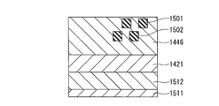
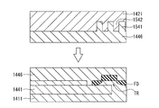
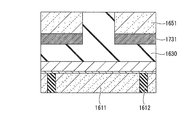
- FIG. 43A is a schematic view showing an enlarged periphery of the light attenuation portions 1501 and 1502, and FIG. 43A is a cross-sectional view showing a path of light incident on the light attenuation portions 1501 and 1502.
- FIG. 44A of the manufacturing method of the semiconductor device which concerns on 4th Embodiment of this technique. It is a process sectional view following FIG. 44B of the manufacturing method of the semiconductor device which concerns on 4th Embodiment of this technique. It is a process sectional view following FIG. 44C of the manufacturing method of the semiconductor device which concerns on 4th Embodiment of this technique. It is a process sectional view following FIG. 45D of the manufacturing method of the semiconductor device which concerns on 4th Embodiment of this technique. It is a process sectional view following FIG. 45E of the manufacturing method of the semiconductor device which concerns on 4th Embodiment of this technique. It is a process sectional view following FIG.
- FIG. 50A of the manufacturing method of the semiconductor device which concerns on modification 2 of the 4th Embodiment of this technique.
- FIG. 50B of the manufacturing method of the semiconductor device which concerns on modification 2 of the 4th Embodiment of this technique.
- FIG. 50C of the manufacturing method of the semiconductor device which concerns on modification 2 of the 4th Embodiment of this technique.
- FIG. 51D of the manufacturing method of the semiconductor device which concerns on modification 2 of the 4th Embodiment of this technique.
- FIG. 51E It is a process sectional view following FIG. 51E of the manufacturing method of the semiconductor device which concerns on modification 2 of the 4th Embodiment of this technique. It is a process sectional view following FIG. 51F of the manufacturing method of the semiconductor device which concerns on modification 2 of the 4th Embodiment of this technique. It is a process sectional view following FIG. 52G of the manufacturing method of the semiconductor device which concerns on modification 2 of the 4th Embodiment of this technique. It is a partially enlarged sectional view of the semiconductor device which concerns on the modification 3 of the 4th Embodiment of this technique. It is a process sectional view of the manufacturing method of the semiconductor device which concerns on modification 3 of 4th Embodiment of this technique. It is a process sectional view following FIG.
- FIG. 54A of the manufacturing method of the semiconductor device which concerns on modification 3 of the 4th Embodiment of this technique. It is a process sectional view following FIG. 54B of the manufacturing method of the semiconductor device which concerns on modification 3 of the 4th Embodiment of this technique. It is a process sectional view following FIG. 54C of the manufacturing method of the semiconductor device which concerns on modification 3 of the 4th Embodiment of this technique. It is a process sectional view following FIG. 55D of the manufacturing method of the semiconductor device which concerns on modification 3 of the 4th Embodiment of this technique. It is a process sectional view following FIG. 55E of the manufacturing method of the semiconductor device which concerns on modification 3 of the 4th Embodiment of this technique.
- FIG. 70 It is a partially enlarged sectional view of the semiconductor device which concerns on modification 5 of 5th Embodiment of this technique. It is a schematic block diagram of the electronic device which concerns on other embodiment of this technique. It is a block diagram which shows an example of the functional structure of the image pickup apparatus which concerns on one Embodiment of this disclosure. It is a plan schematic diagram which shows the schematic structure of the image pickup apparatus shown in FIG. 70. It is a schematic diagram which shows the cross-sectional structure along the line III-III'shown in FIG. It is an equivalent circuit diagram of the pixel sharing unit shown in FIG. 70. It is a figure which shows an example of the connection mode of a plurality of pixel sharing units and a plurality of vertical signal lines.
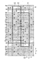
- FIG. 72 It is sectional drawing which shows an example of the specific structure of the image pickup apparatus shown in FIG. 72. It is a schematic diagram which shows an example of the plane structure of the main part of the 1st substrate shown in FIG. 75. It is a schematic diagram which shows the plane structure of the pad part together with the main part of the 1st substrate shown in FIG. 76A. It is a schematic diagram which shows an example of the plane structure of the 2nd substrate (semiconductor layer) shown in FIG. 75.
- FIG. 5 is a schematic view showing an example of a planar configuration of a pixel circuit and a main part of a first substrate together with the first wiring layer shown in FIG. 75.
- FIG. 75 It is a schematic diagram which shows an example of the plane structure of the 1st wiring layer and the 2nd wiring layer shown in FIG. 75. It is a schematic diagram which shows an example of the plane structure of the 2nd wiring layer and the 3rd wiring layer shown in FIG. 75. It is a schematic diagram which shows an example of the plane structure of the 3rd wiring layer and the 4th wiring layer shown in FIG. 75. It is a schematic diagram for demonstrating the path of the input signal to the image pickup apparatus shown in FIG. 72. It is a schematic diagram for demonstrating the signal path of the pixel signal of the image pickup apparatus shown in FIG. 72. It is a schematic diagram which shows one modification of the planar structure of the 2nd substrate (semiconductor layer) shown in FIG. 77.
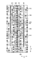
- FIG. 84 It is a schematic diagram which shows the plane structure of the main part of the 1st wiring layer and the 1st substrate together with the pixel circuit shown in FIG. 84. It is a schematic diagram which shows an example of the plane structure of the 2nd wiring layer together with the 1st wiring layer shown in FIG. 85. It is a schematic diagram which shows an example of the plane structure of the 3rd wiring layer together with the 2nd wiring layer shown in FIG. It is a schematic diagram which shows an example of the plane structure of the 4th wiring layer together with the 3rd wiring layer shown in FIG. 87. It is a schematic diagram which shows one modification of the plane structure of the 1st substrate shown in FIG. 76A. FIG.
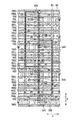
- FIG. 5 is a schematic view showing an example of a planar configuration of a second substrate (semiconductor layer) laminated on the first substrate shown in FIG. 89. It is a schematic diagram which shows an example of the plane structure of the 1st wiring layer together with the pixel circuit shown in FIG. 90. It is a schematic diagram which shows an example of the plane structure of the 2nd wiring layer together with the 1st wiring layer shown in FIG. 91. It is a schematic diagram which shows an example of the plane structure of the 3rd wiring layer together with the 2nd wiring layer shown in FIG. 92. It is a schematic diagram which shows an example of the plane structure of the 4th wiring layer together with the 3rd wiring layer shown in FIG. 93.
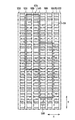
- FIG. 5 is a schematic view showing an example of a planar configuration of a second substrate (semiconductor layer) laminated on the first substrate shown in FIG. 95. It is a schematic diagram which shows an example of the plane structure of the 1st wiring layer together with the pixel circuit shown in FIG. 96. It is a schematic diagram which shows an example of the plane structure of the 2nd wiring layer together with the 1st wiring layer shown in FIG. 97. It is a schematic diagram which shows an example of the plane structure of the 3rd wiring layer together with the 2nd wiring layer shown in FIG. 98.
- FIG. 72 It is a schematic diagram which shows an example of the plane structure of the 4th wiring layer together with the 3rd wiring layer shown in FIG. It is sectional drawing which shows the other example of the image pickup apparatus shown in FIG. 72. It is a schematic diagram for demonstrating the path of the input signal to the image pickup apparatus shown in FIG. 101. It is a schematic diagram for demonstrating the signal path of the pixel signal of the image pickup apparatus shown in FIG. 101. It is sectional drawing which shows the other example of the image pickup apparatus shown in FIG. 75. It is a figure which shows another example of the equivalent circuit shown in FIG. 73.
- FIG. 6 is a schematic plan view showing another example of the pixel separation portion shown in FIG. 76A and the like.
- FIG. 113 It is a block diagram which shows an example of the schematic structure of a vehicle control system. It is explanatory drawing which shows an example of the installation position of the vehicle exterior information detection unit and the image pickup unit. It is a figure which shows an example of the schematic structure of the endoscopic surgery system. It is a block diagram which shows an example of the functional structure of a camera head and CCU.
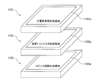
- FIG. 1 shows an example of a schematic configuration of an image pickup apparatus 1 according to a first embodiment of the present technology.
- the image pickup apparatus 1 includes three substrates (first substrate 10, second substrate 20, third substrate 30).
- the image pickup device 1 is an image pickup device having a three-dimensional structure configured by laminating three substrates (first substrate 10, second substrate 20, third substrate 30).
- the first substrate 10, the second substrate 20, and the third substrate 30 are laminated in this order.
- the first substrate 10 has a plurality of sensor pixels 12 that perform photoelectric conversion on the semiconductor substrate 11.
- the plurality of sensor pixels 12 are provided in a matrix in the pixel region 13 of the first substrate 10.
- the second substrate 20 has one readout circuit 22 for each of the four sensor pixels 12 on the semiconductor substrate 21 to output a pixel signal based on the charge output from the sensor pixel 12.
- the semiconductor substrate 21 corresponds to a specific example of the "second semiconductor substrate" of the present technology.
- the second substrate 20 has a plurality of pixel drive lines 23 extending in the row direction and a plurality of vertical signal lines 24 extending in the column direction.
- the third substrate 30 has a logic circuit 32 for processing a pixel signal on the semiconductor substrate 31.
- the semiconductor substrate 31 corresponds to a specific example of the "third semiconductor substrate" of the present technology.
- the logic circuit 32 includes, for example, a vertical drive circuit 33, a column signal processing circuit 34, a horizontal drive circuit 35, and a system control circuit 36.
- the logic circuit 32 (specifically, the horizontal drive circuit 35) outputs the output voltage Vout for each sensor pixel 12 to the outside.
- a low resistance region made of silicide formed by using a salicide (Self Aligned Silicide) process such as CoSi 2 or NiSi is formed on the surface of the impurity diffusion region in contact with the source electrode and the drain electrode. You may.
- the vertical drive circuit 33 selects a plurality of sensor pixels 12 in order in line units.
- the column signal processing circuit 34 performs, for example, Correlated Double Sampling (CDS) processing on the pixel signals output from each sensor pixel 12 in the row selected by the vertical drive circuit 33.
- CDS Correlated Double Sampling
- the column signal processing circuit 34 extracts the signal level of the pixel signal by performing CDS processing, for example, and holds pixel data corresponding to the amount of light received by each sensor pixel 12.
- the horizontal drive circuit 35 sequentially outputs the pixel data held in the column signal processing circuit 34 to the outside, for example.
- the system control circuit 36 controls, for example, the drive of each block (vertical drive circuit 33, column signal processing circuit 34, and horizontal drive circuit 35) in the logic circuit 32.
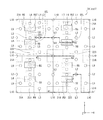
- FIG. 2 shows an example of the sensor pixel 12 and the readout circuit 22.
- FIG. 2 shows an example of the sensor pixel 12 and the readout circuit 22.
- “sharing” means that the outputs of the four sensor pixels 12 are input to the common read circuit 22.
- Each sensor pixel 12 has a component common to each other.
- an identification number (1, 2, 3, 4) is added to the end of the code of the component of each sensor pixel 12 in order to distinguish the components of each sensor pixel 12 from each other.
- an identification number is given at the end of the code of the component of each sensor pixel 12, but the components of each sensor pixel 12 are distinguished from each other. If it is not necessary to do so, the identification number at the end of the code of the component of each sensor pixel 12 shall be omitted.
- Each sensor pixel 12 is, for example, a floating diffusion that temporarily holds the electric charge output from the photodiode PD, the transfer transistor TR electrically connected to the photodiode PD, and the electric charge output from the photodiode PD via the transfer transistor TR. It has an FD.
- the photodiode PD corresponds to a specific example of the "photoelectric conversion element" of the present technology.
- the photodiode PD performs photoelectric conversion to generate an electric charge according to the amount of received light.
- the cathode of the photodiode PD is electrically connected to the source of the transfer transistor TR, and the anode of the photodiode PD is electrically connected to the reference potential line (eg, ground).
- the drain of the transfer transistor TR is electrically connected to the floating diffusion FD, and the gate of the transfer transistor TR is electrically connected to the pixel drive line 23.
- the transfer transistor TR is, for example, a CMOS (Complementary Metal Oxide Semiconductor) transistor.
- the floating diffusion FDs of the sensor pixels 12 sharing one read circuit 22 are electrically connected to each other and are also electrically connected to the input end of the common read circuit 22.
- the readout circuit 22 has, for example, a reset transistor RST, a selection transistor SEL, and an amplification transistor AMP.
- the selection transistor SEL may be omitted if necessary.
- the source of the reset transistor RST (the input end of the read circuit 22) is electrically connected to the floating diffusion FD, and the drain of the reset transistor RST is electrically connected to the power line VDD and the drain of the amplification transistor AMP.
- the gate of the reset transistor RST is electrically connected to the pixel drive line 23 (see FIG. 1).
- the source of the amplification transistor AMP is electrically connected to the drain of the selection transistor SEL, and the gate of the amplification transistor AMP is electrically connected to the source of the reset transistor RST.
- the source of the selection transistor SEL (the output end of the readout circuit 22) is electrically connected to the vertical signal line 24, and the gate of the selection transistor SEL is electrically connected to the pixel drive line 23 (see FIG. 1). ..
- the transfer transistor TR When the transfer transistor TR is turned on, the transfer transistor TR transfers the electric charge of the photodiode PD to the floating diffusion FD.
- the gate of the transfer transistor TR extends from the surface of the semiconductor substrate 11 to a depth that penetrates the well layer 42 and reaches PD41, for example, as shown in FIG. 4 described later.
- the reset transistor RST resets the potential of the floating diffusion FD to a predetermined potential.
- the reset transistor RST is turned on, the potential of the floating diffusion FD is reset to the potential of the power supply line VDD.
- the selection transistor SEL controls the output timing of the pixel signal from the readout circuit 22.
- the amplification transistor AMP generates a signal of a voltage corresponding to the level of the electric charge held in the floating diffusion FD as a pixel signal.
- the amplification transistor AMP constitutes a source follower type amplifier, and outputs a pixel signal having a voltage corresponding to the level of electric charge generated by the photodiode PD.
- the selection transistor SEL When the selection transistor SEL is turned on, the amplification transistor AMP amplifies the potential of the floating diffusion FD and outputs a voltage corresponding to the potential to the column signal processing circuit 34 via the vertical signal line 24.
- the reset transistor RST, amplification transistor AMP and selection transistor SEL are, for example, CMOS transistors.
- the source of the amplification transistor AMP (the output end of the readout circuit 22) is electrically connected to the vertical signal line 24, and the FD transfer transistor FDG is provided between the source of the reset transistor RST and the gate of the amplification transistor AMP.
- the gate of the amplification transistor AMP is electrically connected to the source of the FD transfer transistor FDG.
- the FD transfer transistor FDG is used when switching the conversion efficiency.
- the FD transfer transistor FDG when the FD transfer transistor FDG is turned on, the gate capacitance for the FD transfer transistor FDG increases, so that the overall FD capacitance C increases. On the other hand, when the FD transfer transistor FDG is turned off, the overall FD capacitance C becomes smaller. By switching the FD transfer transistor FDG on and off in this way, the FD capacitance C can be made variable and the conversion efficiency can be switched.
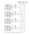
- FIG. 3 shows an example of a connection mode between the plurality of readout circuits 22 and the plurality of vertical signal lines 24.
- the plurality of read circuits 22 are arranged side by side in the extending direction (for example, the column direction) of the vertical signal lines 24, even if one of the plurality of vertical signal lines 24 is assigned to each read circuit 22. Good.
- the four vertical signal lines 24 are the read circuits 22. It may be assigned one for each.
- an identification number (1, 2, 3, 4) is added to the end of the code of each vertical signal line 24.
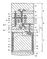
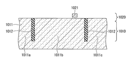
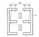
- FIG. 4 shows an example of the cross-sectional configuration of the image pickup apparatus 1 in the vertical direction.
- FIG. 4 illustrates a cross-sectional configuration of a portion of the image pickup apparatus 1 facing the sensor pixel 12.
- the image pickup apparatus 1 is configured by laminating the first substrate 10, the second substrate 20, and the third substrate 30 in this order, and further, the color filter 40 is on the back surface side (light incident surface side) of the first substrate 10. And a light receiving lens 50.
- One color filter 40 and one light receiving lens 50 are provided for each sensor pixel 12, for example. That is, the image pickup device 1 is a back-illuminated image pickup device.
- the first substrate 10 is configured by laminating an insulating layer 46 on a semiconductor substrate 11.
- the insulating layer 46 corresponds to a specific example of the "first insulating layer" of the present technology.
- the first substrate 10 has an insulating layer 46 as a part of the interlayer insulating film 51.
- the insulating layer 46 is provided in the gap between the semiconductor substrate 11 and the semiconductor substrate 21 described later.
- the semiconductor substrate 11 is made of a silicon substrate.
- the semiconductor substrate 11 has, for example, a p-well layer 42 in a part of the surface or in the vicinity thereof, and in other regions (a region deeper than the p-well layer 42), the conductivity is different from that of the p-well layer 42. It has a type PD41.
- the p-well layer 42 is composed of a p-type semiconductor region.
- the PD 41 is composed of a conductive type (specifically, n type) semiconductor region different from the p-well layer 42.
- the semiconductor substrate 11 has a floating diffusion FD in the p-well layer 42 as a conductive type (specifically, n-type) semiconductor region different from the p-well layer 42.
- the first substrate 10 has a photodiode PD, a transfer transistor TR, and a floating diffusion FD for each sensor pixel 12.
- the first substrate 10 has a configuration in which a transfer transistor TR and a floating diffusion FD are provided on a portion of the semiconductor substrate 11 on the surface side (the side opposite to the light incident surface side, the second substrate 20 side).
- the first substrate 10 has an element separation unit 43 that separates each sensor pixel 12.
- the element separation portion 43 is formed so as to extend in the normal direction of the semiconductor substrate 11 (the direction perpendicular to the surface of the semiconductor substrate 11).
- the element separation unit 43 is provided between two sensor pixels 12 adjacent to each other.
- the element separation unit 43 electrically separates the sensor pixels 12 adjacent to each other.
- the element separation unit 43 is made of, for example, silicon oxide.
- the element separation unit 43 penetrates, for example, the semiconductor substrate 11.
- the first substrate 10 further has, for example, a p-well layer 44 which is a side surface of the element separating portion 43 and is in contact with the surface on the photodiode PD side.
- the p-well layer 44 is composed of a conductive type (specifically, p-type) semiconductor region different from the photodiode PD.
- the first substrate 10 further has, for example, a fixed charge film 45 in contact with the back surface of the semiconductor substrate 11.
- the fixed charge film 45 is negatively charged in order to suppress the generation of dark current due to the interface state on the light receiving surface side of the semiconductor substrate 11.
- the fixed charge film 45 is formed of, for example, an insulating film having a negative fixed charge.
- the material of such an insulating film examples include hafnium oxide, zircon oxide, aluminum oxide, titanium oxide and tantalum oxide.
- the electric field induced by the fixed charge film 45 forms a hole storage layer at the interface on the light receiving surface side of the semiconductor substrate 11.
- the hole accumulation layer suppresses the generation of electrons from the interface.
- the color filter 40 is provided on the back surface side of the semiconductor substrate 11.
- the color filter 40 is provided, for example, in contact with the fixed charge film 45, and is provided at a position facing the sensor pixel 12 via the fixed charge film 45.
- the light receiving lens 50 is provided, for example, in contact with the color filter 40, and is provided at a position facing the sensor pixel 12 via the color filter 40 and the fixed charge film 45.
- the second substrate 20 is configured by laminating an insulating layer 52 on a semiconductor substrate 21.
- the insulating layer 52 corresponds to a specific example of the "third insulating layer" of the present technology.
- the second substrate 20 has an insulating layer 52 as a part of the interlayer insulating film 51.
- the insulating layer 52 is provided in the gap between the semiconductor substrate 21 and the semiconductor substrate 31.
- the semiconductor substrate 21 is made of a silicon substrate.
- the second substrate 20 has one readout circuit 22 for every four sensor pixels 12.
- the second substrate 20 has a configuration in which a readout circuit 22 is provided on a portion on the surface side (third substrate 30 side) of the semiconductor substrate 21.
- the second substrate 20 is attached to the first substrate 10 with the back surface of the semiconductor substrate 21 facing the front surface side of the semiconductor substrate 11. That is, the second substrate 20 is attached to the first substrate 10 face-to-back.
- the second substrate 20 further has an insulating layer 53 penetrating the semiconductor substrate 21 in the same layer as the semiconductor substrate 21.
- the insulating layer 53 corresponds to a specific example of the "second insulating layer" of the present technology.
- the second substrate 20 has an insulating layer 53 as a part of the interlayer insulating film 51.
- the insulating layer 53 is provided so as to cover the side surface of the through wiring 54 described later.
- the laminate composed of the first substrate 10 and the second substrate 20 has an interlayer insulating film 51 and a through wiring 54 provided in the interlayer insulating film 51.
- the through wiring 54 corresponds to a specific example of the "first through wiring" of the present technology.
- the laminated body has one through wiring 54 for each sensor pixel 12.
- the through wiring 54 extends in the normal direction of the semiconductor substrate 21, and is provided so as to penetrate the portion of the interlayer insulating film 51 including the insulating layer 53.
- the first substrate 10 and the second substrate 20 are electrically connected to each other by a through wiring 54.
- the through wiring 54 is electrically connected to the floating diffusion FD and the connection wiring 55 described later.
- the laminate composed of the first substrate 10 and the second substrate 20 further has through wirings 47 and 48 (see FIG. 10 described later) provided in the interlayer insulating film 51.
- the through wiring 48 corresponds to a specific example of the "first through wiring" of the present technology.
- the laminated body has one through wiring 47 and one through wiring 48 for each sensor pixel 12.
- the through wirings 47 and 48 extend in the normal direction of the semiconductor substrate 21, respectively, and are provided so as to penetrate the portion of the interlayer insulating film 51 including the insulating layer 53.
- the first substrate 10 and the second substrate 20 are electrically connected to each other by through wirings 47 and 48.
- the through wiring 47 is electrically connected to the p-well layer 42 of the semiconductor substrate 11 and the wiring in the second substrate 20.
- the through wiring 48 is electrically connected to the transfer gate TG and the pixel drive line 23.
- the second substrate 20 has, for example, a plurality of connecting portions 59 electrically connected to the readout circuit 22 and the semiconductor substrate 21 in the insulating layer 52.
- the second substrate 20 further has, for example, a wiring layer 56 on the insulating layer 52.
- the wiring layer 56 has, for example, an insulating layer 57, a plurality of pixel drive lines 23 provided in the insulating layer 57, and a plurality of vertical signal lines 24.
- the wiring layer 56 further has, for example, a plurality of connection wirings 55 in the insulating layer 57, one for each of the four sensor pixels 12.
- the connection wiring 55 electrically connects each through wiring 54 electrically connected to the floating diffusion FD included in the four sensor pixels 12 sharing the read circuit 22 to each other.
- the total number of the through wirings 54 and 48 is larger than the total number of the sensor pixels 12 included in the first substrate 10, and is twice the total number of the sensor pixels 12 included in the first substrate 10. Further, the total number of the through wirings 54, 48, 47 is larger than the total number of the sensor pixels 12 included in the first substrate 10, and is three times the total number of the sensor pixels 12 included in the first substrate 10.
- the wiring layer 56 further has, for example, a plurality of pad electrodes 58 in the insulating layer 57.
- Each pad electrode 58 is made of, for example, a metal such as Cu (copper) or Al (aluminum).
- Each pad electrode 58 is exposed on the surface of the wiring layer 56.
- Each pad electrode 58 is used for electrical connection between the second substrate 20 and the third substrate 30 and for bonding the second substrate 20 and the third substrate 30.
- the plurality of pad electrodes 58 are provided, for example, one for each of the pixel drive line 23 and the vertical signal line 24.
- the total number of pad electrodes 58 (or the total number of joints between the pad electrodes 58 and the pad electrodes 64 (described later)) is smaller than the total number of sensor pixels 12 included in the first substrate 10.
- the third substrate 30 is configured by, for example, laminating an interlayer insulating film 61 on a semiconductor substrate 31. As will be described later, the third substrate 30 is attached to the second substrate 20 with the surfaces on the front side facing each other. Therefore, when explaining the configuration inside the third substrate 30, the upper and lower parts will be described. , It is the opposite of the vertical direction in the drawing.
- the semiconductor substrate 31 is made of a silicon substrate.
- the third substrate 30 has a configuration in which a logic circuit 32 is provided on a portion on the surface side of the semiconductor substrate 31.
- the third substrate 30 further has, for example, a wiring layer 62 on the interlayer insulating film 61.
- the wiring layer 62 has, for example, an insulating layer 63 and a plurality of pad electrodes 64 provided in the insulating layer 63.
- the plurality of pad electrodes 64 are electrically connected to the logic circuit 32.
- Each pad electrode 64 is made of, for example, Cu (copper).
- Each pad electrode 64 is exposed on the surface of the wiring layer 62.
- Each pad electrode 64 is used for electrical connection between the second substrate 20 and the third substrate 30 and for bonding the second substrate 20 and the third substrate 30. Further, the number of pad electrodes 64 does not necessarily have to be plurality, and even one pad electrode 64 can be electrically connected to the logic circuit 32.
- the second substrate 20 and the third substrate 30 are electrically connected to each other by joining the pad electrodes 58 and 64 to each other.
- the gate of the transfer transistor TR (transfer gate TG) is electrically connected to the logic circuit 32 via the through wiring 54 and the pad electrodes 58 and 64.
- the third substrate 30 is attached to the second substrate 20 with the surface of the semiconductor substrate 31 facing the surface side of the semiconductor substrate 21. That is, the third substrate 30 is attached to the second substrate 20 face-to-face.
- the chip size may increase or the area per pixel may be reduced due to the structure in which the semiconductor substrates are electrically connected to each other. There is sex.
- the sensor pixels 12 and the readout circuit 22 are formed on different substrates (first substrate 10 and second substrate 20).
- the area of the sensor pixel 12 and the readout circuit 22 can be expanded as compared with the case where the sensor pixel 12 and the readout circuit 22 are formed on the same substrate.
- the photoelectric conversion efficiency can be improved and the transistor noise can be reduced.
- the first substrate 10 having the sensor pixels 12 and the second substrate 20 having the readout circuit 22 are electrically connected to each other by a through wiring 54 provided in the interlayer insulating film 51.
- the chip size can be made smaller. Further, the resolution can be further increased by further miniaturizing the area per pixel. Further, when the chip size is the same as before, the formation region of the sensor pixel 12 can be expanded. Further, in the present embodiment, the read circuit 22 and the logic circuit 32 are formed on different substrates (second substrate 20 and third substrate 30). As a result, the areas of the read circuit 22 and the logic circuit 32 can be expanded as compared with the case where the read circuit 22 and the logic circuit 32 are formed on the same substrate.
- the second substrate 20 and the third substrate 30 are electrically connected to each other by joining the pad electrodes 58 and 64 to each other.
- the read circuit 22 is formed on the second substrate 20 and the logic circuit 32 is formed on the third substrate 30, the second substrate 20 and the third substrate 30 can be electrically connected to each other.
- the structure for electrically connecting the first substrate 10 and the second substrate 20 to each other it is possible to form the structure in a more flexible layout such as the number of contacts for arrangement and connection. ..
- the bonding of the pad electrodes 58 and 64 can be used for the electrical connection between the second substrate 20 and the third substrate 30.
- the substrates are electrically connected to each other according to the degree of integration of the substrates.
- the chip size does not increase or the miniaturization of the area per pixel is not hindered due to the structure in which the substrates are electrically connected to each other.
- the sensor pixel 12 having the photodiode PD, the transfer transistor TR and the floating diffusion FD is formed on the first substrate 10, and the read circuit 22 having the reset transistor RST, the amplification transistor AMP and the selection transistor SEL is formed. It is formed on the second substrate 20.
- the area of the sensor pixel 12 and the readout circuit 22 can be expanded as compared with the case where the sensor pixel 12 and the readout circuit 22 are formed on the same substrate.
- the pad electrodes 58 and 64 are joined to each other for the electrical connection between the second substrate 20 and the third substrate 30, the chip size becomes large and the area per pixel increases. It does not hinder miniaturization.
- the area of the photodiode PD of the sensor pixel 12 can be expanded by reducing the number of transistors provided on the first substrate 10. As a result, the amount of saturated signal charge in photoelectric conversion can be increased, and the photoelectric conversion efficiency can be improved.
- the degree of freedom in the layout of each transistor in the readout circuit 22 can be ensured. Further, since the area of each transistor can be expanded, noise affecting the pixel signal can be reduced by particularly expanding the area of the amplification transistor AMP.
- the chip size can be increased and the area per pixel can be reduced. It does not interfere. As a result, it is possible to provide an image pickup device 1 having a three-layer structure that has the same chip size as before and does not hinder the miniaturization of the area per pixel.
- the second substrate 20 is attached to the first substrate 10 with the back surface of the semiconductor substrate 21 facing the front surface side of the semiconductor substrate 11, and the third substrate 30 is the surface of the semiconductor substrate 21. It is attached to the second substrate 20 with the front surface side of the semiconductor substrate 31 facing side.
- the through wiring 54 is used for the electrical connection between the first substrate 10 and the second substrate 20, and the pad electrodes 58 and 64 are joined to each other for the electrical connection between the second substrate 20 and the third substrate 30.
- the cross-sectional area of the through wiring 54 is smaller than the cross-sectional area of the joint portion between the pad electrodes 58 and 64.
- the region is formed.
- the low resistance region made of silicide is formed of a compound of the material of the semiconductor substrate and the metal.
- the logic circuit 32 is provided on the third substrate 30. Therefore, the logic circuit 32 can be formed by a process different from the process of forming the sensor pixel 12 and the read circuit 22. As a result, a high temperature process such as thermal oxidation can be used when forming the sensor pixel 12 and the readout circuit 22.
- VDD which is a material having low heat resistance
- the contact resistance can be reduced, and as a result, the logic circuit 32 can be used.
- the calculation speed can be increased.
- the first substrate 10 is provided with an element separation unit 43 for separating each sensor pixel 12.
- the sensor pixel 12 having the photodiode PD, the transfer transistor TR and the floating diffusion FD is formed on the first substrate 10, and the read circuit 22 having the reset transistor RST, the amplification transistor AMP and the selection transistor SEL is formed. It is formed on the second substrate 20.
- the area of the sensor pixel 12 and the readout circuit 22 can be expanded even when the area surrounded by the element separation unit 43 is reduced due to the miniaturization of the area per pixel.
- the chip size does not increase and the miniaturization of the area per pixel is not hindered. Therefore, it is possible to provide an image pickup device 1 having a three-layer structure that does not hinder the miniaturization of the area per pixel with the same chip size as before.
- the element separation unit 43 penetrates the semiconductor substrate 11. As a result, even when the distance between the sensor pixels 12 becomes closer due to the miniaturization of the area per pixel, signal crosstalk between the adjacent sensor pixels 12 can be suppressed, and the resolution on the reproduced image is lowered. Image quality deterioration due to color mixing can be suppressed.
- the laminate composed of the first substrate 10 and the second substrate 20 has three through wirings 54, 47, 48 for each sensor pixel 12.
- the through wiring 54 is electrically connected to the gate (transfer gate TG) of the transfer transistor TR, the through wiring 47 is electrically connected to the p-well layer 42 of the semiconductor substrate 11, and the through wiring 48 is a floating diffusion FD. Is electrically connected to. That is, the number of through wires 54, 47, and 48 is larger than the number of sensor pixels 12 included in the first substrate 10.
- the through wiring 54 having a small cross-sectional area is used for the electrical connection between the first substrate 10 and the second substrate 20.
- the chip size can be further reduced, and the area per pixel on the first substrate 10 can be further reduced.
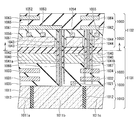
- FIG. 5 shows an example of a modification of the vertical cross-sectional configuration of the image pickup apparatus 1 according to the above embodiment.
- FIG. 5 shows a modified example of the cross-sectional configuration shown in FIG.
- the transfer transistor TR has a planar transfer gate TG. Therefore, the transfer gate TG does not penetrate the well layer 42 and is formed only on the surface of the semiconductor substrate 11. Even when a planar transfer gate TG is used for the transfer transistor TR, the image pickup apparatus 1 has the same effect as that of the above embodiment.
- [Modification B] 6 and 7 show a modification of the horizontal cross-sectional configuration of the image pickup apparatus 1 according to the above embodiment.
- the upper view of FIGS. 6 and 7 is a modification of the cross-sectional configuration of the cross section Sec1 of FIG. 4, and the lower view of FIG. 6 is a modification of the cross-sectional configuration of the cross section Sec2 of FIG. is there.
- a diagram showing a modified example of the surface configuration of the semiconductor substrate 11 of FIG. 4 is superimposed on a diagram showing a modified example of the cross-sectional configuration of the cross section Sec1 of FIG.
- the insulating layer 46 is omitted.
- a diagram showing a modified example of the surface configuration of the semiconductor substrate 21 is superimposed on a diagram showing a modified example of the cross-sectional configuration in the cross-sectional section Sec2 of FIG. There is.
- the plurality of through wires 54, the plurality of through wires 48, and the plurality of through wires 47 are the surfaces of the first substrate 10. Inside, they are arranged side by side in a band shape in the first direction V1 (left and right directions in FIGS. 6 and 7). Note that FIGS. 6 and 7 illustrate a case where a plurality of through wires 54, a plurality of through wires 48, and a plurality of through wires 47 are arranged side by side in two rows in the first direction V1. In the four sensor pixels 12 sharing the readout circuit 22, the four floating diffusion FDs are arranged close to each other, for example, via the element separation unit 43.
- the four transfer gates TGs (TG1, TG2, TG3, TG4) are arranged so as to surround the four floating diffusion FDs, for example, the four transfer gates TGs. It has a ring shape.
- the insulating layer 53 is composed of a plurality of blocks extending in the first direction V1.
- the semiconductor substrate 21 is composed of a plurality of island-shaped blocks 21A extending in the first direction V1 and arranged side by side in the second direction V2 orthogonal to the first direction V1 via an insulating layer 53. ..
- Each block 21A is provided with, for example, a reset transistor RST, an amplification transistor AMP, and a selection transistor SEL.
- One read-out circuit 22 shared by the four sensor pixels 12 is not arranged facing the four sensor pixels 12, for example, but is arranged so as to be offset in the second direction V2.
- one read-out circuit 22 shared by the four sensor pixels 12 is a reset transistor in the second substrate 20 in which the region facing the four sensor pixels 12 is shifted in the second direction V2. It is composed of RST, amplification transistor AMP and selection transistor SEL.
- One read-out circuit 22 shared by the four sensor pixels 12 is composed of, for example, an amplification transistor AMP, a reset transistor RST, and a selection transistor SEL in one block 21A.
- one read-out circuit 22 shared by the four sensor pixels 12 is a reset transistor in the second substrate 20 in which the region facing the four sensor pixels 12 is shifted in the second direction V2. It is composed of RST, amplification transistor AMP, selection transistor SEL and FD transfer transistor FDG.
- One read-out circuit 22 shared by the four sensor pixels 12 is composed of, for example, an amplification transistor AMP, a reset transistor RST, a selection transistor SEL, and an FD transfer transistor FDG in one block 21A.
- one readout circuit 22 shared by the four sensor pixels 12 is not arranged to face the four sensor pixels 12, for example, and is second from a position facing the four sensor pixels 12. It is arranged so as to be offset in the direction V2.
- the wiring 25 can be shortened, or the wiring 25 can be omitted and the source of the amplification transistor AMP and the drain of the selection transistor SEL can be configured in a common impurity region. ..
- the size of the read circuit 22 can be reduced, and the size of other parts of the read circuit 22 can be increased.
- FIG. 8 shows an example of a modification of the horizontal cross-sectional configuration of the image pickup apparatus 1 according to the above embodiment.
- FIG. 8 shows a modified example of the cross-sectional configuration of FIG.
- the semiconductor substrate 21 is composed of a plurality of island-shaped blocks 21A arranged side by side in the first direction V1 and the second direction V2 via the insulating layer 53.
- Each block 21A is provided with, for example, a set of reset transistor RST, amplification transistor AMP, and selection transistor SEL.
- the crosstalk between the readout circuits 22 adjacent to each other can be suppressed by the insulating layer 53, and the resolution deterioration on the reproduced image and the image quality deterioration due to color mixing can be suppressed.
- FIG. 9 shows an example of a cross-sectional configuration in the horizontal direction of the image pickup apparatus 1 according to the above embodiment and a modified example thereof.
- the first substrate 10 has a photodiode PD and a transfer transistor TR for each sensor pixel 12, and a floating diffusion FD is shared for each of the four sensor pixels 12. Therefore, in this modification, one through wiring 54 is provided for each of the four sensor pixels 12.
- the first substrate 10 shares the through wiring 47 for each of the four sensor pixels 12A. Therefore, in this modified example, one through wiring 47 is provided for every four sensor pixels 12A.
- the first substrate 10 has an element separation unit 43 that separates the photodiode PD and the transfer transistor TR for each sensor pixel 12.
- the element separation unit 43 does not completely surround the sensor pixel 12 when viewed from the normal direction of the semiconductor substrate 11, and has a gap (through wiring 54) and a gap (through wiring 47) in the vicinity of the floating diffusion FD (through wiring 54). It has an unformed region). The gap allows the four sensor pixels 12 to share one through wiring 54 and the four sensor pixels 12A to share one through wiring 47.
- the second substrate 20 has a readout circuit 22 for each of the four sensor pixels 12 that share the floating diffusion FD.
- FIG. 10 shows an example of the circuit configuration of the image pickup apparatus 1 according to the above-described embodiment and its modified example.
- the image pickup apparatus 1 according to this modification is a CMOS image sensor equipped with a row-parallel ADC.
- the image pickup apparatus 1 is vertically driven in addition to the pixel region 13 in which a plurality of sensor pixels 12 including a photoelectric conversion element are two-dimensionally arranged in a matrix shape.
- the configuration includes a circuit 33, a column signal processing circuit 34, a reference voltage supply unit 38, a horizontal drive circuit 35, a horizontal output line 37, and a system control circuit 36.
- the system control circuit 36 is based on the master clock MCK, and is a clock signal or control that serves as a reference for the operation of the vertical drive circuit 33, the column signal processing circuit 34, the reference voltage supply unit 38, the horizontal drive circuit 35, and the like.
- a signal or the like is generated and given to the vertical drive circuit 33, the column signal processing circuit 34, the reference voltage supply unit 38, the horizontal drive circuit 35, and the like.
- the vertical drive circuit 33 is formed on the first substrate 10 together with each sensor pixel 12 in the pixel region 13, and is further formed on the second substrate 20 on which the readout circuit 22 is formed.
- the column signal processing circuit 34, the reference voltage supply unit 38, the horizontal drive circuit 35, the horizontal output line 37, and the system control circuit 36 are formed on the third substrate 30.
- the sensor pixel 12 has a configuration including, for example, a transfer transistor TR that transfers the electric charge obtained by photoelectric conversion by the photodiode PD to the floating diffusion FD in addition to the photodiode PD. Can be used.
- the readout circuit 22 includes, for example, a reset transistor RST that controls the potential of the floating diffusion FD, an amplification transistor AMP that outputs a signal corresponding to the potential of the floating diffusion FD, and pixel selection.
- a three-transistor configuration having a selection transistor SEL for performing the above can be used.
- the sensor pixels 12 are two-dimensionally arranged, and the pixel drive lines 23 are wired for each row and the vertical signal lines 24 are wired for each column with respect to the pixel arrangement of m rows and n columns. There is.
- Each end of each of the plurality of pixel drive lines 23 is connected to each output end corresponding to each line of the vertical drive circuit 33.
- the vertical drive circuit 33 is configured by a shift register or the like, and controls the row address and row scan of the pixel region 13 via a plurality of pixel drive lines 23.
- the column signal processing circuit 34 has, for example, ADCs (analog-to-digital conversion circuits) 34-1 to 34-m provided for each pixel row in the pixel region 13, that is, for each vertical signal line 24, and has The analog signal output from each sensor pixel 12 for each column is converted into a digital signal and output.
- ADCs analog-to-digital conversion circuits
- the reference voltage supply unit 38 has, for example, a DAC (digital-to-analog conversion circuit) 38A as a means for generating a reference voltage Vref of a so-called ramp (RAMP) waveform whose level changes in an inclined manner over time.
- DAC digital-to-analog conversion circuit
- the means for generating the reference voltage Vref of the lamp waveform is not limited to the DAC38A.
- the DAC38A Under the control of the control signal CS1 given by the system control circuit 36, the DAC38A generates a reference voltage Vref of the lamp waveform based on the clock CK given by the system control circuit 36, and ADC34-1 of the column processing unit 15. Supply for ⁇ 34-m.
- the exposure time of the sensor pixel 12 is 1 / N as compared with the normal frame rate mode in the progressive scanning method for reading the information of all the sensor pixels 12 and the normal frame rate mode.
- the AD conversion operation corresponding to each operation mode such as a high-speed frame rate mode in which the frame rate is set to N times, for example, twice, can be selectively performed.
- This operation mode switching is executed by control by the control signals CS2 and CS3 given from the system control circuit 36. Further, the system control circuit 36 is given instruction information for switching between the normal frame rate mode and the high-speed frame rate mode from an external system controller (not shown).
- the ADC 34-m is configured to include a comparator 34A, a counting means such as an up / down counter (denoted as U / DNT in the figure) 34B, a transfer switch 34C, and a memory device 34D.
- a comparator 34A a counting means such as an up / down counter (denoted as U / DNT in the figure) 34B, a transfer switch 34C, and a memory device 34D.
- the comparator 34A has a signal voltage Vx of the vertical signal line 24 corresponding to the signal output from each sensor pixel 12 in the nth column of the pixel area 13 and a reference voltage Vref of the lamp waveform supplied from the reference voltage supply unit 38.
- Vref the reference voltage
- the output Vco becomes the "H" level
- the reference voltage Vref is equal to or less than the signal voltage Vx
- the output Vco becomes the "L" level. ..
- the up / down counter 34B is an asynchronous counter, and a clock CK is given from the system control circuit 36 at the same time as the DAC18A under the control by the control signal CS2 given from the system control circuit 36, and is down in synchronization with the clock CK ( By performing a DOWN) count or an UP count, the comparison period from the start of the comparison operation to the end of the comparison operation on the comparator 34A is measured.
- the comparison time at the time of the first reading is measured by performing a down count at the time of the first reading operation, and the second time.
- the comparison time at the time of the second reading is measured by performing an upcount at the time of the reading operation of.
- the count result for the sensor pixel 12 in one row is held as it is, and the sensor pixel 12 in the next row is continuously down-counted at the first read operation from the previous count result.
- the comparison time at the time of the first reading is measured, and by performing the upcount at the time of the second reading operation, the comparison time at the time of the second reading is measured.
- the transfer switch 34C is turned on (in the normal frame rate mode) when the counting operation of the up / down counter 34B for the sensor pixel 12 in a certain row is completed under the control by the control signal CS3 given from the system control circuit 36. In the closed state, the count result of the up / down counter 34B is transferred to the memory device 34D.
- the sensor in the next row remains in the off (open) state when the counting operation of the up / down counter 34B for the sensor pixel 12 in one row is completed.
- the state is turned on and the counting result for the two vertical pixels of the up / down counter 34B is transferred to the memory device 34D.
- the analog signals supplied from each sensor pixel 12 in the pixel region 13 via the vertical signal line 24 for each row are generated by the comparator 34A and the up / down counter 34B in the ADCs 34-1 to 34-m. By each operation, it is converted into an N-bit digital signal and stored in the memory device 34D.
- the horizontal drive circuit 35 is composed of a shift register and the like, and controls the column addresses and column scans of ADCs 34-1 to 34-m in the column signal processing circuit 34. Under the control of the horizontal drive circuit 35, the N-bit digital signals AD-converted by each of the ADCs 34-1 to 34-m are sequentially read out to the horizontal output line 37 and passed through the horizontal output line 37. It is output as imaging data.
- the count result of the up / down counter 34B can be selectively transferred to the memory device 34D via the transfer switch 34C, so that the up / down counter 34B can be up / down. It is possible to independently control the counting operation of the down counter 34B and the reading operation of the counting result of the up / down counter 34B to the horizontal output line 37.
- FIG. 11 shows an example in which the image pickup apparatus of FIG. 10 is configured by laminating three substrates (first substrate 10, second substrate 20, third substrate 30).
- first substrate 10 a pixel region 13 including a plurality of sensor pixels 12 is formed in the central portion, and a vertical drive circuit 33 is formed around the pixel region 13.
- second substrate 20 a read circuit region 15 including a plurality of read circuits 22 is formed in the central portion, and a vertical drive circuit 33 is formed around the read circuit region 15.
- a column signal processing circuit 34, a horizontal drive circuit 35, a system control circuit 36, a horizontal output line 37, and a reference voltage supply unit 38 are formed on the third substrate 30.
- the vertical drive circuit 33 may be formed only on the first substrate 10 or only on the second substrate 20.
- FIG. 12 shows a modified example of the cross-sectional configuration of the image pickup apparatus 1 according to the above-described embodiment and its modified example.
- the image pickup apparatus 1 is configured by laminating three substrates (first substrate 10, second substrate 20, third substrate 30).
- the image pickup apparatus 1 may be configured by laminating two substrates (first substrate 10, second substrate 20).
- the logic circuit 32 is formed separately from the first substrate 10 and the second substrate 20.
- a high dielectric constant film made of a material (for example, high-k) capable of withstanding a high temperature process and a metal gate electrode are laminated.
- a transistor having a gate structure is provided.
- the circuit 32B provided on the second substrate 20 side from the silicide formed on the surface of the impurity diffusion region in contact with the source electrode and the drain electrode by using a salicide (Self Aligned Silicide) process such as CoSi 2 or NiSi.
- a low resistance region 26 is formed.
- the low resistance region made of silicide is formed of a compound of the material of the semiconductor substrate and the metal.
- a high temperature process such as thermal oxidation can be used when forming the sensor pixel 12.
- a low resistance region 26 made of silicide is provided on the surface of the impurity diffusion region in contact with the source electrode and the drain electrode, contact is made. The resistance can be reduced. As a result, the calculation speed in the logic circuit 32 can be increased.
- FIG. 13 shows a modified example of the cross-sectional configuration of the image pickup apparatus 1 according to the above-described embodiment and its modified example.
- a salicide (Self Aligned Silicide) process such as CoSi 2 or NiSi is used on the surface of the impurity diffusion region in contact with the source electrode and the drain electrode.
- a low resistance region 37 made of the formed silicide may be formed.
- a high temperature process such as thermal oxidation can be used when forming the sensor pixel 12.
- the contact resistance can be reduced. As a result, the calculation speed in the logic circuit 32 can be increased.
- the conductive type may be reversed.
- the p-type may be read as the n-type and the n-type may be read as the p-type. Even in this case, the same effect as that of the above-described embodiment and its modification can be obtained.
- FIG. 14 shows an example of a schematic configuration of an imaging system 2 including an imaging device 1 according to the above embodiment and a modified example thereof.
- the imaging system 2 is, for example, an imaging device such as a digital still camera or a video camera, or an electronic device such as a mobile terminal device such as a smartphone or a tablet terminal.
- the image pickup system 2 includes, for example, an image pickup device 1, a DSP circuit 141, a frame memory 142, a display unit 143, a storage unit 144, an operation unit 145, and a power supply unit 146 according to the above embodiment and its modification.
- the image pickup device 1, the DSP circuit 141, the frame memory 142, the display unit 143, the storage unit 144, the operation unit 145, and the power supply unit 146 according to the above-described embodiment and its modification are via the bus line 147. They are interconnected.
- the image pickup apparatus 1 outputs image data according to the incident light.
- the DSP circuit 141 is a signal processing circuit that processes a signal (image data) output from the image pickup apparatus 1 according to the above embodiment and its modification.
- the frame memory 142 temporarily holds the image data processed by the DSP circuit 141 in frame units.
- the display unit 143 comprises a panel-type display device such as a liquid crystal panel or an organic EL (ElectroLuminescence) panel, and displays a moving image or a still image captured by the image pickup device 1 according to the above embodiment and its modified example. ..
- the storage unit 144 records image data of a moving image or a still image captured by the imaging device 1 according to the above embodiment and its modified example on a recording medium such as a semiconductor memory or a hard disk.
- the operation unit 145 issues operation commands for various functions of the image pickup system 2 according to the operation by the user.
- the power supply unit 146 supplies various power sources that serve as operating power sources for the image pickup device 1, the DSP circuit 141, the frame memory 142, the display unit 143, the storage unit 144, and the operation unit 145 according to the above embodiment and its modification. Supply to the subject as appropriate.
- FIG. 15 shows an example of a flowchart of an imaging operation in the imaging system 2.
- the user instructs the start of imaging by operating the operation unit 145 (step S101).
- the operation unit 145 transmits an imaging command to the imaging device 1 (step S102).
- the imaging device 1 Upon receiving an imaging command, the imaging device 1 (specifically, the system control circuit 36) executes imaging by a predetermined imaging method (step S103).
- the image pickup device 1 outputs the image data obtained by the image pickup to the DSP circuit 141.
- the image data is data for all pixels of the pixel signal generated based on the electric charge temporarily held in the floating diffusion FD.
- the DSP circuit 141 performs predetermined signal processing (for example, noise reduction processing) based on the image data input from the image pickup apparatus 1 (step S104).
- the DSP circuit 141 stores the image data subjected to the predetermined signal processing in the frame memory 142, and the frame memory 142 stores the image data in the storage unit 144 (step S105). In this way, the imaging in the imaging system 2 is performed.
- the image pickup apparatus 1 according to the above embodiment and its modification is applied to the image pickup system 2.
- the image pickup device 1 can be miniaturized or high-definition, so that a small-sized or high-definition image pickup system 2 can be provided.
- the semiconductor device according to the first embodiment of the present technology includes a pixel region (unit cell region) 1001, a vertical drive circuit 1003, a column signal processing circuit 1004, a horizontal drive circuit 1005, an output circuit 1006, and a control.
- the circuit 1007 is provided.
- the pixel region 1001 has a plurality of pixels (unit cells) 1002 arranged in a two-dimensional matrix.
- Each of the plurality of pixels 1002 has a photoelectric conversion unit and a plurality of pixel transistors (cell circuits).
- the plurality of pixel transistors for example, four transistors such as a transfer transistor, a reset transistor, a selection transistor, and an amplification transistor can be adopted.
- the vertical drive circuit 1003 is composed of, for example, a shift register.
- the vertical drive circuit 1003 sequentially selects the pixel drive wiring 1008a, supplies a pulse for driving the pixel 1002 to the selected pixel drive wiring 1008a, and drives each pixel 1002 in rows. That is, the vertical drive circuit 1003 selectively scans each pixel 1002 in the pixel region 1001 in a row-by-row manner in the vertical direction, and outputs a signal (pixel signal) from the pixel based on the signal charge generated by the photoelectric conversion unit of each pixel 1002. Is supplied to the column signal processing circuit 1004 through the vertical signal line 1008b.
- the column signal processing circuit 1004 is arranged for each column of the pixel 1002, for example, and performs signal processing such as noise removal for each row of signals output from the pixel 1002 for one row.
- the column signal processing circuit 1004 performs signal processing such as correlated double sampling (CDS) and analog-to-digital (AD) conversion for removing fixed pattern noise peculiar to pixels.
- CDS correlated double sampling
- AD analog-to-digital
- the horizontal drive circuit 1005 is composed of, for example, a shift register.
- the horizontal drive circuit 1005 sequentially outputs horizontal scanning pulses to the column signal processing circuit 1004, sequentially selects the column signal processing circuit 1004, and transmits the signal-processed pixel signal to the selected column signal processing circuit 1004.
- the output circuit 1006 performs signal processing on pixel signals sequentially supplied from each of the column signal processing circuits 1004 through the horizontal signal line 1009 and outputs the signals.
- the control circuit 1007 outputs a clock signal or a control signal that serves as a reference for the operation of the vertical drive circuit 1003, the column signal processing circuit 1004, the horizontal drive circuit 1005, etc., based on the vertical synchronization signal, the horizontal synchronization signal, and the master clock signal. Generate. Then, the control circuit 1007 outputs the generated clock signal and control signal to the vertical drive circuit 1003, the column signal processing circuit 1004, the horizontal drive circuit 1005, and the like.
- the semiconductor device according to the first embodiment of the present technology has a configuration shown in FIG. 16 having a three-dimensional structure by stacking as shown in FIG. That is, in the semiconductor device according to the first embodiment of the present technology, three substrates of a first substrate (sensor substrate) 1101, a second substrate (pixel transistor substrate) 1102, and a third substrate (logic substrate) 1103 are bonded together. It is composed of a laminated structure.
- the first substrate 1101 includes a photoelectric conversion unit forming region 1101a in which a photoelectric conversion unit for photoelectrically converting incident light is formed.
- a photoelectric conversion unit for photoelectrically converting incident light is formed in addition to the photoelectric conversion unit, at least a part of a pixel transistor such as a transfer transistor that controls the photoelectrically converted signal charge may be formed in the photoelectric conversion unit forming region 1101a.
- the second substrate 1102 includes a pixel transistor forming region 1102a in which at least a part of the pixel transistors that control the photoelectrically converted signal charge is formed.
- the pixel transistor forming region 1102a may be formed with at least a part of pixel transistors such as a reset transistor, a selection transistor, and an amplification transistor.
- amplification transistor may be provided on the second substrate 1102, and either one or both of the reset transistor and the selection transistor may be provided on the third substrate 1103.
- the third substrate 1103 includes a logic circuit forming region 1103a in which a logic circuit for executing signal processing is formed.
- the logic circuit forming region 1103a may include, for example, at least a part of the vertical drive circuit 1003, the column signal processing circuit 1004, the horizontal drive circuit 1005, the output circuit 1006, and the control circuit 1007 shown in FIG. 16 as logic circuits.
- FIG. 17 illustrates a laminated structure in which three substrates of the first substrate 1101, the second substrate 1102, and the third substrate 1103 are bonded to each other.
- two substrates of the first substrate 1101 and the second substrate 1102 are bonded to each other.
- It may be a combined laminated structure.
- the logic circuit forming region 1103a of the third substrate 1103 may be formed on the second substrate 1102 or the like. Further, it may have a laminated structure in which one or more substrates are further laminated on the third substrate 1103.
- FIG. 18 shows an example of an equivalent circuit of pixels 1002 of the semiconductor device according to the first embodiment of the present technology.
- the pixel 1002 is composed of a circuit including an active element provided in the first substrate 1101 and a circuit including an active element provided in the second substrate 1102.
- An "active element” is a semiconductor element having an amplification function or a switching function, such as a transistor.
- the first substrate 1101 includes a photodiode PD, which is a photoelectric conversion unit whose anode is grounded, and a transfer transistor T1 whose source is connected to the cathode of the photodiode PD as active elements.
- a floating charge storage region (floating diffusion region) FD is connected to the drain of the transfer transistor T1.
- the charge storage region FD is connected to the source of the reset transistor T2, which is an active element, provided in the second substrate 1102, and the gate of the amplification transistor T3, which is an active element.
- a selection transistor T4 is further provided as an active element in the second substrate 1102.
- the source of the amplification transistor T3 is connected to the drain of the selection transistor T4, and the drain of the amplification transistor T3 is connected to the power supply Vdd.
- the source of the selection transistor T4 is connected to the vertical signal line VSL.
- the drain of the reset transistor T2 is connected to the power supply Vdd.
- the signal charge generated by the photodiode PD is accumulated in the charge storage region FD via the transfer transistor T1, and the signal charge accumulated in the charge storage region FD is read out.
- a horizontal line selection control signal is given to the gate of the selection transistor T4 from the vertical shift register.
- the selection control signal By setting the selection control signal to a high (H) level, the selection transistor T4 becomes conductive, and a current corresponding to the potential of the charge storage region FD amplified by the amplification transistor T3 flows through the vertical signal line VSL.
- the reset control signal applied to the gate of the reset transistor T2 to a high (H) level, the reset transistor T2 becomes conductive and the signal charge accumulated in the charge storage region FD is reset.
- FIG. 19 schematically shows a part of the cross-sectional structure of the semiconductor device according to the first embodiment.
- the semiconductor device according to the first embodiment has a laminated structure in which three substrates of a first substrate 1101, a second substrate 1102, and a third substrate 1103 are bonded together.
- the semiconductor device according to the first embodiment is a back-illuminated solid-state image sensor, and emits light from the back surface side (lower side of FIG. 19).
- the first substrate 1101 includes a sensor layer 1010, a first element layer 1020 including the first active element 1021 arranged on the sensor layer 1010, and a first wiring layer 1030 arranged on the first element layer 1020.
- a shield layer (shielding layer) 1040 arranged on the first wiring layer 1030 is provided.
- the second substrate 1102 is arranged on the second element layer 1050 including the second active element 1052, 1053, 1054, 1055 and the second element layer 1050 arranged on the shield layer 1040 via the interlayer insulating film 1042.
- the second wiring layer 1060 is provided.
- the third substrate 1103 includes a third wiring layer 1070 arranged on the second wiring layer 1060, and a third element layer 1080 including a third active element 1082, 1083 arranged on the third wiring layer 1070. ..
- the sensor layer 1010 has a plurality of photoelectric conversion units 1011a, 1011b, and 1011c formed on a semiconductor substrate (Si substrate) 1011 such as silicon (Si).
- a semiconductor substrate (Si substrate) 1011 such as silicon (Si).
- Each of the photoelectric conversion units 1011a, 1011b, and 1011c is composed of a photodiode.
- the photodiode is composed of a p-type well region (not shown) formed on the Si substrate 1011 and a pn junction between an n-type charge generation region (not shown).
- the adjacent photoelectric conversion units 1011a, 1011b, and 1011c are separated from each other by the element separation unit 1012.
- the element separation unit 1012 is formed, for example, in a grid pattern when viewed from the lower side of FIG.
- the element separation unit 1012 has a function of electrically and optically separating adjacent photoelectric conversion units 1011a, 1011b, and 1011c from each other.
- the element separation unit 1012 can be composed of, for example, an insulating film embedded in a groove provided in the Si substrate 1011.
- the insulating film may have a laminated structure of, for example, a fixed charge film such as a hafnium oxide film (HfO 2 film) and a silicon oxide film (SiO 2 film).
- the element separation portion 1012 is composed of an insulating film embedded in the groove provided in the Si substrate 1011 and a light-shielding metal film such as tungsten (W) embedded in the groove via the insulating film. You may. A light-shielding film (not shown) such as tungsten (W) may be arranged on the lower side of the element separation portion 1012.
- a flattening film 1091, a color filter 1092, a microlens 1093, wiring (not shown), and the like are arranged on the back surface side of the sensor layer 1010.
- the flattening film 1091 flattens the back surface side of the photoelectric conversion units 1011a, 1011b, and 1011c.
- the microlens 1093 collects the incident light on the photoelectric conversion units 1011a, 1011b, and 1011c.
- the color filter 1092 color-separates the incident light on the photoelectric conversion units 1011a, 1011b, and 1011c.
- the first element layer 1020 constitutes, for example, a circuit for a first cell that independently extracts an electric signal generated by photoelectric conversion of incident light by a plurality of photoelectric conversion units 1011a, 1011b, and 1011c.
- the first element layer 1020 includes a first active element 1021 formed on the surface of the Si substrate 1011 and constituting a circuit for the first cell.
- the first active element 1021 can be configured by, for example, the transfer transistor T1 shown in FIG.
- the transfer transistor T1 can form an active element with a MOS transistor, but more generally, an insulated gate transistor (MIS) such as a MISFET or MISSIT containing a material other than an oxide film (SiO 2 film) in the gate insulating film. It may be a transistor).
- MIS insulated gate transistor
- FIG. 19 schematically shows only the gate electrode of the first active element 1021.
- the gate electrode of the first active element 1021 may be, for example, a vertical gate having a T-shaped cross section.
- the first element layer 1020 further includes at least one of a pixel transistor such as a reset transistor T2, an amplification transistor T3, and a selection transistor T4 in addition to the transfer transistor T1. You may be.
- the first wiring layer 1030 is electrically connected to the first element layer 1020.
- the first wiring layer 1030 has wirings 1031, 1032, 1033, 1034 embedded in the interlayer insulating film 1035.
- a metal such as copper (Cu) can be used, and as the material of the interlayer insulating film 1035, a silicon oxide film (SiO 2 film) or the like can be used. ..
- a silicon oxide film (SiO 2 film) or the like can be used. ..
- FIG. 19 a case where the lower wiring 1031 and 1032 and the upper wiring 1033 and 1034 form a two-layer wiring structure is illustrated, but the number of wiring layers of the first wiring layer 1030 is not limited to this.
- the number of wiring layers of the first wiring layer 1030 may be one layer or three or more layers.
- the lower wirings 1031 and 1032 and the upper wirings 1033 and 1034 may be electrically connected by vias (not shown).
- the shield layer 1040 is thermally, optically, and electromagnetically between the first element layer 1020 arranged below the shield layer 1040 and the second element layer 1050 arranged above the shield layer 1040. It has a shielding function.
- the shield layer 1040 may have a function of shielding the transmission of infrared rays, or may have a function of forming a capacitance for preventing surges.
- the material of the shield layer 1040 examples include metals such as copper (Cu), aluminum (Al), gold (Au), silver (Ag), and tungsten (W), or materials including conductive materials such as alloys thereof. It can be used. Further, if necessary, a ferromagnetic material such as ferrite can be used as the material of the shield layer 1040.
- the material of the shield layer 1040 may be another conductive material as long as it can be thermally, optically, and electromagnetically shielded.
- the thickness of the shield layer 1040 is, for example, about 300 nm or more and 500 nm or less, but it may be less than 300 nm or thicker than 500 nm.
- the shield layer 1040 is connected to the ground potential via the Si substrate 1011.
- FIG. 17 illustrates the case where the shield layer 1040 is a single layer, it may have a laminated structure in which a plurality of conductive materials made of different materials are laminated.
- the shield layer 1040 is provided with openings (through holes) 1041a and 1041b for penetrating the connection wirings 1066 and 1067.
- the second element layer 1050 constitutes, for example, a second cell circuit connected to the first element layer 1020 corresponding to each of the plurality of pixels 1002.
- the second element layer 1050 is formed on a semiconductor substrate (Si substrate) 1051 made of Si, and has a second active element 1052, 1053, 1054, 1055 that constitutes a circuit for a second cell.
- each of the second active elements 1052, 1053, 1054, 1055 can be composed of at least one of the reset transistor T2, the amplification transistor T3, and the selection transistor T4 shown in FIG.
- Each of the reset transistor T2, the amplification transistor T3, and the selection transistor T4 can be composed of a MOS transistor, but more generally, it may be a MIS transistor.
- FIG. 19 schematically shows only the gate electrodes of the second active element 1052, 1053, 1054, 1055.
- the second wiring layer 1060 is electrically connected to the second element layer 1050.
- the second wiring layer 1060 has wirings 1061, 1062, 1063, 1064 embedded in the interlayer insulating film 1065.
- a material for the wiring 1061, 1062, 1063, 1064 for example, a metal such as copper (Cu) can be used, and as a material for the interlayer insulating film 1065, a silicon oxide film (SiO 2 film) or the like can be used. ..
- FIG. 19 illustrates a case where the lower wiring 1061 and 1062 and the upper wiring 1063 and 1064 form a two-layer wiring structure, but the number of wiring layers of the second wiring layer 1060 is not limited to this.
- the number of wiring layers of the second wiring layer 1060 may be one layer or three or more layers.
- the lower wiring 1061, 1062 and the upper wiring 1063, 1064 may be electrically connected by vias (not shown).
- connection wiring 1066 is connected to the wiring 1061 of the lowermost layer of the second wiring layer 1060.
- the connection wiring 1066 extends in the vertical direction so as to penetrate the second element layer 1050, the shield layer 1040, and the first wiring layer 1030.
- the connection wiring 1066 is provided so as to penetrate the opening 1041a of the shield layer 1040.
- the lower end of the connection wiring 1066 is connected to a contact portion (not shown) provided on the upper portion of the Si substrate 1011 included in the first element layer 1020.
- the connection wiring 1066 is formed on the gate electrode of the amplification transistor composed of the second active element 1053 electrically connected via the wiring 1061 and the upper part of the Si substrate 1011 included in the first element layer 1020. It may be electrically connected to the charge storage region.
- connection wiring 1067 is connected to the wiring 1062 of the lowermost layer of the second wiring layer 1060.
- the connection wiring 1067 extends in the vertical direction so as to penetrate the second element layer 1050 and the shield layer 1040.
- the connection wiring 1067 is provided so as to penetrate the opening 1041b of the shield layer 1040.
- the lower end of the connection wiring 1067 is connected to the wiring 1034 of the first wiring layer 1030.
- FIG. 20 shows a cross-sectional view in the horizontal direction as seen from the direction AA of FIG.
- the vertical cross section of FIG. 20 as viewed from the BB direction corresponds to FIG.
- the connection wiring 1066, 1067 and the interlayer insulating film 1042 have a coaxial cross-sectional shape.
- the openings 1041a and 1041b of the shield layer 1040 have, for example, a circular cross-sectional shape, and are provided so as to surround the outer peripheral surfaces of the connection wirings 1066 and 1067 via the interlayer insulating film 1042, respectively.
- the horizontal cross-sectional pattern of the shield layer 1040 is not limited to this.
- the horizontal cross-sectional pattern of the shield layer 1040 may be a striped pattern extending in parallel with each other, a grid pattern, or a dot pattern.
- the third wiring layer 1070 has wirings 1071, 1072, 1073, 1074 embedded in the interlayer insulating film 1075.
- a metal such as copper (Cu) can be used as the material of the wiring 1071, 1072, 1073, 1074.
- FIG. 19 illustrates a case where the lower wiring 1071, 1072 and the upper wiring 1073, 1074 form a two-layer wiring structure, but the number of wiring layers of the third wiring layer 1070 is not limited to this.
- the number of wiring layers of the third wiring layer 1070 may be one layer or three or more layers.
- the bottom layer wirings 1071 and 1072 are electrically connected to the top layer wirings 1063 and 1064 of the second wiring layer 1060.
- the third element layer 1080 is formed on a semiconductor substrate (Si substrate) 1081 made of Si, and has third active elements 1082 and 1083 that form a logic circuit.
- Each of the third active elements 1082 and 1083 can be composed of a MOS transistor, but more generally, it may be a MIS transistor.
- FIG. 19 schematically shows only the gate electrodes of the third active elements 1082 and 1083.
- the shield layer 1040 is provided between the first element layer 1020 formed on the first substrate 1101 and the second element layer 1050 formed on the second substrate 1102.
- the first element layer 1020 arranged below the shield layer 1040 and the second element layer 1050 arranged above the shield layer 1040 are optically, electromagnetically, and thermally shielded from each other. Therefore, mutual noise and heat propagated between the first active element 1021 included in the first element layer 1020 and the second active element 1052, 1053, 1054, 1055 included in the second element layer 1050.
- the influence is excluded, and noise, malfunction, and the like on the element characteristics can be suppressed.
- deterioration of the characteristics of the elements of the first active element 1021 included in the first element layer 1020 and the second active element 1052, 1053, 1054, 1055 included in the second element layer 1050 can be suppressed.
- a photoresist film is applied on the Si substrate 1011 and the photoresist film is patterned using a photolithography technique.
- a deep groove having a vertical side wall is formed by dry etching such as reactive ion etching (RIE).
- RIE reactive ion etching
- the photoresist film is removed to clean the Si substrate 1011.
- an insulating film or a laminated structure of the insulating film and the metal film is embedded inside the groove by an atomic layer deposition (ALD) method, a chemical vapor deposition (CVD) method, or the like.
- ALD atomic layer deposition
- CVD chemical vapor deposition
- the insulating film and the metal film on the Si substrate 1011 are removed by etchback, chemical mechanical polishing (CMP), or the like.
- CMP chemical mechanical polishing
- a p-type well region and an n-type charge generation region constituting a photodiode are formed on the upper part of the Si substrate 1011 by photolithography technology, ion implantation, heat treatment, etc., and the photoelectric conversion units 1011a, 1011b, 1011c are formed.
- a diffusion layer such as an n-type charge storage region is also formed on the Si substrate 1011.
- the gate insulating film and the gate electrode of the first active element 1021 are formed by a CVD method, a lithography technique, etching, or the like. As a result, as shown in FIG. 22, the first active element 1021 is formed, and the first element layer 1020 is formed.
- the first wiring layer 1030 is formed by alternately laminating the interlayer insulating film 1035 and the wiring 1031, 1032, 1033, 1034 on the Si substrate 1011 by the dual damascene method or the like. To do.
- a shield layer 1040 made of a metal film is deposited on the first wiring layer 1030 by a CVD method or the like.
- a photoresist film is applied onto the shield layer 1040, and the photoresist film is patterned using a photolithography technique.
- a part of the shield layer 1040 is selectively removed by dry etching such as RIE.
- the photoresist film is removed.
- openings 1041a and 1041b are formed in the shield layer 1040 to expose the surface of the interlayer insulating film 1035.
- an interlayer insulating film 1042 is deposited on the shield layer 1040 so as to embed the openings 1041a and 1041b of the shield layer 1040 by a CVD method or the like.
- a Si substrate 1051 is separately prepared, and the source region and drain of the second active element 1052, 1053, 1054, 1055 are placed on the upper portion of the Si substrate 1051 by photolithography technology, ion implantation, heat treatment, or the like. Form a region. Further, a gate insulating film and a gate electrode of the second active element 1052, 1053, 1054, 1055 are formed on the Si substrate 1051 by a CVD method, a photolithography technique, etching, or the like. As a result, the second active element 1052, 1053, 1054, 1055 is formed. Then, the interlayer insulating film 1056 is deposited on the Si substrate 1051 by a CVD method or the like.
- the support substrate 1057 is bonded to the surface (surface) side of the Si substrate 1051 on which the second active element 1052, 1053, 1054, 1055 is formed, using an adhesive or the like. Then, as shown in FIG. 27, the Si substrate 1051 is formed by grinding the surface (rear surface) of the Si substrate 1051 opposite to the surface on which the second active element 1052, 1053, 1054, 1055 is formed by CMP or the like. Dilute.
- the surface of the film 1042 is opposed to the surface and adhered as shown in FIG. 28.
- a bonding method for example, after irradiating with plasma, washing with water is performed, and the wafer and the wafer are bonded by a wafer bonding device.
- the bonding method is not limited to this, and for example, an adhesive may be used for bonding.
- the support substrate 1057 is peeled off, and the adhesive used for adhering to the support substrate 1057 is peeled off by cleaning.
- connection wiring 1066 that penetrates the second element layer 1050, the shield layer 1040, and the first wiring layer 1030 and exposes the surface of the Si substrate 1011 by the photoresist technology and dry etching such as RIE.
- a metal film is deposited so as to embed the groove portion by a CVD method or the like, and the metal film on the interlayer insulating film 1056 is removed by etchback or CMP or the like.
- a connection wiring 1066 having a lower end connected to the Si substrate 1011 and a connection wiring 1067 having a lower end connected to the wiring 1034 are formed.
- connection wirings 1066 and 1067 are formed so as to penetrate the openings 1041a and 1041b of the shield layer 1040. Further, an insulating structure is formed on the Si substrate 1051 of the second element layer 1050 so as to surround the outer peripheral surface of the connection wirings 1066 and 1067. When the insulating layer is formed in advance in the portion of the Si substrate 1051 of the second element layer 1050 through which the connection wirings 1066 and 1067 penetrate, it is not necessary to form the insulating structure on the Si substrate 1051.
- the interlayer insulating film 1056 and the wiring 1061, 1062, 1063, 1064 are alternately laminated on the interlayer insulating film 1056 to form the second wiring layer 1060.
- the wiring 1061 of the second wiring layer 1060 is formed so as to connect to the upper end of the connection wiring 1066.
- the wiring 1062 of the second wiring layer 1060 is formed so as to connect to the upper end of the connection wiring 1067.
- a Si substrate 1081 is separately prepared, and a source region and a drain region of the third active element 1082, 1083 are formed on the upper portion of the Si substrate 1081 by photolithography technology, ion implantation, heat treatment, or the like. .. Further, the gate insulating film and the gate electrode of the third active element 1082, 1083 are formed by a CVD method, a photolithography technique, etching, or the like. As a result, the third active elements 1082 and 1083 are formed, and the third element layer 1080 is formed.
- the third wiring layer 1070 is formed by alternately laminating the interlayer insulating film 1075 and the wiring 1071, 1072, 1073, 1074 on the Si substrate 1081 by the dual damascene method or the like. As a result, the third substrate 1103 is formed.
- the wiring 1071, 1072 side of the third wiring layer 1070 of the third substrate 1103 shown in FIG. 31 is opposed to the wiring 1063, 1064 side of the second wiring layer 1060 of the second substrate 1102 shown in FIG. Then, they are pasted together as shown in FIG. Then, the Si substrate 1081 is thinned by grinding the Si substrate 1081 from the surface side by CMP or the like.
- the element separation unit 1012 is exposed by grinding the Si substrate 1011 from the back surface by CMP or the like, and the photoelectric conversion units 1011a, 1011b, and 1011c are separated into elements. Further, wiring (not shown), a flattening film 1091, a color filter 1092, a microlens 1093, and the like are formed on the back surface of the Si substrate 1011. As a result, the semiconductor device according to the first embodiment shown in FIG. 16 is completed.
- the shield layer 1040 is formed between the first element layer 1020 and the second element layer 1050, the first element layer 1040 is arranged below the shield layer 1040.
- the element layer 1020 and the second element layer 1050 arranged above are optically, electromagnetically, and thermally shielded from each other. Therefore, mutual propagation of noise and heat between the first element layer 1020 and the second element layer 1050 can be suppressed. Therefore, a semiconductor device capable of suppressing deterioration of the element characteristics of the first active element 1021 included in the first element layer 1020 and the second active element 1052, 1053, 1054, 1055 included in the second element layer 1050. Can be manufactured.
- the semiconductor device according to the second embodiment of the present technology has a shield layer 1040 structure different from that of the semiconductor device according to the first embodiment shown in FIG. Since other configurations of the semiconductor device according to the second embodiment of the present technology are the same as those of the semiconductor device according to the first embodiment shown in FIG. 19, duplicate description will be omitted.
- the flattening film, the color filter, the microlens, etc. on the back surface side of the Si substrate 1011 are not shown.
- a laminated structure in which two substrates of the first substrate 1101 and the second substrate 1102 are laminated is exemplified, and is shown in FIG. 19 on the second substrate 1102.
- Other substrates such as the third substrate 1103 may be further laminated.
- sheath portions 1043 and 1044 are provided around the openings 1041a and 1041b of the shield layer 1040 as a part of the shield layer 1040, respectively.
- the sheath portions 1043 and 1044 are electrically connected to the shield layer 1040.
- a metal such as copper (Cu), aluminum (Al), gold (Au), silver (Ag), tungsten (W), or an alloy thereof. Materials including conductive materials such as, etc. can be used.
- the sheath portions 1043 and 1044 may use the same material as the shield layer 1040, or may use different materials.
- the sheath portion 1043 extends in the vertical direction so as to surround the outer peripheral surface of the connection wiring 1066.
- the upper end of the sheath portion 1043 is located in the vicinity of the wiring 1061 of the second wiring layer 1060.
- the lower end of the sheath portion 1043 is located in the vicinity of the Si substrate 1011.
- An insulating structure is formed between the sheath portion 1043 and the connection wiring 1066, and between the sheath portion 1043 and the second element layer 1050.
- the sheath portion 1044 extends in the vertical direction so as to surround the outer peripheral surface of the connection wiring 1067.
- the upper end of the sheath portion 1044 is located in the vicinity of the wiring 1062 of the second wiring layer 1060.
- the lower end of the sheath portion 1044 is located in the vicinity of the wiring 1034 of the first wiring layer 1030.
- An insulating structure is formed between the sheath portion 1044 and the connection wiring 1067, and between the sheath portion 1044 and the second element layer 1050.
- FIG. 34 shows a cross-sectional view in the horizontal direction as seen from the direction AA of FIG. 33.
- the vertical cross section of FIG. 34 as seen from the BB direction corresponds to FIG. 33.
- the connection wiring 1066, 1067 and the interlayer insulating film 1042 have a coaxial cross-sectional shape.
- the sheath portions 1043 and 1044 have a cylindrical cross-sectional shape, are coaxial with the connection wiring 1066, 1067, and are provided so as to surround the connection wiring 1066, 1067 via an interlayer insulating film 1042.
- FIG. 34 illustrates a case where the sheath portions 1043 and 1044 have a cylindrical cross-sectional shape, the cross-sectional pattern of the sheath portions 1043 and 1044 is not limited to this.
- connection wiring 1066, 1067 and the sheath 1043, 1044 can be formed by sequentially embedding the metal film, the interlayer insulating film, and the connection wiring 1066, 1067 to be the sheath portions 1043, 1044 in the groove portion penetrating the sheath. Since the other manufacturing process of the semiconductor device according to the second embodiment of the present technology is the same as the manufacturing process of the semiconductor device according to the first embodiment of the present technology, duplicate description will be omitted.
- the first element layer 1020 formed on the first substrate 1101 and the second substrate 1102 By having the shield layer 1040 between the formed second element layer 1050, the first element layer 1020 arranged below the shield layer 1040 and the second element arranged above the shield layer 1040 are provided. Optically, electromagnetically, and thermally shielded from the layer 1050. Therefore, mutual noise and heat propagated between the first active element 1021 included in the first element layer 1020 and the second active element 1052, 1053, 1054, 1055 included in the second element layer 1050. The influence is excluded, and noise, malfunction, and the like on the element characteristics can be suppressed. As a result, deterioration of the characteristics of the elements of the first active element 1021 included in the first element layer 1020 and the second active element 1052, 1053, 1054, 1055 included in the second element layer 1050 can be suppressed.
- connection wirings 1066 and 1067 inside the sheaths 1043 and 1044 can stably propagate signals without being affected by capacitance coupling or the like.
- the semiconductor device according to the third embodiment of the present technology will be described with reference to FIGS. 35 and 36.
- the semiconductor device according to the third embodiment is a back-illuminated solid-state image sensor, and emits light from the back surface side (lower side of FIG. 35). Since other configurations of the semiconductor device according to the third embodiment of the present technology are the same as those of the semiconductor device according to the first embodiment shown in FIG. 19, illustration and description of overlapping configurations will be omitted.
- the semiconductor device of this embodiment includes a semiconductor substrate 1211, a first active element 1221, a first wiring layer 1230, an opening 1241a, an interlayer insulating film 1242, and a semiconductor substrate 1251. It includes a second active element 1252, wiring 1261, interlayer insulating films 1256, 1265, connection wiring 1266, electromagnetic shielding layer 1302, and diffusion prevention layers 1301, 1303.
- FIG. 35B is a schematic view showing the positional relationship between the electromagnetic shielding layer 1302 and the first active element 1221.
- the electromagnetic shielding layer 1302 is formed in the entire region of each photoelectric conversion unit constituting the pixel, and the electromagnetic shielding layer 1302 covers the plurality of first active elements 1221 in a plan view.
- the electromagnetic shielding layer 1302 is a layer composed of a conductive material, and is formed so as to cover at least the first active element 1221 between the first wiring layer 1230 and the interlayer insulating film 1242.
- the electromagnetic shielding layer 1302 has conductivity to such an extent that the potential in the electromagnetic shielding layer 1302 becomes constant, and electromagnetically so that the potential fluctuation on the first active element 1221 side does not affect the second active element 1252. It has a shielding function.
- a metal layer or a semiconductor layer can be used, and in particular, tungsten (W), titanium (Ti), titanium nitride (TiN), carbon (C), and polycrystalline silicon (Si). Is preferable in order to prevent the constituent atoms from diffusing in the subsequent step.
- Wiring or the like (not shown) is preferably connected to the electromagnetic shielding layer 1302 to give a fixed potential, and more preferably to give a ground potential.
- the diffusion prevention layers 1301 and 1303 are layers made of a dielectric material formed on the upper and lower surfaces of the electromagnetic shielding layer 1302, and are atoms such as oxygen taken into the electromagnetic shielding layer 1302 when the electromagnetic shielding layer 1302 is formed. Is prevented from diffusing into the first wiring layer 1230 and the interlayer insulating film 1242.
- the material constituting the diffusion prevention layers 1301 and 1303 is not limited, but SiN can be used, for example.
- FIG. 36 is a process sectional view of a method for manufacturing a semiconductor device according to the present embodiment.
- a first substrate having a first wiring layer 1230 including the first active element 1221 formed on the semiconductor substrate 1211 is prepared.
- an interlayer insulating film 1242 was formed on one surface of the semiconductor substrate 1251, and a diffusion prevention layer 1303, an electromagnetic shielding layer 1302, and a diffusion prevention layer 1301 were laminated in this order on the surface of the interlayer insulating film 1242.
- a second active element 1252 is formed on the semiconductor substrate 1251, an interlayer insulating film 1256 is formed, an opening 1241a is formed to form a connection wiring 1266, and the wiring 1261 and the interlayer are formed.
- An insulating film 1265 is formed.
- the potential fluctuation generated when the first active element 1221 is driven is electromagnetically shielded by the electromagnetic shielding layer 1302.
- the electromagnetic shielding layer 1302 it is possible to prevent the substrate bias fluctuation and reduce the noise to the second active element 1252.
- the electromagnetic shielding layer 1302 provided between the first active element 1221 and the second active element 1252 prevents the substrate bias fluctuation. Noise can be reduced.
- the first substrate is used.
- the electromagnetic shielding layer 1302 diffuses into the first wiring layer 1230 and the interlayer insulating film 1242 even if there is a step in a high temperature environment such as forming the second active element 1252 after bonding the second substrate and the second substrate. Can be prevented.
- FIG. 37 is a schematic cross-sectional view showing a method of manufacturing the semiconductor device according to the first modification of the third embodiment.
- the first wiring layer 1230 including the first active element 1221 is formed on the semiconductor substrate 1211, and the diffusion prevention layer 1303 and the electromagnetic shielding layer 1302 are formed on the surface of the first wiring layer 1230.
- a first substrate in which the diffusion prevention layer 1301 is laminated in order is prepared.
- FIGS. 36A to 36D show an example in which the electromagnetic shielding layer 1302 is formed and bonded to the second substrate side, it may be formed on the first substrate side as shown in FIG. 37. In this case, the surface of the interlayer insulating film 1242 on the second substrate side is exposed, and the interlayer insulating film 1242 and the diffusion prevention layer 1303 are bonded together.
- the potential fluctuation generated when the first active element 1221 is driven is electromagnetically shielded by the electromagnetic shielding layer 1302 to prevent the substrate bias fluctuation and reduce the noise to the second active element 1252. Can be done.
- FIG. 38 is a cross-sectional view of a main part of the pixel region of the semiconductor device according to the second modification of the third embodiment.
- the first wiring layer 1230, the opening 1241a, the interlayer insulating film 1242, the semiconductor substrate 1251, and the second active element are further formed on the interlayer insulating film 1265 as a third substrate.
- It has a laminated structure including 1252, wiring 1261, interlayer insulating films 1256, 1265, connection wiring 1266, electromagnetic shielding layer 1302, and diffusion prevention layers 1301, 1303.
- FIG. 39 is a schematic cross-sectional view showing the electromagnetic shielding layer 1302 of the semiconductor device according to the third modification of the third embodiment.
- the third modification is different from the third embodiment in that the electromagnetic shielding layer 1302 is selectively formed in the region of the photoelectric conversion unit and the diffusion prevention layer 1304 is also formed around the electromagnetic shielding layer 1302. .
- the region for forming the electromagnetic shielding layer 1302 need only cover at least the first active element 1221, after forming the electromagnetic shielding layer 1302 on the entire surface on the diffusion prevention layer 1303, electromagnetic waves are used using a known photolithography technique.
- the shielding layer 1302 is patterned. After that, the diffusion prevention layer 1304 and the diffusion prevention layer 1301 are formed at the same time by filling the periphery of the electromagnetic shielding layer 1302.
- the electromagnetic shielding layer 1302 is formed only in a desired region, the region where wiring and connection wiring can be formed is expanded inside the first wiring layer 1230 and the interlayer insulating film 1242, and the element design is free. The degree can be improved.
- FIG. 40 is a schematic cross-sectional view showing an electromagnetic shielding layer 1302 of the semiconductor device according to the modified example 4 of the third embodiment
- FIG. 40A is a sectional view of a main part of a pixel region
- FIG. It is a schematic diagram which shows the positional relationship of the 1st active element 1221.
- the semiconductor device of the present modification 4 has a laminated structure similar to that of FIG. 35A shown in the third embodiment.
- a common electromagnetic shielding layer 1302 is formed by a plurality of photoelectric conversion units constituting the pixel, and a plurality of first active elements 1221 included in each photoelectric conversion unit are formed.
- the electromagnetic shielding layer 1302 covers all of them.
- the electromagnetic shielding layer 1302 is formed at a position outside the region directly above the photoelectric conversion unit, the wiring and the connecting wiring are connected to the electromagnetic shielding layer 1302 to provide a ground potential which is a fixed potential. Becomes easier. Further, the electromagnetic shielding layer 1302 may be partially stretched and connected to the ground wiring.
- FIG. 41 is a schematic cross-sectional view showing the electromagnetic shielding layer 1302 of the semiconductor device according to the modified example 5 of the third embodiment
- FIG. 41A is a sectional view of a main part of the pixel region
- FIG. 41B is the electromagnetic shielding layer 1302.
- FIG. 41A shows the positional relationship of the 1st active element 1221.
- the connecting wiring 1311 is formed through the interlayer insulating film 1242, 1256, 1265, the semiconductor substrate 1251 and the diffusion prevention layer 1303, and the connecting wiring 1311 is formed.
- the lower end is electrically connected to the electromagnetic shielding layer 1302.
- a ground potential which is a fixed potential, is given to the electromagnetic shielding layer 1302 via the connection wiring 1311.
- the planar shape of the electromagnetic shielding layer 1302 in this modification is not limited, the electromagnetic shielding layer 1302 common to a plurality of photoelectric conversion units may be formed as shown in FIG. 41B.
- the connection wiring 1311 is not limited to the one formed by penetrating from the uppermost layer to the electromagnetic shielding layer 1302, and may be formed, for example, from the wiring provided in each layer.
- connection wiring 1311 is formed in the thickness direction of the semiconductor device and electrically connected to the electromagnetic shielding layer 1302, a fixed potential can be supplied while reducing the area of the electromagnetic shielding layer 1302. ..
- the semiconductor device according to the fourth embodiment of the present technology will be described with reference to FIGS. 42 and 43.
- the semiconductor device according to the fourth embodiment is a back-illuminated solid-state image sensor, and emits light from the back surface side (lower side of FIG. 35). Since other configurations of the semiconductor device according to the fourth embodiment of the present technology are the same as those of the semiconductor device according to the first embodiment shown in FIG. 4, illustration and description of overlapping configurations will be omitted.
- FIG. 42 is a cross-sectional view of a main part of the pixel region of the semiconductor device according to the fourth embodiment of the present technology.
- the semiconductor device of the present embodiment is configured by laminating the first substrate 1410, the second substrate 1420, and the third substrate 1430 in this order. Further, on the first substrate 1410, the second substrate 1420 and the third substrate 1430, the semiconductor substrate 1411, the photodiode 1441, the floating diffusion FD, the transfer transistor TR, the transfer gate TG, the insulating layer 1446, the light attenuation section 1501, 1502, and the like.
- the photodiode PD, the transfer transistor TR, and the readout circuit 1422 correspond to the photoelectric conversion unit, the first active element, and the second active element in the present technology, respectively.
- the light attenuation portions 1501 and 1502 are minute-sized structures provided in the insulating layer 1446, and are made of a material having a higher refractive index than the material constituting the insulating layer 1446.
- the shapes of the light attenuation portions 1501 and 1502 are not limited, but FIG. 42 shows a case of a substantially cylindrical shape.
- the positions where the light attenuation portions 1501 and 1502 are arranged are between the photodiode PD and the readout circuit 1422.
- the material constituting the light attenuation portions 1501 and 1502 is not limited, but when the surrounding insulating layer 1446 is composed of SiO 2 , it is preferable that the light attenuation portions 1501 and 1502 are composed of Si.
- FIG. 43 is a schematic view showing an enlarged periphery of the light attenuation portions 1501 and 1502
- FIG. 43A is a cross-sectional view showing a path of light incident on the light attenuation portions 1501, 1502,
- FIG. 43B is a light attenuation portion.
- It is a schematic top view which shows the arrangement example of 1501, 1502.
- the light attenuation portions 1501 and 1502 are made of a material having a higher refractive index than the surroundings, the light incident on the light attenuation portions 1501 and 1502 is light as shown by an arrow in the figure. It is totally reflected at the interface between the attenuating part 1501, 1502 and the insulating layer 1446, and the light intensity is attenuated and absorbed while the inside of the light attenuating part 1501, 1502 is repeatedly totally reflected.
- synchrotron radiation due to hot carriers may be generated when the read circuit 1422 and the logic circuit 1432 are driven. Since the intensity of the synchrotron radiation is inversely proportional to the square of the distance, noise is generated when the synchrotron radiation is incident on the photodiode PD arranged at a position close to the synchrotron radiation generation region.
- the synchrotron radiation incident on the light attenuation units 1501 and 1502 is attenuated inside the light attenuation units 1501 and 1502 by repeated reflection.
- the height of the light attenuation portions 1501, 1502 is preferably 1.1 ⁇ m or more, and the distance between the adjacent light attenuation portions 1501, 1502 is preferably 0.38 ⁇ m or less.
- the refractive index of SiO 2 is about 1.48 and the refractive index of Si is about 3.88. Therefore, the critical angle at the interface between the light attenuation portions 1501 and 1502 and the insulating layer 1446 is about 22 degrees. As a result, the range in which the light incident on the light attenuation units 1501 and 1502 is totally reflected can be increased, and the effects of repeated total reflection of light and light absorption can be enhanced.
- the light attenuation portion 1501 and the light attenuation portion 1502 are formed at different depths in the insulating layer 1446, and are complementaryly arranged in a plan view.
- the synchrotron radiation generated from the readout circuit 1422 and the logic circuit 1432 arranged above is incident on the light attenuation section 1501 or the light attenuation section 1502 in the process of traveling in the direction of the photodiode PD, and thus reaches the photodiode PD. It can effectively block the synchrotron radiation that arrives.
- FIG. 44A an SOI (Silicon on Insulator) substrate in which an insulating layer 1512 made of SiO 2 and a semiconductor layer 1511 made of Si are formed on one surface of a semiconductor substrate 1421 made of Si is prepared.
- an insulating layer 1446 made of SiO 2 is deposited on the other surface of the semiconductor substrate 1421 by a CVD method or the like.
- a resist mask 1513 is patterned on the insulating layer 1446 by using a photolithography technique, and a recess 1514 is formed in the insulating layer 1446 by etching.
- the resist mask 1513 is peeled off, Si is deposited on the insulating layer 1446 using CVD technology, flattened by CMP technology, and the inside of the recess 1514 is filled with the light attenuation portion 1502.
- Si is deposited by CVD technology to form an insulating layer 1446 also on the light attenuation portion 1502.
- photolithography and etching, Si deposition and flattening, and Si deposition are repeated to form a light attenuation portion 1501 embedded in the insulating layer 1446.
- the SOI substrate is inverted, the insulating layer 1512 and the semiconductor layer 1511 are peeled off as shown in FIG. 46H, and a readout circuit 1422 is formed on the semiconductor substrate 1421.
- an insulating layer 1452 is formed on the semiconductor substrate 1421 to form the second substrate 1420, and the insulating layer 1446 of the first substrate 1410 and the second substrate 1420 prepared separately are used. It is bonded to the insulating layer 1446.
- the wiring layer 1462 and the insulating layer 1452 of the third substrate 1430 are laminated to obtain the semiconductor device of the present embodiment shown in FIG. 42.
- the light attenuation portions 1501 and 1502 are formed in the insulating layer 1446 in the steps of photolithography and etching, Si deposition and flattening, between the photodiode PD and the readout circuit 1422.
- the light attenuation portions 1501 and 1502 can be formed at desired positions. Further, by repeating the steps of photolithography and etching, Si deposition and flattening as necessary, the light attenuation portions 1501 and 1502 can have a structure of three or more layers.
- the photodiode PD and the readout circuit 1422 are provided with light attenuation portions 1501 and 1502 made of a material having a higher refractive index than the surroundings, whereby the readout is performed. It is possible to suppress the radiation generated by the hot carrier in the circuit 1422 and the logic circuit 1432 from reaching the photodiode PD and reduce the noise.
- FIG. 48 is a partially enlarged cross-sectional view of the semiconductor device according to the first modification of the fourth embodiment of the present technology.
- the shapes of the light attenuation portions 1521, 1522 are different from the example shown in FIG. 43A.
- the light attenuation portions 1521, 1522 are formed as convex shapes 1521a and 1522a having a substantially cylindrical bottom surface and a conical shape.
- the shape and film thickness of the resist mask 1513 are appropriately changed and the etching conditions of the recess 1514 are changed when the recess 1514 shown in FIG. 44C is formed. That can be mentioned.
- the bottom surface portions of the light attenuation portions 1521, 1522 have convex shapes 1521a and 1522a, the synchrotron radiation incident from directly above is also totally reflected by the convex shapes 1521a and 1522a.
- the synchrotron radiation can be effectively attenuated.
- the convex shapes 1521a and 1522a the conical shape is shown, but it is sufficient if the shape is formed at an angle capable of reflecting the synchrotron radiation arriving from above, and the shape may be an inclined surface, a minute uneven shape, a mortar shape, or the like. There may be.
- FIG. 49 is a partially enlarged cross-sectional view of the semiconductor device according to the second modification of the fourth embodiment of the present technology.
- the point that the light attenuation portion 1531 is formed as a quantum dot is different from the example shown in FIG. 43A.
- a plurality of light attenuation portions 1531 of quantum dots made of Si having a minute size are formed in the insulating layer 1446.
- the size of the light attenuation portion 1531 is about several nm to several tens of nm in diameter, and is three-dimensionally distributed in the insulating layer 1446.
- the surface density of the light attenuation portion 1531 is preferably 1 or more.
- FIG. 50A an SOI substrate in which an insulating layer 1512 made of SiO 2 and a semiconductor layer 1511 made of Si are formed on one surface of a semiconductor substrate 1421 made of Si is prepared.
- an insulating layer 1446 made of SiO 2 is deposited on the other surface of the semiconductor substrate 1421 by a CVD method or the like. At this time, Si-rich SiO 2 is formed as the SiO 2 constituting the insulating layer 1446.
- the specific method for forming Si-rich SiO 2 is not limited, but for example, the ratio of dichlorosilane (SiH 2 Cl 2 ) gas (DCS gas) to nitrous oxide (N 2 O) gas is set to 7 to 13: 1. For example, it is formed at a pressure of 0.8 to 1.5 atm.
- the insulating layer 1446 is annealed and quantum dots made of Si are laminated in the insulating layer 1446 to form the light attenuation portion 1531.
- the specific annealing conditions are not limited, but for example, annealing is performed for 1 hour in an N2 atmosphere at 1000 ° C.
- the SOI substrate is inverted as shown in FIG. 51D, the insulating layer 1512 and the semiconductor layer 1511 are peeled off as shown in FIG. 51E, and the semiconductor substrate 1421 is scraped and thinned by CMP technology.
- a readout circuit 1422 is formed on the semiconductor substrate 1421, an insulating layer 1452 is formed on the semiconductor substrate 1421 to form a second substrate 1420, and a separately prepared first substrate 1410 is formed. 1446 and the insulating layer 1446 of the second substrate 1420 are bonded together.
- the wiring layer 1462 and the insulating layer 1452 of the third substrate 1430 are laminated to obtain the semiconductor device of the present modification shown in FIG. 52H.
- the semiconductor device of this modification by arranging the light attenuation portion 1531 of Si quantum dots having a higher refractive index than the surroundings between the photodiode PD and the readout circuit 1422, it is generated by hot carriers in the readout circuit 1422 and the logic circuit 1432. It is possible to suppress the emitted light from reaching the photodiode PD and reduce noise.
- FIG. 53 is a partially enlarged cross-sectional view of the semiconductor device according to the third modification of the fourth embodiment of the present technology.
- This modification is different from the example shown in FIG. 43A in that the light attenuation portion 1542 is formed on the semiconductor substrate 1421.
- a recess 1541 is formed on the back surface side of the semiconductor substrate 1421, and a part of the semiconductor substrate 1421 is arranged as a convex light attenuation portion 1542 so as to project into the insulating layer 1446. Has been done.
- the light attenuation portion 1542 is formed of Si constituting the semiconductor substrate 1421 and protrudes into SiO 2 constituting the insulating layer 1446, the light attenuation portion 1542 has a higher refractive index than the surrounding insulating layer 1446. Is high.
- FIG. 54A a semiconductor substrate 1421 made of Si is prepared.
- FIG. 54B a resist mask is patterned on one surface of the semiconductor substrate 1421 using a photolithography technique, and a recess 1541 and a light attenuation portion 1542 are formed in the semiconductor substrate 1421 by etching.
- FIG. 54C the resist mask is removed, an insulating layer 1446 made of SiO 2 is deposited on the semiconductor substrate 1421 by a CVD method or the like, the recess 1541 is filled with the insulating layer 1446, and then flattened by CMP technology. To do.
- the semiconductor substrate 1421 is inverted, and as shown in FIG. 55E, the semiconductor substrate 1421 is shaved and thinned by CMP technology.
- the insulating layer 1446 of the first substrate 1410 and the insulating layer 1446 of the second substrate 1420 prepared separately are bonded together. The description of the formation of the read-out circuit 1422 and the bonding with the third substrate 1430 will be omitted.
- the radiated light is totally reflected at the interface between the convex light attenuating portion 1542 formed on the semiconductor substrate 1421 and the insulating layer 1446, and the radiated light is attenuated in the light attenuating portion 1542. It is possible to suppress the radiation generated by the hot carrier in the readout circuit 1422 and the logic circuit 1432 from reaching the photodiode PD, and reduce noise.
- FIG. 56 is a partially enlarged cross-sectional view of the semiconductor device according to the fourth embodiment of the present technology.
- This modification is different from the example shown in FIG. 42 in that only one light attenuation portion 1501 is formed in the insulating layer 1446. Also in this modification, by making the size and arrangement of the light attenuation unit 1501 appropriate, it is possible to prevent the synchrotron radiation generated by the hot carrier in the readout circuit 1422 and the logic circuit 1432 from reaching the photodiode PD. Noise can be reduced.
- FIG. 57 is a partially enlarged cross-sectional view of the semiconductor device according to the fifth modification of the fourth embodiment of the present technology.
- This modification is different from the example shown in FIG. 42 in that the light attenuation portion 1501 formed in the insulating layer 1446 and the convex light attenuation portion 1542 formed on the semiconductor substrate 1421 are combined.
- the synchrotron radiation generated by the hot carrier in the readout circuit 1422 and the logic circuit 1432 reaches the photodiode PD. This can be suppressed and noise can be reduced.
- the semiconductor device according to the fifth embodiment of the present technology will be described with reference to FIGS. 58 and 59.
- the semiconductor device according to the fifth embodiment is a back-illuminated solid-state image sensor, and emits light from the back surface side (lower side of FIG. 58). Since other configurations of the semiconductor device according to the fifth embodiment of the present technology are the same as those of the semiconductor device according to the first embodiment shown in FIG. 19, illustration and description of overlapping configurations will be omitted.
- FIG. 58 is a partially enlarged cross-sectional view of the semiconductor device according to the fifth embodiment of the present technology.
- FIG. 59 is a schematic view showing the positional relationship between the antireflection unit 1701 and the connection wiring 1666.
- the semiconductor device of the present embodiment connects the Si substrates 1611 and 1651, the element separation unit 1612, the first wiring layer 1630, the interlayer insulating films 1656 and 1665, and the wiring 1661. It includes wiring 1666 and an antireflection unit 1701.
- the Si substrate 1651 includes the second active element in the present technology
- the Si substrate 1611 includes the photoelectric conversion unit in the present technology, but the illustration is omitted in FIG. 58. doing.
- the antireflection unit 1701 is arranged at least between the second active element of the Si substrate 1651 and the photoelectric conversion unit of the Si substrate 1611, and has a function of reducing the reflectance of light on the back surface of the Si substrate 1651. ing.
- the antireflection portion 1701 is provided in contact with the entire back surface (lower side of FIG. 58) of the Si substrate 1651, and is silicon oxide (silicon oxide) which is an insulating material contained in the first wiring layer 1630. It is formed as a dielectric film having a refractive index intermediate between SiO 2 ) and Si constituting the Si substrate 1651.
- Examples of the material constituting the antireflection unit 1701 include silicon nitride (SiN).
- a method of manufacturing the semiconductor device according to the present embodiment will be described with reference to FIGS. 60 and 61.
- a first substrate including a Si substrate 1611, an element separation unit 1612, and a first wiring layer 1630 is prepared.
- SiN constituting the antireflection portion 1701 is formed on the back surface of the Si substrate 1651 by using CVD technology or the like, and the antireflection portion 1701 and the first wiring layer 1630 are bonded together.
- the surface of the Si substrate 1651 is shaved to make it thinner, and a recess 1702 is formed halfway through the first wiring layer 1630 using photolithography technology.
- the surfaces of the recess 1702 and the Si substrate 1651 are filled with the interlayer insulating film 1656, and the interlayer insulating film 1665, the wiring 1661, the connection wiring 1666 and the like are formed to obtain the semiconductor device of the present embodiment.
- the antireflection unit 1701 may be provided not on the Si substrate 1651 side but on the upper surface side of the first wiring layer 1630.
- the difference in refractive index between the SiO 2 included in the first wiring layer 1630 and the Si substrate 1651 is large, so that total reflection is likely to occur at the interface between the two. Since there is a distance between the Si substrate 1611 and the Si substrate 1651, the light incident on the photoelectric conversion unit of the Si substrate 1611 and reflected by the Si substrate 1651 exceeds the element separation unit 1612 and is incident on the other photoelectric conversion unit. there's a possibility that. The light reflected by the back surface of the Si substrate 1651 and incident on the photoelectric conversion unit is converted into an electric signal by the photoelectric conversion unit, so that noise is generated.
- the antireflection unit 1701 is provided between the second active element and the photoelectric conversion unit, and the antireflection unit 1701 is composed of SiN having an intermediate refractive index of Si, whereby SiN and Si refraction The rate difference is smaller than when the antireflection unit 1701 is not provided, total reflection on the Si substrate 1651 can be suppressed, and noise in the photoelectric conversion unit can be reduced.
- FIG. 62 is a partially enlarged cross-sectional view of the semiconductor device according to the first modification of the fifth embodiment of the present technology.
- This modified example differs from the example shown in FIG. 58 in that the antireflection portion 1711 is formed in a wider range than the Si substrate 1651.
- the antireflection portion 1711 is provided over the entire area of the semiconductor device, and the connection wiring 1666 is provided through the opening provided in the antireflection portion 1711.
- FIG. 63 shows a method of manufacturing a semiconductor device according to this modification.
- a first substrate including a Si substrate 1611, an element separation unit 1612, and a first wiring layer 1630 is prepared.
- SiN constituting the antireflection portion 1711 is formed on the back surface of the Si substrate 1651 by using CVD technology or the like, and the antireflection portion 1711 and the first wiring layer 1630 are bonded together.
- the surface of the Si substrate 1651 is shaved to be thinned, and a recess 1702 is formed up to the surface of the antireflection portion 1711 by using a photolithography technique.
- the surfaces of the recess 1702 and the Si substrate 1651 are filled with the interlayer insulating film 1656, and the interlayer insulating film 1665, the wiring 1661, the connection wiring 1666 and the like are formed to obtain the semiconductor device of this modification.
- the antireflection unit 1711 is provided between the second active element and the photoelectric conversion unit and the antireflection unit 1711 is provided in a wider range than the Si substrate 1651, total reflection on the Si substrate 1651 is also provided. Can be suppressed, and noise in the photoelectric conversion unit can be reduced.
- FIG. 64 is a partially enlarged cross-sectional view of the semiconductor device according to the second modification of the fifth embodiment of the present technology.
- This modification is different from the example shown in FIG. 62 in that the antireflection portion 1722 is provided on the side surface of the Si substrate 1651 in addition to the antireflection portion 1721.
- the antireflection portion 1721 is provided over the entire area of the semiconductor device, and the connection wiring 1666 is provided through the opening provided in the antireflection portion 1711. Further, an antireflection portion 1722 is provided so as to cover the side surface of the Si substrate 1651.
- FIG. 65 shows a method of manufacturing a semiconductor device according to this modification.
- a first substrate including a Si substrate 1611, an element separation unit 1612, and a first wiring layer 1630 is prepared.
- SiN constituting the antireflection portion 1721 is formed on the back surface of the Si substrate 1651 by using CVD technology or the like, and the antireflection portion 1721 and the first wiring layer 1630 are bonded together.
- the surface of the Si substrate 1651 is shaved to make it thinner, a recess 1702 is formed halfway through the first wiring layer 1630 using photolithography technology, and the surface of the Si substrate 1651 is oxidized to SiO. Form two films.
- FIG. 60 shows a first substrate including a Si substrate 1611, an element separation unit 1612, and a first wiring layer 1630 bonded together.
- SiN constituting the antireflection portion 1721 is formed on the back surface of the Si substrate 1651 by using CVD technology or the like, and the antireflection portion 1721 and the first
- a SiN film is formed to form a SiN film 1723 on the SiO 2 film on the surface of the Si substrate 1651, and is reflected on the side surface of the Si substrate 1651 exposed in the recess 1702.
- a prevention unit 1722 is provided.
- the SiN film 1723 and the recess 1702 are filled with the interlayer insulating film 1656, and the interlayer insulating film 1656, the SiN film 1723 and the SiO 2 film are polished until the surface of the Si substrate 1651 is exposed, and the interlayer insulating film 1665 and the wiring 1661 are polished.
- the semiconductor device of the present embodiment is obtained by forming the connection wiring 1666 and the like.
- the antireflection portion 1721 is provided in a wider range than the Si substrate 1651 between the second active element and the photoelectric conversion unit, and the antireflection portion 1722 is provided on the side surface of the Si substrate 1651. Total reflection on the Si substrate 1651 can be suppressed, and noise in the photoelectric conversion unit can be reduced.
- FIG. 66 is a partially enlarged cross-sectional view of the semiconductor device according to the third modification of the fifth embodiment of the present technology.
- This modified example differs from the example shown in FIG. 58 in that the antireflection portion 1731 formed on the back surface of the Si substrate 1651 is configured in a multilayer structure.
- the antireflection portion 1731 is provided in contact with the entire back surface (lower side of FIG. 58) of the Si substrate 1651, and a plurality of layers of dielectrics having different refractive indexes are provided. It has a laminated structure.
- the number of layers of the dielectric film constituting the antireflection unit 1731 is not limited to two, and may be three or more.
- the dielectric material contained in the antireflection portion 1731 is a material having a higher refractive index than SiO 2 contained in the first wiring layer 1630 and a lower refractive index than Si of the Si substrate 1651, and is a material having a refractive index smaller than that of Si of the Si substrate 1651. It is laminated so that the refractive index gradually decreases toward the 1 wiring layer 1630.
- the specific material constituting the antireflection portion 1731 is not limited, but for example, silicon nitride (SiN), silicon nitride (SiON), silicon carbide (SiC), silicon carbide (SiOC), aluminum oxide (Al 2 O 3). ), Hafnium oxide (HfO 2 ) and the like can be used.
- the antireflection portion 1731 is provided between the second active element and the photoelectric conversion portion, and the refractive index gradually decreases from the Si substrate 1651 toward the first wiring layer 1630. Therefore, the Si substrate 1651 It is possible to suppress total reflection in the silicon and reduce noise in the photoelectric conversion unit.
- FIG. 67 is a partially enlarged cross-sectional view of the semiconductor device according to the fourth modification of the fifth embodiment of the present technology.
- This modification is different from the example shown in FIG. 58 in that an interlayer film 1732 having a different refractive index is provided between the back surface of the Si substrate 1651 and the antireflection portion 1731.
- the interlayer film 1732 is made of a material having a refractive index smaller than that of the material constituting the antireflection portion 1731, and is formed thinner than the film thickness of the antireflection portion 1731.
- the film thickness of the interlayer film 1732 is not limited, but if the film thickness is about 1 nm to several nm, even if the material has a refractive index smaller than that of the antireflection portion 1731, the influence on the light antireflection effect is small.
- the antireflection unit 1731 is provided between the second active element and the photoelectric conversion unit, an interlayer film 1732 having a different refractive index is provided between the reflection prevention unit 1731 and the Si substrate 1651.
- total reflection on the Si substrate 1651 can be suppressed, and noise in the photoelectric conversion unit can be reduced.
- FIG. 68 is a partially enlarged cross-sectional view of the semiconductor device according to the fifth modification of the fifth embodiment of the present technology.
- This modification is different from the example shown in FIG. 58 in that the antireflection portion 1741 provided on the back surface of the Si substrate 1651 has an uneven structure.
- the antireflection portion 1741 is formed as a dielectric film having an intermediate refractive index between SiO 2 , which is an insulating material contained in the first wiring layer 1630, and Si constituting the Si substrate 1651, and has a plurality of minute irregularities. It is formed.
- the size of the uneven structure of the antireflection portion 1741 when the size of the uneven structure of the antireflection portion 1741 is set to the unevenness of micron unit larger than the wavelength of light, the light reaching the antireflection portion 1741 is diffusely reflected, so that the Si substrate is used.
- the light reflected by the back surface of the 1651 and incident on the photoelectric conversion unit can be reduced to reduce noise.
- the moth-eye structure when the size of the uneven structure is made uneven in nanometer units smaller than the wavelength of light, the moth-eye structure has a gradual change in the refractive index, so that the light reflected on the back surface of the Si substrate 1651 can be suppressed. , Noise due to light incident on the photoelectric conversion unit can be reduced.
- the semiconductor device includes all types of electronic devices having an imaging function, such as a camera system such as a digital still camera and a video camera, and a mobile phone having an imaging function.
- an imaging function such as a camera system such as a digital still camera and a video camera
- a mobile phone having an imaging function.
- the electronic device shown in FIG. 69 is, for example, a video camera capable of capturing a still image or a moving image, and includes a semiconductor device 2200, an optical system (optical lens) 2201, a shutter device 2202, a semiconductor device 2200, and a shutter device 2202. It has a driving unit 2204 for driving and a signal processing unit 2203.
- the optical system 2201 guides the image light (incident light) from the subject to the pixel region 2001 of the semiconductor device 2200.
- the optical system 2201 may be composed of a plurality of optical lenses.
- the shutter device 2202 controls the light irradiation period and the light shielding period of the semiconductor device 2200.
- the drive unit 204 controls the transfer operation of the semiconductor device 2200 and the shutter operation of the shutter device 2202.
- the signal processing unit 2203 performs various signal processing on the signal output from the semiconductor device 2200.
- the video signal after signal processing is stored in a storage medium such as a memory, or is output to a monitor or the like.
- the substrates are electrically connected to each other according to the degree of integration of the substrates. Therefore, due to the structure of electrically connecting the substrates, It does not increase the chip size or hinder the miniaturization of the area per pixel. As a result, it is possible to provide an image pickup device having a three-layer structure that does not hinder the miniaturization of the area per pixel with the same chip size as before. It should be noted that the effect of the present technology is not necessarily limited to the effect described here, and may be any effect described in the present specification.
- the back-illuminated CMOS image sensor has been exemplified as the semiconductor device according to the first to fifth embodiments of the present technology, it can also be applied to a solid-state image sensor such as a back-illuminated CCD image sensor. .. Further, the semiconductor device of the present technology is used for various semiconductor devices other than the solid-state imaging device, such as a storage device using a semiconductor, a display device using a semiconductor, a sensor device using a semiconductor, and a computing device using a semiconductor. It may be applied.
- a semiconductor storage device such as a DRAM having a memory cell as a unit cell instead of a pixel having a photoelectric conversion unit may be configured.
- the current DRAM is a 1-transistor type memory cell (unit cell), but by adopting the laminated structure of this technology, a DRAM having a 3-transistor type memory cell (unit cell) used in the 1970s can be used. It can be configured without reducing the accumulation density.
- the space between the DRAM and the underlying DRAM can be thermally, optically, and electromagnetically shielded. Therefore, noise, malfunction, and the like can be prevented in operations in which electric energy is concentrated, such as high-speed operation DRAM.
- FIG. 70 is a block diagram showing an example of the functional configuration of the imaging device (imaging device 1) according to the embodiment of the present disclosure.
- the image pickup apparatus 1 of FIG. 70 includes, for example, an input unit 510A, a row drive unit 520, a timing control unit 530, a pixel array unit 540, a column signal processing unit 550, an image signal processing unit 560, and an output unit 510B.
- Pixels 541 are repeatedly arranged in an array in the pixel array unit 540. More specifically, a pixel sharing unit 539 including a plurality of pixels is a repeating unit, and these are repeatedly arranged in an array consisting of a row direction and a column direction. In the present specification, for convenience, the row direction may be referred to as the H direction, and the column direction orthogonal to the row direction may be referred to as the V direction. In the example of FIG. 70, one pixel sharing unit 539 includes four pixels (pixels 541A, 541B, 541C, 541D). Pixels 541A, 541B, 541C, and 541D each have a photodiode PD (shown in FIG. 75 and the like described later).
- the pixel sharing unit 539 is a unit that shares one pixel circuit (pixel circuit 210 in FIG. 72 described later). In other words, it has one pixel circuit (pixel circuit 210 described later) for every four pixels (pixels 541A, 541B, 541C, 541D). By operating this pixel circuit in a time division manner, the pixel signals of the pixels 541A, 541B, 541C, and 541D are sequentially read out. Pixels 541A, 541B, 541C, and 541D are arranged in, for example, 2 rows ⁇ 2 columns.
- the pixel array unit 540 is provided with pixels 541A, 541B, 541C, and 541D, as well as a plurality of row drive signal lines 542 and a plurality of vertical signal lines (column readout lines) 543.
- the row drive signal line 542 drives the pixels 541 included in each of the plurality of pixel sharing units 539 arranged side by side in the row direction in the pixel array unit 540.
- each pixel arranged side by side in the row direction is driven.
- the pixel sharing unit 539 is provided with a plurality of transistors.
- a plurality of row drive signal lines 542 are connected to one pixel sharing unit 539.
- a pixel sharing unit 539 is connected to the vertical signal line (column readout line) 543.
- a pixel signal is read from each of the pixels 541A, 541B, 541C, and 541D included in the pixel sharing unit 539 via the vertical signal line (column read line) 543.
- the row drive unit 520 is, for example, a row address control unit that determines a row position for pixel drive, in other words, a row decoder unit and a row drive that generates a signal for driving pixels 541A, 541B, 541C, 541D. Includes circuit section.
- the column signal processing unit 550 includes, for example, a load circuit unit connected to a vertical signal line 543 and forming a source follower circuit with pixels 541A, 541B, 541C, 541D (pixel sharing unit 539).
- the column signal processing unit 550 may have an amplifier circuit unit that amplifies the signal read from the pixel sharing unit 539 via the vertical signal line 543.
- the column signal processing unit 550 may have a noise processing unit. In the noise processing unit, for example, the noise level of the system is removed from the signal read from the pixel sharing unit 539 as a result of photoelectric conversion.
- the column signal processing unit 550 has, for example, an analog-to-digital converter (ADC).
- ADC analog-to-digital converter
- the ADC includes, for example, a comparator section and a counter section.
- the comparator section the analog signal to be converted and the reference signal to be compared with this are compared.
- the counter unit the time until the comparison result in the comparator unit is inverted is measured.
- the column signal processing unit 550 may include a horizontal scanning circuit unit that controls scanning the read sequence.
- the timing control unit 530 supplies a signal for controlling the timing to the row drive unit 520 and the column signal processing unit 550 based on the reference clock signal and the timing control signal input to the apparatus.
- the image signal processing unit 560 is a circuit that performs various signal processing on the data obtained as a result of photoelectric conversion, in other words, the data obtained as a result of the image pickup operation in the image pickup apparatus 1.
- the image signal processing unit 560 includes, for example, an image signal processing circuit unit and a data holding unit.
- the image signal processing unit 560 may include a processor unit.
- An example of signal processing executed by the image signal processing unit 560 is that when the AD-converted imaging data is data obtained by photographing a dark subject, it has many gradations and is data obtained by photographing a bright subject. Is a tone curve correction process that reduces gradation. In this case, it is desirable to store the characteristic data of the tone curve in advance in the data holding unit of the image signal processing unit 560 as to what kind of tone curve the gradation of the imaging data is corrected based on.
- the input unit 510A is for inputting, for example, the reference clock signal, timing control signal, characteristic data, and the like from outside the device to the image pickup device 1.
- the timing control signal is, for example, a vertical synchronization signal and a horizontal synchronization signal.
- the characteristic data is, for example, for being stored in the data holding unit of the image signal processing unit 560.
- the input unit 510A includes, for example, an input terminal 511, an input circuit unit 512, an input amplitude changing unit 513, an input data conversion circuit unit 514, and a power supply unit (not shown).
- the input terminal 511 is an external terminal for inputting data.
- the input circuit unit 512 is for taking the signal input to the input terminal 511 into the image pickup apparatus 1.
- the input amplitude changing unit 513 the amplitude of the signal captured by the input circuit unit 512 is changed to an amplitude that can be easily used inside the image pickup apparatus 1.
- the input data conversion circuit unit 514 the arrangement of the data strings of the input data is changed.
- the input data conversion circuit unit 514 is composed of, for example, a serial-parallel conversion circuit. In this serial-parallel conversion circuit, the serial signal received as input data is converted into a parallel signal.
- the input amplitude changing unit 513 and the input data conversion circuit unit 514 may be omitted.
- the power supply unit supplies power supplies set to various voltages required inside the image pickup device 1 based on the power supply supplied from the outside to the image pickup device 1.
- the input unit 510A may be provided with a memory interface circuit that receives data from the external memory device.
- External memory devices are, for example, flash memory, SRAM, DRAM, and the like.
- the output unit 510B outputs the image data to the outside of the device.
- the image data is, for example, image data taken by the image pickup apparatus 1 and image data signal-processed by the image signal processing unit 560.
- the output unit 510B includes, for example, an output data conversion circuit unit 515, an output amplitude changing unit 516, an output circuit unit 517, and an output terminal 518.
- the output data conversion circuit unit 515 is composed of, for example, a parallel serial conversion circuit, and the output data conversion circuit unit 515 converts the parallel signal used inside the image pickup apparatus 1 into a serial signal.
- the output amplitude changing unit 516 changes the amplitude of the signal used inside the image pickup apparatus 1. The changed amplitude signal becomes easily available to an external device connected to the outside of the image pickup apparatus 1.
- the output circuit unit 517 is a circuit that outputs data from the inside of the image pickup device 1 to the outside of the device, and the output circuit section 517 drives the wiring outside the image pickup device 1 connected to the output terminal 518. At the output terminal 518, data is output from the imaging device 1 to the outside of the device.
- the output data conversion circuit unit 515 and the output amplitude changing unit 516 may be omitted.
- the output unit 510B may be provided with a memory interface circuit that outputs data to the external memory device.
- External memory devices are, for example, flash memory, SRAM, DRAM, and the like.
- FIG. 71 and 72 show an example of a schematic configuration of the image pickup apparatus 1.
- the image pickup apparatus 1 includes three substrates (first substrate 100, second substrate 200, and third substrate 300).
- FIG. 71 schematically shows a planar configuration of each of the first substrate 100, the second substrate 200, and the third substrate 300
- FIG. 72 shows the first substrate 100, the second substrate 200, and the second substrate 200 stacked on each other.
- the cross-sectional structure of the third substrate 300 is schematically shown.
- FIG. 72 corresponds to the cross-sectional configuration along line III-III'shown in FIG. 71.
- the image pickup apparatus 1 is an image pickup apparatus having a three-dimensional structure configured by laminating three substrates (first substrate 100, second substrate 200, and third substrate 300).
- the first substrate 100 includes a semiconductor layer 100S and a wiring layer 100T.
- the second substrate 200 includes a semiconductor layer 200S and a wiring layer 200T.
- the third substrate 300 includes a semiconductor layer 300S and a wiring layer 300T.
- the wiring included in each of the first substrate 100, the second substrate 200, and the third substrate 300 and the interlayer insulating film around the wiring are combined, and the respective substrates (first substrate 100, second substrate 100, second) are used. It is called a wiring layer (100T, 200T, 300T) provided on the substrate 200 and the third substrate 300).
- the first substrate 100, the second substrate 200, and the third substrate 300 are laminated in this order, and the semiconductor layer 100S, the wiring layer 100T, the semiconductor layer 200S, the wiring layer 200T, the wiring layer 300T, and the semiconductor are laminated in this order.
- the layers 300S are arranged in this order.
- the specific configurations of the first substrate 100, the second substrate 200, and the third substrate 300 will be described later.
- the arrow shown in FIG. 72 indicates the direction of light L incident on the imaging device 1.
- the light incident side in the image pickup apparatus 1 is referred to as "lower”, “lower side”, and “lower”, and the side opposite to the light incident side is referred to as "upper”, “upper”, and “upper”. In some cases.
- the image pickup device 1 is, for example, a back-illuminated image pickup device in which light is incident from the back surface side of the first substrate 100 having a photodiode.
- the pixel sharing unit 539 included in the pixel array unit 540 and the pixel array unit 540 are both configured by using both the first substrate 100 and the second substrate 200.
- the first substrate 100 is provided with a plurality of pixels 541A, 541B, 541C, 541D included in the pixel sharing unit 539.
- Each of these pixels 541 has a photodiode (photodiode PD described later) and a transfer transistor (transfer transistor TR described later).
- the second substrate 200 is provided with a pixel circuit (pixel circuit 210 described later) included in the pixel sharing unit 539.
- the pixel circuit reads out the pixel signal transferred from each of the photodiodes of pixels 541A, 541B, 541C, and 541D via the transfer transistor, or resets the photodiode.
- the second substrate 200 has a plurality of row drive signal lines 542 extending in the row direction and a plurality of vertical signal lines 543 extending in the column direction.
- the second substrate 200 further has a power line 544 extending in the row direction.
- the third substrate 300 has, for example, an input unit 510A, a row drive unit 520, a timing control unit 530, a column signal processing unit 550, an image signal processing unit 560, and an output unit 510B.
- the row drive unit 520 is provided, for example, in a region partially overlapping the pixel array unit 540 in the stacking direction of the first substrate 100, the second substrate 200, and the third substrate 300 (hereinafter, simply referred to as the stacking direction). .. More specifically, the row drive unit 520 is provided in a region overlapping the vicinity of the end portion of the pixel array unit 540 in the H direction in the stacking direction (FIG. 71).
- the column signal processing unit 550 is provided, for example, in a region partially overlapping the pixel array unit 540 in the stacking direction. More specifically, the column signal processing unit 550 is provided in a region overlapping the vicinity of the end portion of the pixel array unit 540 in the V direction in the stacking direction (FIG.
- the input unit 510A and the output unit 510B may be arranged in a portion other than the third substrate 300, and may be arranged in, for example, the second substrate 200.
- the input unit 510A and the output unit 510B may be provided on the back surface (light incident surface) side of the first substrate 100.
- the pixel circuit provided on the second substrate 200 may be referred to as a pixel transistor circuit, a pixel transistor group, a pixel transistor, a pixel readout circuit or a readout circuit as another name. In this specification, the term “pixel circuit” is used.
- the first substrate 100 and the second substrate 200 are electrically connected by, for example, through electrodes (through electrodes 120E and 121E in FIG. 75 described later).
- the second substrate 200 and the third substrate 300 are electrically connected to each other via, for example, contact portions 201, 202, 301, 302.
- the second substrate 200 is provided with contact portions 201 and 202
- the third substrate 300 is provided with contact portions 301 and 302.
- the contact portion 201 of the second substrate 200 is in contact with the contact portion 301 of the third substrate 300
- the contact portion 202 of the second substrate 200 is in contact with the contact portion 302 of the third substrate 300.
- the second substrate 200 has a contact region 201R provided with a plurality of contact portions 201, and a contact region 202R provided with a plurality of contact portions 202.
- the third substrate 300 has a contact region 301R provided with a plurality of contact portions 301, and a contact region 302R provided with a plurality of contact portions 302.
- the contact regions 201R and 301R are provided between the pixel array unit 540 and the row drive unit 520 in the stacking direction (FIG. 72). In other words, the contact regions 201R and 301R are provided, for example, in a region where the row drive unit 520 (third substrate 300) and the pixel array unit 540 (second substrate 200) overlap in the stacking direction, or in a region near the overlap.
- the contact regions 201R and 301R are arranged, for example, at the ends of such regions in the H direction (FIG. 71).
- the contact region 301R is provided at a position overlapping a part of the row drive unit 520, specifically, the end portion of the row drive unit 520 in the H direction (FIGS. 71 and 72).
- the contact units 201 and 301 connect, for example, the row drive unit 520 provided on the third substrate 300 and the row drive signal line 542 provided on the second substrate 200.
- the contact units 201 and 301 may, for example, connect the input unit 510A provided on the third substrate 300 with the power supply line 544 and the reference potential line (reference potential line VSS described later).
- the contact regions 202R and 302R are provided between the pixel array unit 540 and the column signal processing unit 550 in the stacking direction (FIG. 72).
- the contact regions 202R and 302R are provided, for example, in a region where the column signal processing unit 550 (third substrate 300) and the pixel array unit 540 (second substrate 200) overlap in the stacking direction, or in a region near the overlap. ing.
- the contact regions 202R and 302R are arranged, for example, at the ends of such regions in the V direction (FIG. 71).
- the contact region 301R is provided at a position overlapping a part of the column signal processing unit 550, specifically, the end of the column signal processing unit 550 in the V direction (FIGS. 71 and 72). ).
- the contact units 202 and 302 use, for example, a pixel signal (a signal corresponding to the amount of electric charge generated as a result of photoelectric conversion by the photodiode) output from each of the plurality of pixel sharing units 539 included in the pixel array unit 540. 3 It is for connecting to the column signal processing unit 550 provided on the substrate 300.
- the pixel signal is sent from the second substrate 200 to the third substrate 300.
- FIG. 72 is an example of a cross-sectional view of the image pickup apparatus 1 as described above.
- the first substrate 100, the second substrate 200, and the third substrate 300 are electrically connected via the wiring layers 100T, 200T, and 300T.
- the image pickup apparatus 1 has an electrical connection portion that electrically connects the second substrate 200 and the third substrate 300.
- the contact portions 201, 202, 301, 302 are formed by electrodes formed of a conductive material.
- the conductive material is formed of, for example, a metal material such as copper (Cu), aluminum (Al), or gold (Au).
- the second substrate and the third substrate are electrically connected by directly joining the wirings formed as electrodes, and the second substrate 200 and the third substrate 300 are connected. Allows input and / or output of signals with.
- An electrical connection portion for electrically connecting the second substrate 200 and the third substrate 300 can be provided at a desired location.
- the contact regions 201R, 202R, 301R, and 302R in FIG. 72 they may be provided in regions that overlap the pixel array portion 540 in the stacking direction.
- the electrical connection portion may be provided in a region that does not overlap with the pixel array portion 540 in the stacking direction. Specifically, it may be provided in a region that overlaps the peripheral portion arranged outside the pixel array portion 540 in the stacking direction.
- connection holes H1 and H2 are provided on the first substrate 100 and the second substrate 200.
- the connection holes H1 and H2 penetrate the first substrate 100 and the second substrate 200 (FIG. 72).
- the connection holes H1 and H2 are provided outside the pixel array unit 540 (or a portion overlapping the pixel array unit 540) (FIG. 71).
- the connection hole portion H1 is arranged outside the pixel array portion 540 in the H direction
- the connection hole portion H2 is arranged outside the pixel array portion 540 in the V direction.
- the connection hole portion H1 reaches the input unit 510A provided on the third substrate 300
- the connection hole portion H2 reaches the output unit 510B provided on the third substrate 300.
- connection holes H1 and H2 may be hollow, and at least a part thereof may contain a conductive material.
- a bonding wire is connected to an electrode formed as an input unit 510A and / or an output unit 510B.
- the electrodes formed as the input unit 510A and / or the output unit 510B are connected to the conductive materials provided in the connection holes H1 and H2.
- the conductive material provided in the connection holes H1 and H2 may be embedded in a part or all of the connection holes H1 and H2, or the conductive material may be formed on the side wall of the connection holes H1 and H2. good.
- the structure is such that the input unit 510A and the output unit 510B are provided on the third substrate 300, but the structure is not limited to this.
- the input unit 510A and / or the output unit 510B can be provided on the second substrate 200 by sending the signal of the third substrate 300 to the second substrate 200 via the wiring layers 200T and 300T.
- the input unit 510A and / or the output unit 510B can be provided on the first substrate 100 by sending the signal of the second substrate 200 to the first substrate 1000 via the wiring layers 100T and 200T.
- FIG. 73 is an equivalent circuit diagram showing an example of the configuration of the pixel sharing unit 539.
- the pixel sharing unit 539 includes a plurality of pixels 541 (in FIG. 73, four pixels 541 of pixels 541A, 541B, 541C, and 541D), one pixel circuit 210 connected to the plurality of pixels 541, and pixels. It includes a vertical signal line 5433 connected to the circuit 210.
- the pixel circuit 210 includes, for example, four transistors, specifically, an amplification transistor AMP, a selection transistor SEL, a reset transistor RST, and an FD conversion gain switching transistor FD.
- the pixel sharing unit 539 operates the pixel circuit 210 of 1 in a time division manner, so that the pixel signals of the four pixels 541 (pixels 541A, 541B, 541C, 541D) included in the pixel sharing unit 539 are respectively. Is sequentially output to the vertical signal line 543.
- a mode in which one pixel circuit 210 is connected to a plurality of pixels 541 and the pixel signal of the plurality of pixels 541 is output in a time division manner by the one pixel circuit 210 is described as "a pixel in which a plurality of pixels 541 are one pixel". It shares the circuit 210.
- Pixels 541A, 541B, 541C, 541D have components common to each other.
- the identification number 1 is at the end of the code of the component of the pixel 541A
- the identification number 2 is at the end of the code of the component of the pixel 541B.
- An identification number 3 is added to the end of the code of the component of the pixel 541C
- an identification number 4 is added to the end of the code of the component of the pixel 541D.
- the identification number at the end of the code of the components of the pixels 541A, 541B, 541C, 541D is omitted.
- Pixels 541A, 541B, 541C, 541D have, for example, a photodiode PD, a transfer transistor TR electrically connected to the photodiode PD, and a floating diffusion FD electrically connected to the transfer transistor TR.
- the cathode is electrically connected to the source of the transfer transistor TR
- the anode is electrically connected to the reference potential line (for example, ground).
- the photodiode PD photoelectrically converts the incident light and generates an electric charge according to the amount of received light.
- the transfer transistor TR (transfer transistor TR1, TR2, TR3, TR4) is, for example, an n-type CMOS (Complementary Metal Oxide Semiconductor) transistor.
- the drain is electrically connected to the floating diffusion FD and the gate is electrically connected to the drive signal line.
- This drive signal line is a part of a plurality of line drive signal lines 542 (see FIG. 70) connected to one pixel sharing unit 539.
- the transfer transistor TR transfers the electric charge generated by the photodiode PD to the floating diffusion FD.
- the floating diffusion FD (floating diffusion FD1, FD2, FD3, FD4) is an n-type diffusion layer region formed in the p-type semiconductor layer.
- the floating diffusion FD is a charge holding means that temporarily holds the charge transferred from the photodiode PD and is a charge-voltage conversion means that generates a voltage corresponding to the amount of the charge.
- the four floating diffusion FDs (floating diffusion FD1, FD2, FD3, FD4) included in the pixel sharing unit 539 of 1 are electrically connected to each other, and the gate of the amplification transistor AMP and the source of the FD conversion gain switching transistor FDG. Is electrically connected to.
- the drain of the FD conversion gain switching transistor FDG is connected to the source of the reset transistor RST, and the gate of the FD conversion gain switching transistor FDG is connected to the drive signal line.
- This drive signal line is a part of a plurality of line drive signal lines 542 connected to one pixel sharing unit 539.
- the drain of the reset transistor RST is connected to the power supply line VDD, and the gate of the reset transistor RST is connected to the drive signal line.
- This drive signal line is a part of a plurality of line drive signal lines 542 connected to one pixel sharing unit 539.
- the gate of the amplification transistor AMP is connected to the floating diffusion FD, the drain of the amplification transistor AMP is connected to the power line VDD, and the source of the amplification transistor AMP is connected to the drain of the selection transistor SEL.
- the source of the selection transistor SEL is connected to the vertical signal line 543, and the gate of the selection transistor SEL is connected to the drive signal line.
- This drive signal line is a part of a plurality of line drive signal lines 542 connected to one pixel sharing unit 539.
- the transfer transistor TR When the transfer transistor TR is turned on, the transfer transistor TR transfers the electric charge of the photodiode PD to the floating diffusion FD.
- the gate of the transfer transistor TR includes, for example, a so-called vertical electrode, and reaches PD from the surface of the semiconductor layer (semiconductor layer 100S of FIG. 75 described later) as shown in FIG. 75 described later. It extends to the depth.
- the reset transistor RST resets the potential of the floating diffusion FD to a predetermined potential. When the reset transistor RST is turned on, the potential of the floating diffusion FD is reset to the potential of the power supply line VDD.
- the selection transistor SEL controls the output timing of the pixel signal from the pixel circuit 210.
- the amplification transistor AMP generates a signal of a voltage corresponding to the level of the electric charge held in the floating diffusion FD as a pixel signal.
- the amplification transistor AMP is connected to the vertical signal line 543 via the selection transistor SEL.
- This amplification transistor AMP constitutes a source follower together with a load circuit unit (see FIG. 70) connected to the vertical signal line 543 in the column signal processing unit 550.
- the selection transistor SEL When the selection transistor SEL is turned on, the amplification transistor AMP outputs the voltage of the floating diffusion FD to the column signal processing unit 550 via the vertical signal line 543.
- the reset transistor RST, amplification transistor AMP, and selection transistor SEL are, for example, N-type CMOS transistors.
- the FD conversion gain switching transistor FDG is used when changing the gain of charge-voltage conversion in the floating diffusion FD.
- the FD conversion gain switching transistor FDG when the FD conversion gain switching transistor FDG is turned on, the gate capacitance for the FD conversion gain switching transistor FDG increases, so that the overall FD capacitance C increases. On the other hand, when the FD conversion gain switching transistor FDG is turned off, the overall FD capacitance C becomes smaller. By switching the FD conversion gain switching transistor FDG on and off in this way, the FD capacitance C can be made variable and the conversion efficiency can be switched.
- the FD conversion gain switching transistor FDG is, for example, an N-type CMOS transistor.
- the pixel circuit 210 is composed of three transistors, for example, an amplification transistor AMP, a selection transistor SEL, and a reset transistor RST.
- the pixel circuit 210 has at least one of pixel transistors such as, for example, an amplification transistor AMP, a selection transistor SEL, a reset transistor RST, and an FD conversion gain switching transistor FDG.
- the selection transistor SEL may be provided between the power supply line VDD and the amplification transistor AMP.
- the drain of the reset transistor RST is electrically connected to the drain of the power supply line VDD and the selection transistor SEL.
- the source of the selection transistor SEL is electrically connected to the drain of the amplification transistor AMP, and the gate of the selection transistor SEL is electrically connected to the row drive signal line 542 (see FIG. 70).
- the source of the amplification transistor AMP (the output end of the pixel circuit 210) is electrically connected to the vertical signal line 543, and the gate of the amplification transistor AMP is electrically connected to the source of the reset transistor RST.
- the number of pixels 541 sharing one pixel circuit 210 may be other than four. For example, two or eight pixels 541 may share one pixel circuit 210.
- FIG. 74 shows an example of a connection mode between the plurality of pixel sharing units 539 and the vertical signal line 543.
- four pixel sharing units 539 arranged in a column direction are divided into four groups, and a vertical signal line 543 is connected to each of the four groups.
- FIG. 74 shows an example in which each of the four groups has one pixel sharing unit 539 for the sake of brevity, but each of the four groups may include a plurality of pixel sharing units 539. ..
- the plurality of pixel sharing units 539 arranged in the column direction may be divided into a group including one or a plurality of pixel sharing units 539.
- a vertical signal line 543 and a column signal processing unit 550 are connected to each of the groups, and pixel signals can be read out from each group at the same time.
- one vertical signal line 543 may be connected to a plurality of pixel sharing units 539 arranged in the column direction. At this time, pixel signals are sequentially read out in a time-division manner from a plurality of pixel sharing units 539 connected to one vertical signal line 543.
- FIG. 75 shows an example of a cross-sectional configuration in the direction perpendicular to the main surfaces of the first substrate 100, the second substrate 200, and the third substrate 300 of the image pickup apparatus 1.
- FIG. 75 is a schematic representation in order to make it easy to understand the positional relationship of the components, and may differ from the actual cross section.
- the image pickup device 1 further has a light receiving lens 401 on the back surface side (light incident surface side) of the first substrate 100.
- a color filter layer (not shown) may be provided between the light receiving lens 401 and the first substrate 100.
- the light receiving lens 401 is provided for each of the pixels 541A, 541B, 541C, and 541D, for example.
- the image pickup device 1 is, for example, a back-illuminated image pickup device.
- the image pickup apparatus 1 has a pixel array unit 540 arranged in the central portion and a peripheral portion 540B arranged outside the pixel array unit 540.
- the first substrate 100 has an insulating film 111, a fixed charge film 112, a semiconductor layer 100S, and a wiring layer 100T in this order from the light receiving lens 401 side.
- the semiconductor layer 100S is composed of, for example, a silicon substrate.
- the semiconductor layer 100S has, for example, a p-well layer 115 in a part of a surface (a surface on the wiring layer 100T side) and its vicinity, and in other regions (a region deeper than the p-well layer 115), It has an n-type semiconductor region 114.
- the n-type semiconductor region 114 and the p-well layer 115 constitute a pn junction type photodiode PD.
- the p-well layer 115 is a p-type semiconductor region.
- FIG. 76A shows an example of the planar configuration of the first substrate 100.
- FIG. 76A mainly shows the planar configuration of the pixel separation portion 117 of the first substrate 100, the photodiode PD, the floating diffusion FD, the VSS contact region 118, and the transfer transistor TR.
- the configuration of the first substrate 100 will be described with reference to FIG. 75A and FIG. 76A.
- a floating diffusion FD and a VSS contact region 118 are provided near the surface of the semiconductor layer 100S.
- the floating diffusion FD is composed of an n-type semiconductor region provided in the p-well layer 115.
- the floating diffusion FDs (floating diffusion FD1, FD2, FD3, FD4) of the pixels 541A, 541B, 541C, and 541D are provided close to each other, for example, in the central portion of the pixel sharing unit 539 (FIG. 76A). Although details will be described later, the four floating diffusions (floating diffusion FD1, FD2, FD3, FD4) included in the pixel sharing unit 539 are located in the first substrate 100 (more specifically, in the wiring layer 100T).
- the floating diffusion FD is connected from the first substrate 100 to the second substrate 200 (more specifically, from the wiring layer 100T to the wiring layer 200T) via electrical means (through electrode 120E described later). There is.
- the floating diffusion FD is electrically connected to the gate of the amplification transistor AMP and the source of the FD conversion gain switching transistor FDG by this electrical means. There is.
- the VSS contact region 118 is a region electrically connected to the reference potential line VSS, and is arranged apart from the floating diffusion FD.
- a floating diffusion FD is arranged at one end of each pixel in the V direction, and a VSS contact region 118 is arranged at the other end (FIG. 76A).
- the VSS contact region 118 is composed of, for example, a p-type semiconductor region.
- the VSS contact region 118 is connected to, for example, a ground potential or a fixed potential. As a result, the reference potential is supplied to the semiconductor layer 100S.
- the first substrate 100 is provided with a transfer transistor TR together with a photodiode PD, a floating diffusion FD, and a VSS contact region 118.
- the photodiode PD, floating diffusion FD, VSS contact region 118, and transfer transistor TR are provided in pixels 541A, 541B, 541C, and 541D, respectively.
- the transfer transistor TR is provided on the surface side of the semiconductor layer 100S (the side opposite to the light incident surface side, the second substrate 200 side).
- the transfer transistor TR has a transfer gate TG.
- the transfer gate TG includes, for example, a horizontal portion TGb facing the surface of the semiconductor layer 100S and a vertical portion TGa provided in the semiconductor layer 100S.
- the vertical portion TGa extends in the thickness direction of the semiconductor layer 100S. One end of the vertical portion TGa is in contact with the horizontal portion TGb, and the other end is provided in the n-type semiconductor region 114.
- the horizontal portion TGb of the transfer gate TG extends from a position facing the vertical portion TGa, for example, toward the central portion of the pixel sharing unit 539 in the H direction (FIG. 76A).
- the position of the through electrode (through electrode TGV described later) reaching the transfer gate TG in the H direction is changed to the H direction of the through electrode (through electrodes 120E, 121E described later) connected to the floating diffusion FD and VSS contact region 118.
- the plurality of pixel sharing units 539 provided on the first substrate 100 have the same configuration as each other (FIG. 76A).
- the semiconductor layer 100S is provided with a pixel separation unit 117 that separates pixels 541A, 541B, 541C, and 541D from each other.
- the pixel separation portion 117 is formed so as to extend in the normal direction of the semiconductor layer 100S (the direction perpendicular to the surface of the semiconductor layer 100S).
- the pixel separation unit 117 is provided so as to partition the pixels 541A, 541B, 541C, and 541D from each other, and has, for example, a grid-like planar shape (FIGS. 76A and 76B).
- the pixel separation unit 117 electrically and optically separates the pixels 541A, 541B, 541C, and 541D from each other, for example.
- the pixel separation unit 117 includes, for example, a light-shielding film 117A and an insulating film 117B.
- a light-shielding film 117A for example, tungsten (W) or the like is used.
- the insulating film 117B is provided between the light-shielding film 117A and the p-well layer 115 or the n-type semiconductor region 114.
- the insulating film 117B is made of, for example, silicon oxide (SiO).
- the pixel separation unit 117 has, for example, an FTI (Full Trench Isolation) structure and penetrates the semiconductor layer 100S. Although not shown, the pixel separation unit 117 is not limited to the FTI structure penetrating the semiconductor layer 100S.
- the pixel separation unit 117 extends in the normal direction of the semiconductor layer 100S and is formed in a part of the semiconductor layer 100S.
- the semiconductor layer 100S is provided with, for example, a first pinning region 113 and a second pinning region 116.
- the first pinning region 113 is provided near the back surface of the semiconductor layer 100S, and is arranged between the n-type semiconductor region 114 and the fixed charge film 112.
- the second pinning region 116 is provided on the side surface of the pixel separation unit 117, specifically, between the pixel separation unit 117 and the p-well layer 115 or the n-type semiconductor region 114.
- the first pinning region 113 and the second pinning region 116 are composed of, for example, a p-type semiconductor region.
- a fixed charge film 112 having a negative fixed charge is provided between the semiconductor layer 100S and the insulating film 111.
- the electric field induced by the fixed charge film 112 forms the first pinning region 113 of the hole storage layer at the interface on the light receiving surface (back surface) side of the semiconductor layer 100S.
- the fixed charge film 112 is formed of, for example, an insulating film having a negative fixed charge.
- Examples of the material of the insulating film having a negative fixed charge include hafnium oxide, zircon oxide, aluminum oxide, titanium oxide and tantalum oxide.
- a light-shielding film 117A is provided between the fixed charge film 112 and the insulating film 111.
- the light-shielding film 117A may be provided continuously with the light-shielding film 117A constituting the pixel separation unit 117.
- the light-shielding film 117A between the fixed charge film 112 and the insulating film 111 is selectively provided at a position facing the pixel separation portion 117 in the semiconductor layer 100S, for example.
- the insulating film 111 is provided so as to cover the light-shielding film 117A.
- the insulating film 111 is made of, for example, silicon oxide.
- the wiring layer 100T provided between the semiconductor layer 100S and the second substrate 200 has an interlayer insulating film 119, pad portions 120 and 121, a passivation film 122, an interlayer insulating film 123 and a bonding film 124 from the semiconductor layer 100S side. It has in this order.
- the horizontal portion TGb of the transfer gate TG is provided in the wiring layer 100T, for example.
- the interlayer insulating film 119 is provided over the entire surface of the semiconductor layer 100S and is in contact with the semiconductor layer 100S.
- the interlayer insulating film 119 is made of, for example, a silicon oxide film.
- the configuration of the wiring layer 100T is not limited to the above, and may be any configuration having a wiring and an insulating film.
- FIG. 76B shows the configurations of the pad portions 120 and 121 together with the planar configuration shown in FIG. 76A.
- the pad portions 120 and 121 are provided in a selective region on the interlayer insulating film 119.
- the pad portion 120 is for connecting the floating diffusion FDs (floating diffusion FD1, FD2, FD3, FD4) of the pixels 541A, 541B, 541C, and 541D to each other.
- the pad unit 120 is arranged, for example, for each pixel sharing unit 539 in the central portion of the pixel sharing unit 539 in a plan view (FIG. 76B).
- the pad portion 120 is provided so as to straddle the pixel separation portion 117, and is arranged so as to be superimposed on at least a part of each of the floating diffusion FD1, FD2, FD3, and FD4 (FIGS. 75 and 76B).
- the pad unit 120 includes at least a part of each of a plurality of floating diffusion FDs (floating diffusion FD1, FD2, FD3, FD4) sharing the pixel circuit 210, and a plurality of photodiodes sharing the pixel circuit 210.
- the interlayer insulating film 119 is provided with a connecting via 120C for electrically connecting the pad portion 120 and the floating diffusion FD1, FD2, FD3, and FD4.
- the connection via 120C is provided in each of the pixels 541A, 541B, 541C, and 541D. For example, by embedding a part of the pad portion 120 in the connecting via 120C, the pad portion 120 and the floating diffusion FD1, FD2, FD3, and FD4 are electrically connected.
- the pad portion 121 is for connecting a plurality of VSS contact regions 118 to each other.
- a VSS contact area 118 provided in pixels 541C and 541D of one pixel sharing unit 539 adjacent to each other in the V direction and a VSS contact area 118 provided in pixels 541A and 541B of the other pixel sharing unit 539 are pads. It is electrically connected by the unit 121.
- the pad portion 121 is provided so as to straddle the pixel separation portion 117, for example, and is arranged so as to superimpose on at least a part of each of these four VSS contact regions 118.
- the pad portion 121 is a semiconductor with respect to at least a part of each of the plurality of VSS contact regions 118 and at least a part of the pixel separation portion 117 formed between the plurality of VSS contact regions 118. It is formed in a region overlapping in a direction perpendicular to the surface of the layer 100S.
- the interlayer insulating film 119 is provided with a connecting via 121C for electrically connecting the pad portion 121 and the VSS contact region 118.
- the connection via 121C is provided in each of the pixels 541A, 541B, 541C, and 541D.
- the pad portion 121 and the VSS contact region 118 are electrically connected by embedding a part of the pad portion 121 in the connection via 121C.
- the pad portions 120 and the pad portions 121 of each of the plurality of pixel sharing units 539 arranged in the V direction are arranged at substantially the same positions in the H direction (FIG. 76B).
- the pad portion 120 By providing the pad portion 120, it is possible to reduce the wiring for connecting each floating diffusion FD to the pixel circuit 210 (for example, the gate electrode of the amplification transistor AMP) in the entire chip. Similarly, by providing the pad portion 121, it is possible to reduce the wiring that supplies the potential to each VSS contact region 118 in the entire chip. This makes it possible to reduce the area of the entire chip, suppress electrical interference between wirings in miniaturized pixels, and / or reduce costs by reducing the number of parts.
- the pad portions 120 and 121 can be provided at desired positions on the first substrate 100 and the second substrate 200. Specifically, the pad portions 120 and 121 can be provided in either the wiring layer 100T or the insulating region 212 of the semiconductor layer 200S. When provided in the wiring layer 100T, the pad portions 120 and 121 may be brought into direct contact with the semiconductor layer 100S. Specifically, the pad portions 120 and 121 may be directly connected to at least a part of each of the floating diffusion FD and / or the VSS contact region 118.
- connection vias 120C and 121C are provided from each of the floating diffusion FD and / or VSS contact region 118 connected to the pad portions 120 and 121, and the pad portion 120 is provided at a desired position in the insulating region 2112 of the wiring layer 100T and the semiconductor layer 200S. , 121 may be provided.
- the wiring connected to the floating diffusion FD and / or the VSS contact region 118 in the insulating region 212 of the semiconductor layer 200S can be reduced.
- the area of the insulating region 212 for forming the through wiring for connecting the floating diffusion FD to the pixel circuit 210 in the second substrate 200 forming the pixel circuit 210 can be reduced. Therefore, a large area of the second substrate 200 forming the pixel circuit 210 can be secured. By securing the area of the pixel circuit 210, the pixel transistor can be formed large, which can contribute to the improvement of image quality by reducing noise and the like.
- the floating diffusion FD and / or VSS contact region 118 is preferably provided in each pixel 541. Therefore, by using the configuration of the pad units 120 and 121, the first The wiring connecting the substrate 100 and the second substrate 200 can be significantly reduced.
- the pad portion 120 to which a plurality of floating diffusion FDs are connected and the pad portion 121 to which a plurality of VSS contact regions 118 are connected are alternately arranged linearly in the V direction. .. Further, the pad portions 120 and 121 are formed at positions surrounded by a plurality of photodiode PDs, a plurality of transfer gates TGs, and a plurality of floating diffusion FDs.
- the pad portions 120 and 121 are formed at positions surrounded by a plurality of photodiode PDs, a plurality of transfer gates TGs, and a plurality of floating diffusion FDs.
- the pad portions 120 and 121 are made of, for example, polysilicon (PolySi), more specifically, doped polysilicon to which impurities are added.
- the pad portions 120 and 121 are preferably made of a conductive material having high heat resistance such as polysilicon, tungsten (W), titanium (Ti) and titanium nitride (TiN).
- the pixel circuit 210 can be formed after the semiconductor layer 200S of the second substrate 200 is bonded to the first substrate 100. The reason for this will be described below.
- a method of forming the pixel circuit 210 after laminating the semiconductor layers 200S of the first substrate 100 and the second substrate 200 is referred to as a first manufacturing method.
- the second manufacturing method it is conceivable to form the pixel circuit 210 on the second substrate 200 and then attach it to the first substrate 100 (hereinafter referred to as the second manufacturing method).
- the second manufacturing method electrodes for electrical connection are formed in advance on the surface of the first substrate 100 (the surface of the wiring layer 100T) and the surface of the second substrate 200 (the surface of the wiring layer 200T). ..
- the electrodes for electrical connection formed on the surface of the first substrate 100 and the surface of the second substrate 200 come into contact with each other.
- an electrical connection is formed between the wiring included in the first substrate 100 and the wiring included in the second substrate 200. Therefore, by configuring the image pickup apparatus 1 using the second manufacturing method, for example, it can be manufactured by using an appropriate process according to the respective configurations of the first substrate 100 and the second substrate 200. It is possible to manufacture high-quality, high-performance imaging devices.
- the first substrate 100 and the second substrate 200 when the first substrate 100 and the second substrate 200 are bonded together, an alignment error may occur due to the manufacturing apparatus for bonding.
- the first substrate 100 and the second substrate 200 have a size of, for example, about several tens of centimeters in diameter, and when the first substrate 100 and the second substrate 200 are bonded together, the first substrate 100 and the first substrate 200 are attached. 2
- expansion and contraction of the substrate may occur in the microscopic region of each part of the substrate 200. The expansion and contraction of the substrates is caused by a slight shift in the timing of contact between the substrates.
- the second manufacturing method it is preferable to take measures so that the electrodes of the first substrate 100 and the second substrate 200 are in contact with each other even if such an error occurs. Specifically, at least one of the electrodes of the first substrate 100 and the second substrate 200, preferably both, is increased in consideration of the above error. Therefore, when the second manufacturing method is used, for example, the size of the electrode formed on the surface of the first substrate 100 or the second substrate 200 (the size in the plane direction of the substrate) is the size of the first substrate 100 or the second substrate 200. It is larger than the size of the internal electrode extending from the inside of the substrate 200 to the surface in the thickness direction.
- the above-mentioned first manufacturing method can be used.
- the first manufacturing method after forming the first substrate 100 including the photodiode PD, the transfer transistor TR, and the like, the first substrate 100 and the second substrate 200 (semiconductor layer 2000S) are bonded together.
- the second substrate 200 is in a state in which patterns such as active elements and wiring layers constituting the pixel circuit 210 are not formed. Since the second substrate 200 is in a state before forming a pattern, even if an error occurs in the bonding position when the first substrate 100 and the second substrate 200 are bonded, the bonding error causes the bonding error.
- the pattern of the second substrate 200 is formed after the first substrate 100 and the second substrate 200 are bonded together.
- the pattern formed on the first substrate is formed as a target for alignment.
- the error in the bonding position between the first substrate 100 and the second substrate 200 does not pose a problem in manufacturing the image pickup apparatus 1 in the first manufacturing method.
- the error caused by the expansion and contraction of the substrate caused by the second manufacturing method does not pose a problem in manufacturing the image pickup apparatus 1 in the first manufacturing method.
- the first manufacturing method after the first substrate 100 and the second substrate 200 (semiconductor layer 200S) are bonded together in this way, an active element is formed on the second substrate 200.
- through electrodes 120E and 121E and through electrodes TGV are formed.
- a pattern of the through electrodes is formed from above the second substrate 200 by using reduced projection exposure by an exposure apparatus. Since the reduced exposure projection is used, even if an error occurs in the alignment between the second substrate 200 and the exposure apparatus, the magnitude of the error is the error of the second manufacturing method in the second substrate 200. It is only a fraction (the reciprocal of the reduced exposure projection magnification). Therefore, by configuring the image pickup apparatus 1 using the first manufacturing method, it becomes easy to align the elements formed on the first substrate 100 and the second substrate 200, and the quality and performance are high. Can be manufactured.
- the image pickup device 1 manufactured by using the first manufacturing method has different characteristics from the image pickup device manufactured by the second manufacturing method.
- the through electrodes 120E, 121E, and TGV have a substantially constant thickness (the substrate) from the second substrate 200 to the first substrate 100. The size in the plane direction).
- the through electrodes 120E, 121E, and TGV have a tapered shape, they have a tapered shape having a constant inclination.
- the image pickup apparatus 1 having such through electrodes 120E, 121E, and TGV tends to make the pixel 541 finer.
- the active element is formed on the second substrate 200 after the first substrate 100 and the second substrate 200 (semiconductor layer 200S) are bonded to each other.
- the 1 substrate 100 is also affected by the heat treatment required for forming the active element. Therefore, as described above, it is preferable to use a conductive material having high heat resistance for the pad portions 120 and 121 provided on the first substrate 100.
- a material having a higher melting point that is, higher heat resistance
- a conductive material having high heat resistance such as doped polysilicon, tungsten, titanium or titanium nitride is used for the pad portions 120 and 121. This makes it possible to manufacture the image pickup apparatus 1 by using the first manufacturing method.
- the passivation film 122 is provided over the entire surface of the semiconductor layer 100S so as to cover the pad portions 120 and 121, for example (FIG. 75).
- the passivation film 122 is made of, for example, a silicon nitride (SiN) film.
- the interlayer insulating film 123 covers the pad portions 120 and 121 with the passivation film 122 in between.
- the interlayer insulating film 123 is provided over the entire surface of the semiconductor layer 100S, for example.
- the interlayer insulating film 123 is made of, for example, a silicon oxide (SiO) film.
- the bonding film 124 is provided on the bonding surface between the first substrate 100 (specifically, the wiring layer 100T) and the second substrate 200. That is, the bonding film 124 is in contact with the second substrate 200.
- the bonding film 124 is provided over the entire main surface of the first substrate 100.
- the bonding film 124 is composed of, for example, a silicon nitride
- the light receiving lens 401 faces the semiconductor layer 100S with the fixed charge film 112 and the insulating film 111 in between (FIG. 75).
- the light receiving lens 401 is provided at a position facing the photodiode PD of each of the pixels 541A, 541B, 541C, and 541D, for example.
- the second substrate 200 has a semiconductor layer 200S and a wiring layer 200T in this order from the first substrate 100 side.
- the semiconductor layer 200S is made of a silicon substrate.
- the well region 211 is provided in the thickness direction.
- the well region 211 is, for example, a p-type semiconductor region.
- the second substrate 20 is provided with pixel circuits 210 arranged for each pixel sharing unit 539.
- the pixel circuit 210 is provided, for example, on the surface side (wiring layer 200T side) of the semiconductor layer 200S.
- the second substrate 200 is attached to the first substrate 100 so that the back surface side (semiconductor layer 200S side) of the second substrate 200 faces the front surface side (wiring layer 100T side) of the first substrate 100. ing. That is, the second substrate 200 is attached to the first substrate 100 face-to-back.
- FIG. 77 to 81 schematically show an example of the planar configuration of the second substrate 200.
- FIG. 77 shows the configuration of the pixel circuit 210 provided near the surface of the semiconductor layer 200S.
- FIG. 78 schematically shows the configuration of each part of the wiring layer 200T (specifically, the first wiring layer W1 described later), the semiconductor layer 200S connected to the wiring layer 200T, and the first substrate 100.
- 79 to 81 show an example of the planar configuration of the wiring layer 200T.
- the configuration of the second substrate 200 will be described with reference to FIGS. 77 to 81. In FIGS.
- the outer shape of the photodiode PD (the boundary between the pixel separation portion 117 and the photodiode PD) is represented by a broken line, and the semiconductor layer 200S and the element separation of the portion overlapping the gate electrode of each transistor constituting the pixel circuit 210 are separated.
- the boundary with the region 213 or the insulating region 214 is represented by a dotted line.
- a boundary between the semiconductor layer 200S and the element separation region 213 and a boundary between the element separation region 213 and the insulation region 212 are provided on one side in the channel width direction.
- the second substrate 200 is provided with an insulating region 212 for dividing the semiconductor layer 200S and an element separation region 213 provided in a part of the semiconductor layer 200S in the thickness direction (FIG. 75).
- an insulating region 212 for dividing the semiconductor layer 200S and an element separation region 213 provided in a part of the semiconductor layer 200S in the thickness direction (FIG. 75).
- Through electrodes TGV1, TGV2, TGV3, TGV4 are arranged (FIG. 78).
- the insulating region 212 has substantially the same thickness as the thickness of the semiconductor layer 200S (FIG. 75).
- the semiconductor layer 200S is divided by the insulating region 212.
- Through electrodes 120E and 121E and through electrodes TGV are arranged in this insulating region 212.
- the insulating region 212 is made of, for example, silicon oxide.
- Through electrodes 120E and 121E are provided so as to penetrate the insulating region 212 in the thickness direction.
- the upper ends of the through electrodes 120E and 121E are connected to the wiring of the wiring layer 200T (first wiring W1, second wiring W2, third wiring W3, fourth wiring W4, which will be described later).
- the through electrodes 120E and 121E are provided so as to penetrate the insulating region 212, the bonding film 124, the interlayer insulating film 123 and the passivation film 122, and their lower ends are connected to the pad portions 120 and 121 (FIG. 75).
- the through silicon via 120E is for electrically connecting the pad portion 120 and the pixel circuit 210.
- the through silicon via 120E electrically connects the floating diffusion FD of the first substrate 100 to the pixel circuit 210 of the second substrate 200.
- the through silicon via 121E is for electrically connecting the pad portion 121 and the reference potential line VSS of the wiring layer 200T. That is, the VSS contact region 118 of the first substrate 100 is electrically connected to the reference potential line VSS of the second substrate 200 by the through electrode 121E.
- the through electrode TGV is provided so as to penetrate the insulating region 212 in the thickness direction.
- the upper end of the through electrode TGV is connected to the wiring of the wiring 200T.
- the through electrode TGV is provided so as to penetrate the insulating region 212, the bonding film 124, the interlayer insulating film 123, the passivation film 122, and the interlayer insulating film 119, and the lower end thereof is connected to the transfer gate TG (FIG. 75).
- Such a through electrode TGV includes the transfer gate TG (transfer gate TG1, TG2, TG3, TG4) of each of the pixels 541A, 541B, 541C, and 541D, and the wiring of the wiring layer 200T (a part of the row drive signal line 542, specifically.
- the transfer gate TG of the first substrate 100 is electrically connected to the wiring TRG of the second substrate 200 by the through electrode TGV, and a drive signal is sent to each of the transfer transistors TR (transfer transistors TR1, TR2, TR3, TR4). It is supposed to be.
- the insulating region 212 is an region for providing the through electrodes 120E and 121E and the through electrodes TGV for electrically connecting the first substrate 100 and the second substrate 200 so as to be insulated from the semiconductor layer 200S.
- through electrodes 120E and 121E and through electrodes TGV (through electrodes TGV) connected to the two pixel circuits 210 in an insulating region 212 provided between two pixel circuits 210 (pixel sharing unit 539) adjacent to each other in the H direction.
- Electrodes TGV1, TGV2, TGV3, TGV4 are arranged.
- the insulating region 212 is provided, for example, extending in the V direction (FIGS. 77 and 78).
- the position of the through electrodes TGV in the H direction is closer to the position of the through electrodes 120E and 121E in the H direction than the position of the vertical portion TGa. They are arranged (FIGS. 76A, 78).
- the through electrodes TGV are arranged at substantially the same positions as the through electrodes 120E and 120E in the H direction.
- the through electrodes 120E and 121E and the through electrodes TGV can be provided together in the insulating region 212 extending in the V direction.
- the through electrode TGV is formed substantially directly above the vertical portion TGa, and for example, the through electrode TGV is arranged substantially at the center of each pixel 541 in the H direction and the V direction. At this time, the positions of the through electrodes TGV in the H direction and the positions of the through electrodes 120E and 121E in the H direction are significantly deviated.
- An insulating region 212 is provided around the through electrodes TGV and the through electrodes 120E and 121E in order to electrically insulate them from the adjacent semiconductor layers 200S.
- the semiconductor layer 200S is finely divided.
- the size of the semiconductor layer 200S in the H direction can be increased. Therefore, a large area of the semiconductor element forming region in the semiconductor layer 200S can be secured. This makes it possible, for example, to increase the size of the amplification transistor AMP and suppress noise.
- the pixel sharing unit 539 electrically connects between the floating diffusion FDs provided in each of the plurality of pixels 541, and the plurality of pixels 541 are one pixel circuit 210.
- the electrical connection between the floating diffusion FDs is made by a pad portion 120 provided on the first substrate 100 (FIGS. 75 and 76B).
- the electrical connection portion (pad portion 120) provided on the first substrate 100 and the pixel circuit 210 provided on the second substrate 200 are electrically connected via one through electrode 120E.
- the pixel sharing unit 539 is provided with four through electrodes connected to each of the floating diffusion FD1, FD2, FD3, and FD4. Therefore, in the second substrate 200, the number of through electrodes penetrating the semiconductor layer 200S increases, and the insulating region 212 that insulates the periphery of these through electrodes becomes large.
- the structure in which the pad portion 120 is provided on the first substrate 100 can reduce the number of through electrodes and reduce the insulating region 212. Therefore, a large area of the semiconductor element forming region in the semiconductor layer 200S can be secured. This makes it possible, for example, to increase the size of the amplification transistor AMP and suppress noise.
- the element separation region 213 is provided on the surface side of the semiconductor layer 200S.
- the element separation region 213 has an STI (Shallow Trench Isolation) structure.
- the semiconductor layer 200S is dug in the thickness direction (perpendicular to the main surface of the second substrate 200), and an insulating film is embedded in the dug.
- This insulating film is made of, for example, silicon oxide.
- the element separation region 213 separates the elements of the plurality of transistors constituting the pixel circuit 210 according to the layout of the pixel circuit 210.
- a semiconductor layer 200S (specifically, a well region 211) extends below the element separation region 213 (deep portion of the semiconductor layer 200S).
- the outer shape of the pixel sharing unit 539 on the first substrate 100 (outer shape in the plane direction of the substrate) and the pixel sharing unit 539 on the second substrate 200. The difference from the outer shape will be described.
- a pixel sharing unit 539 is provided across both the first substrate 100 and the second substrate 200.
- the outer shape of the pixel sharing unit 539 provided on the first substrate 100 and the outer shape of the pixel sharing unit 539 provided on the second board 200 are different from each other.
- the outer lines of the pixels 541A, 541B, 541C, and 541D are represented by alternate long and short dash lines, and the outer shape of the pixel sharing unit 539 is represented by a thick line.
- the pixel sharing unit 539 of the first substrate 100 has two pixels 541 (pixels 541A and 541B) arranged adjacent to each other in the H direction and two pixels 541 (pixels 541A and 541B) arranged adjacent to the two pixels 541 (pixels 541A and 541B) adjacent to each other in the V direction. It is composed of pixels 541C, 541D).
- the pixel sharing unit 539 of the first substrate 100 is composed of four pixels 541 of two adjacent rows ⁇ 2 columns, and the pixel sharing unit 539 of the first substrate 100 has a substantially square outer shape. ing.
- such a pixel sharing unit 539 has a two-pixel pitch in the H direction (a pitch corresponding to two pixels 541) and a two-pixel pitch in the V direction (two pixels 541). Corresponding pitch), are arranged adjacent to each other.
- the outer lines of the pixels 541A, 541B, 541C, and 541D are represented by alternate long and short dash lines, and the outer shape of the pixel sharing unit 539 is represented by a thick line.
- the outer shape of the pixel sharing unit 539 of the second substrate 200 is smaller than the pixel sharing unit 539 of the first substrate 100 in the H direction and larger than the pixel sharing unit 539 of the first substrate 100 in the V direction. ..
- the pixel sharing unit 539 of the second substrate 200 is formed with a size (region) corresponding to one pixel in the H direction and a size corresponding to four pixels in the V direction. ing. That is, the pixel sharing unit 539 of the second substrate 200 is formed in a size corresponding to the pixels arranged in adjacent 1 row ⁇ 4 columns, and the pixel sharing unit 539 of the second substrate 200 is substantially rectangular. It has an outer shape.
- each pixel circuit 210 the selection transistor SEL, the amplification transistor AMP, the reset transistor RST, and the FD conversion gain switching transistor FDG are arranged in this order in the V direction (FIG. 77).
- the outer shape of each pixel circuit 210 in a substantially rectangular shape as described above, four transistors (selection transistor SEL, amplification transistor AMP, reset transistor RST and FD conversion) are provided in one direction (V direction in FIG. 77).
- Gain switching transistors FDG) can be arranged side by side.
- the drain of the amplification transistor AMP and the drain of the reset transistor RST can be shared by one diffusion region (diffusion region connected to the power supply line VDD).
- each pixel circuit 210 can be provided in a substantially square shape (see FIG. 90 described later).
- two transistors are arranged along one direction, and it becomes difficult to share the drain of the amplification transistor AMP and the drain of the reset transistor RST in one diffusion region. Therefore, by providing the formation region of the pixel circuit 210 in a substantially rectangular shape, it becomes easy to arrange the four transistors in close proximity to each other, and the formation region of the pixel circuit 210 can be reduced. That is, the pixels can be miniaturized. Further, when it is not necessary to reduce the formation region of the pixel circuit 210, it is possible to increase the formation region of the amplification transistor AMP and suppress noise.
- a VSS contact region 218 connected to the reference potential line VSS is provided. ..
- the VSS contact region 218 is composed of, for example, a p-type semiconductor region.
- the VSS contact region 218 is electrically connected to the VSS contact region 118 of the first substrate 100 (semiconductor layer 100S) via the wiring of the wiring layer 200T and the through electrode 121E.
- the VSS contact region 218 is provided at a position adjacent to the source of the FD conversion gain switching transistor FDG, for example, with the element separation region 213 in between (FIG. 77).
- one of the pixel sharing units 539 (for example, on the upper side of the paper in FIG. 76B) is the two pixel sharing units arranged in the H direction of the second substrate 200. It is connected to the pixel sharing unit 539 of one of the 539s (for example, the left side of the paper in FIG. 77).
- the other pixel sharing unit 539 for example, the lower side of the paper surface in FIG. 76B
- the internal layout of one pixel sharing unit 539 sets the internal layout of the other pixel sharing unit 539 in the V direction and H. It is almost equal to the layout flipped in the direction. The effects obtained by this layout will be described below.
- each pad portion 120 is a central portion of the outer shape of the pixel sharing unit 539, that is, a central portion in the V direction and the H direction of the pixel sharing unit 539. (Fig. 76B).
- the pixel sharing unit 539 of the second substrate 200 has a substantially rectangular outer shape that is long in the V direction as described above, for example, the amplification transistor AMP connected to the pad portion 120 has pixel sharing.
- the unit 539 is arranged at a position shifted upward from the center of the V direction.
- the amplification transistor AMP of one pixel sharing unit 539 and the pad portion 120 (for example, the upper side of the paper surface of FIG. 76)
- the distance from the pad portion 120) of the pixel sharing unit 539 is relatively short.
- the distance between the amplification transistor AMP of the other pixel sharing unit 539 and the pad portion 120 (for example, the pad portion 120 of the pixel sharing unit 539 on the lower side of the paper surface in FIG. 76) becomes long. Therefore, the area of the wiring required for connecting the amplification transistor AMP and the pad portion 120 becomes large, and the wiring layout of the pixel sharing unit 539 may be complicated. This may affect the miniaturization of the image pickup apparatus 1.
- the internal layouts of the two pixel sharing units 539 are inverted at least in the V direction, so that the amplification transistors AMP of both of these two pixel sharing units 539 can be used.
- the distance from the pad portion 120 can be shortened. Therefore, the image pickup device 1 can be easily miniaturized as compared with the configuration in which the internal layouts of the two pixel sharing units 539 arranged in the H direction of the second substrate 200 are the same.
- the plane layout of each of the plurality of pixel sharing units 539 of the second substrate 200 is symmetrical in the range shown in FIG. 77, but when the layout of the first wiring layer W1 shown in FIG. 78, which will be described later, is included, It becomes asymmetrical.
- the internal layouts of the two pixel sharing units 539 arranged in the H direction of the second substrate 200 are inverted with each other in the H direction. The reason for this will be described below.
- the two pixel sharing units 539 arranged in the H direction of the second substrate 200 are connected to the pad portions 120 and 121 of the first substrate 100, respectively.
- the pad portions 120 and 121 are arranged at the center of the two pixel sharing units 539 arranged in the H direction of the second substrate 200 in the H direction (between the two pixel sharing units 539 arranged in the H direction).
- the plurality of pixel sharing units 539 of the second substrate 200 and the pad unit 120 are reversing the internal layouts of the two pixel sharing units 539 arranged in the H direction of the second substrate 200 in the H direction, the plurality of pixel sharing units 539 of the second substrate 200 and the pad unit 120, respectively.
- the distance from 121 can be reduced. That is, it becomes easier to miniaturize the image pickup device 1.
- the position of the outline of the pixel sharing unit 539 of the second substrate 200 does not have to be aligned with the position of any of the outlines of the pixel sharing unit 539 of the first substrate 100.
- the pixel sharing unit 539 on one side has the outer shape of one side in the V direction (for example, the upper side of the paper surface in FIG. 78).
- the line is arranged outside one outline in the V direction of the pixel sharing unit 539 (for example, the upper side of the paper surface of FIG. 76B) of the corresponding first substrate 100.
- the other pixel sharing unit 539 (for example, the right side of the paper surface in FIG. 78) has the other pixel sharing unit 539 in the V direction (for example, the lower side of the paper surface in FIG. 78).
- the outline is arranged outside the other outline in the V direction of the pixel sharing unit 539 (for example, the lower side of the paper surface of FIG. 76B) of the corresponding first substrate 100.
- the positions of the outlines of the plurality of pixel sharing units 539 of the second substrate 200 do not have to be aligned with each other.
- the two pixel sharing units 539 arranged in the H direction of the second substrate 200 are arranged so that the positions of the outer lines in the V direction are deviated. This makes it possible to shorten the distance between the amplification transistor AMP and the pad portion 120. Therefore, the image pickup device 1 can be easily miniaturized.
- the pixel sharing unit 539 of the first substrate 100 has the size of two pixels 541 in the H direction and the size of two pixels 541 in the V direction (FIG. 76B).
- the pixel sharing unit 539 having a size corresponding to these four pixels 541 has a two-pixel pitch in the H direction (a pitch corresponding to two pixels 541) and , 2 pixel pitches (pitches corresponding to two pixels 541) in the V direction, are arranged adjacently and repeatedly.
- the pixel array unit 540 of the first substrate 100 may be provided with a pair of pixel sharing units 539 in which two pixel sharing units 539 are arranged adjacent to each other in the V direction.
- the pair of pixel sharing units 539 have a 2-pixel pitch in the H direction (a pitch corresponding to two pixels 541) and a 4-pixel pitch in the V direction (a pitch corresponding to two pixels 541). Pitches corresponding to four pixels 541), which are adjacent and repeatedly arranged.
- the pixel sharing unit 539 of the second substrate 200 has the size of one pixel 541 in the H direction and the size of four pixels 541 in the V direction (FIG. 78).
- the pixel array unit 540 of the second substrate 200 is provided with a pair of pixel sharing units 539 including two pixel sharing units 539 having a size corresponding to the four pixels 541.
- the pixel sharing unit 539 is arranged adjacent to the H direction and offset in the V direction.
- the pair of pixel sharing units 539 have a pitch of 2 pixels in the H direction (a pitch corresponding to two pixels 541) and a pitch of 4 pixels in the V direction (a pitch corresponding to two pixels 541). (Pitch corresponding to four pixels 541), and are repeatedly arranged adjacent to each other without a gap.
- the pixel sharing units 539 can be arranged without any gaps. Therefore, the image pickup device 1 can be easily miniaturized.
- the amplification transistor AMP preferably has a three-dimensional structure such as a Fin type (FIG. 75). As a result, the size of the effective gate width becomes large, and noise can be suppressed.
- the selection transistor SEL, the reset transistor RST, and the FD conversion gain switching transistor FDG have, for example, a planar structure.
- the amplification transistor AMP may have a planar structure.
- the selection transistor SEL, the reset transistor RST, or the FD conversion gain switching transistor FDG may have a three-dimensional structure.
- the wiring layer 200T includes, for example, a passivation film 221 and an interlayer insulating film 222 and a plurality of wirings (first wiring layer W1, second wiring layer W2, third wiring layer W3, and fourth wiring layer W4).
- the passivation film 221 is in contact with the surface of the semiconductor layer 200S, for example, and covers the entire surface of the semiconductor layer 200S.
- the passivation film 221 covers the gate electrodes of the selection transistor SEL, the amplification transistor AMP, the reset transistor RST, and the FD conversion gain switching transistor FDG.
- the interlayer insulating film 222 is provided between the passivation film 221 and the third substrate 300.
- a plurality of wirings (first wiring layer W1, second wiring layer W2, third wiring layer W3, fourth wiring layer W4) are separated by the interlayer insulating film 222.
- the interlayer insulating film 222 is made of, for example, silicon oxide.
- the wiring layer 200T is provided with the first wiring layer W1, the second wiring layer W2, the third wiring layer W3, the fourth wiring layer W4, and the contact portions 201 and 202 in this order from the semiconductor layer 200S side.
- the interlayer insulating film 222 is provided with a plurality of connecting portions for connecting the first wiring layer W1, the second wiring layer W2, the third wiring layer W3, or the fourth wiring layer W4, and their lower layers.
- the connecting portion is a portion in which a conductive material is embedded in a connection hole provided in the interlayer insulating film 222.
- the interlayer insulating film 222 is provided with a connecting portion 218V for connecting the first wiring layer W1 and the VSS contact region 218 of the semiconductor layer 200S.
- the hole diameter of the connecting portion connecting the elements of the second substrate 200 is different from the hole diameters of the through electrodes 120E and 121E and the through electrodes TGV.
- the hole diameters of the connection holes for connecting the elements of the second substrate 200 are preferably smaller than the hole diameters of the through electrodes 120E and 121E and the through electrodes TGV. The reason for this will be described below.
- the depth of the connecting portion (connecting portion 218V, etc.) provided in the wiring layer 200T is smaller than the depth of the through electrodes 120E and 121E and the through electrodes TGV. Therefore, as compared with the through electrodes 120E and 121E and the through electrodes TGV, the connecting portion can easily fill the connecting hole with the conductive material. By making the hole diameter of the connection portion smaller than the hole diameters of the through electrodes 120E and 121E and the through electrodes TGV, the image pickup device 1 can be easily miniaturized.
- the through electrode 120E, the gate of the amplification transistor AMP, and the source of the FD conversion gain switching transistor FDG are connected by the first wiring layer W1.
- the first wiring layer W1 connects, for example, the through electrode 121E and the connection portion 218V, whereby the VSS contact region 218 of the semiconductor layer 200S and the VSS contact region 118 of the semiconductor layer 100S are electrically connected.
- FIG. 79 shows an example of the planar configuration of the first wiring layer W1 and the second wiring layer W2.
- FIG. 80 shows an example of the planar configuration of the second wiring layer W2 and the third wiring layer W3.
- FIG. 81 shows an example of the planar configuration of the third wiring layer W3 and the fourth wiring layer W4.
- the third wiring layer W3 includes wirings TRG1, TRG2, TRG3, TRG4, SELL, RSTL, and FDGL extending in the H direction (row direction) (FIG. 80). These wirings correspond to the plurality of line drive signal lines 542 described with reference to FIG. 73.
- the wirings TRG1, TRG2, TRG3, and TRG4 are for sending drive signals to the transfer gates TG1, TG2, TG3, and TG4, respectively.
- the wirings TRG1, TRG2, TRG3, and TRG4 are connected to the transfer gates TG1, TG2, TG3, and TG4 via the second wiring layer W2, the first wiring layer W1, and the through electrode 120E, respectively.
- the wiring SEL is for sending a drive signal to the gate of the selection transistor SEL
- the wiring RSTL is for sending a drive signal to the gate of the reset transistor RST
- the wiring FDGL is for sending a drive signal to the gate of the FD conversion gain switching transistor FDG.
- the wiring SEL, RSTL, and FDGL are connected to the gates of the selection transistor SEL, the reset transistor RST, and the FD conversion gain switching transistor FDG, respectively, via the second wiring layer W2, the first wiring layer W1, and the connection portion.
- the fourth wiring layer W4 includes a power supply line VDD, a reference potential line VSS, and a vertical signal line 543 extending in the V direction (column direction) (FIG. 81).
- the power supply line VDD is connected to the drain of the amplification transistor AMP and the drain of the reset transistor RST via the third wiring layer W3, the second wiring layer W2, the first wiring layer W1, and the connection portion.
- the reference potential line VSS is connected to the VSS contact region 218 via the third wiring layer W3, the second wiring layer W2, the first wiring layer W1 and the connection portion 218V.
- the reference potential line VSS is connected to the VSS contact region 118 of the first substrate 100 via the third wiring layer W3, the second wiring layer W2, the first wiring layer W1, the through electrode 121E, and the pad portion 121. ..
- the vertical signal line 543 is connected to the source (Vout) of the selection transistor SEL via the third wiring layer W3, the second wiring layer W2, the first wiring layer W1, and the connection portion.
- the contact portions 201 and 202 may be provided at positions overlapping the pixel array portion 540 in a plan view (for example, FIG. 72), or may be provided on the outer peripheral portion 540B of the pixel array portion 540. (For example, FIG. 75).
- the contact portions 201 and 202 are provided on the surface of the second substrate 200 (the surface on the wiring layer 200T side).
- the contact portions 201 and 202 are made of, for example, metals such as Cu (copper) and Al (aluminum).
- the contact portions 201 and 202 are exposed on the surface of the wiring layer 200T (the surface on the third substrate 300 side).
- the contact portions 201 and 202 are used for electrical connection between the second substrate 200 and the third substrate 300 and for bonding the second substrate 200 and the third substrate 300.
- FIG. 75 shows an example in which a peripheral circuit is provided on the peripheral portion 540B of the second substrate 200.
- This peripheral circuit may include a part of the row drive unit 520, a part of the column signal processing unit 550, and the like. Further, as shown in FIG. 72, the peripheral circuits may not be arranged in the peripheral portion 540B of the second substrate 200, but the connection holes H1 and H2 may be arranged in the vicinity of the pixel array portion 540.
- the third substrate 300 has, for example, the wiring layer 300T and the semiconductor layer 300S in this order from the second substrate 200 side.
- the surface of the semiconductor layer 300S is provided on the second substrate 200 side.
- the semiconductor layer 300S is composed of a silicon substrate.
- a circuit is provided on the surface side portion of the semiconductor layer 300S. Specifically, on the surface side portion of the semiconductor layer 300S, for example, among the input unit 510A, the row drive unit 520, the timing control unit 530, the column signal processing unit 550, the image signal processing unit 560, and the output unit 510B. At least part of it is provided.
- the wiring layer 300T provided between the semiconductor layer 300S and the second substrate 200 includes, for example, an interlayer insulating film, a plurality of wiring layers separated by the interlayer insulating film, and contact portions 301 and 302. There is.
- the contact portions 301 and 302 are exposed on the surface of the wiring layer 300T (the surface on the second substrate 200 side), the contact portion 301 is on the contact portion 201 of the second substrate 200, and the contact portion 302 is on the second substrate 200. Each is in contact with the contact portion 202.
- the contact units 301 and 302 are at least one of the circuits formed in the semiconductor layer 300S (for example, input unit 510A, row drive unit 520, timing control unit 530, column signal processing unit 550, image signal processing unit 560, and output unit 510B. Is electrically connected to.
- the contact portions 301 and 302 are made of, for example, metals such as Cu (copper) and aluminum (Al).
- the external terminal TA is connected to the input unit 510A via the connection hole portion H1
- the external terminal TB is connected to the output unit 510B via the connection hole portion H2.
- the image pickup device mainly consists of a photodiode and a pixel circuit.
- the image pickup apparatus has better image data (image information).
- S / N ratio signal / noise ratio
- the image pickup apparatus has better image data (image information).
- the size of the transistor included in the pixel circuit is increased, the noise generated in the pixel circuit is reduced, and as a result, the S / N ratio of the image pickup signal is improved, and the image pickup device has a better image.
- Data (image information) can be output.
- the size of the transistor provided in the pixel circuit becomes small. Can be considered. Further, if the size of the transistor provided in the pixel circuit is increased, the area of the photodiode may be reduced.
- a plurality of pixels 541 share one pixel circuit 210, and the shared pixel circuit 210 is superimposed on the photodiode PD.
- the S / N ratio of the pixel signal can be improved, and the image pickup apparatus 1 can output better image data (image information).
- the floating diffusion FD of each of the plurality of pixels 541 is connected to one pixel circuit 210.
- Multiple wires extend.
- the plurality of wirings extending can be connected to each other to form a connecting wiring to be integrated into one.
- connection wiring for interconnecting the plurality of wirings extending from the floating diffusion FD of each of the plurality of pixels 541 is formed on the semiconductor substrate 200 forming the pixel circuit 210, the transistors included in the pixel circuit 210 are formed. It is conceivable that the area to be formed will be small. Similarly, when the connection wiring for interconnecting the plurality of wirings extending from the VSS contact area 118 of each of the plurality of pixels 541 and integrating them into one is formed on the semiconductor substrate 200 forming the pixel circuit 210, this causes It is conceivable that the area for forming the transistor included in the pixel circuit 210 becomes small.
- a plurality of pixels 541 share one pixel circuit 210, and the shared pixel circuit 210 is superimposed on the photodiode PD.
- the connection wiring that connects the floating diffusion FDs of the plurality of pixels 541 to each other and integrates them into one, and the VSS contact area 118 provided in each of the plurality of pixels 541 are mutually connected. It is possible to provide a structure in which the first substrate 100 is provided with connection wiring that is connected and integrated into one.
- connection wiring that connects the floating diffusion FDs of the plurality of pixels 541 to each other and integrates them into one, and the VSS contact area 118 of each of the plurality of pixels 541 are connected to each other to form one.
- the second manufacturing method described above is used as the manufacturing method for providing the connection wiring to be summarized in the above on the first substrate 100, for example, it is appropriate according to the configuration of each of the first substrate 100 and the second substrate 200. It is possible to manufacture a high-quality, high-performance imaging device by using various processes.
- the connection wiring of the first substrate 100 and the second substrate 200 can be formed by a simple process.
- a floating diffusion FD is formed on the surface of the first substrate 100 and the surface of the second substrate 200, which are the bonding interface between the first substrate 100 and the second substrate 200.
- An electrode connected to the VSS contact region 118 and an electrode connected to the VSS contact region 118 are provided respectively. Further, even if a positional deviation occurs between the electrodes provided on the surfaces of the two substrates when the first substrate 100 and the second substrate 200 are bonded together, the electrodes formed on the surfaces of the two substrates come into contact with each other. , It is preferable to enlarge the electrodes formed on the surfaces of these two substrates. In this case, it may be difficult to arrange the electrodes in the limited area of each pixel provided in the image pickup apparatus 1.
- the image pickup apparatus 1 of the present embodiment has a pixel circuit 210 in which a plurality of pixels 541 are one.
- the first manufacturing method described above can be used.
- the elements formed on the first substrate 100 and the second substrate 200 can be easily aligned with each other, and a high-quality, high-performance image pickup apparatus can be manufactured.
- the semiconductor layer 100S of the first substrate 100, the wiring layer 100T, the semiconductor layer 200S of the second substrate 200, and the wiring layer 200T are laminated in this order, in other words, the first substrate 100 and the second substrate 200 are face-to-face. It has a structure laminated on the back, and penetrates the semiconductor layer 200S and the wiring layer 100T of the first substrate 100 from the surface side of the semiconductor layer 200S of the second substrate 200, and the surface of the semiconductor layer 100S of the first substrate 100.
- the through electrodes 120E and 121E are provided.
- connection wiring that connects the floating diffusion FDs of the plurality of pixels 541 to each other and integrates them into one, and a connection that connects the VSS contact regions 118 of each of the plurality of pixels 541 to each other to combine them into one.
- the pixel circuit 210 is formed. There is a possibility that the influence of the heat treatment required for forming the provided active element will affect the connection wiring formed on the first substrate 100.
- the image pickup apparatus 1 of the present embodiment has the floating of each of the plurality of pixels 541.
- the connection wiring that connects the diffusion FDs to each other and integrates them into one, and the connection wiring that connects the VSS contact regions 118 of each of the plurality of pixels 541 to each other and integrates them into one, are highly heat-resistant conductive. It is desirable to use a material. Specifically, as the conductive material having high heat resistance, a material having a melting point higher than at least a part of the wiring material contained in the wiring layer 200T of the second substrate 200 can be used.
- the image pickup apparatus 1 of the present embodiment has a structure (1) in which the first substrate 100 and the second substrate 200 are laminated face-to-back (specifically, the semiconductor layer 100S of the first substrate 100). (Structure in which the wiring layer 100T, the semiconductor layer 200S of the second substrate 200, and the wiring layer 200T are laminated in this order), and (2) the semiconductor layer 200S and the first substrate 100 from the surface side of the semiconductor layer 200S of the second substrate 200. Between the structure provided with the through electrodes 120E and 121E that penetrates the wiring layer 100T of the first substrate 100 and reaches the surface of the semiconductor layer 100S of the first substrate 100, and (3) the floating diffusion FD provided in each of the plurality of pixels 541.
- connection wiring that connects to each other and combines them into one and the connection wiring that connects between the VSS contact areas 118 provided in each of the plurality of pixels 541 and combines them into one, using a highly heat-resistant conductive material.
- the first substrate 100 can be provided between the floating diffusion FDs provided in each of the plurality of pixels 541 without providing a large electrode at the interface between the first substrate 100 and the second substrate 200. It is possible to provide a connection wiring that is connected to each other and integrated into one, and a connection wiring that is connected to each other between the VSS contact areas 118 provided in each of the plurality of pixels 541 and integrated into one.
- FIGS. 82 and 83 are the additions of arrows representing the paths of each signal to FIG. 72.
- FIG. 82 shows an input signal input to the image pickup apparatus 1 from the outside and a path of a power supply potential and a reference potential indicated by arrows.
- FIG. 83 the signal path of the pixel signal output from the image pickup apparatus 1 to the outside is represented by an arrow.
- the input signal (for example, the pixel clock and the synchronization signal) input to the image pickup apparatus 1 via the input unit 510A is transmitted to the row drive unit 520 of the third substrate 300, and the row drive signal is transmitted by the row drive unit 520. Be created.
- This row drive signal is sent to the second substrate 200 via the contact portions 301,201. Further, the row drive signal reaches each of the pixel sharing units 539 of the pixel array unit 540 via the row drive signal line 542 in the wiring layer 200T.
- drive signals other than the transfer gate TG are input to the pixel circuit 210, and each transistor included in the pixel circuit 210 is driven.
- the drive signal of the transfer gate TG is input to the transfer gates TG1, TG2, TG3, TG4 of the first substrate 100 via the through electrode TGV, and the pixels 541A, 541B, 541C, 541D are driven (FIG. 82). Further, the power supply potential and the reference potential supplied from the outside of the image pickup apparatus 1 to the input portion 510A (input terminal 511) of the third substrate 300 are sent to the second substrate 200 via the contact portions 301 and 201, and are wired. It is supplied to the pixel circuit 210 of each of the pixel sharing units 539 via the wiring in the layer 200T. The reference potential is further supplied to the pixels 541A, 541B, 541C, 541D of the first substrate 100 via the through electrode 121E.
- the pixel signal photoelectrically converted by the pixels 541A, 541B, 541C, and 541D of the first substrate 100 is sent to the pixel circuit 210 of the second substrate 200 for each pixel sharing unit 539 via the through electrode 120E.
- the pixel signal based on this pixel signal is sent from the pixel circuit 210 to the third substrate 300 via the vertical signal line 543 and the contact portions 202 and 302.
- This pixel signal is processed by the column signal processing unit 550 and the image signal processing unit 560 of the third substrate 300, and then output to the outside via the output unit 510B.
- the pixels 541A, 541B, 541C, 541D (pixel sharing unit 539) and the pixel circuit 210 are provided on different substrates (first substrate 100 and second substrate 200).
- the area of the pixels 541A, 541B, 541C, 541D and the pixel circuit 210 can be expanded as compared with the case where the pixels 541A, 541B, 541C, 541D and the pixel circuit 210 are formed on the same substrate.
- the image pickup apparatus 1 can output better pixel data (image information). Further, the image pickup device 1 can be miniaturized (in other words, the pixel size can be reduced and the image pickup device 1 can be miniaturized). The image pickup device 1 can increase the number of pixels per unit area by reducing the pixel size, and can output a high-quality image.
- the first substrate 100 and the second substrate 200 are electrically connected to each other by through electrodes 120E and 121E provided in the insulating region 212.
- a method of connecting the first substrate 100 and the second substrate 200 by joining the pad electrodes to each other, or a method of connecting by a through wiring (for example, TSV (Thorough Si Via)) penetrating the semiconductor layer can be considered.
- TSV Thirough Si Via
- the resolution can be further increased by further miniaturizing the area per pixel.
- the formation area of the pixels 541A, 541B, 541C, 541D and the pixel circuit 210 can be expanded. As a result, it is possible to increase the amount of pixel signals obtained by photoelectric conversion and reduce the noise of the transistor provided in the pixel circuit 210. This makes it possible for the image pickup apparatus 1 to output better pixel data (image information) by improving the signal / noise ratio of the pixel signal.
- the pixel circuit 210, the column signal processing unit 550, and the image signal processing unit 560 are provided on different substrates (second substrate 200 and third substrate 300).
- the area of the pixel circuit 210 and the area of the column signal processing unit 550 and the image signal processing unit 560 are compared with the case where the pixel circuit 210, the column signal processing unit 550, and the image signal processing unit 560 are formed on the same substrate. And can be expanded. This makes it possible to reduce the noise generated in the column signal processing unit 550 and to mount an advanced image processing circuit in the image signal processing unit 560. Therefore, the signal / noise ratio of the pixel signal is improved, and the image pickup apparatus 1 can output better pixel data (image information).
- the pixel array unit 540 is provided on the first substrate 100 and the second substrate 200, and the column signal processing unit 550 and the image signal processing unit 560 are provided on the third substrate 300.
- the contact portions 201, 202, 301, 302 connecting the second substrate 200 and the third substrate 300 are formed above the pixel array portion 540. Therefore, the contact portions 201, 202, 301, and 302 can be freely laid out without being affected by layout interference from various wirings provided in the pixel array. This makes it possible to use the contact portions 201, 202, 301, 302 for the electrical connection between the second substrate 200 and the third substrate 300.
- the column signal processing unit 550 and the image signal processing unit 560 have a high degree of freedom in layout. This makes it possible to reduce the noise generated in the column signal processing unit 550 and to mount an advanced image processing circuit in the image signal processing unit 560. Therefore, the signal / noise ratio of the pixel signal is improved, and the image pickup apparatus 1 can output better pixel data (image information).
- the pixel separation unit 117 penetrates the semiconductor layer 100S. As a result, even when the distance between adjacent pixels (pixels 541A, 541B, 541C, 541D) is reduced due to the miniaturization of the area per pixel, color mixing between the pixels 541A, 541B, 541C, 541D can be performed. Can be suppressed. This makes it possible for the image pickup apparatus 1 to output better pixel data (image information) by improving the signal / noise ratio of the pixel signal.
- a pixel circuit 210 is provided for each pixel sharing unit 539.
- the transistors (amplification transistor AMP, reset transistor RST, selection transistor SEL, FD conversion gain switching transistor FDG) constituting the pixel circuit 210 are compared with the case where the pixel circuit 210 is provided for each of the pixels 541A, 541B, 541C, and 541D. ) Can be enlarged. For example, it is possible to suppress noise by increasing the formation region of the amplification transistor AMP. This makes it possible for the image pickup apparatus 1 to output better pixel data (image information) by improving the signal / noise ratio of the pixel signal.
- the pad portion 120 for electrically connecting the floating diffusion FDs (floating diffusion FD1, FD2, FD3, FD4) of four pixels (pixels 541A, 541B, 541C, 541D) is the first substrate 100. It is provided in. As a result, the number of through electrodes (through electrodes 120E) connecting the first substrate 100 and the second substrate 200 can be reduced as compared with the case where such a pad portion 120 is provided on the second substrate 200. Therefore, the insulating region 212 can be made small, and the transistor forming region (semiconductor layer 200S) constituting the pixel circuit 210 can be secured with a sufficient size. As a result, it is possible to reduce the noise of the transistor provided in the pixel circuit 210, improve the signal / noise ratio of the pixel signal, and enable the image pickup apparatus 1 to output better pixel data (image information). Become.
- Modification 1> 84 to 88 show a modification of the planar configuration of the image pickup apparatus 1 according to the above embodiment.
- FIG. 84 schematically shows a planar configuration near the surface of the semiconductor layer 200S of the second substrate 200, and corresponds to FIG. 77 described in the above embodiment.
- FIG. 85 schematically shows the configuration of each part of the first wiring layer W1, the semiconductor layer 200S connected to the first wiring layer W1, and the first substrate 100, and is shown in FIG. 78 described in the above embodiment.
- FIG. 86 shows an example of the planar configuration of the first wiring layer W1 and the second wiring layer W2, and corresponds to FIG. 79 described in the above embodiment.
- FIG. 84 schematically shows a planar configuration near the surface of the semiconductor layer 200S of the second substrate 200, and corresponds to FIG. 77 described in the above embodiment.
- FIG. 85 schematically shows the configuration of each part of the first wiring layer W1, the semiconductor layer 200S connected to the first wiring layer W1, and the first substrate 100, and is shown in
- FIG. 87 shows an example of the planar configuration of the second wiring layer W2 and the third wiring layer W3, and corresponds to FIG. 80 described in the above embodiment.
- FIG. 88 shows an example of the planar configuration of the third wiring layer W3 and the fourth wiring layer W4, and corresponds to FIG. 81 described in the above embodiment.
- the internal layout of one (for example, the right side of the paper) of the pixel sharing unit 539 is the other (for example).
- the internal layout of the pixel sharing unit 539 (on the left side of the paper) is inverted only in the H direction.
- the deviation in the V direction between the outline of one pixel sharing unit 539 and the outline of the other pixel sharing unit 539 is larger than the deviation described in the above embodiment (FIG. 78).
- the amplification transistor AMP of the other pixel sharing unit 539 and the pad portion 120 connected to the amplification transistor AMP (two pixel sharing units 539 arranged in the V direction shown in FIG. 76).
- the distance between the pad portion 120) on the other side (lower side of the paper surface) can be reduced.
- the modification 1 of the image pickup apparatus 1 shown in FIGS. 84 to 88 increases the area of the two pixel sharing units 539 arranged in the H direction without reversing the plane layouts in the V direction.
- the area can be the same as the area of the pixel sharing unit 539 of the second substrate 200 described in the above embodiment.
- the plane layout of the pixel sharing unit 539 of the first substrate 100 is the same as the plane layout (FIGS. 76A and 76B) described in the above embodiment. Therefore, the image pickup device 1 of the present modification can obtain the same effect as the image pickup device 1 described in the above embodiment.
- the arrangement of the pixel sharing unit 539 of the second substrate 200 is not limited to the arrangement described in the above-described embodiment and this modification.
- FIG. 89 to 94 show a modification of the planar configuration of the image pickup apparatus 1 according to the above embodiment.
- FIG. 89 schematically shows the planar configuration of the first substrate 100, and corresponds to FIG. 76A described in the above embodiment.
- FIG. 90 schematically shows a planar configuration near the surface of the semiconductor layer 200S of the second substrate 200, and corresponds to FIG. 77 described in the above embodiment.
- FIG. 91 schematically shows the configuration of each part of the first wiring layer W1, the semiconductor layer 200S connected to the first wiring layer W1, and the first substrate 100, and is shown in FIG. 78 described in the above embodiment.
- FIG. 92 shows an example of the planar configuration of the first wiring layer W1 and the second wiring layer W2, and corresponds to FIG.
- FIG. 93 shows an example of the planar configuration of the second wiring layer W2 and the third wiring layer W3, and corresponds to FIG. 80 described in the above embodiment.
- FIG. 94 shows an example of the planar configuration of the third wiring layer W3 and the fourth wiring layer W4, and corresponds to FIG. 81 described in the above embodiment.
- each pixel circuit 210 has a substantially square planar shape (FIG. 90, etc.).
- the planar configuration of the imaging device 1 of the present modification is different from the planar configuration of the imaging device 1 described in the above embodiment.
- the pixel sharing unit 539 of the first substrate 100 is formed over a pixel region of 2 rows ⁇ 2 columns as described in the above embodiment, and has a substantially square planar shape ( FIG. 89).
- the direction in which the horizontal portion TGb of the TG2 and TG4 is directed toward the outside of the pixel sharing unit 539 in the H direction from the position where the horizontal portion TGb is superimposed on the vertical portion TGa (more specifically, the direction toward the outer edge of the pixels 541B and 541D, and the pixel sharing unit. It extends in the outward direction of 539).
- the pad portion 120 connected to the floating diffusion FD is provided in the central portion of the pixel sharing unit 539 (the central portion in the H direction and the V direction of the pixel sharing unit 539), and the pad portion 121 connected to the VSS contact region 118 is provided. , At least in the H direction (in the H and V directions in FIG. 89), provided at the end of the pixel sharing unit 539.
- the semiconductor layer 200S is easily divided into small pieces, as described in the above embodiment. Therefore, it becomes difficult to form a large transistor of the pixel circuit 210.
- the horizontal portion TGb of the transfer gates TG1, TG2, TG3, and TG4 is extended in the H direction from the position where the transfer gates TG1, TG2, TG3, and TG4 are superimposed on the vertical portion TGa as in the above modification, the same as described in the above embodiment.
- the width of the semiconductor layer 200S can be increased.
- the positions of the through electrodes TGV1 and TGV3 connected to the transfer gates TG1 and TG3 in the H direction were arranged close to the positions of the through electrodes 120E in the H direction and connected to the transfer gates TG2 and TG4.
- the positions of the through electrodes TGV2 and TGV4 in the H direction can be arranged close to the positions of the through electrodes 121E in the H direction (FIG. 91).
- the width (size in the H direction) of the semiconductor layer 200S extending in the V direction can be increased as described in the above embodiment. Therefore, it is possible to increase the size of the transistor of the pixel circuit 210, particularly the size of the amplification transistor AMP. As a result, the signal / noise ratio of the pixel signal is improved, and the image pickup apparatus 1 can output better pixel data (image information).
- the pixel sharing unit 539 of the second substrate 200 has substantially the same size in the H direction and the V direction of the pixel sharing unit 539 of the first substrate 100, for example, and corresponds to, for example, a pixel area of approximately 2 rows ⁇ 2 columns. It is provided over the area.
- the selection transistor SEL and the amplification transistor AMP are arranged side by side in the V direction on one semiconductor layer 200S extending in the V direction, and the FD conversion gain switching transistor FDG and the reset transistor RST are arranged in the V direction. It is arranged side by side in the V direction on one extending semiconductor layer 200S.
- the semiconductor layer 200S of 1 provided with the selection transistor SEL and the amplification transistor AMP and the semiconductor layer 200S of 1 provided with the FD conversion gain switching transistor FDG and the reset transistor RST are connected to each other in the H direction via the insulation region 212. They are lined up.
- the insulating region 212 extends in the V direction (FIG. 90).
- the outer shape of the pixel sharing unit 539 of the second substrate 200 will be described with reference to FIGS. 90 and 91.
- the pixel sharing unit 539 of the first substrate 100 shown in FIG. 89 includes an amplification transistor AMP and a selection transistor SEL provided on one side of the pad unit 120 in the H direction (left side of the paper in FIG. 91), and the pad unit 120. It is connected to the FD conversion gain switching transistor FDG and the reset transistor RST provided on the other side in the H direction (on the right side of the paper in FIG. 91).
- the outer shape of the pixel sharing unit 549 of the second substrate 200 including the amplification transistor AMP, the selection transistor SEL, the FD conversion gain switching transistor FDG, and the reset transistor RST is determined by the following four outer edges.
- the first outer edge is the outer edge of one end (upper end of the paper in FIG. 91) of the semiconductor layer 200S including the selection transistor SEL and the amplification transistor AMP in the V direction.
- the first outer edge is an amplification transistor AMP included in the pixel sharing unit 539 and a selection transistor SEL included in the pixel sharing unit 539 adjacent to one of the pixel sharing units 539 in the V direction (upper side of the paper in FIG. 91). It is provided between and. More specifically, the first outer edge is provided at the center of the element separation region 213 between the amplification transistor AMP and the selection transistor SEL in the V direction.
- the second outer edge is the outer edge of the other end (lower end of the paper surface in FIG.
- the second outer edge is a selection transistor SEL included in the pixel sharing unit 539 and an amplification transistor included in the pixel sharing unit 539 adjacent to the other side of the pixel sharing unit 539 in the V direction (lower side of the paper in FIG. 91). It is provided between the AMP and the AMP. More specifically, the second outer edge is provided at the center of the element separation region 213 between the selection transistor SEL and the amplification transistor AMP in the V direction.
- the third outer edge is the outer edge of the other end (lower end of the paper surface in FIG. 91) of the semiconductor layer 200S including the reset transistor RST and the FD conversion gain switching transistor FDG.
- the third outer edge is included in the FD conversion gain switching transistor FDG included in the pixel sharing unit 539 and the pixel sharing unit 539 adjacent to the other side of the pixel sharing unit 539 in the V direction (lower side of the paper in FIG. 91). It is provided between the reset transistor RST and the reset transistor RST. More specifically, the third outer edge is provided at the center of the element separation region 213 between the FD conversion gain switching transistor FDG and the reset transistor RST in the V direction.
- the fourth outer edge is the outer edge of one end (upper end of the paper surface of FIG. 91) of the semiconductor layer 200S including the reset transistor RST and the FD conversion gain switching transistor FDG.
- the fourth outer edge is the reset transistor RST included in the pixel sharing unit 539 and the FD conversion gain included in the pixel sharing unit 539 adjacent to one of the pixel sharing units 539 in the V direction (upper side of the paper in FIG. 91). It is provided between the switching transistor FDG (not shown). More specifically, the fourth outer edge is provided at the center of the element separation region 213 (not shown) in the V direction between the reset transistor RST and the FD conversion gain switching transistor FDG.
- the third and fourth outer edges are relative to the first and second outer edges. It is arranged so as to be offset to one side in the V direction (in other words, it is offset to one side in the V direction).
- both the gate of the amplification transistor AMP and the source of the FD conversion gain switching transistor FDG can be arranged as close as possible to the pad portion 120. Therefore, the area of the wiring connecting these is reduced, and the image pickup device 1 can be easily miniaturized.
- the VSS contact region 218 is provided between the semiconductor layer 200S including the selection transistor SEL and the amplification transistor AMP and the semiconductor layer 200S including the reset transistor RST and the FD conversion gain switching transistor FDG.
- the plurality of pixel circuits 210 have the same arrangement as each other.
- the image pickup device 1 having such a second substrate 200 also has the same effect as described in the above embodiment.
- the arrangement of the pixel sharing unit 539 of the second substrate 200 is not limited to the arrangement described in the above-described embodiment and this modification.
- FIG. 95 to 100 show a modification of the planar configuration of the image pickup apparatus 1 according to the above embodiment.
- FIG. 95 schematically shows the planar configuration of the first substrate 100, and corresponds to FIG. 76B described in the above embodiment.
- FIG. 96 schematically shows a planar configuration near the surface of the semiconductor layer 200S of the second substrate 200, and corresponds to FIG. 77 described in the above embodiment.
- FIG. 97 schematically shows the configuration of each part of the first wiring layer W1, the semiconductor layer 200S connected to the first wiring layer W1, and the first substrate 100, and is shown in FIG. 78 described in the above embodiment.
- FIG. 98 shows an example of the planar configuration of the first wiring layer W1 and the second wiring layer W2, and corresponds to FIG.
- FIG. 99 shows an example of the planar configuration of the second wiring layer W2 and the third wiring layer W3, and corresponds to FIG. 80 described in the above embodiment.
- FIG. 100 shows an example of the planar configuration of the third wiring layer W3 and the fourth wiring layer W4, and corresponds to FIG. 81 described in the above embodiment.
- the semiconductor layer 200S of the second substrate 200 extends in the H direction (FIG. 97). That is, it substantially corresponds to the configuration in which the planar configuration of the image pickup apparatus 1 shown in FIG. 90 and the like is rotated by 90 degrees.
- the pixel sharing unit 539 of the first substrate 100 is formed over a pixel region of 2 rows ⁇ 2 columns and has a substantially square planar shape (as described in the above embodiment). FIG. 95).
- the transfer gates TG1 and TG2 of the pixel 541A and the pixel 541B of one pixel row extend toward the center of the pixel sharing unit 539 in the V direction, and the other pixel row
- the transfer gates TG3 and TG4 of the pixel 541C and the pixel 541D extend in the V direction toward the outside of the pixel sharing unit 539.
- the pad portion 120 connected to the floating diffusion FD is provided in the central portion of the pixel sharing unit 539, and the pad portion 121 connected to the VSS contact region 118 is at least in the V direction (in the V direction and the H direction in FIG. 95). ) It is provided at the end of the pixel sharing unit 539.
- the positions of the through electrodes TGV1 and TGV2 of the transfer gates TG1 and TG2 in the V direction approach the positions of the through electrodes 120E in the V direction, and the positions of the through electrodes TGV3 and TGV4 of the transfer gates TG3 and TG4 in the V direction are the through electrodes. It approaches the position of 121E in the V direction (Fig. 97). Therefore, for the same reason as described in the above embodiment, the width (size in the V direction) of the semiconductor layer 200S extending in the H direction can be increased. Therefore, it is possible to increase the size of the amplification transistor AMP and suppress noise.
- each pixel circuit 210 the selection transistor SEL and the amplification transistor AMP are arranged side by side in the H direction, and the reset transistor RST is arranged at a position adjacent to each other in the V direction with the selection transistor SEL and the insulation region 212 in between. FIG. 96).
- the FD conversion gain switching transistor FDG is arranged side by side with the reset transistor RST in the H direction.
- the VSS contact region 218 is provided in an island shape in the insulating region 212.
- the third wiring layer W3 extends in the H direction (FIG. 99)
- the fourth wiring layer W4 extends in the V direction (FIG. 100).
- the image pickup device 1 having such a second substrate 200 also has the same effect as described in the above embodiment.
- the arrangement of the pixel sharing unit 539 of the second substrate 200 is not limited to the arrangement described in the above-described embodiment and this modification.
- the semiconductor layer 200S described in the above embodiment and the first modification may extend in the H direction.
- FIG. 101 schematically shows a modified example of the cross-sectional configuration of the image pickup apparatus 1 according to the above embodiment.
- FIG. 101 corresponds to FIG. 72 described in the above embodiment.
- the image pickup apparatus 1 has contact portions 203, 204, 303, 304 at positions facing the central portion of the pixel array portion 540, in addition to the contact portions 201, 202, 301, 302.
- the image pickup device 1 of the present modification is different from the image pickup device 1 described in the above embodiment.
- the contact portions 203 and 204 are provided on the second substrate 200, and the joint surface with the third substrate 300 is exposed.
- the contact portions 303 and 304 are provided on the third substrate 300 and are exposed on the joint surface with the second substrate 200.
- the contact portion 203 is in contact with the contact portion 303, and the contact portion 204 is in contact with the contact portion 304. That is, in this image pickup apparatus 1, the second substrate 200 and the third substrate 300 are connected by contact portions 203, 204, 303, 304 in addition to the contact portions 201, 202, 301, 302.
- FIG. 102 an input signal input to the image pickup apparatus 1 from the outside and a path of a power supply potential and a reference potential are represented by arrows.
- FIG. 103 the signal path of the pixel signal output from the image pickup apparatus 1 to the outside is represented by an arrow.
- the input signal input to the image pickup apparatus 1 via the input unit 510A is transmitted to the row drive unit 520 of the third substrate 300, and the row drive signal is generated by the row drive unit 520.
- This row drive signal is sent to the second substrate 200 via the contact portions 303 and 203.
- the row drive signal reaches each of the pixel sharing units 539 of the pixel array unit 540 via the row drive signal line 542 in the wiring layer 200T.
- drive signals other than the transfer gate TG are input to the pixel circuit 210, and each transistor included in the pixel circuit 210 is driven.
- the drive signal of the transfer gate TG is input to the transfer gates TG1, TG2, TG3, TG4 of the first substrate 100 via the through electrode TGV, and the pixels 541A, 541B, 541C, 541D are driven.
- the power supply potential and the reference potential supplied from the outside of the image pickup apparatus 1 to the input portion 510A (input terminal 511) of the third substrate 300 are sent to the second substrate 200 via the contact portions 303 and 203 for wiring. It is supplied to the pixel circuit 210 of each of the pixel sharing units 539 via the wiring in the layer 200T.
- the reference potential is further supplied to the pixels 541A, 541B, 541C, 541D of the first substrate 100 via the through electrode 121E.
- the pixel signals photoelectrically converted by the pixels 541A, 541B, 541C, and 541D of the first substrate 100 are sent to the pixel circuit 210 of the second substrate 200 for each pixel sharing unit 539.
- the pixel signal based on this pixel signal is sent from the pixel circuit 210 to the third substrate 300 via the vertical signal line 543 and the contact portions 204 and 304.
- This pixel signal is processed by the column signal processing unit 550 and the image signal processing unit 560 of the third substrate 300, and then output to the outside via the output unit 510B.
- An imaging device 1 having such contact portions 203, 204, 303, 304 also has the same effect as described in the above embodiment.
- the position and number of contact portions can be changed according to the design of the circuit or the like of the third substrate 300, which is the connection destination of the wiring via the contact portions 303, 304.
- FIG. 104 shows a modified example of the cross-sectional configuration of the image pickup apparatus 1 according to the above embodiment.
- FIG. 104 corresponds to FIG. 75 described in the above embodiment.
- the transfer transistor TR having a planar structure is provided on the first substrate 100.
- the image pickup device 1 of the present modification is different from the image pickup device 1 described in the above embodiment.
- the transfer gate TG is configured only by the horizontal portion TGb. In other words, the transfer gate TG does not have a vertical portion TGa and is provided so as to face the semiconductor layer 100S.
- the image pickup device 1 having the transfer transistor TR having such a planar structure can also obtain the same effect as described in the above embodiment. Further, by providing the planar type transfer gate TG on the first substrate 100, the photodiode PD is formed closer to the surface of the semiconductor layer 100S as compared with the case where the vertical transfer gate TG is provided on the first substrate 100. As a result, it is possible to increase the saturation signal amount (Qs). Further, the method of forming the planar type transfer gate TG on the first substrate 100 has a smaller number of manufacturing steps than the method of forming the vertical transfer gate TG on the first substrate 100, and the photo is caused by the manufacturing process. It can be considered that the adverse effect on the diode PD is unlikely to occur.
- FIG. 105 shows a modified example of the pixel circuit of the image pickup apparatus 1 according to the above embodiment.
- FIG. 105 corresponds to FIG. 73 described in the above embodiment.
- a pixel circuit 210 is provided for each pixel (pixel 541A). That is, the pixel circuit 210 is not shared by a plurality of pixels.
- the image pickup device 1 of the present modification is different from the image pickup device 1 described in the above embodiment.
- the image pickup device 1 of this modification is the same as the image pickup device 1 described in the above embodiment in that the pixels 541A and the pixel circuit 210 are provided on different substrates (first substrate 100 and second substrate 200). .. Therefore, the image pickup apparatus 1 according to the present modification can also obtain the same effect as described in the above embodiment.
- FIG. 106 shows a modified example of the planar configuration of the pixel separation unit 117 described in the above embodiment.
- a gap may be provided in the pixel separation portion 117 surrounding each of the pixels 541A, 541B, 541C, and 541D. That is, the entire circumference of the pixels 541A, 541B, 541C, and 541D may not be surrounded by the pixel separation unit 117.
- the gap of the pixel separation portion 117 is provided in the vicinity of the pad portions 120 and 121 (see FIG. 76B).
- the pixel separation unit 117 may have a configuration other than the FTI structure.
- the pixel separation unit 117 may not be provided so as to completely penetrate the semiconductor layer 100S, and may have a so-called DTI (Deep Trench Isolation) structure.
- (7th Embodiment) 107 to 109 are cross-sectional views in the thickness direction showing a configuration example of the image pickup apparatus 1A according to the seventh embodiment of the present disclosure.
- 110 to 112 are horizontal sectional views showing a layout example of a plurality of pixel unit PUs according to the seventh embodiment of the present disclosure.
- the cross-sectional views shown in FIGS. 107 to 109 are merely schematic views, and are not intended to show the actual structure exactly and correctly.
- the cross-sectional views shown in FIGS. 107 to 109 are shown by intentionally changing the positions of the transistors and the impurity diffusion layer in the horizontal direction at positions sec1 to sec3 in order to explain the configuration of the image pickup apparatus 1A on paper in an easy-to-understand manner. ..
- the cross section at position sec1 is a cross section obtained by cutting FIG. 110 along the line A1-A1'
- the cross section at position sec2 is a cross section shown in FIG. 111 at B1-B1'. It is a cross section cut by a line
- the cross section at position sec3 is a cross section of FIG. 112 cut along the C1-C1'line.
- the cross section at position sec1 is a cross section obtained by cutting FIG. 110 along the A2-A2'line
- the cross section at position sec2 is a cross section obtained by cutting FIG.
- the cross section at position sec3 is a cross section of FIG. 112 cut along the C2-C2'line.
- the cross section at position sec1 is a cross section obtained by cutting FIG. 110 along the line A3-A3'
- the cross section at position sec2 is a cross section obtained by cutting FIG. 111 along the line B3-B3'.
- the cross section at sec3 is a cross section obtained by cutting FIG. 112 along the C3-C3'line.
- the second substrate 20 is laminated on the front surface 10a side of the first substrate portion 10.
- a photodiode PD, a transfer transistor TR, and a floating diffusion FD are provided on the front surface 10a side of the first substrate 10.
- the photodiode PD, the transfer transistor TR, and the floating diffusion FD are each provided for each sensor pixel 12.
- the other surface of the first substrate 10 is a light incident surface.
- the image pickup device 1 is a back-illuminated image pickup device, and is provided with a color filter and a light receiving lens on the back surface.
- a color filter and a light receiving lens are provided for each sensor pixel 12, respectively.
- the semiconductor substrate 11 included in the first substrate 10 is composed of, for example, a silicon substrate.
- a first conductive type (for example, p type) well layer WE is provided in a part of the front surface of the semiconductor substrate 11 and its vicinity thereof, and a second conductive type (for example, p type) well layer WE is provided in a region deeper than the well layer WE.
- an n-type photodiode PD is provided in the well layer WE.
- a well contact layer having a higher p-type concentration than the well layer WE and an n-type floating diffusion FD are provided.
- the semiconductor substrate 11 is provided with an element separation layer 16 that electrically separates sensor pixels 12 adjacent to each other.
- the element separation layer 16 has, for example, an STI (Shallow Trench Isolation) structure and extends in the depth direction of the semiconductor substrate 11.
- an impurity diffusion layer 17 is provided between the element separation layer 16 and the photodiode PD.
- the impurity diffusion layer 17 has a p-type layer and an n-type layer extending in the thickness direction of the semiconductor substrate 11.
- the p-type layer is located on the element separation layer 16 side, and the n-type layer is located on the photodiode PD side.
- An insulating film 15 is provided on the front surface 11a side of the semiconductor substrate 11.
- the second substrate 20 has a lower substrate 20a and an upper substrate 20b.
- the lower substrate 20a has a first semiconductor substrate 21.
- the first semiconductor substrate 21 is, for example, a silicon substrate made of single crystal silicon.
- An amplification transistor AMP and an element separation layer 213 surrounding the periphery of the amplification transistor AMP are provided on one surface 211a side of the first semiconductor substrate 21.
- One amplification transistor AMP and the other amplification transistor AMP of the adjacent pixel unit PU are electrically separated by the element separation layer 213.
- the lower substrate 20a has an insulating film 215 that covers the front surface 211a of the first semiconductor substrate 21.
- the amplification transistor AMP and the element separation layer 213 are covered with the insulating film 215.
- the lower substrate 20a has an insulating film 217 that covers the other surface 211b of the first semiconductor substrate 21.
- the insulating film 15 of the first substrate 10 and the insulating film 217 of the lower substrate 20a are joined to each other to form an interlayer insulating film 228.
- the upper substrate 20b has a second semiconductor substrate 21A.
- the second semiconductor substrate 21A is, for example, a silicon substrate made of single crystal silicon.
- a reset transistor RST, a selection transistor SEL, and an element separation layer 223 are provided on one surface 221a side of the second semiconductor substrate 21A.
- the element separation layer 223 is provided between the reset transistor RST and the selection transistor SEL, and between the selection transistor SEL and the well layer of the second semiconductor substrate 21A, respectively.
- the upper substrate 20b has an insulating film 225 that covers the front surface 221a, the back surface 221b, and the side surface of the second semiconductor substrate 21A.
- the insulating film 215 of the lower substrate 20a and the insulating film 225 of the upper substrate 20b are joined to each other to form an interlayer insulating film 226.
- the image pickup device 1 is provided in the interlayer insulating film 226 and 228, and includes a plurality of wirings L1 to L10 that are electrically connected to at least one of the first substrate 10 and the second substrate 20.
- the wiring L1 electrically connects the drain of the amplification transistor AMP and the power supply line VDD.
- the wiring L2 electrically connects four floating diffusion FDs included in one pixel unit PU and the gate electrode AG of the amplification transistor AMP.
- the wiring L3 electrically connects the source of the amplification transistor AMP and the drain of the selection transistor SEL.
- the wiring L4 electrically connects the gate electrode SG of the selection transistor SEL and the pixel drive line 23 (see FIG. 1).
- the wiring L5 electrically connects the source of the selection transistor SEL and the vertical signal line 24.
- the wiring L6 electrically connects the drain of the reset transistor RST and the power supply line VDD.
- the wiring L7 electrically connects the gate electrode RG of the reset transistor RST (see FIG. 4A described later) and the pixel drive line 23.
- the wiring L8 electrically connects the source of the reset transistor RST and the wiring L2.
- the wiring L9 (an example of the first wiring) electrically connects the gate electrode TG of the transfer transistor TR and the pixel drive line 23 (see FIG. 1).
- the wiring L10 electrically connects the well contact layer and the reference potential line that supplies the reference potential (for example, the ground potential: 0 V).
- the portion extending in the thickness direction of the laminate is made of tungsten (W), and is extended in the direction orthogonal to the thickness direction of the laminate (for example, the horizontal direction).
- the portion is composed of copper (Cu) or a Cu alloy containing Cu as a main component.
- the materials constituting the wirings L1 to L10 are not limited to these, and may be composed of other materials.
- the second substrate 20 has a plurality of pad electrodes 227 connected to any of the above wirings L1 to L10 (for example, wirings L1, L4 to L7, L9, L10).
- the third substrate 30 is arranged on the second substrate 20 on the opposite side of the surface facing the first substrate 10.
- the third substrate 30 includes a semiconductor substrate 31, an insulating film 304 covering the front surface 301a side of the semiconductor substrate 31, a plurality of wirings L30 provided on the front surface 301a side of the semiconductor substrate 31, and a plurality of wirings L30.
- the semiconductor substrate 31 is, for example, a silicon substrate made of single crystal silicon.
- the wiring L30 is provided in the contact hole.
- the portion extending in the thickness direction of the third substrate 30 is made of titanium (Ti) or cobalt (Co), and is in a direction orthogonal to the thickness direction of the third substrate 30 (for example, horizontal).
- the portion extending in the direction) is composed of Cu or a Cu alloy containing Cu as a main component.
- Silicide 39 for example, titanium silicide (TiSi) or cobalt silicide (CoSi 2 ) is formed at the connection portion between the wiring L30 and the semiconductor substrate 31.
- the plurality of pad electrodes 305 are made of, for example, Cu or a Cu alloy.
- the pad electrode 305 of the third substrate 30 faces the pad electrode 227 of the second substrate 20 and is electrically connected.
- the pad electrodes 305 and 227 are Cu-Cu bonded and integrated so as to face each other.
- the second substrate 20 and the third substrate 30 are electrically connected, and the strength of bonding between the second substrate 20 and the third substrate 30 is increased.
- one floating diffusion contact may be arranged for each of the plurality of sensor pixels 12. For example, four sensor pixels 12 adjacent to each other may share one floating diffusion contact.
- one well contact may be arranged for each of the plurality of sensor pixels 12. For example, four sensor pixels 12 adjacent to each other may share one well contact.
- each of the plurality of sensor pixels 12 has one wiring L2 (floating diffusion contact) electrically connected to the floating diffusion FD and one wiring L10 (well contact) electrically connected to the well layer WE. They may be arranged one by one.
- the image pickup apparatus 1A includes a common pad electrode 102 (an example of the “first common pad electrode” of the present disclosure) arranged so as to straddle a plurality of sensor pixels 12, and a common pad electrode. It shares with one wiring L2 provided on 102.
- the image pickup apparatus 1A has a region in which the floating diffusion FD1 to FD4 of the four sensor pixels 12 are adjacent to each other via the element separation layer 16 in a plan view.
- a common pad electrode 102 is provided in this area.
- the common pad electrode 102 is arranged so as to straddle the four floating diffusion FD1 to FD4, and is electrically connected to each of the four floating diffusion FD1 to FD4.
- the common pad electrode 102 is composed of, for example, a polysilicon film doped with n-type impurities or p-type impurities.
- One wiring L2 (that is, a contact for floating diffusion) is provided on the center of the common pad electrode 102. As shown in FIGS. 108 and 110 to 112, the wiring L2 provided on the central portion of the common pad electrode 102 penetrates the lower substrate 20a of the second substrate 20 from the first substrate 10 and penetrates the second substrate. It extends to the upper substrate 20b of 20 and is connected to the gate electrode AG of the amplification transistor AMP via wiring or the like provided on the upper substrate 20b.
- the image pickup apparatus 1A is common with the common pad electrode 110 (an example of the “second common pad electrode” of the present disclosure) arranged so as to straddle the plurality of sensor pixels 12. It shares with one wiring L10 provided on the pad electrode 110.
- each well layer WE of the four sensor pixels 12 has a region adjacent to each other via the element separation layer 16.
- a common pad electrode 110 is provided in this area.
- the common pad electrode 110 is arranged so as to straddle each well layer WE of the four sensor pixels 12, and is electrically connected to each well layer WE of the four sensor pixels 12.
- the common pad electrode 110 is arranged between one common pad electrode 102 arranged in the Y-axis direction and another common pad electrode 102. In the Y-axis direction, the common pad electrodes 102 and 110 are arranged alternately side by side.
- the common pad electrode 110 is composed of, for example, a polysilicon film doped with n-type impurities or p-type impurities.
- One wiring L10 (that is, a well contact) is provided on the center of the common pad electrode 110. As shown in FIGS. 107, 109 to 112, the wiring L10 provided on the central portion of the common pad electrode 110 penetrates the lower substrate 20a of the second substrate 20 from the first substrate 10 and penetrates the second substrate. It extends to the upper substrate 20b of 20 and is connected to a reference potential line that supplies a reference potential (for example, ground potential: 0V) via wiring or the like provided on the upper substrate 20b.
- a reference potential line that supplies a reference potential (for example, ground potential: 0V) via wiring or the like provided on the upper substrate 20b.
- the wiring L10 provided on the central portion of the common pad electrode 110 includes the upper surface of the common pad electrode 110, the inner side surface of the through hole provided in the lower substrate 20a, and the inside of the through hole provided in the upper substrate 20b. Each is electrically connected to the side surface.
- the well layer WE of the semiconductor substrate 11 of the first substrate 10 the well layer of the lower substrate 20a of the second substrate 20 and the well layer of the upper substrate 20b are connected to the reference potential (for example, ground potential: 0V). Will be done.
- the image pickup apparatus 1A is arranged on the front surface 12a side of the first substrate 10 provided with the sensor pixel 12 for performing photoelectric conversion and the first substrate 10 from the sensor pixel 12.
- a second substrate 20 having a readout circuit 22 that outputs a pixel signal based on the output charge is provided.
- the second substrate 20 is arranged on the front surface 211a side of the first semiconductor substrate 21 and the first semiconductor substrate 21 provided with the amplification transistor AMP included in the readout circuit 22, and is a selection transistor included in the readout circuit 22. It has a second semiconductor substrate 21A provided with a SEL and a reset transistor RST.
- the area of the transistor arrangement area can be increased as compared with the case where all the transistors included in the readout circuit 22 are arranged on one semiconductor substrate, so that the layout of the readout circuit 22 can be freely arranged.
- the degree is improved.
- the gate area of the amplification transistor AMP can be maximized in each pixel unit PU, and good noise characteristics can be realized. By maximizing the area of the amplification transistor AMP, it is possible to reduce the random noise generated in the image pickup apparatus 1.
- the image pickup apparatus 1A is provided on the front surface 11a side of the semiconductor substrate 11 constituting the first substrate 10, and is commonly arranged so as to straddle a plurality of (for example, four) sensor pixels 12 adjacent to each other.
- Pad electrodes 102 and 110 are further provided.
- the common pad electrode 102 is electrically connected to the floating diffusion FD of the four sensor pixels 12.
- the common pad electrode 110 is electrically connected to the well layer WE of the four sensor pixels 12.
- the wiring L2 connected to the floating diffusion FD can be shared for each of the four sensor pixels 12.
- the wiring L10 connected to the well layer WE can be shared for each of the four sensor pixels 12.
- the number of wirings L2 and L10 can be reduced, so that the area of the sensor pixel 12 can be reduced and the image pickup device 1A can be miniaturized.
- the amplification transistor AMP and the reset transistor RST which can form the read circuit 22
- the selection transistor SEL is formed on the same semiconductor substrate 21
- at least one transistor is formed on the semiconductor substrate 21
- the remaining transistors are formed on the semiconductor substrate 21A different from the semiconductor substrates 11 and 21. You may.
- the semiconductor substrate 21A is, for example, formed with insulating layers 52, 57, a connecting portion 59, and a connecting wiring 55 on the semiconductor substrate 21, and further laminated with the semiconductor substrate 21A.
- the new semiconductor substrate can be laminated on the surface of the interlayer insulating film 51 opposite to the surface laminated on the semiconductor substrate 11, and a desired transistor can be formed.
- the amplification transistor AMP can be formed on the semiconductor substrate 21, and the reset transistor RST and / or the selection transistor SEL can be formed on the semiconductor substrate 21A.
- a plurality of new semiconductor substrates may be provided, and a transistor of a desired readout circuit 22 may be provided for each.
- the amplification transistor AMP can be formed on the semiconductor substrate 21.
- the reset transistor RST can be formed on the semiconductor substrate 21A.
- the selective transistor SEL can be formed on the semiconductor substrate 21B.
- the transistors formed on the semiconductor substrates 21, 21A, and 21B may be any of the transistors constituting the readout circuit 22.
- the area of the semiconductor substrate 21 occupied by one read circuit 22 can be reduced by the configuration in which the second substrate 20 is provided with a plurality of semiconductor substrates. If the area of each readout circuit 22 can be reduced or each transistor can be miniaturized, the area of the chip can be reduced. Further, among the amplification transistor, the reset transistor, and the selection transistor that can form the read circuit 22, the area of the desired transistor can be expanded. In particular, by expanding the area of the amplification transistor, a noise reduction effect can be expected.
- a plurality of semiconductor substrates can be provided on the second substrate 20.
- the structure of the semiconductor device according to the first to sixth embodiments may be applied between the plurality of semiconductor substrates included in each second substrate.
- the shield layer 1040 of the semiconductor device according to the first and second embodiments may be arranged between a plurality of semiconductor substrates included in the second substrate.
- the light attenuation portions 1501, 1502, 1521, 1531, 1542 of the semiconductor device according to the fourth embodiment may be arranged between a plurality of semiconductor substrates included in the second substrate.
- the antireflection portions 1701, 1711, 1721, 1721, 1731, 1741 of the semiconductor device according to the fifth embodiment may be arranged between a plurality of semiconductor substrates included in the second substrate.
- FIG. 113 shows an example of a schematic configuration of an imaging system 7 including an imaging device 1 according to the above embodiment and a modified example thereof.
- the imaging system 7 is, for example, an imaging device such as a digital still camera or a video camera, or an electronic device such as a mobile terminal device such as a smartphone or a tablet terminal.
- the image pickup system 7 includes, for example, an image pickup device 1, a DSP circuit 243, a frame memory 244, a display unit 245, a storage unit 246, an operation unit 247, and a power supply unit 248 according to the above embodiment and its modification.
- the image pickup device 1, the DSP circuit 243, the frame memory 244, the display unit 245, the storage unit 246, the operation unit 247, and the power supply unit 248 according to the above-described embodiment and its modification are via the bus line 249. They are interconnected.
- the image pickup apparatus 1 outputs image data according to the incident light.
- the DSP circuit 243 is a signal processing circuit that processes a signal (image data) output from the image pickup apparatus 1 according to the above embodiment and its modification.
- the frame memory 244 temporarily holds the image data processed by the DSP circuit 243 in frame units.
- the display unit 245 comprises a panel-type display device such as a liquid crystal panel or an organic EL (Electro Luminescence) panel, and displays a moving image or a still image captured by the image pickup device 1 according to the above embodiment and its modified example. ..
- the storage unit 246 records image data of a moving image or a still image captured by the imaging device 1 according to the above embodiment and a modified example thereof on a recording medium such as a semiconductor memory or a hard disk.
- the operation unit 247 issues operation commands for various functions of the image pickup system 7 according to the operation by the user.
- the power supply unit 248 supplies various power sources that serve as operating power sources for the image pickup device 1, the DSP circuit 243, the frame memory 244, the display unit 245, the storage unit 246, and the operation unit 247 according to the above embodiment and its modification. Supply to the subject as appropriate.
- FIG. 114 shows an example of a flowchart of an imaging operation in the imaging system 7.
- the user instructs the start of imaging by operating the operation unit 247 (step S101).
- the operation unit 247 transmits an imaging command to the imaging device 1 (step S102).
- the imaging device 1 specifically, the system control circuit 36
- the image pickup device 1 outputs the image data obtained by the image pickup to the DSP circuit 243.
- the image data is data for all pixels of the pixel signal generated based on the electric charge temporarily held in the floating diffusion FD.
- the DSP circuit 243 performs predetermined signal processing (for example, noise reduction processing) based on the image data input from the image pickup apparatus 1 (step S104).
- the DSP circuit 243 stores the image data subjected to the predetermined signal processing in the frame memory 244, and the frame memory 244 stores the image data in the storage unit 246 (step S105). In this way, the imaging in the imaging system 7 is performed.
- the image pickup apparatus 1 according to the above embodiment and its modification is applied to the image pickup system 7.
- the image pickup device 1 can be miniaturized or high-definition, so that a small-sized or high-definition image pickup system 7 can be provided.
- the technology according to the present disclosure can be applied to various products.
- the technology according to the present disclosure is realized as a device mounted on a moving body of any kind such as an automobile, an electric vehicle, a hybrid electric vehicle, a motorcycle, a bicycle, a personal mobility, an airplane, a drone, a ship, and a robot. You may.
- FIG. 115 is a block diagram showing a schematic configuration example of a vehicle control system, which is an example of a mobile control system to which the technique according to the present disclosure can be applied.
- the vehicle control system 12000 includes a plurality of electronic control units connected via the communication network 12001.
- the vehicle control system 12000 includes a drive system control unit 12010, a body system control unit 12020, an outside information detection unit 12030, an in-vehicle information detection unit 12040, and an integrated control unit 12050.
- a microcomputer 12051, an audio image output unit 12052, and an in-vehicle network I / F (interface) 12053 are shown as a functional configuration of the integrated control unit 12050.
- the drive system control unit 12010 controls the operation of the device related to the drive system of the vehicle according to various programs.
- the drive system control unit 12010 provides a driving force generator for generating the driving force of the vehicle such as an internal combustion engine or a driving motor, a driving force transmission mechanism for transmitting the driving force to the wheels, and a steering angle of the vehicle. It functions as a control device such as a steering mechanism for adjusting and a braking device for generating a braking force of a vehicle.
- the body system control unit 12020 controls the operation of various devices mounted on the vehicle body according to various programs.
- the body system control unit 12020 functions as a keyless entry system, a smart key system, a power window device, or a control device for various lamps such as headlamps, back lamps, brake lamps, blinkers or fog lamps.
- the body system control unit 12020 may be input with radio waves transmitted from a portable device that substitutes for the key or signals of various switches.
- the body system control unit 12020 receives inputs of these radio waves or signals and controls a vehicle door lock device, a power window device, a lamp, and the like.
- the vehicle outside information detection unit 12030 detects information outside the vehicle equipped with the vehicle control system 12000.
- the image pickup unit 12031 is connected to the vehicle exterior information detection unit 12030.
- the vehicle outside information detection unit 12030 causes the image pickup unit 12031 to capture an image of the outside of the vehicle and receives the captured image.
- the vehicle exterior information detection unit 12030 may perform object detection processing or distance detection processing such as a person, a vehicle, an obstacle, a sign, or characters on the road surface based on the received image.
- the image pickup unit 12031 is an optical sensor that receives light and outputs an electric signal according to the amount of the light received.
- the imaging unit 12031 can output an electric signal as an image or can output it as distance measurement information. Further, the light received by the imaging unit 12031 may be visible light or invisible light such as infrared light.
- the in-vehicle information detection unit 12040 detects the in-vehicle information.
- a driver state detection unit 12041 that detects the driver's state is connected to the in-vehicle information detection unit 12040.
- the driver state detection unit 12041 includes, for example, a camera that images the driver, and the in-vehicle information detection unit 12040 determines the degree of fatigue or concentration of the driver based on the detection information input from the driver state detection unit 12041. It may be calculated, or it may be determined whether the driver is dozing.
- the microcomputer 12051 calculates the control target value of the driving force generator, the steering mechanism, or the braking device based on the information inside and outside the vehicle acquired by the vehicle exterior information detection unit 12030 or the vehicle interior information detection unit 12040, and the drive system control unit.
- a control command can be output to 12010.
- the microcomputer 12051 realizes ADAS (Advanced Driver Assistance System) functions including vehicle collision avoidance or impact mitigation, follow-up driving based on inter-vehicle distance, vehicle speed maintenance driving, vehicle collision warning, vehicle lane deviation warning, and the like. It is possible to perform cooperative control for the purpose of.
- ADAS Advanced Driver Assistance System
- the microcomputer 12051 controls the driving force generating device, the steering mechanism, the braking device, and the like based on the information around the vehicle acquired by the outside information detection unit 12030 or the inside information detection unit 12040, so that the driver can control the driver. It is possible to perform coordinated control for the purpose of automatic driving that runs autonomously without depending on the operation.
- the microcomputer 12051 can output a control command to the body system control unit 12020 based on the information outside the vehicle acquired by the vehicle exterior information detection unit 12030.
- the microcomputer 12051 controls the headlamps according to the position of the preceding vehicle or the oncoming vehicle detected by the external information detection unit 12030, and performs cooperative control for the purpose of antiglare such as switching the high beam to the low beam. It can be carried out.
- the audio image output unit 12052 transmits the output signal of at least one of the audio and the image to the output device capable of visually or audibly notifying the passenger or the outside of the vehicle of the information.
- an audio speaker 12061, a display unit 12062, and an instrument panel 12063 are exemplified as output devices.
- the display unit 12062 may include, for example, at least one of an onboard display and a heads-up display.
- FIG. 116 is a diagram showing an example of the installation position of the imaging unit 12031.
- the vehicle 12100 has imaging units 12101, 12102, 12103, 12104, 12105 as the imaging unit 12031.
- the imaging units 12101, 12102, 12103, 12104, 12105 are provided at positions such as the front nose, side mirrors, rear bumpers, back doors, and the upper part of the windshield in the vehicle interior of the vehicle 12100, for example.
- the imaging unit 12101 provided on the front nose and the imaging unit 12105 provided on the upper part of the windshield in the vehicle interior mainly acquire an image in front of the vehicle 12100.
- the imaging units 12102 and 12103 provided in the side mirrors mainly acquire images of the side of the vehicle 12100.
- the imaging unit 12104 provided on the rear bumper or the back door mainly acquires an image of the rear of the vehicle 12100.
- the images in front acquired by the imaging units 12101 and 12105 are mainly used for detecting a preceding vehicle or a pedestrian, an obstacle, a traffic light, a traffic sign, a lane, or the like.
- FIG. 116 shows an example of the photographing range of the imaging units 12101 to 12104.
- the imaging range 12111 indicates the imaging range of the imaging unit 12101 provided on the front nose
- the imaging ranges 12112 and 12113 indicate the imaging ranges of the imaging units 12102 and 12103 provided on the side mirrors, respectively
- the imaging range 12114 indicates the imaging range of the imaging units 12102 and 12103.
- the imaging range of the imaging unit 12104 provided on the rear bumper or the back door is shown. For example, by superimposing the image data captured by the imaging units 12101 to 12104, a bird's-eye view image of the vehicle 12100 as viewed from above can be obtained.
- At least one of the imaging units 12101 to 12104 may have a function of acquiring distance information.
- at least one of the image pickup units 12101 to 12104 may be a stereo camera composed of a plurality of image pickup elements, or may be an image pickup element having pixels for phase difference detection.
- the microcomputer 12051 has a distance to each three-dimensional object within the imaging range 12111 to 12114 based on the distance information obtained from the imaging units 12101 to 12104, and a temporal change of this distance (relative velocity with respect to the vehicle 12100).
- a predetermined speed for example, 0 km / h or more.
- the microcomputer 12051 can set an inter-vehicle distance to be secured in front of the preceding vehicle in advance, and can perform automatic braking control (including follow-up stop control), automatic acceleration control (including follow-up start control), and the like. In this way, it is possible to perform cooperative control for the purpose of automatic driving or the like in which the vehicle travels autonomously without depending on the operation of the driver.
- the microcomputer 12051 converts three-dimensional object data related to a three-dimensional object into two-wheeled vehicles, ordinary vehicles, large vehicles, pedestrians, utility poles, and other three-dimensional objects based on the distance information obtained from the imaging units 12101 to 12104. It can be classified and extracted and used for automatic avoidance of obstacles. For example, the microcomputer 12051 distinguishes obstacles around the vehicle 12100 into obstacles that can be seen by the driver of the vehicle 12100 and obstacles that are difficult to see. Then, the microcomputer 12051 determines the collision risk indicating the risk of collision with each obstacle, and when the collision risk is equal to or higher than the set value and there is a possibility of collision, the microcomputer 12051 via the audio speaker 12061 or the display unit 12062. By outputting an alarm to the driver and performing forced deceleration and avoidance steering via the drive system control unit 12010, driving support for collision avoidance can be provided.
- At least one of the imaging units 12101 to 12104 may be an infrared camera that detects infrared rays.
- the microcomputer 12051 can recognize a pedestrian by determining whether or not a pedestrian is present in the captured image of the imaging units 12101 to 12104.
- pedestrian recognition includes, for example, a procedure for extracting feature points in an image captured by an imaging unit 12101 to 12104 as an infrared camera, and pattern matching processing for a series of feature points indicating the outline of an object to determine whether or not the pedestrian is a pedestrian. It is done by the procedure to determine.
- the audio image output unit 12052 When the microcomputer 12051 determines that a pedestrian is present in the captured images of the imaging units 12101 to 12104 and recognizes the pedestrian, the audio image output unit 12052 outputs a square contour line for emphasizing the recognized pedestrian.
- the display unit 12062 is controlled so as to superimpose and display. Further, the audio image output unit 12052 may control the display unit 12062 so as to display an icon or the like indicating a pedestrian at a desired position.
- the above is an example of a mobile control system to which the technology according to the present disclosure can be applied.
- the technique according to the present disclosure can be applied to the imaging unit 12031 among the configurations described above.
- the image pickup apparatus 1 according to the above embodiment and its modified example can be applied to the image pickup unit 12031.
- the technique according to the present disclosure to the image pickup unit 12031, a high-definition photographed image with less noise can be obtained, so that highly accurate control using the photographed image can be performed in the moving body control system.
- FIG. 117 is a diagram showing an example of a schematic configuration of an endoscopic surgery system to which the technique according to the present disclosure (the present technique) can be applied.
- FIG. 117 illustrates how the surgeon (doctor) 11131 is performing surgery on patient 11132 on patient bed 11133 using the endoscopic surgery system 11000.
- the endoscopic surgery system 11000 includes an endoscope 11100, other surgical tools 11110 such as an abdominal tube 11111 and an energy treatment tool 11112, and a support arm device 11120 that supports the endoscope 11100.
- a cart 11200 equipped with various devices for endoscopic surgery.
- the endoscope 11100 is composed of a lens barrel 11101 in which a region having a predetermined length from the tip is inserted into the body cavity of the patient 11132, and a camera head 11102 connected to the base end of the lens barrel 11101.
- the endoscope 11100 configured as a so-called rigid mirror having a rigid barrel 11101 is illustrated, but the endoscope 11100 may be configured as a so-called flexible mirror having a flexible barrel. Good.
- An opening in which an objective lens is fitted is provided at the tip of the lens barrel 11101.
- a light source device 11203 is connected to the endoscope 11100, and the light generated by the light source device 11203 is guided to the tip of the lens barrel by a light guide extending inside the lens barrel 11101 to be an objective. It is irradiated toward the observation target in the body cavity of the patient 11132 through the lens.
- the endoscope 11100 may be a direct endoscope, a perspective mirror, or a side endoscope.
- An optical system and an image sensor are provided inside the camera head 11102, and the reflected light (observation light) from the observation target is focused on the image sensor by the optical system.
- the observation light is photoelectrically converted by the image sensor, and an electric signal corresponding to the observation light, that is, an image signal corresponding to the observation image is generated.
- the image signal is transmitted as RAW data to the camera control unit (CCU: Camera Control Unit) 11201.
- CCU Camera Control Unit
- the CCU11201 is composed of a CPU (Central Processing Unit), a GPU (Graphics Processing Unit), and the like, and comprehensively controls the operations of the endoscope 11100 and the display device 11202. Further, the CCU 11201 receives an image signal from the camera head 11102, and performs various image processes on the image signal for displaying an image based on the image signal, such as development processing (demosaic processing).
- a CPU Central Processing Unit
- GPU Graphics Processing Unit
- the display device 11202 displays an image based on the image signal processed by the CCU 11201 under the control of the CCU 11201.
- the light source device 11203 is composed of, for example, a light source such as an LED (Light Emitting Diode), and supplies irradiation light to the endoscope 11100 when photographing an operating part or the like.
- a light source such as an LED (Light Emitting Diode)
- LED Light Emitting Diode
- the input device 11204 is an input interface for the endoscopic surgery system 11000.
- the user can input various information and input instructions to the endoscopic surgery system 11000 via the input device 11204.
- the user inputs an instruction to change the imaging conditions (type of irradiation light, magnification, focal length, etc.) by the endoscope 11100.
- the treatment tool control device 11205 controls the drive of the energy treatment tool 11112 for cauterizing, incising, sealing a blood vessel, or the like of a tissue.
- the pneumoperitoneum device 11206 uses a gas in the pneumoperitoneum tube 11111 to inflate the body cavity of the patient 11132 for the purpose of securing the field of view by the endoscope 11100 and securing the work space of the operator.
- the recorder 11207 is a device capable of recording various information related to surgery.
- the printer 11208 is a device capable of printing various information related to surgery in various formats such as text, images, and graphs.
- the light source device 11203 that supplies the irradiation light to the endoscope 11100 when photographing the surgical site can be composed of, for example, an LED, a laser light source, or a white light source composed of a combination thereof.
- a white light source is configured by combining RGB laser light sources, the output intensity and output timing of each color (each wavelength) can be controlled with high accuracy. Therefore, the light source device 11203 adjusts the white balance of the captured image. It can be carried out.
- the laser light from each of the RGB laser light sources is irradiated to the observation target in a time-divided manner, and the drive of the image sensor of the camera head 11102 is controlled in synchronization with the irradiation timing to support each of RGB. It is also possible to capture the image in a time-divided manner. According to this method, a color image can be obtained without providing a color filter on the image sensor.
- the drive of the light source device 11203 may be controlled so as to change the intensity of the output light at predetermined time intervals.
- the drive of the image sensor of the camera head 11102 in synchronization with the timing of the change of the light intensity to acquire an image in time division and synthesizing the image, so-called high dynamic without blackout and overexposure. Range images can be generated.
- the light source device 11203 may be configured to be able to supply light in a predetermined wavelength band corresponding to special light observation.
- special light observation for example, by utilizing the wavelength dependence of light absorption in body tissue to irradiate light in a narrow band as compared with the irradiation light (that is, white light) in normal observation, the mucosal surface layer.
- a so-called narrow band imaging is performed in which a predetermined tissue such as a blood vessel is photographed with high contrast.
- fluorescence observation in which an image is obtained by fluorescence generated by irradiating with excitation light may be performed.
- the body tissue is irradiated with excitation light to observe the fluorescence from the body tissue (autofluorescence observation), or a reagent such as indocyanine green (ICG) is locally injected into the body tissue and the body tissue is injected. It is possible to obtain a fluorescence image by irradiating excitation light corresponding to the fluorescence wavelength of the reagent.
- the light source device 11203 may be configured to be capable of supplying narrow band light and / or excitation light corresponding to such special light observation.
- FIG. 118 is a block diagram showing an example of the functional configuration of the camera head 11102 and CCU11201 shown in FIG. 117.
- the camera head 11102 includes a lens unit 11401, an imaging unit 11402, a driving unit 11403, a communication unit 11404, and a camera head control unit 11405.
- CCU11201 has a communication unit 11411, an image processing unit 11412, and a control unit 11413.
- the camera head 11102 and CCU11201 are communicably connected to each other by a transmission cable 11400.
- the lens unit 11401 is an optical system provided at a connection portion with the lens barrel 11101.
- the observation light taken in from the tip of the lens barrel 11101 is guided to the camera head 11102 and incident on the lens unit 11401.
- the lens unit 11401 is configured by combining a plurality of lenses including a zoom lens and a focus lens.
- the image pickup unit 11402 is composed of an image pickup element.
- the image sensor constituting the image pickup unit 11402 may be one (so-called single plate type) or a plurality (so-called multi-plate type).
- each image pickup element may generate an image signal corresponding to each of RGB, and a color image may be obtained by synthesizing them.
- the image pickup unit 11402 may be configured to have a pair of image pickup elements for acquiring image signals for the right eye and the left eye corresponding to 3D (Dimensional) display, respectively.
- the 3D display enables the operator 11131 to more accurately grasp the depth of the biological tissue in the surgical site.
- a plurality of lens units 11401 may be provided corresponding to each image pickup element.
- the imaging unit 11402 does not necessarily have to be provided on the camera head 11102.
- the image pickup unit 11402 may be provided inside the lens barrel 11101 immediately after the objective lens.
- the drive unit 11403 is composed of an actuator, and the zoom lens and the focus lens of the lens unit 11401 are moved by a predetermined distance along the optical axis under the control of the camera head control unit 11405. As a result, the magnification and focus of the image captured by the imaging unit 11402 can be adjusted as appropriate.
- the communication unit 11404 is composed of a communication device for transmitting and receiving various information to and from the CCU11201.
- the communication unit 11404 transmits the image signal obtained from the image pickup unit 11402 as RAW data to the CCU 11201 via the transmission cable 11400.
- the communication unit 11404 receives a control signal for controlling the drive of the camera head 11102 from the CCU 11201 and supplies the control signal to the camera head control unit 11405.
- the control signal includes, for example, information to specify the frame rate of the captured image, information to specify the exposure value at the time of imaging, and / or information to specify the magnification and focus of the captured image. Contains information about the condition.
- the imaging conditions such as the frame rate, exposure value, magnification, and focus may be appropriately specified by the user, or may be automatically set by the control unit 11413 of the CCU 11201 based on the acquired image signal. Good. In the latter case, the so-called AE (Auto Exposure) function, AF (Auto Focus) function, and AWB (Auto White Balance) function are mounted on the endoscope 11100.
- AE Auto Exposure
- AF Automatic Focus
- AWB Auto White Balance
- the camera head control unit 11405 controls the drive of the camera head 11102 based on the control signal from the CCU 11201 received via the communication unit 11404.
- the communication unit 11411 is composed of a communication device for transmitting and receiving various information to and from the camera head 11102.
- the communication unit 11411 receives an image signal transmitted from the camera head 11102 via the transmission cable 11400.
- the communication unit 11411 transmits a control signal for controlling the drive of the camera head 11102 to the camera head 11102.
- Image signals and control signals can be transmitted by telecommunications, optical communication, or the like.
- the image processing unit 11412 performs various image processing on the image signal which is the RAW data transmitted from the camera head 11102.
- the control unit 11413 performs various controls related to the imaging of the surgical site and the like by the endoscope 11100 and the display of the captured image obtained by the imaging of the surgical site and the like. For example, the control unit 11413 generates a control signal for controlling the drive of the camera head 11102.
- control unit 11413 causes the display device 11202 to display an image captured by the surgical unit or the like based on the image signal processed by the image processing unit 11412.
- the control unit 11413 may recognize various objects in the captured image by using various image recognition techniques. For example, the control unit 11413 detects the shape and color of the edge of an object included in the captured image to remove surgical tools such as forceps, a specific biological part, bleeding, and mist when using the energy treatment tool 11112. Can be recognized.
- the control unit 11413 may superimpose and display various surgical support information on the image of the surgical unit by using the recognition result. By superimposing and displaying the operation support information and presenting it to the operator 11131, it is possible to reduce the burden on the operator 11131 and to allow the operator 11131 to proceed with the operation reliably.
- the transmission cable 11400 that connects the camera head 11102 and CCU11201 is an electric signal cable that supports electrical signal communication, an optical fiber that supports optical communication, or a composite cable thereof.
- the communication was performed by wire using the transmission cable 11400, but the communication between the camera head 11102 and the CCU11201 may be performed wirelessly.
- the above is an example of an endoscopic surgery system to which the technology according to the present disclosure can be applied.
- the technique according to the present disclosure can be suitably applied to the imaging unit 11402 provided on the camera head 11102 of the endoscope 11100 among the configurations described above.
- the imaging unit 11402 can be miniaturized or have high definition, so that a compact or high-definition endoscope 11100 can be provided.
- the present technology can have the following configurations.
- a second substrate including a second element layer including a second active element arranged on the shield layer and a second wiring layer arranged on the second element layer is provided.
- a semiconductor device in which the first substrate and the second substrate are laminated.
- the semiconductor device according to (1), wherein the first substrate further includes a photoelectric conversion unit arranged under the first element layer.
- An opening is provided in the shield layer.
- a connection wiring that penetrates the opening and connects the photoelectric conversion unit or the first wiring layer and the second wiring layer is further provided.
- a first wiring layer is formed on the first element layer including the first active element, and the first wiring layer is formed. By forming a shield layer containing a conductive material on the first wiring layer, the first element layer, the first wiring layer, and the first substrate including the shield layer are formed.
- a second substrate on which a second element layer including the second active element is formed is prepared.
- the second element layer is formed on the shield layer by laminating the second element layer side of the second substrate to the shield layer side of the first substrate.
- a method for manufacturing a semiconductor device which comprises forming a second wiring layer on the second element layer.
- a second substrate including a second element layer including a second active element and a second wiring layer arranged on the second element layer is provided.
- a semiconductor device in which the first substrate and the second substrate are laminated, and an electromagnetic shielding layer containing a conductive material is provided between the first substrate and the second substrate.
- the semiconductor device according to (8), wherein the electromagnetic shielding layer is connected to a ground potential.
- the electromagnetic shielding layer is arranged so as to cover at least the first active element in a plan view.
- the conductive material contains any one of tungsten, titanium, titanium nitride, carbon, and polycrystalline silicon.
- the electromagnetic shielding layer includes a diffusion prevention layer provided on the upper and lower surfaces of the conductive material.
- An electromagnetic shielding layer containing a conductive material is formed on the first substrate or the second substrate.
- the first substrate and the second substrate are bonded to each other via the electromagnetic shielding layer.
- a second element layer including the second active element is formed on the second substrate.
- a method for manufacturing a semiconductor device which comprises forming a second wiring layer on the second element layer.
- a second substrate including a second element layer including a second active element and a second wiring layer arranged on the second element layer is provided.
- the first substrate and the second substrate are laminated, and a light attenuation portion made of a material having a higher refractive index than the surroundings is provided between the second active element and the photoelectric conversion portion.
- first wiring layer By forming the first wiring layer on the first element layer including the first active element and forming the photoelectric conversion unit under the first element layer, the first element layer, the first wiring layer and the photoelectric are formed.
- a first substrate including a conversion part is formed, Prepare the second board,
- a light attenuation portion made of a material having a higher refractive index than the surroundings is formed on the second substrate.
- the first substrate and the light attenuation portion side of the second substrate are bonded together.
- a second element layer including the second active element is formed on the second substrate.
- a method for manufacturing a semiconductor device which comprises forming a second wiring layer on the second element layer.
- a first substrate including a first element layer including a first active element, a first wiring layer arranged on the first element layer, and a photoelectric conversion unit arranged under the first element layer.
- a second substrate including a second element layer including a second active element and a second wiring layer arranged on the second element layer, and a second substrate. It is provided with an antireflection portion made of a material having a refractive index lower than that of the semiconductor material contained in the second substrate.
- first wiring layer By forming the first wiring layer on the first element layer including the first active element and forming the photoelectric conversion unit under the first element layer, the first element layer, the first wiring layer and the photoelectric are formed.
- a first substrate including a conversion part is formed, Prepare the second board, An antireflection portion made of a material having a refractive index lower than that of the semiconductor material contained in the second substrate is formed on the second substrate. The first substrate and the antireflection portion side of the second substrate are bonded together.
- a second element layer including the second active element is formed on the second substrate.
- a method for manufacturing a semiconductor device which comprises forming a second wiring layer on the second element layer.
- Pixel drive wiring 1009 ... Horizontal signal line, 1010 ... Sensor layer, 1011, 1051, 1081, 1611, 1651 ... Si substrate, 1011a ... Photoelectric conversion unit, 1020 ... First element layer, 1021,1221 ... First active element, 1030, 1230, 1630 ... First wiring layer, 1040 ... Shield layer, 1041a, 1041b, 1241a ... Opening , 1043, 1044 ... Sheath, 1050 ... Second element layer, 1052, 1053 ... 1252 ... 2nd active element, 1057 ... Support substrate, 1060 ... 2nd wiring layer, 1070 ... 3rd wiring layer, 1080 ... 3rd element layer, 1082 ... 3rd active element, 1091 ...
- Printer 11400 ... Transmission cable, 11401 ... Lens unit, 11402, 12031, 12101, 12102, 12104, 12105 ... Imaging unit, 11404 ... Communication unit, 11405 ... Camera head control unit, 11411 ... Communication unit, 11412 ... Image processing unit, 11413 ... Control unit, 12000 ... Vehicle control system, 12001 ... Communication network, 12010 ... Drive system control unit, 12020 ... Body system control unit, 12030, 12040 ... External information detection unit, 12041 ... Driver status detection unit, 12050 ... Integrated control unit, 12051 ... Microcomputer, 12052 ... Audio image Output unit, 12061 ... Audio speaker, 12062 ... Display unit, 12063 ... Instrument panel, 12100 ...
- Vehicle 12111, 12112, 12114 ... Imaging range, FD ... Floating diffusion, FDG ... FD transfer transistor, RST, T2 ... Transistor, SEL, T4 ... Selective transistor, T1, TR, T3 ... Amplification transistor, TG ... Transfer gate
Landscapes
- Engineering & Computer Science (AREA)
- Physics & Mathematics (AREA)
- Power Engineering (AREA)
- Microelectronics & Electronic Packaging (AREA)
- Condensed Matter Physics & Semiconductors (AREA)
- General Physics & Mathematics (AREA)
- Computer Hardware Design (AREA)
- Electromagnetism (AREA)
- Signal Processing (AREA)
- Multimedia (AREA)
- Health & Medical Sciences (AREA)
- Toxicology (AREA)
- Solid State Image Pick-Up Elements (AREA)
Abstract
La présente invention concerne un dispositif à semi-conducteur ayant une structure multicouche composée d'une pluralité de substrats, dans lequel : la propagation du bruit ou de la chaleur entre des éléments qui sont formés sur des substrats supérieur et inférieur peut être supprimée ; et la détérioration des caractéristiques des éléments peut également être supprimée. Ce dispositif à semi-conducteur comporte : un premier substrat qui comprend une première couche d'élément qui contient un premier élément actif, une première couche de câblage qui est disposée sur la première couche d'élément, et une couche de blindage qui est disposée sur la première couche de câblage et contient un matériau conducteur ; et un second substrat qui comprend une seconde couche d'élément qui est disposée sur la couche de blindage et contient un second élément actif, et une seconde couche de câblage qui est disposée sur la seconde couche d'élément. Le premier substrat et le second substrat sont empilés l'un sur l'autre.
Priority Applications (3)
| Application Number | Priority Date | Filing Date | Title |
|---|---|---|---|
| JP2021527757A JPWO2020262583A1 (fr) | 2019-06-26 | 2020-06-26 | |
| US17/620,901 US20220352226A1 (en) | 2019-06-26 | 2020-06-26 | Semiconductor apparatus and semiconductor apparatus manufacturing method |
| CN202080036268.4A CN113892181A (zh) | 2019-06-26 | 2020-06-26 | 半导体装置及半导体装置的制造方法 |
Applications Claiming Priority (2)
| Application Number | Priority Date | Filing Date | Title |
|---|---|---|---|
| JP2019-119167 | 2019-06-26 | ||
| JP2019119167 | 2019-06-26 |
Publications (1)
| Publication Number | Publication Date |
|---|---|
| WO2020262583A1 true WO2020262583A1 (fr) | 2020-12-30 |
Family
ID=74060403
Family Applications (1)
| Application Number | Title | Priority Date | Filing Date |
|---|---|---|---|
| PCT/JP2020/025146 WO2020262583A1 (fr) | 2019-06-26 | 2020-06-26 | Dispositif à semi-conducteur et son procédé de production |
Country Status (5)
| Country | Link |
|---|---|
| US (1) | US20220352226A1 (fr) |
| JP (1) | JPWO2020262583A1 (fr) |
| CN (1) | CN113892181A (fr) |
| TW (1) | TW202118026A (fr) |
| WO (1) | WO2020262583A1 (fr) |
Cited By (4)
| Publication number | Priority date | Publication date | Assignee | Title |
|---|---|---|---|---|
| WO2022196141A1 (fr) * | 2021-03-17 | 2022-09-22 | ソニーセミコンダクタソリューションズ株式会社 | Dispositif d'imagerie à semi-conducteurs et appareil électronique |
| TWI782619B (zh) * | 2021-07-12 | 2022-11-01 | 力晶積成電子製造股份有限公司 | 堆疊半導體元件的製造方法 |
| WO2023145441A1 (fr) * | 2022-01-26 | 2023-08-03 | ソニーセミコンダクタソリューションズ株式会社 | Dispositif de détection de lumière |
| EP4318593A3 (fr) * | 2022-08-02 | 2024-03-13 | Samsung Electronics Co., Ltd. | Capteur d'image |
Families Citing this family (1)
| Publication number | Priority date | Publication date | Assignee | Title |
|---|---|---|---|---|
| TWI825870B (zh) * | 2022-02-21 | 2023-12-11 | 欣興電子股份有限公司 | 電子封裝結構及其製造方法 |
Citations (6)
| Publication number | Priority date | Publication date | Assignee | Title |
|---|---|---|---|---|
| JP2006019455A (ja) * | 2004-06-30 | 2006-01-19 | Nec Electronics Corp | 半導体装置およびその製造方法 |
| JP2008134610A (ja) * | 2006-10-23 | 2008-06-12 | Sony Corp | 固体撮像素子 |
| JP2010016382A (ja) * | 2008-07-03 | 2010-01-21 | Samsung Electronics Co Ltd | Cmosイメージセンサおよびcmosイメージセンサの製造方法 |
| JP2012094720A (ja) * | 2010-10-27 | 2012-05-17 | Sony Corp | 固体撮像装置、半導体装置、固体撮像装置の製造方法、半導体装置の製造方法、及び電子機器 |
| JP2016534557A (ja) * | 2013-08-05 | 2016-11-04 | アップル インコーポレイテッド | 埋込み型光シールド及び垂直ゲートを有する画像センサ |
| WO2017038403A1 (fr) * | 2015-09-01 | 2017-03-09 | ソニー株式会社 | Corps stratifié |
-
2020
- 2020-06-22 TW TW109121228A patent/TW202118026A/zh unknown
- 2020-06-26 WO PCT/JP2020/025146 patent/WO2020262583A1/fr active Application Filing
- 2020-06-26 JP JP2021527757A patent/JPWO2020262583A1/ja active Pending
- 2020-06-26 US US17/620,901 patent/US20220352226A1/en active Pending
- 2020-06-26 CN CN202080036268.4A patent/CN113892181A/zh active Pending
Patent Citations (6)
| Publication number | Priority date | Publication date | Assignee | Title |
|---|---|---|---|---|
| JP2006019455A (ja) * | 2004-06-30 | 2006-01-19 | Nec Electronics Corp | 半導体装置およびその製造方法 |
| JP2008134610A (ja) * | 2006-10-23 | 2008-06-12 | Sony Corp | 固体撮像素子 |
| JP2010016382A (ja) * | 2008-07-03 | 2010-01-21 | Samsung Electronics Co Ltd | Cmosイメージセンサおよびcmosイメージセンサの製造方法 |
| JP2012094720A (ja) * | 2010-10-27 | 2012-05-17 | Sony Corp | 固体撮像装置、半導体装置、固体撮像装置の製造方法、半導体装置の製造方法、及び電子機器 |
| JP2016534557A (ja) * | 2013-08-05 | 2016-11-04 | アップル インコーポレイテッド | 埋込み型光シールド及び垂直ゲートを有する画像センサ |
| WO2017038403A1 (fr) * | 2015-09-01 | 2017-03-09 | ソニー株式会社 | Corps stratifié |
Cited By (4)
| Publication number | Priority date | Publication date | Assignee | Title |
|---|---|---|---|---|
| WO2022196141A1 (fr) * | 2021-03-17 | 2022-09-22 | ソニーセミコンダクタソリューションズ株式会社 | Dispositif d'imagerie à semi-conducteurs et appareil électronique |
| TWI782619B (zh) * | 2021-07-12 | 2022-11-01 | 力晶積成電子製造股份有限公司 | 堆疊半導體元件的製造方法 |
| WO2023145441A1 (fr) * | 2022-01-26 | 2023-08-03 | ソニーセミコンダクタソリューションズ株式会社 | Dispositif de détection de lumière |
| EP4318593A3 (fr) * | 2022-08-02 | 2024-03-13 | Samsung Electronics Co., Ltd. | Capteur d'image |
Also Published As
| Publication number | Publication date |
|---|---|
| CN113892181A (zh) | 2022-01-04 |
| TW202118026A (zh) | 2021-05-01 |
| JPWO2020262583A1 (fr) | 2020-12-30 |
| US20220352226A1 (en) | 2022-11-03 |
Similar Documents
| Publication | Publication Date | Title |
|---|---|---|
| JP7395502B2 (ja) | 固体撮像素子 | |
| WO2020262643A1 (fr) | Appareil d'imagerie à semi-conducteurs | |
| WO2020262583A1 (fr) | Dispositif à semi-conducteur et son procédé de production | |
| WO2020262320A1 (fr) | Dispositif d'imagerie | |
| WO2020262582A1 (fr) | Appareil à semi-conducteur et son procédé de fabrication | |
| WO2020262584A1 (fr) | Dispositif à semi-conducteur et son procédé de fabrication | |
| WO2020262131A1 (fr) | Dispositif d'imagerie | |
| KR20210088537A (ko) | 촬상 소자 및 전자 기기 | |
| WO2020262559A1 (fr) | Dispositif d'imagerie | |
| JP2023169424A (ja) | 固体撮像素子 | |
| WO2020179494A1 (fr) | Dispositif à semi-conducteur et dispositif d'imagerie | |
| WO2020262199A1 (fr) | Dispositif à semi-conducteur et dispositif d'imagerie | |
| WO2020262502A1 (fr) | Dispositif d'imagerie à semi-conducteur | |
| WO2020262501A1 (fr) | Dispositif d'imagerie | |
| WO2020262541A1 (fr) | Dispositif d'imagerie | |
| WO2020262558A1 (fr) | Dispositif d'imagerie | |
| WO2020262461A1 (fr) | Dispositif d'imagerie à semi-conducteur et appareil électronique | |
| WO2020262383A1 (fr) | Dispositif de capture d'image | |
| WO2022138467A1 (fr) | Dispositif de capture d'image à semi-conducteurs | |
| WO2023223743A1 (fr) | Élément photodétecteur | |
| WO2022254824A1 (fr) | Élément d'imagerie | |
| WO2022014400A1 (fr) | Structure de câblage, son procédé de fabrication, et dispositif d'imagerie |
Legal Events
| Date | Code | Title | Description |
|---|---|---|---|
| 121 | Ep: the epo has been informed by wipo that ep was designated in this application |
Ref document number: 20830790 Country of ref document: EP Kind code of ref document: A1 |
|
| ENP | Entry into the national phase |
Ref document number: 2021527757 Country of ref document: JP Kind code of ref document: A |
|
| NENP | Non-entry into the national phase |
Ref country code: DE |
|
| 122 | Ep: pct application non-entry in european phase |
Ref document number: 20830790 Country of ref document: EP Kind code of ref document: A1 |