WO2020262097A1 - 半導体装置およびその製造方法 - Google Patents
半導体装置およびその製造方法 Download PDFInfo
- Publication number
- WO2020262097A1 WO2020262097A1 PCT/JP2020/023520 JP2020023520W WO2020262097A1 WO 2020262097 A1 WO2020262097 A1 WO 2020262097A1 JP 2020023520 W JP2020023520 W JP 2020023520W WO 2020262097 A1 WO2020262097 A1 WO 2020262097A1
- Authority
- WO
- WIPO (PCT)
- Prior art keywords
- semiconductor device
- insulating layer
- conductor
- layer
- semiconductor
- Prior art date
- Legal status (The legal status is an assumption and is not a legal conclusion. Google has not performed a legal analysis and makes no representation as to the accuracy of the status listed.)
- Ceased
Links
Images


Classifications
-
- H—ELECTRICITY
- H10—SEMICONDUCTOR DEVICES; ELECTRIC SOLID-STATE DEVICES NOT OTHERWISE PROVIDED FOR
- H10W—GENERIC PACKAGES, INTERCONNECTIONS, CONNECTORS OR OTHER CONSTRUCTIONAL DETAILS OF DEVICES COVERED BY CLASS H10
- H10W42/00—Arrangements for protection of devices
- H10W42/60—Arrangements for protection of devices protecting against electrostatic charges or discharges, e.g. Faraday shields
-
- H—ELECTRICITY
- H10—SEMICONDUCTOR DEVICES; ELECTRIC SOLID-STATE DEVICES NOT OTHERWISE PROVIDED FOR
- H10W—GENERIC PACKAGES, INTERCONNECTIONS, CONNECTORS OR OTHER CONSTRUCTIONAL DETAILS OF DEVICES COVERED BY CLASS H10
- H10W70/00—Package substrates; Interposers; Redistribution layers [RDL]
- H10W70/20—Conductive package substrates serving as an interconnection, e.g. metal plates
-
- H—ELECTRICITY
- H10—SEMICONDUCTOR DEVICES; ELECTRIC SOLID-STATE DEVICES NOT OTHERWISE PROVIDED FOR
- H10W—GENERIC PACKAGES, INTERCONNECTIONS, CONNECTORS OR OTHER CONSTRUCTIONAL DETAILS OF DEVICES COVERED BY CLASS H10
- H10W72/00—Interconnections or connectors in packages
- H10W72/20—Bump connectors, e.g. solder bumps or copper pillars; Dummy bumps; Thermal bumps
-
- H—ELECTRICITY
- H10—SEMICONDUCTOR DEVICES; ELECTRIC SOLID-STATE DEVICES NOT OTHERWISE PROVIDED FOR
- H10W—GENERIC PACKAGES, INTERCONNECTIONS, CONNECTORS OR OTHER CONSTRUCTIONAL DETAILS OF DEVICES COVERED BY CLASS H10
- H10W74/00—Encapsulations, e.g. protective coatings
- H10W74/01—Manufacture or treatment
-
- H—ELECTRICITY
- H10—SEMICONDUCTOR DEVICES; ELECTRIC SOLID-STATE DEVICES NOT OTHERWISE PROVIDED FOR
- H10W—GENERIC PACKAGES, INTERCONNECTIONS, CONNECTORS OR OTHER CONSTRUCTIONAL DETAILS OF DEVICES COVERED BY CLASS H10
- H10W74/00—Encapsulations, e.g. protective coatings
- H10W74/10—Encapsulations, e.g. protective coatings characterised by their shape or disposition
- H10W74/111—Encapsulations, e.g. protective coatings characterised by their shape or disposition the semiconductor body being completely enclosed
- H10W74/114—Encapsulations, e.g. protective coatings characterised by their shape or disposition the semiconductor body being completely enclosed by a substrate and the encapsulations
-
- H—ELECTRICITY
- H10—SEMICONDUCTOR DEVICES; ELECTRIC SOLID-STATE DEVICES NOT OTHERWISE PROVIDED FOR
- H10W—GENERIC PACKAGES, INTERCONNECTIONS, CONNECTORS OR OTHER CONSTRUCTIONAL DETAILS OF DEVICES COVERED BY CLASS H10
- H10W74/00—Encapsulations, e.g. protective coatings
- H10W74/10—Encapsulations, e.g. protective coatings characterised by their shape or disposition
- H10W74/111—Encapsulations, e.g. protective coatings characterised by their shape or disposition the semiconductor body being completely enclosed
- H10W74/121—Encapsulations, e.g. protective coatings characterised by their shape or disposition the semiconductor body being completely enclosed by multiple encapsulations, e.g. by a thin protective coating and a thick encapsulation
-
- H—ELECTRICITY
- H10—SEMICONDUCTOR DEVICES; ELECTRIC SOLID-STATE DEVICES NOT OTHERWISE PROVIDED FOR
- H10W—GENERIC PACKAGES, INTERCONNECTIONS, CONNECTORS OR OTHER CONSTRUCTIONAL DETAILS OF DEVICES COVERED BY CLASS H10
- H10W74/00—Encapsulations, e.g. protective coatings
- H10W74/10—Encapsulations, e.g. protective coatings characterised by their shape or disposition
- H10W74/131—Encapsulations, e.g. protective coatings characterised by their shape or disposition the semiconductor body being only partially enclosed
- H10W74/137—Encapsulations, e.g. protective coatings characterised by their shape or disposition the semiconductor body being only partially enclosed the encapsulations being directly on the semiconductor body
-
- H—ELECTRICITY
- H10—SEMICONDUCTOR DEVICES; ELECTRIC SOLID-STATE DEVICES NOT OTHERWISE PROVIDED FOR
- H10W—GENERIC PACKAGES, INTERCONNECTIONS, CONNECTORS OR OTHER CONSTRUCTIONAL DETAILS OF DEVICES COVERED BY CLASS H10
- H10W74/00—Encapsulations, e.g. protective coatings
- H10W74/10—Encapsulations, e.g. protective coatings characterised by their shape or disposition
- H10W74/131—Encapsulations, e.g. protective coatings characterised by their shape or disposition the semiconductor body being only partially enclosed
- H10W74/147—Encapsulations, e.g. protective coatings characterised by their shape or disposition the semiconductor body being only partially enclosed the encapsulations being multilayered
-
- H—ELECTRICITY
- H10—SEMICONDUCTOR DEVICES; ELECTRIC SOLID-STATE DEVICES NOT OTHERWISE PROVIDED FOR
- H10W—GENERIC PACKAGES, INTERCONNECTIONS, CONNECTORS OR OTHER CONSTRUCTIONAL DETAILS OF DEVICES COVERED BY CLASS H10
- H10W90/00—Package configurations
-
- H—ELECTRICITY
- H10—SEMICONDUCTOR DEVICES; ELECTRIC SOLID-STATE DEVICES NOT OTHERWISE PROVIDED FOR
- H10W—GENERIC PACKAGES, INTERCONNECTIONS, CONNECTORS OR OTHER CONSTRUCTIONAL DETAILS OF DEVICES COVERED BY CLASS H10
- H10W72/00—Interconnections or connectors in packages
- H10W72/01—Manufacture or treatment
- H10W72/019—Manufacture or treatment of bond pads
-
- H—ELECTRICITY
- H10—SEMICONDUCTOR DEVICES; ELECTRIC SOLID-STATE DEVICES NOT OTHERWISE PROVIDED FOR
- H10W—GENERIC PACKAGES, INTERCONNECTIONS, CONNECTORS OR OTHER CONSTRUCTIONAL DETAILS OF DEVICES COVERED BY CLASS H10
- H10W72/00—Interconnections or connectors in packages
- H10W72/071—Connecting or disconnecting
- H10W72/073—Connecting or disconnecting of die-attach connectors
- H10W72/07331—Connecting techniques
- H10W72/07332—Compression bonding, e.g. thermocompression bonding
-
- H—ELECTRICITY
- H10—SEMICONDUCTOR DEVICES; ELECTRIC SOLID-STATE DEVICES NOT OTHERWISE PROVIDED FOR
- H10W—GENERIC PACKAGES, INTERCONNECTIONS, CONNECTORS OR OTHER CONSTRUCTIONAL DETAILS OF DEVICES COVERED BY CLASS H10
- H10W72/00—Interconnections or connectors in packages
- H10W72/071—Connecting or disconnecting
- H10W72/073—Connecting or disconnecting of die-attach connectors
- H10W72/07351—Connecting or disconnecting of die-attach connectors characterised by changes in properties of the die-attach connectors during connecting
- H10W72/07352—Connecting or disconnecting of die-attach connectors characterised by changes in properties of the die-attach connectors during connecting changes in structures or sizes
-
- H—ELECTRICITY
- H10—SEMICONDUCTOR DEVICES; ELECTRIC SOLID-STATE DEVICES NOT OTHERWISE PROVIDED FOR
- H10W—GENERIC PACKAGES, INTERCONNECTIONS, CONNECTORS OR OTHER CONSTRUCTIONAL DETAILS OF DEVICES COVERED BY CLASS H10
- H10W72/00—Interconnections or connectors in packages
- H10W72/071—Connecting or disconnecting
- H10W72/073—Connecting or disconnecting of die-attach connectors
- H10W72/07351—Connecting or disconnecting of die-attach connectors characterised by changes in properties of the die-attach connectors during connecting
- H10W72/07354—Connecting or disconnecting of die-attach connectors characterised by changes in properties of the die-attach connectors during connecting changes in dispositions
-
- H—ELECTRICITY
- H10—SEMICONDUCTOR DEVICES; ELECTRIC SOLID-STATE DEVICES NOT OTHERWISE PROVIDED FOR
- H10W—GENERIC PACKAGES, INTERCONNECTIONS, CONNECTORS OR OTHER CONSTRUCTIONAL DETAILS OF DEVICES COVERED BY CLASS H10
- H10W72/00—Interconnections or connectors in packages
- H10W72/071—Connecting or disconnecting
- H10W72/075—Connecting or disconnecting of bond wires
-
- H—ELECTRICITY
- H10—SEMICONDUCTOR DEVICES; ELECTRIC SOLID-STATE DEVICES NOT OTHERWISE PROVIDED FOR
- H10W—GENERIC PACKAGES, INTERCONNECTIONS, CONNECTORS OR OTHER CONSTRUCTIONAL DETAILS OF DEVICES COVERED BY CLASS H10
- H10W72/00—Interconnections or connectors in packages
- H10W72/071—Connecting or disconnecting
- H10W72/076—Connecting or disconnecting of strap connectors
- H10W72/07631—Techniques
-
- H—ELECTRICITY
- H10—SEMICONDUCTOR DEVICES; ELECTRIC SOLID-STATE DEVICES NOT OTHERWISE PROVIDED FOR
- H10W—GENERIC PACKAGES, INTERCONNECTIONS, CONNECTORS OR OTHER CONSTRUCTIONAL DETAILS OF DEVICES COVERED BY CLASS H10
- H10W72/00—Interconnections or connectors in packages
- H10W72/30—Die-attach connectors
- H10W72/321—Structures or relative sizes of die-attach connectors
- H10W72/322—Multilayered die-attach connectors, e.g. a coating on a top surface of a core
-
- H—ELECTRICITY
- H10—SEMICONDUCTOR DEVICES; ELECTRIC SOLID-STATE DEVICES NOT OTHERWISE PROVIDED FOR
- H10W—GENERIC PACKAGES, INTERCONNECTIONS, CONNECTORS OR OTHER CONSTRUCTIONAL DETAILS OF DEVICES COVERED BY CLASS H10
- H10W72/00—Interconnections or connectors in packages
- H10W72/30—Die-attach connectors
- H10W72/321—Structures or relative sizes of die-attach connectors
- H10W72/325—Die-attach connectors having a filler embedded in a matrix
-
- H—ELECTRICITY
- H10—SEMICONDUCTOR DEVICES; ELECTRIC SOLID-STATE DEVICES NOT OTHERWISE PROVIDED FOR
- H10W—GENERIC PACKAGES, INTERCONNECTIONS, CONNECTORS OR OTHER CONSTRUCTIONAL DETAILS OF DEVICES COVERED BY CLASS H10
- H10W72/00—Interconnections or connectors in packages
- H10W72/30—Die-attach connectors
- H10W72/321—Structures or relative sizes of die-attach connectors
- H10W72/327—Multiple die-attach connectors having different sizes
-
- H—ELECTRICITY
- H10—SEMICONDUCTOR DEVICES; ELECTRIC SOLID-STATE DEVICES NOT OTHERWISE PROVIDED FOR
- H10W—GENERIC PACKAGES, INTERCONNECTIONS, CONNECTORS OR OTHER CONSTRUCTIONAL DETAILS OF DEVICES COVERED BY CLASS H10
- H10W72/00—Interconnections or connectors in packages
- H10W72/30—Die-attach connectors
- H10W72/341—Dispositions of die-attach connectors, e.g. layouts
- H10W72/347—Dispositions of multiple die-attach connectors
-
- H—ELECTRICITY
- H10—SEMICONDUCTOR DEVICES; ELECTRIC SOLID-STATE DEVICES NOT OTHERWISE PROVIDED FOR
- H10W—GENERIC PACKAGES, INTERCONNECTIONS, CONNECTORS OR OTHER CONSTRUCTIONAL DETAILS OF DEVICES COVERED BY CLASS H10
- H10W72/00—Interconnections or connectors in packages
- H10W72/30—Die-attach connectors
- H10W72/351—Materials of die-attach connectors
- H10W72/352—Materials of die-attach connectors comprising metals or metalloids, e.g. solders
-
- H—ELECTRICITY
- H10—SEMICONDUCTOR DEVICES; ELECTRIC SOLID-STATE DEVICES NOT OTHERWISE PROVIDED FOR
- H10W—GENERIC PACKAGES, INTERCONNECTIONS, CONNECTORS OR OTHER CONSTRUCTIONAL DETAILS OF DEVICES COVERED BY CLASS H10
- H10W72/00—Interconnections or connectors in packages
- H10W72/30—Die-attach connectors
- H10W72/351—Materials of die-attach connectors
- H10W72/353—Materials of die-attach connectors not comprising solid metals or solid metalloids, e.g. ceramics
-
- H—ELECTRICITY
- H10—SEMICONDUCTOR DEVICES; ELECTRIC SOLID-STATE DEVICES NOT OTHERWISE PROVIDED FOR
- H10W—GENERIC PACKAGES, INTERCONNECTIONS, CONNECTORS OR OTHER CONSTRUCTIONAL DETAILS OF DEVICES COVERED BY CLASS H10
- H10W72/00—Interconnections or connectors in packages
- H10W72/30—Die-attach connectors
- H10W72/381—Auxiliary members
- H10W72/385—Alignment aids, e.g. alignment marks
-
- H—ELECTRICITY
- H10—SEMICONDUCTOR DEVICES; ELECTRIC SOLID-STATE DEVICES NOT OTHERWISE PROVIDED FOR
- H10W—GENERIC PACKAGES, INTERCONNECTIONS, CONNECTORS OR OTHER CONSTRUCTIONAL DETAILS OF DEVICES COVERED BY CLASS H10
- H10W72/00—Interconnections or connectors in packages
- H10W72/50—Bond wires
- H10W72/551—Materials of bond wires
-
- H—ELECTRICITY
- H10—SEMICONDUCTOR DEVICES; ELECTRIC SOLID-STATE DEVICES NOT OTHERWISE PROVIDED FOR
- H10W—GENERIC PACKAGES, INTERCONNECTIONS, CONNECTORS OR OTHER CONSTRUCTIONAL DETAILS OF DEVICES COVERED BY CLASS H10
- H10W72/00—Interconnections or connectors in packages
- H10W72/50—Bond wires
- H10W72/59—Bond pads specially adapted therefor
-
- H—ELECTRICITY
- H10—SEMICONDUCTOR DEVICES; ELECTRIC SOLID-STATE DEVICES NOT OTHERWISE PROVIDED FOR
- H10W—GENERIC PACKAGES, INTERCONNECTIONS, CONNECTORS OR OTHER CONSTRUCTIONAL DETAILS OF DEVICES COVERED BY CLASS H10
- H10W72/00—Interconnections or connectors in packages
- H10W72/60—Strap connectors, e.g. thick copper clips for grounding of power devices
- H10W72/631—Shapes of strap connectors
- H10W72/634—Cross-sectional shape
-
- H—ELECTRICITY
- H10—SEMICONDUCTOR DEVICES; ELECTRIC SOLID-STATE DEVICES NOT OTHERWISE PROVIDED FOR
- H10W—GENERIC PACKAGES, INTERCONNECTIONS, CONNECTORS OR OTHER CONSTRUCTIONAL DETAILS OF DEVICES COVERED BY CLASS H10
- H10W72/00—Interconnections or connectors in packages
- H10W72/60—Strap connectors, e.g. thick copper clips for grounding of power devices
- H10W72/641—Dispositions of strap connectors
- H10W72/646—Dispositions of strap connectors the connected ends being on auxiliary connecting means on bond pads, e.g. on a bump connector
-
- H—ELECTRICITY
- H10—SEMICONDUCTOR DEVICES; ELECTRIC SOLID-STATE DEVICES NOT OTHERWISE PROVIDED FOR
- H10W—GENERIC PACKAGES, INTERCONNECTIONS, CONNECTORS OR OTHER CONSTRUCTIONAL DETAILS OF DEVICES COVERED BY CLASS H10
- H10W72/00—Interconnections or connectors in packages
- H10W72/851—Dispositions of multiple connectors or interconnections
- H10W72/853—On the same surface
- H10W72/871—Bond wires and strap connectors
-
- H—ELECTRICITY
- H10—SEMICONDUCTOR DEVICES; ELECTRIC SOLID-STATE DEVICES NOT OTHERWISE PROVIDED FOR
- H10W—GENERIC PACKAGES, INTERCONNECTIONS, CONNECTORS OR OTHER CONSTRUCTIONAL DETAILS OF DEVICES COVERED BY CLASS H10
- H10W72/00—Interconnections or connectors in packages
- H10W72/851—Dispositions of multiple connectors or interconnections
- H10W72/874—On different surfaces
- H10W72/884—Die-attach connectors and bond wires
-
- H—ELECTRICITY
- H10—SEMICONDUCTOR DEVICES; ELECTRIC SOLID-STATE DEVICES NOT OTHERWISE PROVIDED FOR
- H10W—GENERIC PACKAGES, INTERCONNECTIONS, CONNECTORS OR OTHER CONSTRUCTIONAL DETAILS OF DEVICES COVERED BY CLASS H10
- H10W72/00—Interconnections or connectors in packages
- H10W72/851—Dispositions of multiple connectors or interconnections
- H10W72/874—On different surfaces
- H10W72/886—Die-attach connectors and strap connectors
-
- H—ELECTRICITY
- H10—SEMICONDUCTOR DEVICES; ELECTRIC SOLID-STATE DEVICES NOT OTHERWISE PROVIDED FOR
- H10W—GENERIC PACKAGES, INTERCONNECTIONS, CONNECTORS OR OTHER CONSTRUCTIONAL DETAILS OF DEVICES COVERED BY CLASS H10
- H10W72/00—Interconnections or connectors in packages
- H10W72/90—Bond pads, in general
- H10W72/921—Structures or relative sizes of bond pads
- H10W72/926—Multiple bond pads having different sizes
-
- H—ELECTRICITY
- H10—SEMICONDUCTOR DEVICES; ELECTRIC SOLID-STATE DEVICES NOT OTHERWISE PROVIDED FOR
- H10W—GENERIC PACKAGES, INTERCONNECTIONS, CONNECTORS OR OTHER CONSTRUCTIONAL DETAILS OF DEVICES COVERED BY CLASS H10
- H10W72/00—Interconnections or connectors in packages
- H10W72/90—Bond pads, in general
- H10W72/951—Materials of bond pads
- H10W72/952—Materials of bond pads comprising metals or metalloids, e.g. PbSn, Ag or Cu
-
- H—ELECTRICITY
- H10—SEMICONDUCTOR DEVICES; ELECTRIC SOLID-STATE DEVICES NOT OTHERWISE PROVIDED FOR
- H10W—GENERIC PACKAGES, INTERCONNECTIONS, CONNECTORS OR OTHER CONSTRUCTIONAL DETAILS OF DEVICES COVERED BY CLASS H10
- H10W72/00—Interconnections or connectors in packages
- H10W72/90—Bond pads, in general
- H10W72/981—Auxiliary members, e.g. spacers
- H10W72/983—Reinforcing structures, e.g. collars
-
- H—ELECTRICITY
- H10—SEMICONDUCTOR DEVICES; ELECTRIC SOLID-STATE DEVICES NOT OTHERWISE PROVIDED FOR
- H10W—GENERIC PACKAGES, INTERCONNECTIONS, CONNECTORS OR OTHER CONSTRUCTIONAL DETAILS OF DEVICES COVERED BY CLASS H10
- H10W74/00—Encapsulations, e.g. protective coatings
-
- H—ELECTRICITY
- H10—SEMICONDUCTOR DEVICES; ELECTRIC SOLID-STATE DEVICES NOT OTHERWISE PROVIDED FOR
- H10W—GENERIC PACKAGES, INTERCONNECTIONS, CONNECTORS OR OTHER CONSTRUCTIONAL DETAILS OF DEVICES COVERED BY CLASS H10
- H10W74/00—Encapsulations, e.g. protective coatings
- H10W74/01—Manufacture or treatment
- H10W74/016—Manufacture or treatment using moulds
-
- H—ELECTRICITY
- H10—SEMICONDUCTOR DEVICES; ELECTRIC SOLID-STATE DEVICES NOT OTHERWISE PROVIDED FOR
- H10W—GENERIC PACKAGES, INTERCONNECTIONS, CONNECTORS OR OTHER CONSTRUCTIONAL DETAILS OF DEVICES COVERED BY CLASS H10
- H10W90/00—Package configurations
- H10W90/701—Package configurations characterised by the relative positions of pads or connectors relative to package parts
- H10W90/731—Package configurations characterised by the relative positions of pads or connectors relative to package parts of die-attach connectors
- H10W90/736—Package configurations characterised by the relative positions of pads or connectors relative to package parts of die-attach connectors between a chip and a stacked lead frame, conducting package substrate or heat sink
-
- H—ELECTRICITY
- H10—SEMICONDUCTOR DEVICES; ELECTRIC SOLID-STATE DEVICES NOT OTHERWISE PROVIDED FOR
- H10W—GENERIC PACKAGES, INTERCONNECTIONS, CONNECTORS OR OTHER CONSTRUCTIONAL DETAILS OF DEVICES COVERED BY CLASS H10
- H10W90/00—Package configurations
- H10W90/701—Package configurations characterised by the relative positions of pads or connectors relative to package parts
- H10W90/751—Package configurations characterised by the relative positions of pads or connectors relative to package parts of bond wires
- H10W90/754—Package configurations characterised by the relative positions of pads or connectors relative to package parts of bond wires between a chip and a stacked insulating package substrate, interposer or RDL
-
- H—ELECTRICITY
- H10—SEMICONDUCTOR DEVICES; ELECTRIC SOLID-STATE DEVICES NOT OTHERWISE PROVIDED FOR
- H10W—GENERIC PACKAGES, INTERCONNECTIONS, CONNECTORS OR OTHER CONSTRUCTIONAL DETAILS OF DEVICES COVERED BY CLASS H10
- H10W90/00—Package configurations
- H10W90/701—Package configurations characterised by the relative positions of pads or connectors relative to package parts
- H10W90/761—Package configurations characterised by the relative positions of pads or connectors relative to package parts of strap connectors
- H10W90/763—Package configurations characterised by the relative positions of pads or connectors relative to package parts of strap connectors between laterally-adjacent chips
-
- H—ELECTRICITY
- H10—SEMICONDUCTOR DEVICES; ELECTRIC SOLID-STATE DEVICES NOT OTHERWISE PROVIDED FOR
- H10W—GENERIC PACKAGES, INTERCONNECTIONS, CONNECTORS OR OTHER CONSTRUCTIONAL DETAILS OF DEVICES COVERED BY CLASS H10
- H10W90/00—Package configurations
- H10W90/701—Package configurations characterised by the relative positions of pads or connectors relative to package parts
- H10W90/761—Package configurations characterised by the relative positions of pads or connectors relative to package parts of strap connectors
- H10W90/766—Package configurations characterised by the relative positions of pads or connectors relative to package parts of strap connectors between a chip and a stacked lead frame, conducting package substrate or heat sink
Definitions
- the present invention relates to a semiconductor device and a method for manufacturing the same.
- a power semiconductor device having a power conversion unit for driving a motor or the like there is a power semiconductor device having a structure in which a power semiconductor element is sandwiched between a pair of metal plates and a resin is filled between the metal plates to seal the semiconductor element. More specifically, a metal block is bonded to one electrode of the semiconductor element, the metal block is connected to one metal plate, and the other electrode of the semiconductor element is connected to the other metal plate. The area of each metal plate is formed larger than the area of the front and back surfaces of the semiconductor element, and a resin is filled between the pair of metal plates by a molding method such as a transfer molding method to seal the semiconductor element ( For example, see Patent Document 1).
- the sealing resin formed by the molding method tends to have defects such as voids.
- a high voltage is applied to a power semiconductor element, so if a defect such as a void is present in the sealing resin, an electric field may be concentrated on the defect and a partial discharge may occur. If the state in which the partial discharge occurs continues, the sealing resin may deteriorate, and eventually dielectric breakdown may occur and the power semiconductor device may fail.
- the semiconductor device is bonded to the surface electrode with a first insulating layer having an opening and a semiconductor element having a surface electrode exposed from the opening of the first insulating layer.
- a conductor connected to a relay conductor and a sealing resin filled between the conductor and the second insulating layer are provided.
- the semiconductor device includes a plurality of semiconductor elements having a first insulating layer having an opening and a surface electrode exposed from the opening of the first insulating layer, and each of the semiconductor elements. It covers at least a part of the relay conductor bonded to the surface electrode, the bonding layer joining each surface electrode and the relay conductor, and each of the first insulating layers, and is in contact with at least the periphery of the bonding layer.
- a second insulating layer provided and a conductor connecting the respective relay conductors are provided.
- the method for manufacturing a semiconductor device is to prepare a first insulating layer having an opening and a semiconductor element having a surface electrode exposed from the opening of the first insulating layer.
- the surface electrode and the relay conductor are joined by a bonding layer, at least a part of the first insulating layer is covered, and at least a second insulating layer in contact with the periphery of the bonding layer is provided, and the relay conductor is provided with a conductor. Includes connecting the conductor and filling the sealing resin between the conductor and the second insulating layer.
- the occurrence of partial discharge is suppressed even in the presence of voids.
- FIG. 3 is a sectional view of a first embodiment of the semiconductor device of the present invention.
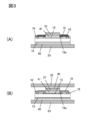
- (A) and (B) are sectional views of the semiconductor device in each step for explaining the manufacturing method of the semiconductor device 100 illustrated in FIG.
- (A) and (B) are cross-sectional views of the semiconductor device in each step following FIG.
- FIG. 5 is a cross-sectional view of a second embodiment of the semiconductor device of the present invention. It is sectional drawing for demonstrating the action which a high electric field is applied to the void existing in a sealing resin, and partial discharge is generated,
- (A) is sectional drawing of the semiconductor device 100R of a comparative example,
- (B) is Sectional drawing of the semiconductor device of this embodiment.
- FIG. 6 An enlarged exploded perspective view of the semiconductor device shown in FIG. 6 is a cross-sectional view of the semiconductor device shown in FIG. 6, where FIG. 6A is a cross-sectional view before resin sealing, and FIG. 6B is a cross-sectional view after resin sealing.
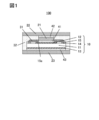
- FIG. 1 is a cross-sectional view of a first embodiment of the semiconductor device of the present invention.
- the semiconductor device 100 includes a semiconductor element 10.
- the semiconductor element 10 is, for example, a SiC (silicon carbide) MOS FET (Metal-Oxide-Semiconductor Field effect transistor).
- the semiconductor element 10 has a semiconductor substrate 11, a source electrode 12, a drain electrode 13, an internal wiring 14, and a first insulating layer 15. Although not shown in FIG. 1, the semiconductor element 10 has a gate electrode 17 (see FIG. 7).
- the semiconductor device 100 includes a semiconductor element 10, a relay conductor 21, a front surface side conductor 22, a back surface side conductor 23, a second insulating layer 31, and a sealing resin 32.
- the first insulating layer 15 is an insulating film provided inside the semiconductor substrate 11 to protect the impurity region for forming the semiconductor element and the internal wiring 14, and is formed of an inorganic material such as silicon oxide or silicon nitride. Has been done.
- the first insulating layer 15 is provided with an opening 15a (see also FIG. 2B).
- the source electrode 12 is formed slightly larger than the opening 15a of the first insulating layer 15, and the inside of the peripheral edge of the source electrode 12 is exposed from the opening 15a of the first insulating layer 15.
- the first insulating layer 15 is formed of, for example, a resin such as polyimide or polybenzoxador.
- the first insulating layer 15 is formed by a semiconductor device manufacturer, and its thickness is generally about several ⁇ m.
- the relay conductor 21 has an area slightly smaller than the opening 15a of the first insulating layer 15, and is joined to the entire surface of the source electrode 12 exposed from the opening 15a of the first insulating layer 15 by the bonding layer 41. ing.
- the bonding layer 41 has substantially the same area as the relay conductor 21. Therefore, a gap G (see FIG. 2B) is formed between the peripheral edge of the bonding layer 41 and the peripheral edge of the opening 15a of the first insulating layer 15.
- the relay conductor 21 can be formed of a copper-based metal. Further, the relay conductor 21 can be formed by using a clad material such as CIC (Copper Invar Copper). Invar (registered trademark) is an alloy of iron and nickel and is a material with a low coefficient of thermal expansion. Therefore, by forming the relay conductor 21 from a material containing Invar, even if the semiconductor element 10 becomes hot during driving, It is possible to suppress peeling from the sealing resin 32.
- CIC Copper Invar Copper
- the second insulating layer 31 is formed on the first insulating layer 15.
- the second insulating layer 31 is not formed on the entire surface of the first insulating layer 15, and the peripheral edge side of the first insulating layer 15 is exposed from the second insulating layer 31.
- the second insulating layer 31 is also filled in the gap G between the peripheral edge of the bonding layer 41 and the peripheral edge of the opening 15a of the first insulating layer 15, and the peripheral edge of the bonding layer 41 and the relay conductor 21 are also filled. It is in contact with the peripheral edge of the region near the joint layer 41 side of the above.
- the second insulating layer 31 is formed by coating using a potting method, a printing method, or the like.
- the second insulating layer 31 is formed of, for example, a resin such as polyamideimide, polyimide, polyetheramideimide, or polyetheramide.
- the first insulating layer 15 and the second insulating layer 31 may be formed of the same resin.
- the second insulating layer 31 is about several tens of ⁇ m, and is preferably thicker than the thickness of the first insulating layer 15.
- the surface-side conductor 22 has a surface area of the semiconductor element 10, that is, an area larger than the area of the first insulating layer 15 in a plan view.
- the surface side conductor 22 is joined to the relay conductor 21 by the joining layer 42.
- the bonding layer 42 has substantially the same area as the relay conductor 21.
- the surface side conductor 22 can be formed of a copper-based metal or an aluminum-based metal.
- the back surface side conductor 23 is bonded to the drain electrode 13 provided on the back surface side facing the source electrode 12 of the semiconductor substrate 11 by the bonding layer 43.
- the back surface side conductor 23 has the same area as the front surface side conductor 22.
- the sealing resin 32 is filled between the front surface side conductor 22 and the back surface side conductor 23. That is, the peripheral side surface of the semiconductor element 10, the second insulating layer 31, and the peripheral side surface of the relay conductor 21 are sealed with the sealing resin 32.
- the back surface side conductor 23 can be formed of a copper-based metal or an aluminum-based metal.
- Solder or sintered metal material can be used as the bonding layers 41 to 43.
- the sealing resin 32 an epoxy resin or the like can be used.
- a molding method such as transfer molding is suitable, but a printing method such as a potting method, silk printing, sealing printing, inkjet printing, thermal transfer printing or the like may be used.
- FIG. 5 is a cross-sectional view for explaining the action of applying a high electric field to the voids existing in the sealing resin to generate a partial discharge.
- FIG. 5A is a cross-sectional view showing a void generated in the sealing resin of the semiconductor device 100R of the comparative example
- FIG. 5B is a void generated in the sealing resin of the semiconductor device 100 of the present embodiment. It is sectional drawing which shows.
- the semiconductor device 100R of the comparative example shown in FIG. 5A does not have the relay conductor 21 of the semiconductor device 100 of the present embodiment.
- the surface-side conductor 22R has a protruding portion 25 facing the portion of the source electrode 12 exposed from the opening 15a of the first insulating layer 15.
- the protruding portion 25 is integrally molded with the surface side conductor 22R. That is, after the protruding portion 25 and the source electrode 12 are joined by the joining layer 41, the peripheral region of the gap G between the inner peripheral edge portion of the opening 15a of the first insulating layer 15 and the joining layer 41 is sealed. It is covered with the surface side conductor 22R via the resin 32.
- the second insulating layer 31R when the second insulating layer 31R is applied on the first insulating layer 15 before the sealing resin 32 is filled between the front surface side conductor 22R and the back surface side conductor 23, the front surface side conductor 22R becomes an obstacle. Therefore, it is difficult to form the second insulating layer 31R so as to be in contact with the peripheral edge of the bonding layer 41 or the peripheral edge of the protruding portion 25. That is, the gap G between the inner peripheral edge of the opening 15a of the first insulating layer 15 and the bonding layer 41 is not covered by the first insulating layer 15 or the second insulating layer 31R. In FIG.
- the second insulating layer 31R when the second insulating layer 31R is filled before the surface side conductor 22R is joined to the source electrode 12, the region where the surface side conductor 22R of the source electrode 12 is joined (surface side conductor joining region).
- a step is required to prevent the second insulating layer 31R) from invading the surface. Further, in this step, it is necessary to provide a slight gap G between the surface side conductor bonding region of the source electrode 12 and the inner peripheral edge portion of the opening 15a of the first insulating layer 15, and the insulating material is provided in this slight gap G. can not be sufficiently filled, the sealing resin degradation due to a high electric field of voids a V can not be avoided.
- a high electric field is generated around the source electrode 12.
- a SiC MOS FET produces a high electric field with a dielectric breakdown electric field strength about 10 times that of a Si MOSFET.
- voids A V is present in the sealing resin 32 near the source electrode 12
- a high electric field is concentrated on the void A V, partial discharge may occur. If the state in which the partial discharge occurs continues, the sealing resin 32 deteriorates, and finally dielectric breakdown occurs and the semiconductor element 10 fails.
- a sealing resin by molding method is difficult to fill, there is a high probability that voids A V occurs.
- the semiconductor device 100 of the present embodiment has a relay conductor 21 provided between the source electrode 12 and the surface side conductor 22. Therefore, in a state where the relay conductor 21 is bonded to the source electrode 12 by the bonding layer 41, the second insulating layer 31 is attached to the peripheral portion of the first insulating layer 15 before the surface side conductor 22 is bonded to the relay conductor 21. It can be filled in the gap G between the bonding layer 41 and the bonding layer 41.
- voids A V is present in the second insulating layer 31 by a sealing resin 32 in a state where the gap G is covered between the peripheral edge portion of the first insulating layer 15 and the bonding layer 41, generated in the source electrode 12 periphery a high electric field is divided voltage and half to be applied to the voltage and the second insulating layer 31 applied to the void a V.
- Voltage applied to the voids A V is the air layer is related to the ratio of the dielectric constant of the second insulating layer 31 for dielectric constant, and the void A V thickness and the second insulating layer 31 thickness of the air layer.
- the thickness increases in the second insulating layer 31, the thickness of the void A V decreases, the voltage to focus the void A V decreases. Therefore, by setting the thickness of the second insulating layer 31 to a predetermined thickness or more, the voltage applied to the void A V can be smaller than the partial discharge inception voltage.
- the second insulating layer 31 has a predetermined thickness or more, then the front side conductor 22 is joined to the relay conductor 21 by the joining layer 42, and the sealing resin is formed between the front side conductor 22 and the back side conductor 23. If 32 filled with, be void a V is generated in the sealing resin 32, it is possible to suppress the partial discharge occurs. Next, a method of manufacturing the semiconductor device 100 will be described.
- FIGS. 3 (A) and 3 (B) are cross-sectional views of the semiconductor device in each step for explaining the manufacturing method of the semiconductor device 100 illustrated in FIG. 1, and FIGS. 3 (A) and 3 (B).
- B) is a cross-sectional view of the semiconductor device in each step following FIG.
- the semiconductor element 10 is prepared. As described above, the semiconductor element 10 has a semiconductor substrate 11, a source electrode 12, a drain electrode 13, an internal wiring 14, and a first insulating layer 15. Then, as shown in FIG. 2A, the drain electrode 13 of the semiconductor element 10 and the back surface side conductor 23 are joined by the joining layer 43.
- solder or a sintered metal material can be used as the bonding layer 43.
- the sintered metal material has a powder or paste form, and becomes a sintered metal by heating.
- As the sintered metal material it is preferable to use a sintered metal bonding paste containing copper or silver.
- a bonding layer 43 is interposed between the drain electrode 13 of the semiconductor element 10 and the back surface side conductor 23, and the bonding is performed by thermocompression bonding.
- the source electrode 12 of the semiconductor element 10 and the relay conductor 21 are joined by the joining layer 41.
- the bonding layer 41 the same layer as the bonding layer 43 is used.
- a bonding layer 41 is interposed between the source electrode 12 of the semiconductor element 10 and the relay conductor 21 and bonded by thermocompression bonding.
- the bonding layer 41 that joins the source electrode 12 of the semiconductor element 10 and the relay conductor 21 is provided in the opening 15a of the first insulating layer 15 of the semiconductor element 10. That is, the bonding layer 41 is smaller than the opening 15a of the first insulating layer 15 of the semiconductor element 10. Therefore, a gap G is formed between the peripheral edge of the first insulating layer 15 and the bonding layer 41.
- FIG. 2 (A) and the process of FIG. 2 (B) may be reversed. Moreover, you may carry out in the same process.
- the drain electrode 13 of the semiconductor element 10 and the back surface side conductor 23 are interposed with the bonding layer 43, and the bonding layer 41 is interposed between the source electrode 12 of the semiconductor element 10 and the relay conductor 21. , In this state, the whole is thermocompression bonded.
- the second insulating layer 31 is applied on the first insulating layer 15.
- the second insulating layer 31 is formed in the peripheral edge of the bonding layer 41 in the gap G (see FIG. 2B) between the peripheral edge of the bonding layer 41 and the peripheral edge of the opening 15a of the first insulating layer 15. Filled to touch.
- the second insulating layer 31 may be provided so as to be in contact with the lower end portion side of the relay conductor 21, in other words, the peripheral edge portion on the bonding layer 41 side.
- a potting method using a dispenser or a printing method can be used for forming the second insulating layer 31.
- As a printing method silk printing, sealing printing, inkjet printing, thermal transfer printing and the like can be applied.
- the surface side conductor 22 is joined to the relay conductor 21 by the joining layer 42.
- the bonding layer 42 the same layer as the bonding layers 41 and 43 is used.
- a bonding layer 42 is interposed between the relay conductor 21 and the surface side conductor 22 and bonded by thermocompression bonding.
- the sealing resin 32 is filled between the front surface side conductor 22 and the back surface side conductor 23.
- the semiconductor device 100 shown in FIG. 1 is formed in which the peripheral side surface of the semiconductor element 10, the second insulating layer 31, and the peripheral side surface of the relay conductor 21 are sealed with the sealing resin 32.
- the transfer molding method is suitable for forming the sealing resin 32, but a potting method or a printing method may also be used.
- the semiconductor device 100 is joined to a semiconductor element 10 having a first insulating layer 15 having an opening 15a and a source electrode (surface electrode) 12 exposed from the opening 15a of the first insulating layer 15 and the source electrode 12.
- the second insulation is provided so as to cover at least a part of the first insulating layer 15 and the joint layer 41 that joins the relay conductor 21 and the source electrode 12 and the relay conductor 21 so as to be in contact with at least the periphery of the joint layer 41.
- the layer 31 includes a surface-side conductor (conductor) 22 connected to the relay conductor 21, and a sealing resin 32 filled between the surface-side conductor 22 and the second insulating layer 31.
- the source electrode 12 exposed from the opening 15a of the first insulating layer 15 is covered with the second insulating layer 31 provided in contact with the periphery of the bonding layer 41. Therefore, even if there is a void A V in the sealing resin 32, the occurrence of partial discharge can be suppressed, it is possible to suppress the deterioration of the sealing resin 32.
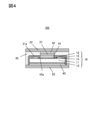
- FIG. 4 is a cross-sectional view of a second embodiment of the semiconductor device of the present invention.
- the semiconductor device 100 of the second embodiment has a structure in which the second insulating layer 31a extends on the outer peripheral side surface of the semiconductor element 10 and is in contact with the back surface side conductor 23.
- the second insulating layer 31 is formed only on the front surface side of the semiconductor element 10, and is not extended so as to be in contact with the back surface side conductor 23.
- the joining layer 41 may be melted by heating during thermocompression bonding, and the relay conductor 21 may be misaligned.
- the second insulating layer 31a extends to a position where it contacts the back surface side conductor 23. Since the second insulating layer 31a is in contact with the relay conductor 21, even if the bonding layer 41 is melted by heating during thermocompression bonding, the movement of the relay conductor 21 is restricted by the second insulating layer 31a in contact with the back surface side conductor 23. Will be done.
- the other configurations of the second embodiment are the same as those of the first embodiment, and the corresponding configurations are designated by the same reference numerals and the description thereof will be omitted.
- the second embodiment also has the same effect as that of the first embodiment. Further, according to the second embodiment, it is possible to suppress the misalignment of the relay conductor 21 when the surface side conductor 22 is joined to the relay conductor 21.
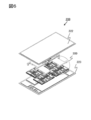
- FIG. 6 is an exploded perspective view of a third embodiment of the semiconductor device of the present invention.
- the semiconductor device 200 includes four semiconductor devices 300, an outer front surface side conductor 222, and an outer back surface side conductor 223.
- the four semiconductor devices 300 are arranged in a matrix with two rows in the horizontal direction and two columns in the vertical direction, separated from each other.
- the outer front surface side conductor 222 and the outer back surface side conductor 223 each have a size that covers the entire region of the four semiconductor devices 300 arranged in a matrix. All four semiconductor devices 300 have the same structure.
- the two semiconductor devices 300 each have an upper arm circuit, and the remaining two semiconductor devices 300 each have a lower arm circuit.
- the semiconductor device 300 having the upper arm circuit and the semiconductor device 300 having the lower arm circuit are connected in series to form an upper and lower arm series circuit.
- a power conversion device capable of obtaining AC outputs having different phases can be configured from the connection portion between the upper arm circuit and the lower arm circuit.
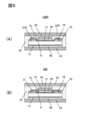
- FIG. 7 is an enlarged exploded perspective view of the semiconductor device shown in FIG. 6,
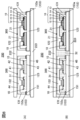
- FIG. 8 is a cross-sectional view of the semiconductor device shown in FIG. 6, and
- FIG. 8 (A) is a cross section before resin sealing.
- FIG. 8 (B) is a cross-sectional view after resin sealing.
- the semiconductor device 300 includes four semiconductor elements 10, a front surface side conductor 122, and a back surface side conductor 123.
- the four semiconductor elements 10 are arranged in a matrix with two rows in the horizontal direction and two columns in the vertical direction, separated from each other. That is, the semiconductor device 300 is configured as a 4in1 package.
- the front surface side conductor 122 and the back surface side conductor 123 each have a size that covers the entire region of the four semiconductor elements 10 arranged in a matrix.
- Each of the four semiconductor elements 10 has the same structure as the semiconductor element of the first embodiment. That is, as shown in FIG. 8, the semiconductor element 10 has a semiconductor substrate 11, a source electrode 12, a drain electrode 13, an internal wiring 14, and a first insulating layer 15. As shown in FIG. 8, a relay conductor 21 is bonded to the source electrode 12 of each semiconductor element 10 via a bonding layer 41. Further, on the first insulating layer 15 of each semiconductor element 10, a second insulating layer 31 is formed which is in contact with the peripheral edge of the bonding layer 41 and the peripheral region of the relay conductor 21 near the bonding layer 41 side.
- the surface-side conductor 122 is attached to a rectangular body covering the four semiconductor elements 10 and to the tips of legs extending from each of the four corners of the rectangular body. It has a sense connection portion 131 projecting toward the back surface side conductor 123 side.
- the sense connection portion 131 has a quadrangular prism shape and has a large cross-sectional area as compared with the bonding wire. The reason why the sense connection portion 131 has a large cross-sectional area is to secure the strength to withstand the load acting on the front surface side conductor 122 and the back surface side conductor 123 and to reduce the inductance.
- the back surface side conductor 123 is a member corresponding to the back surface side conductor 23 of the first embodiment, but in the third embodiment, the four semiconductor elements 10 have a size of being bonded via the bonding layer 43.
- the back surface side conductor 123 is provided with an insulating layer 151 on the entire surface excluding the region where the four semiconductor elements 10 are joined. Resin or ceramic can be used for the insulating layer 151.
- a gate wiring 152 and a sense wiring 153 are provided on the insulating layer 151 formed on the back surface side conductor 123.
- the gate wiring 152 and the sense wiring 153 are connected to a control unit (not shown).
- the control unit applies a voltage to the source electrode 12 of the semiconductor element 10 via the gate wiring 152 with the connection of the semiconductor element 10 to the source electrode 12 via the sense wiring 153 as ground, that is, as a reference potential. ..
- the reason for increasing the cross-sectional area of the sense connection portion 131 is to reduce the inductance, but to be precise, it is to reduce the inductance in the connection of the semiconductor element 10 with the source electrode 12 via the sense wiring 153. ..
- the gate wiring 152 is placed on the insulating layer 151 provided on the back surface side conductor 123 between the two pairs of semiconductor elements 10 separated to the left and right, in other words, the back surface side conductor 123. It is formed so as to extend in the vertical direction of the back surface side conductor 123 at the center of the left side and the right side of the above.
- the gate electrode 17 of each semiconductor element 10 is connected to the gate wiring 152 by a bonding wire 161.
- the sense wiring 153 is formed so as to surround the outside of the gate wiring 152 with a slight gap from the gate wiring 152.
- the sense wiring 153 extends in the vertical direction of the back surface side conductor 123 and extends along the upper side side surface and the lower side side surface of the back surface side conductor 123 to the vicinity of the corner portion of the back surface side conductor 123. Has a part.
- the sense wiring 153 has a sense contact region 153a to which the lower end surface of the sense connection portion 131 of the surface side conductor 122 is joined in the vicinity of each corner portion.
- the sense contact area 153a is a part of the sense wiring 153, and actually there is no partition line indicating the area. However, in FIG. 7, the sense contact area 153a is illustrated by a rectangular solid line for easy understanding. There is.
- the surface-side conductor 122 is bonded to the source electrode 12 of each semiconductor element 10 by the bonding layer 42 (see FIGS. 8A and 8B). Therefore, the sense wiring 153 is connected to the source electrode 12 of each semiconductor element 10 via the surface side conductor 122.
- the four semiconductor elements 10 are arranged close to each other, the heat emitted from each semiconductor element 10 is concentrated in a narrow region, and the back surface side conductor 123 becomes hot. Therefore, as shown in FIG. 7, the four semiconductor elements 10 are arranged so as to be separated from each other by a predetermined width or more so that heat is not concentrated. However, if the semiconductor elements 10 are arranged apart from each other by a predetermined width or more, the area of the back surface side conductor 123, in other words, the semiconductor device 300 becomes large. Therefore, by routing the gate wiring 152 and the sense wiring 153 in the central space where the semiconductor element 10 is separated, the space is effectively utilized and the area of the back surface side conductor 123 is reduced.
- the sense contact region 153a to which the lower end surface of the sense connection portion 131 of the surface side conductor 122 is joined is outside the rectangular outer peripheral region in which the four semiconductor elements 10 are arranged. Is located in. Therefore, the inductance in the connection of the semiconductor element 10 with the source electrode 12 via the sense wiring 153 can be reduced.
- the four semiconductor devices 300 constituting the semiconductor device 200 shown in FIG. 6 are arranged between the outer front surface side conductor 222 and the outer back surface side conductor 223.
- the surface-side conductor 122 of each semiconductor device 300 is joined to the outer surface-side conductor 222 by a bonding layer 44.
- the back surface side conductor 123 of each semiconductor device 300 is joined to the outer back surface side conductor 223 by the bonding layer 45.
- the bonding layers 44 and 45 can be formed by using the same material as the bonding layers 41 to 43.
- the state shown in FIG. 8A is a state in which the sealing resin 32 is not filled in the four semiconductor devices 300 constituting the semiconductor device 200. That is, each semiconductor element 10, the second insulating layer 31, and the like are not sealed by the sealing resin 32. However, on the first insulating layer 15 of each semiconductor element 10, a second insulating layer 31 is formed in contact with the peripheral edge of the bonding layer 41 and the peripheral region of the relay conductor 21 near the bonding layer 41 side. Therefore, in this state, a high electric field application test in which a high electric field is applied to the source electrode 12 can be performed. By applying a high electric field to the source electrode 12, it is inspected whether partial discharge is generated, the semiconductor element 10 is damaged, or the characteristics are deteriorated, and defective products are removed or repaired. can do. As a result, the productivity can be improved as compared with the inspection after the resin is sealed.
- a sealing resin 32 is filled between the outer front surface side conductor 222 and the outer back surface side conductor 223, and the peripheral side surface of each semiconductor element 10, the second insulating layer 31, and the peripheral side surface of the relay conductor 21 are filled. Is sealed with the sealing resin 32.
- the high electric field application test may be performed in the state of FIG. 8 (b), may be performed in the state of FIG. 8 (a), and may be performed again in the state of FIG. 8 (b).
- the sense wiring 153 and the source electrode 12 are exemplified as a structure in which the sense wiring 153 and the source electrode 12 are connected by a sense connection portion 131 integrally provided on the surface side conductor 122.
- the sense wiring 153 and the source electrode 12 may be connected by a bonding wire.
- the semiconductor device 300 is exemplified as a 4in1 package in which four arm circuits are integrated.
- the semiconductor device 300 may be a package in which a plurality of arm circuits are integrated, and can be widely applied to an N (N ⁇ 2) in 1 package.
- the switching element is exemplified as a MOS FET.
- MOS FET Metal Organic Switches
- IGBT Insulated Gate Bipolar Transistor
- a SiC (silicon carbide) MOS FET is preferred as the switching element.
- the present invention can be applied not only to silicon carbide but also to semiconductor devices using gallium nitride, gallium oxide, and diamond as a base material.
- the present invention can also be applied to ordinary Si MOS FETs.
Landscapes
- Structures Or Materials For Encapsulating Or Coating Semiconductor Devices Or Solid State Devices (AREA)
- Cooling Or The Like Of Semiconductors Or Solid State Devices (AREA)
Abstract
半導体装置100は、開口部15aを有する第一絶縁層15および第一絶縁層15の開口部15aから露出するソース電極12を有する半導体素子10と、ソース電極12に接合された中継導体21と、ソース電極12と中継導体21とを接合する接合層41と、第一絶縁層15aの少なくとも一部を覆い、少なくとも接合層41の周囲に接して設けられた第二絶縁層31と、中継導体21に接続された表面側導体22と、表面側導体22と第二絶縁層31との間に充填された封止樹脂32と、を備える。これによって、ボイドが存在しても、部分放電の発生が抑制される半導体装置を提供する。
Description
本発明は、半導体装置およびその製造方法に関する。
モータ等を駆動する電力変換部を有するパワー半導体装置として、パワー半導体素子を一対の金属板により挟んで、金属板間に樹脂を充填して半導体素子を封止する構造を有するものがある。より詳細には、半導体素子の一方の電極に金属ブロックを接合し、この金属ブロックを一方の金属板に接続し、半導体素子の他方の電極を他方の金属板に接続する。各金属板の面積は、半導体素子の表裏面の面積より大きく形成されており、この一対の金属板間に、トランスファーモールド法等のモールド法により、樹脂を充填して半導体素子を封止する(例えば、特許文献1参照)。
モールド法により形成する封止樹脂には、ボイド(空隙)等の欠陥部が生じ易い。パワー半導体装置では、パワー半導体素子に高電圧が印加されるため、封止樹脂にボイド等の欠陥部が存在すると、その欠陥部に電界が集中し、部分放電が発生する可能性がある。部分放電が発生した状態が続くと、封止樹脂が劣化し、最終的に絶縁破壊してパワー半導体装置が故障する虞がある。
本発明の第一の態様によると、半導体装置は、開口部を有する第一絶縁層および前記第一絶縁層の前記開口部から露出する表面電極を有する半導体素子と、前記表面電極に接合された中継導体と、前記表面電極と前記中継導体とを接合する接合層と、前記第一絶縁層の少なくとも一部を覆い、少なくとも前記接合層の周囲に接して設けられた第二絶縁層と、前記中継導体に接続された導体と、前記導体と前記第二絶縁層との間に充填された封止樹脂と、を備える。
本発明の第二の態様によると、半導体装置は、開口部を有する第一絶縁層および前記第一絶縁層の前記開口部から露出する表面電極を有する複数の半導体素子と、前記各半導体素子の前記表面電極に接合された中継導体と、前記各表面電極と前記各中継導体を接合する接合層と、前記各第一絶縁層の少なくとも一部を覆い、少なくとも前記各接合層の周囲に接して設けられた第二絶縁層と、前記各中継導体を接続する導体と、を備える。
本発明の第三の態様によると、半導体装置の製造方法は、開口部を有する第一絶縁層および前記第一絶縁層の前記開口部から露出する表面電極を有する半導体素子を準備することと、前記表面電極と中継導体とを接合層により接合することと、前記第一絶縁層の少なくとも一部を覆い、少なくとも前記接合層の周囲に接する第二絶縁層を設けることと、前記中継導体に導体を接続することと、前記導体と前記第二絶縁層との間に封止樹脂を充填することと、を含む。
本発明によれば、ボイドが存在しても、部分放電の発生が抑制される。
以下、図面を参照して本発明の実施形態を説明する。以下の記載および図面は、本発明を説明するための例示であって、説明の明確化のため、適宜、省略および簡略化がなされている。本発明は、他の種々の形態でも実施する事が可能である。特に限定しない限り、各構成要素は単数でも複数でも構わない。
図面において示す各構成要素の位置、大きさ、形状、範囲などは、発明の理解を容易にするため、実際の位置、大きさ、形状、範囲などを表していない場合がある。このため、本発明は、必ずしも、図面に開示された位置、大きさ、形状、範囲などに限定されない。
図面において示す各構成要素の位置、大きさ、形状、範囲などは、発明の理解を容易にするため、実際の位置、大きさ、形状、範囲などを表していない場合がある。このため、本発明は、必ずしも、図面に開示された位置、大きさ、形状、範囲などに限定されない。
-第1の実施形態-
以下、図1~図3を参照して、本発明の第1の実施形態を説明する。
図1は、本発明の半導体装置の第1の実施形態の断面図である。
半導体装置100は、半導体素子10を備えている。半導体素子10は、例えば、SiC(シリコンカーバイト)MOS FET(Metal-Oxide-Semiconductor Field effecttransistor)である。半導体素子10は、半導体基板11と、ソース電極12と、ドレイン電極13と、内部配線14と、第一絶縁層15を有する。なお、図1には、図示しないが、半導体素子10は、ゲート電極17(図7参照)を有する。半導体装置100は、半導体素子10と、中継導体21と、表面側導体22と、裏面側導体23と、第二絶縁層31と、封止樹脂32を有する。
第一絶縁層15は、半導体基板11内部に形成された半導体素子形成用の不純物領域および内部配線14を保護するために設けられた絶縁膜であり、酸化シリコンまたは窒化シリコン等の無機材料により形成されている。第一絶縁層15には、開口部15a(図2(B)も参照)が設けられている。ソース電極12は、第一絶縁層15の開口部15aより少し大きく形成されており、ソース電極12の周縁部の内側が第一絶縁層15の開口部15aから露出している。第一絶縁層15は、例えば、ポリイミドまたはポリベンゾオキサドール等の樹脂により形成される。第一絶縁層15は、半導体素子メーカーにより形成されており、その厚さは、一般的に、数μm程度とされている。
中継導体21は、第一絶縁層15の開口部15aより少し小さい面積を有し、接合層41により、ソース電極12の、第一絶縁層15の開口部15aから露出した部分の全面に接合されている。接合層41は、中継導体21とほぼ同じ面積を有する。従って、接合層41の周縁部と第一絶縁層15の開口部15aの周縁部との間には隙間G(図2(B)参照)が形成されている。中継導体21は、銅系金属により形成することができる。また、中継導体21は、CIC(Copper Invar Copper)等のクラッド材を用いて形成することができる。インバー(登録商標)は、鉄とニッケルの合金であり、低熱膨張率の材料であるので、インバーを含む材料により中継導体21を形成することにより、駆動時に半導体素子10が高温となっても、封止樹脂32との剥離を抑制することができる。
第二絶縁層31は、第一絶縁層15上に形成されている。第二絶縁層31は、第一絶縁層15の全面には形成されておらず、第一絶縁層15の周縁部側は、第二絶縁層31から露出している。第二絶縁層31は、接合層41の周縁部と第一絶縁層15の開口部15aの周縁部との間の隙間G内にも充填されており、接合層41の周縁部および中継導体21の接合層41側近傍領域の周縁部に接している。第二絶縁層31は、後述するように、ポッティング法または印刷法等を用いた塗布により形成される。第二絶縁層31は、例えば、ポリアミドイミド、ポリイミド、ポリエーテルアミドイミド、ポリエーテルアミド等の樹脂で形成される。第一絶縁層15と第二絶縁層31を、同じ樹脂により形成してもよい。第二絶縁層31は、数十μm程度であり、第一絶縁層15の厚さより厚くすることが好ましい。
表面側導体22は、半導体素子10の表面面積、すなわち、第一絶縁層15の平面視での面積よりも大きい面積を有する。表面側導体22は、接合層42により中継導体21に接合されている。接合層42は、中継導体21とほぼ同じ面積を有する。表面側導体22は、銅系金属またはアルミニウム系金属により形成することができる。
裏面側導体23は、接合層43により、半導体基板11のソース電極12と対向する裏面側に設けられたドレイン電極13に接合されている。裏面側導体23は、表面側導体22と同じ面積を有する。封止樹脂32は、表面側導体22と裏面側導体23との間に充填されている。つまり、半導体素子10の周側面、第二絶縁層31、中継導体21の周側面は、封止樹脂32により封止されている。裏面側導体23は、銅系金属またはアルミニウム系金属により形成することができる。
接合層41~43として、はんだや焼結金属材料を用いることができる。
封止樹脂32としては、エポキシ樹脂等を用いることができる。封止樹脂32による封止は、トランスファーモールド等のモールド法等が適しているが、ポッティング法や、シルク印刷、シーリング印刷、インクジェット印刷、熱転写印刷等の印刷法を用いてもよい。
次に、上記実施形態の半導体装置100における、ボイドの存在に伴う封止樹脂の劣化抑制作用について説明する。
封止樹脂32としては、エポキシ樹脂等を用いることができる。封止樹脂32による封止は、トランスファーモールド等のモールド法等が適しているが、ポッティング法や、シルク印刷、シーリング印刷、インクジェット印刷、熱転写印刷等の印刷法を用いてもよい。
次に、上記実施形態の半導体装置100における、ボイドの存在に伴う封止樹脂の劣化抑制作用について説明する。
図5は、封止樹脂に存在するボイドに高電界が印加され、部分放電が発生する作用を説明するための断面図である。図5(A)は、比較例の半導体装置100Rの封止樹脂に発生するボイドを示す断面図であり、図5(B)は、本実施形態の半導体装置100の封止樹脂に発生するボイドを示す断面図である。
図5(A)に図示される比較例の半導体装置100Rは、本実施形態の半導体装置100の中継導体21を有していない。
半導体装置100Rでは、表面側導体22Rは、ソース電極12の、第一絶縁層15の開口部15aから露出した部分に対向する突出部25を有している。突出部25は、表面側導体22Rと一体成形されている。すなわち、突出部25とソース電極12とを接合層41により接合した後では、第一絶縁層15の開口部15aの内周縁部と接合層41との間の隙間Gの周辺領域は、封止樹脂32を介して表面側導体22Rにより覆われている。
図5(A)に図示される比較例の半導体装置100Rは、本実施形態の半導体装置100の中継導体21を有していない。
半導体装置100Rでは、表面側導体22Rは、ソース電極12の、第一絶縁層15の開口部15aから露出した部分に対向する突出部25を有している。突出部25は、表面側導体22Rと一体成形されている。すなわち、突出部25とソース電極12とを接合層41により接合した後では、第一絶縁層15の開口部15aの内周縁部と接合層41との間の隙間Gの周辺領域は、封止樹脂32を介して表面側導体22Rにより覆われている。
このため、表面側導体22Rと裏面側導体23との間に封止樹脂32を充填する前に、第一絶縁層15上に第二絶縁層31Rを塗布する場合、表面側導体22Rが邪魔になり、第二絶縁層31Rを接合層41の周縁部や突出部25の周縁部に接するように形成することは困難である。つまり、第一絶縁層15の開口部15aの内周縁部と接合層41との間の隙間Gは、第一絶縁層15によっても、第二絶縁層31Rによっても覆われない状態となる。
なお、図5(A)において、表面側導体22Rをソース電極12に接合する前に第2絶縁層31Rを充填する場合、ソース電極12の表面側導体22Rを接合する領域(表面側導体接合領域に第2絶縁層31R)が侵入しないようにする工程が必要である。また、この工程では、ソース電極12の表面側導体接合領域と第1絶縁層15の開口15aの内周縁部との間に僅かな隙間Gを設ける必要があり、この僅かな隙間Gに絶縁材が十分に充填できず、ボイドAVの高電界による封止樹脂劣化は避けられない。
なお、図5(A)において、表面側導体22Rをソース電極12に接合する前に第2絶縁層31Rを充填する場合、ソース電極12の表面側導体22Rを接合する領域(表面側導体接合領域に第2絶縁層31R)が侵入しないようにする工程が必要である。また、この工程では、ソース電極12の表面側導体接合領域と第1絶縁層15の開口15aの内周縁部との間に僅かな隙間Gを設ける必要があり、この僅かな隙間Gに絶縁材が十分に充填できず、ボイドAVの高電界による封止樹脂劣化は避けられない。
MOS FET等では、ソース電極12周辺部には高電界が発生する。特に、SiC MOS FETでは、Si MOSFETの10倍程度の絶縁破壊電界強度の高電界が生じる。ソース電極12周辺の封止樹脂32にボイドAVが存在すると、ボイドAVに高電界が集中し、部分放電が発生する可能性がある。部分放電が発生した状態が続くと、封止樹脂32が劣化し、最終的に絶縁破壊して半導体素子10が故障する。
特に、突出部25がソース電極12に接合されているような狭い空間には、モールド法による封止樹脂は充填され難く、ボイドAVが発生する確率が高い。
特に、突出部25がソース電極12に接合されているような狭い空間には、モールド法による封止樹脂は充填され難く、ボイドAVが発生する確率が高い。
本実施形態の半導体装置100は、図5(B)に図示するように、ソース電極12と表面側導体22との間に設けられた中継導体21を有している。このため、接合層41により、ソース電極12に中継導体21を接合した状態で、表面側導体22を中継導体21に接合する前に、第二絶縁層31を、第一絶縁層15の周縁部と接合層41との間の隙間G内に充填することができる。第二絶縁層31により第一絶縁層15の周縁部と接合層41との間の隙間Gが覆われた状態で封止樹脂32にボイドAVが存在すると、ソース電極12周辺部に発生する高電界は、ボイドAVに印加される電圧と第二絶縁層31に印加される電圧とに分圧される。
空気層であるボイドAVに加わる電圧は、空気層の誘電率に対する第二絶縁層31の比誘電率、およびボイドAVの厚さと第二絶縁層31の厚さとの比に関連する。第二絶縁層31の厚さが大きくなり、ボイドAVの厚さが小さくなると、ボイドAVに集中する電圧が小さくなる。このため、第二絶縁層31の厚さを所定の厚さ以上とすることにより、ボイドAVに加わる電圧を部分放電開始電圧より小さくすることができる。従って、第二絶縁層31を所定の厚さ以上とすれば、この後、接合層42により中継導体21に表面側導体22を接合し、表面側導体22と裏面側導体23間に封止樹脂32を充填した場合、封止樹脂32にボイドAVが発生しても、部分放電が発生するのを抑制することができる。
次に、半導体装置100の製造方法を説明する。
次に、半導体装置100の製造方法を説明する。
図2(A)、図2(B)は、図1に図示された半導体装置100の製造方法を説明するための各工程における半導体装置の断面図であり、図3(A)、図3(B)は、図2に続く各工程における半導体装置の断面図である。
先ず、半導体素子10を準備する。 上述したように、半導体素子10は、半導体基板11と、ソース電極12と、ドレイン電極13と、内部配線14と、第一絶縁層15とを有する。
そして、図2(A)に図示するように、半導体素子10のドレイン電極13と裏面側導体23とを接合層43により接合する。接合層43として、上述したように、はんだ、または焼結金属材料を用いることができる。焼結金属材料は、粉末やペースト状を有しており、加熱により焼結金属となる。焼結金属材料としては、銅や銀を含む焼結金属接合ペーストを用いることが好ましい。半導体素子10のドレイン電極13と裏面側導体23との間に接合層43を介在させ、熱圧着することにより接合する。
次に、図2(B)に図示するように、半導体素子10のソース電極12と中継導体21とを接合層41により接合する。接合層41として、接合層43と同様なものを用いる。
半導体素子10のソース電極12と中継導体21との間に接合層41を介在させ、熱圧着することにより接合する。半導体素子10のソース電極12と中継導体21とを接合する接合層41は、半導体素子10の第一絶縁層15の開口部15a内に設けられる。つまり、接合層41は、半導体素子10の第一絶縁層15の開口部15aより小さい。このため、第一絶縁層15の周縁部と接合層41との間には、隙間Gが形成される。
半導体素子10のソース電極12と中継導体21との間に接合層41を介在させ、熱圧着することにより接合する。半導体素子10のソース電極12と中継導体21とを接合する接合層41は、半導体素子10の第一絶縁層15の開口部15a内に設けられる。つまり、接合層41は、半導体素子10の第一絶縁層15の開口部15aより小さい。このため、第一絶縁層15の周縁部と接合層41との間には、隙間Gが形成される。
図2(A)の工程と、図2(B)の工程とは、逆の手順としてもよい。また、同一行程で行ってもよい。同一工程で行う場合は、半導体素子10のドレイン電極13と裏面側導体23とを接合層43を介在させるとともに、半導体素子10のソース電極12と中継導体21との間に接合層41を介在させ、この状態で、全体を熱圧着する。
次に、図3(A)に図示するように、第一絶縁層15上に、第二絶縁層31を塗布する。第二絶縁層31は、接合層41の周縁部と第一絶縁層15の開口部15aの周縁部との間の隙間G(図2(B)参照)内に、接合層41の周縁部に接するように充填される。第二絶縁層31は、中継導体21の下端部側、換言すれば、接合層41側の周縁部に接するように設けてもよい。第二絶縁層31の形成には、ディスペンサーを用いるポィッテング法、または印刷法を用いることができる。印刷法として、シルク印刷、シーリング印刷、インクジェット印刷、熱転写印刷等を適用することができる。
次に、図3(B)に図示するように、接合層42により、中継導体21に表面側導体22を接合する。接合層42として、接合層41、43と同様なものを用いる。中継導体21と表面側導体22との間に接合層42を介在させ、熱圧着することにより接合する。
この後、表面側導体22と裏面側導体23との間に封止樹脂32を充填する。これにより、半導体素子10の周側面、第二絶縁層31、中継導体21の周側面が、封止樹脂32により封止された図1に図示される半導体装置100が形成される。封止樹脂32の形成は、上述したように、トランスファーモールド法が適しているが、ポッティング法や印刷法を用いてもよい。
上記第1の実施形態によれば下記の効果を奏する。
(1)半導体装置100は、開口部15aを有する第一絶縁層15および第一絶縁層15の開口部15aから露出するソース電極(表面電極)12を有する半導体素子10と、ソース電極12に接合された中継導体21と、ソース電極12と中継導体21とを接合する接合層41と、第一絶縁層15の少なくとも一部を覆い、少なくとも接合層41の周囲に接して設けられた第二絶縁層31と、中継導体21に接続された表面側導体(導体)22と、表面側導体22と第二絶縁層31との間に充填された封止樹脂32と、を備える。このように、第一絶縁層15の開口部15aから露出するソース電極12は、接合層41の周囲に接して設けられた第二絶縁層31により覆われている。このため、封止樹脂32にボイドAVが存在しても、部分放電の発生が抑制され、封止樹脂32の劣化を抑制することができる。
(1)半導体装置100は、開口部15aを有する第一絶縁層15および第一絶縁層15の開口部15aから露出するソース電極(表面電極)12を有する半導体素子10と、ソース電極12に接合された中継導体21と、ソース電極12と中継導体21とを接合する接合層41と、第一絶縁層15の少なくとも一部を覆い、少なくとも接合層41の周囲に接して設けられた第二絶縁層31と、中継導体21に接続された表面側導体(導体)22と、表面側導体22と第二絶縁層31との間に充填された封止樹脂32と、を備える。このように、第一絶縁層15の開口部15aから露出するソース電極12は、接合層41の周囲に接して設けられた第二絶縁層31により覆われている。このため、封止樹脂32にボイドAVが存在しても、部分放電の発生が抑制され、封止樹脂32の劣化を抑制することができる。
-第2の実施形態-
図4は、本発明の半導体装置の第2の実施形態の断面図である。
第2の実施形態の半導体装置100は、第二絶縁層31aが、半導体素子10の外周側面に延在され、裏面側導体23に接する構造を有する。
第1の実施形態では、第二絶縁層31は、半導体素子10の表面側にのみに形成されており、裏面側導体23に接するように延在されているものではなかった。このような構造では、接合層42により、中継導体21に表面側導体22を接合する際、熱圧着時の加熱により接合層41が溶融し、中継導体21が位置ずれを起こす可能性がある。第二の実施形態では、第二絶縁層31aが裏面側導体23に接する位置まで延在されている。第二絶縁層31aは中継導体21に接しているので、熱圧着時の加熱により接合層41が溶融しても、中継導体21の移動は、裏面側導体23に接する第二絶縁層31aにより規制される。
第2の実施形態の他の構成は、第1の実施形態と同様であり、対応する構成に同一の符号を付して説明を省略する。
第2の実施形態においても、第1の実施形態と同様な効果を奏する。
また、第2の実施形態によれば、中継導体21に表面側導体22を接合する際の中継導体21の位置ずれを抑制することができる。
第2の実施形態においても、第1の実施形態と同様な効果を奏する。
また、第2の実施形態によれば、中継導体21に表面側導体22を接合する際の中継導体21の位置ずれを抑制することができる。
-第3の実施形態-
図6~図8を参照して、本発明の第3の実施形態を説明する。
図6は、本発明の半導体装置の第3の実施形態の分解斜視図である。
半導体装置200は、4つの半導体装置300と、外側表面側導体222と、外側裏面側導体223とを備える。4つの半導体装置300は、相互に離間して、左右方向に2行、上下方向に2列、マトリクス状に配列されている。外側表面側導体222と外側裏面側導体223は、それぞれ、マトリクス状に配列された4つの半導体装置300の全領域を覆う大きさを有する。4つの半導体装置300は、いずれも同一の構造を有する。
2つの半導体装置300は、それぞれ、上アーム回路を有し、残りの2つの半導体装置300は、それぞれ、下アーム回路を有する。また、上アーム回路を有する半導体装置300と下アーム回路を有する半導体装置300は、直列に接続され、上下アーム直列回路を構成する。上アーム回路と下アーム回路の接続部から、位相の異なる交流出力が得られる電力変換装置を構成することができる。
図7は、図6に図示された半導体装置の拡大分解斜視図であり、図8は、図6に図示された半導体装置の断面図であり、図8(A)は樹脂封止前の断面図、図8(B)は、樹脂封止後の断面図である。
半導体装置300は、4つの半導体素子10と、表面側導体122と、裏面側導体123とを備えている。4つの半導体素子10は、相互に離間して、左右方向に2行、上下方向に2列、マトリクス状に配列されている。すなわち、半導体装置300は、4in1パッケージとして構成されている。表面側導体122と裏面側導体123は、それぞれ、マトリクス状に配列された4つの半導体素子10の全領域を覆う大きさを有する。
半導体装置300は、4つの半導体素子10と、表面側導体122と、裏面側導体123とを備えている。4つの半導体素子10は、相互に離間して、左右方向に2行、上下方向に2列、マトリクス状に配列されている。すなわち、半導体装置300は、4in1パッケージとして構成されている。表面側導体122と裏面側導体123は、それぞれ、マトリクス状に配列された4つの半導体素子10の全領域を覆う大きさを有する。
4つの半導体素子10は、いずれも第1の実施形態の半導体素子と同一の構造を有する。すなわち、図8に図示されるように、半導体素子10は、半導体基板11と、ソース電極12と、ドレイン電極13と、内部配線14と、第一絶縁層15を有する。図8に図示されるように、各半導体素子10のソース電極12には接合層41を介して中継導体21が接合されている。また、各半導体素子10の第一絶縁層15上には、接合層41の周縁部および中継導体21の接合層41側近傍領域周縁部に接する第二絶縁層31が形成されている。
図7に図示されるように、表面側導体122は、4つの半導体素子10を覆う矩形形状の本体と、この矩形形状の本体の4つのコーナー部のそれぞれから延在された脚部の先端に、裏面側導体123側に向けて突出するセンス接続部131とを有する。センス接続部131は、四角柱形状を有し、ボンディングワイヤに比し、大きな断面積を有する。センス接続部131が大きな断面積を有する理由は、表面側導体122と裏面側導体123に作用する負荷に耐えられる強度を確保するためと、インダクタンスを小さくするためである。
裏面側導体123は、第1の実施形態の裏面側導体23に対応する部材であるが、第3の実施形態では、4つの半導体素子10が接合層43を介して接合されるサイズを有する。裏面側導体123には、4つの半導体素子10が接合される領域を除く全面に絶縁層151が設けられている。絶縁層151には、樹脂やセラミックを用いることができる。
裏面側導体123上に形成された絶縁層151上には、ゲート配線152およびセンス配線153が設けられている。ゲート配線152およびセンス配線153は、不図示の制御部に接続される。
不図示の制御部は、センス配線153を介した半導体素子10のソース電極12との接続をグランド、すなわち、基準電位として、ゲート配線152を介して半導体素子10のソース電極12に電圧を印加する。センス接続部131の断面積を大きくする理由としてインダクタンスを小さくすることを挙げたが、正確には、センス配線153を介した半導体素子10のソース電極12との接続におけるインダクタンスを小さくするためである。
不図示の制御部は、センス配線153を介した半導体素子10のソース電極12との接続をグランド、すなわち、基準電位として、ゲート配線152を介して半導体素子10のソース電極12に電圧を印加する。センス接続部131の断面積を大きくする理由としてインダクタンスを小さくすることを挙げたが、正確には、センス配線153を介した半導体素子10のソース電極12との接続におけるインダクタンスを小さくするためである。
図7を参照して、ゲート配線152は、裏面側導体123上に設けられた絶縁層151上を、左右に分離された二対の半導体素子10の間において、換言すれば、裏面側導体123の左辺と右辺の中央において、裏面側導体123の上下方向に延在して形成されている。各半導体素子10のゲート電極17は、ボンディングワイヤ161によりゲート配線152に接続されている。センス配線153は、ゲート配線152と僅かな隙間を開けてゲート配線152の外側を囲んで形成されている。センス配線153は、裏面側導体123の上下方向に延在された部分と、裏面側導体123の上辺側の側面および下辺側の側面に沿って裏面側導体123のコーナー部近傍まで延在された部分とを有する。
センス配線153は、各コーナー部の近傍に、表面側導体122のセンス接続部131の下端面が接合されるセンス接触領域153aを有する。センス接触領域153aは、センス配線153の一部であり、実際には、領域を示す仕切り線はないが、図7では、判り易くするためにセンス接触領域153aを矩形形状の実線により図示している。表面側導体122は、接合層42(図8(a)、(b)参照)により、各半導体素子10のソース電極12に接合される。従って、センス配線153は、表面側導体122を介して、各半導体素子10のソース電極12に接続される。
4つの半導体素子10を近接して配置すると、各半導体素子10から放出される熱が狭い領域に集中し、裏面側導体123が高温となってしまう。このため、図7に示すように、4つの半導体素子10を所定幅以上に離間して配置して、熱が集中しないようにしている。しかし、半導体素子10を所定幅以上に離間して配置すると裏面側導体123、換言すれば、半導体装置300の面積が大きくなる。そこで、半導体素子10が離間された中央のスペースにゲート配線152とセンス配線153とを引き回すことにより、スペースの有効活用を図り、裏面側導体123の面積の縮小化を図っている。
図7および図8に図示されるように、表面側導体122のセンス接続部131の下端面が接合されるセンス接触領域153aは、4つの半導体素子10が配列された、矩形の外周領域の外側に配置されている。このため、センス配線153を介した半導体素子10のソース電極12との接続におけるインダクタンスを小さくすることができる。
図6に図示される半導体装置200を構成する4つの半導体装置300は、図8(a)に図示されるように、外側表面側導体222と外側裏面側導体223の間に配置される。
各半導体装置300の表面側導体122は、接合層44により、外側表面側導体222に接合されている。各半導体装置300の裏面側導体123は、接合層45により、外側裏面側導体223に接合されている。接合層44、45は、接合層41~43と同一の材料を用いて形成することができる。
各半導体装置300の表面側導体122は、接合層44により、外側表面側導体222に接合されている。各半導体装置300の裏面側導体123は、接合層45により、外側裏面側導体223に接合されている。接合層44、45は、接合層41~43と同一の材料を用いて形成することができる。
図8(a)に図示された状態は、半導体装置200を構成する4つの半導体装置300に、封止樹脂32が充填されていない状態である。つまり、各半導体素子10および第二絶縁層31等は、封止樹脂32により封止されていない。しかし、各半導体素子10の第一絶縁層15上には、接合層41の周縁部および中継導体21の接合層41側近傍領域周縁部に接する第二絶縁層31が形成されている。このため、この状態で、ソース電極12に高電界を印加する高電界印加試験を行うことができる。ソース電極12に高電界を印加することで、部分放電が発生したり、半導体素子10が損傷したり、特性が劣化したりするか否かを検査し、不良品を除去したり、修理したりすることができる。これにより、樹脂封止後に検査を行うよりも、生産性を向上することができる。
高電界印加試験後、外側表面側導体222と外側裏面側導体223との間に、封止樹脂32を充填し、各半導体素子10の周側面、第二絶縁層31、中継導体21の周側面を、封止樹脂32により封止する。これにより、図8(b)に図示される半導体装置200を形成することができる。
高電界印加試験は、図8(b)の状態で行ってもよいし、図8(a)の状態で行って、再度、図8(b)の状態で行ってもよい。
高電界印加試験は、図8(b)の状態で行ってもよいし、図8(a)の状態で行って、再度、図8(b)の状態で行ってもよい。
第3の実施形態では、センス配線153とソース電極12とは、表面側導体122に一体的に設けたセンス接続部131により接続する構造として例示した。しかし、センス配線153とソース電極12とは、ボンディングワイヤにより接続するようにしてもよい。
第3の実施形態では、半導体装置300は、4つのアーム回路が一体化された4in1パッケージとして例示した。しかし、半導体装置300は、複数のアーム回路が一体化されたパッケージであればよく、N(N≧2)in1パッケージに幅広く適用することが可能である。
なお、上記各実施形態では、スイッチング用素子を、MOS FETとして例示した。
しかし、MOS FETに替えて、IGBT(Insulated Gate Bipolar Transistor)等の他の半導体素子を用いてもよい。
しかし、MOS FETに替えて、IGBT(Insulated Gate Bipolar Transistor)等の他の半導体素子を用いてもよい。
上記各実施形態では、スイッチング用素子としてSiC(炭化ケイ素)MOS FETが好ましいとした。しかし、本発明は、炭化ケイ素の他にも、窒化ガリウム、酸化ガリウム、ダイヤモンドを母材とする半導体素子に対しても適用することができる。また、本発明は、通常のSi MOS FETにも適用することができる。
上記では、種々の実施の形態および変形例を説明したが、本発明はこれらの内容に限定されるものではない。本発明の技術的思想の範囲内で考えられるその他の態様も本発明の範囲内に含まれる。
10 半導体素子
12 ソース電極(表面電極)
13 ドレイン電極(裏面電極)
15 第一絶縁層
15a 開口部
21 中継導体
22 表面側導体(導体)
23 裏面側導体(対向導体)
31、31a 第二絶縁層
32 封止樹脂
41~45 接合層
100 半導体装置
122 表面側導体(導体)
123 裏面側導体
200 半導体装置
222 外側表面側導体(外側導体)
223 外側裏面側導体
300 半導体装置
AV ボイド
G 隙間
12 ソース電極(表面電極)
13 ドレイン電極(裏面電極)
15 第一絶縁層
15a 開口部
21 中継導体
22 表面側導体(導体)
23 裏面側導体(対向導体)
31、31a 第二絶縁層
32 封止樹脂
41~45 接合層
100 半導体装置
122 表面側導体(導体)
123 裏面側導体
200 半導体装置
222 外側表面側導体(外側導体)
223 外側裏面側導体
300 半導体装置
AV ボイド
G 隙間
Claims (14)
- 開口部を有する第一絶縁層および前記第一絶縁層の前記開口部から露出する表面電極を有する半導体素子と、
前記表面電極に接合された中継導体と、
前記表面電極と前記中継導体とを接合する接合層と、
前記第一絶縁層の少なくとも一部を覆い、少なくとも前記接合層の周囲に接して設けられた第二絶縁層と、
前記中継導体に接続された導体と、
前記導体と前記第二絶縁層との間に充填された封止樹脂と、を備える半導体装置。 - 請求項1に記載の半導体装置において、
前記開口部の周縁部と前記接合層の周囲との間に隙間が設けられ、
前記第二絶縁層は、前記隙間内に充填されている半導体装置。 - 請求項1に記載の半導体装置において、
前記第二絶縁層は、前記中継導体の少なくとも前記接合層側の周囲に接している半導体装置。 - 請求項1に記載の半導体装置において、
前記導体と前記中継導体とを接合する接合層をさらに備える半導体装置。 - 請求項1に記載の半導体装置において、
前記導体は、前記半導体素子の前記第一絶縁層全体を覆う面積を有し、
前記封止樹脂は、前記半導体素子の周囲を封止する半導体装置。 - 請求項1に記載の半導体装置において、
前記第二絶縁層は、前記第一絶縁層よりも厚く設けられている半導体装置。 - 請求項1に記載の半導体装置において、
前記中継導体は、インバーを含む半導体装置。 - 請求項1に記載の半導体装置において、
前記接合層は、金属接合ペーストが焼結された焼結金属である半導体装置。 - 請求項1に記載の半導体装置において、
前記半導体素子は、前記表面電極の対向面側に裏面電極を有し、
さらに、前記裏面電極に接続された対向導体を有し、
前記第二絶縁層は、前記対向導体に接している半導体装置。 - 請求項1から請求項9までのいずれか一項に記載の半導体装置において、
前記半導体素子は、炭化ケイ素、窒化ガリウム、酸化ガリウム、ダイヤモンドのいずれかを母材とする半導体装置。 - 開口部を有する第一絶縁層および前記第一絶縁層の前記開口部から露出する表面電極を有する複数の半導体素子と、
前記各半導体素子の前記表面電極に接合された中継導体と、
前記各表面電極と前記各中継導体とを接合する接合層と、
前記各第一絶縁層の少なくとも一部を覆い、少なくとも前記各接合層の周囲に接して設けられた第二絶縁層と、
前記各中継導体を接続する導体と、を備える半導体装置。 - 請求項11に記載の半導体装置において、
前記導体と前記第二絶縁層との間に充填された封止樹脂と、を備える半導体装置。 - 請求項11に記載の半導体装置を複数有し、
前記各半導体装置の前記導体を接続する外側導体を、さらに有する半導体装置。 - 開口部を有する第一絶縁層および前記第一絶縁層の前記開口部から露出する表面電極を有する半導体素子を準備することと、
前記表面電極と中継導体とを接合層により接合することと、
前記第一絶縁層の少なくとも一部を覆い、少なくとも前記接合層の周囲に接する第二絶縁層を設けることと、
前記中継導体に導体を接続することと、
前記導体と前記第二絶縁層との間に封止樹脂を充填することと、を含む半導体装置の製造方法。
Priority Applications (2)
| Application Number | Priority Date | Filing Date | Title |
|---|---|---|---|
| DE112020002625.6T DE112020002625B4 (de) | 2019-06-28 | 2020-06-16 | Halbleitervorrichtung und Herstellungsverfahren dafür |
| CN202080045792.8A CN114008775B (zh) | 2019-06-28 | 2020-06-16 | 半导体装置及其制造方法 |
Applications Claiming Priority (2)
| Application Number | Priority Date | Filing Date | Title |
|---|---|---|---|
| JP2019-121501 | 2019-06-28 | ||
| JP2019121501A JP7228485B2 (ja) | 2019-06-28 | 2019-06-28 | 半導体装置およびその製造方法 |
Publications (1)
| Publication Number | Publication Date |
|---|---|
| WO2020262097A1 true WO2020262097A1 (ja) | 2020-12-30 |
Family
ID=74061990
Family Applications (1)
| Application Number | Title | Priority Date | Filing Date |
|---|---|---|---|
| PCT/JP2020/023520 Ceased WO2020262097A1 (ja) | 2019-06-28 | 2020-06-16 | 半導体装置およびその製造方法 |
Country Status (4)
| Country | Link |
|---|---|
| JP (1) | JP7228485B2 (ja) |
| CN (1) | CN114008775B (ja) |
| DE (1) | DE112020002625B4 (ja) |
| WO (1) | WO2020262097A1 (ja) |
Cited By (1)
| Publication number | Priority date | Publication date | Assignee | Title |
|---|---|---|---|---|
| WO2022249803A1 (ja) * | 2021-05-27 | 2022-12-01 | 株式会社デンソー | 半導体装置 |
Families Citing this family (3)
| Publication number | Priority date | Publication date | Assignee | Title |
|---|---|---|---|---|
| JP2024044822A (ja) * | 2022-09-21 | 2024-04-02 | 株式会社デンソー | 半導体装置 |
| JP2024104191A (ja) * | 2023-01-23 | 2024-08-02 | 株式会社東芝 | 半導体装置 |
| WO2026009358A1 (ja) * | 2024-07-03 | 2026-01-08 | Astemo株式会社 | 半導体装置、半導体装置の製造方法 |
Citations (4)
| Publication number | Priority date | Publication date | Assignee | Title |
|---|---|---|---|---|
| JP2016048760A (ja) * | 2014-08-28 | 2016-04-07 | 三菱電機株式会社 | 半導体装置 |
| JP2018032835A (ja) * | 2016-08-26 | 2018-03-01 | トヨタ自動車株式会社 | 半導体装置の製造方法 |
| WO2018173511A1 (ja) * | 2017-03-22 | 2018-09-27 | 株式会社デンソー | 半導体装置 |
| JP2019091915A (ja) * | 2017-03-08 | 2019-06-13 | 三菱電機株式会社 | 半導体装置、その製造方法および半導体モジュール |
Family Cites Families (6)
| Publication number | Priority date | Publication date | Assignee | Title |
|---|---|---|---|---|
| JP2011114176A (ja) | 2009-11-27 | 2011-06-09 | Mitsubishi Electric Corp | パワー半導体装置 |
| JP2013110216A (ja) * | 2011-11-18 | 2013-06-06 | Sumitomo Electric Ind Ltd | 電力制御用の半導体装置 |
| WO2013111276A1 (ja) * | 2012-01-25 | 2013-08-01 | 三菱電機株式会社 | 電力用半導体装置 |
| CA2900271A1 (en) * | 2014-08-21 | 2016-02-21 | Johnson & Johnson Vision Care, Inc. | Components with multiple energization elements for biomedical devices |
| JP6578900B2 (ja) | 2014-12-10 | 2019-09-25 | 株式会社デンソー | 半導体装置及びその製造方法 |
| EP3358736B1 (en) * | 2015-09-30 | 2021-04-21 | Hitachi Automotive Systems, Ltd. | Power conversion device |
-
2019
- 2019-06-28 JP JP2019121501A patent/JP7228485B2/ja active Active
-
2020
- 2020-06-16 DE DE112020002625.6T patent/DE112020002625B4/de active Active
- 2020-06-16 CN CN202080045792.8A patent/CN114008775B/zh active Active
- 2020-06-16 WO PCT/JP2020/023520 patent/WO2020262097A1/ja not_active Ceased
Patent Citations (4)
| Publication number | Priority date | Publication date | Assignee | Title |
|---|---|---|---|---|
| JP2016048760A (ja) * | 2014-08-28 | 2016-04-07 | 三菱電機株式会社 | 半導体装置 |
| JP2018032835A (ja) * | 2016-08-26 | 2018-03-01 | トヨタ自動車株式会社 | 半導体装置の製造方法 |
| JP2019091915A (ja) * | 2017-03-08 | 2019-06-13 | 三菱電機株式会社 | 半導体装置、その製造方法および半導体モジュール |
| WO2018173511A1 (ja) * | 2017-03-22 | 2018-09-27 | 株式会社デンソー | 半導体装置 |
Cited By (3)
| Publication number | Priority date | Publication date | Assignee | Title |
|---|---|---|---|---|
| WO2022249803A1 (ja) * | 2021-05-27 | 2022-12-01 | 株式会社デンソー | 半導体装置 |
| JP2022181812A (ja) * | 2021-05-27 | 2022-12-08 | 株式会社デンソー | 半導体装置 |
| JP7472852B2 (ja) | 2021-05-27 | 2024-04-23 | 株式会社デンソー | 半導体装置 |
Also Published As
| Publication number | Publication date |
|---|---|
| DE112020002625T5 (de) | 2022-02-17 |
| JP7228485B2 (ja) | 2023-02-24 |
| CN114008775A (zh) | 2022-02-01 |
| CN114008775B (zh) | 2026-05-19 |
| JP2021009869A (ja) | 2021-01-28 |
| DE112020002625B4 (de) | 2025-01-09 |
Similar Documents
| Publication | Publication Date | Title |
|---|---|---|
| CN110783283B (zh) | 具有对称布置的功率连接端的半导体封装及其制造方法 | |
| US9171773B2 (en) | Semiconductor device | |
| US10763346B2 (en) | Semiconductor device and power conversion apparatus | |
| US6867484B2 (en) | Semiconductor device | |
| US20030075783A1 (en) | Semiconductor device | |
| US12266586B2 (en) | Double-sided coolable semiconductor package | |
| CN114008775B (zh) | 半导体装置及其制造方法 | |
| JP6885175B2 (ja) | 半導体装置 | |
| CN111354709B (zh) | 半导体装置及其制造方法 | |
| WO2020241472A1 (ja) | 半導体装置、および半導体装置の製造方法 | |
| KR20210076469A (ko) | 파워 모듈 및 그 제조 방법 | |
| JP7790601B2 (ja) | 半導体モジュール | |
| US10566295B2 (en) | Semiconductor device | |
| JP4096741B2 (ja) | 半導体装置 | |
| JP7749955B2 (ja) | 半導体モジュールおよびその製造方法 | |
| JP7461210B2 (ja) | 半導体装置の製造方法 | |
| CN105529309A (zh) | 半导体装置 | |
| JP2019067976A (ja) | 半導体装置 | |
| US6982482B2 (en) | Packaging of solid state devices | |
| JP2020178076A (ja) | 半導体モジュール | |
| WO2019044243A1 (ja) | パワー半導体モジュール | |
| JP2018032835A (ja) | 半導体装置の製造方法 |
Legal Events
| Date | Code | Title | Description |
|---|---|---|---|
| 121 | Ep: the epo has been informed by wipo that ep was designated in this application |
Ref document number: 20833161 Country of ref document: EP Kind code of ref document: A1 |
|
| 122 | Ep: pct application non-entry in european phase |
Ref document number: 20833161 Country of ref document: EP Kind code of ref document: A1 |