WO2020255697A1 - 光学的測距装置 - Google Patents
光学的測距装置 Download PDFInfo
- Publication number
- WO2020255697A1 WO2020255697A1 PCT/JP2020/021737 JP2020021737W WO2020255697A1 WO 2020255697 A1 WO2020255697 A1 WO 2020255697A1 JP 2020021737 W JP2020021737 W JP 2020021737W WO 2020255697 A1 WO2020255697 A1 WO 2020255697A1
- Authority
- WO
- WIPO (PCT)
- Prior art keywords
- light emitting
- light
- emitting element
- optical
- ranging device
- Prior art date
- Legal status (The legal status is an assumption and is not a legal conclusion. Google has not performed a legal analysis and makes no representation as to the accuracy of the status listed.)
- Ceased
Links
Images











Classifications
-
- G—PHYSICS
- G01—MEASURING; TESTING
- G01S—RADIO DIRECTION-FINDING; RADIO NAVIGATION; DETERMINING DISTANCE OR VELOCITY BY USE OF RADIO WAVES; LOCATING OR PRESENCE-DETECTING BY USE OF THE REFLECTION OR RERADIATION OF RADIO WAVES; ANALOGOUS ARRANGEMENTS USING OTHER WAVES
- G01S7/00—Details of systems according to groups G01S13/00, G01S15/00, G01S17/00
- G01S7/48—Details of systems according to groups G01S13/00, G01S15/00, G01S17/00 of systems according to group G01S17/00
- G01S7/481—Constructional features, e.g. arrangements of optical elements
-
- G—PHYSICS
- G01—MEASURING; TESTING
- G01S—RADIO DIRECTION-FINDING; RADIO NAVIGATION; DETERMINING DISTANCE OR VELOCITY BY USE OF RADIO WAVES; LOCATING OR PRESENCE-DETECTING BY USE OF THE REFLECTION OR RERADIATION OF RADIO WAVES; ANALOGOUS ARRANGEMENTS USING OTHER WAVES
- G01S7/00—Details of systems according to groups G01S13/00, G01S15/00, G01S17/00
- G01S7/48—Details of systems according to groups G01S13/00, G01S15/00, G01S17/00 of systems according to group G01S17/00
- G01S7/481—Constructional features, e.g. arrangements of optical elements
- G01S7/4814—Constructional features, e.g. arrangements of optical elements of transmitters alone
- G01S7/4815—Constructional features, e.g. arrangements of optical elements of transmitters alone using multiple transmitters
-
- G—PHYSICS
- G01—MEASURING; TESTING
- G01C—MEASURING DISTANCES, LEVELS OR BEARINGS; SURVEYING; NAVIGATION; GYROSCOPIC INSTRUMENTS; PHOTOGRAMMETRY OR VIDEOGRAMMETRY
- G01C3/00—Measuring distances in line of sight; Optical rangefinders
- G01C3/02—Details
- G01C3/06—Use of electric means to obtain final indication
-
- G—PHYSICS
- G01—MEASURING; TESTING
- G01S—RADIO DIRECTION-FINDING; RADIO NAVIGATION; DETERMINING DISTANCE OR VELOCITY BY USE OF RADIO WAVES; LOCATING OR PRESENCE-DETECTING BY USE OF THE REFLECTION OR RERADIATION OF RADIO WAVES; ANALOGOUS ARRANGEMENTS USING OTHER WAVES
- G01S17/00—Systems using the reflection or reradiation of electromagnetic waves other than radio waves, e.g. lidar systems
- G01S17/02—Systems using the reflection of electromagnetic waves other than radio waves
- G01S17/06—Systems determining position data of a target
- G01S17/08—Systems determining position data of a target for measuring distance only
-
- G—PHYSICS
- G01—MEASURING; TESTING
- G01S—RADIO DIRECTION-FINDING; RADIO NAVIGATION; DETERMINING DISTANCE OR VELOCITY BY USE OF RADIO WAVES; LOCATING OR PRESENCE-DETECTING BY USE OF THE REFLECTION OR RERADIATION OF RADIO WAVES; ANALOGOUS ARRANGEMENTS USING OTHER WAVES
- G01S17/00—Systems using the reflection or reradiation of electromagnetic waves other than radio waves, e.g. lidar systems
- G01S17/02—Systems using the reflection of electromagnetic waves other than radio waves
- G01S17/06—Systems determining position data of a target
- G01S17/08—Systems determining position data of a target for measuring distance only
- G01S17/10—Systems determining position data of a target for measuring distance only using transmission of interrupted, pulse-modulated waves
-
- G—PHYSICS
- G01—MEASURING; TESTING
- G01S—RADIO DIRECTION-FINDING; RADIO NAVIGATION; DETERMINING DISTANCE OR VELOCITY BY USE OF RADIO WAVES; LOCATING OR PRESENCE-DETECTING BY USE OF THE REFLECTION OR RERADIATION OF RADIO WAVES; ANALOGOUS ARRANGEMENTS USING OTHER WAVES
- G01S7/00—Details of systems according to groups G01S13/00, G01S15/00, G01S17/00
- G01S7/48—Details of systems according to groups G01S13/00, G01S15/00, G01S17/00 of systems according to group G01S17/00
- G01S7/483—Details of pulse systems
-
- G—PHYSICS
- G01—MEASURING; TESTING
- G01S—RADIO DIRECTION-FINDING; RADIO NAVIGATION; DETERMINING DISTANCE OR VELOCITY BY USE OF RADIO WAVES; LOCATING OR PRESENCE-DETECTING BY USE OF THE REFLECTION OR RERADIATION OF RADIO WAVES; ANALOGOUS ARRANGEMENTS USING OTHER WAVES
- G01S7/00—Details of systems according to groups G01S13/00, G01S15/00, G01S17/00
- G01S7/48—Details of systems according to groups G01S13/00, G01S15/00, G01S17/00 of systems according to group G01S17/00
- G01S7/483—Details of pulse systems
- G01S7/484—Transmitters
-
- G—PHYSICS
- G01—MEASURING; TESTING
- G01S—RADIO DIRECTION-FINDING; RADIO NAVIGATION; DETERMINING DISTANCE OR VELOCITY BY USE OF RADIO WAVES; LOCATING OR PRESENCE-DETECTING BY USE OF THE REFLECTION OR RERADIATION OF RADIO WAVES; ANALOGOUS ARRANGEMENTS USING OTHER WAVES
- G01S7/00—Details of systems according to groups G01S13/00, G01S15/00, G01S17/00
- G01S7/48—Details of systems according to groups G01S13/00, G01S15/00, G01S17/00 of systems according to group G01S17/00
- G01S7/483—Details of pulse systems
- G01S7/486—Receivers
- G01S7/4865—Time delay measurement, e.g. time-of-flight measurement, time of arrival measurement or determining the exact position of a peak
-
- G—PHYSICS
- G01—MEASURING; TESTING
- G01S—RADIO DIRECTION-FINDING; RADIO NAVIGATION; DETERMINING DISTANCE OR VELOCITY BY USE OF RADIO WAVES; LOCATING OR PRESENCE-DETECTING BY USE OF THE REFLECTION OR RERADIATION OF RADIO WAVES; ANALOGOUS ARRANGEMENTS USING OTHER WAVES
- G01S7/00—Details of systems according to groups G01S13/00, G01S15/00, G01S17/00
- G01S7/48—Details of systems according to groups G01S13/00, G01S15/00, G01S17/00 of systems according to group G01S17/00
- G01S7/481—Constructional features, e.g. arrangements of optical elements
- G01S7/4817—Constructional features, e.g. arrangements of optical elements relating to scanning
-
- G—PHYSICS
- G01—MEASURING; TESTING
- G01S—RADIO DIRECTION-FINDING; RADIO NAVIGATION; DETERMINING DISTANCE OR VELOCITY BY USE OF RADIO WAVES; LOCATING OR PRESENCE-DETECTING BY USE OF THE REFLECTION OR RERADIATION OF RADIO WAVES; ANALOGOUS ARRANGEMENTS USING OTHER WAVES
- G01S7/00—Details of systems according to groups G01S13/00, G01S15/00, G01S17/00
- G01S7/48—Details of systems according to groups G01S13/00, G01S15/00, G01S17/00 of systems according to group G01S17/00
- G01S7/483—Details of pulse systems
- G01S7/486—Receivers
- G01S7/4861—Circuits for detection, sampling, integration or read-out
Definitions
- the present disclosure relates to an optical ranging device.
- an optical ranging device for detecting using light As a device for detecting an object in front, an optical ranging device for detecting using light has been developed (for example, Patent Document 1).
- This device scans a strip-shaped beam elongated in the vertical direction in the horizontal direction (short side direction of the beam).
- the light irradiation range in the vertical direction is determined by the length in the long side direction of the beam and the magnification of the projectile lens.
- an optical ranging device using light includes a first light emitting element and a second light emitting element having a light emitting region whose length in the first direction intersects the first direction is longer than that in the second direction.
- the light emitting units are arranged so as to be separated by a predetermined distance in the direction, and the first light emitting element and the second light emitting element are provided so as to be separated from each other in the second direction and in the first direction.
- Two light emitting lenses arranged at overlapping positions, a scanner emitted from the light emitting unit and scanning a light emitting beam that has passed through the two light emitting lenses toward a measurement range, and emitted from the light emitting unit.
- a light receiving unit that receives the reflected light of the light emitting beam and a measuring unit that measures the distance to the object according to the time from the light emission of the light emitting unit to the light reception by the light receiving unit are provided. According to this form, the angle of view of the emission beam can be increased while maintaining the intensity of light at the irradiation destination of the emission beam.
- FIG. 1 is an explanatory view showing an optical ranging device.
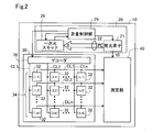
- FIG. 2 is a block diagram of an optical ranging device.
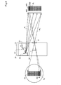
- FIG. 3 is an explanatory diagram showing the movement of the emitted beam and the reflected light in the optical ranging device.
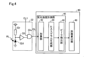
- FIG. 4 is an explanatory diagram showing the configuration of the measuring unit.
- FIG. 5 is an example of a histogram.
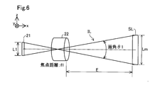
- FIG. 6 is a diagram showing an emission beam and its angle of view.
- FIG. 7 is a diagram showing an example of increasing the angle of view of the emission beam.
- FIG. 8 is a view of the light emitting element and the floodlight lens when viewed from the x direction.
- FIG. 9A is an explanatory diagram showing the second embodiment.
- FIG. 9B is an explanatory diagram showing a modified example of the second embodiment.
- FIG. 9C is an explanatory diagram showing a modified example of the second embodiment.
- FIG. 10 is an explanatory diagram showing an irradiated region and a non-irradiated region in the second embodiment.
- FIG. 11 is an explanatory diagram showing a third embodiment.
- FIG. 12 is an explanatory diagram showing a fourth embodiment.
- FIG. 13 is an explanatory diagram showing a fifth embodiment.
- FIG. 14 is an explanatory diagram showing a sixth embodiment.
- FIG. 15 is an explanatory diagram showing a seventh embodiment.
- FIG. 16 is a perspective view of the light emitting portion.
- FIG. 17 is a view of the light emitting portion including the projection lens when viewed from the z direction.
- FIG. 18A has a configuration in which a light refraction member is provided as a light guide path for narrowing the distance between the two emission beams.
- FIG. 18B has a configuration in which a reflector is provided as a light guide path for narrowing the distance between the two emission beams.
- FIG. 19 is a view of the floodlight lens as viewed from the x direction.
- FIG. 20 is an explanatory diagram showing a light emission control circuit of the light emitting element.
- FIG. 21 is an example showing the light receiving intensity of the reflected light when the deviation between the two emission beams is large.
- FIG. 22 is an example showing the light receiving intensity of the reflected light when the deviation between the two emission beams is small.
- FIG. 23 is an example showing the light receiving intensity of the reflected light when two light emitting beams are individually emitted.
- FIG. 24 is an explanatory diagram showing the configuration of the timing adjusting unit.
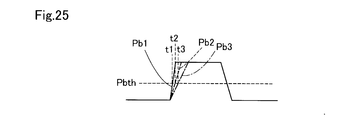
- FIG. 25 shows an example of adjusting the light emission timing of the light emitting element by adjusting the slew rate of the drive pulse.
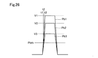
- FIG. 26 shows an example of adjusting the light emission timing of the light emitting element by adjusting the peak voltage of the drive pulse.
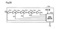
- FIG. 27 is an explanatory diagram showing a configuration example in which the timing adjusting unit has a delay circuit.
- FIG. 28 is an explanatory diagram showing a configuration example of the delay circuit.
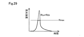
- FIG. 29 is an example showing a case where the maximum range of the light receiving intensity of the reflected light of the two emission beams is exceeded.
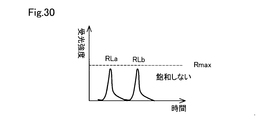
- FIG. 30 is an example showing the light receiving intensity of the reflected light when the emission timings of the two emission beams are shifted.
- the optical ranging device 10 is mounted on a vehicle, for example, and is used to measure the distance to an object. As shown in FIG. 1, the optical ranging device 10 includes a light emitting unit 20, a light receiving unit 30, and a measuring unit 40. The light emitting unit 20 emits a light emitting beam IL with respect to the measurement range MR. In the present embodiment, the light emitting unit 20 scans the light emitting beam IL in the scanning direction SD.
- the light emitting beam IL is formed in a rectangular shape whose longitudinal direction is orthogonal to the scanning direction SD.
- the light receiving unit 30 receives the reflected light RL from the range including the measurement range MR corresponding to the irradiation of the light emitting beam IL, and outputs a signal corresponding to the received state of the reflected light RL.
- the measuring unit 40 measures the distance to the object existing in the measurement range MR by using the signal output from the light receiving unit 30.
- the scanning direction may be any direction, and the scanning direction may be two-dimensional.
- FIG. 2 shows a block diagram of the optical ranging device 10.
- the light emitting unit 20 includes a light emitting element 21, a light projecting lens 22, a scanning control unit 29, and a one-dimensional scanner 26 which is a scanning device.
- the light emitting element 21 is composed of, for example, a semiconductor laser diode, and irradiates the one-dimensional scanner 26 with the pulsed laser light PL.
- the projectile lens 22 passes the pulsed laser light PL to generate an elongated rectangular light emitting beam IL.
- the one-dimensional scanner 26 reflects the emission beam IL and performs one-dimensional scanning in the SD direction of the measurement range MR.
- the one-dimensional scanner 26 has a mirror and a forced / resonant MEMS.
- the one-dimensional scanner 26 drives the forced / resonant MEMS to gradually rotate the angle of the mirror to change the direction of the light emitting beam IL and perform one-dimensional scanning in the SD direction.
- a reciprocating or rotating motion mirror may be used instead of the forced / resonant MEMS.
- the scanning control unit 29 detects the scanning angle of the one-dimensional scanner 26, and controls the emission of the pulsed laser light PL by the light emitting element 21 and the scanning of the emission beam IL using the one-dimensional scanner 26 based on the detection result. To do.
- the light receiving unit 30 includes a light receiving element array 34 and a decoder 36.
- the light receiving element array 34 is configured by arranging a plurality of light receiving elements 32 in a two-dimensional array of vertical n ⁇ horizontal m (n and m are natural numbers of 2 or more).
- the light receiving element 32 is composed of a single photon avalanche photodiode (SPAD), and the light receiving element array 34 is a SPAD array.
- the light receiving element 32 outputs a detection signal when light such as reflected light is incident on the light receiving surface. The configuration of the light receiving element 32 will be described later.
- the decoder 36 is a circuit for selecting the light receiving element 32.
- the decoder 36 includes selection control lines CL1 to CLn provided for each row of a matrix composed of a plurality of light receiving elements 32.
- the selection control lines CL1 to CLn are connected to each row in which the light receiving elements 32 arranged in the corresponding rows are divided into m units.
- the decoder 36 sequentially selects the light receiving elements 32 in column units by applying the selection control voltage to the selection control lines CL1 to CLn in order.
- the data of the light receiving element 32 selected in column units is output from the data lines DL1 provided in each row to DLm.
- the row directions correspond to the second direction described later, and the measuring unit 40 described later performs signal processing for each row along the second direction.
- the measuring unit 40 measures the distance to the object reflecting the light emitting beam IL based on the difference between the time t0 when the light emitting unit 21 irradiates the light emitting beam IL and the time when the light receiving unit 30 detects the reflected light RL. Perform processing.
- the measuring unit 40 is connected to DLm from the data lines DL1 provided for each row. Details of the configuration of the measuring unit 40 and data processing will be described later.
- FIG. 3 will be described until the pulsed laser light emitted from the light emitting element 21 reaches the light receiving unit 30.
- the pulsed laser light emitted from the light emitting element 21 having an elongated rectangular shape is magnified by the light projecting lens 22 to become a light emitting beam IL.
- the light emitting beam IL having a rectangular shape is reflected by the one-dimensional scanner 26 and directed toward an object (not shown).
- the reflected light RL diffusely reflected on the surface of the object is collected by the light receiving lens 31 and incident on the light receiving unit 30.
- the light receiving element 32 is composed of a well-known circuit including an avalanche photodiode 32d, a quenching resistor 32r, an inverter circuit 32i, and an AND circuit 32a. More specifically, in the light receiving element 32, the quenching resistor 32r and the avalanche photodiode 32d are connected in series between the power supply and the ground line, and the input side of the inverter circuit 32i is connected to the connection point. It is composed of. The quenching resistor 32r is connected to the power supply side, and the avalanche photodiode 32d is connected to the ground line side so as to have a reverse bias.
- the light receiving element 32 operates in the Geiger mode, and when the reflected light (one or more photons) reflected from the object is incident, it outputs a pulse signal indicating that the reflected light is incident with a certain probability.
- a pulse signal indicating that the reflected light is incident and a signal for selecting the selection control line CL1 are input to the AND circuit 32a. That is, the pulse signal obtained from the selection control line selected by the decoder 36, for example, the light receiving element 32 arranged in the row connected to the selection control line CL1, is output from the data line DL1 to DLm, for example.
- the measuring unit 40 includes a light receiving intensity measuring unit 45 and a distance calculating unit 48 for each of the data lines DL1 to DLm.
- the light receiving intensity measuring unit 45 includes an adding unit 42, a histogram generating unit 44, and a peak detecting unit 46.
- the addition unit 42 adds the number of pulse signals output to the data line DL1 substantially simultaneously from the plurality of light receiving elements 32 included in the light receiving unit 30 to obtain an addition value.
- the addition unit 42 outputs the obtained addition value to the histogram generation unit 44.
- the histogram generation unit 44 generates a histogram based on the added value output from the addition unit 42.
- FIG. 5 shows an example of a histogram.
- the class (horizontal axis) of the histogram indicates the flight time of light from the irradiation of light from the light emitting unit 21 to the reception of reflected light. This time is also called TOF (Time Of Flight).
- the frequency (vertical axis) of the histogram is an addition value calculated by the addition unit 42, and indicates the intensity of the reflected light RL reflected from the object.
- the histogram generation unit 44 generates a histogram by recording the addition value output from the addition unit 42 at predetermined time intervals according to the recording timing synchronized with the cycle of the emission beam emitted from the light emitting unit 21. .. If an object exists in the range irradiated by the light emitting unit 21, the frequency of the class corresponding to the time when the reflected light RL from the object is incident increases. That is, if there is a class having a large frequency in the histogram, the distance to the object can be calculated based on the time corresponding to the class. In generating one histogram, the frequency may be integrated by irradiating light a plurality of times. By doing so, the SN ratio can be improved.
- the peak detection unit 46 detects the peak from the histogram.
- the peak means a frequency exceeding a predetermined threshold value and a frequency at which the frequency becomes maximum.
- the distance calculation unit 48 calculates the distance to the object from the time corresponding to the peak.
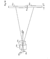
- the pulsed laser light emitted from the light emitting element 21 becomes a light emitting beam IL by the light emitting lens 22, and is magnified as an irradiation light SL at a position at a distance E from the light emitting lens 22.
- the length of the light emitting element 21 in the first direction is L1
- the focal length of the projection lens 22 is f1
- the length of the irradiation light SL in the first direction is Lm
- the angle of view of the light emitting beam IL is ⁇ 1.
- Lm L1 ⁇ E / f1 ...
- Lm 2 ⁇ E ⁇ tan ( ⁇ 1 / 2)... (2) Will be.
- the first direction is the longitudinal direction of the light emitting element 21, and in FIG. 6, it is the z direction.
- the figures attached to the present specification, including FIG. 6, are diagrams schematically shown for easy viewing, and the sizes and angles on the drawings do not represent accurate sizes and angles. Further, the illustration of the one-dimensional scanner 26 is omitted.
- the 7 and 8 are a method of doubling the angle of view of the emission beam in the present embodiment.
- two light emitting elements 21a and 21b and two floodlight lenses 22a and 22b are provided.
- Each of the two light emitting elements 21a and 21b has a length of L1 in the first direction (z direction), a length of D in the second direction (y direction) intersecting with the first direction, and L1>. It is D.
- the two light emitting elements 21a and 21b are arranged apart by a distance B in the second direction.
- the first light emitting lens 22a is provided corresponding to the first light emitting element 21a
- the second light emitting lens 22b is provided corresponding to the second light emitting element 21b.
- the first light emitting element 21a is located on the optical axis 22ao of the light projecting lens 22a
- the second light emitting element 21b is located on the optical axis 22bo of the light projecting lens 22b.
- the optical axes 22ao and 22bo are parallel to the x direction.
- the two projectile lenses 22a and 22b are arranged at positions that are separated from each other in the second direction and overlapped in the first direction. "Divided in the second direction" means that the two projectile lenses 22a and 22b do not overlap when the two projectile lenses 22a and 22b are viewed from the direction intersecting the second direction, for example, the x direction. Means to be visible.
- the "position overlapping with the first direction” means that when the two projectile lenses 22a and 22b are viewed from a direction intersecting the first direction, for example, a direction along the second direction, the two projectile lenses 22a and 22b It means that at least a part of the above appears to overlap.
- the focal lengths f2 of the two projection lenses 22a and 22b are both half the focal lengths f1 of the projection lens 22 of FIG.
- the light emitting beam ILa which is the light emitted from the light emitting element 21a
- the light emitting beam ILb which is the light emitted from the light emitting element 21b
- the width C is represented by the following equation (3).
- C D ⁇ E / f2...
- the first light emitting lens 22a is provided corresponding to the first light emitting element 21a
- the second light emitting lens 22b is provided corresponding to the second light emitting element 21b
- the first light emitting beam ILa is the first light emitting beam ILa.
- the second light emitting beam ILb does not pass through the first light emitting lens 22a without passing through the second light emitting lens 22b. Therefore, the two emission beams ILa and ILb are irradiated while maintaining a state of being shifted by B in the second direction, and the shift amount is not expanded at the irradiation destination and remains B. Then, among the widths C of the irradiation regions SLa and SLb, the range of the size of CB overlaps. In general, since E >> f2, C >> B. Therefore, the two emission beams ILa and ILb almost overlap each other, and can be regarded as substantially one emission beam.
- the length D of the first light emitting element 21a and the second light emitting element 21b in the second direction is 10 ⁇ m
- the focal length f1 is 5 mm
- the distance E to the irradiation destination is 100 m
- C is 0.2 m (200 mm). It becomes.
- the distance between the two light emitting elements 21a and 21b is 6 mm
- C + B is 206 mm
- the two light emitting beams ILa and ILb almost overlap each other and can be regarded as substantially one light emitting beam. ..
- the intensity of light per unit area in the overlapping portion of the two emission beams ILa and ILb is the same as the intensity of light per unit area in one emission beam IL of FIG.
- the reason for this is that the amount of light in the overlapped portion is doubled due to the overlap of the two emission beams ILa and ILb at the irradiation destination, but the length in the first direction is doubled, so that the amount of light per area is increased. This is because the light intensity is the same.
- the first light emitting element 21a and the second light emitting element 21a have a light emitting region longer than the length D in the second direction in which the length L1 of the light emitting region in the first direction intersects the first direction.
- the light emitting unit 21b is provided in the second direction so as to correspond to the light emitting unit 21, the first light emitting element 21a, and the second light emitting element 21b, which are arranged apart from each other by a predetermined distance B in the second direction. Since the two projection lenses 22a and 22b are provided at positions that are separated from each other and overlap each other in the first direction, the configuration shown in FIG. 6 does not reduce the intensity of light per unit area at the irradiation destination.
- the angle of view of the emission beams ILa and ILb can be increased to about twice as large as that of the above.
- the first light emitting element 21a is arranged so as to be slightly displaced in the first direction (z direction) with respect to the second light emitting element 21b. That is, the optical axes 22ao and 22bo of the two projection lenses 22a and 22b are parallel, and the first light emitting element 21a is on the side opposite to the first direction ( ⁇ z direction) from the optical axis 22ao of the corresponding projection lens 22a.
- the second light emitting element 21b is positioned so as to be shifted in the first direction from the optical axis 22bo of the corresponding light projecting lens 22b.
- the first light emitting element 21a each has four light emitting regions lda arranged in the first direction. Between the adjacent light emitting regions lda, three non-light emitting regions ldn that do not emit light are provided. That is, the four light emitting regions lda are arranged in the first direction with a non-light emitting region ldn opened between the adjacent light emitting regions lda. The non-light emitting region ldn is provided in order to increase the output of the light emitting elements 21a and 21b in each light emitting region lda.
- the second light emitting element 21b also includes a light emitting region ldb and a non-light emitting region ldn.
- the size of the non-light emitting region ldn in the first direction is smaller than the size of the light emitting region lda in the first direction, and in the first direction, the light emitting region lda of the first light emitting element becomes the non-light emitting region ldn of the second light emitting element.
- the first light emitting element and the second light emitting element are arranged so as to be positioned at overlapping positions so as to be shifted in the first direction.
- the first emission beam ILa forms four irradiation regions SLa1, SLa2, SLa3, and SLa4 in the first direction at the irradiation destination, and the non-irradiation due to the non-irradiation region ldn between them. Regions ga1, ga2, and ga3 are generated.
- the second emission beam ILb forms four irradiation regions SLb1, SLb2, SLb3, SLb4 in the first direction, and non-irradiation regions gb1, gb2, gb3 caused by the non-irradiation region ldn are formed between them. ing.
- the four irradiation regions SLa1, SLa2, SLa3, SLa4 and the four irradiation regions SLb1, SLb2, SLb3, SLb4 overlap in the second direction in the size range of CB of the enlarged width C. ing.
- the four irradiation regions SLa1, SLa2, SLa3, SLa4 and the four irradiation regions SLb1, SLb2, SLb3, SLb4 are also shifted in the first direction.
- the irradiation region SLb2 of the second emission beam ILb is located in the non-irradiation region ga1 between the irradiation regions SLa1 and SLa2, and similarly, the irradiation region SLb3 is located in the non-irradiation region ga2 and the non-irradiation region ga3.
- the irradiation region SLb4 is located at.
- the irradiation region SLa1 of the first emission beam ILa is located in the non-irradiation region gb1 between the irradiation regions SLb1 and SLb2, the irradiation region SLa2 is located in the non-irradiation region gb2, and the irradiation region SLa3 is located in the non-irradiation region gb3. positioned.
- the irradiation destination at least one of the first emission beam ILa and the second emission beam ILb is irradiated, so that there is no region where neither the first emission beam ILa nor the second emission beam ILb is irradiated. ..
- the first light emitting element 21a and the second light emitting element 21b each have four light emitting regions lda arranged in the first direction, but the first light emitting element 21a and the second light emitting element 21b Any configuration may be used as long as it has n light emitting regions lda (n is 2 or more) arranged in the first direction. Further, the number of light emitting regions lda of the first light emitting element 21a and the second light emitting element 21b may be the same, or may be different by one.
- the positions of the light receiving elements 32 corresponding to the non-irradiated regions ga1 to ga3 and gb1 to gb3 are known in advance. Therefore, even if the light receiving intensity of the reflected light RL in the light receiving element 32 corresponding to the non-irradiated regions ga1 to ga3 and gb1 to gb3 is small, the value of the histogram of the detection signal from the corresponding light receiving element 32 is doubled and normalized. By executing the above, it is possible to cope with the decrease in the light receiving intensity.
- the example shown in FIG. 9B is a modification of the example shown in FIG. 9A, in which the optical axes 22ao and 22bo of the two light emitting lenses 22a and 22b are parallel, and the first light emitting element 21a is the corresponding light emitting lens 22a.
- the second light emitting element 21b is located on the optical axis 22bo of the corresponding light projecting lens 22b, and the two optical axes 22ao and 22bo are positioned shifted in the first direction. .. Even with this configuration, the same effect as that of the second embodiment shown in FIG. 9A can be obtained.
- the first light emitting element 21a is located on the optical axis 22ao of the corresponding light emitting lens 22a
- the second light emitting element 21b is located on the optical axis 22bo of the corresponding light emitting lens 22b.
- the optical axes 22ao and 22bo are inclined in the first direction and in directions opposite to the first direction, respectively. Even with this configuration, the same effect as that of the second embodiment shown in FIG. 9A can be obtained.
- a cylindrical lens 27 is provided after the two projection lenses 22a and 22b.
- the cylindrical lens 27 has a function of doubling the angle of view of the emission beams ILa and ILb in the first direction.
- the cylindrical lens 27 does not enlarge the angle of view in the second direction.
- the angles of view of the first emission beam ILa and the second emission beam ILb are magnified by using the cylindrical lens 27 to twice the angle of view when the cylindrical lens 27 is not used, and thus two projection lenses. Even if a projection lens having the same focal length as the focal length f1 of the projection lens 22 of FIG. 6 is used as the 22a and 22b, the angle of view can be doubled. Further, the intensity of light per unit area in the overlapping portion of the two emission beams ILa and ILb can be made the same as the intensity of light per unit area in one emission beam IL of FIG.
- the cylindrical lens 27 does not expand the angle of view in the second direction, if the cylindrical lens 27 is used, the widths of the emission beams ILa and ILb in the second direction are not expanded, so that the resolution of detection in the second direction can be increased.
- the angle of view in the first direction can be enlarged without lowering it.
- the first light emission is such that the first region SLa irradiated by the first light emitting element 21a and the second region SLb irradiated by the second light emitting element 21b are in contact with each other in the first direction.
- the element 21a and the second light emitting element 21b are arranged. That is, the first light emitting element 21a is located on the optical axis 22ao of the corresponding light emitting lens 22a, the second light emitting element 21b is located on the optical axis 22bo of the corresponding light emitting lens 22b, and the two optical axes 22ao,
- the 22bo is tilted in each of the first direction and the direction opposite to the first direction.
- the first emission beam ILa irradiates the region corresponding to the upper angle of view ⁇ 1 in FIG. 12, and the second emission beam ILb illuminates the region corresponding to the lower angle of view ⁇ 1 in FIG.
- Both the first emission beam ILa and the second emission beam ILb irradiate the region corresponding to the angle of view 2 ⁇ 1.
- the light intensities of the first region SLa and the second region SLb are the same as the light intensities in FIG.
- the angles of view of the light emitting beams ILa and ILb are doubled, and the intensity of light per unit area at the irradiation destination is determined by the unit area of one light emitting beam IL of FIG. It can be the same as the intensity of light.
- the first region SLa and the second region SLb are only shifted by B in the second direction, and are in contact with each other by the length of CB. Since C >> B, the first region SLa and the second region SLb can be regarded as substantially one. Since C >> B, it can be regarded as substantially one emission beam at the irradiation destination. Further, according to the fourth embodiment, since the centers of the two light projecting lenses 22a and 22b are arranged at the same position with respect to the first direction, there is no undetectable place.
- a cylindrical lens 27 is provided after the two projectile lenses 22a and 22b, and the focal length of the projectile lenses 22a and 22b is 2f1 which is twice that of the example shown in FIG. ..
- the angles of view of the emission beams ILa and ILb are doubled, and the intensity of light per unit area at the irradiation destination is determined by one emission beam of FIG. It can be the same as the intensity of light per unit area in IL. Further, since the cylindrical lens 27 does not enlarge the angle of view in the second direction, the angle of view in the first direction can be enlarged without deteriorating the accuracy in the second direction as in the third embodiment.
- the first region SLa and the second region SLb are only shifted by B in the second direction, and have a length of CB. I'm in contact. Since C >> B, the first region SLa and the second region SLb can be regarded as substantially one. Further, even when the first light emitting element 21a and the second light emitting element 21b have a non-light emitting region, the four irradiation regions SLa1, SLa2, SLa3, and SLa4 expand in the first direction, so that the non-light emitting region is formed. The resulting non-irradiated regions ga1, ga2, and ga3 can be eliminated.
- the sixth embodiment shown in FIG. 14 is substantially the same as the fourth embodiment shown in FIG. 12, but differs in the following points.
- the central axis 22ao of the first floodlight lens 22a and the central axis 22bo of the second floodlight lens 22b are not parallel and spread in the first direction at the irradiation destination.
- the central axis 22ao of the first floodlight lens 22a and the central axis 22bo of the second floodlight lens 22b are parallel to each other.
- the first light emitting element 21a is positioned shifted from the optical axis 22ao of the corresponding light emitting lens 22a in the direction opposite to the first direction ( ⁇ z direction), and the second light emitting element 21b is located on the corresponding light emitting lens 22b. It is positioned shifted from the optical axis 22b0 in the first direction (z direction).
- the first emission beam ILa is not parallel to the central axis 22ao of the first projection lens 22a
- the second emission beam ILb is not parallel to the central axis 22bo of the second projection lens 22b.
- the angles of view of the emission beams ILa and ILb are doubled, and the intensity of light per unit area at the irradiation destination is determined by one emission beam of FIG. It can be the same as the intensity of light per unit area in IL. Further, since C >> B, it can be regarded as substantially one emission beam at the irradiation destination.
- the seventh embodiment shown in FIG. 15 is substantially the same as the fifth embodiment shown in FIG. 13, but similarly to the sixth embodiment with respect to the fourth embodiment, the central axis 22ao of the first floodlight lens 22a and The central axis 22bo of the second light emitting lens 22b is parallel to the central axis 22bo of the first light emitting lens 22a, and the positions of the light emitting elements 21a and 21b in the first direction are shifted. Instead, the second emission beam ILb is not parallel to the central axis 22bo of the second projection lens 22b.
- the angles of view of the emission beams ILa and ILb are doubled, and the intensity of light per unit area at the irradiation destination is determined by one emission beam of FIG. It can be the same as the intensity of light per unit area in IL. Further, since C >> B, it can be regarded as substantially one emission beam at the irradiation destination.
- FIG. 16 is a perspective view
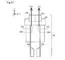
- FIG. 17 is a view of the light emitting unit 20 including the projection lens 22a22b from the z direction. As described above, the configurations shown in FIGS. 16 and 17 are applicable to the first to seventh embodiments.
- the first light emitting element 21a is installed on one surface 23a1 of the first substrate 23a
- the second light emitting element 21b is installed on one surface 23b1 of the second substrate 23b.
- the surfaces 23a1 and 23b1 face each other.
- the light emitting beams ILa and ILb emitted from the first light emitting element 21a and the second light emitting element 21b pass through the light projecting lenses 22a and 22b, respectively, and are irradiated in the x direction.
- a lens barrel 22t is provided on the outer edge of the projectile lenses 22a and 22b.
- the lens barrel 22t also covers the circumference of the first light emitting element 21a on the first substrate 23a and the second light emitting element 21b on the second substrate 23b.
- the surface 23a1 on which the first light emitting element 21a is arranged and the surface 23b1 on which the second light emitting element 21b is arranged face each other, so that the first light emitting element 21a and the second light emitting element 21b The interval B between them can be reduced. As a result, the ratio of the emission beams ILa and ILb overlapping at the irradiation destination can be increased.
- the first light emitting element 21a and the second light emitting element 21b are arranged on the opposing surfaces 23a1 and 23b1, the back surfaces of the surfaces 23a1 and 23b1, that is, the surfaces 23a2 and 23b2 are like heat dissipation plates.
- a heat dissipation structure can be attached. As a result, the heat generated in the first light emitting element 21a and the second light emitting element 21b can be easily dissipated.
- FIGS. 18A and 18B includes a light guide path that narrows the distance between the light emitting beams ILa and ILb. As described above, these configurations are also applicable in the first to seventh embodiments.
- the configuration shown in FIG. 18A includes light refraction members 24a and 24b after the light projecting lenses 22a and 22b.
- the light refracting members 24a and 24b function as a light guide path, refract the light emitting beams ILa and ILb, and further narrow the distance between them. As a result, the ratio of the emission beams ILa and ILb overlapping at the irradiation destination can be increased.
- the configuration shown in FIG. 18B includes light reflecting members 24c, 24d, and 24e in the rear stage of the floodlight lenses 22a and 22b.
- the light reflecting members 24c, 24d, and 24e also function as light guide paths, and by reflecting the light emitting beams ILa and ILb, the intervals thereof are further narrowed. As a result, the ratio of the emission beams ILa and ILb overlapping at the irradiation destination can be increased.
- FIG. 19 is a view of the floodlight lenses 22a and 22b according to the first to seventh embodiments as viewed from the x direction.
- the two light projecting lenses 22a and 22b have flat portions 22af and 22bf on their outer edges, respectively, and a lens barrel 22t is provided on the outer edges of the flat portions 22af and 22bf, respectively.
- a light-shielding wall 22s is provided between the two projection lenses 22a and 22b. The z-direction of the light-shielding wall 22s is in contact with the lens barrel 22t.
- the light emitting beams ILa and ILb of the two projectile lenses 22a and 22b are surrounded by the lens barrel 22t or the light shielding wall 22s, the light emitting beams ILa and ILb are not mixed.
- the effective lens diameter means a region where the angle of view of the emission beams ILa and ILb can be enlarged.
- the second direction (y direction) does not participate in the expansion of the angle of view of the emission beams ILa and ILb by the projectile lenses 22a and 22b in the first direction (z direction)
- the center of the first projectile lens 22a since the second direction (y direction) does not participate in the expansion of the angle of view of the emission beams ILa and ILb by the projectile lenses 22a and 22b in the first direction (z direction), the center of the first projectile lens 22a.
- the distance between the shaft 22ao and the central shaft 22bo of the second projection lens 22b may be ea or narrower than ea.
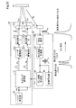
- the control of the first light emitting element 21a and the second light emitting element 21b in each of the above embodiments will be described with reference to FIG. As described above, the light emission control described with reference to FIGS. 20 and 20 can be applied to any of the first to seventh embodiments.
- the light emitting unit 20 includes a pulse generating unit 50, a timing adjusting unit 51, and laser driving units 52a and 52b.
- the light receiving unit 30 includes a light receiving element 32, a light receiving intensity measuring unit 45, a distance calculating unit 48, and a deviation time measuring unit 49.
- the pulse generation unit 50 generates the drive pulse P0.
- the drive pulse P0 is input to the timing adjusting unit 51, which is an adjusting mechanism for adjusting the light emitting timings of the two light emitting elements 21a and 21b.
- the timing adjustment unit 51 adjusts the timing of the pulse P0 and generates the drive pulses Pa and Pb. A configuration example of the timing adjusting unit 51 will be described later.
- the first laser driving unit 52a receives the input of the driving pulse Pa and drives the first light emitting element 21a to cause the first light emitting element 21a to emit the light emitting beam ILa.
- the second laser driving unit 52b receives the input of the driving pulse Pb, drives the second light emitting element 21b, and causes the second light emitting element 21b to emit the light emitting beam ILb.
- the reflected light RLa and RLb are received by the light receiving unit 30.
- the light receiving intensity measuring unit 45 measures the light receiving intensity in the light receiving unit 30.
- the light receiving intensity measuring unit 45 measures the light receiving intensity by using, for example, the result of the histogram generation unit 44 when the reflected light RL from an object arranged at a predetermined distance is received. If there is a large difference in the light emission timing between the first light emitting element 21a and the second light emitting element 21b, the output signal of the light receiving intensity measuring unit 45 has two peaks as shown in FIG. If the light emitting timings of the first light emitting element 21a and the second light emitting element 21b match, one peak is obtained as shown in the graph above FIG.
- the deviation time measuring unit 49 calculates a correction amount ⁇ t for matching the light emitting timings of the first light emitting element 21a and the second light emitting element 21b using these waveforms, and the timing adjusting unit 51 calculates the calculated correction amount.
- Send ⁇ t the timing adjusting unit 51 may perform timing adjustment at the time of shipping inspection of the optical ranging device 10, and even after shipping and mounting on the vehicle, during periodic inspection of the vehicle or during operation of this device. You may go intermittently.
- the timing adjusting unit 51 may be performed while the vehicle is not traveling. When the four irradiation regions of each laser are output by different drive pulses, the four timing deviations may be measured and corrected individually.
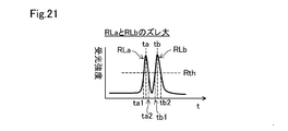
- FIG. 21 shows the reflected light RLa and RLb when there is a large deviation between the emission beams ILa and ILb.
- the graph showing the reflected light RLa and RLb corresponds to a smooth curve of the histogram shown in FIG. 4B.
- the received waveforms of the reflected light RLa and RLb show two peaks, a peak caused by the emission beam ILa and a peak caused by the emission beam ILb.
- the shift time measuring unit 49 directly obtains these two peak positions, that is, the time ta at which the reflected light RLa of the light emitting beam ILa peaks and the time tb at which the reflected light RLb of the light emitting beam ILb peaks. Is also good. Further, the time ta1 in which the reflected light RLa of the light emitting beam ILa exceeds the threshold value Rth and the time ta2 in which the reflected light RLa of the light emitting beam ILa cuts the threshold value Rth are obtained, and the intermediate time (ta1 + ta2) / 2 is set in the light emitting beam ILa. The time ta at which the reflected light RLa peaks may be set.
- the time tb at which the reflected light RLb of the light emitting beam ILb peaks may be obtained.
- the time ta and tb can be easily obtained.
- FIG. 22 shows a case where the deviation between the emission beams ILa and ILb is small.
- the timings of the emission beams ILa and ILb match, the timings of the reflected lights RLa and RLb almost match as in the ideal waveform, the reflected lights RLa and RLb become one peak, and the peak becomes the threshold value Rth.
- the pulse width ⁇ t1 which is the time exceeding the above, is the shortest, and the peak value Rp1 is the highest.
- the timings of the emission beams ILa and ILb are slightly different, the two emission beams ILa and ILb overlap to form a broad waveform.
- the pulse width ⁇ t2 which is the time when the threshold value Rth is exceeded, becomes longer, and the peak value Rp2 becomes lower.
- the larger the deviation amount the larger the pulse width ⁇ t2 and the lower the peak value Lp2. Therefore, the deviation time measuring unit 49 can determine how much the emission beam ILa and ILb are displaced by measuring the pulse width ⁇ t2 and comparing it with the pulse width ⁇ t1 of the ideal waveform measured in advance. .. At this time, the deviation time measuring unit 49 may consider how much the peak value Rp2 is lower than the peak value Rp1.
- the deviation time measuring unit 49 repeatedly changes the correction amount ⁇ t little by little and outputs it, and measures the time ⁇ t2 when the two emission beams ILa and ILb exceed the threshold value Rth when the correction amount ⁇ t is output.
- the correction amount ⁇ t at which the time ⁇ t2 at which the two reflected lights RLa and RLb exceed the threshold value Lth is the shortest may be determined.
- the shift time measuring unit 49 has a time tpa at which the reflected light RLa peaks when only the first laser driving unit 52a is driven to emit light only the first light emitting element 21a, and a second The time tpb at which the reflected light RLb peaks when only the second light emitting element 21b is driven by driving only the laser driving unit 52b may be acquired, and the difference ⁇ t may be used as the correction amount.
- the time tapa and tpb can be obtained by the same method as in FIG.
- the timing adjusting unit 51 includes two inverters 51i1 and 51i2, a digital analog converter 51a (hereinafter referred to as “DAC51a”), and an amplifier 51b.
- the inverters 51i1 and 51i2 generate a drive pulse Pb in which the drive pulse P0 is delayed.
- the DAC 51a converts the correction value ⁇ t, which is a digital value calculated by the deviation time measuring unit 49, into an analog voltage Vin.
- the amplifier 51b has a level shifter or a variable resistor, and generates a drive pulse Pb in which the drive pulse P0 is delayed based on the analog voltage Vin.
- the amplifier 51b adjusts the rising slew rate of the drive pulse Pb based on the input voltage Vin. For example, when Vin is large (Vin1), the amplifier 51b raises the drive pulse Pb1 at a short slew rate. In this case, the input threshold value Pbth of the second laser driving unit 52b is exceeded at time t1. When the magnitude of the pulse Pb1 exceeds the input threshold value Pbth, power is supplied to the light emitting element 21b, and the light emitting element 21b emits light. When Vin2 is smaller than Vin1, the amplifier 51b raises the drive pulse Pb at a slew rate longer than the drive pulse Pb1 like Pb2.
- the input threshold value Pbth of the second laser driving unit 52b is exceeded at time t2.
- Time t2 is later than time t1.
- Vin3 is smaller than Vin2
- the input threshold value Pbth of the second laser drive unit 52b is exceeded at time t3 later than time t2, power is supplied to the light emitting element 21b, and the light emitting element 21b emits light.
- the amplifier 51b adjusts the rising slew rate of the drive pulse Pb based on the input voltage Vin.
- the delay amounts of the two inverters 51i1 and 51i2 are set so that the first light emitting element 21a and the second light emitting element 21b emit light at almost the same time when Vin is Vin2, when Vin is Vin1
- the light emission timing of the second light emitting element 21b can be earlier than the light emission timing of the first light emitting element 21a, and when Vin is Vin 3, the light emission timing of the second light emitting element 21bb can be delayed from the light emission timing of the first light emitting element 21a.
- the amplifier 51b adjusts the slew rate of the drive pulse Pb, but in the example shown in FIG. 26, the amplifier 51b peaks the drive pulse Pb based on the input voltage Vin. Adjust the voltage. For example, when Vin is large (Vin1), the amplifier 51b sets the peak voltage of the drive pulse Pb1 to V1. In this case, the input threshold value Pbth of the second laser driving unit 52b is exceeded at time t1. Similarly, when Vin is smaller than Vin1, the drive pulse Pb2 exceeds the input threshold Pbth at time t2 later than time t1, and when Vin is Vin3 smaller than Vin2, the drive pulse Pb3 is , The input threshold value Pbth is exceeded at time t3, which is later than time t2. In this way, the amplifier 51b can adjust the light emission timing of the light emitting element 21b by adjusting the peak voltage of the drive pulse Pb based on the input voltage Vin.
- the timing adjusting unit 51 adjusts the timing of the drive pulse Pb, but the timing of the drive pulse Pa and the timing of both the drive pulse Pa and Pb may be adjusted.
- the examples shown in FIGS. 25 and 26 are examples of changing the waveform (slew rate or peak voltage) of the drive pulse Pb, but the example shown in FIG. 27 is an example in which the timing adjusting unit 51 includes a delay circuit.
- the timing adjusting unit 51 includes a first delay circuit 53a that delays the drive pulse P0 to generate the drive pulse Pa, and a second delay circuit 53b that delays the drive pulse P0 to generate the drive pulse Pb.
- the first delay circuit 53a includes an even number of inverter INVs connected in series and a delay selection unit 53as.
- the output of the drive pulse Pa and the even-numbered inverter INV is input to the delay selection unit 53as, and one of them is selected according to the correction amount and output as the drive pulse Pa.
- the first delay circuit 53a outputs the drive pulse Pa in which the drive pulse P0 is delayed in this way.
- the delay selection unit 53as selects the drive pulse P0, the drive pulse Pa coincides with the drive pulse P0 and outputs a drive pulse Pa that is not substantially delayed.
- the second delay circuit 53b is the same circuit, and the drive pulse P0 is delayed to generate the drive pulse Pb.
- the first delay circuit 53a has a configuration in which only an even number, for example, two inverter INVs are provided without the delay selection unit 53as. You may.
- the delay selection unit 53as selects the drive pulse P0, the drive pulse Pa can be delayed with respect to the drive pulse Pb.
- the delay selection unit 53as selects the output P1 of the second-stage inverter, the drive pulse Pa and the drive pulse Pb can be set at almost the same timing, and the delay selection unit 53as can select the output P2 of the fourth-stage inverter.
- the drive pulse Pb can be delayed with respect to the drive pulse Pa.
- the timing adjusting unit 51 can adjust the light emitting timing of the light emitting elements 21a and 21b regardless of which of the light emitting elements 21a and 21b is earlier.
- FIG. 29 shows a case where the light emitting beams ILa and ILb are irradiated to a substance having high reflectance, and the light receiving unit 30 receives the reflected light RL.
- the light receiving intensity exceeds the maximum range Rmax of the light receiving unit 30.
- the portion where the light receiving intensity exceeds Rmax becomes broad, the light receiving intensity measuring unit 45 cannot accurately cut off the peaks of the reflected light RLa and RLb, and the distance calculating unit 48 is a substance having high reflectance. It can be difficult to accurately measure the distance to.
- the measuring unit 40 uses the light receiving intensity of the reflected light RLa and RLb in the light receiving unit 30 to intentionally notify the timing adjusting unit 51 of the light emitting timing of the first light emitting element 21a and the second light emitting element 21b.
- the light emission timing may be adjusted so as to be different.
- the light receiving intensity of the reflected light RLa of the light emitting beam ILa does not exceed the maximum range Rmax of the light receiving unit 30, and the light receiving intensity of the reflected light RLb of the light emitting beam ILb is the maximum range Rmax of the light receiving unit 30. Do not exceed.
- the light receiving intensity measuring unit 45 correctly determines each peak of the reflected light RLa and RLb, and the distance calculating unit 48 can measure the distance to the substance having high reflectance. Since the emission timing of the emission beam ILa and the adjustment amount of the emission timing of the emission beam ILb performed by the timing adjustment unit 51 are known in advance, the distance calculation unit 48 can easily correct the emission timing.
- the emission timing of the emission beam ILa and the emission timing of the emission beam ILb may be the same, and FIGS. As explained in the above, the timing may be intentionally different.
- the present disclosure is not limited to the above-described embodiment, and can be realized by various configurations within a range not deviating from the purpose.
- the technical features of the embodiments corresponding to the technical features in each embodiment described in the column of the outline of the invention are for solving a part or all of the above-mentioned problems, or a part of the above-mentioned effects. Or, in order to achieve all of them, it is possible to replace or combine them as appropriate. Further, if the technical feature is not described as essential in the present specification, it can be appropriately deleted.
Landscapes
- Engineering & Computer Science (AREA)
- Physics & Mathematics (AREA)
- General Physics & Mathematics (AREA)
- Radar, Positioning & Navigation (AREA)
- Remote Sensing (AREA)
- Computer Networks & Wireless Communication (AREA)
- Electromagnetism (AREA)
- Optical Radar Systems And Details Thereof (AREA)
- Measurement Of Optical Distance (AREA)
Abstract
光を用いた光学的測距装置(10)は、発光領域の第1方向の長さが前記第1方向に交差する第2方向に比べて長い発光領域を有する第1発光素子(21a)と第2発光素子(21b)とを、前記第2方向に予め定められた距離だけ離間して配置した発光部(20)と、前記第1発光素子、前記第2発光素子にそれぞれ対応して設けられ、前記第2方向に隔たり、かつ、前記第1方向に重なる位置に配置された2個の投光レンズ(22a、22b)と、前記発光部から射出され、2個の前記投光レンズを通過した発光ビームを測定範囲に向けて走査させるスキャナ(26)と、前記発光部から射出された前記発光ビームの反射光を受光する受光部(30)と、前記発光部の発光から前記受光部での受光までの時間に応じて対象物までの距離を測定する測定部(40)と、を備える。
Description
本願は、2019年6月19日に出願された出願番号2019-113847号の日本出願に基づく優先権を主張し、その開示の全てが参照により本願に組み込まれる。
本開示は、光学的測距装置に関する。
前方の対象物を検出する装置として、光を用いて検出する光学的測距装置が開発されている(例えば特許文献1)。この装置は、鉛直方向に細長い帯状のビームを、水平方向(ビームの短辺方向)に走査する。鉛直方向の光照射範囲は、ビームの長辺方向の長さと投光レンズの倍率で決められている。
近年、光照射範囲、特に鉛直方向の光照射範囲を大きくして、対象物の検出範囲を大きくすることが求められている。そこで、簡単な構成で鉛直方向の光照射範囲を大きくする構成が求められていた。
本開示の一形態によれば、光を用いた光学的測距装置が提供される。光学的測距装置は、発光領域の第1方向の長さが前記第1方向に交差する第2方向に比べて長い発光領域を有する第1発光素子と第2発光素子とを、前記第2方向に予め定められた距離だけ離間して配置した発光部と、前記第1発光素子、前記第2発光素子にそれぞれ対応して設けられ、前記第2方向に隔たり、かつ、前記第1方向に重なる位置に配置された2個の投光レンズと、前記発光部から射出され、2個の前記投光レンズを通過した発光ビームを測定範囲に向けて走査させるスキャナと、前記発光部から射出された前記発光ビームの反射光を受光する受光部と、前記発光部の発光から前記受光部での受光までの時間に応じて対象物までの距離を測定する測定部と、を備える。この形態によれば、発光ビームの照射先における光の強度を維持したまま発光ビームの画角を大きくできる。
・第1実施形形態:
光学的測距装置10は、例えば車両に搭載され、対象物までの距離を測定するために用いられる。図1に示すように、光学的測距装置10は、発光部20と、受光部30と、測定部40と、を備える。発光部20は、測定範囲MRに対して発光ビームILを射出する。本実施形態では、発光部20は、発光ビームILを走査方向SDに走査する。発光ビームILは、走査方向SDに直交する方向が長手方向となる矩形形状に形成されている。受光部30は、発光ビームILの照射に応じた測定範囲MRを含む範囲からの反射光RLを受光し、反射光RLの受光状態に応じた信号を出力する。測定部40は、受光部30から出力された信号を用いて、測定範囲MR内に存在する対象物までの距離を測定する。なお、走査方向は、いずれの方向でもよく、2次元的に走査してもよい。
光学的測距装置10は、例えば車両に搭載され、対象物までの距離を測定するために用いられる。図1に示すように、光学的測距装置10は、発光部20と、受光部30と、測定部40と、を備える。発光部20は、測定範囲MRに対して発光ビームILを射出する。本実施形態では、発光部20は、発光ビームILを走査方向SDに走査する。発光ビームILは、走査方向SDに直交する方向が長手方向となる矩形形状に形成されている。受光部30は、発光ビームILの照射に応じた測定範囲MRを含む範囲からの反射光RLを受光し、反射光RLの受光状態に応じた信号を出力する。測定部40は、受光部30から出力された信号を用いて、測定範囲MR内に存在する対象物までの距離を測定する。なお、走査方向は、いずれの方向でもよく、2次元的に走査してもよい。
図2に光学的測距装置10のブロック図を示す。発光部20は、発光素子21と、投光レンズ22と、走査制御部29と、スキャン装置である一次元のスキャナ26と、を備える。発光素子21は、例えば半導体レーザダイオードで構成されており、パルスレーザ光PLを一次元スキャナ26に照射する。投光レンズ22は、パルスレーザ光PLを通過させて細長い矩形形状の発光ビームILを生成する。
一次元スキャナ26は、発光ビームILを反射して測定範囲MRのSD方向の一次元の走査を行う。一次元スキャナ26は、ミラーと、強制・共振型MEMSと、を有している。一次元スキャナ26は、強制・共振型MEMSを駆動することにより、ミラーの角度を少しずつ回転させることで、発光ビームILの方向を変え、SD方向への一次元の走査を行う。強制・共振型MEMSの代わりに、往復または回転運動型ミラーを用いても良い。
走査制御部29は、一次元スキャナ26の走査角度を検出し、この検出結果に基づいて、発光素子21によるパルスレーザ光PLの発光と、一次元スキャナ26を用いた発光ビームILの走査を制御する。
受光部30は、受光素子アレイ34とデコーダ36とを備える。受光素子アレイ34は、複数の受光素子32を縦n×横m(n、mは、2以上の自然数)の二次元のアレイ状に配列することで構成されている。受光素子32は、シングルフォトンアバランシフォトダイオード(SPAD)で構成されており、受光素子アレイ34は、SPADアレイである。受光素子32は、その受光面に反射光等の光が入射すると、検出信号を出力する。受光素子32の構成については、後述する。
デコーダ36は、受光素子32を選択するための回路である。デコーダ36は、複数の受光素子32により構成される行列の列毎に設けられた選択制御線CL1からCLnを備える。選択制御線CL1からCLnは、対応する列に配置されている受光素子32をm個ずつに分けた列毎に接続される。デコーダ36は、選択制御線CL1からCLnに順に選択制御電圧を印加することにより、列単位で受光素子32を順に選択する。列単位で選択された受光素子32のデータは、それぞれの行に設けられたデータ線DL1からDLmに出力される。行の方向は、後述する第2方向に対応しており、後述する測定部40では、第2方向に沿った行毎に信号処理が行われる。
測定部40は、発光部21が発光ビームILを照射した時刻t0と、受光部30が反射光RLを検出した時刻との差に基づいて、発光ビームILを反射した物体までの距離を計測する処理を行う。測定部40は、行毎に設けられているデータ線DL1からDLmに接続されている。測定部40の構成とデータ処理についての詳細は後述する。
図3を用いて、発光素子21から発光されたパルスレーザ光が受光部30に到達するまでを説明する。細長い矩形形状を有する発光素子21から発光されたパルスレーザ光は、投光レンズ22により拡大されて発光ビームILになる。矩形形状を有する発光ビームILは、一次元スキャナ26で反射して物体(図示せず)に向かう。物体の表面で乱反射した反射光RLは、受光レンズ31により集光されて、受光部30に入射する。
図4に示すように、受光素子32は、アバランシェフォトダイオード32dと、クエンチング抵抗器32rと、インバータ回路32iと、AND回路32aを含む周知の回路によって構成されている。より具体的には、受光素子32は、電源と接地ラインとの間に直列にクエンチング抵抗器32rとアバランシェフォトダイオード32dとが接続され、その接続点にインバータ回路32iの入力側が接続されることにより構成されている。クエンチング抵抗器32rは電源側に接続され、アバランシェフォトダイオード32dは、逆バイアスとなるように接地ライン側に接続されている。受光素子32は、ガイガーモードで動作し、物体から反射された反射光(1つ以上のフォトン)が入射されると、その反射光が入射したことを示すパルス信号を一定の確率で出力する。AND回路32aには、反射光が入射したことを示すパルス信号と、選択制御線CL1を選択する信号とが入力されている。すなわち、デコーダ36で選択された選択制御線、例えば選択制御線CL1に接続された列に配置されている受光素子32から得られるパルス信号を、例えばデータ線DL1からDLmに出力する。
測定部40は、データ線DL1からDLmのそれぞれに、受光強度計測部45と、距離算出部48と、を備える。受光強度計測部45は、加算部42と、ヒストグラム生成部44と、ピーク検出部46とを備える。
加算部42は、受光部30に含まれる複数の受光素子32から略同時にデータ線DL1に出力されたパルス信号の数を加算して加算値を求める。加算部42は、求めた加算値をヒストグラム生成部44に出力する。
ヒストグラム生成部44は、加算部42から出力された加算値に基づきヒストグラムを生成する。図5は、ヒストグラムの一例を示している。ヒストグラムの階級(横軸)は、発光部21から光が照射されてから反射光が受光されるまでの光の飛行時間を示している。この時間のことを、TOF(Time Of Flight)ともいう。ヒストグラムの度数(縦軸)は、加算部42によって算出された加算値であり、物体から反射してきた反射光RLの強度を示している。ヒストグラム生成部44は、発光部21から照射される発光ビームの周期に同期した記録タイミングに従って、加算部42から出力された加算値を予め定められた時間間隔ごとに記録することによってヒストグラムを生成する。発光部21によって光が照射される範囲に物体が存在すれば、その物体からの反射光RLが入射する時刻に対応する階級の度数が大きくなる。つまり、ヒストグラムにおいて大きな度数を有する階級が存在すれば、その階級に対応する時刻に基づいて、物体までの距離を算出することができる。なお、1つのヒストグラムを生成するにあたり、光を複数回照射して度数を積算してもよい。こうすることにより、SN比を向上させることができる。
ピーク検出部46は、ヒストグラムからピークを検出する。本実施形態において、ピークとは、予め定めた閾値を超える度数であり、かつ、度数が極大となる度数を意味する。距離算出部48は、ピークに対応する時刻から、物体までの距離を算出する。
図6に示すように、発光素子21から射出されたパルスレーザ光は、投光レンズ22により発光ビームILとなり、投光レンズ22から距離Eの位置で照射光SLとして拡大される。ここで、発光素子21の第1方向の長さをL1、投光レンズ22の焦点距離をf1、照射光SLの第1方向の長さをLm、発光ビームILの画角をθ1とすると、
Lm=L1×E/f1 …(1)
Lm=2×E×tan(θ1/2) …(2)
となる。ここで、第1方向とは、発光素子21の長手方向であり、図6では、z方向である。なお、図6を含め、本明細書に添付する図は、見やすくするために模式的に示した図であり、図面上のサイズや角度は、正確なサイズ、角度を表していない。また、一次元スキャナ26の図示を省略している。
Lm=L1×E/f1 …(1)
Lm=2×E×tan(θ1/2) …(2)
となる。ここで、第1方向とは、発光素子21の長手方向であり、図6では、z方向である。なお、図6を含め、本明細書に添付する図は、見やすくするために模式的に示した図であり、図面上のサイズや角度は、正確なサイズ、角度を表していない。また、一次元スキャナ26の図示を省略している。
図7、図8は、本実施形態における発光ビームの画角を2倍にする方法である。本実施形態では、2個の発光素子21a、21bと、2個の投光レンズ22a、22bを備えている。2個の発光素子21a、21bは、いずれも第1方向(z方向)の長さがL1であり、第1方向と交差する第2方向(y方向)の長さがDであり、L1>Dである。2個の発光素子21a、21bは、第2方向に間隔Bだけ離間して配置されている。第1投光レンズ22aは、第1発光素子21aに対応して設けられ、第2投光レンズ22bは、第2発光素子21bに対応して設けられている。第1発光素子21aは、投光レンズ22aの光軸22ao上に位置し、第2発光素子21bは、投光レンズ22bの光軸22bo上に位置している。光軸22ao、22boはx方向に平行である。2つの投光レンズ22a、22bは、第2方向に隔たり、かつ、第1方向に重なる位置に配置されている。「第2方向に隔たる」とは、第2方向と交わる方向、例えばx方向から2つの投光レンズ22a、22bを見た時に、2個の投光レンズ22a、22bが重なっていないように見えることを意味する。「第1方向に重なる位置」とは、第1方向と交わる方向、例えば第2方向に沿った方向から2個の投光レンズ22a、22bを見た時に、2個の投光レンズ22a、22bの少なくとも一部同士が重なっているように見えることを意味する。2個の投光レンズ22a、22bの焦点距離f2は、いずれも図6の投光レンズ22の焦点距離f1の半分である。
本実施形態では、発光素子21aから射出された光である発光ビームILaと、発光素子21bから射出された光である発光ビームILbは、照射先において、照射領域SLa、SLbの第2方向の幅がCに拡大されている。幅Cは、以下の式(3)で表される。
C=D×E/f2 …(3)
第1投光レンズ22aは、第1発光素子21aに対応して設けられ、第2投光レンズ22bは、第2発光素子21bに対応して設けられており、第1発光ビームILaは、第2投光レンズ22bを通過せず、第2発光ビームILbは、第1投光レンズ22aを通過しない。そのため、2つの発光ビームILa、ILbは、第2方向についてBだけシフトした状態を維持して照射され、照射先では、シフト量は拡大されず、Bのままである。そして、照射領域SLa、SLbの幅Cのうち、C-Bの大きさの範囲が重なる。一般に、E>>f2であるので、C>>Bであり、そのため、2つの発光ビームILa、ILbはほとんど重なっており、実質的に一本の発光ビームとみなせる。例えば、第1発光素子21a、第2発光素子21bの第2方向の長さDを10μm、焦点距離f1を5mm、照射先までの距離Eを100mとすると、Cは、0.2m(200mm)となる。2つの発光素子21a、21bの間隔を6mmとすると、C+Bは206mmであり、C>>Bであり、2つの発光ビームILa、ILbはほとんど重なっており、実質的に一本の発光ビームとみなせる。
C=D×E/f2 …(3)
第1投光レンズ22aは、第1発光素子21aに対応して設けられ、第2投光レンズ22bは、第2発光素子21bに対応して設けられており、第1発光ビームILaは、第2投光レンズ22bを通過せず、第2発光ビームILbは、第1投光レンズ22aを通過しない。そのため、2つの発光ビームILa、ILbは、第2方向についてBだけシフトした状態を維持して照射され、照射先では、シフト量は拡大されず、Bのままである。そして、照射領域SLa、SLbの幅Cのうち、C-Bの大きさの範囲が重なる。一般に、E>>f2であるので、C>>Bであり、そのため、2つの発光ビームILa、ILbはほとんど重なっており、実質的に一本の発光ビームとみなせる。例えば、第1発光素子21a、第2発光素子21bの第2方向の長さDを10μm、焦点距離f1を5mm、照射先までの距離Eを100mとすると、Cは、0.2m(200mm)となる。2つの発光素子21a、21bの間隔を6mmとすると、C+Bは206mmであり、C>>Bであり、2つの発光ビームILa、ILbはほとんど重なっており、実質的に一本の発光ビームとみなせる。
2つの発光ビームILa、ILbの重なり部分における単位面積当たりの光の強度は、図6の1つの発光ビームILにおける単位面積当たりの光の強度と同じである。この理由は、照射先において、2つの発光ビームILa、ILbが重なる分、重なった部分の光量は2倍になるが、第1方向の長さが2倍に拡大しているため、面積当たりの光強度は、同じになるからである。
以上、第1実施形態によれば、発光領域の第1方向の長さL1が第1方向に交差する第2方向の長さDに比べて長い発光領域を有する第1発光素子21aと第2発光素子21bとを、第2方向に予め定められた距離Bだけ離間して配置した発光部21と、第1発光素子21a、第2発光素子21bにそれぞれ対応して設けられ、第2方向に隔たり、かつ、第1方向に重なる位置に配置された2個の投光レンズ22a、22bとを備えるので、照射先において、単位面積当たりの光の強度を低下させることなく、図6に示す構成に比べて発光ビームILa、ILbの画角を約2倍に大きくできる。
・第2実施形態:
図9Aに示す例は、第1発光素子21aを第2発光素子21bに対して第1方向(z方向)に僅かにずらして配置している。すなわち、2個の投光レンズ22a、22bの光軸22ao、22boは平行であり、第1発光素子21aは対応する投光レンズ22aの光軸22aoから第1方向と反対側(-z方向)にシフトして位置し、第2発光素子21bは対応する投光レンズ22bの光軸22boから第1方向にシフトして位置している。本実施形態では、第1発光素子21aは、それぞれ第1方向に並ぶ4つの発光領域ldaを有する。隣接する発光領域ldaの間には、光を射出しない3つの非発光領域ldnが設けられている。すなわち、4つの発光領域ldaは、隣接する発光領域ldaの間に非発光領域ldnを開けて第1方向に並べられている。非発光領域ldnを設けるのは、発光素子21a、21bの各発光領域ldaにおける出力を大きくするためである。第2発光素子21bも同様に発光領域ldbと非発光領域ldnを備える。非発光領域ldnの第1方向の大きさは、発光領域ldaの第1方向の大きさよりも小さく、第1方向において、第1発光素子の発光領域ldaが第2発光素子の非発光領域ldnに重なる位置に位置するように、第1発光素子と第2発光素子とが第1方向にシフトして配置されている。
図9Aに示す例は、第1発光素子21aを第2発光素子21bに対して第1方向(z方向)に僅かにずらして配置している。すなわち、2個の投光レンズ22a、22bの光軸22ao、22boは平行であり、第1発光素子21aは対応する投光レンズ22aの光軸22aoから第1方向と反対側(-z方向)にシフトして位置し、第2発光素子21bは対応する投光レンズ22bの光軸22boから第1方向にシフトして位置している。本実施形態では、第1発光素子21aは、それぞれ第1方向に並ぶ4つの発光領域ldaを有する。隣接する発光領域ldaの間には、光を射出しない3つの非発光領域ldnが設けられている。すなわち、4つの発光領域ldaは、隣接する発光領域ldaの間に非発光領域ldnを開けて第1方向に並べられている。非発光領域ldnを設けるのは、発光素子21a、21bの各発光領域ldaにおける出力を大きくするためである。第2発光素子21bも同様に発光領域ldbと非発光領域ldnを備える。非発光領域ldnの第1方向の大きさは、発光領域ldaの第1方向の大きさよりも小さく、第1方向において、第1発光素子の発光領域ldaが第2発光素子の非発光領域ldnに重なる位置に位置するように、第1発光素子と第2発光素子とが第1方向にシフトして配置されている。
図10に示すように、第1発光ビームILaは、照射先では、第1方向に4つの照射領域SLa1、SLa2、SLa3、SLa4を形成し、それらの間に非発光領域ldnに起因する非照射領域ga1、ga2、ga3が生じている。同様に、第2発光ビームILbは、第1方向に4つの照射領域SLb1、SLb2、SLb3、SLb4を形成し、それらの間に非発光領域ldnに起因する非照射領域gb1、gb2、gb3が生じている。4つの照射領域SLa1、SLa2、SLa3、SLa4と、4つの照射領域SLb1、SLb2、SLb3、SLb4とは、第2方向において、拡大後の幅Cのうち、C-Bの大きさの範囲が重なっている。4つの照射領域SLa1、SLa2、SLa3、SLa4と、4つの照射領域SLb1、SLb2、SLb3、SLb4とは、第1方向にもシフトしている。具体的には、照射領域SLa1、SLa2の間の非照射領域ga1に第2発光ビームILbの照射領域SLb2が位置し、同様に、非照射領域ga2に照射領域SLb3が位置し、非照射領域ga3に照射領域SLb4が位置している。逆に、照射領域SLb1、SLb2の間の非照射領域gb1に第1発光ビームILaの照射領域SLa1が位置し、非照射領域gb2に照射領域SLa2が位置し、非照射領域gb3に照射領域SLa3が位置している。その結果、照射先では、第1発光ビームILaと第2発光ビームILbの少なくとも一方が照射されるので、第1発光ビームILaと第2発光ビームILbのいずれもが照射されない領域を存在しなくできる。その結果、発光ビームILa、ILbが照射されず検出不能となる領域を無くすことができる。
上記第2実施形態において、第1発光素子21a、第2発光素子21bは、それぞれ第1方向に並ぶ4つの発光領域ldaを有するとしたが、第1発光素子21a、第2発光素子21bは、それぞれ第1方向に並ぶn個(nは2以上)の発光領域ldaを有する構成であればよい。また、第1発光素子21aと第2発光素子21bの発光領域ldaは同じ数であってもよく、1個違いであってもよい。
非照射領域ga1からga3、gb1からgb3に対応する受光素子32の位置は予め分かっている。そのため、非照射領域ga1からga3、gb1からgb3に対応する受光素子32における反射光RLの受光強度が小さくても、対応する受光素子32から検出信号のヒストグラムの値を2倍にするなど正規化を実行することで、受光強度が小さくなることに対応できる。
図9Bに示す例は、図9Aに示す例の変形例であり、2個の投光レンズ22a、22bの光軸22ao、22boは平行であり、第1発光素子21aは対応する投光レンズ22aの光軸22ao上に位置し、第2発光素子21bは対応する投光レンズ22bの光軸22bo上に位置し、2本の光軸22ao、22boが第1方向にシフトして位置している。このように構成しても、図9Aに示す第2実施形態と同様の効果を奏する。
図9Cに示す例は、第1発光素子21aは対応する投光レンズ22aの光軸22ao上に位置し、第2発光素子21bは対応する投光レンズ22bの光軸22bo上に位置し、2個の光軸22ao、22boは、第1方向と第1方向と反対方向にそれぞれに傾いている。このように構成しても、図9Aに示す第2実施形態と同様の効果を奏する。
・第3実施形態:
図11に示す第3実施形態では、2つの投光レンズ22a、22bの後段に、シリンドリカルレンズ27を備える。シリンドリカルレンズ27は、発光ビームILa、ILbの第1方向の画角を2倍に拡大する機能を有する。なお、シリンドリカルレンズ27は、第2方向の画角を拡大しない。
図11に示す第3実施形態では、2つの投光レンズ22a、22bの後段に、シリンドリカルレンズ27を備える。シリンドリカルレンズ27は、発光ビームILa、ILbの第1方向の画角を2倍に拡大する機能を有する。なお、シリンドリカルレンズ27は、第2方向の画角を拡大しない。
第3実施形態によれば、シリンドリカルレンズ27を用いて第1発光ビームILaと第2発光ビームILbの画角を、シリンドリカルレンズ27を用いない場合の2倍に拡大するので、2つの投光レンズ22a、22bとして、図6の投光レンズ22の焦点距離f1と同じ焦点距離の投光レンズを用いても、画角を2倍にできる。また、2つの発光ビームILa、ILbの重なり部分における単位面積当たりの光の強度を、図6の1つの発光ビームILにおける単位面積当たりの光の強度と同じにできる。また、シリンドリカルレンズ27は、第2方向の画角を拡大しないので、シリンドリカルレンズ27を用いれば、発光ビームILa、ILbの第2方向の幅が拡大されないことから、第2方向の検出の解像度を低下させること無く、第1方向の画角を拡大できる。
・第4実施形態:
図12に示す第4実施形態では、第1発光素子21aが照射する第1領域SLaと、第2発光素子21bが照射する第2領域SLbとが、第1方向において接するように、第1発光素子21aと第2発光素子21bとが配置されている。すなわち、第1発光素子21aは対応する投光レンズ22aの光軸22ao上に位置し、第2発光素子21bは対応する投光レンズ22bの光軸22bo上に位置し、2つの光軸22ao、22boは、第1方向と第1方向と反対方向にそれぞれに傾いている。その結果、第1発光ビームILaは、図12の上側の画角θ1に対応する領域を照射し、第2発光ビームILbは、図12の下側の画角θ1に対応する領域を照射し、第1発光ビームILaと第2発光ビームILbの両方で、画角2θ1に対応する領域を照射している。第1領域SLaと第2領域SLbの光の強度は、図6における光の強度と同じである。
図12に示す第4実施形態では、第1発光素子21aが照射する第1領域SLaと、第2発光素子21bが照射する第2領域SLbとが、第1方向において接するように、第1発光素子21aと第2発光素子21bとが配置されている。すなわち、第1発光素子21aは対応する投光レンズ22aの光軸22ao上に位置し、第2発光素子21bは対応する投光レンズ22bの光軸22bo上に位置し、2つの光軸22ao、22boは、第1方向と第1方向と反対方向にそれぞれに傾いている。その結果、第1発光ビームILaは、図12の上側の画角θ1に対応する領域を照射し、第2発光ビームILbは、図12の下側の画角θ1に対応する領域を照射し、第1発光ビームILaと第2発光ビームILbの両方で、画角2θ1に対応する領域を照射している。第1領域SLaと第2領域SLbの光の強度は、図6における光の強度と同じである。
以上、第4実施形態によれば、発光ビームILa、ILbの画角を2倍にするとともに、照射先における単位面積当たりの光の強度を、図6の1つの発光ビームILにおける単位面積当たりの光の強度と同じにできる。
第4実施形態によれば、第1領域SLaと、第2領域SLbとは、第2方向にBだけシフトしているだけであり、C-Bの長さで接している。C>>Bであるので、第1領域SLaと、第2領域SLbとは、実質的に1本とみなせる。C>>Bであるので、照射先では、実質的に1本の発光ビームとみなすことができる。また、第4実施形態によれば、2つの投光レンズ22a、22bの中心が第1方向に対して同じ位置に配置されているので、検出できない場所がない。
・第5実施形態:
図13に示す第5実施形態では、2つの投光レンズ22a、22bの後段に、シリンドリカルレンズ27を備え、投光レンズ22a、22bの焦点距離を図6に示す例の2倍の2f1としている。
図13に示す第5実施形態では、2つの投光レンズ22a、22bの後段に、シリンドリカルレンズ27を備え、投光レンズ22a、22bの焦点距離を図6に示す例の2倍の2f1としている。
第5実施形態によれば、第4実施形態と同様に、発光ビームILa、ILbの画角を2倍にするとともに、照射先における単位面積当たりの光の強度を、図6の1つの発光ビームILにおける単位面積当たりの光の強度と同じにできる。また、シリンドリカルレンズ27は、第2方向の画角を拡大しないので、第3実施形態と同様に、第2方向の精度を低下させること無く、第1方向の画角を拡大できる。
第5実施形態によれば、第4実施形態と同様に、第1領域SLaと、第2領域SLbとは、第2方向にBだけシフトしているだけであり、C-Bの長さで接している。C>>Bであるので、第1領域SLaと、第2領域SLbとは、実質的に1本とみなすことができる。また、第1発光素子21a、第2発光素子21bが非発光領域を備えている場合であっても、4つの照射領域SLa1、SLa2、SLa3、SLa4が第1方向に広がるため、非発光領域に起因する非照射領域ga1、ga2、ga3を無くすことができる。
・第6実施形態:
図14に示す第6実施形態は、図12に示す第4実施形態とほぼ同じであるが、以下の点が異なっている。第4実施形態では、第1投光レンズ22aの中心軸22aoと、第2投光レンズ22bの中心軸22boとが、平行でなく、照射先で第1方向に対して広がっている。これに対し、第6実施形態では、第1投光レンズ22aの中心軸22aoと、第2投光レンズ22bの中心軸22boとは、平行である。そして、第1発光素子21aは対応する投光レンズ22aの光軸22aoから第1方向と反対方向(-z方向)にシフトして位置し、第2発光素子21bは対応する投光レンズ22bの光軸22b0から第1方向(z方向)にシフトして位置している。そして、第1発光ビームILaは、第1投光レンズ22aの中心軸22aoと平行でなく、第2発光ビームILbは、第2投光レンズ22bの中心軸22boと平行でなくしている。
図14に示す第6実施形態は、図12に示す第4実施形態とほぼ同じであるが、以下の点が異なっている。第4実施形態では、第1投光レンズ22aの中心軸22aoと、第2投光レンズ22bの中心軸22boとが、平行でなく、照射先で第1方向に対して広がっている。これに対し、第6実施形態では、第1投光レンズ22aの中心軸22aoと、第2投光レンズ22bの中心軸22boとは、平行である。そして、第1発光素子21aは対応する投光レンズ22aの光軸22aoから第1方向と反対方向(-z方向)にシフトして位置し、第2発光素子21bは対応する投光レンズ22bの光軸22b0から第1方向(z方向)にシフトして位置している。そして、第1発光ビームILaは、第1投光レンズ22aの中心軸22aoと平行でなく、第2発光ビームILbは、第2投光レンズ22bの中心軸22boと平行でなくしている。
第6実施形態によれば、第4実施形態と同様に、発光ビームILa、ILbの画角を2倍にするとともに、照射先における単位面積当たりの光の強度を、図6の1つの発光ビームILにおける単位面積当たりの光の強度と同じにできる。また、C>>Bであるので、照射先では、実質的に1本の発光ビームとみなすことができる。
・第7実施形態:
図15に示す第7実施形態は、図13に示す第5実施形態とほぼ同じであるが、第4実施形態に対する第6実施形態と同様に、第1投光レンズ22aの中心軸22aoと、第2投光レンズ22bの中心軸22boとは、平行であり、発光素子21a、21bの第1方向の位置をずらし、第1発光ビームILaは、第1投光レンズ22aの中心軸22aoと平行でなく、第2発光ビームILbは、第2投光レンズ22bの中心軸22boと平行でなくしている。
図15に示す第7実施形態は、図13に示す第5実施形態とほぼ同じであるが、第4実施形態に対する第6実施形態と同様に、第1投光レンズ22aの中心軸22aoと、第2投光レンズ22bの中心軸22boとは、平行であり、発光素子21a、21bの第1方向の位置をずらし、第1発光ビームILaは、第1投光レンズ22aの中心軸22aoと平行でなく、第2発光ビームILbは、第2投光レンズ22bの中心軸22boと平行でなくしている。
第7実施形態によれば、第5実施形態と同様に、発光ビームILa、ILbの画角を2倍にするとともに、照射先における単位面積当たりの光の強度を、図6の1つの発光ビームILにおける単位面積当たりの光の強度と同じにできる。また、C>>Bであるので、照射先では、実質的に1本の発光ビームとみなすことができる。
・各構成要素の実施形態:
以下、第1発光素子21aと第2発光素子21bの構成、及び制御について順次説明する。なお、これらの構成や制御は、上述した第1実施形態から第7実施形態に適用可能である。
以下、第1発光素子21aと第2発光素子21bの構成、及び制御について順次説明する。なお、これらの構成や制御は、上述した第1実施形態から第7実施形態に適用可能である。
・・第1発光素子21aと第2発光素子21bの構成:
図16、図17を用いて、第1発光素子21aと第2発光素子21bの構成を説明する。図16は斜視図であり、図17は、z方向から投光レンズ22a22bを含めた発光部20を見た図である。図16、図17に示す構成は、上述したように、第1実施形態から第7実施形態において適用可能である。
図16、図17を用いて、第1発光素子21aと第2発光素子21bの構成を説明する。図16は斜視図であり、図17は、z方向から投光レンズ22a22bを含めた発光部20を見た図である。図16、図17に示す構成は、上述したように、第1実施形態から第7実施形態において適用可能である。
第1発光素子21aは、第1基板23aの一方の面23a1に設置されており、第2発光素子21bは、第2基板23bの一方の面23b1に設置されている。面23a1と面23b1とは、互いに向かい合っている。第1発光素子21a、第2発光素子21bから射出された発光ビームILa、ILbは、それぞれ投光レンズ22a、22bを通過してx方向に照射される。投光レンズ22a、22bからの外縁には、鏡筒22tが設けられている。鏡筒22tは、第1基板23a上の第1発光素子21a、第2基板23b上の第2発光素子21bの回りも覆っている。
この構成によれば、第1発光素子21aが配置される面23a1と、第2発光素子21bが配置される面23b1とが互いに向かい合っているので、第1発光素子21aと第2発光素子21bとの間の間隔Bを小さくできる。その結果、照射先で発光ビームILa、ILbが重なる割合を大きくできる。
この構成によれば、第1発光素子21a、第2発光素子21bは、対向する面23a1、23b1に配置されているので、面23a1、23b1の裏面すなわち、面23a2、23b2に放熱板のような放熱構造を取り付けることができる。その結果、第1発光素子21a、第2発光素子21bに生じる熱を放熱し易くできる。
・・導光路を備える構成:
図18A、図18Bに示す構成は、発光ビームILa、ILbの間隔を狭める導光路を備える構成である。これら構成も、上述したように、第1実施形態から第7実施形態において適用可能である。図18Aに示す構成は、投光レンズ22a、22bの後段に、光屈折部材24a、24bを備える。光屈折部材24a、24bは、導光路として機能し、発光ビームILa、ILbを屈折し、その間隔をさらに狭める。その結果、照射先で発光ビームILa、ILbが重なる割合を大きくできる。
図18A、図18Bに示す構成は、発光ビームILa、ILbの間隔を狭める導光路を備える構成である。これら構成も、上述したように、第1実施形態から第7実施形態において適用可能である。図18Aに示す構成は、投光レンズ22a、22bの後段に、光屈折部材24a、24bを備える。光屈折部材24a、24bは、導光路として機能し、発光ビームILa、ILbを屈折し、その間隔をさらに狭める。その結果、照射先で発光ビームILa、ILbが重なる割合を大きくできる。
図18Bに示す構成は、投光レンズ22a、22bの後段に、光反射部材24c、24d、24eを備える。光反射部材24c、24d、24eも導光路として機能し、発光ビームILa、ILbを反射することで、その間隔をさらに狭める。その結果、照射先で発光ビームILa、ILbが重なる割合を大きくできる。
図19は、第1実施形態から第7実施形態における投光レンズ22a、22bをx方向から見た図である。2つの投光レンズ22a、22bは、それぞれ外縁に平坦部22af、22bfを有し、平坦部22af、22bfの外縁に鏡筒22tが設けられている。2つの投光レンズ22a、22bの間には、遮光壁22sが設けられている。遮光壁22sのz方向は、鏡筒22tと接している。2つの投光レンズ22a、22bは、発光ビームILa、ILbの方向(x方向)と交わる方向が鏡筒22tまたは遮光壁22sにより囲われているので、発光ビームILa、ILbが、混ざらない。
投光レンズ22a、22bのレンズ有効径をea、遮光壁22sの厚さをhとすると、第1投光レンズ22aの中心軸22aoと、第2投光レンズ22bの中心軸22boの間の間隔は、ea+hである。レンズ有効径とは、発光ビームILa、ILbの画角を拡大できる領域を意味する。ここで、第2方向(y方向)は、投光レンズ22a、22bによる発光ビームILa、ILbの画角の第1方向(z方向)の拡大に関与しないので、第1投光レンズ22aの中心軸22aoと、第2投光レンズ22bの中心軸22boの間の間隔をea、あるいは、eaよりも狭くしても良い。
・・発光制御:
図20を用いて、上記各実施形態における第1発光素子21a、第2発光素子21bの制御を説明する。図20以降で説明する発光制御は、上述したように、第1実施形態から第7実施形態のいずれにおいても適用できる。発光部20は、パルス発生部50と、タイミング調整部51と、レーザ駆動部52a、52bと、を備える。受光部30は、受光素子32と、受光強度計測部45と、距離算出部48と、ズレ時間計測部49と、を備える。
図20を用いて、上記各実施形態における第1発光素子21a、第2発光素子21bの制御を説明する。図20以降で説明する発光制御は、上述したように、第1実施形態から第7実施形態のいずれにおいても適用できる。発光部20は、パルス発生部50と、タイミング調整部51と、レーザ駆動部52a、52bと、を備える。受光部30は、受光素子32と、受光強度計測部45と、距離算出部48と、ズレ時間計測部49と、を備える。
パルス発生部50は、駆動パルスP0を発生する。駆動パルスP0は、2つの発光素子21a、21bの発光タイミングを調整する調整機構であるタイミング調整部51に入力される。タイミング調整部51は、パルスP0のタイミングを調整し、駆動パルスPa、Pbを生成する。タイミング調整部51の構成例については、後述する。第1レーザ駆動部52aは、駆動パルスPaの入力を受けて、第1発光素子21aを駆動し、第1発光素子21aに発光ビームILaを発光させる。第2レーザ駆動部52bは、駆動パルスPbの入力を受けて、第2発光素子21bを駆動し、第2発光素子21bに発光ビームILbを発光させる。
反射光RLa、RLbは、受光部30により受光される。受光強度計測部45は、受光部30における受光強度を計測する。受光強度計測部45は、例えば、予め定められた距離に配置された物体からの反射光RLを受光したときのヒストグラム生成部44の結果を用いて、受光強度を計測する。第1発光素子21aと第2発光素子21bの発光タイミングに大きなズレがあれば、受光強度計測部45の出力信号は、図21に示すように、2つのピークを有する。第1発光素子21aと第2発光素子21bの発光タイミングが一致していれば、図22の上のグラフに示すように、1つのピークとなる。第1発光素子21aと第2発光素子21bの発光タイミングが僅かにズレている場合には、図22の下のグラフに示すように、1つのピークであるが、ブロードなピークとなる。ズレ時間計測部49は、これらの波形を用いて、第1発光素子21aと第2発光素子21bの発光タイミングを一致させるための補正量Δtを算出し、タイミング調整部51に、算出した補正量Δtを送る。例えば、タイミング調整部51は、光学的測距装置10の出荷検査時に、タイミング調整を行っても良く、出荷し、車両に搭載されたあとでも、車両の定期点検時や本装置の動作中に間欠的に行っても良い。適切な距離に反射物を配置することで、より正確なタイミング調整を実行できる。なお、タイミング調整部51は、車両の非走行中に行っても良い。各レーザにおける4つの照射領域がそれぞれ別の駆動パルスによって出力される場合、タイミングのずれを4つそれぞれ計測し、個別に補正してもよい。
図21は、発光ビームILaとILbのズレが多い場合の反射光RLa、RLbを示すこの反射光RLa、RLbを示すグラフは、図4Bに示すヒストグラムを滑らかな曲線としたものに相当する。発光ビームILaとILbのズレが多い場合、反射光RLa、RLbの受光波形は、発光ビームILaに起因するピークと、発光ビームILbに起因するピークの2つのピークを示す。この場合、ズレ時間計測部49は、この2つのピーク位置、すなわち、発光ビームILaの反射光RLaがピークになる時刻taと、発光ビームILbの反射光RLbがピークになる時刻tbを直接求めても良い。また、発光ビームILaの反射光RLaが閾値Rthを越える時刻ta1と、発光ビームILaの反射光RLaが閾値Rthを切る時刻ta2とを求め、その中間の時刻(ta1+ta2)/2を発光ビームILaの反射光RLaがピークになる時刻taとしてもよい。時刻taで波形が本当にピークになったか否かを判断することが難しい場合があるが、時刻ta1、ta2を測定するのは、容易だからある。発光ビームILbについても同様に発光ビームILbの反射光RLbがピークになる時刻tbを求めても良い。時刻ta、tbを容易に求めることができる。
図22を用いて、発光ビームILaとILbのズレが少ない場合を示す。発光ビームILaとILbのタイミングが一致している場合には、理想波形にように、反射光RLa、RLbのタイミングもほぼ一致し、反射光RLa、RLbは1つのピークとなり、該ピークが閾値Rthを越えている時間であるパルス幅Δt1が最も短くなり、ピーク値Rp1は最も高くなる。発光ビームILaとILbのタイミングが僅かにズレている場合には、2つの発光ビームILa、ILbは重なり、ブロードな波形となる。閾値Rthを越えている時間であるパルス幅Δt2が長くなり、ピーク値Rp2は低くなる。そして、ズレ量が大きいほど、パルス幅Δt2が大きくなり、ピーク値Lp2は低くなる。したがって、ズレ時間計測部49は、パルス幅Δt2を測定し、予め測定していた理想波形のパルス幅Δt1と比較することで、発光ビームILaとILbとがどれだけズレているか否かを判断できる。ズレ時間計測部49は、このとき、ピーク値Rp2がピーク値Rp1に比べてどれくらい低くなっているかを考慮して良い。
ズレ時間計測部49は、補正量Δtを少しずつ変えて出力して、その補正量Δtを出力したときに2つの発光ビームILa、ILbが閾値Rthを越えている時間Δt2を測定することを繰り返し、2つの反射光RLa、RLbが閾値Lthを越えている時間Δt2が最も短くなる補正量Δtを決めても良い。
ズレ時間計測部49は、図23に示すように、第1レーザ駆動部52aのみを駆動して第1発光素子21aのみを発光させたときの反射光RLaがピークとなる時刻tpaと、第2レーザ駆動部52bのみを駆動して第2発光素子21bのみを発光させたときの反射光RLbがピークとなる時刻tpbとを取得し、その差Δtを補正量としても良い。この方式では、反射光RLaと反射光RLbとは、重ならないので、図21と同様の方法で時刻tpa、tpbを取得できる。
次に、タイミング調整部51の構成例について説明する。図24に示すように、タイミング調整部51は、2つのインバータ51i1、51i2と、デジタルアナログコンバータ51a(以下「DAC51a」と呼ぶ。)と、アンプ51bと、を備える。インバータ51i1、51i2は、駆動パルスP0を遅延させた駆動パルスPbを生成する。DAC51aは、ズレ時間計測部49により算出されたデジタル値である補正値Δtを、アナログの電圧Vinに変換する。アンプ51bは、レベルシフタあるいは可変抵抗を有し、アナログの電圧Vinに基づいて、駆動パルスP0を遅延させた駆動パルスPbを生成する。
図25に示すように、アンプ51bは、入力される電圧Vinに基づいて、駆動パルスPbの立ち上がりのスルーレートを調整する。例えば、Vinが大きい場合(Vin1)には、アンプ51bは、駆動パルスPb1を短いスルーレートで立ち上げる。この場合、時刻t1で第2レーザ駆動部52bの入力閾値Pbthを超える。パルスPb1の大きさが、入力閾値Pbthを超えると発光素子21bに電力が供給され、発光素子21bが発光する。VinがVin1より小さいVin2の場合、アンプ51bは、駆動パルスPbをPb2のように駆動パルスPb1より長いスルーレートで立ち上げる。この場合、時刻t2で第2レーザ駆動部52bの入力閾値Pbthを超える。時刻t2は、時刻t1より遅い。VinがVin2よりさらに小さいVin3の場合、同様に、時刻t2より遅い時刻t3で第2レーザ駆動部52bの入力閾値Pbthを超え、発光素子21bに電力が供給され、発光素子21bが発光する。このように、アンプ51bは、入力される電圧Vinに基づいて、駆動パルスPbの立ち上がりのスルーレートを調整する。例えば、VinがVin2のときに、第1発光素子21aと第2発光素子21bとがほぼ同時に発光するように、2つのインバータ51i1、51i2の遅延量を設定しておけば、VinがVin1の時には、第2発光素子21bの発光タイミングを第1発光素子21aの発光タイミングより早め、VinがVin3の時には、第2発光素子21bbの発光タイミングを第1発光素子21aの発光タイミングより遅らせることができる。
図25に示す例は、アンプ51bが駆動パルスPbのスルーレートを調整する例であったが、図26に示す例では、アンプ51bは、入力される電圧Vinに基づいて、駆動パルスPbのピーク電圧を調整する。例えば、Vinが大きい場合(Vin1)には、アンプ51bは、駆動パルスPb1のピーク電圧をV1とする。この場合、時刻t1で第2レーザ駆動部52bの入力閾値Pbthを超える。同様に、Vinが、Vin1より小さいVin2の場合には、駆動パルスPb2は、時刻t1より遅い時刻t2で入力閾値Pbthを超え、Vinが、Vin2よりさらに小さいVin3の場合には、駆動パルスPb3は、時刻t2よりさらに遅い時刻t3で入力閾値Pbthを超える。このように、アンプ51bは、入力される電圧Vinに基づいて、駆動パルスPbのピーク電圧を調整することで、発光素子21bの発光タイミングを調整できる。
なお、本実施形態では、タイミング調整部51は、駆動パルスPbのタイミングを調整しているが、駆動パルスPaのタイミング、駆動パルスPa、Pbの両方のタイミングを調整するようにしても良い。
図25、図26に示す例は、駆動パルスPbの波形(スルーレートあるいはピーク電圧)を変える例であるが、図27に示す例は、タイミング調整部51は、遅延回路を備える例である。タイミング調整部51は、駆動パルスP0を遅延させて駆動パルスPaを生成する第1遅延回路53aと、駆動パルスP0を遅延させて駆動パルスPbを生成する第2遅延回路53bと、を備える。
第1遅延回路53aは、図28に示すように、直列に接続された偶数個のインバータINVと、遅延選択部53asとを備える。遅延選択部53asには、駆動パルスPa及び偶数番目のインバータINVの出力が入力されており、補正量に応じて、そのうちの1つを選択しては、駆動パルスPaとして出力する。第1遅延回路53aは、このように、駆動パルスP0を遅延させた駆動パルスPaを出力する。但し、遅延選択部53asが駆動パルスP0を選択する場合には、駆動パルスPaは駆動パルスP0と一致し、実質的に遅延していない駆動パルスPaを出力する。第2遅延回路53bについても同様の回路であり、駆動パルスP0を遅延させて駆動パルスPbを生成する。なお、第1遅延回路53aと、第2遅延回路53bの一方、例えば、第1遅延回路53aは、遅延選択部53asを備えずに、偶数個、例えば2個のインバータINVのみを備える構成であってもよい。この場合、遅延選択部53asに駆動パルスP0を選択させれば、駆動パルスPaを駆動パルスPbに対して遅らせることができる。遅延選択部53asに2段目のインバータの出力P1を選択させれば、駆動パルスPaと駆動パルスPbをほぼ同じタイミングにでき、遅延選択部53asに4段目のインバータの出力P2を選択させれば、駆動パルスPbを駆動パルスPaに対して遅らせることができる。
この形態によれば、タイミング調整部51は、発光素子21a、21bの発光タイミングのいずれが早い場合でも、発光素子21a、21bの発光タイミングを合わせることができる。
図29は、発光ビームILa、ILbが、反射率の高い物質に照射され、その反射光RLを受光部30が受光した場合を示す。この場合、受光強度が受光部30の最大レンジRmaxを越えてしまう。この場合、受光強度がRmaxを越えた部分は、ブロードとなり、受光強度計測部45は、反射光RLa、RLbのそれぞれのピークを正確に断できず、距離算出部48は、反射率の高い物質までの距離を正確に測定することが難しい場合がある。この場合、計測部40は、計測部40は受光部30における反射光RLa、RLbの受光強度を用いて、タイミング調整部51に、故意に第1発光素子21aと第2発光素子21bの発光タイミングを異ならせるように、発光タイミングを調整してもよい。その結果、図30に示すように、発光ビームILaの反射光RLaの受光強度は受光部30の最大レンジRmaxを越えず、発光ビームILbの反射光RLbの受光強度は受光部30の最大レンジRmaxを越えない。その結果、受光強度計測部45は、反射光RLa、RLbのそれぞれのピークを正しく判断し、距離算出部48は、反射率の高い物質までの距離を測定できる。なお、タイミング調整部51が行った発光ビームILaの発光タイミングと、発光ビームILbの発光タイミングの調整量は、予め分かっているので、距離算出部48は、容易に補正できる。
タイミング調整部51が発光ビームILaの発光タイミングと、発光ビームILbの発光タイミングを調整する場合、発光ビームILaの発光タイミングと、発光ビームILbの発光タイミングを同一にしてもよく、図29、図30で説明したように、故意に異なるタイミングとしてもよい。
本開示は、上述の実施形態に限られるものではなく、その趣旨を逸脱しない範囲において種々の構成で実現することができる。例えば、発明の概要の欄に記載した各形態中の技術的特徴に対応する実施形態の技術的特徴は、上述の課題の一部又は全部を解決するために、あるいは、上述の効果の一部又は全部を達成するために、適宜、差し替えや、組み合わせを行うことが可能である。また、その技術的特徴が本明細書中に必須なものとして説明されていなければ、適宜、削除することが可能である。
Claims (19)
- 光を用いた光学的測距装置(10)であって、
発光領域の第1方向(z方向)の長さが前記第1方向に交差する第2方向(y方向)に比べて長い発光領域を有する第1発光素子(21a)と第2発光素子(21b)とを、前記第2方向に予め定められた距離だけ離間して配置した発光部(20)と、
前記第1発光素子、前記第2発光素子にそれぞれ対応して設けられ、前記第2方向に隔たり、かつ、前記第1方向に重なる位置に配置された2個の投光レンズ(22a、22b)と、
前記発光部から射出され、2個の前記投光レンズを通過した発光ビームを測定範囲に向けて走査させるスキャナ(26)と、
前記発光部から射出された前記発光ビームの反射光を受光する受光部(30)と、
前記発光部の発光から前記受光部での受光までの時間に応じて対象物までの距離を測定する測定部(40)と、
を備える、光学的測距装置。 - 請求項1に記載の光学的測距装置であって、
前記第1発光素子と前記第2発光素子は、それぞれ、前記第1方向に非発光領域(ldn)を開けて並べられた複数の発光領域(lda)を有し、
前記非発光領域の前記第1方向の大きさは、前記発光領域の前記第1方向の長さよりも小さく、
前記第1方向において、前記第1発光素子の前記発光領域が前記第2発光素子の前記非発光領域に重なる位置に位置するように、前記第1発光素子と前記第2発光素子とが前記第1方向にシフトして配置されている、光学的測距装置。 - 請求項2に記載の光学的測距装置であって、
2個の前記投光レンズの光軸は平行であり、
前記第1発光素子は対応する前記投光レンズ(22a)の光軸(22ao)上から前記第1方向にシフトして位置し、前記第2発光素子は対応する前記投光レンズ(22b)の光軸(22bo)上から前記第1方向と反対方向にシフトして位置している、光学的測距装置。 - 請求項2に記載の光学的測距装置であって、
2個の前記投光レンズの光軸は平行であり、
前記第1発光素子は対応する前記投光レンズ(22a)の光軸(22ao)上に位置し、前記第2発光素子は対応する前記投光レンズ(22b)の光軸(22bo)上に位置し、
2個の前記投光レンズの光軸が前記第1方向にシフトして位置している、光学的測距装置。 - 請求項2に記載の光学的測距装置であって、
前記第1発光素子は対応する前記投光レンズ(22a)の光軸(22ao)上に位置し、前記第2発光素子は対応する前記投光レンズ(22b)の光軸(22bo)上に位置し、
2個の前記投光レンズの2つの光軸は、前記第1方向と前記第1方向と反対方向にそれぞれに傾いている、光学的測距装置。 - 請求項1に記載の光学的測距装置であって、
前記第1発光素子が前記測定範囲に照射する第1領域(SLa)と、前記第2発光素子が前記測定範囲に照射する第2領域(SLb)とが、前記第1方向において接するように、前記第1発光素子と前記第2発光素子とが配置されている、光学的測距装置。 - 請求項6に記載の光学的測距装置であって、
前記第1発光素子は対応する前記投光レンズ(22a)の光軸(22ao)上に位置し、前記第2発光素子は対応する前記投光レンズ(22b)の光軸(22bo)上に位置し、
2個の前記投光レンズの2つの光軸は、前記第1方向と前記第1方向と反対方向にそれぞれに傾いている、光学的測距装置。 - 請求項6に記載の光学的測距装置であって、
2個の前記投光レンズの光軸は平行であり、
前記第1発光素子は対応する前記投光レンズ(22a)の光軸(22ao)上から前記第1方向にシフトして位置し、前記第2発光素子は対応する前記投光レンズ(22b)の光軸(22bo)上から前記第1方向にシフトして位置している、光学的測距装置。 - 請求項1から請求項8のいずれか一項に記載の光学的測距装置であって、
2個の前記投光レンズの後段に、画角を前記第1方向に拡大するシリンドリカルレンズ(27)を備える、
光学的測距装置。 - 請求項1から請求項9のいずれか一項に記載の光学的測距装置であって、
前記受光部は、2次元のアレイ状に並べられた受光素子(32)を備え、
前記第2方向に沿った行毎に信号処理が行われる、
光学的測距装置。 - 請求項1から請求項10のいずれか一項に記載の光学的測距装置であって、
前記第1発光素子を配置する第1基板(23a)と、
前記第2発光素子を配置する第2基板(23b)と、
を備え、
前記第1基板の前記第1発光素子を配置する面(23a1)と、前記第2基板の前記第2発光素子を配置する面(23b1)とは、互いに向かい合っている、
光学的測距装置。 - 請求項11に記載の光学的測距装置であって、
2個の前記投光レンズの後段に前記第1発光素子から射出された第1発光ビーム(ILa)と、前記第2発光素子から射出された第2発光ビーム(ILb)との前記第2方向の間隔を狭める導光路(24aから24e)を備える、光学的測距装置。 - 請求項1から請求項12のいずれか一項に記載に光学的測距装置であって、
2個の前記投光レンズは、中心軸の間の距離が前記投光レンズの有効径(ea)だけ離れており、
2個の前記投光レンズの間に遮光壁(22s)を有する、
光学的測距装置。 - 請求項1から請求項13のいずれか一項に記載の光学的測距装置であって、
駆動パルス(Pa)を発生させるパルス発生部(50)と、
前記駆動パルスを用いて前記第1発光素子と前記第2発光素子とを発光させるレーザ駆動部(52a、52b)と、
前記第1発光素子と前記第2発光素子の発光タイミングを調整する調整機構(51)と、
を備える、光学的測距装置。 - 請求項14に記載の光学的測距装置であって、
前記調整機構は、前記パルス発生部と、前記レーザ駆動部との間に配置され、前記駆動パルスのスルーレートまたは電圧の少なくとも一方を調整するアンプ(51b)である、光学的測距装置。 - 請求項14または請求項15に記載の光学的測距装置であって、
前記調整機構は、前記パルス発生部と、前記レーザ駆動部との間に配置された遅延回路(53a、53b)である、光学的測距装置。 - 請求項14から請求項16のいずれか一項に記載の光学的測距装置であって、
前記受光部における、前記第1発光素子の反射光の受光波形と、前記第2発光素子の反射光の受光波形とを用いてズレ時間を検出する、光学的測距装置。 - 請求項17に記載の光学的測距装置であって、
前記受光部における受光波形のパルス幅とピーク位置との少なくとも一方を用いて、前記第1発光素子と前記第2発光素子の発光タイミングのズレを検出する、光学的測距装置。 - 請求項14から請求項16のいずれか一項に記載の光学的測距装置であって、
前記受光部における前記反射光の受光強度を用いて、前記第1発光素子と前記第2発光素子の発光タイミングを調整する、光学的測距装置。
Priority Applications (2)
| Application Number | Priority Date | Filing Date | Title |
|---|---|---|---|
| CN202080044774.8A CN114026449A (zh) | 2019-06-19 | 2020-06-02 | 光学测距装置 |
| US17/645,016 US20220113408A1 (en) | 2019-06-19 | 2021-12-17 | Optical distance measuring device |
Applications Claiming Priority (2)
| Application Number | Priority Date | Filing Date | Title |
|---|---|---|---|
| JP2019113847A JP2020204600A (ja) | 2019-06-19 | 2019-06-19 | 光学的測距装置 |
| JP2019-113847 | 2019-06-19 |
Related Child Applications (1)
| Application Number | Title | Priority Date | Filing Date |
|---|---|---|---|
| US17/645,016 Continuation US20220113408A1 (en) | 2019-06-19 | 2021-12-17 | Optical distance measuring device |
Publications (1)
| Publication Number | Publication Date |
|---|---|
| WO2020255697A1 true WO2020255697A1 (ja) | 2020-12-24 |
Family
ID=73837359
Family Applications (1)
| Application Number | Title | Priority Date | Filing Date |
|---|---|---|---|
| PCT/JP2020/021737 Ceased WO2020255697A1 (ja) | 2019-06-19 | 2020-06-02 | 光学的測距装置 |
Country Status (4)
| Country | Link |
|---|---|
| US (1) | US20220113408A1 (ja) |
| JP (1) | JP2020204600A (ja) |
| CN (1) | CN114026449A (ja) |
| WO (1) | WO2020255697A1 (ja) |
Cited By (2)
| Publication number | Priority date | Publication date | Assignee | Title |
|---|---|---|---|---|
| CN113567954A (zh) * | 2021-03-29 | 2021-10-29 | 华为技术有限公司 | 一种激光发射方法、装置、探测装置及移动平台 |
| WO2025177993A1 (ja) * | 2024-02-20 | 2025-08-28 | ソニーグループ株式会社 | 発光装置、及び測距装置 |
Families Citing this family (5)
| Publication number | Priority date | Publication date | Assignee | Title |
|---|---|---|---|---|
| US11656340B2 (en) | 2020-01-31 | 2023-05-23 | Denso Corporation | LIDAR device |
| US11668832B2 (en) | 2020-01-31 | 2023-06-06 | Denso Corporation | LIDAR device and method for calculating distance to object |
| WO2023190278A1 (ja) * | 2022-04-01 | 2023-10-05 | ソニーセミコンダクタソリューションズ株式会社 | 光検出装置 |
| DE112024001487T5 (de) * | 2023-03-30 | 2026-03-05 | Hesai Technology Co., Ltd. | Sender, lidar und detektionsverfahren |
| AR133011A1 (es) * | 2023-06-19 | 2025-08-20 | Lazer Safe Pty Ltd | Sistema y procedimientos de supervisión |
Citations (6)
| Publication number | Priority date | Publication date | Assignee | Title |
|---|---|---|---|---|
| WO2016056545A1 (ja) * | 2014-10-09 | 2016-04-14 | コニカミノルタ株式会社 | 走査光学系及び投受光装置 |
| WO2017010176A1 (ja) * | 2015-07-14 | 2017-01-19 | コニカミノルタ株式会社 | レーザレーダ装置 |
| JP2017125829A (ja) * | 2016-01-13 | 2017-07-20 | 株式会社リコー | 距離測定装置、移動体装置及び距離測定方法 |
| CN107561551A (zh) * | 2017-09-19 | 2018-01-09 | 深圳市镭神智能系统有限公司 | 一种基于多线激光雷达的光路系统 |
| JP2018059757A (ja) * | 2016-10-04 | 2018-04-12 | オムロンオートモーティブエレクトロニクス株式会社 | 投光光学系、物体検出装置 |
| CN109031242A (zh) * | 2018-07-17 | 2018-12-18 | 苏州元联传感技术有限公司 | 应用于三维扫描光纤激光雷达的收发一体式远心光学系统 |
Family Cites Families (9)
| Publication number | Priority date | Publication date | Assignee | Title |
|---|---|---|---|---|
| JP5822063B2 (ja) * | 2011-07-12 | 2015-11-24 | 株式会社Ihi | レーザレーダ装置 |
| JP6025014B2 (ja) * | 2012-02-22 | 2016-11-16 | 株式会社リコー | 距離測定装置 |
| JP6111617B2 (ja) * | 2012-07-03 | 2017-04-12 | 株式会社リコー | レーザレーダ装置 |
| JP6103179B2 (ja) * | 2012-09-13 | 2017-03-29 | 株式会社リコー | 距離測定装置 |
| WO2014157847A1 (ko) * | 2013-03-25 | 2014-10-02 | 엘지전자 주식회사 | 깊이 영상 획득 장치 및 그를 이용한 디스플레이 장치 |
| US10596964B2 (en) * | 2016-01-13 | 2020-03-24 | Ricoh Company, Ltd. | Distance measurement device, moveable device, and distance measuring method |
| JP6850549B2 (ja) * | 2016-05-12 | 2021-03-31 | 日本信号株式会社 | 光測距装置 |
| US20180172807A1 (en) * | 2016-12-20 | 2018-06-21 | Analog Devices Global | Method of Providing Enhanced Range Accuracy |
| JP2019039847A (ja) * | 2017-08-28 | 2019-03-14 | オムロンオートモーティブエレクトロニクス株式会社 | 対象物検出装置 |
-
2019
- 2019-06-19 JP JP2019113847A patent/JP2020204600A/ja active Pending
-
2020
- 2020-06-02 WO PCT/JP2020/021737 patent/WO2020255697A1/ja not_active Ceased
- 2020-06-02 CN CN202080044774.8A patent/CN114026449A/zh active Pending
-
2021
- 2021-12-17 US US17/645,016 patent/US20220113408A1/en not_active Abandoned
Patent Citations (6)
| Publication number | Priority date | Publication date | Assignee | Title |
|---|---|---|---|---|
| WO2016056545A1 (ja) * | 2014-10-09 | 2016-04-14 | コニカミノルタ株式会社 | 走査光学系及び投受光装置 |
| WO2017010176A1 (ja) * | 2015-07-14 | 2017-01-19 | コニカミノルタ株式会社 | レーザレーダ装置 |
| JP2017125829A (ja) * | 2016-01-13 | 2017-07-20 | 株式会社リコー | 距離測定装置、移動体装置及び距離測定方法 |
| JP2018059757A (ja) * | 2016-10-04 | 2018-04-12 | オムロンオートモーティブエレクトロニクス株式会社 | 投光光学系、物体検出装置 |
| CN107561551A (zh) * | 2017-09-19 | 2018-01-09 | 深圳市镭神智能系统有限公司 | 一种基于多线激光雷达的光路系统 |
| CN109031242A (zh) * | 2018-07-17 | 2018-12-18 | 苏州元联传感技术有限公司 | 应用于三维扫描光纤激光雷达的收发一体式远心光学系统 |
Cited By (5)
| Publication number | Priority date | Publication date | Assignee | Title |
|---|---|---|---|---|
| CN113567954A (zh) * | 2021-03-29 | 2021-10-29 | 华为技术有限公司 | 一种激光发射方法、装置、探测装置及移动平台 |
| CN113567954B (zh) * | 2021-03-29 | 2023-01-06 | 华为技术有限公司 | 一种激光发射方法、装置、探测装置及移动平台 |
| CN116224293A (zh) * | 2021-03-29 | 2023-06-06 | 华为技术有限公司 | 一种激光发射方法、装置、探测装置及移动平台 |
| EP4306994A4 (en) * | 2021-03-29 | 2024-08-28 | Huawei Technologies Co., Ltd. | Laser emission method and apparatus, detection apparatus and mobile platform |
| WO2025177993A1 (ja) * | 2024-02-20 | 2025-08-28 | ソニーグループ株式会社 | 発光装置、及び測距装置 |
Also Published As
| Publication number | Publication date |
|---|---|
| US20220113408A1 (en) | 2022-04-14 |
| JP2020204600A (ja) | 2020-12-24 |
| CN114026449A (zh) | 2022-02-08 |
Similar Documents
| Publication | Publication Date | Title |
|---|---|---|
| WO2020255697A1 (ja) | 光学的測距装置 | |
| KR102604902B1 (ko) | 펄스형 빔들의 희소 어레이를 사용하는 깊이 감지 | |
| US9897687B1 (en) | Lidar system with improved scanning speed for high-resolution depth mapping | |
| US9188674B2 (en) | Laser radar device | |
| US10132926B2 (en) | Range finder, mobile object and range-finding method | |
| US11796678B2 (en) | Optical device and LiDAR system including the same | |
| US11909169B2 (en) | Apparatus for projecting linear laser beams | |
| US12316067B2 (en) | Apparatus for projecting linear laser beams | |
| WO2020116078A1 (ja) | レーザレーダ | |
| JP2017003391A (ja) | レーザレーダシステム | |
| JP6908015B2 (ja) | 光学的測距装置および光学的測距方法 | |
| CN112154348B (zh) | 距离成像装置和方法 | |
| JP2006503271A (ja) | 光センサ | |
| CN113518894A (zh) | 光测距装置 | |
| US12189060B2 (en) | Optical distance measuring device | |
| JP2025113474A (ja) | 投光装置、測距装置、及びレーザ光の投光制御方法 | |
| JP6676974B2 (ja) | 対象物検出装置 | |
| US12270945B2 (en) | Optical ranging device, laser light emitting device, and method for manufacturing the same | |
| CN114341664A (zh) | 光测距装置 | |
| JP2015087391A (ja) | 位置計測装置 | |
| WO2016013242A1 (ja) | 距離測定装置及び距離測定方法 | |
| JP7762089B2 (ja) | 測定装置 | |
| WO2020121959A1 (ja) | 光学的測距装置、レーザ発光装置およびその製造方法 | |
| WO2021192610A1 (ja) | センサ装置 | |
| JP2021156794A (ja) | センサ装置 |
Legal Events
| Date | Code | Title | Description |
|---|---|---|---|
| 121 | Ep: the epo has been informed by wipo that ep was designated in this application |
Ref document number: 20826855 Country of ref document: EP Kind code of ref document: A1 |
|
| NENP | Non-entry into the national phase |
Ref country code: DE |
|
| 122 | Ep: pct application non-entry in european phase |
Ref document number: 20826855 Country of ref document: EP Kind code of ref document: A1 |