WO2020250757A1 - 発光モジュール - Google Patents
発光モジュール Download PDFInfo
- Publication number
- WO2020250757A1 WO2020250757A1 PCT/JP2020/021835 JP2020021835W WO2020250757A1 WO 2020250757 A1 WO2020250757 A1 WO 2020250757A1 JP 2020021835 W JP2020021835 W JP 2020021835W WO 2020250757 A1 WO2020250757 A1 WO 2020250757A1
- Authority
- WO
- WIPO (PCT)
- Prior art keywords
- light
- phosphor
- light emitting
- emitting module
- wavelength conversion
- Prior art date
- Legal status (The legal status is an assumption and is not a legal conclusion. Google has not performed a legal analysis and makes no representation as to the accuracy of the status listed.)
- Ceased
Links
Images



Classifications
-
- F—MECHANICAL ENGINEERING; LIGHTING; HEATING; WEAPONS; BLASTING
- F21—LIGHTING
- F21S—NON-PORTABLE LIGHTING DEVICES; SYSTEMS THEREOF; VEHICLE LIGHTING DEVICES SPECIALLY ADAPTED FOR VEHICLE EXTERIORS
- F21S41/00—Illuminating devices specially adapted for vehicle exteriors, e.g. headlamps
- F21S41/10—Illuminating devices specially adapted for vehicle exteriors, e.g. headlamps characterised by the light source
- F21S41/14—Illuminating devices specially adapted for vehicle exteriors, e.g. headlamps characterised by the light source characterised by the type of light source
- F21S41/16—Laser light sources
-
- F—MECHANICAL ENGINEERING; LIGHTING; HEATING; WEAPONS; BLASTING
- F21—LIGHTING
- F21S—NON-PORTABLE LIGHTING DEVICES; SYSTEMS THEREOF; VEHICLE LIGHTING DEVICES SPECIALLY ADAPTED FOR VEHICLE EXTERIORS
- F21S41/00—Illuminating devices specially adapted for vehicle exteriors, e.g. headlamps
- F21S41/10—Illuminating devices specially adapted for vehicle exteriors, e.g. headlamps characterised by the light source
- F21S41/14—Illuminating devices specially adapted for vehicle exteriors, e.g. headlamps characterised by the light source characterised by the type of light source
- F21S41/176—Light sources where the light is generated by photoluminescent material spaced from a primary light generating element
-
- F—MECHANICAL ENGINEERING; LIGHTING; HEATING; WEAPONS; BLASTING
- F21—LIGHTING
- F21S—NON-PORTABLE LIGHTING DEVICES; SYSTEMS THEREOF; VEHICLE LIGHTING DEVICES SPECIALLY ADAPTED FOR VEHICLE EXTERIORS
- F21S41/00—Illuminating devices specially adapted for vehicle exteriors, e.g. headlamps
- F21S41/30—Illuminating devices specially adapted for vehicle exteriors, e.g. headlamps characterised by reflectors
- F21S41/32—Optical layout thereof
-
- F—MECHANICAL ENGINEERING; LIGHTING; HEATING; WEAPONS; BLASTING
- F21—LIGHTING
- F21V—FUNCTIONAL FEATURES OR DETAILS OF LIGHTING DEVICES OR SYSTEMS THEREOF; STRUCTURAL COMBINATIONS OF LIGHTING DEVICES WITH OTHER ARTICLES, NOT OTHERWISE PROVIDED FOR
- F21V14/00—Controlling the distribution of the light emitted by adjustment of elements
-
- F—MECHANICAL ENGINEERING; LIGHTING; HEATING; WEAPONS; BLASTING
- F21—LIGHTING
- F21V—FUNCTIONAL FEATURES OR DETAILS OF LIGHTING DEVICES OR SYSTEMS THEREOF; STRUCTURAL COMBINATIONS OF LIGHTING DEVICES WITH OTHER ARTICLES, NOT OTHERWISE PROVIDED FOR
- F21V14/00—Controlling the distribution of the light emitted by adjustment of elements
- F21V14/003—Controlling the distribution of the light emitted by adjustment of elements by interposition of elements with electrically controlled variable light transmissivity, e.g. liquid crystal elements or electrochromic devices
-
- F—MECHANICAL ENGINEERING; LIGHTING; HEATING; WEAPONS; BLASTING
- F21—LIGHTING
- F21V—FUNCTIONAL FEATURES OR DETAILS OF LIGHTING DEVICES OR SYSTEMS THEREOF; STRUCTURAL COMBINATIONS OF LIGHTING DEVICES WITH OTHER ARTICLES, NOT OTHERWISE PROVIDED FOR
- F21V23/00—Arrangement of electric circuit elements in or on lighting devices
-
- F—MECHANICAL ENGINEERING; LIGHTING; HEATING; WEAPONS; BLASTING
- F21—LIGHTING
- F21V—FUNCTIONAL FEATURES OR DETAILS OF LIGHTING DEVICES OR SYSTEMS THEREOF; STRUCTURAL COMBINATIONS OF LIGHTING DEVICES WITH OTHER ARTICLES, NOT OTHERWISE PROVIDED FOR
- F21V23/00—Arrangement of electric circuit elements in or on lighting devices
- F21V23/06—Arrangement of electric circuit elements in or on lighting devices the elements being coupling devices, e.g. connectors
-
- F—MECHANICAL ENGINEERING; LIGHTING; HEATING; WEAPONS; BLASTING
- F21—LIGHTING
- F21V—FUNCTIONAL FEATURES OR DETAILS OF LIGHTING DEVICES OR SYSTEMS THEREOF; STRUCTURAL COMBINATIONS OF LIGHTING DEVICES WITH OTHER ARTICLES, NOT OTHERWISE PROVIDED FOR
- F21V7/00—Reflectors for light sources
- F21V7/04—Optical design
- F21V7/08—Optical design with elliptical curvature
-
- F—MECHANICAL ENGINEERING; LIGHTING; HEATING; WEAPONS; BLASTING
- F21—LIGHTING
- F21V—FUNCTIONAL FEATURES OR DETAILS OF LIGHTING DEVICES OR SYSTEMS THEREOF; STRUCTURAL COMBINATIONS OF LIGHTING DEVICES WITH OTHER ARTICLES, NOT OTHERWISE PROVIDED FOR
- F21V9/00—Elements for modifying spectral properties, polarisation or intensity of the light emitted, e.g. filters
- F21V9/30—Elements containing photoluminescent material distinct from or spaced from the light source
-
- F—MECHANICAL ENGINEERING; LIGHTING; HEATING; WEAPONS; BLASTING
- F21—LIGHTING
- F21V—FUNCTIONAL FEATURES OR DETAILS OF LIGHTING DEVICES OR SYSTEMS THEREOF; STRUCTURAL COMBINATIONS OF LIGHTING DEVICES WITH OTHER ARTICLES, NOT OTHERWISE PROVIDED FOR
- F21V9/00—Elements for modifying spectral properties, polarisation or intensity of the light emitted, e.g. filters
- F21V9/30—Elements containing photoluminescent material distinct from or spaced from the light source
- F21V9/32—Elements containing photoluminescent material distinct from or spaced from the light source characterised by the arrangement of the photoluminescent material
-
- H—ELECTRICITY
- H01—ELECTRIC ELEMENTS
- H01S—DEVICES USING THE PROCESS OF LIGHT AMPLIFICATION BY STIMULATED EMISSION OF RADIATION [LASER] TO AMPLIFY OR GENERATE LIGHT; DEVICES USING STIMULATED EMISSION OF ELECTROMAGNETIC RADIATION IN WAVE RANGES OTHER THAN OPTICAL
- H01S5/00—Semiconductor lasers
- H01S5/02—Structural details or components not essential to laser action
- H01S5/022—Mountings; Housings
-
- H—ELECTRICITY
- H01—ELECTRIC ELEMENTS
- H01S—DEVICES USING THE PROCESS OF LIGHT AMPLIFICATION BY STIMULATED EMISSION OF RADIATION [LASER] TO AMPLIFY OR GENERATE LIGHT; DEVICES USING STIMULATED EMISSION OF ELECTROMAGNETIC RADIATION IN WAVE RANGES OTHER THAN OPTICAL
- H01S5/00—Semiconductor lasers
- H01S5/06—Arrangements for controlling the laser output parameters, e.g. by operating on the active medium
- H01S5/068—Stabilisation of laser output parameters
- H01S5/0683—Stabilisation of laser output parameters by monitoring the optical output parameters
-
- F—MECHANICAL ENGINEERING; LIGHTING; HEATING; WEAPONS; BLASTING
- F21—LIGHTING
- F21W—INDEXING SCHEME ASSOCIATED WITH SUBCLASSES F21K, F21L, F21S and F21V, RELATING TO USES OR APPLICATIONS OF LIGHTING DEVICES OR SYSTEMS
- F21W2102/00—Exterior vehicle lighting devices for illuminating purposes
- F21W2102/10—Arrangement or contour of the emitted light
- F21W2102/13—Arrangement or contour of the emitted light for high-beam region or low-beam region
-
- F—MECHANICAL ENGINEERING; LIGHTING; HEATING; WEAPONS; BLASTING
- F21—LIGHTING
- F21Y—INDEXING SCHEME ASSOCIATED WITH SUBCLASSES F21K, F21L, F21S and F21V, RELATING TO THE FORM OR THE KIND OF THE LIGHT SOURCES OR OF THE COLOUR OF THE LIGHT EMITTED
- F21Y2115/00—Light-generating elements of semiconductor light sources
- F21Y2115/30—Semiconductor lasers
Definitions
- the present invention relates to a light emitting module using a light emitting element that emits light having a high energy density as a light source.
- the present invention has been made in view of these circumstances, and one of its exemplary purposes is to provide a new technique for reducing the possibility that laser light having a high energy density leaks to the outside without being scattered. To do.
- the light emitting module of a certain aspect of the present invention is fixed to a light emitting element that emits laser light, a wavelength conversion member that emits conversion light obtained by wavelength-converting the laser light, and a wavelength conversion member.
- a detection unit for detecting the amount of displacement of the wavelength conversion member is provided.
- the detection unit includes a piezoelectric material that outputs an electric signal that changes according to the displacement amount of the wavelength conversion member.
- the displacement amount of the wavelength conversion member can be detected with a simple configuration.
- the piezoelectric material may be a transparent thin film arranged so as to cover at least one of the exit surface of the wavelength conversion member from which the conversion light is emitted and the incident surface of the wavelength conversion member to which the laser light is incident.
- the piezoelectric material can be arranged in the region where the laser beam of the wavelength conversion member is transmitted, and cracks and the like on the entrance surface and the exit surface of the wavelength conversion member can be detected.
- the piezoelectric material may have a Curie point of 300 ° C. or higher, or may be a material having no Curie point. As a result, even if the light emitting module becomes hot, it can be estimated in advance whether or not the wavelength conversion member is likely to be destroyed.
- the wavelength conversion member may be a ceramic phosphor.
- the wavelength conversion member and the detection unit for example, piezoelectric material
- the wavelength conversion member and the detection unit can be integrally produced.
- FIG. 1 is a schematic view showing a schematic configuration of a vehicle headlight unit according to the present embodiment.
- the vehicle headlight unit 10 includes a light emitting module 12 and a reflector 14 having a reflecting surface 14a that reflects the light L1 emitted by the light emitting module 12 to the front of the vehicle.
- the reflecting surface 14a of the reflector 14 has a parabolic shape, and constitutes a parabola optical system that reflects light L1 incident from below as parallel light to the front of the vehicle.
- the light emitting module 12 is arranged so that the place where the light is emitted is near the focal point F.
- the vehicle headlight unit 10 may have an optical system in which the reflecting surface of the reflector has a composite ellipsoidal shape.
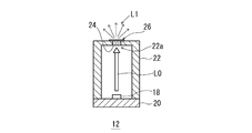
- FIG. 2 is a cross-sectional view showing a schematic configuration of a light emitting module according to the present embodiment.
- the light emitting module 12 includes a semiconductor light emitting element 18 that emits a blue laser beam, a substrate 20 on which the semiconductor light emitting element 18 is mounted, and a semiconductor light emitting element so that the laser light L0 emitted by the semiconductor light emitting element 18 does not emit in an unintended direction. It has a housing 22 for accommodating 18.
- the semiconductor light emitting device 18 preferably emits a laser beam having a peak wavelength of 380 to 480 nm, and for example, emits a blue-based (peak wavelength of about 450 nm) laser beam or a near-ultraviolet region (peak wavelength of about 405 nm). It is an element.
- the substrate 20 may also serve as a heat radiating member.
- the housing 22 is made of a material that does not transmit laser light, and an opening 22a is formed at the upper portion.
- a phosphor 24 as a wavelength conversion member that emits converted light obtained by converting the wavelength of laser light is fixed to the opening 22a.
- the phosphor 24 is, for example, a plate-shaped member made of yttrium aluminum garnet (YAG: Yttrium Aluminum Garnet) ceramics into which an activator such as cerium (Ce) has been introduced.
- the light emitting module 12 is white by mixing, for example, blue laser light emitted by the semiconductor light emitting element 18 and wavelength-converted, for example, yellow conversion light emitted by the phosphor 24 excited by the blue laser light.
- Light L1 is emitted.
- the white light L1 becomes high-intensity light having a certain degree of spread by mixing the blue laser light scattered by the phosphor 24 and the yellow wavelength-converted light having a lumbar cyan light distribution.
- the light emitting module 12 is fixed to the phosphor 24, and further includes a detection unit 26 for detecting the displacement amount of the phosphor 24.
- the detection unit 26 is configured to output an electric signal that changes according to the displacement amount of the phosphor 24.
- FIG. 3 is a cross-sectional view schematically showing the vicinity of the detection unit of the light emitting module according to the present embodiment.
- FIG. 4 is a top view schematically showing the vicinity of the detection unit of the light emitting module according to the present embodiment.
- the housing 22 has a holding portion 22b which is an insulating material surrounding the phosphor 24 fitted in the opening 22a.
- the holding portion 22b may be, for example, a ceramic material.
- the detection unit 26 is fixed to the exit surface 24a side of the phosphor 24.
- the detection unit 26 includes a wiring pattern 28 arranged on the surfaces of the holding unit 22b and the phosphor 24, an electric wire 30 connected to both ends of the wiring pattern 28, and a voltage detector 32 connected to the electric wire 30. , Have.
- the wiring pattern 28 generates a transparent conductive film 28a as an electrode formed on the emission surface 24a of the phosphor 24 and the surface 22c of the holding portion 22b, and a voltage when mechanical strain (stress) is generated.
- the piezoelectric material 28b and the piezoelectric material 28b are formed in layers.
- As the transparent conductive film 28a for example, conductive indium tin oxide (ITO: Indium Tin Oxide) is suitable. As a result, even if the wiring pattern 28 is formed on the emission surface 24a of the phosphor 24, the transmission of light is not hindered, so that the reduction in the light extraction efficiency of the light emitting module 12 as a whole is suppressed.
- ITO Indium Tin Oxide
- the piezoelectric material 28b is, for example, a thin film of zinc oxide (ZnO) having a thickness of about 3 ⁇ m.
- the piezoelectric material 28b preferably has a Curie point of 200 ° C. or higher (or 300 ° C. or higher), or a material such as ZnO that does not have a Curie point. This is because the piezoelectric material 28b may be heated by the heat generated when the phosphor 24 is excited by the laser beam L0, and if the Curie point is low, the piezoelectricity is not exhibited.
- a tensile load is applied to the YAG ceramics, it breaks at an elongation of about 4%. Therefore, in the case of the phosphor 24 of YAG ceramics having a thickness of 300 ⁇ m, it breaks when an elongation of about 12 ⁇ m occurs in the thickness direction due to a tensile load.
- the displacement amount due to thermal expansion of YAG ceramics for example, 0.36 ⁇ m
- the displacement amount caused by fracture due to the tensile load (12 ⁇ m) have a difference of 30 times or more, and the displacement amount of the phosphor is detected. Therefore, it can be estimated in advance whether or not the phosphor is likely to be destroyed.
- the piezoelectric material 28b according to the present embodiment is a ZnO thin film having a thickness of 3 ⁇ m, and has a coefficient of linear expansion of ZnO of 3.2 to 3.9 [ 10-6 / ° C.], so that the temperature change ⁇ T is 150.
- PZT lead zirconate titanate
- the coefficient of linear expansion of PZT is 2 to 4 [ 10-6 / ° C], so that the displacement when the temperature change ⁇ T is 150 ° C.
- the relationship between the displacement amount of the piezoelectric film made of PZT and the voltage is that the voltage generated by the displacement of about several ⁇ m to 10 ⁇ m is in the range of several tens V to several hundred V, and the general voltage detector 32 is used. It is sufficiently detectable. That is, when the voltage detector 32 detects a large voltage corresponding to a displacement larger than the thermal expansion of the phosphor 24 and smaller than the displacement at which breakage occurs (for example, a displacement of about 1 to 10 ⁇ m), the control unit 34 (see FIG. 3) determines that the phosphor 24 is likely to be destroyed, and stops driving the semiconductor light emitting element 18.
- the control unit 34 is, for example, an appropriate combination of an arithmetic unit, a drive circuit, and a storage circuit.
- the light emitting module 12 can estimate in advance whether or not the phosphor 24 is likely to be destroyed by detecting the displacement amount of the phosphor 24. Further, by adopting the piezoelectric material 28b as a part of the detection unit 26, the displacement amount of the phosphor 24 can be detected with a simple configuration. Further, by using a material having a Curie point of 200 ° C. or higher (or 300 ° C. or higher) or a material having no Curie point such as ZnO as the piezoelectric material 28b, even if the light emitting module 12 becomes high in temperature, the phosphor is used. It can be estimated in advance whether or not 24 is likely to be destroyed.
- the detection unit 26 can be integrally created with the phosphor 24 by laminating the transparent conductive film 28a and the piezoelectric material 28b on the phosphor 24 made of the same ceramic material.
- ZnO constituting the piezoelectric material 28b is a transparent thin film arranged so as to cover the exit surface 24a from which the light L1 converted by the phosphor 24 is emitted.
- the piezoelectric material 28b can be arranged in the region (emission surface 24a) through which the laser beam of the phosphor 24 is transmitted, and cracks and the like on the emission surface 24a of the phosphor 24 can be detected.
- the detection unit 26 similar to that of the present embodiment may be provided on the incident surface 24b side of the phosphor 24. As a result, cracks and the like on the incident surface 24b of the phosphor 24 can be detected.
- a part of the zigzag wiring pattern 28 exists on the boundary region R1 between the phosphor 24 and the holding unit 22b. Therefore, if the phosphor 24 falls off from the holding portion 22b, the displacement amount of the piezoelectric material 28b contained in a part of the wiring pattern 28 suddenly changes, and the voltage detector 32 before the wiring pattern 28 is cut. Detected as a large voltage change.
- FIG. 5 is a top view schematically showing the vicinity of the detection unit of the light emitting module according to the modified example of the present embodiment.
- the light emitting module 36 shown in FIG. 5 includes a detection unit 40 having a wiring pattern 38 formed only on the emission surface 24a of the phosphor 24.
- a detection unit 40 having a wiring pattern 38 formed only on the emission surface 24a of the phosphor 24.
- the detection unit 40 most of the wiring pattern 38 exists on the boundary region R2 between the exit surface 24a of the phosphor 24 and the holding unit 22b. Further, since the wiring pattern 38 can be shortened, the material cost for forming the detection unit can be reduced.
- FIG. 6 is a top view schematically showing the vicinity of the detection unit of the light emitting module according to another modification of the present embodiment.
- the light emitting module 42 shown in FIG. 6 does not have a wiring pattern 44 formed on the emission surface 24a of the phosphor 24. That is, most of the wiring pattern 44 is formed only on the surface 22c of the housing 22. Therefore, the light emitted from the exit surface 24a of the phosphor 24 is not obstructed.
- the holding portion 22b when the holding portion 22b is made of a ceramic material such as alumina (linear expansion coefficient 7.2 [ 10-6 / ° C]), it may be broken by thermal expansion like YAG ceramics. Even if the holding portion 22b is broken (cracked) and the phosphor 24 is dropped or broken, the voltage detector 32 detects it as a large voltage change before the wiring pattern 44 is cut. That is, by detecting the state of the holding portion 22b, it is possible to indirectly detect the falling off or breaking of the phosphor 24.
- a ceramic material such as alumina (linear expansion coefficient 7.2 [ 10-6 / ° C]
- the present invention has been described above with reference to the above-described embodiment, the present invention is not limited to the above-described embodiment, and the present invention is not limited to the above-described embodiment, and the configuration of the embodiment may be appropriately combined or replaced. It is included in the present invention. Further, it is also possible to appropriately rearrange the combination and the order of processing in the embodiment based on the knowledge of those skilled in the art, and to add modifications such as various design changes to the embodiment, and such modifications are added. Such embodiments may also be included in the scope of the present invention.
- the present invention can be used for a light emitting module using a light emitting element that emits light having a high energy density as a light source.
- Vehicle headlight unit 12 light emitting module, 18 semiconductor light emitting element, 22 housing, 22a opening, 22b holding part, 24 phosphor, 24a emitting surface, 24b incident surface, 26 detecting part, 28 wiring pattern, 28a Transparent conductive film, 28b piezoelectric material, 32 voltage detector, 34 control unit.
Landscapes
- Engineering & Computer Science (AREA)
- General Engineering & Computer Science (AREA)
- Physics & Mathematics (AREA)
- Spectroscopy & Molecular Physics (AREA)
- Optics & Photonics (AREA)
- Condensed Matter Physics & Semiconductors (AREA)
- General Physics & Mathematics (AREA)
- Electromagnetism (AREA)
- Crystallography & Structural Chemistry (AREA)
- Chemical & Material Sciences (AREA)
- Non-Portable Lighting Devices Or Systems Thereof (AREA)
- Semiconductor Lasers (AREA)
- Lighting Device Outwards From Vehicle And Optical Signal (AREA)
- Arrangement Of Elements, Cooling, Sealing, Or The Like Of Lighting Devices (AREA)
Priority Applications (1)
| Application Number | Priority Date | Filing Date | Title |
|---|---|---|---|
| JP2021526025A JPWO2020250757A1 (https=) | 2019-06-14 | 2020-06-02 |
Applications Claiming Priority (2)
| Application Number | Priority Date | Filing Date | Title |
|---|---|---|---|
| JP2019-111345 | 2019-06-14 | ||
| JP2019111345 | 2019-06-14 |
Publications (1)
| Publication Number | Publication Date |
|---|---|
| WO2020250757A1 true WO2020250757A1 (ja) | 2020-12-17 |
Family
ID=73736027
Family Applications (1)
| Application Number | Title | Priority Date | Filing Date |
|---|---|---|---|
| PCT/JP2020/021835 Ceased WO2020250757A1 (ja) | 2019-06-14 | 2020-06-02 | 発光モジュール |
Country Status (3)
| Country | Link |
|---|---|
| JP (1) | JPWO2020250757A1 (https=) |
| CN (2) | CN212481157U (https=) |
| WO (1) | WO2020250757A1 (https=) |
Cited By (1)
| Publication number | Priority date | Publication date | Assignee | Title |
|---|---|---|---|---|
| JP2020080400A (ja) * | 2018-11-13 | 2020-05-28 | 株式会社ダイセル | 光学部材、該光学部材を含むレーザーモジュール及びレーザーデバイス |
Families Citing this family (1)
| Publication number | Priority date | Publication date | Assignee | Title |
|---|---|---|---|---|
| WO2020250757A1 (ja) * | 2019-06-14 | 2020-12-17 | 株式会社小糸製作所 | 発光モジュール |
Citations (5)
| Publication number | Priority date | Publication date | Assignee | Title |
|---|---|---|---|---|
| JP2013168587A (ja) * | 2012-02-16 | 2013-08-29 | Sharp Corp | 発光装置、半導体レーザ素子、および照明装置 |
| JP2015060159A (ja) * | 2013-09-20 | 2015-03-30 | カシオ計算機株式会社 | 蛍光発光装置及びプロジェクタ |
| JP2016092288A (ja) * | 2014-11-07 | 2016-05-23 | スタンレー電気株式会社 | 光源装置及びこれを用いた照明装置 |
| US20160290856A1 (en) * | 2015-04-01 | 2016-10-06 | Osram Gmbh | Device and method for light conversion device monitoring |
| JP2018002912A (ja) * | 2016-07-04 | 2018-01-11 | 株式会社小糸製作所 | 焼結体および発光装置 |
Family Cites Families (6)
| Publication number | Priority date | Publication date | Assignee | Title |
|---|---|---|---|---|
| JP4975797B2 (ja) * | 2009-10-14 | 2012-07-11 | シャープ株式会社 | 照明装置、車両用灯具および車両 |
| GB2493135A (en) * | 2011-07-14 | 2013-01-30 | Barco Nv | Orbiting wavelength conversion element |
| JP6504886B2 (ja) * | 2015-04-03 | 2019-04-24 | 株式会社小糸製作所 | 車両用灯具 |
| KR20170018493A (ko) * | 2015-07-28 | 2017-02-20 | 에스엘 주식회사 | 차량용 램프 |
| CN107062128A (zh) * | 2017-06-09 | 2017-08-18 | 超视界激光科技(苏州)有限公司 | 一种自适应照明灯 |
| WO2020250757A1 (ja) * | 2019-06-14 | 2020-12-17 | 株式会社小糸製作所 | 発光モジュール |
-
2020
- 2020-06-02 WO PCT/JP2020/021835 patent/WO2020250757A1/ja not_active Ceased
- 2020-06-02 JP JP2021526025A patent/JPWO2020250757A1/ja active Pending
- 2020-06-04 CN CN202021004687.3U patent/CN212481157U/zh active Active
- 2020-06-04 CN CN202010500192.8A patent/CN112082132B/zh active Active
Patent Citations (5)
| Publication number | Priority date | Publication date | Assignee | Title |
|---|---|---|---|---|
| JP2013168587A (ja) * | 2012-02-16 | 2013-08-29 | Sharp Corp | 発光装置、半導体レーザ素子、および照明装置 |
| JP2015060159A (ja) * | 2013-09-20 | 2015-03-30 | カシオ計算機株式会社 | 蛍光発光装置及びプロジェクタ |
| JP2016092288A (ja) * | 2014-11-07 | 2016-05-23 | スタンレー電気株式会社 | 光源装置及びこれを用いた照明装置 |
| US20160290856A1 (en) * | 2015-04-01 | 2016-10-06 | Osram Gmbh | Device and method for light conversion device monitoring |
| JP2018002912A (ja) * | 2016-07-04 | 2018-01-11 | 株式会社小糸製作所 | 焼結体および発光装置 |
Cited By (1)
| Publication number | Priority date | Publication date | Assignee | Title |
|---|---|---|---|---|
| JP2020080400A (ja) * | 2018-11-13 | 2020-05-28 | 株式会社ダイセル | 光学部材、該光学部材を含むレーザーモジュール及びレーザーデバイス |
Also Published As
| Publication number | Publication date |
|---|---|
| JPWO2020250757A1 (https=) | 2020-12-17 |
| CN112082132B (zh) | 2023-05-16 |
| CN212481157U (zh) | 2021-02-05 |
| CN112082132A (zh) | 2020-12-15 |
Similar Documents
| Publication | Publication Date | Title |
|---|---|---|
| JP5841126B2 (ja) | 発光装置、照明装置、前照灯および車両 | |
| TW578315B (en) | Luminescence-diode | |
| CN101627326B (zh) | 带有半导体芯片和导光层的装置 | |
| JP6702349B2 (ja) | 発光装置 | |
| EP2458266B1 (en) | Light emitting diode (LED) lamp | |
| JP5220753B2 (ja) | 発光ダイオード照明装置 | |
| CN103486542A (zh) | 光源装置及照明装置 | |
| CN102714204B (zh) | 照明装置 | |
| TWI603033B (zh) | 包含熱導體之發光模組、燈及燈具 | |
| JP2011014535A (ja) | 照明装置 | |
| JP2016122715A (ja) | 半導体発光装置及びその駆動方法 | |
| JP5285688B2 (ja) | 発光装置、照明装置および車両用前照灯 | |
| JP6112782B2 (ja) | 照明装置 | |
| CN101128942B (zh) | Led阵列 | |
| WO2020250757A1 (ja) | 発光モジュール | |
| JP5491691B2 (ja) | 発光装置および照明器具 | |
| JP2010267851A (ja) | 発光モジュール、発光モジュールの製造方法、および灯具ユニット | |
| WO2010103840A1 (ja) | 発光モジュール、および灯具ユニット | |
| US10508791B2 (en) | Conversion of primary light into secondary light by means of a wavelength converter | |
| JP2016072263A (ja) | 発光モジュールおよび照明装置 | |
| JP4600668B2 (ja) | 面状照明装置 | |
| JP2024150736A (ja) | 発光装置、又は、光学部材 | |
| JP2014011461A (ja) | 発光ダイオードライトバー | |
| JP2017017176A (ja) | Ledモジュールおよび照明装置 | |
| JP2010504638A (ja) | 張力緩和を備える発光装置 |
Legal Events
| Date | Code | Title | Description |
|---|---|---|---|
| 121 | Ep: the epo has been informed by wipo that ep was designated in this application |
Ref document number: 20822669 Country of ref document: EP Kind code of ref document: A1 |
|
| ENP | Entry into the national phase |
Ref document number: 2021526025 Country of ref document: JP Kind code of ref document: A |
|
| NENP | Non-entry into the national phase |
Ref country code: DE |
|
| 122 | Ep: pct application non-entry in european phase |
Ref document number: 20822669 Country of ref document: EP Kind code of ref document: A1 |