WO2020246015A1 - 光検査装置 - Google Patents
光検査装置 Download PDFInfo
- Publication number
- WO2020246015A1 WO2020246015A1 PCT/JP2019/022656 JP2019022656W WO2020246015A1 WO 2020246015 A1 WO2020246015 A1 WO 2020246015A1 JP 2019022656 W JP2019022656 W JP 2019022656W WO 2020246015 A1 WO2020246015 A1 WO 2020246015A1
- Authority
- WO
- WIPO (PCT)
- Prior art keywords
- component
- optical inspection
- birefringent element
- sample
- inspection device
- Prior art date
- Legal status (The legal status is an assumption and is not a legal conclusion. Google has not performed a legal analysis and makes no representation as to the accuracy of the status listed.)
- Ceased
Links
Images


Classifications
-
- G—PHYSICS
- G01—MEASURING; TESTING
- G01B—MEASURING LENGTH, THICKNESS OR SIMILAR LINEAR DIMENSIONS; MEASURING ANGLES; MEASURING AREAS; MEASURING IRREGULARITIES OF SURFACES OR CONTOURS
- G01B11/00—Measuring arrangements characterised by the use of optical techniques
- G01B11/30—Measuring arrangements characterised by the use of optical techniques for measuring roughness or irregularity of surfaces
-
- G—PHYSICS
- G01—MEASURING; TESTING
- G01B—MEASURING LENGTH, THICKNESS OR SIMILAR LINEAR DIMENSIONS; MEASURING ANGLES; MEASURING AREAS; MEASURING IRREGULARITIES OF SURFACES OR CONTOURS
- G01B9/00—Measuring instruments characterised by the use of optical techniques
- G01B9/02—Interferometers
Definitions
- the present invention relates to an optical inspection device that inspects a sample using light.
- optical interference technology This is a technique using differential interference contrast, in which two coherent beams generated by a birefringent element scan the surface of a semiconductor sample. Defects on the sample surface are inferred from the phase shift that occurs when the two beams hit the non-flat region.
- a calibration procedure of an optical microscope This is because the average height of the wafer is determined by the calibration procedure, and this average height is compared with the surface unevenness to identify defects. Since the flatness evaluation of the sample relies on the phase difference between the two probe beams, it is important to prevent as much as possible the phase distortion effect that can cause errors during detection. Therefore, in order to operate under favorable conditions, it is necessary to control the phase shift between the two probe beams and correct the phase shift that may occur during wafer inspection. This phase shift is caused by, for example, vibration, mechanical drift, temperature drift, and the like.
- Patent Document 1 describes a mechanism for adjusting the phase of an optical beam separated into two optical paths.
- the phase difference adjusting mechanism sets the phase difference between the light of the first polarized light and the light of the second polarized light.
- the phase difference between the two beams is changed by the rotating polarizing plate unit.
- Patent Document 2 describes an interference observation device.
- the device includes a beam splitter that splits the initial beam into P and S polarization components.
- the first separation beam passes through the sample to be analyzed and recombines with the second separation beam to cause interference.
- the intensity of the recombination signal is adjusted by rotating the plane of polarization of the first separation beam.
- the document does not describe adjusting the phase difference.
- the parameters to be measured are estimated from the phase characteristics of the interference beam. Analyze the phase information and convert it into physical parameters. Therefore, if the phase shift between the interference beams has a component not caused by the parameter to be measured (for example, a component caused by noise or vibration), an extra phase shift occurs in the detection signal. This is a factor that impairs the robustness of the measuring device. Therefore, it is necessary to control the phase shift so that the extra phase shift does not cause a detection error.
- the initial beam is separated into, for example, a P-polarized light component and an S-polarized light component.
- the P-polarized beam and the S-polarized beam are used to scan the material to be inspected and finally recombine the beams to generate an interference pattern.
- the birefringent element has different propagation characteristics depending on the polarization characteristics of light, the two beams pass through different optical paths, and the initial phase difference between the two beams even before the material to be inspected is irradiated. Exists.
- the two beams are physically separated and propagate parallel to each other. At this time, both beams are separated from each other by the shear amount ⁇ . This shear amount is determined according to the characteristics of the system including the birefringence element and the collimating lens.
- phase shift between the separated beams carries only information about surface flatness.
- the inclusion of another phase shift causes errors in the reconstruction process by distorting the original signal or causing saturation.
- Factors such as vibration and noise are variable and cannot be completely zeroed, so extra phase shifts can be applied to the signal, which causes some drift in the reconstruction process.
- phase shift factors are compensated for by performing an initial calibration of the system. However, these factors change over time, resulting in a phase shift that did not exist in the initial state. In addition to this, another source of noise may occur during the sample surface scan.
- phase shift that causes signal distortion in the wafer surface flatness reconstruction process may appear. Therefore, it is conceivable to compensate for the influence of all these factors on the phase of the signal by causing a phase shift in the opposite direction and returning the phase level to the calibration value without interrupting the scanning operation.
- the present invention has been made in view of the above problems, and provides a technique for automatically correcting this phase difference at the time of inspection by analyzing the influence of the phase difference while shifting the position of the birefringent element.
- the purpose is.
- the optical measuring device adjusts the optical path of each beam by moving a birefringent element that separates the laser beam emitted by the laser source into two beams, thereby adjusting the phase difference between the beams. ..
- the detection accuracy can be significantly improved, and the robustness against noise such as thermal effect and vibration generated with the passage of time can be enhanced. Issues, configurations, and effects other than those described above will be clarified by the description of the following embodiments.
- the present invention proposes a method for correcting the influence of external noise on a detection signal in an optical interference system.
- the basic idea of the present invention is to compensate for the phase shift caused by noise such as thermal effect or vibration by additionally giving a phase shift to the signal. In other words, the present invention cancels an unnecessary phase shift by giving a phase shift in the opposite direction.
- the birefringent element is placed on the moving stage in order to scan the position of the birefringent element.
- the computer remotely controls the position of the moving stage by monitoring the position of the birefringent element by the DC level of the detection signal. If this signal level is sufficiently close to the initial calibration level, the birefringence element is not moved.
- the software automatically starts scanning the position of the birefringence element. Then, the DC level of the detection signal is returned to the vicinity of the calibration state. This position scan is performed within the range of 10 to 100 micrometers and can be performed without interrupting the sample scanning process.
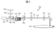
- FIG. 1 is a configuration diagram of an optical inspection device 100 according to an embodiment of the present invention.
- the optical inspection device 100 is a device that optically inspects defects on the surface of the sample 115.
- the optical inspection device 100 includes a laser source 101, a polarizing beam splitter 103, a quarter wave plate 106, a lens group (objective lens 109, an imaging lens 105, relay lenses 110 and 113), a mirror 114, a detector 104, and birefringence. It includes an element 107 and a moving stage 108.
- the birefringence element 107 is connected to the moving stage 108 (for example, placed and fixed on the moving stage 108), and the moving stage 108 can adjust the position of the birefringence element 107 on the order of micrometers.
- the laser source 101 emits the laser beam 102.
- the laser beam 102 passes through a polarizing beam splitter 103, passes through a quarter wave plate 106, becomes an elliptically polarized state, and is separated into a P-polarized beam 111 and an S-polarized beam 112 by passing through a birefringent element 107. ..
- These two beams are separated from each other over a distance of shear amount ⁇ and are used to scan the surface of sample 115.
- the detector 104 detects the interference pattern via the image pickup lens 105.
- the detector 104 outputs a detection signal I representing the result of detecting the interference signal.
- the detection signal I contains information represented by the phase difference between the P-polarized beam 111 and the S-polarized beam 112. With this configuration, the phase difference between the two beams reflected from the surface of the sample 115 can be converted into a current signal. This current signal can be used to reconstruct the flatness of the sample 115 surface.
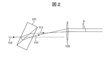
- FIG. 2 is a diagram showing a beam separation process by the birefringent element 107.
- the elliptically polarized laser beam 102 is separated into a P-polarized beam 111 and an S-polarized beam 112 when passing through the birefringent element 107.
- These two beams are collimated by the objective lens 109 and propagate in parallel optical paths separated from each other by the shear amount ⁇ . Since the propagation conditions differ depending on the polarization state, the phase shift between the separated beams depends on the optical path difference.
- the shear amount ⁇ is determined by the intrinsic characteristics of the birefringent element 107, and this is fixed for each birefringent element 107.
- These separated beams are applied to the sample 115, and the sample surface is scanned as a probe beam.
- the beam scans the sample surface if the irradiation position is in a flat region, the two beams are reflected with a constant phase difference, and no phase shift or signal intensity fluctuation is observed. If there is any defect on the surface of the sample, the optical path length of one beam will be different from the optical path length of the other, and the phase difference caused by this will change the signal intensity of the detection signal I from the initial value. This indicates that there are defects on the sample surface.
- I off is a signal intensity representing the average height of the sample surface. That is, it is the surface height at the place where there is no defect. In other words, this represents the flatness level of the sample.
- ⁇ is the laser wavelength.
- I 0 is the signal amplitude.
- ⁇ is a phase shift obtained when two beams hit a region where the uneven height of the sample surface is ⁇ h.
- FIG. 3 is a schematic view showing how a beam is irradiated to a defect on the sample surface. Cases 1 to 5 described below may occur in the process of the beam scanning the sample surface.
- FIG. 4 is a schematic view showing how the detection signal I changes as the probe beam scans the sample surface.
- the beam passes through the flat region 403, the bump 404, and the hole 405, respectively.
- the detection signal I fluctuates to a value higher or lower than I off with the unevenness of the surface height.
- the signal output by the detector shall represent the surface condition of the sample by changing the signal intensity when the beam hits a defect.
- the operation of extracting the surface height is represented by the following equation 2. This equation expresses the wafer surface level ⁇ h by the inverse sine function by the function of the phase shift ⁇ between the probe beams.
- Equation 3 is an equation representing the detection signal in consideration of the unnecessary phase component ⁇ corresponding to all noise sources that cause a phase shift of the detection signal.
- the influence of ⁇ can be compensated according to the initial phase shift between the separated beams.
- the phase shift ⁇ between the probe beams becomes zero, which is called the optimum position.
- the detection signal becomes a constant value during sample scanning, and the detection signal fluctuates only when there is a height change on the sample surface.
- the present invention compensates for the drift of ⁇ by adding a compensating phase shift ⁇ so that the phase shift relies solely on ⁇ h.
- Equation 4 As shown in Equation 4 below, ⁇ is added to the equation of the detection signal I. Therefore, there are three factors that affect the phase of the signal: the component ⁇ h due to defects existing on the wafer surface; the component ⁇ due to noise; the shift added by moving the birefringence element 107. ⁇ .
- the state at this time is shown in Equation 5 below.
- the phase of the detection signal I is ⁇ + ⁇ .
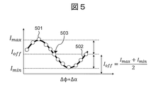
- FIG. 5 is a diagram schematically showing the influence of the position of the birefringent element 107 on the phase shift between the separated beams.
- the intensity of the detection signal I at each position of the birefringence element 107 is, for example, dot 501, forming a sinusoidal curve 502.
- the additional phase shift ⁇ generated by scanning the birefringent element 107 accurately compensates for the phase shift ⁇ caused by noise or vibration.
- the only phase component remaining in the sinusoidal function is ⁇ h with respect to the wafer surface level.
- ⁇ h is 0 in the flat region and is a value other than 0 in other positions.
- the birefringence element 107 is mounted on a moving stage 108 that is software controlled.
- the position where the laser beam is incident on the birefringent element 107 shifts according to the position of the birefringent element 107.
- the moving stage 108 allows the position of the birefringent element 107 to be moved within a range of several micrometers.
- the moving direction of the birefringent element 107 is a direction parallel to the direction in which the P-polarized beam 111 and the S-polarized beam 112 are separated from each other. By scanning the position of the birefringent element 107, the phase shift between the P-polarized beam 111 and the S-polarized beam 112 can be changed.
- the optical inspection device 100 searches for the position of the birefringent element 107 so that the detection signal I is equal to I off at the position without defects.
- phase shift correction operation is performed by a mechanism that moves the birefringent element 107 at a low speed or in a step operation until the DC level reaches I off .
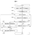
- FIG. 6 is a flowchart illustrating a procedure in which the optical inspection device 100 corrects the phase shift. Each step of FIG. 6 will be described below.
- Steps S601 to S602 The user measures the average surface height of the sample 115 by performing an initial calibration procedure on the optical test apparatus 100 (S601). This will define I off .
- the user further sets the tolerance threshold of I off (S602).
- the permissible threshold represents the range in which the DC level of the detection signal should be maintained. For example, 5%, 10%, etc. can be set as an allowable threshold value with respect to the initial value of I off .
- Steps S603 to S604 The optical inspection apparatus 100 scans the surface of the sample 115 once (S603).
- the scanning range at this time is, for example, a counter-reciprocation from one end of the sample surface to the other end.
- the detector 104 extracts the DC component of the detection signal I (S604).
- Step S605 The detector 104 determines whether or not the DC component extracted in S604 is within the allowable threshold range. That is, it is determined whether or not the DC component of the detection signal I deviates from I off . If it is within the allowable threshold range, the process proceeds to step S606, and if it is outside the range, the process proceeds to step S607.
- Step S606 The optical inspection apparatus 100 repeats S603 to S605 until the entire surface of the sample 115 is scanned. When the entire surface has been scanned, this flowchart ends.
- Steps S607 to S609 The moving stage 108 starts scanning the position of the birefringent element 107 (S607). The moving stage 108 continues the operation until the optimum position 503 described with reference to FIG. 5 is obtained (S608). If the optimum position 503 is obtained, the moving stage 108 maintains that position and returns to step S603.
- Step S608 Method 1 for determining the optimum position 503
- the detector 104 determines the position of the birefringence element 107 (first position) when the detection signal I takes the maximum value and the position of the birefringence element 107 when the detection signal I takes the minimum value (second position). Position) and are specified respectively.
- the detector 104 can identify the optimum position 503 according to these positions. For example, the centers of both positions can be regarded as the optimum position 503.
- the maximum value and the minimum value can be specified, for example, by the position where the differential value of the detection signal I becomes 0.
- Step S608 Method 2 for determining the optimum position 503
- the detector 104 can consider the position where the differential value of the detection signal I is the maximum or the minimum (the steepest position) as the optimum position.
- the maximum differential value is when the detection signal I increases from the minimum value to the maximum value
- the minimum differential value is when the detection signal I decreases from the maximum value to the minimum value. It is when you are.
- the phase shift correction process is started immediately when the DC level drift in the detection signal is detected to correct the phase shift, and the surface height is the allowable threshold value. It should be within range and not interfere with the sample scanning process.
- the optical inspection apparatus 100 In order to maintain the DC level of the detection signal I at I off , the optical inspection apparatus 100 continuously performs a minute phase shift correction by a minute position scan of the birefringence element 107. This makes it possible to correct the phase shift due to noise without interrupting the sample inspection process.
- the present invention is not limited to the above-described examples, and includes various modifications.
- the above-described examples have been described in detail in order to explain the present invention in an easy-to-understand manner, and are not necessarily limited to those having all the described configurations. Further, it is possible to replace a part of the configuration of one embodiment with the configuration of another embodiment, and it is also possible to add the configuration of another embodiment to the configuration of one embodiment. Further, it is possible to add / delete / replace a part of the configuration of each embodiment with another configuration.
- the moving stage 108 moves the birefringence element 107 to the optimum position 503 to eliminate the phase shift caused by noise.
- the phase shift can be suppressed to a certain level or less, it can be said that there is no problem in practical use.
- the optical inspection device 100 can suppress the phase shift to a range corresponding to the detection resolution or less at which the surface height of the sample 115 can be detected, the object of the present invention can be sufficiently achieved.
- the detector 104 specifies the optimum position 503. This can be realized, for example, by integrally configuring an arithmetic unit that analyzes the detection signal output by the detector 104 with the detector 104.
- the present invention is not limited to this, and the detector 104 and the arithmetic unit may be configured separately. Further, the arithmetic unit may be used as a control device for controlling each part of the optical inspection device 100.
- a Nomalski prism or a Wollaston prism can be used as the birefringent element 107.
- Other optical elements may be used. That is, any other element can be used as long as it is a birefringent element that separates the laser beam 102 by a shear amount ⁇ .
- the moving stage 108 can move the position of the birefringent element 107 by, for example, a stepping motor. Since the stepping motor can move the position step by step, there is an advantage that it is convenient to acquire the plot points described with reference to FIG. 5 for each position of the birefringence element 107.
- the optical inspection device 100 is configured as a differential interference optical system, but the present invention can also be used in other optical systems. That is, the advantages of the present invention can be obtained if the optical system separates the laser beam 102 into two beams by the birefringence element 107 and irradiates the sample 115.
- Optical inspection device 101 Laser source 103: Polarized beam splitter 104: Detector 105: Imaging lens 106: 1/4 wave plate 107: Birefringence element 108: Moving stage 109: Objective lens 111: P polarized beam 112: S-polarized beam 114: Mirror 115: Sample
Landscapes
- Physics & Mathematics (AREA)
- General Physics & Mathematics (AREA)
- Investigating Materials By The Use Of Optical Means Adapted For Particular Applications (AREA)
- Length Measuring Devices By Optical Means (AREA)
Abstract
本発明は、複屈折素子の位置をシフトさせながら位相差の影響を分析することにより、検査時においてこの位相差を自動的に補正する技術を提供することを目的とする。本発明に係る光計測装置は、レーザ源が出射したレーザビームを2つのビームに分離する複屈折素子を移動させることにより、各ビームの光路を調整し、これによりビーム間の位相差を調整する(図1参照)。
Description
本発明は、光を用いて試料を検査する光検査装置に関する。
半導体デバイスの微細化が社会における重要な役割を果たすようになるのにともない、半導体の表面を検査および評価することが必要になっている。具体的には、半導体表面の平坦特性をサブマイクロメートルオーダで検査することが必要である。欠陥を正確に検出し表面欠陥を正確に識別することは、半導体デバイスの良好な品質と、安全かつ高信頼な利用を確保するための、基本的な処理である。
従来の半導体ウエハを検査するための光システムは通常、光干渉技術を用いる。これは差分干渉コントラストを用いる技術であり、複屈折素子が生成した2つのコヒーレントビームが半導体サンプルの表面を走査する。サンプル表面上の欠陥は、2つのビームが非平坦領域に当たったとき生じる位相シフトから推測される。ウエハ表面検査を効率的に実施するとともに欠陥を正確に検出するためには、光学顕微鏡の較正手順を実施する必要がある。較正手順により、ウエハの平均高さを判定し、この平均高さを表面凹凸と比較して欠陥を識別するからである。サンプルの平坦性評価は2つのプローブビーム間の位相差に依拠しているので、検出時におけるエラーを生じさせる可能性がある位相歪み効果をできる限り防ぐことが重要である。したがって良好な状況下で動作するためには、2つのプローブビーム間の位相シフトを制御するとともに、ウエハ検査中に生じる可能性がある位相シフトを補正する必要がある。この位相シフトは例えば、振動、機械的ドリフト、温度ドリフトなどに起因するものである。
下記特許文献1は、2つの光路に分離された光ビームの位相を調整する機構について記載している。位相差調整機構は、第1偏光の光と第2偏光の光との間の位相差をセットする。2つのビーム間の位相差は、回転偏光板ユニットによって変更される。
下記特許文献2は、干渉観察装置について記載している。同装置は、初期ビームをP偏光成分とS偏光成分へ分離するビームスプリッタを備えている。第1分離ビームは、分析する試料を通過し、第2分離ビームと再結合して干渉を生じさせる。第1分離ビームの偏光面を回転させることにより、再結合信号の強度を調整する。同文献は、位相差を調整することについては記載していない。
光干渉計測システムにおいて、計測するパラメータは、干渉ビームの位相特性から推定される。位相情報を分析して、物理パラメータに変換する。したがって、干渉ビーム間の位相シフトが、計測しようとしているパラメータに起因しない成分(例えばノイズや振動に起因する成分)を有している場合、検出信号において余分な位相シフトが生じる。これは計測デバイスのロバスト性を損ねる要因となる。したがって、位相シフトを制御することにより、余分な位相シフトが検出エラーを生じさせないようにすることが必要である。
光が通過するときビームを分離する複屈折素子によって干渉ビームを生成するシステムにおいて、初期ビームは例えばP偏光成分とS偏光成分に分離される。このP偏光ビームとS偏光ビームを用いて、検査する材料を走査し、最終的にビームを再結合して干渉パターンを生成する。複屈折素子は、光の偏光特性によって異なる伝搬特性を有するので、2つのビームは異なる光路を通過し、検査する材料に対して照射される前の時点においても2つのビーム間には初期位相差が存在する。さらに、2つのビームは物理的に分離され、互いに平行に伝搬する。このとき両ビームは、シャー量δだけ互いに離れている。このシャー量は、複屈折素子とコリメートレンズを備えるシステムの特性に応じて定まる。
2つのビームを用いてサンプルの平坦性を検査する場合、サンプル表面高さの変動によって生じる位相シフトが見られ、材料の特性は干渉信号を検出することにより再構築することができる。信号強度の変化をその初期値と比較することにより、スキャン領域表面を再構築することができる:信号強度の強弱は、ビームが高低領域に当たるのにともなって生じる。
検出プロセスは、干渉信号から抽出した位相情報に依拠しているので、分離ビーム間の位相シフトが表面平坦性についての情報のみを確実に搬送するようにすることが、重要である。別の位相シフトが含まれていると、元の信号を歪ませたりあるいは飽和現象を生じさせたりすることにより、再構築プロセスにおいてエラーが生じる。振動やノイズなどの要因は様々であり完全にゼロにはできないので、余分な位相シフトが信号に対して付与される可能性があり、これにより再構築プロセスにおいて何らかのドリフトが生じる。
干渉ベース検出器などの光学システムにおいては、様々なノイズ要因があり、これらは全て固有の影響を検出信号の位相に対して与える。例えば物理的振動、レーザパワー不安定、レンズ/複屈折素子/ミラーなどに対する熱効果、などである。これらはそれぞれ独立して信号位相に対して影響を与え、それぞれの影響を推測するのは現実的に不可能である。これらの不要な位相シフトの要因は、システムの初期較正を実施することによって補償される。しかしこれら要因は時間経過にともなって変化し、初期状態においては存在していなかった位相シフトが生じる。これに加えて、サンプル表面スキャンを実施している間において、別のノイズ源が生じる可能性がある。
例えば、微小な位置ずれやドリフト、光学部品を膨張させる熱効果、あるいはレーザパワー不安定は、時間経過にともなってそれぞれ独立して徐々に生じる場合がある。その結果、ウエハ表面平坦性の再構築プロセスにおける信号歪みを生じさせるだけの位相シフトが現れる可能性がある。そこで、スキャン動作を中断させることなく、反対向きの位相シフトを生じさせて位相レベルを較正値まで戻すことにより、信号の位相に対するこれら全ての要因の影響を補償することが考えられる。
複屈折素子を通過する光は、偏光状態に応じて異なる光路を伝搬する。そこで、複屈折素子の位置を微小移動させることにより位相シフトを追加で生じさせることにより、上記様々なノイズ要因によって生じた位相シフトを全て補償することが考えられる。
上記各特許文献記載のような従来技術は、光干渉デバイスにおける位相差を測定し補正することについて言及している。しかし、光源から出射されたビームを2つのビームに分離する複屈折素子の位置を微調整することにより、ビーム間の位相差を補正する構成については、考慮されていない。
本発明は、上記課題に鑑みてなされたものであり、複屈折素子の位置をシフトさせながら位相差の影響を分析することにより、検査時においてこの位相差を自動的に補正する技術を提供することを目的とする。
本発明に係る光計測装置は、レーザ源が出射したレーザビームを2つのビームに分離する複屈折素子を移動させることにより、各ビームの光路を調整し、これによりビーム間の位相差を調整する。
本発明に係る光計測装置によれば、検出精度を大幅に向上させることができるとともに、時間経過にともなって生じる熱効果や振動などのノイズに対するロバスト性を高めることができる。上記した以外の課題、構成、および効果は、以下の実施形態の説明により明らかにされる。
<本発明の基本原理について>
本発明は、光干渉システムにおける検出信号に対する外部ノイズの影響を補正する方法を提案する。本発明の基本的思想は、信号に対して位相シフトを追加で与えることにより、熱効果や振動などのノイズによって生じた位相シフトを補償することである。換言すると本発明は、反対向きの位相シフトを与えることにより、不要な位相シフトをキャンセルするものである。
本発明は、光干渉システムにおける検出信号に対する外部ノイズの影響を補正する方法を提案する。本発明の基本的思想は、信号に対して位相シフトを追加で与えることにより、熱効果や振動などのノイズによって生じた位相シフトを補償することである。換言すると本発明は、反対向きの位相シフトを与えることにより、不要な位相シフトをキャンセルするものである。
複屈折素子によってビームが分離される方向に対して平行な方向(コリメートされた分離ビームが試料に対して出射される方向に対して垂直な方向)に、複屈折素子の位置を走査することにより、分離ビーム間において位相シフトが追加付与される。その結果、P偏光ビームの光路とS偏光ビームの光路はそれぞれ異なることとなり、検出信号に対して所望の位相シフトが与えられる。ノイズによって位相シフトが生じると、検出信号のDCレベルに対してドリフトが生じる。したがってこの位相シフトを推定する手段としては、検出信号のDCレベルを、最初の較正手順において定義した初期値と比較することが挙げられる。検出信号のDCレベルによって複屈折素子の位置をモニタリングし、サンプル検査プロセス全体を通じて、検出信号を安定かつ初期較正値と一致するように維持する。
複屈折素子の位置を走査するために、複屈折素子を移動ステージ上に載置する。コンピュータは、検出信号のDCレベルによって複屈折素子の位置をモニタリングすることにより、移動ステージの位置を遠隔制御する。この信号レベルが初期較正レベルに対して十分近ければ、複屈折素子を移動させない。サンプル平坦性検査プロセスが進むのにともなって、ノイズや振動によりDCレベルが初期値から大きく逸脱すると(ユーザが定めた許容公差を超えると)、ソフトウェアは複屈折素子の位置走査を自動的に開始して、検出信号のDCレベルを較正状態近傍まで戻す。この位置走査は10~100マイクロメートルの範囲内で実施され、サンプル走査プロセスを中断させることなく実行することができる。
試料表面上の欠陥が比較的少なければ、検出信号の平均DCレベルは大きく変動しない。したがってこの位相シフト補償動作を実行したとしても、通常の飼料検査動作に対する影響は生じない。
<実施形態:システム構成>
図1は、本発明の実施形態に係る光検査装置100の構成図である。光検査装置100は、試料115の表面上の欠陥を光学的に検査する装置である。光検査装置100は、レーザ源101、偏光ビームスプリッタ103、4分の1波長板106、レンズ群(対物レンズ109、撮像レンズ105、リレーレンズ110と113)、ミラー114、検出器104、複屈折素子107、移動ステージ108を備える。複屈折素子107は移動ステージ108と接続され(例えば移動ステージ108上に載置して固定されている)、移動ステージ108は複屈折素子107の位置をマイクロメートルオーダで調整することができる。
図1は、本発明の実施形態に係る光検査装置100の構成図である。光検査装置100は、試料115の表面上の欠陥を光学的に検査する装置である。光検査装置100は、レーザ源101、偏光ビームスプリッタ103、4分の1波長板106、レンズ群(対物レンズ109、撮像レンズ105、リレーレンズ110と113)、ミラー114、検出器104、複屈折素子107、移動ステージ108を備える。複屈折素子107は移動ステージ108と接続され(例えば移動ステージ108上に載置して固定されている)、移動ステージ108は複屈折素子107の位置をマイクロメートルオーダで調整することができる。
レーザ源101は、レーザビーム102を出射する。レーザビーム102は偏光ビームスプリッタ103を通過し、4分の1波長板106を通過して楕円偏光状態となり、複屈折素子107を通過することによりP偏光ビーム111とS偏光ビーム112へ分離される。これら2つのビームは、シャー量δの距離を介して互いに分離されており、試料115の表面を走査するために用いられる。2つのビームが試料115表面から反射すると、これらビームは干渉し、検出器104は撮像レンズ105を介してその干渉パターンを検出する。検出器104は、干渉信号を検出した結果を表す検出信号Iを出力する。検出信号Iは、P偏光ビーム111とS偏光ビーム112との間の位相差によって表される情報を含んでいる。この構成により、試料115表面から反射した2つのビーム間の位相差を電流信号に変換することができる。この電流信号を用いて、試料115表面の平坦特性を再構築することができる。
図2は、複屈折素子107によるビーム分離過程を示す図である。楕円偏光のレーザビーム102は、複屈折素子107を通過するとき、P偏光ビーム111とS偏光ビーム112へ分離される。これら2つのビームは対物レンズ109によってコリメートされ、シャー量δだけ互いに離れた平行光路を伝搬する。伝搬条件は偏光状態によって異なるので、分離ビーム間の位相シフトは光路差に依拠する。シャー量δは複屈折素子107の内在的特性によって定まり、これは複屈折素子107ごとに固定されている。
これら分離ビームは試料115に対して照射され、試料表面をプローブビームとして走査する。ビームが試料表面を走査すると、その照射位置が平坦領域であれば、2つのビームは一定の位相差をともなって反射され、位相シフトや信号強度変動は見られない。試料表面上に何らかの欠陥がある場合、一方のビームの光路長は他方の光路長とは異なることとなり、これによって生じる位相差が検出信号Iの信号強度を初期値から変動させる。これは試料表面上に欠陥が存在することを表している。
<実施形態:ノイズをキャンセルする手順>
2つのプローブビーム間の干渉信号に基づく欠陥の理論的予測は、式1の検出信号Iによって与えられる。Ioffは、試料表面の平均高さを表す信号強度である。すなわち欠陥が存在しない箇所における表面高さである。換言すると、これは試料の平坦レベルを表している。λはレーザ波長である。I0は信号振幅である。Δθは、試料表面の凹凸高さがΔhである領域に対して2つのビームが当たったとき得られる位相シフトである。
2つのプローブビーム間の干渉信号に基づく欠陥の理論的予測は、式1の検出信号Iによって与えられる。Ioffは、試料表面の平均高さを表す信号強度である。すなわち欠陥が存在しない箇所における表面高さである。換言すると、これは試料の平坦レベルを表している。λはレーザ波長である。I0は信号振幅である。Δθは、試料表面の凹凸高さがΔhである領域に対して2つのビームが当たったとき得られる位相シフトである。

図3は、試料表面上の欠陥に対してビームを照射する様子を示す模式図である。ビームが試料表面をスキャンする過程において、以下に説明するケース1~ケース5が生じる可能性がある。
(ケース1)表面が平坦である場合:この場合、ビーム間の位相差は生じず、信号強度レベルは変化しない。この場合はΔh=0、I=Ioffである。これは、P偏光ビーム111とS偏光ビーム112との間の位相差Δθが0である場合に相当する。この状態を初期状態とし、不要な位相シフトを補償する際における基準レベルとして用いる。
(ケース2)試料の平坦面305から突出したバンプ303が存在する場合:2つのビームが試料表面に当たると、正方向の位相シフトが生じ、これらが加算的干渉して検出信号Iの信号強度が上昇する。検出器はこの信号変化を検出し、その出力信号は平坦箇所における一定値I=Ioffと比較して大きい。検出信号の正方向シフトによって、ウエハ表面の高さ304が記録される。
(ケース3)表面が平坦レベルに戻る場合(Δh<0):この場合におけるΔhの変化により、検出信号は、平坦部分の値I=Ioffへ戻る前に、負方向のドリフトを示す。このプロセスは上記ケース2の反対である。2つのビーム間で負方向の位相シフトが生じ、相殺的干渉する。これにより検出信号強度が減少し、平均値Ioffへ戻る。
(ケース4)表面に穴がある場合:この場合はケース3と同様である。検出信号の負方向ドリフトが記録される。検出信号は通常、Ioffよりも小さくなる。
(ケース5)表面が穴から平均レベルに戻る場合:この場合はケース2と同様であり、検出信号は平均レベルIoffへ戻る。
図4は、プローブビームが試料表面を走査するのにともなって検出信号Iが変化する様子を示す概略図である。ビームは、平坦領域403、バンプ404、穴405をそれぞれ通過する。検出信号Iは、表面高さの凹凸にともなって、Ioffよりも高い値や低い値へ変動する。
説明を簡略化するため、検出器が出力する信号は、ビームが欠陥に当たったとき信号強度が変化することにより、試料の表面状態を表しているものとする。表面高さを抽出する動作は、下記式2で表される。この式は逆正弦関数により、ウエハ表面レベルΔhを、プローブビーム間の位相シフトΔθの関数によって表す。

しかしこの理論的状況は、ノイズや不安定要因が検出精度に対して影響する実環境で動作する際には、再検討する必要がある。ノイズや振動や検出プロセスに対して大きな影響を及ぼし、試料平坦性を再構築するプロセスにおいて多大なエラーを生じさせる。特に、表面状態とは関係ない位相シフトによって生じるドリフトをどのように補正するのかが問題である。例えば光学部品やレーザパワーの振動は、試料検査中において位相シフト状態に対して影響を与える場合がある。また、光学部品や複屈折素子を膨張させる熱効果は、不要な位相シフトを生じさせる場合がある。これらノイズ源は全て独立して動作し、不要な位相シフトを生じさせることにより、検出信号から試料表面レベルを再構築するプロセスにおいてエラーを生じさせる可能性がある。さらに、これらノイズ源は初期較正手順においては存在しておらず、時間経過にともなって次第に出現する場合がある。
下記式3は、検出信号の位相シフトを生じさせる全てのノイズ源に対応する不要な位相成分Δφを考慮した、検出信号を表す式である。検出信号IからΔhを正確に抽出するためには、逆正弦関数を適用する前に、Δφの影響をキャンセルする必要がある。Δφの値は、計測または評価することはできない。Δφは、独立かつランダムに生じる複数ノイズがそれぞれ寄与した結果だからである。

しかしΔφの影響は、分離ビーム間の初期位相シフトにしたがって、補償することができると考えられる。試料の平坦位置を走査しているとき、プローブビーム間の位相シフトΔθはゼロとなり、これを最適位置と呼ぶことにする。ノイズが存在しない場合、検出信号は試料走査中において一定値となり、試料表面に高さ変化があるときのみ検出信号が変動する。ノイズの寄与を考慮する場合、本発明は、補償位相シフトΔαを追加することにより、Δφのドリフトを補償し、位相シフトがΔhのみに依拠するようにする。
下記式4に示すように、検出信号Iの式に対してΔαを追加する。したがって信号の位相に対して作用する要因は以下の3つとなる:ウエハ表面上に存在する欠陥に起因する成分Δh;ノイズに起因する成分Δφ;複屈折素子107を移動させることにより追加されるシフトΔα。

ΔαにしたがってΔφを補償する位相補正動作は、検出信号Iの強度が試料表面の平坦位置(Δh=0)におけるIoffへ戻るまで複屈折素子107の位置を走査することにより、実施される。このときの状態を下記式5に示す。このとき検出信号Iの位相はΔφ+Δαとなる。

位相シフトΔφをキャンセルするためには、下記式6を充足するΔαを追加する必要がある。この動作を適切に実施した場合、検出信号I=Ioffとなり、平均レベルが較正値まで戻ったことになる。

図5は、分離ビーム間の位相シフトに対して複屈折素子107の位置が与える影響を模式的に示す図である。複屈折素子107の各位置における検出信号Iの強度は、例えばドット501のようになり、正弦波曲線502を形成する。信号抽出のための最適状態は、I=Ioffとなる位置である。位相シフト補正動作の原則は、検出信号曲線がI=Ioffを満たす位置503に達するまで、複屈折素子107の位置を走査することである。この動作を実施すると、複屈折素子107を走査することにより生じた追加位相シフトΔαは、ノイズや振動によって生じた位相シフトΔφを正確に補償することになる。その結果、正弦波関数内に残る位相成分は、ウエハ表面レベルに関するΔhのみとなる。Δhは平坦領域においては0であり、それ以外の位置においては0以外の値となる。
複屈折素子107は、ソフトウェア制御する移動ステージ108上に載置される。複屈折素子107の位置にしたがって、レーザビームが複屈折素子107に対して入射する位置がシフトする。移動ステージ108により、数マイクロメートルの範囲内で複屈折素子107の位置を移動させることができる。複屈折素子107の移動方向は、P偏光ビーム111とS偏光ビーム112が互いに分離している方向に対して平行な方向である。複屈折素子107の位置を走査することにより、P偏光ビーム111とS偏光ビーム112との間の位相シフトを変化させることができる。光検査装置100は、検出信号Iが欠陥のない位置におけるIoffと等しくなるような、複屈折素子107の位置を探索する。
移動ステージ108によって複屈折素子107の位置を走査すると、Δαが変化する。検出器104は、図5に示すような信号レベルvsビーム間位相シフトのプロットを作成する。ビーム間位相シフトが0となる複屈折素子107の位置を特定すると、移動ステージ108はその位置を維持する。この動作を実施するためには、複屈折素子107の位置を制御するシステムと、検出器104によって検出信号IのDC(直流)レベルを測定するシステムとの間でスムーズな連携が必要である。したがって位相シフト補正動作は、DCレベルがIoffに達するまで複屈折素子107を低速でまたはステップ動作で移動させる機構によって実施することが望ましい。
図6は、光検査装置100が位相シフトを補正する手順を説明するフローチャートである。以下図6の各ステップについて説明する。
(図6:ステップS601~S602)
ユーザは、光検査装置100に対して初期較正手順を実施することにより、試料115の表面高さの平均値を測定する(S601)。これによりIoffが定義されることになる。ユーザはさらに、Ioffの許容閾値をセットする(S602)。許容閾値は、検出信号のDCレベルが維持すべき範囲を表している。例えばIoffの初期値に対して5%、10%、などを許容閾値としてセットすることができる。
ユーザは、光検査装置100に対して初期較正手順を実施することにより、試料115の表面高さの平均値を測定する(S601)。これによりIoffが定義されることになる。ユーザはさらに、Ioffの許容閾値をセットする(S602)。許容閾値は、検出信号のDCレベルが維持すべき範囲を表している。例えばIoffの初期値に対して5%、10%、などを許容閾値としてセットすることができる。
(図6:ステップS603~S604)
光検査装置100は、試料115の表面を1回走査する(S603)。このときの走査範囲は、例えば試料表面の端部から他方の端部までの反往復などとする。検出器104は検出信号IのDC成分を抽出する(S604)。
光検査装置100は、試料115の表面を1回走査する(S603)。このときの走査範囲は、例えば試料表面の端部から他方の端部までの反往復などとする。検出器104は検出信号IのDC成分を抽出する(S604)。
(図6:ステップS605)
検出器104は、S604において抽出したDC成分が許容閾値の範囲内であるか否かを判定する。すなわち、検出信号IのDC成分がIoffから逸脱しているか否かを判定する。許容閾値の範囲内である場合はステップS606へ進み、範囲外である場合はステップS607へ進む。
検出器104は、S604において抽出したDC成分が許容閾値の範囲内であるか否かを判定する。すなわち、検出信号IのDC成分がIoffから逸脱しているか否かを判定する。許容閾値の範囲内である場合はステップS606へ進み、範囲外である場合はステップS607へ進む。
(図6:ステップS606)
光検査装置100は、試料115の表面全体を走査するまで、S603~S605を繰り返し実施する。表面全体を走査し終えると、本フローチャートを終了する。
光検査装置100は、試料115の表面全体を走査するまで、S603~S605を繰り返し実施する。表面全体を走査し終えると、本フローチャートを終了する。
(図6:ステップS607~S609)
移動ステージ108は、複屈折素子107の位置を走査開始する(S607)。移動ステージ108は、図5で説明した最適位置503が得られるまで操作を継続する(S608)。最適位置503が得られれば、移動ステージ108はその位置を維持し、ステップS603へ戻る。
移動ステージ108は、複屈折素子107の位置を走査開始する(S607)。移動ステージ108は、図5で説明した最適位置503が得られるまで操作を継続する(S608)。最適位置503が得られれば、移動ステージ108はその位置を維持し、ステップS603へ戻る。
(図6:ステップS608:最適位置503を判定する手法その1)
検出器104は、検出信号Iのプロットにおいて、検出信号Iが極大値をとるときの複屈折素子107の位置(第1位置)と、極小値をとるときの複屈折素子107の位置(第2位置)とを、それぞれ特定する。検出器104は、これらの位置にしたがって、最適位置503を特定することができる。例えば両位置の中心を最適位置503とみなすことができる。極大値と極小値は例えば検出信号Iの微分値が0となる位置によって特定することができる。
検出器104は、検出信号Iのプロットにおいて、検出信号Iが極大値をとるときの複屈折素子107の位置(第1位置)と、極小値をとるときの複屈折素子107の位置(第2位置)とを、それぞれ特定する。検出器104は、これらの位置にしたがって、最適位置503を特定することができる。例えば両位置の中心を最適位置503とみなすことができる。極大値と極小値は例えば検出信号Iの微分値が0となる位置によって特定することができる。
(図6:ステップS608:最適位置503を判定する手法その2)
検出器104は、検出信号Iのプロットにおいて、検出信号Iの微分値が最大または最小となる位置(最急位置)を、最適位置とみなすことができる。微分値が最大となるのは検出信号Iが極小値から極大値へ向かって増加しているときであり、微分値が最小となるのは検出信号Iが極大値から極小値へ向かって減少しているときである。
検出器104は、検出信号Iのプロットにおいて、検出信号Iの微分値が最大または最小となる位置(最急位置)を、最適位置とみなすことができる。微分値が最大となるのは検出信号Iが極小値から極大値へ向かって増加しているときであり、微分値が最小となるのは検出信号Iが極大値から極小値へ向かって減少しているときである。
図6に示すフローチャートにおいて、試料検査プロセスを中断しないためには、検出信号におけるDCレベルのドリフトを検出すると即座に位相シフト補正プロセスを開始して位相シフトを補正し、表面高さが許容閾値の範囲内に収まるようにして試料走査プロセスを妨げないようにする必要がある。光検査装置100は、検出信号IのDCレベルをIoffに維持するために、複屈折素子107の微小な位置走査によって、微小な位相シフト補正を連続的に実施する。これにより、試料検査プロセスを中断することなく、ノイズ由来の位相シフトを補正することができる。
<本発明の変形例について>
本発明は上記した実施例に限定されるものではなく、様々な変形例が含まれる。上記した実施例は本発明を分かりやすく説明するために詳細に説明したものであり、必ずしも説明した全ての構成を備えるものに限定されるものではない。また、ある実施例の構成の一部を他の実施例の構成に置き換えることが可能であり、また、ある実施例の構成に他の実施例の構成を加えることも可能である。また、各実施例の構成の一部について、他の構成の追加・削除・置換をすることが可能である。
本発明は上記した実施例に限定されるものではなく、様々な変形例が含まれる。上記した実施例は本発明を分かりやすく説明するために詳細に説明したものであり、必ずしも説明した全ての構成を備えるものに限定されるものではない。また、ある実施例の構成の一部を他の実施例の構成に置き換えることが可能であり、また、ある実施例の構成に他の実施例の構成を加えることも可能である。また、各実施例の構成の一部について、他の構成の追加・削除・置換をすることが可能である。
S608において、移動ステージ108は、複屈折素子107を最適位置503へ移動させることにより、ノイズに起因する位相シフトをゼロにすることが望ましい。ただし位相シフトをある程度以下に抑えることができれば、実用上は問題ないといえる。例えば光検査装置100が試料115の表面高さを検出することができる検出解像度以下に相当する範囲まで位相シフトを抑制することができれば、本発明の目的を十分達成することができる。
以上の実施形態において、検出器104が最適位置503を特定することを説明した。これは例えば、検出器104が出力する検出信号を解析する演算装置を検出器104と一体的に構成することによって実現できる。ただしこれに限られるものではなく、検出器104と演算装置をそれぞれ別個に構成してもよい。また光検査装置100の各部を制御する制御装置としてその演算装置を用いてもよい。
以上の実施形態において、複屈折素子107としては、例えばノマルスキープリズムやウォラストンプリズムを用いることができる。それ以外の光学素子を用いてもよい。すなわちレーザビーム102をシャー量δだけ離して分離させる複屈折素子であれば、その他任意の素子を用いることができる。
移動ステージ108は、例えばステッピングモータによって複屈折素子107の位置を移動させることができる。ステッピングモータは、位置を段階的に移動させることができるので、複屈折素子107の位置ごとに図5で説明したプロット点を取得するためには都合がよい利点がある。
以上の実施形態は、光検査装置100が微分干渉光学システムとして構成されていることを想定したが、それ以外の光学システムにおいても本発明を用いることができる。すなわちレーザビーム102を複屈折素子107によって2つのビームへ分離して試料115に対して照射する光学システムであれば、本発明の利点を得ることができる。
100:光検査装置
101:レーザ源
103:偏光ビームスプリッタ
104:検出器
105:撮像レンズ
106:4分の1波長板
107:複屈折素子
108:移動ステージ
109:対物レンズ
111:P偏光ビーム
112:S偏光ビーム
114:ミラー
115:試料
101:レーザ源
103:偏光ビームスプリッタ
104:検出器
105:撮像レンズ
106:4分の1波長板
107:複屈折素子
108:移動ステージ
109:対物レンズ
111:P偏光ビーム
112:S偏光ビーム
114:ミラー
115:試料
Claims (11)
- 光を用いて試料を検査する光検査装置であって、
レーザビームを出射するレーザ源、
前記レーザビームを第1ビームと第2ビームに分離する複屈折素子、
前記複屈折素子の位置を移動させる移動機構、
を備え、
前記移動機構は、前記複屈折素子の位置を移動させて前記第1ビームの光路と前記第2ビームの光路を調整することにより、前記第1ビームと前記第2ビームが光検出器によって検出される前における前記第1ビームと前記第2ビームとの間の位相差を調整する
ことを特徴とする光検査装置。 - 前記光検査装置はさらに、前記第1ビームと前記第2ビームを前記試料に対して照射することにより前記試料から反射された反射ビームを検出する光検出器を備え、
前記光検出器が前記反射ビームを検出することにより取得する検出信号は、第1成分と第2成分を有し、
前記第1成分は、前記位相差によらず変化しない成分であり、
前記第2成分は、前記試料の表面における凹凸に依拠して変化する成分と、前記位相差に依拠して変化する成分とを含み、
前記移動機構は、前記位相差を調整することにより、前記位相差に依拠して変化する成分をキャンセルして、前記第2成分のうち前記凹凸に依拠する成分の割合を増加させる
ことを特徴とする請求項1記載の光検査装置。 - 前記移動機構は、前記複屈折素子の位置を走査することにより、前記位相差に依拠する成分が前記光検査装置の検出解像度以下となる、前記複屈折素子の最適位置を探索する
ことを特徴とする請求項2記載の光検査装置。 - 前記移動機構は、前記複屈折素子の位置を走査している間において、前記検出信号が極大値となる、前記複屈折素子の第1位置を探索し、
前記移動機構は、前記複屈折素子の位置を走査している間において、前記検出信号が極小値となる、前記複屈折素子の第2位置を探索し、
前記移動機構は、前記第1位置と前記第2位置にしたがって、前記最適位置を決定する
ことを特徴とする請求項3記載の光検査装置。 - 前記移動機構は、前記複屈折素子の位置を走査している間において、前記複屈折素子の位置に対する前記検出信号の微分値が最大または最小となる、最急位置を探索し、
前記移動機構は、前記最急位置にしたがって、前記最適位置を決定する
ことを特徴とする請求項3記載の光検査装置。 - 前記光検出器は、前記試料の表面が平坦である平坦位置に対して前記第1ビームと前記第2ビームを照射しているときにおける前記第1成分を検出し、
前記光検出器は、前記試料の検査中において、前記検出信号の直流成分を抽出し、
前記光検出器は、前記平坦位置における前記第1成分と前記直流成分を比較し、
前記移動機構は、前記直流成分が前記第1成分に対して許容閾値以上逸脱している場合は、前記複屈折素子の位置を走査開始することにより前記最適位置を探索する
ことを特徴とする請求項3記載の光検査装置。 - 前記光検査装置は、前記平坦位置における前記第1成分を、前記光検査装置の較正手順において取得し、
前記光検査装置は、前記較正手順において前記許容閾値を取得する
ことを特徴とする請求項6記載の光検査装置。 - 前記移動機構は、前記第1ビームと前記第2ビームが互いに分離された方向に対して平行な方向に、前記複屈折素子を移動させる
ことを特徴とする請求項1記載の光検査装置。 - 前記光検査装置はさらに、前記第1ビームと前記第2ビームを前記試料に対して照射することにより前記試料から反射された反射ビームを検出する光検出器を備え、
前記移動機構は、前記レーザビームを、第1偏光状態の前記第1ビームと第2偏光状態の前記第2ビームへ分離するように構成されており、
前記光検出器は、前記試料から反射した前記第1ビームと前記第2ビームが干渉することによって生じた干渉光を検出する
ことを特徴とする請求項1記載の光検査装置。 - 前記複屈折素子は、前記レーザビームをシャー量だけ分離させる、ノマルスキープリズムまたはウォラストンプリズムによって構成されている
ことを特徴とする請求項9記載の光検査装置。 - 前記移動機構は、前記複屈折素子を接続した移動ステージを備え、
前記移動ステージは、ステッピングモータを用いて、前記複屈折素子の位置を移動させる
ことを特徴とする請求項1記載の光検査装置。
Priority Applications (1)
| Application Number | Priority Date | Filing Date | Title |
|---|---|---|---|
| PCT/JP2019/022656 WO2020246015A1 (ja) | 2019-06-07 | 2019-06-07 | 光検査装置 |
Applications Claiming Priority (1)
| Application Number | Priority Date | Filing Date | Title |
|---|---|---|---|
| PCT/JP2019/022656 WO2020246015A1 (ja) | 2019-06-07 | 2019-06-07 | 光検査装置 |
Publications (1)
| Publication Number | Publication Date |
|---|---|
| WO2020246015A1 true WO2020246015A1 (ja) | 2020-12-10 |
Family
ID=73653111
Family Applications (1)
| Application Number | Title | Priority Date | Filing Date |
|---|---|---|---|
| PCT/JP2019/022656 Ceased WO2020246015A1 (ja) | 2019-06-07 | 2019-06-07 | 光検査装置 |
Country Status (1)
| Country | Link |
|---|---|
| WO (1) | WO2020246015A1 (ja) |
Cited By (2)
| Publication number | Priority date | Publication date | Assignee | Title |
|---|---|---|---|---|
| WO2022215179A1 (ja) * | 2021-04-06 | 2022-10-13 | 株式会社日立ハイテク | 表面検査装置および形状計測ソフトウェア |
| WO2023135681A1 (ja) * | 2022-01-12 | 2023-07-20 | 株式会社日立ハイテク | 表面検査装置 |
Citations (2)
| Publication number | Priority date | Publication date | Assignee | Title |
|---|---|---|---|---|
| JPH0989790A (ja) * | 1995-09-19 | 1997-04-04 | Nikon Corp | 欠陥検査装置 |
| US20030161038A1 (en) * | 2000-06-14 | 2003-08-28 | Helmut Tobben | Microscope and method for measuring surface topography in a quantitative and optical manner |
-
2019
- 2019-06-07 WO PCT/JP2019/022656 patent/WO2020246015A1/ja not_active Ceased
Patent Citations (2)
| Publication number | Priority date | Publication date | Assignee | Title |
|---|---|---|---|---|
| JPH0989790A (ja) * | 1995-09-19 | 1997-04-04 | Nikon Corp | 欠陥検査装置 |
| US20030161038A1 (en) * | 2000-06-14 | 2003-08-28 | Helmut Tobben | Microscope and method for measuring surface topography in a quantitative and optical manner |
Non-Patent Citations (1)
| Title |
|---|
| TERAKAWA, SUSUMU: "Differential Interference Contrast Microscope", MEDICAL IMAGING TECHNOLOGY, vol. 15, no. 6, November 1997 (1997-11-01), pages 702 - 708 * |
Cited By (4)
| Publication number | Priority date | Publication date | Assignee | Title |
|---|---|---|---|---|
| WO2022215179A1 (ja) * | 2021-04-06 | 2022-10-13 | 株式会社日立ハイテク | 表面検査装置および形状計測ソフトウェア |
| US20240159520A1 (en) * | 2021-04-06 | 2024-05-16 | Hitachi High-Tech Corporation | Surface inspection device and shape measurement software |
| US12366443B2 (en) * | 2021-04-06 | 2025-07-22 | Hitachi High-Tech Corporation | Surface inspection device and shape measurement software |
| WO2023135681A1 (ja) * | 2022-01-12 | 2023-07-20 | 株式会社日立ハイテク | 表面検査装置 |
Similar Documents
| Publication | Publication Date | Title |
|---|---|---|
| CN1756950B (zh) | 用于光学检查图案化和未图案化的物体的方法和系统 | |
| KR102557192B1 (ko) | 코-로케이티드 계측을 위한 방법 및 시스템 | |
| US9810619B2 (en) | Method and system for simultaneous tilt and height control of a substrate surface in an inspection system | |
| JP6515013B2 (ja) | 検査装置および検査方法 | |
| WO2012165344A1 (ja) | 集積回路検査装置 | |
| US7209239B2 (en) | System and method for coherent optical inspection | |
| KR102144567B1 (ko) | 스캔 반사 미러 모니터링 시스템 및 방법, 포커싱 및 레벨링 시스템 | |
| US7970199B2 (en) | Method and apparatus for detecting defect on a surface of a specimen | |
| WO2020246015A1 (ja) | 光検査装置 | |
| US20240264538A1 (en) | Optical metrology system and method | |
| US11977035B2 (en) | Surface shape detection device and detection method | |
| JP4939086B2 (ja) | 原子間力顕微鏡 | |
| JP4777003B2 (ja) | 半導体層の検査方法および装置 | |
| JP2008014935A (ja) | 表面検査装置及びその方法 | |
| KR100532009B1 (ko) | 선형으로 편광된 빔의 편광해소량을 검출하는 장치 및 방법 | |
| KR20170018249A (ko) | 반도체 패턴 계측 장치, 이를 이용한 반도체 패턴 계측 시스템 및 방법 | |
| US10761309B2 (en) | Microscope apparatus based on laser scanning and operating method thereof | |
| JP2023171011A (ja) | 算出方法、撮像方法、および撮像装置 | |
| WO2022009325A1 (ja) | 光検査装置 | |
| JP7215886B2 (ja) | 検査装置 | |
| JP2010230356A (ja) | 表面検査装置及び表面検査方法 | |
| JP7793482B2 (ja) | 算出方法、撮像方法、および撮像装置 | |
| JP6194380B2 (ja) | 集積回路検査装置 | |
| JP2015215313A (ja) | 計測装置及び物品の製造方法 | |
| US20250216189A1 (en) | Metrology device with wavelength-frequency multiplexing |
Legal Events
| Date | Code | Title | Description |
|---|---|---|---|
| 121 | Ep: the epo has been informed by wipo that ep was designated in this application |
Ref document number: 19931514 Country of ref document: EP Kind code of ref document: A1 |
|
| NENP | Non-entry into the national phase |
Ref country code: DE |
|
| 122 | Ep: pct application non-entry in european phase |
Ref document number: 19931514 Country of ref document: EP Kind code of ref document: A1 |
|
| NENP | Non-entry into the national phase |
Ref country code: JP |