WO2020245975A1 - Warpage control structure for metal base plate, semiconductor module, and inverter device - Google Patents
Warpage control structure for metal base plate, semiconductor module, and inverter device Download PDFInfo
- Publication number
- WO2020245975A1 WO2020245975A1 PCT/JP2019/022519 JP2019022519W WO2020245975A1 WO 2020245975 A1 WO2020245975 A1 WO 2020245975A1 JP 2019022519 W JP2019022519 W JP 2019022519W WO 2020245975 A1 WO2020245975 A1 WO 2020245975A1
- Authority
- WO
- WIPO (PCT)
- Prior art keywords
- base plate
- metal base
- metal
- temperature
- insulating substrate
- Prior art date
Links
Images


Classifications
-
- H—ELECTRICITY
- H01—ELECTRIC ELEMENTS
- H01L—SEMICONDUCTOR DEVICES NOT COVERED BY CLASS H10
- H01L24/00—Arrangements for connecting or disconnecting semiconductor or solid-state bodies; Methods or apparatus related thereto
- H01L24/01—Means for bonding being attached to, or being formed on, the surface to be connected, e.g. chip-to-package, die-attach, "first-level" interconnects; Manufacturing methods related thereto
- H01L24/26—Layer connectors, e.g. plate connectors, solder or adhesive layers; Manufacturing methods related thereto
- H01L24/31—Structure, shape, material or disposition of the layer connectors after the connecting process
- H01L24/32—Structure, shape, material or disposition of the layer connectors after the connecting process of an individual layer connector
-
- H—ELECTRICITY
- H01—ELECTRIC ELEMENTS
- H01L—SEMICONDUCTOR DEVICES NOT COVERED BY CLASS H10
- H01L23/00—Details of semiconductor or other solid state devices
- H01L23/34—Arrangements for cooling, heating, ventilating or temperature compensation ; Temperature sensing arrangements
- H01L23/36—Selection of materials, or shaping, to facilitate cooling or heating, e.g. heatsinks
- H01L23/373—Cooling facilitated by selection of materials for the device or materials for thermal expansion adaptation, e.g. carbon
- H01L23/3735—Laminates or multilayers, e.g. direct bond copper ceramic substrates
-
- H—ELECTRICITY
- H01—ELECTRIC ELEMENTS
- H01L—SEMICONDUCTOR DEVICES NOT COVERED BY CLASS H10
- H01L21/00—Processes or apparatus adapted for the manufacture or treatment of semiconductor or solid state devices or of parts thereof
- H01L21/02—Manufacture or treatment of semiconductor devices or of parts thereof
- H01L21/04—Manufacture or treatment of semiconductor devices or of parts thereof the devices having at least one potential-jump barrier or surface barrier, e.g. PN junction, depletion layer or carrier concentration layer
- H01L21/48—Manufacture or treatment of parts, e.g. containers, prior to assembly of the devices, using processes not provided for in a single one of the subgroups H01L21/06 - H01L21/326
- H01L21/4814—Conductive parts
- H01L21/4871—Bases, plates or heatsinks
- H01L21/4875—Connection or disconnection of other leads to or from bases or plates
-
- H—ELECTRICITY
- H01—ELECTRIC ELEMENTS
- H01L—SEMICONDUCTOR DEVICES NOT COVERED BY CLASS H10
- H01L23/00—Details of semiconductor or other solid state devices
- H01L23/562—Protection against mechanical damage
-
- H—ELECTRICITY
- H01—ELECTRIC ELEMENTS
- H01L—SEMICONDUCTOR DEVICES NOT COVERED BY CLASS H10
- H01L25/00—Assemblies consisting of a plurality of individual semiconductor or other solid state devices ; Multistep manufacturing processes thereof
- H01L25/03—Assemblies consisting of a plurality of individual semiconductor or other solid state devices ; Multistep manufacturing processes thereof all the devices being of a type provided for in the same subgroup of groups H01L27/00 - H01L33/00, or in a single subclass of H10K, H10N, e.g. assemblies of rectifier diodes
- H01L25/04—Assemblies consisting of a plurality of individual semiconductor or other solid state devices ; Multistep manufacturing processes thereof all the devices being of a type provided for in the same subgroup of groups H01L27/00 - H01L33/00, or in a single subclass of H10K, H10N, e.g. assemblies of rectifier diodes the devices not having separate containers
- H01L25/065—Assemblies consisting of a plurality of individual semiconductor or other solid state devices ; Multistep manufacturing processes thereof all the devices being of a type provided for in the same subgroup of groups H01L27/00 - H01L33/00, or in a single subclass of H10K, H10N, e.g. assemblies of rectifier diodes the devices not having separate containers the devices being of a type provided for in group H01L27/00
- H01L25/0657—Stacked arrangements of devices
-
- H—ELECTRICITY
- H01—ELECTRIC ELEMENTS
- H01L—SEMICONDUCTOR DEVICES NOT COVERED BY CLASS H10
- H01L2224/00—Indexing scheme for arrangements for connecting or disconnecting semiconductor or solid-state bodies and methods related thereto as covered by H01L24/00
- H01L2224/01—Means for bonding being attached to, or being formed on, the surface to be connected, e.g. chip-to-package, die-attach, "first-level" interconnects; Manufacturing methods related thereto
- H01L2224/26—Layer connectors, e.g. plate connectors, solder or adhesive layers; Manufacturing methods related thereto
- H01L2224/31—Structure, shape, material or disposition of the layer connectors after the connecting process
- H01L2224/32—Structure, shape, material or disposition of the layer connectors after the connecting process of an individual layer connector
- H01L2224/321—Disposition
- H01L2224/32151—Disposition the layer connector connecting between a semiconductor or solid-state body and an item not being a semiconductor or solid-state body, e.g. chip-to-substrate, chip-to-passive
- H01L2224/32221—Disposition the layer connector connecting between a semiconductor or solid-state body and an item not being a semiconductor or solid-state body, e.g. chip-to-substrate, chip-to-passive the body and the item being stacked
- H01L2224/32245—Disposition the layer connector connecting between a semiconductor or solid-state body and an item not being a semiconductor or solid-state body, e.g. chip-to-substrate, chip-to-passive the body and the item being stacked the item being metallic
-
- H—ELECTRICITY
- H01—ELECTRIC ELEMENTS
- H01L—SEMICONDUCTOR DEVICES NOT COVERED BY CLASS H10
- H01L23/00—Details of semiconductor or other solid state devices
- H01L23/12—Mountings, e.g. non-detachable insulating substrates
- H01L23/14—Mountings, e.g. non-detachable insulating substrates characterised by the material or its electrical properties
-
- H—ELECTRICITY
- H01—ELECTRIC ELEMENTS
- H01L—SEMICONDUCTOR DEVICES NOT COVERED BY CLASS H10
- H01L2924/00—Indexing scheme for arrangements or methods for connecting or disconnecting semiconductor or solid-state bodies as covered by H01L24/00
- H01L2924/30—Technical effects
- H01L2924/35—Mechanical effects
- H01L2924/351—Thermal stress
- H01L2924/3511—Warping
Definitions
- the present invention relates to a technique for controlling warpage that occurs when an insulating substrate is joined to a metal base plate in a high temperature state.
- the semiconductor module employs a structure and method for joining an insulating substrate to a metal base plate.
- inexpensive solder joining is often used.
- the metal base plate is warped after the bonding. This is because the metal base plate does not warp when the temperature changes from normal temperature to high temperature when the solder melts, but the wire between the metal base plate and the insulating substrate when the temperature changes from high temperature to normal temperature when the solder solidifies. This is because the metal base plate is greatly warped due to the difference in expansion coefficient.
- the direction of the warp after joining is a warp that is convex toward the surface of the metal base plate to which the insulating substrates are bonded (hereinafter, also referred to as "insulating substrate bonding surface").
- non-bonding surface the warp of the surface of the metal base plate opposite to the insulating substrate bonding surface (hereinafter, also referred to as “non-bonding surface”) is generated. It becomes important. This is because the cooling fins or the water-cooled jacket are arranged on the non-bonded surface of the metal base plate via the grease, so that the warp of the non-joined surface is closely related to the cooling of the semiconductor module.
- the metal base plate has a convex warp on the side opposite to the convex warp on the insulating substrate bonding surface side, that is, a convex warp on the non-bonding surface side of the metal base plate.
- the semiconductor module is arranged on the cooling fins or the water-cooled jacket, the semiconductor module is generally fastened and fixed with bolts or the like. If the metal base plate is convex toward the non-joining surface side, the semiconductor module can be stably contacted with the cooling fins or the water-cooled jacket while correcting the warp of the metal base plate by the axial force of the bolt.
- Patent Document 1 describes a method of reducing the warp of the metal base plate by attaching the same type of metal as the metal plate of the insulating substrate to the surface of the metal base plate. It is disclosed. Further, in Patent Document 2, the ratio of the thickness of the first metal layer to the thickness of the second metal layer is set to 4: 1 in the base plate including the first metal layer made of copper and the second metal layer made of aluminum. It is disclosed to do. Further, Patent Document 3 discloses a method of controlling warpage after sintering by changing the ratio of copper and copper oxide in a copper composite heat dissipation substrate including a layer made of copper and a layer made of copper oxide. Has been done.
- the metal base plate and the attached metal are warped due to a temperature change from normal temperature to high temperature.
- the amount of warpage due to the temperature change from high temperature to normal temperature after joining the insulating substrate to the metal base plate in a high temperature state is larger than the amount. Therefore, the metal base plate has a convex shape toward the bonding surface side of the insulating substrate.
- Patent Document 3 controls warpage in the process of temperature change from high temperature to room temperature, and the amount of warpage in the copper composite heat radiating substrate due to temperature change from room temperature to high temperature is reduced.
- an object of the present invention is to provide a technique for controlling the warp of a metal base plate generated in a temperature change from a high temperature to a normal temperature by imparting a warp to the metal base plate in a temperature change from a normal temperature to a high temperature. And.
- the warp control structure of the metal base plate according to the present invention is formed by joining the metal base plate, the dissimilar metal layer formed on the surface of the metal base plate, and the surface of the dissimilar metal layer via a bonding material.
- the linear expansion coefficient of the metal base plate is ⁇ 1
- the linear expansion coefficient of the dissimilar metal layer is ⁇ 2
- the linear expansion coefficient of the metal plate is ⁇ 3. It satisfies ⁇ 1> ⁇ 3> ⁇ 2.
- the metal base plate when the temperature of the metal base plate changes from normal temperature to high temperature, the metal base plate expands with respect to the dissimilar metal layer due to the difference in linear expansion coefficient between the metal base plate and the dissimilar metal layer, and the metal The base plate warps convexly on the side opposite to the surface to which the insulating substrate is joined.
- the temperature of the metal base plate and the insulating substrate changes from high temperature to room temperature after the insulating substrate is joined to the surface of the dissimilar metal layer with a bonding material, it is caused by the difference in linear expansion coefficient between the insulating substrate and the metal base plate.
- the metal base plate shrinks with respect to the insulating substrate, and the metal base plate warps convexly toward the surface to which the insulating substrate is joined.
- FIG. 5 is a side view showing a state when the temperature of the metal base plate is changed from room temperature to high temperature in the embodiment.
- it is a side view which shows the state immediately after the insulating substrate is bonded to the metal base plate in the high temperature state.
- It is a side view which shows the state when the temperature of a metal base plate is changed from normal temperature to high temperature in a related technique.
- FIG. 5 is a side view showing a state immediately after the insulating substrate is joined to the metal base plate in a high temperature state in a related technique. It is a side view which shows the state when the temperature of a metal base plate and an insulating substrate is changed from a high temperature to a room temperature in a related technique.
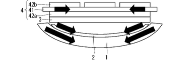
- FIG. 1 is a side view of the warp control structure of the metal base plate according to the embodiment.
- the warp control structure of the metal base plate constitutes a part of the semiconductor module, and includes the metal base plate 1, the dissimilar metal layer 2, and the insulating substrate 4.
- the metal base plate 1 has a square shape in a plan view of about 100 mm ⁇ 100 mm, and has a thickness of 3.5 mmt or more and 4.0 mmt or less. Further, as the material of the metal base plate 1, a high thermal conductive material such as aluminum, an aluminum alloy, or copper is desirable. In this embodiment, aluminum is selected in order to reduce the total weight.
- the dissimilar metal layer 2 is formed only on the entire surface of the metal base plate 1 or only in the region where the insulating substrate 4 is joined on the surface of the metal base plate 1, and has a thickness of about 0.5 mmt.
- the bonding material 3 applied to bond the insulating substrate 4 to the dissimilar metal layer 2 has good wettability, and copper or nickel is preferable. Nickel is selected in this embodiment.
- Examples of the method for forming the dissimilar metal layer 2 include a cold spray method and a metal pasting method.
- the insulating substrate 4 is bonded to the surface of the dissimilar metal layer 2 via a bonding material 3.
- a brazing material, solder, or the like is used as the bonding material 3, but solder is desirable in consideration of manufacturing cost and versatility.
- the thickness of the bonding material 3 which is solder is preferably 0.2 mmt or more and 0.4 mmt or less in consideration of heat dissipation.
- the back surface of the metal base plate 1, which is the surface opposite to the surface on which the dissimilar metal layer 2 is formed, is attached to the cooling fins or the water-cooled jacket via grease. When the metal base plate 1 is attached to the water-cooled jacket, pin fins or straight fins may be formed on the back surface of the metal base plate 1 depending on the refrigerant.
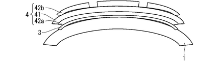
- the insulating substrate 4 has a square shape in a plan view of about 70 mm ⁇ 70 mm, and includes a ceramic substrate 41 and metal plates 42a and 42b.
- a ceramic substrate 41 As the material of the ceramic substrate 41, an appropriate ceramic is selected from ceramics such as alumina, AlN, and Si 3 N 4 according to the application. However, when the warp generated during assembly of the semiconductor module is large (500 ⁇ m or more), it is desirable to select Si 3 N 4 having high bending strength. At that time, the thickness of the ceramic substrate 41 is selected to be 0.32 mmt or 0.64 mmt depending on the withstand voltage with respect to the working voltage.
- the metal plates 42a and 42b are formed on the back surface and the front surface of the ceramic substrate 41, respectively. Further, although aluminum or copper is generally used as the material of the metal plates 42a and 42b, it is desirable that copper is selected in consideration of heat dissipation, and copper is selected in the present embodiment. Further, the thickness of copper is preferably selected in the range of 0.3 mmt or more and 0.8 mmt or less in consideration of heat dissipation and ease of manufacture.
- the materials of the base plate 1, the dissimilar metal layers 2 and the metal plates 42a and 42b are such that the linear expansion coefficient of the metal base plate 1 is ⁇ 1, the linear expansion coefficient of the dissimilar metal layer 2 is ⁇ 2, and the linear expansion coefficients of the metal plates 42a and 42b.
- ⁇ 3 it is selected so as to satisfy ⁇ 1> ⁇ 3> ⁇ 2.
- FIG. 4 is a side view showing a state when the temperature of the metal base plate 1 is changed from room temperature to high temperature in the related technology.
- FIG. 5 is a side view showing a state immediately after the insulating substrate 4 is bonded to the metal base plate 1 in a high temperature state in the related technology.
- FIG. 6 is a side view showing a state when the temperature of the metal base plate 1 and the insulating substrate 4 is changed from high temperature to room temperature in the related technology.
- the dissimilar metal layer 2 is not formed on the surface of the metal base plate 1, and the insulating substrate 4 is bonded to the surface of the metal base plate 1 via the bonding material 3.
- a temperature raising step of raising the temperature of the metal base plate 1 from room temperature to a high temperature is performed. As shown in FIG. 4, the metal base plate 1 does not warp in the temperature raising step and remains flat.
- a joining step of joining the insulating substrate 4 to the surface of the metal base plate 1 via the bonding material 3 is performed in a high temperature state. As shown in FIG. 5, immediately after the joining step, the metal base plate 1 does not warp and remains flat.
- a temperature lowering step is performed in which the temperature of the metal base plate 1 is changed from a high temperature to a room temperature.
- the temperature lowering step as shown by the arrow in FIG. 5, since the linear expansion coefficients of the metal base plate 1 and the insulating substrate 4 are different, the shrinkage amount of the metal base plate 1 and the insulating substrate 4 is different. Therefore, as shown in FIG. 6, in the temperature lowering step after joining, a convex warp occurs on the surface side of the metal base plate 1 to which the insulating substrate 4 is joined.
- the length of the arrow in FIG. 5 indicates the amount of shrinkage between the metal base plate 1 and the insulating substrate 4.
- FIG. 2 is a side view showing a state when the temperature of the metal base plate 1 is changed from room temperature to high temperature in the embodiment.
- FIG. 3 is a side view showing a state immediately after the insulating substrate 4 is bonded to the metal base plate 1 in a high temperature state in the embodiment.
- a temperature raising step of raising the temperature of the metal base plate 1 from room temperature to a high temperature is performed. Since the linear expansion coefficients of the metal base plate 1 and the dissimilar metal layer 2 are different, the expansion amounts of the metal base plate 1 and the dissimilar metal layer 2 are different. As shown in FIG. 2, in the temperature raising step, a convex warp occurs on the side of the metal base plate 1 opposite to the surface to which the insulating substrate 4 is joined.
- the insulating substrate 4 is joined to the surface of the dissimilar metal layer 2 via the bonding material 3 at a high temperature.
- the metal base plate 1 is joined to the insulating substrate 4 in a state of being convexly warped on the side opposite to the surface to which the insulating substrate 4 is bonded. Further, immediately after the joining step, the warp of the metal base plate 1 does not change.
- the metal base plate 1 becomes substantially flat.
- the length of the arrow in FIG. 3 indicates the amount of shrinkage of the metal base plate 1, the dissimilar metal layer 2, and the insulating substrate 4.
- the temperature change from normal temperature (25 ° C.) to high temperature (250 ° C.) and from high temperature (250 ° C.) to normal temperature (25 ° C.) when the dissimilar metal layer 2 is copper or nickel in the present embodiment.
- Table 1 shows the simulation results of warpage due to temperature changes.
- the coefficient of linear expansion of the dissimilar metal layer 2 is the coefficient of linear expansion of the metal plates 42a and 42b as compared with the case where the coefficient of linear expansion of the dissimilar metal layer 2 and the metal plates 42a and 42b are aligned (comparative example). It was found that the warp after joining was reduced when the value was lower than that (in the embodiment).
- the thickness of the metal base plate 1 is 4 mmt
- the thickness of the dissimilar metal layer 2 is 0.5 mmt
- the thicknesses of the metal plates 42a and 42b are 0.4 mmt.
- the semiconductor element is mounted, wired, and case on the bonded body in which the insulating substrate 4 is bonded to the surface of the dissimilar metal layer 2 formed on the metal base plate 1 via the bonding material 3 in a high temperature state.
- the semiconductor module is assembled by attaching and sealing with gel or resin.
- the semiconductor module is cooled by indirect cooling arranged on the cooling fins via grease or the like or direct cooling arranged directly on the water cooling jacket.
- the semiconductor module is incorporated as a component of an inverter device while being arranged on a cooling fin or a water cooling jacket.
- the warp control structure of the metal base plate 1 is joined to the metal base plate 1, the dissimilar metal layer 2 formed on the surface of the metal base plate 1, and the surface of the dissimilar metal layer 2. It is provided with an insulating substrate 4 having metal plates 42a and 42b joined via a material 3 and arranged on both sides, the linear expansion coefficient of the metal base plate 1 is ⁇ 1, and the linear expansion coefficient of the dissimilar metal layer 2 is ⁇ 2.
- the linear expansion coefficient of the metal plates 42a and 42b is ⁇ 3, ⁇ 1> ⁇ 3> ⁇ 2 is satisfied.
- the metal base plate 1 expands with respect to the dissimilar metal layer 2 due to the difference in linear expansion coefficient between the metal base plate 1 and the dissimilar metal layer 2.
- the metal base plate 1 warps convexly on the side opposite to the surface to which the insulating substrate 4 is joined.
- the metal base plates 1 warp in opposite directions, so that the warpage is canceled. This makes it possible to control the warp of the metal base plate 1 that occurs when the temperature changes from high temperature to room temperature.
- the metal base plate 1 is made of aluminum or an aluminum alloy
- the dissimilar metal layer 2 is made of nickel
- the metal plates 42a and 42b are made of copper. Therefore, by adopting an inexpensive aluminum or an aluminum alloy having good thermal conductivity for the metal base plate 1, the heat dissipation of the semiconductor module and the inverter device can be improved. Further, by adopting nickel for the dissimilar metal layer 2, the wettability of the bonding material 3 can be ensured. Further, although aluminum or copper is generally used for the metal plates 42a and 42b, copper is selected from the viewpoint of the coefficient of linear expansion.
- the bonding material 3 is solder, the cost of joining can be reduced by using a highly versatile solder for the bonding material 3. Further, the amount of warpage of the metal base plate 1 that is convexly warped on the side opposite to the surface to which the insulating substrate 4 is bonded due to the temperature change from normal temperature to high temperature, and the temperature change from high temperature to normal temperature after joining the insulating substrate 4
- the amount of warpage convexly on the surface side to which the insulating substrate 4 is joined in the metal base plate 1 does not completely match, and the difference in the amount of warpage increases as the temperature difference between normal temperature and high temperature increases. Therefore, the smaller the temperature difference between normal temperature and high temperature, the more desirable final shape can be obtained in the bonded body.
- the bonding temperature of the solder is 250 ° C. or higher and 300 ° C. or lower, and the temperature difference from the normal temperature is an appropriate temperature, so that a desired final shape can be obtained in the bonded body.
- the semiconductor module includes a warp control structure of a metal base plate and a semiconductor element mounted on the surface of the insulating substrate 4. Therefore, by controlling the warp of the metal base plate 1, the yield of the semiconductor module can be improved.
- the inverter device includes a semiconductor module. Therefore, stable contact between the semiconductor module and the cooling fins or the water-cooled jacket can be performed, so that the yield of the inverter device can be improved.
- 1 metal base plate 1 metal base plate, 2 dissimilar metal layers, 3 bonding materials, 4 insulating substrates, 42a, 42b metal plates.
Abstract
The purpose of the present invention is to provide a technology that controls the warpage of a metal base plate generated while the temperature changes from a high temperature to room temperature, by providing the warpage to the metal base plate in a temperature change from room temperature to the high temperature. . This warpage control structure for a metal base plate 1 comprises a metal base plate 1, a dissimilar metal layer 2, and an insulation substrate 4. The dissimilar metal layer was formed on the surface of the metal base plate 1. The insulation substrate 4 has metal plates 42a, 42b bonded to the surface of the dissimilar metal layer 2 via a bonding material 3 and arranged on both surfaces thereof. When the linear expansion coefficient of the metal base plate 1 is α1, the linear expansion coefficient of the dissimilar metal layer 2 is α2, and the linear expansion coefficient of the metal plates 42a, 42b is α3, α1>α3>α2 is satisfied.
Description
本発明は、金属ベース板に絶縁基板を高温状態で接合する際に発生する反りを制御する技術に関するものである。
The present invention relates to a technique for controlling warpage that occurs when an insulating substrate is joined to a metal base plate in a high temperature state.
半導体モジュールでは、金属ベース板に絶縁基板を接合する構造および方法が採用されている。一般的な接合方法としては、安価なはんだ接合が用いられる場合が多い。ただし、金属ベース板に絶縁基板をはんだ接合した場合、接合後に金属ベース板に反りが発生する。これは、はんだが溶融する際の常温から高温への温度変化では金属ベース板に反りが発生しないが、はんだが凝固する際の高温から常温への温度変化では、金属ベース板と絶縁基板の線膨張係数の差に起因して金属ベース板に大きな反りが発生するためである。このとき、金属ベース板の初期反りがゼロの場合、接合後の反りの向きは、金属ベース板における絶縁基板が接合される面(以下「絶縁基板接合面」ともいう)側に凸の反りとなる。
The semiconductor module employs a structure and method for joining an insulating substrate to a metal base plate. As a general joining method, inexpensive solder joining is often used. However, when the insulating substrate is solder-bonded to the metal base plate, the metal base plate is warped after the bonding. This is because the metal base plate does not warp when the temperature changes from normal temperature to high temperature when the solder melts, but the wire between the metal base plate and the insulating substrate when the temperature changes from high temperature to normal temperature when the solder solidifies. This is because the metal base plate is greatly warped due to the difference in expansion coefficient. At this time, when the initial warp of the metal base plate is zero, the direction of the warp after joining is a warp that is convex toward the surface of the metal base plate to which the insulating substrates are bonded (hereinafter, also referred to as "insulating substrate bonding surface"). Become.
その後、絶縁基板上に半導体素子および電気配線が配置され、半導体モジュールが組み上げられたとき、金属ベース板における絶縁基板接合面とは反対側の面(以下「非接合面」ともいう)の反りが重要となる。金属ベース板の非接合面には、グリスを介して冷却フィンまたは水冷ジャケットが配置されるため、非接合面の反りが半導体モジュールの冷却と密接な関係があるからである。
After that, when the semiconductor element and the electrical wiring are arranged on the insulating substrate and the semiconductor module is assembled, the warp of the surface of the metal base plate opposite to the insulating substrate bonding surface (hereinafter, also referred to as “non-bonding surface”) is generated. It becomes important. This is because the cooling fins or the water-cooled jacket are arranged on the non-bonded surface of the metal base plate via the grease, so that the warp of the non-joined surface is closely related to the cooling of the semiconductor module.
このとき、金属ベース板の絶縁基板接合面側に凸の反りとは反対側への凸反り、すなわち、金属ベース板の非接合面側に凸の反りとなることが望ましい。冷却フィンまたは水冷ジャケットに半導体モジュールが配置される際、半導体モジュールはボルト等で締結されて固定されることが一般的である。金属ベース板の非接合面側に凸であれば、ボルトの軸力で金属ベース板の反りを矯正しつつ、半導体モジュールと冷却フィンまたは水冷ジャケットとの安定した接触を行うことができる。
At this time, it is desirable that the metal base plate has a convex warp on the side opposite to the convex warp on the insulating substrate bonding surface side, that is, a convex warp on the non-bonding surface side of the metal base plate. When the semiconductor module is arranged on the cooling fins or the water-cooled jacket, the semiconductor module is generally fastened and fixed with bolts or the like. If the metal base plate is convex toward the non-joining surface side, the semiconductor module can be stably contacted with the cooling fins or the water-cooled jacket while correcting the warp of the metal base plate by the axial force of the bolt.
金属ベース板の反りを非接合面側に凸とするため、金属ベース板に初期反り付けを付与する反り付け加工を行うことが一般的であるが、金属ベース板の非接合面にフィンなどが存在する場合、反り付け加工を行うことは難しい。
In order to make the warp of the metal base plate convex toward the non-joining surface, it is common to perform a warping process to give the metal base plate an initial warp, but fins or the like are formed on the non-joining surface of the metal base plate. If present, it is difficult to warp.
金属ベース板の反りを制御するために、例えば特許文献1には、金属ベース板の表面に絶縁基板の金属板と同じ種類の金属を貼り付けることで、金属ベース板の反りを低減する方法が開示されている。また、特許文献2には、銅からなる第1の金属層とアルミニウムからなる第2の金属層を含むベースプレートにおいて、第1の金属層と第2の金属層の厚みの比を4:1とすることが開示されている。また、特許文献3には、銅からなる層と酸化銅からなる層を含む銅複合材放熱基板において、銅と酸化銅の比率を変更することで、焼結後の反りを制御する方法が開示されている。
In order to control the warp of the metal base plate, for example, Patent Document 1 describes a method of reducing the warp of the metal base plate by attaching the same type of metal as the metal plate of the insulating substrate to the surface of the metal base plate. It is disclosed. Further, in Patent Document 2, the ratio of the thickness of the first metal layer to the thickness of the second metal layer is set to 4: 1 in the base plate including the first metal layer made of copper and the second metal layer made of aluminum. It is disclosed to do. Further, Patent Document 3 discloses a method of controlling warpage after sintering by changing the ratio of copper and copper oxide in a copper composite heat dissipation substrate including a layer made of copper and a layer made of copper oxide. Has been done.
しかしながら、特許文献1に記載の技術のように、絶縁基板と同じ種類の金属を金属ベース板に貼り付けるだけでは、金属ベース板と貼り付けられた金属における常温から高温への温度変化での反り量よりも、金属ベース板に絶縁基板を高温状態で接合した後の高温から常温への温度変化での反り量が大きくなる。そのため、金属ベース板は絶縁基板接合面側に凸の形状となる。
However, as in the technique described in Patent Document 1, if the same type of metal as the insulating substrate is simply attached to the metal base plate, the metal base plate and the attached metal are warped due to a temperature change from normal temperature to high temperature. The amount of warpage due to the temperature change from high temperature to normal temperature after joining the insulating substrate to the metal base plate in a high temperature state is larger than the amount. Therefore, the metal base plate has a convex shape toward the bonding surface side of the insulating substrate.
特許文献2に記載の技術では、放熱性を向上させるため、剛性の高い銅の厚みが支配的であり、銅よりも剛性の低いアルミニウムの厚みが薄いため、ベースプレートにおける常温から高温への温度変化での反り量が小さくなる。
In the technique described in Patent Document 2, in order to improve heat dissipation, the thickness of copper having high rigidity is dominant, and the thickness of aluminum having lower rigidity than copper is thin, so that the temperature changes from normal temperature to high temperature in the base plate. The amount of warpage at is small.
特許文献3に記載の技術は、高温から常温への温度変化の過程での反りを制御するものであり、銅複合材放熱基板における常温から高温への温度変化での反り量が小さくなる。
The technique described in Patent Document 3 controls warpage in the process of temperature change from high temperature to room temperature, and the amount of warpage in the copper composite heat radiating substrate due to temperature change from room temperature to high temperature is reduced.
そこで、本発明は、常温から高温への温度変化において金属ベース板に反りを付与することで、高温から常温への温度変化において発生する金属ベース板の反りを制御する技術を提供することを目的とする。
Therefore, an object of the present invention is to provide a technique for controlling the warp of a metal base plate generated in a temperature change from a high temperature to a normal temperature by imparting a warp to the metal base plate in a temperature change from a normal temperature to a high temperature. And.
本発明に係る金属ベース板の反り制御構造は、金属ベース板と、前記金属ベース板の表面に形成された異種金属層と、前記異種金属層の表面に接合材を介して接合され、かつ、両面に配置された金属板を有する絶縁基板とを備え、前記金属ベース板の線膨張係数をα1、前記異種金属層の線膨張係数をα2、前記金属板の線膨張係数をα3としたとき、α1>α3>α2を満たすものである。
The warp control structure of the metal base plate according to the present invention is formed by joining the metal base plate, the dissimilar metal layer formed on the surface of the metal base plate, and the surface of the dissimilar metal layer via a bonding material. When an insulating substrate having metal plates arranged on both sides is provided, the linear expansion coefficient of the metal base plate is α1, the linear expansion coefficient of the dissimilar metal layer is α2, and the linear expansion coefficient of the metal plate is α3. It satisfies α1> α3> α2.
本発明によれば、金属ベース板が常温から高温へ温度変化すると、金属ベース板と異種金属層の線膨張係数の差に起因して、異種金属層に対して金属ベース板が膨張し、金属ベース板は絶縁基板が接合される面とは反対側に凸に反る。この状態で、絶縁基板が異種金属層の表面に接合材により接合された後、金属ベース板および絶縁基板が高温から常温へ温度変化すると、絶縁基板と金属ベース板の線膨張係数の差に起因して、絶縁基板に対して金属ベース板が収縮し金属ベース板は絶縁基板が接合される面側に凸に反る。
According to the present invention, when the temperature of the metal base plate changes from normal temperature to high temperature, the metal base plate expands with respect to the dissimilar metal layer due to the difference in linear expansion coefficient between the metal base plate and the dissimilar metal layer, and the metal The base plate warps convexly on the side opposite to the surface to which the insulating substrate is joined. In this state, when the temperature of the metal base plate and the insulating substrate changes from high temperature to room temperature after the insulating substrate is joined to the surface of the dissimilar metal layer with a bonding material, it is caused by the difference in linear expansion coefficient between the insulating substrate and the metal base plate. Then, the metal base plate shrinks with respect to the insulating substrate, and the metal base plate warps convexly toward the surface to which the insulating substrate is joined.
常温から高温への温度変化と高温から常温への温度変化において、金属ベース板は互いに反対方向に反るため、それぞれの反りが打ち消される。これにより、高温から常温への温度変化において発生する金属ベース板の反りを制御することができる。
In the temperature change from normal temperature to high temperature and the temperature change from high temperature to normal temperature, the metal base plates warp in opposite directions, so each warp is canceled. This makes it possible to control the warpage of the metal base plate that occurs when the temperature changes from high temperature to room temperature.
この発明の目的、特徴、局面、および利点は、以下の詳細な説明と添付図面とによって、より明白となる。
The objectives, features, aspects, and advantages of the present invention will be made clearer by the following detailed description and accompanying drawings.
<実施の形態>
本発明の実施の形態について、図面を用いて以下に説明する。図1は、実施の形態に係る金属ベース板の反り制御構造の側面図である。 <Embodiment>
Embodiments of the present invention will be described below with reference to the drawings. FIG. 1 is a side view of the warp control structure of the metal base plate according to the embodiment.
本発明の実施の形態について、図面を用いて以下に説明する。図1は、実施の形態に係る金属ベース板の反り制御構造の側面図である。 <Embodiment>
Embodiments of the present invention will be described below with reference to the drawings. FIG. 1 is a side view of the warp control structure of the metal base plate according to the embodiment.
図1に示すように、金属ベース板の反り制御構造は、半導体モジュールの一部を構成しており、金属ベース板1、異種金属層2、および絶縁基板4を備えている。
As shown in FIG. 1, the warp control structure of the metal base plate constitutes a part of the semiconductor module, and includes the metal base plate 1, the dissimilar metal layer 2, and the insulating substrate 4.
金属ベース板1は約100mm×100mmの平面視にて正方形状であり、厚みは3.5mmt以上4.0mmt以下である。また、金属ベース板1の材質としてはアルミニウム、アルミニウム合金、または銅等の高熱伝導材料が望ましい。本実施の形態では、総重量を軽量化するため、アルミニウムが選択されている。
The metal base plate 1 has a square shape in a plan view of about 100 mm × 100 mm, and has a thickness of 3.5 mmt or more and 4.0 mmt or less. Further, as the material of the metal base plate 1, a high thermal conductive material such as aluminum, an aluminum alloy, or copper is desirable. In this embodiment, aluminum is selected in order to reduce the total weight.
異種金属層2は、金属ベース板1の表面全体または、金属ベース板1の表面における絶縁基板4が接合される領域のみに形成され、厚みは0.5mmt前後である。異種金属層2の材質としては、異種金属層2に絶縁基板4を接合するために塗布される接合材3の濡れ性が良いものが望ましく、銅またはニッケルが望ましい。本実施の形態ではニッケルが選択されている。異種金属層2の形成方法としては、コールドスプレー法または金属貼り付け方法等がある。
The dissimilar metal layer 2 is formed only on the entire surface of the metal base plate 1 or only in the region where the insulating substrate 4 is joined on the surface of the metal base plate 1, and has a thickness of about 0.5 mmt. As the material of the dissimilar metal layer 2, it is desirable that the bonding material 3 applied to bond the insulating substrate 4 to the dissimilar metal layer 2 has good wettability, and copper or nickel is preferable. Nickel is selected in this embodiment. Examples of the method for forming the dissimilar metal layer 2 include a cold spray method and a metal pasting method.
絶縁基板4は、異種金属層2の表面に接合材3を介して接合されている。接合材3としてはろう材またははんだなどが用いられるが、製造コストおよび汎用性を考慮するとはんだが望ましい。はんだである接合材3の厚みは放熱性との兼ね合いで、0.2mmt以上0.4mmt以下が望ましい。金属ベース板1における異種金属層2が形成される面とは逆側の面である裏面は、グリスを介して冷却フィン、または水冷ジャケットに取り付けられる。金属ベース板1が水冷ジャケットに取り付けられる場合は、冷媒に応じて、金属ベース板1の裏面にピンフィンまたはストレートフィンが形成されていてもよい。
The insulating substrate 4 is bonded to the surface of the dissimilar metal layer 2 via a bonding material 3. A brazing material, solder, or the like is used as the bonding material 3, but solder is desirable in consideration of manufacturing cost and versatility. The thickness of the bonding material 3 which is solder is preferably 0.2 mmt or more and 0.4 mmt or less in consideration of heat dissipation. The back surface of the metal base plate 1, which is the surface opposite to the surface on which the dissimilar metal layer 2 is formed, is attached to the cooling fins or the water-cooled jacket via grease. When the metal base plate 1 is attached to the water-cooled jacket, pin fins or straight fins may be formed on the back surface of the metal base plate 1 depending on the refrigerant.
絶縁基板4は約70mm×70mmの平面視にて正方形状であり、セラミック基板41および金属板42a,42bを備えている。セラミック基板41の材質としては、アルミナ、AlN、およびSi3N4等のセラミックから用途に応じて適切なセラミックが選択される。ただし、半導体モジュールの組立時に発生する反りが大きい(500μm以上)場合、抗折強度が高いSi3N4が選択されることが望ましい。その際には、使用電圧に対する耐電圧に応じて、セラミック基板41の厚みは0.32mmtまたは0.64mmtが選択される。
The insulating substrate 4 has a square shape in a plan view of about 70 mm × 70 mm, and includes a ceramic substrate 41 and metal plates 42a and 42b. As the material of the ceramic substrate 41, an appropriate ceramic is selected from ceramics such as alumina, AlN, and Si 3 N 4 according to the application. However, when the warp generated during assembly of the semiconductor module is large (500 μm or more), it is desirable to select Si 3 N 4 having high bending strength. At that time, the thickness of the ceramic substrate 41 is selected to be 0.32 mmt or 0.64 mmt depending on the withstand voltage with respect to the working voltage.
金属板42a,42bは、セラミック基板41の裏面および表面にそれぞれ形成されている。また、金属板42a,42bの材質としてはアルミニウムまたは銅が一般的であるが、放熱性を考慮すると銅が選択されることが望ましく、本実施の形態では銅が選択されている。また、銅の厚みは放熱性および製造しやすさを考慮すると、0.3mmt以上0.8mmt以下の範囲で選択されることが望ましい。
The metal plates 42a and 42b are formed on the back surface and the front surface of the ceramic substrate 41, respectively. Further, although aluminum or copper is generally used as the material of the metal plates 42a and 42b, it is desirable that copper is selected in consideration of heat dissipation, and copper is selected in the present embodiment. Further, the thickness of copper is preferably selected in the range of 0.3 mmt or more and 0.8 mmt or less in consideration of heat dissipation and ease of manufacture.
ここで、常温から高温への温度変化での金属ベース板1の膨張による反り量と、高温から常温への温度変化での金属ベース板1の収縮による反り量を同程度とするために、金属ベース板1、異種金属層2、および金属板42a,42bの材質は、金属ベース板1の線膨張係数をα1、異種金属層2の線膨張係数をα2、金属板42a,42bの線膨張係数をα3としたとき、α1>α3>α2を満たすように選択される。
Here, in order to make the amount of warpage due to the expansion of the metal base plate 1 due to the temperature change from normal temperature to high temperature and the amount of warpage due to the contraction of the metal base plate 1 due to the temperature change from high temperature to normal temperature about the same. The materials of the base plate 1, the dissimilar metal layers 2 and the metal plates 42a and 42b are such that the linear expansion coefficient of the metal base plate 1 is α1, the linear expansion coefficient of the dissimilar metal layer 2 is α2, and the linear expansion coefficients of the metal plates 42a and 42b. When α3, it is selected so as to satisfy α1> α3> α2.
次に、実施の形態に係る金属ベース板の反り制御構造の作用および効果について関連技術の場合と比較しながら説明する。
Next, the action and effect of the warp control structure of the metal base plate according to the embodiment will be described in comparison with the case of the related technology.
最初に関連技術の場合について説明する。図4は、関連技術において、金属ベース板1を常温から高温へ温度変化したときの状態を示す側面図である。図5は、関連技術において、高温状態で金属ベース板1に絶縁基板4が接合された直後の状態を示す側面図である。図6は、関連技術において、金属ベース板1および絶縁基板4を高温から常温へ温度変化したときの状態を示す側面図である。
First, the case of related technology will be explained. FIG. 4 is a side view showing a state when the temperature of the metal base plate 1 is changed from room temperature to high temperature in the related technology. FIG. 5 is a side view showing a state immediately after the insulating substrate 4 is bonded to the metal base plate 1 in a high temperature state in the related technology. FIG. 6 is a side view showing a state when the temperature of the metal base plate 1 and the insulating substrate 4 is changed from high temperature to room temperature in the related technology.
図4と図5に示すように、関連技術では金属ベース板1の表面に異種金属層2が形成されておらず、金属ベース板1の表面に接合材3を介して絶縁基板4が接合される。
As shown in FIGS. 4 and 5, in the related technology, the dissimilar metal layer 2 is not formed on the surface of the metal base plate 1, and the insulating substrate 4 is bonded to the surface of the metal base plate 1 via the bonding material 3. To.
最初に、金属ベース板1の温度を常温から高温にする昇温工程が行われる。図4に示すように、昇温工程では金属ベース板1に反りは発生せず、フラットのままである。
First, a temperature raising step of raising the temperature of the metal base plate 1 from room temperature to a high temperature is performed. As shown in FIG. 4, the metal base plate 1 does not warp in the temperature raising step and remains flat.
次に、高温状態で金属ベース板1の表面に接合材3を介して絶縁基板4を接合する接合工程が行われる。図5に示すように、接合工程の直後では金属ベース板1に反りは発生せず、フラットのままである。
Next, a joining step of joining the insulating substrate 4 to the surface of the metal base plate 1 via the bonding material 3 is performed in a high temperature state. As shown in FIG. 5, immediately after the joining step, the metal base plate 1 does not warp and remains flat.
次に、金属ベース板1の温度を高温から常温にする降温工程が行われる。降温工程では、図5の矢印に示すように、金属ベース板1と絶縁基板4の線膨張係数が異なるため、金属ベース板1と絶縁基板4の収縮量が異なる。そのため、図6に示すように、接合後の降温工程では、金属ベース板1における絶縁基板4が接合される面側に凸の反りが発生する。なお、図5の矢印の長さは、金属ベース板1と絶縁基板4の収縮量を示している。
Next, a temperature lowering step is performed in which the temperature of the metal base plate 1 is changed from a high temperature to a room temperature. In the temperature lowering step, as shown by the arrow in FIG. 5, since the linear expansion coefficients of the metal base plate 1 and the insulating substrate 4 are different, the shrinkage amount of the metal base plate 1 and the insulating substrate 4 is different. Therefore, as shown in FIG. 6, in the temperature lowering step after joining, a convex warp occurs on the surface side of the metal base plate 1 to which the insulating substrate 4 is joined. The length of the arrow in FIG. 5 indicates the amount of shrinkage between the metal base plate 1 and the insulating substrate 4.
次に、実施の形態の場合について説明する。図2は、実施の形態において、金属ベース板1を常温から高温へ温度変化したときの状態を示す側面図である。図3は、実施の形態において、高温状態で金属ベース板1に絶縁基板4が接合された直後の状態を示す側面図である。
Next, the case of the embodiment will be described. FIG. 2 is a side view showing a state when the temperature of the metal base plate 1 is changed from room temperature to high temperature in the embodiment. FIG. 3 is a side view showing a state immediately after the insulating substrate 4 is bonded to the metal base plate 1 in a high temperature state in the embodiment.
最初に、金属ベース板1の温度を常温から高温にする昇温工程が行われる。金属ベース板1と異種金属層2の線膨張係数が異なるため、金属ベース板1と異種金属層2の膨張量が異なる。図2に示すように、昇温工程では、金属ベース板1における絶縁基板4が接合される面とは反対側に凸の反りが発生する。
First, a temperature raising step of raising the temperature of the metal base plate 1 from room temperature to a high temperature is performed. Since the linear expansion coefficients of the metal base plate 1 and the dissimilar metal layer 2 are different, the expansion amounts of the metal base plate 1 and the dissimilar metal layer 2 are different. As shown in FIG. 2, in the temperature raising step, a convex warp occurs on the side of the metal base plate 1 opposite to the surface to which the insulating substrate 4 is joined.
図3に示すように、次に行われる接合工程では高温状態で異種金属層2の表面に接合材3を介して絶縁基板4が接合される。このとき、金属ベース板1は、絶縁基板4が接合される面とは反対側に凸に反った状態で絶縁基板4と接合される。また、接合工程の直後では、金属ベース板1の反りは変化しない。
As shown in FIG. 3, in the next joining step, the insulating substrate 4 is joined to the surface of the dissimilar metal layer 2 via the bonding material 3 at a high temperature. At this time, the metal base plate 1 is joined to the insulating substrate 4 in a state of being convexly warped on the side opposite to the surface to which the insulating substrate 4 is bonded. Further, immediately after the joining step, the warp of the metal base plate 1 does not change.
接合工程後の降温工程では、図3の矢印に示すように、金属ベース板1、異種金属層2、および絶縁基板4の線膨張係数が異なるため、金属ベース板1、異種金属層2、および絶縁基板4の収縮量が異なることから、金属ベース板1における絶縁基板4が接合される面側に凸の反りが発生する。その結果、図1に示すように、金属ベース板1はほぼフラットになる。なお、図3の矢印の長さは、金属ベース板1、異種金属層2、および絶縁基板4の収縮量を示している。
In the temperature lowering step after the joining step, as shown by the arrows in FIG. 3, since the linear expansion coefficients of the metal base plate 1, the dissimilar metal layer 2, and the insulating substrate 4 are different, the metal base plate 1, the dissimilar metal layer 2, and Since the amount of shrinkage of the insulating substrate 4 is different, a convex warp occurs on the surface side of the metal base plate 1 to which the insulating substrate 4 is joined. As a result, as shown in FIG. 1, the metal base plate 1 becomes substantially flat. The length of the arrow in FIG. 3 indicates the amount of shrinkage of the metal base plate 1, the dissimilar metal layer 2, and the insulating substrate 4.
ここで、本実施の形態で異種金属層2を銅またはニッケルとしたときの常温(25℃)から高温(250℃)への温度変化と、高温(250℃)から常温(25℃)への温度変化での反りのシミュレーション結果を表1に示す。表1に示すように、異種金属層2と金属板42a,42bの線膨張係数を揃えた場合(比較例)よりも、異種金属層2の線膨張係数を金属板42a,42bの線膨張係数よりも低くした場合(実施の形態)の方が、接合後の反りが低減することが分かった。
Here, the temperature change from normal temperature (25 ° C.) to high temperature (250 ° C.) and from high temperature (250 ° C.) to normal temperature (25 ° C.) when the dissimilar metal layer 2 is copper or nickel in the present embodiment. Table 1 shows the simulation results of warpage due to temperature changes. As shown in Table 1, the coefficient of linear expansion of the dissimilar metal layer 2 is the coefficient of linear expansion of the metal plates 42a and 42b as compared with the case where the coefficient of linear expansion of the dissimilar metal layer 2 and the metal plates 42a and 42b are aligned (comparative example). It was found that the warp after joining was reduced when the value was lower than that (in the embodiment).

なお、比較例と実施の形態において、金属ベース板1の厚みは4mmt、異種金属層2の厚みは0.5mmt、金属板42a,42bの厚みは0.4mmtである。
In the comparative example and the embodiment, the thickness of the metal base plate 1 is 4 mmt, the thickness of the dissimilar metal layer 2 is 0.5 mmt, and the thicknesses of the metal plates 42a and 42b are 0.4 mmt.
高温状態で、金属ベース板1に形成された異種金属層2の表面に絶縁基板4が接合材3を介して接合された接合体に対して、降温工程後、半導体素子の搭載、配線、ケース付け、およびゲルまたは樹脂封止等が施され、半導体モジュールが組み上がる。半導体モジュールはグリス等を介して冷却フィンに配置される間接冷却または、水冷ジャケットに直接配置される直接冷却により冷却される。半導体モジュールは、冷却フィンまたは水冷ジャケットに配置された状態でインバータ装置の構成部品として組み込まれる。
After the temperature lowering process, the semiconductor element is mounted, wired, and case on the bonded body in which the insulating substrate 4 is bonded to the surface of the dissimilar metal layer 2 formed on the metal base plate 1 via the bonding material 3 in a high temperature state. The semiconductor module is assembled by attaching and sealing with gel or resin. The semiconductor module is cooled by indirect cooling arranged on the cooling fins via grease or the like or direct cooling arranged directly on the water cooling jacket. The semiconductor module is incorporated as a component of an inverter device while being arranged on a cooling fin or a water cooling jacket.
以上のように、実施の形態に係る金属ベース板1の反り制御構造は、金属ベース板1と、金属ベース板1の表面に形成された異種金属層2と、異種金属層2の表面に接合材3を介して接合され、かつ、両面に配置された金属板42a,42bを有する絶縁基板4とを備え、金属ベース板1の線膨張係数をα1、異種金属層2の線膨張係数をα2、金属板42a,42bの線膨張係数をα3としたとき、α1>α3>α2を満たす。
As described above, the warp control structure of the metal base plate 1 according to the embodiment is joined to the metal base plate 1, the dissimilar metal layer 2 formed on the surface of the metal base plate 1, and the surface of the dissimilar metal layer 2. It is provided with an insulating substrate 4 having metal plates 42a and 42b joined via a material 3 and arranged on both sides, the linear expansion coefficient of the metal base plate 1 is α1, and the linear expansion coefficient of the dissimilar metal layer 2 is α2. When the linear expansion coefficient of the metal plates 42a and 42b is α3, α1> α3> α2 is satisfied.
したがって、金属ベース板1が常温から高温へ温度変化すると、金属ベース板1と異種金属層2の線膨張係数の差に起因して、異種金属層2に対して金属ベース板1が膨張し、金属ベース板1は絶縁基板4が接合される面とは反対側に凸に反る。この状態で、絶縁基板4が異種金属層2の表面に接合材3により接合された後、金属ベース板1および絶縁基板4が高温から常温へ温度変化すると、絶縁基板4と金属ベース板1の線膨張係数の差に起因して、絶縁基板4に対して金属ベース板1が収縮し金属ベース板1は絶縁基板4が接合される面側に凸に反る。
Therefore, when the temperature of the metal base plate 1 changes from room temperature to high temperature, the metal base plate 1 expands with respect to the dissimilar metal layer 2 due to the difference in linear expansion coefficient between the metal base plate 1 and the dissimilar metal layer 2. The metal base plate 1 warps convexly on the side opposite to the surface to which the insulating substrate 4 is joined. In this state, after the insulating substrate 4 is bonded to the surface of the dissimilar metal layer 2 by the bonding material 3, when the temperature of the metal base plate 1 and the insulating substrate 4 changes from high temperature to room temperature, the insulating substrate 4 and the metal base plate 1 become Due to the difference in linear expansion coefficient, the metal base plate 1 shrinks with respect to the insulating substrate 4, and the metal base plate 1 warps convexly toward the surface to which the insulating substrate 4 is joined.
常温から高温への温度変化と高温から常温への温度変化において、金属ベース板1は互いに反対方向に反るため、それぞれの反りが打ち消される。これにより、高温から常温への温度変化において発生する金属ベース板1の反りを制御することができる。
In the temperature change from normal temperature to high temperature and the temperature change from high temperature to normal temperature, the metal base plates 1 warp in opposite directions, so that the warpage is canceled. This makes it possible to control the warp of the metal base plate 1 that occurs when the temperature changes from high temperature to room temperature.
金属ベース板1はアルミニウムまたはアルミニウム合金からなり、異種金属層2はニッケルからなり、金属板42a,42bは銅からなる。したがって、金属ベース板1に安価かつ熱伝導率の良いアルミニウムまたはアルミニウム合金を採用することで、半導体モジュールおよびインバータ装置の放熱性を向上させることができる。また、異種金属層2にニッケルを採用することで、接合材3の濡れ性を確保することができる。また、金属板42a,42bにアルミニウムまたは銅を採用することが一般的であるが、線膨張係数の観点から銅が選択される。
The metal base plate 1 is made of aluminum or an aluminum alloy, the dissimilar metal layer 2 is made of nickel, and the metal plates 42a and 42b are made of copper. Therefore, by adopting an inexpensive aluminum or an aluminum alloy having good thermal conductivity for the metal base plate 1, the heat dissipation of the semiconductor module and the inverter device can be improved. Further, by adopting nickel for the dissimilar metal layer 2, the wettability of the bonding material 3 can be ensured. Further, although aluminum or copper is generally used for the metal plates 42a and 42b, copper is selected from the viewpoint of the coefficient of linear expansion.
接合材3ははんだであるため、汎用性の高いはんだを接合材3に採用することで接合にかかる費用が安価になる。また、常温から高温への温度変化での金属ベース板1における絶縁基板4が接合される面とは反対側に凸に反る反り量と、絶縁基板4接合後の高温から常温への温度変化での金属ベース板1における絶縁基板4が接合される面側に凸に反る反り量は完全には一致せず、常温と高温の温度差が大きくなるほど、反り量の差は広がっていく。そのため、常温と高温の温度差が小さいほど、接合体において望ましい最終形状が得られる。はんだの接合温度は250℃以上300℃以下であり、常温との温度差が適当な温度となることから、接合体において望ましい最終形状が得られる。
Since the bonding material 3 is solder, the cost of joining can be reduced by using a highly versatile solder for the bonding material 3. Further, the amount of warpage of the metal base plate 1 that is convexly warped on the side opposite to the surface to which the insulating substrate 4 is bonded due to the temperature change from normal temperature to high temperature, and the temperature change from high temperature to normal temperature after joining the insulating substrate 4 The amount of warpage convexly on the surface side to which the insulating substrate 4 is joined in the metal base plate 1 does not completely match, and the difference in the amount of warpage increases as the temperature difference between normal temperature and high temperature increases. Therefore, the smaller the temperature difference between normal temperature and high temperature, the more desirable final shape can be obtained in the bonded body. The bonding temperature of the solder is 250 ° C. or higher and 300 ° C. or lower, and the temperature difference from the normal temperature is an appropriate temperature, so that a desired final shape can be obtained in the bonded body.
半導体モジュールは、金属ベース板の反り制御構造と、絶縁基板4の表面に実装された半導体素子とを備える。したがって、金属ベース板1の反りを制御することで、半導体モジュールの歩留りを向上させることができる。また、インバータ装置は半導体モジュールを備える。したがって、半導体モジュールと、冷却フィンまたは水冷ジャケットとの安定した接触を行うことができるため、インバータ装置の歩留りを向上させることができる。
The semiconductor module includes a warp control structure of a metal base plate and a semiconductor element mounted on the surface of the insulating substrate 4. Therefore, by controlling the warp of the metal base plate 1, the yield of the semiconductor module can be improved. In addition, the inverter device includes a semiconductor module. Therefore, stable contact between the semiconductor module and the cooling fins or the water-cooled jacket can be performed, so that the yield of the inverter device can be improved.
この発明は詳細に説明されたが、上記した説明は、すべての局面において、例示であって、この発明がそれに限定されるものではない。例示されていない無数の変形例が、この発明の範囲から外れることなく想定され得るものと解される。
Although the present invention has been described in detail, the above description is exemplary in all aspects and the invention is not limited thereto. It is understood that a myriad of variations not illustrated can be envisioned without departing from the scope of the invention.
なお、本発明は、その発明の範囲内において、実施の形態を適宜、変形、省略することが可能である。
In the present invention, the embodiments can be appropriately modified or omitted within the scope of the invention.
1 金属ベース板、2 異種金属層、3 接合材、4 絶縁基板、42a,42b 金属板。
1 metal base plate, 2 dissimilar metal layers, 3 bonding materials, 4 insulating substrates, 42a, 42b metal plates.
Claims (5)
- 金属ベース板と、
前記金属ベース板の表面に形成された異種金属層と、
前記異種金属層の表面に接合材を介して接合され、かつ、両面に配置された金属板を有する絶縁基板と、を備え、
前記金属ベース板の線膨張係数をα1、前記異種金属層の線膨張係数をα2、前記金属板の線膨張係数をα3としたとき、α1>α3>α2を満たす、金属ベース板の反り制御構造。 With a metal base plate
A dissimilar metal layer formed on the surface of the metal base plate and
An insulating substrate that is bonded to the surface of the dissimilar metal layer via a bonding material and has metal plates arranged on both sides thereof.
When the coefficient of linear expansion of the metal base plate is α1, the coefficient of linear expansion of the dissimilar metal layer is α2, and the coefficient of linear expansion of the metal plate is α3, the warp control structure of the metal base plate satisfies α1>α3> α2. .. - 前記金属ベース板はアルミニウムまたはアルミニウム合金からなり、
前記異種金属層はニッケルからなり、
前記金属板は銅からなる、請求項1に記載の金属ベース板の反り制御構造。 The metal base plate is made of aluminum or an aluminum alloy.
The dissimilar metal layer is made of nickel
The warp control structure of the metal base plate according to claim 1, wherein the metal plate is made of copper. - 前記接合材ははんだである、請求項1または請求項2に記載の金属ベース板の反り制御構造。 The warp control structure of the metal base plate according to claim 1 or 2, wherein the bonding material is solder.
- 請求項1から請求項3のいずれか1項に記載の金属ベース板の反り制御構造と、
前記絶縁基板の表面に実装された半導体素子と、
を備える、半導体モジュール。 The warp control structure of the metal base plate according to any one of claims 1 to 3,
The semiconductor element mounted on the surface of the insulating substrate and
A semiconductor module. - 請求項4に記載の半導体モジュールを備える、インバータ装置。 An inverter device including the semiconductor module according to claim 4.
Priority Applications (5)
| Application Number | Priority Date | Filing Date | Title |
|---|---|---|---|
| US17/439,731 US20220157763A1 (en) | 2019-06-06 | 2019-06-06 | Warpage control structure for metal base plate, semiconductor module, and inverter device |
| JP2021524595A JP7154410B2 (en) | 2019-06-06 | 2019-06-06 | Warpage control structure of metal base plate, semiconductor module and inverter device |
| PCT/JP2019/022519 WO2020245975A1 (en) | 2019-06-06 | 2019-06-06 | Warpage control structure for metal base plate, semiconductor module, and inverter device |
| CN201980097064.9A CN113906553A (en) | 2019-06-06 | 2019-06-06 | Warpage control structure of metal base plate, semiconductor module, and inverter device |
| DE112019007396.6T DE112019007396T5 (en) | 2019-06-06 | 2019-06-06 | Warp control structure for metal base plate, semiconductor module and inverter device |
Applications Claiming Priority (1)
| Application Number | Priority Date | Filing Date | Title |
|---|---|---|---|
| PCT/JP2019/022519 WO2020245975A1 (en) | 2019-06-06 | 2019-06-06 | Warpage control structure for metal base plate, semiconductor module, and inverter device |
Publications (1)
| Publication Number | Publication Date |
|---|---|
| WO2020245975A1 true WO2020245975A1 (en) | 2020-12-10 |
Family
ID=73653113
Family Applications (1)
| Application Number | Title | Priority Date | Filing Date |
|---|---|---|---|
| PCT/JP2019/022519 WO2020245975A1 (en) | 2019-06-06 | 2019-06-06 | Warpage control structure for metal base plate, semiconductor module, and inverter device |
Country Status (5)
| Country | Link |
|---|---|
| US (1) | US20220157763A1 (en) |
| JP (1) | JP7154410B2 (en) |
| CN (1) | CN113906553A (en) |
| DE (1) | DE112019007396T5 (en) |
| WO (1) | WO2020245975A1 (en) |
Families Citing this family (1)
| Publication number | Priority date | Publication date | Assignee | Title |
|---|---|---|---|---|
| CN114959701A (en) * | 2022-05-13 | 2022-08-30 | 济南晶正电子科技有限公司 | Composite film, preparation method and electronic component |
Citations (5)
| Publication number | Priority date | Publication date | Assignee | Title |
|---|---|---|---|---|
| JPH1117081A (en) * | 1997-06-19 | 1999-01-22 | Sansha Electric Mfg Co Ltd | Semiconductor module for power |
| JP2002237556A (en) * | 2001-02-09 | 2002-08-23 | Mitsubishi Electric Corp | Power semiconductor device |
| JP2002270748A (en) * | 2001-03-09 | 2002-09-20 | Hitachi Ltd | Semiconductor module and power converter |
| JP2004207619A (en) * | 2002-12-26 | 2004-07-22 | Mitsubishi Materials Corp | Power module and substrate therefor |
| JP2008147308A (en) * | 2006-12-07 | 2008-06-26 | Hitachi Metals Ltd | Circuit board and semiconductor module having same |
Family Cites Families (9)
| Publication number | Priority date | Publication date | Assignee | Title |
|---|---|---|---|---|
| JP2003046032A (en) | 2001-07-26 | 2003-02-14 | Hitachi Ltd | Copper composite material heat-radiating board, semiconductor power module and manufacturing method therefor |
| JP5028147B2 (en) * | 2007-05-29 | 2012-09-19 | 株式会社アライドマテリアル | Heat spreader for semiconductor device and manufacturing method thereof |
| US8519532B2 (en) | 2011-09-12 | 2013-08-27 | Infineon Technologies Ag | Semiconductor device including cladded base plate |
| JP5588956B2 (en) * | 2011-11-30 | 2014-09-10 | 株式会社 日立パワーデバイス | Power semiconductor device |
| CN205752150U (en) | 2013-08-28 | 2016-11-30 | 三菱电机株式会社 | Semiconductor device |
| CN107851617B (en) * | 2015-07-09 | 2021-04-30 | 株式会社东芝 | Ceramic metal circuit board and semiconductor device using the same |
| WO2017086324A1 (en) * | 2015-11-16 | 2017-05-26 | 株式会社豊田中央研究所 | Joining structure and method for manufacturing same |
| JP7031172B2 (en) * | 2017-08-24 | 2022-03-08 | 富士電機株式会社 | Semiconductor device |
| JP7183551B2 (en) * | 2018-03-15 | 2022-12-06 | 富士電機株式会社 | semiconductor equipment |
-
2019
- 2019-06-06 JP JP2021524595A patent/JP7154410B2/en active Active
- 2019-06-06 US US17/439,731 patent/US20220157763A1/en active Pending
- 2019-06-06 WO PCT/JP2019/022519 patent/WO2020245975A1/en active Application Filing
- 2019-06-06 CN CN201980097064.9A patent/CN113906553A/en active Pending
- 2019-06-06 DE DE112019007396.6T patent/DE112019007396T5/en active Pending
Patent Citations (5)
| Publication number | Priority date | Publication date | Assignee | Title |
|---|---|---|---|---|
| JPH1117081A (en) * | 1997-06-19 | 1999-01-22 | Sansha Electric Mfg Co Ltd | Semiconductor module for power |
| JP2002237556A (en) * | 2001-02-09 | 2002-08-23 | Mitsubishi Electric Corp | Power semiconductor device |
| JP2002270748A (en) * | 2001-03-09 | 2002-09-20 | Hitachi Ltd | Semiconductor module and power converter |
| JP2004207619A (en) * | 2002-12-26 | 2004-07-22 | Mitsubishi Materials Corp | Power module and substrate therefor |
| JP2008147308A (en) * | 2006-12-07 | 2008-06-26 | Hitachi Metals Ltd | Circuit board and semiconductor module having same |
Also Published As
| Publication number | Publication date |
|---|---|
| JP7154410B2 (en) | 2022-10-17 |
| DE112019007396T5 (en) | 2022-02-17 |
| US20220157763A1 (en) | 2022-05-19 |
| JPWO2020245975A1 (en) | 2021-10-21 |
| CN113906553A (en) | 2022-01-07 |
Similar Documents
| Publication | Publication Date | Title |
|---|---|---|
| KR102232098B1 (en) | Substrate for heat sink-equipped power module, and production method for same | |
| CN106165090B (en) | Substrate unit for power module and power module | |
| KR101188150B1 (en) | Cooling device | |
| US9786577B2 (en) | Power module substrate, heat-sink-attached power-module substrate, and heat-sink-attached power module | |
| CN108140625B (en) | Substrate for power module with heat sink and power module | |
| WO2016002803A1 (en) | Substrate unit for power modules, and power module | |
| WO2013141110A1 (en) | Method for manufacturing substrate with integrated radiator, and substrate with integrated radiator | |
| EP2306512A2 (en) | Heat radiator and power module | |
| JP6201827B2 (en) | Manufacturing method of power module substrate with heat sink | |
| JP6011552B2 (en) | Power module substrate with heat sink and manufacturing method thereof | |
| JP5164962B2 (en) | Power converter | |
| JP2021132238A (en) | Circuit board and semiconductor module | |
| JP6201828B2 (en) | Manufacturing method of power module substrate with heat sink | |
| WO2019167942A1 (en) | Insulating circuit board | |
| WO2020245975A1 (en) | Warpage control structure for metal base plate, semiconductor module, and inverter device | |
| JP2010199251A (en) | Method of manufacturing semiconductor device | |
| JP6264822B2 (en) | Power module substrate with heat sink and manufacturing method thereof | |
| JP2013211288A (en) | Manufacturing method of substrate for power module with heat sink | |
| JP7054073B2 (en) | Insulated circuit board with heat sink | |
| JP2017011293A (en) | Power module substrate with heat sink and manufacturing method of the same | |
| JP6264889B2 (en) | Power module substrate with heat sink and manufacturing method thereof | |
| JP2021118257A (en) | Insulated circuit board with heat sink, electronic component, and manufacturing method of insulated circuit board with heat sink | |
| JP2002252433A (en) | Ceramic circuit board and its manufacturing method |
Legal Events
| Date | Code | Title | Description |
|---|---|---|---|
| 121 | Ep: the epo has been informed by wipo that ep was designated in this application |
Ref document number: 19931627 Country of ref document: EP Kind code of ref document: A1 |
|
| ENP | Entry into the national phase |
Ref document number: 2021524595 Country of ref document: JP Kind code of ref document: A |
|
| 122 | Ep: pct application non-entry in european phase |
Ref document number: 19931627 Country of ref document: EP Kind code of ref document: A1 |