WO2020245697A1 - 半導体装置 - Google Patents
半導体装置 Download PDFInfo
- Publication number
- WO2020245697A1 WO2020245697A1 PCT/IB2020/054928 IB2020054928W WO2020245697A1 WO 2020245697 A1 WO2020245697 A1 WO 2020245697A1 IB 2020054928 W IB2020054928 W IB 2020054928W WO 2020245697 A1 WO2020245697 A1 WO 2020245697A1
- Authority
- WO
- WIPO (PCT)
- Prior art keywords
- transistor
- circuit
- wiring
- layer
- memory cell
- Prior art date
- Legal status (The legal status is an assumption and is not a legal conclusion. Google has not performed a legal analysis and makes no representation as to the accuracy of the status listed.)
- Ceased
Links
Images








Classifications
-
- G—PHYSICS
- G11—INFORMATION STORAGE
- G11C—STATIC STORES
- G11C11/00—Digital stores characterised by the use of particular electric or magnetic storage elements; Storage elements therefor
- G11C11/21—Digital stores characterised by the use of particular electric or magnetic storage elements; Storage elements therefor using electric elements
- G11C11/34—Digital stores characterised by the use of particular electric or magnetic storage elements; Storage elements therefor using electric elements using semiconductor devices
- G11C11/40—Digital stores characterised by the use of particular electric or magnetic storage elements; Storage elements therefor using electric elements using semiconductor devices using transistors
- G11C11/401—Digital stores characterised by the use of particular electric or magnetic storage elements; Storage elements therefor using electric elements using semiconductor devices using transistors forming cells needing refreshing or charge regeneration, i.e. dynamic cells
- G11C11/4063—Auxiliary circuits, e.g. for addressing, decoding, driving, writing, sensing or timing
- G11C11/407—Auxiliary circuits, e.g. for addressing, decoding, driving, writing, sensing or timing for memory cells of the field-effect type
- G11C11/409—Read-write [R-W] circuits
- G11C11/4097—Bit-line organisation, e.g. bit-line layout, folded bit lines
-
- G—PHYSICS
- G11—INFORMATION STORAGE
- G11C—STATIC STORES
- G11C11/00—Digital stores characterised by the use of particular electric or magnetic storage elements; Storage elements therefor
- G11C11/21—Digital stores characterised by the use of particular electric or magnetic storage elements; Storage elements therefor using electric elements
- G11C11/34—Digital stores characterised by the use of particular electric or magnetic storage elements; Storage elements therefor using electric elements using semiconductor devices
- G11C11/40—Digital stores characterised by the use of particular electric or magnetic storage elements; Storage elements therefor using electric elements using semiconductor devices using transistors
- G11C11/401—Digital stores characterised by the use of particular electric or magnetic storage elements; Storage elements therefor using electric elements using semiconductor devices using transistors forming cells needing refreshing or charge regeneration, i.e. dynamic cells
- G11C11/4063—Auxiliary circuits, e.g. for addressing, decoding, driving, writing, sensing or timing
- G11C11/407—Auxiliary circuits, e.g. for addressing, decoding, driving, writing, sensing or timing for memory cells of the field-effect type
- G11C11/409—Read-write [R-W] circuits
- G11C11/4093—Input/output [I/O] data interface arrangements, e.g. data buffers
-
- G—PHYSICS
- G11—INFORMATION STORAGE
- G11C—STATIC STORES
- G11C11/00—Digital stores characterised by the use of particular electric or magnetic storage elements; Storage elements therefor
- G11C11/21—Digital stores characterised by the use of particular electric or magnetic storage elements; Storage elements therefor using electric elements
- G11C11/34—Digital stores characterised by the use of particular electric or magnetic storage elements; Storage elements therefor using electric elements using semiconductor devices
- G11C11/40—Digital stores characterised by the use of particular electric or magnetic storage elements; Storage elements therefor using electric elements using semiconductor devices using transistors
- G11C11/401—Digital stores characterised by the use of particular electric or magnetic storage elements; Storage elements therefor using electric elements using semiconductor devices using transistors forming cells needing refreshing or charge regeneration, i.e. dynamic cells
- G11C11/4063—Auxiliary circuits, e.g. for addressing, decoding, driving, writing, sensing or timing
- G11C11/407—Auxiliary circuits, e.g. for addressing, decoding, driving, writing, sensing or timing for memory cells of the field-effect type
- G11C11/409—Read-write [R-W] circuits
- G11C11/4094—Bit-line management or control circuits
-
- G—PHYSICS
- G11—INFORMATION STORAGE
- G11C—STATIC STORES
- G11C5/00—Details of stores covered by group G11C11/00
- G11C5/02—Disposition of storage elements, e.g. in the form of a matrix array
- G11C5/04—Supports for storage elements, e.g. memory modules; Mounting or fixing of storage elements on such supports
-
- G—PHYSICS
- G11—INFORMATION STORAGE
- G11C—STATIC STORES
- G11C5/00—Details of stores covered by group G11C11/00
- G11C5/06—Arrangements for interconnecting storage elements electrically, e.g. by wiring
- G11C5/063—Voltage and signal distribution in integrated semi-conductor memory access lines, e.g. word-line, bit-line, cross-over resistance, propagation delay
-
- H—ELECTRICITY
- H10—SEMICONDUCTOR DEVICES; ELECTRIC SOLID-STATE DEVICES NOT OTHERWISE PROVIDED FOR
- H10B—ELECTRONIC MEMORY DEVICES
- H10B12/00—Dynamic random access memory [DRAM] devices
-
- H—ELECTRICITY
- H10—SEMICONDUCTOR DEVICES; ELECTRIC SOLID-STATE DEVICES NOT OTHERWISE PROVIDED FOR
- H10B—ELECTRONIC MEMORY DEVICES
- H10B12/00—Dynamic random access memory [DRAM] devices
- H10B12/30—DRAM devices comprising one-transistor - one-capacitor [1T-1C] memory cells
- H10B12/31—DRAM devices comprising one-transistor - one-capacitor [1T-1C] memory cells having a storage electrode stacked over the transistor
- H10B12/315—DRAM devices comprising one-transistor - one-capacitor [1T-1C] memory cells having a storage electrode stacked over the transistor with the capacitor higher than a bit line
-
- H—ELECTRICITY
- H10—SEMICONDUCTOR DEVICES; ELECTRIC SOLID-STATE DEVICES NOT OTHERWISE PROVIDED FOR
- H10B—ELECTRONIC MEMORY DEVICES
- H10B12/00—Dynamic random access memory [DRAM] devices
- H10B12/50—Peripheral circuit region structures
-
- H—ELECTRICITY
- H10—SEMICONDUCTOR DEVICES; ELECTRIC SOLID-STATE DEVICES NOT OTHERWISE PROVIDED FOR
- H10D—INORGANIC ELECTRIC SEMICONDUCTOR DEVICES
- H10D30/00—Field-effect transistors [FET]
- H10D30/60—Insulated-gate field-effect transistors [IGFET]
- H10D30/67—Thin-film transistors [TFT]
- H10D30/674—Thin-film transistors [TFT] characterised by the active materials
- H10D30/6755—Oxide semiconductors, e.g. zinc oxide, copper aluminium oxide or cadmium stannate
- H10D30/6756—Amorphous oxide semiconductors
-
- H—ELECTRICITY
- H10—SEMICONDUCTOR DEVICES; ELECTRIC SOLID-STATE DEVICES NOT OTHERWISE PROVIDED FOR
- H10D—INORGANIC ELECTRIC SEMICONDUCTOR DEVICES
- H10D64/00—Electrodes of devices having potential barriers
- H10D64/01—Manufacture or treatment
- H10D64/011—Manufacture or treatment of electrodes ohmically coupled to a semiconductor
-
- H—ELECTRICITY
- H10—SEMICONDUCTOR DEVICES; ELECTRIC SOLID-STATE DEVICES NOT OTHERWISE PROVIDED FOR
- H10D—INORGANIC ELECTRIC SEMICONDUCTOR DEVICES
- H10D64/00—Electrodes of devices having potential barriers
- H10D64/20—Electrodes characterised by their shapes, relative sizes or dispositions
- H10D64/27—Electrodes not carrying the current to be rectified, amplified, oscillated or switched, e.g. gates
-
- H—ELECTRICITY
- H10—SEMICONDUCTOR DEVICES; ELECTRIC SOLID-STATE DEVICES NOT OTHERWISE PROVIDED FOR
- H10D—INORGANIC ELECTRIC SEMICONDUCTOR DEVICES
- H10D64/00—Electrodes of devices having potential barriers
- H10D64/60—Electrodes characterised by their materials
- H10D64/66—Electrodes having a conductor capacitively coupled to a semiconductor by an insulator, e.g. MIS electrodes
-
- H—ELECTRICITY
- H10—SEMICONDUCTOR DEVICES; ELECTRIC SOLID-STATE DEVICES NOT OTHERWISE PROVIDED FOR
- H10D—INORGANIC ELECTRIC SEMICONDUCTOR DEVICES
- H10D84/00—Integrated devices formed in or on semiconductor substrates that comprise only semiconducting layers, e.g. on Si wafers or on GaAs-on-Si wafers
-
- H—ELECTRICITY
- H10—SEMICONDUCTOR DEVICES; ELECTRIC SOLID-STATE DEVICES NOT OTHERWISE PROVIDED FOR
- H10D—INORGANIC ELECTRIC SEMICONDUCTOR DEVICES
- H10D84/00—Integrated devices formed in or on semiconductor substrates that comprise only semiconducting layers, e.g. on Si wafers or on GaAs-on-Si wafers
- H10D84/01—Manufacture or treatment
- H10D84/0123—Integrating together multiple components covered by H10D12/00 or H10D30/00, e.g. integrating multiple IGBTs
- H10D84/0126—Integrating together multiple components covered by H10D12/00 or H10D30/00, e.g. integrating multiple IGBTs the components including insulated gates, e.g. IGFETs
-
- H—ELECTRICITY
- H10—SEMICONDUCTOR DEVICES; ELECTRIC SOLID-STATE DEVICES NOT OTHERWISE PROVIDED FOR
- H10D—INORGANIC ELECTRIC SEMICONDUCTOR DEVICES
- H10D84/00—Integrated devices formed in or on semiconductor substrates that comprise only semiconducting layers, e.g. on Si wafers or on GaAs-on-Si wafers
- H10D84/01—Manufacture or treatment
- H10D84/02—Manufacture or treatment characterised by using material-based technologies
- H10D84/03—Manufacture or treatment characterised by using material-based technologies using Group IV technology, e.g. silicon technology or silicon-carbide [SiC] technology
- H10D84/038—Manufacture or treatment characterised by using material-based technologies using Group IV technology, e.g. silicon technology or silicon-carbide [SiC] technology using silicon technology, e.g. SiGe
-
- H—ELECTRICITY
- H10—SEMICONDUCTOR DEVICES; ELECTRIC SOLID-STATE DEVICES NOT OTHERWISE PROVIDED FOR
- H10D—INORGANIC ELECTRIC SEMICONDUCTOR DEVICES
- H10D99/00—Subject matter not provided for in other groups of this subclass
-
- H—ELECTRICITY
- H10—SEMICONDUCTOR DEVICES; ELECTRIC SOLID-STATE DEVICES NOT OTHERWISE PROVIDED FOR
- H10P—GENERIC PROCESSES OR APPARATUS FOR THE MANUFACTURE OR TREATMENT OF DEVICES COVERED BY CLASS H10
- H10P14/00—Formation of materials, e.g. in the shape of layers or pillars
- H10P14/40—Formation of materials, e.g. in the shape of layers or pillars of conductive or resistive materials
-
- H—ELECTRICITY
- H10—SEMICONDUCTOR DEVICES; ELECTRIC SOLID-STATE DEVICES NOT OTHERWISE PROVIDED FOR
- H10W—GENERIC PACKAGES, INTERCONNECTIONS, CONNECTORS OR OTHER CONSTRUCTIONAL DETAILS OF DEVICES COVERED BY CLASS H10
- H10W20/00—Interconnections in chips, wafers or substrates
- H10W20/01—Manufacture or treatment
-
- H—ELECTRICITY
- H10—SEMICONDUCTOR DEVICES; ELECTRIC SOLID-STATE DEVICES NOT OTHERWISE PROVIDED FOR
- H10W—GENERIC PACKAGES, INTERCONNECTIONS, CONNECTORS OR OTHER CONSTRUCTIONAL DETAILS OF DEVICES COVERED BY CLASS H10
- H10W20/00—Interconnections in chips, wafers or substrates
- H10W20/40—Interconnections external to wafers or substrates, e.g. back-end-of-line [BEOL] metallisations or vias connecting to gate electrodes
-
- H—ELECTRICITY
- H10—SEMICONDUCTOR DEVICES; ELECTRIC SOLID-STATE DEVICES NOT OTHERWISE PROVIDED FOR
- H10D—INORGANIC ELECTRIC SEMICONDUCTOR DEVICES
- H10D30/00—Field-effect transistors [FET]
- H10D30/60—Insulated-gate field-effect transistors [IGFET]
- H10D30/67—Thin-film transistors [TFT]
- H10D30/674—Thin-film transistors [TFT] characterised by the active materials
- H10D30/6755—Oxide semiconductors, e.g. zinc oxide, copper aluminium oxide or cadmium stannate
-
- H—ELECTRICITY
- H10—SEMICONDUCTOR DEVICES; ELECTRIC SOLID-STATE DEVICES NOT OTHERWISE PROVIDED FOR
- H10D—INORGANIC ELECTRIC SEMICONDUCTOR DEVICES
- H10D87/00—Integrated devices comprising both bulk components and either SOI or SOS components on the same substrate
-
- H—ELECTRICITY
- H10—SEMICONDUCTOR DEVICES; ELECTRIC SOLID-STATE DEVICES NOT OTHERWISE PROVIDED FOR
- H10W—GENERIC PACKAGES, INTERCONNECTIONS, CONNECTORS OR OTHER CONSTRUCTIONAL DETAILS OF DEVICES COVERED BY CLASS H10
- H10W72/00—Interconnections or connectors in packages
- H10W72/071—Connecting or disconnecting
- H10W72/072—Connecting or disconnecting of bump connectors
- H10W72/07231—Techniques
- H10W72/07236—Soldering or alloying
-
- H—ELECTRICITY
- H10—SEMICONDUCTOR DEVICES; ELECTRIC SOLID-STATE DEVICES NOT OTHERWISE PROVIDED FOR
- H10W—GENERIC PACKAGES, INTERCONNECTIONS, CONNECTORS OR OTHER CONSTRUCTIONAL DETAILS OF DEVICES COVERED BY CLASS H10
- H10W72/00—Interconnections or connectors in packages
- H10W72/20—Bump connectors, e.g. solder bumps or copper pillars; Dummy bumps; Thermal bumps
- H10W72/251—Materials
- H10W72/252—Materials comprising solid metals or solid metalloids, e.g. PbSn, Ag or Cu
-
- H—ELECTRICITY
- H10—SEMICONDUCTOR DEVICES; ELECTRIC SOLID-STATE DEVICES NOT OTHERWISE PROVIDED FOR
- H10W—GENERIC PACKAGES, INTERCONNECTIONS, CONNECTORS OR OTHER CONSTRUCTIONAL DETAILS OF DEVICES COVERED BY CLASS H10
- H10W90/00—Package configurations
-
- H—ELECTRICITY
- H10—SEMICONDUCTOR DEVICES; ELECTRIC SOLID-STATE DEVICES NOT OTHERWISE PROVIDED FOR
- H10W—GENERIC PACKAGES, INTERCONNECTIONS, CONNECTORS OR OTHER CONSTRUCTIONAL DETAILS OF DEVICES COVERED BY CLASS H10
- H10W90/00—Package configurations
- H10W90/20—Configurations of stacked chips
-
- H—ELECTRICITY
- H10—SEMICONDUCTOR DEVICES; ELECTRIC SOLID-STATE DEVICES NOT OTHERWISE PROVIDED FOR
- H10W—GENERIC PACKAGES, INTERCONNECTIONS, CONNECTORS OR OTHER CONSTRUCTIONAL DETAILS OF DEVICES COVERED BY CLASS H10
- H10W90/00—Package configurations
- H10W90/20—Configurations of stacked chips
- H10W90/26—Configurations of stacked chips the stacked chips being of the same size without any chips being laterally offset, e.g. chip stacks having a rectangular shape
-
- H—ELECTRICITY
- H10—SEMICONDUCTOR DEVICES; ELECTRIC SOLID-STATE DEVICES NOT OTHERWISE PROVIDED FOR
- H10W—GENERIC PACKAGES, INTERCONNECTIONS, CONNECTORS OR OTHER CONSTRUCTIONAL DETAILS OF DEVICES COVERED BY CLASS H10
- H10W90/00—Package configurations
- H10W90/20—Configurations of stacked chips
- H10W90/297—Configurations of stacked chips characterised by the through-semiconductor vias [TSVs] in the stacked chips
-
- H—ELECTRICITY
- H10—SEMICONDUCTOR DEVICES; ELECTRIC SOLID-STATE DEVICES NOT OTHERWISE PROVIDED FOR
- H10W—GENERIC PACKAGES, INTERCONNECTIONS, CONNECTORS OR OTHER CONSTRUCTIONAL DETAILS OF DEVICES COVERED BY CLASS H10
- H10W90/00—Package configurations
- H10W90/701—Package configurations characterised by the relative positions of pads or connectors relative to package parts
- H10W90/721—Package configurations characterised by the relative positions of pads or connectors relative to package parts of bump connectors
- H10W90/722—Package configurations characterised by the relative positions of pads or connectors relative to package parts of bump connectors between stacked chips
-
- H—ELECTRICITY
- H10—SEMICONDUCTOR DEVICES; ELECTRIC SOLID-STATE DEVICES NOT OTHERWISE PROVIDED FOR
- H10W—GENERIC PACKAGES, INTERCONNECTIONS, CONNECTORS OR OTHER CONSTRUCTIONAL DETAILS OF DEVICES COVERED BY CLASS H10
- H10W90/00—Package configurations
- H10W90/701—Package configurations characterised by the relative positions of pads or connectors relative to package parts
- H10W90/721—Package configurations characterised by the relative positions of pads or connectors relative to package parts of bump connectors
- H10W90/724—Package configurations characterised by the relative positions of pads or connectors relative to package parts of bump connectors between a chip and a stacked insulating package substrate, interposer or RDL
Definitions
- the semiconductor device is a device that utilizes semiconductor characteristics, and refers to a circuit including a semiconductor element (transistor, diode, photodiode, etc.), a device having the same circuit, and the like. It also refers to all devices that can function by utilizing semiconductor characteristics. For example, an integrated circuit, a chip having an integrated circuit, and an electronic component in which the chip is housed in a package are examples of semiconductor devices. Further, the storage device, the display device, the light emitting device, the lighting device, the electronic device, and the like are themselves semiconductor devices, and may have the semiconductor device.
- IGZO In-Ga-Zn oxides
- Exo In-Ga-Zn oxides
- CAAC c-axis aligned crystalline
- nc nanocrystalline structure
- Oxide semiconductor transistor or "OS transistor”
- OS transistor Oxide semiconductor transistor
- Various semiconductor devices using OS transistors have been manufactured (for example, Non-Patent Documents 3 and 4).
- Patent Document 1 discloses a configuration in which a plurality of layers of a memory cell array having an OS transistor are laminated on a substrate provided with a Si transistor.
- One aspect of the present invention includes a silicon substrate having a first circuit, a first element layer having a second circuit, and a second element layer having a third circuit, and the first circuit is a first transistor.
- the second circuit has a second transistor
- the third circuit has a memory cell
- the memory cell has a third transistor and a capacitor
- the element layer constitutes a laminated block provided by being laminated in a direction perpendicular to or substantially perpendicular to the surface of the silicon substrate, and the laminated block is laminated in a direction perpendicular to or substantially perpendicular to the surface of the silicon substrate.
- a plurality of laminated blocks are provided, and each of the plurality of laminated blocks has a first wiring provided in a direction perpendicular to or substantially perpendicular to the surface of the silicon substrate, and the first wiring is electrically connected to the plurality of laminated blocks. It is a semiconductor device.
- the first circuit has a function of outputting a signal for driving the memory cell and data to be written to the memory cell to the first wiring, and amplifies the data read from the memory cell to the first wiring.
- a semiconductor device having a function is preferable.
- the second circuit has a function of amplifying the potential of the second wiring electrically connected to the memory cell and transmitting the potential to the first wiring, and a function of transmitting the potential of the first wiring to the second wiring.
- a semiconductor device having.
- the second transistor and the third transistor are semiconductor devices each having a semiconductor layer having a metal oxide in a channel forming region.
- the metal oxide preferably contains a semiconductor device containing In, Ga, and Zn.
- the layer having a capacitor is preferably a semiconductor device provided above the layer having a third transistor.
- the layer having a capacitor is preferably a semiconductor device provided in a laminated manner.
- One form of the present invention can provide a semiconductor device or the like having a new configuration.
- one aspect of the present invention can provide a semiconductor device having a novel configuration and the like, which can reduce manufacturing costs in a semiconductor device that functions as a storage device using a minimum off-current.
- one aspect of the present invention can provide a semiconductor device having a novel configuration and excellent low power consumption in a semiconductor device that functions as a storage device using a minimum off-current.
- one aspect of the present invention can provide a semiconductor device having a novel configuration, which can reduce the size of a semiconductor device that functions as a storage device using a minimum off-current.
- one aspect of the present invention can provide a semiconductor device having a novel configuration, which has a small fluctuation in the electrical characteristics of a transistor and is excellent in reliability, in a semiconductor device that functions as a storage device using a minimum off-current. ..
- FIG. 1 is a diagram showing a configuration example of a semiconductor device.
- FIG. 2 is a diagram showing a configuration example of a semiconductor device.
- FIG. 3 is a diagram showing a configuration example of a semiconductor device.
- 4A and 4B are diagrams showing a configuration example of a semiconductor device.
- FIG. 5 is a diagram showing a configuration example of a semiconductor device.
- FIG. 6 is a diagram showing a configuration example of a semiconductor device.
- 7A and 7B are diagrams showing a configuration example of a semiconductor device.
- FIG. 8 is a diagram showing a configuration example of a semiconductor device.
- 9A and 9B are diagrams showing a configuration example of a semiconductor device.
- FIG. 10 is a diagram showing a configuration example of a semiconductor device.
- FIG. 10 is a diagram showing a configuration example of a semiconductor device.
- FIG. 11 is a diagram showing a configuration example of a semiconductor device.
- FIG. 12 is a diagram showing a configuration example of a semiconductor device.
- FIG. 13 is a schematic cross-sectional view showing a configuration example of the semiconductor device.
- FIG. 14 is a schematic cross-sectional view showing a configuration example of the semiconductor device.
- FIG. 15A is a diagram illustrating classification of the crystal structure of IGZO.
- FIG. 15B is a diagram illustrating an XRD spectrum of a CAAC-IGZO film.
- FIG. 15C is a diagram for explaining the microelectron diffraction pattern of the CAAC-IGZO film.
- FIG. 16 is a block diagram illustrating a configuration example of the semiconductor device.
- FIG. 17 is a conceptual diagram showing a configuration example of a semiconductor device.
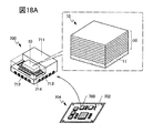
- 18A and 18B are schematic views illustrating an example of an electronic component.
- FIG. 19 is a diagram showing an example of an electronic device.
- the ordinal numbers "1st”, “2nd”, and “3rd” are added to avoid confusion of the components. Therefore, the number of components is not limited. Moreover, the order of the components is not limited. Further, for example, the component referred to in “first” in one of the embodiments of the present specification and the like is defined as a component referred to in “second” in another embodiment or in the claims. It is possible. Further, for example, the component referred to in “first” in one of the embodiments of the present specification and the like may be omitted in another embodiment or in the claims.
- the power supply potential VDD may be abbreviated as potentials VDD, VDD, etc. This also applies to other components (eg, signals, voltages, circuits, elements, electrodes, wiring, etc.).
- the code is used for identification such as "_1”, “_2”, “[n]", “[m, n]”. May be added and described.
- the second wiring GL is described as wiring GL [2].
- a semiconductor device is a device that utilizes semiconductor characteristics, and is a circuit that includes semiconductor elements (transistors, diodes, photodiodes, etc.) and a device that has the same circuit.
- the semiconductor device described in this embodiment can function as a storage device using a transistor having a minimum off-current.
- FIG. 1 is a diagram showing a block diagram of a semiconductor device described in the present embodiment.
- the semiconductor device 10 shown in FIG. 1 has a peripheral circuit 20 provided on a silicon substrate and laminated blocks 30_1 to 30_N (N is a natural number) provided with a plurality of memory cells constituting a memory cell array.
- the laminated blocks 30_1 to 30_N may be collectively referred to as a laminated block 30.
- the configuration applicable to the laminated blocks 30_1 to 30_N may be described as the laminated block 30.
- the silicon substrate refers to a substrate using silicon as a semiconductor material, for example, a single crystal silicon substrate.
- a material having Ge (germanium), SiGe (silicon germanium), GaAs (gallium arsenide), GaAlAs (gallium aluminum arsenide), or the like may be used for the substrate.
- the peripheral circuit 20 includes a circuit for outputting a signal for driving a memory cell such as a row driver and a column driver.
- Row drivers and column drivers may simply be referred to as drive circuits or drivers.
- the row driver and the column driver drive the memory cells at high speed. Therefore, it is preferable that the row driver and the column driver have transistors that operate at high speed.
- the transistor included in the low driver and the column driver is preferably a transistor (Si transistor) having silicon in the channel forming region, which has excellent field effect mobility.
- the low driver is a circuit having a function of outputting a signal for driving a memory cell to a word line.
- the word line has a function of transmitting a word signal to a memory cell.
- the low driver may be called a word line side drive circuit.
- the row driver includes a decoder circuit for selecting a word line corresponding to a designated address, a buffer circuit, and the like.
- the column driver is a circuit having a function of outputting a signal for driving a memory cell to a bit line, a function of outputting data to be written to the memory cell, and a function of amplifying data read from the memory cell to the bit line. ..
- the bit line BL has a function of transmitting data to a memory cell.
- the column driver may be referred to as a bit line side drive circuit.
- the column driver includes a sense amplifier, a precharge circuit, a decoder circuit for selecting a bit line according to a specified address, and the like.
- the data signal given to the bit line corresponds to the signal written in the memory cell or the signal read from the memory cell.
- the data signal will be described as a binary signal with a high or low level potential corresponding to data 1 or data 0.
- the data signal may be a multi-valued data signal having three or more values.
- the high level potential is VDD
- the low level potential is VSS, or ground potential (GND).
- the signal given to the bit line BL includes a data signal, a precharge potential for reading data, and the like.
- the precharge potential can be VDD / 2.
- the laminated blocks 30_1 to 30_N have an element layer 40 and an element layer 50, respectively.
- the element layer 50 has a plurality of memory cells having transistors and capacitors.
- the memory cell included in the element layer 50 can be called a DOSRAM (Dynamic Oxide Semiconductor Random Access Memory) using a transistor having an oxide semiconductor in the channel forming region (hereinafter referred to as an OS transistor) as the memory. Since it can be composed of one transistor and one capacitor, it is possible to realize a high density of memory. Further, by using the OS transistor, the data retention period can be increased.
- DOSRAM Dynamic Oxide Semiconductor Random Access Memory
- the leakage current flowing between the source and the drain at the time of off (hereinafter, off current) is extremely low, which is desired.
- a voltage-dependent charge can be retained in a capacitor on the other side of the source or drain. That is, the data once written can be held in the memory cell for a long time. Therefore, the frequency of data refresh can be reduced and the power consumption can be reduced.
- a memory cell using an OS transistor data can be rewritten and read by charging or discharging an electric charge, so that the number of times of writing and reading data can be substantially unlimited.
- a memory cell using an OS transistor is excellent in rewrite resistance because it does not undergo a structural change at the atomic level unlike a magnetic memory or a resistance change type memory.
- a memory cell using an OS transistor does not show instability due to an increase in electron capture centers even in repeated rewriting operations like a flash memory.
- a memory cell using an OS transistor can be freely arranged on a silicon substrate having a transistor (hereinafter, Si transistor) whose channel forming region has silicon, or an element layer having an OS transistor, so that it can be integrated. It can be done easily. Further, since the OS transistor can be manufactured by using the same manufacturing apparatus as the Si transistor, it can be manufactured at low cost.
- the OS transistor can be a 4-terminal semiconductor element if the back gate electrode is included in addition to the gate electrode, the source electrode and the drain electrode.
- An electric network in which the input and output of signals flowing between the source and the drain can be independently controlled according to the voltage applied to the gate electrode or the back gate electrode can be configured. Therefore, the circuit design can be performed with the same thinking as the LSI.
- the OS transistor has better electrical characteristics than the Si transistor in a high temperature environment. Specifically, since the ratio of the on current to the off current is large even at a high temperature such as 125 ° C. or higher and 150 ° C. or lower, good switching operation can be performed. Further, the OS transistor operates well in the range of ⁇ 40 ° C. or higher and 190 ° C.
- the OS transistor has very good heat resistance.
- This is the heat resistance of the phase change memory (PCM: Phase Change Memory) (-40 ° C or more and 150 ° C or less), and the heat resistance of the resistance change type memory (ReRAM: Resistance Random Access Memory) (-40 ° C or more and 125 ° C or less).
- PCM Phase Change Memory
- ReRAM Resistance Random Access Memory
- the heat resistance is good even when compared with the heat resistance (-40 ° C or higher and 105 ° C or lower) of a magnetic resistance memory (MRAM: Magnetoresistive Random Access Memory).
- the element layer 40 has a function of amplifying the potential of the bit line connected to the memory cell and transmitting it to the bit line connected to the peripheral circuit 20, and a function of transmitting the potential of the peripheral circuit 20 to the bit line connected to the memory cell.
- the bit wire connected to the peripheral circuit 20 is shown as a wiring GBL.
- the bit line connected to the element layer 50 having the memory cell is shown as a wiring LBL.
- the wiring GBL may be referred to as a global bit line.
- the wiring LBL may be referred to as a local bit line.
- the wiring LBL and the wiring GBL have a bit line function for writing or reading data in a memory cell.
- the wiring LBL and the wiring GBL may be shown by a thick line, a thick dotted line, or the like in order to improve visibility.
- the schematic diagram shown in FIG. 1 defines the z-axis direction in order to explain the arrangement of each configuration.
- the z-axis direction may be referred to as a direction perpendicular to the surface of the silicon substrate 11 in the specification.
- the laminated block 30 or the element layer 40 and the element layer 50 constituting the laminated block 30 are laminated in a direction perpendicular to the surface of the silicon substrate 11 or in a substantially vertical direction.
- the term "approximately vertical” means a state in which the objects are arranged at an angle of 85 degrees or more and 95 degrees or less.
- the wiring LBL and the wiring GBL provided on the laminated block 30 are provided in a direction perpendicular to the surface of the silicon substrate 11 or in a substantially vertical direction. With this configuration, the number of memory cells arranged per unit area can be increased, so that the memory density can be increased.
- FIG. 2 is a circuit diagram of a laminated block 30_1 showing a configuration example of a circuit included in the element layer 40 and a configuration example of a memory cell included in the element layer 50.
- the memory cell 51_1 has a transistor 52 and a capacitor 53.
- One of the source and drain of the transistor 52 is connected to the wiring LBL.
- the gate of the transistor 52 is connected to a wiring (also referred to as a word line WL) that gives a word signal.
- the transistor 52 is connected to the capacitor 53.
- the transistor 52 is preferably an OS transistor.
- the OS transistor has an extremely low off current. Therefore, the electric charge corresponding to the data written in the memory cell 51_1 can be held in the capacitor 53 for a long time. That is, in the memory cells 51_1 to 51_N, the once written data can be held for a long time. Therefore, the frequency of data refresh can be reduced, and the power consumption of the semiconductor device according to one aspect of the present invention can be reduced.
- the memory cells 51_1 to 51_N using the OS transistor can be freely arranged on the silicon substrate and the element layer having the OS transistor, integration can be easily performed. Therefore, the number of memory cells arranged per unit area can be increased, and the memory density can be increased.
- the transistor 52 preferably has a back gate electrode. By controlling the potential applied to the back gate electrode, the threshold voltage of the transistor 52 can be controlled. Thereby, for example, the on-current of the transistor 52 can be increased and the off-current can be decreased.
- the element layer 40 shown in FIG. 2 has transistors 41 to 44.
- Each of the transistors 41 to 44 can be composed of an OS transistor, and is shown as an n-channel type transistor.
- the transistor 41 is a transistor for controlling the wiring GBL to a potential corresponding to the potential of the wiring LBL during the period of reading data from the memory cell 51_1.
- the transistor 42 is a transistor that functions as a switch in which a selection signal MUX is input to a gate and on or off between a source and a drain is controlled according to the selection signal MUX.
- the transistor 43 is a transistor that functions as a switch in which a write control signal WE is input to a gate and on or off between a source and a drain is controlled according to the write control signal WE.
- the transistor 44 is a transistor that functions as a switch in which a read control signal RE is input to the gate and on or off between the source and the drain is controlled according to the read control signal RE.
- a ground potential GND which is a fixed potential, is given to the source side of the transistor 44.
- element layer 50 shown in FIG. 2 is shown as a single layer, a plurality of element layers 50 may be laminated. The configuration is illustrated in FIG.
- FIG. 3 is a circuit diagram of a laminated block 30_1 showing a configuration example of a memory cell having element layers 50_1 to 50_p (p is a natural number of 2 or more) as a plurality of element layers 50.
- the element layers 50_1 to 50_p have memory cells 51_1 to 51_p (also referred to as a memory cell 51) connected to a local bit line LBL provided extending in the z-axis direction.
- LBL local bit line
- FIG. 3 shows a configuration in which a plurality of element layers 50_1 to 50_p are stacked as the element layer 50 in the z-axis direction and memory cells are connected by a local bit line LBL provided in the z-axis direction, but as another configuration, May be good.
- FIG. 4A shows, as an example, a configuration in which transistors 41 to 44 included in the element layer 40 and a plurality of element layers 50_1 to 50_4 are provided in four layers in the z-axis direction.
- Each of the element layers 50_1 to 50_1 has a memory cell 51.
- Each memory cell 51 is connected to the gate of the transistor 41 via a local bit line LBL provided in the z-axis direction.
- the element layer 40 has four transistors 41 to 44.
- memory cells are stacked and provided in four element layers as shown in FIG. 4A, four memory cells are provided in each layer of the element layer 40. 16 memory cells can be connected to the gate of the transistor 41 via the local bit line LBL.
- FIG. 4A can be represented as a schematic diagram illustrated in FIG. 4B.
- FIG. 4B illustrates the memory cell 51 included in the element layers 50_1 to 50_1, the local bit line LBL, and the transistor 41 included in the element layer 40.
- the memory cells can be arranged at a high density, but the transistors of the element layer 40 also need to be arranged at a high density.
- the transistor of the element layer 40 is also miniaturized. Since it is necessary to adopt a process having a large number of steps, the manufacturing cost may increase.
- the transistor included in the element layer 40 has a process different from that of the memory cell, that is, a transistor shape capable of reducing the number of steps, rather than a transistor shape having a large number of steps for miniaturization. That is, the transistor included in the element layer 40 is not a transistor shape that prioritizes miniaturization, but a transistor shape that reduces manufacturing costs, for example, a transistor channel length and channel width, that is, a transistor size that is larger than that of a transistor that the memory cell 51 has. By increasing the value, it is possible to suppress an increase in manufacturing cost.
- FIG. 5 is a schematic diagram similar to FIG. 4B, and is a diagram showing a configuration example in which the area occupied by the element layer 40 can be increased.
- the wiring layer 54 has wirings 54_1 and 54_2 connected to the memory cell 51 included in the element layer 50.
- the wiring 54_1 is connected to the gate of the transistor 41_1 included in the element layer 40_1 constituting the element layer 40.
- the wiring 54_2 is connected to the gate of the transistor 41_2 included in the element layer 40_2 constituting the element layer 40.
- the element layer 40_1 and the element have an area occupied by the memory cells 51 provided in the x direction and the y direction.
- the area occupied by the layer 40_2 can be increased. Therefore, the transistor included in the element layer 40 can be formed into a transistor shape that reduces the manufacturing cost instead of a transistor shape that prioritizes miniaturization, so that an increase in the manufacturing cost can be suppressed.
- FIG. 6 is a visualization of the schematic diagram shown in FIG. 5 based on the layout diagram of the memory cells.
- the memory cell 51 has a transistor 52 provided superimposing on the word line WL and a capacitor 53 connected to the transistor 52.
- the configuration in which the wiring layer 54 and the element layer 50 are provided on the element layer 40 is illustrated.
- the wiring 54_1 and the wiring 54_2 are connected to a memory cell provided in the y direction at the openings 57_1 and 57_2.
- the wiring 54_1 and the wiring 54_2 are connected to the element layers 40_1 and 40_2 provided in the y direction at the openings 58_1 and 58_2.
- the element layer 40_1 and the element have an area occupied by the memory cells 51 provided in the x direction and the y direction.
- the area occupied by the layer 40_2 can be increased. Therefore, the transistor included in the element layer 40 can be formed into a transistor shape that reduces the manufacturing cost instead of a transistor shape that prioritizes miniaturization, so that an increase in the manufacturing cost can be suppressed.
- element layer 50_1 shown in FIG. 2 is shown assuming that the transistor and the capacitor are in the same layer, it may be provided in different layers.
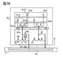
- the configuration is illustrated in FIG. 7B.
- FIG. 7A is a circuit diagram of a laminated block 30_1 showing a configuration example of a memory cell 51_1 having an element layer 50_A as an element layer 50 provided with a transistor 52 and an element layer 50_B as an element layer 50 provided with a capacitor 53.
- the device layer 50_A has a transistor 52
- the device layer 50_B has a capacitor 53.
- the element layer 50_1 shown in FIG. 2 is shown assuming that a plurality of capacitors are provided in the same layer, it may be provided in different layers. The configuration is illustrated in FIG. 7B.
- FIG. 7B shows memory cells 51_A and 51_B having an element layer 50_A as the element layer 50 provided with the transistor 52, an element layer 50_B as the element layer 50 provided with the capacitor 53_A, and an element layer 50_C as the element layer 50 provided with the capacitor 53_B.
- the memory cell 51_A has a transistor 52_A provided in the element layer 50_A and a capacitor 53_A provided in the element layer 50_B.
- the memory cell 51_B has a transistor 52_B provided in the element layer 50_A and a capacitor 53_B provided in the element layer 50_C.
- an IC chip that functions as having the semiconductor device 10
- the semiconductor device 10 can be made into one IC chip by mounting a plurality of dies on a substrate for packaging. 8 and 9A and 9B show an example of the configuration.
- the schematic cross-sectional view of the IC chip 100 illustrated in FIG. 8 has a silicon substrate 11 and a laminated block in which the element layer 40 and the element layers 50_1 to 50_3 are laminated on the package substrate 101.
- the package substrate 101 is provided with a solder ball 102 for connecting the IC chip 100 to a printed circuit board or the like.
- the element layer 40 and the element layers 50_1 to 50_3 can be laminated by repeating the configuration for creating the OS transistor.
- the peripheral circuits provided on the silicon substrate and each circuit such as the memory cell included in the element layer 40 and the element layers 50_1 to 50_3 may be electrically connected via the through electrode 103 provided so as to penetrate each layer. it can.
- TSV Three Silicon Via
- the schematic cross-sectional view of the IC chip 100A shown in FIG. 9A has a silicon substrate 11 and a laminated block in which the element layer 40 and the element layers 50_1 to 50_3 are laminated on the package substrate 101.
- Peripheral circuits provided on the silicon substrate and circuits such as memory cells included in the element layer 40 and the element layers 50_1 to 50_3 are bonded to each other using the silicon substrate 105.
- each layer can be electrically connected via a through electrode 103 provided so as to penetrate each layer and a metal bump 104 provided between the layers.
- the schematic cross-sectional view of the IC chip 100B shown in FIG. 9B has a silicon substrate 11 and a laminated block in which the element layer 40 and the element layers 50_1 to 50_3 are laminated on the package substrate 101.
- Peripheral circuits provided on the silicon substrate and circuits such as memory cells included in the element layer 40 and the element layers 50_1 to 50_3 are bonded to each other using the silicon substrate 105.
- each layer can be electrically connected via a through electrode 103 provided so as to penetrate each layer and a metal bump 104 provided between the layers.
- FIG. 10 is a circuit diagram illustrating a circuit configuration example of the memory cell 51 included in the element layer 50 and a specific circuit configuration example of the peripheral circuit 22 connected to the memory cell described in FIG. ..
- FIG. 10 illustrates the element layers 50_1 to 50_p.
- a memory cell 51_p is illustrated as a memory cell of the element layer 50_p connected to the wiring LBL_A.
- the memory cell 51_p illustrates a transistor 52 and a capacitor 53 whose gate is connected to the word line WL_A.
- a memory cell 51_c is shown as a memory cell of the element layer 50_p connected to the wiring LBL_B.
- the memory cell 51_c illustrates a transistor 52B and a capacitor 53B whose gate is connected to the word line WL_B.
- FIG. 10 illustrates the element layer 40 having the transistors 41_a, 41_b, 42_a, 42_b, 43_a, 43_b, 44_a, 44_b included in the element layer 40.
- the wirings LBL_A and LBL_B are connected to the gates of transistors 41_a and 41_b.
- the transistors 42_a, 42_b, 43_a, 43_b included in the element layer 40 are connected to the wiring GBL_A and GBL_B as shown in FIG.
- the wirings GBL_A and GBL_B are connected to the transistor included in the peripheral circuit 22.
- control signals WE, RE, and MUX are given to the gates of the transistors 42_a, 42_b, 43_a, 43_b, 44_a, and 44_b of the element layer 40.
- FIG. 10 shows a precharge circuit 22_A, a precharge circuit 22_B, a sense amplifier 22_C, a switch circuit 22_D, a switch circuit 22_E, and a write / read circuit 29 on the silicon substrate side as circuits included in the peripheral circuit 22.
- the transistors constituting the precharge circuit 22_A, the precharge circuit 22_B, and the sense amplifier 22_C are composed of Si transistors.
- the switches 23_A to 23_D constituting the switch circuit 22_D and the switch circuit 22_E can also be composed of Si transistors.
- One of the source or drain of the transistors 42_a, 42_b, 43_a, 43_b is connected to the transistors constituting the precharge circuit 22_A, the precharge circuit 22_B, the sense amplifier 22_C, and the switch circuit 22_D.
- the precharge circuit 22_A is composed of n-channel type transistors 24_1 to 24_3.
- the precharge circuit 22_A is a circuit for precharging the wirings LBL_A and LBL_B to the intermediate potential VPC corresponding to the potential VDD / 2 between VDD and VSS according to the precharge signal given to the precharge line PCL1. ..
- the precharge circuit 22_B is composed of n-channel type transistors 24_4 to 24_6.
- the precharge circuit 22_B is a circuit for precharging the wiring GBL_A and the wiring GBL_B to the intermediate potential VPC corresponding to the potential VDD / 2 between VDD and VSS according to the precharge signal given to the precharge line PCL2. is there.
- the sense amplifier 22_C is composed of p-channel transistors 25_1 and 25_2 and n-channel transistors 25_3 and 25_4 connected to the wiring VHH or wiring VLL.
- Wiring VHH or Wiring VLL is a wiring having a function of giving VDD or VSS.
- Transistors 25_1 to 25_1 are transistors that form an inverter loop.
- the potentials of the wiring GBL_A and the wiring GBL_B can be output to the outside via the write / read circuit 29 via the switch circuit 22_D and the switch circuit 22_E.
- the wiring LBL_A and LBL_B, and the wiring GBL_A and wiring GBL_B correspond to a bit line pair.
- the write / read circuit 25 controls the writing of the data signal according to the signal EN_data.
- the switch circuit 22_D is a circuit for controlling the conduction state between the sense amplifier 22_C and the wiring GBL_A and the wiring GBL_B.
- the switch circuit 22_D is switched on or off by controlling the switching signal CSEL1.
- the switches 23_A and 23_B are n-channel transistors, the switching signal CSEL1 is turned on at a high level and turned off at a low level.
- the switch circuit 22_E is a circuit for controlling the conduction state between the write / read circuit 29 and the bit line pair connected to the sense amplifier 22_C.
- the switch circuit 22_D is switched on or off by controlling the switching signal CSEL1.
- the switches 23_C and 23_D may be the same as the switches 23_A and 23_B.
- FIG. 11 shows a timing chart for explaining the operation of the circuit diagram shown in FIG.
- the period T11 is the write operation
- the period T12 is the wiring LBL precharge operation
- the period T13 is the wiring GBL precharge operation
- the period T14 is the charge sharing operation
- the period T15 is the read standby.
- the operation, period T16 corresponds to the period for explaining the read operation.
- the word line connected to the gate of the transistor of the memory cell in which the data signal is to be written is set to the high level.
- the control signal WE and the signal EN_data are set to a high level, and the data signal is written to the memory cell via the wiring GBL and the bit line BL.
- the precharge line PCL1 is set to a high level while the control signal WE is set to a high level.
- the bit line BL is precharged to the precharge potential.
- both the wiring VHH and the wiring VLL that supply the power supply voltage to the sense amplifier 22_C are set to VDD / 2 to suppress the power consumption due to the through current.
- the precharge line PCL2 is set to a high level in order to precharge the wiring GBL.
- the wiring GBL is precharged to the precharge potential.
- control signal WL and the control signal MUX are set to high levels for charge sharing for balancing the charges precharged in the bit line BL and the wiring GBL.
- the bit wire BL and the wiring GBL are equipotential.
- both the wiring VHH and the wiring VLL that supply the power supply voltage to the sense amplifier 22_C are set to VDD / 2 to suppress the power consumption due to the through current.
- the control signal RE is set to a high level. This is a period in which a current flows through the transistor 41 according to the potential of the bit line BL and the potential of the wiring GBL fluctuates according to the amount of the current.
- the switching signal CSEL1 is set to a low level so that the fluctuation of the potential of the wiring GBL is not affected by the sense amplifier 22_C.
- Wiring VHH or wiring VLL is similar to period T14.
- the data signal written in the memory cell is read out by amplifying the fluctuation of the potential of the wiring GBL with the bit line pair connected to the sense amplifier 22_C with the switching signal CSEL1 as the high level.
- One form of the semiconductor device of the present invention uses an OS transistor having an extremely low off-current as a transistor provided in each element layer.
- the OS transistor can be laminated on a silicon substrate on which a Si transistor is provided. Therefore, it can be manufactured by repeating the same manufacturing process in the vertical direction, and the manufacturing cost can be reduced. Further, in one embodiment of the present invention, the transistors constituting the memory cell can be arranged in the vertical direction instead of the plane direction to improve the memory density, and the device can be miniaturized.
- the wiring LBL is connected to the gate of the transistor 41, data can be read out using a slight potential difference of the wiring LBL. Since a circuit such as a sense amplifier using a Si transistor can be miniaturized, the semiconductor device can be miniaturized. Further, it can be operated even if the capacity of the capacitor of the memory cell is reduced.
- One embodiment of the present invention uses an OS transistor having an extremely low off-current as a transistor provided in each element layer. Therefore, the frequency of refreshing the data held in the memory cell can be reduced, and the semiconductor device can be made with low power consumption.
- the OS transistors can be stacked and provided, and can be manufactured by repeating the same manufacturing process in the vertical direction, so that the manufacturing cost can be reduced. Further, in one embodiment of the present invention, the transistors constituting the memory cell can be arranged in the vertical direction instead of the plane direction to improve the memory density, and the device can be miniaturized.
- the OS transistor since the OS transistor has less fluctuation in electrical characteristics than the Si transistor even in a high temperature environment, the fluctuation in electrical characteristics of the transistor when stacked and integrated is small, and the semiconductor device functions as a highly reliable storage device. Can be.
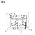
- the transistor is shown as a transistor having a top gate structure or a bottom gate structure without a back gate electrode, but the structure of the transistor 52 is not limited to this.
- the transistor included in the memory cell 51 may be a transistor 52 having a back gate electrode connected to the back gate electrode line BGL. With the configuration shown in FIG. 12, it is possible to make it easier to control electrical characteristics such as the threshold voltage of the transistor 52 from the outside.
- FIG. 13 shows a memory unit 470 (memory unit 470_1 to memory unit 470_m: m is a natural number of 2 or more) on the element layer 411 having a circuit provided on the semiconductor substrate 311.
- (Shown) is a diagram showing an example of a semiconductor device provided in a laminated manner.
- a plurality of memory units 470 are laminated on the element layer 411 and the element layer 411.
- the plurality of memory units 470 include a transistor layer 413 (transistor layer 413_1 to transistor layer 413_m) corresponding to each memory unit 470 on the substrate 450, and a plurality of memory device layers 415 (memory device layer) on each transistor layer 413.
- n are natural numbers of 2 or more).
- the transistor layer 413 is provided on the substrate 450 and the memory device layer 415 is provided on the transistor layer 413 is shown, but the present embodiment is not limited to this.
- a plurality of memory device layers 415 may be provided on the substrate 450, and a transistor layer 413 may be provided on the plurality of memory device layers 415, or memory device layers 415 may be provided above and below the transistor layer 413 on the substrate 450. You may.
- a material selected from Si, Ge, SiGe, GaAs, GaAlAs, GaN, and InP can be used, respectively.
- the element layer 411 has a transistor 300 provided on the semiconductor substrate 311 and can function as a circuit of a semiconductor device (sometimes called a peripheral circuit).
- Examples of circuits include column drivers, row drivers, column decoders, row decoders, sense amplifiers, precharge circuits, amplifier circuits, word line driver circuits, output circuits, control logic circuits, and the like.
- the transistor layer 413 has a transistor 200T and can function as a circuit for controlling each memory unit 470.
- the memory device layer 415 has a memory device 420.
- the memory device 420 shown in this embodiment has a transistor and a capacitance.
- m is not particularly limited, but is 2 or more and 100 or less, preferably 2 or more and 50 or less, and more preferably 2 or more and 10 or less.
- n is not particularly limited, but is 2 or more and 100 or less, preferably 2 or more and 50 or less, and more preferably 2 or more and 10 or less.
- the product of m and n is 4 or more and 256 or less, preferably 4 or more and 128 or less, and more preferably 4 or more and 64 or less.
- FIG. 13 shows a cross-sectional view of the transistor 200T included in the memory unit and the transistor included in the memory device 420 in the channel length direction.
- a transistor 300 is provided on the semiconductor substrate 311, and a transistor layer 413 and a memory device layer 415 of the memory unit 470 are provided on the transistor 300, and the transistor layer 413 is provided in one memory unit 470.
- the transistor 200T included in the memory device layer 415 and the memory device 420 included in the memory device layer 415 are electrically connected by a plurality of conductors 424, and the transistor 300 and the transistor 200T included in the transistor layer 413 in each memory unit 470 are connected to the transistor 426.
- Conductor 427, and conductor 430 are electrically connected.
- the conductor 426 is electrically connected to the transistor 200T via a conductor 428 which is electrically connected to any one of the source, drain and gate of the transistor 200T.
- the conductor 424 is preferably provided in each layer of the memory device layer 415.
- the conductor 427 is provided on the uppermost layer of each memory unit 470 and is electrically connected to the conductor 426 and the conductor 430.
- a material selected from Cu, W, Ti, Ta, and Al can be used, respectively.
- FIG. 13 shows an example in which the substrate 450 of the memory unit 470 is provided on the transistor 300 side, but the present embodiment is not limited to this.
- the memory unit 470 may be provided so that the memory device layer 415 is provided on the transistor 300 side.
- the conductor 426 is provided so as to penetrate the memory device layer 415
- the conductor 430 is provided so as to penetrate the memory device layer 415, the transistor layer 413, and the substrate 450.
- the conductor 426 is provided so as to penetrate the substrate 450 and the transistor layer 413
- the conductor 430 is provided so as to penetrate the substrate 450, the transistor layer 413, and the memory device layer 415. ..
- an insulator such as water or hydrogen or an insulator that suppresses the permeation of oxygen on the side surface of the conductor 424 and the side surface of the conductor 426.
- an insulator for example, silicon nitride, aluminum oxide, silicon nitride or the like may be used.
- the memory device 420 has a transistor and a capacitance on the side surface thereof, and the transistor can have a structure similar to that of the transistor 200T included in the transistor layer 413.
- the transistor 200T uses a metal oxide (hereinafter, also referred to as an oxide semiconductor) that functions as an oxide semiconductor as a semiconductor that includes a region in which a channel is formed (hereinafter, also referred to as a channel formation region). Is preferable.
- an oxide semiconductor that functions as an oxide semiconductor as a semiconductor that includes a region in which a channel is formed (hereinafter, also referred to as a channel formation region). Is preferable.
- oxide semiconductors for example, In-M-Zn oxide (element M is aluminum, gallium, yttrium, tin, copper, vanadium, beryllium, boron, titanium, iron, nickel, germanium, zirconium, molybdenum, lantern, cerium). , Neodymium, hafnium, tantalum, tungsten, magnesium, etc. (one or more) and the like may be used. Further, as the oxide semiconductor, indium oxide, In—Ga oxide, or In—Zn oxide may be used. By using an oxide semiconductor having a composition having a high proportion of indium, it is possible to increase the on-current of the transistor, the mobility of the field effect, and the like.
- the transistor 200T using an oxide semiconductor in the channel formation region has an extremely small leakage current in a non-conducting state, it is possible to provide a semiconductor device with low power consumption. Further, since the oxide semiconductor can be formed into a film by a sputtering method or the like, it can be used for a transistor 200T constituting a highly integrated semiconductor device.
- a transistor including an oxide semiconductor, impurities and oxygen vacancies in the oxide semiconductor by (V O oxygen vacancy also called), its electrical characteristics are varied, a voltage is applied to normally on (gate electrode Even if there is no channel, there is a characteristic that current flows through the transistor).
- a low impurity concentration and a low defect level density is referred to as high-purity intrinsic or substantially high-purity intrinsic.
- impurity concentration in the oxide semiconductor is reduced as much as possible.
- impurities in the oxide semiconductor include hydrogen, nitrogen, alkali metal, alkaline earth metal, iron, nickel, silicon and the like.
- hydrogen as an impurity contained in the oxide semiconductor may form an oxygen deficiency in the oxide semiconductor.
- defects containing hydrogen to an oxygen vacancy (hereinafter may be referred to as V O H.) May generate electrons serving as carriers.
- a part of hydrogen may react with oxygen bonded to a metal atom to generate an electron as a carrier.
- a transistor using an oxide semiconductor containing a large amount of hydrogen tends to have normal-on characteristics. Further, since hydrogen in the oxide semiconductor easily moves due to stress such as heat and electric field, if the oxide semiconductor contains a large amount of hydrogen, the reliability of the transistor may deteriorate.
- the oxide semiconductor used for the transistor 200T it is preferable to use a high-purity intrinsic oxide semiconductor in which impurities such as hydrogen and oxygen deficiency are reduced.
- the metal oxide preferably contains at least indium or zinc. In particular, it preferably contains indium and zinc. In addition to them, it is preferable that one or a plurality of types selected from aluminum, gallium, yttrium, and tin are contained. Further, one or more kinds selected from boron, titanium, iron, nickel, germanium, zirconium, molybdenum, lantern, cerium, neodymium, hafnium, tantalum, tungsten, magnesium, cobalt and the like may be contained. For example, a metal oxide having indium, zinc, and gallium (In-Ga-Zn-based oxide), and a metal oxide having indium, zinc, and tin (In-Sn-Zn-based oxide). ), Or a metal oxide (In-Ga-Zn-Sn-based oxide) having indium, zinc, gallium, and tin can be preferably used.
- FIG. 15A is a diagram illustrating classification of crystal structures of oxide semiconductors, typically IGZO (metal oxides containing In, Ga, and Zn).
- IGZO metal oxides containing In, Ga, and Zn
- oxide semiconductors are roughly classified into “Amorphous (amorphous)”, “Crystalline (crystallinity)", and “Crystal (crystal)”.
- Amorphous includes “completable amorphous”.
- the "Crystalline” includes CAAC (c-axis-aligned crystalline), nc (nanocrystalline), and CAC (cloud-aligned crystal) (extracting single crystal crystal).
- single crystal, poly crystal, and single crystal amorphous are excluded from the classification of "Crystalline”.
- “Crystal” includes single crystal and poly crystal.
- the structure in the thick frame shown in FIG. 15A is an intermediate state between "Amorphous” and “Crystal", and belongs to a new boundary region (New crystal line phase). .. That is, the structure can be rephrased as a structure completely different from the energetically unstable "Amorphous” and "Crystal".
- the crystal structure of the film or substrate can be evaluated using an X-ray diffraction (XRD: X-Ray Evaluation) spectrum.
- XRD X-ray diffraction
- FIG. 15B the XRD spectrum obtained by GIXD (Glazing-Incidence XRD) measurement of the CAAC-IGZO film classified as "Crystalline" is shown in FIG. 15B (the vertical axis represents the intensity (Intensity) as an arbitrary unit (a.u.)). (Represented by).
- the GIXD method is also referred to as a thin film method or a Seemann-Bohlin method.
- the XRD spectrum obtained by the GIXD measurement shown in FIG. 15B will be simply referred to as an XRD spectrum.
- a peak showing clear crystallinity is detected in the XRD spectrum of the CAAC-IGZO film.
- the crystal structure of the film or the substrate can be evaluated by a diffraction pattern (also referred to as a microelectron diffraction pattern) observed by a micro electron diffraction method (NBED: Nano Beam Electron Diffraction).
- the diffraction pattern of the CAAC-IGZO film is shown in FIG. 15C.
- FIG. 15C is a diffraction pattern observed by the NBED in which the electron beam is incident parallel to the substrate.
- electron beam diffraction is performed with the probe diameter set to 1 nm.
- oxide semiconductors may be classified differently from FIG. 15A.
- oxide semiconductors are divided into single crystal oxide semiconductors and other non-single crystal oxide semiconductors.
- the non-single crystal oxide semiconductor include the above-mentioned CAAC-OS and nc-OS.
- the non-single crystal oxide semiconductor includes a polycrystalline oxide semiconductor, a pseudo-amorphous oxide semiconductor (a-like OS: amorphous-like oxide semiconductor), an amorphous oxide semiconductor, and the like.
- CAAC-OS CAAC-OS
- nc-OS nc-OS
- a-like OS the details of the above-mentioned CAAC-OS, nc-OS, and a-like OS will be described.
- CAAC-OS is an oxide semiconductor having a plurality of crystal regions, the plurality of crystal regions having the c-axis oriented in a specific direction.
- the specific direction is the thickness direction of the CAAC-OS film, the normal direction of the surface to be formed of the CAAC-OS film, or the normal direction of the surface of the CAAC-OS film.
- the crystal region is a region having periodicity in the atomic arrangement. When the atomic arrangement is regarded as a lattice arrangement, the crystal region is also a region in which the lattice arrangement is aligned. Further, the CAAC-OS has a region in which a plurality of crystal regions are connected in the ab plane direction, and the region may have distortion.
- the strain refers to a region in which a plurality of crystal regions are connected in which the orientation of the lattice arrangement changes between a region in which the lattice arrangement is aligned and a region in which another grid arrangement is aligned.
- CAAC-OS is an oxide semiconductor that is c-axis oriented and not clearly oriented in the ab plane direction.
- Each of the plurality of crystal regions is composed of one or a plurality of minute crystals (crystals having a maximum diameter of less than 10 nm).
- the maximum diameter of the crystal region is less than 10 nm.
- the size of the crystal region may be about several tens of nm.
- CAAC-OS has indium (In) and oxygen. It tends to have a layered crystal structure (also referred to as a layered structure) in which a layer (hereinafter, In layer) and a layer having elements M, zinc (Zn), and oxygen (hereinafter, (M, Zn) layer) are laminated. There is. Indium and element M can be replaced with each other. Therefore, the (M, Zn) layer may contain indium. In addition, the In layer may contain the element M. In addition, Zn may be contained in the In layer.
- the layered structure is observed as a lattice image in, for example, a high-resolution TEM image.
- the position of the peak indicating the c-axis orientation may vary depending on the type and composition of the metal elements constituting CAAC-OS.
- a plurality of bright spots are observed in the electron diffraction pattern of the CAAC-OS film. Note that a certain spot and another spot are observed at point-symmetrical positions with the spot of the incident electron beam passing through the sample (also referred to as a direct spot) as the center of symmetry.
- the lattice arrangement in the crystal region is based on a hexagonal lattice, but the unit lattice is not limited to a regular hexagon and may be a non-regular hexagon. Further, in the above strain, it may have a lattice arrangement such as a pentagon or a heptagon.
- a clear grain boundary cannot be confirmed even in the vicinity of strain. That is, it can be seen that the formation of grain boundaries is suppressed by the distortion of the lattice arrangement. This is because CAAC-OS can tolerate distortion because the arrangement of oxygen atoms is not dense in the ab plane direction and the bond distance between atoms changes due to substitution of metal atoms. It is thought that this is the reason.
- CAAC-OS for which no clear crystal grain boundary is confirmed, is one of the crystalline oxides having a crystal structure suitable for the semiconductor layer of the transistor.
- a configuration having Zn is preferable.
- In-Zn oxide and In-Ga-Zn oxide are more suitable than In oxide because they can suppress the generation of grain boundaries.
- CAAC-OS is an oxide semiconductor with high crystallinity and no clear grain boundaries can be confirmed. Therefore, it can be said that CAAC-OS is unlikely to cause a decrease in electron mobility due to grain boundaries. Further, since the crystallinity of the oxide semiconductor may be lowered due to the mixing of impurities or the generation of defects, CAAC-OS can be said to be an oxide semiconductor having few impurities and defects (oxygen deficiency, etc.). Therefore, the oxide semiconductor having CAAC-OS has stable physical properties. Therefore, the oxide semiconductor having CAAC-OS is resistant to heat and has high reliability. CAAC-OS is also stable against high temperatures in the manufacturing process (so-called thermal budget). Therefore, if CAAC-OS is used for the OS transistor, the degree of freedom in the manufacturing process can be expanded.
- nc-OS has periodicity in the atomic arrangement in a minute region (for example, a region of 1 nm or more and 10 nm or less, particularly a region of 1 nm or more and 3 nm or less).
- nc-OS has tiny crystals. Since the size of the minute crystal is, for example, 1 nm or more and 10 nm or less, particularly 1 nm or more and 3 nm or less, the minute crystal is also referred to as a nanocrystal.
- nc-OS does not show regularity in crystal orientation between different nanocrystals. Therefore, no orientation is observed in the entire film.
- the nc-OS may be indistinguishable from the a-like OS and the amorphous oxide semiconductor depending on the analysis method.
- a peak indicating crystallinity is not detected in the Out-of-plane XRD measurement using a ⁇ / 2 ⁇ scan.
- electron beam diffraction also referred to as limited field electron diffraction
- a diffraction pattern such as a halo pattern is performed. Is observed.
- electron diffraction also referred to as nanobeam electron diffraction
- an electron beam having a probe diameter for example, 1 nm or more and 30 nm or less
- An electron diffraction pattern in which a plurality of spots are observed in a ring-shaped region centered on a direct spot may be acquired.
- the a-like OS is an oxide semiconductor having a structure between nc-OS and an amorphous oxide semiconductor.
- the a-like OS has a void or low density region. That is, the a-like OS has lower crystallinity than the nc-OS and CAAC-OS.
- a-like OS has a higher hydrogen concentration in the membrane than nc-OS and CAAC-OS.
- CAC-OS relates to the material composition.
- CAC-OS is, for example, a composition of a material in which the elements constituting the metal oxide are unevenly distributed in a size of 0.5 nm or more and 10 nm or less, preferably 1 nm or more and 3 nm or less, or a size close thereto.
- the metal oxide one or more metal elements are unevenly distributed, and the region having the metal element has a size of 0.5 nm or more and 10 nm or less, preferably 1 nm or more and 3 nm or less, or a size close thereto.
- the mixed state is also called a mosaic shape or a patch shape.
- CAC-OS has a structure in which the material is separated into a first region and a second region to form a mosaic shape, and the first region is distributed in the membrane (hereinafter, also referred to as a cloud shape). It says.). That is, CAC-OS is a composite metal oxide having a structure in which the first region and the second region are mixed.
- the atomic number ratios of In, Ga, and Zn with respect to the metal elements constituting CAC-OS in the In-Ga-Zn oxide are expressed as [In], [Ga], and [Zn], respectively.
- the first region is a region in which [In] is larger than [In] in the composition of the CAC-OS film.
- the second region is a region in which [Ga] is larger than [Ga] in the composition of the CAC-OS film.
- the first region is a region in which [In] is larger than [In] in the second region and [Ga] is smaller than [Ga] in the second region.
- the second region is a region in which [Ga] is larger than [Ga] in the first region and [In] is smaller than [In] in the first region.
- the first region is a region in which indium oxide, indium zinc oxide, or the like is the main component.
- the second region is a region in which gallium oxide, gallium zinc oxide, or the like is the main component. That is, the first region can be rephrased as a region containing In as a main component. Further, the second region can be rephrased as a region containing Ga as a main component.
- a region containing In as a main component (No. 1) by EDX mapping acquired by using energy dispersive X-ray spectroscopy (EDX: Energy Dispersive X-ray spectroscopy). It can be confirmed that the region (1 region) and the region containing Ga as a main component (second region) have a structure in which they are unevenly distributed and mixed.
- EDX Energy Dispersive X-ray spectroscopy
- CAC-OS When CAC-OS is used for a transistor, the conductivity caused by the first region and the insulating property caused by the second region act in a complementary manner to switch the switching function (On / Off function). Can be added to CAC-OS. That is, the CAC-OS has a conductive function in a part of the material and an insulating function in a part of the material, and has a function as a semiconductor in the whole material. By separating the conductive function and the insulating function, both functions can be maximized. Therefore, by using CAC-OS for the transistor, high on-current ( Ion ), high field effect mobility ( ⁇ ), and good switching operation can be realized.
- Ion on-current
- ⁇ high field effect mobility
- Oxide semiconductors have various structures, and each has different characteristics.
- the oxide semiconductor according to one aspect of the present invention has two or more of amorphous oxide semiconductor, polycrystalline oxide semiconductor, a-like OS, CAC-OS, nc-OS, and CAAC-OS. You may.
- the oxide semiconductor as a transistor, a transistor with high field effect mobility can be realized. Moreover, a highly reliable transistor can be realized.
- the carrier concentration of the oxide semiconductor is 1 ⁇ 10 17 cm -3 or less, preferably 1 ⁇ 10 15 cm -3 or less, more preferably 1 ⁇ 10 13 cm -3 or less, and more preferably 1 ⁇ 10 11 cm ⁇ . It is 3 or less, more preferably less than 1 ⁇ 10 10 cm -3 , and more than 1 ⁇ 10 -9 cm -3 .
- the impurity concentration in the oxide semiconductor film may be lowered to lower the defect level density.
- a low impurity concentration and a low defect level density is referred to as high-purity intrinsic or substantially high-purity intrinsic.
- An oxide semiconductor having a low carrier concentration may be referred to as a high-purity intrinsic or substantially high-purity intrinsic oxide semiconductor.
- the trap level density may also be low.
- the charge captured at the trap level of the oxide semiconductor takes a long time to disappear, and may behave as if it were a fixed charge. Therefore, a transistor in which a channel forming region is formed in an oxide semiconductor having a high trap level density may have unstable electrical characteristics.
- Impurities include hydrogen, nitrogen, alkali metals, alkaline earth metals, iron, nickel, silicon and the like.
- the concentration of silicon and carbon in the oxide semiconductor and the concentration of silicon and carbon near the interface with the oxide semiconductor are set to 2. ⁇ 10 18 atoms / cm 3 or less, preferably 2 ⁇ 10 17 atoms / cm 3 or less.
- the oxide semiconductor contains an alkali metal or an alkaline earth metal
- a defect level may be formed and carriers may be generated. Therefore, a transistor using an oxide semiconductor containing an alkali metal or an alkaline earth metal tends to have a normally-on characteristic. Therefore, the concentration of the alkali metal or alkaline earth metal in the oxide semiconductor obtained by SIMS is set to 1 ⁇ 10 18 atoms / cm 3 or less, preferably 2 ⁇ 10 16 atoms / cm 3 or less.
- the nitrogen concentration in the oxide semiconductor obtained by SIMS is less than 5 ⁇ 10 19 atoms / cm 3 , preferably 5 ⁇ 10 18 atoms / cm 3 or less, and more preferably 1 ⁇ 10 18 atoms / cm 3 or less. , More preferably 5 ⁇ 10 17 atoms / cm 3 or less.
- hydrogen contained in an oxide semiconductor reacts with oxygen bonded to a metal atom to become water, which may form an oxygen deficiency.
- oxygen deficiency When hydrogen enters the oxygen deficiency, electrons that are carriers may be generated.
- a part of hydrogen may be combined with oxygen that is bonded to a metal atom to generate an electron as a carrier. Therefore, a transistor using an oxide semiconductor containing hydrogen tends to have a normally-on characteristic. Therefore, it is preferable that hydrogen in the oxide semiconductor is reduced as much as possible.
- the hydrogen concentration obtained by SIMS is less than 1 ⁇ 10 20 atoms / cm 3 , preferably less than 1 ⁇ 10 19 atoms / cm 3 , more preferably 5 ⁇ 10 18 atoms / cm. Less than 3 , more preferably less than 1 ⁇ 10 18 atoms / cm 3 .
- FIG. 16 is a block diagram showing a configuration example of a semiconductor device that functions as a memory device.
- the semiconductor device 10s has a peripheral circuit 20 and a memory cell array 90.
- the peripheral circuit 20 includes a row decoder 71, a word line driver circuit 72, a column driver 75, an output circuit 73, and a control logic circuit 74.
- the column driver 75 includes a column decoder 81, a precharge circuit 82, an amplifier circuit 83, and a write circuit 84.
- the precharge circuit 82 has a function of precharging the wiring LBL, the wiring GBL, and the like.
- the amplifier circuit 83 has a function of amplifying the data signal read from the wiring GBL. The amplified data signal is output to the outside of the semiconductor device 10s as a digital data signal RDATA via the output circuit 73.
- the semiconductor device 10s is supplied with a low power supply voltage (VSS), a high power supply voltage for the peripheral circuit 20 (VDD), and a high power supply voltage (VIL) for the memory cell array 90 from the outside.
- VSS low power supply voltage
- VDD high power supply voltage
- VIL high power supply voltage
- control signal (CE, WE, RE), the address signal ADDR, and the data signal WDATA are input to the semiconductor device 10s from the outside.
- the address signal ADDR is input to the row decoder 71 and the column decoder 81, and WDATA is input to the write circuit 84.
- the control logic circuit 74 processes input signals (CE, WE, RE) from the outside to generate control signals for the low decoder 71 and the column decoder 81.
- CE is a chip enable signal
- WE is a write enable signal
- RE is a read enable signal.
- the signal processed by the control logic circuit 74 is not limited to this, and other control signals may be input as needed. For example, a control signal for determining a defective bit may be input, and a data signal read from an address of a specific memory cell may be specified as a defective bit.
- FIG. 17 shows various storage devices for each layer.
- a storage device located in the upper layer is required to have a faster access speed, and a storage device located in the lower layer is required to have a large storage capacity and a high recording density.
- FIG. 17 shows, in order from the top layer, a memory, a SRAM (Static Random Access Memory), a DRAM (Dynamic Random Access Memory), and a 3D NAND memory, which are mixedly loaded as registers in an arithmetic processing unit such as a CPU.
- SRAM Static Random Access Memory
- DRAM Dynamic Random Access Memory
- 3D NAND memory which are mixedly loaded as registers in an arithmetic processing unit such as a CPU.
- the memory that is mixedly loaded as a register in an arithmetic processing unit such as a CPU is used for temporary storage of arithmetic results, and therefore is frequently accessed from the arithmetic processing unit. Therefore, an operation speed faster than the storage capacity is required.
- the register also has a function of holding setting information of the arithmetic processing unit.
- SRAM is used for cache, for example.
- the cache has a function of duplicating and holding a part of the information held in the main memory. By replicating frequently used data to the cache, the access speed to the data can be increased.
- DRAM is used, for example, in main memory.
- the main memory has a function of holding programs and data read from the storage.
- the recording density of the DRAM is approximately 0.1 to 0.3 Gbit / mm 2 .
- the 3D NAND memory is used, for example, for storage.
- the storage has a function of holding data that needs to be stored for a long period of time and various programs used in the arithmetic processing unit. Therefore, the storage is required to have a storage capacity larger than the operating speed and a high recording density.
- the recording density of the storage device used for storage is approximately 0.6 to 6.0 Gbit / mm 2 .
- the semiconductor device that functions as the storage device of one aspect of the present invention has a high operating speed and can hold data for a long period of time.
- the semiconductor device of one aspect of the present invention can be suitably used as a semiconductor device located in the boundary region 901 including both the layer in which the cache is located and the layer in which the main memory is located.
- the semiconductor device of one aspect of the present invention can be suitably used as a semiconductor device located in the boundary region 902 including both the layer in which the main memory is located and the layer in which the storage is located.
- FIG. 18A shows a perspective view of the electronic component 700 and the substrate on which the electronic component 700 is mounted (mounting substrate 704).
- the electronic component 700 shown in FIG. 18A has a semiconductor device 10 in which a laminated block 30 is laminated on a silicon substrate 11 in a mold 711.
- FIG. 18A does not partially reflect the inside of the electronic component 700 in order to show the inside of the electronic component 700.
- the electronic component 700 has a land 712 on the outside of the mold 711.
- the land 712 is electrically connected to the electrode pad 713, and the electrode pad 713 is electrically connected to the semiconductor device 10 by a wire 714.
- the electronic component 700 is mounted on, for example, the printed circuit board 702. A plurality of such electronic components are combined and each is electrically connected on the printed circuit board 702 to complete the mounting board 704.
- FIG. 18B shows a perspective view of the electronic component 730.
- the electronic component 730 is an example of SiP (System in package) or MCM (Multi-chip module).
- the electronic component 730 is provided with an interposer 731 on a package substrate 732 (printed circuit board), and a semiconductor device 735 and a plurality of semiconductor devices 10 are provided on the interposer 731.
- the electronic component 730 shows an example in which the semiconductor device 10 is used as a wideband memory (HBM: High Bandwidth Memory). Further, as the semiconductor device 735, an integrated circuit (semiconductor device) such as a CPU, GPU, or FPGA can be used.
- HBM High Bandwidth Memory
- the package substrate 732 a ceramic substrate, a plastic substrate, a glass epoxy substrate, or the like can be used.
- the interposer 731 a silicon interposer, a resin interposer, or the like can be used.
- the interposer 731 has a plurality of wirings and has a function of electrically connecting a plurality of integrated circuits having different terminal pitches.
- the plurality of wirings are provided in a single layer or multiple layers.
- the interposer 731 has a function of electrically connecting the integrated circuit provided on the interposer 731 to the electrode provided on the package substrate 732.
- the interposer may be referred to as a "rewiring board” or an "intermediate board”.
- a through electrode may be provided on the interposer 731, and the integrated circuit and the package substrate 732 may be electrically connected using the through electrode.
- TSV Three Silicon Via
- interposer 731 It is preferable to use a silicon interposer as the interposer 731. Since it is not necessary to provide an active element in the silicon interposer, it can be manufactured at a lower cost than an integrated circuit. On the other hand, since the wiring of the silicon interposer can be formed by a semiconductor process, it is easy to form fine wiring, which is difficult with a resin interposer.
- the interposer on which the HBM is mounted is required to form fine and high-density wiring. Therefore, it is preferable to use a silicon interposer as the interposer on which the HBM is mounted.
- the reliability is unlikely to decrease due to the difference in the expansion coefficient between the integrated circuit and the interposer. Further, since the surface of the silicon interposer is high, poor connection between the integrated circuit provided on the silicon interposer and the silicon interposer is unlikely to occur. In particular, in a 2.5D package (2.5-dimensional mounting) in which a plurality of integrated circuits are arranged side by side on an interposer, it is preferable to use a silicon interposer.
- a heat sink may be provided so as to be overlapped with the electronic component 730.
- the heat sink it is preferable that the heights of the integrated circuits provided on the interposer 731 are the same.
- the heights of the semiconductor device 10 and the semiconductor device 735 are the same.
- an electrode 733 may be provided on the bottom of the package substrate 732.
- FIG. 18B shows an example in which the electrode 733 is formed of a solder ball.
- BGA Ball Grid Array
- the electrode 733 may be formed of a conductive pin.
- PGA Peripheral Component Interconnect
- the electronic component 730 can be mounted on another substrate by using various mounting methods, not limited to BGA and PGA.
- BGA Band-GPU
- PGA Stimble Pin Grid Array
- LGA Land Grid Array
- QFP Quad Flat Package
- QFJ Quad Flat J-leaded package
- QFN QuadNeged
- the robot 7100 includes an illuminance sensor, a microphone, a camera, a speaker, a display, various sensors (infrared sensor, ultrasonic sensor, acceleration sensor, piezo sensor, optical sensor, gyro sensor, etc.), a moving mechanism, and the like.
- the electronic component 730 has a processor and the like, and has a function of controlling these peripheral devices.
- the electronic component 700 has a function of storing the data acquired by the sensor.
- the microphone has a function of detecting acoustic signals such as user's voice and environmental sound.
- the speaker has a function of emitting audio signals such as voice and warning sound.
- the robot 7100 can analyze the audio signal input via the microphone and emit the necessary audio signal from the speaker. In the robot 7100, it is possible to communicate with the user by using a microphone and a speaker.
- the camera has a function of photographing the surroundings of the robot 7100. Further, the robot 7100 has a function of moving by using a moving mechanism. The robot 7100 can capture an image of the surroundings using a camera, analyze the image, and detect the presence or absence of an obstacle when moving.
- the flying object 7120 has a propeller, a camera, a battery, and the like, and has a function of autonomously flying.
- the electronic component 730 has a function of controlling these peripheral devices.
- the image data taken by the camera is stored in the electronic component 700.
- the electronic component 730 can analyze the image data and detect the presence or absence of an obstacle when moving.
- the remaining battery level can be estimated from the change in the storage capacity of the battery by the electronic component 730.
- the cleaning robot 7140 has a display arranged on the upper surface, a plurality of cameras arranged on the side surface, brushes, operation buttons, various sensors, and the like. Although not shown, the cleaning robot 7140 is provided with tires, suction ports, and the like. The cleaning robot 7140 is self-propelled, can detect dust, and can suck dust from a suction port provided on the lower surface.
- the electronic component 730 can analyze an image taken by a camera and determine the presence or absence of an obstacle such as a wall, furniture, or a step. Further, when an object that is likely to be entangled with the brush such as wiring is detected by image analysis, the rotation of the brush can be stopped.
- the automobile 7160 has an engine, tires, brakes, a steering device, a camera, and the like.
- the electronic component 730 controls to optimize the running state of the automobile 7160 based on data such as navigation information, speed, engine state, gear selection state, and brake usage frequency.
- the image data taken by the camera is stored in the electronic component 700.
- the electronic component 700 and / or the electronic component 730 can be incorporated into a TV device 7200 (television receiver), a smartphone 7210, a PC (personal computer) 7220, 7230, a game machine 7240, a game machine 7260, and the like.
- the electronic component 730 built into the TV device 7200 can function as an image engine.
- the electronic component 730 performs image processing such as noise removal and resolution up-conversion.
- the smartphone 7210 is an example of a mobile information terminal.
- the smartphone 7210 includes a microphone, a camera, a speaker, various sensors, and a display unit. These peripherals are controlled by electronic components 730.
- PC7220 and PC7230 are examples of notebook PCs and stationary PCs, respectively.
- a keyboard 7232 and a monitoring device 7233 can be connected to the PC 7230 wirelessly or by wire.
- the game machine 7240 is an example of a portable game machine.
- the game machine 7260 is an example of a stationary game machine.
- a controller 7262 is connected to the game machine 7260 wirelessly or by wire. Electronic components 700 and / or electronic components 730 can also be incorporated into the controller 7262.
- each embodiment can be made into one aspect of the present invention by appropriately combining with the configurations shown in other embodiments or examples. Further, when a plurality of configuration examples are shown in one embodiment, the configuration examples can be appropriately combined.
- the content described in one embodiment is another content (may be a part of the content) described in the embodiment, and / or one or more. It is possible to apply, combine, or replace the contents described in another embodiment (some contents may be used).
- figure (which may be a part) described in one embodiment is another part of the figure, another figure (which may be a part) described in the embodiment, and / or one or more.
- figures (which may be a part) described in another embodiment of the above more figures can be constructed.
- the components are classified by function and shown as blocks independent of each other.
- it is difficult to separate the components for each function and there may be a case where a plurality of functions are involved in one circuit or a case where one function is involved in a plurality of circuits. Therefore, the blocks in the block diagram are not limited to the components described in the specification, and can be appropriately paraphrased according to the situation.
- the size, the thickness of the layer, or the area is shown in an arbitrary size for convenience of explanation. Therefore, it is not necessarily limited to that scale. It should be noted that the drawings are schematically shown for the sake of clarity, and are not limited to the shapes or values shown in the drawings. For example, it is possible to include variations in signal, voltage, or current due to noise, or variations in signal, voltage, or current due to timing lag.
- electrode and “wiring” in the present specification and the like do not functionally limit these components.
- an “electrode” may be used as part of a “wiring” and vice versa.
- the terms “electrode” and “wiring” include the case where a plurality of “electrodes” and “wiring” are integrally formed.
- the voltage and the potential can be paraphrased as appropriate.
- the voltage is a potential difference from a reference potential.
- the reference potential is a ground voltage (ground voltage)
- the voltage can be paraphrased as a potential.
- the ground potential does not necessarily mean 0V.
- the electric potential is relative, and the electric potential given to the wiring or the like may be changed depending on the reference electric potential.
- a node can be paraphrased as a terminal, a wiring, an electrode, a conductive layer, a conductor, an impurity region, etc., depending on a circuit configuration, a device structure, and the like.
- terminals, wiring, etc. can be paraphrased as nodes.
- a and B are connected means that A and B are electrically connected.
- the term “A and B are electrically connected” refers to an object (an element such as a switch, a transistor element, or a diode, or a circuit including the element and wiring) between A and B. ) Is present, it means a connection capable of transmitting an electric signal between A and B.
- the case where A and B are electrically connected includes the case where A and B are directly connected.
- the fact that A and B are directly connected means that the electric signal between A and B is transmitted through the wiring (or electrode) between A and B without going through the object.
- a possible connection is a connection that can be regarded as the same circuit diagram when represented by an equivalent circuit.
- the switch means a switch that is in a conductive state (on state) or a non-conducting state (off state) and has a function of controlling whether or not a current flows.
- the switch means a switch having a function of selecting and switching a path through which a current flows.
- the channel length is defined as, for example, in the top view of the transistor, a region or channel where the semiconductor (or the portion where the current flows in the semiconductor when the transistor is on) and the gate overlap is formed. The distance between the source and drain in the region.
- the channel width is a source in, for example, a region where a semiconductor (or a portion where a current flows in a semiconductor when a transistor is on) and a gate electrode overlap, or a region where a channel is formed.
- membrane and layer can be interchanged with each other in some cases or depending on the situation.
- conductive layer to the term “conductive layer”.
- insulating film to the term “insulating layer”.
- PCL1 Precharge line
- PCL2 Precharge line
- T11 Period
- T12 Period
- T13 Period
- T14 Period
- T15 Period
- Period Period
- 10 Semiconductor device
- 10A Semiconductor device
- 10s Semiconductor device
- 11 Silicon substrate
- 20 Peripheral circuit
- 21 Low driver
- 22 Peripheral circuit
- 22_A Precharge circuit
- 22_B Precharge circuit
- 22_C Sense amplifier
- 22_D Switch circuit
- 22_E Switch circuit
- 23_A Switch
- 23_C Switch
- 23_D Switch
- 24_1 Transistor
- 24_3 Transistor
- 24_4 Transistor
- 24_6 Transistor
- 25 Circuit
- 25_2 Transistor
- 25_3 Transistor
- 25_4 Transistor
- 29 Circuit
- 30 Laminated block
- 30_N Laminated block
- 30_1 Laminated block
- 31_N La
Landscapes
- Engineering & Computer Science (AREA)
- Microelectronics & Electronic Packaging (AREA)
- Computer Hardware Design (AREA)
- Semiconductor Memories (AREA)
- Dram (AREA)
- Non-Volatile Memory (AREA)
Abstract
新規な構成の半導体装置を提供すること。 半導体装置は、 第1回路を有するシリコン基板と、 第2回路を有する第1素子層と、 第3回路を有す る第2素子層と、を有する。第1回路は、第1トランジスタを有する。第2回路は、第2トランジス タを有する。第3回路は、メモリセルを有する。メモリセルは、第3トランジスタと、キャパシタと、 を有する。 第1素子層および第2素子層は、 シリコン基板の表面に対して垂直方向または概略垂直方 向に積層して設けられる積層ブロックを構成する。 積層ブロックは、 シリコン基板の表面に対して垂 直方向または概略垂直方向に積層して複数設けられる。 複数の積層ブロックはそれぞれ、 シリコン基 板の表面に対して垂直方向または概略垂直方向に設けられた第1配線を有し、当該配線を介して電 気的に接続される。
Description
本明細書は、半導体装置等について説明する。
本明細書において、半導体装置とは、半導体特性を利用した装置であり、半導体素子(トランジスタ、ダイオード、フォトダイオード等)を含む回路、同回路を有する装置等をいう。また、半導体特性を利用することで機能しうる装置全般をいう。例えば、集積回路、集積回路を備えたチップや、パッケージにチップを収納した電子部品は半導体装置の一例である。また、記憶装置、表示装置、発光装置、照明装置および電子機器等は、それ自体が半導体装置であり、半導体装置を有している場合がある。
トランジスタに適用可能な半導体として金属酸化物が注目されている。“IGZO”、“イグゾー”などと呼ばれるIn−Ga−Zn酸化物は、多元系金属酸化物の代表的なものである。IGZOに関する研究において、単結晶でも非晶質でもない、CAAC(c−axis aligned crystalline)構造、およびnc(nanocrystalline)構造が見出された(例えば、非特許文献1)。
チャネル形成領域に金属酸化物半導体を有するトランジスタ(以下、「酸化物半導体トランジスタ」、または「OSトランジスタ」と呼ぶ場合がある。)は、極小オフ電流であることが報告されている(例えば、非特許文献1、2)。OSトランジスタが用いられた様々な半導体装置が作製されている(例えば、非特許文献3、4)。
OSトランジスタの製造プロセスは、従来のSiトランジスタとのCMOSプロセスに組み込むことができ、OSトランジスタはSiトランジスタに積層することが可能である。例えば特許文献1では、OSトランジスタを有するメモリセルアレイの層をSiトランジスタが設けられた基板上に複数積層した構成について開示している。
S.Yamazaki et al.,"Properties of crystalline In−Ga−Zn−oxide semiconductor and its transistor characteristics."Jpn.J.Appl.Phys.,vol.53,04ED18(2014).
K.Kato et al.,"Evaluation of Off−State Current Characteristics of Transistor Using Oxide Semiconductor Material,Indium−Gallium−Zinc Oxide,"Jpn.J.Appl.Phys.,vol.51,021201(2012).
S.Amano et al.,"Low Power LC Display Using In−Ga−Zn−Oxide TFTs Based on Variable Frame Frequency,"SID Symp.Dig.Papers,vol.41,pp.626−629(2010).
T.Ishizu et al.,"Embedded Oxide Semiconductor Memories:A Key Enabler for Low−Power ULSI,"ECS Tran.,vol.79,pp.149−156(2017).
本発明の一形態は、新規な構成の半導体装置等を提供することを課題の一とする。または本発明の一態様は、極小オフ電流を利用した記憶装置として機能する半導体装置において、製造コストの低減を図ることができる、新規な構成の半導体装置等を提供することを課題の一とする。または本発明の一態様は、極小オフ電流を利用した記憶装置として機能する半導体装置において低消費電力に優れた、新規な構成の半導体装置等を提供することを課題の一とする。または本発明の一態様は、極小オフ電流を利用した記憶装置として機能する半導体装置において、装置の小型化を図ることができる、新規な構成の半導体装置等を提供することを課題の一とする。または本発明の一態様は、極小オフ電流を利用した記憶装置として機能する半導体装置において、トランジスタの電気特性の変動が小さく信頼性に優れた、新規な構成の半導体装置等を提供することを課題の一とする。
複数の課題の記載は、互いの課題の存在を妨げるものではない。本発明の一形態は、例示した全ての課題を解決する必要はない。また、列記した以外の課題が、本明細書の記載から、自ずと明らかとなり、このような課題も、本発明の一形態の課題となり得る。
本発明の一態様は、第1回路を有するシリコン基板と、第2回路を有する第1素子層と、第3回路を有する第2素子層と、を有し、第1回路は、第1トランジスタを有し、第2回路は、第2トランジスタを有し、第3回路は、メモリセルを有し、メモリセルは、第3トランジスタと、キャパシタと、を有し、第1素子層および第2素子層は、シリコン基板の表面に対して垂直方向または概略垂直方向に積層して設けられる積層ブロックを構成し、積層ブロックは、シリコン基板の表面に対して垂直方向または概略垂直方向に積層して複数設けられ、複数の積層ブロックはそれぞれ、シリコン基板の表面に対して垂直方向または概略垂直方向に設けられた第1配線を有し、複数の積層ブロック同士は当該第1配線が電気的に接続されている、半導体装置である。
本発明の一態様において、第1回路は、第1配線に、メモリセルの駆動するための信号およびメモリセルに書き込むデータを出力する機能、およびメモリセルから第1配線に読み出されるデータを増幅する機能、を有する、半導体装置が好ましい。
本発明の一態様において、第2回路は、メモリセルに電気的に接続された第2配線の電位を増幅して第1配線に伝える機能、および第1配線の電位を第2配線に伝える機能、を有する、半導体装置が好ましい。
本発明の一態様において、第2トランジスタおよび第3トランジスタは、それぞれチャネル形成領域に金属酸化物を有する半導体層を有する、半導体装置である。
本発明の一態様において、金属酸化物は、Inと、Gaと、Znと、を含む、半導体装置が好ましい。
本発明の一態様において、キャパシタを有する層は、第3トランジスタを有する層の上方に設けられる、半導体装置が好ましい。
本発明の一態様において、キャパシタを有する層は、積層して設けられる、半導体装置が好ましい。
なおその他の本発明の一態様については、以下で述べる実施の形態における説明、および図面に記載されている。
本発明の一形態は、新規な構成の半導体装置等を提供することができる。または本発明の一態様は、極小オフ電流を利用した記憶装置として機能する半導体装置において、製造コストの低減を図ることができる、新規な構成の半導体装置等を提供することができる。または本発明の一態様は、極小オフ電流を利用した記憶装置として機能する半導体装置において低消費電力に優れた、新規な構成の半導体装置等を提供することができる。または本発明の一態様は、極小オフ電流を利用した記憶装置として機能する半導体装置において、装置の小型化を図ることができる、新規な構成の半導体装置等を提供することができる。または本発明の一態様は、極小オフ電流を利用した記憶装置として機能する半導体装置において、トランジスタの電気特性の変動が小さく信頼性に優れた、新規な構成の半導体装置等を提供することができる。
複数の効果の記載は、他の効果の存在を妨げるものではない。また、本発明の一形態は、必ずしも、例示した効果の全てを有する必要はない。また、本発明の一形態について、上記以外の課題、効果、および新規な特徴については、本明細書の記載および図面から自ずと明らかになるものである。
図1は、半導体装置の構成例を示す図である。
図2は、半導体装置の構成例を示す図である。
図3は、半導体装置の構成例を示す図である。
図4A、図4Bは、半導体装置の構成例を示す図である。
図5は、半導体装置の構成例を示す図である。
図6は、半導体装置の構成例を示す図である。
図7A、図7Bは、半導体装置の構成例を示す図である。
図8は、半導体装置の構成例を示す図である。
図9A、図9Bは、半導体装置の構成例を示す図である。
図10は、半導体装置の構成例を示す図である。
図11は、半導体装置の構成例を示す図である。
図12は、半導体装置の構成例を示す図である。
図13は、半導体装置の構成例を示す断面模式図である。
図14は、半導体装置の構成例を示す断面模式図である。
図15AはIGZOの結晶構造の分類を説明する図である。図15BはCAAC−IGZO膜のXRDスペクトルを説明する図である。図15CはCAAC−IGZO膜の極微電子線回折パターンを説明する図である。
図16は、半導体装置の構成例を説明するブロック図である。
図17は、半導体装置の構成例を示す概念図である。
図18A、図18Bは、電子部品の一例を説明する模式図である。
図19は、電子機器の例を示す図である。
図2は、半導体装置の構成例を示す図である。
図3は、半導体装置の構成例を示す図である。
図4A、図4Bは、半導体装置の構成例を示す図である。
図5は、半導体装置の構成例を示す図である。
図6は、半導体装置の構成例を示す図である。
図7A、図7Bは、半導体装置の構成例を示す図である。
図8は、半導体装置の構成例を示す図である。
図9A、図9Bは、半導体装置の構成例を示す図である。
図10は、半導体装置の構成例を示す図である。
図11は、半導体装置の構成例を示す図である。
図12は、半導体装置の構成例を示す図である。
図13は、半導体装置の構成例を示す断面模式図である。
図14は、半導体装置の構成例を示す断面模式図である。
図15AはIGZOの結晶構造の分類を説明する図である。図15BはCAAC−IGZO膜のXRDスペクトルを説明する図である。図15CはCAAC−IGZO膜の極微電子線回折パターンを説明する図である。
図16は、半導体装置の構成例を説明するブロック図である。
図17は、半導体装置の構成例を示す概念図である。
図18A、図18Bは、電子部品の一例を説明する模式図である。
図19は、電子機器の例を示す図である。
以下に、本発明の実施の形態を説明する。ただし、本発明の一形態は、以下の説明に限定されず、本発明の趣旨およびその範囲から逸脱することなくその形態および詳細を様々に変更し得ることは、当業者であれば容易に理解される。したがって、本発明の一形態は、以下に示す実施の形態の記載内容に限定して解釈されるものではない。
なお本明細書等において、「第1」、「第2」、「第3」という序数詞は、構成要素の混同を避けるために付したものである。従って、構成要素の数を限定するものではない。また、構成要素の順序を限定するものではない。また例えば、本明細書等の実施の形態の一において「第1」に言及された構成要素が、他の実施の形態、あるいは特許請求の範囲において「第2」に言及された構成要素とすることもありうる。また例えば、本明細書等の実施の形態の一において「第1」に言及された構成要素を、他の実施の形態、あるいは特許請求の範囲において省略することもありうる。
図面において、同一の要素または同様な機能を有する要素、同一の材質の要素、あるいは同時に形成される要素等には同一の符号を付す場合があり、その繰り返しの説明は省略する場合がある。
本明細書において、例えば、電源電位VDDを、電位VDD、VDD等と省略して記載する場合がある。これは、他の構成要素(例えば、信号、電圧、回路、素子、電極、配線等)についても同様である。
また、複数の要素に同じ符号を用いる場合、特に、それらを区別する必要があるときには、符号に“_1”、”_2”、”[n]”、”[m,n]”等の識別用の符号を付記して記載する場合がある。例えば、2番目の配線GLを配線GL[2]と記載する。
(実施の形態1)
本発明の一態様である半導体装置の構成例について、図1乃至図11を参照して説明する。
本発明の一態様である半導体装置の構成例について、図1乃至図11を参照して説明する。
なお半導体装置は半導体特性を利用した装置であり、半導体素子(トランジスタ、ダイオード、フォトダイオード等)を含む回路、同回路を有する装置である。本実施の形態で説明する半導体装置は、極小オフ電流のトランジスタを利用した記憶装置として機能することができる。
図1は、本実施の形態で説明する半導体装置のブロック図を示す図である。図1に示す半導体装置10は、シリコン基板に設けられた周辺回路20と、メモリセルアレイを構成する複数のメモリセルが設けられた積層ブロック30_1乃至30_N(Nは自然数)を有する。積層ブロック30_1乃至30_Nは、まとめて積層ブロック30と呼ぶ場合がある。あるいは、積層ブロック30_1乃至30_Nに適用可能な構成を、積層ブロック30として説明する場合がある。
なお周辺回路20はシリコン基板に設けられるとして説明するが、本実施の形態はこれに限らない。なおシリコン基板は、シリコンを半導体材料とする基板、例えば単結晶シリコンの基板をいう。なおシリコンに限らず、Ge(ゲルマニウム)、SiGe(シリコンゲルマニウム)、GaAs(ガリウムヒ素)、GaAlAs(ガリウムアルミニウムヒ素)などを有する材料を基板に用いてもよい。
周辺回路20は、ロウドライバおよびカラムドライバなどメモリセルを駆動するための信号を出力するための回路を含む。ロウドライバおよびカラムドライバは、単に駆動回路またはドライバという場合がある。
ロウドライバおよびカラムドライバは、メモリセルを高速に駆動することが好ましい。そのためロウドライバおよびカラムドライバは、高速で動作するトランジスタを有することが好ましい。ロウドライバおよびカラムドライバが有するトランジスタは、電界効果移動度に優れた、チャネル形成領域がシリコンを有するトランジスタ(Siトランジスタ)とすることが好ましい。
ロウドライバは、メモリセルを駆動するための信号をワード線に出力する機能を有する回路である。ワード線は、メモリセルにワード信号を伝える機能を有する。ロウドライバは、ワード線側駆動回路という場合がある。なおロウドライバは、指定されたアドレスに応じたワード線を選択するためのデコーダ回路、およびバッファ回路等を含む。カラムドライバは、メモリセルを駆動するための信号をビット線に出力する機能、およびメモリセルに書き込むデータを出力する機能、およびメモリセルからビット線に読み出されるデータを増幅する機能を有する回路である。ビット線BLは、メモリセルにデータを伝える機能を有する。カラムドライバは、ビット線側駆動回路という場合がある。なおカラムドライバは、センスアンプ、プリチャージ回路、指定されたアドレスに応じたビット線を選択するためのデコーダ回路等を含む。
ビット線に与えられるデータ信号は、メモリセルに書きこまれる信号、またはメモリセルから読み出される信号に相当する。データ信号は、データ1又はデータ0に対応するハイレベル又はローレベルの電位を有する二値の信号として説明する。なおデータ信号は、3値以上の多値でもよい。ハイレベルの電位はVDD、ローレベルの電位はVSS、あるいはグラウンド電位(GND)である。ビット線BLに与えられる信号としては、データ信号の他、データを読み出すためのプリチャージ電位等がある。プリチャージ電位はVDD/2とすることができる。
積層ブロック30_1乃至30_Nは、それぞれ素子層40および素子層50を有する。
素子層50は、トランジスタおよびキャパシタを有する複数のメモリセルを有する。
素子層50が有するメモリセルは、チャネル形成領域に酸化物半導体を有するトランジスタ(以下、OSトランジスタという)をメモリに用いたDOSRAM(Dynamic Oxide Semiconductor Random Access Memory)と呼ぶことができる。一つのトランジスタ、及び一つのキャパシタで構成することができるため、メモリの高密度化を実現できる。また、OSトランジスタを用いることで、データの保持期間を大きくすることができる。
本発明の一態様の構成では、OSトランジスタを有するメモリセルを用いる構成とすることで、オフ時にソースとドレイン間を流れるリーク電流(以下、オフ電流)が極めて低いことを利用して、所望の電圧に応じた電荷をソース又はドレインの他方にあるキャパシタに保持させることができる。つまり、メモリセルにおいて、一旦書き込んだデータを長時間保持することができる。そのため、データリフレッシュの頻度を下げ、低消費電力化を図ることができる。
加えてOSトランジスタを用いたメモリセルでは、電荷を充電又は放電することによってデータの書き換えおよび読み出しが可能となるため、実質的にデータの書き込みおよび読み出しの回数を制限なく行うことが可能である。OSトランジスタを用いたメモリセルは、磁気メモリあるいは抵抗変化型メモリなどのように原子レベルでの構造変化を伴わないため、書き換え耐性に優れている。またOSトランジスタを用いたメモリセルは、フラッシュメモリのように繰り返し書き換え動作でも電子捕獲中心の増加による不安定性が認められない。
またOSトランジスタを用いたメモリセルは、チャネル形成領域がシリコンを有するトランジスタ(以下、Siトランジスタ)を有するシリコン基板、あるいはOSトランジスタを有する素子層上などに自由に配置可能であるため、集積化を容易に行うことができる。またOSトランジスタは、Siトランジスタと同様の製造装置を用いて作製することが可能であるため、低コストで作製可能である。
またOSトランジスタは、ゲート電極、ソース電極およびドレイン電極に加えて、バックゲート電極を含むと、4端子の半導体素子とすることができる。ゲート電極またはバックゲート電極に与える電圧に応じて、ソースとドレインとの間を流れる信号の入出力が独立制御可能な電気回路網で構成することができる。そのため、LSIと同一思考で回路設計を行うことができる。加えてOSトランジスタは、高温環境下において、Siトランジスタよりも優れた電気特性を有する。具体的には、125℃以上150℃以下といった高温下においてもオン電流とオフ電流の比が大きいため、良好なスイッチング動作を行うことができる。また、OSトランジスタは、−40℃以上190℃以下の範囲内にて良好に動作する。別言すると、OSトランジスタは、耐熱性が非常に良い。これは、相変化メモリ(PCM:Phase Change Memory)の耐熱性(−40℃以上150℃以下)、抵抗変化型メモリ(ReRAM:Resistance Random Access Memory)の耐熱性(−40℃以上125℃以下)、磁気抵抗メモリ(MRAM:Magnetoresistive Random Access Memory)の耐熱性(−40℃以上105℃以下)、などと比較しても、良好な耐熱性である。
素子層40は、メモリセルに接続されたビット線の電位を増幅して周辺回路20に接続されたビット線に伝える機能、および周辺回路20の電位をメモリセルに接続されたビット線に伝える機能、を有する回路を有する。周辺回路20に接続されるビット線は、配線GBLとして図示する。またメモリセルを有する素子層50に接続されるビット線は、配線LBLとして図示する。配線GBLはグローバルビット線と呼ぶ場合がある。配線LBLは、ローカルビット線と呼ぶ場合がある。配線LBLおよび配線GBLは、メモリセルのデータの書き込みまたは読出しを行うためのビット線の機能を有する。なお図面において、配線LBLおよび配線GBLは、視認性を高めるため、太線あるいは点線太線等で図示する場合がある。
図1に示す模式図は、各構成の配置を説明するため、z軸方向を規定している。なお理解を容易にするため、明細書中、z軸方向をシリコン基板11の表面に対して垂直な方向と呼ぶ場合がある。
図1に図示するように積層ブロック30あるいは当該積層ブロック30を構成する素子層40および素子層50は、シリコン基板11の表面に対して垂直な方向または概略垂直方向に積層して設けられる。なお「概略垂直」とは、85度以上95度以下の角度で配置されている状態をいう。また積層ブロック30に設けられる配線LBLおよび配線GBLは、シリコン基板11の表面に対して垂直な方向または概略垂直方向に設けられる。当該構成とすることで、単位面積あたりに配置するメモリセルの数を増やすことができるため、メモリ密度を高めることができる。
図2は、素子層40が有する回路の構成例、および素子層50が有するメモリセルの構成例を示す積層ブロック30_1の回路図である。メモリセル51_1は、トランジスタ52と、キャパシタ53と、を有する。
トランジスタ52のソースまたはドレインの一方は、配線LBLに接続されている。トランジスタ52のゲートは、ワード信号を与える配線(ワード線WLともいう)に接続されている。トランジスタ52は、キャパシタ53に接続されている。
トランジスタ52は、OSトランジスタとすることが好ましい。前述のように、OSトランジスタはオフ電流が極めて低い。よって、メモリセル51_1に書き込まれたデータに対応する電荷を、キャパシタ53に長時間保持させることができる。つまり、メモリセル51_1乃至51_Nにおいて、一旦書き込んだデータを長時間保持することができる。そのため、データリフレッシュの頻度を下げ、本発明の一態様の半導体装置の消費電力を低減させることができる。
またOSトランジスタを用いたメモリセル51_1乃至51_Nは、シリコン基板上およびOSトランジスタを有する素子層などに自由に配置可能であるため、集積化を容易に行うことができる。そのため、単位面積あたりに配置するメモリセルの数を増やすことができ、メモリ密度を高めることができる。
トランジスタ52は、バックゲート電極を有することが好ましい。バックゲート電極に印加する電位を制御することで、トランジスタ52のしきい値電圧を制御することができる。これにより、例えばトランジスタ52のオン電流を大きくし、オフ電流を小さくすることができる。
図2に示す素子層40は、トランジスタ41乃至44を有する。トランジスタ41乃至44はそれぞれOSトランジスタで構成することができ、nチャネル型のトランジスタとして図示している。
トランジスタ41は、メモリセル51_1からデータを読み出す期間において、配線LBLの電位に応じた電位に配線GBLを制御するためのトランジスタである。トランジスタ42は、選択信号MUXがゲートに入力され、当該選択信号MUXに応じて、ソースとドレインとの間のオンまたはオフが制御されるスイッチとして機能するトランジスタである。トランジスタ43は、書き込み制御信号WEがゲートに入力され、当該書き込み制御信号WEに応じて、ソースとドレインとの間のオンまたはオフが制御されるスイッチとして機能するトランジスタである。トランジスタ44は、読み出し制御信号REがゲートに入力され、当該読出し制御信号REに応じて、ソースとドレインとの間のオンまたはオフが制御されるスイッチとして機能するトランジスタである。なおトランジスタ44のソース側は、固定電位であるグラウンド電位GNDが与えられる。
なお図2に図示する素子層50は、単層として図示したが、複数の素子層50を積層する構成にしてもよい。当該構成について図3に図示する。
図3は、複数の素子層50として素子層50_1乃至50_p(pは2以上の自然数)が有するメモリセルの構成例を示す積層ブロック30_1の回路図である。素子層50_1乃至50_pは、z軸方向に延びて設けられたローカルビット線LBLに接続されたメモリセル51_1乃至51_p(メモリセル51ともいう)を有する。当該構成とすることで、単位面積当たりに複数のメモリセルを配置することができるため、メモリ密度を高めることができる。
なお図3では、素子層50としてz軸方向に複数の素子層50_1乃至50_pを積層し、z軸方向に設けられるローカルビット線LBLでメモリセルを接続する構成について示したが、別の構成としてもよい。別の構成例について図4A、図4B、図5および図6を参照して説明する。
図4Aでは、一例として、素子層40が有するトランジスタ41乃至44、および複数の素子層50_1乃至50_4をz軸方向に4層設ける構成について図示している。素子層50_1乃至50_4はそれぞれ、メモリセル51を有する。各メモリセル51は、z軸方向に設けられるローカルビット線LBLを介して、トランジスタ41のゲートに接続される。素子層40が有するトランジスタは、トランジスタ41乃至44の4つである。図4Aのように4層の素子層でメモリセルを積層して設ける場合、素子層40の各層に4つのメモリセルを設けられる。トランジスタ41のゲートには、ローカルビット線LBLを介して、16個のメモリセルを接続する構成とすることができる。
図4Aの構成は、図4Bに図示する模式図として表すことができる。図4Bでは、素子層50_1乃至50_4が有するメモリセル51、ローカルビット線LBL、および素子層40が有するトランジスタ41を図示している。
図4A、図4Bの構成では、メモリセルを高密度に配置できるものの、素子層40が有するトランジスタも高密度に配置する必要がある。メモリセル51が有するトランジスタの構造を微細化のために工程数の多い形状、例えば自己整合的にゲート電極を形成するようなプロセスを採用する場合、素子層40が有するトランジスタも微細化のために工程数の多いプロセスを採用する必要があるため、製造コストが増加する虞がある。
そのため、素子層40が有するトランジスタは、メモリセルとは異なるプロセス、つまり微細化のために工程数の多いトランジスタ形状ではなく、工程数を削減可能なトランジスタ形状とすることが好ましい。つまり、素子層40が有するトランジスタは、微細化を優先するトランジスタ形状ではなく、製造コストを低減するトランジスタ形状、例えばトランジスタのチャネル長およびチャネル幅、つまりトランジスタの大きさをメモリセル51が有するトランジスタよりも大きくすることで、製造コストの増加を抑制することができる。
図4A、図4Bよりも、素子層40が有するトランジスタサイズをメモリセル51が有するトランジスタよりも大きくするためには、素子層40が占める面積を大きくすることが重要となる。素子層40が占める面積を大きくすることができる構成について、図5および図6を参照して説明する。
図5は、図4Bと同様の模式図で、素子層40が占める面積を大きくすることができる構成例を示す図である。図5に示す模式図では、素子層40上に配線層54および素子層50を設ける構成について図示している。配線層54は、素子層50が有するメモリセル51に接続される配線54_1および54_2を有する。配線54_1は、素子層40を構成する素子層40_1が有するトランジスタ41_1のゲートに接続される。配線54_2は、素子層40を構成する素子層40_2が有するトランジスタ41_2のゲートに接続される。
図5に図示するように、素子層40と素子層50との間に配線層54を有することで、x方向およびy方向に設けられるメモリセル51が占める面積に対して、素子層40_1および素子層40_2は占める面積を大きくすることができる。そのため、素子層40が有するトランジスタは微細化を優先するトランジスタ形状ではなく、製造コストを低減するトランジスタ形状とすることができるため、製造コストの増加を抑制することができる。
図6は、図5に図示する模式図を、メモリセルのレイアウト図をもとにして可視化した図である。図6中、太線で囲った領域が1つのメモリセル51に相当する。メモリセル51は、ワード線WLに重畳して設けられるトランジスタ52および当該トランジスタ52に接続されるキャパシタ53を有する。図6に示す図では、図5と同様に、素子層40上に配線層54および素子層50を設ける構成について図示している。配線54_1および配線54_2は、開口部57_1および57_2で、y方向に設けられるメモリセルに接続される。配線54_1および配線54_2は、開口部58_1および58_2で、y方向に設けられる素子層40_1および40_2に接続される。
図6に図示するように、素子層40と素子層50との間に配線層54を有することで、x方向およびy方向に設けられるメモリセル51が占める面積に対して、素子層40_1および素子層40_2は占める面積を大きくすることができる。そのため、素子層40が有するトランジスタは微細化を優先するトランジスタ形状ではなく、製造コストを低減するトランジスタ形状とすることができるため、製造コストの増加を抑制することができる。
なお図2に図示する素子層50_1は、トランジスタとキャパシタを同層にあるものとして図示したが、異なる層に設ける構成にしてもよい。当該構成について図7Bに図示する。
図7Aは、トランジスタ52が設けられる素子層50として素子層50_A、キャパシタ53が設けられる素子層50として素子層50_Bを有するメモリセル51_1の構成例を示す積層ブロック30_1の回路図である。素子層50_Aは、トランジスタ52を有し、素子層50_Bは、キャパシタ53を有する。当該構成とすることで、トランジスタを積層する構成と比べ、製造工程を削減することができる。
なお図2に図示する素子層50_1は、複数のキャパシタを同層に設けるものとして図示したが、異なる層に設ける構成にしてもよい。当該構成について図7Bに図示する。
図7Bは、トランジスタ52が設けられる素子層50として素子層50_A、キャパシタ53_Aが設けられる素子層50として素子層50_B、キャパシタ53_Bが設けられる素子層50として素子層50_Cを有するメモリセル51_Aおよび51_Bの構成例を示す積層ブロック30_1の回路図である。メモリセル51_Aは、素子層50_Aに設けられるトランジスタ52_Aと、素子層50_Bに設けられるキャパシタ53_Aを有する。メモリセル51_Bは、素子層50_Aに設けられるトランジスタ52_Bと、素子層50_Cに設けられるキャパシタ53_Bを有する。当該構成とすることで、トランジスタを積層する構成と比べ、製造工程を削減することができる。
次に半導体装置10を有するとして機能する集積回路(ICチップという)の一例を示す。半導体装置10は、複数のダイをパッケージ用の基板上に実装することで、1つのICチップとすることができる。図8および図9A、図9Bに、その構成の一例を示す。
図8に図示するICチップ100の断面模式図は、パッケージ基板101上にシリコン基板11、および素子層40および素子層50_1乃至50_3が積層された積層ブロックを有する。パッケージ基板101には、ICチップ100をプリント基板等と接続するためのソルダーボール102が設けられている。素子層40および素子層50_1乃至50_3は、OSトランジスタを作成する構成を繰り返すことで、積層した構成とすることができる。またシリコン基板に設けられる周辺回路と、素子層40および素子層50_1乃至50_3が有するメモリセル等の各回路は、各層を貫通して設けられた貫通電極103を介して電気的に接続することができる。貫通電極103は、TSV(Through Silicon Via)を用いることができる。
また別の例として図9Aに図示するICチップ100Aの断面模式図は、パッケージ基板101上にシリコン基板11、および素子層40および素子層50_1乃至50_3が積層された積層ブロックを有する。シリコン基板に設けられる周辺回路と、素子層40および素子層50_1乃至50_3が有するメモリセル等の各回路は、シリコン基板105を用いて貼り合わされる。また各層は、各層を貫通して設けられた貫通電極103および各層の間に設けられた金属バンプ104を介して電気的に接続することができる。
また別の例として図9Bに図示するICチップ100Bの断面模式図は、パッケージ基板101上にシリコン基板11、および素子層40および素子層50_1乃至50_3が積層された積層ブロックを有する。シリコン基板に設けられる周辺回路と、素子層40および素子層50_1乃至50_3が有するメモリセル等の各回路は、シリコン基板105を用いて貼り合わされる。また各層は、各層を貫通して設けられた貫通電極103および各層の間に設けられた金属バンプ104を介して電気的に接続することができる。
図10では、図3で説明した、素子層50が有するメモリセル51の回路構成例と、当該メモリセルに接続される周辺回路22の具体的な回路構成例と、について説明する回路図である。
図10には、素子層50_1乃至50_pを図示している。図10では、配線LBL_Aに接続された素子層50_pのメモリセルとしてメモリセル51_pを図示している。メモリセル51_pは、ゲートがワード線WL_Aに接続されたトランジスタ52とキャパシタ53を図示している。また図10では、配線LBL_Bに接続された素子層50_pのメモリセルとしてメモリセル51_cを図示している。メモリセル51_cは、ゲートがワード線WL_Bに接続されたトランジスタ52Bとキャパシタ53Bを図示している。
図10には、素子層40が有するトランジスタ41_a、41_b、42_a、42_b、43_a、43_b、44_a、44_bを有する素子層40を図示している。配線LBL_AおよびLBL_Bは、トランジスタ41_a、41_bのゲートに接続される。
また素子層40が有するトランジスタ42_a、42_b、43_a、43_bは、図10に図示するように、配線GBL_AおよびGBL_Bが接続される。配線GBL_AおよびGBL_Bは、周辺回路22が有するトランジスタに接続される。また素子層40が有するトランジスタ42_a、42_b、43_a、43_b、44_a、44_bのゲートには、図10に図示するように、制御信号WE,RE,MUXが与えられる。
また図10には、周辺回路22が有する回路として、シリコン基板側にあるプリチャージ回路22_A、プリチャージ回路22_B、センスアンプ22_C、スイッチ回路22_D、スイッチ回路22_Eおよび書き込み読み出し回路29を示している。プリチャージ回路22_A、プリチャージ回路22_Bおよびセンスアンプ22_Cを構成するトランジスタは、Siトランジスタで構成される。スイッチ回路22_D、スイッチ回路22_Eを構成するスイッチ23_A乃至23_DもSiトランジスタで構成することができる。トランジスタ42_a、42_b、43_a、43_bのソースまたはドレインの一方は、プリチャージ回路22_A、プリチャージ回路22_B、センスアンプ22_C、スイッチ回路22_Dを構成するトランジスタに接続される。
プリチャージ回路22_Aは、nチャネル型のトランジスタ24_1乃至24_3で構成される。プリチャージ回路22_Aは、プリチャージ線PCL1に与えられるプリチャージ信号に応じて、配線LBL_AおよびLBL_BをVDDとVSSの間の電位VDD/2に相当する中間電位VPCにプリチャージするための回路である。
プリチャージ回路22_Bは、nチャネル型のトランジスタ24_4乃至24_6で構成される。プリチャージ回路22_Bは、プリチャージ線PCL2に与えられるプリチャージ信号に応じて、配線GBL_Aおよび配線GBL_BをVDDとVSSの間の電位VDD/2に相当する中間電位VPCにプリチャージするための回路である。
センスアンプ22_Cは、配線VHHまたは配線VLLに接続された、pチャネル型のトランジスタ25_1、25_2およびnチャネル型のトランジスタ25_3、25_4で構成される。配線VHHまたは配線VLLは、VDDまたはVSSを与える機能を有する配線である。トランジスタ25_1乃至25_4は、インバータループを構成するトランジスタである。メモリセル31_N_A、31_N_Bをワード線WL_A、WL_Bをハイレベルとして選択することでプリチャージされた配線LBL_AおよびLBL_Bの電位が変化し、当該変化に応じて配線GBL_Aおよび配線GBL_Bの電位を高電源電位VDDまたは低電源電位VSSとする。配線GBL_Aおよび配線GBL_Bの電位は、スイッチ回路22_Dおよびスイッチ回路22_Eを介して、書き込み読み出し回路29を介して外部に出力することができる。配線LBL_AおよびLBL_B、ならびに配線GBL_Aおよび配線GBL_Bは、ビット線対に相当する。書き込み/読出し回路25は、信号EN_dataに応じて、データ信号の書き込みが制御される。
スイッチ回路22_Dは、センスアンプ22_Cと配線GBL_Aおよび配線GBL_Bとの間の導通状態を制御するための回路である。スイッチ回路22_Dは、切り替え信号CSEL1の制御によってオンまたはオフが切り替えられる。スイッチ23_Aおよび23_Bが、nチャネルトランジスタの場合、切り替え信号CSEL1がハイレベルでオン、ローレベルでオフとなる。スイッチ回路22_Eは、書き込み読み出し回路29と、センスアンプ22_Cに接続されるビット線対との間の導通状態を制御するための回路である。スイッチ回路22_Dは、切り替え信号CSEL1の制御によってオンまたはオフが切り替えられる。スイッチ23_Cおよび23_Dは、スイッチ23_Aおよび23_Bと同様にすればよい。
また図11では、図10に示す回路図の動作を説明するためのタイミングチャートを示す。図11に示すタイミングチャートにおいて、期間T11は書き込みの動作、期間T12は配線LBLのプリチャージ動作、期間T13は配線GBLのプリチャージ動作、期間T14はチャージシェアリングの動作、期間T15は読み出し待機の動作、期間T16は読み出しの動作、を説明する期間に対応する。
期間T11では、データ信号を書き込みたいメモリセルが有するトランジスタのゲートに接続されたワード線をハイレベルとする。このとき、制御信号WE,および信号EN_dataをハイレベルとし、データ信号を配線GBLおよびビット線BLを介してメモリセルに書き込む。
期間T12では、配線LBLをプリチャージするため、制御信号WEをハイレベルとした状態で、プリチャージ線PCL1をハイレベルとする。ビット線BLは、プリチャージ電位にプリチャージされる。期間T12において、センスアンプ22_Cに電源電圧を供給する配線VHHまたは配線VLLは、共にVDD/2として貫通電流による消費電力を抑制することが好ましい。
期間T13では、配線GBLをプリチャージするため、プリチャージ線PCL2をハイレベルとする。配線GBLは、プリチャージ電位にプリチャージされる。期間T13において、配線VHHおよび配線VLLは、共にVDDとすることで、負荷の大きい配線GBLを短時間でプリチャージすることができる。
期間T14では、ビット線BLおよび配線GBLにプリチャージされた電荷を平衡化するためのチャージシェアリングのため、制御信号WLおよび制御信号MUXをハイレベルとする。ビット線BLと配線GBLとが等電位となる。期間T14において、センスアンプ22_Cに電源電圧を供給する配線VHHまたは配線VLLは、共にVDD/2として貫通電流による消費電力を抑制することが好ましい。
期間T15では、制御信号REをハイレベルとする。ビット線BLの電位に応じて、トランジスタ41に電流が流れ、当該電流量に応じて配線GBLの電位が変動する期間である。切り替え信号CSEL1をローレベルとして、配線GBLの電位の変動がセンスアンプ22_Cの影響を受けないようにする。配線VHHまたは配線VLLは、期間T14と同様である。
期間T16では、切り替え信号CSEL1をハイレベルとして、配線GBLの電位の変動をセンスアンプ22_Cに接続されたビット線対で増幅することでメモリセルに書き込まれたデータ信号を読み出す。
本発明の一形態の半導体装置は、各素子層に設けられるトランジスタとして、オフ電流が極めて低いOSトランジスを用いる。OSトランジスタは、Siトランジスタが設けられるシリコン基板上に積層して設けることができる。そのため、垂直方向に繰り返し同じ製造工程を用いて作製することができ、製造コストの低減を図ることができる。また本発明の一形態は、メモリセルを構成するトランジスタを平面方向でなく、垂直方向に配置してメモリ密度の向上を図ることができ、装置の小型化を図ることができる。
加えて本発明の一形態は、配線LBLをトランジスタ41のゲートに接続するため、配線LBLのわずかな電位差を用いて、データを読み出すことができる。Siトランジスタを用いたセンスアンプ等の回路を小型化できるため、半導体装置の小型化を図ることができる。またメモリセルが有するキャパシタの容量を小さくしても動作させることが可能となる。
本発明の一形態は、各素子層に設けられるトランジスタとして、オフ電流が極めて低いOSトランジスタを用いる。そのため、メモリセルに保持するデータのリフレッシュ頻度を低減することができ、低消費電力化が図られた半導体装置とすることができる。OSトランジスタは、積層して設けることができ、垂直方向に繰り返し同じ製造工程を用いて作製することができ、製造コストの低減を図ることができる。また本発明の一形態は、メモリセルを構成するトランジスタを平面方向でなく、垂直方向に配置してメモリ密度の向上を図ることができ、装置の小型化を図ることができる。またOSトランジスタは、高温環境下においてもSiトランジスタと比べて電気特性の変動が小さいため、積層且つ集積化した際のトランジスタの電気特性の変動が小さく信頼性に優れた記憶装置として機能する半導体装置とすることができる。
(実施の形態2)
本実施の形態では、上記実施の形態1で説明した半導体装置に適用可能な回路の変形例について、図12を参照して説明する。
本実施の形態では、上記実施の形態1で説明した半導体装置に適用可能な回路の変形例について、図12を参照して説明する。
上記説明した素子層50が有するメモリセルにおいて、トランジスタはバックゲート電極がないトップゲート構造またはボトムゲート構造のトランジスタとして図示したが、トランジスタ52の構造はこれに限らない。例えば、図12に図示するように、メモリセル51が有するトランジスタは、バックゲート電極線BGLに接続されたバックゲート電極を有するトランジスタ52としてもよい。図12の構成とすることで、トランジスタ52のしきい値電圧などの電気特性を外部より制御しやすくすることができる。
(実施の形態3)
以下では、本発明の一態様に係る記憶装置として機能する半導体装置の一例について説明する。
以下では、本発明の一態様に係る記憶装置として機能する半導体装置の一例について説明する。
図13は、半導体基板311に設けられた回路を有する素子層411上に、メモリユニット470(メモリユニット470_1乃至メモリユニット470_m:mは2以上の自然数。図13は、m=2の場合を図示している。)が積層して設けられた半導体装置の例を示す図である。図13では、素子層411と、素子層411上にメモリユニット470が複数積層されている。複数のメモリユニット470には、基板450上に各メモリユニット470に対応するトランジスタ層413(トランジスタ層413_1乃至トランジスタ層413_m)と、各トランジスタ層413上の、複数のメモリデバイス層415(メモリデバイス層415_1乃至メモリデバイス層415_n:nは2以上の自然数)が設けられる例を示している。なお、各メモリユニット470では、基板450上にトランジスタ層413が設けられ、トランジスタ層413上にメモリデバイス層415が設けられる例を示しているが、本実施の形態ではこれに限定されない。基板450上に複数のメモリデバイス層415が設けられ、複数のメモリデバイス層415上にトランジスタ層413を設けてもよいし、基板450上において、トランジスタ層413の上下にメモリデバイス層415が設けられてもよい。
半導体基板311、および基板450が含む材料として、それぞれSi、Ge、SiGe、GaAs、GaAlAs、GaN、およびInPから選ばれた材料を用いることができる。
素子層411は、半導体基板311に設けられたトランジスタ300を有し、半導体装置の回路(周辺回路と呼ぶ場合がある)として機能することができる。回路の例としては、カラムドライバ、ロウドライバ、カラムデコーダ、ロウデコーダ、センスアンプ、プリチャージ回路、増幅回路、ワード線ドライバ回路、出力回路、コントロールロジック回路などが挙げられる。
トランジスタ層413は、トランジスタ200Tを有し、各メモリユニット470を制御する回路として機能することができる。メモリデバイス層415は、メモリデバイス420を有する。本実施の形態に示すメモリデバイス420は、トランジスタと容量を有する。
なお、上記mの値については、特に制限は無いが2以上100以下、好ましくは2以上50以下、さらに好ましくは、2以上10以下である。また、上記nの値については、特に制限は無いが2以上100以下、好ましくは2以上50以下、さらに好ましくは、2以上10以下である。また、上記mとnの積は、4以上256以下、好ましくは4以上128以下、さらに好ましくは4以上64以下である。
また、図13は、メモリユニットに含まれるトランジスタ200T、およびメモリデバイス420が有するトランジスタのチャネル長方向の断面図を示す。
図13に示すように、半導体基板311にトランジスタ300が設けられ、トランジスタ300上には、メモリユニット470が有するトランジスタ層413とメモリデバイス層415が設けられ、一つのメモリユニット470内でトランジスタ層413が有するトランジスタ200Tと、メモリデバイス層415が有するメモリデバイス420は、複数の導電体424により電気的に接続され、トランジスタ300と、各メモリユニット470におけるトランジスタ層413が有するトランジスタ200Tは、導電体426、導電体427、および導電体430により電気的に接続される。また、導電体426は、トランジスタ200Tのソース、ドレイン、ゲートのいずれか一と電気的に接続する導電体428を介して、トランジスタ200Tと電気的に接続することが好ましい。導電体424は、メモリデバイス層415の各層に設けられることが好ましい。導電体427は、各メモリユニット470の最上層に設けられ、導電体426、および導電体430と電気的に接続する。
導電体426、導電体427、および導電体430が含む材料として、それぞれCu、W、Ti、Ta、Alから選ばれた材料を用いることができる。
なお、図13において、メモリユニット470の基板450がトランジスタ300側に設けられる例を示したが、本実施の形態はこれに限らない。図14に示すように、メモリデバイス層415がトランジスタ300側に設けられるようにメモリユニット470を設けてもよい。
図13において、導電体426は、メモリデバイス層415を貫通するように設けられ、導電体430は、メモリデバイス層415、トランジスタ層413、および基板450を貫通するように設けられる。
一方、図14において、導電体426は、基板450、およびトランジスタ層413を貫通するように設けられ、導電体430は、基板450、トランジスタ層413、およびメモリデバイス層415を貫通するように設けられる。
導電体426、および導電体430の間のリークを抑制するため、それぞれの側面には、絶縁体が設けられることが好ましい。
また、詳細は後述するが、導電体424の側面、および導電体426の側面には、水または水素などの不純物や、酸素の透過を抑制する絶縁体を設けることが好ましい。このような絶縁体として、例えば、窒化シリコン、酸化アルミニウム、または窒化酸化シリコンなどを用いればよい。
メモリデバイス420は、トランジスタと、その側面に容量を有し、該トランジスタは、トランジスタ層413が有するトランジスタ200Tと同様の構造とすることができる。
ここで、トランジスタ200Tは、チャネルが形成される領域(以下、チャネル形成領域ともいう。)を含む半導体に、酸化物半導体として機能する金属酸化物(以下、酸化物半導体ともいう。)を用いることが好ましい。
酸化物半導体として、例えば、In−M−Zn酸化物(元素Mは、アルミニウム、ガリウム、イットリウム、錫、銅、バナジウム、ベリリウム、ホウ素、チタン、鉄、ニッケル、ゲルマニウム、ジルコニウム、モリブデン、ランタン、セリウム、ネオジム、ハフニウム、タンタル、タングステン、またはマグネシウムなどから選ばれた一種、または複数種)等の金属酸化物を用いるとよい。また、酸化物半導体として、酸化インジウム、In−Ga酸化物、In−Zn酸化物を用いてもよい。なお、インジウムの比率が高い組成の酸化物半導体とすることで、トランジスタのオン電流、または電界効果移動度などを高めることができる。
チャネル形成領域に酸化物半導体を用いたトランジスタ200Tは、非導通状態において極めてリーク電流が小さいため、低消費電力の半導体装置を提供できる。また、酸化物半導体は、スパッタリング法などを用いて成膜できるため、高集積型の半導体装置を構成するトランジスタ200Tに用いることができる。
一方、酸化物半導体を用いたトランジスタは、酸化物半導体中の不純物及び酸素欠損(VO:oxygen vacancyともいう)によって、その電気特性が変動し、ノーマリーオン特性(ゲート電極に電圧を印加しなくてもチャネルが存在し、トランジスタに電流が流れる特性)となりやすい。
そこで、不純物濃度、および欠陥準位密度が低減された酸化物半導体を用いるとよい。なお、本明細書等において、不純物濃度が低く、欠陥準位密度の低いことを高純度真性または実質的に高純度真性という。
従って、酸化物半導体中の不純物濃度はできる限り低減されていることが好ましい。なお、酸化物半導体中の不純物としては、例えば、水素、窒素、アルカリ金属、アルカリ土類金属、鉄、ニッケル、シリコン等がある。
特に、酸化物半導体に含まれる不純物としての水素は、酸化物半導体中に酸素欠損を形成する場合がある。また、酸素欠損に水素が入った欠陥(以下、VOHと呼ぶ場合がある。)は、キャリアとなる電子を生成する場合がある。さらに、水素の一部が金属原子と結合する酸素と反応し、キャリアとなる電子を生成する場合がある。
従って、水素が多く含まれている酸化物半導体を用いたトランジスタは、ノーマリーオン特性となりやすい。また、酸化物半導体中の水素は、熱、電界などのストレスによって動きやすいため、酸化物半導体に多くの水素が含まれると、トランジスタの信頼性が悪化する恐れもある。
従って、トランジスタ200Tに用いる酸化物半導体は、水素などの不純物、および酸素欠損が低減された高純度真性な酸化物半導体を用いることが好ましい。
本実施の形態に示す構成は、他の実施の形態などに示す構成と適宜組み合わせて用いることができる。
(実施の形態4)
本実施の形態では、上記の実施の形態で説明したOSトランジスタに用いることができる金属酸化物(以下、酸化物半導体ともいう。)について説明する。
本実施の形態では、上記の実施の形態で説明したOSトランジスタに用いることができる金属酸化物(以下、酸化物半導体ともいう。)について説明する。
金属酸化物は、少なくともインジウムまたは亜鉛を含むことが好ましい。特にインジウムおよび亜鉛を含むことが好ましい。また、それらに加えて、アルミニウム、ガリウム、イットリウム、スズから選ばれた一種、または複数種が含まれていることが好ましい。また、ホウ素、チタン、鉄、ニッケル、ゲルマニウム、ジルコニウム、モリブデン、ランタン、セリウム、ネオジム、ハフニウム、タンタル、タングステン、マグネシウム、コバルトなどから選ばれた一種、または複数種が含まれていてもよい。例えば、インジウムと、亜鉛と、ガリウムと、を有する金属酸化物(In−Ga−Zn系酸化物)、インジウムと、亜鉛と、スズと、を有する金属酸化物(In−Sn−Zn系酸化物)、またはインジウムと、亜鉛と、ガリウムと、スズとを有する金属酸化物(In−Ga−Zn−Sn系酸化物)などを好適に用いることができる。
<結晶構造の分類>
まず、酸化物半導体における、結晶構造の分類について、図15Aを用いて説明を行う。図15Aは、酸化物半導体、代表的にはIGZO(Inと、Gaと、Znと、を含む金属酸化物)の結晶構造の分類を説明する図である。
まず、酸化物半導体における、結晶構造の分類について、図15Aを用いて説明を行う。図15Aは、酸化物半導体、代表的にはIGZO(Inと、Gaと、Znと、を含む金属酸化物)の結晶構造の分類を説明する図である。
図15Aに示すように、酸化物半導体は、大きく分けて「Amorphous(無定形)」と、「Crystalline(結晶性)」と、「Crystal(結晶)」と、に分類される。また、「Amorphous」の中には、completely amorphousが含まれる。また、「Crystalline」の中には、CAAC(c−axis−aligned crystalline)、nc(nanocrystalline)、及びCAC(cloud−aligned composite)が含まれる(excluding single crystal and poly crystal)。なお、「Crystalline」の分類には、single crystal、poly crystal、及びcompletely amorphousは除かれる。また、「Crystal」の中には、single crystal、及びpoly crystalが含まれる。
なお、図15Aに示す太枠内の構造は、「Amorphous(無定形)」と、「Crystal(結晶)」との間の中間状態であり、新しい境界領域(New crystalline phase)に属する構造である。すなわち、当該構造は、エネルギー的に不安定な「Amorphous(無定形)」や、「Crystal(結晶)」とは全く異なる構造と言い換えることができる。
なお、膜または基板の結晶構造は、X線回折(XRD:X−Ray Diffraction)スペクトルを用いて評価することができる。ここで、「Crystalline」に分類されるCAAC−IGZO膜のGIXD(Grazing−Incidence XRD)測定で得られるXRDスペクトルを図15Bに示す(縦軸は強度(Intensity)を任意単位(a.u.)で表している)。なお、GIXD法は、薄膜法またはSeemann−Bohlin法ともいう。以降、図15Bに示すGIXD測定で得られるXRDスペクトルを、単にXRDスペクトルと記す。なお、図15Bに示すCAAC−IGZO膜の組成は、In:Ga:Zn=4:2:3[原子数比]近傍である。また、図15Bに示すCAAC−IGZO膜の厚さは、500nmである。
図15Bに示すように、CAAC−IGZO膜のXRDスペクトルでは、明確な結晶性を示すピークが検出される。具体的には、CAAC−IGZO膜のXRDスペクトルでは、2θ=31°近傍に、c軸配向を示すピークが検出される。なお、図15Bに示すように、2θ=31°近傍のピークは、ピーク強度が検出された角度を軸に左右非対称である。
また、膜または基板の結晶構造は、極微電子線回折法(NBED:Nano Beam Electron Diffraction)によって観察される回折パターン(極微電子線回折パターンともいう。)にて評価することができる。CAAC−IGZO膜の回折パターンを、図15Cに示す。図15Cは、電子線を基板に対して平行に入射するNBEDによって観察される回折パターンである。なお、図15Cに示すCAAC−IGZO膜の組成は、In:Ga:Zn=4:2:3[原子数比]近傍である。また、極微電子線回折法では、プローブ径を1nmとして電子線回折が行われる。
図15Cに示すように、CAAC−IGZO膜の回折パターンでは、c軸配向を示す複数のスポットが観察される。
<<酸化物半導体の構造>>
なお、酸化物半導体は、結晶構造に着目した場合、図15Aとは異なる分類となる場合がある。例えば、酸化物半導体は、単結晶酸化物半導体と、それ以外の非単結晶酸化物半導体と、に分けられる。非単結晶酸化物半導体としては、例えば、上述のCAAC−OS、及びnc−OSがある。また、非単結晶酸化物半導体には、多結晶酸化物半導体、擬似非晶質酸化物半導体(a−like OS:amorphous−like oxide semiconductor)、非晶質酸化物半導体、などが含まれる。
なお、酸化物半導体は、結晶構造に着目した場合、図15Aとは異なる分類となる場合がある。例えば、酸化物半導体は、単結晶酸化物半導体と、それ以外の非単結晶酸化物半導体と、に分けられる。非単結晶酸化物半導体としては、例えば、上述のCAAC−OS、及びnc−OSがある。また、非単結晶酸化物半導体には、多結晶酸化物半導体、擬似非晶質酸化物半導体(a−like OS:amorphous−like oxide semiconductor)、非晶質酸化物半導体、などが含まれる。
ここで、上述のCAAC−OS、nc−OS、及びa−like OSの詳細について、説明を行う。
[CAAC−OS]
CAAC−OSは、複数の結晶領域を有し、当該複数の結晶領域はc軸が特定の方向に配向している酸化物半導体である。なお、特定の方向とは、CAAC−OS膜の厚さ方向、CAAC−OS膜の被形成面の法線方向、またはCAAC−OS膜の表面の法線方向である。また、結晶領域とは、原子配列に周期性を有する領域である。なお、原子配列を格子配列とみなすと、結晶領域とは、格子配列の揃った領域でもある。さらに、CAAC−OSは、a−b面方向において複数の結晶領域が連結する領域を有し、当該領域は歪みを有する場合がある。なお、歪みとは、複数の結晶領域が連結する領域において、格子配列の揃った領域と、別の格子配列の揃った領域と、の間で格子配列の向きが変化している箇所を指す。つまり、CAAC−OSは、c軸配向し、a−b面方向には明らかな配向をしていない酸化物半導体である。
CAAC−OSは、複数の結晶領域を有し、当該複数の結晶領域はc軸が特定の方向に配向している酸化物半導体である。なお、特定の方向とは、CAAC−OS膜の厚さ方向、CAAC−OS膜の被形成面の法線方向、またはCAAC−OS膜の表面の法線方向である。また、結晶領域とは、原子配列に周期性を有する領域である。なお、原子配列を格子配列とみなすと、結晶領域とは、格子配列の揃った領域でもある。さらに、CAAC−OSは、a−b面方向において複数の結晶領域が連結する領域を有し、当該領域は歪みを有する場合がある。なお、歪みとは、複数の結晶領域が連結する領域において、格子配列の揃った領域と、別の格子配列の揃った領域と、の間で格子配列の向きが変化している箇所を指す。つまり、CAAC−OSは、c軸配向し、a−b面方向には明らかな配向をしていない酸化物半導体である。
なお、上記複数の結晶領域のそれぞれは、1つまたは複数の微小な結晶(最大径が10nm未満である結晶)で構成される。結晶領域が1つの微小な結晶で構成されている場合、当該結晶領域の最大径は10nm未満となる。また、結晶領域が多数の微小な結晶で構成されている場合、当該結晶領域の大きさは、数十nm程度となる場合がある。
また、In−M−Zn酸化物(元素Mは、アルミニウム、ガリウム、イットリウム、スズ、チタンなどから選ばれた一種、または複数種)において、CAAC−OSは、インジウム(In)、及び酸素を有する層(以下、In層)と、元素M、亜鉛(Zn)、及び酸素を有する層(以下、(M,Zn)層)とが積層した、層状の結晶構造(層状構造ともいう)を有する傾向がある。なお、インジウムと元素Mは、互いに置換可能である。よって、(M,Zn)層にはインジウムが含まれる場合がある。また、In層には元素Mが含まれる場合がある。なお、In層にはZnが含まれる場合もある。当該層状構造は、例えば、高分解能TEM像において、格子像として観察される。
CAAC−OS膜に対し、例えば、XRD装置を用いて構造解析を行うと、θ/2θスキャンを用いたOut−of−plane XRD測定では、c軸配向を示すピークが2θ=31°またはその近傍に検出される。なお、c軸配向を示すピークの位置(2θの値)は、CAAC−OSを構成する金属元素の種類、組成などにより変動する場合がある。
また、例えば、CAAC−OS膜の電子線回折パターンにおいて、複数の輝点(スポット)が観測される。なお、あるスポットと別のスポットとは、試料を透過した入射電子線のスポット(ダイレクトスポットともいう。)を対称中心として、点対称の位置に観測される。
上記特定の方向から結晶領域を観察した場合、当該結晶領域内の格子配列は、六方格子を基本とするが、単位格子は正六角形とは限らず、非正六角形である場合がある。また、上記歪みにおいて、五角形、七角形などの格子配列を有する場合がある。なお、CAAC−OSにおいて、歪み近傍においても、明確な結晶粒界(グレインバウンダリー)を確認することはできない。即ち、格子配列の歪みによって、結晶粒界の形成が抑制されていることがわかる。これは、CAAC−OSが、a−b面方向において酸素原子の配列が稠密でないことや、金属原子が置換することで原子間の結合距離が変化することなどによって、歪みを許容することができるためと考えられる。
なお、明確な結晶粒界が確認される結晶構造は、いわゆる多結晶(polycrystal)と呼ばれる。結晶粒界は、再結合中心となり、キャリアが捕獲されトランジスタのオン電流の低下、電界効果移動度の低下などを引き起こす可能性が高い。よって、明確な結晶粒界が確認されないCAAC−OSは、トランジスタの半導体層に好適な結晶構造を有する結晶性の酸化物の一つである。なお、CAAC−OSを構成するには、Znを有する構成が好ましい。例えば、In−Zn酸化物、及びIn−Ga−Zn酸化物は、In酸化物よりも結晶粒界の発生を抑制できるため好適である。
CAAC−OSは、結晶性が高く、明確な結晶粒界が確認されない酸化物半導体である。よって、CAAC−OSは、結晶粒界に起因する電子移動度の低下が起こりにくいといえる。また、酸化物半導体の結晶性は不純物の混入や欠陥の生成などによって低下する場合があるため、CAAC−OSは不純物や欠陥(酸素欠損など)の少ない酸化物半導体ともいえる。従って、CAAC−OSを有する酸化物半導体は、物理的性質が安定する。そのため、CAAC−OSを有する酸化物半導体は熱に強く、信頼性が高い。また、CAAC−OSは、製造工程における高い温度(所謂サーマルバジェット)に対しても安定である。したがって、OSトランジスタにCAAC−OSを用いると、製造工程の自由度を広げることが可能となる。
[nc−OS]
nc−OSは、微小な領域(例えば、1nm以上10nm以下の領域、特に1nm以上3nm以下の領域)において原子配列に周期性を有する。別言すると、nc−OSは、微小な結晶を有する。なお、当該微小な結晶の大きさは、例えば、1nm以上10nm以下、特に1nm以上3nm以下であることから、当該微小な結晶をナノ結晶ともいう。また、nc−OSは、異なるナノ結晶間で結晶方位に規則性が見られない。そのため、膜全体で配向性が見られない。したがって、nc−OSは、分析方法によっては、a−like OSや非晶質酸化物半導体と区別が付かない場合がある。例えば、nc−OS膜に対し、XRD装置を用いて構造解析を行うと、θ/2θスキャンを用いたOut−of−plane XRD測定では、結晶性を示すピークが検出されない。また、nc−OS膜に対し、ナノ結晶よりも大きいプローブ径(例えば50nm以上)の電子線を用いる電子線回折(制限視野電子線回折ともいう。)を行うと、ハローパターンのような回折パターンが観測される。一方、nc−OS膜に対し、ナノ結晶の大きさと近いかナノ結晶より小さいプローブ径(例えば1nm以上30nm以下)の電子線を用いる電子線回折(ナノビーム電子線回折ともいう。)を行うと、ダイレクトスポットを中心とするリング状の領域内に複数のスポットが観測される電子線回折パターンが取得される場合がある。
nc−OSは、微小な領域(例えば、1nm以上10nm以下の領域、特に1nm以上3nm以下の領域)において原子配列に周期性を有する。別言すると、nc−OSは、微小な結晶を有する。なお、当該微小な結晶の大きさは、例えば、1nm以上10nm以下、特に1nm以上3nm以下であることから、当該微小な結晶をナノ結晶ともいう。また、nc−OSは、異なるナノ結晶間で結晶方位に規則性が見られない。そのため、膜全体で配向性が見られない。したがって、nc−OSは、分析方法によっては、a−like OSや非晶質酸化物半導体と区別が付かない場合がある。例えば、nc−OS膜に対し、XRD装置を用いて構造解析を行うと、θ/2θスキャンを用いたOut−of−plane XRD測定では、結晶性を示すピークが検出されない。また、nc−OS膜に対し、ナノ結晶よりも大きいプローブ径(例えば50nm以上)の電子線を用いる電子線回折(制限視野電子線回折ともいう。)を行うと、ハローパターンのような回折パターンが観測される。一方、nc−OS膜に対し、ナノ結晶の大きさと近いかナノ結晶より小さいプローブ径(例えば1nm以上30nm以下)の電子線を用いる電子線回折(ナノビーム電子線回折ともいう。)を行うと、ダイレクトスポットを中心とするリング状の領域内に複数のスポットが観測される電子線回折パターンが取得される場合がある。
[a−like OS]
a−like OSは、nc−OSと非晶質酸化物半導体との間の構造を有する酸化物半導体である。a−like OSは、鬆又は低密度領域を有する。即ち、a−like OSは、nc−OS及びCAAC−OSと比べて、結晶性が低い。また、a−like OSは、nc−OS及びCAAC−OSと比べて、膜中の水素濃度が高い。
a−like OSは、nc−OSと非晶質酸化物半導体との間の構造を有する酸化物半導体である。a−like OSは、鬆又は低密度領域を有する。即ち、a−like OSは、nc−OS及びCAAC−OSと比べて、結晶性が低い。また、a−like OSは、nc−OS及びCAAC−OSと比べて、膜中の水素濃度が高い。
<<酸化物半導体の構成>>
次に、上述のCAC−OSの詳細について、説明を行う。なお、CAC−OSは材料構成に関する。
次に、上述のCAC−OSの詳細について、説明を行う。なお、CAC−OSは材料構成に関する。
[CAC−OS]
CAC−OSとは、例えば、金属酸化物を構成する元素が、0.5nm以上10nm以下、好ましくは、1nm以上3nm以下、またはその近傍のサイズで偏在した材料の一構成である。なお、以下では、金属酸化物において、一つまたは複数の金属元素が偏在し、該金属元素を有する領域が、0.5nm以上10nm以下、好ましくは、1nm以上3nm以下、またはその近傍のサイズで混合した状態をモザイク状、またはパッチ状ともいう。
CAC−OSとは、例えば、金属酸化物を構成する元素が、0.5nm以上10nm以下、好ましくは、1nm以上3nm以下、またはその近傍のサイズで偏在した材料の一構成である。なお、以下では、金属酸化物において、一つまたは複数の金属元素が偏在し、該金属元素を有する領域が、0.5nm以上10nm以下、好ましくは、1nm以上3nm以下、またはその近傍のサイズで混合した状態をモザイク状、またはパッチ状ともいう。
さらに、CAC−OSとは、第1の領域と、第2の領域と、に材料が分離することでモザイク状となり、当該第1の領域が、膜中に分布した構成(以下、クラウド状ともいう。)である。つまり、CAC−OSは、当該第1の領域と、当該第2の領域とが、混合している構成を有する複合金属酸化物である。
ここで、In−Ga−Zn酸化物におけるCAC−OSを構成する金属元素に対するIn、Ga、およびZnの原子数比のそれぞれを、[In]、[Ga]、および[Zn]と表記する。例えば、In−Ga−Zn酸化物におけるCAC−OSにおいて、第1の領域は、[In]が、CAC−OS膜の組成における[In]よりも大きい領域である。また、第2の領域は、[Ga]が、CAC−OS膜の組成における[Ga]よりも大きい領域である。または、例えば、第1の領域は、[In]が、第2の領域における[In]よりも大きく、且つ、[Ga]が、第2の領域における[Ga]よりも小さい領域である。また、第2の領域は、[Ga]が、第1の領域における[Ga]よりも大きく、且つ、[In]が、第1の領域における[In]よりも小さい領域である。
具体的には、上記第1の領域は、インジウム酸化物、インジウム亜鉛酸化物などが主成分である領域である。また、上記第2の領域は、ガリウム酸化物、ガリウム亜鉛酸化物などが主成分である領域である。つまり、上記第1の領域を、Inを主成分とする領域と言い換えることができる。また、上記第2の領域を、Gaを主成分とする領域と言い換えることができる。
なお、上記第1の領域と、上記第2の領域とは、明確な境界が観察できない場合がある。
例えば、In−Ga−Zn酸化物におけるCAC−OSでは、エネルギー分散型X線分光法(EDX:Energy Dispersive X−ray spectroscopy)を用いて取得したEDXマッピングにより、Inを主成分とする領域(第1の領域)と、Gaを主成分とする領域(第2の領域)とが、偏在し、混合している構造を有することが確認できる。
CAC−OSをトランジスタに用いる場合、第1の領域に起因する導電性と、第2の領域に起因する絶縁性とが、相補的に作用することにより、スイッチングさせる機能(On/Offさせる機能)をCAC−OSに付与することができる。つまり、CAC−OSとは、材料の一部では導電性の機能と、材料の一部では絶縁性の機能とを有し、材料の全体では半導体としての機能を有する。導電性の機能と絶縁性の機能とを分離させることで、双方の機能を最大限に高めることができる。よって、CAC−OSをトランジスタに用いることで、高いオン電流(Ion)、高い電界効果移動度(μ)、および良好なスイッチング動作を実現することができる。
酸化物半導体は、多様な構造をとり、それぞれが異なる特性を有する。本発明の一態様の酸化物半導体は、非晶質酸化物半導体、多結晶酸化物半導体、a−like OS、CAC−OS、nc−OS、CAAC−OSのうち、二種以上を有していてもよい。
<酸化物半導体を有するトランジスタ>
続いて、上記酸化物半導体をトランジスタに用いる場合について説明する。
続いて、上記酸化物半導体をトランジスタに用いる場合について説明する。
上記酸化物半導体をトランジスタに用いることで、高い電界効果移動度のトランジスタを実現することができる。また、信頼性の高いトランジスタを実現することができる。
トランジスタには、キャリア濃度の低い酸化物半導体を用いることが好ましい。例えば、酸化物半導体のキャリア濃度は1×1017cm−3以下、好ましくは1×1015cm−3以下、さらに好ましくは1×1013cm−3以下、より好ましくは1×1011cm−3以下、さらに好ましくは1×1010cm−3未満であり、1×10⁻⁹cm−3以上である。なお、酸化物半導体膜のキャリア濃度を低くする場合においては、酸化物半導体膜中の不純物濃度を低くし、欠陥準位密度を低くすればよい。本明細書等において、不純物濃度が低く、欠陥準位密度の低いことを高純度真性又は実質的に高純度真性と言う。なお、キャリア濃度の低い酸化物半導体を、高純度真性又は実質的に高純度真性な酸化物半導体と呼ぶ場合がある。
また、高純度真性又は実質的に高純度真性である酸化物半導体膜は、欠陥準位密度が低いため、トラップ準位密度も低くなる場合がある。
また、酸化物半導体のトラップ準位に捕獲された電荷は、消失するまでに要する時間が長く、あたかも固定電荷のように振る舞うことがある。そのため、トラップ準位密度の高い酸化物半導体にチャネル形成領域が形成されるトランジスタは、電気特性が不安定となる場合がある。
従って、トランジスタの電気特性を安定にするためには、酸化物半導体中の不純物濃度を低減することが有効である。また、酸化物半導体中の不純物濃度を低減するためには、近接する膜中の不純物濃度も低減することが好ましい。不純物としては、水素、窒素、アルカリ金属、アルカリ土類金属、鉄、ニッケル、シリコン等がある。
<不純物>
ここで、酸化物半導体中における各不純物の影響について説明する。
ここで、酸化物半導体中における各不純物の影響について説明する。
酸化物半導体において、第14族元素の一つであるシリコンや炭素が含まれると、酸化物半導体において欠陥準位が形成される。このため、酸化物半導体におけるシリコンや炭素の濃度と、酸化物半導体との界面近傍のシリコンや炭素の濃度(二次イオン質量分析法(SIMS:Secondary Ion Mass Spectrometry)により得られる濃度)を、2×10¹⁸atoms/cm3以下、好ましくは2×1017atoms/cm3以下とする。
また、酸化物半導体にアルカリ金属又はアルカリ土類金属が含まれると、欠陥準位を形成し、キャリアを生成する場合がある。従って、アルカリ金属又はアルカリ土類金属が含まれている酸化物半導体を用いたトランジスタはノーマリーオン特性となりやすい。このため、SIMSにより得られる酸化物半導体中のアルカリ金属又はアルカリ土類金属の濃度を、1×10¹⁸atoms/cm3以下、好ましくは2×1016atoms/cm3以下にする。
また、酸化物半導体において、窒素が含まれると、キャリアである電子が生じ、キャリア濃度が増加し、n型化しやすい。この結果、窒素が含まれている酸化物半導体を半導体に用いたトランジスタはノーマリーオン特性となりやすい。または、酸化物半導体において、窒素が含まれると、トラップ準位が形成される場合がある。この結果、トランジスタの電気特性が不安定となる場合がある。このため、SIMSにより得られる酸化物半導体中の窒素濃度を、5×10¹⁹atoms/cm3未満、好ましくは5×1018atoms/cm3以下、より好ましくは1×1018atoms/cm3以下、さらに好ましくは5×1017atoms/cm3以下にする。
また、酸化物半導体に含まれる水素は、金属原子と結合する酸素と反応して水になるため、酸素欠損を形成する場合がある。該酸素欠損に水素が入ることで、キャリアである電子が生成される場合がある。また、水素の一部が金属原子と結合する酸素と結合して、キャリアである電子を生成することがある。従って、水素が含まれている酸化物半導体を用いたトランジスタはノーマリーオン特性となりやすい。このため、酸化物半導体中の水素はできる限り低減されていることが好ましい。具体的には、酸化物半導体において、SIMSにより得られる水素濃度を、1×10²⁰atoms/cm3未満、好ましくは1×1019atoms/cm3未満、より好ましくは5×1018atoms/cm3未満、さらに好ましくは1×1018atoms/cm3未満にする。
不純物が十分に低減された酸化物半導体をトランジスタのチャネル形成領域に用いることで、安定した電気特性を付与することができる。
なお、本実施の形態は、本明細書で示す他の実施の形態と適宜組み合わせることができる。
(実施の形態5)
本実施の形態では、実施の形態1に記載の半導体装置10におけるメモリセル51を含むメモリセルアレイおよび当該メモリセルアレイを駆動するための回路を有する周辺回路20の詳細について説明する。
本実施の形態では、実施の形態1に記載の半導体装置10におけるメモリセル51を含むメモリセルアレイおよび当該メモリセルアレイを駆動するための回路を有する周辺回路20の詳細について説明する。
図16は、メモリ装置として機能する半導体装置の構成例を示すブロック図である。半導体装置10sは、周辺回路20、およびメモリセルアレイ90を有する。周辺回路20は、ロウデコーダ71、ワード線ドライバ回路72、カラムドライバ75、出力回路73、コントロールロジック回路74を有する。
カラムドライバ75は、カラムデコーダ81、プリチャージ回路82、増幅回路83、および書き込み回路84を有する。プリチャージ回路82は、配線LBLおよび配線GBLなどをプリチャージする機能を有する。増幅回路83は、配線GBLから読み出されたデータ信号を増幅する機能を有する。増幅されたデータ信号は、出力回路73を介して、デジタルのデータ信号RDATAとして半導体装置10sの外部に出力される。
半導体装置10sには、外部から電源電圧として低電源電圧(VSS)、周辺回路20用の高電源電圧(VDD)、メモリセルアレイ90用の高電源電圧(VIL)が供給される。
また半導体装置10sには、制御信号(CE、WE、RE)、アドレス信号ADDR、データ信号WDATAが外部から入力される。アドレス信号ADDRは、ロウデコーダ71およびカラムデコーダ81に入力され、WDATAは書き込み回路84に入力される。
コントロールロジック回路74は、外部からの入力信号(CE、WE、RE)を処理して、ロウデコーダ71、カラムデコーダ81の制御信号を生成する。CEは、チップイネーブル信号であり、WEは、書き込みイネーブル信号であり、REは、読み出しイネーブル信号である。コントロールロジック回路74が処理する信号は、これに限定されるものではなく、必要に応じて、他の制御信号を入力すればよい。例えば不良ビットを判定するための制御信号を入力し、特定のメモリセルのアドレスから読み出されるデータ信号を不良ビットとして特定してもよい。
なお、上述の各回路あるいは各信号は、必要に応じて、適宜、取捨することができる。
一般に、コンピュータなどの半導体装置では、用途に応じて様々な記憶装置(メモリ)が用いられる。図17に、各種の記憶装置を階層ごとに示す。上層に位置する記憶装置ほど速いアクセス速度が求められ、下層に位置する記憶装置ほど大きな記憶容量と高い記録密度が求められる。図17では、最上層から順に、CPUなどの演算処理装置にレジスタとして混載されるメモリ、SRAM(Static Random Access Memory)、DRAM(Dynamic Random Access Memory)、3D NANDメモリを示している。
CPUなどの演算処理装置にレジスタとして混載されるメモリは、演算結果の一時保存などに用いられるため、演算処理装置からのアクセス頻度が高い。よって、記憶容量よりも速い動作速度が求められる。また、レジスタは演算処理装置の設定情報などを保持する機能も有する。
SRAMは、例えばキャッシュに用いられる。キャッシュは、メインメモリに保持されている情報の一部を複製して保持する機能を有する。使用頻繁が高いデータをキャッシュに複製しておくことで、データへのアクセス速度を高めることができる。
DRAMは、例えばメインメモリに用いられる。メインメモリは、ストレージから読み出されたプログラムやデータを保持する機能を有する。DRAMの記録密度は、おおよそ0.1乃至0.3Gbit/mm2である。
3D NANDメモリは、例えばストレージに用いられる。ストレージは、長期保存が必要なデータや、演算処理装置で使用する各種のプログラムなどを保持する機能を有する。よって、ストレージには動作速度よりも大きな記憶容量と高い記録密度が求められる。ストレージに用いられる記憶装置の記録密度は、おおよそ0.6乃至6.0Gbit/mm2である。
本発明の一態様の記憶装置として機能する半導体装置は、動作速度が速く、長期間のデータ保持が可能である。本発明の一態様の半導体装置は、キャッシュが位置する階層とメインメモリが位置する階層の双方を含む境界領域901に位置する半導体装置として好適に用いることができる。また、本発明の一態様の半導体装置は、メインメモリが位置する階層とストレージが位置する階層の双方を含む境界領域902に位置する半導体装置として好適に用いることができる。
(実施の形態6)
本実施の形態は、上記実施の形態に示す半導体装置などが組み込まれた電子部品および電子機器の一例を示す。
本実施の形態は、上記実施の形態に示す半導体装置などが組み込まれた電子部品および電子機器の一例を示す。
<電子部品>
まず、半導体装置10等が組み込まれた電子部品の例を、図18Aおよび図18Bを用いて説明を行う。
まず、半導体装置10等が組み込まれた電子部品の例を、図18Aおよび図18Bを用いて説明を行う。
図18Aに電子部品700および電子部品700が実装された基板(実装基板704)の斜視図を示す。図18Aに示す電子部品700は、モールド711内にシリコン基板11上に積層ブロック30が積層された半導体装置10を有している。図18Aは、電子部品700の内部を示すために、一部を図に反映していない。電子部品700は、モールド711の外側にランド712を有する。ランド712は電極パッド713と電気的に接続され、電極パッド713は半導体装置10とワイヤ714によって電気的に接続されている。電子部品700は、例えばプリント基板702に実装される。このような電子部品が複数組み合わされて、それぞれがプリント基板702上で電気的に接続されることで実装基板704が完成する。
図18Bに電子部品730の斜視図を示す。電子部品730は、SiP(System in package)またはMCM(Multi Chip Module)の一例である。電子部品730は、パッケージ基板732(プリント基板)上にインターポーザ731が設けられ、インターポーザ731上に半導体装置735、および複数の半導体装置10が設けられている。
電子部品730では、半導体装置10を広帯域メモリ(HBM:High Bandwidth Memory)として用いる例を示している。また、半導体装置735は、CPU、GPU、FPGAなどの集積回路(半導体装置)を用いることができる。
パッケージ基板732は、セラミック基板、プラスチック基板、またはガラスエポキシ基板などを用いることができる。インターポーザ731は、シリコンインターポーザ、樹脂インターポーザなどを用いることができる。
インターポーザ731は、複数の配線を有し、端子ピッチの異なる複数の集積回路を電気的に接続する機能を有する。複数の配線は、単層または多層で設けられる。また、インターポーザ731は、インターポーザ731上に設けられた集積回路をパッケージ基板732に設けられた電極と電気的に接続する機能を有する。これらのことから、インターポーザを「再配線基板」または「中間基板」と呼ぶ場合がある。また、インターポーザ731に貫通電極を設けて、当該貫通電極を用いて集積回路とパッケージ基板732を電気的に接続する場合もある。また、シリコンインターポーザでは、貫通電極として、TSV(Through Silicon Via)を用いることも出来る。
インターポーザ731としてシリコンインターポーザを用いることが好ましい。シリコンインターポーザでは能動素子を設ける必要が無いため、集積回路よりも低コストで作製することができる。一方で、シリコンインターポーザの配線形成は半導体プロセスで行なうことができるため、樹脂インターポーザでは難しい微細配線の形成が容易である。
HBMでは、広いメモリバンド幅を実現するために多くの配線を接続する必要がある。このため、HBMを実装するインターポーザには、微細かつ高密度の配線形成が求められる。よって、HBMを実装するインターポーザには、シリコンインターポーザを用いることが好ましい。
また、シリコンインターポーザを用いたSiPやMCMなどでは、集積回路とインターポーザ間の膨張係数の違いによる信頼性の低下が生じにくい。また、シリコンインターポーザは表面の平坦性が高いため、シリコンインターポーザ上に設ける集積回路とシリコンインターポーザ間の接続不良が生じにくい。特に、インターポーザ上に複数の集積回路を横に並べて配置する2.5Dパッケージ(2.5次元実装)では、シリコンインターポーザを用いることが好ましい。
また、電子部品730と重ねてヒートシンク(放熱板)を設けてもよい。ヒートシンクを設ける場合は、インターポーザ731上に設ける集積回路の高さを揃えることが好ましい。例えば、本実施の形態に示す電子部品730では、半導体装置10と半導体装置735の高さを揃えることが好ましい。
電子部品730を他の基板に実装するため、パッケージ基板732の底部に電極733を設けてもよい。図18Bでは、電極733をソルダーボールで形成する例を示している。パッケージ基板732の底部にソルダーボールをマトリクス状に設けることで、BGA(Ball Grid Array)実装を実現できる。また、電極733を導電性のピンで形成してもよい。パッケージ基板732の底部に導電性のピンをマトリクス状に設けることで、PGA(Pin Grid Array)実装を実現できる。
電子部品730は、BGAおよびPGAに限らず様々な実装方法を用いて他の基板に実装することができる。例えば、SPGA(Staggered Pin Grid Array)、LGA(Land Grid Array)、QFP(Quad Flat Package)、QFJ(Quad Flat J−leaded package)、またはQFN(Quad Flat Non−leaded package)などの実装方法を用いることができる。
<電子機器>
次に、上記電子部品を備えた電子機器の例について図19を用いて説明を行う。
次に、上記電子部品を備えた電子機器の例について図19を用いて説明を行う。
ロボット7100は、照度センサ、マイクロフォン、カメラ、スピーカ、ディスプレイ、各種センサ(赤外線センサ、超音波センサ、加速度センサ、ピエゾセンサ、光センサ、ジャイロセンサなど)、および移動機構などを備える。電子部品730はプロセッサなどを有し、これら周辺機器を制御する機能を有する。例えば、電子部品700はセンサで取得されたデータを記憶する機能を有する。
マイクロフォンは、使用者の音声および環境音などの音響信号を検知する機能を有する。また、スピーカは、音声および警告音などのオーディオ信号を発する機能を有する。ロボット7100は、マイクロフォンを介して入力されたオーディオ信号を解析し、必要なオーディオ信号をスピーカから発することができる。ロボット7100において、は、マイクロフォン、およびスピーカを用いて、使用者とコミュニケーションをとることが可能である。
カメラは、ロボット7100の周囲を撮像する機能を有する。また、ロボット7100は、移動機構を用いて移動する機能を有する。ロボット7100は、カメラを用いて周囲の画像を撮像し、画像を解析して移動する際の障害物の有無などを察知することができる。
飛行体7120は、プロペラ、カメラ、およびバッテリなどを有し、自律して飛行する機能を有する。電子部品730はこれら周辺機器を制御する機能を有する。
例えば、カメラで撮影した画像データは、電子部品700に記憶される。電子部品730は、画像データを解析し、移動する際の障害物の有無などを察知することができる。また、電子部品730によってバッテリの蓄電容量の変化から、バッテリ残量を推定することができる。
掃除ロボット7140は、上面に配置されたディスプレイ、側面に配置された複数のカメラ、ブラシ、操作ボタン、各種センサなどを有する。図示されていないが、掃除ロボット7140には、タイヤ、吸い込み口等が備えられている。掃除ロボット7140は自走し、ゴミを検知し、下面に設けられた吸い込み口からゴミを吸引することができる。
例えば、電子部品730は、カメラが撮影した画像を解析し、壁、家具または段差などの障害物の有無を判断することができる。また、画像解析により、配線などブラシに絡まりそうな物体を検知した場合は、ブラシの回転を止めることができる。
自動車7160は、エンジン、タイヤ、ブレーキ、操舵装置、カメラなどを有する。例えば、電子部品730は、ナビゲーション情報、速度、エンジンの状態、ギアの選択状態、ブレーキの使用頻度などのデータに基づいて、自動車7160の走行状態を最適化するための制御を行う。例えば、カメラで撮影した画像データは電子部品700に記憶される。
電子部品700および/または電子部品730は、TV装置7200(テレビジョン受像装置)、スマートフォン7210、PC(パーソナルコンピュータ)7220、7230、ゲーム機7240、ゲーム機7260等に組み込むことができる。
例えば、TV装置7200に内蔵された電子部品730は画像エンジンとして機能させることができる。例えば、電子部品730は、ノイズ除去、解像度アップコンバージョンなどの画像処理を行う。
スマートフォン7210は、携帯情報端末の一例である。スマートフォン7210は、マイクロフォン、カメラ、スピーカ、各種センサ、および表示部を有する。電子部品730によってこれら周辺機器が制御される。
PC7220、PC7230はそれぞれノート型PC、据え置き型PCの例である。PC7230には、キーボード7232、およびモニタ装置7233が無線または有線により接続可能である。ゲーム機7240は携帯型ゲーム機の例である。ゲーム機7260は据え置き型ゲーム機の例である。ゲーム機7260には、無線または有線でコントローラ7262が接続されている。コントローラ7262に、電子部品700および/または電子部品730を組み込むこともできる。
本実施の形態は、他の実施の形態などに記載した構成と適宜組み合わせて実施することが可能である。
(本明細書等の記載に関する付記)
以上の実施の形態、および実施の形態における各構成の説明について、以下に付記する。
以上の実施の形態、および実施の形態における各構成の説明について、以下に付記する。
各実施の形態に示す構成は、他の実施の形態あるいは実施例に示す構成と適宜組み合わせて、本発明の一態様とすることができる。また、1つの実施の形態の中に、複数の構成例が示される場合は、構成例を適宜組み合わせることが可能である。
なお、ある一つの実施の形態の中で述べる内容(一部の内容でもよい)は、その実施の形態で述べる別の内容(一部の内容でもよい)、および/または、一つ若しくは複数の別の実施の形態で述べる内容(一部の内容でもよい)に対して、適用、組み合わせ、または置き換えなどを行うことが出来る。
なお、実施の形態の中で述べる内容とは、各々の実施の形態において、様々な図を用いて述べる内容、または明細書に記載される文章を用いて述べる内容のことである。
なお、ある一つの実施の形態において述べる図(一部でもよい)は、その図の別の部分、その実施の形態において述べる別の図(一部でもよい)、および/または、一つ若しくは複数の別の実施の形態において述べる図(一部でもよい)に対して、組み合わせることにより、さらに多くの図を構成させることが出来る。
また本明細書等において、ブロック図では、構成要素を機能毎に分類し、互いに独立したブロックとして示している。しかしながら実際の回路等においては、構成要素を機能毎に切り分けることが難しく、一つの回路に複数の機能が係わる場合や、複数の回路にわたって一つの機能が関わる場合があり得る。そのため、ブロック図のブロックは、明細書で説明した構成要素に限定されず、状況に応じて適切に言い換えることができる。
また、図面において、大きさ、層の厚さ、または領域は、説明の便宜上任意の大きさに示したものである。よって、必ずしもそのスケールに限定されない。なお図面は明確性を期すために模式的に示したものであり、図面に示す形状または値などに限定されない。例えば、ノイズによる信号、電圧、若しくは電流のばらつき、または、タイミングのずれによる信号、電圧、若しくは電流のばらつきなどを含むことが可能である。
また、図面等において図示する構成要素の位置関係は、相対的である。従って、図面を参照して構成要素を説明する場合、位置関係を示す「上に」、「下に」等の語句は便宜的に用いられる場合がある。構成要素の位置関係は、本明細書の記載内容に限定されず、状況に応じて適切に言い換えることができる。
本明細書等において、トランジスタの接続関係を説明する際、「ソースまたはドレインの一方」(または第1電極、または第1端子)、「ソースまたはドレインの他方」(または第2電極、または第2端子)という表記を用いる。これは、トランジスタのソースとドレインは、トランジスタの構造または動作条件等によって変わるためである。なおトランジスタのソースとドレインの呼称については、ソース(ドレイン)端子や、ソース(ドレイン)電極等、状況に応じて適切に言い換えることができる。
また、本明細書等において「電極」や「配線」の用語は、これらの構成要素を機能的に限定するものではない。例えば、「電極」は「配線」の一部として用いられることがあり、その逆もまた同様である。さらに、「電極」や「配線」の用語は、複数の「電極」や「配線」が一体となって形成されている場合なども含む。
また、本明細書等において、電圧と電位は、適宜言い換えることができる。電圧は、基準となる電位からの電位差のことであり、例えば基準となる電位をグラウンド電圧(接地電圧)とすると、電圧を電位に言い換えることができる。グラウンド電位は必ずしも0Vを意味するとは限らない。なお電位は相対的なものであり、基準となる電位によっては、配線等に与える電位を変化させる場合がある。
また本明細書等において、ノードは、回路構成やデバイス構造等に応じて、端子、配線、電極、導電層、導電体、不純物領域等と言い換えることが可能である。また、端子、配線等をノードと言い換えることが可能である。
本明細書等において、AとBとが接続されている、とは、AとBとが電気的に接続されているものをいう。ここで、AとBとが電気的に接続されているとは、AとBとの間で対象物(スイッチ、トランジスタ素子、またはダイオード等の素子、あるいは当該素子および配線を含む回路等を指す)が存在する場合にAとBとの電気信号の伝達が可能である接続をいう。なおAとBとが電気的に接続されている場合には、AとBとが直接接続されている場合を含む。ここで、AとBとが直接接続されているとは、上記対象物を介することなく、AとBとの間の配線(または電極)等を介してAとBとの電気信号の伝達が可能である接続をいう。換言すれば、直接接続とは、等価回路で表した際に同じ回路図として見なせる接続をいう。
本明細書等において、スイッチとは、導通状態(オン状態)、または、非導通状態(オフ状態)になり、電流を流すか流さないかを制御する機能を有するものをいう。または、スイッチとは、電流を流す経路を選択して切り替える機能を有するものをいう。
本明細書等において、チャネル長とは、例えば、トランジスタの上面図において、半導体(またはトランジスタがオン状態のときに半導体の中で電流の流れる部分)とゲートとが重なる領域、またはチャネルが形成される領域における、ソースとドレインとの間の距離をいう。
本明細書等において、チャネル幅とは、例えば、半導体(またはトランジスタがオン状態のときに半導体の中で電流の流れる部分)とゲート電極とが重なる領域、またはチャネルが形成される領域における、ソースとドレインとが向かい合っている部分の長さをいう。
なお本明細書等において、「膜」、「層」などの語句は、場合によっては、または、状況に応じて、互いに入れ替えることが可能である。例えば、「導電層」という用語を、「導電膜」という用語に変更することが可能な場合がある。または、例えば、「絶縁膜」という用語を、「絶縁層」という用語に変更することが可能な場合がある。
PCL1:プリチャージ線、PCL2:プリチャージ線、T11:期間、T12:期間、T13:期間、T14:期間、T15:期間、T16:期間、10:半導体装置、10A:半導体装置、10s:半導体装置、11:シリコン基板、20:周辺回路、21:ロウドライバ、22:周辺回路、22_A:プリチャージ回路、22_B:プリチャージ回路、22_C:センスアンプ、22_D:スイッチ回路、22_E:スイッチ回路、23_A:スイッチ、23_C:スイッチ、23_D:スイッチ、24_1:トランジスタ、24_3:トランジスタ、24_4:トランジスタ、24_6:トランジスタ、25:回路、25_1:トランジスタ、25_2:トランジスタ、25_3:トランジスタ、25_4:トランジスタ、29:回路、30:積層ブロック、30_N:積層ブロック、30_1:積層ブロック、31_N_A:メモリセル、31_N_B:メモリセル、40:素子層、40_1:素子層、40_2:素子層、41:トランジスタ、41_a:トランジスタ、41_b:トランジスタ、41_1:トランジスタ、41_2:トランジスタ、42:トランジスタ、42_a:トランジスタ、42_b:トランジスタ、43:トランジスタ、43_a:トランジスタ、43_b:トランジスタ、44:トランジスタ、44_a:トランジスタ、44_b:トランジスタ、50:素子層、50_A:素子層、50_B:素子層、50_C:素子層、50_p:素子層、50_1:素子層、50_3:素子層、50_4:素子層、51:メモリセル、51_A:メモリセル、51_B:メモリセル、51_c:メモリセル、51_p:メモリセル、51_1:メモリセル、52:トランジスタ、52_A:トランジスタ、52_B:トランジスタ、52B:トランジスタ、53:キャパシタ、53_A:キャパシタ、53_B:キャパシタ、53A:キャパシタ、53B:キャパシタ、54:配線層、54_1:配線、54_2:配線、56:トランジスタ、57_1:開口部、58_1:開口部、71:ロウデコーダ、72:ワード線ドライバ回路、73:出力回路、74:コントロールロジック回路、75:カラムドライバ、81:カラムデコーダ、82:プリチャージ回路、83:増幅回路、84:回路、90:メモリセルアレイ、100:ICチップ、100A:ICチップ、100B:ICチップ、101:パッケージ基板、102:ソルダーボール、103:貫通電極、104:金属バンプ、105:シリコン基板、200T:トランジスタ、300:トランジスタ、311:半導体基板、411:素子層、413:トランジスタ層、413_m:トランジスタ層、413_1:トランジスタ層、415:メモリデバイス層、415_n:メモリデバイス層、415_1:メモリデバイス層、420:メモリデバイス、424:導電体、426:導電体、427:導電体、428:導電体、430:導電体、450:基板、470:メモリユニット、470_m:メモリユニット、470_1:メモリユニット、700:電子部品、702:プリント基板、704:実装基板、711:モールド、712:ランド、713:電極パッド、714:ワイヤ、730:電子部品、731:インターポーザ、732:パッケージ基板、733:電極、735:半導体装置、901:境界領域、902:境界領域、7100:ロボット、7120:飛行体、7140:掃除ロボット、7160:自動車、7200:TV装置、7210:スマートフォン、7220:PC、7230:PC、7232:キーボード、7233:モニタ装置、7240:ゲーム機、7260:ゲーム機、7262:コントローラ、7300:掃除ロボット
Claims (7)
- 第1回路を有するシリコン基板と、
第2回路を有する第1素子層と、
第3回路を有する第2素子層と、を有し、
前記第1回路は、第1トランジスタを有し、
前記第2回路は、第2トランジスタを有し、
前記第3回路は、メモリセルを有し、
前記メモリセルは、第3トランジスタと、キャパシタと、を有し、
前記第1素子層および前記第2素子層は、前記シリコン基板の表面に対して垂直方向または概略垂直方向に積層して設けられる積層ブロックを構成し、
前記積層ブロックは、前記シリコン基板の表面に対して垂直方向または概略垂直方向に積層して複数設けられ、
複数の前記積層ブロックはそれぞれ、前記シリコン基板の表面に対して垂直方向または概略垂直方向に設けられた第1配線を有し、
複数の前記積層ブロック同士は、当該第1配線が電気的に接続されている、半導体装置。 - 請求項1において、
前記第1回路は、前記第1配線に、前記メモリセルの駆動するための信号および前記メモリセルに書き込むデータを出力する機能、および前記メモリセルから前記第1配線に読み出されるデータを増幅する機能、を有する、半導体装置。 - 請求項1または2において、
前記第2回路は、前記メモリセルに電気的に接続された第2配線の電位を増幅して前記第1配線に伝える機能、および前記第1配線の電位を前記第2配線に伝える機能、を有する、半導体装置。 - 請求項1乃至3のいずれか一において、
前記第2トランジスタおよび前記第3トランジスタは、それぞれチャネル形成領域に金属酸化物を有する半導体層を有する、半導体装置。 - 請求項4において、
前記金属酸化物は、Inと、Gaと、Znと、を含む、半導体装置。 - 請求項1乃至5のいずれか一において、
前記キャパシタを有する層は、前記第3トランジスタを有する層の上方に設けられる、半導体装置。 - 請求項1乃至6のいずれか一において、
前記キャパシタを有する層は、積層して設けられる、半導体装置。
Priority Applications (4)
| Application Number | Priority Date | Filing Date | Title |
|---|---|---|---|
| US17/613,605 US12015012B2 (en) | 2019-06-07 | 2020-05-25 | Semiconductor device |
| JP2021524493A JP7524175B2 (ja) | 2019-06-07 | 2020-05-25 | 半導体装置 |
| US18/740,603 US12381187B2 (en) | 2019-06-07 | 2024-06-12 | Semiconductor device |
| JP2024113749A JP7711279B2 (ja) | 2019-06-07 | 2024-07-17 | 半導体装置 |
Applications Claiming Priority (4)
| Application Number | Priority Date | Filing Date | Title |
|---|---|---|---|
| JP2019107512 | 2019-06-07 | ||
| JP2019-107512 | 2019-06-07 | ||
| JP2019124885 | 2019-07-04 | ||
| JP2019-124885 | 2019-07-04 |
Related Child Applications (2)
| Application Number | Title | Priority Date | Filing Date |
|---|---|---|---|
| US17/613,605 A-371-Of-International US12015012B2 (en) | 2019-06-07 | 2020-05-25 | Semiconductor device |
| US18/740,603 Continuation US12381187B2 (en) | 2019-06-07 | 2024-06-12 | Semiconductor device |
Publications (1)
| Publication Number | Publication Date |
|---|---|
| WO2020245697A1 true WO2020245697A1 (ja) | 2020-12-10 |
Family
ID=73652437
Family Applications (1)
| Application Number | Title | Priority Date | Filing Date |
|---|---|---|---|
| PCT/IB2020/054928 Ceased WO2020245697A1 (ja) | 2019-06-07 | 2020-05-25 | 半導体装置 |
Country Status (3)
| Country | Link |
|---|---|
| US (2) | US12015012B2 (ja) |
| JP (2) | JP7524175B2 (ja) |
| WO (1) | WO2020245697A1 (ja) |
Cited By (2)
| Publication number | Priority date | Publication date | Assignee | Title |
|---|---|---|---|---|
| EP4220711A3 (en) * | 2022-01-27 | 2023-12-27 | Invention And Collaboration Laboratory Pte. Ltd. | Ic package including a substrate and three monolithic dies |
| WO2026009118A1 (ja) * | 2024-07-05 | 2026-01-08 | 株式会社半導体エネルギー研究所 | 記憶装置 |
Families Citing this family (1)
| Publication number | Priority date | Publication date | Assignee | Title |
|---|---|---|---|---|
| US11974422B2 (en) * | 2021-11-04 | 2024-04-30 | Taiwan Semiconductor Manufacturing Company, Ltd. | Semiconductor device |
Citations (3)
| Publication number | Priority date | Publication date | Assignee | Title |
|---|---|---|---|---|
| JP2015039006A (ja) * | 2010-07-02 | 2015-02-26 | 株式会社半導体エネルギー研究所 | 半導体装置 |
| WO2017158465A1 (ja) * | 2016-03-18 | 2017-09-21 | 株式会社半導体エネルギー研究所 | 記憶装置 |
| JP2018201003A (ja) * | 2017-05-26 | 2018-12-20 | 株式会社半導体エネルギー研究所 | 半導体装置及び電子機器 |
Family Cites Families (8)
| Publication number | Priority date | Publication date | Assignee | Title |
|---|---|---|---|---|
| JP2012256821A (ja) | 2010-09-13 | 2012-12-27 | Semiconductor Energy Lab Co Ltd | 記憶装置 |
| TWI574259B (zh) | 2010-09-29 | 2017-03-11 | 半導體能源研究所股份有限公司 | 半導體記憶體裝置和其驅動方法 |
| JP6607681B2 (ja) * | 2014-03-07 | 2019-11-20 | 株式会社半導体エネルギー研究所 | 半導体装置 |
| JP6635670B2 (ja) | 2014-04-11 | 2020-01-29 | 株式会社半導体エネルギー研究所 | 半導体装置 |
| US9728243B2 (en) | 2015-05-11 | 2017-08-08 | Semiconductor Energy Laboratory Co., Ltd. | Semiconductor device or electronic component including the same |
| JP2018206456A (ja) | 2017-06-07 | 2018-12-27 | 株式会社半導体エネルギー研究所 | 記憶装置 |
| KR102755184B1 (ko) | 2017-06-27 | 2025-01-14 | 가부시키가이샤 한도오따이 에네루기 켄큐쇼 | 기억 장치 |
| US11004477B2 (en) * | 2018-07-31 | 2021-05-11 | Micron Technology, Inc. | Bank and channel structure of stacked semiconductor device |
-
2020
- 2020-05-25 JP JP2021524493A patent/JP7524175B2/ja active Active
- 2020-05-25 US US17/613,605 patent/US12015012B2/en active Active
- 2020-05-25 WO PCT/IB2020/054928 patent/WO2020245697A1/ja not_active Ceased
-
2024
- 2024-06-12 US US18/740,603 patent/US12381187B2/en active Active
- 2024-07-17 JP JP2024113749A patent/JP7711279B2/ja active Active
Patent Citations (3)
| Publication number | Priority date | Publication date | Assignee | Title |
|---|---|---|---|---|
| JP2015039006A (ja) * | 2010-07-02 | 2015-02-26 | 株式会社半導体エネルギー研究所 | 半導体装置 |
| WO2017158465A1 (ja) * | 2016-03-18 | 2017-09-21 | 株式会社半導体エネルギー研究所 | 記憶装置 |
| JP2018201003A (ja) * | 2017-05-26 | 2018-12-20 | 株式会社半導体エネルギー研究所 | 半導体装置及び電子機器 |
Cited By (2)
| Publication number | Priority date | Publication date | Assignee | Title |
|---|---|---|---|---|
| EP4220711A3 (en) * | 2022-01-27 | 2023-12-27 | Invention And Collaboration Laboratory Pte. Ltd. | Ic package including a substrate and three monolithic dies |
| WO2026009118A1 (ja) * | 2024-07-05 | 2026-01-08 | 株式会社半導体エネルギー研究所 | 記憶装置 |
Also Published As
| Publication number | Publication date |
|---|---|
| JP2024137985A (ja) | 2024-10-07 |
| US12381187B2 (en) | 2025-08-05 |
| JP7711279B2 (ja) | 2025-07-22 |
| US20220238491A1 (en) | 2022-07-28 |
| JPWO2020245697A1 (ja) | 2020-12-10 |
| JP7524175B2 (ja) | 2024-07-29 |
| US20240332262A1 (en) | 2024-10-03 |
| US12015012B2 (en) | 2024-06-18 |
Similar Documents
| Publication | Publication Date | Title |
|---|---|---|
| JP7462575B2 (ja) | 半導体装置 | |
| JP7615370B2 (ja) | 半導体装置 | |
| US12593432B2 (en) | Semiconductor device including layer comprising memory cell | |
| JP7639207B2 (ja) | 半導体装置 | |
| US9852778B2 (en) | Semiconductor device, memory device, and electronic device | |
| JP7711279B2 (ja) | 半導体装置 | |
| JP7811940B2 (ja) | 半導体装置 | |
| US20250142803A1 (en) | Memory device having error detection function, semiconductor device, and electronic device | |
| US11996132B2 (en) | Three transistor semiconductor device with metal oxide channel region, operation method thereof, and electronic device | |
| WO2022248985A1 (ja) | 半導体装置 | |
| CN117355943A (zh) | 半导体装置 | |
| WO2026009118A1 (ja) | 記憶装置 |
Legal Events
| Date | Code | Title | Description |
|---|---|---|---|
| 121 | Ep: the epo has been informed by wipo that ep was designated in this application |
Ref document number: 20819448 Country of ref document: EP Kind code of ref document: A1 |
|
| ENP | Entry into the national phase |
Ref document number: 2021524493 Country of ref document: JP Kind code of ref document: A |
|
| NENP | Non-entry into the national phase |
Ref country code: DE |
|
| 122 | Ep: pct application non-entry in european phase |
Ref document number: 20819448 Country of ref document: EP Kind code of ref document: A1 |