WO2020244258A1 - 显示基板、显示面板及显示装置 - Google Patents
显示基板、显示面板及显示装置 Download PDFInfo
- Publication number
- WO2020244258A1 WO2020244258A1 PCT/CN2020/076475 CN2020076475W WO2020244258A1 WO 2020244258 A1 WO2020244258 A1 WO 2020244258A1 CN 2020076475 W CN2020076475 W CN 2020076475W WO 2020244258 A1 WO2020244258 A1 WO 2020244258A1
- Authority
- WO
- WIPO (PCT)
- Prior art keywords
- pixel
- oled
- pixels
- display area
- sub
- Prior art date
- Legal status (The legal status is an assumption and is not a legal conclusion. Google has not performed a legal analysis and makes no representation as to the accuracy of the status listed.)
- Ceased
Links
Images




Classifications
-
- G—PHYSICS
- G09—EDUCATION; CRYPTOGRAPHY; DISPLAY; ADVERTISING; SEALS
- G09G—ARRANGEMENTS OR CIRCUITS FOR CONTROL OF INDICATING DEVICES USING STATIC MEANS TO PRESENT VARIABLE INFORMATION
- G09G3/00—Control arrangements or circuits, of interest only in connection with visual indicators other than cathode-ray tubes
- G09G3/20—Control arrangements or circuits, of interest only in connection with visual indicators other than cathode-ray tubes for presentation of an assembly of a number of characters, e.g. a page, by composing the assembly by combination of individual elements arranged in a matrix no fixed position being assigned to or needed to be assigned to the individual characters or partial characters
- G09G3/22—Control arrangements or circuits, of interest only in connection with visual indicators other than cathode-ray tubes for presentation of an assembly of a number of characters, e.g. a page, by composing the assembly by combination of individual elements arranged in a matrix no fixed position being assigned to or needed to be assigned to the individual characters or partial characters using controlled light sources
- G09G3/30—Control arrangements or circuits, of interest only in connection with visual indicators other than cathode-ray tubes for presentation of an assembly of a number of characters, e.g. a page, by composing the assembly by combination of individual elements arranged in a matrix no fixed position being assigned to or needed to be assigned to the individual characters or partial characters using controlled light sources using electroluminescent panels
- G09G3/32—Control arrangements or circuits, of interest only in connection with visual indicators other than cathode-ray tubes for presentation of an assembly of a number of characters, e.g. a page, by composing the assembly by combination of individual elements arranged in a matrix no fixed position being assigned to or needed to be assigned to the individual characters or partial characters using controlled light sources using electroluminescent panels semiconductive, e.g. using light-emitting diodes [LED]
- G09G3/3208—Control arrangements or circuits, of interest only in connection with visual indicators other than cathode-ray tubes for presentation of an assembly of a number of characters, e.g. a page, by composing the assembly by combination of individual elements arranged in a matrix no fixed position being assigned to or needed to be assigned to the individual characters or partial characters using controlled light sources using electroluminescent panels semiconductive, e.g. using light-emitting diodes [LED] organic, e.g. using organic light-emitting diodes [OLED]
-
- G—PHYSICS
- G09—EDUCATION; CRYPTOGRAPHY; DISPLAY; ADVERTISING; SEALS
- G09G—ARRANGEMENTS OR CIRCUITS FOR CONTROL OF INDICATING DEVICES USING STATIC MEANS TO PRESENT VARIABLE INFORMATION
- G09G3/00—Control arrangements or circuits, of interest only in connection with visual indicators other than cathode-ray tubes
- G09G3/20—Control arrangements or circuits, of interest only in connection with visual indicators other than cathode-ray tubes for presentation of an assembly of a number of characters, e.g. a page, by composing the assembly by combination of individual elements arranged in a matrix no fixed position being assigned to or needed to be assigned to the individual characters or partial characters
- G09G3/22—Control arrangements or circuits, of interest only in connection with visual indicators other than cathode-ray tubes for presentation of an assembly of a number of characters, e.g. a page, by composing the assembly by combination of individual elements arranged in a matrix no fixed position being assigned to or needed to be assigned to the individual characters or partial characters using controlled light sources
- G09G3/30—Control arrangements or circuits, of interest only in connection with visual indicators other than cathode-ray tubes for presentation of an assembly of a number of characters, e.g. a page, by composing the assembly by combination of individual elements arranged in a matrix no fixed position being assigned to or needed to be assigned to the individual characters or partial characters using controlled light sources using electroluminescent panels
- G09G3/32—Control arrangements or circuits, of interest only in connection with visual indicators other than cathode-ray tubes for presentation of an assembly of a number of characters, e.g. a page, by composing the assembly by combination of individual elements arranged in a matrix no fixed position being assigned to or needed to be assigned to the individual characters or partial characters using controlled light sources using electroluminescent panels semiconductive, e.g. using light-emitting diodes [LED]
- G09G3/3208—Control arrangements or circuits, of interest only in connection with visual indicators other than cathode-ray tubes for presentation of an assembly of a number of characters, e.g. a page, by composing the assembly by combination of individual elements arranged in a matrix no fixed position being assigned to or needed to be assigned to the individual characters or partial characters using controlled light sources using electroluminescent panels semiconductive, e.g. using light-emitting diodes [LED] organic, e.g. using organic light-emitting diodes [OLED]
- G09G3/3225—Control arrangements or circuits, of interest only in connection with visual indicators other than cathode-ray tubes for presentation of an assembly of a number of characters, e.g. a page, by composing the assembly by combination of individual elements arranged in a matrix no fixed position being assigned to or needed to be assigned to the individual characters or partial characters using controlled light sources using electroluminescent panels semiconductive, e.g. using light-emitting diodes [LED] organic, e.g. using organic light-emitting diodes [OLED] using an active matrix
-
- H—ELECTRICITY
- H05—ELECTRIC TECHNIQUES NOT OTHERWISE PROVIDED FOR
- H05B—ELECTRIC HEATING; ELECTRIC LIGHT SOURCES NOT OTHERWISE PROVIDED FOR; CIRCUIT ARRANGEMENTS FOR ELECTRIC LIGHT SOURCES, IN GENERAL
- H05B45/00—Circuit arrangements for operating light-emitting diodes [LED]
- H05B45/60—Circuit arrangements for operating LEDs comprising organic material, e.g. for operating organic light-emitting diodes [OLED] or polymer light-emitting diodes [PLED]
-
- H—ELECTRICITY
- H10—SEMICONDUCTOR DEVICES; ELECTRIC SOLID-STATE DEVICES NOT OTHERWISE PROVIDED FOR
- H10K—ORGANIC ELECTRIC SOLID-STATE DEVICES
- H10K50/00—Organic light-emitting devices
- H10K50/80—Constructional details
- H10K50/84—Passivation; Containers; Encapsulations
-
- H—ELECTRICITY
- H10—SEMICONDUCTOR DEVICES; ELECTRIC SOLID-STATE DEVICES NOT OTHERWISE PROVIDED FOR
- H10K—ORGANIC ELECTRIC SOLID-STATE DEVICES
- H10K59/00—Integrated devices, or assemblies of multiple devices, comprising at least one organic light-emitting element covered by group H10K50/00
- H10K59/10—OLED displays
- H10K59/12—Active-matrix OLED [AMOLED] displays
- H10K59/121—Active-matrix OLED [AMOLED] displays characterised by the geometry or disposition of pixel elements
-
- H—ELECTRICITY
- H10—SEMICONDUCTOR DEVICES; ELECTRIC SOLID-STATE DEVICES NOT OTHERWISE PROVIDED FOR
- H10K—ORGANIC ELECTRIC SOLID-STATE DEVICES
- H10K59/00—Integrated devices, or assemblies of multiple devices, comprising at least one organic light-emitting element covered by group H10K50/00
- H10K59/10—OLED displays
- H10K59/12—Active-matrix OLED [AMOLED] displays
- H10K59/122—Pixel-defining structures or layers, e.g. banks
-
- H—ELECTRICITY
- H10—SEMICONDUCTOR DEVICES; ELECTRIC SOLID-STATE DEVICES NOT OTHERWISE PROVIDED FOR
- H10K—ORGANIC ELECTRIC SOLID-STATE DEVICES
- H10K59/00—Integrated devices, or assemblies of multiple devices, comprising at least one organic light-emitting element covered by group H10K50/00
- H10K59/30—Devices specially adapted for multicolour light emission
- H10K59/35—Devices specially adapted for multicolour light emission comprising red-green-blue [RGB] subpixels
- H10K59/353—Devices specially adapted for multicolour light emission comprising red-green-blue [RGB] subpixels characterised by the geometrical arrangement of the RGB subpixels
-
- H—ELECTRICITY
- H10—SEMICONDUCTOR DEVICES; ELECTRIC SOLID-STATE DEVICES NOT OTHERWISE PROVIDED FOR
- H10K—ORGANIC ELECTRIC SOLID-STATE DEVICES
- H10K59/00—Integrated devices, or assemblies of multiple devices, comprising at least one organic light-emitting element covered by group H10K50/00
- H10K59/50—OLEDs integrated with light modulating elements, e.g. with electrochromic elements, photochromic elements or liquid crystal elements
-
- G—PHYSICS
- G09—EDUCATION; CRYPTOGRAPHY; DISPLAY; ADVERTISING; SEALS
- G09G—ARRANGEMENTS OR CIRCUITS FOR CONTROL OF INDICATING DEVICES USING STATIC MEANS TO PRESENT VARIABLE INFORMATION
- G09G2300/00—Aspects of the constitution of display devices
- G09G2300/04—Structural and physical details of display devices
- G09G2300/0439—Pixel structures
- G09G2300/0452—Details of colour pixel setup, e.g. pixel composed of a red, a blue and two green components
-
- G—PHYSICS
- G09—EDUCATION; CRYPTOGRAPHY; DISPLAY; ADVERTISING; SEALS
- G09G—ARRANGEMENTS OR CIRCUITS FOR CONTROL OF INDICATING DEVICES USING STATIC MEANS TO PRESENT VARIABLE INFORMATION
- G09G2340/00—Aspects of display data processing
- G09G2340/04—Changes in size, position or resolution of an image
- G09G2340/0407—Resolution change, inclusive of the use of different resolutions for different screen areas
-
- H—ELECTRICITY
- H10—SEMICONDUCTOR DEVICES; ELECTRIC SOLID-STATE DEVICES NOT OTHERWISE PROVIDED FOR
- H10K—ORGANIC ELECTRIC SOLID-STATE DEVICES
- H10K59/00—Integrated devices, or assemblies of multiple devices, comprising at least one organic light-emitting element covered by group H10K50/00
- H10K59/10—OLED displays
- H10K59/12—Active-matrix OLED [AMOLED] displays
- H10K59/131—Interconnections, e.g. wiring lines or terminals
-
- Y—GENERAL TAGGING OF NEW TECHNOLOGICAL DEVELOPMENTS; GENERAL TAGGING OF CROSS-SECTIONAL TECHNOLOGIES SPANNING OVER SEVERAL SECTIONS OF THE IPC; TECHNICAL SUBJECTS COVERED BY FORMER USPC CROSS-REFERENCE ART COLLECTIONS [XRACs] AND DIGESTS
- Y02—TECHNOLOGIES OR APPLICATIONS FOR MITIGATION OR ADAPTATION AGAINST CLIMATE CHANGE
- Y02B—CLIMATE CHANGE MITIGATION TECHNOLOGIES RELATED TO BUILDINGS, e.g. HOUSING, HOUSE APPLIANCES OR RELATED END-USER APPLICATIONS
- Y02B20/00—Energy efficient lighting technologies, e.g. halogen lamps or gas discharge lamps
- Y02B20/30—Semiconductor lamps, e.g. solid state lamps [SSL] light emitting diodes [LED] or organic LED [OLED]
Definitions
- This application relates to the field of display technology, and in particular to a display substrate, a display panel and a display device.
- An embodiment of the present application provides a display substrate, including a substrate, the display substrate including: a first display area, a plurality of first pixel units are arranged in the first display area, each of the first pixel units
- the first OLED pixel includes n colors, the first OLED pixel is located on the substrate, and the same first OLED pixel includes at least two first sub-pixels arranged at intervals along the first direction; and a second display area ,
- the light transmittance of the first display area is greater than the light transmittance of the second display area, a plurality of second pixel units are arranged in the second display area, and each of the second pixel units includes n types Color second OLED pixels, the second OLED pixels are located on the substrate.
- each of the first sub-pixels includes: a first electrode block; a first light-emitting structure block arranged on the first electrode block; and a second electrode arranged on the first light-emitting structure block.
- Adjacent first sub-pixels belonging to different first OLED pixels are arranged at intervals in the second direction; adjacent first electrode blocks in the same first OLED pixel are electrically connected.
- the ratio of the first size of the first pixel unit in the first direction to the second size in the second direction, and the first size of the second pixel unit in the first direction and the The ratio of the second dimension in the second direction is approximately the same, wherein the first direction intersects the second direction, and n is a natural number greater than or equal to 3.
- An embodiment of the present application also provides another display substrate, the display substrate includes a first display area and a second display area, the light transmittance of the first display area is greater than the light transmittance of the second display area;
- a plurality of first pixel units are arranged in the first display area, each of the first pixel units includes first OLED pixels of n colors, and a plurality of second pixel units are arranged in the second display area,
- Each of the second pixel units includes second OLED pixels of n colors, where n is a natural number greater than or equal to 3; the density of the first pixel unit is less than the density of the second pixel unit; the first pixel
- the ratio of the first size of the cell in the first direction to the second size in the second direction, and the first size of the second pixel cell in the first direction and the second size in the second direction The ratio of the dimensions is approximately the same, and the first direction intersects the second direction.
- An embodiment of the present application also provides a display panel, which includes the above-mentioned display substrate and a packaging structure provided on the display substrate.
- An embodiment of the present application also provides a display device, including: a device body having a device area; the above-mentioned display panel, covering the device body; wherein the device area is located below the first display area, and The device area is provided with a photosensitive device that emits or collects light passing through the first display area.
- the light transmittance of the first display area is greater than the light transmittance of the second display area
- the photosensitive device can be arranged under the first display area to ensure that the photosensitive device is normal Under the premise of work, the full-screen display of the display substrate is realized.
- the ratio of the first size to the second size of the first pixel unit and the ratio of the first size to the second size of the second pixel unit are approximately the same, so the shapes of the first pixel unit and the second pixel unit are closer, which can be reduced Due to the large difference between the shapes of the first pixel unit and the second pixel unit, the probability of image deformation during display of the display substrate is improved, thereby enhancing the display effect of the display substrate, thereby enhancing the user experience.
- FIG. 1 is a top view of a display substrate provided by an embodiment of the present application.
- FIG. 2 is a top view of another display substrate provided by an embodiment of the present application.
- FIG. 3 is a partial schematic diagram of the arrangement of pixel units in a first display area and a second display area of a display substrate according to an embodiment of the present application;
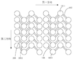
- FIG. 4 is a partial schematic diagram of the arrangement of first OLED pixels in a first display area of a display substrate according to an embodiment of the present application
- FIG. 5 is a schematic diagram of the arrangement of first pixel groups in the first display area shown in FIG. 4;
- FIG. 6 is a schematic diagram of the projection of the first electrode block on the substrate in the first display area shown in FIG. 4;
- FIG. 7 is a partial schematic diagram of the arrangement of first OLED pixels in the first display area of another display substrate provided by an embodiment of the present application;
- FIG. 8 is a schematic diagram of a projection of the first electrode block on the substrate in the first display area shown in FIG. 7;
- FIG. 9 is another schematic diagram of projection of the first electrode block on the substrate in the first display area shown in FIG. 7;
- FIG. 10 is a schematic diagram of still another projection of the first electrode block in the first display area shown in FIG. 7 on the substrate;
- FIG. 11 is a partial schematic diagram of the second OLED pixel arrangement in the second display area of the display substrate provided by the embodiment of the present application;
- FIG. 12 is another partial schematic diagram of the arrangement of the first OLED pixels in the first display area of the display substrate provided by the embodiment of this application;
- FIG. 13 is another partial schematic diagram of the second OLED pixel arrangement in the second display area of the display substrate provided by the embodiment of the present application;
- FIG. 14 is a partial cross-sectional view of a display substrate provided by an embodiment of the present application.
- 15 is a partial schematic diagram of the arrangement of pixel units in the first display area and the second display area of another display substrate provided by an embodiment of the present application;
- FIG. 16 is a partial schematic diagram of the arrangement of pixel units in the first display area and the second display area of still another display substrate provided by an embodiment of the present application.
- the photosensitive devices are arranged on the above electronic devices by setting a transparent display screen. Below the transparent display area, a full-screen display of the electronic device can be realized while ensuring the normal operation of the photosensitive device.
- the pixel density of the transparent display is generally set to be lower than the pixel density of the non-transparent display.
- the inventor found that when the electronic device is displayed, sometimes the image is deformed, which will affect the user experience.
- embodiments of the present application provide a display substrate, a display panel, and a display device, which can well solve the above-mentioned problems.
- the embodiment of the present application provides a display substrate. 1 and 2, the display area of the display substrate 100 includes a first display area 10 and a second display area 20.
- the light transmittance of the first display area 10 is greater than that of the second display area 20.
- the display substrate 100 may further include a substrate. 3, 4, and 7, a plurality of first pixel units 11 are provided in the first display area 10, and the first pixel units 11 include first organic light-emitting diodes (OLEDs) of n colors.
- OLEDs organic light-emitting diodes
- the pixels 111, 112, 113 for example, the first OLED pixels 111, 112, 113 respectively correspond to a different color. Referring to FIG.
- a plurality of second pixel units 21 are provided in the second display area 20, and the second pixel units 21 include second OLED pixels 211, 212, 213 of n colors, for example, second OLED pixels 211, 212, and 213 correspond to a different color.
- n is a natural number not less than 3.
- the first OLED pixel and the second OLED pixel are located on the substrate.
- the first OLED pixel 111 includes at least two first sub-pixels 101 arranged at intervals along the first direction.
- the first OLED pixel 112 includes at least two first sub-pixels 103 arranged at intervals along the first direction
- the first OLED pixel 113 includes at least two first sub-pixels arranged at intervals along the first direction.
- Sub-pixel 105 The first sub-pixels 101, 103, 105 that are adjacent and belong to different (for example, different corresponding colors) first OLED pixels are arranged at intervals in a second direction, and the first direction intersects the second direction.
- the first sub-pixels 101, 103, 105 include a first electrode block, a first light-emitting structure block arranged on the first electrode block, and a second electrode arranged on the first light-emitting structure block, the same ( For example, corresponding to the same color) the first electrode blocks of two adjacent first sub-pixels 101 in the first OLED pixel 111 are electrically connected. Similarly, the first electrode blocks of two adjacent first sub-pixels 103 in the same first OLED pixel 112 are electrically connected, and the first electrodes of two adjacent first sub-pixels 105 in the same first OLED pixel 113 are electrically connected. Block electrical connection.
- the ratio of the first size to the second size of the first pixel unit 11 and the ratio of the first size to the second size of the second pixel unit 21 are approximately the same.
- the first size is the size of the pixel unit in the first direction
- the second size is the size of the pixel unit in the second direction
- the first direction intersects the second direction. That is, the first size of the first pixel unit 11 is the size of the first pixel unit 11 in the first direction
- the second size of the first pixel unit 11 is the size of the first pixel unit 11 in the second direction
- the first size of the second pixel unit 21 is the size of the second pixel unit 21 in the first direction
- the second size of the second pixel unit 21 is the size of the second pixel unit 21 in the second direction.
- the light transmittance of the first display area 10 is greater than the light transmittance of the second display area 20, and the photosensitive device can be arranged under the first display area 10 to ensure normal operation of the photosensitive device Realize the full-screen display of the display substrate.
- the first OLED pixel includes at least two first sub-pixels, and in the same first OLED pixel, the first electrode blocks of two adjacent first sub-pixels are electrically connected, then the first sub-pixels of the same first OLED pixel One of the first electrode blocks only needs to be connected to the signal line or the pixel circuit, which can reduce the complexity of wiring and the structure of the first display area 10, thereby reducing the diffraction of external light when passing through the first display area 10.
- the influence of diffraction of external light on the photosensitive device disposed under the first display area 10 is reduced.
- the ratio of the first size to the second size of the first pixel unit 11 and the ratio of the first size to the second size of the second pixel unit 21 are approximately the same, then the shapes of the first pixel unit and the second pixel unit are compared
- the proximity can reduce the probability of image deformation of the display substrate 100 during display due to the large difference in shape between the first pixel unit and the second pixel unit, and improve the display effect of the display substrate 100, thereby enhancing the user experience.
- the ratio of the first size to the second size of the first pixel unit 11 is the first ratio
- the ratio of the first size to the second size of the second pixel unit 21 is the second ratio.
- the first ratio and the second ratio are approximately the same, including two situations: the first ratio and the second ratio are equal, or the difference between the first ratio and the second ratio is within a specified range.
- the first size of the first pixel unit 11 and the first size of the second pixel unit 21 may be the same or different.
- the area of the first pixel unit 11 is larger than the area of the second pixel unit 21, that is, the first size of the first pixel unit 11 is larger than the first size of the second pixel unit 21, and the second size of the first pixel unit It is larger than the second size of the second pixel unit 21.
- At least two first sub-pixels of the same first OLED pixel are arranged at intervals along the first direction, which means that at least two first sub-pixels of the same first OLED pixel are generally arranged along the first direction.
- the direction is arranged.
- the axes along the first direction of at least two first sub-pixels of the same first OLED pixel may or may not overlap.
- FIGS. 4 and 7 multiple first sub-pixels of the same first OLED pixel The sub-pixels are misaligned in the first direction, and it is also considered that the multiple first sub-pixels of the same first OLED pixel are arranged at intervals along the first direction.
- the adjacent first sub-pixels belonging to different first OLED pixels are arranged at intervals in the second direction, which may include two situations:
- the n first OLED pixels included in the same first pixel unit 11 are arranged at intervals along the second direction, and the first sub-pixels included in the same first OLED pixel are all located in another one.
- the same side of the first OLED pixel for example, an adjacent first OLED pixel.
- the first sub-pixels are arranged at intervals in the second direction.
- the first sub-pixels 103 included in the first OLED pixel 112 in FIG. 7 are all located on the same side of the first OLED pixel 113.
- the first sub-pixels belonging to two adjacent first OLED pixels are arranged at intervals in the second direction. For example, part of the first sub-pixel 103 of the first OLED pixel 112 in FIG.
- first sub-pixel 103 and first sub-pixels 105 are arranged at intervals in the second direction.
- the size of the first pixel unit 11 in the first direction refers to the maximum size of the first pixel unit 11 in the first direction
- the size of the first pixel unit 11 in the second direction refers to the size of the first pixel unit 11 in the first direction.
- the largest dimension in the second direction refers to the maximum dimension of the second pixel unit 21 in the first direction
- the size of the second pixel unit 21 in the second direction refers to the size of the second pixel unit 21 in the first direction.
- first direction and the second direction may be perpendicular to each other.
- the first direction may be a row direction and the second direction may be a column direction; or, the first direction may be a column direction, and the second direction may be a row direction.
- FIGS. 4 to 10 only use the first direction as the row direction and the second direction as the column direction as examples for illustration, and other cases will not be illustrated.
- the arrangement law of the first sub-pixels in the first pixel unit 11 is consistent with the arrangement law of the second OLED pixels in the second pixel unit.
- the arrangement law of pixels refers to the arrangement of pixels, for example, it can be the arrangement order and arrangement position relationship of adjacent pixels of the same color, arrangement order and arrangement position of pixels of different colors, etc.
- the arrangement of pixels is not necessarily related to the size of the pixel unit where the pixels are located.
- the arrangement of the first sub-pixels in the first pixel unit 11 and the arrangement of the second OLED pixels in the second pixel unit 21 are the same, but the first size of the first pixel unit 11 is the same as that of the second pixel unit.
- the first size of 21, the second size of the first pixel unit 11, and the second size of the second pixel unit 21 may be different.
- the first display area 10 and the second display of the display substrate 100 can be The display effect of the area 20 is more consistent, which is beneficial to improve the user experience.
- n 3, that is, the first pixel unit 11 includes first OLED pixels of three different colors, and the second pixel unit 21 includes second OLED pixels of three different colors.
- the three colors can be red, green and blue, or other colors.
- the three colors are red, green, and blue as examples, and the three colors are other colors.
- the value of n may also be greater than 3.
- the first pixel unit 11 includes a red first OLED pixel 111, a green first OLED pixel 112, and a blue first OLED pixel 113
- the red first OLED pixel 111 includes At least two red first sub-pixels 101
- the green first OLED pixel 112 includes at least two green first sub-pixels 103
- the blue first OLED pixel 113 includes at least two blue first sub-pixels One sub-pixel 105.
- the second pixel unit 21 may include a red second OLED pixel 211, a green second OLED pixel 212, and a blue second OLED pixel 213. Further, the number of the red second OLED pixel 211, the green second OLED pixel 212 and the blue second OLED pixel 213 in the second pixel unit 21 is one respectively.
- the first sub-pixels of different colors in the first pixel unit 11 may be arranged in a magenta shape, that is, arranged in a triangle; the second OLEDs of different colors in the second pixel unit 21 are adjacent to each other.
- the pixels can be arranged in a fringe shape, that is, in a triangular arrangement.
- the red first sub-pixel 101, the green first sub-pixel 103, and the blue first sub-pixel 105 are arranged in a magenta shape.
- the red second OLED pixel 211, the green second OLED pixel 212, and the blue second OLED pixel 213 are arranged in a magenta shape.
- the adjacent second OLED pixels corresponding to the three colors in the second pixel unit 21 and the adjacent first sub-pixels corresponding to the three colors in the first pixel unit 11 are all arranged in a triangle or magenta shape, so that When the display substrate 100 is displayed, the display effects of the first display area 10 and the second display area 20 are more consistent, which is beneficial to improving the user experience.
- the distribution of the first sub-pixels of the same color is relatively uniform, so that the openings on the mask plate of the first light-emitting structure block of the first sub-pixels are arranged regularly, which can reduce the wrinkles of the mask plate;
- the distribution of the second OLED pixels is relatively uniform, so that the arrangement of the openings on the mask plate for preparing the second OLED pixels is relatively regular, which can reduce the wrinkles of the mask plate.
- the first pixel unit 11 includes three first OLED pixels, and each first OLED pixel includes four first sub-pixels arranged at intervals along the first direction. Since the first pixel unit 11 includes three first OLED pixels of different colors, and the number of first OLED pixels included in the first pixel unit 11 is three, the first OLED pixels of each color in the first pixel unit 11 The number is only one, that is, the first pixel unit 11 includes a red first OLED pixel 111, a green first OLED pixel 112, and a blue first OLED pixel 113.
- the red first OLED pixel 111 includes four red first sub-pixels 101 arranged at intervals along the first direction
- the green first OLED pixel 112 includes four green first sub-pixels arranged at intervals along the first direction.
- the sub-pixels 103 and the blue first OLED pixel 113 include four blue first sub-pixels 105 arranged at intervals along the first direction.
- the overall shape of the first pixel unit 11 is roughly rectangular, and the shape is relatively regular.
- the pattern displayed in the first display area 10 is not easily deformed, and the quality of the image displayed in the first display area 10 can be improved.
- the shape of the first pixel unit 11 can be made closer to the shape of the second pixel unit 21, so that the display effects of the first display area 10 and the second display area 20 are more consistent.
- the first pixel unit 11 is provided to include three first OLED pixels, and each first OLED pixel includes four first sub-pixels arranged at intervals along the first direction, which can ensure that the overall shape of the first pixel unit 11 is approximately Under the premise of being rectangular, the density of the first pixel units 11 in the first display area 10 is made higher, which helps to improve the display effect of the first display area 10.
- the first pixel unit 11 may also include six first OLED pixels, and each first OLED pixel includes six first sub-pixels arranged at intervals along the first direction. That is, the first pixel unit 11 includes two red first OLED pixels 111, two green first OLED pixels 112, and two blue first OLED pixels 113. Wherein, each red first OLED pixel 111 includes six red first sub-pixels 101 arranged at intervals along the first direction, and each green first OLED pixel 112 includes six arranged at intervals along the first direction. The green first sub-pixels 103, and each blue first OLED pixel 113 includes six blue first sub-pixels 105 arranged at intervals along the first direction. With this arrangement, the overall shape of the first pixel unit 11 can also be roughly rectangular, with a relatively regular shape.
- the first sub-pixels in the first pixel unit 11 can be divided into at least two first pixel groups 110 arranged along the second direction, and each first pixel group 110 can be arranged along the Extend in the first direction.
- the first sub-pixels in one first pixel group 110 can be arranged in a first order
- the first sub-pixels in the other first pixel group 110 can be arranged in a second order arrangement.
- the first order may be a red first sub-pixel 101, a green first sub-pixel 103, and a blue first sub-pixel 105
- the second order may be a blue first sub-pixel 105
- the first sub-pixel 103 is green and the first sub-pixel 101 is red.
- the magenta shape formed by the first sub-pixels arranged in the first order may be the shape formed by the mignon inclined 90 degrees to the right according to the orientation shown in FIG. 5, and the magenta shape formed by the first sub-pixels arranged in the second order may be It is the shape of the product character inclined 90 degrees to the left according to the orientation shown in Figure 5.
- the first sub-pixels in the first pixel unit 11 shown in FIG. 5 are divided into two first pixel groups 110.
- the first sub-pixels in one of the first pixel groups 110 are arranged in a first order, and the other The first sub-pixels in the pixel group 110 are arranged in a second order.
- the first sub-pixels in the first pixel unit 11 can also be divided into three or more first pixel groups 110. With this arrangement, the colors of the first sub-pixels adjacently arranged in the first direction in the first display area 10 are all different, and the first sub-pixels of the same color are more evenly distributed in the first display area 10, which is beneficial to The display effect of the first display area 10 is improved.
- the first sub-pixels of two adjacent first pixel groups 110 of the first pixel unit 11 are arranged at intervals in the second direction, and the The colors of the three first sub-pixels spaced apart in the direction are different.
- the three first sub-pixels arranged at intervals in the second direction are respectively a red first pixel 101 and a green first sub-pixel.
- the pixel 103 and the blue first sub-pixel 105 are all different, and the distribution of the first sub-pixels of the same color is more uniform, which can avoid some problems in the first display area 10.
- first sub-pixels of the same color in a region are adjacent to each other, resulting in uneven color distribution during the display of the first display area 10, which in turn leads to the problem of single-color bright bars in the region, which can improve the performance of the first display area 10. display effect.
- the second display area 20 may include a plurality of second pixel groups 210 arranged along the second direction, and each second pixel group 210 may be along the first direction. extend.
- each second pixel group 210 may include a second pixel unit 21.
- the second OLED pixels in one second pixel group 210 are arranged in the third order
- the second OLED pixels in the other second pixel group 210 are arranged in the fourth order
- the third sequence is a red second OLED pixel 211, a green second OLED pixel 212, and a blue second OLED pixel 213, and the fourth sequence is a blue second OLED pixel 213, and a green second OLED pixel.
- the OLED pixel 212, the red second OLED pixel 211 may be a shape formed by the magenta character inclined 90 degrees to the right according to the orientation shown in FIG. 11, and the magenta shape formed by the second OLED pixels arranged in the fourth order It can be a shape in which the character is inclined 90 degrees to the left according to the orientation shown in FIG. 11.
- the colors of the second OLED pixels adjacently arranged in the first direction in the second display area 20 are all different, and the second OLED pixels of the same color are more evenly distributed in the second display area 20, which is beneficial to Improve the display effect of the second display area 20.
- three second OLED pixels are arranged at intervals in the second direction, and as shown in FIG. 11, adjacent In the two second pixel groups 210, the three second OLED pixels arranged at intervals in the second direction are respectively a red second OLED pixel 211, a green second OLED pixel 212, and a blue second OLED pixel. Pixel 213.
- the colors of the second OLED pixels adjacently arranged in the second direction in the second display area 20 are all different, so that the second OLED pixels of the same color are more evenly distributed, which can avoid the second display area 20
- multiple second OLED pixels of the same color are adjacent to each other, resulting in uneven color distribution during display of the second display area 20, which in turn leads to the problem of a single color bright bar in the area, which can increase the second display area 20.
- the display effect is
- a plurality of first OLED pixels in the same first pixel unit 11 may be arranged in parallel in the second direction, and the second OLED pixels in the second pixel unit 21 may be arranged in parallel in the second direction.
- Arrangement. 12 in the first pixel unit 11, the red first OLED pixel 111, the green first OLED pixel 112, and the blue first OLED pixel 113 are spaced apart and arranged side by side in the second direction, so that the first pixel In the unit 11, the red first sub-pixel 101, the green first sub-pixel 103, and the blue first sub-pixel 105 are spaced apart and arranged side by side in the second direction, for example, aligned in the second direction. Referring to FIG.
- the red second OLED pixel 211, the green second OLED pixel 212, and the blue second OLED pixel 213 are spaced apart and arranged side by side in the second direction.
- the arrangement rule of the first sub-pixels in the first pixel unit is consistent with the arrangement rule of the second OLED pixels in the second pixel unit.
- the colors of three adjacent first sub-pixels are different;
- the second OLED pixels arranged in the second direction three adjacent second OLED pixels have different colors.
- three adjacent first sub-pixels are respectively a red first sub-pixel 101 and a green second sub-pixel.
- three adjacent second OLED pixels are respectively a red second OLED pixel 211 and a green second OLED pixel.
- This configuration can make the arrangement of the first sub-pixels in the first pixel unit and the second OLED pixels in the second pixel unit more similar, which helps to improve the display of the first display area 10 and the second display area 20 Consistency of effect.
- the first pixel unit 11 may further include a connecting bar, which connects the first electrode blocks of the first OLED pixels of the same color.
- the same first OLED pixel includes a connecting portion connecting the first electrode blocks of two adjacent first sub-pixels.
- the connecting bar of the first OLED pixel may be arranged on the same layer as the first electrode block of the first OLED pixel, or may be arranged on a different layer from the first electrode block of the first OLED pixel. Regardless of which layer the connecting strips are arranged on, it is necessary to ensure that the connecting strips arranged on the same layer do not intersect the connecting parts.
- the arrangement of the first sub-pixels of the first OLED pixel in the first pixel unit may be different from that of FIG. 4, FIG. 7 or FIG. 12.
- the arrangement of the second OLED pixels in the second pixel unit is The arrangement method can also be different from the arrangement patterns of FIGS. 11 and 13, as long as the arrangement law of the first sub-pixels in the first pixel unit is consistent with the arrangement law of the second OLED pixels in the second pixel unit.
- two adjacent first sub-pixels may be arranged in a staggered manner in the second direction . That is, in the first electrode block of the first OLED pixel, the two adjacent first electrode blocks are arranged in a staggered manner in the second direction. This arrangement can further reduce the incidence of external light passing through the first display area of the display substrate 100 Diffraction effect at 10 o'clock.
- two first sub-pixels arranged at intervals of one first sub-pixel are arranged in the first side.
- the upward central axis may coincide.
- the arrangement of the first light-emitting structure blocks of the same first OLED pixel is more regular, and the opening arrangement of the mask used to prepare the light-emitting structure block is more regular.
- the same mask can be used to fabricate in the same evaporation process. Since the pattern on the mask is more uniform, it also reduces The net folds.
- the same first pixel unit may further include a plurality of connecting portions.
- the first OLED pixel 111 may include at least one connecting portion 102
- the first OLED pixel 112 may include at least one connecting portion.
- Part 104, the first OLED pixel 113 may include at least one connection part 106.
- two adjacent first electrode blocks 1011 are electrically connected through corresponding connecting portions. Among them, the adjacent first electrode blocks in the red first OLED pixel 111 are electrically connected through the connection part 102, the adjacent first electrode blocks in the green first OLED pixel 112 are electrically connected through the connection part 104, and the blue first electrode block is electrically connected through the connection part 104. Adjacent first electrode blocks in an OLED pixel 113 are electrically connected through the connecting portion 106.
- the display substrate 100 further includes a substrate, and the first OLED pixel and the second OLED pixel are located on the substrate.
- the projections of the connecting portions of different first OLED pixels on the substrate may intersect.
- the projections of the connecting portion 102 and the connecting portion 104 on the substrate intersect the projections of the connecting portion 106 on the substrate, respectively.
- the number of the connecting portions 102, 104, 106 in the same first pixel unit is multiple, at least part of the connecting portions and the corresponding first electrode block 1011 are respectively arranged on different layers.
- the wiring method of the connecting parts is more flexible.
- the size of the first electrode block 1011 is not affected by the connection portion provided in a different layer from the first electrode block 1011.
- the connecting portions of the different first OLED pixels are on the substrate.
- the projections do not intersect.
- the projections of the connecting portion 102, the connecting portion 104, and the connecting portion 106 on the substrate in FIG. 7 do not intersect.
- the connecting parts of each first OLED pixel can be arranged on the same layer or on different layers.
- the connecting portion and the corresponding first electrode block 1011 may be provided on the same layer, or may be provided on a different layer.
- the connecting portions of the first pixel unit 11 and the corresponding first electrode block 1011 can be respectively arranged on the same layer, and the first electrode block 1011 and the connecting portions 102, 104, 106 of the first pixel unit 11 can be in the same process. It is formed in the steps, which can reduce the complexity of the preparation process to a certain extent.
- the connecting portion and the corresponding first electrode block 1011 are arranged on different layers, the connecting portion may be respectively arranged under the corresponding first electrode block 1011. With this arrangement, the connecting portion will not affect the display of the first OLED pixel.
- the display substrate 100 further includes a pixel circuit for driving the first OLED pixel.
- the pixel circuit corresponding to the first OLED pixel may be a 1T circuit, or a 2T1C circuit, or a 3T1C circuit, or a 3T2C circuit, or a 7T1C circuit, or a 7T2C circuit.
- T stands for transistor and C stands for capacitance.
- the connecting portion of the same first OLED pixel and the corresponding first electrode block 1011 are located on different layers, the connecting portion of the first OLED pixel can be arranged on the same layer as the gate electrode of the transistor, or on the same layer as the upper plate of the capacitor , Or arranged on the same layer as the source electrode of the transistor.
- the display substrate 100 further includes a substrate, the first OLED pixel and the second OLED pixel are located on the substrate, and the number of connecting portions in the same first pixel unit 11 is greater.
- the connecting parts whose projections intersect on the substrate may be arranged on different layers, and the connecting parts whose projections on the substrate do not intersect may be arranged on the same layer or different layers.
- This arrangement can prevent the normal operation of the first OLED pixel from affecting the normal operation of the first OLED pixel when the connecting parts where the projections on the substrate intersect are arranged on the same layer.
- these connecting portions can be formed in the same process step, thereby reducing the complexity of the manufacturing process.
- the connecting parts of the first OLED pixel may be arranged on the same layer.
- multiple connecting portions of the same first OLED pixel can be formed in the same process step, which can simplify the complexity of the work.
- the multiple connecting portions 102 included in the red first OLED pixel 111 are arranged on the same layer
- the multiple connecting portions 104 included in the green first OLED pixel 112 are arranged on the same layer
- the blue first OLED pixel 113 includes A plurality of connection parts 106 are provided on the same layer.
- the red first OLED pixel 111 includes the connecting portion 102 and the green
- the projections of the connecting portion 104 included in the first OLED pixel 112 on the substrate do not intersect, and can be arranged on the same layer.
- the projections of the connecting portion 106 included in the blue first OLED pixel 113 with the connecting portion 102 included in the red first OLED pixel 111 and the connecting portion 104 included in the green first OLED pixel 112 on the substrate are both If they intersect, the connecting portion 106 included in the blue first OLED pixel 113, the connecting portion 102 included in the red first OLED pixel 111 and the connecting portion 104 included in the green first OLED pixel 112 are arranged in different layers.
- the connecting portion 102 included in the red first OLED pixel 111 and the connecting portion 104 included in the green first OLED pixel 112 can be respectively arranged on the same layer as the corresponding first electrode block 1011, and the blue first OLED pixel 113
- the included connecting portion 106 and the corresponding first electrode block 1011 are arranged on different layers.
- the connecting portion 102 included in the red first OLED pixel 111 and the connecting portion 104 included in the green first OLED pixel 112 and the corresponding first electrode block 1011 are respectively arranged on different layers.
- the connecting portion 106 included in the blue first OLED pixel 113 and the corresponding first electrode block 1011 are arranged on the same layer; or, the connecting portion 106 included in the blue first OLED pixel 113 is connected to the red first OLED pixel 111
- the included connecting portion 102 and the connecting portion 104 included in the first green OLED pixel 112 are arranged in different layers, and the connecting portions included in the first OLED pixel of the three colors are all arranged in different layers from the corresponding first electrode block 1011.
- the size of the connecting portion perpendicular to its extension direction is greater than 3 ⁇ m and smaller than the first One half of the maximum size of the electrode block 1011.
- the size of the connecting portion perpendicular to its extending direction is a size on a plane extending in the first direction and the second direction.
- the resistance of the connecting portion can be made smaller; by setting the size of the connecting portion to be less than half of the maximum size of the first electrode block 1011, the size of the connecting portion can be made.
- the setting has a small influence on the size of the first electrode block 1011, and avoids that the size of the connecting portion is large, which causes the size of the first electrode block 1011 to decrease, which in turn causes the effective light-emitting area of the first display area 10 to decrease.
- the first pixel unit 11 when the first pixel unit 11 includes two or more first OLED pixels with the same color, among the two or more first OLED pixels with the same color, first electrode blocks of different first OLED pixels Electrically connected, or the first electrode block of one first OLED pixel is electrically connected to the first electrode block of another first OLED pixel. Further, the first pixel unit may also be provided with a connecting bar. Among the first OLED pixels of the same color, the first electrode blocks of different first OLED pixels may be electrically connected through the connecting bar, or the first OLED pixel The electrode block may be electrically connected to the first electrode block of another first OLED pixel through a connection bar.
- the first pixel unit 11 includes two red first OLED pixels 111, two green first OLED pixels 112 and two blue first OLED pixels 113.
- the first electrode blocks of the two red first OLED pixels 111 are electrically connected through the connecting bar 107
- the first electrode blocks of the two green first OLED pixels 112 are electrically connected through the connecting bar 108
- the two blue first electrode blocks are electrically connected
- the first electrode block of an OLED pixel 113 is electrically connected through the connection part 109.
- the connecting bar electrically connects the first electrode blocks of the two first OLED pixels with the same color, which can be achieved in the following two ways: one connecting portion of one first OLED pixel and one connecting portion of the other first OLED pixel pass through The connecting bars are connected together; or, a first electrode block of one of the first OLED pixels and a first electrode block of another first OLED pixel are connected together by the connecting bars.
- the projection of the first electrode block 1011 on the substrate may include one first pattern unit or a plurality of connected first pattern units.
- the first graphic unit includes a circle, an oval, a dumbbell, a gourd or a rectangle.
- the dumbbell shape refers to the shape of a pattern formed by connecting two circles with two parallel straight lines between the two circles with a distance smaller than the diameter of the two circles
- the gourd shape refers to the direct connection of two circles The shape of the pattern formed.
- the first graphic unit shown in FIGS. 6 and 8 is rectangular
- the first graphic unit shown in FIG. 9 is circular
- the first graphic unit shown in FIG. 10 is dumbbell-shaped.
- the above-mentioned shape can change the periodic structure produced by diffraction, that is, change the distribution of the diffraction field, thereby reducing the external incident light passing through the first display area 10.
- the diffraction effect generated at the time thereby ensuring that the image captured by the camera provided below the first display area 10 has a higher definition.
- the projection of the first light-emitting structure block in the first display area 10 on the substrate may include a second graphic unit or a plurality of connected second graphic units, and the second graphic unit is connected to the The first graphic units may be the same or different.
- the projection of the first light-emitting structure block corresponding to the first electrode block 1011 on the substrate is different from the projection of the first electrode block 1011 on the substrate, so as to further reduce light passing through the first Diffraction effect when displaying area 10.
- the second graphic unit may include a circle, an oval, a dumbbell, a gourd or a rectangle.
- the above-mentioned shape can change the periodic structure produced by diffraction, that is, change the distribution of the diffraction field, thereby further reducing the external incident light passing through the first display area
- the diffraction effect that occurs at 10 o'clock further ensures that the image taken by the camera located below the first display area 10 has a higher definition.
- the first electrode block 1011 may be an anode
- the second electrode may be a cathode
- the second electrode may be a surface electrode
- the light transmittance of the first electrode block 1011 and/or the second electrode may be greater than or equal to 70%. Further, the light transmittance of the first electrode block 1011 and/or the second electrode may be greater than or equal to 90%, for example, the light transmittance may be 90%, 95%, etc. Such an arrangement can make the light transmittance of the first display area 10 larger, so that the light transmittance of the first display area 10 meets the lighting requirements of the photosensitive device disposed below it.
- the material of the first electrode block 1011 may include indium tin oxide, indium zinc oxide, indium tin zinc oxide, silver-doped indium tin oxide, silver-doped indium zinc oxide or graphene. At least one.
- the material of the first electrode block 1011 is silver-doped indium tin oxide or silver-doped indium zinc oxide, so as to ensure the high light transmittance of the first display area 10 and reduce the first electrode Block 1011 resistance.
- the material of the second electrode may include at least one of indium tin oxide, indium zinc oxide, silver-doped indium tin oxide, silver-doped indium zinc oxide, graphene, magnesium, silver, or aluminum.
- the material of the second electrode is silver-doped indium tin oxide or silver-doped indium zinc oxide to reduce the resistance of the second electrode on the basis of ensuring high light transmittance of the first display area 10 .
- the driving mode of the first OLED pixel may be passive driving or active driving.
- the driving mode of the first OLED pixel is an active driving mode, each of the first OLED pixels is driven by a pixel circuit.
- the first display area 10 may be adjacent to the second display area 20, the first display area 10 may be at least partially surrounded by the second display area 20, and the When the driving mode of the first OLED pixel is active driving, the pixel circuit corresponding to the first OLED pixel may be arranged in the second display area 20.
- This configuration can reduce the complexity of the structure under the first OLED pixel in the first display area 10, and can reduce the complexity of the wiring under the first OLED pixel in the first display area 10, which helps to improve light transmission.
- the resulting diffraction superposition phenomenon further improves the quality of the image taken by the camera arranged under the first display area 10.
- the pixel circuit corresponding to the first OLED pixel may be arranged in an area of the second display area 20 adjacent to the first display area 10. With this arrangement, the length of the wiring between the first electrode block for the first OLED pixel and the corresponding pixel circuit can be shortened.
- the display area of the display substrate 100 may further include a transition display area 30 located between the first display area 10 and the second display area 20.
- the driving mode of the OLED pixel is active driving
- the pixel circuit corresponding to the first OLED pixel may be arranged in the transition display area 30.
- This arrangement can also reduce the complexity of the structure under the first OLED pixel in the first display area 10, and can reduce the complexity of the wiring under the first OLED pixel in the first display area 10, and help improve light transmission. The phenomenon of diffraction and superposition generated during the time, thereby further improving the quality of the image taken by the camera disposed under the first display area 10.
- the pixel circuit corresponding to the first OLED pixel may be arranged in an area of the transition display area 30 close to the first display area 10. With this arrangement, the length of the wiring between the first electrode block for the first OLED pixel and the corresponding pixel circuit can be shortened.
- a plurality of third pixel units are provided in the transition display area 30, and the density of the third pixel units may be equal to the density of the first pixel units in the first display area 10.
- the density of the third pixel unit may be equal to the density of the second pixel unit.
- the density of the third pixel unit may also be different from the density of the first pixel unit and the density of the second pixel unit. For example, it may be greater than the density of the first pixel unit and smaller than the density of the first pixel unit. The density of the two-pixel unit.
- the third pixel unit may include third OLED pixels of n colors, and n is a natural number not less than 3.
- Each of the third OLED pixels may include at least two third sub-pixels arranged at intervals along the first direction, and the third sub-pixels may include a third electrode block, and a second electrode block disposed on the third electrode block.
- the two light-emitting structure blocks and the fourth electrode arranged on the second light-emitting structure block are electrically connected to adjacent third electrode blocks in the same third OLED pixel.
- the first size of the third pixel unit may be larger than the first size of the second pixel unit and smaller than the first size of the first pixel unit.
- the first size of the pixel unit in the first direction gradually transitions from the first display area to the second display area, which helps to improve the display effect.
- the first electrode block of the first OLED pixel may be electrically connected to the corresponding pixel circuit through a transparent wiring. Since at least part of the transparent wiring is located in the first display area 10, this arrangement can further improve the light transmittance of the first display area 10.
- the light transmittance of the transparent wiring is greater than or equal to 50%. More preferably, the light transmittance of the transparent wiring may be greater than 70%, for example, 80%, 90%, etc., to further improve the light transmittance of the first display area 10.
- the material of the transparent wiring may include at least one of indium tin oxide, indium zinc oxide, silver-doped indium tin oxide, silver-doped indium zinc oxide, or graphene.
- the material of the transparent wiring is silver-doped indium tin oxide or silver-doped indium zinc oxide to reduce the resistance of the transparent wiring on the basis of ensuring high light transmittance of the transparent wiring.
- a first pixel defining layer 120 may be further provided in the first display area 10, and the first pixel defining layer 120 is provided on the first electrode block 1011, and The first pixel defining layer 120 is provided with a plurality of first pixel openings, and the plurality of first light-emitting structure blocks 114 are arranged in the plurality of first pixel openings in a one-to-one correspondence.
- the second OLED pixel includes a fifth electrode block 2011, a third light-emitting structure block 214 disposed on the fifth electrode block 2011, and a sixth electrode (not shown) disposed on the third light-emitting structure block 214 ), the second display area 20 may further be provided with a second pixel defining layer 220, the second pixel defining layer 220 is disposed on the fifth electrode block 2011, and the second pixel defining layer 220 is provided with There are a plurality of second pixel openings, and a plurality of the third light-emitting structure blocks 214 are arranged in the plurality of second pixel openings in a one-to-one correspondence.
- the light transmittance of the first pixel defining layer 120 is greater than the light transmittance of the second pixel defining layer 220. With this arrangement, the light transmittance of the first display area 10 can be increased, and thus the imaging effect of the camera arranged under the first display area 10 can be improved.
- the light transmittance of the first pixel defining layer 120 is greater than 70%. Furthermore, the light transmittance of the first pixel defining layer 120 is greater than 90%, for example, it may be 90%, 92%, 95%, etc., so that the light transmittance effect of the first display area 10 is better.
- the material of the first pixel defining layer 120 may include polyorganosiloxane. This can ensure that the light transmittance of the first pixel defining layer 120 is high.
- the material of the second pixel defining layer 220 may include at least one of polyvinylpyridine or photosensitive polyimide. In this way, the properties of the second pixel defining layer 220 are relatively stable and the service life is longer.
- the display area of the display substrate 100 includes a first display area 10 and a second display area 20.
- the light transmittance of the first display area 10 is The light transmittance of the second display area 20 is greater than that.
- a plurality of first pixel units 11 are provided in the first display area 10
- the first pixel units 11 include first OLED pixels 111, 112, 113 of n colors
- a plurality of second pixel units 21 are provided in the second display area 20.
- the second pixel units 21 include second OLED pixels 211, 212, and 213 of n colors, and n is a natural number not less than 3.
- the density of the first pixel unit 11 is less than the density of the second pixel unit 21.
- the ratio of the first size to the second size of the first pixel unit 11 and the ratio of the first size to the second size of the second pixel unit 21 are approximately the same.
- the first size is the size of the pixel unit in the first direction
- the second size is the size of the pixel unit in the second direction
- the first direction intersects the second direction. That is, the first size of the first pixel unit 11 is the size of the first pixel unit 11 in the first direction
- the second size of the first pixel unit 11 is the size of the first pixel unit 11 in the second direction
- the first size of the second pixel unit 21 is the size of the second pixel unit 21 in the first direction
- the second size of the second pixel unit 21 is the size of the second pixel unit 21 in the second direction.
- the light transmittance of the first display area 10 is greater than the light transmittance of the second display area 20, and the photosensitive device can be arranged under the first display area 10 to ensure normal operation of the photosensitive device Realize the full-screen display of the display substrate.
- the ratio of the first size to the second size of the first pixel unit 11 and the ratio of the first size to the second size of the second pixel unit 21 are approximately the same, then the shapes of the first pixel unit and the second pixel unit are compared
- the proximity can reduce the probability of image deformation of the display substrate 100 during display due to the large difference in shape between the first pixel unit and the second pixel unit, and improve the display effect of the display substrate 100, thereby enhancing the user experience.
- n 3, that is, the first pixel unit 11 includes first OLED pixels of three different colors, and the second pixel unit 21 includes second OLED pixels of three different colors.
- the three colors can be red, green and blue, or other colors.
- the three colors are red, green, and blue as examples, and the three colors are other colors.
- the value of n may also be greater than 3.
- the arrangement law of the first OLED pixels in the first pixel unit 11 is consistent with the arrangement law of the second OLED pixels in the second pixel unit 21.
- the arrangement of the first OLED pixels in the first pixel unit is consistent with the arrangement law of the second OLED pixels in the second pixel unit 21.
- the adjacent first OLED pixels of different colors in the first pixel unit 11 may be arranged in a magenta shape, and the adjacent second OLED pixels of different colors in the second pixel unit 21 may be in a magenta shape. arrangement. Referring to FIG. 15, in the first pixel unit 11, the red first OLED pixel 111, the green first OLED pixel 112, and the blue first OLED pixel 113 are arranged in a magenta shape; the red second OLED pixel in the second pixel unit The pixels 211, the green second OLED pixel 212, and the blue second OLED pixel 213 are arranged in a magenta shape.
- the specific arrangement order and positional relationship of the first OLED pixels in the first pixel unit 11 are similar to the arrangement order and positional relationship of the first sub-pixels in FIG. 4, and the specific arrangement of the second OLED pixels in the second pixel unit 21
- the arrangement order and positional relationship are similar to the specific arrangement order and positional relationship of the second OLED pixels in FIG. 11.
- the multiple first OLED pixels in the same first pixel unit 11 are arranged side by side in the second direction; the second OLED pixels in the second pixel unit 21 are Arrange side by side in the second direction.
- the specific arrangement order and positional relationship of the first OLED pixels in the first pixel unit 11 are similar to the arrangement order and positional relationship of the first sub-pixels in FIG. 12, and the specific arrangement of the second OLED pixels in the second pixel unit 21
- the arrangement order and positional relationship are similar to the specific arrangement order and positional relationship of the second OLED pixels in FIG. 13.
- the driving mode of the first OLED pixel may be active driving
- the first display area 10 may be provided with a pixel circuit corresponding to the first OLED pixel one to one, and the first display area Among the pixel circuits of each first OLED pixel, at least part of the pixel circuits of the first OLED pixel are arranged in the first display area.
- the pixel circuit of the first OLED pixel is a 1T circuit, or a 2T1C circuit, or a 3T1C circuit, or a 3T2C circuit, or a 7T1C circuit, or a 7T2C circuit.
- T represents a transistor
- C represents a capacitor, that is, the pixel circuit of the first OLED pixel includes a transistor and/or a capacitor.
- the transistors and/or capacitors of the pixel circuit arranged in the first display area 10 may be made of a transparent conductive material. In this way, the light transmittance of the first display area 10 can be improved.
- the light transmittance of the transparent conductive material is greater than 70%. Furthermore, the light transmittance of the transparent conductive material may be greater than or equal to 90%, for example, the light transmittance may be 90%, 95%, etc. Such an arrangement can make the light transmittance of the first display area 10 larger, so that the light transmittance of the first display area 10 meets the lighting requirements of the photosensitive device disposed below it.
- the transparent conductive material may include at least one of indium tin oxide, indium zinc oxide, silver-doped indium tin oxide, silver-doped indium zinc oxide, or graphene.
- the transparent conductive material is silver-doped indium tin oxide or silver-doped indium zinc oxide, so as to reduce the resistance of transistors and/or capacitors on the basis of ensuring high light transmittance of the first display area 10 .
- the transistors and/or capacitors of the pixel circuit arranged in the first display area 10 are made of opaque conductive materials.
- the opaque conductive material can be metallic molybdenum, metallic copper, metallic aluminum, etc., which can make the resistance of transistors and capacitors small.
- the opaque conductive material may be covered with a light-shielding material.
- the light-shielding material arranged on the transistor and the capacitor can prevent the external incident light from shining on the transistor and the capacitor, and affect the properties of the transistor and the capacitor.
- the light-shielding material may include at least one of silver oxide or vinyl.
- the first OLED pixel may include a first electrode block, a light emitting structure block disposed on the first electrode block, and a second electrode disposed on the light emitting structure block.
- the second OLED pixel may include a fifth electrode block, a third light-emitting structure block provided on the fifth electrode block, and a sixth electrode provided on the third light-emitting structure block.
- the first display area 10 may also be provided with a first pixel defining layer, the first pixel defining layer is disposed on the first electrode block, and a plurality of first pixels are opened on the first pixel defining layer Openings, a plurality of first light-emitting structure blocks are arranged in the plurality of first pixel openings in a one-to-one correspondence.
- a second pixel defining layer may be further provided in the second display area 20, the second pixel defining layer is disposed on the fifth electrode block, and a plurality of second pixels are opened on the second pixel defining layer Openings, a plurality of the third light-emitting structure blocks are arranged in the plurality of second pixel openings in one-to-one correspondence.
- the light transmittance of the first pixel defining layer is greater than the light transmittance of the second pixel defining layer.
- the light transmittance of the first pixel defining layer is greater than 70%. Furthermore, the light transmittance of the first pixel defining layer is greater than 90%, for example, it can be 90%, 92%, 95%, etc., so that the light transmittance effect of the first display area 10 is better.
- the material of the first pixel defining layer may include polyorganosiloxane. This can ensure that the light transmittance of the first pixel defining layer is high.
- the material of the second pixel defining layer may include at least one of polyvinylpyridine and photosensitive polyimide. In this way, the properties of the second pixel defining layer are relatively stable and the service life is longer.
- first direction and the second direction may be perpendicular to each other.
- the first direction may be a row direction and the second direction may be a column direction; or, the first direction may be a column direction, and the second direction may be a row direction.
- FIGS. 15 to 16 only take the first direction as the row direction and the second direction as the column direction as examples for illustration, and other cases are not illustrated again.
- An embodiment of the present application also provides a display panel, which includes any of the above-mentioned display substrate 100 and a packaging structure.
- the packaging structure is disposed on the side of the display substrate 100 away from the substrate.
- the packaging structure may include a polarizer, and the polarizer covers at least the second display area 20. Further, the polarizer does not cover the first display area 10, and a photosensitive device that emits or collects light passing through the first display area 10 may be disposed under the first display area 10.
- the polarizer can dissipate the reflected light on the surface of the display panel and improve the user experience; the first display area 10 is not provided with a polarizer, which can increase the light transmittance of the first display area 10 and ensure that the photosensitive device is arranged under the first display area 10 Works normally.
- An embodiment of the present application also provides a display device, which includes an equipment body and the above-mentioned display panel.
- the device body has a device area, and the display panel covers the device body.
- the device area is located below the first display area, and a photosensitive device that collects light passing through the first display area is arranged in the device area.
- the photosensitive device may include a camera and/or a light sensor.
- Devices other than photosensitive devices such as gyroscopes or earpieces, can also be arranged in the device area.
- the device area may be a slotted area, and the first display area of the display panel may be arranged in close contact with the slotted area, so that the photosensitive device can emit or collect light passing through the first display area.
- the above-mentioned display device may be a digital device such as a mobile phone, a tablet, a palmtop computer, and an ipad.
Landscapes
- Engineering & Computer Science (AREA)
- Physics & Mathematics (AREA)
- Computer Hardware Design (AREA)
- General Physics & Mathematics (AREA)
- Theoretical Computer Science (AREA)
- Microelectronics & Electronic Packaging (AREA)
- Geometry (AREA)
- Optics & Photonics (AREA)
- Electroluminescent Light Sources (AREA)
- Devices For Indicating Variable Information By Combining Individual Elements (AREA)
Abstract
一种显示基板(100),包括衬底;还包括设置有第一像素单元(11)的第一显示区(10),第一像素单元包括位于衬底上的n种颜色的第一OLED像素(111、112、113),同一第一OLED像素包括沿第一方向间隔排布的至少两个第一子像素(101);和设置有第二像素单元(21)的第二显示区(20);第一显示区的透光率大于第二显示区,第二像素单元包括位于衬底上的n种颜色的第二OLED像素(211、212、213)。第一子像素包括:第一电极块;第一发光结构块,设置在第一电极块上;和第二电极,设置在第一发光结构块上。相邻且属于不同第一OLED像素的第一子像素在第二方向上间隔排布,同一第一OLED像素中相邻的第一电极块电连接,第一像素单元的在第一方向上的第一尺寸与在第二方向上的第二尺寸的比值、及第二像素单元的在第一方向上的第一尺寸与在第二方向上的第二尺寸的比值大致相同,第一方向与第二方向相交,n为大于或等于3的自然数。可将感光器件设置在第一显示区下方,保证感光器件正常工作的前提下实现显示基板的全面屏显示;可降低由于第一像素单元与第二像素单元的形状差异较大导致的显示基板显示时出现图像变形的概率,提升显示基板的显示效果,进而提升用户的使用体验。
Description
本申请涉及显示技术领域,尤其涉及一种显示基板、显示面板及显示装置。
随着电子设备的快速发展,用户对屏占比的要求越来越高,使得电子设备的全面屏显示受到业界越来越多的关注。传统的电子设备如手机、平板电脑等,由于需要集成诸如前置摄像头、听筒以及红外感应元件等,故而可通过在显示屏上开槽(Notch),在开槽区域设置摄像头、听筒以及红外感应元件等。但开槽区域并不能用来显示画面,如刘海屏。或者采用在屏幕上开孔的方式来设置摄像头等,这样对于实现摄像功能的电子设备来说,外界光线可通过屏幕上的开孔处进入位于屏幕下方的感光元件。这些电子设备均不是真正意义上的全面屏,并不能在整个屏幕的各个区域均进行显示,如在摄像头区域不能显示画面。
发明内容
本申请实施例提供了一种显示基板,包括衬底,所述显示基板包括:第一显示区,所述第一显示区内设置有多个第一像素单元,每个所述第一像素单元包括n种颜色的第一OLED像素,所述第一OLED像素位于所述衬底上,同一第一OLED像素包括沿第一方向间隔排布的至少两个第一子像素;和第二显示区,所述第一显示区的透光率大于所述第二显示区的透光率,所述第二显示区内设置有多个第二像素单元,每个所述第二像素单元包括n种颜色的第二OLED像素,所述第二OLED像素位于所述衬底上。其中,每个所述第一子像素包括:第一电极块;第一发光结构块,设置在所述第一电极块上;和第二电极,设置在所述第一发光结构块上。相邻且属于不同第一OLED像素的第一子像素在第二方向上间隔排布;同一第一OLED像素中相邻的第一电极块电连接。所述第一像素单元的在第一方向上的第一尺寸与在第二方向上的第二尺寸的比值、及所述第二像素单元的在所述第一方向上的第一尺寸与在所述第二方向上的第二尺寸的比值大致相同,其中所述第一方向与所述第二方向相交,n为大于或等于3的自然数。
本申请实施例还提供了另一种显示基板,所述显示基板包括第一显示区和第二显示区,所述第一显示区的透光率大于所述第二显示区的透光率;所述第一显示区内设置有 多个第一像素单元,每个所述第一像素单元包括n种颜色的第一OLED像素,所述第二显示区内设置有多个第二像素单元,每个所述第二像素单元包括n种颜色的第二OLED像素,n为大于或等于3的自然数;所述第一像素单元的密度小于所述第二像素单元的密度;所述第一像素单元的在第一方向上的第一尺寸与在第二方向上的第二尺寸的比值、及所述第二像素单元的在第一方向上的第一尺寸与在第二方向上的第二尺寸的比值大致相同,所述第一方向与所述第二方向相交。
本申请实施例还提供了一种显示面板,所述显示面板包括上述的显示基板及设置在所述显示基板上的封装结构。
本申请实施例还提供了一种显示装置,包括:设备本体,具有器件区;上述的显示面板,覆盖在所述设备本体上;其中,所述器件区位于所述第一显示区下方,且所述器件区中设置有发射或者采集透过所述第一显示区的光线的感光器件。
本申请实施例提供的显示基板、显示面板及显示装置,第一显示区的透光率大于第二显示区的透光率,则可将感光器件设置在第一显示区下方,保证感光器件正常工作的前提下实现显示基板的全面屏显示。第一像素单元的第一尺寸与第二尺寸的比值、及第二像素单元的第一尺寸与第二尺寸的比值大致相同,则第一像素单元与第二像素单元的形状比较接近,可降低由于第一像素单元与第二像素单元的形状差异较大导致的显示基板显示时出现图像变形的概率,提升显示基板的显示效果,进而提升用户的使用体验。
图1是本申请实施例提供的一种显示基板的俯视图;
图2是本申请实施例提供的另一种显示基板的俯视图;
图3是本申请实施例提供的一种显示基板的第一显示区和第二显示区中像素单元排布的局部示意图;
图4是本申请实施例提供的一种显示基板的第一显示区中第一OLED像素排布的一种局部示意图;
图5是图4所示的第一显示区中的第一像素组排布的示意图;
图6是图4所示的第一显示区中的第一电极块在衬底上的投影的示意图;
图7是本申请实施例提供的另一种显示基板的第一显示区中第一OLED像素排布的 局部示意图;
图8是图7所示的第一显示区中的第一电极块在衬底上的一种投影示意图;
图9是图7所示的第一显示区中的第一电极块在衬底上的另一种投影示意图;
图10是图7所示的第一显示区中的第一电极块在衬底上的再一种投影示意图;
图11是本申请实施例提供的显示基板的第二显示区中第二OLED像素排布的一种局部示意图;
图12是本申实施例提供的显示基板的第一显示区中第一OLED像素排布的另一种局部示意图;
图13是本申请实施例提供的显示基板的第二显示区中第二OLED像素排布的另一种局部示意图;
图14是本申请实施例提供的显示基板的局部剖视图;
图15是本申请实施例提供的另一种显示基板的第一显示区和第二显示区中像素单元排布的局部示意图;
图16是本申请实施例提供的再一种显示基板的第一显示区和第二显示区中像素单元排布的局部示意图。
这里将详细地对示例性实施例进行说明,其示例表示在附图中。下面的描述涉及附图时,除非另有表示,不同附图中的相同数字表示相同或相似的要素。以下示例性实施例中所描述的实施方式并不代表与本申请相一致的所有实施方式。相反,它们仅是与如所附权利要求书中所详述的、本申请的一些方面相一致的装置的例子。
在诸如手机和平板电脑等智能电子设备上,由于需要集成诸如前置摄像头、光线感应器等感光器件,因此相关技术中,通过在上述电子设备上设置透明显示屏的方式,将感光器件设置在透明显示区下方,在保证感光器件正常工作的情况下来实现电子设备的全面屏显示。
为了提高透明显示屏的透明度,一般设置透明显示屏的像素密度小于非透明显示屏的像素密度。但是发明人发现电子设备在显示时,有时会出现图像变形的情况,会影响用户的使用体验。
为解决上述问题,本申请实施例提供了一种显示基板、显示面板及显示装置,其能够很好的解决上述问题。
下面结合附图,对本申请实施例中的显示基板、显示面板及显示装置进行详细说明。在不冲突的情况下,下述的实施例及实施方式中的特征可以相互补充或相互组合。
本申请实施例提供了一种显示基板。参见图1和图2,所述显示基板100的显示区包括第一显示区10和第二显示区20,第一显示区10的透光率大于第二显示区20的透光率。显示基板100还可包括衬底。参见图3、图4和和图7,所述第一显示区10内设置有多个第一像素单元11,所述第一像素单元11包括n种颜色的第一OLED(organic light-emitting diode)像素111、112、113,例如,第一OLED像素111、112、113分别对应一种不同的颜色。参见图11,所述第二显示区20内设置有多个第二像素单元21,所述第二像素单元21包括n种颜色的第二OLED像素211、212、213,例如,第二OLED像素211、212、213分别对应一种不同的颜色。其中,n为不小于3的自然数。第一OLED像素和第二OLED像素位于该衬底上。
再次参见图4和图7,所述第一OLED像素111包括沿第一方向间隔排布的至少两个第一子像素101。类似地,所述第一OLED像素112包括沿第一方向间隔排布的至少两个第一子像素103,以及所述第一OLED像素113包括沿第一方向间隔排布的至少两个第一子像素105。相邻且属于不同(例如,对应颜色不同)第一OLED像素的第一子像素101、103、105在第二方向上间隔排布,所述第一方向与所述第二方向相交。所述第一子像素101、103、105包括第一电极块、设置在所述第一电极块上的第一发光结构块及设置在所述第一发光结构块上的第二电极,同一(例如,对应同一种颜色)第一OLED像素111中相邻的两个第一子像素101的第一电极块电连接。类似地,同一第一OLED像素112中相邻的两个第一子像素103的第一电极块电连接,以及同一第一OLED像素113中相邻的两个第一子像素105的第一电极块电连接。
所述第一像素单元11的第一尺寸与第二尺寸的比值、及所述第二像素单元21的第一尺寸与第二尺寸的比值大致相同。所述第一尺寸为像素单元在所述第一方向上的尺寸,所述第二尺寸为像素单元在所述第二方向上的尺寸,第一方向与第二方向相交。也即是,第一像素单元11的第一尺寸为第一像素单元11在第一方向上的尺寸,第一像素单元11的第二尺寸为第一像素单元11在第二方向上的尺寸;第二像素单元21的第一尺寸为第二像素单元21在第一方向上的尺寸,第二像素单元21的第二尺寸为第二像素单元21在第二方向上的尺寸。
本申请实施例提供的显示基板,第一显示区10的透光率大于第二显示区20的透光率,则可将感光器件设置在第一显示区10下方,保证感光器件正常工作的前提下实现显示基板的全面屏显示。第一OLED像素包括至少两个第一子像素,且同一第一OLED像素中,相邻的两个第一子像素的第一电极块电连接,则同一第一OLED像素的第一子像素中的一个第一电极块连接信号线或者像素电路即可,可降低第一显示区10中走线的复杂度及结构的复杂度,进而可减弱外部光线通过第一显示区10时发生的衍射,降低外部光线的衍射对设置在第一显示区10下方的感光器件的影响。同时,第一像素单元11的第一尺寸与第二尺寸的比值、及第二像素单元21的第一尺寸与第二尺寸的比值大致相同,则第一像素单元与第二像素单元的形状比较接近,可降低由于第一像素单元与第二像素单元的形状差异较大导致的显示基板100显示时出现图像变形的概率,提升显示基板100的显示效果,进而提升用户的使用体验。
本申请实施例中,第一像素单元11的第一尺寸与第二尺寸的比值为第一比值、及第二像素单元21的第一尺寸与第二尺寸的比值为第二比值。第一比值与第二比值大致相同,包括两种情况:第一比值与第二比值相等,或者第一比值与第二比值的差值在指定的范围内。
其中,第一像素单元11的第一比值与第二像素单元21第二比值相同时,第一像素单元11的第一尺寸与第二像素单元21的第一尺寸可相同或不同。一般地,第一像素单元11的面积大于第二像素单元21的面积,也即是第一像素单元11的第一尺寸大于第二像素单元21的第一尺寸,第一像素单元的第二尺寸大于第二像素单元21的第二尺寸。
在本申请实施例中,同一第一OLED像素的至少两个第一子像素沿第一方向间隔排布,指的是同一第一OLED像素的至少两个第一子像素整体上大致沿第一方向排布。同一个第一OLED像素的至少两个第一子像素的沿第一方向的轴线可重合,也可不重合,例如如图4和图7中所示,同一个第一OLED像素的多个第一子像素在第一方向上错位,也认为该同一个第一OLED像素的多个第一子像素是沿第一方向间隔排布。
相邻且属于不同第一OLED像素的第一子像素在第二方向上间隔排布,可以包括两种情况:
第一种情况中,参见图7所示,同一第一像素单元11包括的n个第一OLED像素沿第二方向间隔排布,同一个第一OLED像素包括的第一子像素均位于另一个第一OLED像素(例如相邻的第一OLED像素)的同一侧。在该情况下,对于属于相邻的不同第一OLED像素,其第一子像素在第二方向上间隔排布。例如,图7中的第一OLED 像素112包括的第一子像素103均位于第一OLED像素113的同一侧。
第二种情况中,参见图4所示,同一第一像素单元11包括的n个第一OLED像素中,相邻两个第一OLED像素中,其中一个第一OLED像素的部分第一子像素位于另一个第一OLED像素(例如,相邻的第一OLED像素)的一侧,而另一部分第一子像素位于所述另一个第一OLED像素的另一侧。在该情况下,属于相邻的两个第一OLED像素的第一子像素在第二方向上间隔排布。例如,图4中的第一OLED像素112的部分第一子像素103位于第一OLED像素113的上侧,第一OLED像素112的另一部分第一子像素103位于第一OLED像素113的下侧,相邻的第一子像素103和第一子像素105在第二方向上间隔排布。
第一像素单元11在第一方向上的尺寸指的是第一像素单元11在第一方向上的最大尺寸,第一像素单元11在第二方向上的尺寸指的是第一像素单元11在第二方向上的最大尺寸。第二像素单元21在第一方向上的尺寸指的是第二像素单元21在第一方向上的最大尺寸,第二像素单元21在第二方向上的尺寸指的是第二像素单元21在第二方向上的最大尺寸。
在一个实施例中,第一方向与第二方向可互相垂直。第一方向可以是行方向,第二方向可以是列方向;或者,第一方向可以是列方向,第二方向可以是行方向。其中,图4至图10仅以第一方向为行方向、第二方向为列方向为例进行示意,其他情况不再进行示意。
在一个实施例中,第一像素单元11中第一子像素的排布规律与第二像素单元中的第二OLED像素的排布规律一致。其中,像素的排布规律指的是像素的排布方式,例如可以是同一颜色的相邻的像素的排布顺序、排布位置关系,不同颜色的像素的排布顺序、排布位置等。
像素的排布规律与像素所在的像素单元的尺寸没有必然的关系。例如,第一像素单元11中的第一子像素的排布规律、第二像素单元21中的第二OLED像素的排布规律相同,但是第一像素单元11的第一尺寸与第二像素单元21的第一尺寸、第一像素单元11的第二尺寸与第二像素单元21的第二尺寸可不等。
通过设置第一像素单元中的第一子像素的排布规律与第二像素单元中的第二OLED像素的排布方式相同,可使得显示基板100在显示时第一显示区10与第二显示区20的显示效果更一致,有利于提升用户的使用体验。
在一个实施例中,n=3,也即是,第一像素单元11包括三种不同颜色的第一OLED像素,第二像素单元21包括三种不同颜色的第二OLED像素。其中,三种颜色可为红色、绿色和蓝色,也可以是其他的颜色。下面以三种颜色为红色、绿色和蓝色为例进行说明,三种颜色为其他颜色的情况不再进行介绍。当然,在其他实施例中,n的值也可大于3。
参见图4或图7,所述第一像素单元11包括红色的第一OLED像素111、绿色的第一OLED像素112和蓝色的第一OLED像素113,所述红色的第一OLED像素111包括至少两个红色的第一子像素101,所述绿色的第一OLED像素112包括至少两个绿色的第一子像素103,所述蓝色的第一OLED像素113包括至少两个蓝色的第一子像素105。参见图11,所述第二像素单元21可包括红色的第二OLED像素211、绿色的第二OLED像素212和蓝色的第二OLED像素213。进一步地,第二像素单元21中红色的第二OLED像素211、绿色的第二OLED像素212和蓝色的第二OLED像素213的数量分别为一个。
在一个实施例中,所述第一像素单元11中不同颜色的第一子像素可呈品字形排列,即,呈三角形排列;所述第二像素单元21中相邻且不同颜色的第二OLED像素可呈品字形排列,即呈三角形排列。参见图4,相邻设置的红色的第一子像素101、绿色的第一子像素103和蓝色的第一子像素105呈品字形排列。参加图11,相邻设置的红色的第二OLED像素211、绿色的第二OLED像素212和蓝色的第二OLED像素213呈品字形排列。
如此设置,第二像素单元21中相邻且对应三种颜色的第二OLED像素与第一像素单元11中相邻且对应三种颜色的第一子像素均呈三角形或品字形排列,可使得显示基板100在显示时第一显示区10与第二显示区20的显示效果更一致,有利于提升用户的使用体验。并且,同一颜色的第一子像素分布比较均匀,从而制备第一子像素的第一发光结构块的掩膜板上的开口排布比较规则,可减小掩膜板张网褶皱;同一颜色的第二OLED像素分布比较均匀,从而制备第二OLED像素的掩膜板上的开口排布比较规则,可减小掩膜板张网褶皱。
进一步地,所述第一像素单元11包括三个第一OLED像素,每一第一OLED像素包括四个沿第一方向间隔排布的第一子像素。由于第一像素单元11包括三个不同颜色的第一OLED像素,且第一像素单元11包括的第一OLED像素的数量为三个,则第一像素单元11中每种颜色的第一OLED像素的数量仅为一个,也即是,第一像素单元11包括一个红色的第一OLED像素111、一个绿色的第一OLED像素112和一个蓝色的第 一OLED像素113。其中,红色的第一OLED像素111包括四个沿第一方向间隔排布的红色的第一子像素101,绿色的第一OLED像素112包括四个沿第一方向间隔排布的绿色的第一子像素103,蓝色的第一OLED像素113包括四个沿第一方向间隔排布的蓝色的第一子像素105。
如此设置,第一像素单元11整体的形状大致呈矩形,形状比较规则,第一显示区10显示的图案不容易出现变形,可提高第一显示区10显示的图像的质量。并且,可使得第一像素单元11的形状与第二像素单元21的形状更接近,从而使第一显示区10与第二显示区20的显示效果更一致。同时,设置第一像素单元11包括三个第一OLED像素,每一第一OLED像素包括四个沿第一方向间隔排布的第一子像素,可在保证第一像素单元11整体的形状大致呈矩形的前提下,使得第一显示区10内的第一像素单元11的密度较高,有助于提升第一显示区10的显示效果。
在其他实施例中,第一像素单元11也可包括六个第一OLED像素,每一第一OLED像素包括六个沿第一方向间隔排布的第一子像素。也即是,第一像素单元11包括两个红色的第一OLED像素111、两个绿色的第一OLED像素112和两个蓝色的第一OLED像素113。其中,每一红色的第一OLED像素111包括六个沿第一方向间隔排布的红色的第一子像素101,每一绿色的第一OLED像素112包括六个沿第一方向间隔排布的绿色的第一子像素103,每一蓝色的第一OLED像素113包括六个沿第一方向间隔排布的蓝色的第一子像素105。如此设置,也可使第一像素单元11整体的形状大致呈矩形,形状比较规则。
进一步地,参见图5,所述第一像素单元11中的第一子像素可分为至少两个沿所述第二方向排布的第一像素组110,每一第一像素组110可沿第一方向延伸。相邻的两个第一像素组110中,其中一个第一像素组110中的第一子像素可按照第一顺序排列,另一第一像素组110中的第一子像素可按照第二顺序排列。其中,所述第一顺序可为红色的第一子像素101、绿色的第一子像素103、蓝色的第一子像素105,所述第二顺序可为蓝色的第一子像素105、绿色的第一子像素103、红色的第一子像素101。第一子像素按照第一顺序排列所呈的品字形可以是品字按照图5所示的方位向右倾斜90度所呈的形状,第一子像素按照第二顺序排列所呈的品字形可以是品字按照图5所示的方位向左倾斜90度所呈的形状。图5中所示的第一像素单元11中的第一子像素分为两个第一像素组110,其中一个第一像素组110中的第一子像素按照第一顺序排列,另一个第一像素组110中的第一子像素按照第二顺序排列。在其他实施例中,第一像素单元11中的第 一子像素也可分为三个或三个以上的第一像素组110。如此设置,可使得第一显示区10中在第一方向上相邻设置的第一子像素的颜色均不相同,同一颜色的第一子像素在第一显示区10中分布更均匀,有利于提高第一显示区10的显示效果。
进一步地,所述第一像素单元11的相邻两个第一像素组110的第一子像素中,在所述第二方向上间隔排布有三个第一子像素,且在所述第二方向上间隔排布的三个第一子像素的颜色不同。如图5中所示,相邻的两个第一像素组110中,在所述第二方向上间隔排布的三个第一子像素分别为红色的第一像素101、绿色的第一子像素103和蓝色的第一子像素105。如此设置,可使得第一显示区10中在第二方向上相邻设置的第一子像素的颜色均不相同,同一颜色的第一子像素分布更均匀,可避免第一显示区10的某一区域内多个同一颜色的第一子像素相邻而导致第一显示区10显示时出现颜色分布不均匀,进而导致该区域出现单一颜色的亮条的问题,可提高第一显示区10的显示效果。
在一个实施例中,如图11所示,所述第二显示区20可包括多个沿所述第二方向排布的第二像素组210,每一第二像素组210可沿第一方向延伸。其中,每一第二像素组210可包括第二像素单元21。相邻的两个第二像素组210中,其中一个第二像素组210中的第二OLED像素按照第三顺序排列,另一第二像素组210中的第二OLED像素按照第四顺序排列,所述第三顺序为红色的第二OLED像素211、绿色的第二OLED像素212、蓝色的第二OLED像素213,所述第四顺序为蓝色的第二OLED像素213、绿色的第二OLED像素212、红色的第二OLED像素211。其中,第二OLED像素按照第三顺序排列所呈的品字形可以是品字按照图11所示方位向右倾斜90度所呈的形状,第二OLED像素按照第四顺序排列所呈的品字形可以是品字按照图11所示方位向左倾斜90度所呈的形状。如此设置,可使得第二显示区20中在第一方向上相邻设置的第二OLED像素的颜色均不相同,同一颜色的第二OLED像素在第二显示区20中分布更均匀,有利于提高第二显示区20的显示效果。
进一步地,所述第二像素单元21的两个相邻的第二像素组210中,在所述第二方向上间隔排布有三个第二OLED像素,且如图11所示,相邻的两个第二像素组210中,在所述第二方向上间隔排布的三个第二OLED像素分别为红色的第二OLED像素211、绿色的第二OLED像素212和蓝色的第二OLED像素213。如此设置,可使得第二显示区20中在第二方向上相邻设置的第二OLED像素的颜色均不相同,从而同一颜色的第二OLED像素分布更均匀,可避免第二显示区20的某一区域内多个同一颜色的第二OLED像素相邻而导致第二显示区20显示时出现颜色分布不均匀,进而导致该区域出 现单一颜色的亮条的问题,可提高第二显示区20的显示效果。
在另一个实施例中,同一所述第一像素单元11中的多个第一OLED像素可在第二方向上并列排布,第二像素单元21中的第二OLED像素在第二方向上并列排布。参见图12,第一像素单元11中,红色的第一OLED像素111、绿色的第一OLED像素112和蓝色的第一OLED像素113在第二方向上间隔且并列排布,从而第一像素单元11中,红色的第一子像素101、绿色的第一子像素103和蓝色的第一子像素105在第二方向上间隔且并列排布,例如在第二方向上对齐排布。参见图13,第二像素单元中,红色的第二OLED像素211、绿色的第二OLED像素212和蓝色的第二OLED像素213在第二方向上间隔且并列排布。如此设置,第一像素单元中的第一子像素的排布规律与第二像素单元中第二OLED像素的排布规律一致。
进一步地,所述第一像素单元的在所述第二方向上排布的多个第一子像素中,相邻三个第一子像素的颜色各不相同;所述第二像素单元中在所述第二方向上排布的第二OLED像素中,相邻三个第二OLED像素的颜色各不相同。参见图12,所述第一像素单元的在所述第二方向上排布的多个第一子像素中,相邻三个第一子像素分别为红色的第一子像素101、绿色的第一子像素103和蓝色的第一子像素105。参见图13,所述第二像素单元中在所述第二方向上排布的第二OLED像素中,相邻三个第二OLED像素分别为红色的第二OLED像素211、绿色的第二OLED像素212和蓝色的第二OLED像素213。如此设置,可使得第一像素单元中的第一子像素、第二像素单元中的第二OLED像素的排布规律更相似,有助于提升第一显示区10与第二显示区20的显示效果的一致性。
进一步地,如图12所示,第一像素单元11还可包括连接条,该连接条连接相同颜色的第一OLED像素的第一电极块。而且,同一第一OLED像素包括连接相邻两个第一子像素的第一电极块的连接部。第一OLED像素的连接条可与第一OLED像素的第一电极块设置在同一层,或者与第一OLED像素的第一电极块设置在不同层。无论连接条设置在哪一层,均需保证设置在同一层的连接条与连接部不相交。
当然,在其他实施例中,第一像素单元中第一OLED像素的第一子像素的排布方式可不同于图4、图7或图12,第二像素单元中第二OLED像素的排布方式也可不同于图11和图13的排布方式,只要能保证第一像素单元中第一子像素的排布规律与第二像素单元中第二OLED像素的排布规律一致即可。
在一个实施例中,参见图4或图7,同一所述第一OLED像素的至少两个第一子像 素中,相邻的两个第一子像素在所述第二方向上可错位排布。也即是第一OLED像素的第一电极块中,相邻的两个第一电极块在第二方向上错位排布,如此设置可进一步减弱外部入射的光线通过显示基板100的第一显示区10时产生的衍射效应。
在一个实施例中,参见图4或图7,同一所述第一OLED像素的至少两个第一子像素中,间隔一个第一子像素设置的两个第一子像素在所述第一方向上的中轴线可重合。如此设置同一第一OLED像素的第一发光结构块的排布更规则,进而制备发光结构块采用的掩模板的开口排布比较规则。并且,在蒸镀包括第一显示区和第二显示区的显示基板的发光结构块时,可采用同一掩膜板在同一蒸镀工艺中制作,由于掩膜板上的图形较均匀,也减少了张网褶皱。
在一个实施例中,参见图4和图7,同一第一像素单元还可包括多个连接部,例如第一OLED像素111可包括至少一个连接部102,第一OLED像素112可包括至少一个连接部104,第一OLED像素113可包括至少一个连接部106。同一第一OLED像素中,相邻的两个第一电极块1011通过对应的连接部电连接。其中,红色的第一OLED像素111中相邻的第一电极块通过连接部102电连接,绿色的第一OLED像素112中相邻的第一电极块通过连接部104电连接,蓝色的第一OLED像素113中相邻的第一电极块通过连接部106电连接。
在一个实施例中,所述显示基板100还包括衬底,所述第一OLED像素和所述第二OLED像素位于所述衬底上。所述第一像素单元11中不同颜色的第一子像素呈品字形排列时,不同第一OLED像素的连接部在衬底上的投影存在相交的情况。如图6中所示,连接部102及连接部104在衬底上的投影分别与连接部106在衬底上的投影相交。同一第一像素单元中的连接部102、104、106的数量为多个时,至少部分连接部分别与相应的所述第一电极块1011设置在不同层。如此,可避免不同的连接部交叉设置而短路,进而影响第一OLED像素的正常工作,并且连接部的走线方式更灵活。并且,第一电极块1011的尺寸不受到与第一电极块1011不同层设置的连接部影响。
在另一个实施例中,如图8中所示,第一像素单元11中不同颜色的第一OLED像素在第二方向上间隔排布时,不同第一OLED像素的连接部在衬底上的投影不存在相交的情况,如图7中的连接部102、连接部104和连接部106在衬底上的投影均不相交。在该情况下,各个第一OLED像素的连接部可设置在同一层,也可设置在不同层。连接部可与对应的第一电极块1011设置在同一层,也可设置在不同层。优选的,第一像素单元11的连接部可分别与相应的第一电极块1011设置在同一层,则第一像素单元11 的第一电极块1011与连接部102、104、106可在同一工艺步骤中形成,可在一定程度上降低制备工艺的复杂度。
在一个实施例中,所述连接部与相应的所述第一电极块1011设置在不同层时,该连接部可分别设置在对应的所述第一电极块1011下方。如此设置,连接部不会影响第一OLED像素的显示。
进一步地,所述第一OLED像素的驱动方式为主动驱动时,显示基板100还包括用于驱动第一OLED像素的像素电路。所述第一OLED像素对应的像素电路可为1T电路、或2T1C电路、或3T1C电路、或3T2C电路、或7T1C电路、或7T2C电路。其中T代表晶体管,C代表电容。同一第一OLED像素的连接部与对应的第一电极块1011位于不同层时,第一OLED像素的连接部可与晶体管的栅电极设置在同一层,或者与电容的上极板设置在同一层,或者与晶体管的源电极设置在同一层。
在一个实施例中,所述显示基板100还包括衬底,所述第一OLED像素和所述第二OLED像素位于所述衬底上,同一第一像素单元11中的连接部的数量为多个时,同一第一像素单元中,在所述衬底上的投影相交的连接部可设置在不同层,在所述衬底上的投影不相交的连接部可设置在同一层或者不同层。如此设置,可避免在衬底上的投影相交的连接部设置在同一层时影响第一OLED像素的正常工作。其中,在衬底上的投影不相交的连接部设置在同一层时,这些连接部可在同一工艺步骤中形成,从而可降低制备工艺的复杂度。
在一个实施例中,同一第一OLED像素的连接部的数量为多个时,该第一OLED像素的连接部可设置在同一层。如此设置,同一第一OLED像素的多个连接部可在同一工艺步骤中形成,可简化工作的复杂度。例如,红色的第一OLED像素111包括的多个连接部102设置在同一层,绿色的第一OLED像素112包括的多个连接部104设置在同一层,蓝色的第一OLED像素113包括的多个连接部106设置在同一层。
在一个实施例中,所述第一像素单元11中不同颜色的第一子像素呈品字形排列时,参见图4,所述红色的第一OLED像素111包括的连接部102及所述绿色的第一OLED像素112包括的连接部104在衬底上的投影不相交,则可设置在同一层。所述蓝色的第一OLED像素113包括的连接部106与红色的第一OLED像素111包括的连接部102、以及与绿色的第一OLED像素112包括的连接部104在衬底上的投影均相交,则蓝色的第一OLED像素113包括的连接部106与红色的第一OLED像素111包括的连接部102及绿色的第一OLED像素112包括的连接部104设置在不同层。其中,红色的第一OLED 像素111包括的连接部102及绿色的第一OLED像素112包括的连接部104可分别与对应的第一电极块1011设置在同一层,蓝色的第一OLED像素113包括的连接部106与对应的第一电极块1011设置在不同层。当然,在其他实施例中,也可以是红色的第一OLED像素111包括的连接部102及绿色的第一OLED像素112包括的连接部104分别与对应的第一电极块1011设置在不同层,而蓝色的第一OLED像素113包括的连接部106与对应的第一电极块1011设置在同一层;或者,蓝色的第一OLED像素113包括的连接部106与红色的第一OLED像素111包括的连接部102及绿色的第一OLED像素112包括的连接部104设置在不同层,且三种颜色的第一OLED像素包括的连接部均与对应的第一电极块1011设置在不同层。
在一个实施例中,同一第一OLED像素包括的连接部与对应的第一电极块1011设置在同一层时,该连接部在垂直于其延伸方向上的尺寸大于3μm,且小于所述第一电极块1011的最大尺寸的二分之一。例如,连接部在垂直于其延伸方向上的尺寸为在沿第一方向和第二方向延伸的平面上的尺寸。通过设置连接部在垂直于其延伸方向的尺寸大于3μm,可使得连接部的电阻较小;通过设置连接部的尺寸小于第一电极块1011的最大尺寸的二分之一,可使得连接部的设置对第一电极块1011的尺寸影响较小,避免连接部的尺寸较大导致第一电极块1011的尺寸减小,进而导致第一显示区10的有效发光面积减小。
在一个实施例中,所述第一像素单元11包括两个以上颜色相同的第一OLED像素时,该两个以上的颜色相同的第一OLED像素中,不同第一OLED像素的第一电极块电连接,或一个第一OLED像素的第一电极块电连接另一个第一OLED像素的第一电极块。进一步地,第一像素单元内还可设置有连接条,相同颜色的第一OLED像素中,不同第一OLED像素的第一电极块可通过连接条电连接,或一个第一OLED像素的第一电极块可通过连接条电连接至另一个第一OLED像素的第一电极块。
参见图12,第一像素单元11包括两个红色的第一OLED像素111、两个绿色的第一OLED像素112和两个蓝色的第一OLED像素113。其中,两个红色的第一OLED像素111的第一电极块通过连接条107电连接,两个绿色的第一OLED像素112的第一电极块通过连接条108电连接,两个蓝色的第一OLED像素113的第一电极块通过连接部109电连接。
连接条将两个颜色相同的第一OLED像素的第一电极块电连接,可通过以下两种方式实现:其中一个第一OLED像素的一个连接部与另一个第一OLED像素的一个连接 部通过连接条连接在一起;或者,其中一个第一OLED像素的一个第一电极块与另外一个第一OLED像素的一个第一电极块通过连接条连接在一起。
如此设置,当第一OLED像素为主动驱动时,两个相同颜色的第一OLED像素可由同一个像素电路驱动,可减少像素电路的数量,从而可减小显示基板的结构的复杂度。
在一个实施例中,所述第一电极块1011在所述衬底上的投影可包括一个第一图形单元或者多个相连的第一图形单元。其中,所述第一图形单元包括圆形、椭圆形、哑铃形、葫芦形或矩形。其中,哑铃形指的是两个圆、与在两个圆之间的、间距小于所述两个圆直径的两条平行直线连接形成的图案的形状,葫芦形指的是两个圆直接连接形成的图案的形状。图6和图8中所示的第一图形单元为矩形,图9中所示的第一图形单元为圆形,图10中所示的第一图形单元为哑铃形。所述第一图形单元为圆形、椭圆形、哑铃形及葫芦形时,上述形状可改变衍射产生的周期性结构,即改变了衍射场的分布,从而减弱外部入射光通过第一显示区10时产生的衍射效应,进而确保第一显示区10下方设置的摄像头拍照得到的图像具有较高的清晰度。
在一个实施例中,第一显示区10中的第一发光结构块在所述衬底上的投影可包括一个第二图形单元或者多个相连的第二图形单元,所述第二图形单元与所述第一图形单元可相同或不同。优选的,所述第一电极块1011上对应设置的第一发光结构块在所述衬底上的投影与第一电极块1011在所述衬底上的投影不同,以进一步减弱光线通过第一显示区10时产生的衍射效应。
在一个实施例中,所述第二图形单元可包括圆形、椭圆形、哑铃形、葫芦形或矩形。所述第二图形单元为圆形、椭圆形、哑铃形及葫芦形时,上述形状可改变衍射产生的周期性结构,即改变了衍射场的分布,从而进一步减弱外部入射光通过第一显示区10时发生的衍射效应,进一步确保第一显示区10下方设置的摄像头拍照得到的图像具有较高的清晰度。
在一个实施例中,所述第一电极块1011可为阳极,所述第二电极可为阴极,且所述第二电极可为面电极。
在一个实施例中,所述第一电极块1011和/或所述第二电极的透光率可大于或等于70%。进一步地,第一电极块1011和/或第二电极的透光率可大于或等于90%,例如透光率可以为90%、95%等。如此设置可使得第一显示区10的透光率较大,进而使得第一显示区10的透光率满足其下方设置的感光器件的采光需求。
在一个实施例中,所述第一电极块1011的材料可包括氧化铟锡、氧化铟锌、氧化铟锡锌、掺杂银的氧化铟锡、掺杂银的氧化铟锌或石墨烯中的至少一种。优选的,所述第一电极块1011的材料为掺杂银的氧化铟锡或者掺杂银的氧化铟锌,以在保证第一显示区10高透光率的基础上,减小第一电极块1011的电阻。
在一个实施例中,所述第二电极的材料可包括氧化铟锡、氧化铟锌、掺杂银的氧化铟锡、掺杂银的氧化铟锌、石墨烯、镁、银或铝中的至少一种。优选的,所述第二电极的材料为掺杂银的氧化铟锡或者掺杂银的氧化铟锌,以在保证第一显示区10高透光率的基础上,减小第二电极的电阻。
在一个实施例中,所述第一OLED像素的驱动方式可为被动驱动或者主动驱动。所述第一OLED像素的驱动方式为主动驱动方式时,每一所述第一OLED像素由一个像素电路驱动。
在一个实施例中,参见图1,所述第一显示区10可与所述第二显示区20邻接,所述第一显示区10至少部分可被所述第二显示区20包围,所述第一OLED像素的驱动方式为主动驱动时,所述第一OLED像素对应的像素电路可设置在所述第二显示区20内。如此设置,可减小第一显示区10内第一OLED像素下方的结构复杂度,并可降低第一显示区10内第一OLED像素下方的走线的复杂度,有助于改善光线透射时产生的衍射叠加现象,从而进一步提升设置在第一显示区10下方的摄像头拍摄的图像质量。
进一步地,所述第一OLED像素对应的像素电路可设置在所述第二显示区20邻近所述第一显示区10的区域内。如此设置,可缩短用于第一OLED像素的第一电极块与对应的像素电路之间的走线的长度。
在另一个实施例中,参见图2,所述显示基板100的显示区还可包括位于所述第一显示区10与所述第二显示区20之间的过渡显示区30,所述第一OLED像素的驱动方式为主动驱动时,所述第一OLED像素对应的像素电路可设置在所述过渡显示区30内。如此设置,也可减小第一显示区10内第一OLED像素下方的结构复杂度,并可降低第一显示区10内第一OLED像素下方的走线的复杂度,有助于改善光线透射时产生的衍射叠加现象,从而进一步提升设置在第一显示区10下方的摄像头拍摄的图像质量。
进一步地,所述第一OLED像素对应的像素电路可设置在所述过渡显示区30的靠近所述第一显示区10的区域内。如此设置,可缩短用于第一OLED像素的第一电极块与对应的像素电路之间的走线的长度。
在一个实施例中,所述过渡显示区30中设置有多个第三像素单元,所述第三像素单元的密度可等于所述第一显示区10中的第一像素单元的密度。如此设置,第一显示区10与过渡显示区30的显示效果更接近,可在一定程度上降低显示基板100的显示区内像素单元密度的多样化而造成显示区内各处区域显示效果不一致的几率。
在另一个实施例中,所述第三像素单元的密度可等于所述第二像素单元的密度。如此设置,第二显示区20与过渡显示区30的显示效果更接近,可在一定程度上降低显示基板100的显示区内像素单元的密度多样化而造成显示区内各处区域显示效果不一致的几率。
在其他实施例中,所述第三像素单元的密度也可与第一像素单元的密度及第二像素单元的密度均不同,例如可大于所述第一像素单元的密度,且小于所述第二像素单元的密度。
在一个实施例中,第三像素单元可包括n种颜色的第三OLED像素,n为不小于3的自然数。每一所述第三OLED像素可包括沿第一方向间隔排布的至少两个第三子像素,所述第三子像素可包括第三电极块、设置在所述第三电极块上的第二发光结构块及设置在所述第二发光结构块上的第四电极,同一第三OLED像素中相邻的第三电极块电连接。
进一步地,所述第三像素单元的第一尺寸可大于所述第二像素单元的第一尺寸,且小于所述第一像素单元的第一尺寸。如此设置,像素单元在第一方向上的第一尺寸由第一显示区至第二显示区逐渐过渡,有助于提升显示效果。
在一个实施例中,所述第一OLED像素的第一电极块可通过透明走线与对应的像素电路电连接。由于透明走线的至少部分是位于第一显示区10中的,如此设置,可进一步提升第一显示区10的透光率。
进一步地,所述透明走线的透光率大于或等于50%。更优选的,透明走线的透光率可大于70%,例如可为80%、90%等,以进一步提升第一显示区10的透光率。
进一步地,所述透明走线的材料可包括氧化铟锡、氧化铟锌、掺杂银的氧化铟锡、掺杂银的氧化铟锌或石墨烯中的至少一种。优选的,所述透明走线的材料为掺杂银的氧化铟锡或者掺杂银的氧化铟锌,以在保证透明走线高透光率的基础上,减小透明走线的电阻。
在一个实施例中,参见图14,所述第一显示区10内还可设有第一像素限定层120,所述第一像素限定层120设置在所述第一电极块1011上,所述第一像素限定层120上 开设有多个第一像素开口,多个第一发光结构块114一一对应地设置在多个第一像素开口内。所述第二OLED像素包括第五电极块2011、设置在所述第五电极块2011上的第三发光结构块214及设置在所述第三发光结构块214上的第六电极(未图示),所述第二显示区20内还可设有第二像素限定层220,所述第二像素限定层220设置在所述第五电极块2011上,所述第二像素限定层220上开设有多个第二像素开口,多个所述第三发光结构块214一一对应地设置在多个所述第二像素开口内。
进一步地,所述第一像素限定层120的透光率大于所述第二像素限定层220的透光率。如此设置,可提高第一显示区10的透光率,进而提高设置在第一显示区10下方的摄像头的成像效果。
进一步地,所述第一像素限定层120的透光率大于70%。更进一步地,第一像素限定层120的透光率大于90%,例如可以是90%、92%、95%等,以使得第一显示区10的透光效果更好。
进一步地,所述第一像素限定层120的材料可包括聚有机硅氧烷。如此可确保第一像素限定层120的透光率较高。所述第二像素限定层220的材料可包括聚乙烯吡啶或光敏聚酰亚胺中的至少一种。如此可使得第二像素限定层220的性质比较稳定,使用寿命较长。
本申请实施例还提供了另一种显示基板,参见图1和图2,所述显示基板100的显示区包括第一显示区10和第二显示区20,第一显示区10的透光率大于第二显示区20的透光率。参见图15和图16,所述第一显示区10内设置有多个第一像素单元11,所述第一像素单元11包括n种颜色的第一OLED像素111、112、113;所述第二显示区20内设置有多个第二像素单元21,所述第二像素单元21包括n种颜色的第二OLED像素211、212、213,n为不小于3的自然数。所述第一像素单元11的密度小于所述第二像素单元21的密度。
所述第一像素单元11的第一尺寸与第二尺寸的比值、及所述第二像素单元21的第一尺寸与第二尺寸的比值大致相同。所述第一尺寸为像素单元在所述第一方向上的尺寸,所述第二尺寸为像素单元在所述第二方向上的尺寸,第一方向与第二方向相交。也即是,第一像素单元11的第一尺寸为第一像素单元11在第一方向上的尺寸,第一像素单元11的第二尺寸为第一像素单元11在第二方向上的尺寸;第二像素单元21的第一尺寸为第二像素单元21在第一方向上的尺寸,第二像素单元21的第二尺寸为第二像素单元21在第二方向上的尺寸。
本申请实施例提供的显示基板,第一显示区10的透光率大于第二显示区20的透光率,则可将感光器件设置在第一显示区10下方,保证感光器件正常工作的前提下实现显示基板的全面屏显示。同时,第一像素单元11的第一尺寸与第二尺寸的比值、及第二像素单元21的第一尺寸与第二尺寸的比值大致相同,则第一像素单元与第二像素单元的形状比较接近,可降低由于第一像素单元与第二像素单元的形状差异较大导致的显示基板100显示时出现图像变形的概率,提升显示基板100的显示效果,进而提升用户的使用体验。
在一个实施例中,n=3,也即是,第一像素单元11包括三种不同颜色的第一OLED像素,第二像素单元21包括三种不同颜色的第二OLED像素。其中,三种颜色可为红色、绿色和蓝色,也可以是其他的颜色。下面以三种颜色为红色、绿色和蓝色为例进行说明,三种颜色为其他颜色的情况不再进行介绍。当然,在其他实施例中,n的值也可大于3。
在一个实施例中,所述第一像素单元11中的第一OLED像素的排布规律、与所述第二像素单元21中的第二OLED像素的排布规律一致。通过设置第一像素单元中的第一OLED像素的排布规律与第二像素单元中的第二OLED像素的排布方式相同,可使得显示基板100在显示时第一显示区10与第二显示区20的显示效果更一致,有利于提升用户的使用体验。
在一个实施例中,第一像素单元11中相邻且不同颜色的第一OLED像素可呈品字形排列,所述第二像素单元21中相邻且不同颜色的第二OLED像素可呈品字形排列。参见图15,第一像素单元11中,红色的第一OLED像素111、绿色的第一OLED像素112和蓝色的第一OLED像素113呈品字形排列;第二像素单元中红色的第二OLED像素211、绿色的第二OLED像素212和蓝色的第二OLED像素213呈品字形排列。
其中,第一像素单元11中第一OLED像素的具体排布顺序和位置关系与图4中的第一子像素的排布顺序和位置关系类似,第二像素单元21中第二OLED像素的具体排布顺序和位置关系与图11中第二OLED像素的具体排布顺序和位置关系类似,具体细节参见上述的相关描述,不再进行赘述。
在另一个实施例中,参见图16,同一所述第一像素单元11中的多个第一OLED像素在第二方向上并列排布;所述第二像素单元21中的第二OLED像素在第二方向上并列排布。
其中,第一像素单元11中第一OLED像素的具体排布顺序和位置关系与图12中的第一子像素的排布顺序和位置关系类似,第二像素单元21中第二OLED像素的具体排布顺序和位置关系与图13中第二OLED像素的具体排布顺序和位置关系类似,具体细节参见上述的相关描述,不再进行赘述。
在一个实施例中,所述第一OLED像素的驱动方式可为主动驱动,第一显示区10内可设有与所述第一OLED像素一一对应的像素电路,所述第一显示区内的各第一OLED像素的像素电路中,至少部分所述第一OLED像素的像素电路设置在所述第一显示区。
进一步地,所述第一OLED像素的像素电路为1T电路、或2T1C电路、或3T1C电路、或3T2C电路、或7T1C电路、或7T2C电路。其中T代表晶体管,C代表电容,也即是所述第一OLED像素的像素电路包括晶体管和/或电容。
在一个实施例中,所述第一OLED像素的像素电路中,设置在所述第一显示区10内的像素电路的晶体管和/或电容可由透明导电材料制备。如此可提高第一显示区10的透光率。
进一步地,所述透明导电材料的透光率大于70%。更进一步地,透明导电材料的透光率可大于或等于90%,例如透光率可以为90%、95%等。如此设置可使得第一显示区10的透光率较大,进而使得第一显示区10的透光率满足其下方设置的感光器件的采光需求。
在一个实施例中,所述透明导电材料可包括氧化铟锡、氧化铟锌、掺杂银的氧化铟锡、掺杂银的氧化铟锌或石墨烯中的至少一种。优选的,所述透明导电材料为掺杂银的氧化铟锡或者掺杂银的氧化铟锌,以在保证第一显示区10高透光率的基础上,减小晶体管和/或电容的电阻。
在另一个实施例中,所述第一OLED像素的像素电路中,设置在所述第一显示区10内的像素电路的晶体管和/或电容由不透明导电材料制备。其中,不透明导电材料可以是金属钼、金属铜、金属铝等,可使得晶体管及电容的电阻较小。
进一步地,所述不透明导电材料上可覆盖有遮光材料。设置在晶体管及电容上的遮光材料可避免外部入射光线照射到晶体管和电容上,而影响晶体管和电容的性质。
其中,所述遮光材料可包括氧化银或黑胶中的至少一种。
在一个实施例中,第一OLED像素可包括第一电极块、设置在第一电极块上的 发光结构块及设置在发光结构块上的第二电极。所述第二OLED像素可包括第五电极块、设置在所述第五电极块上的第三发光结构块及设置在所述第三发光结构块上的第六电极。
所述第一显示区10内还可设有第一像素限定层,所述第一像素限定层设置在所述第一电极块上,所述第一像素限定层上开设有多个第一像素开口,多个第一发光结构块一一对应地设置在多个第一像素开口内。所述第二显示区20内还可设有第二像素限定层,所述第二像素限定层设置在所述第五电极块上,所述第二像素限定层上开设有多个第二像素开口,多个所述第三发光结构块一一对应地设置在多个所述第二像素开口内。
进一步地,所述第一像素限定层的透光率大于所述第二像素限定层的透光率。如此设置,可提高第一显示区的透光率,进而提高设置在第一显示区下方的摄像头的成像效果。
进一步地,所述第一像素限定层的透光率大于70%。更进一步地,第一像素限定层的透光率大于90%,例如可以是90%、92%、95%等,以使得第一显示区10的透光效果更好。
进一步地,所述第一像素限定层的材料可包括聚有机硅氧烷。如此可确保第一像素限定层的透光率较高。所述第二像素限定层的材料可包括聚乙烯吡啶及光敏聚酰亚胺中的至少一种。如此可使得第二像素限定层的性质比较稳定,使用寿命较长。
在一个实施例中,第一方向与第二方向可互相垂直。第一方向可以是行方向,第二方向可以是列方向;或者,第一方向可以是列方向,第二方向可以是行方向。其中,图15至图16仅以第一方向为行方向、第二方向为列方向为例进行示意,其他情况不再进行示意。
本申请实施例还提供了一种显示面板,显示面板包括上述任一种显示基板100及封装结构。封装结构设置在显示基板100的背离其衬底的一侧。
在一个实施例中,封装结构可包括偏光片,偏光片至少覆盖第二显示区20。进一步地,偏光片未覆盖第一显示区10,第一显示区10下方可设置发射或者采集透过第一显示区10的光线的感光器件。偏光片可消散显示面板表面的反射光,改善用户的使用体验;第一显示区10不设置偏光片,可提高第一显示区10的透光率,保证第一显示区10下方设置的感光器件的正常工作。
本申请实施例还提供了一种显示装置,显示装置包括设备本体及上述的显示面 板。设备本体具有器件区,显示面板覆盖在设备本体上。其中,第一显示区的透光率大于第二显示区的透光率时,器件区位于第一显示区下方,且器件区中设置有采集透过第一显示区的光线的感光器件。
其中,感光器件可包括摄像头和/或光线感应器。器件区中还可设置除感光器件的其他器件,例如陀螺仪或听筒等器件。器件区可以是开槽区,显示面板的第一显示区可对应于开槽区贴合设置,以使得感光器件能够进行发射或者采集透过该第一显示区的光线。
上述显示装置可以为手机、平板、掌上电脑、ipad等数码设备。
在附图中,为了图示的清晰可能夸大了层和区域的尺寸。而且可以理解,当元件或层被称为在另一元件或层“上”时,它可以直接在其他元件上,或者可以存在中间的层。另外,可以理解,当元件或层被称为在另一元件或层“下”时,它可以直接在其他元件下,或者可以存在一个以上的中间的层或元件。另外,还可以理解,当层或元件被称为在两层或两个元件“之间”时,它可以为两层或两个元件之间唯一的层,或还可以存在一个以上的中间层或元件。通篇相似的参考标记指示相似的元件。
在本申请中,术语“第一”、“第二”仅用于描述目的,而不能理解为指示或暗示相对重要性。术语“多个”指两个或两个以上,除非另有明确的限定。
本领域技术人员在考虑说明书及实践这里公开的公开后,将容易想到本申请的其它实施方案。本申请旨在涵盖本申请的任何变型、用途或者适应性变化,这些变型、用途或者适应性变化遵循本申请的一般性原理并包括本申请未公开的本技术领域中的公知常识或惯用技术手段。说明书和实施例仅被视为示例性的,本申请的真正范围和精神由下面的权利要求指出。
应当理解的是,本申请并不局限于上面已经描述并在附图中示出的精确结构,并且可以在不脱离其范围进行各种修改和改变。本申请的范围仅由所附的权利要求来限制。
Claims (20)
- 一种显示基板,包括:衬底;第一显示区,所述第一显示区内设置有多个第一像素单元,每个所述第一像素单元包括n种颜色的第一OLED像素,所述第一OLED像素位于所述衬底上,同一第一OLED像素包括沿第一方向间隔排布的至少两个第一子像素,每个所述第一子像素包括:第一电极块;第一发光结构块,设置在所述第一电极块上;和第二电极,设置在所述第一发光结构块上;和第二显示区,所述第一显示区的透光率大于所述第二显示区的透光率,所述第二显示区内设置有多个第二像素单元,每个所述第二像素单元包括n种颜色的第二OLED像素,所述第二OLED像素位于所述衬底上;其中,相邻且属于不同第一OLED像素的第一子像素在第二方向上间隔排布;同一第一OLED像素中相邻的第一电极块电连接;所述第一像素单元的在第一方向上的第一尺寸与在第二方向上的第二尺寸的比值、及所述第二像素单元的在所述第一方向上的第一尺寸与在所述第二方向上的第二尺寸的比值大致相同,其中所述第一方向与所述第二方向相交,n为大于或等于3的自然数。
- 根据权利要求1所述的显示基板,其中,所述第一像素单元中的第一子像素的排布规律、与所述第二像素单元中的第二OLED像素的排布规律一致。
- 根据权利要求2所述的显示面板,其中,所述第一像素单元包括两个以上颜色相同的第一OLED像素,该两个以上的颜色相同的第一OLED像素中,一个第一OLED像素电连接另一个第一OLED像素。
- 根据权利要求2所述的显示基板,其中,n的值为3,所述第一像素单元包括红色的第一OLED像素、绿色的第一OLED像素和蓝色的第一OLED像素,所述红色的第一OLED像素包括至少两个红色的第一子像素,所述绿色的第一OLED像素包括至少两个绿色的第一子像素,所述蓝色的第一OLED像素包括至少两个蓝色的第一子像素;所述第一像素单元中相邻且对应三种颜色的第一子像素呈三角形排列,且所述第二像素单元中相邻且对应三种颜色的第二OLED像素呈三角形排列;和/或所述第一像素单元中的多个第一OLED像素在所述第二方向上并列排布,且所述第二像素单元中的第二OLED像素在所述第二方向上并列排布。
- 根据权利要求4所述的显示基板,其中所述第一像素单元中的第一子像素分为至少两个沿所述第二方向排布的第一像素组,每一所述第一像素组沿所述第一方向延伸,相邻的两个第一像素组中,其中一个第一像素组中的第一子像素按照第一顺序排列,另一第一像素组中的第一子像素按照第二顺序排列,所述第一顺序为红色的第一子像素、绿色的第一子像素、蓝色的第一子像素,所述第二顺序为蓝色的第一子像素、绿色的第一子像素、红色的第一子像素,所述第一像素单元的相邻两个第一像素组中,在所述第二方向上间隔排布有三个第一子像素,且在所述第二方向上间隔排布的三个第一子像素的颜色不同;和/或所述第二显示区包括多个沿所述第二方向排布的第二像素组,每一所述第二像素组沿所述第一方向延伸;相邻的两个第二像素组中,其中一个第二像素组中的第二OLED像素按照第三顺序排列,另一第二像素组中的第二OLED像素按照第四顺序排列,所述第三顺序为红色的第二OLED像素、绿色的第二OLED像素、蓝色的第二OLED像素,所述第四顺序为蓝色的第二OLED像素、绿色的第二OLED像素、红色的第二OLED像素,所述第二像素单元的相邻两个第二像素组中,在所述第二方向上间隔排布有三个第二OLED像素,且在所述第二方向上间隔排布的三个第二OLED像素的颜色不同。
- 根据权利要求2所述的显示基板,其中,同一所述第一像素单元还包括多个连接部,同一第一OLED像素中,相邻的两个第一电极块通过对应的连接部电连接,同一第一像素单元中的所述多个连接部中,至少部分连接部与对应的所述第一电极块设置在不同层;或所述多个连接部中的在同一第一OLED像素中的连接部设置在同一层。
- 根据权利要求6所述的显示基板,其中所述多个连接部中的在所述衬底上的投影相交的连接部设置在不同层,而在所述衬底上的投影不相交的连接部设置在同一层或者不同层。
- 根据权利要求6所述的显示基板,还包括所述多个连接部中的在同一所述第一OLED像素中的连接部与对应的所述第一电极块设置在同一层时,该连接部在垂直于其延伸方向上的尺寸大于3μm,且小于对应的所述第一电极块的最大尺寸的二分之一。
- 根据权利要求1所述的显示基板,其中同一所述第一OLED像素的至少两个第一子像素中,相邻的两个第一子像素在所述第二方向上错位排布;和/或同一所述第一OLED像素的至少两个第一子像素中,间隔一个第一子像素设置的两个第一子像素在所述第一方向上的中轴线重合。
- 根据权利要求1所述的显示基板,其中,所述第一电极块在所述衬底上的投影包括一个第一图形单元或者多个相连的第一图形单元;和/或所述第一发光结构块在所述衬底上的投影包括一个第二图形单元或者多个相连的第二图形单元组成,所述第二图形单元与所述第一图形单元相同或不同。
- 根据权利要求1所述的显示基板,其中,所述第一OLED像素的驱动方式为主动驱动,每一所述第一OLED像素由一个像素电路驱动;或所述第一OLED像素的驱动方式为被动驱动。
- 根据权利要求11所述的显示基板,其中,所述第一显示区与所述第二显示区邻接,所述第一显示区至少部分被所述第二显示区包围,所述第一OLED像素的驱动方式为主动驱动时,所述第一OLED像素对应的像素电路设置在所述第二显示区内;或所述显示基板还包括位于所述第一显示区与所述第二显示区之间的过渡显示区,所述第一OLED像素的驱动方式为主动驱动时,所述第一OLED像素对应的像素电路设置在所述过渡显示区内。
- 根据权利要求1所述的显示基板,其中所述显示基板还包括设置在所述第一显示区和所述第二显示区之间的过渡显示区,所述过渡显示区中设置有多个第三像素单元,所述第三像素单元的密度等于所述第一像素单元的密度;或者,所述第三像素单元的密度等于所述第二像素单元的密度;或者,所述第三像素单元的密度大于所述第一像素单元的密度,且小于所述第二像素单元的密度。
- 根据权利要求13所述的显示基板,其中所述第三像素单元包括n种颜色的第三OLED像素,n为大于或等于3的自然数;每一所述第三OLED像素包括沿第一方向间隔排布的至少两个第三子像素,所述至少两个第三子像素中的每个包括:第三电极块,同一所述第三OLED像素中相邻的所述第三电极块电连接;第二发光结构块,设置在所述第三电极块上;以及第四电极,设置在所述第二发光结构块上。
- 根据权利要求14所述的显示基板,其中所述第三像素单元的第一尺寸大于所述第二像素单元的第一尺寸,且小于所述第一像素单元的第一尺寸。
- 根据权利要求1所述的显示基板,其中所述第一显示区内还设有第一像素限定层,所述第一像素限定层设置在所述第一电极块上,所述第一像素限定层上开设有多个第一像素开口,所述第一发光结构块一一对应地设置在所述第一像素开口内;所述第二OLED像素包括第五电极块、设置在所述第五电极块上的第三发光结构块及设置在所述第三发光结构块上的第六电极,所述第二显示区内还设有第二像素限定层,所述第二像素限定层设置在所述第五电极块上,所述第二像素限定层上开设有多个第二像素开口,所述第三发光结构块一一对应地设置在所述第二像素开口内。
- 一种显示基板,包括:第一显示区,所述第一显示区内设置有多个第一像素单元,每个所述第一像素单元包括n种颜色的第一OLED像素;以及第二显示区,所述第二显示区内设置有多个第二像素单元,每个所述第二像素单元包括n种颜色的第二OLED像素,其中,n为大于或等于3的自然数;所述第一显示区的透光率大于所述第二显示区的透光率,所述第一像素单元的密度小于所述第二像素单元的密度;所述第一像素单元的在第一方向上的第一尺寸与在第二方向上的第二尺寸的比值、及所述第二像素单元的在所述第一方向上的第一尺寸与在所述第二方向上的第二尺寸的比值大致相同,其中所述第一方向与所述第二方向相交。
- 根据权利要求17所述的显示基板,其中,所述第一像素单元中的第一OLED像素的排布规律、与所述第二像素单元中的第二OLED像素的排布规律一致。
- 一种显示面板,包括:权利要求1-18任一项所述的显示基板;以及封装结构,设置在所述显示基板上。
- 一种显示装置,包括:设备本体,具有器件区;以及如权利要求19所述的显示面板,覆盖在所述设备本体上;其中,所述器件区位于所述第一显示区下方,且所述器件区中设置有发射或者采集透过所述第一显示区的光线的感光器件。
Priority Applications (1)
| Application Number | Priority Date | Filing Date | Title |
|---|---|---|---|
| US17/361,748 US11943986B2 (en) | 2019-06-05 | 2021-06-29 | Display substrate, display panel and display device |
Applications Claiming Priority (2)
| Application Number | Priority Date | Filing Date | Title |
|---|---|---|---|
| CN201910487646.XA CN110767720B (zh) | 2019-06-05 | 2019-06-05 | 显示基板、显示面板及显示装置 |
| CN201910487646.X | 2019-06-05 |
Related Child Applications (1)
| Application Number | Title | Priority Date | Filing Date |
|---|---|---|---|
| US17/361,748 Continuation US11943986B2 (en) | 2019-06-05 | 2021-06-29 | Display substrate, display panel and display device |
Publications (1)
| Publication Number | Publication Date |
|---|---|
| WO2020244258A1 true WO2020244258A1 (zh) | 2020-12-10 |
Family
ID=69329277
Family Applications (1)
| Application Number | Title | Priority Date | Filing Date |
|---|---|---|---|
| PCT/CN2020/076475 Ceased WO2020244258A1 (zh) | 2019-06-05 | 2020-02-24 | 显示基板、显示面板及显示装置 |
Country Status (4)
| Country | Link |
|---|---|
| US (1) | US11943986B2 (zh) |
| CN (1) | CN110767720B (zh) |
| TW (1) | TWI723799B (zh) |
| WO (1) | WO2020244258A1 (zh) |
Cited By (2)
| Publication number | Priority date | Publication date | Assignee | Title |
|---|---|---|---|---|
| CN115274814A (zh) * | 2022-08-26 | 2022-11-01 | 京东方科技集团股份有限公司 | 显示面板及显示装置 |
| CN116897607A (zh) * | 2021-05-31 | 2023-10-17 | 京东方科技集团股份有限公司 | 显示基板以及显示装置 |
Families Citing this family (46)
| Publication number | Priority date | Publication date | Assignee | Title |
|---|---|---|---|---|
| US11711958B2 (en) * | 2014-09-11 | 2023-07-25 | Boe Technology Group Co., Ltd. | Display panel and display device |
| CN110767720B (zh) * | 2019-06-05 | 2020-09-08 | 昆山国显光电有限公司 | 显示基板、显示面板及显示装置 |
| CN110111722A (zh) * | 2019-06-11 | 2019-08-09 | 惠州市华星光电技术有限公司 | 一种像素阵列 |
| CN115241238B (zh) | 2019-06-21 | 2025-09-05 | 京东方科技集团股份有限公司 | 有机发光二极管面板以及oled发光装置 |
| KR20210009479A (ko) | 2019-07-16 | 2021-01-27 | 삼성디스플레이 주식회사 | 표시 장치, 표시 장치의 제조장치 및 표시 장치의 제조방법 |
| CN210120136U (zh) | 2019-07-31 | 2020-02-28 | 昆山国显光电有限公司 | 显示面板 |
| CN114342068A (zh) | 2019-08-09 | 2022-04-12 | Oti照明公司 | 包含辅助电极和分区的光电子装置 |
| CN210120138U (zh) | 2019-08-30 | 2020-02-28 | 昆山国显光电有限公司 | 显示面板及显示装置 |
| CN110783386B (zh) * | 2019-10-29 | 2020-12-25 | 昆山国显光电有限公司 | 显示面板及显示装置 |
| CN110782807B (zh) * | 2019-10-30 | 2020-08-28 | 昆山国显光电有限公司 | 显示面板及显示装置 |
| CN111834400B (zh) * | 2020-02-26 | 2021-10-12 | 昆山国显光电有限公司 | 显示面板及其制造方法、显示装置 |
| CN111341936B (zh) * | 2020-03-10 | 2021-11-12 | 昆山国显光电有限公司 | 一种显示面板及显示装置 |
| CN111697039B (zh) * | 2020-06-11 | 2023-10-17 | 合肥维信诺科技有限公司 | 一种显示面板及显示装置 |
| KR20210156922A (ko) * | 2020-06-18 | 2021-12-28 | 삼성디스플레이 주식회사 | 표시 장치 |
| CN111682052B (zh) * | 2020-06-23 | 2023-04-07 | 京东方科技集团股份有限公司 | 显示基板及其制备方法、显示面板、显示装置 |
| CN115020616B (zh) * | 2020-06-29 | 2025-09-26 | 武汉天马微电子有限公司 | 一种显示面板及显示装置 |
| CN118368934A (zh) * | 2020-06-30 | 2024-07-19 | 京东方科技集团股份有限公司 | 显示基板和显示装置 |
| CN120390549A (zh) * | 2020-06-30 | 2025-07-29 | 京东方科技集团股份有限公司 | 显示面板和显示装置 |
| CN111834430B (zh) * | 2020-07-09 | 2022-03-08 | 昆山国显光电有限公司 | 显示面板及显示装置 |
| US11538878B2 (en) * | 2020-07-30 | 2022-12-27 | Samsung Display Co., Ltd. | Display device and electronic apparatus |
| CN111899651B (zh) * | 2020-08-12 | 2022-03-29 | 昆山国显光电有限公司 | 显示面板以及显示装置 |
| CN114078365A (zh) * | 2020-08-18 | 2022-02-22 | 群创光电股份有限公司 | 显示装置及其驱动方法 |
| CN112071886B (zh) * | 2020-09-17 | 2022-09-20 | 云谷(固安)科技有限公司 | 显示面板及显示装置 |
| US12113279B2 (en) | 2020-09-22 | 2024-10-08 | Oti Lumionics Inc. | Device incorporating an IR signal transmissive region |
| WO2022067460A1 (zh) * | 2020-09-29 | 2022-04-07 | 京东方科技集团股份有限公司 | 显示面板及其像素电路的驱动方法、显示装置 |
| KR20250090385A (ko) | 2020-09-30 | 2025-06-19 | 보에 테크놀로지 그룹 컴퍼니 리미티드 | 디스플레이 패널 및 디스플레이 장치 |
| CN112216217B (zh) * | 2020-10-15 | 2022-10-04 | 厦门天马微电子有限公司 | 显示面板和显示装置 |
| CN112271268A (zh) * | 2020-11-05 | 2021-01-26 | 武汉华星光电半导体显示技术有限公司 | 显示面板及显示装置 |
| WO2022123431A1 (en) | 2020-12-07 | 2022-06-16 | Oti Lumionics Inc. | Patterning a conductive deposited layer using a nucleation inhibiting coating and an underlying metallic coating |
| KR20220090275A (ko) * | 2020-12-22 | 2022-06-29 | 엘지디스플레이 주식회사 | 투명 표시 장치 |
| CN112562569B (zh) * | 2020-12-23 | 2024-06-11 | 厦门天马微电子有限公司 | 一种显示面板及显示装置 |
| CN112767839B (zh) * | 2021-01-29 | 2022-08-19 | 昆山国显光电有限公司 | 显示面板和显示设备 |
| EP4131413B1 (en) | 2021-03-30 | 2026-05-06 | BOE Technology Group Co., Ltd. | Display panel and display apparatus |
| CN113053988A (zh) * | 2021-03-31 | 2021-06-29 | 合肥维信诺科技有限公司 | 显示面板及显示装置 |
| CN113193020B (zh) | 2021-04-25 | 2022-10-04 | 武汉华星光电半导体显示技术有限公司 | 显示装置 |
| CN113178163B (zh) | 2021-04-27 | 2023-01-10 | 武汉天马微电子有限公司 | 一种显示面板及显示装置 |
| CN119169928A (zh) | 2021-04-29 | 2024-12-20 | 群创光电股份有限公司 | 显示装置 |
| CN113241031B (zh) * | 2021-05-08 | 2022-06-14 | 合肥维信诺科技有限公司 | 显示面板及显示装置 |
| CN115524880B (zh) | 2021-06-24 | 2025-10-03 | 群创光电股份有限公司 | 显示装置 |
| CN113555513B (zh) * | 2021-07-16 | 2023-09-12 | 昆山国显光电有限公司 | Oled显示面板及显示装置 |
| KR20230017392A (ko) * | 2021-07-27 | 2023-02-06 | 삼성디스플레이 주식회사 | 표시 장치 |
| CN115903315A (zh) * | 2021-09-30 | 2023-04-04 | 群创光电股份有限公司 | 电子装置 |
| KR20230049817A (ko) | 2021-10-06 | 2023-04-14 | 삼성디스플레이 주식회사 | 표시 패널 및 이를 구비한 전자 기기 |
| KR20240021365A (ko) * | 2022-08-09 | 2024-02-19 | 삼성디스플레이 주식회사 | 표시 장치 |
| TWI859007B (zh) * | 2023-11-24 | 2024-10-11 | 力晶積成電子製造股份有限公司 | 影像感測器結構 |
| CN119947493B (zh) * | 2025-01-14 | 2025-11-11 | 武汉华星光电半导体显示技术有限公司 | 显示面板和显示装置 |
Citations (3)
| Publication number | Priority date | Publication date | Assignee | Title |
|---|---|---|---|---|
| CN106098732A (zh) * | 2015-05-01 | 2016-11-09 | 精工爱普生株式会社 | 电光装置及其制造方法、电子设备 |
| CN108269840A (zh) * | 2017-09-30 | 2018-07-10 | 昆山国显光电有限公司 | 显示屏及显示装置 |
| CN110767720A (zh) * | 2019-06-05 | 2020-02-07 | 昆山国显光电有限公司 | 显示基板、显示面板及显示装置 |
Family Cites Families (13)
| Publication number | Priority date | Publication date | Assignee | Title |
|---|---|---|---|---|
| CN104319283B (zh) * | 2014-10-27 | 2016-03-02 | 京东方科技集团股份有限公司 | 一种有机电致发光显示器件、其驱动方法及显示装置 |
| CN104362170B (zh) * | 2014-11-28 | 2017-04-12 | 京东方科技集团股份有限公司 | 一种有机电致发光显示器件、其驱动方法及相关装置 |
| US10007114B2 (en) | 2015-05-01 | 2018-06-26 | Seiko Epson Corporation | Electro-optical device, electronic apparatus, and manufacturing method of electro-optical device |
| KR102373566B1 (ko) * | 2016-09-23 | 2022-03-14 | 삼성디스플레이 주식회사 | 표시 장치 |
| CN109427850B (zh) * | 2017-08-31 | 2020-02-21 | 昆山国显光电有限公司 | 像素结构及包含所述像素结构的显示面板 |
| CN107768545B (zh) | 2017-09-28 | 2020-09-11 | 上海天马微电子有限公司 | 一种有机电致发光显示面板及显示装置 |
| CN108336117A (zh) * | 2017-09-30 | 2018-07-27 | 云谷(固安)科技有限公司 | 显示屏以及电子设备 |
| WO2019062221A1 (zh) * | 2017-09-30 | 2019-04-04 | 云谷(固安)科技有限公司 | 显示屏及显示装置 |
| CN108520888B (zh) * | 2018-04-02 | 2022-02-22 | 云谷(固安)科技有限公司 | 显示屏及其显示装置 |
| CN208622778U (zh) * | 2018-08-06 | 2019-03-19 | 云谷(固安)科技有限公司 | 显示面板、显示屏及显示终端 |
| CN109192076B (zh) | 2018-11-02 | 2021-01-26 | 京东方科技集团股份有限公司 | 一种显示面板和显示装置 |
| CN109801903A (zh) * | 2019-02-01 | 2019-05-24 | 云谷(固安)科技有限公司 | 显示装置、显示屏以及显示屏的制备方法 |
| CN210516000U (zh) * | 2019-09-26 | 2020-05-12 | 昆山国显光电有限公司 | 显示基板及显示装置 |
-
2019
- 2019-06-05 CN CN201910487646.XA patent/CN110767720B/zh active Active
-
2020
- 2020-02-24 WO PCT/CN2020/076475 patent/WO2020244258A1/zh not_active Ceased
- 2020-03-06 TW TW109107497A patent/TWI723799B/zh active
-
2021
- 2021-06-29 US US17/361,748 patent/US11943986B2/en active Active
Patent Citations (3)
| Publication number | Priority date | Publication date | Assignee | Title |
|---|---|---|---|---|
| CN106098732A (zh) * | 2015-05-01 | 2016-11-09 | 精工爱普生株式会社 | 电光装置及其制造方法、电子设备 |
| CN108269840A (zh) * | 2017-09-30 | 2018-07-10 | 昆山国显光电有限公司 | 显示屏及显示装置 |
| CN110767720A (zh) * | 2019-06-05 | 2020-02-07 | 昆山国显光电有限公司 | 显示基板、显示面板及显示装置 |
Cited By (2)
| Publication number | Priority date | Publication date | Assignee | Title |
|---|---|---|---|---|
| CN116897607A (zh) * | 2021-05-31 | 2023-10-17 | 京东方科技集团股份有限公司 | 显示基板以及显示装置 |
| CN115274814A (zh) * | 2022-08-26 | 2022-11-01 | 京东方科技集团股份有限公司 | 显示面板及显示装置 |
Also Published As
| Publication number | Publication date |
|---|---|
| CN110767720A (zh) | 2020-02-07 |
| US11943986B2 (en) | 2024-03-26 |
| US20210327972A1 (en) | 2021-10-21 |
| TWI723799B (zh) | 2021-04-01 |
| CN110767720B (zh) | 2020-09-08 |
| TW202027055A (zh) | 2020-07-16 |
Similar Documents
| Publication | Publication Date | Title |
|---|---|---|
| TWI723799B (zh) | 顯示基板、顯示面板及顯示裝置 | |
| TWI726605B (zh) | 顯示基板、顯示面板及顯示裝置 | |
| US11968873B2 (en) | Display substrate and display device | |
| TWI749662B (zh) | 顯示面板及顯示裝置 | |
| CN110767662B (zh) | 显示基板、显示面板及显示装置 | |
| CN110783384B (zh) | 显示面板及显示装置 | |
| US12284871B2 (en) | Display substrate, display panel and display device | |
| WO2020258861A1 (zh) | 显示基板、显示面板及显示装置 | |
| US20220037423A1 (en) | Display panel and display device | |
| WO2021179807A1 (zh) | 显示面板及显示装置 | |
| CN110767710A (zh) | 显示基板、显示面板及显示装置 | |
| WO2021057012A1 (zh) | 透光显示面板、显示面板、制作方法、显示装置 | |
| WO2021139444A1 (zh) | 显示面板及显示装置 | |
| WO2021103667A1 (zh) | 透光显示面板及其制作方法、显示面板 | |
| US12225798B2 (en) | Transparent display substrates, transparent display panels and display devices | |
| US20210296419A1 (en) | Display substrate, display panel and display apparatus | |
| CN106910765A (zh) | 一种电致发光显示面板、其制作方法及显示装置 | |
| CN210129515U (zh) | 显示面板及显示装置 | |
| CN114709240B (zh) | 显示面板及显示装置 |
Legal Events
| Date | Code | Title | Description |
|---|---|---|---|
| 121 | Ep: the epo has been informed by wipo that ep was designated in this application |
Ref document number: 20817998 Country of ref document: EP Kind code of ref document: A1 |
|
| NENP | Non-entry into the national phase |
Ref country code: DE |
|
| 122 | Ep: pct application non-entry in european phase |
Ref document number: 20817998 Country of ref document: EP Kind code of ref document: A1 |