WO2020241102A1 - アナログ-デジタル変換装置、アナログ-デジタル変換装置の制御方法、及び、オーディオ装置 - Google Patents
アナログ-デジタル変換装置、アナログ-デジタル変換装置の制御方法、及び、オーディオ装置 Download PDFInfo
- Publication number
- WO2020241102A1 WO2020241102A1 PCT/JP2020/016629 JP2020016629W WO2020241102A1 WO 2020241102 A1 WO2020241102 A1 WO 2020241102A1 JP 2020016629 W JP2020016629 W JP 2020016629W WO 2020241102 A1 WO2020241102 A1 WO 2020241102A1
- Authority
- WO
- WIPO (PCT)
- Prior art keywords
- analog
- signal
- digital converter
- variable gain
- gain amplifier
- Prior art date
- Legal status (The legal status is an assumption and is not a legal conclusion. Google has not performed a legal analysis and makes no representation as to the accuracy of the status listed.)
- Ceased
Links
Images



Classifications
-
- H—ELECTRICITY
- H03—ELECTRONIC CIRCUITRY
- H03M—CODING; DECODING; CODE CONVERSION IN GENERAL
- H03M1/00—Analogue/digital conversion; Digital/analogue conversion
- H03M1/12—Analogue/digital converters
- H03M1/18—Automatic control for modifying the range of signals the converter can handle, e.g. gain ranging
-
- H—ELECTRICITY
- H03—ELECTRONIC CIRCUITRY
- H03M—CODING; DECODING; CODE CONVERSION IN GENERAL
- H03M3/00—Conversion of analogue values to or from differential modulation
- H03M3/02—Delta modulation, i.e. one-bit differential modulation
-
- H—ELECTRICITY
- H04—ELECTRIC COMMUNICATION TECHNIQUE
- H04R—LOUDSPEAKERS, MICROPHONES, GRAMOPHONE PICK-UPS OR LIKE ACOUSTIC ELECTROMECHANICAL TRANSDUCERS; ELECTRIC HEARING AIDS; PUBLIC ADDRESS SYSTEMS
- H04R3/00—Circuits for transducers
Definitions
- the present disclosure relates to an analog-to-digital converter, a control method for the analog-to-digital converter, and an audio device.
- an analog-to-digital converter is used to convert an analog audio signal input from a microphone or the like into a digital signal.
- the conventional analog-to-digital converter used in the audio device has a static gain according to the microphone output characteristics at the stage before the input of the analog-to-digital converter. The level was adjusted so that the output level of the decimation filter arranged after the analog-digital converter was adjusted (see, for example, Patent Document 1).
- Patent Document 1 also discloses a technique for purely improving the characteristics by improving the feedback of the delta-sigma modulator of the analog-to-digital converter.
- the output level of the decimation filter arranged after the analog-digital converter is detected, and the detection level is set to the front stage of the analog-to-digital converter. It was designed to feed back to the arranged variable gain amplifier to control the gain of the variable gain amplifier (see, for example, Patent Document 2).
- the analog-to-digital converter according to the prior art described in Patent Document 1 improves the distortion characteristics by improving the feedback section of the delta-sigma modulator to raise the allowable input level.
- the delta-sigma modulator There is a problem that it is difficult to change the characteristics of.
- the analog-to-digital converter according to the prior art described in Patent Document 2 is feedback control, the responsiveness of the control loop that controls the gain of the variable gain amplifier according to the signal level is slow. Specifically, the responsiveness of the control loop is slowed by the presence of the processing delay of the analog-to-digital converter, the processing delay of the decimation filter, and the processing delay of the level detection circuit.
- the conventional technique described in Patent Document 2 has a problem that the responsiveness of the control loop is slow and the responsiveness required for noise cancellation cannot be guaranteed.
- An object of the present disclosure is to provide an analog-to-digital converter having excellent responsiveness of a control loop that controls the gain of a variable gain amplifier according to a signal level, a control method of the analog-to-digital converter, and an audio device. And.
- the analog-to-digital converters of the present disclosure for achieving the above objects are Variable gain amplifier that amplifies the input analog signal, An analog-to-digital converter that converts an analog signal that has passed through a variable gain amplifier into a digital signal, Attenuator that attenuates the digital signal output from the analog-to-digital converter, A level detector that detects the level of the input analog signal, and A control unit that controls the gain of the variable gain amplifier and the amount of attenuation of the attenuator based on the detection level of the level detection unit is provided.
- variable gain amplifier that amplifies the input analog signal
- An analog-to-digital converter that converts an analog signal that has passed through a variable gain amplifier into a digital signal
- an analog-to-digital converter equipped with an attenuator that attenuates the digital signal output from the analog-to-digital converter. Detects the level of the input analog signal and Based on the detection level, the gain of the variable gain amplifier and the amount of attenuation of the attenuator are controlled.
- the audio device of the present disclosure for achieving the above object has an analog-to-digital conversion device having the above configuration.
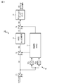
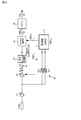
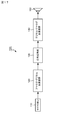
- FIG. 1 is a block diagram showing an outline of a system configuration of an analog-to-digital converter according to an embodiment of the present disclosure.
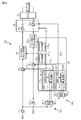
- FIG. 2 is a block diagram showing a specific circuit example of the analog-to-digital converter according to the embodiment of the present disclosure.
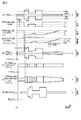
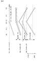
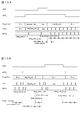
- FIG. 3 is a schematic schematic diagram showing changes in input / output signals and control signals at each point in the system of the analog-to-digital converter according to the embodiment of the present disclosure.
- FIG. 4 is a level diagram when the gain 0 dB of the variable gain amplifier is suitable for the maximum allowable input of the analog-to-digital converter.
- FIG. 5 is a level diagram when the gain> 0 dB of the variable gain amplifier is appropriate for the maximum allowable input of the analog-to-digital converter.
- FIG. 1 is a block diagram showing an outline of a system configuration of an analog-to-digital converter according to an embodiment of the present disclosure.
- FIG. 2 is a block diagram showing a specific circuit example of the analog-to
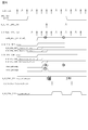
- FIG. 6 is a timing diagram for explaining the reason why the clock frequency of the timing generation unit of the ARC circuit and the control value generation unit is selected.
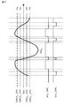
- FIG. 7 is a timing diagram showing the output signal of the energy comparator with respect to the output signal of the preamplifier.
- FIG. 8 is a block diagram showing a path from the variable gain amplifier to the digital attenuator.
- 9A and 9B are timing digrams showing an operation example of the gain setting of the variable gain amplifier.
- 10A and 10B are timing digrams showing operation examples of three timer counters that manage the processing intervals of the gain setting of the variable gain amplifier and the attenuation amount setting of the digital attenuator.
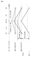
- FIG. 11 is an explanatory diagram of a delay time from the output of the audio signal from the preamplifier to the gain setting of the variable gain amplifier.
- FIG. 12 is an explanatory diagram of an implementation example of a 512 fs operation block.
- 13A and 13B are timing Daiguramu for explanation of the implementation example 1 of 128f s operation block.
- FIG. 14 is an explanatory diagram of the implementation example 2 of the 128 fs operation block.
- FIG. 15A is an explanatory diagram of a mounting example 3 of a 128 fs operation block, and FIG. 15B is a timing digram used for a description of the mounting example 3.
- FIG. 16 is a timing diagram showing an example of the operation of the delay timer in the implementation example 4 of the 128 fs operation block.
- FIG. 17 is a block diagram showing an outline of a system configuration of an audio device according to an embodiment of the present disclosure.
- Control unit 2-2-4 Input / output signals and control signals at each point in the system 2-2-5.
- Operating clock 2-2-6 Delay time due to analog-to-digital converter 2-2-7.
- About the delay of the gain setting operation of the variable gain amplifier 2-2-8 Setting the control timing difference between gain and attenuation 2-2-9.
- Implementation of delay for reflection of settings 2-2-10 Level interrupt and gain setting of variable gain amplifier 2-2-11. Setting the amount of attenuation 2-3. Control method, action, and effect according to the embodiment 2-4.
- the control method of the analog-to-digital converter, the audio device, and the whole may have a preamplifier that captures an input analog signal and supplies it to a variable gain amplifier. Then, the level detection unit can be configured to detect the level of the analog signal after passing through the preamplifier. Further, the level detection unit may be configured to have a plurality of comparators having different threshold values.
- a first level detector has a first threshold value higher than the bias of the output signal of the preamplifier. It is possible to have a comparator and a second comparator having a second threshold value lower than the bias of the output signal of the preamplifier. Then, for the first comparator, true logic is output when the level of the analog signal is higher than the first threshold value, and for the second comparator, the level of the analog signal is higher than the second threshold value. It can be configured to output true logic when it is low. Further, the level detection unit may be configured to output the logical sum of the output of the first comparator and the output of the second comparator as the detection level of the analog signal.
- the output impedance of the preamplifier is set with respect to the operation change of the variable gain amplifier and the level detector. It can be configured to have a constant role.
- the value of the control unit cancels out the attenuation of the attenuator and the gain of the variable gain amplifier. It can be configured to be controlled to. Further, the control unit can be configured to control the attenuation amount of the attenuator while maintaining a constant timing difference with respect to the control timing of the variable gain amplifier.
- the analog signal passed through the variable gain amplifier is oversampled and analog. It can be configured to consist of a delta-sigma modulator that converts the signal into a pulse train signal according to the amplitude of the signal.
- the signal of the pulse train output from the delta-sigma modulator and passed through the attenuator is aliased. It is possible to have a configuration having a decimation filter that converts a digital signal having a sampling frequency that can acquire necessary signal information without being affected by the above.
- FIG. 1 is a block diagram showing an outline of a system configuration of an analog-to-digital converter according to an embodiment of the present disclosure.
- An audio signal is input (microphone input).
- the analog-to-digital converter 10 includes a preamplifier 11, a variable gain amplifier 12, an analog-to-digital converter (ADC) 13, a digital attenuator 14, a decimation filter 15 which is an example of a digital filter, and a level detection unit 16. , And a control unit 17.
- the analog-to-digital converter 10 transfers the analog audio signal input through the preamplifier 11 to the variable gain amplifier 12, the analog-to-digital converter 13, the digital attenuator 14, and the decimation filter. It is output as an audio PCM (Pulse Code Modulation) signal via 15.
- PCM Pulse Code Modulation
- the preamplifier 11 has a variable gain, and the output impedance is made constant with respect to changes in the operation of the microphone in the front stage, the variable gain amplifier 12 in the rear stage, and the level detection unit 16. Has a role to play.
- the preamplifier 11 further sets an appropriate gain depending on the microphone (not shown) connected to the input side.
- the variable gain amplifier 12 is composed of, for example, a programmable gain amplifier (Programmable Gain Amp: PGA), and an analog audio signal input through the preamplifier 11 is set to the detection level of the level detection unit 16 under the control of the control unit 17. Amplifies with a gain (amplification amount) determined accordingly. Then, the variable gain amplifier 12 supplies the amplified analog audio signal to the next-stage analog-to-digital converter 13 operating in oversampling.
- PGA programmable gain amplifier
- variable gain amplifier 12 Under the control of the control unit 17, the variable gain amplifier 12 operates so that the gain becomes large when the microphone input level is small and the gain becomes small when the microphone input level is large.
- the gain increases slowly (for example, 0.2 dB step) with a gentle slope. Then, the step changes in a cycle of becoming a low frequency outside the audible band.
- the microphone input level changes from small to large, the gain drops instantly with a steep slope. As a result, it is possible to prevent incidental sounds in the entire frequency band that are generated even if the allowable input of the analog-digital converter 13 or the allowable output of the variable gain amplifier 12 is momentarily exceeded.
- the analog-digital converter 13 oversamples an analog signal (audio signal) amplified and input by the variable gain amplifier 12, and converts it into a pulse train signal (that is, a digital signal) according to the amplitude of the analog signal. It consists of a 1-bit delta-sigma modulator (hereinafter referred to as “ ⁇ modulator”).
- the digital attenuator 14 performs a process of attenuating the output of the analog-to-digital converter 13 operating in oversampling before decimation by the digital filter of the next stage. Specifically, the digital attenuator 14, under the control of the control unit 17, attenuates the digital audio signal output from the analog-digital converter 13 to cancel the amplification amount of the variable gain amplifier 12. Convert to the added value. When the number of bits of the output of the analog-to-digital converter 13 is 1 bit, the mapping of values is simple.
- the decimation filter 15 which is an example of a digital filter, is composed of, for example, a CIC (Cascaded Integrator Comb) filter.
- the decimation filter 15 converts the signal of the pulse train output from the analog-digital converter 13 and passed through the digital attenuator 14 into a digital signal having a sampling frequency that can acquire necessary signal information without being affected by aliasing noise. , Output as an audio PCM signal.
- the decimation filter 15 decimates according to the sampling frequency required by the circuit in the subsequent stage and outputs it as an audio PCM signal.
- Representative sampling frequency 4f s (f s: fundamental sampling frequency), 8f s, a 16f s.
- the input end of the level detection unit 16 is connected to the output end of the preamplifier 11 so as not to be affected by the impedance or the gain set in the preamplifier 11.
- the level detection unit 16 has x systems (2 systems in this example) of energy comparators 16 _1 and 16 _2 for n analog inputs.
- the two energy comparators 16 _1 and 16 _2 have different threshold values and detect the level of the analog audio signal after passing through the preamplifier 11.
- the energy comparator 16 _1 may be described as CMP _1 and the energy comparator 16 _2 may be described as CMP _2 .
- the control unit 17 is composed of, for example, an ARC (Adaptive Range Control) circuit, and controls the gain of the variable gain amplifier 12 and the amount of attenuation of the digital attenuator 14 based on the detection level of the level detection unit 16. Then, the control unit 17 accurately sets the control timing of the variable gain amplifier 12 and the control timing of the digital attenuator 14. This accurate control timing can be set from the fixed delay amount that can be determined by the topology of the analog-digital converter 13 and the input / output delay characteristics of the variable gain amplifier 12 whose fluctuation range is small even if variations are taken into consideration. it can.
- ARC Adaptive Range Control
- the analog-to-digital converter 10 detects the level of the input analog signal by the level detection unit 16, and based on the detection level, the gain of the variable gain amplifier 12 and the gain of the variable gain amplifier 12 and It has a feed-forward control configuration that controls the amount of attenuation of the digital attenuator 14.
- FIG. 2 is a block diagram showing a specific circuit example of the analog-to-digital converter according to the embodiment of the present disclosure.
- a circuit configuration in which a two-channel analog audio signal is input to the analog-to-digital converter 10 as MIC1 and MIC2 is illustrated.
- the analog-to-digital converter 10 includes preamplifiers 11 _1 and 11 _2 , variable gain amplifiers 12 _1 and 12 _2 , analog-to-digital converters 13 _1 and 13 _2 , and digital attenuators 14 _1 and 14 _2. ,
- the decimation filter 15 the energy comparators 16 _11 , 16 _12 , the energy comparators 16 _21 , 16 _22 , and the control unit 17.
- the variable gain amplifier 12 made of PGA has a gain set according to the digital value under the control of the control unit 17.
- the gain is controlled from 0 dB to 6 dB, for example, in steps of 0.2 dB. If the variable width of the gain that can be set is large, the dynamic range can be expected to be expanded by that amount, but since pop noise is noticeably generated, the practical variable width is preferably about 3 dB to 6 dB.
- the optimum gain of the variable gain amplifiers 12 _1 and 12 _2 is obtained according to the gains of the connected microphones and preamplifiers 11 _1 and 11 _2 , and the maximum allowable inputs of the analog-to-digital converters 13 _1 and 13 _2 .
- the purpose of this is to bring the outputs of the preamplifiers 11 _1 and 11 _2 closer to the maximum allowable inputs of the analog-to-digital converters 13 _1 and 13 _2 .
- Control unit 17 when the microphone input level is low, the variable gain amplifier 12 - 1, 12 gain _2 increases, when a large microphone input levels, the variable gain amplifier 12 - 1, so that the gain of 12 _2 decreases Be controlled.
- the analog-to-digital converter 10 is configured so that the gains of the preamplifiers 11 _1 and 11 _2 can be set in a range wider than the variable width of the dynamic range.
- the step width should be as small as possible.
- a typical example is 0.2 dB.
- the control unit 17 is provided with two ARC circuits 171 _1 and 171 _2 corresponding to two channels.
- the two ARC circuits 171 _1 and 171 _2 have timing generation units 171 _11 and 171 _21 and control value generation units 171 _12 and 171 _22 , respectively.
- the timing generator 171 _11 of the ARC circuit 171 _1 generates a timing signal T _1 that determines the timing for controlling the gain of the variable gain amplifier 12 _1 .
- the timing generator 171 _21 of the ARC circuit 171 _2 generates a timing signal T _2 that determines the timing for controlling the gain of the variable gain amplifier 12 _2 .
- the gain settings of the variable gain amplifiers 12 _1 and 12 _2 are generated by the control value generators 171 _12 and 171 _22 of the two ARC circuits 171 _1 and 171 _2 under the control of the control unit 17 having the above configuration. It is performed by the control values (set values) N _p1 and N _p2 . Further, the gain during the transition period is set to be an intermediate gain before and after the setting. Further, the setting of each attenuation amount of the digital attenuators 14 _1 and 14 _2 is controlled by the control unit 17 having the above configuration, and the control value generators 171 _12 and 171 of the two ARC circuits 171 _1 and 171 _2 are set. It is performed by the control values N _a1 and N _a2 generated in _22 .
- Analog - digital converter 13 _1, 13 _2, 128f s a (f s fundamental sampling frequency.44.1kHz / 48kHz ) in 1bit.
- the dither circuits 172 _1 and 172 _2 provided in the control unit 17 are also 1 bit.
- the preamplifiers 11 _1 and 11 _2 , the variable gain amplifiers 12 _1 and 12 _2 , the energy comparators 16 _11 and 16 _12 , and the energy comparators 16 _21 and 16 _22 are analog.
- the block is composed of the analog-to-digital converters 13 _1 and 13 _2 , the digital attenuators 14 _1 and 14 _2 , the decimation filter 15, and the control unit 17, and the control unit 17 constitutes the digital block.
- the analog-digital converters 13 _1 and 13 _2 and the dither circuits 172 _1 and 172 _2 in the digital configuration are analog. -The process is on the block side.
- 1 bit is illustrated at 128 fs for the operating speed and bit width of the analog-to-digital converters 13 _1 and 13 _2 , but the present invention is not limited to this.
- 64 fs or 128 fs may be 3 bits
- dither circuits 172 _1 , 172 _2 may be 2 bits
- the analog-digital converters 13 _1 and 13 _2 are not particularly limited.
- the circuit configuration of the digital attenuator 14 (14 _1 , 14 _2 ) will be described.
- this can be achieved by mapping to a fixed value according to the amount of attenuation. In this circuit example, it is mapped to 16 bits.
- the attenuation processing is realized by multiplication by a multiplier or by writing-type multiplication such as addition of the number of bits of the mapped value. it can.
- the same step amount as the gain step of the variable gain amplifier 12 is realized.
- the gain step of the variable gain amplifier 12 is 0.2 dB
- the maximum allowable value of the attenuation step is 0.2 dB.
- the step amount of the digital attenuator 14 is the same as the step amount of the variable gain amplifier 12, or one factorial of 2, 0.1 dB, 0.05 dB, 0.025 dB, ... Defined in.
- 0 dBFS of the output of the decimation filter 15 can be accurately defined.
- the output of the decimation filter 15 is operated with a bit width of a PCM signal having a wider dynamic range such as 24 bits or 32 bits, but the reference of the microphone input of multiple channels and the output of the analog-to-digital converter 13 are 0 dBFS (FS). : Full Scale) is effective when combined. It is not necessary to perform the multiplication process of level matching between a plurality of channels at a plurality of places. However, it is decided in consideration of the circuit scale.
- the energy comparators 16 _1 and 16 _2 output the truth of the comparison result with the comparison value depending on the energy.
- the input signal is detected by the energy comparator 16 _2 having the threshold value).
- the energy comparator 16 _1 on the side where the threshold value is higher than the bias outputs the true logic when the input is higher than the threshold value.
- the energy comparator 16 _2 on the side where the threshold value is lower than the bias outputs the true logic when the input is lower than the threshold value. Then, the logical sum of the outputs of these two energy comparators 16 _1 and 16 _2 becomes the energy comparison result. It is configured so that at least two energy thresholds can be set.
- An example of setting the energy threshold is as follows. That is, when the input level to the analog-to-digital converter 13 that the analog-to-digital converter 13 can output without distortion is 0 dB, the gain of the variable gain amplifier 12 is controlled and the lower limit of the variable width is set, the analog-digital The input level of the converter 13 is set to the output level of the preamplifier 11 which is -6 dB and -9 dB. The larger threshold value is equal to the reciprocal of the maximum gain set in the variable gain amplifier 12, and the next threshold value is set to a value 3 dB smaller than that.
- control unit 17 including the ARC circuit will be described.
- the control unit 17 treats the output signals of the two-level energy comparators 16 _1 and 16 _2 as priority asynchronous level interrupt signals, and controls the gain of the variable gain amplifier 12 according to the level interrupt signals.
- the control unit 17 further sets the amount of attenuation of the digital attenuator 14 according to the level interrupt signal.
- the control unit 17 controls the amount of attenuation of the digital attenuator 14 to a value that cancels out the gain of the variable gain amplifier 12 while always maintaining a constant timing difference with respect to the control timing of the variable gain amplifier 12.
- the control timing of the digital attenuator 14 is the theoretical delay clock cycle according to the configuration of the analog-to-digital converter 13, and the energy comparators 16 _1 and 16 _2 and the variable gain amplifier 12 are used. Generate by adding clock cycles for the time considering the difference in delay between input and output.
- the control unit 17 When the gain set value of the current variable gain amplifier 12 is higher than the gain set value of the target variable gain amplifier 12 determined in response to the level interrupt signal, the control unit 17 immediately changes the variable gain. Control the amplifier 12 to a low target gain. When the gain set value of the current variable gain amplifier 12 is lower than the gain set value of the target variable gain amplifier 12, the control unit 17 controls so that the slope does not change temporarily depending on the interrupt timing.
- the control unit 17 controls the gain of the variable gain amplifier 12 step by step while maintaining a slope of a constant gain change.
- the timing of stepwise control is longer than the period of frequencies lower than the audible band.
- the step period is set long, such as at 1-second intervals, noise generated by the spurious component due to the quantization of the analog-digital converter 13, which cannot be avoided depending on the number of bits of the analog-digital converter 13 and the configuration of the dither circuit. You may notice the phenomenon that the tone is attached to the digital. In that case, the step period is set to a period of a higher frequency outside the audible band, such as 300 ms.
- FIG. 3 is a schematic schematic diagram showing changes in input / output signals and control signals at each point in the system.
- the horizontal axis of FIG. 3 is time.
- the microphone input is an analog signal, but in FIG. 3, a step signal is given for easy understanding.
- (A) to (E) of FIG. 3 represent each waveform of each point (A) to (E) of FIG.
- the first stage is the output signal of the preamplifier 11, and represents the waveform of the input signal PGA in of the variable gain amplifier 12.
- the second stage is the target gain of the variable gain amplifier 12 set by the energy comparator 16 _1 and the energy comparator 16 _2 .
- the third stage is the gain set in the variable gain amplifier 12 by the control unit 17 composed of the ARC circuit.
- the fourth stage is the amount of attenuation set by the control unit 17 in the digital attenuator 14.
- the fifth stage is the output signal PGA out of the variable gain amplifier 12 in which the gain of the variable gain amplifier 12 of the third stage is reflected in the input signal PGA in of the variable gain amplifier 12 of the first stage, and is an analog-to-digital converter. It represents the waveform of the 13 input signals ADC in .
- the sixth stage represents the waveform of the signal ADC out after being converted into a PDM (Pulse Density Modulation) signal by the 1-bit analog-digital converter 13.
- PDM Pulse Density Modulation
- the seventh stage is a signal after the output signal ADC out of the analog-digital converter 13 has been attenuated by the attenuation amount of the fourth stage, and represents the waveform of the input signal CIC in of the decimation filter 15.
- the eighth stage finally represents the waveform of the signal MIC (CIC) out after being PCM-converted by the decimation filter 15.
- FIG. 4 is a level diagram in which the gain 0 dB of the variable gain amplifier 12 is suitable for the maximum allowable input of the analog-to-digital converter 13.
- the points (A) to (D) correspond to the points (A) to (D) in FIG.
- the threshold of the energy comparator 16 _1 (CMP _1 ) in FIGS. 4 and 5 is -6 dB of the maximum allowable input level
- the threshold of the energy comparator 16 _2 (CMP _2 ) is -9 dB of the maximum allowable input level.
- FIG. 5 shows that when the gain> 0 dB of the variable gain amplifier 12 is appropriate for the maximum allowable input of the analog-to-digital converter 13, in other words, when the gain of the variable gain amplifier 12 is 0 dB, the external input is analog-at the maximum. It is a level diagram when the input range of a digital converter 13 cannot be used effectively.
- the gain of the variable gain amplifier 12 is set to the minimum gain p min instead of 0 dB.
- 0 dBFS is set to the maximum value of the external input. This is a measure when the bit width of the audio PCM signal after being converted to PCM by the decimation filter 15 cannot be secured by about 24 bits and is not truncated.
- the preamplifiers 11 _1 and 11 _2 , the variable gain amplifiers 12 _1 and 12 _2 , the energy comparators 16 _11 and 16 _12 , and the energy comparators 16 _21 and 16 _22 are composed of analog circuits. There is.
- the other components are composed of digital circuits that require a clock supply during operation, and real-time performance without delay is required. Therefore, the source of the operating clock is common to all components. It consists of an interface that does not require asynchronous transfer for control other than interrupt detection.
- the sampling frequency f s is represented by 44.1 kHz or 48 kHz.
- the transmission frequency of the source vibration crystal oscillator is 512 fs , that is, 22.592 MHz or 24.576 MHz.
- the output side to which a digital-to-analog converter or digital amplifier is connected requires a crystal oscillator because clock jitter affects it.
- f s has a slightly higher frequency. 26 MHz and 32 MHz are often used in wireless systems and the like. These are treated as 512 fs , and the sampling frequency f s is treated as 50.78125 kHz or 62.5 kHz.
- Control value generation unit 171 _12 , 171 _22 128f s of the block ARC circuit 171 _1 , 171 _2 of the control unit 17.
- Block dither circuit of control unit 17 256f s RZ signal generation, 128f s NRZ signal generation 4.
- Digital attenuator 14 and a decimation filter 15 128f s ⁇ N (N : 2 or more when the calculator share)
- the timing diagram of FIG. 6 is used to explain the reason why the clock frequencies of the timing generators 171 _11 and 171 _21 of the ARC circuits 171 _1 and 171 _2 and the control value generators 171 _12 and 171 _22 are selected. I will explain.
- Variable gain amplifier 12 Only when the control value changes when the control values of the variable gain amplifiers 12 _1 and 12 _2 are set at the same frequency as the operating clocks of the analog-to-digital converters 13 _1 and 13 _2.
- the timing signal CHG for setting the control value is issued to.
- the timing signal CHG corresponds to the timing signals T _1 and T _2 in FIG. 2, and is generated by the timing generation units 171 _11 and 171 _21 .
- the timing signal CHG transitions to a high level when a change in the control value is detected, and always becomes a low level in the next cycle.
- variable gain amplifier 12 is generated so that the pulse width is half the minimum change width of the control value and the change point of the timing signal CHG does not overlap with the change point of the control value in the variable gain amplifier 12.
- Four times the sampling frequency of the analog-to-digital converters 13 _1 and 13 _2 is appropriate.
- -Energy comparators 16 _1 and 16 _2 are captured as level signals. Since it is an asynchronous input signal, a delay of two cycles at the longest of the synchronization clock occurs. For the synchronization clock, four times the sampling frequency of the analog-to-digital converters 13 _1 and 13 _2 is appropriate.
- the timing diagram of is shown.
- Variable gain amplifier 12 - 1, 12 - 2 after gain setting, the variable gain amplifier 12 - 1, 12 - 2 and an analog - digital converter 13 _1, timed to peculiar delay of 13 _2, ARC circuit 171 _1, in 171 _2
- the control value generators 171 _12 and 171 _22 output the amount of attenuation for correction as the control value MIC x _VOL.
- the control value MICx_VOL corresponds to the control values N _a1 and N _a2 in FIG.
- Digital attenuator 14 _1, 14 _2 interprets the minimum gain p min the set value of the CMP _1 _VOL, the variable gain amplifier 12 - 1, 12 control the gain of _2 when set to minimum gain p min value MIC x Control so that _VOL is 0 dB.
- the interface between the ARC circuits 171 _1 and 171 _2 and the digital attenuators 14 _1 and 14 _2 is not the amount of attenuation, but the volume value that maps the negative gain in 0.05 dB steps.
- MIC x _VOL + PGA_VOL CMP _1 _VOL Is the relationship.
- the control unit 17 controls the gain of the variable gain amplifiers 12 _1 and 12 _2 and the amount of attenuation of the digital attenuators 14 _1 and 14 _2 at appropriate time intervals.
- FIG. 8 shows the path from the variable gain amplifier 12 (12 _1 , 12 _2 ) to the digital attenuator 14 (14 _1 , 14 _2 ).
- the delay time by the analog-to-digital converter 13 (13 _1 , 13 _2 ) is uniquely determined by the topology.
- the STF (f) (STF: Signal Transfer Function) can be obtained from the circuit, and the delay time ⁇ t can be obtained by arg (STF (f)) / 2 ⁇ f. f is calculated as 20 kHz.
- the operating clock of the control unit 17 is 512 fs , it may be converted by the number of cycles by the 512 fs clock, but the accuracy does not reach 512 fs because it varies in the analog unit, and the control unit including timing adjustment.
- the 17 main body operates at 128 fs , which is the same frequency as the analog-digital converter 13. As an example, in the case of a third-order delta-sigma modulator, 128 fs has 8.4 cycles.
- variable gain amplifier 12 (12 _1 , 12 _2 ) is an analog block, there is a delay variation, but in the actual design, it is possible to accommodate the delay in about one cycle of the 128 fs clock. Further, although it depends on the gain of the variable gain amplifier 12, when the gain range of the variable gain amplifier 12 is about 0 to 6 dB, the delay can be kept within the range of 2 to 4 cycles of the 128 fs clock, so that the delay is delayed. The variation is corrected by a fixed number of cycles.
- the delay setting cycle is variable. Since the change from large gain to small gain has a large step and is performed immediately, the delay value with the smaller gain is used for correction. Since the change from small gain to large gain is performed very slowly in small steps such as 0.2 dB, the control value of the current variable gain amplifier 12 is corrected with an appropriate delay value.
- the difference between the number of correction steps at 0 dB and 6 dB is about 1.5, so the correction step value when the gain changes from small to large and the correction step value when the gain changes from large to small It is possible to operate with only two.
- the delay of the variable gain amplifier 12 is shown in Table 1.
- the variable gain amplifier 12 gain f s frequency for (PGA gain), the minimum cycle (Min.cycle), usually cycle (Typ.cycle), the relationship of the maximum cycle (Typ.cycle) (delay of the variable gain amplifier 12 128 fs cycle) is shown in Table 2. Since there is a change by the operation clock frequency, the correction value cycle number refers to the register values that define the f s in the entire system to be able to change.
- the delay common cycle 8 of the ⁇ modulator is subtracted so that it can be set separately.
- the attenuation setting is small ⁇ large, 3 cycles other than the delay of the delta-sigma modulator
- the attenuation setting is large ⁇ small, 4 cycles other than the delay of the delta-sigma modulator
- the delay of the ⁇ modulator is delayed by 8 cycles and the delay of the variable gain amplifier 12 is added up, and then the attenuation of the digital attenuator 14 is set. For implementation reasons, when inserting a pipeline, reduce the recommended register setting by the number of cycles in the pipeline.
- the shift register is used to delay the number of flip-flops, the number of flip-flops is 100, which is a 1k gate scale. If it is realized by the time constant of the low-pass filter, the gate clock is not inferred, and unless the HALT function and the HALT clock configuration are used, the multiplication / addition circuit always operates and the power consumption is wasted.
- the gain of the variable gain amplifier 12 and the attenuation of the digital attenuator 14 are set with a difference of about 0.025 seconds, so even if the operating clock frequency is 128 fs , the cycle is performed. There is room in the number.
- the transition interval of the FSM Finite State Machine
- the transition interval of the FSM can be made slower than the processing interval of the gain setting of the variable gain amplifier 12 and the attenuation setting of the digital attenuator 14.
- three timer counters that manage the processing interval of the gain setting of the variable gain amplifier 12 and the attenuation amount setting of the digital attenuator 14 are prepared and mounted by FSM. ..
- FIGS. 9A and 9B show the output signal of the energy comparator 16 _1 (CMP _1 ), the output signal of the energy comparator 16 _2 (CMP _2 ), the target gain of the variable gain amplifier 12, and the gain of the variable gain amplifier 12. It shows PVOL.
- 10A and 10B show timing digrams of operation examples of three timer counters that manage the processing intervals of the gain setting of the variable gain amplifier 12 and the attenuation amount setting of the digital attenuator 14.
- 10A and 10B show the output signal of CMP _1 , the output signal of CMP _2 , the target gain of the variable gain amplifier 12, the gain PVOL of the variable gain amplifier 12, and the attenuation amount MVOL of the digital attenuator 14. ..
- the timing to lower the gain PVOL of the variable gain amplifier 12 is immediate.
- the timing interval for increasing the gain PVOL of the variable gain amplifier 12 is controlled to be always constant.
- the delay in setting the gain PVOL of the variable gain amplifier 12 and the setting of the attenuation amount MVOL of the digital attenuator 14 is also controlled so that the timing is not other than the setting, in other words, the time difference is constant.
- CMP _1 The output signal of the energy comparator 16 _1 (CMP _1 ) and the output signal of the energy comparator 16 _2 (CMP _2 ) are treated as level interrupts.
- the two interrupts are asynchronously switched at a clock of 512 fs , and then each enable register determines whether or not to use the interrupt.
- CMP _1 is preferentially processed as a priority interrupt.
- the gain setting register CMP x _VOL of the variable gain amplifier 12 that sets a large amount of power in the threshold setting register CMP n H x _VTH of CMP _1 and sets it when processing an interrupt request has a smaller gain toward CMP _1.
- a set value register is prepared for each of the analog input system n and the energy comparator system x.
- the gain of the variable gain amplifier 12 is immediately set to the value of the setting register. 2.
- the gain of the variable gain amplifier 12 is asymptotically approached to the target value at intervals set in a predetermined register.
- the gain step of the variable gain amplifier 12 that transitions at one time is usually 0.2 dB.
- the set value is variable.
- the gain of the variable gain amplifier 12 is the actual value obtained by multiplying the register value by an integer and multiplying it by 0.2.
- the upper and lower limits of the gain setting of the variable gain amplifier 12 can be set.
- the lower limit of the gain setting is set on the assumption that the input range of the analog-digital converter 13 cannot be used up even if the maximum input of the external microphone passes through the preamplifier 11. Even at the maximum input, it is possible to use with + 3 dB gain instead of + 6 dB gain. Let this value be the minimum gain p min .
- the upper limit of the gain setting assumes that the noise figure of the variable gain amplifier 12 when the gain is high is bad, and the S / N during normal operation may be worsened in the entire system. Corresponds when it is better to use at + 4 dB than at + 6 dB. Let this value be the maximum gain p max .
- FIG. 11 shows an explanatory diagram of the delay time from the output of the audio signal from the preamplifier 11 to the gain setting of the variable gain amplifier 12.
- An example of the delay amount of the energy comparators 16 _1 and 16 _2 is 0.4 ⁇ s.
- the level interrupt is asynchronously switched by the fastest clock in the system and the fastest clock synchronized with the operating clock of the control unit 17.
- the delay from the comparison determination of the input levels of the ARC circuits 171 _1 and 171 _2 of the control unit 17 to the gain setting of the variable gain amplifier 12 is the sum of these.
- the operation clock 128f s a source oscillation of 1/4 of the speed of the control unit 17, 16 _1, 10 cycle delay is generated from the output 16 _2 from 6 cycles of 512f s clock. Since the time is 0.666 ⁇ s to 0.834 ⁇ s, the delay in this part is ignored.
- the amount of attenuation of the digital attenuators 14 _1 and 14 _2 is set by the minimum gain p min and the gain setting values p vol of the variable gain amplifiers 12 _1 and 12 _2 .
- the gain set value p vol corresponds to the control values N _p1 and N _p2 in FIG.
- the attenuation matt p vol- p min Will be.
- the magnitude relationship between the minimum gain p min , the gain set value p vol , and the maximum gain p max is p min ⁇ p vol ⁇ p max Is.
- Table 3 shows an example of the setting specifications of the register MIC_VOL that controls the digital attenuators 14 _1 and 14 _2 .
- the register MIC_VOL is provided in the control value generation units 171 _12 and 171 _22 of FIG. Mute and 0 dB settings are anomalous.
- a negative volume representation m vol is output to the digital attenuators 14 _1 and 14 _2 by regular calculation using the gain setting values p vol of the variable gain amplifiers 12 _1 and 12 _2 .
- 0.2 or 0.05 is expressed as a fixed decimal number in binary as it is, it becomes an irrational number, so it is converted to an integer and treated.
- the minimum unit of the step of the gain set value p vol is 0.2 dB, which is four times the step of the negative volume representation m vol .
- p vol, p min, an integer value P VOL the p max was 5-fold, respectively, P MIN, the result of calculation with the P MAX, further 4 times the value M VOL digital attenuator 14 _1, 14 _2 It becomes the signal level to be supplied. Interfaces except for the sign bit, which is the most significant bit of M VOL .
- the integer values P VOL , P MIN , and P MAX are the same as the output signal and register set values.
- the amount of attenuation can be set finer than 0.2 dB in order to make adjustments on a channel-by-channel basis. Since the attenuation amounts of the digital attenuators 14 _1 and 14 _2 are fixed amounts, offsets can be given independently.
- the analog-to-digital converter 10 detects the level of the input analog signal, and based on the detection level, the gain of the variable gain amplifier 12 and the attenuation of the digital attenuator 14. It has a feed-forward control configuration that controls the amount. Further, the feedforward control can provide an analog-to-digital conversion device having excellent responsiveness of the control loop as compared with the feedback control.
- the following actions and effects can be obtained.
- -In audio applications it is possible to obtain a dynamic range during operation that is wider than the input dynamic range of the analog-to-digital converter 13 (13 _1 , 13 _2 ).
- -It is possible to sufficiently suppress the generation of pop noise, which is a problem in audio, in response to sudden strong input changes.
- a constant static characteristic can be obtained without affecting the input signal from the system.
- the dynamic range can be expanded without discomfort when changing from strong input to weak input.
- FIG. 12 is a diagram illustrating an implementation example of a 512 fs operation block.
- the inputs A_W_AIN n _CMP x of the energy comparators 16 _1 and 16 _2 are synchronized with a simple synchronization circuit and output as a level interrupt signal AIN n _CMP x .
- the FSM operating at a clock of 128 fs prompts data transition at intervals of 32 cycles or more. Therefore, the chattering removal of the level interrupt signal may be controlled by the FSM, and the input stage does not need to be dealt with.
- the synchronized signal asserts at the fastest speed even when the interrupt is asserted.
- the gain setting of the variable gain amplifiers 12 _1 and 12 _2 is realized by asserting the setting signal A_W_PGA x _CHG after giving the gain setting value A_W_PGA x _VOL.
- the 512f s operation block constituting a dedicated FSM to generate a setting signal A_W_PGA x _CHG.
- the state After the asynchronous reset is released from the RESET state, the state unconditionally transitions to the IDLE state. With this configuration, the most significant bit side of the 2-bit register holding the state value is output as a signal for setting the gain values of the variable gain amplifiers 12 _1 and 12 _2 .
- 13A and 13B are timing Daiguramu illustrating the implementation example 1 of 128f s operation block.
- the target gain setting value is set according to the priority interrupt signal and the interrupt used at the input of the FSM.
- the target gain set value is used to generate the gain PVOL of the variable gain amplifiers 12 _1 and 12 _2 .
- the gain PVOL is managed inside the FSM and outputs a value to be set.
- the delay control of the gain setting timing and the attenuation setting timing is configured by three delay timers.
- Each delay timer starts operation with a start signal, and when it reaches a predetermined set threshold value, it generates an attenuation setting signal from the gain set value.
- the three delay timers are the delay timer 1 that starts operation when the energy comparator CMP 1 asserts, the delay timer 2 that starts operation when only the energy comparator CMP 2 asserts, and the asserted states of the energy comparators CMP 1 and CMP 2 . It is composed of a delay timer 3 that starts operation at a timing when the target gain set value determined in is set lower than the current gain set value.
- the gain setting value set when the energy comparators CMP 1 and CMP 2 are asserted is constant. It is variable depending on the register.
- the target gain set value PVOL 1 set when the energy comparator CMP 1 referenced by the delay timer 1 asserts is the minimum gain p min .
- the set value is stored in the AIN x _CMP 1 _VOL register and supplied as the signal name CSYN_AIN x CMP 1 _VOL.
- the target gain set value PVOL 2 set when the energy comparator CMP 2 referenced by the delay timer 2 asserts is an intermediate gain, and the set value is stored in the AIN x _CMP 2 _VOL register, and CSYN_AIN x CMP 2 Supplied as _VOL.
- the target gain set value referred to by the delay timer 3 is the currently set gain value PVOL.
- the attenuation set value MVOL is generated as the signal name A_M_MIC x _VOL.
- the attenuation set value MVOL determines the amplitude of the input signal of the digitalization filter 15.
- FIG. 14 is a diagram illustrating an implementation example 2 of a 128 fs operation block.
- the implementation example 2 is an implementation example in which the gain set value PVOL (A_W_PGA x _VOL) is forcibly set to a fixed value. Normally, the set value is controlled by the FSM, but it is reflected when the enable asserts the values of the fixed setting register PGA x _VOL and the signal name CSYN_PGA x _VOL.
- FIG. 15A is an explanatory diagram of a mounting example 3 of a 128 fs operation block
- FIG. 15B is a timing digram used for a description of the mounting example 3.
- Implementation example 3 is an implementation example of FSM.
- This counter controls the FSM. It is an implementation that increments when the value is other than 0. This counter controls the FSM operation that changes the gains of the variable gain amplifiers 12 _1 and 12 _2 at regular intervals when the target gain set value is larger than the current gain set value PVOL.
- FSM operates when the CSYN_ARC x _EN signal is asserting. You are in the RESET (0) state when negating. When the CSYN_ARC x _EN signal is asserted, the state transitions from the SETET (0) state to the EQUAL (1) state.
- the state In the EQUAL (1) state, the state remains in the EQUAL (1) state when the gain set value PVOL is equal to the target gain set value.
- the gains of the variable gain amplifiers 12 _1 and 12 _2 are set at regular timings.
- the FSM control counter It transitions to the LESS_THAN (2) state, and at the same time, sets the FSM control counter to 1 and starts incrementing.
- the FSM control counter reaches 32, the state transitions to the INTERVAL (3) state.
- the INTERVAL (3) state the FSM control counter is observed to create a time interval in which the gain set value is stepped up in the unit set in the ARC x PGA_STEP register, usually equivalent to 0.2 dB.
- the timing can be created by comparing only the high-order bits, ignoring the low-order bits of the counter that operates at the FSM operating clock of 128 fs .
- the threshold value for comparison with the high-order bit of the counter is set by the ARC n TIMER_TH register and the signal name CSYN_ARC n TIMER_TH.
- the gain set value PVOL is updated to a step-up value.
- the increment operation of the delay timer 3 for operating the attenuation set value MVOL with a delay difference is started, and the PVOL3 register for notifying the update value to the circuit for generating the attenuation set value MVOL is gained.
- Set value Set to the same value as PVOL.
- the gain of the variable gain amplifiers 12 _1 and 12 _2 is set as the target value in the next cycle in any state, and EQUAL is set. (1) Transition to the state.
- the increment operation of the delay timer 1 or the delay timer 2 for controlling the digital attenuators 14 _1 and 14 _2 is started.
- a start signal is generated at the start of the increment operation of the delay timer 1 / delay timer 2.
- This logic can be realized by the fact that the current gain setting value is larger than the target gain setting value. This is because the current gain setting value is always equal to the target gain setting value in the next cycle.
- the counter for FSM control is also set to 0 to stop the operation.
- Both delay timers are incremented by a value other than 0, set to 1 in the next cycle when the start signal is asserted, and set to 0 when the threshold is reached.
- Implementation example 4 is an operation example of the delay timer.
- FIG. 16 shows an example of a timing diagram of the operation of the delay timer. Here, it is defined on the premise that the threshold value of the delay timer does not exceed 31.
- the timing diagram of FIG. 16 shows the time when the threshold value of the delay timer is the maximum set value 31.
- the threshold of the delay timer is a maximum of 12 cycles with a 128 fs ⁇ modulator prepared as specified in the above section (setting the control timing difference between gain and attenuation), and a ⁇ modulator with the same topology at 64 fs . Even when it is operated, the delay cycle by the ⁇ modulator is 16, so the maximum is 20 cycles. Therefore, a setting of 31 is sufficient for the threshold of the delay timer.
- the delay timer changes three different gain settings due to an event at a timing different from the FSM that occurs to transition the two gain setting values to the lower side and an event due to one FSM that shifts the gain setting value to the higher side. From a point, it is a circuit for making a change point of digital attenuators 14 _1 and 14 _2 by a small-scale circuit operation.
- an attenuation setting value suitable for each event is generated at the timing when one of the delay timers reaches the threshold value. Since the attenuation set value is calculated from the gain set value, the appropriate gain set values PVOL 1 , PVOL 2 , and PVOL 3 are referred to for each timing separately from the current gain set value. It occurs at independent timings, and in the above section (About the delay of the gain setting operation of the variable gain amplifier), the delay time is defined not by gain but by the direction of change of the gain setting. It stipulates. This makes the number of delay cycles of the delay timer 1 and the delay timer 2 the same, and guarantees that the time until the threshold is reached never fluctuates.
- the setting delay is in units of 128 fs, the perception of error can be ignored, and this is a limitation applied for the premise of lightening the implementation. Since the gain setting value change generated by the interrupt from the energy comparators 16 _1 and 16 _2 may occur while the delay timer 3 is operating, the condition for stopping the delay timer 3 is the delay timer 1 or the delay timer 2. Includes the timing when the threshold is reached.
- the threshold value of the delay timer 3 is reached at the same time as the threshold value of the delay timer 1 or the delay timer 2, the threshold arrival of the delay timer 1 or the delay timer 2 is prioritized, so that the variable gain amplifiers 12 _1 and 12 _2 Immediately effective operation of gain change can be preferentially executed even by controlling the digital attenuators 14 _1 and 14 _2 .
- the operation of the delay timer also determines the priority of the setting timing of the attenuation set values set in the digital attenuators 14 _1 and 14 _2. Therefore, the registers holding the attenuation set values are the respective delay timers. It is possible to configure a circuit that determines the value by referring to the values of the gain set values PVOL 1 , PVOL 2 , and PVOL 3 according to the delay timer at the arrival timing of, without considering the priority.
- the generation of the attenuation set value MVOL is determined by the calculation formula defined in the above-mentioned (Attenuation setting) section, and overflow processing is also performed.
- the threshold arrival timing of the delay timer is notified one cycle earlier, and the selection of the gain setting values PVOL 1 , PVOL 2 , and PVOL 3 for generating the attenuation set value MVOL is confirmed one cycle earlier and held in the pipeline. .. Therefore, as defined in the above-mentioned section (setting the control timing difference between the gain and the attenuation amount), a value one cycle smaller is given to the setting register that controls the threshold value of the delay timer.
- the analog-to-digital conversion device 10 according to the embodiment of the present disclosure described above can be used as the analog-to-digital conversion device in various audio devices including the analog-digital conversion device.
- FIG. 17 is a block diagram showing an outline of a system configuration of an audio device according to the embodiment of the present disclosure using the analog-digital conversion device 10 according to the embodiment of the present disclosure.
- the audio device 100 according to the present embodiment is configured to include, for example, a microphone 110, an analog-to-digital conversion device 120, a signal processing unit 130, a digital-analog conversion device 140, and a speaker 150.
- the analog-to-digital conversion device 10 can be used as the analog-to-digital conversion device 120 that converts the analog audio signal input from the microphone 110 into an audio PCM signal. it can. Since the analog-to-digital converter 10 is a feed-forward control that detects the level of the input analog audio signal and performs gain control based on the detection level, the analog-to-digital converter 120 is a control loop. It is possible to realize an analog-to-digital converter with excellent responsiveness.
- analog-digital conversion device 10 is applied to the audio device 100 has been described as an example, but the application is not limited to the audio device.
- an analog-digital converter (delta-sigma modulation type analog-digital converter) composed of a ⁇ modulator is used as the analog-digital converter 13 in the analog-digital converter 10.
- the present invention is not limited to this, and other forms of analog-to-digital converters such as delta-sigma analog-to-digital converters can be used.
- the present disclosure may also have the following configuration.
- Analog-to-digital converter [A-1] A variable gain amplifier that amplifies the input analog signal, An analog-to-digital converter that converts an analog signal that has passed through a variable gain amplifier into a digital signal, Attenuator that attenuates the digital signal output from the analog-to-digital converter, Level detector that detects the level of analog signals, and A control unit for controlling the gain of the variable gain amplifier and the amount of attenuation of the attenuator based on the detection level of the level detection unit is provided. Analog-to-digital converter. [A-2] It has a preamplifier that takes in the input analog signal and supplies it to the variable gain amplifier. The level detector detects the level of the analog signal after passing through the preamplifier.
- the level detector has a plurality of comparators having different threshold values.
- the level detector has a first comparator having a first threshold value higher than the bias of the output signal of the preamplifier, and a second comparator having a second threshold value lower than the bias of the output signal of the preamplifier. Have a comparator, The analog-to-digital converter according to the above [A-3].
- the first comparator outputs true logic when the level of the analog signal is higher than the first threshold.
- the second comparator outputs true logic when the level of the analog signal is lower than the second threshold.
- the level detection unit outputs the logical sum of the output of the first comparator and the output of the second comparator as the detection level of the analog signal.
- the preamplifier has a role of making the output impedance constant with respect to the operation change of the variable gain amplifier and the level detector.
- the [A-8] control unit controls the amount of attenuation of the attenuator to a value that cancels the gain of the variable gain amplifier.
- the analog-to-digital converter according to any one of the above [A-1] to the above [A-7].
- the control unit controls the amount of attenuation of the attenuator while maintaining a constant timing difference with respect to the control timing of the variable gain amplifier.
- the analog-to-digital converter consists of a delta-sigma modulator that oversamples an analog signal that has passed through a variable gain amplifier and converts it into a pulse train signal according to the amplitude of the analog signal.
- the analog-to-digital converter according to any one of the above [A-1] to the above [A-9].
- [A-11] It has a decimation filter that converts a pulse train signal output from a delta-sigma modulator and passed through an attenuator into a digital signal having a sampling frequency that can acquire necessary signal information without being affected by aliasing noise.
- [B-2] Converts the pulse train signal output from the delta-sigma modulator, passed through the attenuator, into a digital signal with a sampling frequency that can acquire the necessary signal information without being affected by aliasing noise.
- Audio equipment [C-1] Variable gain amplifier that amplifies the input analog signal, An analog-to-digital converter that converts an analog signal that has passed through a variable gain amplifier into a digital signal, Attenuator that attenuates the digital signal output from the analog-to-digital converter, Level detector that detects the level of analog signals, and A control unit for controlling the gain of the variable gain amplifier and the amount of attenuation of the attenuator based on the detection level of the level detection unit is provided.
- An audio device having an analog-to-digital converter.
- It has a preamplifier that takes in the input analog signal and supplies it to the variable gain amplifier. The level detector detects the level of the analog signal after passing through the preamplifier.
- the level detector has a plurality of comparators having different threshold values.
- the level detector has a first comparator having a first threshold value higher than the bias of the output signal of the preamplifier, and a second comparator having a second threshold value lower than the bias of the output signal of the preamplifier. Have a comparator, The audio device according to the above [C-3].
- the first comparator outputs true logic when the level of the analog signal is higher than the first threshold.
- the second comparator outputs true logic when the level of the analog signal is lower than the second threshold.
- the [C-6] level detection unit outputs the logical sum of the output of the first comparator and the output of the second comparator as the detection level of the analog signal.
- the preamplifier has a role of making the output impedance constant with respect to the operation change of the variable gain amplifier and the level detector.
- the [C-8] control unit controls the amount of attenuation of the attenuator to a value that cancels the gain of the variable gain amplifier.
- the [C-9] control unit controls the amount of attenuation of the attenuator while maintaining a constant timing difference with respect to the control timing of the variable gain amplifier.
- the audio device according to [C-8].
- the analog-to-digital converter consists of a delta-sigma modulator that oversamples an analog signal that has passed through a variable gain amplifier and converts it into a pulse train signal according to the amplitude of the analog signal.
- the audio device according to any one of the above [C-1] to the above [C-9].
Landscapes
- Engineering & Computer Science (AREA)
- Theoretical Computer Science (AREA)
- Physics & Mathematics (AREA)
- Acoustics & Sound (AREA)
- Signal Processing (AREA)
- Analogue/Digital Conversion (AREA)
- Circuit For Audible Band Transducer (AREA)
- Compression, Expansion, Code Conversion, And Decoders (AREA)
- Control Of Amplification And Gain Control (AREA)
- Amplifiers (AREA)
Abstract
本開示のアナログ-デジタル変換装置は、入力されるアナログ信号を増幅する可変利得アンプ、可変利得アンプを経たアナログ信号をデジタル信号に変換するデジタル-アナログ変換器、デジタル-アナログ変換器から出力されるデジタル信号を減衰させる減衰器、入力されるアナログ信号のレベルを検出するレベル検出部、及び、レベル検出部の検出結果に基づいて、可変利得アンプの利得入力される、及び、減衰器の減衰量を制御する制御部を備える。
Description
本開示は、アナログ-デジタル変換装置、アナログ-デジタル変換装置の制御方法、及び、オーディオ装置に関する。
種々のオーディオ装置において、マイクロホン等から入力されるアナログのオーディオ信号をデジタル信号に変換するために、アナログ-デジタル変換装置が用いられている。S/Nやダイナミックレンジを最大限に確保するために、オーディオ装置に用いられる、従来のアナログ-デジタル変換装置は、マイク出力特性に応じて静的利得でアナログ-デジタル変換器の入力前段にてレベル調整し、アナログ-デジタル変換器の後段に配されたデシメーションフィルタの出力レベルを調整するようにしていた(例えば、特許文献1参照)。特許文献1には、アナログ-デジタル変換装置のデルタ-シグマ変調器のフィードバックを改良することで、純粋に特性を改善する技術も開示されている。
また、オーディオ装置に用いられる、従来のアナログ-デジタル変換装置では、アナログ-デジタル変換器の後段に配されたデシメーションフィルタの出力レベルを検出し、その検出レベルを、アナログ-デジタル変換器の前段に配された可変利得アンプにフィードバックし、当該可変利得アンプの利得を制御するようにしていた(例えば、特許文献2参照)。
また、オーディオ装置に用いられる、従来のアナログ-デジタル変換装置では、アナログ-デジタル変換器の後段に配されたデシメーションフィルタの出力レベルを検出し、その検出レベルを、アナログ-デジタル変換器の前段に配された可変利得アンプにフィードバックし、当該可変利得アンプの利得を制御するようにしていた(例えば、特許文献2参照)。
特許文献1に記載の従来技術に係るアナログ-デジタル変換装置は、デルタ-シグマ変調器のフィードバック部を改良することで歪み特性を改善して許容入力レベルを引き上げているが、デルタ-シグマ変調器の特性変更が困難である、という問題がある。
特許文献2に記載の従来技術に係るアナログ-デジタル変換装置は、フィードバック制御であるために、信号レベルに応じて可変利得アンプの利得を制御する制御ループの応答性が遅い。具体的には、アナログ-デジタル変換器の処理遅延、デシメーションフィルタの処理遅延、及び、レベル検出回路の処理遅延が存在する分だけ制御ループの応答性が遅い。このように、特許文献2に記載の従来技術では、制御ループの応答性が遅く、ノイズキャンセルに必要な応答性を保証できない、という問題がある。
特許文献2に記載の従来技術に係るアナログ-デジタル変換装置は、フィードバック制御であるために、信号レベルに応じて可変利得アンプの利得を制御する制御ループの応答性が遅い。具体的には、アナログ-デジタル変換器の処理遅延、デシメーションフィルタの処理遅延、及び、レベル検出回路の処理遅延が存在する分だけ制御ループの応答性が遅い。このように、特許文献2に記載の従来技術では、制御ループの応答性が遅く、ノイズキャンセルに必要な応答性を保証できない、という問題がある。
本開示は、信号レベルに応じて可変利得アンプの利得を制御する制御ループの応答性に優れたアナログ-デジタル変換装置、アナログ-デジタル変換装置の制御方法、及び、オーディオ装置を提供することを目的とする。
上記の目的を達成するための本開示のアナログ-デジタル変換装置は、
入力されるアナログ信号を増幅する可変利得アンプ、
可変利得アンプを経たアナログ信号をデジタル信号に変換するアナログ-デジタル変換器、
アナログ-デジタル変換器から出力されるデジタル信号を減衰させる減衰器、
入力されるアナログ信号のレベルを検出するレベル検出部、及び、
レベル検出部の検出レベルに基づいて、可変利得アンプの利得、及び、減衰器の減衰量を制御する制御部を備える。
入力されるアナログ信号を増幅する可変利得アンプ、
可変利得アンプを経たアナログ信号をデジタル信号に変換するアナログ-デジタル変換器、
アナログ-デジタル変換器から出力されるデジタル信号を減衰させる減衰器、
入力されるアナログ信号のレベルを検出するレベル検出部、及び、
レベル検出部の検出レベルに基づいて、可変利得アンプの利得、及び、減衰器の減衰量を制御する制御部を備える。
上記の目的を達成するための本開示のアナログ-デジタル変換装置の制御方法は、
入力されるアナログ信号を増幅する可変利得アンプ、
可変利得アンプを経たアナログ信号をデジタル信号に変換するアナログ-デジタル変換器、及び、
アナログ-デジタル変換器から出力されるデジタル信号を減衰させる減衰器を備えるアナログ-デジタル変換装置において、
入力されるアナログ信号のレベルを検出し、
その検出レベルに基づいて、可変利得アンプの利得、及び、減衰器の減衰量の制御を行う。
入力されるアナログ信号を増幅する可変利得アンプ、
可変利得アンプを経たアナログ信号をデジタル信号に変換するアナログ-デジタル変換器、及び、
アナログ-デジタル変換器から出力されるデジタル信号を減衰させる減衰器を備えるアナログ-デジタル変換装置において、
入力されるアナログ信号のレベルを検出し、
その検出レベルに基づいて、可変利得アンプの利得、及び、減衰器の減衰量の制御を行う。
また、上記の目的を達成するための本開示のオーディオ装置は、上記の構成のアナログ-デジタル変換装置を有する。
以下、本開示の技術を実施するための形態(以下、「実施形態」と記述する)について図面を用いて詳細に説明する。本開示の技術は実施形態に限定されるものではなく、実施形態における種々の数値などは例示である。以下の説明において、同一要素又は同一機能を有する要素には同一符号を用いることとし、重複する説明は省略する。尚、説明は以下の順序で行う。
1.本開示のアナログ-デジタル変換装置、アナログ-デジタル変換装置の制御方法、及び、オーディオ装置、全般に関する説明
2.本開示の実施形態に係るアナログ-デジタル変換装置
2-1.システム構成の概略
2-2.具体的な回路例
2-2-1.デジタル減衰器について
2-2-2.エネルギー比較器について
2-2-3.制御部について
2-2-4.システム内の各ポイントにおける入出力信号や制御信号について
2-2-5.動作クロックについて
2-2-6.アナログ-デジタル変換器による遅延時間について
2-2-7.可変利得アンプの利得設定動作の遅延について
2-2-8.利得と減衰量の制御タイミング差の設定について
2-2-9.設定反映の遅延の実装について
2-2-10.レベル割り込みと可変利得アンプの利得設定について
2-2-11.減衰量の設定について
2-3.実施形態に係る制御方法、及び、作用、効果
2-4.実装例
2-4-1.512fs動作ブロックの実装例
2-4-2.128fs動作ブロックの実装例1
2-4-3.128fs動作ブロックの実装例2
2-4-4.128fs動作ブロックの実装例3
2-4-5.128fs動作ブロックの実装例4
3.本開示の実施形態に係るオーディオ装置
4.変形例
5.本開示がとることができる構成
1.本開示のアナログ-デジタル変換装置、アナログ-デジタル変換装置の制御方法、及び、オーディオ装置、全般に関する説明
2.本開示の実施形態に係るアナログ-デジタル変換装置
2-1.システム構成の概略
2-2.具体的な回路例
2-2-1.デジタル減衰器について
2-2-2.エネルギー比較器について
2-2-3.制御部について
2-2-4.システム内の各ポイントにおける入出力信号や制御信号について
2-2-5.動作クロックについて
2-2-6.アナログ-デジタル変換器による遅延時間について
2-2-7.可変利得アンプの利得設定動作の遅延について
2-2-8.利得と減衰量の制御タイミング差の設定について
2-2-9.設定反映の遅延の実装について
2-2-10.レベル割り込みと可変利得アンプの利得設定について
2-2-11.減衰量の設定について
2-3.実施形態に係る制御方法、及び、作用、効果
2-4.実装例
2-4-1.512fs動作ブロックの実装例
2-4-2.128fs動作ブロックの実装例1
2-4-3.128fs動作ブロックの実装例2
2-4-4.128fs動作ブロックの実装例3
2-4-5.128fs動作ブロックの実装例4
3.本開示の実施形態に係るオーディオ装置
4.変形例
5.本開示がとることができる構成
<本開示のアナログ-デジタル変換装置、アナログ-デジタル変換装置の制御方法、及び、オーディオ装置、全般に関する説明>
本開示のアナログ-デジタル変換装置、その制御方法、及び、オーディオ装置にあっては、入力されるアナログ信号を取り込んで可変利得アンプに供給するプリアンプを有する構成とすることができる。そして、レベル検出部について、プリアンプを経た後のアナログ信号のレベルを検出する構成とすることができる。また、レベル検出部について、互いに異なる閾値を有する複数の比較器を有する構成とすることができる。
本開示のアナログ-デジタル変換装置、その制御方法、及び、オーディオ装置にあっては、入力されるアナログ信号を取り込んで可変利得アンプに供給するプリアンプを有する構成とすることができる。そして、レベル検出部について、プリアンプを経た後のアナログ信号のレベルを検出する構成とすることができる。また、レベル検出部について、互いに異なる閾値を有する複数の比較器を有する構成とすることができる。
上述した好ましい構成を含む本開示のアナログ-デジタル変換装置、その制御方法、及び、オーディオ装置にあっては、レベル検出部について、プリアンプの出力信号のバイアスよりも高い第1の閾値を有する第1の比較器、及び、プリアンプの出力信号のバイアスよりも低い第2の閾値を有する第2の比較器を有する構成とすることができる。そして、第1の比較器については、アナログ信号のレベルが第1の閾値よりも高いときに真の論理を出力し、第2の比較器については、アナログ信号のレベルが第2の閾値よりも低いときに真の論理を出力する構成とすることができる。また、レベル検出部について、第1の比較器の出力、及び、第2の比較器の出力の論理和を、アナログ信号の検出レベルとして出力する構成とすることができる。
また、上述した好ましい構成を含む本開示のアナログ-デジタル変換装置、その制御方法、及び、オーディオ装置にあっては、プリアンプについて、可変利得アンプ及びレベル検出器の動作変化に対して、出力インピーダンスを一定にする役割を持つ構成とすることができる。
また、上述した好ましい構成を含む本開示のアナログ-デジタル変換装置、その制御方法、及び、オーディオ装置にあっては、制御部について、減衰器の減衰量を、可変利得アンプの利得を相殺する値に制御する構成とすることができる。また、制御部について、減衰器の減衰量を、可変利得アンプの制御タイミングに対して一定のタイミング差を維持しながら制御する構成とすることができる。
また、上述した好ましい構成を含む本開示のアナログ-デジタル変換装置、その制御方法、及び、オーディオ装置にあっては、アナログ-デジタル変換器について、可変利得アンプを経たアナログ信号をオーバーサンプリングし、アナログ信号の振幅に応じたパルス列の信号に変換するデルタ-シグマ変調器から成る構成とすることができる。
また、上述した好ましい構成を含む本開示のアナログ-デジタル変換装置、その制御方法、及び、オーディオ装置にあっては、デルタ-シグマ変調器から出力され、減衰器を経たパルス列の信号を、折り返し雑音の影響を受けずに必要な信号情報を取得できるサンプリング周波数のデジタル信号に変換するデシメーションフィルタを有する構成とすることができる。
<本開示の実施形態に係るアナログ-デジタル変換装置>
図1は、本開示の実施形態に係るアナログ-デジタル変換装置のシステム構成の概略を示すブロック図である。本実施形態に係るアナログ-デジタル変換装置10には、外部の図示せぬマイクロホン(以下、単に「マイク」と記述する場合がある)から、n系統(図1では、n=1)のアナログのオーディオ信号が入力される(マイク入力)。
図1は、本開示の実施形態に係るアナログ-デジタル変換装置のシステム構成の概略を示すブロック図である。本実施形態に係るアナログ-デジタル変換装置10には、外部の図示せぬマイクロホン(以下、単に「マイク」と記述する場合がある)から、n系統(図1では、n=1)のアナログのオーディオ信号が入力される(マイク入力)。
[システム構成の概略]
本実施形態に係るアナログ-デジタル変換装置10は、プリアンプ11、可変利得アンプ12、アナログ-デジタル変換器(ADC)13、デジタル減衰器14、デジタルフィルタの一例であるデシメーションフィルタ15、レベル検出部16、及び、制御部17を有する構成となっている。
本実施形態に係るアナログ-デジタル変換装置10は、プリアンプ11、可変利得アンプ12、アナログ-デジタル変換器(ADC)13、デジタル減衰器14、デジタルフィルタの一例であるデシメーションフィルタ15、レベル検出部16、及び、制御部17を有する構成となっている。
アナログ-デジタル変換装置10は、制御部17による制御の下に、プリアンプ11を通して入力されるアナログのオーディオ信号を、可変利得アンプ12、アナログ-デジタル変換器13、デジタル減衰器14、及び、デシメーションフィルタ15を経由して、オーディオPCM(Pulse Code Modulation)信号として出力する。
上記の構成のアナログ-デジタル変換装置10において、プリアンプ11は、利得が可変であり、前段のマイクロホンや、後段の可変利得アンプ12及びレベル検出部16の動作変化に対して、出力インピーダンスを一定にする役割を持っている。プリアンプ11は更に、入力側に接続されるマイクロホン(図示せず)に応じて適切な利得を設定する。
可変利得アンプ12は、例えば、プログラマブル利得アンプ(Programmable Gain Amp:PGA)から成り、プリアンプ11を通して入力されるアナログのオーディオ信号を、制御部17による制御の下に、レベル検出部16の検出レベルに応じて決定される利得(増幅量)で増幅する。そして、可変利得アンプ12は、増幅したアナログのオーディオ信号を、オーバーサンプリングで動作している次段のアナログ-デジタル変換器13に供給する。
可変利得アンプ12は、制御部17による制御の下に、マイク入力レベルが小さいときに利得がとなり大、マイク入力レベルが大きいときに利得が小となるような動作になる。マイク入力レベルが大→小の変化時には、緩やかなスロープでゆっくり(例えば、0.2dBステップ)利得がアップする。そして、可聴帯域外の低い周波数になる周期でステップが変化する。マイク入力レベルが小→大 の変化時には、急峻なスロープで瞬時に利得がダウンする。これにより、アナログ-デジタル変換器13の許容入力や、可変利得アンプ12の許容出力を瞬間的に超えるだけでも発生する全周波数帯域の付帯音を防ぐことができる。
アナログ-デジタル変換器13は、例えば、可変利得アンプ12で増幅されて入力されるアナログ信号(オーディオ信号)をオーバーサンプリングし、アナログ信号の振幅に応じたパルス列の信号(即ち、デジタル信号)に変換する1bitのデルタ-シグマ変調器(以下、「ΔΣ変調器」と記述する)から成る。
デジタル減衰器14は、オーバーサンプリングで動作しているアナログ-デジタル変換器13の出力を、次段のデジタルフィルタでデシメーションする前に、減衰させる処理を行う。具体的には、デジタル減衰器14は、制御部17による制御の下に、アナログ-デジタル変換器13から出力されるデジタルのオーディオ信号を、可変利得アンプ12での増幅量を相殺する減衰量を加味した値に変換する。アナログ-デジタル変換器13の出力のビット数が1bitの場合は、単純な値のマッピングとなる。
デジタルフィルタの一例であるデシメーションフィルタ15は、例えば、CIC(Cascaded Integrator Comb:カスケード積分櫛形)フィルタから成る。このデシメーションフィルタ15は、アナログ-デジタル変換器13から出力され、デジタル減衰器14を経たパルス列の信号を、折り返し雑音の影響を受けずに必要な信号情報を取得できるサンプリング周波数のデジタル信号に変換し、オーディオPCM信号として出力する。
デシメーションフィルタ15は、後段の回路が要求するサンプリング周波数に合わせてデシメーションを行ってオーディオPCM信号として出力する。代表的なサンプリング周波数は、4fs(fs:fundamental sampling frequency),8fs,16fsである。
レベル検出部16は、インピーダンスやプリアンプ11に設定される利得による影響を受けないように、その入力端がプリアンプ11の出力端に接続される。レベル検出部16は、n系統のアナログ入力に対して、x系統(本例では、2系統)のエネルギー比較器16_1、16_2を有している。2系統のエネルギー比較器16_1、16_2は、互いに異なる閾値を有しており、プリアンプ11を経た後のアナログのオーディオ信号のレベルを検出する。以下、便宜上、エネルギー比較器16_1をCMP_1と記述し、エネルギー比較器16_2をCMP_2と記述する場合がある。
制御部17は、例えば、ARC(Adaptive Range Control)回路から成り、レベル検出部16の検出レベルに基づいて、可変利得アンプ12の利得、及び、デジタル減衰器14の減衰量を制御する。そして、制御部17は、可変利得アンプ12の制御タイミングとデジタル減衰器14の制御タイミングとを正確に設定する。この正確な制御タイミングについては、アナログ-デジタル変換器13のトポロジーで決定できる固定遅延量、及び、バラツキを加味しても変動幅が小さい可変利得アンプ12の入出力遅延の特性から設定することができる。
上述したように、本実施形態に係るアナログ-デジタル変換装置10は、入力されるアナログ信号のレベルをレベル検出部16で検出し、その検出レベルに基づいて、可変利得アンプ12の利得、及び、デジタル減衰器14の減衰量を制御するフィードフォワード制御の構成となっている。
[具体的な回路例]
図2は、本開示の実施形態に係るアナログ-デジタル変換装置の具体的な回路例を示すブロック図である。ここでは、例えば2チャンネルのアナログオーディオ信号が、MIC1及びMIC2としてアナログ-デジタル変換装置10に入力される場合の回路構成を例示している。
図2は、本開示の実施形態に係るアナログ-デジタル変換装置の具体的な回路例を示すブロック図である。ここでは、例えば2チャンネルのアナログオーディオ信号が、MIC1及びMIC2としてアナログ-デジタル変換装置10に入力される場合の回路構成を例示している。
従って、本回路例に係るアナログ-デジタル変換装置10は、プリアンプ11_1、11_2、可変利得アンプ12_1、12_2、アナログ-デジタル変換器13_1、13_2、デジタル減衰器14_1、14_2、デシメーションフィルタ15、エネルギー比較器16_11、16_12、エネルギー比較器16_21、16_22、及び、制御部17を有する構成となっている。
上記の回路例に係るアナログ-デジタル変換装置10において、PGAから成る可変利得アンプ12は、制御部17による制御の下に、デジタル値に応じて利得が設定される。本回路例では、0dBから6dBまで、例えば0.2dBステップで利得の制御が行われる。設定できる利得の可変幅が大きければ、その分だけ、ダイナミックレンジの拡大が期待できるが、ポップノイズの発生が顕著になるため、実用可変幅は3dB~6dB程度が好ましい。
接続されるマイクロホン、プリアンプ11_1,11_2の利得、及び、アナログ-デジタル変換器13_1、13_2の許容最大入力に応じて、可変利得アンプ12_1、12_2の最適利得が求められる。これは、プリアンプ11_1,11_2の出力を、アナログ-デジタル変換器13_1、13_2の許容最大入力に近づける目的である。制御部17は、マイク入力レベルが小さいときに、可変利得アンプ12_1、12_2の利得が大きくなり、マイク入力レベルが大きいときに、可変利得アンプ12_1、12_2の利得が小さくなるように制御される。
本実施形態に係るアナログ-デジタル変換装置10では、プリアンプ11_1,11_2の利得を、ダイナミックレンジの可変幅よりも広い範囲が設定できるように構成する。ステップ幅については、実現可能な範囲内で小さい値がよい。その代表例は0.2dBである。
制御部17には、2チャンネルに対応して2つのARC回路171_1、171_2が設けられている。2つのARC回路171_1、171_2はそれぞれ、タイミング生成部171_11、171_21及び制御値生成部171_12、171_22を有している。ARC回路171_1のタイミング生成部171_11は、可変利得アンプ12_1の利得を制御するタイミングを決めるタイミング信号T_1を生成する。ARC回路171_2のタイミング生成部171_21は、可変利得アンプ12_2の利得を制御するタイミングを決めるタイミング信号T_2を生成する。
ARC回路171_1の制御値生成部171_12は、可変利得アンプ12_1の利得を制御する制御値N_p1、及び、デジタル減衰器14_1の減衰量を制御する制御値N_a1を生成する。ARC回路171_2の制御値生成部171_22は、可変利得アンプ12_2の利得を制御する制御値N_p2、及び、デジタル減衰器14_2の減衰量を制御する制御値N_a2を生成する。
可変利得アンプ12_1、12_2の各利得の設定は、上記の構成の制御部17による制御の下に、2つのARC回路171_1、171_2の各制御値生成部171_12、171_22で生成される制御値(設定値)N_p1,N_p2によって行われる。更に、遷移期間中の利得については、設定前後の中間利得になるように設定される。また、デジタル減衰器14_1,14_2の各減衰量の設定は、上記の構成の制御部17による制御の下に、2つのARC回路171_1、171_2の各制御値生成部171_12、171_22で生成された制御値N_a1,N_a2によって行われる。
ここで、アナログ-デジタル変換器13_1、13_2の代表的な動作速度及びビット幅について説明する。アナログ-デジタル変換器13_1、13_2は、128fs(fs:fundamental sampling frequency.44.1kHz/48kHz)で1bitである。制御部17に設けられるディザ回路172_1、172_2についても1bitである。
上記の構成のアナログ-デジタル変換装置10において、プリアンプ11_1、11_2、可変利得アンプ12_1、12_2、エネルギー比較器16_11、16_12、及び、エネルギー比較器16_21、16_22は、アナログ・ブロックを構成し、アナログ-デジタル変換器13_1、13_2、デジタル減衰器14_1、14_2、デシメーションフィルタ15、及び、制御部17は、デジタル・ブロックを構成している。
尚、半導体プロセスとして、アナログ・ブロック側とデジタル・ブロック側とで異なるプロセスを利用する際には、デジタル構成のアナログ-デジタル変換器13_1、13_2及びディザ回路172_1、172_2についてはアナログ・ブロック側のプロセスとする。
尚、ここでは、アナログ-デジタル変換器13_1、13_2の動作速度及びビット幅について、128fsで1bitを例示したが、これに限られるものではない。例えば、64fsや128fsで3bit、ディザ回路172_1、172_2について2bitなどであってもよく、アナログ-デジタル変換器13_1、13_2について、特に制約はない。
(デジタル減衰器について)
次に、デジタル減衰器14(14_1、14_2)の回路構成について説明する。1bitのアナログ-デジタル変換器の場合は、減衰量に応じた固定値へのマッピングで実現できる。本回路例では、16bitにマッピングしている。3bitのアナログ-デジタル変換器など多ビットのアナログ-デジタル変換器の場合は、減衰処理を乗算器による乗算や、マッピングした値のビット数分の加算のような筆算式の乗算などの方法で実現できる。
次に、デジタル減衰器14(14_1、14_2)の回路構成について説明する。1bitのアナログ-デジタル変換器の場合は、減衰量に応じた固定値へのマッピングで実現できる。本回路例では、16bitにマッピングしている。3bitのアナログ-デジタル変換器など多ビットのアナログ-デジタル変換器の場合は、減衰処理を乗算器による乗算や、マッピングした値のビット数分の加算のような筆算式の乗算などの方法で実現できる。
減衰ステップについては、可変利得アンプ12の利得ステップと同じステップ量を実現する。可変利得アンプ12の利得ステップが0.2dBの場合は、減衰ステップの許容される最大値は0.2dBである。実装を簡易にするため、デジタル減衰器14のステップ量は可変利得アンプ12のステップ量と同じ、もしくは、2の階乗分の1、0.1dB,0.05dB,0.025dB,・・・で定義する。
より細かいステップ設定については、デシメーションフィルタ15の出力の0dBFSを正確に定義できるメリットがある。大抵、デシメーションフィルタ15の出力を24bitや32bitなど、より広いダイナミックレンジの広いPCM信号のビット幅で運用するが、複数チャンネルのマイク入力の基準と、アナログ-デジタル変換器13の出力の0dBFS(FS:Full Scale)とを合わせる際に有効である。複数チャンネル間のレベル合わせの乗算処理を、複数箇所で実施する必要がなくなる。但し、回路規模との兼ね合いで決定する。
(エネルギー比較器について)
次に、レベル比較部16を構成するエネルギー比較器16_1(16_11、16_12)及びエネルギー比較器16_2(16_21、16_22)について説明する。
次に、レベル比較部16を構成するエネルギー比較器16_1(16_11、16_12)及びエネルギー比較器16_2(16_21、16_22)について説明する。
エネルギー比較器16_1,16_2は、エネルギーによって比較値との比較結果の真偽を出力する。1つのエネルギーに対して、プリアンプ11(11_1,11_2)の出力信号のバイアスと比較して、高い閾値(第1の閾値)を有するエネルギー比較器16_1、及び、低い閾値(第2の閾値)を有するエネルギー比較器16_2で入力信号を検出する。
閾値がバイアスよりも高い側のエネルギー比較器16_1は、閾値よりも高い入力のときに真の論理を出力する。閾値がバイアスよりも低い側のエネルギー比較器16_2は、閾値よりも低い入力のときに真の論理を出力する。そして、それら2つのエネルギー比較器16_1,16_2の出力の論理和がエネルギーの比較結果となる。エネルギーの閾値が、最低でも2つ設定できるように構成する。
エネルギーの閾値の設定例については、次の通りである。すなわち、アナログ-デジタル変換器13が無歪みで出力できるアナログ-デジタル変換器13への入力レベルを0dBとして、可変利得アンプ12の利得を制御可変幅の下限値を設定したときに、アナログ-デジタル変換器13の入力レベルが-6dBと-9dBとなるプリアンプ11の出力レベルに設定する。閾値の大きい方については、可変利得アンプ12に設定する最大利得の逆数に等しく、次の閾値についてはその3dB小さい値に設定する。
(制御部について)
次に、ARC回路から成る制御部17について説明する。制御部17は、2レベルのエネルギー比較器16_1,16_2の出力信号を優先付非同期のレベル割り込み信号として扱い、当該レベル割り込み信号に応じて、可変利得アンプ12の利得を制御する。制御部17は更に、レベル割り込み信号に応じて、デジタル減衰器14の減衰量を設定する。
次に、ARC回路から成る制御部17について説明する。制御部17は、2レベルのエネルギー比較器16_1,16_2の出力信号を優先付非同期のレベル割り込み信号として扱い、当該レベル割り込み信号に応じて、可変利得アンプ12の利得を制御する。制御部17は更に、レベル割り込み信号に応じて、デジタル減衰器14の減衰量を設定する。
制御部17は、デジタル減衰器14の減衰量について、可変利得アンプ12の制御タイミングに対して常に一定のタイミング差を維持しながら、可変利得アンプ12の利得を相殺する値に制御する。デジタル減衰器14の制御タイミングについては、可変利得アンプ12の制御タイミングに、アナログ-デジタル変換器13の構成による理論遅延クロック・サイクル、及び、エネルギー比較器16_1,16_2と可変利得アンプ12の入出力間遅延の差を考慮した時間分のクロック・サイクルを追加して生成する。
制御部17は、上記のレベル割り込み信号に応じて決定される目標の可変利得アンプ12の利得設定値よりも、現在の可変利得アンプ12の利得設定値が高い場合には、即座に、可変利得アンプ12を低い目標利得に制御する。制御部17は、目標の可変利得アンプ12の利得設定値よりも、現在の可変利得アンプ12の利得設定値が低い場合には、割り込みタイミングによって一時的にスロープが変化しないように制御する。
制御部17は、一定の利得変化のスロープを維持しながら、ステップ的に可変利得アンプ12の利得を制御する。ステップ的に制御するタイミングについては、可聴帯域よりも低い周波数の周期よりも長くする。但し、ステップ周期を1秒間隔など長く設定すると、アナログ-デジタル変換器13のビット数やディザ回路の構成によっては回避不可能な、アナログ-デジタル変換器13の量子化によるスプリアス成分で発生する雑音に音色が付く現象に気づくことがある。その場合、ステップ周期について、300msなど可聴帯域外の高めの周波数の周期に設定する。
(システム内の各ポイントにおける入出力信号や制御信号について)
続いて、図1に示すアナログ-デジタル変換装置10のシステム内の各ポイント(A)~(E)における入出力信号や制御信号について説明する。
続いて、図1に示すアナログ-デジタル変換装置10のシステム内の各ポイント(A)~(E)における入出力信号や制御信号について説明する。
図3は、システム内の各ポイントにおける入出力信号や制御信号の変化を示す概略模式図である。図3の横軸は時間である。マイク入力はアナログ信号であるが、図3では、理解を容易にするために、ステップ信号を与えて図示している。尚、図3の(A)~(E)は、図1の各ポイント(A)~(E)の各波形を表している。
図3において、1段目は、プリアンプ11の出力信号であり、可変利得アンプ12の入力信号PGAinの波形を表している。2段目は、エネルギー比較器16_1及びエネルギー比較器16_2によって設定される可変利得アンプ12の目標利得である。3段目は、ARC回路から成る制御部17が可変利得アンプ12に設定する利得である。4段目は、制御部17がデジタル減衰器14に設定する減衰量である。
5段目は、1段目の可変利得アンプ12の入力信号PGAinに3段目の可変利得アンプ12の利得が反映された可変利得アンプ12の出力信号PGAoutであり、アナログ-デジタル変換器13の入力信号ADCinの波形を表している。6段目は、1bitのアナログ-デジタル変換器13によってPDM(Pulse Density Modulation)信号に変換された後の信号ADCoutの波形を表している。
7段目は、アナログ-デジタル変換器13の出力信号ADCoutが4段目の減衰量で減衰処理された後の信号であり、デシメーションフィルタ15の入力信号CICinの波形を表している。8段目は、最後に、デシメーションフィルタ15でPCM化された後の信号MIC(CIC)outの波形を表している。
定常状態における各ステージのレベル・ダイアグラムを図4及び図5に示す。図4は、可変利得アンプ12の利得0dBが、アナログ-デジタル変換器13の許容最大入力に適切な場合のレベル・ダイアグラムである。尚、図4及び図5において、ポイント(A)~(D)は、図1のポイント(A)~(D)に対応している。通常、図4及び図5におけるエネルギー比較器16_1(CMP_1)の閾値は、最大許容入力レベルの-6dB、エネルギー比較器16_2(CMP_2)の閾値は、最大許容入力レベルの-9dBのレベルに設定する。
図5は、可変利得アンプ12の利得>0dBが、アナログ-デジタル変換器13の許容最大入力に適切な場合、換言すれば、可変利得アンプ12の利得が0dBでは、外部入力が最大でもアナログ-デジタル変換器13の入力レンジを有効に使えない場合のレベル・ダイアグラムである。可変利得アンプ12の利得を0dBではなく、最小利得pminに設定している。0dBFSは、外部入力の最大値に設定される。デシメーションフィルタ15でPCM化された後のオーディオPCM信号のビット幅を24bit程度確保できずに切り詰めないときの対応である。
(動作クロックについて)
図2のブロック図において、プリアンプ11_1,11_2、可変利得アンプ12_1、12_2、エネルギー比較器16_11、16_12、及び、エネルギー比較器16_21、16_22は、アナログ回路で構成されている。その他の構成要素は、動作時にクロック供給を必要とするデジタル回路で構成されており、遅延のないリアルタイム性が要求される。従って、動作クロックの源振は全ての構成要素で共通である。割り込み検出以外、制御に非同期乗り換えが不要なインターフェースで構成される。
図2のブロック図において、プリアンプ11_1,11_2、可変利得アンプ12_1、12_2、エネルギー比較器16_11、16_12、及び、エネルギー比較器16_21、16_22は、アナログ回路で構成されている。その他の構成要素は、動作時にクロック供給を必要とするデジタル回路で構成されており、遅延のないリアルタイム性が要求される。従って、動作クロックの源振は全ての構成要素で共通である。割り込み検出以外、制御に非同期乗り換えが不要なインターフェースで構成される。
基本的なサンプリング周波数fsを定義する。オーディオのため、サンプリング周波数fsは、44.1kHzもしくは48kHzで代表する。この場合、源振のクリスタル発振器の発信周波数は、512fs、即ち、22.5792MHzもしくは24.576MHzである。デジタル-アナログ変換器やデジタル・アンプが接続される出力側は、クロックのジッタが影響を与えるため、クリスタル発振器を必要とする。
本システムがクリスタル発振器を直接要求する訳ではないが、アナログ-デジタル変換器とデジタル-アナログ変換器とを同時に扱う際には、デジタル-アナログ変換器側で利用するクリスタル発振器に周波数は依存する。そのため、無線システムなど位相雑音が気になるシステム内に組み込まれる場合は、デジタル-アナログ変換器と無線部とでXクリスタル発振器を共有することがBOM(Bill Of Materials)の観点では望ましく、サンプリング周波数fsは若干高い周波数となる。無線システムなどでは26MHzや32MHzがよく利用される。これらを512fsとして、サンプリング周波数fsは、50.78125kHzや62.5kHzとして扱う。
アナログ-デジタル変換器13を128fsで動作させる場合、図2のデジタル・ブロックの動作周波数は以下になる。
1.制御部17のブロック
ARC回路171_1、171_2のタイミング生成部171_11、171_21:128fs×4=512fs
2.制御部17のブロック
ARC回路171_1、171_2の制御値生成部171_12、171_22:128fs
3.制御部17のブロック
ディザ回路:256fs RZ 信号生成、128fs NRZ 信号生成
4.デジタル減衰器14及びデシメーションフィルタ15:128fs×N(N:演算器共有時2以上)
1.制御部17のブロック
ARC回路171_1、171_2のタイミング生成部171_11、171_21:128fs×4=512fs
2.制御部17のブロック
ARC回路171_1、171_2の制御値生成部171_12、171_22:128fs
3.制御部17のブロック
ディザ回路:256fs RZ 信号生成、128fs NRZ 信号生成
4.デジタル減衰器14及びデシメーションフィルタ15:128fs×N(N:演算器共有時2以上)
ここで、ARC回路171_1、171_2のタイミング生成部171_11、171_21、及び、制御値生成部171_12、171_22のクロック周波数を選択している理由について、図6のタイミング・ダイアグラムを用いて説明する。
・アナログ-デジタル変換器13_1、13_2の動作クロックと同じ周波数で可変利得アンプ12_1、12_2の制御値の設定を実現する際に、制御値が変化したときにのみ、可変利得アンプ12に制御値を設定するためのタイミング信号CHGを発行する。タイミング信号CHGは、図2のタイミング信号T_1,T_2に相当し、タイミング生成部171_11、171_21で生成される。
・タイミング信号CHGは、制御値の変化を検出したら高レベルに遷移し、次のサイクルでは必ず低レベルとなる。
・可変利得アンプ12に制御値の最小変化幅の半分のパルス幅で、かつ、タイミング信号CHGの変化点が、可変利得アンプ12に制御値の変化点と重ならないように生成する。アナログ-デジタル変換器13_1、13_2のサンプリング周波数の4倍が適切である。
・エネルギー比較器16_1、16_2はレベル信号として取り込む。非同期入力信号であるため、同期化クロックの最長で2サイクル遅延が発生する。同期化クロックについては、アナログ-デジタル変換器13_1、13_2のサンプリング周波数の4倍が適切である。
・タイミング信号CHGは、制御値の変化を検出したら高レベルに遷移し、次のサイクルでは必ず低レベルとなる。
・可変利得アンプ12に制御値の最小変化幅の半分のパルス幅で、かつ、タイミング信号CHGの変化点が、可変利得アンプ12に制御値の変化点と重ならないように生成する。アナログ-デジタル変換器13_1、13_2のサンプリング周波数の4倍が適切である。
・エネルギー比較器16_1、16_2はレベル信号として取り込む。非同期入力信号であるため、同期化クロックの最長で2サイクル遅延が発生する。同期化クロックについては、アナログ-デジタル変換器13_1、13_2のサンプリング周波数の4倍が適切である。
図7に、可変利得アンプ12_1、12_2の入力信号PGAinであるプリアンプ11_1,11_2の出力信号に対する、エネルギー比較器16_1、16_2の出力信号AINx_CMP_1,AINx_CMP_2のタイミング・ダイアグラムを示す。
プリアンプ11_1,11_2の出力信号の電力が、指定した値CMPxH_1_VTH,CMPxL_1_VTH/CMPxH_2_VTH,CMPxL_2_VTHを越えたときにハイ(Hi)アクティブでアサートする、割り込みソースとする。1系統の割り込みは、バイアス(bias)の+側と-側2つ1組の比較出力AINx_CMP_1,AINx_CMP_2で生成する。割り込みについては、2系統もしくは2系統以上準備し、同時に割り込みがアサートするときには、電力閾値がより大きい方を優先的に扱う。エネルギー比較器16_1をCMP_1の方に大きい値を設定する前提で動作させる場合、エネルギー比較器16_1の方が優先割り込みとなる。
ここで、制御部17のARC回路171_1、171_2によるデジタル減衰器14_1、14_2の減衰量の制御について説明する。
可変利得アンプ12_1,12_2の利得設定後、可変利得アンプ12_1,12_2及びアナログ-デジタル変換器13_1、13_2の固有遅延にタイミングを合わせて、ARC回路171_1、171_2内の制御値生成部171_12,171_22が補正用の減衰量を制御値MICx_VOLとして出力する。制御値MICx_VOLは、図2の制御値N_a1,N_a2に相当する。
デジタル減衰器14_1,14_2は、CMP_1_VOLの設定値を最小利得pminと解釈して、可変利得アンプ12_1,12_2の利得を最小利得pminに設定した際に制御値MICx_VOLが0dBになるように制御する。ARC回路171_1、171_2とデジタル減衰器14_1、14_2との間のインターフェースは、減衰量ではなく、負の利得を0.05dBステップでマッピングしたボリューム値である。
MICx_VOL+PGA_VOL=CMP_1_VOL
の関係である。
MICx_VOL+PGA_VOL=CMP_1_VOL
の関係である。
(アナログ-デジタル変換器による遅延時間について)
制御部17は、可変利得アンプ12_1,12_2の利得の制御と、デジタル減衰器14_1,14_2の減衰量の制御とを、適切な時間間隔で実施する。図8に、可変利得アンプ12(12_1,12_2)からデジタル減衰器14(14_1,14_2)までの経路を示す。
制御部17は、可変利得アンプ12_1,12_2の利得の制御と、デジタル減衰器14_1,14_2の減衰量の制御とを、適切な時間間隔で実施する。図8に、可変利得アンプ12(12_1,12_2)からデジタル減衰器14(14_1,14_2)までの経路を示す。
アナログ-デジタル変換器13(13_1,13_2)による遅延時間は、トポロジーで一意に決まる。回路からSTF(f)(STF:Signal Transfer Function)を求め、arg(STF(f))/2πfで遅延時間Δtを求めることができる。fは20kHzとして計算する。fs=48kHz,44.1kHzと、利用するクリスタル発振器や基準クロックによって様々であるが、サイクル数は、サンプリングfsや動作クロックに依らずトポロジーによって一定である。
小数点以下の端数は可変利得アンプ12_1,12_2の遅延と合わせて判断する。制御部17の動作クロックは、512fsであるため、512fsクロックによるサイクル数で換算しても良いが、アナログ部でバラつくため精度は512fsまでは追い込まず、タイミング調整を含めた制御部17本体はアナログ-デジタル変換器13と同じ周波数である128fsで動作させる。
一例として、ある3次のΔΣ変調器の場合、128fsで8.4サイクルである。
一例として、ある3次のΔΣ変調器の場合、128fsで8.4サイクルである。
(可変利得アンプの利得設定動作の遅延について)
可変利得アンプ12(12_1,12_2)は、アナログ・ブロックのため、遅延バラツキがあるが、実設計では、128fsクロックの1サイクル程度に遅延を収めることが可能である。また、可変利得アンプ12の利得によっても異なるが、可変利得アンプ12の利得範囲が0~6dB程度では、128fsクロックの2サイクルから4サイクルの範囲内に遅延を収めることが可能なため、遅延バラツキに対しては固定サイクル数で補正する。
可変利得アンプ12(12_1,12_2)は、アナログ・ブロックのため、遅延バラツキがあるが、実設計では、128fsクロックの1サイクル程度に遅延を収めることが可能である。また、可変利得アンプ12の利得によっても異なるが、可変利得アンプ12の利得範囲が0~6dB程度では、128fsクロックの2サイクルから4サイクルの範囲内に遅延を収めることが可能なため、遅延バラツキに対しては固定サイクル数で補正する。
設定利得に応じても遅延時間が変化するため、遅延設定サイクルは可変とする。利得が大→小への変化はステップが大きく即座に行うため、利得が小の方の遅延値で補正する。利得が小→大への変化は0.2dBのように小さなステップで非常にゆっくり行うため、現在の可変利得アンプ12の制御値に対して適切な遅延値で補正する。
実例では、0dB時と6dB時の補正ステップ数の差が1.5程度のため、利得が小→大の変化時の補正ステップ値と、利得が大→小の変化時の補正ステップ値との2つだけでの運用も可能である。
アナログ遅延のため、基準クロックによるfsの周波数に応じてサイクル数は変化する。可変利得アンプ12の利得(PGA gain)に対する最小遅延時間(Min.ns)、通常遅延時間(Typ.ns)、最大遅延時間(Max.ns)の関係(ΔΣ変調器同等の入力容量(5pF)による可変利得アンプ12の遅延)を表1に示す。また、可変利得アンプ12の利得(PGA gain)に対するfs周波数、最小サイクル(Min.cycle)、通常サイクル(Typ.cycle)、最大サイクル(Typ.cycle)の関係(可変利得アンプ12の遅延用の128fsサイクル)を表2に示す。動作クロック周波数による変化があるので、システム全体でfsを定義しているレジスタ値を参照して補正値サイクル数が変化できるようにする。

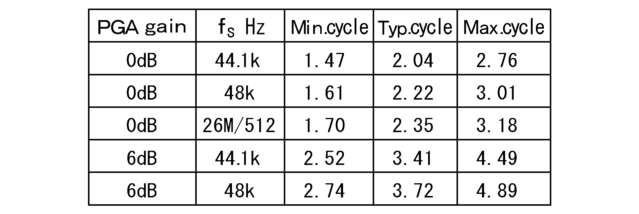
(利得と減衰量の制御タイミング差の設定について)
次に、可変利得アンプ12の利得制御のタイミングと、デジタル減衰器14の減衰量制御のタイミングとのタイミング差の設定について説明する。
次に、可変利得アンプ12の利得制御のタイミングと、デジタル減衰器14の減衰量制御のタイミングとのタイミング差の設定について説明する。
一例では、アナログ-デジタル変換器13を構成するΔΣ変調器の遅延、及び、可変利得アンプ12の遅延を合算すると、アナログ-デジタル変換器13の動作クロック周波数が128sの場合、約11サイクル又は12サイクルになる。 以下のように、ΔΣ変調器の遅延共通サイクル8を引き、別々に設定可能にしておく。
減衰量の設定が小→大のときに、ΔΣ変調器の遅延以外で3サイクル
減衰量の設定が大→小のときに、ΔΣ変調器の遅延以外で4サイクル
減衰量の設定が小→大のときに、ΔΣ変調器の遅延以外で3サイクル
減衰量の設定が大→小のときに、ΔΣ変調器の遅延以外で4サイクル
可変利得アンプ12の利得を設定してから、ΔΣ変調器の遅延8サイクルと、上記の可変利得アンプ12の遅延を合算したサイクルだけ遅延させた後、デジタル減衰器14の減衰量を設定する。実装の都合で、パイプラインを挿入する場合、パイプラインのサイクル数だけレジスタの設定推奨値を減らす。
(設定反映の遅延の実装について)
シフト・レジスタで遅延させる構成をとるものとすると、フリップフロップの数が100個と1kゲート規模になってしまう。ローパスフィルタの時定数で実現するものとすると、ゲートクロックが推論されず、HALT機能とHALT clock構成にしないと乗算・加算回路が常時動作し消費電力が無駄である。
シフト・レジスタで遅延させる構成をとるものとすると、フリップフロップの数が100個と1kゲート規模になってしまう。ローパスフィルタの時定数で実現するものとすると、ゲートクロックが推論されず、HALT機能とHALT clock構成にしないと乗算・加算回路が常時動作し消費電力が無駄である。
図8の外部入力が小→大の変化時には、即時に、可変利得アンプ12の利得及びデジタル減衰器14の減衰量を設定する必要があるため、仮に、エネルギー比較器16_1,16_2からの割り込みが2つ連続して入力される場合、利得設定及び減衰量設定の処理間隔を、それぞれの割り込みに対して別々に計測して各設定を実施する必要がある。
一方、外部入力が大→小の変化時には、0.025秒程度の差で可変利得アンプ12の利得及びデジタル減衰器14の減衰量を設定するため、動作クロック周波数が128fsであってもサイクル数に余裕がある。FSM(Finite State Machine:有限状態機械)の遷移間隔を、可変利得アンプ12の利得設定及びデジタル減衰器14の減衰量設定の処理間隔よりも遅くできる。
よって、実装・検証のしやすさと、消費電力の観点から、可変利得アンプ12の利得設定及びデジタル減衰器14の減衰量設定の処理間隔を管理するタイマーカウンタを3つ準備し、FSMで実装する。
可変利得アンプ12の利得設定の動作例のタイミング・ダイグラムを図9A及び図9Bに示す。図9A及び図9Bには、エネルギー比較器16_1(CMP_1)の出力信号、エネルギー比較器16_2(CMP_2)の出力信号、可変利得アンプ12の目標利得、及び、可変利得アンプ12の利得PVOLを示している。
可変利得アンプ12の利得設定及びデジタル減衰器14の減衰量設定の処理間隔を管理する3つのタイマーカウンタの動作例のタイミング・ダイグラムを図10A及び図10Bに示す。図10A及び図10Bには、CMP_1の出力信号、CMP_2の出力信号、可変利得アンプ12の目標利得、可変利得アンプ12の利得PVOL、及び、デジタル減衰器14の減衰量MVOLを示している。
可変利得アンプ12の利得PVOLを下げるタイミングは即時である。可変利得アンプ12の利得PVOLを上げていくタイミング間隔は常に一定になるように制御する。可変利得アンプ12の利得PVOLの設定、及び、デジタル減衰器14の減衰量MVOLの設定の遅延も、設定以外のタイミングにならないように、換言すれば、時間差が一定になるように制御する。
(レベル割り込みと可変利得アンプの利得設定について)
エネルギー比較器16_1(CMP_1)の出力信号、及び、エネルギー比較器16_2(CMP_2)の出力信号については、レベル割り込みとして扱う。2系統の割り込みは、512fsのクロックで非同期乗り換えした後、それぞれイネーブルレジスタによって割り込みを利用するか否かを決定する。両方有効の際には、優先付き割り込みとして、CMP_1を優先的に処理する。
エネルギー比較器16_1(CMP_1)の出力信号、及び、エネルギー比較器16_2(CMP_2)の出力信号については、レベル割り込みとして扱う。2系統の割り込みは、512fsのクロックで非同期乗り換えした後、それぞれイネーブルレジスタによって割り込みを利用するか否かを決定する。両方有効の際には、優先付き割り込みとして、CMP_1を優先的に処理する。
よって、CMP_1の閾値設定レジスタCMPnHx_VTHに電力を大きく設定し、割り込み要求を処理する際に設定する可変利得アンプ12の利得設定レジスタCMPx_VOLについては、CMP_1の方に小さな利得を設定する。アナログ入力系統nとエネルギー比較器の系統x毎に設定値のレジスタを準備する。
より優先度の高い割り込みが存在しない場合、割り込みの系統に対応した目標利得設定値に、可変利得アンプ12の利得PVOLを設定するように動作する。現在設定している可変利得アンプ12の利得PVOLと、割り込みに対応した目標利得設定値との大小関係で動作が異なる。
1.割り込みに対応した目標利得設定値よりも、現在の利得設定値が高い場合
即座に設定レジスタの値に可変利得アンプ12の利得を設定する。
2.割り込みに対応した目標利得設定値よりも、現在の利得設定値が低い場合
所定のレジスタに設定したインターバルで可変利得アンプ12の利得を目標値に漸近させていく。一度に遷移する可変利得アンプ12の利得ステップは通常0.2dBである。設定値は可変とする。
即座に設定レジスタの値に可変利得アンプ12の利得を設定する。
2.割り込みに対応した目標利得設定値よりも、現在の利得設定値が低い場合
所定のレジスタに設定したインターバルで可変利得アンプ12の利得を目標値に漸近させていく。一度に遷移する可変利得アンプ12の利得ステップは通常0.2dBである。設定値は可変とする。
可変利得アンプ12の利得は、レジスタ値を整数表現して0.2倍にした値を実際の値とする。可変利得アンプ12の利得設定の上限、下限を設定できるようにする。
利得設定の下限値は、外部マイクの最大入力がプリアンプ11を経由しても、アナログ-デジタル変換器13の入力レンジを使い切れない場合を想定して設定する。最大入力でも、+6dB利得ではなく、+3dB利得で使うことを可能とする。この値を最小利得pminとする。
利得設定の上限値は、利得が高いときの可変利得アンプ12の雑音指数が悪く、システム全体で、通常動作時のS/Nをかえって悪化させてしまう場合があることを想定している。+6dBで使うよりも+4dBで使う方がよいときに対応する。この値を最大利得pmaxとする。
プリアンプ11からのオーディオ信号の出力から、可変利得アンプ12の利得設定までの遅延時間の説明図を図11に示す。
エネルギー比較器16_1,16_2の遅延量の一例は0.4μsである。レベル割り込みは、システムで最速、かつ、制御部17の動作クロックと同期関係にある最速のクロックで非同期乗り換えする。最速が512fsの周波数で、fs=44.1kHzの場合0.089μsである。この割り込み信号を利用してFSMを動作し、制御レジスタ値を操作するので、最速でも制御部17の動作クロックの1サイクルの遅延が発生する。
非同期乗り換えと制御部17の動作による遅延により、制御部17のARC回路171_1、171_2の入力レベルの比較判定から、可変利得アンプ12の利得設定までの遅延は、これらの合算になる。制御部17の動作クロック128fsと源振の1/4の速度とすると、16_1,16_2の出力から512fsクロックの6サイクルから10サイクルの遅延が発生する。時間にすると、0.666μsから0.834μsのため、この部分の遅延は無視するシステムとする。
(減衰量の設定について)
デジタル減衰器14_1,14_2の減衰量の設定については、最小利得pmin、及び、可変利得アンプ12_1,12_2の利得設定値pvolの2つで決定する。利得設定値pvolは、図2の制御値N_p1,N_p2に相当する。ここで、減衰量をmattとし、負数のボリューム表現をmvolとすると、負数のボリューム表現mvolは、
mvol=pmin-pvol
となり、減衰量mattは、
matt=pvol-pmin
となる。最小利得pmin、利得設定値pvol、及び、最大利得pmaxの大小関係は、
pmin≦pvol≦pmax
である。
デジタル減衰器14_1,14_2の減衰量の設定については、最小利得pmin、及び、可変利得アンプ12_1,12_2の利得設定値pvolの2つで決定する。利得設定値pvolは、図2の制御値N_p1,N_p2に相当する。ここで、減衰量をmattとし、負数のボリューム表現をmvolとすると、負数のボリューム表現mvolは、
mvol=pmin-pvol
となり、減衰量mattは、
matt=pvol-pmin
となる。最小利得pmin、利得設定値pvol、及び、最大利得pmaxの大小関係は、
pmin≦pvol≦pmax
である。
表3は、デジタル減衰器14_1,14_2を制御するレジスタMIC_VOLの設定仕様の一例である。レジスタMIC_VOLは、図2の制御値生成部171_12,171_22内に設けられている。ミュート(Mute)及び0dB設定が変則である。可変利得アンプ12_1,12_2の利得設定値pvolを使った規則的な演算で、負数のボリューム表現mvolをデジタル減衰器14_1,14_2に出力する。8ビット目に見えない符号ビットを考え、それを削除してインターフェースしている、と考えると、2の補数で表現できる。ミュートを指定すると問題になるため、負数側は、0×82でオーバーフロー処理をする。正数側は、0×00で処理をする。
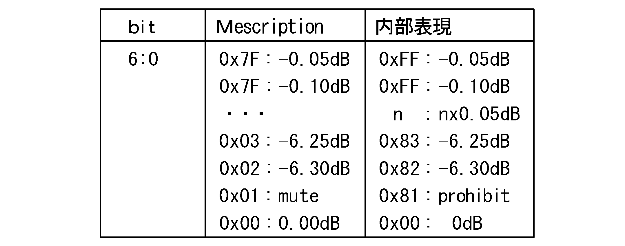
0.2や0.05をそのまま2進数の固定小数で表現すると無理数になるため、整数に変換して扱う。利得設定値pvolのステップの最小単位は0.2dBであり、負数のボリューム表現mvolのステップの4倍である。よって、pvol,pmin,pmaxをそれぞれ5倍した整数値PVOL,PMIN,PMAXを使って演算した結果を、更に4倍した値MVOLがデジタル減衰器14_1,14_2に供給される信号レベルになる。MVOLの最上位ビットである符号ビットを除いてインターフェースする。整数値PVOL,PMIN,PMAXは出力信号及びレジスタ設定値と同じある。
デジタル減衰器14_1,14_2は、チャンネル単位で 調整を取るために、減衰量を0.2dBよりも細かく設定可能である。デジタル減衰器14_1,14_2の減衰量は、固定量のため、独立してオフセットを与えることができる。
[実施形態に係る制御方法、及び、作用、効果]
上記の構成の本実施形態に係るアナログ-デジタル変換装置10は、入力されるアナログ信号のレベルを検出し、その検出レベルに基づいて、可変利得アンプ12の利得、及び、デジタル減衰器14の減衰量を制御するフィードフォワード制御の構成となっている。そして、フィードフォワード制御であることで、フィードバック制御に比べて、制御ループの応答性に優れたアナログ-デジタル変換装置を提供できる。
上記の構成の本実施形態に係るアナログ-デジタル変換装置10は、入力されるアナログ信号のレベルを検出し、その検出レベルに基づいて、可変利得アンプ12の利得、及び、デジタル減衰器14の減衰量を制御するフィードフォワード制御の構成となっている。そして、フィードフォワード制御であることで、フィードバック制御に比べて、制御ループの応答性に優れたアナログ-デジタル変換装置を提供できる。
更に、本実施形態に係るアナログ-デジタル変換装置10によれば、次のような作用、効果を得ることができる。
・オーディオ用途において、アナログ-デジタル変換器13(13_1,13_2)の入力ダイナミックレンジよりも広い動作時のダイナミックレンジを得ることができる。
・突発的な強入力変化に対して、オーディオで問題になるポップノイズの発生を十分に抑制することができる。
・信号強度が一定の可聴帯域信号の入力時は、入力信号にシステムからの影響を与えず一定の静特性を得ることができる。
・強入力から弱入力に変化したときに違和感なく、ダイナミックレンジの拡大を行うことができる。
・アナログ・ブロックは、比較器と論理和で構成するエネルギー比較器を追加し、細かい利得設定を可能にする必要があるが、回路規模が小規模な構成で実現できる。
・デジタル・ブロックは、DSP(Digital Signal Processor)等による演算が不要で、FSMを主体とした小規模な構成で実現することができる。
・オーディオ用途において、アナログ-デジタル変換器13(13_1,13_2)の入力ダイナミックレンジよりも広い動作時のダイナミックレンジを得ることができる。
・突発的な強入力変化に対して、オーディオで問題になるポップノイズの発生を十分に抑制することができる。
・信号強度が一定の可聴帯域信号の入力時は、入力信号にシステムからの影響を与えず一定の静特性を得ることができる。
・強入力から弱入力に変化したときに違和感なく、ダイナミックレンジの拡大を行うことができる。
・アナログ・ブロックは、比較器と論理和で構成するエネルギー比較器を追加し、細かい利得設定を可能にする必要があるが、回路規模が小規模な構成で実現できる。
・デジタル・ブロックは、DSP(Digital Signal Processor)等による演算が不要で、FSMを主体とした小規模な構成で実現することができる。
[実装例]
続いて、図2に示す本実施形態に係るアナログ-デジタル変換装置10の実装例について説明する。
続いて、図2に示す本実施形態に係るアナログ-デジタル変換装置10の実装例について説明する。
(512fs動作ブロックの実装例)
図12は、512fs動作ブロックの実装例について説明する図である。エネルギー比較器16_1,16_2の入力A_W_AINn_CMPxを単純な同期回路で同期してレベル割り込み信号AINn_CMPxとして出力する。割リ込みのアサートとネゲートに対応した応答処理に要求する時間に大きな差がある。アサート時は即座ですが、ネゲート時は最低でも、128fsのクロックで動作するFSMで32サイクル以上のインターバルでデータ遷移を促す。よって、レベル割り込み信号のチャタリング除去はFSMで制御すればよく、入力段は対応不要なため実施しない。これにより、割り込みアサート時も同期化した信号が最速でアサートする。
図12は、512fs動作ブロックの実装例について説明する図である。エネルギー比較器16_1,16_2の入力A_W_AINn_CMPxを単純な同期回路で同期してレベル割り込み信号AINn_CMPxとして出力する。割リ込みのアサートとネゲートに対応した応答処理に要求する時間に大きな差がある。アサート時は即座ですが、ネゲート時は最低でも、128fsのクロックで動作するFSMで32サイクル以上のインターバルでデータ遷移を促す。よって、レベル割り込み信号のチャタリング除去はFSMで制御すればよく、入力段は対応不要なため実施しない。これにより、割り込みアサート時も同期化した信号が最速でアサートする。
可変利得アンプ12_1,12_2の利得設定については、利得設定値A_W_PGAx_VOLを与えた後に設定信号A_W_PGAx_CHGをアサートして実現する。512fs動作ブロックでは、設定信号A_W_PGAx_CHGの生成に専用のFSMを構成する。128fsのクロックで動作しているFSMから生成される可変利得アンプ12_1,12_2の利得設定値を観測する。変化の検出を待機しているIDLE(1)ステート、変化を検出したら遷移するCHG(2)ステート、CHGステートから無条件に512fs1サイクルで遷移するHOLD(3)ステート、非同期リセット時に遷移するRESET(0)ステートで構成する。RESETステートからは非同期リセットが解除された後、無条件にIDLEステートに遷移する。このように構成し、ステート値を保持した2bitレジスタの最上位ビット側を、可変利得アンプ12_1,12_2の利得値を設定する信号として出力する。
(128fs動作ブロックの実装例1)
図13A及び図13Bは、128fs動作ブロックの実装例1について説明するタイミング・ダイグラムである。実装例1では、128fsクロックで動作するFSM、FSMで生成される制御信号で動作するブロックから利得設定値PVOL(A_W_PGAx_VOL)と減衰量設定信号MVOL(A_M_MICx_VOL)を生成する概要について説明する。
図13A及び図13Bは、128fs動作ブロックの実装例1について説明するタイミング・ダイグラムである。実装例1では、128fsクロックで動作するFSM、FSMで生成される制御信号で動作するブロックから利得設定値PVOL(A_W_PGAx_VOL)と減衰量設定信号MVOL(A_M_MICx_VOL)を生成する概要について説明する。
目標利得設定値がFSMの入力で利用する優先割り込み信号と割り込みに応じて設定されることも示している。目標利得設定値は、可変利得アンプ12_1,12_2の利得PVOLの生成に利用される。利得PVOLは、FSM内部で管理されて設定すべき値を出力する。
回路規模を小さく実現するために、利得設定タイミングと減衰量設定タイミングの遅延制御は3つの遅延タイマーによって構成する。いずれの遅延タイマーも、スタート信号で動作を開始し、あらかじめ決められた設定閾値に到達したら、減衰量設定信号を利得設定値から生成する。3つの遅延タイマーは、エネルギー比較器CMP1がアサートしたら動作を開始する遅延タイマー1、エネルギー比較器CMP2のみがアサートしたら動作を開始する遅延タイマー2、エネルギー比較器CMP1,CMP2のアサート状態で決定される目標利得設定値が現在の利得設定値よりも低く設定されるタイミングで動作を開始する遅延タイマー3で構成される。
エネルギー比較器CMP1,CMP2がアサートしたときに設定される利得設定値は一定である。レジスタによって可変とする。図中では、遅延タイマー1で参照されるエネルギー比較器CMP1がアサートしたときに設定される目標利得設定値PVOL1は、最小利得pminである。AINx_CMP1_VOLレジスタに設定値を格納し、信号名CSYN_AINxCMP1_VOLとして供給される。
遅延タイマー2で参照されるエネルギー比較器CMP2がアサートしたときに設定される目標利得設定値PVOL2は、中間利得であり、AINx_CMP2_VOLレジスタに設定値を格納し、CSYN_AINxCMP2_VOLとして供給される。遅延タイマー3で参照される目標利得設定値は現在設定している利得値PVOLとなる。
3つの遅延タイマーの終了タイミング、及び、供給される利得設定値から、減衰量設定値MVOLが、信号名A_M_MICx_VOLとして生成される。減衰量設定値MVOLが、デジタルメーションフィルタ15の入力信号の振幅を決定する。
(128fs動作ブロックの実装例2)
図14は、128fs動作ブロックの実装例2について説明する図である。実装例2は、利得設定値PVOL(A_W_PGAx_VOL)を固定値に強制設定する実装例である。通常は、FSMにより設定値が制御されるが、固定設定レジスタPGAx_VOL、信号名CSYN_PGAx_VOLの値をイネーブルがアサートしたときに反映される。
図14は、128fs動作ブロックの実装例2について説明する図である。実装例2は、利得設定値PVOL(A_W_PGAx_VOL)を固定値に強制設定する実装例である。通常は、FSMにより設定値が制御されるが、固定設定レジスタPGAx_VOL、信号名CSYN_PGAx_VOLの値をイネーブルがアサートしたときに反映される。
(128fs動作ブロックの実装例3)
図15Aは、128fs動作ブロックの実装例3についての説明図であり、図15Bは、実装例3についての説明に供するタイミング・ダイグラムである。実装例3は、FSMの実装例である。
図15Aは、128fs動作ブロックの実装例3についての説明図であり、図15Bは、実装例3についての説明に供するタイミング・ダイグラムである。実装例3は、FSMの実装例である。
FSMを制御するカウンタが1つある。0以外の値のときにインクリメントする実装である。このカウンタは、目標利得設定値が現在の利得設定値PVOLよりも大きいときに一定間隔で可変利得アンプ12_1,12_2の利得を変化させるFSM動作を制御するものである。
FSMは、CSYN_ARCx_EN信号がアサートしているときに動作する。ネゲートしているときはRESET(0)ステートにいる。CSYN_ARCx_EN信号がアサートすると、RESET(0)ステートからEQUAL(1)ステートに遷移する。
EQUAL(1)ステートでは、利得設定値PVOLが目標利得設定値と等しいときにEQUAL(1)ステートに留まる。割り込みにより 目標利得設定値が更新され、その値が現在の利得設定値より高いとき、一定タイミング毎に可変利得アンプ12_1,12_2の利得を設定値レジスタARCxPGA_STEP、信号名CSYN_ARCxPGA_STEP、通常時、0.2dBステップ相当上昇するためのステートに遷移する。
LESS_THAN(2)ステートに遷移し、同時に、FSM制御カウンタを1にセットしてインクリメントを開始する。FSM制御カウンタが32に到達したらINTERVAL(3)ステートに遷移する。INTERVAL(3)ステートでは、利得設定値をARCxPGA_STEPレジスタに設定された単位、通常0.2dB相当でステップアップしていく時間間隔を、FSM制御カウンタを観測して作り出す。
可聴帯域外の低い周波数の1周期に相当するため、FSMの動作クロック128fsで動作するカウンタの下位ビットは無視して上位ビットだけの比較でタイミングを作り出せる。カウンタの上位ビットと比較するための閾値はARCnTIMER_THレジスタ、信号名CSYN_ARCnTIMER_THで行う。カウンタが閾値に逹したら、LESS_THAN(2)ステートに遷移し、FSM制御カウンタを1に設定し直して次のインターバルを作り出す。
INTERVAL(3)ステートからLESS_THAN(2)ステートへの遷移時に利得設定値PVOLをステップアップした値に更新する。同時に、減衰量設定値MVOLを、遅延差を持って動作させるための遅延タイマー3のインクリメント動作を開始し、更新値を、減衰量設定値MVOLを生成する回路に通達するためのPVOL3レジスタを利得設定値PVOLと同じ値に設定する。遷移時に遅延タイマー3を動作開始させるため、遷移判定したサイクルでのみアサートするスタート3信号を生成する。
割り込みによって更新される目標利得設定値が、現在の利得設定値よりも低いとき、どのステートであっても、次のサイクルで可変利得アンプ12_1,12_2の利得を目標値に設定してEQUAL(1)ステートに遷移する。同時に発生した割り込みに応じてデジタル減衰器14_1,14_2の制御用の遅延タイマー1もしくは遅延タイマー2のインクリメント動作を開始する。遅延タイマー1/遅延タイマー2のインクリメント動作開始にはスタート信号を生成する。
この論理は、現在の利得設定値が目標利得設定値よりも大きい、で実現できる。次のサイクルでは必ず現在の利得設定値は目標利得設定値と等しくなるためである。FSM制御用のカウンタも0に設定して動作を停止させる。
いずれの遅延タイマーも、0以外の値でインクリメント、スタート信号がアサートしたら次のサイクルに1に設定、閾値に到達したら0に設定される論理で構成する。
(128fs動作ブロックの実装例4)
実装例4は、遅延タイマーの動作例である。遅延タイマーの動作のタイミング・ダイアグラムの一例を図16に示す。ここでは、遅延タイマーの閾値が、31を越えることはない前提で規定している。
実装例4は、遅延タイマーの動作例である。遅延タイマーの動作のタイミング・ダイアグラムの一例を図16に示す。ここでは、遅延タイマーの閾値が、31を越えることはない前提で規定している。
図16のタイミング・ダイアグラムは、遅延タイマーの閾値が最大設定値31のときを表している。遅延タイマーの閾値は、先述した(利得と減衰量の制御タイミング差の設定について)の項で規定した通りに準備する128fsΔΣ変調器で最大12サイクル、同じトポロジーのΔΣ変調器を64fsで動作させた場合でもΔΣ変調器による遅延サイクルが16のため、最大でも20サイクルである。従って、遅延タイマーの閾値については、31の設定で十分である。
遅延タイマーは、2つの利得設定値を低い方へ遷移させるために発生するFSMとは異なるタイミングのイベントと利得設定値を高い方へ遷移させる1つのFSMによるイベントによる、異なる3つの利得設定の変化点から、小規模な回路動作でデジタル減衰器14_1,14_2の変化点を作るための回路である。
それぞれ独立してタイミングが発生するため、いずれかの遅延タイマーが閾値に到達したときのタイミングで、それぞれのイベントに適した減衰量設定値を生成する。減衰量設定値は、利得設定値から計算されるもののため、現在の利得設定値とは別に、タイミング毎に適切な利得設定値PVOL1,PVOL2,PVOL3を参照する。それぞれ独立したタイミングで発生し、先述した(可変利得アンプの利得設定動作の遅延について)の項にて、遅延時間の定義を利得別ではなく、利得設定の変化方向で遅延サイクルを定義することを規定している。これは遅延タイマー1と 遅延タイマー2との遅延サイクル数を同じにして、閾値到達までの時間が絶対に前後しないことを保証する。
設定遅延が128fs単位のため誤差の知覚は無視でき、実装を軽くする前提のためにかけた制限である。遅延タイマー3が動作中に、エネルギー比較器16_1,16_2からの割り込みで発生する利得設定値変更は発生し得るため、遅延タイマー3の停止のための条件は、遅延タイマー1もしくは遅延タイマー2が閾値に到達したタイミングを含む。よって、遅延タイマー3の閾値到達が遅延タイマー1もしくは遅延タイマー2の閾値到達と同時の場合は、遅延タイマー1もしくは遅延タイマー2の閾値到達が優先されるため、可変利得アンプ12_1,12_2の利得変更の即時有効の動作を、デジタル減衰器14_1,14_2の制御でも優先的に実行できる。
このように、遅延タイマーの動作によって、デジタル減衰器14_1,14_2に設定する減衰量設定値の設定タイミングの優先順位も確定するので、減衰量設定値を保持するレジスタは、それぞれの遅延タイマーの到達タイミング時に遅延タイマーに応じた利得設定値PVOL1,PVOL2,PVOL3の値を参照して値を確定する回路を、優先順位を考慮せずに構成できる。
減衰量設定値MVOLの生成については、先述した(減衰量の設定について)の項で定義した算出式で決定し、オーバーフロー処理も施す。遅延タイマーの閾値到達タイミングを1サイクル早く通達して減衰量設定値MVOLの生成のための利得設定値PVOL1,PVOL2,PVOL3の値の選択を1サイクル早く確定し、パイプラインで保持す。そのため、先述した(利得と減衰量の制御タイミング差の設定について)の項で定義したように、遅延タイマーの閾値を制御する設定レジスタには1サイクル小さい値を与える。
<本開示の実施形態に係るオーディオ装置>
以上説明した本開示の実施形態に係るアナログ-デジタル変換装置10は、アナログ-デジタル変換装置を備える各種のオーディオ装置において、当該アナログ-デジタル変換装置として用いることができる。
以上説明した本開示の実施形態に係るアナログ-デジタル変換装置10は、アナログ-デジタル変換装置を備える各種のオーディオ装置において、当該アナログ-デジタル変換装置として用いることができる。
図17は、本開示の実施形態に係るアナログ-デジタル変換装置10を用いる、本開示の実施形態に係るオーディオ装置のシステム構成の概略を示すブロック図である。本実施形態に係るオーディオ装置100は、例えば、マイクロホン110、アナログ-デジタル変換装置120、信号処理部130、デジタル-アナログ変換装置140、及び、スピーカ150を備える構成となっている。
上記の構成のオーディオ装置100において、マイクロホン110から入力されるアナログのオーディオ信号をオーディオPCM信号に変換するアナログ-デジタル変換装置120として、先述した実施形態に係るアナログ-デジタル変換装置10を用いることができる。このアナログ-デジタル変換装置10は、入力されるアナログのオーディオ信号のレベルを検出し、その検出レベルに基づいて利得制御を行うフィードフォワード制御であることから、アナログ-デジタル変換装置120として、制御ループの応答性に優れたアナログ-デジタル変換装置を実現できる。
<変形例>
以上、本開示の技術について、好ましい実施形態に基づき説明したが、本開示の技術は当該実施形態に限定されるものではない。上記の実施形態において説明したアナログ-デジタル変換装置及びオーディオ装置の構成、構造は例示であり、適宜、変更することができる。
以上、本開示の技術について、好ましい実施形態に基づき説明したが、本開示の技術は当該実施形態に限定されるものではない。上記の実施形態において説明したアナログ-デジタル変換装置及びオーディオ装置の構成、構造は例示であり、適宜、変更することができる。
例えば、上記の実施形態では、アナログ-デジタル変換装置10をオーディオ装置100に適用する場合を例に挙げて説明したが、オーディオ装置への適用に限られるものではない。また、上記の実施形態では、アナログ-デジタル変換装置10におけるアナログ-デジタル変換器13として、ΔΣ変調器から成るアナログ-デジタル変換器(デルタ-シグマ変調型アナログ-デジタル変換器)を用いるものとしたが、これに限られるものではなく、逐次比較型アナログ-デジタル変換器など、他の形態のアナログ-デジタル変換器を用いることができる。
<本開示がとることができる構成>
尚、本開示は、以下のような構成をとることもできる。
尚、本開示は、以下のような構成をとることもできる。
≪A.アナログ-デジタル変換装置≫
[A-1]入力されるアナログ信号を増幅する可変利得アンプ、
可変利得アンプを経たアナログ信号をデジタル信号に変換するアナログ-デジタル変換器、
アナログ-デジタル変換器から出力されるデジタル信号を減衰させる減衰器、
アナログ信号のレベルを検出するレベル検出部、及び、
レベル検出部の検出レベルに基づいて、可変利得アンプの利得、及び、減衰器の減衰量を制御する制御部を備える、
アナログ-デジタル変換装置。
[A-2]入力されるアナログ信号を取り込んで可変利得アンプに供給するプリアンプを有し、
レベル検出部は、プリアンプを経た後のアナログ信号のレベルを検出する、
上記[A-1]に記載のアナログ-デジタル変換装置。
[A-3]レベル検出部は、互いに異なる閾値を有する複数の比較器を有する、
上記[A-2]に記載のアナログ-デジタル変換装置。
[A-4]レベル検出部は、プリアンプの出力信号のバイアスよりも高い第1の閾値を有する第1の比較器、及び、プリアンプの出力信号のバイアスよりも低い第2の閾値を有する第2の比較器を有する、
上記[A-3]に記載のアナログ-デジタル変換装置。
[A-5]第1の比較器は、アナログ信号のレベルが第1の閾値よりも高いときに真の論理を出力し、
第2の比較器は、アナログ信号のレベルが第2の閾値よりも低いときに真の論理を出力する、
上記[A-4]に記載のアナログ-デジタル変換装置。
[A-6]レベル検出部は、第1の比較器の出力、及び、第2の比較器の出力の論理和を、アナログ信号の検出レベルとして出力する、
上記[A-5]に記載のアナログ-デジタル変換装置。
[A-7]プリアンプは、可変利得アンプ及びレベル検出器の動作変化に対して、出力インピーダンスを一定にする役割を持っている、
上記[A-1]乃至上記[A-6]のいずれかに記載のアナログ-デジタル変換装置。
[A-8]制御部は、減衰器の減衰量を、可変利得アンプの利得を相殺する値に制御する、
上記[A-1]乃至上記[A-7]のいずれかに記載のアナログ-デジタル変換装置。
[A-9]制御部は、減衰器の減衰量を、可変利得アンプの制御タイミングに対して一定のタイミング差を維持しながら制御する、
[A-8]に記載のアナログ-デジタル変換装置。
[A-10]アナログ-デジタル変換器は、可変利得アンプを経たアナログ信号をオーバーサンプリングし、アナログ信号の振幅に応じたパルス列の信号に変換するデルタ-シグマ変調器から成る、
上記[A-1]乃至上記[A-9]のいずれかに記載のアナログ-デジタル変換装置。
[A-11]デルタ-シグマ変調器から出力され、減衰器を経たパルス列の信号を、折り返し雑音の影響を受けずに必要な信号情報を取得できるサンプリング周波数のデジタル信号に変換するデシメーションフィルタを有する、
上記[A-10]に記載のアナログ-デジタル変換装置。
[A-1]入力されるアナログ信号を増幅する可変利得アンプ、
可変利得アンプを経たアナログ信号をデジタル信号に変換するアナログ-デジタル変換器、
アナログ-デジタル変換器から出力されるデジタル信号を減衰させる減衰器、
アナログ信号のレベルを検出するレベル検出部、及び、
レベル検出部の検出レベルに基づいて、可変利得アンプの利得、及び、減衰器の減衰量を制御する制御部を備える、
アナログ-デジタル変換装置。
[A-2]入力されるアナログ信号を取り込んで可変利得アンプに供給するプリアンプを有し、
レベル検出部は、プリアンプを経た後のアナログ信号のレベルを検出する、
上記[A-1]に記載のアナログ-デジタル変換装置。
[A-3]レベル検出部は、互いに異なる閾値を有する複数の比較器を有する、
上記[A-2]に記載のアナログ-デジタル変換装置。
[A-4]レベル検出部は、プリアンプの出力信号のバイアスよりも高い第1の閾値を有する第1の比較器、及び、プリアンプの出力信号のバイアスよりも低い第2の閾値を有する第2の比較器を有する、
上記[A-3]に記載のアナログ-デジタル変換装置。
[A-5]第1の比較器は、アナログ信号のレベルが第1の閾値よりも高いときに真の論理を出力し、
第2の比較器は、アナログ信号のレベルが第2の閾値よりも低いときに真の論理を出力する、
上記[A-4]に記載のアナログ-デジタル変換装置。
[A-6]レベル検出部は、第1の比較器の出力、及び、第2の比較器の出力の論理和を、アナログ信号の検出レベルとして出力する、
上記[A-5]に記載のアナログ-デジタル変換装置。
[A-7]プリアンプは、可変利得アンプ及びレベル検出器の動作変化に対して、出力インピーダンスを一定にする役割を持っている、
上記[A-1]乃至上記[A-6]のいずれかに記載のアナログ-デジタル変換装置。
[A-8]制御部は、減衰器の減衰量を、可変利得アンプの利得を相殺する値に制御する、
上記[A-1]乃至上記[A-7]のいずれかに記載のアナログ-デジタル変換装置。
[A-9]制御部は、減衰器の減衰量を、可変利得アンプの制御タイミングに対して一定のタイミング差を維持しながら制御する、
[A-8]に記載のアナログ-デジタル変換装置。
[A-10]アナログ-デジタル変換器は、可変利得アンプを経たアナログ信号をオーバーサンプリングし、アナログ信号の振幅に応じたパルス列の信号に変換するデルタ-シグマ変調器から成る、
上記[A-1]乃至上記[A-9]のいずれかに記載のアナログ-デジタル変換装置。
[A-11]デルタ-シグマ変調器から出力され、減衰器を経たパルス列の信号を、折り返し雑音の影響を受けずに必要な信号情報を取得できるサンプリング周波数のデジタル信号に変換するデシメーションフィルタを有する、
上記[A-10]に記載のアナログ-デジタル変換装置。
≪B.アナログ-デジタル変換装置の制御方法≫
[B-1]入力されるアナログ信号を増幅する可変利得アンプ、
可変利得アンプを経たアナログ信号をデジタル信号に変換するアナログ-デジタル変換器、及び、
アナログ-デジタル変換器から出力されるデジタル信号を減衰させる減衰器を備えるアナログ-デジタル変換装置の制御に当たって、
アナログ信号のレベルを検出し、
その検出レベルに基づいて、可変利得アンプの利得、及び、減衰器の減衰量の制御を行う、
アナログ-デジタル変換装置の制御方法。
[B-2]デルタ-シグマ変調器から出力され、減衰器を経たパルス列の信号を、折り返し雑音の影響を受けずに必要な信号情報を取得できるサンプリング周波数のデジタル信号に変換する、
上記[B-1]に記載のアナログ-デジタル変換装置の制御方法。
[B-1]入力されるアナログ信号を増幅する可変利得アンプ、
可変利得アンプを経たアナログ信号をデジタル信号に変換するアナログ-デジタル変換器、及び、
アナログ-デジタル変換器から出力されるデジタル信号を減衰させる減衰器を備えるアナログ-デジタル変換装置の制御に当たって、
アナログ信号のレベルを検出し、
その検出レベルに基づいて、可変利得アンプの利得、及び、減衰器の減衰量の制御を行う、
アナログ-デジタル変換装置の制御方法。
[B-2]デルタ-シグマ変調器から出力され、減衰器を経たパルス列の信号を、折り返し雑音の影響を受けずに必要な信号情報を取得できるサンプリング周波数のデジタル信号に変換する、
上記[B-1]に記載のアナログ-デジタル変換装置の制御方法。
≪C.オーディオ装置≫
[C-1]入力されるアナログ信号を増幅する可変利得アンプ、
可変利得アンプを経たアナログ信号をデジタル信号に変換するアナログ-デジタル変換器、
アナログ-デジタル変換器から出力されるデジタル信号を減衰させる減衰器、
アナログ信号のレベルを検出するレベル検出部、及び、
レベル検出部の検出レベルに基づいて、可変利得アンプの利得、及び、減衰器の減衰量を制御する制御部を備える、
アナログ-デジタル変換装置を有するオーディオ装置。
[C-2]入力されるアナログ信号を取り込んで可変利得アンプに供給するプリアンプを有し、
レベル検出部は、プリアンプを経た後のアナログ信号のレベルを検出する、
上記[C-1]に記載のオーディオ装置。
[C-3]レベル検出部は、互いに異なる閾値を有する複数の比較器を有する、
上記[C-2]に記載のオーディオ装置。
[C-4]レベル検出部は、プリアンプの出力信号のバイアスよりも高い第1の閾値を有する第1の比較器、及び、プリアンプの出力信号のバイアスよりも低い第2の閾値を有する第2の比較器を有する、
上記[C-3]に記載のオーディオ装置。
[C-5]第1の比較器は、アナログ信号のレベルが第1の閾値よりも高いときに真の論理を出力し、
第2の比較器は、アナログ信号のレベルが第2の閾値よりも低いときに真の論理を出力する、
上記[C-4]に記載のオーディオ装置。
[C-6]レベル検出部は、第1の比較器の出力、及び、第2の比較器の出力の論理和を、アナログ信号の検出レベルとして出力する、
上記[C-5]に記載のオーディオ装置。
[C-7]プリアンプは、可変利得アンプ及びレベル検出器の動作変化に対して、出力インピーダンスを一定にする役割を持っている、
上記[C-1]乃至上記[C-6]のいずれかに記載のオーディオ装置。
[C-8]制御部は、減衰器の減衰量を、可変利得アンプの利得を相殺する値に制御する、
上記[C-1]乃至上記[C-7]のいずれかに記載のオーディオ装置。
[C-9]制御部は、減衰器の減衰量を、可変利得アンプの制御タイミングに対して一定のタイミング差を維持しながら制御する、
[C-8]に記載のオーディオ装置。
[C-10]アナログ-デジタル変換器は、可変利得アンプを経たアナログ信号をオーバーサンプリングし、アナログ信号の振幅に応じたパルス列の信号に変換するデルタ-シグマ変調器から成る、
上記[C-1]乃至上記[C-9]のいずれかに記載のオーディオ装置。
[C-11]デルタ-シグマ変調器から出力され、減衰器を経たパルス列の信号を、折り返し雑音の影響を受けずに必要な信号情報を取得できるサンプリング周波数のデジタル信号に変換するデシメーションフィルタを有する、
上記[C-10]に記載のオーディオ装置。
[C-1]入力されるアナログ信号を増幅する可変利得アンプ、
可変利得アンプを経たアナログ信号をデジタル信号に変換するアナログ-デジタル変換器、
アナログ-デジタル変換器から出力されるデジタル信号を減衰させる減衰器、
アナログ信号のレベルを検出するレベル検出部、及び、
レベル検出部の検出レベルに基づいて、可変利得アンプの利得、及び、減衰器の減衰量を制御する制御部を備える、
アナログ-デジタル変換装置を有するオーディオ装置。
[C-2]入力されるアナログ信号を取り込んで可変利得アンプに供給するプリアンプを有し、
レベル検出部は、プリアンプを経た後のアナログ信号のレベルを検出する、
上記[C-1]に記載のオーディオ装置。
[C-3]レベル検出部は、互いに異なる閾値を有する複数の比較器を有する、
上記[C-2]に記載のオーディオ装置。
[C-4]レベル検出部は、プリアンプの出力信号のバイアスよりも高い第1の閾値を有する第1の比較器、及び、プリアンプの出力信号のバイアスよりも低い第2の閾値を有する第2の比較器を有する、
上記[C-3]に記載のオーディオ装置。
[C-5]第1の比較器は、アナログ信号のレベルが第1の閾値よりも高いときに真の論理を出力し、
第2の比較器は、アナログ信号のレベルが第2の閾値よりも低いときに真の論理を出力する、
上記[C-4]に記載のオーディオ装置。
[C-6]レベル検出部は、第1の比較器の出力、及び、第2の比較器の出力の論理和を、アナログ信号の検出レベルとして出力する、
上記[C-5]に記載のオーディオ装置。
[C-7]プリアンプは、可変利得アンプ及びレベル検出器の動作変化に対して、出力インピーダンスを一定にする役割を持っている、
上記[C-1]乃至上記[C-6]のいずれかに記載のオーディオ装置。
[C-8]制御部は、減衰器の減衰量を、可変利得アンプの利得を相殺する値に制御する、
上記[C-1]乃至上記[C-7]のいずれかに記載のオーディオ装置。
[C-9]制御部は、減衰器の減衰量を、可変利得アンプの制御タイミングに対して一定のタイミング差を維持しながら制御する、
[C-8]に記載のオーディオ装置。
[C-10]アナログ-デジタル変換器は、可変利得アンプを経たアナログ信号をオーバーサンプリングし、アナログ信号の振幅に応じたパルス列の信号に変換するデルタ-シグマ変調器から成る、
上記[C-1]乃至上記[C-9]のいずれかに記載のオーディオ装置。
[C-11]デルタ-シグマ変調器から出力され、減衰器を経たパルス列の信号を、折り返し雑音の影響を受けずに必要な信号情報を取得できるサンプリング周波数のデジタル信号に変換するデシメーションフィルタを有する、
上記[C-10]に記載のオーディオ装置。
10・・・アナログ-デジタル変換装置、11(11_1、11_2)・・・プリアンプ、12(12_1、12_2)・・・可変利得アンプ、13(13_1、13_2)・・・アナログ-デジタル変換器(ADC)、14(14_1、14_2)・・・デジタル減衰器、15・・・デシメーションフィルタ、16・・・レベル検出部、16_1(16_11、16_12)、16_2(16_21、16_22)・・・エネルギー比較器、17・・・制御部
Claims (13)
- 入力されるアナログ信号を増幅する可変利得アンプ、
可変利得アンプを経たアナログ信号をデジタル信号に変換するアナログ-デジタル変換器、
アナログ-デジタル変換器から出力されるデジタル信号を減衰させる減衰器、
入力されるアナログ信号のレベルを検出するレベル検出部、及び、
レベル検出部の検出レベルに基づいて、可変利得アンプの利得、及び、減衰器の減衰量を制御する制御部を備える、
アナログ-デジタル変換装置。 - 入力されるアナログ信号を取り込んで可変利得アンプに供給するプリアンプを有し、
レベル検出部は、プリアンプを経た後のアナログ信号のレベルを検出する、
請求項1に記載のアナログ-デジタル変換装置。 - レベル検出部は、互いに異なる閾値を有する複数の比較器を有する、
請求項2に記載のアナログ-デジタル変換装置。 - レベル検出部は、プリアンプの出力信号のバイアスよりも高い第1の閾値を有する第1の比較器、及び、プリアンプの出力信号のバイアスよりも低い第2の閾値を有する第2の比較器を有する、
請求項3に記載のアナログ-デジタル変換装置。 - 第1の比較器は、アナログ信号のレベルが第1の閾値よりも高いときに真の論理を出力し、
第2の比較器は、アナログ信号のレベルが第2の閾値よりも低いときに真の論理を出力する、
請求項4に記載のアナログ-デジタル変換装置。 - レベル検出部は、第1の比較器の出力、及び、第2の比較器の出力の論理和を、アナログ信号の検出レベルとして出力する、
請求項5に記載のアナログ-デジタル変換装置。 - プリアンプは、可変利得アンプ及びレベル検出器の動作変化に対して、出力インピーダンスを一定にする役割を持っている、
請求項1に記載のアナログ-デジタル変換装置。 - 制御部は、減衰器の減衰量を、可変利得アンプの利得を相殺する値に制御する、
請求項1に記載のアナログ-デジタル変換装置。 - 制御部は、減衰器の減衰量を、可変利得アンプの制御タイミングに対して一定のタイミング差を維持しながら制御する、
請求項8に記載のアナログ-デジタル変換装置。 - アナログ-デジタル変換器は、可変利得アンプを経たアナログ信号をオーバーサンプリングし、アナログ信号の振幅に応じたパルス列の信号に変換するデルタ-シグマ変調器から成る、
請求項1に記載のアナログ-デジタル変換装置。 - デルタ-シグマ変調器から出力され、減衰器を経たパルス列の信号を、折り返し雑音の影響を受けずに必要な信号情報を取得できるサンプリング周波数のデジタル信号に変換するデシメーションフィルタを有する、
請求項10に記載のアナログ-デジタル変換装置。 - 入力されるアナログ信号を増幅する可変利得アンプ、
可変利得アンプを経たアナログ信号をデジタル信号に変換するアナログ-デジタル変換器、及び、
アナログ-デジタル変換器から出力されるデジタル信号を減衰させる減衰器を備えるアナログ-デジタル変換装置の制御に当たって、
入力されるアナログ信号のレベルを検出し、
その検出レベルに基づいて、可変利得アンプの利得、及び、減衰器の減衰量の制御を行う、
アナログ-デジタル変換装置の制御方法。 - 入力されるアナログ信号を増幅する可変利得アンプ、
可変利得アンプを経たアナログ信号をデジタル信号に変換するアナログ-デジタル変換器、
アナログ-デジタル変換器から出力されるデジタル信号を減衰させる減衰器、
入力されるアナログ信号のレベルを検出するレベル検出部、及び、
レベル検出部の検出レベルに基づいて、可変利得アンプの利得、及び、減衰器の減衰量を制御する制御部を備える、
アナログ-デジタル変換装置を有するオーディオ装置。
Priority Applications (1)
| Application Number | Priority Date | Filing Date | Title |
|---|---|---|---|
| JP2021522694A JP7525484B2 (ja) | 2019-05-29 | 2020-04-15 | アナログ-デジタル変換装置、アナログ-デジタル変換装置の制御方法、及び、オーディオ装置 |
Applications Claiming Priority (2)
| Application Number | Priority Date | Filing Date | Title |
|---|---|---|---|
| JP2019-099965 | 2019-05-29 | ||
| JP2019099965 | 2019-05-29 |
Publications (1)
| Publication Number | Publication Date |
|---|---|
| WO2020241102A1 true WO2020241102A1 (ja) | 2020-12-03 |
Family
ID=73554024
Family Applications (1)
| Application Number | Title | Priority Date | Filing Date |
|---|---|---|---|
| PCT/JP2020/016629 Ceased WO2020241102A1 (ja) | 2019-05-29 | 2020-04-15 | アナログ-デジタル変換装置、アナログ-デジタル変換装置の制御方法、及び、オーディオ装置 |
Country Status (2)
| Country | Link |
|---|---|
| JP (1) | JP7525484B2 (ja) |
| WO (1) | WO2020241102A1 (ja) |
Cited By (1)
| Publication number | Priority date | Publication date | Assignee | Title |
|---|---|---|---|---|
| JPWO2022202772A1 (ja) * | 2021-03-24 | 2022-09-29 |
Citations (4)
| Publication number | Priority date | Publication date | Assignee | Title |
|---|---|---|---|---|
| JPH07146314A (ja) * | 1993-06-28 | 1995-06-06 | Csem Centre Suisse Electron & De Microtech Sa Rech & Dev | 可変利得入力ステージを備える信号処理回路 |
| US6288664B1 (en) * | 1999-10-22 | 2001-09-11 | Eric J. Swanson | Autoranging analog to digital conversion circuitry |
| JP2006165912A (ja) * | 2004-12-06 | 2006-06-22 | Rohm Co Ltd | 信号処理装置およびそれを用いた撮像装置 |
| JP2011155386A (ja) * | 2010-01-26 | 2011-08-11 | Seiko Epson Corp | 増幅回路、集積回路装置及び電子機器 |
-
2020
- 2020-04-15 JP JP2021522694A patent/JP7525484B2/ja active Active
- 2020-04-15 WO PCT/JP2020/016629 patent/WO2020241102A1/ja not_active Ceased
Patent Citations (4)
| Publication number | Priority date | Publication date | Assignee | Title |
|---|---|---|---|---|
| JPH07146314A (ja) * | 1993-06-28 | 1995-06-06 | Csem Centre Suisse Electron & De Microtech Sa Rech & Dev | 可変利得入力ステージを備える信号処理回路 |
| US6288664B1 (en) * | 1999-10-22 | 2001-09-11 | Eric J. Swanson | Autoranging analog to digital conversion circuitry |
| JP2006165912A (ja) * | 2004-12-06 | 2006-06-22 | Rohm Co Ltd | 信号処理装置およびそれを用いた撮像装置 |
| JP2011155386A (ja) * | 2010-01-26 | 2011-08-11 | Seiko Epson Corp | 増幅回路、集積回路装置及び電子機器 |
Cited By (4)
| Publication number | Priority date | Publication date | Assignee | Title |
|---|---|---|---|---|
| JPWO2022202772A1 (ja) * | 2021-03-24 | 2022-09-29 | ||
| WO2022202772A1 (ja) * | 2021-03-24 | 2022-09-29 | ヌヴォトンテクノロジージャパン株式会社 | アナログデジタル変換回路 |
| US20240007128A1 (en) * | 2021-03-24 | 2024-01-04 | Nuvoton Technology Corporation Japan | Analog-to-digital conversion circuit |
| JP7774614B2 (ja) | 2021-03-24 | 2025-11-21 | ヌヴォトンテクノロジージャパン株式会社 | アナログデジタル変換回路 |
Also Published As
| Publication number | Publication date |
|---|---|
| JP7525484B2 (ja) | 2024-07-30 |
| JPWO2020241102A1 (ja) | 2020-12-03 |
Similar Documents
| Publication | Publication Date | Title |
|---|---|---|
| CN101803202A (zh) | 基于超采样数字处理的低延迟信号处理 | |
| US9762255B1 (en) | Reconfiguring paths in a multiple path analog-to-digital converter | |
| US9031251B2 (en) | Digital noise-cancellation | |
| US9543975B1 (en) | Multi-path analog front end and analog-to-digital converter for a signal processing system with low-pass filter between paths | |
| US9407236B2 (en) | System and method for processing a signal with a filter employing FIR and IIR elements | |
| US9407224B2 (en) | Digital microphone device with extended dynamic range | |
| EP1753130B1 (en) | Analog-to-digital converter with dynamic range extension | |
| US9048861B2 (en) | Analogue to digital converter | |
| GB2553864A (en) | Matching paths in a multiple path analog-to-digital converter | |
| WO2020241102A1 (ja) | アナログ-デジタル変換装置、アナログ-デジタル変換装置の制御方法、及び、オーディオ装置 | |
| US7345606B2 (en) | DA-converter system and a method for converting a multi-bit digital signal to an analog signal | |
| JP2000049613A (ja) | ディジタルスイッチングアンプ | |
| JP2001251190A (ja) | デルタシグマd/a変換器 | |
| JP2020190642A (ja) | Ancシステム | |
| JP2015519020A (ja) | 可変の供給電圧のためのスイッチング増幅器 | |
| CN117202018A (zh) | 音量控制电路、音量控制方法、相关装置和介质 | |
| US11393446B2 (en) | Apparatus and methods for an acoustic noise cancellation audio headset | |
| US20070285163A1 (en) | Method of amplifying a digital signal and device therefor | |
| JP5230139B2 (ja) | 音声信号処理装置 | |
| CN112019191A (zh) | 低功率点阵波滤波器系统和方法 | |
| JP7774614B2 (ja) | アナログデジタル変換回路 | |
| JP2001203581A (ja) | ミュート回路及び電子装置並びにそのミュート方法 | |
| JP2013017047A (ja) | パルス幅変調器および音声信号出力装置 | |
| WO2022102200A1 (ja) | ノイズ低減処理装置、音響システム、および、ノイズ低減処理装置の制御方法 | |
| JP2001285070A (ja) | Δς型a/d変換器 |
Legal Events
| Date | Code | Title | Description |
|---|---|---|---|
| 121 | Ep: the epo has been informed by wipo that ep was designated in this application |
Ref document number: 20815154 Country of ref document: EP Kind code of ref document: A1 |
|
| ENP | Entry into the national phase |
Ref document number: 2021522694 Country of ref document: JP Kind code of ref document: A |
|
| NENP | Non-entry into the national phase |
Ref country code: DE |
|
| 122 | Ep: pct application non-entry in european phase |
Ref document number: 20815154 Country of ref document: EP Kind code of ref document: A1 |