WO2020230666A1 - 半導体記憶装置 - Google Patents
半導体記憶装置 Download PDFInfo
- Publication number
- WO2020230666A1 WO2020230666A1 PCT/JP2020/018393 JP2020018393W WO2020230666A1 WO 2020230666 A1 WO2020230666 A1 WO 2020230666A1 JP 2020018393 W JP2020018393 W JP 2020018393W WO 2020230666 A1 WO2020230666 A1 WO 2020230666A1
- Authority
- WO
- WIPO (PCT)
- Prior art keywords
- transistor
- wiring
- power supply
- storage device
- local
- Prior art date
- Legal status (The legal status is an assumption and is not a legal conclusion. Google has not performed a legal analysis and makes no representation as to the accuracy of the status listed.)
- Ceased
Links
Images


Classifications
-
- H—ELECTRICITY
- H10—SEMICONDUCTOR DEVICES; ELECTRIC SOLID-STATE DEVICES NOT OTHERWISE PROVIDED FOR
- H10D—INORGANIC ELECTRIC SEMICONDUCTOR DEVICES
- H10D84/00—Integrated devices formed in or on semiconductor substrates that comprise only semiconducting layers, e.g. on Si wafers or on GaAs-on-Si wafers
- H10D84/80—Integrated devices formed in or on semiconductor substrates that comprise only semiconducting layers, e.g. on Si wafers or on GaAs-on-Si wafers characterised by the integration of at least one component covered by groups H10D12/00 or H10D30/00, e.g. integration of IGFETs
- H10D84/82—Integrated devices formed in or on semiconductor substrates that comprise only semiconducting layers, e.g. on Si wafers or on GaAs-on-Si wafers characterised by the integration of at least one component covered by groups H10D12/00 or H10D30/00, e.g. integration of IGFETs of only field-effect components
- H10D84/83—Integrated devices formed in or on semiconductor substrates that comprise only semiconducting layers, e.g. on Si wafers or on GaAs-on-Si wafers characterised by the integration of at least one component covered by groups H10D12/00 or H10D30/00, e.g. integration of IGFETs of only field-effect components of only insulated-gate FETs [IGFET]
- H10D84/85—Complementary IGFETs, e.g. CMOS
-
- H—ELECTRICITY
- H10—SEMICONDUCTOR DEVICES; ELECTRIC SOLID-STATE DEVICES NOT OTHERWISE PROVIDED FOR
- H10B—ELECTRONIC MEMORY DEVICES
- H10B20/00—Read-only memory [ROM] devices
- H10B20/27—ROM only
- H10B20/30—ROM only having the source region and the drain region on the same level, e.g. lateral transistors
- H10B20/34—Source electrode or drain electrode programmed
-
- H—ELECTRICITY
- H10—SEMICONDUCTOR DEVICES; ELECTRIC SOLID-STATE DEVICES NOT OTHERWISE PROVIDED FOR
- H10B—ELECTRONIC MEMORY DEVICES
- H10B20/00—Read-only memory [ROM] devices
- H10B20/27—ROM only
- H10B20/50—ROM only having transistors on different levels, e.g. 3D ROM
-
- H—ELECTRICITY
- H10—SEMICONDUCTOR DEVICES; ELECTRIC SOLID-STATE DEVICES NOT OTHERWISE PROVIDED FOR
- H10D—INORGANIC ELECTRIC SEMICONDUCTOR DEVICES
- H10D30/00—Field-effect transistors [FET]
- H10D30/40—FETs having zero-dimensional [0D], one-dimensional [1D] or two-dimensional [2D] charge carrier gas channels
- H10D30/43—FETs having zero-dimensional [0D], one-dimensional [1D] or two-dimensional [2D] charge carrier gas channels having one-dimensional [1D] charge carrier gas channels, e.g. quantum wire FETs or transistors having 1D quantum-confined channels
-
- H—ELECTRICITY
- H10—SEMICONDUCTOR DEVICES; ELECTRIC SOLID-STATE DEVICES NOT OTHERWISE PROVIDED FOR
- H10D—INORGANIC ELECTRIC SEMICONDUCTOR DEVICES
- H10D30/00—Field-effect transistors [FET]
- H10D30/60—Insulated-gate field-effect transistors [IGFET]
- H10D30/67—Thin-film transistors [TFT]
- H10D30/6729—Thin-film transistors [TFT] characterised by the electrodes
- H10D30/673—Thin-film transistors [TFT] characterised by the electrodes characterised by the shapes, relative sizes or dispositions of the gate electrodes
- H10D30/6735—Thin-film transistors [TFT] characterised by the electrodes characterised by the shapes, relative sizes or dispositions of the gate electrodes having gates fully surrounding the channels, e.g. gate-all-around
-
- H—ELECTRICITY
- H10—SEMICONDUCTOR DEVICES; ELECTRIC SOLID-STATE DEVICES NOT OTHERWISE PROVIDED FOR
- H10D—INORGANIC ELECTRIC SEMICONDUCTOR DEVICES
- H10D30/00—Field-effect transistors [FET]
- H10D30/60—Insulated-gate field-effect transistors [IGFET]
- H10D30/67—Thin-film transistors [TFT]
- H10D30/6757—Thin-film transistors [TFT] characterised by the structure of the channel, e.g. transverse or longitudinal shape or doping profile
-
- H—ELECTRICITY
- H10—SEMICONDUCTOR DEVICES; ELECTRIC SOLID-STATE DEVICES NOT OTHERWISE PROVIDED FOR
- H10D—INORGANIC ELECTRIC SEMICONDUCTOR DEVICES
- H10D62/00—Semiconductor bodies, or regions thereof, of devices having potential barriers
- H10D62/10—Shapes, relative sizes or dispositions of the regions of the semiconductor bodies; Shapes of the semiconductor bodies
- H10D62/117—Shapes of semiconductor bodies
- H10D62/118—Nanostructure semiconductor bodies
- H10D62/119—Nanowire, nanosheet or nanotube semiconductor bodies
- H10D62/121—Nanowire, nanosheet or nanotube semiconductor bodies oriented parallel to substrates
-
- H—ELECTRICITY
- H10—SEMICONDUCTOR DEVICES; ELECTRIC SOLID-STATE DEVICES NOT OTHERWISE PROVIDED FOR
- H10D—INORGANIC ELECTRIC SEMICONDUCTOR DEVICES
- H10D84/00—Integrated devices formed in or on semiconductor substrates that comprise only semiconducting layers, e.g. on Si wafers or on GaAs-on-Si wafers
- H10D84/01—Manufacture or treatment
- H10D84/0123—Integrating together multiple components covered by H10D12/00 or H10D30/00, e.g. integrating multiple IGBTs
- H10D84/0126—Integrating together multiple components covered by H10D12/00 or H10D30/00, e.g. integrating multiple IGBTs the components including insulated gates, e.g. IGFETs
- H10D84/0165—Integrating together multiple components covered by H10D12/00 or H10D30/00, e.g. integrating multiple IGBTs the components including insulated gates, e.g. IGFETs the components including complementary IGFETs, e.g. CMOS devices
- H10D84/0167—Manufacturing their channels
-
- H—ELECTRICITY
- H10—SEMICONDUCTOR DEVICES; ELECTRIC SOLID-STATE DEVICES NOT OTHERWISE PROVIDED FOR
- H10D—INORGANIC ELECTRIC SEMICONDUCTOR DEVICES
- H10D84/00—Integrated devices formed in or on semiconductor substrates that comprise only semiconducting layers, e.g. on Si wafers or on GaAs-on-Si wafers
- H10D84/01—Manufacture or treatment
- H10D84/0123—Integrating together multiple components covered by H10D12/00 or H10D30/00, e.g. integrating multiple IGBTs
- H10D84/0126—Integrating together multiple components covered by H10D12/00 or H10D30/00, e.g. integrating multiple IGBTs the components including insulated gates, e.g. IGFETs
- H10D84/0165—Integrating together multiple components covered by H10D12/00 or H10D30/00, e.g. integrating multiple IGBTs the components including insulated gates, e.g. IGFETs the components including complementary IGFETs, e.g. CMOS devices
- H10D84/0186—Manufacturing their interconnections or electrodes, e.g. source or drain electrodes
-
- H—ELECTRICITY
- H10—SEMICONDUCTOR DEVICES; ELECTRIC SOLID-STATE DEVICES NOT OTHERWISE PROVIDED FOR
- H10D—INORGANIC ELECTRIC SEMICONDUCTOR DEVICES
- H10D84/00—Integrated devices formed in or on semiconductor substrates that comprise only semiconducting layers, e.g. on Si wafers or on GaAs-on-Si wafers
- H10D84/01—Manufacture or treatment
- H10D84/02—Manufacture or treatment characterised by using material-based technologies
- H10D84/03—Manufacture or treatment characterised by using material-based technologies using Group IV technology, e.g. silicon technology or silicon-carbide [SiC] technology
- H10D84/038—Manufacture or treatment characterised by using material-based technologies using Group IV technology, e.g. silicon technology or silicon-carbide [SiC] technology using silicon technology, e.g. SiGe
-
- H—ELECTRICITY
- H10—SEMICONDUCTOR DEVICES; ELECTRIC SOLID-STATE DEVICES NOT OTHERWISE PROVIDED FOR
- H10D—INORGANIC ELECTRIC SEMICONDUCTOR DEVICES
- H10D88/00—Three-dimensional [3D] integrated devices
-
- H—ELECTRICITY
- H10—SEMICONDUCTOR DEVICES; ELECTRIC SOLID-STATE DEVICES NOT OTHERWISE PROVIDED FOR
- H10D—INORGANIC ELECTRIC SEMICONDUCTOR DEVICES
- H10D88/00—Three-dimensional [3D] integrated devices
- H10D88/01—Manufacture or treatment
-
- B—PERFORMING OPERATIONS; TRANSPORTING
- B82—NANOTECHNOLOGY
- B82Y—SPECIFIC USES OR APPLICATIONS OF NANOSTRUCTURES; MEASUREMENT OR ANALYSIS OF NANOSTRUCTURES; MANUFACTURE OR TREATMENT OF NANOSTRUCTURES
- B82Y10/00—Nanotechnology for information processing, storage or transmission, e.g. quantum computing or single electron logic
Definitions
- the present disclosure relates to a semiconductor storage device using a CFET (Complementary FET) device, and more particularly to a layout structure of a mask ROM (Read Only Memory) using a CFET.
- CFET Complementary FET
- Transistors which are the basic components of LSIs, have achieved improved integration, reduced operating voltage, and improved operating speed by reducing (scaling) the gate length.
- off-current due to excessive scaling and the resulting significant increase in power consumption have become problems.
- three-dimensional structure transistors in which the transistor structure is changed from the conventional planar type to the three-dimensional type are being actively studied.
- Non-Patent Documents 1 and 2 disclose, as new devices, a three-dimensional structure device in which a three-dimensional structure P-type FET and an N-type FET are laminated in a direction perpendicular to a substrate, and a standard cell using the three-dimensional structure device.
- the mask ROM includes memory cells arranged in an array, and each memory cell is programmed and manufactured so as to have a fixed data state.
- the transistor constituting the memory cell is provided between the bit line and the VSS, and the word line is connected to the gate.
- the data “1” depends on the connection form in which the source and drain of the transistor are connected to the same line of the bit line and VSS, or to different lines from each other. "/" 0 "is stored.
- the source and drain of the transistors constituting the memory cell are shared by adjacent transistors, thereby realizing a small area.
- a three-dimensional structure device in which a three-dimensional structure P-type FET and an N-type FET are laminated in a direction perpendicular to a substrate is referred to as a CFET (Complementary FET), following the description of Non-Patent Document 1. To do. Further, the direction perpendicular to the substrate is called the depth direction.
- CFET Complementary FET
- An object of the present disclosure is to provide a layout structure of a mask ROM using a CFET.
- the semiconductor storage device including the ROM (Read Only Memory) memory cell has a word line extending in the first direction and first and first extending in a second direction perpendicular to the first direction.
- the first data is stored and the first data is stored depending on whether the connection destination of the first and second local wirings is the same line or a different line of the first bit line and the ground power supply wiring.
- the second data is stored depending on whether the connection destinations of the third and fourth local wirings are the same line or different lines of the second bit line and the ground power supply wiring.
- the ROM memory cell is provided between the first transistor, which is a three-dimensional structure transistor provided between the first bit wire and the ground power supply wiring, and between the second bit wire and the ground power supply wiring. It includes a second transistor which is a three-dimensional structure transistor. The second transistor is formed on the upper layer of the first transistor, and the channel portion overlaps with the first transistor in a plan view. Then, in the ROM memory cell, depending on whether the connection destinations of the first and second local wirings connected to the source and drain of the first transistor are the same line or the different line of the first bit line and the ground power supply wiring, respectively. The first data is stored.
- the ROM memory cell depending on whether the connection destinations of the third and fourth local wirings connected to the source and drain of the second transistor are the same line or the different line of the second bit line and the ground power supply wiring, respectively.
- the second data is stored. As a result, it is possible to realize a layout structure having a small area for the mask ROM.
- the semiconductor storage device includes a ROM (Read Only Memory) memory cell, and the word line extending in the first direction and the bit line extending in the second direction perpendicular to the first direction.
- the ground power supply wiring extending in the second direction, the ROM memory cell is a first transistor which is a three-dimensional structure transistor provided between the bit wire and the ground power supply wiring, and the bit wire.
- a second transistor which is a three-dimensional structure transistor provided between the ground power supply wiring and the ground power supply wiring, is formed on the upper layer of the first transistor, and has a channel portion overlapping the first transistor in a plan view.
- the first and second transistors include a fourth local wire connected to the drain of the second transistor, the gate is connected to the word line, and the first and second local wires are connected to each other. And is connected to the bit wire or the ground power supply wiring, and the third and fourth local wirings are connected to each other and are connected to the bit wire or the ground power supply wiring.
- the ROM memory cell is connected depending on whether the connection destinations of the first and second local wirings and the third and fourth local wirings are the same wire or different wires of the bit wire and the ground power supply wiring. Data is stored.
- the ROM memory cell is a first transistor which is a three-dimensional structure transistor provided between the bit wire and the ground power supply wiring, and a three-dimensional structure transistor provided between the bit wire and the ground power supply wiring. It includes a second transistor.
- the second transistor is formed on the upper layer of the first transistor, and the channel portion overlaps with the first transistor in a plan view.
- the first local wiring connected to the source of the first transistor and the second local wiring connected to the source of the second transistor are connected to each other.
- the third local wiring connected to the drain of the first transistor and the fourth local wiring connected to the drain of the second transistor are connected to each other.
- the ROM memory cell stores data depending on whether the connection destinations of the first and second local wirings and the third and fourth local wirings are the same line or a different line of the bit line and the ground power supply wiring. To. As a result, it is possible to realize a layout structure having a small area for the mask ROM.
- FIG. 1 It is a circuit diagram which shows the structure of the contact type mask ROM as an example of a semiconductor storage device.
- FIG. 1 (A) and (b) are plan views which show the layout structure example of the memory cell which concerns on 1st Embodiment.
- (A) to (c) are sectional views of the memory cell of FIG. (A) and (b) are plan views which show an example of the layout structure of the inverter cell using CFET.
- FIG. (A) and (b) are plan views which show an example of the layout structure of the inverter cell using CFET.
- (A) and (b) are plan views which show the layout structure example of the memory cell which concerns on 2nd Embodiment.
- (A) to (c) are sectional views of the memory
- FIG. 7 (A) and (b) are plan views which show the layout structure example of the memory cell which concerns on 3rd Embodiment.
- FIG. (A) and (b) are sectional views of the memory cell of FIG. (A) and (b) are plan views which show the layout structure of the memory cell which concerns on the modification of 3rd Embodiment.
- (A) to (d) are sectional views of the memory cell of FIG. Sectional drawing which shows the structure of the semiconductor device provided with CFET Sectional drawing which shows the structure of the semiconductor device provided with CFET Sectional drawing which shows the structure of the semiconductor device provided with CFET Top view showing the structure of the semiconductor device provided with CFET
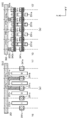
- FIGS. 13 to 16 are views showing the structure of a semiconductor device provided with a CFET
- FIG. 13 is a sectional view in the X direction
- FIG. 14 is a sectional view of a gate portion in the Y direction
- FIG. 15 is a source / drain in the Y direction.
- a cross-sectional view of the portion, FIG. 16 is a plan view.
- the X direction is the direction in which the nanowires extend
- the Y direction is the direction in which the gate extends
- the Z direction is the direction perpendicular to the substrate surface.
- FIGS. 13 to 16 are schematic views, and the dimensions and positions of the respective parts are not necessarily consistent.
- an element separation region 302 is formed on the surface of a semiconductor substrate 301 such as a silicon (Si) substrate, and the element active region 30a is defined by the element separation region 302.
- a semiconductor substrate 301 such as a silicon (Si) substrate
- the element active region 30a is defined by the element separation region 302.
- an N-type FET is formed on the P-type FET.
- a laminated transistor structure 390a is formed on the semiconductor substrate 301.
- the laminated transistor structure 390a includes a gate structure 391 formed on the semiconductor substrate 301.
- the gate structure 391 includes a gate electrode 356, a plurality of nanowires 358, a gate insulating film 355, and an insulating film 357.
- the gate electrode 356 extends in the Y direction and rises in the Z direction.
- the nanowires 358 penetrate the gate electrode 356 in the X direction and are arranged in the Y and Z directions.
- the gate insulating film 355 is formed between the gate electrode 356 and the nanowire 358.
- the gate electrode 356 and the gate insulating film 355 are formed at positions recessed from both ends of the nanowire 358 in the X direction, and the insulating film 357 is formed at the recessed portions.
- Insulating films 316 are formed on the semiconductor substrate 301 on both sides of the insulating film 357.
- Reference numerals 321 and 322 are interlayer insulating films.
- the gate electrode 356 is connected to the upper layer wiring by the via 385 provided in the opening 375.
- titanium, titanium nitride, polycrystalline silicon, or the like can be used for the gate electrode 356.
- a high dielectric constant material such as hafnium oxide, aluminum oxide, or oxides of hafnium and aluminum can be used for the gate insulating film 355.
- silicon or the like can be used for the nanowire 358.
- silicon oxide, silicon nitride, or the like can be used for the insulating film 316 and the insulating film 357.
- the number of nanowires 358 arranged in the Z direction is 4, and in the element active region 30a, a p-type semiconductor layer 331p is formed at each end of the two nanowires 358 on the semiconductor substrate 301 side. ..
- Two local wirings 386 in contact with the p-type semiconductor layer 331p are formed so as to sandwich the gate structure 391 in the X direction.
- an n-type semiconductor layer 341n is formed at each end of the two nanowires 358 on the side separated from the semiconductor substrate 101.
- Two local wirings 388 in contact with the n-type semiconductor layer 341n are formed so as to sandwich the gate structure 391 in the X direction.
- An insulating film 332 is formed between the local wiring 386 and the local wiring 388.
- An insulating film 389 is formed on the local wiring 388.
- the p-type semiconductor layer 331p is a p-type SiGe layer
- the n-type semiconductor layer 341n is an n-type Si layer.
- silicon oxide, silicon nitride, or the like can be used for the insulating film 332.
- the local wiring 388 is connected to the embedded wiring 3101 via the via 3071.
- the local wiring 386 is connected to the embedded wiring 3102 via the via 3072.
- the laminated transistor structure 390a has a P-type FET including a gate electrode 356, nanowires 358, a gate insulating film 355, and a P-type semiconductor layer 331p.
- a P-type FET including a gate electrode 356, nanowires 358, a gate insulating film 355, and a P-type semiconductor layer 331p.
- one P-type semiconductor layer 331p functions as a source region
- the other P-type semiconductor layer 331p functions as a drain region
- nanowire 358 functions as a channel.
- the laminated transistor structure 390a also has an N-type FET including a gate electrode 356, nanowires 358, a gate insulating film 355, and an N-type semiconductor layer 341n.
- one N-type semiconductor layer 341n functions as a source region
- the other N-type semiconductor layer 341n functions as a drain region
- nanowire 358 functions as a channel.
- wiring between transistors is performed by vias and metal wiring, but these can be realized by a known wiring process.
- the number of nanowires in the P-type FET and the N-type FET is assumed to be four in the Y direction and two in the Z direction, respectively, for a total of eight, but the number of nanowires is limited to this. It is not something that can be done. Further, the number of nanowires of the P-type FET and the N-type FET may be different.
- the semiconductor layer portion formed at both ends of the nanowire and forming the terminal serving as the source or drain of the transistor is referred to as a "pad".
- the p-type semiconductor layer 331p and the n-type semiconductor layer 341n correspond to pads.
- each insulating film and the like may be omitted.
- the nanowires and the pads on both sides thereof may be described in a simplified linear shape.
- expressions such as "same size” and the like that mean that the sizes and the like are the same include a range of manufacturing variation.
- the source and drain of the transistor may be referred to as a transistor node.
- FIG. 1 is a circuit diagram showing a configuration of a mask ROM as an example of a semiconductor storage device.
- the mask ROM of FIG. 1 whether the source and drain of the memory cell transistor are connected to the same line of the bit line and the ground power supply wiring or are connected to different lines, "1" "" of the stored data It corresponds to "0".
- the mask ROM includes a memory cell array 3, a column decoder 2, and a sense amplifier 18.
- the gates of the memory cells Mij are connected to the word line WLi in common in the row direction.
- the source and drain of the memory cell Mij are connected to the bit line BLj or connected to the ground power supply wiring VSS.
- the storage data of the memory cell Mij is set to “0”, one of the source and drain is connected to the bit line BLj and the other is connected to the ground power supply wiring VSS.
- the stored data of the memory cell Mij is set to "1”
- both the source and the drain are connected to the bit line BLj or the ground power supply wiring VSS.
- the column decoder 2 is composed of an N-type MOS transistor Cj.
- the drains are all connected in common, the gate is connected to the column selection signal line CLj, and the source is connected to the bit line BLj.
- the sense amplifier 18 includes a P-type MOS transistor 5 for precharging, an inverter 8 for determining the output data of the memory cell Mij, and an inverter 9 for buffering the output signal of the inverter 8.
- a precharge signal NPR is input to the gate of the P-type MOS transistor 5, a power supply voltage VDD is supplied to the source, and the drain is connected to the common drain of the N-type MOS transistor Cj.
- the inverter 8 receives the signal SIN of the common drain of the N-type MOS transistor Cj and determines the output data of the memory cell Mij.
- the inverter 9 receives the output signal SOUT of the inverter 8 and outputs the stored data of the memory cell Mij.
- the precharge signal NPR is changed from high level to low level, and the precharge P-type MOS transistor 5 is turned on.
- one of the source and the drain is connected to the bit line BL0, and the other is connected to the ground power supply wiring VSS. Therefore, since a current flows from the bit line BL0 to the ground power supply wiring VSS via the memory cell M00, the input signal SIN of the inverter 8 becomes a voltage lower than the switching level of the inverter 8. Therefore, the output signal SOUT of the inverter 8 holds the high level, and the output signal OUT of the inverter 9 holds the low level.
- the word line WL1 is changed from the low level in the non-selected state to the high level in the selected state.
- both the source and the drain are connected to the bit line BL0. Therefore, since no current flows through the bit line BL0, the input signal SIN of the inverter 8 has a voltage higher than the switching level of the inverter 8. Therefore, the output signal SOUT of the inverter 8 becomes a low level, and the output signal OUT of the inverter 9 becomes a high level.
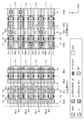
- FIGS. 2 (a) and 2 (b) are plan views of memory cells
- FIGS. 3 (a) to 3 (c) are shown. Is a cross-sectional view of the memory cell in the vertical direction in a plan view.
- FIG. 2A shows an upper portion, that is, a portion including a three-dimensional structure transistor (here, an N-type nanowire FET) formed on a side far from the substrate
- FIG. 2B shows a lower portion, that is, a substrate.
- a portion including a three-dimensional structure transistor (here, an N-type nanowire FET) formed on the near side is shown.
- FIG. 3A is a cross section of line Y1-Y1'
- FIG. 3B is a cross section of line Y2-Y2'
- FIG. 3C is a cross section of line Y3-Y3'.
- the horizontal direction of the drawing is the X direction (corresponding to the first direction)
- the vertical direction of the drawing is the Y direction (corresponding to the second direction)
- the direction perpendicular to the substrate surface It is in the Z direction (corresponding to the depth direction).
- the X direction is the direction in which the gate wiring and the word line extend
- the Y direction is the direction in which the nanowire and the bit wire extend. That is, in the drawings of each embodiment, the XY directions are opposite to those in FIGS. 13 to 16.
- the grids are evenly spaced in the X direction and evenly spaced in the Y direction.
- the grid spacing may be the same or different in the X direction and the Y direction. Further, the grid spacing may be different for each layer.
- each component does not necessarily have to be placed on the grid. However, from the viewpoint of suppressing manufacturing variations, it is preferable that the parts are arranged on the grid.
- memory cell storage values "0" and "1" are attached.
- FIG. 2 corresponds to the layout of 16-bit memory cells in which four in the horizontal direction and four in the vertical direction are arranged in the memory cell array 3 of FIG.
- Transistors connected to the bit lines BL0 and BL2 are formed in the lower part shown in FIG. 2B, and transistors connected to the bit lines BL1 and BL3 are formed in the upper part shown in FIG. 2A.
- the dashed line indicates the frame of the memory cell.
- power supply wirings 11, 12, 13, and 14 extending in the Y direction are provided at both ends of the memory cell in the X direction.
- the power supply wirings 11, 12, 13 and 14 are all embedded power supply wirings (BPR: Buried Power Rail) formed in the embedded wiring layer.
- BPR Buried Power Rail
- the power supply wirings 11, 12, 13 and 14 all supply the power supply voltage VSS.
- wirings 61, 62, 63, 64 extending in the Y direction are formed in the M1 wiring layer.
- the M1 wiring 61 corresponds to the bit wire BL0
- the M1 wiring 62 corresponds to the bit wire BL1
- the M1 wiring 63 corresponds to the bit wire BL2
- the M1 wiring 64 corresponds to the bit wire BL3.
- the layout structure of the memory cells in the left column of the drawing that is, the memory cells provided for the bit lines BL0 and BL1 will be described below.
- the layout structure of the memory cells in the right column of the drawing that is, the memory cells provided for the bit lines BL2 and BL3 is the same as the memory cells in the left column of the drawing except that the connection destinations of the transistor nodes are different. ..
- Nanowires 21a, 21b, 21c, 21d extending in the Y direction are formed in the lower part of the memory cell, and nanowires 26a, 26b, 26c, 26d extending in the Y direction are formed in the upper part of the memory cell.
- the nanowires 21a and 26a overlap in a plan view
- the nanowires 21b and 26b overlap in a plan view
- the nanowires 21c and 26c overlap in a plan view
- the nanowires 21d and 26d overlap in a plan view.
- Pads 22a, 22b, 22c, 22d which are doped with N-type semiconductors, on the lower side of the drawing of the nanowire 21a, between the nanowires 21a and 21b, between the nanowires 21b and 21c, between the nanowires 21c and 21d, and on the upper side of the drawing of the nanowire 21d. 22e are formed respectively.
- Pads 27a, 27b, 27c, 27d which are doped with N-type semiconductors, on the lower side of the drawing of the nanowire 26a, between the nanowires 26a and 26b, between the nanowires 26b and 26c, between the nanowires 26c and 26d, and on the upper side of the drawing of the nanowire 26d. 27e are formed respectively.
- the nanowires 21a form the channel portion of the N-type transistor M00, and the pads 22a and 22b form the nodes of the N-type transistor M00.
- the nanowires 21b form the channel portion of the N-type transistor M10, and the pads 22b and 22c form the nodes of the N-type transistor M10.
- the pad 22b is shared by the N-type transistors M00 and M10.
- the nanowires 21c form the channel portion of the N-type transistor M20, and the pads 22c and 22d form the nodes of the N-type transistor M20.
- the pad 22c is shared by the N-type transistors M10 and M20.
- the nanowires 21d form the channel portion of the N-type transistor M30, and the pads 22d and 22e form the nodes of the N-type transistor M30.
- the pad 22d is shared by the N-type transistors M20 and M30.
- the nanowire 26a constitutes the channel portion of the N-type transistor M01, and the pads 27a and 27b form the node of the N-type transistor M01.
- the nanowires 26b form the channel portion of the N-type transistor M11, and the pads 27b and 27c form the nodes of the N-type transistor M11.
- the pad 27b is shared by the N-type transistors M01 and M11.
- the nanowires 26c form the channel portion of the N-type transistor M21, and the pads 27c and 27d form the nodes of the N-type transistor M21.
- the pad 27c is shared by the N-type transistors M11 and M21.
- the nanowires 26d form the channel portion of the N-type transistor M31, and the pads 27d and 27e form the nodes of the N-type transistor M31.
- the pad 27d is shared by the N-type transistors M21 and M31.
- the N-type transistors M00, M10, M20, and M30 are formed above the embedded wiring layer in the Z direction, and the N-type transistors M01, M11, M21, and M31 are N-type transistors M00, M10, and M20 in the Z direction. , M30 is formed above.
- the gate wirings 31a, 31b, 31c, 31d extend in the X direction and extend in the Z direction from the lower part to the upper part of the memory cell.
- the gate wiring 31a serves as a gate for the N-type transistors M00 and M01. That is, the nanowire 21a, the gate wiring 31a, and the pads 22a and 22b constitute the N-type transistor M00.
- the nanowire 26a, the gate wiring 31a, and the pads 27a and 27b constitute the N-type transistor M01.
- the gate wiring 31b serves as a gate for the N-type transistors M10 and M11
- the gate wiring 31c serves as a gate for the N-type transistors M20 and M21
- the gate wiring 31d serves as a gate for the N-type transistors M30 and M31.
- the gate wirings 31a, 31b, 31c, and 31d are connected to the word lines WL0, WL1, WL2, and WL3, respectively.
- Local wirings 41a, 41b, 41c, 41d, 41e extending in the X direction are formed in the lower part of the memory cell.
- the local wirings 41a, 41b, 41c, 41d, 41e are connected to the pads 22a, 22b, 22c, 22d, 22e, respectively, and extend from the pads 22a, 22b, 22c, 22d, 22e to the left in the drawing.
- Local wirings 43a, 43b, 43c, 43d, 43e extending in the X direction are formed in the upper part of the memory cell.
- the local wirings 43a, 43b, 43c, 43d, 43e are connected to the pads 27a, 27b, 27c, 27d, 27e, respectively, and extend from the pads 27a, 27b, 27c, 27d, 27e to the right in the drawing.
- the local wirings 41a, 41d, 41e are connected to the power supply wiring 11 via the contacts 51a, 51b, 51c.
- the local wirings 41b and 41c are connected to the M1 wiring 61 via the contacts 52a and 52b. That is, in the N-type transistors M00 and M20, one node is connected to the power supply wiring 11 and the other node is connected to the M1 wiring 61. In the N-type transistor M10, both nodes are connected to the M1 wiring 61. In the N-type transistor M30, both nodes are connected to the power supply wiring 11.
- the local wirings 43b and 43e are connected to the power supply wiring 12 via the contacts 53a and 53b.
- the local wirings 43a, 43c, 43d are connected to the M1 wiring 62 via the contacts 54a, 54b, 54c. That is, in the N-type transistors M01, M11, and M31, one node is connected to the power supply wiring 12 and the other node is connected to the M1 wiring 62. In the N-type transistor M21, both nodes are connected to the M1 wiring 62.
- the ROM memory cell corresponds to the three-dimensional structure transistor M00 provided between the M1 wiring 61 corresponding to the bit line BL0 and the power supply wiring 11 for supplying VSS, and the bit line BL1.
- a three-dimensional structure transistor M01 provided between the M1 wiring 62 and the power supply wiring 12 for supplying the VSS is provided.
- the transistor M01 is formed on the upper layer of the transistor M00, and the channel portion overlaps with the transistor M00 in a plan view. Then, in the ROM memory cell, the first data is obtained depending on whether the connection destinations of the local wirings 41a and 41b connected to the source and drain of the transistor M00 are the same line or different lines of the M1 wiring 61 and the power supply wiring 11.
- the second data is obtained depending on whether the connection destinations of the local wirings 43a and 43b connected to the source and drain of the transistor M01 are the same line or different lines of the M1 wiring 62 and the power supply wiring 12, respectively. It will be remembered. As a result, it is possible to realize a layout structure having a small area for the mask ROM.
- the upper transistor and the lower transistor are both N-type transistors, and separate memory cells are formed.
- the nodes of the transistors of the adjacent memory cells are shared in the Y direction. As a result, the area of the semiconductor storage device can be reduced.
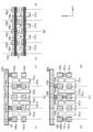
- FIG. 4 is an example of the layout structure of the inverter cell using the CFET.
- the upper transistor N1 shown in FIG. 4A is N-type
- the lower transistor P1 shown in FIG. 4B is P-type.
- the transistor P1 and the transistor N1 are connected in series between the power supply wiring 611 for supplying VDD and the power supply wiring 612 for supplying VSS.
- the transistor P1 has nanowires 621 as a channel portion and pads 622a and 622b.
- the transistor N1 has nanowires 626 as a channel portion and pads 627a and 627b.
- the gate wiring 631 serves as a common gate for the transistor P1 and the transistor N1.
- the M1 wiring 661 which is the input of the inverter, is connected to the gate wiring 631.
- the M1 wiring 662 which is the output of the inverter, is connected to the local wirings 642 and 644 connected to the drains of the transistor P1 and the transistor N1.
- both the lower part and the upper part form N-type transistors. That is, in the semiconductor chip having the mask ROM according to the present embodiment, the lower part of the CFET includes a region which is a P-type transistor and a region which is an N-type transistor.
- the transistor at the lower part may be manufactured as follows, for example. That is, when forming the transistor in the lower part, the portion of the N-type transistor is masked and the other portion is doped into the P conductive type. After that, the portion other than the N-type transistor is masked and the N-conducting type is doped. By arranging the N-type transistor and the P-type transistor apart from each other, it is possible to reliably perform P-conductive doping and N-conductive doping.
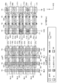
- FIGS. 5 and 6 are views showing an example of the layout structure of the mask ROM according to the second embodiment
- FIGS. 5 (a) and 5 (b) are plan views of memory cells
- FIGS. 6 (a) to 6 (c) are shown. Is a cross-sectional view of the memory cell in the vertical direction in a plan view. Specifically, FIG. 5A shows the upper part, and FIG. 5B shows the lower part. 6 (a) is a cross section of line Y1-Y1'
- FIG. 6 (b) is a cross section of line Y2-Y2'
- FIG. 6 (c) is a cross section of line Y3-Y3'.
- FIG. 5 corresponds to the layout of 8-bit memory cells in which two are arranged in the horizontal direction and four are arranged in the vertical direction in the memory cell array 3 of FIG.
- the dashed line indicates the frame of the memory cell.
- wirings 161, 162, 163, 164 extending in the Y direction are formed in the M1 wiring layer.
- the wirings 161, 163 supply the power supply voltage VSS, the wiring 162 corresponds to the bit line BL0, and the wiring 164 corresponds to the bit line BL1.
- the layout structure of the memory cells in the left column of the drawing that is, the memory cells provided for the bit line BL0 will be described below.
- the layout structure of the memory cells in the right column of the drawing that is, the memory cells provided for the bit line BL1 is the same as that of the memory cells in the left column of the drawing, except that the connection destinations of the transistor nodes are different.
- Nanowires 121a, 121b, 121c, 121d extending in the Y direction are formed in the lower part of the memory cell, and nanowires 126a, 126b, 126c, 126d extending in the Y direction are formed in the upper part of the memory cell.
- the nanowires 121a and 126a overlap in a plan view
- the nanowires 121b and 126b overlap in a plan view
- the nanowires 121c and 126c overlap in a plan view
- the nanowires 121d and 126d overlap in a plan view.
- Pads 122a, 122b, 122c, 122d which are doped with N-type semiconductors, on the lower side of the drawing of the nanowire 121a, between the nanowires 121a and 121b, between the nanowires 121b and 121c, between the nanowires 121c and 121d, and on the upper side of the drawing of the nanowire 121d, 122e are formed respectively.
- Pads 127a, 127b, 127c, 127d which are doped with N-type semiconductors, on the lower side of the drawing of the nanowire 126a, between the nanowires 126a and 126b, between the nanowires 126b and 126c, between the nanowires 126c and 126d, and on the upper side of the drawing of the nanowire 126d, 127e are formed respectively.
- the nanowires 121a and 126a form the channel portion of the N-type transistor M00, and the pads 122a, 122b, 127a and 127b form the node of the N-type transistor M00.
- the nanowires 121b and 126b form the channel portion of the N-type transistor M10, and the pads 122b, 122c, 127b and 127c form the node of the N-type transistor M10.
- the pads 122b and 127b are shared by the N-type transistors M00 and M10.
- the nanowires 121c and 126c form the channel portion of the N-type transistor M20, and the pads 122c, 122d, 127c and 127d form the node of the N-type transistor M20.
- the pads 122c and 127c are shared by the N-type transistors M10 and M20.
- the nanowires 121d and 126d form the channel portion of the N-type transistor M30, and the pads 122d, 122e, 127d and 127e form the node of the N-type transistor M30.
- the pads 122d and 127d are shared by the N-type transistors M20 and M30.
- the gate wirings 131a, 131b, 131c, 131d extend in the X direction and extend in the Z direction from the lower part to the upper part of the memory cell.
- the gate wiring 131a serves as a gate for the N-type transistor M00. That is, the nanowires 121a, 126a, the gate wiring 131a, and the pads 122a, 122b, 127a, 127b constitute the N-type transistor M00.
- the gate wiring 131b serves as the gate of the N-type transistor M10
- the gate wiring 131c serves as the gate of the N-type transistor M20
- the gate wiring 131d serves as the gate of the N-type transistor M30.
- the gate wirings 131a, 131b, 131c, 131d are connected to the word lines WL0, WL1, WL2, and WL3, respectively.
- Local wirings 141a, 141b, 141c, 141d, 141e extending in the X direction are formed in the lower part of the memory cell.
- the local wirings 141a, 141b, 141c, 141d, 141e are connected to the pads 122a, 122b, 122c, 122d, 122e, respectively, and extend from the pads 122a, 122b, 122c, 122d, 122e to the left and right sides of the drawing.
- Local wirings 143a, 143b, 143c, 143d, 143e extending in the X direction are formed in the upper part of the memory cell.
- the local wirings 143a, 143b, 143c, 143d, and 143e are connected to the pads 127a, 127b, 127c, 127d, and 127e, respectively, and extend from the pads 127a, 127b, 127c, 127d, and 127e to the left and right sides of the drawing.
- the local wirings 141a and 143a are connected to each other via the contact 151a.
- the local wirings 141b and 143b are connected to each other via the contact 151b.
- the local wirings 141c and 143c are connected to each other via the contact 151c.
- the local wirings 141d and 143d are connected to each other via the contact 151d.
- the local wirings 141e and 143e are connected to each other via the contact 151e.
- the local wirings 143a, 143d, and 143e are connected to the M1 wiring 161 via the contacts 152a, 152b, and 153c.
- the local wirings 143b and 143c are connected to the M1 wiring 162 via the contacts 153a and 153b. That is, in the N-type transistors M00 and M20, one node is connected to the M1 wiring 161 and the other node is connected to the M1 wiring 162. In the N-type transistor M10, both nodes are connected to the M1 wiring 162. In the N-type transistor M30, both nodes are connected to the M1 wiring 161.
- the ROM memory cell is a three-dimensional structure transistor provided between the M1 wiring 162 corresponding to the bit line BL0 and the M1 wiring 161 for supplying VSS, and constitutes the N-type transistor M00. It includes first and second transistors. The second transistor is formed on the upper layer of the first transistor, and the channel portion overlaps with the first transistor in a plan view.
- the local wiring 141a connected to the source of the first transistor and the local wiring 143a connected to the source of the second transistor are connected to each other.
- the local wiring 141b connected to the drain of the first transistor and the local wiring 143b connected to the drain of the second transistor are connected to each other.
- the ROM memory cell stores data depending on whether the connection destinations of the local wirings 141a and 143a and the local wirings 141b and 143b are the same line or different lines of the M1 wiring 162 and the M1 wiring 161. As a result, it is possible to realize a layout structure having a small area for the mask ROM.
- the memory cell for one bit is composed of two transistors formed in the upper part and the lower part, the drive capacity is larger than that in the first embodiment and the operation is performed at high speed. Further, when the characteristics of the transistor vary between the upper part and the lower part, the characteristics vary for each bit line in the first embodiment, but the variation does not affect the present embodiment. Further, since the storage value of the memory cell is set by the contact of the higher layer as compared with the first embodiment, the manufacturing period for changing the storage value of the memory cell can be shortened. On the other hand, in the first embodiment, the area of the memory cell array can be reduced as compared with the present embodiment.
- the wiring for supplying the power supply voltage VSS is arranged between the bit wires, the crosstalk noise between the bit wires can be suppressed. As a result, the operation is stable.
- the positions of the contacts that connect the nodes of the upper and lower transistors that make up the memory cell are arranged in a zigzag pattern. As a result, the distance between the contacts can be increased, so that the ease of manufacturing is improved, the yield is improved, and the reliability of the semiconductor storage device is improved.
- FIGS. 7 and 8 are diagrams showing an example of the layout structure of the mask ROM according to the modified example of the second embodiment
- FIGS. 7 (a) and 7 (b) are plan views of the memory cells
- (C) is a cross-sectional view of the memory cell in the vertical direction in a plan view.
- FIG. 7A shows the upper part
- FIG. 7B shows the lower part.
- 8 (a) is a cross section of line Y1-Y1'
- FIG. 8 (b) is a cross section of line Y2-Y2'
- FIG. 8 (c) is a cross section of line Y3-Y3'.
- FIGS. 7 and 8 the components common to those in FIGS. 5 and 6 are designated by the same reference numerals, and detailed description thereof may be omitted here.
- power supply wirings 111 and 112 extending in the Y direction are provided at the left end of the drawing of the memory cell.
- Both the power supply wirings 111 and 112 are embedded power supply wirings (BPR: Buried Power Rail) formed in the embedded wiring layer. Both the power supply wirings 111 and 112 supply the power supply voltage VSS.
- the local wirings 141a, 141d, 141e are connected to the power supply wiring 111 via the contacts 154a, 154b, 154c.
- the local wirings 143b and 143c are connected to the M1 wiring 162 via the contacts 153a and 153b. That is, in the N-type transistors M00 and M20, one node is connected to the power supply wiring 111 and the other node is connected to the M1 wiring 162. In the N-type transistor M10, both nodes are connected to the M1 wiring 162. In the N-type transistor M30, both nodes are connected to the power supply wiring 111.
- M1 wirings 161 and 163 are not connected to memory cells and function to reduce crosstalk noise between bit lines.
- the power supply wirings 111 and 112 for supplying VSS extend in the Y direction at the left end of the drawing of the memory cell, but the power supply wiring for supplying VSS may be provided at the right end of the drawing of the memory cell so as to extend in the Y direction. It doesn't matter. In this case, the position of the contact for connection to the power supply wiring is also on the right side of the memory cell drawing. Further, the power supply wiring for supplying VSS may be provided at both the left end and the right end of the drawing of the memory cell. In this case, the position of the contact for connection to the power supply wiring may be either the left side or the right side of the drawing of the memory cell.
- FIGS. 9 and 10 are views showing an example of the layout structure of the mask ROM according to the third embodiment
- FIGS. 9 (a) and 9 (b) are plan views of memory cells
- FIGS. 10 (a) and 10 (b) are shown. Is a cross-sectional view of the memory cell in the vertical direction in a plan view. Specifically, FIG. 9A shows the upper part, and FIG. 9B shows the lower part.
- FIG. 10A is a cross section of line Y1-Y1', and FIG. 10B is a cross section of line Y2-Y2'.
- FIG. 9 corresponds to the layout of 8 bits of memory cells in which two are arranged in the horizontal direction and four are arranged in the vertical direction in the memory cell array 3 of FIG.
- a memory cell for one bit is formed by two N-type transistors arranged in the X direction formed in the upper part shown in FIG. 9A.
- the dashed line indicates the frame of the memory cell.
- wirings 261,262,263,264 extending in the Y direction are formed in the M1 wiring layer.
- the wiring 261 corresponds to the bit line BL0, 262 and 264 supply the power supply voltage VSS, and the wiring 263 corresponds to the bit line BL1.
- Nanowires 221a, 221b, 221c, 221d extending in the Y direction are formed in the lower part of the memory cell. Further, the nanowires 223a, 223b, 223c, and 223d extending in the Y direction are formed so as to be aligned with the nanowires 221a, 221b, 221c, and 221d in the X direction, respectively. Nanowires 226a, 226b, 226c, and 226d extending in the Y direction are formed on the upper part of the memory cell.
- the nanowires 228a, 228b, 228c, and 228d extending in the Y direction are formed so as to line up with the nanowires 226a, 226b, 226c, and 226d in the X direction, respectively.
- the nanowires 221a and 226a overlap in a plan view
- the nanowires 221b and 226b overlap in a plan view
- the nanowires 221c and 226c overlap in a plan view
- the nanowires 221d and 226d overlap in a plan view.
- the nanowires 223a and 228a overlap in a plan view
- the nanowires 223b and 228b overlap in a plan view
- the nanowires 223c and 228c overlap in a plan view
- the nanowires 223d and 228d overlap in a plan view.
- Pads 222a, 222b, 222c, 222d which are doped with N-type semiconductors, on the lower side of the drawing of nanowire 221a, between nanowires 221a and 221b, between nanowires 221b and 221c, between nanowires 221c and 221d, and on the upper side of the drawing of nanowire 221d. 222e are formed respectively.
- Pads 224a, 224b, 224c, 224d which are doped with N-type semiconductors, on the lower side of the drawing of nanowire 223a, between nanowires 223a and 223b, between nanowires 223b and 223c, between nanowires 223c and 223d, and on the upper side of the drawing of nanowire 223d.
- 224e are formed respectively.
- Pads 227a, 227b, 227c, 227d 227e are formed respectively.
- Pads 229a, 229b, 229c, 229d 229e are formed respectively.
- nanowires 221a and 223a form a channel portion of the N-type transistor M00, and pads 222a, 222b, 224a and 224b form a node of the N-type transistor M00.
- the nanowires 221b and 223b form the channel portion of the N-type transistor M10, and the pads 222b, 222c, 224b and 224c form the nodes of the N-type transistor M10.
- the pads 222b and 224b are shared by the N-type transistors M00 and M10.
- the nanowires 221c and 223c form the channel portion of the N-type transistor M20, and the pads 222c, 222d, 224c and 224d form the node of the N-type transistor M20.
- the pads 222c and 224c are shared by the N-type transistors M10 and M20.
- the nanowires 221d and 223d form the channel portion of the N-type transistor M30, and the pads 222d, 222e, 224d and 224e form the nodes of the N-type transistor M30.
- the pads 222d and 224d are shared by the N-type transistors M20 and M30.
- nanowires 226a and 228a form a channel portion of the N-type transistor M01, and pads 227a, 227b, 229a and 229b form a node of the N-type transistor M01.
- the nanowires 226b and 228b form the channel portion of the N-type transistor M11, and the pads 227b, 227c, 229b and 229c form the nodes of the N-type transistor M11.
- the pads 227b and 229b are shared by the N-type transistors M01 and M11.
- the nanowires 226c and 228c form the channel portion of the N-type transistor M21, and the pads 227c, 227d, 229c and 229d form the node of the N-type transistor M21.
- the pads 227c and 229c are shared by the N-type transistors M11 and M21.
- the nanowires 226d and 228d form the channel portion of the N-type transistor M31, and the pads 227d, 227e, 229d and 229e form the nodes of the N-type transistor M31.
- the pads 227d and 229d are shared by the N-type transistors M21 and M31.
- the gate wirings 231a, 231b, 231c, and 231d extend in the X direction and extend in the Z direction from the lower part to the upper part of the memory cell.
- the gate wiring 231a serves as a gate for the N-type transistors M00 and M01. That is, the nanowires 221a, 223a, the gate wiring 231a, and the pads 222a, 222b, 224a, 224b constitute the N-type transistor M00. Further, the nanowires 226a and 228a, the gate wiring 231a, and the pads 227a, 227b, 229a and 229b constitute the N-type transistor M01.
- the gate wiring 231b serves as a gate for the N-type transistors M10 and M11
- the gate wiring 231c serves as a gate for the N-type transistors M20 and M21
- the gate wiring 231d serves as a gate for the N-type transistors M30 and M31.
- the gate wirings 231a, 231b, 231c, and 231d are connected to the word lines WL0, WL1, WL2, and WL3, respectively.
- Local wirings 241a, 241b, 241c, 241d, 241e extending in the X direction are formed in the lower part of the memory cell.
- the local wiring 241a is connected to the pads 222a and 224a, and extends from the pads 222a and 224a on both the left and right sides of the drawing.
- the local wiring 241b is connected to the pads 222b and 224b, and extends from the pads 222b and 224b on both the left and right sides of the drawing.
- the local wiring 241c is connected to the pads 222c and 224c, and extends from the pads 222c and 224c on both the left and right sides of the drawing.
- the local wiring 241d is connected to the pads 222d and 224d, and extends from the pads 222d and 224d on both the left and right sides of the drawing.
- the local wiring 241e is connected to the pads 222e and 224e, and extends from the pads 222e and 224e on both the left and right sides of the drawing.
- Local wirings 243a, 243b, 243c, 243d, 243e extending in the X direction are formed in the upper part of the memory cell.
- the local wiring 243a is connected to the pads 227a and 229a.
- the local wiring 243b is connected to the pads 227b and 229b.
- the local wiring 243c is connected to the pads 227c and 229c.
- the local wiring 243d is connected to the pads 227d and 229d.
- the local wiring 243e is connected to the pads 227e and 229e.
- the local wirings 241b and 241c are connected to the M1 wiring 261 via the contacts 251a and 251b.
- the local wirings 241a, 241d, and 241e are connected to the M1 wiring 264 via the contacts 252a, 252b, and 252c. That is, in the N-type transistors M00 and M20, one node is connected to the M1 wiring 261 and the other node is connected to the M1 wiring 264. In the N-type transistor M10, both nodes are connected to the M1 wiring 261. In the N-type transistor M30, both nodes are connected to the M1 wiring 264.
- the local wirings 243b and 243e are connected to the M1 wiring 262 via the contacts 253a and 253b.
- the local wirings 243a, 243c, 243d are connected to the M1 wiring 263 via the contacts 254a, 254b, 254c. That is, in the N-type transistors M01, M11, and M31, one node is connected to the M1 wiring 262 and the other node is connected to the M1 wiring 263. In the N-type transistor M21, both nodes are connected to the M1 wiring 263.
- the ROM memory cell corresponds to the three-dimensional structure transistor M00 provided between the M1 wiring 261 corresponding to the bit line BL0 and the M1 wiring 264 supplying VSS, and the bit line BL1.
- a three-dimensional structure transistor M01 provided between the M1 wiring 263 to be used and the M1 wiring 262 to supply the VSS is provided.
- the transistors M00 and M01 are both composed of two transistors arranged in the X direction and connected in parallel.
- the transistor M01 is formed on the upper layer of the transistor M00, and the channel portion overlaps with the transistor M00 in a plan view.
- the first data is obtained depending on whether the connection destinations of the local wirings 241a and 241b connected to the source and drain of the transistor M00 are the same line or different lines of the M1 wiring 261 and the M1 wiring 264, respectively. It will be remembered. Further, in the ROM memory cell, the second data is obtained depending on whether the connection destinations of the local wirings 243a and 243b connected to the source and drain of the transistor M01 are the same line or different lines of the M1 wiring 263 and the M1 wiring 262, respectively. It will be remembered. As a result, it is possible to realize a layout structure having a small area for the mask ROM.
- the memory cells for one bit are arranged in the X direction and composed of two transistors connected in parallel, the drive capacity is large and the operation is high speed as compared with the first embodiment.
- the transistors constituting the memory cell are assumed to include two transistors connected in parallel, but may include three or more transistors connected in parallel.
- FIGS. 11 and 12 are diagrams showing an example of the layout structure of the mask ROM according to the modified example of the third embodiment
- FIGS. 11 (a) and 12 (b) are plan views of the memory cells
- (D) is a cross-sectional view of the memory cell in the vertical direction in a plan view.
- FIG. 11A shows the upper part
- FIG. 11B shows the lower part.
- 12 (a) is a cross section of line Y1-Y1'
- FIG. 12 (b) is a cross section of line Y2-Y2'
- FIG. 12 (c) is a cross section of line Y3-Y3'
- FIG. 12 (d) is line Y4. -Y4'cross section.
- FIGS. 11 and 12 the components common to those in FIGS. 9 and 10 are designated by the same reference numerals, and detailed description thereof may be omitted here.
- power supply wirings 211 and 212 extending in the Y direction are provided at both ends of the memory cell in the X direction.
- Both the power supply wirings 211 and 212 are embedded power supply wirings (BPR: Buried Power Rail) formed in the embedded wiring layer.
- BPR Buried Power Rail
- Both the power supply wirings 211 and 212 supply the power supply voltage VSS.
- the M1 wirings 262 and 264 that supply the power supply voltage VSS are not connected to the memory cells and function for reducing crosstalk noise between the bit lines.
- Local wirings 245a, 245b, 245c, 245d, 245e extending in the X direction are formed in the lower part of the memory cell.
- the local wiring 245a is connected to the pads 222a and 224a and extends from the pads 222a and 224a to the left side of the drawing.
- the local wiring 245b is connected to the pads 222b and 224b, and extends from the pads 222b and 224b to the left side of the drawing.
- the local wiring 245c is connected to the pads 222c and 224c and extends from the pads 222c and 224c to the left side of the drawing.
- the local wiring 245d is connected to the pads 222d and 224d, and extends from the pads 222d and 224d to the left side of the drawing.
- the local wiring 245e is connected to the pads 222e and 224e and extends from the pads 222e and 224e to the left side of the drawing.
- Local wirings 247a, 247b, 247c, 247d, 247e extending in the X direction are formed in the upper part of the memory cell.
- the local wiring 247a is connected to the pads 227a and 229a and extends from the pads 227a and 229a to the right side of the drawing.
- the local wiring 247b is connected to the pads 227b and 229b, and extends from the pads 227b and 229b to the right side of the drawing.
- the local wiring 247c is connected to the pads 227c and 229c, and extends from the pads 227c and 229c to the right side of the drawing.
- the local wiring 247d is connected to the pads 227d and 229d, and extends from the pads 227d and 229d to the right side of the drawing.
- the local wiring 247e is connected to the pads 227e and 229e and extends from the pads 227e and 229e to the right side of the drawing.
- the local wirings 245a, 245b, 245c, 245d, and 245e overlap with the power supply wiring 211 in a plan view, but do not overlap with the power supply wiring 212.
- the local wirings 247a, 247b, 247c, 247d, and 247e overlap the power supply wiring 212 in a plan view, but do not overlap the power supply wiring 211.
- the local wirings 245b and 245c are connected to the M1 wiring 261 via the contacts 251a and 251b.
- the local wirings 245a, 245d, 245e are connected to the power supply wiring 211 via the contacts 255a, 255b, 255c. That is, in the N-type transistors M00 and M20, one node is connected to the M1 wiring 261 and the other node is connected to the power supply wiring 211. In the N-type transistor M10, both nodes are connected to the M1 wiring 261. In the N-type transistor M30, both nodes are connected to the power supply wiring 211.
- the local wirings 247b and 247e are connected to the power supply wiring 212 via the contacts 256a and 256b.
- the local wirings 247a, 247c, 247d are connected to the M1 wiring 263 via the contacts 254a, 254b, 254c. That is, in the N-type transistors M01, M11, and M31, one node is connected to the power supply wiring 212 and the other node is connected to the M1 wiring 263. In the N-type transistor M21, both nodes are connected to the M1 wiring 263.
- the transistor is provided with one nanowire, but a part or all of the transistor may be provided with a plurality of nanowires.
- a plurality of nanowires may be provided in the X direction in a plan view, or a plurality of nanowires may be provided in the Z direction.
- a plurality of nanowires may be provided in both the X direction and the Z direction.
- the number of nanowires included in the transistor may be different between the upper part and the lower part of the cell.
- the cross-sectional shape of the nanowire is substantially square, but the present invention is not limited to this. For example, it may be circular or rectangular.
- a nanowire FET has been described as an example as a three-dimensional structure transistor, but the description is not limited to this.
- the transistor formed in the lower part of the cell may be a fin type transistor.
- a semiconductor integrated circuit device including a ROM memory cell using a CFET can realize a layout structure having a small area, which is useful for improving the performance of a semiconductor chip, for example.
Landscapes
- Semiconductor Memories (AREA)
Priority Applications (3)
| Application Number | Priority Date | Filing Date | Title |
|---|---|---|---|
| JP2021519380A JP7560747B2 (ja) | 2019-05-13 | 2020-05-01 | 半導体記憶装置 |
| US17/524,369 US12225719B2 (en) | 2019-05-13 | 2021-11-11 | Semiconductor storage device |
| US19/013,630 US20250151268A1 (en) | 2019-05-13 | 2025-01-08 | Semiconductor storage device |
Applications Claiming Priority (2)
| Application Number | Priority Date | Filing Date | Title |
|---|---|---|---|
| JP2019090699 | 2019-05-13 | ||
| JP2019-090699 | 2019-05-13 |
Related Child Applications (1)
| Application Number | Title | Priority Date | Filing Date |
|---|---|---|---|
| US17/524,369 Continuation US12225719B2 (en) | 2019-05-13 | 2021-11-11 | Semiconductor storage device |
Publications (1)
| Publication Number | Publication Date |
|---|---|
| WO2020230666A1 true WO2020230666A1 (ja) | 2020-11-19 |
Family
ID=73289101
Family Applications (1)
| Application Number | Title | Priority Date | Filing Date |
|---|---|---|---|
| PCT/JP2020/018393 Ceased WO2020230666A1 (ja) | 2019-05-13 | 2020-05-01 | 半導体記憶装置 |
Country Status (3)
| Country | Link |
|---|---|
| US (2) | US12225719B2 (https=) |
| JP (1) | JP7560747B2 (https=) |
| WO (1) | WO2020230666A1 (https=) |
Cited By (4)
| Publication number | Priority date | Publication date | Assignee | Title |
|---|---|---|---|---|
| WO2023157724A1 (ja) * | 2022-02-16 | 2023-08-24 | 株式会社ソシオネクスト | 半導体記憶装置 |
| WO2024018875A1 (ja) * | 2022-07-21 | 2024-01-25 | 株式会社ソシオネクスト | 半導体記憶装置 |
| WO2026004616A1 (ja) * | 2024-06-27 | 2026-01-02 | 株式会社ソシオネクスト | 半導体記憶装置 |
| WO2026053741A1 (ja) * | 2024-09-03 | 2026-03-12 | 株式会社ソシオネクスト | 半導体記憶装置および半導体集積回路装置 |
Families Citing this family (1)
| Publication number | Priority date | Publication date | Assignee | Title |
|---|---|---|---|---|
| EP4451332A3 (en) * | 2023-04-17 | 2025-01-01 | Samsung Electronics Co., Ltd. | Integrated circuit including read only memory (rom) cell |
Citations (4)
| Publication number | Priority date | Publication date | Assignee | Title |
|---|---|---|---|---|
| US7715246B1 (en) * | 2008-06-27 | 2010-05-11 | Juhan Kim | Mask ROM with light bit line architecture |
| JP2011258898A (ja) * | 2010-06-11 | 2011-12-22 | Toshiba Corp | 半導体装置およびその製造方法 |
| US20160329313A1 (en) * | 2014-06-23 | 2016-11-10 | Synopsys, Inc. | Cells having transistors and interconnects including nanowires or 2d material strips |
| US20180151576A1 (en) * | 2016-11-28 | 2018-05-31 | Samsung Electronics Co., Ltd. | Semiconductor devices |
Family Cites Families (6)
| Publication number | Priority date | Publication date | Assignee | Title |
|---|---|---|---|---|
| FR2749434B1 (fr) * | 1996-05-31 | 1998-09-04 | Dolphin Integration Sa | Matrice de memoire rom compacte |
| WO2017145906A1 (ja) * | 2016-02-25 | 2017-08-31 | 株式会社ソシオネクスト | 半導体集積回路装置 |
| US10453850B2 (en) * | 2016-07-19 | 2019-10-22 | Tokyo Electron Limited | Three-dimensional semiconductor device including integrated circuit, transistors and transistor components and method of fabrication |
| TWI739879B (zh) * | 2016-08-10 | 2021-09-21 | 日商東京威力科創股份有限公司 | 用於半導體裝置的延伸區域 |
| US10756097B2 (en) * | 2018-06-29 | 2020-08-25 | International Business Machines Corporation | Stacked vertical transistor-based mask-programmable ROM |
| US10720391B1 (en) * | 2019-01-04 | 2020-07-21 | Globalfoundries Inc. | Method of forming a buried interconnect and the resulting devices |
-
2020
- 2020-05-01 WO PCT/JP2020/018393 patent/WO2020230666A1/ja not_active Ceased
- 2020-05-01 JP JP2021519380A patent/JP7560747B2/ja active Active
-
2021
- 2021-11-11 US US17/524,369 patent/US12225719B2/en active Active
-
2025
- 2025-01-08 US US19/013,630 patent/US20250151268A1/en active Pending
Patent Citations (4)
| Publication number | Priority date | Publication date | Assignee | Title |
|---|---|---|---|---|
| US7715246B1 (en) * | 2008-06-27 | 2010-05-11 | Juhan Kim | Mask ROM with light bit line architecture |
| JP2011258898A (ja) * | 2010-06-11 | 2011-12-22 | Toshiba Corp | 半導体装置およびその製造方法 |
| US20160329313A1 (en) * | 2014-06-23 | 2016-11-10 | Synopsys, Inc. | Cells having transistors and interconnects including nanowires or 2d material strips |
| US20180151576A1 (en) * | 2016-11-28 | 2018-05-31 | Samsung Electronics Co., Ltd. | Semiconductor devices |
Cited By (4)
| Publication number | Priority date | Publication date | Assignee | Title |
|---|---|---|---|---|
| WO2023157724A1 (ja) * | 2022-02-16 | 2023-08-24 | 株式会社ソシオネクスト | 半導体記憶装置 |
| WO2024018875A1 (ja) * | 2022-07-21 | 2024-01-25 | 株式会社ソシオネクスト | 半導体記憶装置 |
| WO2026004616A1 (ja) * | 2024-06-27 | 2026-01-02 | 株式会社ソシオネクスト | 半導体記憶装置 |
| WO2026053741A1 (ja) * | 2024-09-03 | 2026-03-12 | 株式会社ソシオネクスト | 半導体記憶装置および半導体集積回路装置 |
Also Published As
| Publication number | Publication date |
|---|---|
| JP7560747B2 (ja) | 2024-10-03 |
| JPWO2020230666A1 (https=) | 2020-11-19 |
| US20250151268A1 (en) | 2025-05-08 |
| US12225719B2 (en) | 2025-02-11 |
| US20220068942A1 (en) | 2022-03-03 |
Similar Documents
| Publication | Publication Date | Title |
|---|---|---|
| JP7560747B2 (ja) | 半導体記憶装置 | |
| CN101939837B (zh) | 存储单元 | |
| WO2020255801A1 (ja) | 半導体記憶装置 | |
| CN113270408B (zh) | 避免电路短路的改良多晶硅虚置技术 | |
| CN107579067B (zh) | 静态随机存取存储器的布局图案 | |
| CN102194821B (zh) | 具有改良串行选择线和位线接触布局的三维存储阵列 | |
| CN107346770B (zh) | 静态随机存取存储器的布局图案 | |
| US9653468B2 (en) | Memory cells having a folded digit line architecture | |
| US10833089B2 (en) | Buried conductive layer supplying digital circuits | |
| US20220310634A1 (en) | Semiconductor storage device | |
| CN106816171A (zh) | 反熔丝存储器架构以及反熔丝存储器操作方法 | |
| CN102122660A (zh) | 集成电路结构 | |
| US11164879B2 (en) | Microelectronic device with a memory element utilizing stacked vertical devices | |
| CN104752435A (zh) | 半导体器件 | |
| US11881273B2 (en) | Semiconductor storage device | |
| WO2020262248A1 (ja) | 半導体記憶装置 | |
| KR20000017482A (ko) | 구동성 강화 구동기 트랜지스터 구성체 및 증가된 전류 제공트랜지스터 구성체 | |
| CN115956295A (zh) | 用于存储器装置的间距减小的存储器子系统 | |
| WO2023157724A1 (ja) | 半導体記憶装置 | |
| CN219628265U (zh) | 记忆体装置 | |
| US20080225568A1 (en) | Dense read-only memory | |
| US20250132255A1 (en) | Reducing current-resistor (ir) drops using feol and meol structures | |
| TW202446220A (zh) | 包含唯讀記憶體(rom)胞元的積體電路 | |
| CN116190371A (zh) | 静态随机存取存储器的布局图案 | |
| US20060267059A1 (en) | Peripheral circuit architecture for array memory |
Legal Events
| Date | Code | Title | Description |
|---|---|---|---|
| 121 | Ep: the epo has been informed by wipo that ep was designated in this application |
Ref document number: 20806413 Country of ref document: EP Kind code of ref document: A1 |
|
| ENP | Entry into the national phase |
Ref document number: 2021519380 Country of ref document: JP Kind code of ref document: A |
|
| NENP | Non-entry into the national phase |
Ref country code: DE |
|
| 122 | Ep: pct application non-entry in european phase |
Ref document number: 20806413 Country of ref document: EP Kind code of ref document: A1 |