WO2020218201A1 - 撮像素子、撮像装置、撮像素子の作動方法、及びプログラム - Google Patents
撮像素子、撮像装置、撮像素子の作動方法、及びプログラム Download PDFInfo
- Publication number
- WO2020218201A1 WO2020218201A1 PCT/JP2020/016901 JP2020016901W WO2020218201A1 WO 2020218201 A1 WO2020218201 A1 WO 2020218201A1 JP 2020016901 W JP2020016901 W JP 2020016901W WO 2020218201 A1 WO2020218201 A1 WO 2020218201A1
- Authority
- WO
- WIPO (PCT)
- Prior art keywords
- image data
- image
- frame rate
- blur
- processor
- Prior art date
- Legal status (The legal status is an assumption and is not a legal conclusion. Google has not performed a legal analysis and makes no representation as to the accuracy of the status listed.)
- Ceased
Links
Images












Classifications
-
- H—ELECTRICITY
- H04—ELECTRIC COMMUNICATION TECHNIQUE
- H04N—PICTORIAL COMMUNICATION, e.g. TELEVISION
- H04N23/00—Cameras or camera modules comprising electronic image sensors; Control thereof
- H04N23/60—Control of cameras or camera modules
- H04N23/68—Control of cameras or camera modules for stable pick-up of the scene, e.g. compensating for camera body vibrations
- H04N23/682—Vibration or motion blur correction
- H04N23/683—Vibration or motion blur correction performed by a processor, e.g. controlling the readout of an image memory
-
- G—PHYSICS
- G02—OPTICS
- G02B—OPTICAL ELEMENTS, SYSTEMS OR APPARATUS
- G02B27/00—Optical systems or apparatus not provided for by any of the groups G02B1/00 - G02B26/00, G02B30/00
- G02B27/64—Imaging systems using optical elements for stabilisation of the lateral and angular position of the image
- G02B27/646—Imaging systems using optical elements for stabilisation of the lateral and angular position of the image compensating for small deviations, e.g. due to vibration or shake
-
- G—PHYSICS
- G02—OPTICS
- G02B—OPTICAL ELEMENTS, SYSTEMS OR APPARATUS
- G02B7/00—Mountings, adjusting means, or light-tight connections, for optical elements
- G02B7/02—Mountings, adjusting means, or light-tight connections, for optical elements for lenses
- G02B7/14—Mountings, adjusting means, or light-tight connections, for optical elements for lenses adapted to interchange lenses
-
- G—PHYSICS
- G03—PHOTOGRAPHY; CINEMATOGRAPHY; ANALOGOUS TECHNIQUES USING WAVES OTHER THAN OPTICAL WAVES; ELECTROGRAPHY; HOLOGRAPHY
- G03B—APPARATUS OR ARRANGEMENTS FOR TAKING PHOTOGRAPHS OR FOR PROJECTING OR VIEWING THEM; APPARATUS OR ARRANGEMENTS EMPLOYING ANALOGOUS TECHNIQUES USING WAVES OTHER THAN OPTICAL WAVES; ACCESSORIES THEREFOR
- G03B17/00—Details of cameras or camera bodies; Accessories therefor
- G03B17/02—Bodies
- G03B17/12—Bodies with means for supporting objectives, supplementary lenses, filters, masks, or turrets
- G03B17/14—Bodies with means for supporting objectives, supplementary lenses, filters, masks, or turrets interchangeably
-
- G—PHYSICS
- G03—PHOTOGRAPHY; CINEMATOGRAPHY; ANALOGOUS TECHNIQUES USING WAVES OTHER THAN OPTICAL WAVES; ELECTROGRAPHY; HOLOGRAPHY
- G03B—APPARATUS OR ARRANGEMENTS FOR TAKING PHOTOGRAPHS OR FOR PROJECTING OR VIEWING THEM; APPARATUS OR ARRANGEMENTS EMPLOYING ANALOGOUS TECHNIQUES USING WAVES OTHER THAN OPTICAL WAVES; ACCESSORIES THEREFOR
- G03B5/00—Adjustment of optical system relative to image or object surface other than for focusing
-
- H—ELECTRICITY
- H04—ELECTRIC COMMUNICATION TECHNIQUE
- H04N—PICTORIAL COMMUNICATION, e.g. TELEVISION
- H04N23/00—Cameras or camera modules comprising electronic image sensors; Control thereof
- H04N23/60—Control of cameras or camera modules
- H04N23/67—Focus control based on electronic image sensor signals
- H04N23/672—Focus control based on electronic image sensor signals based on the phase difference signals
-
- H—ELECTRICITY
- H04—ELECTRIC COMMUNICATION TECHNIQUE
- H04N—PICTORIAL COMMUNICATION, e.g. TELEVISION
- H04N23/00—Cameras or camera modules comprising electronic image sensors; Control thereof
- H04N23/60—Control of cameras or camera modules
- H04N23/68—Control of cameras or camera modules for stable pick-up of the scene, e.g. compensating for camera body vibrations
- H04N23/682—Vibration or motion blur correction
- H04N23/685—Vibration or motion blur correction performed by mechanical compensation
-
- H—ELECTRICITY
- H04—ELECTRIC COMMUNICATION TECHNIQUE
- H04N—PICTORIAL COMMUNICATION, e.g. TELEVISION
- H04N23/00—Cameras or camera modules comprising electronic image sensors; Control thereof
- H04N23/60—Control of cameras or camera modules
- H04N23/68—Control of cameras or camera modules for stable pick-up of the scene, e.g. compensating for camera body vibrations
- H04N23/682—Vibration or motion blur correction
- H04N23/685—Vibration or motion blur correction performed by mechanical compensation
- H04N23/687—Vibration or motion blur correction performed by mechanical compensation by shifting the lens or sensor position
-
- H—ELECTRICITY
- H04—ELECTRIC COMMUNICATION TECHNIQUE
- H04N—PICTORIAL COMMUNICATION, e.g. TELEVISION
- H04N25/00—Circuitry of solid-state image sensors [SSIS]; Control thereof
- H04N25/50—Control of the SSIS exposure
- H04N25/57—Control of the dynamic range
- H04N25/58—Control of the dynamic range involving two or more exposures
- H04N25/581—Control of the dynamic range involving two or more exposures acquired simultaneously
-
- G—PHYSICS
- G03—PHOTOGRAPHY; CINEMATOGRAPHY; ANALOGOUS TECHNIQUES USING WAVES OTHER THAN OPTICAL WAVES; ELECTROGRAPHY; HOLOGRAPHY
- G03B—APPARATUS OR ARRANGEMENTS FOR TAKING PHOTOGRAPHS OR FOR PROJECTING OR VIEWING THEM; APPARATUS OR ARRANGEMENTS EMPLOYING ANALOGOUS TECHNIQUES USING WAVES OTHER THAN OPTICAL WAVES; ACCESSORIES THEREFOR
- G03B2205/00—Adjustment of optical system relative to image or object surface other than for focusing
- G03B2205/0007—Movement of one or more optical elements for control of motion blur
Definitions
- the technology of the present disclosure relates to an image sensor, an image sensor, an operation method of the image sensor, and a program.
- Japanese Unexamined Patent Publication No. 2017-188760 discloses a laminated image sensor in which a memory substrate and a signal processing substrate are laminated.
- the memory board has a memory such as a DRAM (Dynamic Random Access Memory) that temporarily stores a pixel signal output by the pixel board.
- the signal processing board executes various signal processing on the pixel signals stored in the memory board.
- the signal processing unit included in the signal processing substrate processes the signal. Is executed.
- JP-A-2015-222925 discloses a blur correction device.
- the blur correction device described in JP-A-2015-222925 includes a blur detection means, a motion vector detection means, a first blur correction means, a second blur correction means, a first blur correction control means, and a second blur correction means. It is equipped with a blur correction control means.
- the blur detecting means detects blur based on the angular velocity information and generates a blur signal.
- the motion vector detecting means detects a motion vector based on an imaging signal generated by imaging the subject in the second imaging mode in imaging the subject in the first imaging mode by the image sensor.
- the first blur correction means optically corrects the blur of the subject image.
- the second blur correction means electronically corrects the blur of the subject image.
- the first blur correction control means determines a first correction amount for correcting the blur of the subject image based on the blur signal, and controls the second blur correction means according to the first correction amount to control the blur of the subject image. Correct the blur.
- the second correction control means determines a second correction amount for correcting the blur of the subject based on the motion vector, and controls the second blur correction means according to the second correction amount to reduce the blur of the subject image. Make corrections.
- blur correction of the subject image is performed by the first blur correction control means and the second blur correction control means in the first imaging mode.
- the first blur correction control means corrects the blur of the subject image according to the first correction amount and the second correction amount.
- the degree of blurring information with respect to the output of the image data is compared with the case where the degree of blurring information is output at a time interval longer than the cycle defined by the frame rate for outputting the image data.
- an image pickup device an image pickup device, an operation method of the image pickup element, and a program capable of improving the real-time property of the output.
- the first aspect according to the technique of the present disclosure is an image pickup element, which stores image data obtained by taking an image at a first frame rate, and has a storage unit built in the image pickup element and an image.
- a processing unit that processes data and is built into the image pickup element, and a first output unit that outputs the image data processed by the processing unit at the second frame rate and is built into the image pickup element.
- the blur degree information indicating the degree of blurring included in the image indicated by the image data is output, and the second output unit built in the image pickup element is included, and the processing unit uses the image data to cause blurring.
- An image pickup device that derives degree information, the second output unit outputs the blur degree information derived by the processing unit at a rate equal to or higher than the second frame rate, and the first frame rate is a frame rate equal to or higher than the second frame rate. Is.
- the second aspect according to the technique of the present disclosure is the image sensor according to the first aspect, wherein the resolution of the image data used in the processing unit is higher than the resolution of the image data output by the first output unit.
- the third aspect according to the technique of the present disclosure is the image pickup device according to the first aspect in which the resolution of the image data used in the processing unit is the maximum resolution.
- a fourth aspect according to the technique of the present disclosure is an image pickup according to any one of the first to third aspects, wherein the image data used in the processing unit is partial image data indicating a part of the image. It is an element.
- a fifth aspect according to the technique of the present disclosure relates to a fourth aspect, which includes a photosensitive pixel group and the partial image data is image data obtained from a focused region of the photosensitive pixel group. It is an image sensor.
- a sixth aspect according to the technique of the present disclosure is a fifth aspect in which the focused state is a region in which the focused state is continuously maintained under an operation mode in which the focused state is continuously held. It is an image pickup device which concerns on the aspect of.
- the photosensitive pixel group has a plurality of retardation pixels, and is photosensitive based on the pixel data of at least a part of the retardation pixels among the plurality of retardation pixels.
- the eighth aspect according to the technique of the present disclosure is any one of the first aspect to the seventh aspect, which is time series data obtained by capturing the image data at the first frame rate. This is the image sensor.
- the first frame data relating to some frames of the time series data is output by the first output unit, and the second frame data relating to the remaining frames is output by the processing unit.
- a tenth aspect according to the technique of the present disclosure is that the second frame data is frame data indicating a plurality of frames, and the processing unit shakes periodically determined frame by frame based on the second frame data.
- This is an image pickup device according to a ninth aspect for deriving degree information.
- the periodically defined frames are longer than the cycle defined by the first frame rate and at time intervals equal to or less than the cycle defined by the second frame rate.
- the image pickup device according to the tenth aspect which is a defined frame.
- the twelfth aspect according to the technique of the present disclosure is an image pickup device according to any one of the first to eleventh aspects in which at least the photoelectric conversion element and the storage unit are integrated into one chip.
- the thirteenth aspect according to the technique of the present disclosure is the image pickup element according to the twelfth aspect in which the image pickup element is a laminated image pickup device in which a storage unit is laminated on the photoelectric conversion element.
- the fourteenth aspect according to the technique of the present disclosure is output from an image pickup device according to any one of the first to thirteenth aspects, a vibration sensor for detecting a given vibration, and a vibration sensor.
- the image sensor includes a correction unit that corrects the blur based on the vibration data and the blur degree information output from the second output unit.
- the processing unit derives the blur degree information based on the image data in which the blur is corrected by the correction unit, and receives the blur degree information output from the second output unit.
- the circuit is further included, and the latter-stage circuit controls the correction unit to correct the blur using the vibration data and the reference output level of the vibration sensor, and the latter-stage circuit controls the degree of blurring output from the second output unit.
- the imaging apparatus according to the fourteenth aspect which changes the reference output level according to the information.
- the processing unit derives the blur degree information based on the image data in which the blur is corrected by the correction unit, and the image sensor controls the correction unit to correct the blur. Further includes a correction control unit that uses vibration data and a reference output level of the vibration sensor, and the correction control unit changes the reference output level according to the blurring degree information output from the second output unit. It is an image pickup apparatus which concerns on the aspect of.
- the seventeenth aspect according to the technique of the present disclosure is the fifteenth aspect or the sixteenth aspect in which the amount of change in the reference output level is limited within a range not exceeding the degree of reduction in the number of pixels of the image data used in the processing unit. It is an image pickup apparatus which concerns on this aspect.
- An eighteenth aspect according to the technique of the present disclosure is time-series data obtained by capturing image data at a first frame rate, and first frame data relating to a part of the time-series data.
- the second frame data relating to the remaining frames of the time-series data is frame data indicating a plurality of frames, which is output by the first output unit, and the degree of blurring by the processing unit for each frame determined periodically.
- a nineteenth aspect according to the technique of the present disclosure is an image pickup apparatus according to any one of the fourteenth to eighteenth aspects in which the correction unit optically corrects the blur.
- a twentieth aspect according to the technique of the present disclosure is a control for storing image data output from the first output unit in a storage device, and a display device for displaying an image based on the image data output from the first output unit.
- the image pickup apparatus according to any one of the fourteenth to nineteenth aspects, further including a control unit that performs at least one of the controls to be displayed.
- a 21st aspect according to the technique of the present disclosure is a storage unit that stores image data obtained by imaging at a first frame rate, a processing unit that processes image data, and a processing unit that processes the image data. It is a method of operating an image pickup element in which a first output unit and a second output unit are built in to output the image data at a second frame rate. By using the image data, the processing unit uses the image data. Derivation of the degree of blurring information indicating the degree of blurring contained in the image shown, and the second output unit outputting the degree of blurring information derived by the processing unit at a rate equal to or higher than the second frame rate.
- This is a method of operating an image pickup element, which includes, and the first frame rate is a frame rate equal to or higher than the second frame rate.
- a 22nd aspect according to the technique of the present disclosure is a storage unit that stores image data obtained by imaging at a first frame rate, a processing unit that processes image data, and a processing unit that processes the image data.
- the computer functions as a processing unit, a first output unit, and a second output unit included in an image pickup element incorporating a first output unit that outputs the generated image data at a second frame rate and a second output unit.
- the processing unit uses the image data to derive the blurring degree information indicating the degree of blurring included in the image indicated by the image data, and the second output unit is the processing unit.
- This is a program in which the first frame rate is a frame rate equal to or higher than the second frame rate, including outputting the blur degree information derived by the above at a rate equal to or higher than the second frame rate.
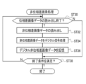
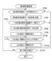
- FIG. 5 is a conceptual diagram showing an example of incident characteristics of subject light with respect to the first retardation pixel and the second retardation pixel included in the photoelectric conversion element shown in FIG.
- FIG. 5 is a schematic block diagram which shows an example of the structure of the non-phase difference pixel included in the photoelectric conversion element shown in FIG.
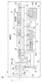
- It is a lock diagram which shows an example of the relationship between the control circuit included in the image pickup device which concerns on 1st Embodiment, and each peripheral device.
- CPU refers to the abbreviation of "Central Processing Unit”.
- GPU refers to the abbreviation of "Graphics Processing Unit”.
- RAM is an abbreviation for "Random Access Memory”.
- ROM is an abbreviation for "Read Only Memory”.
- DRAM refers to the abbreviation of "Dynamic Random Access Memory”.
- SRAM refers to the abbreviation of "Static Random Access Memory”.
- LSI refers to the abbreviation of "Large-Scale Integration”.
- ASIC refers to the abbreviation of "Application Special Integrated Circuit”.
- PLD refers to the abbreviation of "Programmable Logical Device”.
- FPGA refers to the abbreviation of "Field-Programmable Gate Array”.
- SSD refers to the abbreviation of "Solid State Drive”.
- USB refers to the abbreviation of "Universal Serial Bus”.
- HDD refers to the abbreviation of “Hard Disk Drive”.
- EEPROM refers to the abbreviation of "Electrically Erasable and Programmable Read Only Memory”.
- CCD refers to the abbreviation for "Charge Coupled Device”.
- CMOS is an abbreviation for "Complementary Metal Oxide Semiconducor”.
- EL refers to the abbreviation for "Electro-Luminescence”.
- a / D refers to the abbreviation of "Analog / Digital”.
- I / F refers to the abbreviation of "Interface”.
- UI refers to the abbreviation of "User Interface”.
- PC refers to the abbreviation of "Personal Computer”.
- AF refers to the abbreviation for "Auto-Focus”.
- AE refers to the abbreviation of "Automatic Exposure”.
- SoC refers to the abbreviation of "System-on-a-chip”.
- OIS refers to the abbreviation of "Optical Image Stabilization".
- BIS is an abbreviation for “Body Image Stabilization”.
- EIS is an abbreviation for "Electronic Image Stabilization”.
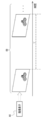
- the image pickup apparatus 10 is an interchangeable lens camera.
- the image pickup apparatus 10 includes an image pickup apparatus main body 12 and an interchangeable lens 14 that is interchangeably attached to the image pickup apparatus main body 12.
- the image pickup device main body 12 is provided with an image pickup element 44.
- the interchangeable lens 14 has an image pickup lens 40. When the interchangeable lens 14 is attached to the image pickup device main body 12, the subject light indicating the subject is transmitted through the image pickup lens 40 and imaged on the image pickup surface 44A of the image pickup device 44.
- a release button 20 and a dial 22 are provided on the upper surface of the image pickup apparatus main body 12.
- the dial 22 is operated when setting the operation mode of the imaging system, the operation mode of the reproduction system, and the like.
- the release button 20 functions as an imaging preparation instruction unit and an imaging instruction unit, and can detect a two-step pressing operation of an imaging preparation instruction state and an imaging instruction state.
- the imaging preparation instruction state refers to a state in which the image is pressed from the standby position to the intermediate position (hereinafter, referred to as "half-pressed position"), and the imaging instruction state is the final pressed position beyond the intermediate position (hereinafter, "half-pressed position"). It refers to the state in which it is pressed to the "fully pressed position").
- the "state of being pressed from the standby position to the half-pressed position” is referred to as the "half-pressed state”
- the “state of being pressed from the standby position to the fully-pressed position” is referred to as the "fully-pressed state”.
- the display moving image imaging mode and the recording imaging mode are selectively set as operation modes according to the user's instruction.
- the AF mode is set according to the user's instruction.
- the AE function is activated to set the exposure state for each frame, and the AF function is activated to control focusing, so that imaging for display moving images is performed. Will be done.
- a live view image is generated by performing imaging for a display moving image. In general, the live view image is also referred to as a through image.
- the imaging mode for recording is roughly divided into an imaging mode for moving image recording and an imaging mode for still image recording, and the imaging mode for moving image recording and the imaging mode for still image recording are selectively selected according to a user's instruction.
- Set In the image pickup apparatus 10, when the AF mode is set in the image pickup mode for moving image recording, the AE function is activated to set the exposure state for each frame, and the AF function is activated to control focusing and record. Imaging for moving images is performed.
- the moving image obtained by imaging for the recording moving image has a higher resolution than the live view image, and is a default storage device such as a memory card, a USB memory, an SSD, or an HDD (hereinafter, simply "default". It is stored in a storage device).
- the default storage device is an example of the "storage device" according to the technique of the present disclosure.
- the shooting conditions are adjusted by pressing the release button 20 halfway, and then when the release button 20 is continuously pressed fully, still image imaging is performed. It is said. That is, after the AE function works to set the exposure state by pressing the release button 20 halfway, the AF function works to control focusing, and when the release button 20 is fully pressed, it is for a recorded still image. Imaging is performed.
- the still image obtained by performing the imaging for the recorded still image is stored in the default storage device.
- the AF mode is roughly classified into a normal AF mode and a continuous AF mode, and the normal AF mode and the continuous AF mode are selectively set according to a user's instruction.
- the normal AF mode is an AF mode in which focusing control is performed with the focal position fixed during the half-pressed state.
- the continuous AF mode is an AF mode that continuously maintains the in-focus state for a specified subject without fixing the focal position during the half-pressed state.
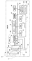
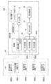
- the image pickup device 10 includes a computer 13, drivers 23, 26, communication I / F 25, signal processing circuit 30, vibration sensor 32, position detection sensor 39, storage device 42, external I / F 46, and the like. And a UI device 43.
- the computer 13 includes a CPU 35, a ROM 36, and a RAM 37, and the CPU 35, the ROM 36, and the RAM 37 are connected to each other via a bus line 38.
- drivers 23 and 26, communication I / F25, signal processing circuit 30, vibration sensor 32, position detection sensor 39, storage device 42, external I / F46, and UI device 43 are also connected to the bus line 38. ..
- the CPU 35 controls the entire imaging device 10. Various programs are stored in the ROM 36. The CPU 35 reads various programs from the ROM 36 and expands the read various programs into the RAM 37. The CPU 35 controls the entire image pickup apparatus 10 according to various programs developed in the RAM 37.
- the storage device 42 is a non-volatile storage device such as an SSD, HDD, or EEPROM.
- the CPU 35 reads and writes various information to and from the storage device 42.
- the external I / F46 is a communication device having an FPGA.
- a default storage device is connected to the external I / F 46.
- the CPU 35 reads and writes various information to and from the default storage device via the external I / F 46.
- an arithmetic unit such as a PC or a server is also connected to the external I / F46.
- the external I / F 46 controls the exchange of various information between the CPU 35 and the arithmetic unit.
- the UI device 43 is a device that receives instructions from the user and presents information to the user.
- the UI device 43 includes a reception device 43A and a display 43B.
- An example of the display 43B is a liquid crystal display.
- the display 43B may be not a liquid crystal display but another type of display such as an organic EL display.
- the display 43B displays character information as well as various images such as a live view image and a still image.
- the display 43B is an example of a "display device" according to the technique of the present disclosure.
- the CPU 35 is an example of a "control unit (control processor)" according to the technique of the present disclosure.
- the reception device 43A is provided with a hard key unit, a touch panel, and the like.
- the hard key section is a plurality of hard keys including a release button 20 (see FIG. 1) and a dial 22 (see FIG. 1).
- the touch panel is a transmissive touch panel and is superimposed on the surface of the display area of the display 43B. The touch panel detects contact with an indicator such as a finger or a stylus pen.
- the CPU 35 operates according to various instructions received by the reception device 43A.
- the vibration sensor 32 is a device including a gyro sensor, and detects the vibration given to the image pickup device 10.
- the vibration given to the image pickup device 10 includes, for example, vibration given to the image pickup device 10 by a user holding the image pickup device 10, and vibration due to wind to the image pickup device 10 installed on a support such as a tripod. , And vibration given by the vehicle.
- the gyro sensor detects the amount of rotation around each axis (see FIG. 1) of the pitch axis PA, the yaw axis YA, and the roll axis RA (the axis parallel to the optical axis L1).
- the vibration sensor 32 converts the amount of rotation around the pitch axis PA and the amount of rotation around the yaw axis YA detected by the gyro sensor into a amount of displacement in a two-dimensional plane parallel to the pitch axis PA and the yaw axis YA.
- the vibration of the image pickup apparatus 10 is detected.
- the vibration sensor 32 outputs vibration data indicating the detected vibration to the CPU 35.
- the meaning of parallelism in the first embodiment according to the technique of the present disclosure includes not only the meaning of perfect parallelism but also the meaning of substantially parallelism including errors allowed in design and manufacturing.
- the image pickup lens 40 includes an objective lens 15A and a lens group 15B.
- the image sensor 44 is located behind the image sensor 40.
- the objective lens 15A and the lens group 15B are arranged in the order of the objective lens 15A and the lens group 15B along the optical axis L1 from the subject side to the image sensor 44 side.
- the vibration sensor 32 has a built-in temperature sensor 34.
- the temperature sensor 34 measures the temperature inside the vibration sensor 32, and outputs temperature data indicating the measured temperature to the CPU 35.
- a communication I / F 25, a driver 26, and a signal processing circuit 30 are connected to the image sensor 44.
- the communication I / F 25 is a communication device having an FPGA, and controls the exchange of various signals between the CPU 35 and the image sensor 44.
- the driver 26 supplies a timing control signal to the image sensor 44 under the control of the CPU 35.
- the timing control signal refers to, for example, a vertical synchronization signal and a horizontal synchronization signal.
- the vertical synchronization signal is a signal that defines the timing at which imaging for one frame is started.
- the horizontal synchronization signal is a signal that defines the timing at which imaging for one horizontal line is started.
- the signal processing circuit 30 is a device including an ASIC.
- Image data 69 obtained by capturing an image of a subject by the image sensor 44 is input to the signal processing circuit 30.
- the image data 69 is data indicating an image of a subject.
- the signal processing circuit 30 performs various signal processing on the image data 69 input from the image sensor 44.
- Various signal processings include known signal processing such as white balance adjustment, sharpness adjustment, gamma correction, color space conversion processing, and color difference correction.
- the signal processing circuit 30 includes an ASIC and an FPGA. And / or the device may include a PLD.
- the signal processing circuit 30 may be a computer including a CPU, a ROM, and a RAM. The number of CPUs may be singular or plural. Further, the signal processing circuit 30 may be realized by a combination of a hardware configuration and a software configuration.
- the image pickup lens 40 includes an objective lens 15A and a lens group 15B.
- the objective lens 15A and the lens group 15B are arranged in the order of the objective lens 15A and the lens group 15B along the optical axis L1 from the subject side to the imaging surface 44A side.
- a movable diaphragm (not shown) and a mechanical shutter (not shown) are arranged between the lens group 15B and the image sensor 44.
- the diaphragm and the mechanical shutter are arranged in the order of the diaphragm and the mechanical shutter along the optical axis L1 from the lens group 15B side to the image sensor 44 side.
- the diaphragm operates by receiving power from a drive source (not shown) such as a motor, and the opening of the diaphragm is changed by operating the diaphragm, whereby the exposure is adjusted.
- the mechanical shutter operates by receiving power from a drive source (not shown) such as a motor.
- the subject light passes through the image pickup lens 40 and is imaged on the image pickup surface 44A via the mechanical shutter.
- the lens group 15B includes a focus lens 15B1, a zoom lens (not shown), and an anti-vibration lens 15B2.
- the focus lens 15B1, the zoom lens, and the anti-vibration lens 15B2 are the focus lens 15B1, the zoom lens, and the anti-vibration lens along the optical axis L1 from the objective lens 15A side to the image pickup element 44 side.
- the lenses 15B2 are arranged in this order.
- the focus lens 15B1 and the zoom lens move along the optical axis L1 according to the given power.
- the anti-vibration lens 15B2 fluctuates in the direction perpendicular to the optical axis of the anti-vibration lens 15B2.
- the meaning of "vertical" in the first embodiment according to the technique of the present disclosure includes not only the meaning of perfect vertical but also the meaning of substantially vertical including errors allowed in design and manufacturing. ..
- the focusing lens 15B1 moves along the optical axis L1 under the control of the CPU 35, so that the subject light is imaged on the imaging surface 44A at the focusing position according to the subject distance.
- the "focusing position” referred to here refers to the position of the focusing lens 15B1 on the optical axis L1 in the in-focus state.
- the control of aligning the focusing lens 15B1 with the in-focus position is referred to as "AF control".
- blurring occurs due to the vibration given to the image pickup apparatus 10 (hereinafter, also simply referred to as “vibration").
- “blurring” means a subject obtained by forming an image on the imaging surface 44A by tilting the optical axis L1 with respect to the reference axis due to vibration. Refers to a decrease in image fluctuation.
- the "reference axis” referred to here refers to, for example, the optical axis L1 in a state where no vibration is applied.
- Examples of the subject image include an optical image and an electronic image (image). The subject image changes as the positional relationship between the optical axis L1 and the imaging surface 44A changes.
- the image pickup device 10 is provided with an optical blur correction unit 29 in order to correct the deviation.
- the optical blur correction unit 29 is an example of a “correction unit” according to the technique of the present disclosure.
- the "correction unit” can be paraphrased as a “correction device”, a “correction mechanism”, an “optical correction device”, or an “optical correction mechanism”.
- the optical blur correction unit 29 operates under the control of the CPU 35 described later, and optically corrects the blur based on the vibration data output from the vibration sensor 32.
- "correction of blurring” includes not only the meaning of eliminating blurring but also the meaning of reducing blurring.
- the image obtained by capturing the subject by the imaging device 10 is optical to the extent that the blur caused by the vibration given to the imaging device 10 is not visually perceived.
- the description will be made on the premise that the blur is corrected by the blur correction unit 29.
- the optical blur correction unit 29 includes a vibration isolation lens 15B2, an actuator 17, a driver 23, and a position detection sensor 39.
- a method of correcting blur by the optical blur correction unit 29 various well-known methods can be adopted.
- OIS is adopted as a method of correcting blur.
- the OIS refers to a method of correcting blurring by moving the anti-vibration lens 15B2 based on vibration data obtained by detecting vibration by a vibration sensor 32 (described later). Specifically, the blur correction is performed by moving the anti-vibration lens 15B2 by the amount of the blur in the direction of canceling the blur.
- An actuator 17 is attached to the anti-vibration lens 15B2.
- the actuator 17 is a shift mechanism on which a coil motor is mounted, and by driving the coil motor, the anti-vibration lens 15B2 is changed in a direction perpendicular to the optical axis of the anti-vibration lens 15B2.
- a shift mechanism in which a coil motor is mounted is illustrated as the actuator 17, but the technique of the present disclosure is not limited to this, and instead of the coil motor, other stepping motors, piezo elements, or the like can be used.
- a power source may be applied.
- the actuator 17 is controlled by the driver 23.
- the position of the anti-vibration lens 15B2 mechanically fluctuates with respect to the optical axis L1.
- the position detection sensor 39 detects the current position of the anti-vibration lens 15B2 and outputs a position signal indicating the detected current position.
- a device including a Hall element is adopted as an example of the position detection sensor 39.
- the current position of the anti-vibration lens 15B2 refers to the current position in the two-dimensional plane of the anti-vibration lens.
- the anti-vibration lens two-dimensional plane refers to a two-dimensional plane perpendicular to the optical axis of the anti-vibration lens 15B2.
- a device including a Hall element is adopted as an example of the position detection sensor 39, but the technique of the present disclosure is not limited to this, and a magnetic sensor, a photo sensor, or the like is adopted instead of the Hall element. You may.
- the image sensor 44 is an example of a "stacked image sensor" according to the technique of the present disclosure.
- the image sensor 44 is a CMOS image sensor.
- the technique of the present disclosure is not limited to this, and for example, the technique of the present disclosure is established even if the image sensor 44 is a CCD image sensor. ..
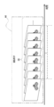
- the image pickup device 44 when the subject is imaged at the image pickup frame rate, as shown in FIG. 3A as an example, a plurality of image data 69 indicating each image of the subject is generated. Further, the image sensor 44 outputs a plurality of generated image data 69 at an output frame rate. Both the imaging frame rate and the output frame rate are variable frame rates.
- the imaging frame rate is an example of the "first frame rate” according to the technique of the present disclosure
- the output frame rate is an example of the "second frame rate" according to the technique of the present disclosure.
- the imaging frame rate and the output frame rate have a relationship of "imaging frame rate> output frame rate". That is, the imaging frame rate is a frame rate higher than the output frame rate, and is defined by a vertical synchronization signal which is one of the timing control signals.
- the imaging frame rate is a frame rate at which imaging for 8 frames is performed within the period T
- the output frame rate is a frame rate for 2 frames within the period T as shown in FIG. 3B. Is the frame rate at which the output of is performed.
- 240 fps frame per second
- 60 fps is mentioned as an example of the output frame rate.
- the image pickup element 44 has a photoelectric conversion element 61, a processing circuit 62, and a memory 64 built-in.
- the processing circuit 62 is an example of the “processor” according to the technique of the present disclosure
- the memory 64 is an example of the “storage unit (memory)” according to the technique of the present disclosure.
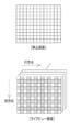
- the image sensor 44 is an image sensor in which the photoelectric conversion element 61, the processing circuit 62, and the memory 64 are integrated into one chip. That is, the photoelectric conversion element 61, the processing circuit 62, and the memory 64 are packaged in one package. In the image sensor 44, the processing circuit 62 and the memory 64 are laminated on the photoelectric conversion element 61.
- the photoelectric conversion element 61 and the processing circuit 62 are electrically connected to each other by a bump (not shown) having conductivity such as copper, and the processing circuit 62 and the memory 64 are also conductive such as copper. They are electrically connected to each other by bumps (not shown).
- a three-layer structure of a photoelectric conversion element 42, a processing circuit 110, and a memory 112 is illustrated, but the technique of the present disclosure is not limited to this, and a memory layer in which the processing circuit 110 and the memory 112 are one layer. And may have a two-layer structure of the photoelectric conversion element 42, or may be a two-layer structure of a processor layer having the processing circuit 110 and the photoelectric conversion element 42 as one layer and a memory 112. Further, the memory 112 may be built in the processing circuit 110.
- the processing circuit 62 is, for example, an LSI, and the memory 64 is, for example, a DRAM.
- the technique of the present disclosure is not limited to this, and SRAM may be adopted as the memory 64 instead of DRAM.
- the processing circuit 62 is a device including an ASIC and an FPGA, and controls the entire image sensor 44 according to the instruction of the CPU 35.
- the processing circuit 62 is realized by a device including an ASIC and an FPGA is given here, the technique of the present disclosure is not limited to this, and for example, the ASIC, FPGA, and / or PLD. It may be a device including.
- a computer including a CPU, a ROM, and a RAM may be adopted. The number of CPUs may be singular or plural.
- the processing circuit 62 may be realized by a combination of a hardware configuration and a software configuration.
- the photoelectric conversion element 61 has a plurality of photodiodes arranged in a matrix.
- An example of a plurality of photodiodes is a photodiode for "4896 x 3265" pixels.
- a color filter is arranged on each photodiode included in the photoelectric conversion element 61.
- the color filter includes a G filter corresponding to G (green), an R filter corresponding to R (red), and a B filter corresponding to B (blue), which contribute most to obtain a luminance signal.
- the photoelectric conversion element 61 has R pixels, G pixels, and B pixels (see FIG. 5).
- the R pixel is a pixel corresponding to the photodiode in which the R filter is arranged
- the G pixel is the pixel corresponding to the photodiode in which the G filter is arranged
- the B pixel is the photodiode in which the B filter is arranged. It is a pixel corresponding to.
- the image sensor 44 has a so-called electronic shutter function, and by activating the electronic shutter function under the control of the CPU 35, the charge accumulation time of each photodiode in the photoelectric conversion element 61 is controlled.
- the charge accumulation time refers to the so-called shutter speed.
- the image pickup for a still image and the image pickup for a moving image are performed by a rolling shutter method.
- the rolling shutter method is exemplified here, the technique of the present disclosure is not limited to this, and a global shutter method may be applied instead of the rolling shutter method.
- the processing circuit 62 reads out the image data 69 obtained by capturing the image of the subject by the photoelectric conversion element 61.
- the image data 69 is a signal charge stored in the photoelectric conversion element 61.
- the processing circuit 62 performs A / D conversion on the analog image data 69 read from the photoelectric conversion element 61.
- the processing circuit 62 stores the digital image data 69 obtained by performing A / D conversion on the analog image data 69 in the memory 64.
- the memory 64 includes a plurality of storage areas, and in each of the plurality of storage areas, for example, digital image data 69 is stored in pixel units at addresses corresponding to the pixels of the photoelectric conversion element 61 for each frame. To. Further, the processing circuit 62 randomly accesses the plurality of storage areas.
- the processing circuit 62 is connected to the CPU 35 and the signal processing circuit 30.
- the processing circuit 62 sends and receives various signals to and from the CPU 35. Further, the processing circuit 62 outputs the digital image data 69 to the signal processing circuit 30.
- the R pixel, the G pixel, and the B pixel have predetermined periodicity in each of the row direction (horizontal direction) and the column direction (vertical direction). It is arranged in.
- the R pixel, the G pixel, and the B pixel are arranged in a periodicity corresponding to the X-Trans (registered trademark) arrangement.
- X-Trans registered trademark
- FIG. 5 an X-Trans array is illustrated, but the technique of the present disclosure is not limited to this, and the array of R pixel, G pixel, and B pixel is a Bayer array, a honeycomb array, or the like. It may be.
- R pixels, G pixels, and B pixels are arranged in the row direction in the order of G pixel, B pixel, R pixel, G pixel, R pixel, and B pixel.
- the R pixel, the G pixel, and the B pixel are circulated and arranged in the row direction in the order of the R pixel, the G pixel, the G pixel, the B pixel, the G pixel, and the G pixel.
- the R pixel, the G pixel, and the B pixel are circulated and arranged in the row direction in the order of the B pixel, the G pixel, the G pixel, the R pixel, the G pixel, and the G pixel.
- the R pixel, the G pixel, and the B pixel are circulated and arranged in the row direction in the order of the G pixel, the R pixel, the B pixel, the G pixel, the B pixel, and the R pixel.
- the R pixel, the G pixel, and the B pixel are circulated and arranged in the row direction in the order of the B pixel, the G pixel, the G pixel, the R pixel, the G pixel, and the G pixel.
- the R pixel, the G pixel, and the B pixel are circulated and arranged in the row direction in the order of the R pixel, the G pixel, the G pixel, the B pixel, the G pixel, and the G pixel.
- the arrangement pattern of the R pixels, G pixels, and B pixels in the first to sixth rows is repeated in the column direction in units of 6 rows, so that the entire R pixels, G pixels, and B pixels of the photoelectric conversion element 61 are repeated.
- the arrangement pattern of is formed.
- the photoelectric conversion element 61 is formed to include a group of photosensitive pixels.
- the photosensitive pixel group has two types of photosensitive pixels, a phase difference pixel and a non-phase difference pixel N which is a pixel different from the phase difference pixel.
- the non-phase difference pixel N is also referred to as a normal pixel.
- a plurality of retardation pixel lines 61A and a plurality of non-phase difference pixel lines 61B are arranged on the imaging surface 44A.
- the retardation pixel line 61A is a horizontal line including a retardation pixel.
- the phase difference pixel line 61A is a horizontal line in which phase difference pixels and non-phase difference pixels N are mixed.
- the non-phase difference pixel line 61B is a horizontal line including only a plurality of non-phase difference pixels N, that is, a horizontal line composed of a plurality of non-phase difference pixels N.
- the retardation pixel lines 61A and the non-phase difference pixel lines 61B corresponding to the predetermined number of lines are alternately arranged along the column direction.
- the "default number of lines" referred to here refers to, for example, two lines.
- 2 lines are illustrated as the default number of lines, but the technique of the present disclosure is not limited to this, and the default number of lines may be 3 or more lines, or more than 10 lines. , Dozens of lines, hundreds of lines, and the like.
- the phase difference pixel line 61A is arranged by skipping two rows in the column direction from the first row to the last row. Some pixels of the phase difference pixel line 61A are phase difference pixels. Specifically, the phase difference pixel line 61A is a horizontal line in which phase difference pixels and non-phase difference pixels N are periodically arranged. The phase difference pixel is roughly classified into a first phase difference pixel L and a second phase difference pixel R. In the phase difference pixel line 61A, the first phase difference pixel L and the second phase difference pixel R are alternately arranged as G pixels at intervals of several pixels in the line direction.
- the first phase difference pixel L and the second phase difference pixel R are arranged so as to appear alternately in the column direction.
- the first phase difference pixel L, the second phase difference pixel R, the first phase difference pixel L, and the second phase difference pixel R are arranged along the column direction from the first row. They are arranged in order. That is, the first phase difference pixel L and the second phase difference pixel R are alternately arranged along the column direction from the first row.
- the second phase difference pixel R, the first phase difference pixel L, the second phase difference pixel R, and the first phase difference pixel along the column direction from the first row are arranged in the order of L. That is, the second phase difference pixel R and the first phase difference pixel L are alternately arranged along the column direction from the first row.
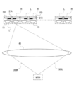
- the first retardation pixel L includes a microlens 19, a light-shielding member 21A, and a photodiode PD.
- a light-shielding member 21A is arranged between the microlens 19 and the light-receiving surface of the photodiode PD.
- the left half of the light receiving surface of the photodiode PD in the row direction (the left side when facing the subject from the light receiving surface (in other words, the right side when facing the light receiving surface from the subject)) is shielded by the light shielding member 21A.
- the second phase difference pixel R includes a microlens 19, a light-shielding member 21B, and a photodiode PD.
- a light-shielding member 21B is arranged between the microlens 19 and the light receiving surface of the photodiode PD.
- the right half of the light receiving surface of the photodiode PD in the row direction (the right side when facing the subject from the light receiving surface (in other words, the left side when facing the light receiving surface from the subject)) is shielded by the light shielding member 21B.
- the luminous flux passing through the exit pupil of the image pickup lens 40 is roughly classified into left region passing light 300L and right region passing light 300R.
- the left region passing light 300L refers to the left half of the luminous flux passing through the ejection pupil of the imaging lens 40 when facing the subject side from the phase difference pixel side
- the right region passing light 300R refers to the imaging lens 40.
- the luminous flux passing through the ejection pupil of the above it refers to the luminous flux of the right half when facing the subject side from the phase difference pixel side.
- the luminous flux passing through the exit pupil of the image pickup lens 40 is divided into left and right by the microlens 19 functioning as a pupil dividing portion and the light-shielding members 21A and 21B, and the first phase difference pixel L receives the left region passing light 300L as the subject light. Then, the second phase difference pixel R receives the right region passing light 300R as the subject light. As a result, the first phase difference image data showing the first phase difference image corresponding to the subject image corresponding to the left region passing light 300L and the second phase difference image corresponding to the subject image corresponding to the right region passing light 300R are obtained.
- the second phase difference image data shown is generated by the image pickup device 44.
- phase difference pixels when it is not necessary to distinguish between the first phase difference pixel L and the second phase difference pixel R, they are referred to as "phase difference pixels”. Further, in the following, for convenience of explanation, when it is not necessary to separately explain the light-shielding members 21A and 21B, they are referred to as “light-shielding members” without reference numerals. When it is not necessary to distinguish between the first phase difference image data and the second phase difference image data, it is referred to as "phase difference image data”.
- the non-phase difference pixel is different from the phase difference pixel in that it does not have a light-shielding member.
- the photodiode PD of the non-phase difference pixel receives the left region passing light 300L and the right region passing light 300R as the subject light.
- the image sensor 44 generates non-phase difference image data showing the non-phase difference image corresponding to the subject light.
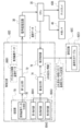
- the processing circuit 62 includes a reading circuit 62A, a digital processing circuit 62B, a storage circuit 62C, and a control circuit 62D.
- the read circuit 62A includes a first read circuit 62A1 and a second read circuit 62A2. Each of the first read circuit 62A1 and the second read circuit 62A2 is connected to the photoelectric conversion element 61, the digital processing circuit 62B, and the control circuit 62D. Each of the digital processing circuit 62B, the storage circuit 62C, and the memory 64 is connected to the control circuit 62D. The control circuit 62D is connected to the signal processing circuit 30 and the CPU 35.
- image data 69 is roughly classified into analog image data 69A and digital image data 69B.
- image data 69 when it is not necessary to distinguish between the analog image data 69A and the digital image data 69B, it is referred to as "image data 69".
- the analog image data 69A includes analog phase difference image data 69A1 which is analog phase difference image data related to the phase difference pixel and analog non-phase difference image data 69A2 which is analog non-phase difference image data related to the non-phase difference pixel N. It is roughly divided.
- the digital image data 69B is roughly classified into digital phase difference image data 69B1 and digital non-phase difference image data 69B2.
- the digital phase difference image data 69B1 is image data obtained by digitizing the analog phase difference image data 69A1.
- the digital non-phase difference image data 69B2 is image data obtained by digitizing the analog non-phase difference image data 69A2.
- the analog image data 69A and the digital image data 69B are examples of "image data" according to the technique of the present disclosure.
- the control circuit 62D is supplied with various signals such as temperature data, position signal, and vibration data from the CPU 35 to the control circuit 62D. Further, a timing control signal is supplied to the control circuit 62D from the driver 26 (see FIG. 2).
- the reading circuit 62A reads out the analog image data 69A obtained by capturing the subject at the imaging frame rate in units of horizontal lines. That is, the reading circuit 62A controls the photoelectric conversion element 61 under the control of the control circuit 62D, and reads the analog image data 69A from the photoelectric conversion element 61 in units of horizontal lines.
- the imaging frame rate is defined by a vertical synchronization signal which is one of the timing control signals supplied from the driver 26 (see FIG. 2), and the read timing in units of horizontal lines is horizontal synchronization which is one of the timing control signals. Determined according to the signal.
- the read circuit 62A is a circuit that can selectively read the analog phase difference image data 69A1 and the analog non-phase difference image data 69A2 for all the pixels included in the photoelectric conversion element 61. As will be described in detail later, the selective reading of the analog phase difference image data 69A1 and the analog non-phase difference image data 69A2 is realized by the first read circuit 62A1 and the second read circuit 62A2.
- analog phase difference image data 69A1 and the analog non-phase difference image data 69A2 are selectively read out for all the pixels included in the photoelectric conversion element 61 , but the technique of the present disclosure is described. Not limited to this.
- the analog phase difference image data 69A1 and the analog non-phase difference image data 69A2 may be selectively read out for a designated part of all the pixels included in the photoelectric conversion element 61. ..
- a vertical synchronization signal is supplied to the control circuit 62D from the driver 26 (see FIG. 2), and the control circuit 62D transfers the vertical synchronization signal to the reading circuit 62A.
- the read circuit 62A starts reading one frame of analog image data 69A to the photoelectric conversion element 61.
- the control circuit 62D transfers the vertical synchronization signal supplied from the driver 26 (see FIG. 2) to the first read circuit 62A1 and the second read circuit 62A2.
- the analog phase difference image data 69A1 is read from the phase difference pixel and the analog non-phase difference image data is read from the non-phase difference pixel N.
- the reading of 69A2 is performed independently.
- the reading of the analog phase difference image data 69A1 is performed by the first reading circuit 62A1, and the reading of the analog non-phase difference image data 69A2 is performed by the second reading circuit 62A2.
- the first read circuit 62A1 starts reading the analog phase difference image data 69A1 for one frame to the photoelectric conversion element 61. Then, the first read circuit 62A1 reads the analog phase difference image data 69A1 from each of the phase difference pixels for each phase difference pixel line 61A according to the horizontal synchronization signal input from the control circuit 62D. When the read start condition (described later) is satisfied, the second read circuit 62A2 starts reading one frame of analog non-phase difference image data 69A2 to the photoelectric conversion element 61.
- the second read circuit 62A2 reads the analog non-phase difference image data 69A2 from each of the non-phase difference pixels N for each non-phase difference pixel line 61B according to the horizontal synchronization signal input from the control circuit 62D.
- the "reading start condition" referred to here means that the vertical synchronization signal is input from the control circuit 62D, and the reading of the analog phase difference image data 69A1 for one frame by the first reading circuit 62A1 is completed. Refers to a condition.
- the reading circuit 62A performs analog signal processing on the analog image data 69A read from the photoelectric conversion element 61.
- the analog signal processing includes known processing such as noise canceling processing and analog gain processing.
- the noise canceling process is a process for canceling noise caused by variations in characteristics between pixels included in the photoelectric conversion element 61.
- the analog gain process is a process of applying a gain to the analog image data 69A.
- the analog image data 69A subjected to the analog signal processing in this way is output to the digital processing circuit 62B by the reading circuit 62A.
- the digital processing circuit 62B includes an A / D converter 62B1.
- the digital processing circuit 62B performs digital signal processing on the analog image data 69A input from the reading circuit 62A.
- Digital signal processing includes, for example, correlated double sampling, A / D conversion by the A / D converter 62B1, and digital gain processing.
- Correlated double sampling is performed on the analog image data 69A by the digital processing circuit 62B.
- the analog image data 69A subjected to the signal processing of the correlated double sampling is subjected to A / D conversion by the A / D converter 62B1, whereby the analog image data 69A is digitized and the digital image data. 69B is obtained.
- the digital image data 69B is subjected to digital gain processing by the digital processing circuit 62B.
- the digital gain process refers to a process of applying a gain to the digital image data 69B.
- the control circuit 62D acquires the digital image data 69B obtained by performing the digital signal processing from the digital processing circuit 62B, and stores the acquired digital image data 69B in the memory 64.
- the memory 64 is a memory capable of storing a plurality of frames of digital image data 69B.
- the memory 64 has a plurality of storage areas, and the digital image data 69B is stored in the corresponding storage area of the memory 64 in pixel units by the control circuit 62D.
- the control circuit 62D has random access to the memory 64, and acquires digital non-phase difference image data 69B2 from the memory 64.
- the control circuit 62D performs signal processing on the digital non-phase difference image data 69B2 acquired from the memory 64. Examples of the "signal processing" referred to here include simultaneous processing, digital thinning processing, digital addition processing, and data embedding processing.
- the simultaneous processing is a process of calculating all color information for each pixel from a mosaic image corresponding to an array of color filters. For example, in the case of an image sensor composed of RGB three-color color filters, all RGB color information is calculated for each pixel from a mosaic image composed of RGB.
- the digital thinning process is a process of thinning out the pixels included in the digital non-phase difference image data 69B2 in line units.
- the line unit refers to, for example, a horizontal line unit and / or a vertical line unit.
- the digital addition process is, for example, a process of adding and averaging pixel values for a plurality of pixels included in the digital non-phase difference image data 69B2.
- Examples of the data embedding process include a process of embedding specific data in the lower empty bits of the digital non-phase difference image data 69B2.
- Examples of the "specific data" here include information that can specify the method of digital thinning processing performed on the digital non-phase difference image data 69B2, frame numbers that can specify frames, and the like.
- the control circuit 62D outputs the digital phase difference image data 69B1 and the practical image data (described later) which is the image-processed digital non-phase difference image data 69B2 to the signal processing circuit 30 at the output frame rate.
- the digital phase difference image data 69B1 is transferred to the CPU 35 via the signal processing circuit 30.
- the CPU 35 performs AF control based on the digital phase difference image data 69B1.
- Practical image data is also transferred to the CPU 35 via the signal processing circuit 30.
- the CPU 35 executes various processes on the practical image data.
- the various processes refer to, for example, a process of displaying an image indicated by the practical image data on the display 43B, a process of storing the practical image data in a default storage device, and the like.
- the storage circuit 62C stores the reference output table 62C1 (see FIG. 11).
- the reference output table 62C1 is a table in which the temperature of the vibration sensor 32 and the reference output level of the vibration sensor 32 (hereinafter, simply referred to as “reference output level”) are associated with each other.
- the unit of temperature is "° C”
- the unit of the output level of the vibration sensor 32 is "mdps”. ".
- the reference output level refers to the output level of the vibration sensor 32 in the state without vibration.
- the no-vibration state refers to a state in which the vibration sensor 32 is stationary, that is, a state in which vibration is not applied to the image pickup apparatus 10.
- a state in which the vibration sensor 32 is moving that is, a state in which vibration is applied to the image pickup apparatus 10
- the notation of the unit regarding the output level of the vibration sensor 32 will be omitted.
- the control circuit 62D is a position indicating signal based on the reference output level of the reference output table 62C1 stored in the storage circuit 62C and the temperature data, the position signal, and the vibration data supplied from the CPU 35. To generate. Then, the control circuit 62D outputs the generated position instruction signal to the CPU 35.
- the position indicating signal refers to a signal instructing the position of the anti-vibration lens 15B2 (see FIG. 2) in the above-mentioned anti-vibration lens two-dimensional plane.
- the CPU 35 controls the optical blur correction unit 29 according to the position indicating signal input from the control circuit 62D.
- the optical blur correction unit 29 corrects the blur by adjusting the position of the anti-vibration lens 15B2 to the position designated by the position indicating signal.
- a correction amount required for blur correction (hereinafter referred to as “blurring correction amount”) is calculated, and a position indicating signal is determined according to the calculated blur correction amount.
- the time integral value of the difference between the reference output level and the current output level of the vibration sensor 32 (hereinafter referred to as “current output level”) (in the example shown in FIG. 9, the shaded area). Area) corresponds to the amount of blur correction.
- the current output level matches the reference output level, but in the vibrating state, the current output level is higher or lower than the reference output level.
- the reference output level is constant as shown in the example shown in FIG. 9, but in reality, as shown in FIG. 10 as an example.
- the reference output level is not constant and is displaced.
- causes of displacement of the reference output level include the environment in which the vibration sensor 32 is installed and deterioration over time.
- the displacement of the reference output level is calculated as a time integral value, so that the error of the displacement of the reference output level is included in the blur correction amount.
- a blur correction amount larger than the actually required blur correction amount is calculated.
- the blur correction amount is a value other than "0", so that the optical blur correction unit 29 operates as if there is blur, even though it is not necessary to correct the blur. It ends up.
- the reference output level of the reference output table 62C1 is optimized, and the blur correction amount is calculated based on the optimized reference output level. Since the reference output level is different for each temperature of the vibration sensor 32, the reference output table 62C1 has a plurality of temperatures of the vibration sensor 32 and a reference output level, and different reference outputs are provided for each of the plurality of temperatures. The levels are associated in advance.
- a plurality of temperatures are defined in the range of 20.0 ° C to 27.0 ° C in 0.5 ° C increments.
- the temperature and the reference output level associated with each other are both fixed values.
- the modified reference output level is the reference output level after displacement in a state where the blur is corrected by the optical blur correction unit 29.
- the change reference output level is associated with each temperature in the range of 23.0 ° C to 26.0 ° C.
- the usage reference output level is used in the calculation of the time integral value, that is, the calculation of the blur correction amount. If the modified reference output level has not yet been obtained from the vibration sensor 32, the reference output level is adopted as the usage reference output level, and if the modified reference output level is obtained from the vibration sensor 32, the modified reference output level is used as the usage reference. Adopted as an output level.
- the reference output level is used as the reference output level for each temperature in the range of 20.0 ° C. to 22.5 ° C. and the range of 26.5 ° C. to 27.0 ° C. Has been adopted. Further, in the example shown in FIG. 11, a changed reference output level is adopted as the usage reference output level for each temperature in the range of 23.0 ° C to 26.0 ° C.
- the digital phase difference image data is obtained for each frame.
- 69B1 are associated in chronological order. That is, the digital phase difference image data 69B1 and the digital non-phase difference image data 69B2 are acquired by the control circuit 62D in units of one frame.
- the control circuit 62D when the control circuit 62D generates time-series data based on the time-series digital non-phase difference image data 69B2 obtained by imaging at the imaging frame rate, when the time-series data is generated.
- the series data is stored in the memory 64 by the FIFO method.
- the time series data is roughly classified into first frame data related to some frames and second frame data related to the remaining frames.
- the second frame data is frame data indicating a plurality of frames.
- the first frame data is image data 69B2a for signal processing.
- the signal processing image data 69B2a is the digital non-phase difference image data 69B2 itself, and the digital phase difference image data 69B1 in the same frame is associated with the digital non-phase difference image data 69B2 itself.
- the second frame data is the image data 69B2b for the first analysis, the image data 69B2c for the second analysis, and the image data 69B2d for the third analysis.
- each of the first analysis image data 69B2b, the second analysis image data 69B2c, and the third analysis image data 69B2d has a digital non-phase difference of one frame due to all the pixels of the imaging surface 44A.
- This is partial image data showing a part of the image data 69B2.
- the "partial image data indicating a part of the image” referred to here refers to, for example, a part of the image of the subject within the angle of view of the image pickup apparatus 10.
- Periodically defined frames in the time series data are frames defined at time intervals specified at 60 fps. That is, the time interval between the frames defined periodically is the time interval corresponding to the cycle defined by 60 fps.
- the term "between frames” as used herein means, for example, between temporally adjacent signal processing image data 69B2a, temporally adjacent first analysis image data 69B2b, and temporally adjacent second analysis image data. It refers to the space between 69B2c and the time-adjacent image data for third analysis 69B2d.
- Each of the signal processing image data 69B2a, the first analysis image data 69B2b, the second analysis image data 69B2c, and the third analysis image data 69B2d is obtained at a time interval specified by 60 fps and is stored in the memory 64. It is memorized by the method.
- Nth analysis image data is an image for the first analysis which is an image shown by the image data 69B2b for the first analysis
- an image for the second analysis which is an image shown by the image data 69B2c for the second analysis
- a second image is an image for the third image for analysis.
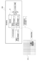
- the imaging surface 44A has an AF control target region 61C, which is an image side region to be AF controlled.
- the AF control target area 61C corresponds to a part of the object-side area of the subject that is designated as the target of AF control and is followed in the continuous AF mode.
- the AF control target area 61C may be an area designated according to an instruction received by the reception device 43A (see FIG. 2), or may be an area specified as a face area by a so-called face detection function.
- the Nth analysis image data is the digital non-phase difference corresponding to the in-focus state region of the digital non-phase difference image data 69B2 obtained by reading the analog non-phase difference image data 69A2 by the first read circuit 62A1.
- the in-focus region is an example of the "in-focus region" according to the technique of the present disclosure.
- the in-focus state region is an image-side region of the photosensitive pixel group in the AF control target region 61C that is in the in-focus state, that is, the in-focus state is continuously maintained under the continuous AF mode. Refers to the image side area.
- the in-focus state region is specified by analyzing the digital phase difference image data 69B1 obtained in the same frame as the digital non-phase difference image data 69B2 by the control circuit 62D.
- the control circuit 62D includes a processing unit 70, a first output unit 72, a second output unit 74, and a correction control unit 76.
- the processing unit 70 is an example of the “processing unit (processing circuit)" according to the technology of the present disclosure
- the first output unit 72 is the “first output unit (first output circuit)" of the technology of the present disclosure.
- the second output unit 74 is an example of the "second output unit” according to the technique of the present disclosure
- the correction control unit 76 is the "correction control unit (correction control circuit)" according to the technology of the present disclosure. This is an example.
- the processing unit 70 processes the image data 69.
- the processing unit 70 includes a practical image data generation unit 78, a first analysis unit 80A1, a second analysis unit 80A2, and a third analysis unit 80A3.
- the practical image data generation unit 78 is connected to the first output unit 72.
- the first analysis unit 80A1, the second analysis unit 80A2, and the third analysis unit 80A3 are connected to the second output unit 74.
- the second output unit 74 is connected to the correction control unit 76.
- the term "Nth analysis unit 80A" is used.
- the practical image data generation unit 78 acquires the signal processing image data 69B2a and the digital phase difference image data 69B1 associated with the signal processing image data 69B2a from the memory 64.
- the practical image data generation unit 78 generates practical image data by performing signal processing on the signal processing image data 69B2a acquired from the memory 64.
- the practical image data refers to, for example, still image data indicating a still image or live view image data indicating a live view image.
- the still image data and the live view image data are selectively switched according to the instruction received by the reception device 43A.
- still image data and live view image data are adopted as practical image data, but the technology of the present disclosure is not limited to this, and the practical image data is recording moving image data indicating a recording moving image. It may be.
- the first output unit 72 acquires the practical image data generated by the practical image data generation unit 78 and the digital phase difference image data 69B1 corresponding to the practical image data, and the acquired practical image data and digital phase difference image data. 69B1 is output at the output frame rate.
- the Nth analysis unit 80A acquires the Nth analysis image data from the memory 64, and derives the blur degree information by using the acquired Nth analysis image data.
- the blur degree information refers to information indicating the degree of blur included in the Nth analysis image, which is an image indicated by the Nth analysis image data.
- the degree of blurring is an index showing the effect of blurring correction by the optical blur correction unit 29.
- the first analysis unit 80A1 acquires the first analysis image data 69B2b and the digital phase difference image data 69B1 corresponding to the first analysis image data from the memory 64. As will be described in detail later, the first analysis unit 80A1 derives blurring degree information by analyzing the first analysis image data 69B2b and the digital phase difference image data 69B1 acquired from the memory 64.
- the blur degree information derived by the first analysis unit 80A1 is information indicating the degree of blur included in the first analysis image.
- the blur degree information derived by the first analysis unit 80A1 corresponds to the deviation amount of the reference output level, and corresponds to, for example, the blur amount remaining in the first analysis image without being corrected by the optical blur correction unit 29. It is expressed by the number of pixels to be used.
- the second analysis unit 80A2 acquires the second analysis image data 69B2c and the digital phase difference image data 69B1 corresponding to the second analysis image data from the memory 64. As will be described in detail later, the second analysis unit 80A2 derives blurring degree information by analyzing the second analysis image data 69B2c and the digital phase difference image data 69B1 acquired from the memory 64.
- the blur degree information derived by the second analysis unit 80A2 is information indicating the degree of blur included in the second analysis image.
- the blur degree information derived by the second analysis unit 80A2 corresponds to the deviation amount of the reference output level, for example, the blur amount remaining in the second analysis image without being corrected by the optical blur correction unit 29. It is expressed by the number of pixels to be used.
- the third analysis unit 80A3 acquires the third analysis image data 69B2d and the digital phase difference image data 69B1 corresponding to the third analysis image data from the memory 64. As will be described in detail later, the third analysis unit 80A3 derives blurring degree information by analyzing the third analysis image data 69B2d and the digital phase difference image data 69B1 acquired from the memory 64.
- the blur degree information derived by the third analysis unit 80A3 is information indicating the degree of blur included in the third analysis image.
- the blur degree information derived by the third analysis unit 80A3 corresponds to the deviation amount of the reference output level, for example, the blur amount remaining in the third analysis image without being corrected by the optical blur correction unit 29. It is expressed by the number of pixels to be used.
- the second output unit 74 acquires the blur degree information derived by the N analysis unit 80A from the N analysis unit 80A, and outputs the acquired blur degree information to the correction control unit 76 at the same rate as the output frame rate.
- a still image is a maximum resolution, that is, a full resolution image
- a live view image is an image having a lower resolution than a still image.
- the pixels are not thinned out, whereas in the live view image, the pixels are periodically thinned out in each of the row direction and the column direction.
- the Nth analysis unit 80A acquires the latest Nth analysis image data from the memory 64.
- the Nth analysis image data acquired from the memory 64 is partial image data having the highest resolution (full resolution) of the digital non-phase difference image data 69B2 for one frame.
- the partial image data refers to the digital non-phase difference image data 69B2 corresponding to the in-focus state region in the AF control target area 61C among the digital non-phase difference image data 69B2 for one frame.
- the Nth analysis unit 80A has a storage area 81.
- the Nth analysis image data acquired from the memory 64 is stored in the FIFO method, and a pair of temporally adjacent Nth analysis image data (hereinafter, simply “a pair of Nth analysis images"). (Also called “data”) is stored. That is, every time the Nth analysis image data is acquired from the memory 64 by the Nth analysis unit 80A, the acquired Nth analysis image data is stored in the storage area 81 by the FIFA method, and the previous time in the storage area 81 is stored. The Nth analysis image data and the latest Nth analysis image data are updated.
- the Nth analysis unit 80A compares a pair of Nth analysis image data in the storage area 81 each time the stored contents in the storage area 81 are updated, and derives blurring degree information from the comparison result. That is, the Nth analysis unit 80A identifies the number of pixels corresponding to the amount of blur remaining in the latest Nth analysis image data by comparing the pair of Nth analysis image data in the storage area 81. , The specified number of pixels is determined as blurring degree information.
- the second output unit 74 acquires blurring degree information from the Nth analysis unit 80A, and outputs the acquired blurring degree information to the correction control unit 76 at the same rate as the output frame rate.
- the first output unit 72 acquires the practical image data and the digital phase difference image data 69B1 for each frame from the practical image data generation unit 78, and outputs the acquired practical image data and the digital phase difference image data 69B1 at the output frame rate. Output to the signal processing circuit 30.
- the practical image data is output to the CPU 35 together with the digital phase difference image data 69B1 by the signal processing circuit 30.
- the CPU 35 performs continuous AF control according to the digital phase difference image data 69B1 input from the signal processing circuit 30. Further, the CPU 35 performs various processes based on the practical image data input from the signal processing circuit 30. For example, if the practical image data is still image data, the CPU 35 stores the still image data in a default storage device via an external I / F 46, or displays the still image on the display 43B. Further, if the practical image data is the live view image data, the CPU 35 causes the display 43B to display the live view image.
- the correction control unit 76 controls the optical blur correction unit 29 to correct the blur by using the vibration data and the usage reference output level in the reference output table 62C1.
- the correction control unit 76 updates the reference output table 62C1.
- the correction control unit 76 acquires temperature data and blur degree information. That is, the correction control unit 76 acquires the temperature data from the CPU 35 and the blur degree information from the second output unit 74. Then, the correction control unit 76 determines whether or not the reference output table 62C1 (see FIG. 11) needs to be updated based on the temperature data and the degree of blur information, and when it determines that the update is necessary, the reference output table 62C1 To update.
- the correction control unit 76 acquires the reference output level corresponding to the temperature indicated by the temperature data from the reference output table 62C1.
- the correction control unit 76 indicates by the temperature data by using a linear interpolation method (for example, an interpolation method).
- a linear interpolation method for example, an interpolation method.
- the reference output level when the temperature that does not exist in the reference output table 62C1 (hereinafter referred to as “absence temperature”) is 23.25 ° C. is the default temperature and the reference output level for the default temperature. Therefore, "506.2" is calculated by the linear interpolation method.
- the "existing temperature” referred to here refers to the temperature defined in the reference output table 62C1.
- 23.0 ° C. and 23.5 ° C. are shown as the default temperatures, and the reference output level “506” for 23.0 ° C. is used as the reference output level for the default temperature.
- a reference output level of "507" for 23.5 ° C. is shown.
- the correction control unit 76 calculates the change reference output level based on the reference output level acquired from the reference output table 62C1, the blur degree information acquired from the second output unit 74, and the temperature indicated by the temperature data. To do.
- the change reference output level is calculated by using, for example, a default arithmetic expression in which the reference output level, the degree of blurring information, the temperature, and the change reference output level limit value are set as independent variables, and the change reference output level is set as the dependent variable. Will be done.
- the change reference output level limit value refers to a value that limits the amount of change in the reference output level within the number of thinned pixels (described later).
- the number of pixels corresponding to the difference between the reference output level and the calculated change reference output level (hereinafter, also referred to as “output level difference”) (hereinafter, also referred to as “difference equivalent pixel number”) is the highest resolution image.
- the number of pixels of the live view image exceeds the number of thinned pixels (hereinafter, also simply referred to as “the number of thinned pixels”) with respect to the number of pixels, after the blur is corrected, the number of pixels corresponding to the difference is less than or equal to the number of thinned pixels. Even if there is, there is an increased possibility that blurring corresponding to the output level difference is visually perceived in an image such as a live view image.
- the output level difference appears as an increase or decrease in the angular velocity of the gyro sensor included in the vibration sensor 32, the displayed image is shifted by the increase or decrease in the angular velocity. How many pixels the image shifts due to the reference output level input from the vibration sensor 32 is determined by the number of pixels of the optical system such as the objective lens 15A and the lens group 15B included in the image pickup lens 40 (hereinafter, simply referred to as "optical system"). ).
- number of thinned pixels is an example of “degree of reduction in the number of pixels of image data” according to the technique of the present disclosure.
- thinning out is illustrated here as an example of reducing the number of pixels, the number of pixels may be reduced by a method other than thinning out, such as integration of pixels.
- the correction control unit 76 determines whether or not the reference output table 62C1 needs to be updated according to the calculated change reference output level.
- the correction control unit 76 updates the reference output table 62C1 when it determines that the reference output table 62C1 needs to be updated.
- the update of the reference output table 62C1 refers to the addition of a new change reference output level and the change of the existing change reference output level.
- the new addition of the changed reference output level refers to the new addition of the changed reference output level to the reference output table 62C1 when the changed reference output level is not determined for a certain temperature.
- the change reference output level in the range of 20.0 ° C. to 22.5 ° C. and the range of 26.5 ° C. to 27.0 ° C. is not determined, the temperature in this range is changed.
- a new calculated change reference output level is added.
- Changing the existing change reference output level refers to the change of the change reference output level that has already been decided for a certain temperature.
- the change reference output level in the range of 23.0 ° C to 26.0 ° C is determined.
- the change reference output level is calculated for temperatures in this range, and the existing change reference output level is calculated when the calculated new change reference output level is different from the existing change reference output level in the reference output table 62C1.
- New change The standard output level is changed.
- the change reference output level calculated by the correction control unit 76 for a temperature of 23.0 ° C. is “510”, it is not necessary to change the change reference output level.
- the change reference output level calculated by the correction control unit 76 for the temperature of 23.0 ° C. is a value other than "510”
- the change reference output level for the temperature of 23.0 ° C. is set by the correction control unit 76. It will be changed to the latest calculated value.
- the usage reference output level for the temperature of 23.0 ° C. is also changed to the same value as the changed reference output level after the update.
- the change reference output level for other temperatures is also determined in the reference output table 62C1, the change reference output level for other temperatures is also changed by using the linear interpolation method.
- the change reference output level for the existing temperature in the reference output table 62C1 is also changed.
- the change reference output level in the reference output table 62C1 is changed by the linear interpolation method with reference to the absence temperature and the change reference output level calculated for the absence temperature.
- the change reference output level of 23.0 ° C. is changed as the change reference output level of the absent temperature of 23.25 ° C. is changed from “510.8” to “512”.
- “510” is changed to "511.2”
- the change reference output level "511" at 23.5 ° C. is changed to "512.8".
- other existing temperature change reference output levels are also changed.
- the change reference output level for the absent temperature is calculated in a state where no change reference output level is determined in the reference output table 62C1
- the absent temperature and the absent temperature are calculated.
- Reference output level, change reference output level calculated for absent temperature, temperature adjacent to absent temperature in the reference output table 62C1 (hereinafter referred to as "adjacent temperature"), and adjacency in the reference output table 62C1 From the reference output level for temperature, the modified reference output level for adjacent temperature is calculated by the linear interpolation method, and the calculated modified reference output level is added to the reference output table 62C1.
- the correction control unit 76 acquires temperature data from the CPU 35, and acquires the usage reference output level corresponding to the temperature indicated by the acquired temperature data from the reference output table 62C1. Then, the correction control unit 76 acquires vibration data from the CPU 35, and calculates the blur correction amount based on the acquired vibration data and the usage reference output level. Then, the correction control unit 76 acquires a position signal from the CPU 35, generates a position instruction signal based on the acquired position signal and the blur correction amount, and outputs the generated position instruction signal to the CPU 35.
- the CPU 35 controls the optical blur correction unit 29 according to the position indicating signal input from the correction control unit 76. That is, in the optical blur correction unit 29, the position of the anti-vibration lens 15B2 is adjusted to the position designated by the position indicating signal, whereby the blur is corrected.
- phase difference pixel processing executed by the processing circuit 62 will be described with reference to FIG.
- step ST10 the control circuit 62D determines whether or not a vertical synchronization signal has been received as the timing control signal. If the vertical synchronization signal is not accepted in step ST10, the determination is denied and the phase difference pixel processing shifts to step ST18. When the vertical synchronization signal is received in step ST10, the determination is affirmed, and the phase difference pixel processing shifts to step ST12.
- step ST12 the first read circuit 62A1 reads analog phase difference image data 69A1 from the phase difference pixels for all the phase difference pixel lines 61A for one frame, and then the phase difference pixel processing shifts to step ST14. To do.
- step ST14 the digital processing circuit 62B converts the analog phase difference image data 69A1 into the digital phase difference image data 69B1 by performing digital signal processing on the analog phase difference image data 69A1 read by the first read circuit 62A1. Convert.
- step ST16 the control circuit 62D acquires the digital phase difference image data 69B1 from the digital processing circuit 62B, stores the acquired digital phase difference image data 69B1 in the memory 64, and then the phase difference pixel processing is performed in step ST18. Move to.
- step ST18 the control circuit 62D determines whether or not the condition for ending the phase difference pixel processing (hereinafter, referred to as "phase difference pixel processing end condition") is satisfied.
- the phase difference pixel processing end condition include a condition that an instruction to end the phase difference pixel processing is received by the reception device 43A (see FIG. 2). If the phase difference pixel processing end condition is not satisfied in step ST18, the determination is denied and the phase difference pixel processing proceeds to step ST10. If the condition for ending the phase difference pixel processing is satisfied in step ST18, the determination is affirmed and the phase difference pixel processing ends.
- step ST30 it is determined whether or not the reading of one frame of analog phase difference image data 69A1 by the first reading circuit 62A1 is completed. If the reading of the analog phase difference image data 69A1 for one frame by the first reading circuit 62A1 is not completed in step ST30, the determination is denied and the non-phase difference pixel processing shifts to step ST38. When the reading of the analog phase difference image data 69A1 for one frame by the first reading circuit 62A1 is completed in step ST30, the determination is affirmed, and the non-phase difference pixel processing shifts to step ST32.
- step ST32 the second read circuit 62A2 reads the analog non-phase difference image data 69A2 from the non-phase difference pixel N for all the non-phase difference pixel lines 61B for one frame, and then performs the non-phase difference pixel processing. Goes to step ST34.
- step ST34 the digital processing circuit 62B performs digital signal processing on the analog non-phase difference image data 69A2 read by the second read circuit 62A2 to convert the analog non-phase difference image data 69A2 into a digital non-phase difference image. Convert to data 69B2.
- control circuit 62D acquires the digital non-phase difference image data 69B2 from the digital processing circuit 62B, stores the acquired digital non-phase difference image data 69B2 in the memory 64, and then performs the non-phase difference pixel processing. Goes to step ST38.
- step ST38 the control circuit 62D determines whether or not the condition for ending the non-phase difference pixel processing (hereinafter, referred to as “non-phase difference pixel processing end condition”) is satisfied.
- the non-phase difference pixel processing end condition include a condition that an instruction to end the non-phase difference pixel processing is received by the reception device 43A (see FIG. 2). If the non-phase difference pixel processing end condition is not satisfied in step ST38, the determination is denied and the non-phase difference pixel processing proceeds to step ST30. If the non-phase difference pixel processing end condition is satisfied in step ST38, the determination is affirmed and the non-phase difference pixel processing ends.
- step ST50 the practical image data generation unit 78 determines whether or not the digital non-phase difference image data 69B2 in the memory 64 has been updated. If the digital non-phase difference image data 69B2 in the memory 64 is not updated in step ST50, the determination is denied and the practical image data generation unit processing shifts to step ST60. When the digital non-phase difference image data 69B2 in the memory 64 is updated in step ST50, the determination is affirmed, and the practical image data generation unit processing shifts to step ST52.
- step ST52 the practical image data generation unit 78 acquires the signal processing image data and the digital phase difference image data 69B1 from the memory 64, and then the practical image data generation unit processing shifts to step ST54.
- step ST54 the practical image data generation unit 78 generates practical image data by performing signal processing on the signal processing image data acquired in step ST52, and then the practical image data generation unit processing proceeds to step ST56. Transition.
- step ST56 the first output unit 72 determines whether or not the timing for outputting the practical image data (practical image data output timing) has arrived.
- the practical image data output timing is a timing defined by the output frame rate. If the practical image data output timing has not arrived in step ST56, the determination is denied and the determination in step ST56 is performed again. When the practical image data output timing arrives in step ST56, the determination is affirmed, and the practical image data generation unit processing shifts to step ST58.
- step ST58 the first output unit 72 acquires the practical image data and the digital phase difference image data 69B1 from the practical image data generation unit 78, and transfers the acquired practical image data and the digital phase difference image data 69B1 to the signal processing circuit 30. Output.
- various signal processing is performed on the practical image data input from the image sensor 44, and the practical image data after various signal processing is output to the CPU 35.
- the CPU 35 displays the image indicated by the practical image data on the display 43B, or stores the practical image data in the default storage device via the external I / F 46.
- the digital phase difference image data 69B1 is also output to the CPU 35 by the signal processing circuit 30, and the digital phase difference image data 69B1 is subjected to AF control by the CPU 35.
- the control circuit 62D determines whether or not the condition for terminating the practical image data generation unit processing (hereinafter referred to as "practical image data generation unit processing end condition") is satisfied.
- the condition for ending the processing of the practical image data generation unit include the condition that the reception device 43A (see FIG. 2) has received an instruction to end the processing of the practical image data generation unit. If the condition for ending the processing of the practical image data generation unit is not satisfied in step ST60, the determination is denied and the processing of the practical image data generation unit shifts to step ST50. If the condition for ending the processing of the practical image data generation unit is satisfied in step ST60, the determination is affirmed and the processing of the practical image data generation unit ends.
- step ST80 the control circuit 62D determines whether or not the digital non-phase difference image data 69B2 in the memory 64 has been updated. If the digital non-phase difference image data 69B2 in the memory 64 is not updated in step ST80, the determination is denied, and the Nth analysis image data acquisition process shifts to step ST88. When the digital non-phase difference image data 69B2 in the memory 64 is updated in step ST80, the determination is affirmed, and the Nth analysis image data acquisition process shifts to step ST82.
- step ST82 the control circuit 62D acquires the digital phase difference image data 69B1 from the memory 64, identifies the in-focus state region based on the acquired digital phase difference image data 69B1, and then the Nth analysis image data. The acquisition process proceeds to step ST84.
- step ST84 the control circuit 62D acquires the digital non-phase difference image data 69B2 of the same frame as the digital phase difference image data 69B1 acquired in step ST82 from the memory 64. Then, the control circuit 62D acquires the digital non-phase difference image data 69B2 corresponding to the in-focus state region specified in step 82 as the Nth analysis image data among the digital non-phase difference image data 69B2 acquired from the memory 64. After that, the Nth analysis image data acquisition process proceeds to step ST86.
- step ST86 the control circuit 62D stores the Nth analysis image data acquired in step ST84 in the memory 64, and then the Nth analysis image data acquisition process shifts to step ST88.
- step ST88 the control circuit 62D determines whether or not the condition for terminating the Nth analysis image data acquisition process (hereinafter, referred to as “Nth analysis image data acquisition process end condition”) is satisfied.
- the condition for ending the N-th analysis image data acquisition process include a condition that the reception device 43A (see FIG. 2) has received an instruction to end the N-th analysis image data acquisition process. If the condition for ending the Nth analysis image data acquisition process is not satisfied in step ST88, the determination is denied and the Nth analysis image data acquisition process proceeds to step ST80. If the condition for ending the Nth analysis image data acquisition process is satisfied in step ST88, the determination is affirmed and the Nth analysis image data acquisition process ends.
- step ST90 the Nth analysis unit 80A updates the image data for Nth analysis in the memory 64 by executing the process of step ST86 shown in FIG. 24. Determine if it has been done. If the Nth analysis image data in the memory 64 is not updated in step ST90, the determination is denied, and the Nth analysis unit processing shifts to step ST104. When the Nth analysis image data in the memory 64 is updated in step ST90, the determination is affirmed, and the Nth analysis unit processing shifts to step ST92.
- step ST92 the Nth analysis unit 80A acquires the Nth analysis image data from the memory 64, stores the acquired Nth analysis image data in the storage area 81 by the FIFO method, and then processes the Nth analysis unit. Moves to step ST94.
- step ST94 the Nth analysis unit 80A determines whether or not a pair of Nth analysis image data is stored in the storage area 81. If the pair of Nth analysis image data is not stored in the storage area 81 in step ST94, the determination is denied and the Nth analysis unit processing shifts to step ST104. When a pair of N-th analysis image data is stored in the storage area 81 in step ST94, the determination is affirmed, and the N-analysis unit processing shifts to step ST96.
- step ST96 the Nth analysis unit 80A compares a pair of Nth analysis image data, and then the Nth analysis unit processing shifts to step ST98.
- step ST98 the Nth analysis unit 80A derives blurring degree information from the comparison result of the pair of Nth analysis image data in step ST96, and then the Nth analysis unit processing shifts to step ST100.
- step ST100 the second output unit 74 determines whether or not the timing for outputting the blur degree information (blurring degree information output timing) has arrived.
- the blur degree information output timing is a timing defined at the same rate as the output frame rate. If the blur degree information output timing has not arrived in step ST100, the determination is denied and the determination in step ST100 is performed again. When the blur degree information output timing arrives in step ST100, the determination is affirmed, and the processing of the Nth analysis unit shifts to step ST102.
- step ST102 the second output unit 74 acquires the blur degree information derived in step ST98, outputs the acquired blur degree information to the correction control unit 76, and then the Nth analysis unit processing shifts to step ST104. To do.
- step ST104 the control circuit 62D determines whether or not the condition for terminating the Nth analysis unit processing (hereinafter referred to as "Nth analysis unit processing end condition") is satisfied.
- the condition for ending the N-th analysis image data acquisition process include the condition that the reception device 43A (see FIG. 2) has received an instruction to end the N-th analysis unit process. If the Nth analysis unit processing end condition is not satisfied in step ST104, the determination is denied and the Nth analysis unit processing proceeds to step ST90. If the Nth analysis unit processing end condition is satisfied in step ST104, the determination is affirmed and the Nth analysis unit processing ends.
- step ST120 the correction control unit 76 determines whether or not the blur degree information output from the second output unit 74 has been received. If the blur degree information output from the second output unit 74 is not received in step ST120, the determination is denied and the correction control unit processing shifts to step ST136. When the blurring degree information output from the second output unit 74 is received in step ST120, the determination is affirmed, and the correction control unit processing shifts to step ST122.
- step ST122 the correction control unit 76 acquires the latest temperature data measured by the temperature sensor 34 from the CPU 35, and then the correction control unit processing shifts to step ST123.
- step ST123 the correction control unit 76 identifies the reference output level of the current temperature, which is the temperature indicated by the temperature data acquired in step ST122, from the reference output table 62C1, and then the correction control unit processing shifts to step ST124. To do.
- step ST124 the correction control unit 76 calculates the amount of change in the reference output level specified in step 123 using the blur degree information received in step ST120, and then the correction control unit processing shifts to step ST126.
- step ST126 the correction control unit 76 generates a change reference output level by changing the reference output level according to the change amount calculated in step ST124.
- the reference output table 62C1 is updated as described above.
- the modified reference output level generated in this step ST126 is adopted as the usage reference output level.
- step ST126 the correction control unit 76 acquires the usage reference output level corresponding to the current temperature from the reference output table 62C1 updated in step ST126, and then the correction control unit processing shifts to step ST130.
- step ST130 the correction control unit 76 acquires vibration data and a position signal from the CPU 35, and then the correction control unit processing shifts to step ST132.
- step ST132 the correction control unit 76 generates a position instruction signal using the usage reference output level acquired in step ST128, the vibration data acquired in step ST130, and the position signal acquired in step ST130, and then corrective control. Partial processing proceeds to step ST134.
- step ST134 the correction control unit 76 outputs the position indicating signal generated in step ST132 to the CPU 35, and then the correction control unit processing shifts to step ST136.
- step ST136 the control circuit 62D determines whether or not the condition for terminating the correction control unit processing (hereinafter, referred to as "correction control unit processing end condition") is satisfied.
- the correction control unit processing end condition include a condition that an instruction to end the correction control unit processing is received by the reception device 43A (see FIG. 2). If the correction control unit processing end condition is not satisfied in step ST136, the determination is denied and the correction control unit processing shifts to step ST120. If the correction control unit processing end condition is satisfied in step ST136, the determination is affirmed and the correction control unit processing ends.
- step ST126 Every time the reference output level is changed in step ST126 included in the correction control unit processing, the processing of steps ST128 to ST134 is executed, so that the changed reference output level, that is, the changed reference output level is optical. This is reflected in the blur correction by the blur correction unit 29.
- the changed reference output level which is the changed reference output level for each frame determined periodically, is reflected in the blur correction by the optical blur correction unit 29, and is used for the Nth analysis obtained after the blur correction.
- the image data is acquired and used by the Nth analysis unit 80A in step ST92 of the Nth analysis unit processing shown in FIG.
- the first analysis image data 69B2b, the second analysis image data 69B2c, and the third analysis image data 69B2d are image data for each frame defined periodically, and for each of these image data.
- the changed reference output level which is the changed reference output level, is reflected in the blur correction by the optical blur correction unit 29.
- the change reference output level is reflected in the blur correction by the optical blur correction unit 29 for each frame, and the image data 69B2b for the first analysis obtained after the blur correction is derived from the blur degree information by the first analysis unit 80A1. Used for.
- the changed reference output level which is the reference output level after the change for each frame
- the second analysis image data 69B2c obtained after the blur correction is used for the second analysis. It is used by the unit 80A2 to derive the degree of blurring information.
- the changed reference output level which is the reference output level after the change for each frame, is reflected in the blur correction by the optical blur correction unit 29, and the third analysis image data 69B2d obtained after the blur correction is the third analysis. It is used by the unit 80A3 to derive the degree of blurring information.
- the explanation here is based on the premise that the change reference output level in the reference output table 62C1 has not been determined, but even if the change reference output level is determined, the updated reference output level is optical. It may be reflected in the blur correction by the formula blur correction unit 29.
- the changed reference output level is reflected in the blur correction by the optical blur correction unit 29, so that the first analysis unit 80A1 has the first analysis in which the blur is corrected by the optical blur correction unit 29.
- Blur degree information is derived based on the image data 69B2b.
- the blur degree information is derived based on the second analysis image data 69B2c in which the blur is corrected by the optical blur correction unit 29.
- the third analysis unit 80A3 derives the blur degree information based on the third analysis image data 69B2d in which the blur is corrected by the optical blur correction unit 29.
- the N-analysis unit 80A derives the blur degree information based on the N-analysis image data
- the second output unit 74 outputs the blur degree information at the same rate as the output frame rate. That is, there is no difference between the cycle in which the practical image data is output and the cycle in which the blur degree information is output. Therefore, the real-time property of the output of the blur degree information with respect to the output of the practical image data can be improved as compared with the case where the blur degree information is output at a time interval longer than the cycle defined by the output frame rate.
- the highest resolution is adopted as the resolution of the image data for Nth analysis. Therefore, it is possible to derive highly accurate blur degree information as compared with the case where the resolution of the Nth analysis image data analyzed by the Nth analysis unit 80A is less than the maximum resolution.
- the Nth analysis image data is partial image data indicating a part of the digital non-phase difference image data 69B2. Therefore, the processing load required for the analysis by the Nth analysis unit 80A can be reduced as compared with the case where the image data for all the pixels of the digital non-phase difference image data 69B2 is analyzed by the Nth analysis unit 80A.
- the Nth analysis image data is the digital non-phase difference image data 69B2 corresponding to the in-focus state region of the digital non-phase difference image data 69B2. Therefore, it is possible to derive highly accurate blur degree information as compared with the case where the digital non-phase difference image data 69B2 corresponding to the image side region in the out-of-focus state is analyzed by the Nth analysis unit 80A.
- the in-focus state region is specified by analyzing the digital phase difference image data 69B1 obtained in the same frame as the digital non-phase difference image data 69B2 by the control circuit 62D. Therefore, it is possible to speed up the derivation of the blur degree information as compared with the case where the digital non-phase difference image data 69B2 is analyzed and the blur degree information is derived.
- the processing unit 70 generates practical image data based on the time-series data obtained by imaging at the imaging frame rate, and the blur degree information is derived. Therefore, it is possible to generate the practical image data and derive the blur degree information in parallel.
- the practical image data is output by the first output unit 72, and the Nth analysis image data is used by the Nth analysis unit 80A to derive the blur degree information. Therefore, compared to the case where the output of the practical image data and the derivation of the degree of blurring information are performed only by the Nth analysis unit 80A without using the first output unit 72, the blurring of the practical image data output by the first output unit 72 is performed.
- the real-time property of deriving degree information can be improved.
- the Nth analysis unit 80A derives blurring degree information for each frame periodically determined (for each frame having a period defined at 60 fps) based on the image data for Nth analysis. To. Therefore, more blurring degree information can be derived than in the case where the blurring degree information is derived only for a single frame.
- the time interval between frames of the time series data is the same as the cycle defined by the image pickup frame rate (240 fps). Then, the practical image data is output by the first output unit 72 at an output frame rate (60 fps). Further, the time interval between the frames of the first analysis image data is the same as the cycle defined by the output frame rate, and the time interval between the frames of the second analysis image data is also defined by the output frame rate. It is the same as the period, and the time interval between frames of the third analysis image data is also the same as the period defined by the output frame rate.
- the frame rate required as the output frame rate of the practical image data is secured as compared with the case where the time interval between the frames of the first analysis image data is longer than the period defined by the output frame rate.
- the frequency of acquiring the Nth analysis image data can be increased.
- the correction control unit 76 built in the image pickup device 44 changes the reference output level according to the blur degree information. Then, the correction control unit 76 controls the optical blur correction unit 29 to correct the blur based on the vibration data and the changed reference output level. Therefore, the blur correction accuracy can be improved as compared with the case where the reference output level is fixed.
- the amount of change in the reference output level is limited within the range up to the number of thinned pixels. As a result, it is possible to suppress the visual perception of the change in the reference output level as compared with the case where the reference output level is changed indefinitely.
- each of the first analysis image data 69B2b, the second analysis image data 69B2c, and the third analysis image data 69B2d is changed to the reference output every time the reference output level is changed.
- This is image data obtained by reflecting the level in the blur correction by the optical blur correction unit 29. Therefore, compared to the case where the image data obtained by reflecting the fixed reference output level in the blur correction by the optical blur correction unit 29 and deriving the blur degree information is derived, the degree of blur is more accurate. Information can be derived.
- the image pickup apparatus 10 blurring is optically corrected by the optical blur correction unit 29. Therefore, the load on the image processing can be reduced as compared with the case of using EIS.
- the image pickup element 44 is an image pickup device in which the photoelectric conversion element 61, the processing circuit 62, and the memory 64 are integrated into one chip.
- the portability of the image pickup element 44 becomes higher than that of the image pickup element in which the photoelectric conversion element 61, the processing circuit 62, and the memory 64 are not integrated into one chip.
- the degree of freedom in design can be increased as compared with the imaging element in which the photoelectric conversion element 61, the processing circuit 62, and the memory 64 are not integrated into one chip. Further, it can contribute to the miniaturization of the image pickup apparatus main body 12 as compared with the image pickup device in which the photoelectric conversion element 61, the processing circuit 62, and the memory 64 are not integrated into one chip.
- the image pickup element 44 a laminated image pickup element in which a memory 64 is laminated on a photoelectric conversion element 61 is adopted.
- the wiring connecting the photoelectric conversion element 42 and the memory 112 can be shortened, so that the wiring delay can be reduced.
- the transfer speed of the image data 69 from the photoelectric conversion element 61 to the memory 64 can be increased.
- the improvement in transfer speed also contributes to speeding up processing in the entire processing circuit 62.
- the degree of freedom in design can be increased as compared with the case where the photoelectric conversion element 61 and the memory 64 are not stacked. Further, it can contribute to the miniaturization of the image pickup apparatus main body 12 as compared with the case where the photoelectric conversion element 61 and the memory 64 are not stacked.
- a live view image or the like based on practical image data is displayed on the display 43B.
- practical image data is stored in a default storage device. Therefore, the versatility of the practical image data can be enhanced.
- an image pickup element in which the photoelectric conversion element 61, the processing circuit 62, and the memory 64 are integrated into one chip is exemplified, but the technique of the present disclosure is not limited to this.
- the photoelectric conversion element 61, the processing circuit 62, and the memory 64 at least the photoelectric conversion element 61 and the memory 64 may be integrated into one chip.
- the highest resolution is adopted as the resolution of the image data for Nth analysis, but the technique of the present disclosure is not limited to this.
- the resolution of the Nth analysis image data may be higher than the resolution of the practical image data output by the first output unit 72. In this case, it is possible to derive highly accurate blur degree information as compared with the case where the resolution of the Nth analysis image data is equal to or lower than the resolution of the practical image data output by the first output unit 72.
- the degree of blurring information may be derived by using the digital non-phase difference image data 69B2 obtained in the out-of-focus state.
- the image data input to each of the practical image data generation unit 78 and the Nth analysis unit 80A is image data of different frames, but the technique of the present disclosure is limited to this. Instead, the image data of the same frame may be used by each of the practical image data generation unit 78 and the Nth analysis unit 80A.
- the degree of blurring information may be output in a shorter cycle than that.
- each of the time interval between the frames of the image data for signal processing and the time interval between the frames of the image data for Nth analysis are the same as the period defined by the output frame rate.
- the technique of the present disclosure is not limited to this.
- each of the time interval between the frames of the image data for signal processing and the time interval between the frames of the image data for Nth analysis are longer than the period specified by the imaging frame rate and specified by the output frame rate.
- the time interval may be less than the specified cycle.
- the image data for signal processing is input to the practical image data generation unit 78 by skipping 3 frames, and the image data for 3 frames between the image data for signal processing is the Nth Nth image data for analysis.
- the technique of the present disclosure is not limited to this.
- the acquisition of the signal processing image data by the practical image data generation unit 78 and the acquisition of the Nth analysis image data by the Nth analysis unit 80A may be alternately performed for each frame.
- three analysis image data that is, the first analysis image data 69B2b, the second analysis image data 69B2c, and the third analysis image data 69B2d, are exemplified.
- the number of image data for analysis may be changed according to the difference between the imaging frame rate and the output frame rate. For example, when the imaging frame rate is 300 fps and the output frame rate is 60 fps, four analysis image data (first to fourth analysis image data) may be used.
- the technique of the present disclosure is not limited to this.
- the CPU 35 transmits in-focus state region identification information for specifying the position of the in-focus state region to the control circuit 62D, and the control circuit 62D identifies the in-focus state region.
- the focused region may be specified according to the information.
- a thinned-out image obtained by thinning out pixels is illustrated as a live view image, but the method for reducing the amount of data is not limited to this, and compression is performed by integrating pixels by image processing. By doing so, the amount of data may be reduced. Further, in the first embodiment described above, an example in which pixels are thinned out from full-resolution image data has been described, but even if the photosensitive pixels of the photoelectric conversion element 61 are thinned out to acquire image data. Good.
- OIS is exemplified as a method for correcting blur, but the present disclosure technology is not limited to this.
- BIS or EIS may be adopted instead of OIS, or two or more correction methods of OIS, BIS, and EIS may be combined.
- the correction control unit 76 is built in the image sensor 44.
- the correction control unit 76 is built in the image sensor.
- An example of a form not provided will be described. In the following, the same components as those in the first embodiment will be designated by the same reference numerals, and the description thereof will be omitted.
- the image sensor 100 of the second embodiment has an image sensor 440 instead of the image sensor 44 as compared with the image sensor 10 of the first embodiment. different. Further, the image pickup device 100 is different from the image pickup device 10 in that the CPU 35, which is a subsequent circuit of the image pickup device 440, operates as the correction control unit 35A. Further, the image pickup device 100 is different from the image pickup device 10 in that the reference output table 62C1 is stored in the storage device 42.
- the program P is stored in the ROM 36, and the CPU 35 reads the program P from the ROM 36, expands it into the RAM 37, and executes the expanded program P to operate as the correction control unit 35A.
- the correction control unit 35A has the same function as the correction control unit 76 described in the first embodiment. Therefore, the correction control unit 76 updates the reference output table 62C1 stored in the storage device 42, and acquires the usage reference output level from the reference output table 62C1.
- the image sensor 440 is different from the image sensor 44 in that it has a control circuit 462D instead of the control circuit 62D.
- the control circuit 462D is different from the control circuit 62D in that it does not have the correction control unit 76.
- the second output unit 74 outputs the blur degree information to the correction control unit 35A of the CPU 35.
- the CPU 35 which is the subsequent circuit of the image sensor 440, is operated as the correction control unit 35A without providing the correction control unit 76 on the image sensor 440. Therefore, as compared with the image sensor 44 of the first embodiment, the processing load applied to the image sensor 440 can be reduced.
- the reference output level is changed by the correction control unit 35A according to the blur degree information, as in the first embodiment. Then, the optical blur correction unit 29 is controlled by the correction control unit 35A based on the vibration data and the changed reference output level. Therefore, the blur correction accuracy can be improved as compared with the case where the reference output level is fixed.
- the change amount of the reference output level is limited to the range in which the number of thinned pixels is the upper limit, as in the first embodiment. As a result, it is possible to suppress the visual perception of the change in the reference output level as compared with the case where the reference output level is changed indefinitely.
- the reference output level of each of the first analysis image data 69B2b, the second analysis image data 69B2c, and the third analysis image data 69B2d is changed.
- the image data is obtained by reflecting the changed reference output level in the blur correction by the optical blur correction unit 29 each time. Therefore, compared to the case where the image data obtained by reflecting the fixed reference output level in the blur correction by the optical blur correction unit 29 and deriving the blur degree information is derived, the degree of blur is more accurate. Information can be derived.
- the processing circuit 62 has been described with reference to a mode example realized by a device including an ASIC and an FPGA, but the technique of the present disclosure is not limited thereto.
- the above-mentioned retardation pixel processing, non-phase difference pixel processing, practical image data generation unit processing, image data acquisition processing for Nth analysis, Nth analysis unit processing, and correction control unit processing (hereinafter, these will be described separately. If it is not necessary to do so, it may be realized by a software configuration by a computer.
- the in-image processing is an example of the "specific processing" according to the technique of the present disclosure.
- the computer 852 built in the image sensor 540 stores various programs for executing the above-mentioned in-image processing in the image sensor in the storage medium 900.
- the various programs include a phase difference pixel processing program 902, a non-phase difference pixel processing program 904, a practical image data generation unit processing program 906, an image data acquisition processing program 908 for Nth analysis, an Nth analysis unit processing program 910, and correction.
- the phase difference pixel processing program 902 is a program for causing the computer 852 to execute the above-mentioned phase difference pixel processing.
- the various programs are examples of "programs" related to the technology of the present disclosure.
- the non-phase difference pixel processing program 904 is a program for causing the computer 852 to execute the above-mentioned non-phase difference pixel processing.
- the practical image data generation unit processing program 906 is a program for causing the computer 852 to execute the above-mentioned practical image data generation unit processing.
- the Nth analysis image data acquisition processing program 908 is a program for causing the computer 852 to execute the above-mentioned Nth analysis image data acquisition processing.
- the Nth analysis unit processing program 910 is a program for causing the computer 852 to execute the above-mentioned Nth analysis unit processing.
- the correction control unit processing program 912 is a program for causing the computer 852 to execute the correction control unit processing described above.
- the computer 852 is an example of a "computer" according to the technique of the present disclosure, and includes a CPU 852A, a ROM 852B, and a RAM 852C. Then, various programs stored in the storage medium 900 are installed in the computer 852. The CPU 852A executes in-image processing according to various programs.
- the storage medium 900 is a non-temporary storage medium.
- An example of the storage medium 900 is any portable storage medium such as an SSD or a USB memory.
- various programs are stored in the storage medium 900, but the technique of the present disclosure is not limited to this.
- various programs may be stored in the ROM 852B in advance, the CPU 852A may read the various programs from the ROM 852B, expand the programs in the RAM 852C, and execute the expanded programs.
- various programs are stored in a storage unit of another computer or server device connected to the computer 852 via a communication network (not shown), and various programs are stored in the computer 852 in response to a request from the imaging device 10. It may be downloaded. In this case, the various downloaded programs are executed by the CPU 852A of the computer 852.
- the computer 852 may be provided outside the image sensor 44. In this case, the computer 852 may control the processing circuit 62 according to various programs.
- processors can be used as hardware resources for executing the processing in the imaging device.
- the processor include, as described above, software, that is, a CPU, which is a general-purpose processor that functions as a hardware resource for executing processing in an imaging device by executing a program.
- examples of the processor include a dedicated electric circuit which is a processor having a circuit configuration specially designed for executing a specific process such as FPGA, PLD, or ASIC.
- the hardware resource that performs the in-imaging device processing may consist of one of these various processors, or a combination of two or more processors of the same type or dissimilarity (eg, a combination of multiple FPGAs, etc.). Alternatively, it may be composed of a combination of a CPU and an FPGA). Further, the hardware resource for executing the processing in the image pickup apparatus may be one processor.
- one processor is configured by a combination of one or more CPUs and software, and this processor is an image pickup apparatus.
- this processor is an image pickup apparatus.
- SoC and the like there is a form in which a processor that realizes the functions of the entire system including a plurality of hardware resources for executing the processing in the image pickup apparatus with one IC chip is used.
- the processing in the image pickup apparatus is realized by using one or more of the above-mentioned various processors as a hardware resource.
- an interchangeable lens camera is exemplified as the image pickup apparatus 10, but the technique of the present disclosure is not limited to this.
- the technique of the present disclosure may be applied to the smart device 950 shown in FIG.
- the smart device 950 shown in FIG. 30 is an example of an imaging device according to the technique of the present disclosure.
- the image sensor 44 (440) is mounted on the smart device 950. Even with the smart device 950 configured in this way, the same operations and effects as those of the imaging devices 10 and 100 described in the above embodiments can be obtained.
- the technology of the present disclosure can be applied not only to the smart device 950 but also to a personal computer or a wearable terminal device.
- the display 43B is illustrated, but the technique of the present disclosure is not limited to this.
- a separate display attached to the image pickup device main body 12 may be used as a "display device" according to the technique of the present disclosure.
- a and / or B is synonymous with "at least one of A and B". That is, “A and / or B” means that it may be only A, only B, or a combination of A and B. Further, in the present specification, when three or more matters are connected and expressed by "and / or", the same concept as “A and / or B" is applied.
- Appendix 1 It is an image sensor With memory It has a built-in processor and The memory stores the image data obtained by capturing the image at the first frame rate, and stores the image data.
- the processor is Process the image data and The processed image data is output at a second frame rate, which is a frame rate equal to or higher than the second frame rate.
- the blur degree information indicating the degree of blur included in the image indicated by the image data is derived.
- An image sensor that outputs the derived blur degree information at a rate higher than the second frame rate.
Landscapes
- Physics & Mathematics (AREA)
- General Physics & Mathematics (AREA)
- Optics & Photonics (AREA)
- Engineering & Computer Science (AREA)
- Multimedia (AREA)
- Signal Processing (AREA)
- Studio Devices (AREA)
- Adjustment Of Camera Lenses (AREA)
- Transforming Light Signals Into Electric Signals (AREA)
- Automatic Focus Adjustment (AREA)
- Focusing (AREA)
Abstract
撮像素子には、メモリと、プロセッセとが内蔵されている。メモリは、第1フレームレートで撮像されることで得られた画像データを記憶する。プロセッサは、画像データを第2フレームレートで出力する。また、プロセッサは、画像データを用いることで、画像データにより示される画像に含まれるぶれの度合いを示すぶれ度合い情報を導出し、導出したぶれ度合い情報を第2フレームレート以上のレートで出力する。第1フレームレートは、第2フレームレート以上のフレームレートである。
Description
本開示の技術は、撮像素子、撮像装置、撮像素子の作動方法、及びプログラムに関する。
特開2017-188760号公報には、メモリ基板と信号処理基板とが積層された積層型撮像素子が開示されている。メモリ基板は、画素基板が出力する画素信号を一時的に蓄えるDRAM(Dynamic Random Access Memory)等のメモリを有する。信号処理基板は、メモリ基板に蓄えられた画素信号に対する各種信号処理を実行する。特開2017-188760号公報に記載の積層型撮像素子では、信号処理基板に含まれる解析部によって画素信号の中に動体が検出された場合に、信号処理基板に含まれる信号処理部によって信号処理が実行される。
特開2015-222925号公報には、ぶれ補正装置が開示されている。特開2015-222925号公報に記載のぶれ補正装置は、ぶれ検出手段、動きベクトル検出手段、第1のぶれ補正手段、第2のぶれ補正手段、第1のぶれ補正制御手段、及び第2のぶれ補正制御手段を備えている。
特開2015-222925号公報に記載のぶれ補正装置において、ぶれ検出手段は、角速度情報に基づいてぶれを検出し、ぶれ信号を生成する。動きベクトル検出手段は、撮像素子による第1の撮像モードでの被写体の撮像において、第2の撮像モードでの被写体の撮像で生成された撮像信号に基づいて動きベクトルを検出する。第1のぶれ補正手段は、被写体像のぶれを光学的に補正する。第2のぶれ補正手段は、被写体像のぶれを電子的に補正する。第1のぶれ補正制御手段は、ぶれ信号に基づいて、被写体像のぶれを補正する第1の補正量を決定し、第1の補正量に従って第2のぶれ補正手段を制御して被写体像のぶれの補正を行う。第2の補正制御手段は、動きベクトルに基づいて、被写体のぶれを補正する第2の補正量を決定し、第2の補正量に従って第2のぶれ補正手段を制御して被写体像のぶれの補正を行う。
そして、特開2015-222925号公報に記載のぶれ補正装置では、第1の撮像モードにおいて、第1のぶれ補正制御手段と第2のぶれ補正制御手段により、被写体像のぶれの補正が行われ、第1のぶれ補正制御手段により、第1の補正量と第2の補正量に従って被写体像のぶれの補正が行われる。
本開示の技術に係る一つの実施形態は、画像データの出力用フレームレートで規定される周期よりも長い時間間隔でぶれ度合い情報が出力される場合に比べ、画像データの出力に対するぶれ度合い情報の出力のリアルタイム性を向上させることができる撮像素子、撮像装置、撮像素子の作動方法、及びプログラムを提供する。
本開示の技術に係る第1の態様は、撮像素子であって、第1フレームレートで撮像されることで得られた画像データを記憶し、かつ、撮像素子に内蔵された記憶部と、画像データに対して処理を行い、かつ、撮像素子に内蔵された処理部と、処理部で処理された画像データを第2フレームレートで出力し、かつ、撮像素子に内蔵された第1出力部と、画像データにより示される画像に含まれるぶれの度合いを示すぶれ度合い情報を出力し、かつ、撮像素子に内蔵された第2出力部と、を含み、処理部が、画像データを用いることでぶれ度合い情報を導出し、第2出力部が、処理部によって導出されたぶれ度合い情報を第2フレームレート以上のレートで出力し、第1フレームレートが第2フレームレート以上のフレームレートである撮像素子である。
本開示の技術に係る第2の態様は、処理部で用いられる画像データの解像度が、第1出力部により出力される画像データの解像度よりも高い第1の態様に係る撮像素子である。
本開示の技術に係る第3の態様は、処理部で用いられる画像データの解像度が、最大解像度である第1の態様に係る撮像素子である。
本開示の技術に係る第4の態様は、処理部で用いられる画像データが、一部の画像を示す部分画像データである第1の態様から第3の態様の何れか1つの態様に係る撮像素子である。
本開示の技術に係る第5の態様は、感光画素群を含み、部分画像データが、感光画素群のうちの合焦状態とされた領域から得られた画像データである第4の態様に係る撮像素子である。
本開示の技術に係る第6の態様は、合焦状態とされた領域が、合焦状態を継続的に保持する動作モード下で合焦状態が継続的に保持されている領域である第5の態様に係る撮像素子である。
本開示の技術に係る第7の態様は、感光画素群が、複数の位相差画素を有しており、複数の位相差画素のうちの少なくとも一部の位相差画素の画素データに基づいて感光画素群から合焦状態とされた領域が処理部によって特定される第5の態様又は第6の態様に係る撮像素子である。
本開示の技術に係る第8の態様は、画像データが、第1フレームレートで撮像されることで得られた時系列データである第1の態様から第7の態様の何れか1つの態様に係る撮像素子である。
本開示の技術に係る第9の態様は、時系列データのうちの一部のフレームに関する第1フレームデータが、第1出力部によって出力され、残りのフレームに関する第2フレームデータは、処理部によってぶれ度合い情報の導出に用いられる第8の態様に係る撮像素子である。
本開示の技術に係る第10の態様は、第2フレームデータが、複数のフレームを示すフレームデータであり、処理部が、第2フレームデータに基づいて、周期的に定められたフレーム毎にぶれ度合い情報を導出する第9の態様に係る撮像素子である。
本開示の技術に係る第11の態様は、周期的に定められたフレームが、第1フレームレートで規定される周期よりも長く、かつ、第2フレームレートで規定される周期以下の時間間隔で定められたフレームである第10の態様に係る撮像素子である。
本開示の技術に係る第12の態様は、少なくとも光電変換素子と記憶部とが1チップ化された第1の態様から第11の態様の何れか1つの態様に係る撮像素子である。
本開示の技術に係る第13の態様は、撮像素子が、光電変換素子に記憶部が積層された積層型撮像素子である第12の態様に係る撮像素子である。
本開示の技術に係る第14の態様は、第1の態様から第13の態様の何れか1つの態様に係る撮像素子と、与えられた振動を検出する振動センサと、振動センサから出力される振動データと第2出力部から出力されたぶれ度合い情報とに基づいてぶれを補正する補正部と、を含む撮像装置である。
本開示の技術に係る第15の態様は、処理部が、補正部によってぶれが補正された画像データに基づいてぶれ度合い情報を導出し、第2出力部から出力されたぶれ度合い情報を受け付ける後段回路を更に含み、後段回路が、補正部に対してぶれを補正させる制御を、振動データと振動センサの基準出力レベルとを用いて行い、後段回路は、第2出力部から出力されたぶれ度合い情報に応じて基準出力レベルを変更する第14の態様に係る撮像装置である。
本開示の技術に係る第16の態様は、処理部が、補正部によってぶれが補正された画像データに基づいてぶれ度合い情報を導出し、撮像素子が、補正部に対してぶれを補正させる制御を、振動データと振動センサの基準出力レベルとを用いて行う補正制御部を更に含み、補正制御部は、第2出力部から出力されたぶれ度合い情報に応じて基準出力レベルを変更する第14の態様に係る撮像装置である。
本開示の技術に係る第17の態様は、基準出力レベルの変更量が、処理部で用いられる画像データの画素数の縮小の度合いを超えない範囲内に制限される第15の態様又は第16の態様に係る撮像装置である。
本開示の技術に係る第18の態様は、画像データが、第1フレームレートで撮像されることで得られた時系列データであり、時系列データのうちの一部のフレームに関する第1フレームデータが、第1出力部によって出力され、時系列データのうちの残りのフレームに関する第2フレームデータが、複数のフレームを示すフレームデータであり、周期的に定められたフレーム毎に処理部によってぶれ度合い情報の導出に用いられ、複数のフレームが、基準出力レベルが変更される毎に、変更後の基準出力レベルが補正部によるぶれの補正に反映されることで得られたフレームである第15の態様から第17の態様の何れか1つの態様に係る撮像装置である。
本開示の技術に係る第19の態様は、補正部が、ぶれを光学的に補正する第14の態様から第18の態様の何れか1つの態様に係る撮像装置である。
本開示の技術に係る第20の態様は、第1出力部から出力された画像データを記憶装置に対して記憶させる制御、及び第1出力部から出力された画像データに基づく画像を表示装置に対して表示させる制御のうちの少なくとも一方を行う制御部を更に含む第14の態様から第19の態様の何れか1つの態様に係る撮像装置である。
本開示の技術に係る第21の態様は、第1フレームレートで撮像されることで得られた画像データを記憶する記憶部と、画像データに対して処理を行う処理部と、処理部で処理された画像データを第2フレームレートで出力する第1出力部と、第2出力部とが内蔵された撮像素子の作動方法であって、処理部が、画像データを用いることで、画像データにより示される画像に含まれるぶれの度合いを示すぶれ度合い情報を導出すること、及び、第2出力部が、処理部によって導出されたぶれ度合い情報を第2フレームレート以上のレートで出力すること、を含み、第1フレームレートが第2フレームレート以上のフレームレートである撮像素子の作動方法である。
本開示の技術に係る第22の態様は、第1フレームレートで撮像されることで得られた画像データを記憶する記憶部と、画像データに対して処理を行う処理部と、処理部で処理された画像データを第2フレームレートで出力する第1出力部と、第2出力部とが内蔵された撮像素子に含まれる処理部、第1出力部、及び第2出力部としてコンピュータを機能させるためのプログラムであって、処理部が、画像データを用いることで、画像データにより示される画像に含まれるぶれの度合いを示すぶれ度合い情報を導出すること、及び、第2出力部が、処理部によって導出されたぶれ度合い情報を第2フレームレート以上のレートで出力すること、を含み、第1フレームレートが第2フレームレート以上のフレームレートであるプログラムである。
以下、添付図面に従って本開示の技術に係る撮像素子、撮像装置、撮像素子の作動方法、及びプログラムの実施形態の一例について説明する。
先ず、以下の説明で使用される用語の意味について説明する。
CPUとは、“Central Processing Unit”の略称を指す。GPUとは、“Graphics Processing Unit”の略称を指す。RAMとは、“Random Access Memory”の略称を指す。ROMとは、“Read Only Memory”の略称を指す。DRAMとは、“Dynamic Random Access Memory”の略称を指す。SRAMとは、“Static Random Access Memory”の略称を指す。
LSIとは、“Large-Scale Integration”の略称を指す。ASICとは、“Application Specific Integrated Circuit”の略称を指す。PLDとは、“Programmable Logic Device”の略称を指す。FPGAとは、“Field-Programmable Gate Array”の略称を指す。
SSDとは、“Solid State Drive”の略称を指す。USBとは、“Universal Serial Bus”の略称を指す。HDDとは、“Hard Disk Drive”の略称を指す。EEPROMとは、“Electrically Erasable and Programmable Read Only Memory”の略称を指す。
CCDとは、“Charge Coupled Device”の略称を指す。CMOSとは、“Complementary Metal Oxide Semiconductor”の略称を指す。ELとは、“Electro-Luminescence”の略称を指す。A/Dとは、“Analog/Digital”の略称を指す。I/Fとは、“Interface”の略称を指す。UIとは、“User Interface”の略称を指す。PCとは、“Personal Computer”の略称を指す。AFとは、“Auto-Focus”の略称を指す。AEとは、“Automatic Exposure”の略称を指す。SoCとは、“System-on-a-chip”の略称を指す。
OISとは、“Optical Image Stabilization”の略称を指す。BISとは、“Body Image Stabilization”の略称を指す。EISとは、“Electronic Image Stabilization”の略称を指す。
[本開示の技術に係る第1実施形態]
一例として図1に示すように、撮像装置10は、レンズ交換式カメラである。撮像装置10は、撮像装置本体12と、撮像装置本体12に交換可能に装着される交換レンズ14と、を備えている。
一例として図1に示すように、撮像装置10は、レンズ交換式カメラである。撮像装置10は、撮像装置本体12と、撮像装置本体12に交換可能に装着される交換レンズ14と、を備えている。
撮像装置本体12には、撮像素子44が設けられている。交換レンズ14は、撮像レンズ40を有する。交換レンズ14が撮像装置本体12に装着された場合に、被写体を示す被写体光は、撮像レンズ40を透過して撮像素子44の撮像面44Aに結像される。
撮像装置本体12の上面には、レリーズボタン20及びダイヤル22が設けられている。ダイヤル22は、撮像系の動作モード及び再生系の動作モード等の設定の際に操作される。レリーズボタン20は、撮像準備指示部及び撮像指示部として機能し、撮像準備指示状態と撮像指示状態との2段階の押圧操作が検出可能である。撮像準備指示状態とは、例えば待機位置から中間位置(以下、「半押し位置」と称する)まで押下される状態を指し、撮像指示状態とは、中間位置を超えた最終押下位置(以下、「全押し位置」と称する)まで押下される状態を指す。なお、以下では、「待機位置から半押し位置まで押下される状態」を「半押し状態」といい、「待機位置から全押し位置まで押下される状態」を「全押し状態」という。
撮像装置10では、動作モードとして表示動画用撮像モードと記録用撮像モードとがユーザの指示に応じて選択的に設定される。表示動画用撮像モード及び記録用撮像モードの各々では、ユーザの指示に従ってAFモードが設定される。
表示動画用撮像モードにおいて、AFモードが設定されると、1フレーム毎に、AE機能が働いて露出状態が設定され、かつ、AF機能が働いて合焦制御され、表示動画像用の撮像が行われる。表示動画像用の撮像が行われることによりライブビュー画像が生成される。なお、一般的に、ライブビュー画像は、スルー画像とも称されている。
記録用撮像モードは、動画像記録用撮像モードと静止画像記録用撮像モードとに大別され、動画像記録用撮像モードと静止画像記録用撮像モードとが、ユーザの指示に応じて選択的に設定される。撮像装置10では、動画像記録用撮像モードにおいて、AFモードが設定されると、1フレーム毎に、AE機能が働いて露出状態が設定され、かつ、AF機能が働いて合焦制御され、記録動画像用の撮像が行われる。記録動画像用の撮像が行われることにより得られた動画像は、ライブビュー画像よりも解像度が高く、メモリカード、USBメモリ、SSD、又はHDD等の既定の記憶装置(以下、単に「既定の記憶装置」と称する)に記憶される。なお、既定の記憶装置は、本開示の技術に係る「記憶装置」の一例である。
静止画像記録用撮像モードにおいて、AFモードが設定されると、レリーズボタン20を半押し状態にすることにより撮影条件の調整が行われ、その後、引き続き全押し状態にすると静止画像用の撮像が行われる。つまり、レリーズボタン20を半押し状態にすることによりAE機能が働いて露出状態が設定された後、AF機能が働いて合焦制御され、レリーズボタン20を全押し状態にすると記録静止画像用の撮像が行われる。記録静止画像用の撮像が行われることにより得られた静止画像は、既定の記憶装置に記憶される。
撮像装置10では、AFモードが、通常AFモードと、コンティニュアスAFモードとに大別され、通常AFモードとコンティニュアスAFモードとがユーザの指示に応じて選択的に設定される。通常AFモードは、半押し状態の間、焦点の位置を固定した状態で合焦制御が行われるAFモードである。コンティニュアスAFモードは、半押し状態の間、焦点の位置を固定せずに、指定された被写体に対する合焦状態を継続的に保持するAFモードである。
一例として図2に示すように、撮像装置10は、コンピュータ13、ドライバ23,26、通信I/F25、信号処理回路30、振動センサ32、位置検出センサ39、記憶装置42、外部I/F46、及びUI系デバイス43を備えている。
コンピュータ13は、CPU35、ROM36、及びRAM37を備えており、CPU35、ROM36、及びRAM37は、バスライン38を介して相互に接続されている。また、ドライバ23,26、通信I/F25、信号処理回路30、振動センサ32、位置検出センサ39、記憶装置42、外部I/F46、及びUI系デバイス43も、バスライン38に接続されている。
CPU35は、撮像装置10の全体を制御する。ROM36には、各種プログラムが記憶されている。CPU35は、ROM36から各種プログラムを読み出し、読み出した各種プログラムをRAM37に展開する。CPU35は、RAM37に展開した各種プログラムに従って撮像装置10の全体を制御する。
記憶装置42は、SSD、HDD、又はEEPROM等の不揮発性の記憶装置である。CPU35は、記憶装置42に対して各種情報の読み書きを行う。
外部I/F46は、FPGAを有する通信デバイスである。外部I/F46には、既定の記憶装置が接続される。CPU35は、外部I/F46を介して既定の記憶装置に対して各種情報の読み書きを行う。また、外部I/F46には、PC又はサーバ等の演算装置も接続される。外部I/F46は、CPU35と演算装置との間の各種情報の授受を司る。
UI系デバイス43は、ユーザからの指示を受け付けたり、ユーザに対して情報を提示したりするデバイスである。UI系デバイス43は、受付デバイス43A及びディスプレイ43Bを備えている。ディスプレイ43Bの一例としては、液晶ディスプレイが挙げられる。ディスプレイ43Bは、液晶ディスプレイではなく、有機ELディスプレイ等の他種類のディスプレイであってもよい。ディスプレイ43Bは、CPU35の制御下で、ライブビュー画像及び静止画像等の各種画像の他、文字情報も表示する。なお、ディスプレイ43Bは、本開示の技術に係る「表示装置」の一例である。また、CPU35は、本開示の技術に係る「制御部(制御プロセッサ)」の一例である。
受付デバイス43Aは、ハードキー部及びタッチパネル等を備えている。ハードキー部は、レリーズボタン20(図1参照)及びダイヤル22(図1参照)を含む複数のハードキーである。タッチパネルは、透過型のタッチパネルであり、ディスプレイ43Bの表示領域の表面に重ねられている。タッチパネルは、例えば、指又はスタイラスペン等の指示体による接触を検知する。CPU35は、受付デバイス43Aによって受け付けられた各種指示に従って動作する。
振動センサ32は、ジャイロセンサを含むデバイスであり、撮像装置10に与えられた振動を検出する。撮像装置10に対して与えられる振動としては、例えば、撮像装置10を把持しているユーザが撮像装置10に対して与える振動、三脚等の支持台に設置されている撮像装置10に対する風による振動、及び車両から与えられる振動等が挙げられる。
ジャイロセンサは、ピッチ軸PAと、ヨー軸YAと、ロール軸RA(光軸L1に平行な軸)との各軸(図1参照)周りの回転量を検出する。振動センサ32は、ジャイロセンサによって検出されたピッチ軸PA周りの回転量及びヨー軸YA周りの回転量をピッチ軸PA及びヨー軸YAに平行な2次元状の面内での変位量に変換することで、撮像装置10の振動を検出する。そして、振動センサ32は、検出した振動を示す振動データをCPU35に出力する。なお、本開示の技術に係る第1実施形態での平行の意味には、完全な平行の意味の他に、設計上及び製造上において許容される誤差を含む略平行の意味も含まれる。
撮像レンズ40は、対物レンズ15A及びレンズ群15Bを備えている。撮像素子44は、撮像レンズ40の後段に位置している。対物レンズ15A及びレンズ群15Bは、被写体側から撮像素子44側にかけて、光軸L1に沿って、対物レンズ15A及びレンズ群15Bの順に配置されている。
振動センサ32には、温度センサ34が内蔵されている。温度センサ34は、振動センサ32内の温度を測定し、測定した温度を示す温度データをCPU35に出力する。
撮像素子44には、通信I/F25、ドライバ26、及び信号処理回路30が接続されている。通信I/F25は、FPGAを有する通信デバイスであり、CPU35と撮像素子44との間での各種信号の授受を司る。ドライバ26は、CPU35の制御下で、タイミング制御信号を撮像素子44に供給する。タイミング制御信号とは、例えば、垂直同期信号及び水平同期信号を指す。垂直同期信号は、1フレーム分の撮像を開始するタイミングを規定する信号である。水平同期信号は、1水平ライン分の撮像を開始するタイミングを規定する信号である。
信号処理回路30は、ASICを含むデバイスである。信号処理回路30には、撮像素子44によって被写体が撮像されることで得られた画像データ69が入力される。画像データ69は、被写体の画像を示すデータである。信号処理回路30は、撮像素子44から入力された画像データ69に対して各種の信号処理を行う。各種の信号処理には、例えば、ホワイトバランス調整、シャープネス調整、ガンマ補正、色空間変換処理、及び色差補正などの公知の信号処理が含まれる。
なお、本開示の技術に係る第1実施形態では、信号処理回路30としてASICを含むデバイスを例示しているが、本開示の技術はこれに限定されず、信号処理回路30は、ASIC、FPGA、及び/又はPLDを含むデバイスであってもよい。また、信号処理回路30は、CPU、ROM、及びRAMを含むコンピュータであってもよい。CPUは、単数であってもよいし、複数であってもよい。また、信号処理回路30は、ハードウェア構成及びソフトウェア構成の組み合わせによって実現されてもよい。
撮像レンズ40は、対物レンズ15A及びレンズ群15Bを備えている。対物レンズ15A及びレンズ群15Bは、被写体側から撮像面44A側にかけて、光軸L1に沿って、対物レンズ15A及びレンズ群15Bの順に配置されている。
レンズ群15Bと撮像素子44との間には、可動式の絞り(図示省略)及びメカニカルシャッタ(図示省略)が配置されている。絞り及びメカニカルシャッタは、レンズ群15B側から撮像素子44側にかけて、光軸L1に沿って、絞り及びメカニカルシャッタの順に配置されている。絞りは、モータ等の駆動源(図示省略)からの動力を受けることで作動し、絞りが作動することで絞りの開度が変更され、これにより、露出が調節される。メカニカルシャッタは、モータ等の駆動源(図示省略)からの動力を受けることで作動する。被写体光は、撮像レンズ40を透過し、メカニカルシャッタを介して撮像面44Aに結像される。
レンズ群15Bには、フォーカス用のレンズ15B1と、ズーム用のレンズ(図示省略)と、防振レンズ15B2とが含まれている。フォーカス用のレンズ15B1、ズーム用のレンズ、及び防振レンズ15B2は、対物レンズ15A側から撮像素子44側にかけて、光軸L1に沿って、フォーカス用のレンズ15B1、ズーム用のレンズ、及び防振レンズ15B2の順に配置されている。
フォーカス用のレンズ15B1及びズーム用のレンズは、与えられた動力に応じて光軸L1に沿って移動する。防振レンズ15B2は、防振レンズ15B2の光軸に対して垂直方向に変動する。なお、本開示の技術に係る第1実施形態での「垂直」の意味には、完全な垂直の意味の他に、設計上及び製造上において許容される誤差を含む略垂直の意味も含まれる。
AFモードでは、フォーカス用のレンズ15B1が、CPU35の制御下で、光軸L1に沿って移動することで、被写体距離に応じた合焦位置で撮像面44Aに被写体光が結像される。ここで言う「合焦位置」とは、ピントが合っている状態でのフォーカス用のレンズ15B1の光軸L1上での位置を指す。以下では、説明の便宜上、フォーカス用のレンズ15B1を合焦位置に合わせる制御を「AF制御」と称する。
ところで、撮像装置10では、撮像装置10に対して与えられた振動(以下、単に「振動」とも称する)に起因してぶれが生じる。本開示の技術に係る第1実施形態において、「ぶれ」とは、振動に起因して光軸L1が基準軸に対して傾くことによって、撮像面44Aに結像されることで得られた被写体像が変動する減少を指す。ここで言う「基準軸」とは、例えば、振動が与えられていない状態での光軸L1を指す。被写体像としては、光学像及び電子像(画像)が挙げられる。被写体像は、光軸L1と撮像面44Aとの位置関係が変化することで変動する。
撮像装置10は、ずれを補正するために、光学式ぶれ補正部29を備えている。光学式ぶれ補正部29は、本開示の技術に係る「補正部」の一例である。ここで、「補正部」は、「補正装置」、「補正機構」、「光学式補正装置」、又は「光学式補正機構」と言い換えることが可能である。光学式ぶれ補正部29は、後述のCPU35の制御下で動作し、振動センサ32から出力される振動データに基づいて、光学的にぶれを補正する。本開示の技術に係る第1実施形態において、「ぶれの補正」には、ぶれを無くすという意味の他に、ぶれを低減するという意味も含まれる。
なお、以下では、説明の便宜上、撮像装置10によって被写体が撮像されることで得られた画像から、撮像装置10に与えられた振動に起因して生じるぶれが視覚的に知覚されない程度に光学式ぶれ補正部29によってぶれが補正されることを前提として説明する。
光学式ぶれ補正部29は、防振レンズ15B2、アクチュエータ17、ドライバ23、及び位置検出センサ39を備えている。光学式ぶれ補正部29によるぶれの補正方法としては、周知の種々の方法を採用することができる。本開示の技術に係る第1実施形態では、ぶれの補正方法として、OISが採用されている。OISとは、振動センサ32(後述)によって振動が検出されることで得られた振動データに基づいて防振レンズ15B2を移動させることでぶれを補正する方法を指す。具体的には、ぶれを打ち消す方向に、ぶれを打ち消す量だけ防振レンズ15B2を移動させることでぶれの補正が行われるようにしている。
防振レンズ15B2にはアクチュエータ17が取り付けられている。アクチュエータ17は、コイルモータが搭載されたシフト機構であり、コイルモータを駆動させることで防振レンズ15B2を、防振レンズ15B2の光軸に対して垂直方向に変動させる。なお、ここでは、アクチュエータ17として、コイルモータが搭載されたシフト機構を例示しているが、本開示の技術はこれに限定されず、コイルモータに代えて、ステッピングモータ又はピエゾ素子等の他の動力源を適用してもよい。
アクチュエータ17は、ドライバ23により制御される。アクチュエータ17がドライバ23の制御下で駆動することで、防振レンズ15B2の位置が光軸L1に対して機械的に変動する。
位置検出センサ39は、防振レンズ15B2の現在位置を検出し、検出した現在位置を示す位置信号を出力する。ここでは、位置検出センサ39の一例として、ホール素子を含むデバイスが採用されている。ここで、防振レンズ15B2の現在位置とは、防振レンズ二次元平面内の現在位置を指す。防振レンズ二次元平面とは、防振レンズ15B2の光軸に対して垂直な二次元平面を指す。なお、ここでは、位置検出センサ39の一例として、ホール素子を含むデバイスが採用されているが、本開示の技術はこれに限定されず、ホール素子に代えて、磁気センサ又はフォトセンサなどを採用してもよい。
撮像素子44は、本開示の技術に係る「積層型撮像素子」の一例である。本開示の技術に係る第1実施形態において、撮像素子44は、CMOSイメージセンサである。また、ここでは、撮像素子44としてCMOSイメージセンサを例示しているが、本開示の技術はこれに限定されず、例えば、撮像素子44がCCDイメージセンサであっても本開示の技術は成立する。
撮像素子44では、撮像フレームレートで被写体が撮像されることで、一例として図3Aに示すように、被写体の画像を各々示す複数の画像データ69が生成される。また、撮像素子44では、生成された複数の画像データ69が出力フレームレートで出力される。撮像フレームレート及び出力フレームレートは何れも可変なフレームレートである。なお、撮像フレームレートは、本開示の技術に係る「第1フレームレート」の一例であり、出力フレームレートは、本開示の技術に係る「第2フレームレート」の一例である。
撮像フレームレートと出力フレームレートは、“撮像フレームレート>出力フレームレート”の関係性を有している。つまり、撮像フレームレートは、出力フレームレートよりも高いフレームレートであり、タイミング制御信号の1つである垂直同期信号によって規定される。一例として図3Aに示すように、撮像フレームレートは、期間T内に8フレーム分の撮像が行われるフレームレートであり、出力フレームレートは、図3Bに示すように、期間T内に2フレーム分の出力が行われるフレームレートである。具体的には、撮像フレームレートの一例として、240fps(frame per second)が挙げられ、出力フレームレートの一例として、60fpsが挙げられる。なお、ここでは、撮像フレームレート及び出力フレームレートが、“撮像フレームレート>出力フレームレート”の関係性を有している形態例を挙げて説明しているが、“撮像フレームレート=出力フレームレート”であっても本開示の技術は成立する。
一例として図4に示すように、撮像素子44には、光電変換素子61、処理回路62、及びメモリ64が内蔵されている。ここで、処理回路62は、本開示の技術に係る「プロセッサ」の一例であり、メモリ64は、本開示の技術に係る「記憶部(メモリ)」の一例である。撮像素子44は、光電変換素子61、処理回路62、及びメモリ64が1チップ化された撮像素子である。すなわち、光電変換素子61、処理回路62、及びメモリ64は1パッケージ化されている。撮像素子44では、光電変換素子61に対して処理回路62及びメモリ64が積層されている。具体的には、光電変換素子61及び処理回路62は、銅等の導電性を有するバンプ(図示省略)によって互いに電気的に接続されており、処理回路62及びメモリ64も、銅等の導電性を有するバンプ(図示省略)によって互いに電気的に接続されている。ここでは、光電変換素子42、処理回路110、及びメモリ112の3層構造が例示されているが、本開示の技術はこれに限らず、処理回路110とメモリ112とを1層としたメモリ層と、光電変換素子42との2層構造であってもよいし、処理回路110と光電変換素子42とを1層としたプロセッサ層と、メモリ112との2層構造であってもよい。また、処理回路110にメモリ112が内蔵されていてもよい。
処理回路62は、例えば、LSIであり、メモリ64は、例えば、DRAMである。但し、本開示の技術はこれに限らず、メモリ64としてDRAMに代えてSRAMを採用してもよい。
処理回路62は、ASIC及びFPGAを含むデバイスであり、CPU35の指示に従って、撮像素子44の全体を制御する。なお、ここでは、処理回路62がASIC及びFPGAを含むデバイスによって実現される例を挙げているが、本開示の技術はこれに限定されるものではなく、例えば、ASIC、FPGA、及び/又はPLDを含むデバイスであってもよい。また、処理回路62として、CPU、ROM、及びRAMを含むコンピュータが採用されてもよい。CPUは、単数であってもよいし、複数であってもよい。また、処理回路62は、ハードウェア構成及びソフトウェア構成の組み合わせによって実現されてもよい。
光電変換素子61は、マトリクス状に配置された複数のフォトダイオードを有している。複数のフォトダイオードの一例としては、“4896×3265”画素分のフォトダイオードが挙げられる。
光電変換素子61に含まれる各フォトダイオードには、カラーフィルタが配置されている。カラーフィルタは、輝度信号を得るために最も寄与するG(緑)に対応するGフィルタ、R(赤)に対応するRフィルタ、及びB(青)に対応するBフィルタを含む。光電変換素子61は、R画素、G画素、及びB画素を有する(図5参照)。R画素は、Rフィルタが配置されたフォトダイオードに対応する画素であり、G画素は、Gフィルタが配置されたフォトダイオードに対応する画素であり、B画素は、Bフィルタが配置されたフォトダイオードに対応する画素である。
撮像素子44は、いわゆる電子シャッタ機能を有しており、CPU35の制御下で電子シャッタ機能を働かせることで、光電変換素子61内の各フォトダイオードの電荷蓄積時間を制御する。電荷蓄積時間とは、いわゆるシャッタスピードを指す。
撮像装置10では、ローリングシャッタ方式で、静止画像用の撮像と、動画像用の撮像とが行われる。ここでは、ローリングシャッタ方式が例示されているが、本開示の技術はこれに限らず、ローリングシャッタ方式に代えてグローバルシャッタ方式を適用してもよい。
処理回路62は、光電変換素子61により被写体が撮像されることで得られた画像データ69を読み出す。画像データ69は、光電変換素子61に蓄積された信号電荷である。処理回路62は、光電変換素子61から読み出したアナログの画像データ69に対してA/D変換を行う。処理回路62は、アナログの画像データ69に対してA/D変換を行うことで得たデジタルの画像データ69をメモリ64に記憶する。メモリ64は、複数の記憶領域を備えており、複数の記憶領域の各々には、例えば、1フレーム毎にデジタルの画像データ69が光電変換素子61の画素に対応するアドレスに画素単位で記憶される。また、複数の記憶領域に対しては処理回路62によってランダムアクセスが行われる。
処理回路62は、CPU35及び信号処理回路30に接続されている。処理回路62は、CPU35との間で各種信号の授受を行う。また、処理回路62は、デジタルの画像データ69を信号処理回路30に出力する。
一例として図5に示すように、光電変換素子61の撮像面44Aでは、R画素、G画素、及びB画素が、行方向(水平方向)及び列方向(垂直方向)の各々に既定の周期性で配置されている。本開示の技術に係る第1実施形態では、R画素、G画素、及びB画素がX-Trans(登録商標)配列に対応した周期性で配列されている。なお、図5に示す例では、X-Trans配列を例示しているが、本開示の技術はこれに限定されず、R画素、G画素、及びB画素の配列は、ベイヤ配列又はハニカム配列などであってもよい。
図5に示す例では、1行目で、R画素、G画素、及びB画素が、行方向にG画素、B画素、R画素、G画素、R画素、及びB画素の順に循環して配列されている。また、2行目で、R画素、G画素、及びB画素が、行方向にR画素、G画素、G画素、B画素、G画素、及びG画素の順に循環して配列されている。また、3行目で、R画素、G画素、及びB画素が、行方向にB画素、G画素、G画素、R画素、G画素、及びG画素の順に循環して配列されている。また、4行目で、R画素、G画素、及びB画素が、行方向にG画素、R画素、B画素、G画素、B画素、及びR画素の順に循環して配列されている。また、5行目で、R画素、G画素、及びB画素が、行方向にB画素、G画素、G画素、R画素、G画素、及びG画素の順に循環して配列されている。更に、6行目で、R画素、G画素、及びB画素が、行方向にR画素、G画素、G画素、B画素、G画素、及びG画素の順に循環して配列されている。そして、1行目~6行目のR画素、G画素、及びB画素の配列パターンが6行単位で列方向に繰り返されることによって光電変換素子61の全体のR画素、G画素、及びB画素の配列パターンが形成されている。
光電変換素子61は、感光画素群を含んで形成されている。感光画素群は、位相差画素と、位相差画素とは異なる画素である非位相差画素Nとの2種類の感光画素を有する。一般的に、非位相差画素Nは、通常画素とも称される。撮像面44Aには、複数の位相差画素ライン61Aと複数の非位相差画素ライン61Bとが配列されている。位相差画素ライン61Aは、位相差画素を含む水平ラインである。具体的には、位相差画素ライン61Aは、位相差画素と非位相差画素Nとが混在している水平ラインである。非位相差画素ライン61Bは、複数の非位相差画素Nのみを含む水平ライン、すなわち、複数に非位相差画素Nからなる水平ラインである。
一例として図5に示すように、撮像面44Aには、位相差画素ライン61Aと、既定ライン数分の非位相差画素ライン61Bとが列方向に沿って交互に配置されている。ここで言う「既定ライン数」とは、例えば、2ラインを指す。なお、ここでは、既定ライン数として、2ラインを例示しているが、本開示の技術はこれに限らず、既定ライン数は、3ライン以上の数ラインであってもよいし、十数ライン、数十ライン、又は数百ライン等であってもよい。
位相差画素ライン61Aは、1行目から最終行にかけて列方向に2行飛ばしで配列されている。位相差画素ライン61Aの一部の画素が位相差画素である。具体的には、位相差画素ライン61Aは、位相差画素と非位相差画素Nとが周期的に配列された水平ラインである。位相差画素は、第1位相差画素Lと第2位相差画素Rとに大別される。位相差画素ライン61Aには、G画素として第1位相差画素Lと第2位相差画素Rとがライン方向に数画素間隔で交互に配置されている。
第1位相差画素L及び第2位相差画素Rは、列方向で交互に現れるように配置されている。図5に示す例では、4列目において、1行目から列方向に沿って第1位相差画素L、第2位相差画素R、第1位相差画素L、及び第2位相差画素Rの順に配置されている。すなわち、第1位相差画素Lと第2位相差画素Rとが1行目から列方向に沿って交互に配置されている。また、図5に示す例では、10列目において、1行目から列方向に沿って第2位相差画素R、第1位相差画素L、第2位相差画素R、及び第1位相差画素Lの順に配置されている。すなわち、第2位相差画素Rと第1位相差画素Lとが1行目から列方向に沿って交互に配置されている。
一例として図6に示すように、第1位相差画素Lは、マイクロレンズ19、遮光部材21A、及びフォトダイオードPDを備えている。第1位相差画素Lでは、マイクロレンズ19とフォトダイオードPDの受光面との間には遮光部材21Aが配置されている。フォトダイオードPDの受光面における行方向の左半分(受光面から被写体を臨む場合の左側(換言すると、被写体から受光面を臨む場合の右側))は、遮光部材21Aによって遮光されている。
第2位相差画素Rは、マイクロレンズ19、遮光部材21B、及びフォトダイオードPDを備えている。第2位相差画素Rでは、マイクロレンズ19とフォトダイオードPDの受光面との間には遮光部材21Bが配置されている。フォトダイオードPDの受光面における行方向の右半分(受光面から被写体を臨む場合の右側(換言すると、被写体から受光面を臨む場合の左側))は、遮光部材21Bによって遮光されている。
撮像レンズ40の射出瞳を通過する光束は、左領域通過光300L及び右領域通過光300Rに大別される。左領域通過光300Lとは、撮像レンズ40の射出瞳を通過する光束のうち、位相差画素側から被写体側を臨む場合の左半分の光束を指し、右領域通過光300Rとは、撮像レンズ40の射出瞳を通過する光束のうち、位相差画素側から被写体側を臨む場合の右半分の光束を指す。撮像レンズ40の射出瞳を通過する光束は、瞳分割部として機能するマイクロレンズ19及び遮光部材21A,21Bにより左右に分割され、第1位相差画素Lが被写体光として左領域通過光300Lを受光し、第2位相差画素Rが被写体光として右領域通過光300Rを受光する。この結果、左領域通過光300Lに対応する被写体像に相当する第1位相差画像を示す第1位相差画像データと、右領域通過光300Rに対応する被写体像に相当する第2位相差画像を示す第2位相差画像データとが撮像素子44によって生成される。
なお、以下では、説明の便宜上、第1位相差画素L及び第2位相差画素Rを区別して説明する必要がない場合、「位相差画素」と称する。また、以下では、説明の便宜上、遮光部材21A,21Bを区別して説明する必要がない場合、符号を付さずに「遮光部材」と称する。また、第1位相差画像データと第2位相差画像データとを区別して説明する必要がない場合、「位相差画像データ」と称する。
一例として図7に示すように、非位相差画素は、位相差画素に比べ、遮光部材を有しない点が異なる。非位相差画素のフォトダイオードPDは、被写体光として左領域通過光300L及び右領域通過光300Rを受光する。この結果、被写体光に相当する非位相差画像を示す非位相差画像データが撮像素子44によって生成される。
一例として図8に示すように、処理回路62は、読出回路62A、デジタル処理回路62B、記憶回路62C、及び制御回路62Dを備えている。
読出回路62Aは、第1読出回路62A1及び第2読出回路62A2を備えている。第1読出回路62A1及び第2読出回路62A2の各々は、光電変換素子61、デジタル処理回路62B、及び制御回路62Dに接続されている。デジタル処理回路62B、記憶回路62C、及びメモリ64の各々は、制御回路62Dに接続されている。制御回路62Dは、信号処理回路30及びCPU35に接続されている。
上述の画像データ69は、アナログ画像データ69Aとデジタル画像データ69Bとに大別される。なお、以下では、説明の便宜上、アナログ画像データ69Aとデジタル画像データ69Bとを区別して説明する必要がない場合、「画像データ69」と称する。
アナログ画像データ69Aは、位相差画素に関するアナログの位相差画像データであるアナログ位相差画像データ69A1と、非位相差画素Nに関するアナログの非位相差画像データであるアナログ非位相差画像データ69A2とに大別される。デジタル画像データ69Bは、デジタル位相差画像データ69B1と、デジタル非位相差画像データ69B2とに大別される。デジタル位相差画像データ69B1は、アナログ位相差画像データ69A1がデジタル化されることで得られる画像データである。デジタル非位相差画像データ69B2は、アナログ非位相差画像データ69A2がデジタル化されることで得られる画像データである。なお、アナログ画像データ69A及びデジタル画像データ69Bは、本開示の技術に係る「画像データ」の一例である。
制御回路62Dには、CPU35から温度データ、位置信号、及び振動データ等の各種信号を制御回路62Dが供給される。また、制御回路62Dには、ドライバ26(図2参照)からタイミング制御信号が供給される。
読出回路62Aは、撮像フレームレートで被写体が撮像されることで得られたアナログ画像データ69Aを水平ライン単位で読み出す。すなわち、読出回路62Aは、制御回路62Dの制御下で、光電変換素子61を制御し、光電変換素子61からアナログ画像データ69Aを水平ライン単位で読み出す。撮像フレームレートは、ドライバ26(図2参照)から供給されたタイミング制御信号の1つである垂直同期信号によって規定され、水平ライン単位での読み出しタイミングは、タイミング制御信号の1つのである水平同期信号に従って定められる。
読出回路62Aは、光電変換素子61に含まれる全画素について、アナログ位相差画像データ69A1とアナログ非位相差画像データ69A2とを選択的に読み出し可能な回路とされている。詳しくは後述するが、アナログ位相差画像データ69A1とアナログ非位相差画像データ69A2との選択的な読み出しは、第1読出回路62A1及び第2読出回路62A2によって実現される。
なお、ここでは、光電変換素子61に含まれる全画素について、アナログ位相差画像データ69A1とアナログ非位相差画像データ69A2とが選択的に読み出される形態例を挙げているが、本開示の技術はこれに限定されない。例えば、光電変換素子61に含まれる全画素のうちの指定された一部の画素群について、アナログ位相差画像データ69A1とアナログ非位相差画像データ69A2とが選択的に読み出されるようにしてもよい。
制御回路62Dには、ドライバ26(図2参照)から垂直同期信号が供給され、制御回路62Dは、垂直同期信号を読出回路62Aに転送する。読出回路62Aは、制御回路62Dから垂直同期信号が入力されると、光電変換素子61に対して1フレーム分のアナログ画像データ69Aの読み出しを開始する。
具体的には、制御回路62Dは、ドライバ26(図2参照)から供給された垂直同期信号を第1読出回路62A1及び第2読出回路62A2に転送する。第1読出回路62A1及び第2読出回路62A2の各々に垂直同期信号が入力されると、位相差画素からのアナログ位相差画像データ69A1の読み出しと非位相差画素Nからのアナログ非位相差画像データ69A2の読み出しとが独立して行われる。アナログ位相差画像データ69A1の読み出しは、第1読出回路62A1によって行われ、アナログ非位相差画像データ69A2の読み出しは、第2読出回路62A2によって行われる。
より詳細に説明すると、第1読出回路62A1は、制御回路62Dから垂直同期信号が入力されると、光電変換素子61に対して1フレーム分のアナログ位相差画像データ69A1の読み出しを開始する。そして、第1読出回路62A1は、制御回路62Dから入力される水平同期信号に従って位相差画素ライン61A毎に位相差画素の各々からアナログ位相差画像データ69A1を読み出す。第2読出回路62A2は、読出開始条件(後述)を満足した場合に、光電変換素子61に対して1フレーム分のアナログ非位相差画像データ69A2の読み出しを開始する。そして、第2読出回路62A2は、制御回路62Dから入力される水平同期信号に従って非位相差画素ライン61B毎に非位相差画素Nの各々からアナログ非位相差画像データ69A2を読み出す。
なお、ここで言う「読出開始条件」とは、制御回路62Dから垂直同期信号が入力され、かつ、第1読出回路62A1による1フレーム分のアナログ位相差画像データ69A1の読み出しが完了した、との条件を指す。
読出回路62Aは、光電変換素子61から読み出されたアナログ画像データ69Aに対してアナログ信号処理を行う。アナログ信号処理には、ノイズキャンセル処理及びアナログゲイン処理などの公知の処理が含まれる。ノイズキャンセル処理は、光電変換素子61に含まれる画素間の特性のばらつきに起因するノイズをキャンセルする処理である。アナログゲイン処理は、アナログ画像データ69Aに対してゲインをかける処理である。このようにしてアナログ信号処理が行われたアナログ画像データ69Aは、読出回路62Aによってデジタル処理回路62Bに出力される。
デジタル処理回路62Bは、A/D変換器62B1を備えている。デジタル処理回路62Bは、読出回路62Aから入力されたアナログ画像データ69Aに対してデジタル信号処理を行う。デジタル信号処理には、例えば、相関二重サンプリング、A/D変換器62B1によるA/D変換、及びデジタルゲイン処理が含まれる。
アナログ画像データ69Aに対しては、デジタル処理回路62Bによって相関二重サンプリングが行われる。相関二重サンプリングの信号処理が行われたアナログ画像データ69Aに対しては、A/D変換器62B1によってA/D変換が行われ、これによって、アナログ画像データ69Aがデジタル化され、デジタル画像データ69Bが得られる。そして、デジタル画像データ69Bに対しては、デジタル処理回路62Bによってデジタルゲイン処理が行われる。デジタルゲイン処理とは、デジタル画像データ69Bに対してゲインをかける処理を指す。
制御回路62Dは、デジタル信号処理が行われるによって得られたデジタル画像データ69Bをデジタル処理回路62Bから取得し、取得したデジタル画像データ69Bをメモリ64に記憶する。
メモリ64は、複数フレームのデジタル画像データ69Bを記憶可能なメモリである。メモリ64は、複数の記憶領域を有しており、デジタル画像データ69Bは、制御回路62Dによって、メモリ64のうちの対応する記憶領域に画素単位で記憶される。
制御回路62Dは、メモリ64に対してランダムアクセス可能であり、メモリ64からデジタル非位相差画像データ69B2を取得する。制御回路62Dは、メモリ64から取得したデジタル非位相差画像データ69B2に対して信号処理を行う。ここで言う「信号処理」としては、同時化処理、デジタル間引き処理、デジタル加算処理、及びデータ埋め込み処理などが挙げられる。
同時化処理は、カラーフィルタの配列に対応したモザイク画像から画素毎に全ての色情報を算出する処理である。例えば、RGB3色のカラーフィルタからなる撮像素子の場合、RGBからなるモザイク画像から画素毎にRGB全ての色情報が算出される。
デジタル間引き処理は、デジタル非位相差画像データ69B2に含まれる画素をライン単位で間引く処理である。ライン単位とは、例えば、水平ライン単位及び/又は垂直ライン単位を指す。デジタル加算処理は、例えば、デジタル非位相差画像データ69B2に含まれる複数の画素について画素値を加算平均する処理である。データ埋め込み処理は、デジタル非位相差画像データ69B2の下位の空きビットに対して特定のデータを埋める処理などが挙げられる。ここで言う「特定のデータ」としては、例えば、デジタル非位相差画像データ69B2に対して行ったデジタル間引き処理の方法を特定可能な情報、又は、フレームを特定可能なフレーム番号等が挙げられる。
制御回路62Dは、デジタル位相差画像データ69B1と、画像処理済みのデジタル非位相差画像データ69B2である実用画像データ(後述)とを出力フレームレートで信号処理回路30に出力する。デジタル位相差画像データ69B1は、信号処理回路30を介してCPU35に転送される。CPU35は、デジタル位相差画像データ69B1に基づいてAF制御を行う。実用画像データも、信号処理回路30を介してCPU35に転送される。CPU35は、実用画像データに対して各種の処理を実行する。各種の処理とは、例えば、実用画像データにより示される画像をディスプレイ43Bに対して表示させる処理、及び実用画像データを既定の記憶装置に記憶させる処理等を指す。
記憶回路62Cは、基準出力テーブル62C1(図11参照)を記憶している。詳しくは後述するが、基準出力テーブル62C1は、振動センサ32の温度と、振動センサ32の基準出力レベル(以下、単に「基準出力レベル」と称する)と、が対応付けられたテーブルである。本開示の技術に係る第1実施形態において、温度の単位は、“℃”であり、振動センサ32の出力レベル(図11及び図19に示す例では、基準出力レベル)の単位は、“mdps”である。基準出力レベルとは、振動無し状態での振動センサ32の出力レベルを指す。振動無し状態とは、振動センサ32が静止している状態、すなわち、撮像装置10に対して振動が与えられていない状態を指す。なお、以下では、説明の便宜上、振動センサ32が動いている状態、すなわち、撮像装置10に対して振動が与えられている状態を「振動有り状態」と称する。また、以下の説明では、振動センサ32の出力レベル(図11及び図19に示す例では、基準出力レベル)についての単位の表記は省略する。
詳しくは後述するが、制御回路62Dは、記憶回路62Cに記憶されている基準出力テーブル62C1の基準出力レベル、並びに、CPU35から供給された温度データ、位置信号、及び振動データに基づいて位置指示信号を生成する。そして、制御回路62Dは、生成した位置指示信号をCPU35に出力する。位置指示信号とは、上述した防振レンズ二次元平面内での防振レンズ15B2(図2参照)の位置を指示する信号を指す。CPU35は、制御回路62Dから入力された位置指示信号に従って光学式ぶれ補正部29を制御する。光学式ぶれ補正部29は、防振レンズ15B2の位置を位置指示信号により指示された位置に合わされることで、ぶれを補正する。
ところで、制御回路62Dでは、ぶれの補正に要する補正量(以下、「ぶれ補正量」と称する)が算出され、算出されたぶれ補正量に従って位置指示信号が決定される。一例として図9に示すように、基準出力レベルと振動センサ32の現在の出力レベル(以下、「現在出力レベル」と称する)との差分の時間積分値(図9に示す例では、網掛け領域の面積)が、ぶれ補正量に相当する。振動無し状態では、現在出力レベルは、基準出力レベルと一致するが、振動有り状態では、現在出力レベルは、基準出力レベルよりも高かったり低かったりする。
制御回路62Dがぶれ補正量を算出する前提として、図9に示す例のように、基準出力レベルが一定であることが理想的ではあるものの、実際のところ、一例として図10に示すように、基準出力レベルは一定ではなく変位する。基準出力レベルが変位する原因としては、振動センサ32が設置されている環境及び経時劣化等が挙げられる。基準出力レベルが変位すると、基準出力レベルの変位分が時間積分値として算出されるので、基準出力レベルの変位分の誤差がぶれ補正量に含まれてしまう。この場合、振動有り状態では、実際に必要なぶれ補正量よりも大きなぶれ補正量が算出されてしまう。また、振動無し状態では、ぶれ補正量が“0”以外の値となるため、ぶれを補正する必要がないにも拘らず、ぶれがあるかのように光学式ぶれ補正部29が作動してしまう。
そこで、撮像素子44では、一例として図11に示すように、基準出力テーブル62C1の基準出力レベルが適正化され、適性化された基準出力レベルに基づいてぶれ補正量が算出される。基準出力レベルは振動センサ32での温度毎に異なるので、基準出力テーブル62C1は、振動センサ32での複数の温度と、基準出力レベルとを有しており、複数の温度の各々について異なる基準出力レベルが予め対応付けられている。
図11に示す例では、複数の温度が20.0℃から27.0℃までの範囲において0.5℃刻みで規定されている。基準出力テーブル62C1において、互いに対応付けられている温度及び基準出力レベルは、共に固定値である。変更基準出力レベルは、光学式ぶれ補正部29によってぶれが補正された状態での変位後の基準出力レベルである。図11に示す例では、23.0℃から26.0℃までの範囲内の各温度に対して変更基準出力レベルが対応付けられている。
使用基準出力レベルは、時間積分値の算出、すなわち、ぶれ補正量の算出で用いられる。振動センサ32から変更基準出力レベルが未だに得られていない場合は基準出力レベルが使用基準出力レベルとして採用され、振動センサ32から変更基準出力レベルが得られている場合は変更基準出力レベルが使用基準出力レベルとして採用される。図11に示す例では、20.0℃から22.5℃までの範囲、及び26.5℃から27.0℃までの範囲内の各温度に対しては、使用基準出力レベルとして基準出力レベルが採用されている。また、図11に示す例では、23.0℃から26.0℃までの範囲内の各温度に対しては、使用基準出力レベルとして変更基準出力レベルが採用されている。
一例として図12に示すように、光電変換素子61によって撮像フレームレートで撮像されることで得られた時系列のデジタル非位相差画像データ69B2の各々に対して、フレーム毎にデジタル位相差画像データ69B1が時系列で対応付けられている。すなわち、1フレーム単位でデジタル位相差画像データ69B1及びデジタル非位相差画像データ69B2が制御回路62Dによって取得される。
一例として図13に示すように、制御回路62Dは、撮像フレームレートで撮像されることで得られた時系列のデジタル非位相差画像データ69B2に基づいて、時系列データを生成し、生成した時系列データをメモリ64にFIFO方式で記憶する。時系列データは、一部のフレームに関する第1フレームデータと残りのフレームに関する第2フレームデータとに大別される。第2フレームデータは、複数のフレームを示すフレームデータである。
第1フレームデータは、信号処理用画像データ69B2aである。信号処理用画像データ69B2aは、デジタル非位相差画像データ69B2そのものであり、同一フレームでのデジタル位相差画像データ69B1が対応付けられている。第2フレームデータは、第1解析用画像データ69B2b、第2解析用画像データ69B2c、及び第3解析用画像データ69B2dである。詳しくは、後述するが、第1解析用画像データ69B2b、第2解析用画像データ69B2c、及び第3解析用画像データ69B2dの各々は、撮像面44Aの全画素による1フレーム分のデジタル非位相差画像データ69B2のうち、一部の画像を示す部分画像データである。ここで言う「一部の画像を示す部分画像データ」とは、例えば、撮像装置10の画角に収まっている被写体の一部の画像を指す。
時系列データ内の周期的に定められたフレームは、60fpsで規定される時間間隔で定められたフレームである。すなわち、周期的に定められたフレーム間の時間間隔は60fpsで規定される周期に相当する時間間隔である。ここで言う「フレーム間」とは、例えば、時間的に隣接する信号処理用画像データ69B2a間、時間的に隣接する第1解析用画像データ69B2b間、時間的に隣接する第2解析用画像データ69B2c間、及び時間的に隣接する第3解析用画像データ69B2d間を指す。信号処理用画像データ69B2a、第1解析用画像データ69B2b、第2解析用画像データ69B2c、及び第3解析用画像データ69B2dの各々は、60fpsで規定される時間間隔で得られてメモリ64にFIFO方式で記憶される。
なお、以下では、説明の便宜上、第1解析用画像データ69B2b、第2解析用画像データ69B2c、及び第3解析用画像データ69B2dを区別して説明する必要がない場合、「第N解析用画像データ」と称する。また、第N解析用画像データにより示される画像を「第N解析用画像」と称する。すなわち、第N解析用画像とは、第1解析用画像データ69B2bにより示される画像である第1解析用画像、第2解析用画像データ69B2cにより示される画像である第2解析用画像、及び第3解析用画像データ69B2dにより示される画像である第3解析用画像の総称を指す。
ここで、第N解析用画像データについて説明する。一例として図14に示すように、撮像面44Aは、AF制御の対象となる像側領域であるAF制御対象領域61Cを有する。AF制御対象領域61Cは、コンティニュアスAFモードにおいて、被写体のうちのAF制御の対象として指定されて追従される一部の物体側領域に対応している。AF制御対象領域61Cは、受付デバイス43A(図2参照)によって受け付けられた指示に従って指定された領域であってもよいし、いわゆる顔検出機能によって顔領域として特定された領域であってもよい。
第N解析用画像データは、第1読出回路62A1によってアナログ非位相差画像データ69A2が読み出されることで得られたデジタル非位相差画像データ69B2のうち、合焦状態領域に対応するデジタル非位相差画像データ69B2である。合焦状態領域は、本開示の技術に係る「合焦状態とされた領域」の一例である。合焦状態領域とは、AF制御対象領域61C内の感光画素群のうちの合焦状態とされた像側領域、すなわち、コンティニュアスAFモード下で合焦状態が継続的に保持されている像側領域を指す。合焦状態領域は、デジタル非位相差画像データ69B2と同一フレームで得られたデジタル位相差画像データ69B1が制御回路62Dによって解析されることで特定される。
一例として図15に示すように、制御回路62Dは、処理部70、第1出力部72、第2出力部74、及び補正制御部76を備えている。処理部70は、本開示の技術に係る「処理部(処理回路)」の一例であり、第1出力部72は、本開示の技術に係る「第1出力部(第1出力回路)」の一例であり、第2出力部74は、本開示の技術に係る「第2出力部」の一例であり、補正制御部76は、本開示の技術に係る「補正制御部(補正制御回路)」の一例である。
処理部70は、画像データ69に対して処理を行う。処理部70は、実用画像データ生成部78、第1解析部80A1、第2解析部80A2、及び第3解析部80A3を有する。実用画像データ生成部78は、第1出力部72に接続されている。第1解析部80A1、第2解析部80A2、及び第3解析部80A3は、第2出力部74に接続されている。第2出力部74は、補正制御部76に接続されている。なお、以下では、説明の便宜上、第1解析部80A1、第2解析部80A2、及び第3解析部80A3を区別して説明する必要がない場合、「第N解析部80A」と称する
実用画像データ生成部78は、メモリ64から、信号処理用画像データ69B2aと、信号処理用画像データ69B2aに対応付けられたデジタル位相差画像データ69B1とを取得する。実用画像データ生成部78は、メモリ64から取得した信号処理用画像データ69B2aに対して信号処理を行うことで実用画像データを生成する。実用画像データとは、例えば、静止画像を示す静止画像データ、又は、ライブビュー画像を示すライブビュー画像データを指す。本開示の技術に係る第1実施形態では、静止画像データとライブビュー画像データとが受付デバイス43Aによって受け付けられた指示に従って選択的に切り替えられる。なお、ここでは、実用画像データとして、静止画像データとライブビュー画像データとを採用しているが、本開示の技術はこれに限らず、実用画像データは、記録用動画を示す記録用動画データであってもよい。
第1出力部72は、実用画像データ生成部78によって生成された実用画像データと、実用画像データに対応するデジタル位相差画像データ69B1とを取得し、取得した実用画像データ及びデジタル位相差画像データ69B1を出力フレームレートで出力する。
第N解析部80Aは、メモリ64から、第N解析用画像データを取得し、取得した第N解析用画像データを用いることで、ぶれ度合い情報を導出する。ぶれ度合い情報とは、第N解析用画像データにより示される画像である第N解析用画像に含まれるぶれの度合いを示す情報を指す。ぶれの度合いは、換言すると、光学式ぶれ補正部29によってぶれの補正の効果を示す指標である。
第1解析部80A1は、メモリ64から、第1解析用画像データ69B2bと、第1解析用画像データに対応するデジタル位相差画像データ69B1とを取得する。詳しくは後述するが、第1解析部80A1は、メモリ64から取得した第1解析用画像データ69B2b及びデジタル位相差画像データ69B1を解析することで、ぶれ度合い情報を導出する。第1解析部80A1によって導出されるぶれ度合い情報は、第1解析用画像に含まれるぶれの度合いを示す情報である。第1解析部80A1によって導出されるぶれ度合い情報は、基準出力レベルのずれ量に相当し、例えば、光学式ぶれ補正部29によって補正されずに第1解析用画像内に残存するぶれ量に相当する画素数で表現される。
第2解析部80A2は、メモリ64から、第2解析用画像データ69B2cと、第2解析用画像データに対応するデジタル位相差画像データ69B1とを取得する。詳しくは後述するが、第2解析部80A2は、メモリ64から取得した第2解析用画像データ69B2c及びデジタル位相差画像データ69B1を解析することで、ぶれ度合い情報を導出する。第2解析部80A2によって導出されるぶれ度合い情報は、第2解析用画像に含まれるぶれの度合いを示す情報である。第2解析部80A2によって導出されるぶれ度合い情報は、基準出力レベルのずれ量に相当し、例えば、光学式ぶれ補正部29によって補正されずに第2解析用画像内に残存するぶれ量に相当する画素数で表現される。
第3解析部80A3は、メモリ64から、第3解析用画像データ69B2dと、第3解析用画像データに対応するデジタル位相差画像データ69B1とを取得する。詳しくは後述するが、第3解析部80A3は、メモリ64から取得した第3解析用画像データ69B2d及びデジタル位相差画像データ69B1を解析することで、ぶれ度合い情報を導出する。第3解析部80A3によって導出されるぶれ度合い情報は、第3解析用画像に含まれるぶれの度合いを示す情報である。第3解析部80A3によって導出されるぶれ度合い情報は、基準出力レベルのずれ量に相当し、例えば、光学式ぶれ補正部29によって補正されずに第3解析用画像内に残存するぶれ量に相当する画素数で表現される。
第2出力部74は、第N解析部80Aによって導出されたぶれ度合い情報を第N解析部80Aから取得し、取得したぶれ度合い情報を出力フレームレートと同じレートで補正制御部76に出力する。
一例として図16に示すように、実用画像データとして採用される静止画像データにより示される静止画像と、実用画像データとして採用されるライブビュー画像データにより示されるライブビュー画像とを比較すると、全体の画素数が異なる。すなわち、静止画像は最大解像度、すなわち、フル解像度の画像であるのに対し、ライブビュー画像は、静止画像よりも解像度が低い画像である。図16に示す例において、静止画像では、画素が間引きされていないのに対し、ライブビュー画像では、行方向及び列方向の各々に対して画素が周期的に間引きされている。
一例として図17に示すように、第N解析部80Aは、メモリ64から最新の第N解析用画像データを取得する。メモリ64から取得される第N解析用画像データは、1フレーム分のデジタル非位相差画像データ69B2のうちの最高解像度(フル解像度)の部分画像データである。部分画像データとは、1フレーム分のデジタル非位相差画像データ69B2のうち、AF制御対象領域61C内の合焦状態領域に対応するデジタル非位相差画像データ69B2を指す。
第N解析部80Aは、記憶領域81を有する。記憶領域81には、メモリ64から取得された第N解析用画像データがFIFO方式で記憶され、時間的に隣接する一対の第N解析用画像データ(以下、単に「一対の第N解析用画像データ」とも称する)が記憶される。すなわち、メモリ64から第N解析用画像データが第N解析部80Aによって取得される毎に、取得された第N解析用画像データがFIFO方式で記憶領域81に記憶され、記憶領域81内の前回の第N解析用画像データと最新の第N解析用画像データとが更新される。
第N解析部80Aは、記憶領域81内の記憶内容が更新される毎に、記憶領域81内の一対の第N解析用画像データを比較し、比較結果からぶれ度合い情報を導出する。すなわち、第N解析部80Aは、記憶領域81内の一対の第N解析用画像データを比較することで、最新の第N解析用画像データ内に残存するぶれ量に相当する画素数を特定し、特定した画素数をぶれ度合い情報として決定する。
一例として図18に示すように、第2出力部74は、第N解析部80Aからぶれ度合い情報を取得し、取得したぶれ度合い情報を出力フレームレートと同じレートで補正制御部76に出力する。一方、第1出力部72は、実用画像データ生成部78からフレーム毎に実用画像データ及びデジタル位相差画像データ69B1を取得し、取得した実用画像データ及びデジタル位相差画像データ69B1を出力フレームレートで信号処理回路30に出力する。
実用画像データは、信号処理回路30によって各種の信号処理が施された後、信号処理回路30によってデジタル位相差画像データ69B1と共にCPU35に出力される。CPU35は、信号処理回路30から入力されたデジタル位相差画像データ69B1に従ってコンティニュアスAF制御を行う。また、CPU35は、信号処理回路30から入力された実用画像データに基づく各種処理を行う。例えば、CPU35は、実用画像データが静止画像データであれば、静止画像データを、外部I/F46を介して既定の記憶装置に記憶したり、ディスプレイ43Bに対して静止画像を表示させたりする。また、CPU35は、実用画像データがライブビュー画像データであれば、ディスプレイ43Bに対してライブビュー画像を表示させる。
補正制御部76は、光学式ぶれ補正部29に対してぶれを補正させる制御を、振動データと基準出力テーブル62C1内の使用基準出力レベルとを用いて行う。
また、補正制御部76は、基準出力テーブル62C1の更新を行う。基準出力テーブル62C1の更新のために、補正制御部76は、温度データ及びぶれ度合い情報を取得する。つまり、補正制御部76は、CPU35から温度データを取得し、第2出力部74からぶれ度合い情報を取得する。そして、補正制御部76は、温度データ及びぶれ度合い情報に基づいて、基準出力テーブル62C1(図11参照)の更新が必要か否かを判定し、更新が必要と判定した場合に基準出力テーブル62C1を更新する。
この場合、先ず、補正制御部76は、温度データにより示される温度に対応する基準出力レベルを基準出力テーブル62C1から取得する。ここで、温度データにより示される温度に対応する基準出力レベルが基準出力テーブル62C1に存在しない場合、補正制御部76は、線形補間法(例えば、内挿法)を用いることで、温度データにより示される温度に対応する基準出力レベルを算出する。図19に示す例では、基準出力テーブル62C1に存在しない温度(以下、「不存在温度」と称する)が23.25℃の場合の基準出力レベルとして、既定温度と既定温度についての基準出力レベルとから、線形補間法によって“506.2”が算出されている。ここで言う「既存温度」とは、基準出力テーブル62C1内で既定されている温度を指す。図19に示す例では、既定温度として、23.0℃及び23.5℃が示されており、既定温度についての基準出力レベルとして、23.0℃についての基準出力レベルの“506”と、23.5℃についての基準出力レベル“507”とが示されている。
次に、補正制御部76は、基準出力テーブル62C1から取得した基準出力レベルと、第2出力部74から取得したぶれ度合い情報と、温度データにより示される温度とに基づいて変更基準出力レベルを算出する。変更基準出力レベルは、例えば、基準出力レベル、ぶれ度合い情報、温度、及び変更基準出力レベル制限値が独立変数とされ、変更基準出力レベルが従属変数とされた既定の演算式を用いることで算出される。また、ここで、変更基準出力レベル制限値とは、基準出力レベルの変更量を、間引き画素数(後述)内に制限する値を指す。
基準出力レベルと、算出される変更基準出力レベルとの差分(以下、「出力レベル差分」とも称する)に相当する画素数(以下、「差分相当画素数」とも称する)が、最高解像度の画像の画素数に対するライブビュー画像の画素数の間引き画素数(以下、単に「間引き画素数」とも称する)を上回ると、差分相当画素数が間引き画素数以下の場合に比べ、ぶれが補正された後であっても、ライブビュー画像等の画像において、出力レベル差分に相当するぶれが視覚的に知覚される可能性が高まる。
出力レベル差分は、振動センサ32に含まれるジャイロセンサの角速度の増減として現れるので、表示されている画像は、角速度の増減分だけずれる。振動センサ32から入力される基準出力レベルに起因して画像が何画素分ずれるかは、撮像レンズ40に含まれる対物レンズ15A及びレンズ群15B等の光学系(以下、単に「光学系」と称する)によって決まる。
なお、上記の「間引き画素数」は、本開示の技術に係る「画像データの画素数の縮小の度合い」の一例である。また、ここでは、画素数の縮小の一例として、「間引き」を例示しているが、画素同士の統合等のように、間引き以外の方法によって画素数が縮小されるようにしてもよい。
次に、補正制御部76は、算出して得た変更基準出力レベルに従って、基準出力テーブル62C1の更新が必要か否かを判定する。補正制御部76は、基準出力テーブル62C1の更新が必要と判定した場合に、基準出力テーブル62C1を更新する。
基準出力テーブル62C1の更新とは、変更基準出力レベルの新規追加、及び既存の変更基準出力レベルの変更を指す。変更基準出力レベルの新規追加とは、ある温度について変更基準出力レベルが決まっていない場合の基準出力テーブル62C1に対する変更基準出力レベルの新たな追加を指す。図11に示す例では、20.0℃から22.5℃までの範囲、及び26.5℃から27.0までの範囲内の変更基準出力レベルが決まっていないので、この範囲の温度について変更基準出力レベルが算出された場合は、算出された新たな変更基準出力レベルが追加される。
既存の変更基準出力レベルの変更とは、ある温度について既に決まっている変更基準出力レベルの変更を指す。図11に示す例では、23.0℃から26.0℃までの範囲の変更基準出力レベルが決まっている。この範囲の温度について変更基準出力レベルが算出され、算出された新たな変更基準出力レベルが基準出力テーブル62C1内の既存の変更基準出力レベルと異なる場合に、既存の変更基準出力レベルが、算出された新たな変更基準出力レベルに変更される。
図11に示す例において、例えば、23.0℃の温度について補正制御部76によって算出された変更基準出力レベルが“510”の場合、変更基準出力レベルの変更は不要である。しかし、23.0℃の温度について補正制御部76によって算出された変更基準出力レベルが“510”以外の値の場合、23.0℃の温度についての変更基準出力レベルが、補正制御部76によって算出された最新の値に変更される。これに伴って、23.0℃の温度についての使用基準出力レベルも、更新後の変更基準出力レベルと同一の値に変更される。また、基準出力テーブル62C1において他の温度についての変更基準出力レベルも決められている場合には、線形補間法を用いて、他の温度についての変更基準出力レベルも変更される。
また、不存在温度について変更基準出力レベルが算出された場合、基準出力テーブル62C1内での既存温度についての変更基準出力レベルも変更される。具体的には、不存在温度と不存在温度について算出された変更基準出力レベルとを基準にして、線形補間法によって基準出力テーブル62C1内の変更基準出力レベルが変更される。例えば、図19に示すように、不存在温度の23.25℃の変更基準出力レベルが“510.8”から“512”に変更されるのに伴って、23.0℃の変更基準出力レベルの“510”が“511.2”に変更され、23.5℃の変更基準出力レベルの“511”が“512.8”に変更される。これと同様の要領で、他の既存温度の変更基準出力レベルも変更される。
また、例えば、基準出力テーブル62C1内において変更基準出力レベルが1つも決められていない状態において、不存在温度についての変更基準出力レベルが算出された場合、不存在温度、不存在温度について算出された基準出力レベル、不存在温度について算出された変更基準出力レベル、基準出力テーブル62C1内での不存在温度に隣接する温度(以下、「隣接温度」と称する)、及び基準出力テーブル62C1内での隣接温度についての基準出力レベルから、線形補間法により、隣接温度についての変更基準出力レベルが算出され、算出された変更基準出力レベルが基準出力テーブル62C1に追加される。
一例として図20に示すように、補正制御部76は、CPU35から温度データを取得し、取得した温度データにより示される温度に対応する使用基準出力レベルを基準出力テーブル62C1から取得する。そして、補正制御部76は、CPU35から振動データを取得し、取得した振動データと使用基準出力レベルとに基づいて、ぶれ補正量を算出する。そして、補正制御部76は、CPU35から位置信号を取得し、取得した位置信号とぶれ補正量とに基づいて、位置指示信号を生成し、生成した位置指示信号をCPU35に出力する。CPU35は、補正制御部76から入力された位置指示信号に従って光学式ぶれ補正部29を制御する。すなわち、光学式ぶれ補正部29では防振レンズ15B2の位置が、位置指示信号により指示された位置に調整され、これにより、ぶれが補正される。
次に、撮像装置10の作用について説明する。
先ず、処理回路62によって実行される位相差画素処理について図21を参照しながら説明する。
図21に示す位相差画素処理では、先ず、ステップST10で、制御回路62Dは、タイミング制御信号として垂直同期信号を受け付けたか否かを判定する。ステップST10において、垂直同期信号を受け付けていない場合は、判定が否定されて、位相差画素処理はステップST18へ移行する。ステップST10において、垂直同期信号を受け付けた場合は、判定が肯定されて、位相差画素処理はステップST12へ移行する。
ステップST12で、第1読出回路62A1は、1フレーム分の全ての位相差画素ライン61Aを対象として、位相差画素からアナログ位相差画像データ69A1を読み出し、その後、位相差画素処理はステップST14へ移行する。
ステップST14で、デジタル処理回路62Bは、第1読出回路62A1によって読み出されたアナログ位相差画像データ69A1に対してデジタル信号処理を施すことでアナログ位相差画像データ69A1をデジタル位相差画像データ69B1に変換する。
次のステップST16で、制御回路62Dは、デジタル処理回路62Bからデジタル位相差画像データ69B1を取得し、取得したデジタル位相差画像データ69B1をメモリ64に記憶し、その後、位相差画素処理はステップST18へ移行する。
ステップST18で、制御回路62Dは、位相差画素処理を終了する条件(以下、「位相差画素処理終了条件」と称する)を満足したか否かを判定する。位相差画素処理終了条件としては、例えば、位相差画素処理を終了させる指示が受付デバイス43A(図2参照)によって受け付けられた、との条件が挙げられる。ステップST18において、位相差画素処理終了条件を満足していない場合は、判定が否定されて、位相差画素処理はステップST10へ移行する。ステップST18において、位相差画素処理終了条件を満足した場合は、判定が肯定されて、位相差画素処理が終了する。
次に、処理回路62によって実行される非位相差画素処理について図22を参照しながら説明する。
図22に示す非位相差画素処理では、先ず、ステップST30で、第1読出回路62A1による1フレーム分のアナログ位相差画像データ69A1の読み出しが終了したか否かを判定する。ステップST30において、第1読出回路62A1による1フレーム分のアナログ位相差画像データ69A1の読み出しが終了していない場合は、判定が否定されて、非位相差画素処理はステップST38へ移行する。ステップST30において、第1読出回路62A1による1フレーム分のアナログ位相差画像データ69A1の読み出しが終了した場合は、判定が肯定されて、非位相差画素処理はステップST32へ移行する。
ステップST32で、第2読出回路62A2は、1フレーム分の全ての非位相差画素ライン61Bを対象として、非位相差画素Nからアナログ非位相差画像データ69A2を読み出し、その後、非位相差画素処理はステップST34へ移行する。
ステップST34で、デジタル処理回路62Bは、第2読出回路62A2によって読み出されたアナログ非位相差画像データ69A2に対してデジタル信号処理を施すことでアナログ非位相差画像データ69A2をデジタル非位相差画像データ69B2に変換する。
次のステップST36で、制御回路62Dは、デジタル処理回路62Bからデジタル非位相差画像データ69B2を取得し、取得したデジタル非位相差画像データ69B2をメモリ64に記憶し、その後、非位相差画素処理はステップST38へ移行する。
ステップST38で、制御回路62Dは、非位相差画素処理を終了する条件(以下、「非位相差画素処理終了条件」と称する)を満足したか否かを判定する。非位相差画素処理終了条件としては、例えば、非位相差画素処理を終了させる指示が受付デバイス43A(図2参照)によって受け付けられた、との条件が挙げられる。ステップST38において、非位相差画素処理終了条件を満足していない場合は、判定が否定されて、非位相差画素処理はステップST30へ移行する。ステップST38において、非位相差画素処理終了条件を満足した場合は、判定が肯定されて、非位相差画素処理が終了する。
次に、処理回路62によって実行される実用画像データ生成部処理について図23を参照しながら説明する。
図23に示す実用画像データ生成部処理では、先ず、ステップST50で、実用画像データ生成部78は、メモリ64内のデジタル非位相差画像データ69B2が更新されたか否かを判定する。ステップST50において、メモリ64内のデジタル非位相差画像データ69B2が更新されていない場合は、判定が否定されて、実用画像データ生成部処理はステップST60へ移行する。ステップST50において、メモリ64内のデジタル非位相差画像データ69B2が更新された場合は、判定が肯定されて、実用画像データ生成部処理はステップST52へ移行する。
ステップST52で、実用画像データ生成部78は、メモリ64から信号処理用画像データ及びデジタル位相差画像データ69B1を取得し、その後、実用画像データ生成部処理はステップST54へ移行する。
ステップST54で、実用画像データ生成部78は、ステップST52で取得した信号処理用画像データに対して信号処理を行うことで実用画像データを生成し、その後、実用画像データ生成部処理はステップST56へ移行する。
ステップST56で、第1出力部72は、実用画像データを出力するタイミング(実用画像データ出力タイミング)が到来したか否かを判定する。実用画像データ出力タイミングは、出力フレームレートで規定されるタイミングである。ステップST56において、実用画像データ出力タイミングが到来していない場合は、判定が否定されて、ステップST56の判定が再び行われる。ステップST56において、実用画像データ出力タイミングが到来した場合は、判定が肯定されて、実用画像データ生成部処理はステップST58へ移行する。
ステップST58で、第1出力部72は、実用画像データ生成部78から実用画像データ及びデジタル位相差画像データ69B1を取得し、取得した実用画像データ及びデジタル位相差画像データ69B1を信号処理回路30に出力する。
信号処理回路30では、撮像素子44から入力された実用画像データに対して各種の信号処理が行われ、各種の信号処理が行われた実用画像データがCPU35に出力される。CPU35は、実用画像データにより示される画像をディスプレイ43Bに対して表示させたり、実用画像データを外部I/F46を介して既定の記憶装置に記憶したりする。また、デジタル位相差画像データ69B1も、信号処理回路30によってCPU35に出力され、デジタル位相差画像データ69B1はCPU35によってAF制御に供される。
次のステップST60で、制御回路62Dは、実用画像データ生成部処理を終了する条件(以下、「実用画像データ生成部処理終了条件」と称する)を満足したか否かを判定する。実用画像データ生成部処理終了条件としては、例えば、実用画像データ生成部処理を終了させる指示が受付デバイス43A(図2参照)によって受け付けられた、との条件が挙げられる。ステップST60において、実用画像データ生成部処理終了条件を満足していない場合は、判定が否定されて、実用画像データ生成部処理はステップST50へ移行する。ステップST60において、実用画像データ生成部処理終了条件を満足した場合は、判定が肯定されて、実用画像データ生成部処理が終了する。
次に、処理回路62によって実行される第N解析用画像データ取得処理について図24を参照しながら説明する。
図24に示す第N解析用画像データ取得処理では、先ず、ステップST80で、制御回路62Dは、メモリ64内のデジタル非位相差画像データ69B2が更新されたか否かを判定する。ステップST80において、メモリ64内のデジタル非位相差画像データ69B2が更新されていない場合は、判定が否定されて、第N解析用画像データ取得処理はステップST88へ移行する。ステップST80において、メモリ64内のデジタル非位相差画像データ69B2が更新された場合は、判定が肯定されて、第N解析用画像データ取得処理はステップST82へ移行する。
ステップST82で、制御回路62Dは、メモリ64からデジタル位相差画像データ69B1を取得し、取得したデジタル位相差画像データ69B1に基づいて、合焦状態領域を特定し、その後、第N解析用画像データ取得処理はステップST84へ移行する。
ステップST84で、制御回路62Dは、ステップST82で取得したデジタル位相差画像データ69B1と同一フレームのデジタル非位相差画像データ69B2をメモリ64から取得する。そして、制御回路62Dは、メモリ64から取得したデジタル非位相差画像データ69B2のうち、ステップ82で特定した合焦状態領域に対応するデジタル非位相差画像データ69B2を第N解析用画像データとして取得し、その後、第N解析用画像データ取得処理はステップST86へ移行する。
ステップST86で、制御回路62Dは、ステップST84で取得した第N解析用画像データをメモリ64に記憶し、その後、第N解析用画像データ取得処理はステップST88へ移行する。
ステップST88で、制御回路62Dは、第N解析用画像データ取得処理を終了する条件(以下、「第N解析用画像データ取得処理終了条件」と称する)を満足したか否かを判定する。第N解析用画像データ取得処理終了条件としては、例えば、第N解析用画像データ取得処理を終了させる指示が受付デバイス43A(図2参照)によって受け付けられた、との条件が挙げられる。ステップST88において、第N解析用画像データ取得処理終了条件を満足していない場合は、判定が否定されて、第N解析用画像データ取得処理はステップST80へ移行する。ステップST88において、第N解析用画像データ取得処理終了条件を満足した場合は、判定が肯定されて、第N解析用画像データ取得処理が終了する。
次に、処理回路62によって実行される第N解析部処理について図25を参照しながら説明する。
図25に示す第N解析部処理では、先ず、ステップST90で、第N解析部80Aは、図24に示すステップST86の処理が実行されることによってメモリ64内の第N解析用画像データが更新されたか否かを判定する。ステップST90において、メモリ64内の第N解析用画像データが更新されていない場合は、判定が否定されて、第N解析部処理はステップST104へ移行する。ステップST90において、メモリ64内の第N解析用画像データが更新された場合は、判定が肯定されて、第N解析部処理はステップST92へ移行する。
ステップST92で、第N解析部80Aは、メモリ64から第N解析用画像データを取得し、取得した第N解析用画像データを記憶領域81にFIFO方式で記憶し、その後、第N解析部処理はステップST94へ移行する。
ステップST94で、第N解析部80Aは、記憶領域81に一対の第N解析用画像データが記憶されているか否かを判定する。ステップST94において、記憶領域81に一対の第N解析用画像データが記憶されていない場合は、判定が否定されて、第N解析部処理はステップST104へ移行する。ステップST94において、記憶領域81に一対の第N解析用画像データが記憶された場合は、判定が肯定されて、第N解析部処理はステップST96へ移行する。
ステップST96で、第N解析部80Aは、一対の第N解析用画像データを比較し、その後、第N解析部処理はステップST98へ移行する。
ステップST98で、第N解析部80Aは、ステップST96での一対の第N解析用画像データの比較結果からぶれ度合い情報を導出し、その後、第N解析部処理はステップST100へ移行する。
ステップST100で、第2出力部74は、ぶれ度合い情報を出力するタイミング(ぶれ度合い情報出力タイミング)が到来したか否かを判定する。ぶれ度合い情報出力タイミングは、出力フレームレートと同じレートで規定されるタイミングである。ステップST100において、ぶれ度合い情報出力タイミングが到来していない場合は、判定が否定されて、ステップST100の判定が再び行われる。ステップST100において、ぶれ度合い情報出力タイミングが到来した場合は、判定が肯定されて、第N解析部処理はステップST102へ移行する。
ステップST102で、第2出力部74は、ステップST98で導出されたぶれ度合い情報を取得し、取得したぶれ度合い情報を補正制御部76に出力し、その後、第N解析部処理はステップST104へ移行する。
ステップST104で、制御回路62Dは、第N解析部処理を終了する条件(以下、「第N解析部処理終了条件」と称する)を満足したか否かを判定する。第N解析用画像データ取得処理終了条件としては、例えば、第N解析部処理を終了させる指示が受付デバイス43A(図2参照)によって受け付けられた、との条件が挙げられる。ステップST104において、第N解析部処理終了条件を満足していない場合は、判定が否定されて、第N解析部処理はステップST90へ移行する。ステップST104において、第N解析部処理終了条件を満足した場合は、判定が肯定されて、第N解析部処理が終了する。
次に、処理回路62によって実行される補正制御部処理について図26を参照しながら説明する。なお、ここでは、説明の便宜上、基準出力テーブル62C1内の変更基準出力レベルが決まっていない(存在していない)ことを前提として説明する。
図26に示す補正制御部処理では、先ず、ステップST120で、補正制御部76は、第2出力部74から出力されたぶれ度合い情報を受け付けたか否かを判定する。ステップST120において、第2出力部74から出力されたぶれ度合い情報を受け付けていない場合は、判定が否定されて、補正制御部処理はステップST136へ移行する。ステップST120において、第2出力部74から出力されたぶれ度合い情報を受け付けた場合は判定が肯定されて、補正制御部処理はステップST122へ移行する。
ステップST122で、補正制御部76は、温度センサ34で測定された最新の温度データをCPU35から取得し、その後、補正制御部処理はステップST123に移行する。
ステップST123で、補正制御部76は、基準出力テーブル62C1から、ステップST122で取得した温度データにより示される温度である現在温度の基準出力レベルを特定し、その後、補正制御部処理はステップST124へ移行する。
ステップST124で、補正制御部76は、ステップST120で受け付けたぶれ度合い情報を用いて、ステップ123で特定した基準出力レベルの変更量を算出し、その後、補正制御部処理はステップST126へ移行する。
ステップST126で、補正制御部76は、ステップST124で算出した変更量に従って基準出力レベルを変更することで変更基準出力レベルを生成する。これにより、上述したように基準出力テーブル62C1が更新される。なお、本ステップST126で生成された変更基準出力レベルは使用基準出力レベルとして採用される。
次のステップST126で、補正制御部76は、ステップST126で更新された基準出力テーブル62C1から、現在温度に対応する使用基準出力レベルを取得し、その後、補正制御部処理はステップST130へ移行する。
ステップST130で、補正制御部76は、CPU35から振動データ及び位置信号を取得し、その後、補正制御部処理はステップST132へ移行する。
ステップST132で、補正制御部76は、ステップST128で取得した使用基準出力レベル、ステップST130で取得した振動データ、及びステップST130で取得した位置信号を用いて位置指示信号を生成し、その後、補正制御部処理はステップST134へ移行する。
ステップST134で、補正制御部76は、ステップST132で生成した位置指示信号をCPU35に出力し、その後、補正制御部処理はステップST136へ移行する。
ステップST136で、制御回路62Dは、補正制御部処理を終了する条件(以下、「補正制御部処理終了条件」と称する)を満足したか否かを判定する。補正制御部処理終了条件としては、例えば、補正制御部処理を終了させる指示が受付デバイス43A(図2参照)によって受け付けられた、との条件が挙げられる。ステップST136において、補正制御部処理終了条件を満足していない場合は、判定が否定されて、補正制御部処理はステップST120へ移行する。ステップST136において、補正制御部処理終了条件を満足した場合は、判定が肯定されて、補正制御部処理が終了する。
補正制御部処理に含まれるステップST126で基準出力レベルが変更される毎に、ステップST128~ステップST134の処理が実行されることで、変更後の基準出力レベル、すなわち、変更基準出力レベルが光学式ぶれ補正部29によるぶれの補正に反映される。これにより、周期的に定められたフレーム毎に変更後の基準出力レベルである変更基準出力レベルが光学式ぶれ補正部29によるぶれの補正に反映され、ぶれの補正後に得られた第N解析用画像データが図25に示す第N解析部処理のステップST92で第N解析部80Aによって取得されて用いられる。
すなわち、第1解析用画像データ69B2b、第2解析用画像データ69B2c、及び第3解析用画像データ69B2dは、周期的に定められたフレーム毎の画像データであり、これらの画像データの各々に対して、変更後の基準出力レベルである変更基準出力レベルが光学式ぶれ補正部29によるぶれの補正に反映される。そして、フレーム毎に変更基準出力レベルが光学式ぶれ補正部29によるぶれの補正に反映され、ぶれの補正後に得られた第1解析用画像データ69B2bが第1解析部80A1によってぶれ度合い情報の導出に用いられる。また、フレーム毎に変更後の基準出力レベルである変更基準出力レベルが光学式ぶれ補正部29によるぶれの補正に反映され、ぶれの補正後に得られた第2解析用画像データ69B2cが第2解析部80A2によってぶれ度合い情報の導出に用いられる。更に、フレーム毎に変更後の基準出力レベルである変更基準出力レベルが光学式ぶれ補正部29によるぶれの補正に反映され、ぶれの補正後に得られた第3解析用画像データ69B2dが第3解析部80A3によってぶれ度合い情報の導出に用いられる。なお、ここでは、基準出力テーブル62C1内の変更基準出力レベルが決まっていないことを前提として説明したが、変更基準出力レベルが決まっている場合であっても、更新後の変更基準出力レベルが光学式ぶれ補正部29によるぶれの補正に反映されるようにすればよい。
このように、変更後の基準出力レベルが光学式ぶれ補正部29によるぶれの補正に反映されることにより、第1解析部80A1では、光学式ぶれ補正部29によってぶれが補正された第1解析用画像データ69B2bに基づいてぶれ度合い情報が導出される。また、第2解析部80A2では、光学式ぶれ補正部29によってぶれが補正された第2解析用画像データ69B2cに基づいてぶれ度合い情報が導出される。更に、第3解析部80A3では、光学式ぶれ補正部29によってぶれが補正された第3解析用画像データ69B2dに基づいてぶれ度合い情報が導出される。
以上説明したように、撮像装置10では、実用画像データが第1出力部72によって出力フレームレートで出力される。また、第N解析部80Aによって第N解析用画像データに基づいてぶれ度合い情報が導出され、第2出力部74によってぶれ度合い情報が出力フレームレートと同じレートで出力される。つまり、実用画像データが出力される周期とぶれ度合い情報が出力される周期との間に差異はない。従って、出力フレームレートで規定される周期よりも長い時間間隔でぶれ度合い情報が出力される場合に比べ、実用画像データの出力に対するぶれ度合い情報の出力のリアルタイム性を向上させることができる。
また、撮像装置10では、第N解析用画像データの解像度として、最高解像度が採用されている。従って、第N解析部80Aで解析される第N解析用画像データの解像度が最高解像度未満の場合に比べ、高精度なぶれ度合い情報を導出することができる。
また、撮像装置10において、第N解析用画像データは、デジタル非位相差画像データ69B2のうちの一部の画像を示す部分画像データである。従って、デジタル非位相差画像データ69B2の全画素分の画像データが第N解析部80Aで解析される場合に比べ、第N解析部80Aでの解析にかかる処理負荷を軽減することができる。
また、撮像装置10において、第N解析用画像データは、デジタル非位相差画像データ69B2のうちの合焦状態領域に対応するデジタル非位相差画像データ69B2である。従って、非合焦状態の像側領域に対応するデジタル非位相差画像データ69B2が第N解析部80Aで解析される場合に比べ、高精度なぶれ度合い情報を導出することができる。
また、撮像装置10において、合焦状態領域は、デジタル非位相差画像データ69B2と同一フレームで得られたデジタル位相差画像データ69B1が制御回路62Dによって解析されることで特定される。従って、デジタル非位相差画像データ69B2が解析されてぶれ度合い情報が導出される場合に比べ、ぶれ度合い情報の導出の高速化を図ることができる。
また、撮像装置10において、処理部70では、撮像フレームレートで撮像されることで得られた時系列データに基づいて実用画像データが生成され、ぶれ度合い情報が導出される。従って、実用画像データの生成とぶれ度合い情報の導出とを並行して行うことができる。
また、撮像装置10において、実用画像データは第1出力部72によって出力され、第N解析用画像データは第N解析部80Aによってぶれ度合い情報の導出に用いられる。従って、第1出力部72を用いずに第N解析部80Aのみで実用画像データの出力とぶれ度合い情報の導出とが行われる場合に比べ、第1出力部72による実用画像データの出力に対するぶれ度合い情報の導出のリアルタイム性を向上させることができる。
また、撮像装置10では、第N解析部80Aにより、第N解析用画像データに基づいて、周期的に定められたフレーム毎(60fpsで規定された周期のフレーム毎)にぶれ度合い情報が導出される。従って、単一のフレームのみについてぶれ度合い情報が導出される場合に比べ、多くのぶれ度合い情報を導出することができる。
また、撮像装置10において、時系列データのフレーム間の時間間隔は撮像フレームレート(240fps)で規定される周期と同じである。そして、実用画像データは、第1出力部72によって出力フレームレート(60fps)で出力される。また、第1解析用画像データのフレーム間の時間間隔は、出力フレームレートで規定される周期と同じであり、第2解析用画像データのフレーム間の時間間隔も、出力フレームレートで規定される周期と同じであり、第3解析用画像データのフレーム間の時間間隔も、出力フレームレートで規定される周期と同じである。従って、第1解析用画像データのフレーム間の時間間隔が、出力フレームレートで規定される周期よりも長い時間間隔である場合に比べ、実用画像データの出力フレームレートとして必要なフレームレートを確保しながら、第N解析用画像データの取得頻度を上げることができる。
また、撮像装置10では、撮像素子44に内蔵されている補正制御部76によって、ぶれ度合い情報に応じて基準出力レベルが変更される。そして、光学式ぶれ補正部29に対してぶれを補正させる制御が、補正制御部76によって、振動データと変更後の基準出力レベルとに基づいて行われる。従って、基準出力レベルが固定されている場合に比べ、ぶれの補正精度を高めることができる。
また、撮像装置10では、基準出力レベルの変更量が、間引き画素数を上限とした範囲内に制限されている。これにより、基準出力レベルが無制限に変更される場合に比べ、基準出力レベルの変更が視覚的に知覚されることを抑制することができる。
また、撮像装置10において、第1解析用画像データ69B2b、第2解析用画像データ69B2c、及び第3解析用画像データ69B2dの各々は、基準出力レベルが変更される毎に、変更後の基準出力レベルが光学式ぶれ補正部29によるぶれの補正に反映されることで得られた画像データである。従って、固定化された基準出力レベルが光学式ぶれ補正部29によるぶれの補正に反映されることで得られた画像データを解析してぶれ度合い情報を導出する場合に比べ、高精度なぶれ度合い情報を導出することができる。
また、撮像装置10では、光学式ぶれ補正部29によってぶれが光学的に補正される。従って、EISを用いる場合に比べ、画像処理にかかる負荷を軽減することができる。
また、撮像装置10において、撮像素子44は、光電変換素子61、処理回路62、及びメモリ64が1チップ化された撮像素子である。これにより、光電変換素子61、処理回路62、及びメモリ64が1チップ化されていない撮像素子に比べ、撮像素子44の可搬性が高くなる。また、光電変換素子61、処理回路62、及びメモリ64が1チップ化されていない撮像素子に比べ、設計の自由度も高めることができる。更に、光電変換素子61、処理回路62、及びメモリ64が1チップ化されていない撮像素子に比べ、撮像装置本体12の小型化にも寄与することができる。
また、撮像装置10では、撮像素子44として、光電変換素子61にメモリ64が積層された積層型撮像素子が採用されている。これにより、光電変換素子42とメモリ112とを接続する配線を短くすることができるため、配線遅延を減らすことができ、この結果、光電変換素子61とメモリ64とが積層されていない場合に比べ、光電変換素子61からメモリ64への画像データ69の転送速度を高めることができる。転送速度の向上は、処理回路62全体での処理の高速化にも寄与する。また、光電変換素子61とメモリ64とが積層されていない場合に比べ、設計の自由度も高めることができる。更に、光電変換素子61とメモリ64とが積層されていない場合に比べ、撮像装置本体12の小型化にも寄与することができる。
更に、撮像装置10では、実用画像データに基づくライブビュー画像等がディスプレイ43Bに表示される。また、実用画像データが既定の記憶装置に記憶される。従って、実用画像データの汎用性を高めることができる。
なお、上記第1実施形態では、撮像素子44として、光電変換素子61、処理回路62、及びメモリ64が1チップ化された撮像素子を例示したが、本開示の技術はこれに限定されない。例えば、光電変換素子61、処理回路62、及びメモリ64のうち、少なくとも光電変換素子61及びメモリ64が1チップ化されていればよい。
また、上記第1実施形態では、第N解析用画像データの解像度として最高解像度が採用されているが、本開示の技術はこれに限定されない。例えば、第N解析用画像データの解像度は、第1出力部72によって出力される実用画像データの解像度よりも高い解像度であってもよい。この場合、第N解析用画像データの解像度が第1出力部72によって出力される実用画像データの解像度以下の解像度の場合に比べ、高精度なぶれ度合い情報を導出することができる。
また、上記第1実施形態では、コンティニュアスAFモードによって合焦状態が継続的に保持されている形態例を挙げて説明したが、通常AFモードの場合であっても本開示の技術は成立する。また、非合焦状態で得られたデジタル非位相差画像データ69B2を用いることでぶれ度合い情報が導出されるようにしてもよい。
また、上記第1実施形態では、実用画像データ生成部78及び第N解析部80Aの各々に入力される画像データは、異なるフレームの画像データとされているが、本開示の技術はこれに限定されず、同一フレームの画像データが実用画像データ生成部78及び第N解析部80Aの各々で用いられるようにしてもよい。
また、上記第1実施形態では、出力フレームレートと同じレートでぶれ度合い情報が出力される形態例を挙げて説明したが、出力フレームレートよりも高いレート、すなわち、出力フレームレートで規定される周期よりも短い周期でぶれ度合い情報が出力されるようにしてもよい。
また、上記第1実施形態では、信号処理用画像データのフレーム間の時間間隔、及び第N解析用画像データのフレーム間の時間間隔の各々は、出力フレームレートで規定される周期と同じであるが、本開示の技術はこれに限定されない。例えば、信号処理用画像データのフレーム間の時間間隔、及び第N解析用画像データのフレーム間の時間間隔の各々は、撮像フレームレートで規定される周期よりも長く、かつ、出力フレームレートで規定される周期未満の時間間隔であってもよい。
また、上記実施形態では、信号処理用画像データが3フレーム飛ばしで実用画像データ生成部78に入力され、信号処理用画像データ間の3フレーム分の画像データが第N解析用画像データとして第N解析部80Aに入力される形態例を挙げたが、本開示の技術はこれに限定されない。例えば、実用画像データ生成部78による信号処理用画像データの取得と、第N解析部80Aによる第N解析用画像データの取得とが1フレーム毎に交互に行われるようにしてもよい。
また、上記第1実施形態では、第1解析用画像データ69B2b、第2解析用画像データ69B2c、及び第3解析用画像データ69B2dという3つの解析用画像データを例示したが、本開示の技術はこれに限定されない。例えば、撮像フレームレートと出力フレームレートの差に応じて解析用画像データの個数を変更してもよい。例えば、撮像フレームレートが300fpsで、かつ、出力フレームレートが60fpsの場合に、4つの解析用画像データ(第1~第4解析用画像データ)としてもよい。
また、上記第1実施形態では、デジタル位相差画像データ69B1に基づいて合焦状態領域が特定される形態例を挙げて説明したが、本開示の技術はこれに限定されない。例えば、撮像装置10にコントラストAF機能が搭載されている場合、CPU35から合焦状態領域の位置を特定する合焦状態領域特定情報が制御回路62Dに送信され、制御回路62Dが合焦状態領域特定情報に従って合焦状態領域を特定するようにしてもよい。
また、上記第1実施形態では、ライブビュー画像として画素を間引いて得た間引き画像を例示したが、データ量を低減する方法はこれに限定されず、画像処理によって画素を統合することで圧縮することでデータ量を低減するようにしてもよい。また、上記第1実施形態では、フル解像度の画像データから画素を間引く処理が行われる形態例を挙げて説明したが、光電変換素子61の感光画素を間引いて画像データを取得するようにしてもよい。
また、上記第1実施形態では、ぶれの補正方法としてOISを例示したが、本開示ノ技術はこれに限定されない。例えば、OISに代えてBIS又はEISを採用してもよいし、OIS、BIS,及びEISのうちの2以上の補正方法を組み合わせてもよい。
[本開示の技術に係る第2実施形態]
上記第1実施形態では、撮像素子44内に補正制御部76が内蔵されている形態例について説明したが、本開示の技術に係る第2実施形態では、撮像素子に補正制御部76が内蔵されていない形態例について説明する。なお、以下では、上記第1実施形態と同一の構成要素については同一の符号を付し、その説明を省略する。
上記第1実施形態では、撮像素子44内に補正制御部76が内蔵されている形態例について説明したが、本開示の技術に係る第2実施形態では、撮像素子に補正制御部76が内蔵されていない形態例について説明する。なお、以下では、上記第1実施形態と同一の構成要素については同一の符号を付し、その説明を省略する。
一例として図27に示すように、本開示の技術に係る第2実施形態の撮像装置100は、上記第1実施形態の撮像装置10に比べ、撮像素子44に代えて撮像素子440を有する点が異なる。また、撮像装置100は、撮像装置10に比べ、撮像素子440の後段回路であるCPU35が補正制御部35Aとして動作する点が異なる。更に、撮像装置100は、撮像装置10に比べ、記憶装置42に基準出力テーブル62C1が記憶されている点が異なる。
ROM36には、プログラムPが格納されており、CPU35は、ROM36からプログラムPを読み出し、RAM37に展開し、展開したプログラムPを実行することで補正制御部35Aとして動作する。補正制御部35Aは、上記第1実施形態で説明した補正制御部76と同様の機能を有する。従って、補正制御部76は、記憶装置42に記憶されている基準出力テーブル62C1を更新し、かつ、基準出力テーブル62C1から使用基準出力レベルを取得する。
一例として図28に示すように、撮像素子440は、撮像素子44に比べ、制御回路62Dに代えて制御回路462Dを有する点が異なる。制御回路462Dは、制御回路62Dに比べ、補正制御部76を有しない点が異なる。第2出力部74は、ぶれ度合い情報をCPU35の補正制御部35Aに出力する。
このように、撮像装置100では、撮像素子440に補正制御部76を設けることなく、撮像素子440の後段回路であるCPU35を補正制御部35Aとして動作させている。従って、上記第1実施形態の撮像素子44に比べ、撮像素子440のかかる処理負荷を軽減することができる。
また、撮像装置100では、上記第1実施形態と同様に、補正制御部35Aによって、ぶれ度合い情報に応じて基準出力レベルが変更される。そして、光学式ぶれ補正部29に対してぶれを補正させる制御が、補正制御部35Aによって、振動データと変更後の基準出力レベルとに基づいて行われる。従って、基準出力レベルが固定されている場合に比べ、ぶれの補正精度を高めることができる
また、撮像装置100においても、上記第1実施形態と同様に、基準出力レベルの変更量が基準出力レベルの変更量が、間引き画素数を上限とした範囲内に制限されている。これにより、基準出力レベルが無制限に変更される場合に比べ、基準出力レベルの変更が視覚的に知覚されることを抑制することができる。
また、撮像装置100においても、上記第1実施形態と同様に、第1解析用画像データ69B2b、第2解析用画像データ69B2c、及び第3解析用画像データ69B2dの各々は、基準出力レベルが変更される毎に、変更後の基準出力レベルが光学式ぶれ補正部29によるぶれの補正に反映されることで得られた画像データである。従って、固定化された基準出力レベルが光学式ぶれ補正部29によるぶれの補正に反映されることで得られた画像データを解析してぶれ度合い情報を導出する場合に比べ、高精度なぶれ度合い情報を導出することができる。
また、上記各実施形態では、処理回路62がASIC及びFPGAを含むデバイスによって実現される形態例を挙げて説明したが、本開示の技術はこれに限定されない。例えば、上述した位相差画素処理、非位相差画素処理、実用画像データ生成部処理、第N解析用画像データ取得処理、第N解析部処理、及び補正制御部処理(以下、これらを区別して説明する必要がない場合、「撮像装置内処理」と称する)は、コンピュータによるソフトウェア構成により実現されるようにしてもよい。なお、撮像装置内処理は、本開示の技術に係る「特定処理」の一例である。
この場合、例えば、図29に示すように、撮像素子540に内蔵されたコンピュータ852に、上述した撮像装置内処理を実行させるための各種プログラムを記憶媒体900に記憶させておく。
各種プログラムとは、位相差画素処理プログラム902、非位相差画素処理プログラム904、実用画像データ生成部処理プログラム906、第N解析用画像データ取得処理プログラム908、第N解析部処理プログラム910、及び補正制御部処理プログラム912を指す。位相差画素処理プログラム902は、上述した位相差画素処理をコンピュータ852に実行させるためのプログラムである。各種プログラムは、本開示の技術に係る「プログラム」の一例である。非位相差画素処理プログラム904は、上述した非位相差画素処理をコンピュータ852に実行させるためのプログラムである。実用画像データ生成部処理プログラム906は、上述した実用画像データ生成部処理をコンピュータ852に実行させるためのプログラムである。第N解析用画像データ取得処理プログラム908は、上述した第N解析用画像データ取得処理をコンピュータ852に実行させるためのプログラムである。第N解析部処理プログラム910は、上述した第N解析部処理をコンピュータ852に実行させるためのプログラムである。補正制御部処理プログラム912は、上述した補正制御部処理をコンピュータ852に実行させるためのプログラムである。
一例として図29に示すように、コンピュータ852は、本開示の技術に係る「コンピュータ」の一例であり、CPU852A、ROM852B、及びRAM852Cを備えている。そして、記憶媒体900に記憶されている各種プログラムは、コンピュータ852にインストールされる。CPU852Aは、各種プログラムに従って撮像装置内処理を実行する。
ここでは、CPU852Aとして、単数のCPUを例示しているが、本開示の技術はこれに限定されず、CPU852Aに代えてGPUを用いてもよいし、複数のCPUを採用してもよい。なお、記憶媒体900は、非一時的記憶媒体である。記憶媒体900の一例としては、SSD又はUSBメモリなどの任意の可搬型の記憶媒体が挙げられる。
図29に示す例では、記憶媒体900に各種プログラムが記憶されているが、本開示の技術はこれに限定されない。例えば、ROM852Bに各種プログラムを予め記憶させておき、CPU852AがROM852Bから各種プログラムを読み出し、RAM852Cに展開し、展開した各種プログラムを実行するようにしてもよい。
また、通信網(図示省略)を介してコンピュータ852に接続される他のコンピュータ又はサーバ装置等の記憶部に各種プログラムを記憶させておき、撮像装置10の要求に応じて各種プログラムがコンピュータ852にダウンロードされるようにしてもよい。この場合、ダウンロードされた各種プログラムがコンピュータ852のCPU852Aによって実行される。
また、コンピュータ852は、撮像素子44の外部に設けられるようにしてもよい。この場合、コンピュータ852が各種プログラムに従って処理回路62を制御するようにすればよい。
撮像装置内処理を実行するハードウェア資源としては、次に示す各種のプロセッサを用いることができる。プロセッサとしては、例えば、上述したように、ソフトウェア、すなわち、プログラムを実行することで、撮像装置内処理を実行するハードウェア資源として機能する汎用的なプロセッサであるCPUが挙げられる。また、プロセッサとしては、例えば、FPGA、PLD、又はASICなどの特定の処理を実行させるために専用に設計された回路構成を有するプロセッサである専用電気回路が挙げられる。
撮像装置内処理を実行するハードウェア資源は、これらの各種のプロセッサのうちの1つで構成されてもよいし、同種または異種の2つ以上のプロセッサの組み合わせ(例えば、複数のFPGAの組み合わせ、又はCPUとFPGAとの組み合わせ)で構成されてもよい。また、撮像装置内処理を実行するハードウェア資源は1つのプロセッサであってもよい。
1つのプロセッサで構成する例としては、第1に、クライアント及びサーバなどのコンピュータに代表されるように、1つ以上のCPUとソフトウェアの組み合わせで1つのプロセッサを構成し、このプロセッサが、撮像装置内処理を実行するハードウェア資源として機能する形態がある。第2に、SoCなどに代表されるように、撮像装置内処理を実行する複数のハードウェア資源を含むシステム全体の機能を1つのICチップで実現するプロセッサを使用する形態がある。このように、撮像装置内処理は、ハードウェア資源として、上記各種のプロセッサの1つ以上を用いて実現される。
更に、これらの各種のプロセッサのハードウェア的な構造としては、より具体的には、半導体素子などの回路素子を組み合わせた電気回路を用いることができる。
また、上記各実施形態では、撮像装置10としてレンズ交換式カメラを例示したが、本開示の技術はこれに限定されない。例えば、図30に示すスマートデバイス950に対して本開示の技術を適用するようにしてもよい。一例として図30に示すスマートデバイス950は、本開示の技術に係る撮像装置の一例である。スマートデバイス950には、撮像素子44(440)が搭載されている。このように構成されたスマートデバイス950であっても、上記各実施形態で説明した撮像装置10,100と同様の作用及び効果が得られる。なお、スマートデバイス950に限らず、パーソナル・コンピュータ又はウェアラブル端末装置に対しても本開示の技術は適用可能である。
また、上記各実施形態では、ディスプレイ43Bを例示したが、本開示の技術はこれに限定されない。例えば、撮像装置本体12に対して後付けされた別体のディスプレイを、本開示の技術に係る「表示装置」として用いるようにしてもよい。
また、上記の各種処理はあくまでも一例である。従って、主旨を逸脱しない範囲内において不要なステップを削除したり、新たなステップを追加したり、処理順序を入れ替えたりしてもよいことは言うまでもない。
以上に示した記載内容及び図示内容は、本開示の技術に係る部分についての詳細な説明であり、本開示の技術の一例に過ぎない。例えば、上記の構成、機能、作用、及び効果に関する説明は、本開示の技術に係る部分の構成、機能、作用、及び効果の一例に関する説明である。よって、本開示の技術の主旨を逸脱しない範囲内において、以上に示した記載内容及び図示内容に対して、不要な部分を削除したり、新たな要素を追加したり、置き換えたりしてもよいことは言うまでもない。また、錯綜を回避し、本開示の技術に係る部分の理解を容易にするために、以上に示した記載内容及び図示内容では、本開示の技術の実施を可能にする上で特に説明を要しない技術常識等に関する説明は省略されている。
本明細書において、「A及び/又はB」は、「A及びBのうちの少なくとも1つ」と同義である。つまり、「A及び/又はB」は、Aだけであってもよいし、Bだけであってもよいし、A及びBの組み合わせであってもよい、という意味である。また、本明細書において、3つ以上の事柄を「及び/又は」で結び付けて表現する場合も、「A及び/又はB」と同様の考え方が適用される。
本明細書に記載された全ての文献、特許出願及び技術規格は、個々の文献、特許出願及び技術規格が参照により取り込まれることが具体的かつ個々に記された場合と同程度に、本明細書中に参照により取り込まれる。
上記の実施形態に関し、更に以下の付記を開示する。
(付記1)
撮像素子であって、
メモリと、
プロセッサと、が内蔵されており、
メモリは、第1フレームレートで撮像されることで得られた画像データを記憶し、
プロセッサは、
画像データに対して処理を行い、
処理を行った画像データを、第2フレームレート以上のフレームレートである第2フレームレートで出力し、
メモリに記憶されている画像データを用いることで、画像データにより示される画像に含まれるぶれの度合いを示すぶれ度合い情報を導出し、
導出したぶれ度合い情報を第2フレームレート以上のレートで出力する
撮像素子。
撮像素子であって、
メモリと、
プロセッサと、が内蔵されており、
メモリは、第1フレームレートで撮像されることで得られた画像データを記憶し、
プロセッサは、
画像データに対して処理を行い、
処理を行った画像データを、第2フレームレート以上のフレームレートである第2フレームレートで出力し、
メモリに記憶されている画像データを用いることで、画像データにより示される画像に含まれるぶれの度合いを示すぶれ度合い情報を導出し、
導出したぶれ度合い情報を第2フレームレート以上のレートで出力する
撮像素子。
Claims (22)
- プロセッサと、
前記プロセッサに内蔵又は接続されたメモリと、が内蔵され、
前記メモリが、第1フレームレートで撮像されることで得られた画像データを記憶し、
前記プロセッサが、
前記画像データに対して処理を行い、
前記処理を行った前記画像データを第2フレームレートで出力する撮像装置であって、
前記プロセッサは、
前記画像データを用いることで、前記画像データにより示される画像に含まれるぶれの度合いを示すぶれ度合い情報を導出し、
導出した前記ぶれ度合い情報を前記第2フレームレート以上のレートで出力し、
前記第1フレームレートは、前記第2フレームレート以上のフレームレートである
撮像素子。 - 前記プロセッサで用いられる前記画像データの解像度は、前記プロセッサにより出力される前記画像データの解像度よりも高い請求項1に記載の撮像素子。
- 前記プロセッサで用いられる前記画像データの解像度は、最大解像度である請求項1に記載の撮像素子。
- 前記プロセッサで用いられる前記画像データは、一部の画像を示す部分画像データである請求項1から請求項3の何れか一項に記載の撮像素子。
- 感光画素群を含み、
前記部分画像データは、前記感光画素群のうちの合焦状態とされた領域から得られた画像データである請求項4に記載の撮像素子。 - 前記合焦状態とされた領域は、前記合焦状態を継続的に保持する動作モード下で前記合焦状態が継続的に保持されている領域である請求項5に記載の撮像素子。
- 前記感光画素群は、複数の位相差画素を有しており、
前記複数の位相差画素のうちの少なくとも一部の位相差画素の画素データに基づいて前記感光画素群から前記合焦状態とされた領域が前記プロセッサによって特定される請求項5又は請求項6に記載の撮像素子。 - 前記画像データは、前記第1フレームレートで撮像されることで得られた時系列データである請求項1から請求項7の何れか一項に記載の撮像素子。
- 前記時系列データのうちの一部のフレームに関する第1フレームデータは、前記プロセッサによって出力され、残りのフレームに関する第2フレームデータは、前記プロセッサによって前記ぶれ度合い情報の導出に用いられる請求項8に記載の撮像素子。
- 前記第2フレームデータは、複数のフレームを示すフレームデータであり、
前記プロセッサは、前記第2フレームデータに基づいて、周期的に定められたフレーム毎に前記ぶれ度合い情報を導出する請求項9に記載の撮像素子。 - 前記周期的に定められたフレームは、前記第1フレームレートで規定される周期よりも長く、かつ、前記第2フレームレートで規定される周期以下の時間間隔で定められたフレームである請求項10に記載の撮像素子。
- 少なくとも光電変換素子と前記メモリとが1チップ化された請求項1から請求項11の何れか一項に記載の撮像素子。
- 前記撮像素子は、前記光電変換素子に前記メモリが積層された積層型撮像素子である請求項12に記載の撮像素子。
- 請求項1から請求項13の何れか一項に記載の撮像素子と、
与えられた振動を検出する振動センサと、
前記振動センサから出力される振動データと前記プロセッサから出力された前記ぶれ度合い情報とに基づいて前記ぶれを補正する補正装置と、
を含む撮像装置。 - 前記プロセッサは、前記補正装置によって前記ぶれが補正された前記画像データに基づいて前記ぶれ度合い情報を導出し、
前記プロセッサから出力された前記ぶれ度合い情報を受け付ける後段回路を更に含み、
前記後段回路は、前記補正装置に対して前記ぶれを補正させる制御を、前記振動データと前記振動センサの基準出力レベルとを用いて行い、
前記後段回路は、前記プロセッサから出力された前記ぶれ度合い情報に応じて前記基準出力レベルを変更する請求項14に記載の撮像装置。 - 前記プロセッサは、前記補正装置によって前記ぶれが補正された前記画像データに基づいて前記ぶれ度合い情報を導出し、
前記撮像素子は、前記補正装置に対して前記ぶれを補正させる制御を、前記振動データと前記振動センサの基準出力レベルとを用いて行う補正制御回路を更に含み、
前記補正制御回路は、前記プロセッサから出力された前記ぶれ度合い情報に応じて前記基準出力レベルを変更する請求項14に記載の撮像装置。 - 前記基準出力レベルの変更量は、前記プロセッサで用いられる前記画像データの画素数の縮小の度合いを超えない範囲内に制限される請求項15又は請求項16に記載の撮像装置。
- 前記画像データは、前記第1フレームレートで撮像されることで得られた時系列データであり、
前記時系列データのうちの一部のフレームに関する第1フレームデータは、前記プロセッサによって出力され、
前記時系列データのうちの残りのフレームに関する第2フレームデータは、複数のフレームを示すフレームデータであり、周期的に定められたフレーム毎に前記プロセッサによって前記ぶれ度合い情報の導出に用いられ、
前記複数のフレームは、前記基準出力レベルが変更される毎に、変更後の前記基準出力レベルが前記補正装置による前記ぶれの補正に反映されることで得られたフレームである請求項15から請求項17の何れか一項に記載の撮像装置。 - 前記補正装置は、前記ぶれを光学的に補正する請求項14から請求項18の何れか一項に記載の撮像装置。
- 前記プロセッサから出力された前記画像データを記憶装置に対して記憶させる制御、及び前記プロセッサから出力された前記画像データに基づく画像を表示装置に対して表示させる制御のうちの少なくとも一方を行う制御プロセッサを更に含む請求項14から請求項19の何れか一項に記載の撮像装置。
- 第1フレームレートで撮像されることで得られた画像データを記憶するメモリと、前記画像データに対して処理を行い、前記処理を行った前記画像データを第2フレームレートで出力するプロセッサと、が内蔵された撮像素子の作動方法であって、
前記画像データを用いることで、前記画像データにより示される画像に含まれるぶれの度合いを示すぶれ度合い情報を導出すること、及び、
導出した前記ぶれ度合い情報を前記第2フレームレート以上のレートで出力すること、を含み、
前記第1フレームレートは、前記第2フレームレート以上のフレームレートである
撮像素子の作動方法。 - 第1フレームレートで撮像されることで得られた画像データを記憶するメモリと、前記画像データに対して処理を行い、前記処理を行った前記画像データを第2フレームレートで出力するプロセッサと、が内蔵された撮像素子に対して適用されるコンピュータに特定処理を実行させるためのプログラムであって、
前記特定処理は、
前記画像データを用いることで、前記画像データにより示される画像に含まれるぶれの度合いを示すぶれ度合い情報を導出すること、及び、
導出した前記ぶれ度合い情報を前記第2フレームレート以上のレートで出力すること、を含み、
前記第1フレームレートは、前記第2フレームレート以上のフレームレートである
プログラム。
Priority Applications (7)
| Application Number | Priority Date | Filing Date | Title |
|---|---|---|---|
| JP2021516079A JP7023412B2 (ja) | 2019-04-26 | 2020-04-17 | 撮像素子、撮像装置、撮像素子の作動方法、及びプログラム |
| CN202310087581.6A CN116132805B (zh) | 2019-04-26 | 2020-04-17 | 成像元件、摄像装置、成像元件的工作方法及存储介质 |
| CN202080031008.8A CN113728613B (zh) | 2019-04-26 | 2020-04-17 | 成像元件、摄像装置、成像元件的工作方法及程序 |
| US17/504,505 US11985423B2 (en) | 2019-04-26 | 2021-10-19 | Imaging element, imaging apparatus, operation method of imaging element, and program improving real-time output of shake degree information |
| JP2022013711A JP7453267B2 (ja) | 2019-04-26 | 2022-01-31 | 撮像素子、撮像装置、撮像素子の作動方法、及びプログラム |
| JP2024034939A JP2024069348A (ja) | 2019-04-26 | 2024-03-07 | 撮像装置、撮像装置の作動方法、及びプログラム |
| US18/629,758 US12382173B2 (en) | 2019-04-26 | 2024-04-08 | Imaging element, imaging apparatus, operation method of imaging element, and program |
Applications Claiming Priority (2)
| Application Number | Priority Date | Filing Date | Title |
|---|---|---|---|
| JP2019-085262 | 2019-04-26 | ||
| JP2019085262 | 2019-04-26 |
Related Child Applications (1)
| Application Number | Title | Priority Date | Filing Date |
|---|---|---|---|
| US17/504,505 Continuation US11985423B2 (en) | 2019-04-26 | 2021-10-19 | Imaging element, imaging apparatus, operation method of imaging element, and program improving real-time output of shake degree information |
Publications (1)
| Publication Number | Publication Date |
|---|---|
| WO2020218201A1 true WO2020218201A1 (ja) | 2020-10-29 |
Family
ID=72942695
Family Applications (1)
| Application Number | Title | Priority Date | Filing Date |
|---|---|---|---|
| PCT/JP2020/016901 Ceased WO2020218201A1 (ja) | 2019-04-26 | 2020-04-17 | 撮像素子、撮像装置、撮像素子の作動方法、及びプログラム |
Country Status (4)
| Country | Link |
|---|---|
| US (2) | US11985423B2 (ja) |
| JP (3) | JP7023412B2 (ja) |
| CN (2) | CN116132805B (ja) |
| WO (1) | WO2020218201A1 (ja) |
Cited By (1)
| Publication number | Priority date | Publication date | Assignee | Title |
|---|---|---|---|---|
| WO2023218980A1 (ja) * | 2022-05-13 | 2023-11-16 | ソニーセミコンダクタソリューションズ株式会社 | 撮像装置、センサチップ、および処理回路 |
Families Citing this family (1)
| Publication number | Priority date | Publication date | Assignee | Title |
|---|---|---|---|---|
| CN120113251A (zh) * | 2023-09-26 | 2025-06-06 | 北京小米移动软件有限公司 | 拍摄装置以及拍摄单元 |
Citations (3)
| Publication number | Priority date | Publication date | Assignee | Title |
|---|---|---|---|---|
| JP2009145852A (ja) * | 2007-11-22 | 2009-07-02 | Fujifilm Corp | オートフォーカス装置、カメラおよびオートフォーカス方法 |
| WO2014156442A1 (ja) * | 2013-03-27 | 2014-10-02 | 富士フイルム株式会社 | レンズ交換式デジタルカメラ |
| JP2015222925A (ja) * | 2014-05-23 | 2015-12-10 | キヤノン株式会社 | ブレ補正装置、ブレ補正方法およびプログラム、並びに撮像装置 |
Family Cites Families (24)
| Publication number | Priority date | Publication date | Assignee | Title |
|---|---|---|---|---|
| JP4337707B2 (ja) * | 2004-10-27 | 2009-09-30 | ソニー株式会社 | 情報再生装置、バッファ制御方法およびプログラム |
| JP5174329B2 (ja) * | 2006-05-23 | 2013-04-03 | 株式会社日立製作所 | 画像処理装置及び画像表示装置 |
| JP2008035167A (ja) * | 2006-07-28 | 2008-02-14 | Victor Co Of Japan Ltd | 撮像装置 |
| JP5105844B2 (ja) * | 2006-12-05 | 2012-12-26 | キヤノン株式会社 | 撮像装置及び方法 |
| JP5217213B2 (ja) * | 2007-03-30 | 2013-06-19 | カシオ計算機株式会社 | 撮像装置及びプログラム |
| JP5328307B2 (ja) * | 2008-11-14 | 2013-10-30 | キヤノン株式会社 | 振れ補正機能を有する撮影装置及びその制御方法 |
| US20110109752A1 (en) * | 2009-11-11 | 2011-05-12 | Omnivision Technologies, Inc. | Image sensor with shaking compensation |
| US8606032B2 (en) * | 2009-12-23 | 2013-12-10 | Sony Corporation | Image processing method, device and program to process a moving image |
| JP5516662B2 (ja) * | 2011-12-05 | 2014-06-11 | 株式会社ニコン | 撮像装置 |
| US9197809B2 (en) * | 2013-05-01 | 2015-11-24 | Canon Kabushiki Kaisha | Image pickup apparatus, method of controlling image pickup apparatus, and non-transitory computer-readable storage medium |
| JP6561428B2 (ja) * | 2013-08-05 | 2019-08-21 | 株式会社ニコン | 電子機器、制御方法、及び制御プログラム |
| JP6268981B2 (ja) * | 2013-11-26 | 2018-01-31 | 株式会社ニコン | ブレ補正装置、交換レンズ及びカメラ |
| JP2015118723A (ja) | 2013-12-20 | 2015-06-25 | 株式会社日立エルジーデータストレージ | ライブラリ装置、データアーカイブシステム及び搬送位置制御方法 |
| CN106415348B (zh) | 2014-02-07 | 2018-12-14 | 富士胶片株式会社 | 摄像装置及对焦控制方法 |
| JP6411829B2 (ja) * | 2014-09-17 | 2018-10-24 | オリンパス株式会社 | 撮像装置及び像ブレ補正方法 |
| JP6570327B2 (ja) * | 2015-06-05 | 2019-09-04 | キヤノン株式会社 | 制御装置、撮像装置、制御方法、プログラム、および、記憶媒体 |
| WO2017104102A1 (ja) * | 2015-12-16 | 2017-06-22 | パナソニックIpマネジメント株式会社 | 撮像装置 |
| JP2017188760A (ja) | 2016-04-05 | 2017-10-12 | ソニー株式会社 | 画像処理装置、画像処理方法、コンピュータプログラム及び電子機器 |
| JP6823469B2 (ja) | 2017-01-20 | 2021-02-03 | キヤノン株式会社 | 像ブレ補正装置及びその制御方法、撮像装置、プログラム、記憶媒体 |
| WO2018155242A1 (ja) * | 2017-02-22 | 2018-08-30 | ソニー株式会社 | 情報処理装置、情報処理方法および情報処理プログラム |
| KR102488410B1 (ko) * | 2017-11-07 | 2023-01-16 | 삼성전자주식회사 | 복수의 카메라들을 이용하여 영상을 촬영하는 전자 장치와 이의 동작 방법 |
| JP7210256B2 (ja) * | 2018-12-07 | 2023-01-23 | キヤノン株式会社 | 撮像装置及び表示制御方法 |
| DE112019000317T5 (de) * | 2018-12-07 | 2020-10-08 | Sony Semiconductor Solutions Corporation | Sensorvorrichtung, elektronische vorrichtung, sensorsystem undsteuerungsverfahren |
| US20220036164A1 (en) * | 2020-07-29 | 2022-02-03 | Micron Technology, Inc. | Neuromorphic memory and inference engine stacked with image sensor to reduce data traffic to host |
-
2020
- 2020-04-17 CN CN202310087581.6A patent/CN116132805B/zh active Active
- 2020-04-17 CN CN202080031008.8A patent/CN113728613B/zh active Active
- 2020-04-17 JP JP2021516079A patent/JP7023412B2/ja active Active
- 2020-04-17 WO PCT/JP2020/016901 patent/WO2020218201A1/ja not_active Ceased
-
2021
- 2021-10-19 US US17/504,505 patent/US11985423B2/en active Active
-
2022
- 2022-01-31 JP JP2022013711A patent/JP7453267B2/ja active Active
-
2024
- 2024-03-07 JP JP2024034939A patent/JP2024069348A/ja active Pending
- 2024-04-08 US US18/629,758 patent/US12382173B2/en active Active
Patent Citations (3)
| Publication number | Priority date | Publication date | Assignee | Title |
|---|---|---|---|---|
| JP2009145852A (ja) * | 2007-11-22 | 2009-07-02 | Fujifilm Corp | オートフォーカス装置、カメラおよびオートフォーカス方法 |
| WO2014156442A1 (ja) * | 2013-03-27 | 2014-10-02 | 富士フイルム株式会社 | レンズ交換式デジタルカメラ |
| JP2015222925A (ja) * | 2014-05-23 | 2015-12-10 | キヤノン株式会社 | ブレ補正装置、ブレ補正方法およびプログラム、並びに撮像装置 |
Cited By (2)
| Publication number | Priority date | Publication date | Assignee | Title |
|---|---|---|---|---|
| WO2023218980A1 (ja) * | 2022-05-13 | 2023-11-16 | ソニーセミコンダクタソリューションズ株式会社 | 撮像装置、センサチップ、および処理回路 |
| US12598389B2 (en) | 2022-05-13 | 2026-04-07 | Sony Semiconductor Solutions Corporation | Imaging device, sensor chip, and processing circuit |
Also Published As
| Publication number | Publication date |
|---|---|
| JP7453267B2 (ja) | 2024-03-19 |
| US11985423B2 (en) | 2024-05-14 |
| CN113728613B (zh) | 2023-04-18 |
| CN113728613A (zh) | 2021-11-30 |
| JPWO2020218201A1 (ja) | 2020-10-29 |
| JP7023412B2 (ja) | 2022-02-21 |
| US20240284049A1 (en) | 2024-08-22 |
| US20220038631A1 (en) | 2022-02-03 |
| JP2022064968A (ja) | 2022-04-26 |
| JP2024069348A (ja) | 2024-05-21 |
| CN116132805B (zh) | 2025-04-25 |
| US12382173B2 (en) | 2025-08-05 |
| CN116132805A (zh) | 2023-05-16 |
Similar Documents
| Publication | Publication Date | Title |
|---|---|---|
| CN103380392B (zh) | 摄像装置及其对焦控制方法 | |
| CN109951638B (zh) | 摄像头防抖系统、方法、电子设备和计算机可读存储介质 | |
| US8593531B2 (en) | Imaging device, image processing method, and computer program | |
| JP6976480B2 (ja) | 撮像素子、撮像装置、撮像素子の作動方法、及びプログラム | |
| US12382173B2 (en) | Imaging element, imaging apparatus, operation method of imaging element, and program | |
| JP2011035737A (ja) | 撮像装置、電子機器、画像処理装置及び画像処理方法 | |
| JP2006203463A (ja) | 画像表示方法、画像撮像方法、及び画像合成方法 | |
| WO2020170729A1 (ja) | 撮像素子、撮像装置、撮像素子の作動方法、及びプログラム | |
| US20240430568A1 (en) | Imaging element including processor configured to receive vibration information related to a vibration exerted on the imaging element, imaging apparatus, operation method of imaging element, and program | |
| JP6996025B2 (ja) | 撮像素子、撮像装置、撮像素子の作動方法、及びプログラム | |
| JP6964806B2 (ja) | 撮像素子、撮像装置、画像データ処理方法、及びプログラム | |
| JP7289996B2 (ja) | 検出装置、撮像装置、検出方法、及びプログラム | |
| JP2000069353A (ja) | 手ぶれ検出装置および手ぶれ補正装置 | |
| JP4687619B2 (ja) | 画像処理装置、画像処理方法及びプログラム | |
| WO2025004917A1 (ja) | 情報処理装置、情報処理方法、情報処理システム | |
| WO2021200191A1 (ja) | 画像処理装置および方法、並びにプログラム | |
| JP2010050603A (ja) | 撮影装置およびプログラム | |
| JP2013005166A (ja) | 撮像装置および画像再生装置 |
Legal Events
| Date | Code | Title | Description |
|---|---|---|---|
| 121 | Ep: the epo has been informed by wipo that ep was designated in this application |
Ref document number: 20794109 Country of ref document: EP Kind code of ref document: A1 |
|
| ENP | Entry into the national phase |
Ref document number: 2021516079 Country of ref document: JP Kind code of ref document: A |
|
| NENP | Non-entry into the national phase |
Ref country code: DE |
|
| 122 | Ep: pct application non-entry in european phase |
Ref document number: 20794109 Country of ref document: EP Kind code of ref document: A1 |