WO2020217826A1 - 電子演算装置 - Google Patents
電子演算装置 Download PDFInfo
- Publication number
- WO2020217826A1 WO2020217826A1 PCT/JP2020/013209 JP2020013209W WO2020217826A1 WO 2020217826 A1 WO2020217826 A1 WO 2020217826A1 JP 2020013209 W JP2020013209 W JP 2020013209W WO 2020217826 A1 WO2020217826 A1 WO 2020217826A1
- Authority
- WO
- WIPO (PCT)
- Prior art keywords
- computational resource
- accelerator
- processing
- cpu
- arithmetic unit
- Prior art date
- Legal status (The legal status is an assumption and is not a legal conclusion. Google has not performed a legal analysis and makes no representation as to the accuracy of the status listed.)
- Ceased
Links
Images


Classifications
-
- G—PHYSICS
- G06—COMPUTING OR CALCULATING; COUNTING
- G06F—ELECTRIC DIGITAL DATA PROCESSING
- G06F15/00—Digital computers in general; Data processing equipment in general
- G06F15/76—Architectures of general purpose stored program computers
- G06F15/78—Architectures of general purpose stored program computers comprising a single central processing unit
- G06F15/7807—System on chip, i.e. computer system on a single chip; System in package, i.e. computer system on one or more chips in a single package
- G06F15/7814—Specially adapted for real time processing, e.g. comprising hardware timers
-
- G—PHYSICS
- G06—COMPUTING OR CALCULATING; COUNTING
- G06F—ELECTRIC DIGITAL DATA PROCESSING
- G06F9/00—Arrangements for program control, e.g. control units
- G06F9/06—Arrangements for program control, e.g. control units using stored programs, i.e. using an internal store of processing equipment to receive or retain programs
- G06F9/46—Multiprogramming arrangements
- G06F9/50—Allocation of resources, e.g. of the central processing unit [CPU]
- G06F9/5005—Allocation of resources, e.g. of the central processing unit [CPU] to service a request
- G06F9/5027—Allocation of resources, e.g. of the central processing unit [CPU] to service a request the resource being a machine, e.g. CPUs, Servers, Terminals
- G06F9/505—Allocation of resources, e.g. of the central processing unit [CPU] to service a request the resource being a machine, e.g. CPUs, Servers, Terminals considering the load
-
- G—PHYSICS
- G06—COMPUTING OR CALCULATING; COUNTING
- G06F—ELECTRIC DIGITAL DATA PROCESSING
- G06F15/00—Digital computers in general; Data processing equipment in general
- G06F15/16—Combinations of two or more digital computers each having at least an arithmetic unit, a program unit and a register, e.g. for a simultaneous processing of several programs
- G06F15/163—Interprocessor communication
- G06F15/173—Interprocessor communication using an interconnection network, e.g. matrix, shuffle, pyramid, star, snowflake
- G06F15/17306—Intercommunication techniques
-
- G—PHYSICS
- G06—COMPUTING OR CALCULATING; COUNTING
- G06F—ELECTRIC DIGITAL DATA PROCESSING
- G06F9/00—Arrangements for program control, e.g. control units
- G06F9/06—Arrangements for program control, e.g. control units using stored programs, i.e. using an internal store of processing equipment to receive or retain programs
- G06F9/30—Arrangements for executing machine instructions, e.g. instruction decode
- G06F9/38—Concurrent instruction execution, e.g. pipeline or look ahead
-
- G—PHYSICS
- G06—COMPUTING OR CALCULATING; COUNTING
- G06F—ELECTRIC DIGITAL DATA PROCESSING
- G06F2209/00—Indexing scheme relating to G06F9/00
- G06F2209/50—Indexing scheme relating to G06F9/50
- G06F2209/509—Offload
Definitions
- the present invention relates to an electronic arithmetic unit applicable to an electronic control unit (Electronic Control Unit, hereinafter referred to as an ECU) or the like.
- ECU Electronic Control Unit
- Patent Document 1 discloses a method for achieving high responsiveness by intentionally adjusting the core load factor for a multi-core processor, particularly from the viewpoint of high responsiveness focusing on real-time performance.
- Patent Document 1 While being strongly conscious of real-time performance, the background of high load of applications in the embedded field and the competitive axis according to the application destination are power consumption, cost, heat generation amount, etc. The requirements are not always fully considered.
- an autonomous system the load on applications that perform everything from recognizing the surrounding environment to their own motion planning is particularly heavy, but these applications are periodic processes based on periodic sensing. It can be said that an event-driven process is a process that requires immediate response to a situation such as an emergency stop in a situation that may harm the surrounding environment in response to such a periodic process. Both processes require a certain level of real-time performance, but the former emphasizes throughput from the viewpoint of increased load.
- the present invention has been made in view of the above circumstances, and an object of the present invention is to provide an electronic arithmetic unit capable of improving arithmetic efficiency.
- the electronic arithmetic unit is the first computational resource that executes the first process, the second computational resource that executes the second process, and the said from the first computational resource. Based on the call of the second computational resource, it includes a third computational resource that manages the execution of the second process by the second computational resource.
- the arithmetic efficiency of the electronic arithmetic unit can be improved.
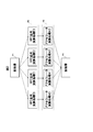
- FIG. 1 is a block diagram showing a configuration of an SoC to which the electronic arithmetic unit according to the first embodiment is applied.
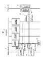
- FIG. 2 is a block diagram showing a periodic processing flow executed by the SoC of FIG.
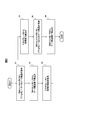
- FIG. 3 is a flowchart showing the accelerator management process.
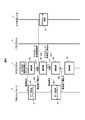
- FIG. 4 is a sequence diagram showing a processing flow accompanied by an interrupt to the core using the accelerator.
- FIG. 5 is a sequence diagram showing a processing flow without interrupting the core using the accelerator.
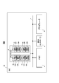
- FIG. 6 is a block diagram showing a configuration of an SoC to which the electronic arithmetic unit according to the second embodiment is applied.
- FIG. 7 is a sequence diagram showing a processing flow of the DMA controller, the CPU cluster, and the accelerator of FIG.
- FIG. 1 is a block diagram showing a configuration of an SoC to which the electronic arithmetic unit according to the first embodiment is applied.
- the SoC1 includes an HPC (High Performance Core) cluster 2, an LPC (Low Performance Core) cluster 3, a memory 4, a DMA (Direct Memory Access) controller 5, and an accelerator 6.
- the HPC cluster 2, the LPC cluster 3, the memory 4, the DMA controller 5, and the accelerator 6 are connected to each other via the internal bus 7.
- the HPC cluster 2 is the first computational resource that executes the first processing
- the accelerator 6 is the second computational resource that executes the second processing
- the LPC cluster 3 is the execution of the second processing by the second computational resource. It can be used as a third computational resource to manage.
- HPC cluster 2 is a set of CPU cores (hereinafter referred to as HPC) having relatively high processing performance.
- the LPC cluster 3 is a set of CPU cores (hereinafter referred to as LPCs) having relatively low processing performance.
- the SoC1 has a terrorist configuration having a plurality of CPU cores (application cores) having different processing performances.
- HPC cluster 2 includes HPCs 20 to 23. Each HPC 20 to 23 can execute general-purpose processing described in the program. Each HPC 20 to 23 includes arithmetic processing units HA0 to HA3.
- Each arithmetic processing unit HA0 to HA3 executes arithmetic processing. At this time, each arithmetic processing unit HA0 to HA3 can execute arithmetic processing in parallel. Further, each arithmetic processing unit HA0 to HA3 can call the accelerator 6 and cause the accelerator 6 to execute a specific process. By causing the accelerator 6 to execute the specific processing by the arithmetic processing units HA0 to HA3, the arithmetic load of the HPCs 20 to 23 can be reduced. The arithmetic processing by the arithmetic processing units HA0 to HA3 and the specific processing by the accelerator 6 can be executed in parallel.
- the LPC cluster 3 includes LPCs 30 to 33.
- Each LPC 30 to 33 includes management processing units LB0 to LB3.
- the management processing units LB0 to LB3 manage the execution of the specific processing by the accelerator 6 when the arithmetic processing units HA0 to HA3 cause the accelerator 6 to execute the specific processing. At this time, the management processing units LB0 to LB3 can give the DMA controller 5 and the accelerator 6 a series of commands for causing the accelerator 6 to execute the specific processing.
- the memory 4 can be composed of, for example, a semiconductor memory such as SRAM or DRAM.
- the memory 4 is provided with a work area for storing programs being executed by each HPC 20 to 23, each LPC 30 to 33 and the accelerator 6, and for each HPC 20 to 23, each LPC 30 to 33 and the accelerator 6 to execute a program. Can be done.
- the DMA controller 5 controls the DMA transfer when transferring data between each HPC 20 to 23 and the accelerator 6. At this time, the DMA controller 5 can operate as an interrupt controller.
- Accelerator 6 executes a specific process.
- This specific process can be a process with a heavier load than the process executed by HPCs 20 to 23.
- This specific processing is, for example, deep learning, matrix operation, image processing, or the like.
- the accelerator 6 may be a CPU having a plurality of cores, or may be dedicated hardware such as an ASIC (Application Specific Integrated Circuit) or an FPGA (Field-Programmable Gate Array). When a CPU having a plurality of cores is used as the accelerator 6, a specific process can be executed based on a program.
- ASIC Application Specific Integrated Circuit
- FPGA Field-Programmable Gate Array
- FIG. 2 is a block diagram showing a periodic processing flow executed by the SoC of FIG.
- the HPC cluster 2 of FIG. 1 executes the HPC parallel arithmetic processing P2 after executing the preprocessing P1.
- the HPC cluster 2 calls the accelerator process P3 in the HPC parallel computing process P2, and executes the post-process P4 after the accelerator process P3.
- each of the HPCs 20 to 23 in FIG. 1 executes the HPC parallel computing processes E0 to E3, and individually calls the accelerator computing processes A0 to A3 from the HPC parallel computing processes E0 to E3. It is assumed that the OS (Operating System) processing is performed on the LPC cluster 3.
- OS Operating System
- the accelerator management process can be executed by any one of the management processing units LB0 to LB3 of each LPC 30 to 33.
- the OS can specify the management processing units LB0 to LB3 that execute the accelerator management processing.
- the OS can select the management processing units LB0 to LB3 that execute the accelerator management processing based on the processing load being executed by each LPC 30 to 33.
- FIG. 3 is a flowchart showing the accelerator management process.
- each core using the accelerator 6 of FIG. 1 instructs the DMA controller 5 to transfer data to the accelerator 6 (S1).
- the DMA controller 5 executes a data transfer completion interrupt for each core (S2).
- each core on which the data transfer completion interrupt is executed instructs the accelerator 6 to start processing (S3).
- the accelerator 6 executes a processing completion interrupt for each core instructed to start processing (S4).
- each core on which the processing completion interrupt is executed instructs the DMA controller 5 to transfer data from the accelerator 6 (S5).
- the DMA controller 5 executes a data transfer completion interrupt for each core instructed to transfer data (S6).
- FIG. 4 is a sequence diagram showing a processing flow accompanied by an interrupt to the core using the accelerator. Note that FIG. 4 focuses on one HPC20 in the HPC cluster 2 of FIG. 1, and shows an example in which the HPC20 using the accelerator 6 performs the accelerator management process.
- the HPC 20 of FIG. 1 instructs the DMA controller 5 to transfer data to the accelerator 6 when the HPC parallel computing process E0 is completed (S1A).
- the DMA controller 5 executes data transfer to the accelerator 6 (K1).
- the HPC cluster 2 can execute other processing K2 such as another application.
- the DMA controller 5 executes a data transfer completion interrupt to the HPC 20 (S2A).
- the HPC 20 interrupts the other process K2, executes the process K11 that gives the accelerator process start instruction, and then executes the accelerator process start instruction (S3A).
- the accelerator 6 executes the accelerator processing P3 instructed by the HPC 20, and then executes an accelerator processing completion interrupt to the HPC 20 (S4A). While the accelerator 6 is executing the process instructed by the HPC 20, the HPC cluster 2 can execute another process K3 such as another application.
- the HPC 20 interrupts the other processing K3, executes the processing K12 for instructing the DMA controller 5 to transfer data from the accelerator 6, and then transfers the data from the accelerator 6. (S5A).
- the DMA controller 5 executes the data transfer from the accelerator 6 (K5).
- the HPC cluster 2 can execute other processing K6 such as another application.
- the DMA controller 5 executes a data transfer completion interrupt to the HPC 20 (S6A).
- the HPC 20 interrupts the other process K6 when the data transfer completion interrupt is executed.
- the HPC 20 can execute another application while the DMA controller 5 or the accelerator 6 is operating.
- the HPC 20 is interrupted three times by the completion of the post-processing P4, the interrupt handler operates each time the interrupt is performed, and the processing is interrupted by the context switch.
- the context switch overhead not only the context switch overhead but also the cache hit rate in other processing K2 and K3 decreases due to the execution of other processing K11 and K12 after the interruption of other processing K2 and K3. As a result, the effective performance is reduced.
- FIG. 5 is a sequence diagram showing a processing flow that does not involve an interrupt to the core that uses the accelerator.
- four HPCs 20 to 23 in the HPC cluster 2 of FIG. 1 execute parallel processing using the accelerator 6, and any of the LPCs 30 to 33 in the LPC cluster 3 performs the accelerator management processing. Indicated.
- each HPC 20 to 23 is all after the execution of the HPC parallel arithmetic processes E0 to E3 except when the post-process P4 is executed.
- Other processes K2, K3, and K6 can be executed in the time of.
- each HPC 20 to 23 instructs the DMA controller 5 to transfer data to the accelerator 6 when the HPC parallel computing processes E0 to E3 are completed (S1B).
- the DMA controller 5 executes data transfer to the accelerator 6 when the data transfer to the accelerator 6 is instructed by the HPCs 20 to 23 (K1). During the data transfer to the accelerator 6, each HPC 20 to 23 can execute other processes such as another application in parallel.
- the DMA controller 5 executes a data transfer completion interrupt to the LPC 30 in the LPC cluster 3 (S2B).
- the LPC 30 in the LPC cluster 3 executes an instruction to start the accelerator processing P3 to the accelerator 6 (S3B). At this time, each HPC 20 to 23 can be continuously executed without interrupting other processing such as another application.
- the accelerator 6 executes the accelerator processing P3 instructed by the LPC 30 in the LPC cluster 3, and then executes an accelerator processing completion interrupt for the LPC 30 (S4B).
- the accelerator process P3 the accelerator arithmetic processes A0 to A3 called from the HPCs 20 to 23 are executed in parallel. While the accelerator 6 is executing the process instructed by the LPC 30, each HPC 20 to 23 can execute other processes such as another application in parallel.
- the LPC 30 in the LPC cluster 3 executes an instruction for data transfer from the accelerator 6 to the DMA controller 5 (S5B). At this time, each HPC 20 to 23 can be continuously executed without interrupting other processing such as another application.
- the DMA controller 5 executes the data transfer from the accelerator 6 (K5).
- each HPC 20 to 23 can execute other processes such as another application in parallel.
- the DMA controller 5 executes a data transfer completion interrupt to the LPC 30 in the LPC cluster 3 (S6B). At this time, each HPC 20 to 23 can be continuously executed without interrupting other processing such as another application.
- each HPC 20 to 23 can be continuously executed without interrupting other processing by the interrupt processing generated in S2B, S4B, and S6B. Therefore, since the cache hit rate is maintained by a certain amount and the context switch does not occur, it is possible to suppress the deterioration of the execution performance due to the use of the accelerator 6.
- each of the LPCs 30 to 33 cores in the LPC cluster 3 is mainly assigned to event-driven processing with a relatively low load, the decrease in execution performance due to the increase in interrupt processing to the LPC cluster 3 is caused by the HPC cluster. Compared to that, it is sufficiently low, and the processing performance of the entire SoC1 can be relatively improved.
- the data transfer completion interrupt (S6B) from the DMA controller 5 is processed by any of the LPCs 30 to 33 in the LPC cluster, and after confirming the completion of the accelerator processing P3, the HPC cluster undergoes an OS event.
- An example of notifying any of HPCs 20 to 23 in 2 of the start of post-processing P4 is assumed, but it is not always necessary to take the procedure described in this embodiment.
- any LPC 30 to 33 in the LPC cluster 3 can substitute polling for the accelerator 6, and the HPC cluster 2 suitable for high-performance processing performs other processing. By making it executable, it is possible to improve the processing performance of the entire SoC1.
- a user who uses SoC1 may need to write a program for realizing the above procedure. That is, when it is necessary to explicitly indicate the core that performs the accelerator management process in the accelerator management process including a series of commands, it can be described in the source code of the user application by using the following pragma description, for example. Is. # Programa AccManagement LPC # 1
- a pragma for designating a core for performing accelerator management processing is used, and then the core is specified.
- the first core (LPC # 1) in the LPC cluster 3 is used instead of the core in the HPC cluster 2.
- the above pragma method is taken as an example, but for example, the argument of the accelerator calling function may include the above core designation, and the core that performs the accelerator management process is explicitly shown.
- the method is not limited to the above pragma method.
- FIG. 6 is a block diagram showing a configuration of an SoC to which the electronic arithmetic unit according to the second embodiment is applied.
- the SoC 11 includes a CPU cluster 8, a memory 4, a DMA controller 5, and an accelerator 6.
- the CPU cluster 8, the memory 4, the DMA controller 5, and the accelerator 6 are connected to each other via the internal bus 7.
- the CPC cluster 8 is a set of CPU cores.
- the SoC 11 has a homogeneous configuration having a plurality of CPU cores (application cores) having no difference in processing performance.
- some CPU cores of the CPC cluster 8 are the first computational resources that execute the first process
- the accelerator 6 is the second computational resources that execute the second process
- the other CPU cores of the CPC cluster 8 are the second computational resources. It can be used as a third computational resource that manages the execution of the second process by the resource.
- the CPC cluster 8 includes CPU cores 80 to 83.
- the CPU cores 80 to 83 can execute general-purpose processing described in the program.
- Each CPU core 80 to 83 includes arithmetic processing units CA0 to CA3 and management processing units CB0 to CB3.
- Each arithmetic processing unit CA0 to CA3 executes arithmetic processing. At this time, each arithmetic processing unit CA0 to CA3 can execute arithmetic processing in parallel. Further, each arithmetic processing unit CA0 to CA3 can call the accelerator 6 and cause the accelerator 6 to execute a specific process. The arithmetic processing by the arithmetic processing units CA0 to CA3 and the specific processing by the accelerator 6 can be executed in parallel.
- the management processing units CB0 to CB3 manage the execution of the specific processing by the accelerator 6 when the arithmetic processing units CA0 to CA3 cause the accelerator 6 to execute the specific processing. At this time, the management processing units CB0 to CB3 can give the DMA controller 5 and the accelerator 6 a series of commands for causing the accelerator 6 to execute the specific processing.
- the CPC cluster 8 executes the CPU parallel arithmetic processing after executing the preprocessing in the same manner as the processing of FIG.
- the CPC cluster 8 calls the accelerator processing in the CPU parallel computing processing, and executes post-processing after the accelerator processing.
- Each CPU core 80 to 83 executes CPU parallel arithmetic processing, and individually calls accelerator arithmetic processing from each CPU parallel arithmetic processing. It is assumed that the OS (Operating System) processing is performed by any of the CPU cores 80 to 83 in the CPC cluster 8.
- OS Operating System
- FIG. 7 is a sequence diagram showing a processing flow of the DMA controller, the CPU cluster, and the accelerator of FIG.
- four CPU cores 80 to 83 in the CPU cluster 8 of FIG. 6 execute parallel processing using the accelerator 6, and one CPU core 80 in the CPU cluster 8 performs accelerator management processing. showed that.
- each CPU core 81 to 83 excludes the post-process P4 after the CPU parallel arithmetic processes C1 to C3.
- Other processes K2, K3, and K6 can be executed at all times.
- each CPU core 80 to 83 instructs the DMA controller 5 to transfer data to the accelerator 6 when the CPU parallel computing processes C0 to C3 are completed (S1C).
- the DMA controller 5 executes the data transfer to the accelerator 6 (K1).
- each CPU core 81 to 83 can execute other processes such as another application in parallel.
- the DMA controller 5 executes a data transfer completion interrupt to the CPU core 80 in the CPU cluster 8 (S2C).
- the CPU core 80 in the CPU cluster 8 executes an instruction to start the accelerator processing P3 to the accelerator 6 (S3C). At this time, each CPU core 81 to 83 can be continuously executed without interrupting other processing such as another application.
- the accelerator 6 executes the accelerator processing P3 instructed by the CPU core 80 in the CPU cluster 8, and then executes an accelerator processing completion interrupt for the CPU core 80 (S4C).
- the accelerator processing P3 the accelerator arithmetic processing A0 to A3 called from the CPU cores 80 to 83 are executed in parallel. While the accelerator 6 is executing the process instructed by the CPU core 80, each CPU core 81 to 83 can execute other processes such as another application in parallel.
- the CPU core 80 in the CPU cluster 8 executes an instruction to transfer data from the accelerator 6 to the DMA controller 5 (S5C). At this time, each CPU core 81 to 83 can be continuously executed without interrupting other processing such as another application.
- the DMA controller 5 executes the data transfer from the accelerator 6 (K5).
- each CPU core 81 to 83 can execute other processes such as another application in parallel.
- the DMA controller 5 executes a data transfer completion interrupt to the CPU core 80 in the CPU cluster 8 (S6C). At this time, each CPU core 81 to 83 can be continuously executed without interrupting other processing such as another application.
- each CPU core 81 to 83 can be continuously executed without interrupting other processing by the interrupt processing generated in S2C, S4C, and S6C. Therefore, since the cache hit rate is maintained to a certain extent and no context switch is generated, it is possible to suppress a decrease in execution performance due to the use of the accelerator 6.
- various event-driven processing (OS processing and other interrupt processing) is not specified, but by making the core that executes accelerator management processing the same core as the core that performs various event-driven processing. , It is possible to improve the utilization efficiency of other cores.
- the number of cores capable of continuing the processing can be increased as in the first embodiment, so that the processing performance can be improved.
- the present invention is not limited to the above-described embodiment, and includes various modifications.
- the above-described embodiment has been described in detail in order to explain the present invention in an easy-to-understand manner, and is not necessarily limited to the one including all the described configurations.
- it is possible to replace a part of the configuration of one embodiment with the configuration of another embodiment and it is also possible to add the configuration of another embodiment to the configuration of one embodiment.
- each of the above configurations, functions, processing units, processing means and the like may be realized by hardware by designing a part or all of them by, for example, an integrated circuit.
- 1 SoC 1 SoC, 2 HPC cluster, 3 LPC cluster, 4 memory, 5 DMA controller, 6 accelerator
Landscapes
- Engineering & Computer Science (AREA)
- Theoretical Computer Science (AREA)
- Software Systems (AREA)
- Physics & Mathematics (AREA)
- General Engineering & Computer Science (AREA)
- Computer Hardware Design (AREA)
- General Physics & Mathematics (AREA)
- Computing Systems (AREA)
- Microelectronics & Electronic Packaging (AREA)
- Mathematical Physics (AREA)
- Advance Control (AREA)
- Multi Processors (AREA)
- Microcomputers (AREA)
Abstract
電子演算装置の演算効率を向上させる。各HPC20~23は、演算処理部HA0~HA3を備え、各演算処理部HA0~HA3は、演算処理を並列実行し、各LPC30~33は、管理処理部LB0~LB3を備え、各管理処理部LB0~LB3は、各演算処理部HA0~HA3がアクセラレータ6に特定処理を実行させるときに、アクセラレータ6による特定処理の実行を管理し、アクセラレータ6に特定処理を実行させるための一連の指令をDMAコントローラ5およびアクセラレータ6に行う。
Description
本発明は、電子制御装置(Electronic Control Unit、以下、ECUと言う)などに適用可能な電子演算装置に関する。
近年、産業用電子制御装置を支えるシステムの開発において、制御性能の向上、厳格化する規制への対応および装置の自律化に伴う制御演算処理の増大というアプリケーションの高負荷化が進んでいる。このような高負荷化に対応して、ECUにおいてもメニーコア化およびアクセラレータの利用などの高性能化を実現するために、マルチコアもしくはメニーコアを有するプロセッサ、メモリなどの周辺資源およびアクセラレータ等を混載したSoC(System on Chip)が登場し、電子演算装置の複雑化が進んでいる。
一方、組込み分野においては、前段のコントローラにおける制御演算結果を後段のコントローラもしくはアクチュエータに規定のタイミングで伝達する必要から、強いリアルタイム制約が存在する。このため、アプリケーションの高負荷化に伴う制御装置の複雑化と、リアルタイム制約の遵守とを両立させた電子演算装置の利用方式が求められる。
特許文献1では、特に、リアルタイム性に着目した高応答化の観点から、マルチコアプロセッサに対してコア負荷率を意図的に調整し、高応答性を実現する方式が開示されている。
しかしながら、特許文献1に開示された方式では、リアルタイム性を強く意識する一方で、組込み分野におけるアプリケーションの高負荷化の背景と、適用先に応じた競合軸として消費電力、コストおよび発熱量などの要件が、必ずしも十全に考慮されていない。
自律システムを例にすると、特に、周辺環境の認識から自身の動作計画までを行うアプリケーションの負荷増が激しいが、これらアプリケーションは、周期的なセンシングに基づく周期的な処理となる。このような周期的な処理に対し、周辺環境に危害を加えかねない状況における緊急停止などの状況発生に対し、即応性が求められる処理は、イベント駆動型の処理と言える。どちらの処理も、一定のリアルタイム性が求められるが、前者は負荷増の観点からスループットにも重きが置かれる。
本発明は、上記事情に鑑みなされたものであり、その目的は、演算効率を向上させることが可能な電子演算装置を提供することにある。
上記目的を達成するため、第1の観点に係る電子演算装置は、第1処理を実行する第1計算資源と、第2処理を実行する第2計算資源と、前記第1計算資源からの前記第2計算資源の呼び出しに基づいて、前記第2計算資源による前記第2処理の実行を管理する第3計算資源とを備える。
本発明によれば、電子演算装置の演算効率を向上させることができる。
実施形態について、図面を参照して説明する。なお、以下に説明する実施形態は特許請求の範囲に係る発明を限定するものではなく、また、実施形態の中で説明されている諸要素およびその組み合わせの全てが発明の解決手段に必須であるとは限らない。
図1は、第1実施形態に係る電子演算装置が適用されるSoCの構成を示すブロック図である。
図1において、SoC1は、HPC(High Performance Core)クラスタ2、LPC(Low Performance Core)クラスタ3、メモリ4、DMA(Direct Memory Access)コントローラ5およびアクセラレータ6を備える。HPCクラスタ2、LPCクラスタ3、メモリ4、DMAコントローラ5およびアクセラレータ6は、内部バス7を介して相互に接続されている。ここで、HPCクラスタ2は、第1処理を実行する第1計算資源、アクセラレータ6は、第2処理を実行する第2計算資源、LPCクラスタ3は、第2計算資源による第2処理の実行を管理する第3計算資源として用いることができる。
図1において、SoC1は、HPC(High Performance Core)クラスタ2、LPC(Low Performance Core)クラスタ3、メモリ4、DMA(Direct Memory Access)コントローラ5およびアクセラレータ6を備える。HPCクラスタ2、LPCクラスタ3、メモリ4、DMAコントローラ5およびアクセラレータ6は、内部バス7を介して相互に接続されている。ここで、HPCクラスタ2は、第1処理を実行する第1計算資源、アクセラレータ6は、第2処理を実行する第2計算資源、LPCクラスタ3は、第2計算資源による第2処理の実行を管理する第3計算資源として用いることができる。
HPCクラスタ2は、相対的に処理性能が高いCPUコア(以下、HPCと言う)の集合である。LPCクラスタ3は、相対的に処理性能が低いCPUコア(以下、LPCと言う)の集合である。このとき、SoC1は、処理性能が異なる複数のCPUコア(アプリケーションコア)を有するテロジニアスな構成となる。
このSoC1上において、周期的に動作するアプリケーションと、イベントを契機として動作するアプリケーションの2種類のアプリケーションが動作する。このとき、相対的に負荷の重い周期処理をHPCを中心に割り当て、負荷の比較的低いイベント駆動処理をLPCを中心に割当てることができる。
HPCクラスタ2は、HPC20~23を備える。各HPC20~23は、プログラムで記述される汎用処理を実行することができる。各HPC20~23は、演算処理部HA0~HA3を備える。
各演算処理部HA0~HA3は、演算処理を実行する。このとき、各演算処理部HA0~HA3は、演算処理を並列実行することができる。また、各演算処理部HA0~HA3は、アクセラレータ6を呼び出し、アクセラレータ6に特定処理を実行させることができる。各演算処理部HA0~HA3がアクセラレータ6に特定処理を実行させることにより、各HPC20~23の演算負荷を軽減することができる。各演算処理部HA0~HA3による演算処理と、アクセラレータ6による特定処理は、並列実行することができる。
LPCクラスタ3は、LPC30~33を備える。各LPC30~33は、管理処理部LB0~LB3を備える。
各管理処理部LB0~LB3は、各演算処理部HA0~HA3がアクセラレータ6に特定処理を実行させるときに、アクセラレータ6による特定処理の実行を管理する。このとき、管理処理部LB0~LB3は、アクセラレータ6に特定処理を実行させるための一連の指令をDMAコントローラ5およびアクセラレータ6に行うことができる。
メモリ4は、例えば、SRAMまたはDRAMなどの半導体メモリから構成することができる。メモリ4には、各HPC20~23、各LPC30~33およびアクセラレータ6が実行中のプログラムを格納したり、各HPC20~23、各LPC30~33およびアクセラレータ6がプログラムを実行するためのワークエリアを設けたりすることができる。
DMAコントローラ5は、各HPC20~23とアクセラレータ6との間のデータ転送に際してDMA転送を制御する。このとき、DMAコントローラ5は、割り込みコントローラとして動作することができる。
アクセラレータ6は、特定処理を実行する。この特定処理は、HPC20~23で実行される処理よりも負荷の重い処理とすることができる。この特定処理は、例えば、ディープラーニング、行列演算または画像処理などである。アクセラレータ6は、複数のコアを備えるCPUであってもよいし、ASIC(Application Specific Integrated Circuit)またはFPGA(Field-Programmable Gate Array)などの専用ハードウェアであってもよい。アクセラレータ6として複数のコアを備えるCPUを用いた場合、プログラムに基づいて特定処理を実行させることができる。
図2は、図1のSoCで実行される周期的な処理の流れを示すブロック図である。
図2において、図1のHPCクラスタ2は、前処理P1を実行した後、HPC並列演算処理P2を実行する。HPCクラスタ2は、HPC並列演算処理P2において、アクセラレータ処理P3を呼び出し、アクセラレータ処理P3後に後処理P4を実行する。
図2において、図1のHPCクラスタ2は、前処理P1を実行した後、HPC並列演算処理P2を実行する。HPCクラスタ2は、HPC並列演算処理P2において、アクセラレータ処理P3を呼び出し、アクセラレータ処理P3後に後処理P4を実行する。
HPC並列演算処理P2では、図1の各HPC20~23は、HPC並列演算処理E0~E3を実行し、各HPC並列演算処理E0~E3からアクセラレータ演算処理A0~A3を個別に呼び出す。なお、OS(Operating System)処理は、LPCクラスタ3上にて行われているものとする。
HPCクラスタ2内の各HPC20~23と、アクセラレータ6を非同期に動作させて処理を行う場合、アクセラレータ6を動作させる際には、以下の一連の手順が必要となる。この一連の手順を、アクセラレータ管理処理と呼ぶ。アクセラレータ管理処理は、各LPC30~33の管理処理部LB0~LB3のいずれか1つが実行することができる。アクセラレータ管理処理を実行する管理処理部LB0~LB3は、OSが指定することができる。OSは、各LPC30~33が実行中の処理の負荷に基づいて、アクセラレータ管理処理を実行する管理処理部LB0~LB3を選択することできる。
図3は、アクセラレータ管理処理を示すフローチャートである。
図3において、図1のアクセラレータ6を利用する各コアは、DMAコントローラ5に対し、アクセラレータ6へのデータ転送を指示する(S1)。
図3において、図1のアクセラレータ6を利用する各コアは、DMAコントローラ5に対し、アクセラレータ6へのデータ転送を指示する(S1)。
次に、DMAコントローラ5は、S1で指示されたデータ転送が完了すると、各コアに対し、データ転送完了割込みを実行する(S2)。
次に、データ転送完了割込みが実行された各コアは、アクセラレータ6に対し、処理の開始を指示する(S3)。
次に、アクセラレータ6は、処理の開始を指示した各コアに対し、処理完了割込みを実行する(S4)。
次に、処理完了割込みが実行された各コアは、DMAコントローラ5に対し、アクセラレータ6からのデータ転送を指示する(S5)。
次に、DMAコントローラ5は、データ転送を指示した各コアに対し、データ転送完了割込みを実行する(S6)。
図4は、アクセラレータを利用するコアへの割り込みを伴う処理の流れを示すシーケンス図である。なお、図4では、図1のHPCクラスタ2内の1つのHPC20に着目し、アクセラレータ6を利用するHPC20がアクセラレータ管理処理を行う例を示した。
図4において、図1のHPC20は、HPC並列演算処理E0が完了すると、DMAコントローラ5に対し、アクセラレータ6へのデータ転送を指示する(S1A)。
DMAコントローラ5は、アクセラレータ6へのデータ転送がHPC20から指示されると、アクセラレータ6に対するデータ転送を実行する(K1)。アクセラレータ6へのデータ転送中は、HPCクラスタ2は、別のアプリケーションなどの他処理K2を実行することができる。
次に、DMAコントローラ5は、HPC20から指示されたデータ転送が完了すると、HPC20に対し、データ転送完了割込みを実行する(S2A)。このとき、HPC20は、他処理K2を中断し、アクセラレータ処理開始指示を行う処理K11を実行した上で、アクセラレータ処理開始指示を実行する(S3A)。
次に、アクセラレータ6は、HPC20から指示されたアクセラレータ処理P3を実行した後、HPC20に対し、アクセラレータ処理完了割込みを実行する(S4A)。HPC20から指示された処理をアクセラレータ6が実行中は、HPCクラスタ2は、別のアプリケーションなどの他処理K3を実行することができる。
HPC20は、アクセラレータ処理完了割込みが実行されると、他処理K3を中断し、DMAコントローラ5に対し、アクセラレータ6からのデータ転送の指示を行う処理K12を実行した上で、アクセラレータ6からのデータ転送の指示を実行する(S5A)。
DMAコントローラ5は、アクセラレータ6からのデータ転送がHPC20から指示されると、アクセラレータ6からのデータ転送を実行する(K5)。アクセラレータ6からのデータ転送中は、HPCクラスタ2は、別のアプリケーションなどの他処理K6を実行することができる。
次に、DMAコントローラ5は、アクセラレータ6からのデータ転送が完了すると、HPC20に対し、データ転送完了割込みを実行する(S6A)。HPC20は、データ転送完了割込みが実行されると、他処理K6を中断する。
以上から、HPC20とアクセラレータ6が非同期的に動作することにより、DMAコントローラ5またはアクセラレータ6の動作中にHPC20は別のアプリケーションを実行することが可能となる。このとき、HPC20には、後処理P4の完了までに3度の割込み処理が入り、割込みの度に割込みハンドラが動作し、コンテキストスイッチにより処理が中断する。処理の中断による影響としては、コンテキストスイッチのオーバヘッドのみならず、他処理K2、K3の中断後に別の処理K11、K12が実行されることによる他処理K2、K3でのキャッシュヒット率が低下し、それにより実効性能が低下する。
図5は、アクセラレータを利用するコアへの割り込みを伴わない処理の流れを示すシーケンス図である。なお、図5では、図1のHPCクラスタ2内の4つのHPC20~23がアクセラレータ6を利用する並列処理を実行し、LPCクラスタ3内のいずれかのLPC30~33がアクセラレータ管理処理を行う例を示した。
また、図5では、図4の他処理K2、K3、K6は記載していないが、各HPC20~23は、HPC並列演算処理E0~E3の実行後は、後処理P4の実行時を除く全ての時間で他処理K2、K3、K6が実行可能となる。
図5において、図3に示したアクセラレータ管理処理のうちS2からS6までに対応する処理が、アクセラレータ6を利用するHPC20~23から分離され、LPCクラスタ3内のいずれかのLPC30~33に割り当てられる。以下の説明では、アクセラレータ管理処理がLPCクラスタ3内のLPC30に割り当てられている場合を例にとる。
すなわち、各HPC20~23は、HPC並列演算処理E0~E3が完了すると、DMAコントローラ5に対し、アクセラレータ6へのデータ転送を指示する(S1B)。
DMAコントローラ5は、アクセラレータ6へのデータ転送が各HPC20~23から指示されると、アクセラレータ6に対するデータ転送を実行する(K1)。アクセラレータ6へのデータ転送中は、各HPC20~23は、別のアプリケーションなどの他処理を並列実行することができる。
次に、DMAコントローラ5は、各HPC20~23から指示されたデータ転送が完了すると、LPCクラスタ3内のLPC30に対し、データ転送完了割込みを実行する(S2B)。
次に、LPCクラスタ3内のLPC30は、データ転送完了割込みが実行されると、アクセラレータ6に対し、アクセラレータ処理P3の開始指示を実行する(S3B)。このとき、各HPC20~23は、別のアプリケーションなどの他処理を中断することなく継続して実行することができる。
次に、アクセラレータ6は、LPCクラスタ3内のLPC30から指示されたアクセラレータ処理P3を実行した後、そのLPC30に対し、アクセラレータ処理完了割込みを実行する(S4B)。このアクセラレータ処理P3では、各HPC20~23から呼び出されたアクセラレータ演算処理A0~A3が並列実行される。LPC30から指示された処理をアクセラレータ6が実行中は、各HPC20~23は、別のアプリケーションなどの他処理を並列実行することができる。
LPCクラスタ3内のLPC30は、アクセラレータ処理完了割込みが実行されると、DMAコントローラ5に対し、アクセラレータ6からのデータ転送の指示を実行する(S5B)。このとき、各HPC20~23は、別のアプリケーションなどの他処理を中断することなく継続して実行することができる。
DMAコントローラ5は、アクセラレータ6からのデータ転送がLPC30から指示されると、アクセラレータ6からのデータ転送を実行する(K5)。アクセラレータ6からのデータ転送中は、各HPC20~23は、別のアプリケーションなどの他処理を並列実行することができる。
次に、DMAコントローラ5は、アクセラレータ6からのデータ転送が完了すると、LPCクラスタ3内のLPC30に対し、データ転送完了割込みを実行する(S6B)。このとき、各HPC20~23は、別のアプリケーションなどの他処理を中断することなく継続して実行することができる。
これにより、各HPC20~23は、S2B、S4B、S6Bにて発生する割込み処理により他処理を中断することなく継続して実行することができる。このため、キャッシュヒット率が一定量維持され、コンテキストスイッチも発生しないことから、アクセラレータ6の利用による実行性能の低下を抑制することができる。
また、LPCクラスタ3内の各LPC30~33コアには、負荷の比較的低いイベント駆動処理を中心に割り当てられることから、LPCクラスタ3への割込み処理の増大による実行性能の低下は、HPCクラスタのそれに比べて十分に低く、SoC1全体での処理性能を相対的に向上させることができる。
なお、図5では、DMAコントローラ5からのデータ転送完了割込み(S6B)をLPCクラスタ内のいずれかのLPC30~33にて処理し、アクセラレータ処理P3の完了を確認の上でOSイベントを経てHPCクラスタ2内のいずれかのHPC20~23に後処理P4の開始を通知する例を想定しているが、必ずしも本実施形態で説明した手順をとる必要はない。
また、本実施形態では、CPUコアとアクセラレータを非同期に実行させる例を示したが、別実施形態として、CPUコアとアクセラレータを同期させて処理を行う方法をとることも可能である。CPUコアとアクセラレータを同期的に実行させる場合、各CPUコアがアクセラレータに対して定期的にアクセスし、終了状況を確認するポーリングを行う例が想定される。別実施形態では、このようなケースにおいても、LPCクラスタ3内のいずれかのLPC30~33にアクセラレータ6へのポーリングを代替させることができ、高性能な処理に適したHPCクラスタ2において他処理を実行可能とすることで、SoC1全体での処理性能の向上を図ることができる。
SoC1を利用するユーザは、以上の手順を実現するためのプログラムを記述する必要がある可能性がある。すなわち、一連の指令を含むアクセラレータ管理処理にあたり、アクセラレータ管理処理を行うコアを明示的に示す必要がある場合、例えば、以下のようなプラグマ記述を用い、ユーザアプリケーションのソースコードに記述することが可能である。
#pragma AccManagement LPC#1
#pragma AccManagement LPC#1
上記のプラグマ記述は、例えば、アクセラレータ管理処理を行うコアを指定するためのプラグマ(AccManagement)を用い、その後にコアを指定する。この例では、HPCクラスタ2内のコアではなく、LPCクラスタ3内の1番目のコア(LPC#1)を用いることを示す。
この他、プラグマ記述方式には様々な形態があり、例えば、LPCクラスタ3内のいずれのコアを用いてもよい場合、HPCクラスタ2およびLPCクラスタ3内の任意のコアを利用できる場合、アクセラレータを呼び出す処理を行うコア自身が管理する場合など、様々な利用方式が想定される。
本例では、それぞれの利用方式に応じて以下のような記述が可能である。
#pragma AccManagement LPC#any#pragma AccManagement any#pragma AccManagement self
#pragma AccManagement LPC#any#pragma AccManagement any#pragma AccManagement self
なお、本実施形態では、上記のプラグマ方式を例とするが、例えば、アクセラレータ呼出し関数の引数に上記のコア指定を含む例などであってもよく、アクセラレータ管理処理を行うコアを明示的に示す方式については、上記のプラグマ方式に限らない。
また、上記した実施形態において、2種類のCPUコア構成およびプログラミングモデルとしてのプラグマ記述方式を例示しているが、本発明はこれに限定されるものではない。
図6は、第2実施形態に係る電子演算装置が適用されるSoCの構成を示すブロック図である。
図6において、SoC11は、CPUクラスタ8、メモリ4、DMAコントローラ5およびアクセラレータ6を備える。CPUクラスタ8、メモリ4、DMAコントローラ5およびアクセラレータ6は、内部バス7を介して相互に接続されている。このSoC11上において、周期的に動作するアプリケーションと、イベントを契機として動作するアプリケーションの2種類のアプリケーションが動作する。
図6において、SoC11は、CPUクラスタ8、メモリ4、DMAコントローラ5およびアクセラレータ6を備える。CPUクラスタ8、メモリ4、DMAコントローラ5およびアクセラレータ6は、内部バス7を介して相互に接続されている。このSoC11上において、周期的に動作するアプリケーションと、イベントを契機として動作するアプリケーションの2種類のアプリケーションが動作する。
CPCクラスタ8は、CPUコアの集合である。このとき、SoC11は、処理性能に差がない複数のCPUコア(アプリケーションコア)を有するホモジニアスな構成となる。ここで、CPCクラスタ8の一部のCPUコアは第1処理を実行する第1計算資源、アクセラレータ6は第2処理を実行する第2計算資源、CPCクラスタ8の他のCPUコアは第2計算資源による第2処理の実行を管理する第3計算資源として用いることができる。
CPCクラスタ8は、CPUコア80~83を備える。CPUコア80~83は、プログラムで記述される汎用処理を実行することができる。各CPUコア80~83は、演算処理部CA0~CA3および管理処理部CB0~CB3を備える。
各演算処理部CA0~CA3は、演算処理を実行する。このとき、各演算処理部CA0~CA3は、演算処理を並列実行することができる。また、各演算処理部CA0~CA3は、アクセラレータ6を呼び出し、アクセラレータ6に特定処理を実行させることができる。各演算処理部CA0~CA3による演算処理と、アクセラレータ6による特定処理は、並列実行することができる。
各管理処理部CB0~CB3は、各演算処理部CA0~CA3がアクセラレータ6に特定処理を実行させるときに、アクセラレータ6による特定処理の実行を管理する。このとき、管理処理部CB0~CB3は、アクセラレータ6に特定処理を実行させるための一連の指令をDMAコントローラ5およびアクセラレータ6に行うことができる。
CPCクラスタ8は、図2の処理と同様に、前処理を実行した後、CPU並列演算処理を実行する。CPCクラスタ8は、CPU並列演算処理において、アクセラレータ処理を呼び出し、アクセラレータ処理後に後処理を実行する。
各CPUコア80~83は、CPU並列演算処理を実行し、各CPU並列演算処理からアクセラレータ演算処理を個別に呼び出す。なお、OS(Operating System)処理は、CPCクラスタ8内のいずれかのCPUコア80~83にて行われているものとする。
CPCクラスタ8内の各CPUコア80~83とアクセラレータ6を非同期に動作させて処理を行う場合、アクセラレータ6を動作させる際には、図3と同様の一連の手順が必要となる。
図7は、図6のDMAコントローラ、CPUクラスタおよびアクセラレータの処理の流れを示すシーケンス図である。なお、図7では、図6のCPUクラスタ8内の4つのCPUコア80~83がアクセラレータ6を利用する並列処理を実行し、CPUクラスタ8内の1つのCPUコア80がアクセラレータ管理処理を行う例を示した。
また、図7では、図4の他処理K2、K3、K6は記載していないが、各CPUコア81~83は、CPU並列演算処理C1~C3の後は、後処理P4の実行時を除く全ての時間で他処理K2、K3、K6が実行可能となる。
図7において、図3に示したアクセラレータ管理処理のうちS2からS6までに対応する処理が、アクセラレータ6を利用するCPUコア81~83から分離され、CPUクラスタ8内のCPUコア80に割り当てられる。
すなわち、各CPUコア80~83は、CPU並列演算処理C0~C3が完了すると、DMAコントローラ5に対し、アクセラレータ6へのデータ転送を指示する(S1C)。
DMAコントローラ5は、アクセラレータ6へのデータ転送が各CPUコア80~83から指示されると、アクセラレータ6に対するデータ転送を実行する(K1)。アクセラレータ6へのデータ転送中は、各CPUコア81~83は、別のアプリケーションなどの他処理を並列実行することができる。
次に、DMAコントローラ5は、各CPUコア80~83から指示されたデータ転送が完了すると、CPUクラスタ8内のCPUコア80に対し、データ転送完了割込みを実行する(S2C)。
次に、CPUクラスタ8内のCPUコア80は、データ転送完了割込みが実行されると、アクセラレータ6に対し、アクセラレータ処理P3の開始指示を実行する(S3C)。
このとき、各CPUコア81~83は、別のアプリケーションなどの他処理を中断することなく継続して実行することができる。
このとき、各CPUコア81~83は、別のアプリケーションなどの他処理を中断することなく継続して実行することができる。
次に、アクセラレータ6は、CPUクラスタ8内のCPUコア80から指示されたアクセラレータ処理P3を実行した後、そのCPUコア80に対し、アクセラレータ処理完了割込みを実行する(S4C)。このアクセラレータ処理P3では、各CPUコア80~83から呼び出されたアクセラレータ演算処理A0~A3が並列実行される。CPUコア80から指示された処理をアクセラレータ6が実行中は、各CPUコア81~83は、別のアプリケーションなどの他処理を並列実行することができる。
CPUクラスタ8内のCPUコア80は、アクセラレータ処理完了割込みが実行されると、DMAコントローラ5に対し、アクセラレータ6からのデータ転送の指示を実行する(S5C)。このとき、各CPUコア81~83は、別のアプリケーションなどの他処理を中断することなく継続して実行することができる。
DMAコントローラ5は、アクセラレータ6からのデータ転送がCPUコア80から指示されると、アクセラレータ6からのデータ転送を実行する(K5)。アクセラレータ6からのデータ転送中は、各CPUコア81~83は、別のアプリケーションなどの他処理を並列実行することができる。
次に、DMAコントローラ5は、アクセラレータ6からのデータ転送が完了すると、CPUクラスタ8内のCPUコア80に対し、データ転送完了割込みを実行する(S6C)。このとき、各CPUコア81~83は、別のアプリケーションなどの他処理を中断することなく継続して実行することができる。
これにより、各CPUコア81~83は、S2C、S4C、S6Cにて発生する割込み処理により他処理を中断することなく継続して実行することができる。このため、キャッシュヒット率は一定程度維持され、コンテキストスイッチも発生しないことから、アクセラレータ6の利用による実行性能の低下を抑制することができる。
なお、本例においては、各種イベント駆動処理(OS処理および他割り込み処理)を明記していないが、アクセラレータ管理処理を実行するコアを、各種イベント駆動処理を行うコアと同一のコアとすることにより、他コアの利用効率を高めることが可能となる。
なお、本ケースについても、CPUコアとアクセラレータを同期的に実行させる場合、第1実施形態と同様に処理を継続できるコア数を増やすことができるため、処理性能を向上させることができる。
なお、本発明は上記した実施形態に限定されるものではなく、様々な変形例が含まれる。例えば、上記した実施形態は本発明を分かりやすく説明するために詳細に説明したものであり、必ずしも説明した全ての構成を備えるものに限定されるものではない。また、ある実施形態の構成の一部を他の実施形態の構成に置き換えることが可能であり、また、ある実施形態の構成に他の実施形態の構成を加えることも可能である。また、各実施形態の構成の一部について、他の構成の追加・削除・置換をすることが可能である。また、上記の各構成、機能、処理部、処理手段等は、それらの一部又は全部を、例えば集積回路で設計する等によりハードウェアで実現してもよい。
1 SoC、2 HPCクラスタ、3 LPCクラスタ、4 メモリ、5 DMAコントローラ、6 アクセラレータ
Claims (15)
- 第1処理を実行する第1計算資源と、
第2処理を実行する第2計算資源と、
前記第1計算資源からの前記第2計算資源の呼び出しに基づいて、前記第2計算資源による前記第2処理の実行を管理する第3計算資源とを備える電子演算装置。 - 前記第1計算資源は第1CPU、
前記第2計算資源は第2CPUまたは専用ハードウェア、 前記第3計算資源は第3CPUである請求項1に記載の電子演算装置。 - 前記第1CPU、前記第2CPUおよび前記第3CPUはそれぞれ、複数のコアを備える請求項2に記載の電子演算装置。
- 前記第1処理は汎用処理、前記第2処理は特定処理である請求項1に記載の電子演算装置。
- 前記第1計算資源は、前記第1処理を実行した後、前記第2計算資源に前記第2処理を実行させる請求項1に記載の電子演算装置。
- 前記第1計算資源は、前記第1処理を実行した後、前記第2計算資源に前記第2処理を実行させ、前記第2計算資源による前記第2処理の実行結果に基づいて第3処理を実行する請求項1に記載の電子演算装置。
- 前記第1計算資源は、前記第2計算資源にて実行される前記第2処理を呼び出す第1CPUコアを備え、
前記第3計算資源は、前記第1CPUコアから前記第2計算資源へのデータ転送を管理する処理、前記第2計算資源から前記第1CPUコアへのデータ転送を管理する処理、前記第2計算資源へ処理開始の通知を送信する処理および前記第2計算資源からの処理完了通知を受信する処理の少なくとも1つ以上の処理を実行する第2CPUコアを備える請求項1に記載の電子演算装置。 - 前記第1計算資源は、前記第2計算資源にて実行される前記第2処理を呼び出す第1CPUコアを備え、
前記第3計算資源は、前記第1CPUコアから前記第2計算資源へのデータ転送を管理する処理、前記第2計算資源から前記第1CPUコアへのデータ転送を管理する処理、前記第2計算資源へ処理開始の通知を送信する処理および前記第2計算資源の処理完了を定期的に監視する処理の少なくとも1つ以上の処理を実行する第2CPUコアを備える請求項1に記載の電子演算装置。 - 前記第1計算資源と前記第2計算資源との間のデータ転送に際してDMA(Direct Memory Access)転送を用いる請求項1に記載の電子演算装置。
- 前記第2計算資源による前記第2処理の実行を管理するコアをOS(Operating System)から設定可能である請求項3に記載の電子演算装置。
- 前記OSは、前記第2計算資源と前記第1計算資源とのデータ転送開始時および前記第2計算資源の処理開始時に完了通知を受けるコアを設定する請求項10に記載の電子演算装置。
- 前記第2計算資源はアクセラレータである請求項1に記載の電子演算装置。
- 前記第3計算資源が持つCPUコアは、前記第1計算資源が持つCPUコアよりも処理性能が低い請求項1に記載の電子演算装置。
- 前記第3計算資源は複数のCPUコアを備え、
前記第2計算資源による前記第2処理の実行を管理するCPUコアの指定が、プラグマを用いてソースコードに記載されている請求項1に記載の電子演算装置。 - 前記第3計算資源は複数のCPUコアを備え、
前記第2計算資源による前記第2処理の実行を管理するCPUコアの指定が、前記第2計算資源を呼び出すための関数引数に記載されている請求項1に記載の電子演算装置。
Priority Applications (2)
| Application Number | Priority Date | Filing Date | Title |
|---|---|---|---|
| US17/604,658 US11947486B2 (en) | 2019-04-23 | 2020-03-25 | Electronic computing device having improved computing efficiency |
| DE112020001287.5T DE112020001287T5 (de) | 2019-04-23 | 2020-03-25 | Elektronische rechenvorrichtung |
Applications Claiming Priority (2)
| Application Number | Priority Date | Filing Date | Title |
|---|---|---|---|
| JP2019081651A JP7221125B2 (ja) | 2019-04-23 | 2019-04-23 | 電子演算装置 |
| JP2019-081651 | 2019-04-23 |
Publications (1)
| Publication Number | Publication Date |
|---|---|
| WO2020217826A1 true WO2020217826A1 (ja) | 2020-10-29 |
Family
ID=72942236
Family Applications (1)
| Application Number | Title | Priority Date | Filing Date |
|---|---|---|---|
| PCT/JP2020/013209 Ceased WO2020217826A1 (ja) | 2019-04-23 | 2020-03-25 | 電子演算装置 |
Country Status (4)
| Country | Link |
|---|---|
| US (1) | US11947486B2 (ja) |
| JP (1) | JP7221125B2 (ja) |
| DE (1) | DE112020001287T5 (ja) |
| WO (1) | WO2020217826A1 (ja) |
Families Citing this family (1)
| Publication number | Priority date | Publication date | Assignee | Title |
|---|---|---|---|---|
| US12381710B2 (en) | 2021-11-04 | 2025-08-05 | Samsung Electronics Co., Ltd. | Crypto processor and electronic device including the same |
Citations (3)
| Publication number | Priority date | Publication date | Assignee | Title |
|---|---|---|---|---|
| JP2011042056A (ja) * | 2009-08-19 | 2011-03-03 | Ricoh Co Ltd | 画像形成装置、画像形成制御方法、画像形成制御プログラム及び記録媒体 |
| JP2017105163A (ja) * | 2015-12-02 | 2017-06-15 | 株式会社リコー | 画像形成装置、画像形成制御方法及びプログラム |
| JP2018122463A (ja) * | 2017-01-31 | 2018-08-09 | コニカミノルタ株式会社 | 画像形成装置、画像形成方法及び画像形成装置のプログラム |
Family Cites Families (3)
| Publication number | Priority date | Publication date | Assignee | Title |
|---|---|---|---|---|
| US20070245120A1 (en) * | 2006-04-14 | 2007-10-18 | Chang Jung L | Multiple microcontroller system, instruction, and instruction execution method for the same |
| JP2008171153A (ja) | 2007-01-10 | 2008-07-24 | Fujitsu Ten Ltd | タスク管理装置 |
| US9703603B1 (en) * | 2016-04-25 | 2017-07-11 | Nxp Usa, Inc. | System and method for executing accelerator call |
-
2019
- 2019-04-23 JP JP2019081651A patent/JP7221125B2/ja active Active
-
2020
- 2020-03-25 WO PCT/JP2020/013209 patent/WO2020217826A1/ja not_active Ceased
- 2020-03-25 US US17/604,658 patent/US11947486B2/en active Active
- 2020-03-25 DE DE112020001287.5T patent/DE112020001287T5/de active Pending
Patent Citations (3)
| Publication number | Priority date | Publication date | Assignee | Title |
|---|---|---|---|---|
| JP2011042056A (ja) * | 2009-08-19 | 2011-03-03 | Ricoh Co Ltd | 画像形成装置、画像形成制御方法、画像形成制御プログラム及び記録媒体 |
| JP2017105163A (ja) * | 2015-12-02 | 2017-06-15 | 株式会社リコー | 画像形成装置、画像形成制御方法及びプログラム |
| JP2018122463A (ja) * | 2017-01-31 | 2018-08-09 | コニカミノルタ株式会社 | 画像形成装置、画像形成方法及び画像形成装置のプログラム |
Also Published As
| Publication number | Publication date |
|---|---|
| DE112020001287T5 (de) | 2022-01-13 |
| JP2020181233A (ja) | 2020-11-05 |
| US11947486B2 (en) | 2024-04-02 |
| US20220214993A1 (en) | 2022-07-07 |
| JP7221125B2 (ja) | 2023-02-13 |
Similar Documents
| Publication | Publication Date | Title |
|---|---|---|
| JP5405320B2 (ja) | 仮想計算機制御装置、仮想計算機制御方法及び仮想計算機制御プログラム | |
| US12164450B2 (en) | Managing network interface controller-generated interrupts | |
| US12566612B2 (en) | Scheduling of duplicate threads | |
| CN101246438A (zh) | 一种对称多处理系统中进程与中断的处理方法及装置 | |
| CN101976204B (zh) | 面向服务的异构多核计算平台及其使用的任务调度方法 | |
| US20110153073A1 (en) | Fault tolerance method and apparatus for robot software component | |
| US7366814B2 (en) | Heterogeneous multiprocessor system and OS configuration method thereof | |
| JP7221125B2 (ja) | 電子演算装置 | |
| JP5771114B2 (ja) | コントローラ、およびタスクとラダーの処理方法 | |
| CN106874072A (zh) | 一种基于PowerPC处理器的嵌入式操作系统分区虚拟中断的处理方法 | |
| JP7291262B2 (ja) | 自律タスク管理産業用ロボット | |
| TWI515520B (zh) | Industrial robotic system and its control device | |
| KR20100048843A (ko) | 로봇용 소프트웨어 컴포넌트 장치 및 이를 이용한 쓰레드 처리 방법 | |
| TWI463406B (zh) | 具搶占功能的即時中斷處理系統及其方法 | |
| CN111984328B (zh) | 具有ooda循环分区机制的流式处理器 | |
| JP5710712B2 (ja) | 中央化された割り込みコントローラ | |
| JP2019179414A (ja) | 情報処理装置 | |
| GB2619989A (en) | Scheduling of duplicate threads | |
| CN107885585A (zh) | 一种在多核电子控制单元中的动态任务调度器 | |
| GB2619990A (en) | Scheduling of duplicate threads | |
| JP2020030507A (ja) | マルチコア制御装置 | |
| JP2008225710A (ja) | コンピュータシステム及び該システムで用いられるプロセス切替え方法 | |
| JP2010191522A (ja) | プログラム検査方法 | |
| JPH0836498A (ja) | マルチプロセッサシステム | |
| CN112395095A (zh) | 一种基于cpoc的进程同步方法 |
Legal Events
| Date | Code | Title | Description |
|---|---|---|---|
| 121 | Ep: the epo has been informed by wipo that ep was designated in this application |
Ref document number: 20795391 Country of ref document: EP Kind code of ref document: A1 |
|
| 122 | Ep: pct application non-entry in european phase |
Ref document number: 20795391 Country of ref document: EP Kind code of ref document: A1 |