WO2020209160A1 - 光源装置、および光源装置を有する表示装置 - Google Patents
光源装置、および光源装置を有する表示装置 Download PDFInfo
- Publication number
- WO2020209160A1 WO2020209160A1 PCT/JP2020/015057 JP2020015057W WO2020209160A1 WO 2020209160 A1 WO2020209160 A1 WO 2020209160A1 JP 2020015057 W JP2020015057 W JP 2020015057W WO 2020209160 A1 WO2020209160 A1 WO 2020209160A1
- Authority
- WO
- WIPO (PCT)
- Prior art keywords
- light source
- horizontal plate
- plate
- lower horizontal
- light
- Prior art date
- Legal status (The legal status is an assumption and is not a legal conclusion. Google has not performed a legal analysis and makes no representation as to the accuracy of the status listed.)
- Ceased
Links
Images







Classifications
-
- G—PHYSICS
- G02—OPTICS
- G02B—OPTICAL ELEMENTS, SYSTEMS OR APPARATUS
- G02B6/00—Light guides; Structural details of arrangements comprising light guides and other optical elements, e.g. couplings
- G02B6/0001—Light guides; Structural details of arrangements comprising light guides and other optical elements, e.g. couplings specially adapted for lighting devices or systems
- G02B6/0011—Light guides; Structural details of arrangements comprising light guides and other optical elements, e.g. couplings specially adapted for lighting devices or systems the light guides being planar or of plate-like form
- G02B6/0081—Mechanical or electrical aspects of the light guide and light source in the lighting device peculiar to the adaptation to planar light guides, e.g. concerning packaging
- G02B6/0086—Positioning aspects
-
- G—PHYSICS
- G02—OPTICS
- G02F—OPTICAL DEVICES OR ARRANGEMENTS FOR THE CONTROL OF LIGHT BY MODIFICATION OF THE OPTICAL PROPERTIES OF THE MEDIA OF THE ELEMENTS INVOLVED THEREIN; NON-LINEAR OPTICS; FREQUENCY-CHANGING OF LIGHT; OPTICAL LOGIC ELEMENTS; OPTICAL ANALOGUE/DIGITAL CONVERTERS
- G02F1/00—Devices or arrangements for the control of the intensity, colour, phase, polarisation or direction of light arriving from an independent light source, e.g. switching, gating or modulating; Non-linear optics
- G02F1/01—Devices or arrangements for the control of the intensity, colour, phase, polarisation or direction of light arriving from an independent light source, e.g. switching, gating or modulating; Non-linear optics for the control of the intensity, phase, polarisation or colour
- G02F1/13—Devices or arrangements for the control of the intensity, colour, phase, polarisation or direction of light arriving from an independent light source, e.g. switching, gating or modulating; Non-linear optics for the control of the intensity, phase, polarisation or colour based on liquid crystals, e.g. single liquid crystal display cells
- G02F1/133—Constructional arrangements; Operation of liquid crystal cells; Circuit arrangements
- G02F1/1333—Constructional arrangements; Manufacturing methods
- G02F1/133308—Support structures for LCD panels, e.g. frames or bezels
- G02F1/133314—Back frames
-
- F—MECHANICAL ENGINEERING; LIGHTING; HEATING; WEAPONS; BLASTING
- F21—LIGHTING
- F21V—FUNCTIONAL FEATURES OR DETAILS OF LIGHTING DEVICES OR SYSTEMS THEREOF; STRUCTURAL COMBINATIONS OF LIGHTING DEVICES WITH OTHER ARTICLES, NOT OTHERWISE PROVIDED FOR
- F21V11/00—Screens not covered by groups F21V1/00, F21V3/00, F21V7/00 or F21V9/00
- F21V11/08—Screens not covered by groups F21V1/00, F21V3/00, F21V7/00 or F21V9/00 using diaphragms containing one or more apertures
-
- F—MECHANICAL ENGINEERING; LIGHTING; HEATING; WEAPONS; BLASTING
- F21—LIGHTING
- F21V—FUNCTIONAL FEATURES OR DETAILS OF LIGHTING DEVICES OR SYSTEMS THEREOF; STRUCTURAL COMBINATIONS OF LIGHTING DEVICES WITH OTHER ARTICLES, NOT OTHERWISE PROVIDED FOR
- F21V17/00—Fastening of component parts of lighting devices, e.g. shades, globes, refractors, reflectors, filters, screens, grids or protective cages
- F21V17/10—Fastening of component parts of lighting devices, e.g. shades, globes, refractors, reflectors, filters, screens, grids or protective cages characterised by specific fastening means or way of fastening
- F21V17/101—Fastening of component parts of lighting devices, e.g. shades, globes, refractors, reflectors, filters, screens, grids or protective cages characterised by specific fastening means or way of fastening permanently, e.g. welding, gluing or riveting
-
- F—MECHANICAL ENGINEERING; LIGHTING; HEATING; WEAPONS; BLASTING
- F21—LIGHTING
- F21V—FUNCTIONAL FEATURES OR DETAILS OF LIGHTING DEVICES OR SYSTEMS THEREOF; STRUCTURAL COMBINATIONS OF LIGHTING DEVICES WITH OTHER ARTICLES, NOT OTHERWISE PROVIDED FOR
- F21V3/00—Globes; Bowls; Cover glasses
-
- G—PHYSICS
- G02—OPTICS
- G02B—OPTICAL ELEMENTS, SYSTEMS OR APPARATUS
- G02B6/00—Light guides; Structural details of arrangements comprising light guides and other optical elements, e.g. couplings
- G02B6/0001—Light guides; Structural details of arrangements comprising light guides and other optical elements, e.g. couplings specially adapted for lighting devices or systems
- G02B6/0011—Light guides; Structural details of arrangements comprising light guides and other optical elements, e.g. couplings specially adapted for lighting devices or systems the light guides being planar or of plate-like form
- G02B6/0033—Means for improving the coupling-out of light from the light guide
- G02B6/005—Means for improving the coupling-out of light from the light guide provided by one optical element, or plurality thereof, placed on the light output side of the light guide
- G02B6/0053—Prismatic sheet or layer; Brightness enhancement element, sheet or layer
-
- G—PHYSICS
- G02—OPTICS
- G02B—OPTICAL ELEMENTS, SYSTEMS OR APPARATUS
- G02B6/00—Light guides; Structural details of arrangements comprising light guides and other optical elements, e.g. couplings
- G02B6/0001—Light guides; Structural details of arrangements comprising light guides and other optical elements, e.g. couplings specially adapted for lighting devices or systems
- G02B6/0011—Light guides; Structural details of arrangements comprising light guides and other optical elements, e.g. couplings specially adapted for lighting devices or systems the light guides being planar or of plate-like form
- G02B6/0033—Means for improving the coupling-out of light from the light guide
- G02B6/005—Means for improving the coupling-out of light from the light guide provided by one optical element, or plurality thereof, placed on the light output side of the light guide
- G02B6/0055—Reflecting element, sheet or layer
-
- G—PHYSICS
- G02—OPTICS
- G02F—OPTICAL DEVICES OR ARRANGEMENTS FOR THE CONTROL OF LIGHT BY MODIFICATION OF THE OPTICAL PROPERTIES OF THE MEDIA OF THE ELEMENTS INVOLVED THEREIN; NON-LINEAR OPTICS; FREQUENCY-CHANGING OF LIGHT; OPTICAL LOGIC ELEMENTS; OPTICAL ANALOGUE/DIGITAL CONVERTERS
- G02F1/00—Devices or arrangements for the control of the intensity, colour, phase, polarisation or direction of light arriving from an independent light source, e.g. switching, gating or modulating; Non-linear optics
- G02F1/01—Devices or arrangements for the control of the intensity, colour, phase, polarisation or direction of light arriving from an independent light source, e.g. switching, gating or modulating; Non-linear optics for the control of the intensity, phase, polarisation or colour
- G02F1/13—Devices or arrangements for the control of the intensity, colour, phase, polarisation or direction of light arriving from an independent light source, e.g. switching, gating or modulating; Non-linear optics for the control of the intensity, phase, polarisation or colour based on liquid crystals, e.g. single liquid crystal display cells
- G02F1/133—Constructional arrangements; Operation of liquid crystal cells; Circuit arrangements
- G02F1/1333—Constructional arrangements; Manufacturing methods
- G02F1/133308—Support structures for LCD panels, e.g. frames or bezels
- G02F1/13332—Front frames
-
- F—MECHANICAL ENGINEERING; LIGHTING; HEATING; WEAPONS; BLASTING
- F21—LIGHTING
- F21Y—INDEXING SCHEME ASSOCIATED WITH SUBCLASSES F21K, F21L, F21S and F21V, RELATING TO THE FORM OR THE KIND OF THE LIGHT SOURCES OR OF THE COLOUR OF THE LIGHT EMITTED
- F21Y2115/00—Light-generating elements of semiconductor light sources
- F21Y2115/10—Light-emitting diodes [LED]
-
- G—PHYSICS
- G02—OPTICS
- G02F—OPTICAL DEVICES OR ARRANGEMENTS FOR THE CONTROL OF LIGHT BY MODIFICATION OF THE OPTICAL PROPERTIES OF THE MEDIA OF THE ELEMENTS INVOLVED THEREIN; NON-LINEAR OPTICS; FREQUENCY-CHANGING OF LIGHT; OPTICAL LOGIC ELEMENTS; OPTICAL ANALOGUE/DIGITAL CONVERTERS
- G02F2201/00—Constructional arrangements not provided for in groups G02F1/00 - G02F7/00
- G02F2201/46—Fixing elements
Definitions
- An embodiment of the present invention relates to a light source device for a liquid crystal module and a display device including the light source device.
- the liquid crystal display device has a light source device (backlight) and a liquid crystal display module arranged on the light source device as a basic configuration.
- a light source device backlight
- a liquid crystal display module arranged on the light source device as a basic configuration.
- a cold cathode tube or a light emitting diode (LED) containing an inorganic compound as a light emitting body is used.
- Patent Documents 1 to 3 disclose a liquid crystal display device including a light source device in which a plurality of light emitting diodes are arranged so as to overlap the liquid crystal display module.
- One of the problems of the embodiment of the present invention is to provide a light source device capable of irradiating a liquid crystal display module with light with uniform brightness, and a display device including the light source device.
- a liquid crystal display device having a narrow frame area and high design.
- the light source device includes a rear bezel, a light source board, a plurality of light emitting diodes, a front cover, and a light diffusing plate.
- the rear bezel has a bottom plate and a first lower horizontal plate connected to the bottom plate.
- the light source substrate is housed in the rear bezel.
- the plurality of light emitting diodes are located on the light source substrate.
- the front cover has an upper plate and a first upper horizontal plate connected to the upper plate, is located on the rear bezel and houses the rear bezel.
- the light diffusing plate is housed in the front cover, is located on the plurality of light emitting diodes, and is separated from the plurality of light emitting diodes. Both the first lower horizontal plate and the first upper horizontal plate have notches.
- One of the embodiments of the present invention is a light source device.
- This light source device includes a rear bezel, a light source substrate, a plurality of light emitting diodes, and a light diffusing plate.
- the rear bezel has a first horizontal plate, a second horizontal plate facing the first horizontal plate, and a bottom plate connected to the first horizontal plate and the second horizontal plate.
- the light source substrate is housed in the rear bezel.
- the plurality of light emitting diodes are located on the light source substrate.
- the light diffuser is housed in a rear bezel, is located on a plurality of light emitting diodes, overlaps the plurality of light emitting diodes, and is separated from the plurality of light emitting diodes.
- Both the first horizontal plate and the second horizontal plate have a lower guide and an upper guide extending in a direction parallel to the bottom plate.
- the opposing ends of the light diffusing plate are located in the groove formed by the lower guide and the upper guide.
- the display device includes a light source device and a liquid crystal display module on the light source device.
- the light source device includes a rear bezel, a light source board, a plurality of light emitting diodes, a front cover, a light diffusing plate, and an adhesive tape.
- the rear bezel has a bottom plate and a first lower horizontal plate connected to the bottom plate.
- the light source substrate is housed in the rear bezel.
- the plurality of light emitting diodes are located on the light source substrate.
- the front cover has an upper plate and a first upper horizontal plate connected to the upper plate, is located on the rear bezel and houses the rear bezel.
- the light diffusing plate is housed in the front cover, is located on the plurality of light emitting diodes, and is separated from the plurality of light emitting diodes.
- Adhesive tape secures the light diffuser to the front cover. Both the first lower horizontal plate and the first upper horizontal plate have notches. The adhesive tape is sandwiched between the rear bezel and the front cover and penetrates the notch of the first upper horizontal plate and the notch of the first lower horizontal plate.
- the display device includes a light source device and a liquid crystal display module on the light source device.
- the light source device includes a rear bezel, a light source substrate, a plurality of light emitting diodes, and a light diffusing plate.
- the rear bezel has a first horizontal plate, a second horizontal plate facing the first horizontal plate, and a bottom plate connected to the first horizontal plate and the second horizontal plate.
- the light source substrate is housed in the rear bezel.
- the plurality of light emitting diodes are located on the light source substrate.
- the light diffuser is housed in a rear bezel, is located on a plurality of light emitting diodes, overlaps the plurality of light emitting diodes, and is separated from the plurality of light emitting diodes.
- Both the first horizontal plate and the second horizontal plate have a lower guide and an upper guide extending in a direction parallel to the bottom plate.
- the opposing ends of the light diffusing plate are located in the groove formed by the lower guide and the upper guide.
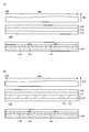
- the schematic sectional view of the light source apparatus which concerns on one Embodiment of this invention. The schematic perspective view of the light source apparatus which concerns on one Embodiment of this invention.
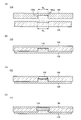
- the schematic sectional view of the light source apparatus which concerns on one Embodiment of this invention. The schematic sectional view of the light source apparatus which concerns on one Embodiment of this invention.
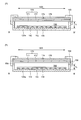
- the schematic perspective view of the light source apparatus which concerns on one Embodiment of this invention The schematic sectional view of the light source apparatus which concerns on one Embodiment of this invention.
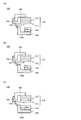
- the schematic perspective view of the light source apparatus which concerns on one Embodiment of this invention A schematic side view and a sectional view of a light source device according to an embodiment of the present invention.
- drawings may schematically represent the width, thickness, shape, etc. of each part as compared with the actual embodiment, but this is merely an example and the interpretation of the present invention is limited. It is not something to do.
- elements having the same functions as those described with respect to the above-described drawings may be designated by the same reference numerals and duplicate description may be omitted.
- the fact that a plurality of elements are integrated means that the plurality of elements have different thicknesses, shapes, directions, etc., and have different functions, but these are formed from one member. To do.
- the integrated elements contain the same material and have the same composition.
- the display device 100 has a light source device 110 and a liquid crystal display module 200 provided so as to overlap the light source device 110 as a basic configuration.
- the display device 100 may include a touch sensor 220 on the liquid crystal display module 200.
- the liquid crystal display module 200 is an array substrate 202, an opposing substrate 214 on the array substrate 202, a pair of polarizing plates 216 and 217 sandwiching the array substrate 202 and the opposing substrate 214, and a liquid crystal sandwiched between the array substrate 202 and the opposing substrate 214. It has a layer (not shown).
- Various patterned conductive films, insulating films, and semiconductor films are laminated on the array substrate 202, and by appropriately arranging these, a drive circuit (scanning line drive circuit) for driving a plurality of pixels 204 or pixels 204. 208, signal line drive circuit 210), a plurality of terminals 212, and the like are formed.
- the display area 206 is formed by the plurality of pixels 204.
- the area other than the display area 206 is called a frame area.
- the pair of polarizing plates 216 and 217 are arranged so as to overlap the display area 206.
- Various signals including video signals and power supplies are supplied to the liquid crystal display module 200 from an external circuit (not shown) via terminals 212, and the drive circuit operates by these signals and power supplies.
- the drive circuit controls the pixel 204, whereby the orientation of the liquid crystal molecules contained in the liquid crystal layer on the pixel 204 is controlled, and the gradation of the light from the light source device 110 is controlled for each pixel.
- the touch sensor 220 having an arbitrary configuration is arranged so as to overlap the display area 206.
- the configuration of the touch sensor 220 is not limited, but as shown in FIG. 1, for example, a capacitance type touch sensor can be used as the touch sensor 220.
- the touch sensor 220 includes a plurality of first touch electrodes 222 extending in one direction (for example, the long side direction of the display area 206), a plurality of second touch electrodes 224 intersecting with the first touch electrode 222, and a plurality of second touch electrodes 224. It is composed of an insulating film (not shown) that electrically insulates them from each other.
- the capacitance is formed by the first touch electrode 222, the second touch electrode 224, and the insulating film, and the capacitance changes when, for example, the user touches the touch sensor 220 with a finger or the like. By detecting this capacitance change, the presence or absence of touch can be determined and the position (coordinates) thereof can be specified, whereby the user can input various commands to the display device 100.
- the light source device 110, the liquid crystal display module 200, and the touch sensor 220 are drawn so as to be separated from each other in FIG. 1, they are fixed to each other by using an adhesive layer, a housing, or the like.
- FIG. 2 shows a schematic development view of the light source device 110.
- the light source device 110 has a rear bezel 120 and a front cover 180 accommodating all or a part of the rear bezel 120, between which the light source substrate 140, the light diffusing plate 170 on the light source substrate 140, and the light diffusing plate 170.
- a prism sheet 174 and a reflective polarizing plate 176 on the prism sheet 174 are arranged.
- a plurality of light emitting diodes 142 are arranged on the light source substrate 140.
- the rear bezel 120 and front cover 180 accommodate a light source substrate 140, a light diffusing plate 170, a prism sheet 174, a reflective polarizing plate 176, and the like that constitute a light source device 110.
- the rear bezel 120 includes lower horizontal plates 120a to 120d, and is between a pair of lower horizontal plates (for example, a pair of lower horizontal plates 120a and 120b and a pair of lower horizontal plates 120c and 120d) facing each other. It has a bottom plate 120e located at. The bottom plate 120e is connected to the lower horizontal plates 120a to 120d. The bottom plate 120e may be integrated with the lower horizontal plates 120a to 120d.
- the lower horizontal plates 120a to 120d are preferably arranged perpendicular to the upper surface of the bottom plate 120e. As a result, the light from the light emitting diode 142 can be efficiently used and supplied to the liquid crystal display module 200.
- the bottom plate 120e of the rear bezel 120 is provided with one or a plurality of openings 120f, and power is supplied to the light emitting diode 142 through the openings 120f.
- the front cover 180 also includes upper horizontal plates 180a to 180d (in FIG. 2, the upper horizontal plate 180b is blocked by the upper plate 180e and is not shown).
- the front cover 180 further has an upper plate 180e located between a pair of upper horizontal plates facing each other (for example, a pair of upper horizontal plates 180a and 180b and a pair of upper horizontal plates 180c and 180d).
- the upper plate 180e is connected to the upper horizontal plates 180a to 180d.
- the upper plate 180e may be integrated with the upper horizontal plates 180a to 180d.
- the upper plate 180e is provided with an opening 180f, and the light from the light emitting diode 142 is supplied to the liquid crystal display module 200 through the opening 180f.
- the upper horizontal plates 180a to 180d are also arranged perpendicular to the upper surface of the upper plate 180e. As a result, not only the light from the light emitting diode 142 can be efficiently used and supplied to the liquid crystal display module 200, but also the area of the frame region can be reduced.
- the rear bezel 120 and the front cover 180 include metals such as aluminum, copper, and stainless steel.
- the rear bezel 120 can be formed by cutting and pressing a metal plate having a thickness of 1 mm or more and 3 mm or less or 1 mm or more and 2 mm or less.
- the thickness of the front cover 180 may be different from that of the rear bezel 120.
- the front cover 180 may be formed by cutting and pressing a metal plate of 0.1 mm or more and 1 mm or less or 0.1 mm or more and 0.5 mm or less.
- the bottom plate 120e and the top plate 180e do not necessarily have to have a flat shape, and may have a curved surface shape.
- the light source substrate 140, the light diffusing plate 170, the prism sheet 174, and the like are also configured to match this curved surface shape.
- FIG. 3 (A) A schematic cross-sectional view of the light source device 110 in the light source substrate and the light emitting diode display area 206 is shown in FIG. 3 (A).
- the light source substrate 140 is housed in the rear bezel 120.
- the light source substrate 140 may be in contact with the rear bezel 120.
- the plurality of light emitting diodes 142 are arranged on the light source substrate 140 and overlap with the display area 206.
- the light emitting diodes 142 can be arranged in a grid pattern, for example, and the spacing (pitch) between the adjacent light emitting diodes 142 can be arbitrarily set according to the size of the display device 100.
- the pitch may be selected from the range of 1 mm or more and 20 mm or less, 3 mm or more and 15 mm or less, or 5 mm or more and 10 mm or less.
- the plurality of light emitting diodes 142 are arranged at a uniform pitch.
- the light emitting diode 142 is an electroluminescent element having an inorganic light emitting body such as gallium nitride or gallium nitride containing indium gallium sandwiched between a pair of electrodes and a protective film for protecting the light emitting element as a basic structure. It is configured to emit light by (Electroluminescence).
- an inorganic compound that gives an emission peak between 400 nm and 530 nm can be selected.
- blue light emission is taken out through the protective film.
- a light emitting diode configured to disperse the color conversion material in the protective film and to mix the light from the inorganic light emitter and the light converted by the color conversion material to give white light emission may be used. Good.
- each light emitting diode 142 there is no limitation on the size of each light emitting diode 142, for example, each occupied area is 1.0 ⁇ 10 4 ⁇ m 2 or more and 1.0 ⁇ 10 6 ⁇ m 2 or less 4.0 ⁇ 10 4 ⁇ m 2 or more 5.0 ⁇ Light emitting diodes of 10 5 ⁇ m 2 or less, or 9.0 ⁇ 10 4 ⁇ m 2 or more and 2.5 ⁇ 10 5 ⁇ m 2 or less can be used. As an example, a so-called micro LED having a size of about 320 ⁇ m ⁇ 300 ⁇ m can be used as the light emitting diode 142.
- the light source device 110 may further have an overcoat 144 that covers the light emitting diode 142.
- the overcoat 144 may be in contact with the light source substrate 140.
- the overcoat 144 has a function of protecting the light emitting diode 142 and preventing the light emitting diode 142 from being separated from the light source substrate 140, and also absorbs unevenness caused by the light emitting diode 142 to give a flat surface. Further, although the light emitting diode 142 gives light having relatively high directivity, the light from the light emitting diode 142 can be spread or diffused by the overcoat 144.
- the overcoat 144 preferably has a high transmittance in the visible light region.
- an acrylic resin, polycarbonate, a polymer material exemplified as polyester such as polyethylene terephthalate, or a silicon-containing inorganic compound such as silicon oxide can be used.
- the thickness of the overcoat 144 can be set arbitrarily, but it is preferably thick enough to cover the light emitting diode 142.
- the thickness may be selected from the range of 200 ⁇ m or more and 1 mm or less, 400 ⁇ m or more and 1 mm or less, or 500 ⁇ m or more and 800 ⁇ m or less.
- the light diffusing plate 170 is provided to diffuse the light from the light emitting diode 142 to give a uniform light emitting surface. More specifically, the light diffusing plate 170 includes a polymer material having a high transmittance for visible light and diffuse particles dispersed in the polymer material. As the polymer material, polycarbonate, polyester, or acrylic resin can be used.
- the diffused particles may be an inorganic compound such as calcium carbonate, barium sulfate, titanium dioxide, aluminum hydroxide, silicon oxide, talc, mica, white carbon, magnesium oxide, or zinc oxide, and may be a polyacrylic acid ester or a polymethacrylic acid ester.
- the thickness of the light diffusing plate 170 can be selected from, for example, 0.5 mm or more and 2 mm or less, or 0.75 mm or more and 1.5 mm or less.
- the light diffusing plate 170 is separated from the light emitting diode 142, and is arranged so that a gap 150 is formed between them.
- the light diffusing plate 170 has a distance (also called an optical distance) from the upper surface of the light source substrate 140 to the bottom surface of the light diffusing plate 170 so that it is 1 mm or more and 3 mm or less, or 1.5 mm or more and 2.5 mm or less. Be placed. Therefore, the light diffusing plate 170 and the light emitting diode 142 do not come into direct contact with each other.
- the structure for separating the light diffusing plate 170 from the light emitting diode 142 will be described later.
- the light diffusing plate 170 may have a laminated structure including a light diffusing layer 171 and a wavelength conversion layer 172.
- the light diffusing layer 171 includes the above-mentioned polymer material having a high transmittance for visible light and diffuse particles dispersed in the polymer material.
- the wavelength conversion layer 172 is a film having a function of converting the wavelength of light emitted from the light emitting diode 142 to generate white light, and has a structure in which phosphors are dispersed in a polymer material.
- the polymer material is selected from materials having high translucency in the visible light region, such as polycarbonate, polyester, and acrylic resin.
- the phosphor contains a fluorescent substance that absorbs blue light emitted from the light emitting diode 142 and emits fluorescence in the green to red region, for example, yellow fluorescence.
- the fluorescent substance include oxides containing yttrium and aluminum.
- the oxide may further contain rare earth metals such as cerium, europium, gadolinium, terbium, lutetium and praseodymium.
- quantum dots instead of the phosphor, quantum dots having a particle size of several nm to several tens of nm may be used.
- the wavelength conversion layer 172 may be laminated with the light diffusion layer 171 as one separately prepared independent film, or a dispersion liquid containing the above-mentioned polymer material or precursor thereof and a phosphor or quantum dots may be laminated as a light diffusion layer. It may be formed by applying it on 171 and then curing it. There are no restrictions on the vertical relationship between the light diffusion layer 171 and the wavelength conversion layer 172, and the light diffusion layer 171 may be located between the light source substrate 140 and the wavelength conversion layer 172 as shown in FIG. 3B, and is not shown. The wavelength conversion layer 172 may be located between the light diffusion layer 171 and the wavelength conversion layer 172.
- the prism sheet 174 is an optical film for efficiently emitting light after passing through the light diffusing plate 170 upward, that is, toward the liquid crystal display module 200 side, and a plurality of prism shapes are arranged in parallel on the surface.
- the prism sheet 174 may have a single-layer structure, or may be formed by laminating two films having a plurality of prism shapes on the surface. In the latter case, the two films may be arranged so that the directions in which the prism shapes are stretched intersect each other.
- the prism sheet 174 can also contain acrylic resin, polycarbonate, polyester, and the like, which are materials having high translucency in the visible light region.
- Reflective polarizing plate The reflective polarizing plate 176 has a function of transmitting polarized light having a polarization axis parallel to the transmission axis of the polarizing plate 216 and reflecting other light among the light transmitted through the prism sheet 174.
- the former is taken out as linearly polarized light from the opening 180f of the front cover 180 and supplied to the liquid crystal display module 200.
- the latter returns to the prism sheet 174 side, and the polarization axis changes by repeating reflection and refraction between the prism sheet 174 and the light source substrate 140.
- the polarized light parallel to the transmission axis of the polarizing plate 216 selectively passes through the reflective polarizing plate 176.
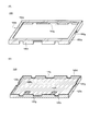
- FIG. 4 is a schematic perspective view including a rear bezel 120, a light source substrate 140, a light diffusing plate 170, and a front cover 180 of the light source device 110 according to the present embodiment, and a schematic side view of the rear bezel 120 and the front cover 180 is shown. It is shown in 5 (A) to 5 (D).
- FIG. 5 (A) shows a state in which the rear bezel 120 and the front cover 180 are separated from each other
- FIGS. 5 (B) to 5 (D) show a state in which the rear bezel 120 is housed in the front cover 180.
- FIGS. 4 and 5 A
- at least one notch 120 g is provided in each of at least a pair of lower horizontal plates facing each other.
- FIG. 4 shows an example in which the rear bezel 120 and the front cover 180 have a rectangular planar shape, and a pair of notches 120 g are provided on the lower horizontal plates (lower horizontal plates 120c and 120d in FIG. 4) forming a long side.
- the notch 120 g may be provided on the lower horizontal plates (lower horizontal plates 120a and 120b in FIG. 4) forming the short side.
- the notch 180g is provided in each of at least a pair of upper horizontal plates facing each other among the upper horizontal plates 180a to 180d. Similar to the notch 120 g, the notch 180 g may be provided on the upper horizontal plates (upper horizontal plates 180a and 180b in FIG. 4) forming the short side. The notch 180 g is provided on the upper horizontal plate corresponding to the lower horizontal plate on which the notch 120 g is provided. For example, when the notch 120 g is provided on the lower horizontal plate forming the long side, the notch 180 g is also provided on the upper horizontal plate forming the long side, and conversely, the notch 120 g is provided on the lower horizontal plate forming the short side.
- a notch of 180 g is also provided on the upper horizontal plate constituting the short side. Further, as shown in FIG. 5B, when the rear bezel 120 is housed in the front cover 180, the notch 120 g and the notch 180 g overlap each other in a direction parallel to the upper surface of the bottom plate 120e. Therefore, in this state, there is a gap 116 between the rear bezel 120 and the front cover 180 on the side surface of the light source device 110.
- the widths W 1 and W 2 of the notches 120 g and 180 g (the lengths of the lower horizontal plate and the upper horizontal plate provided with the notches 120 g and 180 g in the extending direction) can be arbitrarily set.
- the width W 1 and the width W 2 may be the same as each other, and the width W 1 may be larger or smaller than the width W 2 .
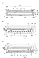
- FIGS. 6 (A) and 6 (B) Schematic diagrams of cross sections along the chain lines AA'and BB' in FIG. 4 are shown in FIGS. 6 (A) and 6 (B), respectively.
- the light diffusing plate 170, the prism sheet 174, the reflective polarizing plate 176, and the like are housed in the front cover 180.
- the reflective polarizing plate 176 is arranged so as to be in contact with the bottom surface of the upper plate 180e of the front cover 180.
- These members are fixed to the front cover 180 by an adhesive tape (hereinafter, simply referred to as an adhesive tape) 152 (FIGS. 6 (A) and 5 (C)). Therefore, the adhesive tape 152 is in contact with the upper horizontal plate provided with the notch 180 g.
- an adhesive tape hereinafter, simply referred to as an adhesive tape
- the adhesive tape 152 may be in contact with the light diffusing layer 171.
- the adhesive tape 152 is provided so as to penetrate the notch 120 g and the notch 180 g. Therefore, the width of the adhesive tape 152 is equal to or less than the smaller width of the width W 1 and the width W 2 .
- the material contained in the support may be a metal such as aluminum or lead, and fibers such as paper, cloth, glass fiber, cellophane, polyimide or polyamide, ethylene-vinyl alcohol copolymer, polyurethane, polyethylene or polypropylene, vinyl chloride, etc.
- Polyester, polyester such as polyethylene terephthalate, synthetic polymer such as polycarbonate and polyether sulfone may be used.
- the pressure-sensitive adhesive include rubber-based adhesives, acrylic-based adhesives, epoxy-based adhesives, silicone-based adhesives, and urethane-based adhesives.
- the thickness of the adhesive tape 152 can be selected from the range of 20 ⁇ m or more and 200 ⁇ m or less, or 50 ⁇ m or more and 100 ⁇ m or less.
- the light source device 110 may further have a light-shielding film 154 covering the adhesive tape 152 (FIGS. 5 (D) and 6 (A)).
- the light-shielding film 154 is provided so as to cover the gap 116 between the rear bezel 120 and the front cover 180 existing on the side surface of the light source device 110.
- the light-shielding film 154 can be provided so as to be in contact with the adhesive tape 152, the rear bezel 120, and the front cover 180. As a result, it is possible to prevent the light from the light emitting diode 142 from leaking to the outside through the gap 116.
- the lower horizontal plates of the rear bezel 120 (here, the lower horizontal plates 120c and 120d) come into contact with the upper plate 180e of the front cover 180. This determines the position of the rear bezel 120 and the front cover 180, and the distance between them. Therefore, the distance between the rear bezel 120 and the front cover 180 and the distance between the light diffusing plate 170 and the light emitting diode 142 are the height of the portion of the lower horizontal plate where the notch 120 g is not formed (perpendicular to the upper surface of the bottom plate 120e).
- the light diffusing plate 170 is separated from the light emitting diode 142, and a gap 150 is formed between them. A part of the adhesive tape 152 exists in the gap 150.
- a cushioning material 156 may be provided on the lower horizontal plate of the rear bezel 120 (FIG. 6 (C)).
- the cushioning material 156 may be formed in a portion where the notch 120 g is not provided.
- the cushioning material 156 preferably contains an elastomer exhibiting rubber elasticity, and as such a material, polysiloxane, polyacrylate, polymethacrylate, polyacrylonitrile, epoxy resin, polybutadiene, polyisoprene, or a copolymer containing these as a basic skeleton. Examples include polymers.
- the light diffusing plate 170, the prism sheet 174, and the reflective polarizing plate 176 do not overlap with the lower horizontal plate of the rear bezel 120. All or part of these members may overlap the lower transverse plate of the rear bezel 120.
- the light diffusing plate 170 may be arranged so as to overlap the lower horizontal plate of the rear bezel 120. Even in this case, the cushioning material 156 can be provided so as to be in contact with the light diffusing plate 170 (FIG. 7B), whereby the light diffusing plate 170 or the like can be prevented from being damaged by the contact with the rear bezel 120. ..
- the lower horizontal plate is configured such that the difference between the height h 1 and the thickness of the light source substrate 140 is 1 mm or more and 3 mm or less, or 1.5 mm or more and 2.5 mm or less.
- the cushioning material 156 is provided, the value obtained by subtracting the thickness of the light source substrate 140 from the sum of the height h 1 and the thickness of the cushioning material 156 is 1 mm or more and 3 mm or less, or 1.5 mm or more. It is configured to be 5 mm or less.
- FIGS. 8 (A) to 8 (C) Enlarged views of the region 130 in FIG. 6 (A) are shown in FIGS. 8 (A) to 8 (C).
- the light source substrate 140 may be arranged so as to be in direct contact with the upper surface of the bottom plate 120e of the rear bezel 120, but may be fixed to the bottom plate 120e using the adhesive layer 160 as shown in FIG. 8A. ..
- the light diffusing plate 170 has a laminated structure of the light diffusing layer 171 and the wavelength conversion layer 172, the light diffusing layer 171 may be in contact with the adhesive tape 152 as shown in FIG. 8 (A), or FIG. 8 (B).
- a wavelength conversion layer 172 may be provided between the light diffusion layer 171 and the light emitting diode 142 so that the adhesive tape 152 is in contact with the wavelength conversion layer 172. Further, the light source substrate 140 may be provided so as to be in contact with the lower horizontal plate of the rear bezel 120 (FIG. 8 (C)).
- the arrangement of the notches 120 g and 180 g can be arbitrarily determined.
- one or more notches 180 g may be arranged on each of the two opposing upper horizontal plates.
- two notches 180 g may be arranged on two opposite upper horizontal plates, one notch 180 g may be arranged on one upper horizontal plate, and two notches 180 g may be arranged on the opposite upper horizontal plate. May be good.
- 180 g of one or a plurality of notches may be formed in all the upper horizontal plates.
- one or more notches 120 g may be arranged on each of the two opposing lower horizontal plates.
- two notches 120 g may be arranged on two opposing lower horizontal plates, one notch 120 g may be arranged on one lower horizontal plate, and two notches 120 g may be arranged on the opposite lower horizontal plate. May be good.
- 120 g of one or more notches may be formed in all the lower horizontal plates.
- the light source substrate 140 on which a plurality of light emitting diodes 142 are arranged is housed in the rear bezel 120, and the light diffusing plate 170, the prism sheet 174, and the reflective polarizing plate 176 are housed and fixed in the front cover 180. Will be done.
- the rear bezel 120 is housed in the front cover 180.
- a liquid crystal display module 200 is arranged on the light source device 110 to form a display device 100.
- a notch 120 g is provided in the lower horizontal plate of the rear bezel 120
- a notch 180 g is also provided in the corresponding upper horizontal plate of the front cover 180.
- the distance between the rear bezel 120 and the front cover 180 can be adjusted by the height h 1 of the lower horizontal plate of the rear bezel 120.
- a gap 150 is formed between the light source substrate 140 and the light diffusing plate 170, and a constant distance is provided between them. Therefore, even if the light emitting diode 142 irradiates light with high directivity, the light spreads in the gap 150 between the light source substrate 140 and the light diffusing plate 170. Further, the directivity is further lowered by repeating the reflection of light in the void 150. As a result, the local generation of a region (hot spot) having high brightness is suppressed on the bottom surface of the light diffusing plate 170.
- the display device 100 enables high-quality display.
- the light emitting diode 142 that functions as a light source can be arranged below the display area 206, that is, under the light diffusing plate 170. Therefore, as compared with the configuration in which the light source is arranged in the frame region, it is not necessary to arrange the reflector for reflecting the light toward the liquid crystal display module 200 side, and the number of parts constituting the light source device can be reduced. This contributes to making the display device thinner. Further, since it is not necessary to arrange the light source in the frame area, the frame area can be reduced and the area of the display area 206 with respect to the entire display device 100 can be increased. Therefore, by applying this embodiment, it is possible to provide a display device having excellent design.
- the light source device 112 including the rear bezel 122 having a structure different from the rear bezel 120 described in the first embodiment, and the display device 102 including the light source device 112 will be described.
- the description of a structure similar to or similar to the structure described in the first embodiment may be omitted.
- the rear bezel 122 of the present embodiment is different from the rear bezel 120 in that it has a spacer 162 along the lower horizontal plate facing the lower horizontal plate provided with the notch 120 g.
- a spacer 162 extending in parallel with the extending direction of the lower horizontal plate 120a is arranged in the rear bezel 122 along the lower horizontal plate 120a facing the lower horizontal plate 120b provided with the notch 120g. Will be done.
- the lower horizontal plate 120a facing the lower horizontal plate 120b provided with the notch 120g may not be provided with the notch.
- the spacer 162 there are no restrictions on the material contained in the spacer 162, and not only polymer materials with high transparency to visible light such as polycarbonate, polyester, and acrylic resin, but also epoxy resin, polyimide resin, polyamide resin, polyolefin resin, and fluorine. Various polymer materials such as the containing polyolefin resin can be used.
- the spacer 162 may be constructed by using a metal or alloy such as aluminum, copper, iron, zinc, brass, or stainless steel.
- the spacer 162 is provided so as to be in contact with the light diffusing plate 170 or to overlap the light diffusing plate 170 via a cushioning material (not shown).
- the spacer 162 is in contact with the wavelength conversion layer 172.
- it is arranged so as to overlap the wavelength conversion layer 172 via a cushioning material.
- the spacer 162 may be separated from the lower horizontal plates (lower horizontal plates 120c and 120d in FIG. 10) extending perpendicularly to the extending direction of the spacer 162, or may be in contact with the lower horizontal plates (not shown).
- the spacer 162 is arranged so that the plurality of light emitting diodes 142 are sandwiched between the lower horizontal plate provided with the notch 120 g and the spacer 162.
- the light diffusing plate 170, the prism sheet 174, the reflective polarizing plate 176, and the like are housed in the front cover 180.
- these members are fixed to the front cover 180 by the adhesive tape 152. That is, in the light source device 112, the light diffusing plate 170, the prism sheet 174, the reflective polarizing plate 176, and the like are fixed by the adhesive tape 152 and the spacer 162.
- the spacer 162 is configured so that the difference between the height h 2 and the thickness of the light source substrate 140 is 1 mm or more and 3 mm or less, or 1.5 mm or more and 2.5 mm or less.
- the lower horizontal plate has a value obtained by subtracting the thickness of the light diffusing plate 170, the prism sheet 174, the reflective polarizing plate 176, and the light source substrate 140 from the height h 1 of 1 mm or more and 3 mm or less, or 1.5 mm or more 2 It is configured to be 5.5 mm or less.
- the light diffusing plate 170, the prism sheet 174, and the reflective polarizing plate 176 may or may not be in contact with the lower horizontal plate 120a facing the lower horizontal plate 120b provided with the notch 120g.
- a cushioning material 158 may be provided between the lower horizontal plate facing the lower horizontal plate provided with the notch 120 g and the light diffusing plate 170, the prism sheet 174, and the reflective polarizing plate 176.
- the cushioning material 158 is arranged on the spacer 162. This makes it possible to prevent members such as the light diffusing plate 170 from coming into contact with the rear bezel 122 and being damaged.
- the cushioning material 158 can include materials that can be used in the cushioning material 156 described in the first embodiment.
- the spacer 162 may be arranged on the light source substrate 140 so as to overlap the light source substrate 140. Also in this case, the plurality of light emitting diodes 142 are sandwiched between the lower horizontal plate provided with the notch 120 g and the spacer 162.
- the height h 2 of the spacer 162 (the sum of the thickness and the height h 2 when the overcoat 144 is provided) is 1 mm or more and 3 mm or less, or 1.5 mm or more and 2.5 mm or less. It is composed.
- the lower horizontal plate has the thickness of the light diffusing plate 170, the prism sheet 174, the reflective polarizing plate 176, and the light source substrate 140 from the height h 1 (the sum of the thicknesses when the overcoat 144 is provided). Is configured so that the value obtained by subtracting is 1 mm or more and 3 mm or less, or 1.5 mm or more and 2.5 mm or less.
- the liquid crystal display module 200 is formed with a terminal 212 for supplying various signals and power from the outside, and a connector 218 such as a flexible printed circuit (FPC) board is connected to the terminal 212 (FIG. 1. See FIG. 11 (B)).
- a connector 218 such as a flexible printed circuit (FPC) board is connected to the terminal 212 (FIG. 1. See FIG. 11 (B)).
- the frame area on the terminal 212 side is wider than the frame area on the opposite side of the terminal 212. Therefore, it is preferable to form a notch 120 g on the side opposite to the terminal 212 of the liquid crystal display module 200 and arrange the spacer 162 on the terminal 212 side. This makes it possible to effectively utilize a relatively large frame area for the placement of the spacer 162.
- the notch 120 g is provided on one of the lower horizontal plates (lower horizontal plate 120c or 120d in FIG. 10) forming the long side of the rear bezel 122. It is preferable to provide a notch 120 g and a spacer 162 on the lower horizontal plate side facing the notch.
- the position of the light diffusing plate 170 is fixed by the adhesive tape 152 penetrating the notch 120 g and the spacer 162, and a gap 150 for separating the light diffusing plate 170 from the light emitting diode 142 can be formed. .. Therefore, the light from the light emitting diode 142 having high directivity is effectively diffused by the light diffusing ability of the void 150 and the light diffusing plate 170, and the light having uniform brightness can be incident on the prism sheet 174. As a result, light having uniform brightness is provided for the display area 206, and the display device 102 enables high-quality display.
- a light source device 114 having a rear bezel 124 having a structure different from the rear bezels 120 and 122 described in the first and second embodiments, and a display device 104 including the light source device 114 will be described.
- the description of a structure similar to or similar to the structure described in the first and second embodiments may be omitted.
- FIGS. 12 (A) and 12 (B) A schematic perspective view of the light source device 114 is shown in FIGS. 12 (A) and 12 (B).
- 13 (A) is a schematic side view of the rear bezel 124
- FIGS. 13 (B) and 13 (C) are schematic cross sections along the chain lines EE and FF'of FIG. 12 (B).
- FIG. 12A shows a state before the light diffusing plate 170, the prism sheet 174, the reflective polarizing plate 176, and the like are housed in the rear bezel 124
- FIG. 12B shows a state in which these members are housed in the rear bezel 124. Represents.
- hatching is not applied to the bottom plate 120e and the surface parallel to the upper surface thereof in consideration of visibility.
- one lower horizontal plate (here, the lower horizontal plate 120a) of the rear bezel 124 is provided with an opening 120h.
- the opening 120h is formed so as to penetrate the light diffusing plate 170, the prism sheet 174, and the reflective polarizing plate 176.
- the opening 120h is formed such that its height h 3 (bottom plate upper surface to the length of the direction perpendicular 120e) the light diffusion plate 170, a prism sheet 174, and greater than or equal to the sum of the thickness of the reflective polarizer 176
- the width W 3 (the length in the direction in which the lower horizontal plate provided with the opening 120h is extended) is formed so as to be equal to or larger than the maximum width of the light diffusing plate 170, the prism sheet 174, and the reflective polarizing plate 176. Will be done.
- the inner surface of the lower horizontal plate (here, the lower horizontal plates 120c and 120d) where the extension direction intersects with the lower horizontal plate provided with the opening 120h ,
- a pair of protruding portions 120j extending parallel to the upper surface of the bottom plate 120e are formed.
- the protruding portion 120j closer to the bottom plate 120e is also referred to as a lower guide
- the other protruding portion 120j is also referred to as an upper guide.
- the protruding portion 120j projects toward the facing lower horizontal plate.
- the pair of protrusions 120j form grooves extending parallel to the upper surface of the bottom plate 120e on each of the lower horizontal plates facing each other.
- the width of the groove that is, the gap g 1 between the pair of protruding portions 120j (the length of the groove in the direction perpendicular to the upper surface of the bottom plate 120e) is the light diffusing plate 170, the prism sheet 174, and the reflective polarizing plate. It is provided so as to be equal to or greater than the sum of the thicknesses of 176.
- the gap g 1 may be the same as the height h 3 .
- the lower guide height h 4 i.e., in a direction perpendicular to the upper surface of the bottom plate 120e, the distance from the upper surface of the bottom plate 120e to the upper surface of the lower guide, the same as the distance from the upper surface of the bottom plate 120e to the opening 120h , Or substantially the same.
- the protrusion 120j and the opening 120h are formed so that the difference between the height h 4 and the thickness of the light source substrate 140 is 1 mm or more and 3 mm or less, or 1.5 mm or more and 2.5 mm or less. Therefore, the groove and the opening 120h overlap each other in the side view.
- a pair of protrusions 120j may also be formed on the lower horizontal plate (here, the lower horizontal plate 120b) facing the lower horizontal plate provided with the opening 120h (FIG. 13 (C)), or may not be provided (FIG. 13C). FIG. 13 (D).
- the bottom plate 120e and the lower horizontal plates 120a to 120d do not necessarily have to be integrated, and all or part of them may be independent structures. In this case, the bottom plate 120e and the lower horizontal plates 120a to 120d are connected and fixed to each other by welding, screwing, or by using an adhesive or adhesive tape.
- the light diffusing plate 170, the prism sheet 174, and the reflective polarizing plate 176 can be inserted into the rear bezel 124 from the opening 120h along a pair of grooves, and these members can be fixed. (FIG. 12 (B), FIG. 13 (B)). Therefore, both ends of the light diffusing plate 170, the prism sheet 174, and the reflective polarizing plate 176 are located in the groove and are sandwiched between the pair of protruding portions 120j.
- a pair of projecting portions 120j are also provided on the lower horizontal plate facing the lower horizontal plate provided with the opening 120h, the light diffusing plate 170, the prism sheet 174, and the reflective polarizing plate are provided in the grooves formed in the lower horizontal plate.
- the light source device 114 may include a light-shielding film 154 that covers the opening 120h and the light diffusing plate 170 inserted in the rear bezel 124 (FIGS. 13 (C) and 13 (D)). This makes it possible to prevent the light from the light emitting diode 142 from leaking to the outside from the opening 120h or the side surface of the light diffusing plate 170.
- a gap 150 is formed between the plurality of light emitting diodes 142 and the light diffusing plate 170 by the grooves formed by the pair of protruding portions 120j, and the distance between the light emitting diode 142 and the light diffusing plate 170 is on the lower side. It can be controlled by the height h 4 of the guide. Therefore, as described in the first and second embodiments, the light from the light emitting diode 142 is effectively diffused, and the light having uniform brightness can be incident on the prism sheet 174. As a result, light having uniform brightness is provided for the display area 206, and the display device 104 enables high-quality display.
- the light diffusing plate 170, the prism sheet 174, and the reflective polarizing plate 176 are inserted into the rear bezel 124. Therefore, in the form, it is not necessary to install the front cover 180.
- the configuration of the light source device 114 of the present embodiment is not limited to this, and a part of the light diffusing plate 170, the prism sheet 174, and the reflective polarizing plate 176 is inserted and fixed in the rear bezel 124, and other members. May be provided between the rear bezel 124 and the front cover 180.
- the rear bezel 124 can be configured to do so.
- the opening 120h is provided so that its height h 3 and width W 3 are equal to or larger than the thickness and width of the light diffusing plate 170, respectively.
- the pair of projecting portions 120j are also provided so that the gap g 1 is equal to or larger than the thickness of the light diffusing plate 170.
- a front cover 180 for accommodating the rear bezel 124 is provided on the rear bezel 124, and a prism sheet 174, a reflective polarizing plate 176, and the like are sandwiched between them.
- the light source device 114 may be configured so that only the light diffusing plate 170 and the prism sheet 174 are inserted into the rear bezel 124.
Landscapes
- Physics & Mathematics (AREA)
- General Physics & Mathematics (AREA)
- Optics & Photonics (AREA)
- Nonlinear Science (AREA)
- Engineering & Computer Science (AREA)
- General Engineering & Computer Science (AREA)
- Mathematical Physics (AREA)
- Chemical & Material Sciences (AREA)
- Crystallography & Structural Chemistry (AREA)
- Planar Illumination Modules (AREA)
- Liquid Crystal (AREA)
- Fastening Of Light Sources Or Lamp Holders (AREA)
Abstract
光源装置はリアベゼル、光源基板、発光ダイオード、フロントカバー、および光拡散板を備える。リアベゼルは底板、および底板に接続された第1の下横板を有する。光源基板はリアベゼル内に収容される。複数の発光ダイオードは光源基板上に位置する。フロントカバーは上板、および上板に接続された第1の上横板を有し、リアベゼル上に位置し、リアベゼルを収容する。光拡散板はフロントカバー内に収容され、複数の発光ダイオード上に位置し、複数の発光ダイオードから離隔する。第1の下横板と第1の上横板は、いずれも切り欠きを有する。
Description
本発明の実施形態は液晶モジュール用光源装置、および光源装置を備える表示装置に関する。
現在最も汎用されている表示装置の一つとして液晶表示装置が挙げられる。液晶表示装置は、光源装置(バックライト)、光源装置上に配置される液晶表示モジュールを基本構成として有している。光源装置の光源としては、冷陰極管や無機化合物を発光体として含む発光ダイオード(LED)が用いられる。例えば特許文献1から3では、複数の発光ダイオードが液晶表示モジュールと重なるように配置された光源装置を備える液晶表示装置が開示されている。
本発明に係る実施形態の一つは、液晶表示モジュールを均一な輝度で光照射可能な光源装置、およびこれを備える表示装置を提供することを課題の一つとする。あるいは実施形態の一つは、額縁領域が狭く、デザイン性の高い液晶表示装置を提供することを課題の一つとする。
本発明の実施形態の一つは光源装置である。この光源装置はリアベゼル、光源基板、複数の発光ダイオード、フロントカバー、および光拡散板を備える。リアベゼルは底板、および底板に接続された第1の下横板を有する。光源基板はリアベゼル内に収容される。複数の発光ダイオードは光源基板上に位置する。フロントカバーは上板、および上板に接続された第1の上横板を有し、リアベゼル上に位置し、リアベゼルを収容する。光拡散板はフロントカバー内に収容され、複数の発光ダイオード上に位置し、複数の発光ダイオードから離隔する。第1の下横板と第1の上横板は、いずれも切り欠きを有する。
本発明の実施形態の一つは光源装置である。この光源装置はリアベゼル、光源基板、複数の発光ダイオード、および光拡散板を備える。リアベゼルは第1の横板、第1の横板に対向する第2の横板、第1の横板と第2の横板に接続された底板を有する。光源基板はリアベゼル内に収容される。複数の発光ダイオードは光源基板上に位置する。光拡散板はリアベゼル内に収容され、複数の発光ダイオード上に位置し、複数の発光ダイオードと重なり、複数の発光ダイオードから離隔される。第1の横板と第2の横板はいずれも、底板に平行な方向に延伸する下側ガイドと上側ガイドを有する。光拡散板の互いに対向する端部は、下側ガイドと上側ガイドによって形成される溝内に位置する。
本発明の実施形態の一つは表示装置である。この表示装置は光源装置、および光源装置上の液晶表示モジュールを備える。光源装置はリアベゼル、光源基板、複数の発光ダイオード、フロントカバー、光拡散板、および接着テープを備える。リアベゼルは底板、および底板に接続された第1の下横板を有する。光源基板はリアベゼル内に収容される。複数の発光ダイオードは光源基板上に位置する。フロントカバーは上板、および上板に接続された第1の上横板を有し、リアベゼル上に位置し、リアベゼルを収容する。光拡散板はフロントカバー内に収容され、複数の発光ダイオード上に位置し、複数の発光ダイオードから離隔する。接着テープは光拡散板をフロントカバーに固定する。第1の下横板と第1の上横板は、いずれも切り欠きを有する。接着テープはリアベゼルとフロントカバーに挟まれ、第1の上横板の切り欠きと第1の下横板の切り欠きを貫通する。
本発明の実施形態の一つは表示装置である。この表示装置は光源装置、および光源装置上の液晶表示モジュールを備える。光源装置はリアベゼル、光源基板、複数の発光ダイオード、および光拡散板を備える。リアベゼルは第1の横板、第1の横板に対向する第2の横板、第1の横板と第2の横板に接続された底板を有する。光源基板はリアベゼル内に収容される。複数の発光ダイオードは光源基板上に位置する。光拡散板はリアベゼル内に収容され、複数の発光ダイオード上に位置し、複数の発光ダイオードと重なり、複数の発光ダイオードから離隔される。第1の横板と第2の横板はいずれも、底板に平行な方向に延伸する下側ガイドと上側ガイドを有する。光拡散板の互いに対向する端部は、下側ガイドと上側ガイドによって形成される溝内に位置する。
以下、本発明の各実施形態について、図面等を参照しつつ説明する。但し、本発明は、その要旨を逸脱しない範囲において様々な態様で実施することができ、以下に例示する実施形態の記載内容に限定して解釈されるものではない。
図面は、説明をより明確にするため、実際の態様に比べ、各部の幅、厚さ、形状等について模式的に表される場合があるが、あくまで一例であって、本発明の解釈を限定するものではない。本明細書と各図において、既出の図に関して説明したものと同様の機能を備えた要素には、同一の符号を付して、重複する説明を省略することがある。
本明細書および請求項において、ある構造体の上に他の構造体を配置する態様を表現するにあたり、単に「上に」と表記する場合、特に断りの無い限りは、ある構造体に接するように、直上に他の構造体を配置する場合と、ある構造体の上方に、さらに別の構造体を介して他の構造体を配置する場合との両方を含むものとする。
本明細書および請求項において、複数の要素が一体化されるとは、複数の要素は互いに厚さや形状、方向などが異なり異なる機能を有するが、これらは一つの部材から形成されることを意味する。したがって一体化された複数の要素は、互いに同一の材料を含み、同一の組成を有する。
<第1実施形態>
本実施形態では、本発明の実施形態の一つに係る光源装置110、および光源装置110を備える表示装置100について説明する。
本実施形態では、本発明の実施形態の一つに係る光源装置110、および光源装置110を備える表示装置100について説明する。
1.全体構成
表示装置100の全体構成を図1の模式的な展開図を用いて説明する。表示装置100は光源装置110、および光源装置110と重なるように設けられる液晶表示モジュール200を基本的な構成として有する。任意の構成として、表示装置100は液晶表示モジュール200上のタッチセンサ220を備えてもよい。
表示装置100の全体構成を図1の模式的な展開図を用いて説明する。表示装置100は光源装置110、および光源装置110と重なるように設けられる液晶表示モジュール200を基本的な構成として有する。任意の構成として、表示装置100は液晶表示モジュール200上のタッチセンサ220を備えてもよい。
液晶表示モジュール200はアレイ基板202、アレイ基板202上の対向基板214、アレイ基板202と対向基板214を挟持する一対の偏光板216、217、およびアレイ基板202と対向基板214の間に挟まれる液晶層(図示しない)を有する。アレイ基板202上にはパターニングされた種々の導電膜、絶縁膜、半導体膜が積層され、これらが適宜配置されることで複数の画素204や画素204を駆動するための駆動回路(走査線駆動回路208、信号線駆動回路210)、複数の端子212などが形成される。複数の画素204によって表示領域206が形成される。表示領域206以外の領域は額縁領域と呼ばれる。
一対の偏光板216、217は表示領域206と重なるように配置される。端子212を介して外部回路(図示しない)から映像信号を含む種々の信号、および電源が液晶表示モジュール200に供給され、これらの信号や電源によって駆動回路が動作する。駆動回路は画素204を制御し、これによって画素204上の液晶層に含まれる液晶分子の配向が制御され、光源装置110からの光の階調が画素ごとに制御される。
任意の構成であるタッチセンサ220は、表示領域206と重なるように配置される。タッチセンサ220の構成に制限はないが、図1に示すように、例えば静電容量方式のタッチセンサをタッチセンサ220として用いることができる。この場合タッチセンサ220は、一方向(例えば表示領域206の長辺方向)に延伸する複数の第1のタッチ電極222、第1のタッチ電極222と交差する複数の第2のタッチ電極224、およびこれらを互いに電気的に絶縁する絶縁膜(図示しない)によって構成される。第1のタッチ電極222、第2のタッチ電極224、および絶縁膜によって容量が形成され、たとえばユーザが指などでタッチセンサ220をタッチした際に容量が変化する。この容量変化を検出することでタッチの有無を判断し、かつ、その位置(座標)を特定することができ、これによりユーザは種々の命令を表示装置100に対して入力することができる。なお、図1では光源装置110や液晶表示モジュール200、タッチセンサ220は離隔するように描かれているが、これらは互いに接着層や筐体などを用いて固定される。
2.光源装置
図2に光源装置110の模式的な展開図を示す。光源装置110は、リアベゼル120、およびリアベゼル120の全てまたは一部を収容するフロントカバー180を有し、これらの間に光源基板140、光源基板140上の光拡散板170、光拡散板170上のプリズムシート174、およびプリズムシート174上の反射型偏光板176が配置される。光源基板140上には複数の発光ダイオード142が配置される。
図2に光源装置110の模式的な展開図を示す。光源装置110は、リアベゼル120、およびリアベゼル120の全てまたは一部を収容するフロントカバー180を有し、これらの間に光源基板140、光源基板140上の光拡散板170、光拡散板170上のプリズムシート174、およびプリズムシート174上の反射型偏光板176が配置される。光源基板140上には複数の発光ダイオード142が配置される。
2-1.リアベゼルとフロントカバー
リアベゼル120とフロントカバー180は、光源装置110を構成する光源基板140や光拡散板170、プリズムシート174、反射型偏光板176などを収容する。図2に示すように、リアベゼル120は下横板120aから120dを備え、さらに互いに対向する一対の下横板(例えば下横板120aと120bの対、下横板120cと120dの対)の間に位置する底板120eを有する。底板120eは下横板120aから120dと接続されている。底板120eは下横板120aから120dと一体化されていてもよい。下横板120aから120dは底板120eの上面に対して垂直に配置することが好ましい。これにより、発光ダイオード142からの光を効率よく利用して液晶表示モジュール200に供給することができる。リアベゼル120の底板120eには一つ、あるいは複数の開口120fが設けられ、この開口120fを介して発光ダイオード142へ電源が供給される。
リアベゼル120とフロントカバー180は、光源装置110を構成する光源基板140や光拡散板170、プリズムシート174、反射型偏光板176などを収容する。図2に示すように、リアベゼル120は下横板120aから120dを備え、さらに互いに対向する一対の下横板(例えば下横板120aと120bの対、下横板120cと120dの対)の間に位置する底板120eを有する。底板120eは下横板120aから120dと接続されている。底板120eは下横板120aから120dと一体化されていてもよい。下横板120aから120dは底板120eの上面に対して垂直に配置することが好ましい。これにより、発光ダイオード142からの光を効率よく利用して液晶表示モジュール200に供給することができる。リアベゼル120の底板120eには一つ、あるいは複数の開口120fが設けられ、この開口120fを介して発光ダイオード142へ電源が供給される。
図2に示すように、フロントカバー180も同様に上横板180aから180dを備える(図2では、上横板180bは上板180eに遮られるため、図示されない)。フロントカバー180はさらに、互いに対向する一対の上横板(例えば上横板180aと180bの対、上横板180cと180dの対)の間に位置する上板180eを有する。上板180eは上横板180aから180dと接続される。上板180eは上横板180aから180dと一体化されていてもよい。上板180eには開口180fが設けられ、この開口180fを介して発光ダイオード142からの光が液晶表示モジュール200へ供給される。上横板180aから180dも上板180eの上面に対して垂直に配置することが好ましい。これにより、発光ダイオード142からの光を効率よく利用して液晶表示モジュール200に供給することができるだけでなく、額縁領域の面積を小さくすることができる。
リアベゼル120とフロントカバー180は、アルミニウムや銅、ステンレスなどの金属を含む。例えば厚さが1mm以上3mm以下あるいは1mm以上2mm以下の金属プレートを切削加工、プレス加工することでリアベゼル120を形成することができる。フロントカバー180の厚さはリアベゼル120のそれと異なってもよい。例えば0.1mm以上1mm以下あるいは0.1mm以上0.5mm以下の金属板を切削加工、プレス加工することでフロントカバー180を形成すればよい。
なお、底板120e、上板180eは必ずしも平坦な形状を有する必要は無く、曲面形状を有していてもよい。この場合、光源基板140や光拡散板170、プリズムシート174などもこの曲面形状に合致するように構成される。
2-2.光源基板と発光ダイオード
表示領域206における光源装置110の模式的断面図を図3(A)に示す。上述したように光源基板140はリアベゼル120内に収容される。光源基板140はリアベゼル120と接してもよい。
表示領域206における光源装置110の模式的断面図を図3(A)に示す。上述したように光源基板140はリアベゼル120内に収容される。光源基板140はリアベゼル120と接してもよい。
複数の発光ダイオード142は光源基板140の上に配置され、表示領域206と重なる。発光ダイオード142は例えば格子状に配置することができ、隣接する発光ダイオード142の間隔(ピッチ)も表示装置100の大きさによって任意に設定することができる。例えばピッチは1mm以上20mm以下、3mm以上15mm以下、あるいは5mm以上10mm以下の範囲から選択すればよい。表示領域206にわたって均一な輝度の光を供給するため、複数の発光ダイオード142は均等なピッチで配置されることが好ましい。
発光ダイオード142は、窒化ガリウム、インジウムを含む窒化ガリウムなどの無機発光体を一対の電極で挟持した発光素子、および発光素子を保護する保護膜を基本的な構造として有する発光素子であり、電界発光(Electroluminescence)によって発光するように構成される。無機発光体としては、例えば400nmから530nmの間に発光ピークを与える無機化合物を選択することができる。このような発光ダイオード142では、青色の発光が保護膜を介して取り出される。あるいは保護膜中に色変換材料を分散させ、無機発光体からの光と色変換材料によってこの光が変換された光が混合されて白色の発光を与えるように構成された発光ダイオードを用いてもよい。
各発光ダイオード142の大きさに制約はなく、例えばそれぞれの占有面積が1.0×104μm2以上1.0×106μm2以下、4.0×104μm2以上5.0×105μm2以下、あるいは9.0×104μm2以上2.5×105μm2以下の発光ダイオードを用いることができる。一例として大きさが320μm×300μm程度の所謂マイクロLEDを発光ダイオード142として用いることができる。
光源装置110はさらに、発光ダイオード142を覆うオーバーコート144を有してもよい。オーバーコート144は光源基板140と接してもよい。オーバーコート144は発光ダイオード142を保護し、光源基板140から分離することを防ぐ機能を有するとともに、発光ダイオード142に起因する凹凸を吸収して平坦な表面を与える。また、発光ダイオード142は比較的指向性の高い光を与えるが、オーバーコート144により発光ダイオード142からの光を広げる、あるいは拡散させることができる。
オーバーコート144は可視光領域の透過率が高いことが好ましく、例えばアクリル系樹脂やポリカルボナート、あるいはポリエチレンテレフタレートなどのポリエステルに例示される高分子材料、あるいは酸化ケイ素などのケイ素含有無機化合物などを含むように形成される。オーバーコート144の厚さは任意に設定することができるが、発光ダイオード142を覆う程度の厚さが好ましい。例えばその厚さは、200μm以上1mm以下、400μm以上1mm以下、あるいは500μm以上800μm以下の範囲から選択すればよい。
2-3.光拡散板
光拡散板170は、発光ダイオード142からの光を拡散し、均一な発光面を与えるために設けられる。より具体的には、光拡散板170は可視光に対する透過率が高い高分子材料、およびこの高分子材料中に分散した拡散粒子を含む。高分子材料としては、ポリカルボナートやポリエステル、あるいはアクリル系樹脂を用いることができる。拡散粒子としては、炭酸カルシウム、硫酸バリウム、二酸化チタン、水酸化アルミニウム、酸化ケイ素、タルク、マイカ、ホワイトカーボン、酸化マグネシウム、あるいは酸化亜鉛などの無機化合物でも良く、ポリアクリル酸エステル、ポリメタクリル酸エステル、ポリスチレンなどを基本骨格として有する高分子材料でも良い。光拡散板170の厚さは、例えば0.5mm以上2mm以下、あるいは0.75mm以上1.5mm以下の範囲から選択することができる。光拡散板170を配置することで指向性の高い発光ダイオード142からの光が効果的に拡散され、光拡散板170が配置される面内における輝度の分布が低下する。その結果、プリズムシート174に対して均一な輝度で光を提供することができる。
光拡散板170は、発光ダイオード142からの光を拡散し、均一な発光面を与えるために設けられる。より具体的には、光拡散板170は可視光に対する透過率が高い高分子材料、およびこの高分子材料中に分散した拡散粒子を含む。高分子材料としては、ポリカルボナートやポリエステル、あるいはアクリル系樹脂を用いることができる。拡散粒子としては、炭酸カルシウム、硫酸バリウム、二酸化チタン、水酸化アルミニウム、酸化ケイ素、タルク、マイカ、ホワイトカーボン、酸化マグネシウム、あるいは酸化亜鉛などの無機化合物でも良く、ポリアクリル酸エステル、ポリメタクリル酸エステル、ポリスチレンなどを基本骨格として有する高分子材料でも良い。光拡散板170の厚さは、例えば0.5mm以上2mm以下、あるいは0.75mm以上1.5mm以下の範囲から選択することができる。光拡散板170を配置することで指向性の高い発光ダイオード142からの光が効果的に拡散され、光拡散板170が配置される面内における輝度の分布が低下する。その結果、プリズムシート174に対して均一な輝度で光を提供することができる。
ここで、光拡散板170は発光ダイオード142から離隔される、これらの間に空隙150が形成されるように配置される。具体的には、光源基板140の上面から光拡散板170の底面までの距離(光学距離とも呼ばれる)が1mm以上3mm以下、あるいは1.5mm以上2.5mm以下となるように光拡散板170が配置される。したがって、光拡散板170と発光ダイオード142は直接接しない。光拡散板170を発光ダイオード142から離隔させるための構造については後述する。
任意の構成として、図3(B)に示すように、光拡散板170は光拡散層171と波長変換層172を含む積層構造を有してもよい。光拡散層171は上述した可視光に対する透過率が高い高分子材料、およびこの高分子材料中に分散した拡散粒子を含む。一方、波長変換層172は発光ダイオード142から出射した光の波長を変換して白色光を生成する機能を有する膜であり、高分子材料中に蛍光体が分散した構造を有する。光拡散層171と同様、高分子材料はポリカルボナートやポリエステル、アクリル樹脂などの可視光領域の透光性が高い材料から選択される。蛍光体は、発光ダイオード142から射出される青色の光を吸収し、緑から赤色の領域の蛍光、例えば黄色の蛍光を発する蛍光物質を含む。蛍光物質としては、例えばイットリウムとアルミニウムを含む酸化物が例示される。この酸化物には、セリウムやユーロピウム、ガドリニウム、テルビウム、ルテチウム、プラセオジムなどの希土類金属がさらに含まれていてもよい。あるいは、蛍光体に替わり、粒径が数nmから数十nmの量子ドットを用いてもよい。
波長変換層172は、別途作製した一つの独立膜として光拡散層171と積層してもよく、あるいは上述した高分子材料またはその前駆体、および蛍光体または量子ドットを含む分散液を光拡散層171の上に塗布し、その後硬化することで形成してもよい。光拡散層171と波長変換層172の上下関係に制約はなく、図3(B)に示すように光拡散層171が光源基板140と波長変換層172の間に位置してもよく、図示しないが波長変換層172が光拡散層171と波長変換層172の間に位置してもよい。
2-4.プリズムシート
プリズムシート174は、光拡散板170を通過した後の光を上方向、すなわち液晶表示モジュール200側へ効率よく出射させるための光学フィルムであり、表面に複数のプリズム形状が平行に配置された構造を有する。プリズムシート174は単層構造を有していてもよく、あるいは表面に複数のプリズム形状を有するフィルムを二枚積層して構成してもよい。後者の場合、プリズム形状が延伸する方向が互いに交差するように二枚のフィルムを配置すればよい。プリズムシート174も可視光領域の透光性が高い材料であるアクリル樹脂やポリカルボナート、ポリエステルなどを含むことができる。
プリズムシート174は、光拡散板170を通過した後の光を上方向、すなわち液晶表示モジュール200側へ効率よく出射させるための光学フィルムであり、表面に複数のプリズム形状が平行に配置された構造を有する。プリズムシート174は単層構造を有していてもよく、あるいは表面に複数のプリズム形状を有するフィルムを二枚積層して構成してもよい。後者の場合、プリズム形状が延伸する方向が互いに交差するように二枚のフィルムを配置すればよい。プリズムシート174も可視光領域の透光性が高い材料であるアクリル樹脂やポリカルボナート、ポリエステルなどを含むことができる。
2-5.反射型偏光板
反射型偏光板176はプリズムシート174を透過した光のうち、偏光板216の透過軸に平行な偏光軸を有する偏光を透過し、それ以外の光を反射する機能を有する。前者はフロントカバー180の開口180fから直線偏光として取り出されて液晶表示モジュール200へ供給される。一方、後者はプリズムシート174側へ戻り、プリズムシート174から光源基板140の間で反射・屈折を繰り返すことで偏光軸が変化する。偏光軸が変化した光が再び反射型偏光板176に達すると、偏光板216の透過軸に平行な偏光が選択的に反射型偏光板176を透過する。これを繰り返すことで、発光ダイオード142からの光の大部分を液晶表示モジュール200へ供給することができ、表示装置100の消費電力を低減することができる。
反射型偏光板176はプリズムシート174を透過した光のうち、偏光板216の透過軸に平行な偏光軸を有する偏光を透過し、それ以外の光を反射する機能を有する。前者はフロントカバー180の開口180fから直線偏光として取り出されて液晶表示モジュール200へ供給される。一方、後者はプリズムシート174側へ戻り、プリズムシート174から光源基板140の間で反射・屈折を繰り返すことで偏光軸が変化する。偏光軸が変化した光が再び反射型偏光板176に達すると、偏光板216の透過軸に平行な偏光が選択的に反射型偏光板176を透過する。これを繰り返すことで、発光ダイオード142からの光の大部分を液晶表示モジュール200へ供給することができ、表示装置100の消費電力を低減することができる。
3.光拡散板の配置と発光ダイオードとの離隔
上述したように光源装置110では、光拡散板170は発光ダイオード142から離隔し、これらの間に空隙150が形成されるように配置される。本実施形態では、このための構造がリアベゼル120とフロントカバー180に構築される。本実施形態に係る光源装置110のリアベゼル120、光源基板140、光拡散板170、およびフロントカバー180を含む模式的な斜視図を図4に、リアベゼル120とフロントカバー180の模式的側面図を図5(A)から図5(D)に示す。図5(A)はリアベゼル120とフロントカバー180が離隔した状態を示し、図5(B)から図5(D)はリアベゼル120がフロントカバー180内に収容された状態を表す。
上述したように光源装置110では、光拡散板170は発光ダイオード142から離隔し、これらの間に空隙150が形成されるように配置される。本実施形態では、このための構造がリアベゼル120とフロントカバー180に構築される。本実施形態に係る光源装置110のリアベゼル120、光源基板140、光拡散板170、およびフロントカバー180を含む模式的な斜視図を図4に、リアベゼル120とフロントカバー180の模式的側面図を図5(A)から図5(D)に示す。図5(A)はリアベゼル120とフロントカバー180が離隔した状態を示し、図5(B)から図5(D)はリアベゼル120がフロントカバー180内に収容された状態を表す。
図4、図5(A)に示すように、リアベゼル120では、互いに対向する少なくとも一対の下横板のそれぞれに少なくとも一つの切り欠き120gが設けられる。図4ではリアベゼル120とフロントカバー180が長方形の平面形状を有し、一対の切り欠き120gが長辺を構成する下横板(図4では下横板120cと120d)に設けられる例が示されているが、切り欠き120gは短辺を構成する下横板(図4では下横板120aと120b)に設けられていてもよい。
同様に、フロントカバー180では、上横板180aから180dのうち互いに対向する少なくとも一対の上横板のそれぞれに少なくとも一つの切り欠き180gが設けられる。切り欠き120gと同様、切り欠き180gも短辺を構成する上横板(図4では上横板180aと180b)に設けられていてもよい。切り欠き180gは、切り欠き120gが設けられる下横板に対応する上横板に設けられる。例えば切り欠き120gが長辺を構成する下横板に設けられる場合には切り欠き180gも長辺を構成する上横板に設けられ、逆に切り欠き120gが短辺を構成する下横板に設けられる場合には切り欠き180gも短辺を構成する上横板に設けられる。また、図5(B)に示すように、リアベゼル120がフロントカバー180内に収容された状態では、切り欠き120gと切り欠き180gは、底板120eの上面に平行な方向において互いに重なる。したがってこの状態では、光源装置110の側面には、リアベゼル120とフロントカバー180の間にギャップ116が存在する。切り欠き120g、180gの幅(切り欠き120g、180gが設けられる下横板、上横板が延伸する方向の長さ)W1、W2は任意に設定することができる。幅W1、幅W2は互いに同一でも良く、幅W1が幅W2よりも大きくても小さくてもよい。
図4の鎖線A-A´、B-B´に沿った断面の模式図をそれぞれ図6(A)、図6(B)に示す。図6(A)に示すように、光拡散板170やプリズムシート174、および反射型偏光板176などはフロントカバー180内に収容される。反射型偏光板176はフロントカバー180の上板180eの底面と接するように配置される。これらの部材は、接着性を有するテープ(以下、単に接着テープと記す)152によってフロントカバー180に固定される(図6(A)、図5(C))。したがって接着テープ152は、切り欠き180gが設けられる上横板と接する。図6(A)に示すように、光拡散板170が光拡散層171と波長変換層172の積層構造を有する場合には、接着テープ152は光拡散層171と接してもよい。図6(A)や図5(C)から理解されるように、接着テープ152は切り欠き120gと切り欠き180gを貫通するように設けられる。したがって接着テープ152の幅は、幅W1、幅W2のうち小さい方の幅以下となる。
接着テープ152の構成に制約はなく、支持体上に感圧接着剤が塗布されたテープを用いることができる。支持体に含まれる材料としてはアルミニウムや鉛などの金属でも良く、紙、布、ガラス繊維などの繊維、セロハン、ポリイミドやポリアミド、エチレン-ビニルアルコール共重合体、ポリウレタン、ポリエチレンやポリプロピレン、塩化ビニルなどのポリオレフィン、ポリエチレンテレフタレートなどのポリエステル、ポリカルボナート、ポリエーテルスルホンなどの合成高分子でもよい。感圧接着剤としては、ゴム系接着剤、アクリル系接着剤、エポキシ系接着剤、シリコーン系接着剤、ウレタン系接着剤などが挙げられる。接着テープ152の厚さは、20μm以上200μm以下、あるいは50μm以上100μm以下の範囲から選択することができる。
さらに任意の構成として、光源装置110は接着テープ152を覆う遮光フィルム154をさらに有していてもよい(図5(D)、図6(A))。遮光フィルム154は、光源装置110の側面に存在するリアベゼル120とフロントカバー180の間のギャップ116を覆うように設けられる。遮光フィルム154は接着テープ152やリアベゼル120、フロントカバー180に接するように設けることができる。これにより、ギャップ116を介して発光ダイオード142からの光が外部に漏れることを防ぐことができる。
図6(B)に示すように、切り欠き120g、180gを通らない断面では、リアベゼル120の下横板(ここでは下横板120c、120d)がフロントカバー180の上板180eと接する。これにより、リアベゼル120とフロントカバー180の位置、およびこれらの間の距離が決定される。したがって、リアベゼル120とフロントカバー180の間の距離や光拡散板170と発光ダイオード142間の距離は、下横板の、切り欠き120gが形成されていない部分の高さ(底板120eの上面に垂直な方向の長さ)h1によって決まり、下横板は、高さh1から光拡散板170やプリズムシート174、反射型偏光板176、および光源基板140の厚さを減じた値が1mm以上3mm以下、あるいは1.5mm以上2.5mm以下となるように構成される。これにより、光拡散板170が発光ダイオード142から離隔され、これらの間に空隙150が形成される。接着テープ152の一部はこの空隙150内に存在する。
任意の構成として、リアベゼル120の下横板上に緩衝材156を設けてもよい(図6(C))。緩衝材156は切り欠き120gが設けられない部分に形成すればよい。緩衝材156はゴム弾性を示すエラストマーを含むことが好ましく、このような材料として、ポリシロキサン、ポリアクリレート、ポリメタクリレート、ポリアクリロニトリル、エポキシ樹脂、ポリブタジエン、ポリイソプレン、あるいはこれらを基本骨格として含有する共重合体などが例示される。緩衝材156を設けることで、リアベゼル120とフロントカバー180との接触による破損を防止することができる。
図6(A)から図6(C)に示した例では、光拡散板170やプリズムシート174、および反射型偏光板176がリアベゼル120の下横板と重ならない構成が示されているが、これらの部材のすべて、あるいは一部はリアベゼル120の下横板と重なってもよい。例えば図7(A)に示すように、光拡散板170をリアベゼル120の下横板と重なるように配置してもよい。この場合でも光拡散板170と接するように緩衝材156を設けることができ(図7(B))、これにより光拡散板170などがリアベゼル120との接触によって破損することを防止することができる。このような構成では、下横板は、高さh1と光源基板140の厚さの差が1mm以上3mm以下、あるいは1.5mm以上2.5mm以下となるように構成される。緩衝材156を設ける場合には、下横板は、高さh1と緩衝材156の厚さ和から光源基板140の厚さを減じた値が1mm以上3mm以下、あるいは1.5mm以上2.5mm以下となるように構成される。
図6(A)における領域130の拡大図を図8(A)から図8(C)に示す。上述したように光源基板140はリアベゼル120の底板120eの上面に直接接するように配置してもよいが、図8(A)に示すように接着層160を用いて底板120eに固定してもよい。光拡散板170が光拡散層171と波長変換層172の積層構造を有する場合、図8(A)に示すように光拡散層171が接着テープ152と接してもよく、あるいは図8(B)に示すように接着テープ152が波長変換層172と接するように光拡散層171と発光ダイオード142の間に波長変換層172を設けてもよい。また、光源基板140はリアベゼル120の下横板と接するように設けてもよい(図8(C))。
切り欠き120g、180gの配置は任意に決定することができる。フロントカバー180では、例えば図9(A)に示すように、対向する二つの上横板にそれぞれ一つまたはそれ以上の切り欠き180gを配置してもよい。例えば対向する二つの上横板に二つずつの切り欠き180gを配置してもよく、一つの上横板に一つの切り欠き180g、対向する上横板に二つの切り欠き180gを配置してもよい。あるいは全ての上横板に一つ、あるいは複数の切り欠き180gを形成してもよい。リアベゼル120でも同様であり、図9(B)に示すように、対向する二つの下横板にそれぞれ一つまたはそれ以上の切り欠き120gを配置すればよい。例えば対向する二つの下横板に二つずつの切り欠き120gを配置してもよく、一つの下横板に一つの切り欠き120g、対向する下横板に二つの切り欠き120gを配置してもよい。あるいは全ての下横板に一つ、あるいは複数の切り欠き120gを形成してもよい。
上述したように光源装置110では、複数の発光ダイオード142が配置される光源基板140がリアベゼル120に収容され、光拡散板170、プリズムシート174、反射型偏光板176がフロントカバー180に収容・固定される。リアベゼル120はフロントカバー180に収容される。この光源装置110の上に液晶表示モジュール200が配置され、表示装置100を構成する。ここで、光源装置110内では、リアベゼル120の下横板に切り欠き120gが設けられ、さらにフロントカバー180の対応する上横板にも切り欠き180gが設けられる。さらにリアベゼル120とフロントカバー180の間の距離は、リアベゼル120の下横板の高さh1によって調節することができる。その結果、光源基板140と光拡散板170の間に空隙150が形成され、これらの間に一定の間隔が与えられる。したがって、発光ダイオード142から指向性の高い光が照射されても、光源基板140と光拡散板170の間の空隙150で光が広がる。また、光がこの空隙150内で反射を繰り返すことで指向性がさらに低下する。その結果、光拡散板170の底面において輝度の高い領域(ホットスポット)の局所的な発生が抑制される。このように、光源基板140と光拡散板170の間の空隙150によって強度分布が低下した光が光拡散板170を通過すると、拡散粒子によって光がさらに散乱する。また、波長変換層172に含まれる蛍光体も光拡散に寄与することができる。このようなメカニズムにより、均一な輝度の光をプリズムシート174へ入射することができる。このため、表示領域206に対して均一な輝度の光が提供され、表示装置100は高品質な表示が可能となる。
さらに本実施形態の表示装置100では、光源として機能する発光ダイオード142は表示領域206の下、すなわち光拡散板170の下に配置することができる。このため、光源を額縁領域に配置する構成と比較すると、光を液晶表示モジュール200側へ反射させるための反射板を配置する必要がなくなり、光源装置を構成する部品数を低減することができる。このことは表示装置の薄型化に寄与する。さらに、額縁領域に光源を配置する必要がないため、額縁領域を小さくし、表示装置100全体に対する表示領域206の面積を大きくすることが可能となる。このため、本実施形態を適用することで、デザイン性に優れた表示装置を提供することが可能となる。
<第2実施形態>
本実施形態では、第1実施形態で述べたリアベゼル120とは異なる構造を有するリアベゼル122を備える光源装置112、および光源装置112を含む表示装置102について説明する。第1実施形態で述べた構造と同様、あるいは類似する構造については説明を割愛することがある。
本実施形態では、第1実施形態で述べたリアベゼル120とは異なる構造を有するリアベゼル122を備える光源装置112、および光源装置112を含む表示装置102について説明する。第1実施形態で述べた構造と同様、あるいは類似する構造については説明を割愛することがある。
本実施形態のリアベゼル122は、切り欠き120gが設けられる下横板に対向する下横板に沿ってスペーサ162を有する点でリアベゼル120と異なる。例えば図10に示すように、切り欠き120gが設けられる下横板120bに対向する下横板120aに沿って、下横板120aが延伸する方向と平行に延伸するスペーサ162がリアベゼル122内に配置される。切り欠き120gが設けられる下横板120bに対向する下横板120aには切り欠きは設けなくてもよい。
スペーサ162に含まれる材料に制約はなく、ポリカルボナートやポリエステル、あるいはアクリル系樹脂などの可視光に対する透過率が高い高分子材料のみならず、エポキシ樹脂、ポリイミド樹脂、ポリアミド樹脂、ポリオレフィン樹脂、フッ素含有ポリオレフィン樹脂などの様々な高分子材料を用いることができる。あるいはアルミニウムや銅、鉄、亜鉛、真鍮、ステンレスなどの金属や合金を用いてスペーサ162を構成してもよい。
図10の鎖線C-C´、D-D´に沿った断面の模式図をそれぞれ図11(A)、図11(B)に示す。図11(A)に示すように、スペーサ162は光拡散板170と接するように、あるいは図示しない緩衝材を介して光拡散板170と重なるように設けられる。図示しないが、光拡散板170が上述した積層構造を有し、波長変換層172が発光ダイオード142と光拡散層171との間に設けられる場合には、スペーサ162は波長変換層172と接する、あるいは緩衝材を介して波長変換層172と重なるように配置される。スペーサ162は、スペーサ162が延伸する方向に垂直に延伸する下横板(図10では下横板120c、120d)から離間してもよく、図示しないがこれらと接していてもよい。
図11(B)に示すように、スペーサ162は、複数の発光ダイオード142が切り欠き120gが設けられる下横板とスペーサ162によって挟まれるように配置される。第1実施形態と同様、光拡散板170やプリズムシート174、反射型偏光板176などはフロントカバー180内に収容される。切り欠き120gが設けられる下横板側では、これらの部材は接着テープ152によってフロントカバー180に固定される。すなわち光源装置112では、光拡散板170やプリズムシート174、反射型偏光板176などは接着テープ152とスペーサ162によって固定される。したがってスペーサ162は、その高さh2と光源基板140の厚さとの差が1mm以上3mm以下、あるいは1.5mm以上2.5mm以下となるように構成される。また下横板は、その高さh1から光拡散板170やプリズムシート174、反射型偏光板176、および光源基板140の厚さを減じた値が1mm以上3mm以下、あるいは1.5mm以上2.5mm以下となるように構成される。
光拡散板170やプリズムシート174、反射型偏光板176は、切り欠き120gが設けられる下横板120bに対向する下横板120aと接していても接しなくてもよい。前者の場合、任意の構成として、切り欠き120gが設けられる下横板に対向する下横板と光拡散板170やプリズムシート174、反射型偏光板176との間に緩衝材158を設けてもよい。緩衝材158はスペーサ162上に配置される。これにより、光拡散板170などの部材がリアベゼル122と接触して破損することを防ぐことができる。緩衝材158は、第1実施形態で述べた緩衝材156で使用可能な材料を含むことができる。
あるいは図11(C)に示すように、スペーサ162は光源基板140上に、光源基板140と重なるように配置してもよい。この場合も複数の発光ダイオード142は切り欠き120gが設けられる下横板とスペーサ162によって挟まれる。この場合、スペーサ162は、その高さh2(オーバーコート144を設ける場合にはその厚さと高さh2の和)が1mm以上3mm以下、あるいは1.5mm以上2.5mm以下となるように構成される。一方下横板は、その高さh1から光拡散板170やプリズムシート174、反射型偏光板176、および光源基板140の厚さ(オーバーコート144を設ける場合にはさらにその厚さとの和)を減じた値が1mm以上3mm以下、あるいは1.5mm以上2.5mm以下となるように構成される。
上述したように、液晶表示モジュール200には外部から種々の信号や電源を供給するための端子212が形成され、端子212にはフレキシブル印刷回路(FPC)基板などのコネクタ218が接続される(図1、図11(B)参照)。通常、端子212側の額縁領域は端子212とは反対側の額縁領域よりも広い。したがって、液晶表示モジュール200の端子212とは反対側に切り欠き120gを形成し、端子212側にスペーサ162を配置することが好ましい。これにより、比較的広い額縁領域をスペーサ162の配置のために効果的に利用することができる。したがって端子212が液晶表示モジュール200の長辺側に配置される場合には、切り欠き120gはリアベゼル122の長辺を構成する下横板(図10における下横板120c、または120d)の一方に切り欠き120gを設け、それと対向する下横板側にスペーサ162を設けることが好ましい。
光源装置112では、切り欠き120gを貫通する接着テープ152、およびスペーサ162によって光拡散板170の位置が固定され、光拡散板170を発光ダイオード142から離隔するための空隙150を形成することができる。したがって、空隙150、および光拡散板170の光拡散能によって指向性の高い発光ダイオード142からの光が効果的に拡散され、均一な輝度の光をプリズムシート174へ光を入射することができる。その結果、表示領域206に対して均一な輝度の光が提供され、表示装置102は高品質な表示が可能となる。
<第3実施形態>
本実施形態では、第1、第2実施形態で述べたリアベゼル120、122とは異なる構造を有するリアベゼル124を備える光源装置114、および光源装置114を含む表示装置104について説明する。第1、第2実施形態で述べた構造と同様、あるいは類似する構造については説明を割愛することがある。
本実施形態では、第1、第2実施形態で述べたリアベゼル120、122とは異なる構造を有するリアベゼル124を備える光源装置114、および光源装置114を含む表示装置104について説明する。第1、第2実施形態で述べた構造と同様、あるいは類似する構造については説明を割愛することがある。
光源装置114の模式的斜視図を図12(A)、図12(B)に示す。図13(A)はリアベゼル124の模式的側面図であり、図13(B)、図13(C)は図12(B)の鎖線E-E´、F-F´に沿った断面の模式図である。図12(A)はリアベゼル124に光拡散板170やプリズムシート174、反射型偏光板176などを収容する前の状態を表し、図12(B)はリアベゼル124にこれらの部材が収容された状態を表している。図12(A)、図12(B)では見やすさを考慮し、底板120eとこの上面に平行な面にはハッチングは施されていない。
図12(A)、図13(A)に示すように、リアベゼル124の一つの下横板(ここでは下横板120a)には開口120hが設けられる。開口120hは、光拡散板170、プリズムシート174、および反射型偏光板176を貫通するように形成される。したがって開口120hは、その高さh3(底板120eの上面に垂直な方向の長さ)が光拡散板170、プリズムシート174、および反射型偏光板176の厚さの和以上となるように形成され、その幅W3(開口120hが設けられる下横板が延伸する方向の長さ)が光拡散板170、プリズムシート174、および反射型偏光板176のうち最大の幅以上となるように形成される。
一方、図12(A)、図13(B)に示すように、開口120hが設けられる下横板と延伸方向が交差する下横板(ここでは下横板120c、120d)の内表面には、底板120eの上面に平行に延伸する一対の突出部120jが形成される。以下、底板120eに近い方の突出部120jを下側ガイド、他方の突出部120jを上側ガイドとも呼ぶ。突出部120jは対向する下横板に向けて突出する。一対の突出部120jにより、互いに対向する下横板のそれぞれに底板120eの上面に平行に延伸する溝が形成される。突出部120jは、溝の幅、すなわち一対の突出部120j間のギャップg1(底板120eの上面に垂直な方向における溝の長さ)が光拡散板170、プリズムシート174、および反射型偏光板176の厚さの和以上となるように設けられる。ギャップg1は高さh3と同一でもよい。また、下側ガイドの高さh4、すなわち、底板120eの上面に垂直な方向において、底板120eの上面から下側ガイドの上面までの距離は、底板120eの上面から開口120hまでの距離と同一、あるいは実質的に同一である。この高さh4と光源基板140の厚さの差が1mm以上3mm以下、あるいは1.5mm以上2.5mm以下となるように、突出部120jや開口120hが形成される。このため、側面視において溝と開口120hが互いに重なる。
開口120hが設けられる下横板に対向する下横板(ここでは下横板120b)にも一対の突出部120jを形成してもよく(図13(C))、あるいは設けなくてもよい(図13(D))。あるいは、下横板120bに一対の突出部120jを形成し、この下横板120bと延伸方向が交差する下横板(下横板120c、120d)には突出部120jを形成しなくてもよい。なお、本実施形態の光源装置114では、底板120eと下横板120aから120dは必ずしも一体化されている必要は無く、すべて、あるいは一部は独立した構造体であってもよい。この場合、底板120e、および下横板120aから120dは溶接やねじ止めによって、あるいは接着剤や接着テープなどを用いて互いに接続、固定される。
このような構成により、光拡散板170、プリズムシート174、および反射型偏光板176を開口120hから一対の溝に沿ってリアベゼル124内に挿入することができ、これらの部材を固定することができる(図12(B)、図13(B))。したがって光拡散板170、プリズムシート174、および反射型偏光板176の両端部は、溝内に位置し、一対の突出部120jに挟まれる。開口120hが設けられる下横板に対向する下横板にも一対の突出部120jを設ける場合、この下横板に形成される溝内に光拡散板170、プリズムシート174、および反射型偏光板176の他の端部が位置する。なお、図13(C)に示すように、開口120h内にも光拡散板170、プリズムシート174、および反射型偏光板176の端部が存在していてもよい。さらに任意の構成として光源装置114は、開口120h、およびリアベゼル124内に挿入された光拡散板170などを覆う遮光フィルム154を備えてもよい(図13(C)、図13(D))。これにより、発光ダイオード142からの光が開口120h、または光拡散板170の側面から外部に漏れることを防ぐことができる。
リアベゼル124では、一対の突出部120jによって形成される溝によって複数の発光ダイオード142と光拡散板170との間に空隙150が形成され、発光ダイオード142と光拡散板170と間の距離は下側ガイドの高さh4によって制御することができる。このため、第1、第2実施形態で述べたように、発光ダイオード142からの光が効果的に拡散され、均一な輝度の光をプリズムシート174へ入射することができる。その結果、表示領域206に対して均一な輝度の光が提供され、表示装置104は高品質な表示が可能となる。
図12(A)から図13(D)に示した例では、光拡散板170、プリズムシート174、および反射型偏光板176がリアベゼル124内に挿入される。したがって形態では、フロントカバー180を設置しなくてもよい。
ただし本実施形態の光源装置114の構成はこれに限られず、光拡散板170、プリズムシート174、および反射型偏光板176のうち一部をリアベゼル124内に挿入して固定し、これら以外の部材をリアベゼル124とフロントカバー180の間に設けてもよい。例えば図14(A)の斜視図、およびその鎖線G-G´に沿った断面の模式図(図14(B))に示すように、光拡散板170のみを開口120hから溝に沿って挿入するようにリアベゼル124を構成することができる。この場合、開口120hは、その高さh3と幅W3がそれぞれ光拡散板170の厚さと幅と同じ、あるいはこれらより大きくなるように設けられる。また、一対の突出部120jもギャップg1が光拡散板170の厚さ以上となるように設けられる。
このような構造を有するリアベゼル124を用いる場合には、リアベゼル124を収容するフロントカバー180がリアベゼル124上に設けられ、これらの間にプリズムシート174や反射型偏光板176などが挟持される。図示しないが、リアベゼル124には光拡散板170とプリズムシート174のみが挿入されるように光源装置114を構成してもよい。
本発明の実施形態として上述した各実施形態は、相互に矛盾しない限りにおいて、適宜組み合わせて実施することができる。また、各実施形態の表示装置を基にして、当業者が適宜構成要素の追加、削除もしくは設計変更を行ったもの、または、工程の追加、省略もしくは条件変更を行ったものも、本発明の要旨を備えている限り、本発明の範囲に含まれる。
上述した各実施形態の態様によりもたらされる作用効果とは異なる他の作用効果であっても、本明細書の記載から明らかなもの、または、当業者において容易に予測し得るものについては、当然に本発明によりもたらされるものと解される。
100:表示装置、102:表示装置、104:表示装置、110:光源装置、112:光源装置、114:光源装置、116:ギャップ、120:リアベゼル、120a:下横板、120b:下横板、120c:下横板、120d:下横板、120e:底板、120f:開口、120g:切り欠き、120h:開口、120j:突出部、122:リアベゼル、124:リアベゼル、130:領域、140:光源基板、142:発光ダイオード、144:オーバーコート、150:空隙、152:接着テープ、154:遮光フィルム、156:緩衝材、158:緩衝材、160:接着層、162:スペーサ、170:光拡散板、171:光拡散層、172:波長変換層、174:プリズムシート、176:反射型偏光板、180:フロントカバー、180a:上横板、180b:上横板、180c:上横板、180d:上横板、180e:上板、180f:開口、180g:切り欠き、200:液晶表示モジュール、202:アレイ基板、204:画素、206:表示領域、208:走査線駆動回路、210:信号線駆動回路、212:端子、214:対向基板、216:偏光板、217:偏光板、218:コネクタ、220:タッチセンサ、220:タッチセンサ、222:第1のタッチ電極、224:第2のタッチ電極
Claims (20)
- 底板、および前記底板と接続された第1の下横板を有するリアベゼル、
前記リアベゼル内に収容される光源基板、
前記光源基板上の複数の発光ダイオード、
上板、および前記上板と接続された第1の上横板を有し、前記リアベゼル上に位置し、前記リアベゼルを収容するフロントカバー、ならびに
前記フロントカバー内に収容され、前記複数の発光ダイオード上に位置し、前記複数の発光ダイオードから離隔する光拡散板を備え、
前記第1の下横板と前記第1の上横板はいずれも切り欠きを有する光源装置。 - 前記光拡散板を前記フロントカバーに固定する接着テープをさらに備え、
前記接着テープは前記リアベゼルと前記フロントカバーに挟まれ、前記第1の上横板の前記切り欠きと前記第1の下横板の前記切り欠きを貫通する、請求項1に記載の光源装置。 - 前記第1の上横板の前記切り欠きと前記第1の下横板の前記切り欠きは、前記底板の上面に平行な方向において互いに重なる、請求項1に記載の光源装置。
- 前記接着テープを覆う遮光フィルムをさらに有し、
前記遮光フィルムは、前記光源装置の側面に存在する、前記第1の上横板と前記第1の下横板の間のギャップを覆う、請求項2に記載の光源装置。 - 前記接着テープは前記光拡散板と接する、請求項4に記載の光源装置。
- 前記光拡散板を前記フロントカバーに固定する第2の接着テープをさらに備え、
前記リアベゼルは、前記第1の下横板に対向し、前記底板と接続された第2の下横板をさらに有し、
前記フロントカバーは、前記第1の上横板に対向し、前記底板と接続された第2の上横板をさらに有し、
前記第2の下横板と前記第2の上横板はいずれも切り欠きを有し、
前記第2の接着テープは、前記リアベゼルと前記フロントカバーに挟まれ、前記第2の上横板の前記切り欠きと前記第2の下横板の前記切り欠きを貫通する、請求項1に記載の光源装置。 - 前記リアベゼルは前記第1の下横板上に緩衝材をさらに有する、請求項1に記載の光源装置。
- 前記緩衝材は前記光拡散板または前記上板と接する、請求項7に記載の光源装置。
- 前記リアベゼル内に収容されるスペーサをさらに備え、
前記リアベゼルは、前記第1の下横板に対向し、前記底板と接続された第2の下横板をさらに有し、
前記複数の発光ダイオードは前記第1の下横板と前記スペーサに挟まれる、請求項1に記載の光源装置。 - 前記スペーサは前記光源基板の上に位置する、請求項9に記載の光源装置。
- 前記スペーサと前記光源基板の高さの差は1mm以上3mm以下である、請求項9に記載の光源装置。
- 前記リアベゼルは、前記第2の下横板が延伸する方向に垂直な方向において前記第2の下横板よりも長い第3の下横板を有する、請求項9に記載の光源装置。
- 第1の下横板、前記第1の下横板に対向する第2の下横板、および前記第1の下横板と前記第2の下横板と接続された底板を有するリアベゼル、
前記リアベゼル内に収容される光源基板、
前記光源基板上の複数の発光ダイオード、ならびに
前記リアベゼル内に収容され、前記複数の発光ダイオード上に位置し、前記複数の発光ダイオードと重なり、前記前記複数の発光ダイオードから離隔される光拡散板を備え、
前記第1の下横板と前記第2の下横板はいずれも、前記底板に平行な方向に延伸する下側ガイドと上側ガイドを有し、
前記光拡散板の互いに対向する端部は、前記下側ガイドと前記上側ガイドによって形成される溝内に位置する光源装置。 - 前記第1の下横板と前記第2の下横板のそれぞれにおいて、前記底板の上面から前記下側ガイドの上面までの距離と前記光源基板の厚さとの差は、1mm以上3mm以下である、請求項13に記載の光源装置。
- 前記リアベゼル内に収容されるプリズムシート、および反射型偏光板をさらに備え、
前記プリズムシートと前記反射型偏光板のそれぞれの互いに対向する端部は前記溝内に位置する、請求項13に記載の光源装置。 - 前記リアベゼルは前記第1の下横板、前記第2の下横板、および前記底板と接続された第3の下横板をさらに有し、
前記第3の下横板は、前記方向に延伸する第2の下側ガイドと第2の上側ガイドを有し、
前記光拡散板の他の端部は、前記第2の下側ガイドと前記第2の上側ガイドによって形成される第2の溝に位置する、請求項13に記載の光源装置。 - 前記リアベゼルは前記第1の下横板、前記第2の下横板、および前記底板と接続された第4の下横板をさらに有し、
前記第4の下横板は、前記光拡散板が貫通可能な開口を有する、請求項13に記載の光源装置。 - 前記光拡散板の他の端部は前記開口内に位置する、請求項17に記載の光源装置。
- 前記開口を覆う遮光フィルムをさらに備える、請求項17に記載の光源装置。
- 前記リアベゼル上に位置し、前記リアベゼルを収容するフロントカバーをさらに有する、請求項13に記載の光源装置。
Priority Applications (3)
| Application Number | Priority Date | Filing Date | Title |
|---|---|---|---|
| DE112020001238.7T DE112020001238T5 (de) | 2019-04-12 | 2020-04-01 | Lichtquellenvorrichtung und anzeigevorrichtung mit lichtquellenvorrichtung |
| CN202080026823.5A CN113661436B (zh) | 2019-04-12 | 2020-04-01 | 光源装置以及具有光源装置的显示装置 |
| US17/487,102 US11644613B2 (en) | 2019-04-12 | 2021-09-28 | Light source device and display device having the light source device |
Applications Claiming Priority (2)
| Application Number | Priority Date | Filing Date | Title |
|---|---|---|---|
| JP2019-076285 | 2019-04-12 | ||
| JP2019076285A JP7214544B2 (ja) | 2019-04-12 | 2019-04-12 | 光源装置 |
Related Child Applications (1)
| Application Number | Title | Priority Date | Filing Date |
|---|---|---|---|
| US17/487,102 Continuation US11644613B2 (en) | 2019-04-12 | 2021-09-28 | Light source device and display device having the light source device |
Publications (1)
| Publication Number | Publication Date |
|---|---|
| WO2020209160A1 true WO2020209160A1 (ja) | 2020-10-15 |
Family
ID=72751577
Family Applications (1)
| Application Number | Title | Priority Date | Filing Date |
|---|---|---|---|
| PCT/JP2020/015057 Ceased WO2020209160A1 (ja) | 2019-04-12 | 2020-04-01 | 光源装置、および光源装置を有する表示装置 |
Country Status (6)
| Country | Link |
|---|---|
| US (1) | US11644613B2 (ja) |
| JP (1) | JP7214544B2 (ja) |
| CN (1) | CN113661436B (ja) |
| DE (1) | DE112020001238T5 (ja) |
| TW (1) | TWI755705B (ja) |
| WO (1) | WO2020209160A1 (ja) |
Families Citing this family (4)
| Publication number | Priority date | Publication date | Assignee | Title |
|---|---|---|---|---|
| JP2023028604A (ja) * | 2021-08-19 | 2023-03-03 | 株式会社ジャパンディスプレイ | 保持基板および表示装置の製造方法 |
| KR20230071805A (ko) * | 2021-11-15 | 2023-05-24 | 삼성디스플레이 주식회사 | 표시 장치 |
| DE102023208062A1 (de) * | 2023-08-23 | 2025-02-27 | Continental Automotive Technologies GmbH | Anzeigevorrichtung und Fortbewegungsmittel |
| TWI858934B (zh) | 2023-09-26 | 2024-10-11 | 友達光電股份有限公司 | 液晶顯示裝置 |
Citations (4)
| Publication number | Priority date | Publication date | Assignee | Title |
|---|---|---|---|---|
| JP2007010707A (ja) * | 2005-06-28 | 2007-01-18 | Seiko Epson Corp | 光学シートの製造方法、光学シート、バックライトユニット、表示装置、電子機器 |
| JP2013037331A (ja) * | 2011-07-11 | 2013-02-21 | Seiko Epson Corp | 表示装置、電子機器および照明装置 |
| JP2014235991A (ja) * | 2013-06-05 | 2014-12-15 | 王子ホールディングス株式会社 | 照明装置 |
| JP2018128660A (ja) * | 2017-02-09 | 2018-08-16 | パナソニックIpマネジメント株式会社 | 画像表示装置 |
Family Cites Families (25)
| Publication number | Priority date | Publication date | Assignee | Title |
|---|---|---|---|---|
| KR100218581B1 (ko) * | 1997-04-08 | 1999-09-01 | 구자홍 | 액정표시장치를 가지는 휴대용 컴퓨터 |
| US6002582A (en) * | 1998-01-05 | 1999-12-14 | Dell U.S.A., L.P. | Adapter for various LCD sizes in a computer |
| CN2583900Y (zh) * | 2002-12-04 | 2003-10-29 | 新巨企业股份有限公司 | 液晶电视的抽取式背光模组构造 |
| TWI226494B (en) * | 2003-12-03 | 2005-01-11 | Quanta Display Inc | Back-light module |
| CN101295098A (zh) * | 2007-04-25 | 2008-10-29 | 群康科技(深圳)有限公司 | 背光模组和液晶显示装置 |
| JP4968014B2 (ja) * | 2007-11-22 | 2012-07-04 | ソニー株式会社 | バックライト装置及び液晶表示装置 |
| KR101163400B1 (ko) * | 2008-03-07 | 2012-07-12 | 엘지디스플레이 주식회사 | 액정표시장치 |
| KR101515459B1 (ko) * | 2008-06-12 | 2015-05-04 | 삼성디스플레이 주식회사 | 표시 장치 및 그의 제조 방법 |
| JP4951153B2 (ja) * | 2009-07-09 | 2012-06-13 | シャープ株式会社 | 照明装置、表示装置及びテレビ受信装置 |
| TWI389627B (zh) * | 2009-11-20 | 2013-03-11 | Chimei Innolux Corp | 電路板固定結構及應用該結構的液晶顯示裝置與電子裝置 |
| JP5093906B2 (ja) * | 2009-12-04 | 2012-12-12 | 株式会社ジャパンディスプレイセントラル | 表示装置 |
| JP5472748B2 (ja) | 2010-11-12 | 2014-04-16 | 株式会社デンソー | 液晶表示装置 |
| US9488772B2 (en) * | 2011-07-11 | 2016-11-08 | Seiko Epson Corporation | Display device, electronic apparatus and illumination device |
| KR101818972B1 (ko) * | 2011-08-18 | 2018-01-17 | 엘지디스플레이 주식회사 | 디스플레이 장치 |
| JP5848612B2 (ja) * | 2012-01-10 | 2016-01-27 | シャープ株式会社 | 面光源装置およびそれを備えた液晶表示装置 |
| KR101952774B1 (ko) * | 2012-05-17 | 2019-02-27 | 엘지디스플레이 주식회사 | 백 라이트 유닛 및 이를 포함하는 액정 표시 장치 |
| CN203010367U (zh) * | 2012-10-27 | 2013-06-19 | 东莞市天晖电子材料科技有限公司 | 直下式面板灯 |
| CN103032777B (zh) * | 2012-12-27 | 2015-04-22 | 京东方科技集团股份有限公司 | 一种背光模组以及液晶显示装置 |
| KR102119583B1 (ko) * | 2014-03-31 | 2020-06-17 | 엘지디스플레이 주식회사 | 액정 표시 장치 |
| US9256102B1 (en) * | 2014-10-08 | 2016-02-09 | Shenzhen China Star Optoelectronics Technology Co., Ltd | Backlight module and liquid crystal display device |
| JP6385020B2 (ja) * | 2015-03-09 | 2018-09-05 | シャープ株式会社 | 照明装置、表示装置及びテレビ受信装置 |
| JP6198910B1 (ja) | 2016-03-18 | 2017-09-20 | シャープ株式会社 | 表示装置及びテレビジョン受像機 |
| CN107765477B (zh) * | 2016-08-23 | 2023-10-13 | 京东方科技集团股份有限公司 | 膜材、背光模组和显示装置 |
| CN109996018B (zh) * | 2017-12-29 | 2021-06-22 | 鸿富锦精密工业(深圳)有限公司 | 显示装置及该显示装置的组装方法 |
| CN109459890B (zh) * | 2018-12-25 | 2021-07-23 | 厦门天马微电子有限公司 | 背光模组和显示装置 |
-
2019
- 2019-04-12 JP JP2019076285A patent/JP7214544B2/ja active Active
-
2020
- 2020-04-01 CN CN202080026823.5A patent/CN113661436B/zh active Active
- 2020-04-01 WO PCT/JP2020/015057 patent/WO2020209160A1/ja not_active Ceased
- 2020-04-01 DE DE112020001238.7T patent/DE112020001238T5/de active Pending
- 2020-04-10 TW TW109112245A patent/TWI755705B/zh active
-
2021
- 2021-09-28 US US17/487,102 patent/US11644613B2/en active Active
Patent Citations (4)
| Publication number | Priority date | Publication date | Assignee | Title |
|---|---|---|---|---|
| JP2007010707A (ja) * | 2005-06-28 | 2007-01-18 | Seiko Epson Corp | 光学シートの製造方法、光学シート、バックライトユニット、表示装置、電子機器 |
| JP2013037331A (ja) * | 2011-07-11 | 2013-02-21 | Seiko Epson Corp | 表示装置、電子機器および照明装置 |
| JP2014235991A (ja) * | 2013-06-05 | 2014-12-15 | 王子ホールディングス株式会社 | 照明装置 |
| JP2018128660A (ja) * | 2017-02-09 | 2018-08-16 | パナソニックIpマネジメント株式会社 | 画像表示装置 |
Also Published As
| Publication number | Publication date |
|---|---|
| JP7214544B2 (ja) | 2023-01-30 |
| US11644613B2 (en) | 2023-05-09 |
| DE112020001238T5 (de) | 2021-12-02 |
| TWI755705B (zh) | 2022-02-21 |
| JP2020174010A (ja) | 2020-10-22 |
| CN113661436A (zh) | 2021-11-16 |
| TW202045855A (zh) | 2020-12-16 |
| US20220011498A1 (en) | 2022-01-13 |
| CN113661436B (zh) | 2024-02-20 |
Similar Documents
| Publication | Publication Date | Title |
|---|---|---|
| CN103629627B (zh) | 纳米磷光体片及背光装置 | |
| KR102096436B1 (ko) | 백라이트 어셈블리 및 이를 포함하는 액정표시장치 | |
| US20080144334A1 (en) | Light emitting diode package, and light source unit and backlight unit including the same | |
| KR102466114B1 (ko) | 디스플레이 디바이스 | |
| US11644613B2 (en) | Light source device and display device having the light source device | |
| JPWO2011077866A1 (ja) | 照明装置、表示装置、及びテレビ受信装置 | |
| US20130002987A1 (en) | Edge light type planar light source device and liquid crystal display device | |
| KR102383645B1 (ko) | 디스플레이 디바이스 | |
| JP5108953B2 (ja) | 照明装置、表示装置、及びテレビ受信装置 | |
| KR20190085195A (ko) | 백라이트 유닛 및 이를 포함하는 표시 장치 | |
| JPWO2010061677A1 (ja) | 照明装置、表示装置、及びテレビ受信装置 | |
| KR20110064433A (ko) | 백 라이트 유닛 및 이를 포함하는 디스플레이 장치 | |
| US12111536B2 (en) | Light source device | |
| JP7134126B2 (ja) | 光源装置、および光源装置を有する表示装置 | |
| WO2020209023A1 (ja) | 光源装置、及び光源装置を有する表示装置 | |
| KR20080012511A (ko) | Led 유닛, 이를 이용한 백라이트 유닛 및 이를 구비하는표시 장치 | |
| JP2025126452A (ja) | 表示装置 | |
| KR20170085706A (ko) | 디스플레이 디바이스 |
Legal Events
| Date | Code | Title | Description |
|---|---|---|---|
| 121 | Ep: the epo has been informed by wipo that ep was designated in this application |
Ref document number: 20788103 Country of ref document: EP Kind code of ref document: A1 |
|
| 122 | Ep: pct application non-entry in european phase |
Ref document number: 20788103 Country of ref document: EP Kind code of ref document: A1 |