WO2020201880A1 - 検査装置及び検査方法 - Google Patents
検査装置及び検査方法 Download PDFInfo
- Publication number
- WO2020201880A1 WO2020201880A1 PCT/IB2020/052564 IB2020052564W WO2020201880A1 WO 2020201880 A1 WO2020201880 A1 WO 2020201880A1 IB 2020052564 W IB2020052564 W IB 2020052564W WO 2020201880 A1 WO2020201880 A1 WO 2020201880A1
- Authority
- WO
- WIPO (PCT)
- Prior art keywords
- image
- transistor
- wiring
- insulator
- oxide
- Prior art date
- Legal status (The legal status is an assumption and is not a legal conclusion. Google has not performed a legal analysis and makes no representation as to the accuracy of the status listed.)
- Ceased
Links
Images


Classifications
-
- G—PHYSICS
- G06—COMPUTING OR CALCULATING; COUNTING
- G06T—IMAGE DATA PROCESSING OR GENERATION, IN GENERAL
- G06T7/00—Image analysis
- G06T7/0002—Inspection of images, e.g. flaw detection
- G06T7/0004—Industrial image inspection
- G06T7/001—Industrial image inspection using an image reference approach
-
- G—PHYSICS
- G06—COMPUTING OR CALCULATING; COUNTING
- G06T—IMAGE DATA PROCESSING OR GENERATION, IN GENERAL
- G06T7/00—Image analysis
- G06T7/70—Determining position or orientation of objects or cameras
- G06T7/73—Determining position or orientation of objects or cameras using feature-based methods
-
- G—PHYSICS
- G06—COMPUTING OR CALCULATING; COUNTING
- G06N—COMPUTING ARRANGEMENTS BASED ON SPECIFIC COMPUTATIONAL MODELS
- G06N3/00—Computing arrangements based on biological models
- G06N3/02—Neural networks
- G06N3/04—Architecture, e.g. interconnection topology
- G06N3/045—Combinations of networks
- G06N3/0455—Auto-encoder networks; Encoder-decoder networks
-
- G—PHYSICS
- G06—COMPUTING OR CALCULATING; COUNTING
- G06N—COMPUTING ARRANGEMENTS BASED ON SPECIFIC COMPUTATIONAL MODELS
- G06N3/00—Computing arrangements based on biological models
- G06N3/02—Neural networks
- G06N3/04—Architecture, e.g. interconnection topology
- G06N3/0464—Convolutional networks [CNN, ConvNet]
-
- G—PHYSICS
- G06—COMPUTING OR CALCULATING; COUNTING
- G06N—COMPUTING ARRANGEMENTS BASED ON SPECIFIC COMPUTATIONAL MODELS
- G06N3/00—Computing arrangements based on biological models
- G06N3/02—Neural networks
- G06N3/04—Architecture, e.g. interconnection topology
- G06N3/0475—Generative networks
-
- G—PHYSICS
- G06—COMPUTING OR CALCULATING; COUNTING
- G06N—COMPUTING ARRANGEMENTS BASED ON SPECIFIC COMPUTATIONAL MODELS
- G06N3/00—Computing arrangements based on biological models
- G06N3/02—Neural networks
- G06N3/06—Physical realisation, i.e. hardware implementation of neural networks, neurons or parts of neurons
- G06N3/063—Physical realisation, i.e. hardware implementation of neural networks, neurons or parts of neurons using electronic means
-
- G—PHYSICS
- G06—COMPUTING OR CALCULATING; COUNTING
- G06N—COMPUTING ARRANGEMENTS BASED ON SPECIFIC COMPUTATIONAL MODELS
- G06N3/00—Computing arrangements based on biological models
- G06N3/02—Neural networks
- G06N3/08—Learning methods
- G06N3/09—Supervised learning
-
- G—PHYSICS
- G06—COMPUTING OR CALCULATING; COUNTING
- G06T—IMAGE DATA PROCESSING OR GENERATION, IN GENERAL
- G06T5/00—Image enhancement or restoration
- G06T5/20—Image enhancement or restoration using local operators
-
- G—PHYSICS
- G06—COMPUTING OR CALCULATING; COUNTING
- G06T—IMAGE DATA PROCESSING OR GENERATION, IN GENERAL
- G06T5/00—Image enhancement or restoration
- G06T5/50—Image enhancement or restoration using two or more images, e.g. averaging or subtraction
-
- G—PHYSICS
- G06—COMPUTING OR CALCULATING; COUNTING
- G06T—IMAGE DATA PROCESSING OR GENERATION, IN GENERAL
- G06T5/00—Image enhancement or restoration
- G06T5/70—Denoising; Smoothing
-
- H—ELECTRICITY
- H01—ELECTRIC ELEMENTS
- H01J—ELECTRIC DISCHARGE TUBES OR DISCHARGE LAMPS
- H01J37/00—Discharge tubes with provision for introducing objects or material to be exposed to the discharge, e.g. for the purpose of examination or processing thereof
- H01J37/02—Details
- H01J37/22—Optical, image processing or photographic arrangements associated with the tube
-
- H—ELECTRICITY
- H10—SEMICONDUCTOR DEVICES; ELECTRIC SOLID-STATE DEVICES NOT OTHERWISE PROVIDED FOR
- H10P—GENERIC PROCESSES OR APPARATUS FOR THE MANUFACTURE OR TREATMENT OF DEVICES COVERED BY CLASS H10
- H10P95/00—Generic processes or apparatus for manufacture or treatments not covered by the other groups of this subclass
-
- G—PHYSICS
- G06—COMPUTING OR CALCULATING; COUNTING
- G06N—COMPUTING ARRANGEMENTS BASED ON SPECIFIC COMPUTATIONAL MODELS
- G06N3/00—Computing arrangements based on biological models
- G06N3/02—Neural networks
- G06N3/04—Architecture, e.g. interconnection topology
- G06N3/048—Activation functions
-
- G—PHYSICS
- G06—COMPUTING OR CALCULATING; COUNTING
- G06N—COMPUTING ARRANGEMENTS BASED ON SPECIFIC COMPUTATIONAL MODELS
- G06N3/00—Computing arrangements based on biological models
- G06N3/02—Neural networks
- G06N3/08—Learning methods
-
- G—PHYSICS
- G06—COMPUTING OR CALCULATING; COUNTING
- G06T—IMAGE DATA PROCESSING OR GENERATION, IN GENERAL
- G06T2207/00—Indexing scheme for image analysis or image enhancement
- G06T2207/10—Image acquisition modality
- G06T2207/10056—Microscopic image
- G06T2207/10061—Microscopic image from scanning electron microscope
-
- G—PHYSICS
- G06—COMPUTING OR CALCULATING; COUNTING
- G06T—IMAGE DATA PROCESSING OR GENERATION, IN GENERAL
- G06T2207/00—Indexing scheme for image analysis or image enhancement
- G06T2207/10—Image acquisition modality
- G06T2207/10072—Tomographic images
- G06T2207/10081—Computed x-ray tomography [CT]
-
- G—PHYSICS
- G06—COMPUTING OR CALCULATING; COUNTING
- G06T—IMAGE DATA PROCESSING OR GENERATION, IN GENERAL
- G06T2207/00—Indexing scheme for image analysis or image enhancement
- G06T2207/20—Special algorithmic details
- G06T2207/20081—Training; Learning
-
- G—PHYSICS
- G06—COMPUTING OR CALCULATING; COUNTING
- G06T—IMAGE DATA PROCESSING OR GENERATION, IN GENERAL
- G06T2207/00—Indexing scheme for image analysis or image enhancement
- G06T2207/20—Special algorithmic details
- G06T2207/20084—Artificial neural networks [ANN]
-
- G—PHYSICS
- G06—COMPUTING OR CALCULATING; COUNTING
- G06T—IMAGE DATA PROCESSING OR GENERATION, IN GENERAL
- G06T2207/00—Indexing scheme for image analysis or image enhancement
- G06T2207/20—Special algorithmic details
- G06T2207/20212—Image combination
- G06T2207/20224—Image subtraction
-
- G—PHYSICS
- G06—COMPUTING OR CALCULATING; COUNTING
- G06T—IMAGE DATA PROCESSING OR GENERATION, IN GENERAL
- G06T2207/00—Indexing scheme for image analysis or image enhancement
- G06T2207/30—Subject of image; Context of image processing
- G06T2207/30108—Industrial image inspection
- G06T2207/30148—Semiconductor; IC; Wafer
Definitions
- One embodiment of the present invention relates to an inspection device and an inspection method.
- one embodiment of the present invention relates to a semiconductor device.
- One form of the present invention is not limited to the above technical fields.
- the technical field of the invention disclosed in the present specification and the like relates to a product, a method, or a manufacturing method.
- one embodiment of the present invention relates to a process, machine, manufacture, or composition (composition of matter).
- the semiconductor device refers to all devices that can function by utilizing the semiconductor characteristics.
- a display device, a light emitting device, a storage device, an electro-optic device, a power storage device, a semiconductor circuit, and an electronic device may have a semiconductor device.
- AI Artificial Intelligence
- a neural network an artificial neural network (hereinafter referred to as a neural network)
- successful examples have been reported mainly in the field of image recognition.
- Patent Document 1 a system for automatically determining an abnormality by analyzing a difference between an inspection image and an image generated by a neural network has been reported.
- an OS transistor Oxide Semiconductor transistor, hereinafter referred to as an OS transistor
- an OS transistor using an oxide semiconductor or a metal oxide in a channel forming region
- Patent Document 2 discloses an example in which an OS transistor is used in a DRAM (Dynamic Random Access Memory).
- Patent Document 3 discloses a non-volatile memory using an OS transistor.
- a memory using an OS transistor is referred to as an OS memory.
- the OS memory has no limit on the number of rewritable times and consumes less power.
- Non-Patent Document 1 a multi-bit memory using an OS memory has been proposed.
- Multi-bit memory can store analog data as it is without converting it to digital data. That is, the multi-bit memory can function as an analog memory.
- An analog neural network provided with the above multi-bit memory has been proposed (Non-Patent Document 2).
- the analog neural network can store the acquired data as analog data and calculate it. Therefore, it consumes less power than calculating a neural network with a conventional digital circuit.
- a scanning electron microscope is used for visual inspection of fine parts such as wiring and contact holes.
- the image acquired by an electron microscope contains more noise than the image acquired by an optical microscope due to the influence of sample charge-up, variation in accelerating voltage, and the like. Such noise hinders the construction of a system for automatically analyzing SEM images.
- One of the problems of one embodiment of the present invention is to provide an inspection device capable of detecting an abnormality contained in an image with high accuracy. Another object of the present invention is to provide an inspection method capable of detecting an abnormality contained in an image with high accuracy. Another object of the present invention is to provide an inspection device capable of detecting an abnormality contained in an image with low power consumption. Another object of the present invention is to provide an inspection method capable of detecting an abnormality contained in an image with low power consumption. Further, one aspect of the present invention is to provide a new inspection device. Moreover, one aspect of the present invention is to provide a novel inspection method.
- the problems of one aspect of the present invention are not limited to the problems listed above.
- the issues listed above do not preclude the existence of other issues.
- Other issues are issues not mentioned in this item, which are described below. Issues not mentioned in this item can be derived from descriptions in the description, drawings, etc. by those skilled in the art, and can be appropriately extracted from these descriptions.
- one aspect of the present invention solves at least one of the above-listed problems and other problems. It should be noted that one aspect of the present invention does not need to solve all of the problems listed above and other problems.
- One aspect of the present invention includes an electron microscope, an image processing device, and a computer.
- the electron microscope has a function of generating a signal corresponding to the surface shape of the sample, and the image processing device uses the signal as a signal. It has a function of generating a corresponding first image, the computer has a function of acquiring a second image based on the first image, and the computer smoothes the first image.
- the computer has a function of acquiring a third image by performing the above, and the computer has a function of acquiring a fourth image by performing a smoothing process on the second image. It is an inspection device having a function of acquiring a fifth image by taking a difference between a third image and a fourth image.
- the computer may have a circuit in which a neural network is configured, and the computer may have a function of acquiring a second image based on the first image by the neural network.
- the third image is represented by the first pixel value
- the fourth image is represented by the second pixel value
- the fifth image is represented by the third pixel value.
- the computer has a function of acquiring a third pixel value by taking the difference between the first pixel value and the second pixel value, and the computer has a function of acquiring the third pixel value based on the third pixel value. It has a function of acquiring a fourth pixel value, and the fourth pixel value becomes the first value when the third pixel value is equal to or larger than the threshold value, and the fourth pixel value is the third pixel. If the value is less than the threshold, it may be a second value.
- the computer has a function of classifying the sixth image into abnormal data or normal data by detecting outliers of the sixth image represented by the fourth pixel value. May be good.
- the computer has an input / output device, the computer has a function of calculating the degree of abnormality of the sixth image by detecting an outlier, and the computer has a plurality of first images. It has a function of acquiring a sixth image for each of the images and calculating the degree of abnormality for each of the acquired sixth images, and the input / output device has a function of calculating the degree of abnormality for each of the acquired sixth images. It may have a function of displaying the first images corresponding to the images side by side.
- the input / output device may have a function of displaying a seventh image in which a sixth image is combined with a first image.
- the second image acquired by the computer based on the first image may not include the abnormal portion.
- the circuit in which the neural network is formed may have a transistor using a metal oxide in the channel forming region.
- one aspect of the present invention is an inspection method using an inspection device including a computer and an electron microscope, in which the computer acquires a first image taken by the electron microscope, and the computer first. A second image is acquired based on the image of the above, and the computer acquires a third image by performing a smoothing process on the first image, and also performs a smoothing process on the second image.
- This is an inspection method in which the fourth image is acquired by performing the above, and the computer acquires the fifth image by taking the difference between the third image and the fourth image.
- the computer has a circuit in which a neural network is configured, and the computer may acquire a second image based on the first image by the neural network.
- the computer obtains a third pixel value which is a difference between the first pixel value representing the third image and the second pixel value representing the fourth image.
- a fourth pixel value representing a fifth image is acquired, and the computer obtains a first value when the third pixel value is equal to or greater than the threshold value and a second value when the third pixel value is less than the threshold value.
- the pixel value of may be acquired.
- the computer may classify the sixth image into abnormal data or normal data by detecting outliers of the sixth image represented by the fourth pixel value.
- the computer has an input / output device, and the computer acquires a sixth image for each of the plurality of first images, and detects an outlier of the acquired sixth image.
- the degree of abnormality may be calculated for each of the sixth images, and the input / output device may display the first images corresponding to the sixth image side by side in the order of the degree of abnormality.
- the input / output device may display a seventh image in which the sixth image is combined with the first image.
- the second image acquired by the computer based on the first image may not include the abnormal portion.
- the circuit in which the neural network is formed may have a transistor using a metal oxide in the channel forming region.
- an inspection device capable of detecting an abnormality contained in an image with high accuracy. Further, according to one embodiment of the present invention, it is possible to provide an inspection method capable of detecting an abnormality contained in an image with high accuracy. Further, according to one embodiment of the present invention, an abnormality contained in an image can be detected with low power consumption. Further, according to one embodiment of the present invention, an abnormality contained in an image can be detected with low power consumption. Moreover, according to one aspect of the present invention, a novel inspection device can be provided. Moreover, one aspect of the present invention can provide a novel inspection method.
- the effects of one aspect of the present invention are not limited to the effects listed above.
- the effects listed above do not preclude the existence of other effects.
- the other effects are the effects not mentioned in this item, which are described below. Effects not mentioned in this item can be derived from those described in the description, drawings, etc. by those skilled in the art, and can be appropriately extracted from these descriptions.
- one aspect of the present invention has at least one of the above-listed effects and other effects. Therefore, one aspect of the present invention may not have the effects listed above in some cases.
- FIG. 1 is a block diagram showing a configuration example of an inspection device.
- FIG. 2 is a flowchart showing an example of the inspection method.
- 3A to 3C are schematic views showing an example of an inspection method.
- FIG. 4 is a flowchart showing an example of the inspection method.
- 5A to 5C are schematic views showing an example of an inspection method.
- 6A and 6B are schematic views showing an example of an inspection method.
- 7A and 7B are schematic views showing an example of an inspection method.
- FIG. 8 is a block diagram showing a configuration example of the inspection device.
- FIG. 9 is a block diagram showing a configuration example of the inspection device.
- 10A and 10B are diagrams showing a hierarchical neural network.
- FIG. 11 is a block diagram showing a configuration example of the arithmetic circuit.
- FIG. 12 is a circuit diagram showing a configuration example of a circuit included in the arithmetic circuit.
- FIG. 13 is a timing chart showing an operation example of the arithmetic circuit.
- FIG. 14 is a block diagram showing a configuration example of the arithmetic circuit.
- FIG. 15 is a block diagram showing a configuration example of the arithmetic circuit.
- FIG. 16 is a timing chart showing an operation example of the arithmetic circuit.
- FIG. 17A is a block diagram showing a configuration example of the storage device.
- FIG. 17B is a perspective view showing a configuration example of the storage device.
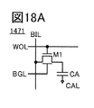
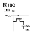
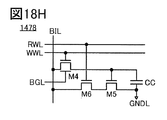
- 18A to 18H are circuit diagrams showing a configuration example of a storage device.
- FIG. 12 is a circuit diagram showing a configuration example of a circuit included in the arithmetic circuit.
- FIG. 13 is a timing chart showing an operation example of the arithmetic circuit.
- FIG. 14 is a block diagram showing a configuration example of the
- FIG. 19 is a schematic cross-sectional view showing a configuration example of the semiconductor device.
- FIG. 20 is a schematic cross-sectional view showing a configuration example of a semiconductor device.
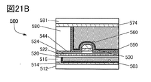
- 21A to 21C are schematic cross-sectional views showing a configuration example of a semiconductor device.
- 22A and 22B are schematic cross-sectional views showing a configuration example of a transistor.
- FIG. 23 is a schematic cross-sectional view showing a configuration example of the semiconductor device.
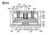
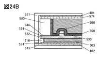
- 24A and 24B are schematic cross-sectional views showing a configuration example of a transistor.
- FIG. 25 is a schematic cross-sectional view showing a configuration example of the semiconductor device.
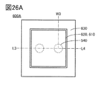
- FIG. 26A is a top view showing a configuration example of the capacitance.
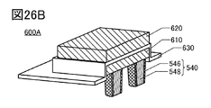
- FIG. 26B and 26C are cross-sectional perspective views showing a configuration example of the capacitance.
- FIG. 27A is a top view showing a configuration example of the capacitance.
- FIG. 27B is a cross-sectional view showing a configuration example of the capacitance.
- FIG. 27C is a cross-sectional perspective view showing a configuration example of the capacitance.
- FIG. 28A is a diagram showing the classification of the crystal structure of IGZO.
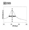
- FIG. 28B is a diagram showing an XRD spectrum of quartz glass.
- FIG. 28C is a diagram showing an XRD spectrum of crystalline IGZO.
- FIG. 28D is a diagram showing a microelectron diffraction pattern of crystalline IGZO.
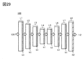
- FIG. 29 shows the configuration of the generator used in the embodiment.
- FIG. 30 is an image according to an embodiment.
- 31A and 31B are images according to an embodiment.
- FIG. 32 is an image according to an embodiment.
- DOSRAM registered trademark
- 1T transistor
- 1C capacity
- NOSRAM Nonvolatile Oxide Semiconductor RAM
- DOSRAM Nonvolatile Oxide Semiconductor RAM
- One aspect of the present invention is an inspection device having an electron microscope, a PC (Personal Computer), and a server, and an inspection method using the inspection device.
- the shape of a fine sample such as a semiconductor device can be inspected. Specifically, for example, it is possible to inspect whether or not the sample has an abnormal portion.
- a PC and a server are collectively referred to as a computer.
- the electron microscope has a function of photographing a sample.
- the image taken by the electron microscope is sent to the computer as an inspection image.
- the computer has an AI chip which is a circuit in which a neural network is constructed, and the neural network is trained in advance using, for example, only an image of a sample having no abnormal portion as teacher data.
- the inspection image sent to the computer is input to the circuit in which the neural network is configured.
- the circuit produces an image. Therefore, it can be said that the circuit has a function as a generator.
- the training of the neural network is performed using, for example, only the image of the sample having no abnormal portion as the teacher data. Therefore, even if the inspection image input to the circuit in which the neural network is configured is an image including an abnormal portion, the abnormal portion disappears from the output image.
- the computer included in the inspection device of one aspect of the present invention performs smoothing processing on the inspection image and the image output from the neural network. Then, by taking the difference between the smoothed inspection image and the image output from the neural network, an abnormal portion included in the inspection image is detected.
- the inspection device of one aspect of the present invention can automatically detect an abnormality included in an inspection image with high accuracy.
- FIG. 1 is a block diagram showing a configuration example of the inspection device 1 which is one embodiment of the present invention.
- the inspection device 1 includes an electron microscope 10, an image processing device 80, a PC 20, and a server 30.
- the PC 20 and the server 30 are collectively referred to as a computer 40.
- the inspection device 1 having the configuration shown in FIG. 1 is suitable for inspecting the shape of a fine sample such as a semiconductor device. In particular, it is suitable for inspecting the shape of a sample of several ⁇ m or less.
- the electron microscope 10 will be described assuming SEM, but the present invention is not limited to this, and one embodiment of the present invention is a transmission electron microscope (TEM: Transmission Electron Microscope) or a scanning transmission electron microscope (TEM). It is also applicable to STEM: Scanning Transmission Electron Microscope).
- TEM Transmission Electron Microscope
- TEM scanning transmission electron microscope
- the electron microscope 10 includes an electron gun 11, a focusing lens 12, an objective lens 13, a scanning coil 14, a detector 15, and a stage 16. Further, although not shown, the electron microscope 10 has a vacuum pump and can keep the sample chamber in a vacuum state.
- the electron beam 17 emitted from the electron gun 11 is focused by the focusing lens 12 and the objective lens 13 and irradiated to the sample 18.
- the sample 18 emits a signal electron 19, and the signal electron 19 is detected by the detector 15.
- the signal electrons 19 include secondary electrons and backscattered electrons.
- the secondary electrons and backscattered electrons may be detected by separate detectors.
- the inspection device 1 can observe the surface shape and the like of the sample 18 by analyzing the intensity of the signal electron 19.
- the electron microscope 10 has a function of generating a signal corresponding to the surface shape and the like of the sample 18.
- the image processing device 80 has a function of converting a signal into an image.
- the image processing device 80 converts the signal detected by the detector 15 into an image.
- the image generated by the image processing device 80 is sent to the PC 20.
- the PC 20 has an input / output device 21.
- the user of the inspection device 1 can confirm the image generated by the image processing device 80 through the input / output device 21.
- the image is represented by a pixel value.
- the pixel value is, for example, a value representing the brightness of the light emitted by the pixel.
- the image can be represented by the same number of pixel values as the resolution.
- an image having a resolution of 1920 ⁇ 1080 can be represented by a pixel value of 1920 ⁇ 1080.
- the input / output device 21 is a so-called interface, and includes a display, a keyboard, a mouse, and the like.
- a touch sensor may be provided on the display.
- the PC 20 has a function of controlling the electron microscope 10, and can control the accelerating voltage of the electron beam, the position of the stage, and the like.
- the PC 20 is connected to the server 30 via a network, and can send the image taken by the electron microscope 10 to the server 30.
- the server 30 has a CPU (Central Processing Unit) 31, an AI chip 32, a main storage device 33, an auxiliary storage device 34, and a bus 35.
- CPU Central Processing Unit
- the server 30 can analyze the image signal sent from the PC 20 and send the analysis result to the PC 20.
- DRAM can be used as the main storage device 33. Further, DOSRAM or NOSRAM may be used as the main storage device 33. By using DOSRAM or NOSRAM, the power consumption of the server 30 can be suppressed.
- auxiliary storage device 34 an HDD (Hard Disk Drive) or an SSD (Solid State Drive) can be used. Further, NO SRAM may be used as the auxiliary storage device 34. By using NO SRAM, the power consumption of the server 30 can be suppressed.
- HDD Hard Disk Drive
- SSD Solid State Drive
- the AI chip 32 is a circuit in which a neural network is configured. It is preferable to use an OS transistor for the AI chip 32. By using an OS transistor in the AI chip 32, an analog neural network becomes possible, and the power consumption of the server 30 can be suppressed.
- the PC 20 may have the role of the server 30. In that case, the PC 20 preferably has an AI chip 32.
- the image taken by the electron microscope 10 is analyzed by the server 30.
- the server 30 can automatically detect an abnormal portion included in the image and notify the user of the inspection device 1 via the PC 20 and the input / output device 21.
- the sample 18 is assumed to be a semiconductor device, but the sample 18 is not limited to this.
- the sample 18 the whole sample whose shape is generally confirmed by an electron microscope is applicable.
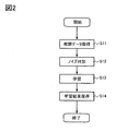
- FIG. 2 shows a flowchart showing an example of the flow of the learning process
- FIGS. 3A to 3C are schematic views for explaining a part of the process of FIG. In this embodiment, a case of inspecting the wiring shape of the semiconductor device will be illustrated and described.
- the processing shown in FIG. 2 is preferably performed on the server 30, but in some cases, some or all of the processing may be performed on the PC 20.
- the teacher data 101 is acquired. It is preferable that the teacher data 101 is composed of only a plurality of non-defective images that do not include abnormal parts.
- the number of non-defective images is preferably 1,000 or more, more preferably 5,000 or more, and even more preferably 10,000 or more. If the number of non-defective images is large, more accurate learning is possible, but in reality, it is limited by the performance of the server 30 that performs learning. Specifically, it is limited by the processing capacity of the CPU 31 and the AI chip 32 and the storage capacity of the main storage device 33.
- step S11 it is preferable to convert the resolution of the image constituting the teacher data 101 into an appropriate value.
- the higher the resolution of the image the more accurate learning is possible, but in reality, it is limited by the performance of the server 30 that performs learning. Specifically, it is limited by the processing capacity of the CPU 31 and the AI chip 32 and the storage capacity of the main storage device 33.
- step S11 it is preferable that the number of channels of the image constituting the teacher data 101 is converted to 1, that is, grayscale.
- step S12 noise is added to all the images of the teacher data 101 to generate the data 102 (FIG. 3A).
- Examples of the noise to be added include Gaussian noise and the like.
- step S13 learning is performed. Learning is performed using the teacher data 101, the data 102, and the generator 100 (FIG. 3B).
- the generator 100 is a program using a neural network, and can generate an image for the input data.
- Examples of the generator 100 include an Autoencoder (AE), a Convolutional Autoencoder (CAE), and the like.
- AE Autoencoder
- CAE Convolutional Autoencoder
- GAN Generative Adversarial Networks
- DCGAN Deep Convolutional Generative Adversarial Networks
- the AI chip 32 has a function as a generator 100.
- the generator 100 uses the data 102 as input data and performs learning so that the output data approaches the teacher data 101 (updates the weight of the neural network).
- step S14 the learning result 103 is saved (FIG. 3B). More specifically, the weight of the generator 100 acquired by learning is stored.
- the above-mentioned learning is performed for each wiring shape to be inspected. That is, the learning result corresponding to the type of the wiring shape to be inspected is acquired.
- FIG. 3C shows three types of wiring shapes, which are teacher data 101a, teacher data 101b, and teacher data 101c, respectively. Further, as a result of using each teacher data for learning, a learning result 103a, a learning result 103b, and a learning result 103c are acquired. These learning results are stored in the auxiliary storage device 34 of the server 30.
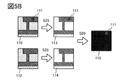
- FIG. 4 is a flowchart showing an example of the flow of the inspection process described above, and FIGS. 5A to 5C, 6A, 6B, and 7A and 7B are schematics for explaining a part of the process of FIG. It is a figure.
- the processing shown in FIG. 4 is preferably performed on the server 30, but in some cases, some or all of the processing may be performed on the PC 20.
- the process of FIG. 4 is preferably performed by the PC 20.
- the PC 20 preferably has an AI chip 32.
- step S21 the server 30 acquires an image taken by the electron microscope 10.
- step S22 the server 30 checks whether the trained model corresponding to the acquired image exists in the auxiliary storage device 34. If it exists, the process proceeds to step S23, and if it does not exist, the inspection is terminated. Before the inspection is completed, it is preferable to output a message to the effect that the learned data does not exist to the input / output device 21 and notify the user of the inspection device 1.
- step S21 it is preferable that the resolution and the number of channels of the inspection image 110 are matched with the teacher data 101 in step S13 of FIG.
- step S23 noise is added to the inspection image 110 to generate an image 120 (FIG. 5A). It is desirable that the noise to be added is the same as that added in step S12 of FIG.
- step S24 the image 120 is input to the trained generator 100, and the image 112 is acquired (FIG. 5A).
- the generator 100 is in a state of reading the learning result 103 acquired by the prior learning, and the weight is updated.
- the generator 100 Since the generator 100 has learned only with the teacher data 101, which is a set of non-defective images, no information about the abnormal portion 111 is given. Therefore, the generator 100 cannot reproduce the abnormal portion 111, and the abnormal portion 111 disappears from the image 112.
- step S25 the inspection image 110 is smoothed and the image 113 is acquired. Similarly, the image 112 is smoothed to obtain the image 114 (FIG. 5B). It is preferable that the smoothing process performed on the inspection image 110 and the image 112 is the same.
- a method of the smoothing process there is a method of calculating the convolution between the image and a filter called a kernel.
- a filter there are two types, an average filter and a Gaussian filter.
- the smoothing processing method a case where a 3 ⁇ 3 size average filter is used will be described.
- a 3 ⁇ 3 window centered on that pixel is selected for each pixel, and the total pixel values of all the pixels in the window is 9 Divide by. That is, it takes the average of the pixel values in the window.
- the size of the filter is not limited to Equation 1, and a size represented by an odd square such as 5 ⁇ 5 or 7 ⁇ 7 may be provided as needed.
- the weights of the average filters were all 1, but the Gaussian filter was given the weights of the filters according to the Gaussian distribution centered on the pixel of interest.
- the Gaussian filter When applying a Gaussian filter, specify the variance (or standard deviation) of the Gaussian distribution.
- the inspection image 110 often contains noise derived from the electron microscope 10. By performing the above-mentioned smoothing process, noise can be removed from the inspection image 110.
- step S26 the difference between the image 113 and the image 114 is taken.
- the image 115 is acquired by taking the difference between the pixel value representing the image 113 and the pixel value representing the image 114 (FIG. 5B).
- the difference is taken for each pixel value. That is, when the image 113 and the image 114 are represented by, for example, 1920 ⁇ 1080 pixel values, a difference is taken for each of the 1920 ⁇ 1080 pixel values. Therefore, when the image 113 and the image 114 are each represented by 1920 ⁇ 1080 pixel values, the image 115 can also be represented by 1920 ⁇ 1080 pixel values.
- the difference between the image 113 and the image 114 is close to zero. Therefore, in the image 115, the brightness is close to 0 except for the abnormal portion 111.
- step S27 the brightness of the pixels of the image 115 is converted into a binary value of 1 or 0 based on a certain threshold value. By doing so, it is possible to acquire an image 116 in which the abnormal portion 111 is painted white and the portion other than the abnormal portion 111 is painted black (FIG. 5C).
- the image 116 is an image in which the abnormal portion 111 is emphasized.
- step S28 outlier detection of the image 116 is performed, and the image 116 is classified into either abnormal data or normal data. That is, the machine determines the quality of the inspection image 110.
- an appropriate method such as a k-nearest neighbor method, a k-means method, a LOF (Local Outlier Factor), or an SVM (Support Vector Machine) method may be used.
- the degree of abnormality of the image 116 by a certain numerical value.
- the number of pixels whose brightness is represented by 1 the number of pixels filled in white
- the distance from the center of gravity of the set clustered as normal data may be used as the degree of anomaly.
- the distance from the boundary between normal and abnormal determined by the machine may be used as the degree of abnormality.
- weighting may be performed for abnormalities.
- the magnitude of the weight can be different for each type of anomaly, for example. For example, anomalies that have a large effect on the quality of the test sample can be given a large weight.
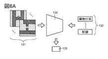
- weighting an abnormality for example, all the abnormality points 111 detected from the inspection image 110 can be weighted, and the total weight can be used as the degree of abnormality.
- FIG. 6A and 6B are schematic views for explaining an example of a weighting method for anomalies.
- FIG. 6A is a schematic diagram for explaining an example of the learning method, and is performed in advance.
- FIG. 6B is a schematic diagram for explaining an example of a method of determining the type of abnormality from an inspection image including an abnormality by using the learning result.
- FIGS. 6A and 6B are preferably performed on the server 30, but in some cases, some or all of the processes may be performed on the PC 20.
- the process of FIG. 6B is preferably performed by the PC 20.
- the PC 20 preferably has an AI chip 32.
- the image data 131 is acquired, and the label 132 is associated with each of the acquired image data 131.
- the image data 131 is preferably composed of only a plurality of defective image images including abnormal parts.
- the label 132 may represent, for example, the type of abnormality shown in the image data 131.
- the type of abnormality can be, for example, disconnection, short circuit, foreign matter adhesion, cavity formation, or the like.
- the number of defective image images is, for example, preferably 1,000 or more, more preferably 5,000 or more, and more preferably 10,000 or more for one type of abnormality. If the number of defective images is large, more accurate learning is possible, but in reality, it is limited by the performance of the server 30 that performs learning. Specifically, it is limited by the processing capacity of the CPU 31 and the AI chip 32 and the storage capacity of the main storage device 33.
- the resolution of the image constituting the image data 131 it is preferable to convert the resolution of the image constituting the image data 131 to an appropriate value.
- the higher the resolution of the image the more accurate learning is possible, but in reality, it is limited by the performance of the server 30 that performs learning. Specifically, it is limited by the processing capacity of the CPU 31 and the AI chip 32 and the storage capacity of the main storage device 33.
- the number of channels of the image constituting the image data 131 is 1, that is, converted to gray scale.
- the learning is performed using the image data 131, the label 132, and the classifier 130 (FIG. 6A).
- the classifier 130 is a program using a neural network, and can extract the feature amount of the input image and generate a feature map.
- Examples of the classifier 130 include a convolutional neural network (CNN: Convolutional Neural Network) and the like. It can be said that the AI chip 32 has a function as a classifier 130.
- the classifier 130 uses the image data 131 and the label 132 as teacher data, and performs learning so that the output data becomes desired (updates the weight of the neural network). For example, when the classifier 130 outputs a feature map, learning is performed so that the classifier 130 can appropriately extract the feature amount of the image data 131 input to the classifier 130 according to the label 132.
- the learning result 133 is saved (FIG. 6A). More specifically, the weight of the classifier 130 acquired by learning is stored. This is the end of learning.
- step S28 shown in FIG. 4 the inspection image in which the abnormality is detected is input to the trained classifier 130.
- FIG. 6B shows an example in which the inspection image 110 including the abnormal portion 111 is input to the classifier 130.
- the classifier 130 is in a state of reading the learning result 133 acquired by the prior learning, and the weight is updated.
- data 134 indicating the type of abnormality included in the inspection image is output from the classifier 130 based on the learning result 133.
- the degree of abnormality of the inspection image 110 including the abnormal portion 111 is calculated.
- the degree of anomaly can be a value obtained by multiplying the number of anomalies by the weight corresponding to the data 134.
- the inspection image 110 is smoothed to obtain an image 113, and the image 112 is smoothed to obtain an image 114, and then the image 113 is used. Take the difference of the image 114.
- the inspection image 110 often contains noise derived from the electron microscope 10. Therefore, if the difference is taken without performing the smoothing process, the abnormal portion 111 may not be detected correctly. Therefore, by taking the difference after performing the smoothing process, the inspection device 1 can automatically detect the abnormal portion 111 included in the inspection image 110 with high accuracy.
- FIG. 7A is a schematic diagram showing an example in which the above-mentioned inspection result is displayed on the input / output device 21.
- FIG. 7A shows a terminal provided with a touch panel and a display as an example of the input / output device 21.
- the inspection images are displayed side by side in the order of the degree of abnormality acquired in step S28.
- FIG. 7A shows an example in which the image on the left side has a smaller degree of abnormality and the image on the right side has a larger degree of abnormality (Abnormal). That is, good products are on the left side, and defective products are on the right side.
- the result (Good / Bad) of the quality determination by the machine in step S28 is displayed on each image.
- FIG. 7A shows an example in which the inspection image 110 touched by the user of the inspection device 1 and the image 117 are displayed.
- Image 117 is a composite of the inspection image 110 and the image 116 of FIG. 5C. That is, it is an image in which the abnormal portion of the inspection image 110 is emphasized.
- the user of the inspection device 1 can easily determine the abnormal portion included in the inspection image.
- the color of the abnormal portion may be displayed in gradation according to the brightness of the image 115 in FIG. 5B.
- the input / output device 21 allows the user to correct the Good / Bad result determined by the machine.
- the correction result can be transmitted to the server 30 and reflected in the future pass / fail judgment.
- the images existing near the left and right ends are unlikely to be judged differently between the machine and the user of the inspection device 1.
- the image existing near the center of the screen is often judged differently between the machine and the user of the inspection device 1.
- FIG. 7B is a schematic view showing a display example of the input / output device 21 when weighting an abnormal portion of the inspection image 110.
- the weight can be made larger as the influence on the quality of the test sample is greater, for example. Weighting can be performed by the method shown in FIGS. 6A and 6B.
- FIG. 7B shows an example in which the image 117 corresponding to the inspection image 110 touched by the user of the inspection device 1 is displayed.
- the image 117 shown in FIG. 7B includes two abnormal locations.
- one of the abnormal parts does not cause disconnection, short circuit, etc., and the influence of the abnormality on the quality of the inspection sample is small.
- the other abnormal portion causes, for example, a disconnection, and the abnormality has a great influence on the quality of the inspection sample. Therefore, the weight of the other abnormal portion is made larger than the weight of one abnormal portion.
- FIG. 7B shows a display example of the input / output device 21 when the weight of one abnormal portion is 2 and the weight of the other abnormal portion is 10. As shown in FIG. 7B, the weight can be displayed for each abnormal portion.
- FIG. 7B shows a display example of the input / output device 21 when the total weight is 5 or less, it is determined to be a good product (Good), and when it is 6 or more, it is determined to be a defective product (Bad).
- the determination criteria for good products (Good) and defective products (Bad) can be displayed on the input / output device 21.
- the abnormal part By weighting the abnormal part, it is possible to judge the quality of the test sample with high accuracy. Further, by displaying the weight on the input / output device 21, the user of the inspection device 1 can easily recognize the cause of the defect of the sample.
- the inspection device of the present embodiment it is possible to automatically detect an abnormality included in the inspection image with high accuracy. In addition, it can be automatically detected with low power consumption.
- the inspection method of the present embodiment it is possible to automatically detect an abnormality included in the inspection image with high accuracy. In addition, it can be automatically detected with low power consumption.
- an image taken by an electron microscope is assumed as an inspection image in which the inspection apparatus of one aspect of the present invention determines an abnormality, but one aspect of the present invention is not limited to this.
- a configuration example of the inspection device according to one aspect of the present invention will be described when an image other than the image taken by the electron microscope is used as the inspection image.
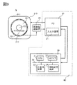
- FIG. 8 is a block diagram showing a configuration example of the inspection device 1a.
- the inspection device 1a differs from the inspection device 1 shown in the first embodiment in that it has a computed tomography apparatus 50 instead of the electron microscope 10.
- the computed tomography apparatus 50 has a gantry 51 and a cradle 52.
- the gantry 51 is provided with an opening 61, and an X-ray tube 71 and a detector 72 are provided so as to have a region in contact with the side wall of the opening 61.
- the subject 62 is placed in the cradle 52.
- the subject 62 can be, for example, the human body.
- the X-ray tube 71 has a function of emitting, for example, X-rays (for example, an electromagnetic wave having a wavelength of 1 pm or more and 10 nm or less).
- the detector 72 has a function of detecting, for example, X-rays.
- the electromagnetic wave emitted from the X-ray tube 71 is irradiated to the subject 62, a part of the irradiated electromagnetic wave is absorbed by the subject 62.
- the electromagnetic wave transmitted without being absorbed by the subject 62 is irradiated to the detector 72.
- the signal representing the intensity of the electromagnetic wave applied to the detector 72 is converted into an image by the image processing device 80.
- the inspection device 1 shown in the first embodiment can be referred to.
- the PC 20 included in the inspection device 1a has a function of controlling the computed tomography device 50, and can control the position of the X-ray tube 71, for example.
- the electron microscope 10 is read as the computed tomography device 50, the sample is read as the subject, and the like, the description of the inspection method using the inspection device 1 shown in the first embodiment will be described. You can refer to it.
- FIG. 9 is a block diagram showing a configuration example of the inspection device 1b.
- the inspection device 1b is different from the inspection device 1 shown in the first embodiment in that it has a nuclear magnetic resonance device 210 instead of the electron microscope 10.
- the nuclear magnetic resonance apparatus 210 has a gantry 211 and a cradle 212.
- the gantry 211 is provided with an opening 221.
- a coil 231 is provided inside the gantry 211 so as to cover the side wall of the opening 221.
- Subject 222 is placed in the cradle 212.
- the subject 222 can be, for example, a human body in the same manner as the subject 62 shown in FIG.
- the subject 222 is preferably a living body.
- the coil 231 has a function of generating a magnetic field.
- a resonance phenomenon occurs between the hydrogen atom contained in the subject 222 and the magnetic field.
- a nuclear magnetic resonance signal is generated.
- the nuclear magnetic resonance signal is converted into an image by the image processing device 80.
- the inspection device 1 shown in the first embodiment can be referred to.
- the PC 20 included in the inspection device 1b has a function of controlling the nuclear magnetic resonance device 210, and can switch the direction of the magnetic field generated by the coil 231, for example.
- the electron microscope 10 is read as a nuclear magnetic resonance device 210, the sample is read as a subject, and the like, the description of the inspection method using the inspection device 1 shown in the first embodiment will be described. Can be referred to.
- a hierarchical neural network has one input layer, one or more intermediate layers (hidden layers), and one output layer, and is composed of a total of three or more layers.
- the hierarchical neural network 200 shown in FIG. 10A shows an example thereof, and the neural network 200 has a first layer to an R layer (R here can be an integer of 4 or more). ing.
- R can be an integer of 4 or more
- the first layer corresponds to the input layer
- the R layer corresponds to the output layer
- the other layers correspond to the intermediate layer.
- FIG. 10A shows the (k-1) th layer and the kth layer (k here is an integer of 3 or more and R-1 or less) as intermediate layers, and other intermediate layers. Is not shown.
- Each layer of the neural network 200 has one or more neurons.
- layer 1 has neurons N 1 (1) to neuron N p (1) (where p is an integer greater than or equal to 1), and layer (k-1) is neuron N 1. (K-1) to neuron N m (k-1) (where m is an integer of 1 or more), and the k-th layer has neurons N 1 (k) to neurons N n (k) ( Here, n is an integer of 1 or more), and the R layer has neurons N 1 (R) to neurons N q (R) (q here is an integer of 1 or more). ..
- the values of m and n may be greater than or equal to p and less than or equal to p. Further, the values of m and n may be q or more and less than q. For example, when the neural network 200 has a function as an autoencoder (AE), the values of m and n can be less than p and q.
- AE autoencoder
- 10B is a neuron N j of the k-th layer (k), shows the signal which is input to the neuron N j (k), a signal output from the neuron N j (k), the.
- z 1 (k-1) to z m (k- ), which are output signals of neurons N 1 (k-1) to N m (k-1) in the (k-1) layer , respectively. 1) is output toward the neuron Nj (k) .
- the neuron N j (k) is, z 1 (k-1) to z m (k-1) to generate a z j (k) in response to, the z j (k) is an output signal (k + 1 ) Output to each neuron in the layer (not shown).
- the degree of signal transmission of signals input from neurons in the previous layer to neurons in the next layer is determined by the strength of synaptic connections (hereinafter referred to as weighting factors) that connect these neurons.
- weighting factors the strength of synaptic connections that connect these neurons.
- the signal output from the neurons in the previous layer is multiplied by the corresponding weighting factor and input to the neurons in the next layer.
- i an integer 1 or m
- the signal input to the neuron N j (k) in the k-th layer can be expressed by the equation (D1).
- the result of the sum of products may be biased as a bias.
- the equation (D2) can be rewritten as the following equation.
- the neuron N j (k) produces an output signal z j (k) in response to u j (k) .
- Neuron N j output signal z j from (k) (k) defined by the following equation.
- the function f (u j (k) ) is an activation function in a hierarchical neural network, and a step function, a linear ramp function, a sigmoid function, or the like can be used.
- the activation function may be the same or different in all neurons.
- the activation function of neurons may be the same or different in each layer.
- the signal, the weighting coefficient w, or the bias b output by the neurons in each layer may be an analog value or a digital value.
- the digital value may be, for example, a binary value or a ternary value. A value with a larger number of bits may be used.
- an analog value for example, a linear ramp function, a sigmoid function, or the like may be used as the activation function.
- binary digital values for example, a step function with an output of -1 or 1 or 0 or 1 may be used.
- the signal output by the neurons in each layer may have three or more values.
- the activation function has three or more values, for example, a step function whose output is -1, 0, or 1, or 0, 1, or.
- a step function or the like set to 2 may be used.
- a step function of -2, -1, 0, 1, or 2 may be used.
- the neural network 200 is sequentially input from the front layer in each layer from the first layer (input layer) to the last layer (output layer). Based on the signal, an output signal is generated using the equation (D1), the equation (D2) (or the equation (D3)), and the equation (D4), and the output signal is output to the next layer.
- the signal output from the last layer (output layer) corresponds to the result calculated by the neural network 200.
- FIG. 11 shows a configuration example of the arithmetic circuit MAC1.
- the arithmetic circuit MAC1 shown in FIG. 11 performs a product-sum operation of the first data held in the memory cell described later and the input second data, and activates the activation function using the result of the product-sum operation. It is a circuit that performs the calculation of.
- the first data and the second data can be analog data or multi-valued data (discrete data) as an example.
- the arithmetic circuit MAC1 includes a current source circuit CS, a current mirror circuit CM, a circuit WDD, a circuit WLD, a circuit CLD, a circuit OFST, an activation function circuit ACTV, and a memory cell array CA.
- the memory cell array CA has a memory cell AM [1], a memory cell AM [2], a memory cell AMref [1], and a memory cell AMref [2].
- the memory cell AM [1] and the memory cell AM [2] have a role of holding the first data, and the memory cell AMref [1] and the memory cell AMref [2] are used to perform the product-sum operation. It has a function to hold the required reference data.
- the reference data can be analog data or multi-valued data (discrete data) as well as the first data and the second data.
- the memory cell array CA of FIG. 11 two memory cells are arranged in the row direction and two in the column direction in a matrix, whereas in the memory cell array CA, three or more memory cells are arranged in the row direction and columns. Three or more in the direction may be arranged in a matrix. Further, when multiplication is performed instead of the multiply-accumulate operation, the memory cell array CA may be configured such that one memory cell in the row direction and two or more memory cells in the column direction are arranged in a matrix.
- the memory cell AM [1], the memory cell AM [2], the memory cell AMref [1], and the memory cell AMref [2] have a transistor Tr11, a transistor Tr12, and a capacitance C1, respectively.
- the transistor Tr11 is preferably an OS transistor.
- the channel formation region of the transistor Tr11 is indium, element M (element M is, for example, aluminum, gallium, yttrium, copper, vanadium, beryllium, boron, titanium, iron, nickel, germanium, zirconium, molybdenum, lantern. , One or more selected from cerium, neodymium, hafnium, tantalum, tungsten, gallium and the like.), It is more preferable that the oxide contains at least one of zinc. It is more preferable that the transistor Tr11 has a transistor structure described in the following embodiments.
- the leakage current of the transistor Tr11 can be suppressed, so that a product-sum calculation circuit with high calculation accuracy may be realized. Further, by using the OS transistor as the transistor Tr11, the leakage current from the holding node to the writing word line when the transistor Tr11 is in the non-conducting state can be made very small. That is, since the potential refresh operation of the holding node can be reduced, the power consumption of the product-sum calculation circuit can be reduced.
- the transistor Tr12 can be manufactured at the same time as the transistor Tr11, so that the manufacturing process of the product-sum calculation circuit may be shortened.
- the channel forming region of the transistor Tr12 may contain silicon instead of oxide.
- the silicon for example, amorphous silicon, microcrystalline silicon, polycrystalline silicon, single crystal silicon, hydride amorphous silicon and the like may be used.
- the first terminal of the transistor Tr11 is the gate of the transistor Tr12 and electricity. Is connected.
- the first terminal of the transistor Tr12 is electrically connected to the wiring VR.
- the first terminal of the capacitance C1 is electrically connected to the gate of the transistor Tr12.
- the second terminal of the transistor Tr11 is electrically connected to the wiring WD, and the gate of the transistor Tr11 is electrically connected to the wiring WL [1].
- the second terminal of the transistor Tr12 is electrically connected to the wiring BL, and the second terminal of the capacitance C1 is electrically connected to the wiring CL [1].
- the connection point between the first terminal of the transistor Tr11, the gate of the transistor Tr12, and the first terminal of the capacitance C1 is a node NM [1].
- the current flowing from the wiring BL to the second terminal of the transistor Tr12 is defined as I AM [1] .
- the second terminal of the transistor Tr11 is electrically connected to the wiring WD, and the gate of the transistor Tr11 is electrically connected to the wiring WL [2].
- the second terminal of the transistor Tr12 is electrically connected to the wiring BL, and the second terminal of the capacitance C1 is electrically connected to the wiring CL [2].
- the connection point between the first terminal of the transistor Tr11, the gate of the transistor Tr12, and the first terminal of the capacitance C1 is a node NM [2].
- the current flowing from the wiring BL to the second terminal of the transistor Tr12 is defined as I AM [2] .
- the second terminal of the transistor Tr11 is electrically connected to the wiring WDref, and the gate of the transistor Tr11 is electrically connected to the wiring WL [1].
- the second terminal of the transistor Tr12 is electrically connected to the wiring BLref, and the second terminal of the capacitance C1 is electrically connected to the wiring CL [1].
- the connection point between the first terminal of the transistor Tr11, the gate of the transistor Tr12, and the first terminal of the capacitance C1 is a node NMref [1].
- the current flowing from the wiring BLref to the second terminal of the transistor Tr12 is defined as IAMref [1] .
- the second terminal of the transistor Tr11 is electrically connected to the wiring WDref, and the gate of the transistor Tr11 is electrically connected to the wiring WL [2].
- the second terminal of the transistor Tr12 is electrically connected to the wiring BLref, and the second terminal of the capacitance C1 is electrically connected to the wiring CL [2].
- the connection point between the first terminal of the transistor Tr11, the gate of the transistor Tr12, and the first terminal of the capacitance C1 is a node NMref [2].
- the current flowing from the wiring BLref to the second terminal of the transistor Tr12 is defined as IAMref [2] .
- node NM [1], node NM [2], node NMref [1], and node NMref [2] function as holding nodes of their respective memory cells.
- the wiring VR allows a current to flow between the first terminal and the second terminal of each transistor Tr12 of the memory cell AM [1], the memory cell AM [2], the memory cell AMref [1], and the memory cell AMref [2].
- Wiring for. Therefore, the wiring VR functions as a wiring for giving a predetermined potential.
- the potential given by the wiring VR can be a reference potential or a potential lower than the reference potential.
- the current source circuit CS is electrically connected to the wiring BL and the wiring BLref.
- the current source circuit CS has a function of supplying a current to the wiring BL and the wiring BLref.
- the amount of current supplied to each of the wiring BL and the wiring BLref may be different from each other. In this configuration example, the current flowing from the current source circuit CS wiring BL and I C, the current flowing from the current source circuit CS wiring BLref and I Cref.
- the current mirror circuit CM has a wiring IL and a wiring ILref.
- the wiring IL is electrically connected to the wiring BL, and in FIG. 11, the connection point between the wiring IL and the wiring BL is shown as a node NP.
- the wiring ILref is electrically connected to the wiring BLref, and in FIG. 11, the connection point between the wiring ILref and the wiring BLref is a node NPref.
- the current mirror circuit CM has a function of discharging a current corresponding to the potential of the node NPref from the node NPref of the wiring BLref to the wiring ILref, and discharging the same amount of current from the node NP of the wiring BL to the wiring IL.
- the circuit WDD is electrically connected to the wiring WD and the wiring WDref.
- the circuit WDD has a function of transmitting data to be stored in each memory cell of the memory cell array CA.
- the circuit WLD is electrically connected to the wiring WL [1] and the wiring WL [2].
- the circuit WLD has a function of selecting a memory cell to write data to when writing data to a memory cell included in the memory cell array CA.
- the circuit CLD is electrically connected to the wiring CL [1] and the wiring CL [2].
- the circuit CLD has a function of applying a potential to the second terminal of the capacity C1 of each memory cell of the memory cell array CA.
- the circuit OFST is electrically connected to the wiring BL and the wiring OL.
- the circuit OFST has a function of measuring the amount of current flowing from the wiring BL to the circuit OFST and / or the amount of change in the current flowing from the wiring BL to the circuit OFST.
- the circuit OFST has a function of outputting the measurement result to the wiring OL.
- the circuit OFST may be configured to output the measurement result as a current to the wiring OL as it is, or may be configured to convert the measurement result into a voltage and output it to the wiring OL.
- the current flowing from the wiring BL to the circuit OFST is indicated by I ⁇ .
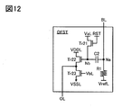
- the circuit OFST can have the configuration shown in FIG. In FIG. 12, the circuit OFST includes a transistor Tr21, a transistor Tr22, a transistor Tr23, a capacitance C2, and a resistance element R1.
- the first terminal of the capacitance C2 is electrically connected to the wiring BL, and the first terminal of the resistance element R1 is electrically connected to the wiring BL.
- the second terminal of the capacitance C2 is electrically connected to the first terminal of the transistor Tr21, and the first terminal of the transistor Tr21 is electrically connected to the gate of the transistor Tr22.
- the first terminal of the transistor Tr22 is electrically connected to the first terminal of the transistor Tr23, and the first terminal of the transistor Tr23 is electrically connected to the wiring OL.
- the electrical connection point between the first terminal of the capacitance C2 and the first terminal of the resistance element R1 is a node Na, the second terminal of the capacitance C2, the first terminal of the transistor Tr21, and the gate of the transistor Tr22. Let the electrical connection point of, be node Nb.
- the second terminal of the resistance element R1 is electrically connected to the wiring VrefL.
- the second terminal of the transistor Tr21 is electrically connected to the wiring VaL, and the gate of the transistor Tr21 is electrically connected to the wiring RST.
- the second terminal of the transistor Tr22 is electrically connected to the wiring VDDL.
- the second terminal of the transistor Tr23 is electrically connected to the wiring VSSL, and the gate of the transistor Tr23 is electrically connected to the wiring VbL.
- the wiring VrefL is a wiring that gives the potential Vref
- the wiring VaL is a wiring that gives the potential Va
- the wiring VbL is a wiring that gives the potential Vb.
- the wiring VDDL is the wiring that gives the potential VDD
- the wiring VSSL is the wiring that gives the potential VSS.
- the potential VDD is set to a high level potential
- the potential VSS is set to a low level potential.
- the wiring RST is a wiring that gives a potential for switching between a conductive state and a non-conducting state of the transistor Tr21.
- the source follower circuit is composed of the transistor Tr22, the transistor Tr23, the wiring VDDL, the wiring VSSL, and the wiring VbL.
- the resistance element R1 and the wiring VrefL give the node Na a current flowing from the wiring BL and a potential corresponding to the resistance of the resistance element R1.
- the first current (hereinafter referred to as the first current) flows from the wiring BL, the potential corresponding to the first current and the resistance of the resistance element R1 to the node Na by the resistance element R1 and the wiring VrefL. Is given.
- the transistor Tr21 is brought into a conductive state, and the potential Va is given to the node Nb. After that, the transistor Tr21 is put into a non-conducting state.
- the second current (hereinafter referred to as the second current) flows from the wiring BL
- the resistance element R1 and the wiring VrefL make the node Na the same as when the first current flows.
- a potential corresponding to the second current and the resistance of the resistance element R1 is given.
- the potential of the node Nb since the node Nb is in a floating state, the potential of the node Nb also changes due to the capacitive coupling due to the change in the potential of the node Na.
- the change in the potential of the node Na is ⁇ V Na and the capacitive coupling coefficient is 1, the potential of the node Nb is Va + ⁇ V Na .
- the potential Va + ⁇ V Na ⁇ V th is output from the wiring OL.
- the potential ⁇ V Na can be output from the wiring OL.
- the potential ⁇ V Na is determined according to the amount of change from the first current to the second current, the resistance value of the resistance element R1, and the potential Vref. Since the resistance value of the resistance element R1 and the potential Vref can be known, the amount of change in the current flowing through the wiring BL can be obtained from the potential ⁇ V Na by using the circuit OFST shown in FIG. ..
- the activation function circuit ACTV is electrically connected to the wiring OL and the wiring NIL.
- the result of the amount of change in the current measured by the circuit OFST is input to the activation function circuit ACTV via the wiring OL.
- the activation function circuit ACTV is a circuit that performs an operation according to a predefined function system on the result.
- a function system for example, a sigmoid function, a tanh function, a softmax function, a ReLU function, a threshold function and the like can be used, and these functions are applied as activation functions in a neural network.
- FIG. 13 shows a timing chart of an operation example of the arithmetic circuit MAC1.
- the timing chart of FIG. 13 shows the wiring WL [1], the wiring WL [2], the wiring WD, the wiring WDref, the node NM [1], the node NM [2], the node NMref [1], at the time T01 to the time T09.
- the current I B -I alpha from the wiring BL, the memory cell AM of the memory cell array CA [1], indicate the sum of the current flowing through the memory cell AM [2].
- ⁇ From time T01 to time T02 a high level potential (denoted as High in FIG. 13) is applied to the wiring WL [1], and a low level potential (Low in FIG. 13) is applied to the wiring WL [2]. Indicated.) Is applied. In addition, a potential V PR ⁇ V W [1] larger than the ground potential (denoted as GND in FIG. 13) is applied to the wiring WD, and a potential V PR larger than the ground potential is applied to the wiring WDref. It has been applied. Further, a reference potential (denoted as REFP in FIG. 13) is applied to the wiring CL [1] and the wiring CL [2], respectively.
- REFP reference potential
- the potential V W [1] is a potential corresponding to one of the first data. Further, the potential V PR is a potential corresponding to the reference data.
- V th is the threshold voltage of the transistor Tr12.
- I AMref [1], 0 I AMref [1] 0 is as follows. It can be expressed by an expression.
- the time starts from time T02. Until T03, the respective potentials of the node NM [1], the node NM [2], the node NMref [1], and the node NMref [2] are maintained.
- the OS is applied to each transistor Tr11 of the memory cell AM [1], the memory cell AM [2], the memory cell AMref [1], and the memory cell AMref [2].
- the transistor By applying the transistor, the leakage current flowing between the first terminal and the second terminal of the transistor Tr11 can be reduced, so that the node NM [1], the node NM [2], the node NMref [1], and the node Each potential of NMref [2] can be held for a long time.
- a ground potential is applied to the wiring WD and the wiring WDref. Since the transistors Tr11 of the memory cell AM [1], the memory cell AM [2], the memory cell AMref [1], and the memory cell AMref [2] are in the off state, the wiring WD and the wiring WDref are used. By applying the potential of, the potentials held in each of the node NM [1], the node NM [2], the node NMref [1], and the node NMref [2] are not rewritten.
- the potential V W [2] is a potential corresponding to one of the first data.
- I AMref [2], 0 When the current flowing from the wiring BLref to the first terminal via the second terminal of the transistor Tr12 of the memory cell AMref [2] is set to I AMref [2], 0 , similarly, I AMref [2], 0 is as follows. It can be expressed by an expression.
- the current from the current source circuit CS is supplied to the wiring BLref.
- a current is discharged to the wiring BLref by the current mirror circuit CM, the memory cell AMref [1], and the memory cell AMref [2].
- the following equation holds according to Kirchhoff's law.
- the current from the current source circuit CS is supplied to the wiring BL.
- a current is discharged to the wiring BL by the current mirror circuit CM, the memory cell AM [1], and the memory cell AM [2].
- a current flows from the wiring BL to the circuit OFST.
- the current supplied from the current source circuit CS and I C the current flowing from the wiring BL to the circuit OFST I alpha, when a 0, the following expression holds with Kirchhoff's law.
- the potential V X [1] is a potential corresponding to one of the second data.
- the increase in the potential of the gate of the transistor Tr12 is the potential obtained by multiplying the potential change of the wiring CL [1] by the capacitive coupling coefficient determined by the configuration of the memory cell.
- the capacitive coupling coefficient is calculated from the capacitance of the capacitance C1, the gate capacitance of the transistor Tr12, the parasitic capacitance, and the like.
- the increase in the potential of the wiring CL [1] and the increase in the potential of the gate of the transistor Tr12 are described as the same value. This corresponds to setting each capacitance coupling coefficient in the memory cell AM [1] and the memory cell AMref [1] to 1.
- the capacitance coupling coefficient is 1, the potential V X [1] is applied to the second terminal of each capacitance C1 of the memory cell AM [1] and the memory cell AMref [1], so that the node NM [ 1] The potentials of 1] and the node NMref [1] increase by V X [1] , respectively.
- I AMref [1], 1 is as follows. It can be expressed by an expression.
- the wiring BLref like the period from time T04 to time T05, the current I Cref from the current source circuit CS are supplied. At the same time, a current is discharged to the wiring BLref by the current mirror circuit CM, the memory cell AMref [1], and the memory cell AMref [2].
- the current discharged by the current mirror circuit CM is ICM , 1 , the following equation holds according to Kirchhoff's law.
- the wiring BL similar to the period from time T04 to time T05, the current I C from the current source circuit CS are supplied. At the same time, a current is discharged to the wiring BL by the current mirror circuit CM, the memory cell AM [1], and the memory cell AM [2]. Further, a current flows from the wiring BL to the circuit OFST. In the wiring BL, when the current flowing from the wiring BL to the circuit OFST is I ⁇ , 1 , the following equation holds according to Kirchhoff's law.
- ⁇ I ⁇ Difference between the current I ⁇ , 0 flowing from the wiring BL to the circuit OFST between the time T04 and the time T05 and the current I ⁇ , 1 flowing from the wiring BL to the circuit OFST between the time T05 and the time T06.
- ⁇ I ⁇ will be referred to as a differential current in the arithmetic circuit MAC1.
- the differential current ⁇ I ⁇ can be expressed by the following equations using the equations (E1) to (E10).
- a reference potential is applied to the wiring CL [1] between the time T06 and the time T07.
- the reference potential is applied to the second terminal of the respective capacities C1 of the memory cell AM [1] and the memory cell AMref [1]
- the potentials of the node NM [1] and the node NMref [1] are applied. Returns to the potentials between time T04 and time T05, respectively.
- a potential V X [1] higher than the reference potential is applied to the wiring CL [1]
- a potential V X [2] higher than the reference potential is applied to the wiring CL [2].
- the potential V X [1] is applied to the second terminal of the respective capacities C1 of the memory cell AM [1] and the memory cell AMref [1], and the memory cell AM [2] and the memory cell AMref [2 ] are applied.
- the potential V X [2] is applied to the second terminal of each capacitance C1. Therefore, the potential of the gate of each transistor Tr12 of the memory cell AM [1], the memory cell AM [2], the memory cell AMref [1], and the memory cell AMref [2] rises.
- the capacitance coupling coefficient is 1, the potential V X [2] is applied to the second terminal of each capacitance C1 of the memory cell AM [2] and the memory cell AMref [2], so that the node NM [ 2] The potentials of 2] and the node NMref [2] rise by V X [2] , respectively.
- I AMref [2], 1 is as follows. It can be expressed by an expression.
- the wiring BLref like the period from time T04 to time T05, the current I Cref from the current source circuit CS are supplied. At the same time, a current is discharged to the wiring BLref by the current mirror circuit CM, the memory cell AMref [1], and the memory cell AMref [2].
- the current discharged by the current mirror circuit CM is ICM , 2 , the following equation holds according to Kirchhoff's law.
- the wiring BL similar to the period from time T04 to time T05, the current I C from the current source circuit CS are supplied. At the same time, a current is discharged to the wiring BL by the current mirror circuit CM, the memory cell AM [1], and the memory cell AM [2]. Further, a current flows from the wiring BL to the circuit OFST. In the wiring BL, when the current flowing from the wiring BL to the circuit OFST is I ⁇ , 3 , the following equation holds according to Kirchhoff's law.
- the differential current ⁇ I ⁇ to be obtained can be expressed by the following equations using the equations (E1) to (E8) and the equations (E12) to (E15).
- the difference current ⁇ I ⁇ input to the circuit OFST is a potential V W which is a plurality of first data and a potential V X which is a plurality of second data.
- the value corresponds to the sum of the products. That is, the value of the sum of products of the first data and the second data can be obtained by measuring the differential current ⁇ I ⁇ in the circuit OFST.
- a reference potential is applied to the wiring CL [1] and the wiring CL [2] between the time T08 and the time T09.
- the reference potential is applied to the second terminal of each capacitance C1 of the memory cell AM [1], the memory cell AM [2], the memory cell AMref [1], and the memory cell AMref [2].
- the potentials of the node NM [1], the node NM [2], the node NMref [1], and the node NMref [2] return to the potentials between the time T06 and the time T07, respectively.
- the potential applied to the wiring CL [1] and the wiring CL [2] may be lower than the reference potential REFP.
- REFP a potential lower than the reference potential REFP is applied to the wiring CL [1] and / or the wiring CL [2]
- the memory cell connected to the wiring CL [1] and / or the wiring CL [2] The potential of the holding node can be lowered by capacitive coupling.
- the product of the first data and one of the second data having a negative value can be performed.
- the wiring CL [2] the case of applying -V X [2] rather than V X [2]
- the differential current [Delta] I alpha expressed as the following formula be able to.
- a memory cell array CA having memory cells arranged in a matrix of 2 rows and 2 columns was dealt with, but a memory cell array with 1 row and 2 columns or more, or 3 rows or more and 3 columns.
- the product-sum operation can be performed on the above memory cell array.
- the product-sum calculation circuit uses one of the plurality of columns as a memory cell for holding the reference data (potential V PR ), so that the product-sum calculation process can be performed simultaneously for the number of the remaining columns among the plurality of columns. Can be executed. That is, by increasing the number of columns in the memory cell array, it is possible to provide a semiconductor device that realizes high-speed product-sum calculation processing. Further, by increasing the number of rows, the number of terms to be added in the product-sum operation can be increased.
- the difference current ⁇ I ⁇ when the number of rows is increased can be expressed by the following equation.
- each memory cell in the same column uses the weighting coefficient w s [k] s [k-1] (k) as the first data.
- the output signal z s [k] (k) of the kth layer s [k] neuron using the value of the activation function as a signal. Can be.
- each of the same columns has the weighting coefficient w s [L] s [L-1] (L) as the first data.
- the output signal z s [L] (L) of the s [L] neuron in the L layer is used as the signal of the activation function. Can be.
- the input layer described in the present embodiment may function as a buffer circuit that outputs an input signal to the second layer.
- the number of rows in the memory cell AM is the number of neurons in the front layer.
- the number of rows in the memory cell AM corresponds to the number of output signals of the neurons in the previous layer that are input to one neuron in the next layer.
- the number of columns in the memory cell AM becomes the number of neurons in the next layer.
- the number of columns in the memory cell AM corresponds to the number of output signals output from the neurons in the next layer. That is, since the number of rows and columns of the memory cell array of the arithmetic circuit is determined by the number of neurons in each of the previous layer and the next layer, the number of rows and columns of the memory cell array is determined according to the neural network to be constructed. And design it.
- the configuration of the arithmetic circuit described in the present embodiment may be changed depending on the situation.
- the arithmetic circuit MAC1 shown in FIG. 11 may be changed to the arithmetic circuit MAC1 shown in FIG.
- the arithmetic circuit MAC1 of FIG. 14 has a configuration in which the memory cell AMB is added to the column including the memory cell AM [1] and the memory cell AM [1] of the memory cell array CA with respect to the arithmetic circuit MAC1 of FIG. There is.
- the memory cell AMB is electrically connected to the wiring WD, the wiring BL, the wiring WLB, and the wiring CLB. Further, the wiring WLB is electrically connected to the circuit WLD, and the wiring CLB is electrically connected to the circuit CLD.
- connection point between the first terminal of the transistor Tr11, the gate of the transistor Tr12, and the first terminal of the capacitance C1 is a node NMB.
- the wiring WLB functions as a wiring that supplies a selection signal from the circuit WLD to the memory cell AMB when writing data to the memory cell AMB.
- the wiring CLB functions as wiring for applying a constant potential to the second terminal of the capacitance C1 of the memory cell AMB.
- the constant potential is preferably a ground potential or a low level potential.
- the ground potential is applied to the node NMB so that the transistor Tr12 of the memory cell AMB is turned off between the time T01 and the time T05.
- Low level potential or the potential provided by the wiring VR.
- the potential V BIAS is held in the node NMB from the time T05 to the time T09 so that an arbitrary current IBIAS flows between the source and drain of the transistor Tr12 of the memory cell AMB. ..
- IBIAS is expressed by the following equation.
- Equations (E20) and (E21) correspond to operations that further give an arbitrary bias to the result of the product-sum operation. That is, the calculation of the equation (D3) can be performed by using the calculation circuit MAC1 of FIG. Since the IBIAS is determined not by the potential of the node NMB but also by the potential given by the wiring CLB, for example, in the timing chart of FIG. 13, the transistor Tr12 of the memory cell AMB is turned off between the time T01 and the time T05. A ground potential is applied to the wiring CLB so as to be in a state, and the potential of the wiring CLB is changed from the ground potential to an arbitrary potential between the time T05 and the time T09, and the source-drain of the transistor Tr12 of the memory cell AMB is changed. An arbitrary current I BIAS may flow between them.
- FIG. 15 shows a configuration example of the arithmetic circuit MAC2.
- the arithmetic circuit MAC2 shown in FIG. 15 performs a product-sum calculation of the first data corresponding to the voltage held in each cell and the input second data, and is activated by using the result of the product-sum calculation. It is a circuit that performs function operations.
- the first data and the second data can be analog data or multi-valued data (discrete data) as an example.
- the arithmetic circuit MAC2 includes a circuit WCS, a circuit XCS, a circuit WSD, a circuit SWS1, a circuit SWS2, a cell array CA2, and a conversion circuit ITRZ [1] to a conversion circuit ITRZ [m].
- the cell array CA2 includes cell IM [1,1] to cell IM [m, n] (where m is an integer of 1 or more and n is an integer of 1 or more) and cell IMref [1].
- the cell IM [1,1] to the cell IM [m, n] have a function of holding a potential corresponding to the amount of current according to the first data, and the cell IMref [1] to the cell IMref [m] It has a function of supplying the signal lines XCL [1] to XCL [m] with a voltage corresponding to the second data required for performing the product-sum calculation with the held potential.
- n + 1 cells are arranged in the row direction
- m cells are arranged in the column direction
- the cell array CA2 has two or more cells in the row direction and one cell in the column direction.
- the configuration may be arranged in a matrix.
- the cell IM [1,1] to the cell IM [m, n] have a transistor F1, a transistor F2, and a capacitance C5, and the cell IMref [1] to the cell IMref [m] have a transistor F1m, respectively. It has a transistor F2m and a capacitance C5m.
- the transistor F1 and the transistor F1m include the case where they finally operate in the linear region when they are in the ON state. That is, it is assumed that the gate voltage, the source voltage, and the drain voltage of each of the above-mentioned transistors are appropriately biased to the voltage in the range of operation in the linear region.
- the transistor F1 and the transistor F1m may operate in the saturation region when they are in the ON state, and may operate in the linear region and may operate in the saturation region in a mixed manner.
- the transistor F2 and the transistor F2m include the case where the transistor operates in the subthreshold region (that is, the case where the gate-source voltage is lower than the threshold voltage in the transistor F2 or the transistor F2m). It shall be muted. That is, it is assumed that the gate voltage, the source voltage, and the drain voltage of each of the above-mentioned transistors are appropriately biased to the voltage in the range of operation in the subthreshold region. Therefore, the transistor F2 and the transistor F2m include the case where the transistor F2 operates so that an off-current flows between the source and the drain.
- the transistor F1 and / or the transistor F1m is preferably an OS transistor like the transistor Tr11.
- the channel formation region of the transistor F1 and / or the transistor F1m is indium, element M (element M is, for example, aluminum, gallium, yttrium, copper, vanadium, beryllium, boron, titanium, iron, nickel, germanium. , Zirconium, molybdenum, lanthanum, cerium, neodymium, hafnium, tantalum, tungsten, magnesium and the like, and one or more thereof.), It is more preferable that the oxide contains at least one of zinc. .. It is more preferable that the transistor Tr11 has a transistor structure described in the following embodiments.
- the leakage current of the transistor F1 and / or the transistor F1m can be suppressed, so that a product-sum calculation circuit with high calculation accuracy may be realized.
- the leakage current from the holding node to the write word line in the non-conducting state of the transistor F1 and / or the transistor F1m can be made very small. it can. That is, since the potential refresh operation of the holding node can be reduced, the power consumption of the product-sum calculation circuit can be reduced.
- the transistor F2 and / or the transistor F2m can also be operated in a wide current range in the subthreshold region by using the OS transistor, so that the current consumption can be reduced. Further, the transistor F2 and / or the transistor F2m can also be manufactured at the same time as the transistor Tr11 by using the OS transistor, so that the manufacturing process of the product-sum calculation circuit may be shortened. Further, the transistor F2 and / or the transistor F2m may be a transistor containing silicon in the channel forming region. As the silicon, for example, amorphous silicon, microcrystalline silicon, polycrystalline silicon, single crystal silicon, hydride amorphous silicon and the like can be used.
- the first terminal of the transistor F1 is electrically connected to the gate of the transistor F2.
- the first terminal of the transistor F2 is electrically connected to the wiring VE.
- the first terminal of the capacitance C5 is electrically connected to the gate of the transistor F2.
- one aspect of the present invention does not depend on the connection configuration of the back gate of the transistor.
- a back gate is shown in the transistors F1 and F2 to show a configuration having the back gate, but the connection configuration of the back gate is not shown, but the electrical of the back gate is shown.
- the connection destination can be decided at the design stage.
- the gate and the back gate may be electrically connected in order to increase the on-current of the transistor. That is, for example, the gate of the transistor M2 and the back gate may be electrically connected.
- a potential may be applied to the back gate of the transistor by the external circuit or the like.
- the semiconductor device of one aspect of the present invention does not depend on the structure of the transistor included in the semiconductor device.
- the transistors F1 and F2 shown in FIG. 15 may have a configuration that does not have a back gate, that is, a transistor having a single gate structure, as shown in FIG. Further, some transistors may have a configuration having a back gate, and some other transistors may have a configuration without a back gate.
- the wiring VE is between the first terminal and the second terminal of each transistor F2 of the cell IM [1,1], the cell IM [m, 1], the cell IM [1, n], and the cell IM [m, n]. It is a wiring for passing a current through the cell IMref [1], and also functions as a wiring for passing a current between the first terminal and the second terminal of the respective transistors F2 of the cell IMref [1] and the cell IMref [m].
- the wiring VE functions as a wiring for supplying a constant voltage.
- the constant voltage can be, for example, a low level potential, a ground potential, or the like.
- the second terminal of the transistor F1 is electrically connected to the wiring WCL [1]
- the gate of the transistor F1 is electrically connected to the wiring WSL [1].
- the second terminal of the transistor F2 is electrically connected to the wiring WCL [1]
- the second terminal of the capacitance C5 is electrically connected to the wiring XCL [1].
- the connection point between the first terminal of the transistor F1, the gate of the transistor F2, and the first terminal of the capacitance C5 is a node NN [1,1]. ..
- the second terminal of the transistor F1 is electrically connected to the wiring WCL [1]
- the gate of the transistor F1 is electrically connected to the wiring WSL [m].
- the second terminal of the transistor F2 is electrically connected to the wiring WCL [1]
- the second terminal of the capacitance C5 is electrically connected to the wiring XCL [m].
- the connection point between the first terminal of the transistor F1, the gate of the transistor F2, and the first terminal of the capacitance C5 is a node NN [m, 1]. ..
- the second terminal of the transistor F1 is electrically connected to the wiring WCL [n]
- the gate of the transistor F1 is electrically connected to the wiring WSL [1].
- the second terminal of the transistor F2 is electrically connected to the wiring WCL [n]
- the second terminal of the capacitance C5 is electrically connected to the wiring XCL [1].
- the connection point between the first terminal of the transistor F1, the gate of the transistor F2, and the first terminal of the capacitance C5 is a node NN [1, n]. ..
- the second terminal of the transistor F1 is electrically connected to the wiring WCL [n]
- the gate of the transistor F1 is electrically connected to the wiring WSL [m].
- the second terminal of the transistor F2 is electrically connected to the wiring WCL [n]
- the second terminal of the capacitance C5 is electrically connected to the wiring XCL [m].
- the connection point between the first terminal of the transistor F1, the gate of the transistor F2, and the first terminal of the capacitance C5 is a node NN [m, n]. ..
- the second terminal of the transistor F1m is electrically connected to the wiring XCL [1]
- the gate of the transistor F1m is electrically connected to the wiring WSL [1].
- the second terminal of the transistor F2m is electrically connected to the wiring XCL [1]
- the second terminal of the capacitance C5 is electrically connected to the wiring XCL [1].
- the connection point between the first terminal of the transistor F1m, the gate of the transistor F2m, and the first terminal of the capacitance C5 is a node NNref [1].
- the second terminal of the transistor F1m is electrically connected to the wiring XCL [m]
- the gate of the transistor F1m is electrically connected to the wiring WSL [m].
- the second terminal of the transistor F2m is electrically connected to the wiring XCL [m]
- the second terminal of the capacitance C5 is electrically connected to the wiring XCL [m].
- the connection point between the first terminal of the transistor F1m, the gate of the transistor F2m, and the first terminal of the capacitance C5 is a node NNref [m].
- node NN [1,1] node NN [m, 1]
- node NN [1, n] node NN [m, n]
- node NNref [1] node NMref [m]
- node NMref [m] Acts as a cell retention node.
- the circuit SWS1 has a transistor F3 [1] to a transistor F3 [n].
- the first terminal of the transistor F3 [1] is electrically connected to the wiring WCL [1]
- the second terminal of the transistor F3 [1] is electrically connected to the circuit WCS, and the gate of the transistor F3 [1].
- the first terminal of the transistor F3 [m] is electrically connected to the wiring WCL [m]
- the second terminal of the transistor F3 [m] is electrically connected to the circuit WCS, and the gate of the transistor F3 [m]. Is electrically connected to the wiring SWL1.
- the transistor F3 [1] to the transistor F3 [n] are preferably OS transistors, like the transistor Tr11.
- the channel formation region of the transistor F1 and / or the transistor F1m is indium, element M (element M is, for example, aluminum, gallium, yttrium, copper, vanadium, beryllium, boron, titanium, iron, nickel, germanium. , Zirconium, molybdenum, lanthanum, cerium, neodymium, hafnium, tantalum, tungsten, magnesium and the like, and one or more thereof.), It is more preferable that the oxide contains at least one of zinc. .. It is more preferable that the transistor F4 [1] to the transistor F4 [n] have the structure of the transistor described in the following embodiments.
- the circuit SWS1 functions as a circuit for switching between a conduction state and a non-conduction state between the circuit WCS and each of the wiring WCL [1] to the wiring WCL [n].
- the circuit SWS2 has a transistor F4 [1] to a transistor F4 [n].
- the first terminal of the transistor F4 [1] is electrically connected to the wiring WCL [1]
- the second terminal of the transistor F4 [1] is electrically connected to the conversion circuit ITRZ [1]
- the transistor F4 [1] is connected.
- the gate of 1] is electrically connected to the wiring SWL2.
- the first terminal of the transistor F4 [m] is electrically connected to the wiring WCL [m]
- the second terminal of the transistor F4 [m] is electrically connected to the conversion circuit ITRZ [1]
- the transistor F4 [m] is connected.
- the gate of [m] is electrically connected to the wiring SWL2.
- the transistor F4 [1] to the transistor F4 [n] are preferably OS transistors, like the transistor Tr11.
- the channel formation region of the transistor F1 and / or the transistor F1m is indium, element M (element M is, for example, aluminum, gallium, yttrium, copper, vanadium, beryllium, boron, titanium, iron, nickel, germanium. , Zirconium, molybdenum, lanthanum, cerium, neodymium, hafnium, tantalum, tungsten, magnesium and the like, and one or more thereof.), It is more preferable that the oxide contains at least one of zinc. .. It is more preferable that the transistor F4 [1] to the transistor F4 [n] have the structure of the transistor described in the following embodiments.
- the circuit SWS2 functions as a circuit for switching between a conductive state and a non-conducting state between the wiring WCL [1] and the circuit ITRZ [1] and between the wiring WCL [n] and the circuit ITRZ [n]. ..
- the circuit WCS has a function of transmitting data to be stored in each cell of the cell array CA2.
- the circuit XCS is electrically connected to the wiring XCL [1] to the wiring XCL [m].
- the circuit XCS has a function of passing a current corresponding to the reference data or a current corresponding to the second data to each of the cell IMref [1] to the cell IMref [m] of the cell array CA2.
- the circuit WSD is electrically connected to the wiring WSL [1] to the wiring WSL [m].
- the circuit WSD selects a memory cell to write the data to by transmitting a predetermined signal to the wiring WSL [1] to the wiring WSL [m]. Has a function.
- the circuit WSD is electrically connected to the wiring SWL1 and the wiring SWL2.
- the circuit WSD has a function of making a predetermined signal between the circuit WCS and the cell array CA2 in a conductive state or a non-conducting state by transmitting a predetermined signal to the wiring SWL1, and a conversion circuit by transmitting a predetermined signal to the wiring SWL2. It has a function of making the ITRZ [1] or the conversion circuit ITRZ [m] and the cell array CA2 in a conductive state or a non-conducting state.
- Each of the conversion circuit ITRZ [1] to the conversion circuit ITRZ [m] has an input terminal and an output terminal.
- Each of the conversion circuit ITRZ [1] and the conversion circuit ITRZ [m] has a function of converting into a voltage corresponding to the current input to the input terminal and outputting the voltage from the output terminal.
- the circuit OFST can be applied to each of the conversion circuit ITRZ [1] and the conversion circuit ITRZ [m].
- each of the conversion circuit ITRZ [1] to the conversion circuit ITRZ [m] may have an activation function circuit ACTV, and the converted voltage is used to perform an operation on the activation function. The result of may be output to the output terminal.
- FIG. 16 shows a timing chart of an operation example of the arithmetic circuit MAC2.
- the timing chart of FIG. 16 shows the wiring SWL1, the wiring SWL2, the wiring WSL [i] (i is an integer of 1 or more and m-1 or less), and the wiring between the time T11 and the time T21 and in the vicinity thereof.
- cell IM [i, j] the first terminal of the transistor F2 contained in the - amount of the current flowing between the second terminal I F2 [i, j] and the cell IMref [i ],
- the current amount I F2 [i + 1, j ] that flows between the cells IMref first terminal of the transistor F2m contained in [i + 1] - current amount I F2m flowing between the second terminal [i + 1], each variation in Is also shown.
- the potential of the wiring VE is the ground potential GND.
- the respective transistors F1 included in the cell IM [1,1] to the cell IM [m, n] and the transistor F1m included in the cell IMref [1] to the cell IMref [m] are set.
- the potentials of the nodes NN [1,1] to the nodes NN [m, n] and the nodes NNref [1] to the nodes NNref [m] are set to the ground potential GND.
- a high level potential (denoted as High in FIG. 16) is applied to the wiring SWL1 and a low level potential (denoted as Low in FIG. 16) is applied to the wiring SWL2.
- a high level potential is applied to each gate of the transistor F3 [1] to the transistor F3 [n]
- each of the transistor F3 [1] to the transistor F3 [n] is turned on
- the transistor F4 [1] is turned on.
- a low level potential is applied to each gate of the transistor F4 [n], and each of the transistor F4 [1] to the transistor F4 [n] is turned off.
- a low level potential is applied to the wiring WSL [i] and the wiring WSL [i + 1].
- the gate of the transistor F1 included in the cell IM [i, 1] to the cell IM [i, n] of the i-th row of the cell array CA2 and the gate of the transistor F1m included in the cell IMref [i] A low level potential is applied to and, and the respective transistors F1 and F1m are turned off.
- a low level potential is applied to the, and the respective transistors F1 and F1m are turned off.
- the ground potential GND is applied to the wiring XCL [i] and the wiring XCL [i + 1].
- a high level potential is applied to the wiring WSL [i] between time T12 and time T13.
- the gate of the transistor F1 included in the cell IM [i, 1] to the cell IM [i, n] of the i-th row of the cell array CA2 and the gate of the transistor F1m included in the cell IMref [i] A high level potential is applied to and, and the respective transistors F1 and F1m are turned on.
- a low level potential is applied to the wiring WSL [1] to the wiring WSL [m] excluding the wiring WSL [i], and the cells other than the i-th row of the cell array CA2 are applied.
- the transistor F1 included in the IM [1,1] to the cell IM [m, n] and the transistor F1m included in the cell IMref [1] to the cell IMref [m] other than the i-th row are in the off state. It is assumed that it is.
- a current of I 0 [i, j] flows from the circuit WCS to the cell array CA2 via the transistor F3 [j].
- the first terminal of the transistor F1 included in the cell IM [i, j] in the i-th row of the cell array CA2 and the wiring WCL [j] are in a conductive state, and the i of the cell array CA2 is in a conductive state.
- Wiring because the first terminal of the transistor F1 included in the cells IM [1, j] to cell IM [m, j] other than the row and the wiring WCL [j] are in a non-conducting state.
- a current with a current amount of I 0 [i, j] flows from the WCL [j] to the cell IM [i, j].
- the transistor F1 included in the cell IM [i, j] when the transistor F1 included in the cell IM [i, j] is turned on, the transistor F2 included in the cell IM [i, j] has a diode connection configuration. Therefore, when a current flows from the wiring WCL [j] to the cell IM [i, j], the potentials of the gate of the transistor F2 and the second terminal of the transistor F2 become substantially equal. The potential is determined by the amount of current flowing from the wiring WCL [j] to the cell IM [i, j], the potential of the first terminal of the transistor F2 (here, GND), and the like.
- the potential of the gate (node NN [i, j]) of the transistor F2 is caused by the current of the current amount I 0 [i, j] flowing from the wiring WCL [j] to the cell IM [i, j].
- the threshold voltage of the transistor F2 is Vth
- the amount of current I 0 [i, j] when the transistor F2 operates in the subthreshold region can be described by the following equation.
- I a is the drain current when V g is V th [i, j], and K is a correction coefficient determined by the temperature, device structure, and the like.
- the transistor F1m included in the cell IMref [i] is turned on, so that the transistor F2m included in the cell IMref [i, j] is connected by a diode. It becomes. Therefore, when a current flows from the wiring XCL [i] to the cell IMref [i], the potentials of the gate of the transistor F2m and the second terminal of the transistor F2m become substantially equal. The potential is determined by the amount of current flowing from the wiring XCL [i] to the cell IMref [i], the potential of the first terminal of the transistor F2m (here, GND), and the like.
- the gate of the transistor F2 (node NNref [i]) is assumed to be V gm [i]
- the potential of the wiring XCL [i] at this time is also set to V gm [i]. That is, in the transistor F2m, the gate-source voltage becomes V gm [i] -GND, and a current with a current amount of I ref 0 flows between the first terminal and the second terminal of the transistor F2m.
- the current amount I ref0 when transistor F2m operates in the subthreshold region can be described as the following equation.
- the correction coefficient K is the same as that of the transistor F2 included in the cell IM [i, j].
- the device structure and size (channel length, channel width) of the transistors are the same.
- the correction coefficient K of each transistor varies due to manufacturing variation, it is assumed that the variation is suppressed to the extent that the discussion described later holds with practically sufficient accuracy.
- the weighting coefficient w [i, j], which is the first data is defined as follows.
- the capacitance C5 has the potential of the gate (node NN [i, j]) of the transistor F2 and the wiring XCL [i]. The difference between the potential and V g [i, j] -V gm [i] is retained. Further, when the transistor F1 included in the cell IMref [i] is turned off, the potential of the gate (node NNref [i]) of the transistor F2m and the potential of the wiring XCL [i] are added to the capacitance C5m. The difference between, and 0 is retained.
- the potential held by the capacitance C5m may be a non-zero potential (here, ⁇ ) depending on the transistor characteristics of the transistors F1m and the transistor F2m in the operation from the time T13 to the time T14.
- ⁇ a non-zero potential
- the potential of the node NNref [i] is the potential obtained by adding ⁇ to the potential of the wiring XCL [i].
- the amount of change in the potential of the nodes NN [i, 1] to the node NN [i, n] is the amount of change in the potential of the wiring XCL [i], and each cell IM [i, 1] included in the cell array CA2.
- the potential is multiplied by the capacitance coupling coefficient determined by the configuration of the cell IM [i, n].
- the capacitive coupling coefficient is calculated from the capacitance of the capacitance C5, the gate capacitance of the transistor F2, the parasitic capacitance, and the like.
- the potential of the node NNref [i] also changes due to the capacitance coupling by the capacitance C5m included in the cell IMref [i].
- the capacitance coupling coefficient by the capacitance C5m is p as in the capacitance C5
- the potential of the node NNref [i] of the cell IMref [i] is p (V gm [V gm ] from the potential in the period from time T14 to time T15. i] -GND) Decrease.
- a high level potential is applied to the wiring WSL [i + 1] between time T16 and time T17.
- the gate of the transistor F1 included in the cell IM [i + 1,1] to the cell IM [i + 1,n] in the i + 1th row of the cell array CA2 and the gate of the transistor F1m included in the cell IMref [i + 1] A high level potential is applied to and, and the respective transistors F1 and F1m are turned on.
- a low level potential is applied to the wiring WSL [1] to the wiring WSL [m] excluding the wiring WSL [i + 1], and the cells other than the i + 1th row of the cell array CA2.
- the transistor F1 contained in the IM [1,1] to the cell IM [m, n] and the transistor F1m contained in the cell IMref [1] to the cell IMref [m] other than the i + 1th row are in the off state. It is assumed that it is.
- a current of I 0 [i + 1, j] flows from the circuit WCS to the cell array CA2 via the transistor F3 [j].
- the first terminal of the transistor F1 included in the cell IM [i + 1, j] in the i + 1th row of the cell array CA2 and the wiring WCL [j] are in a conductive state, and the i + 1 of the cell array CA2 is in a conductive state.
- Wiring because the first terminal of the transistor F1 included in the cells IM [1, j] to cell IM [m, j] other than the row and the wiring WCL [j] are in a non-conducting state.
- a current with a current amount of I 0 [i + 1, j] flows from the WCL [j] to the cell IM [i + 1, j].
- the transistor F1 included in the cell IM [i + 1, j] when the transistor F1 included in the cell IM [i + 1, j] is turned on, the transistor F2 included in the cell IM [i + 1, j] has a diode connection configuration. Therefore, when a current flows from the wiring WCL [j] to the cell IM [i + 1, j], the potentials of the gate of the transistor F2 and the second terminal of the transistor F2 become substantially equal. The potential is determined by the amount of current flowing from the wiring WCL [j] to the cell IM [i + 1, j], the potential of the first terminal of the transistor F2 (here, GND), and the like.
- the potential of the gate (node NN [i + 1, j]) of the transistor F2 is caused by the current of the current amount I 0 [i + 1, j] flowing from the wiring WCL [j] to the cell IM [i + 1, j].
- the threshold voltage of the transistor F2 is Vth [i + 1, j]
- the amount of current I 0 [i + 1, j] when the transistor F2 operates in the subthreshold region is described by the following equation. it can.
- the correction coefficient is K, which is the same as the transistor F2 included in the cell IM [i, j] and the transistor F2m included in the cell IMref [i].
- the transistor F1m included in the cell IMref [i + 1] is turned on, so that the transistor F2m included in the cell IMref [i + 1, j] is connected by a diode. It becomes. Therefore, when a current flows from the wiring XCL [i + 1] to the cell IMref [i + 1], the potentials of the gate of the transistor F2m and the second terminal of the transistor F2m become substantially equal. The potential is determined by the amount of current flowing from the wiring XCL [i + 1] to the cell IMref [i + 1] and the potential of the first terminal of the transistor F2m (GND) or the like.
- the gate (node NNref [i + 1]) of the transistor F2 becomes V gm [i + 1] by the current of the current amount I ref0 flowing from the wiring XCL [i + 1] to the cell IMref [i + 1]. Further, the potential of the wiring XCL [i + 1] at this time is also set to V gm [i + 1]. That is, in the transistor F2m, the gate-source voltage becomes V gm [i + 1] -GND, and a current with a current amount of I ref 0 flows between the first terminal and the second terminal of the transistor F2m.
- the current amount I ref0 when transistor F2m operates in the subthreshold region can be described as the following equation.
- the correction coefficient K is the same as that of the transistor F2 included in the cell IM [i + 1, j].
- the weighting coefficient w [i + 1, j], which is the first data is defined as follows.
- a low level potential is applied to the wiring WSL [i + 1] between time T18 and time T19.
- the gate of the transistor F1 included in the cell IM [i + 1,1] to the cell IM [i + 1, n] in the i-th row of the cell array CA2 and the gate of the transistor F1m included in the cell IMref [i + 1] A low level potential is applied to and, and the respective transistors F1 and F1m are turned off.
- the capacitance C5 When the transistor F1 included in the cell IM [i + 1, j] is turned off, the capacitance C5 has the potential of the gate (node NN [i + 1, j]) of the transistor F2 and the wiring XCL [i + 1]. The difference between the potential and V g [i + 1, j] -V gm [i + 1] is retained. Further, when the transistor F1 included in the cell IMref [i + 1] is turned off, the potential of the gate (node NNref [i + 1]) of the transistor F2m and the potential of the wiring XCL [i + 1] are added to the capacitance C5m. The difference between, and 0 is retained.
- the potential held by C5m may be a non-zero potential (here, ⁇ ) depending on the transistor characteristics of F1m and F2m in the operation from time T18 to time T19.
- ⁇ a non-zero potential
- the potential of the node NNref [i] is the potential obtained by adding ⁇ to the potential of the wiring XCL [i].
- the amount of change in the potential of the node NN [i + 1,1] to the node NN [i + 1,n] is the amount of change in the potential of the wiring XCL [i + 1], and each cell IM [i + 1,1] included in the cell array CA2.
- the potential is multiplied by the capacitance coupling coefficient determined by the configuration of the cell IM [i + 1, n].
- the capacitive coupling coefficient is calculated from the capacitance of the capacitance C5, the gate capacitance of the transistor F2, the parasitic capacitance, and the like.
- the potential of the node NNref [i + 1] also changes due to the capacitance coupling by the capacitance C5m included in the cell IMref [i + 1].
- the capacitance coupling coefficient due to the capacitance C5m is p as in the capacitance C5
- the potential of the node NNref [i + 1] of the cell IMref [i + 1] is p (V) from the potential at the time point between the time T18 and the time T19.
- gm [i + 1] -GND decreases.
- a low level potential is applied to the wiring SWL1 between the time T20 and the time T21.
- a low level potential is applied to the gates of the transistors F3 [1] to F3 [n], and each of the transistors F3 [1] to F3 [n] is turned off.
- the node is coupled by the capacitance C5 included in each of the cell IM [i, 1] to the cell IM [i, n] in the i-th row of the cell array CA2.
- the potentials of the NN [i, 1] to the node NN [i, n] also change. Therefore, the potential of the node NN [i, j] of the cell IM [i, j] is V g [i, j] + p ⁇ V [i].
- the potential of the node NNref [i] in the cell IMref [i] is V gm [i] + p ⁇ V [i].
- the currents flowing between the first terminal and the second terminal of the transistor F2 included in the cell IM [i, j] are the first data, the weighting coefficient w [i, j], and the second data. It is proportional to the product of the neuron signal value x [i].
- a current of x [i + 1] I ref0 which is x [i + 1] times the amount of I ref0 , flows from the circuit XCS to the wiring XCL [i + 1].
- x corresponds to the signal value of the neuron which is the second data.
- the potential of the wiring XCL [i + 1] changes from 0 to V gm [i + 1] + ⁇ V [i + 1].
- the node is coupled by the capacitance C5 included in each of the cell IM [i + 1,1] to the cell IM [i + 1,n] in the i + 1th row of the cell array CA2.
- the potentials of the NN [i + 1,1] to the node NN [i + 1,n] also change. Therefore, the potential of the node NN [i + 1, j] of the cell IM [i + 1, j] is V g [i + 1, j] + p ⁇ V [i + 1].
- the potential of the node NNref [i + 1] in the cell IMref [i + 1] is V gm [i + 1] + p ⁇ V [i + 1].
- the currents flowing between the first terminal and the second terminal of the transistor F2 included in the cell IM [i + 1, j] are the first data, the weighting coefficient w [i + 1, j], and the second data. It is proportional to the product of the neuron signal value x [i + 1].
- the current output from the conversion circuit ITRZ [j] includes the weighting coefficients w [i, j] and w [i + 1, j], which are the first data, and the neuron signal value x [i], which is the second data. ] And x [i + 1], the current is proportional to the sum of products.
- the product-sum calculation circuit performs the product-sum calculation process for the number of the remaining columns among the plurality of columns by making one of the plurality of columns a cell that holds I ref0 and xI ref0 as the amount of current. Can be executed at the same time. That is, by increasing the number of columns in the memory cell array, it is possible to provide a semiconductor device that realizes high-speed product-sum calculation processing.
- the weighting coefficient w s [k] s [k-1] (k) is used as the first data, and the first data is applied.
- the amount of current is sequentially stored in each cell IM in the same column, and the output signal z s [k-1] (k-1) from the s [k-1] neuron in the (k-1) layer is second. as data, by flowing each row wiring XCL a current corresponding to the second data from the circuit XCS, be obtained sum of products between the first data and the second data from the current I S that is output from the circuit ITRZ it can.
- the output signal z s [k] (k) of the kth layer s [k] neuron using the value of the activation function as a signal. Can be.
- the weighting coefficient w s [L] s [L-1] (L) is used as the first data and is used as the first data.
- the corresponding amount of current is sequentially stored in each cell IM in the same column, and the output signal z s [L-1] (L-1) from the s [L-1] neuron in the (L-1) layer is stored.
- the second data by flowing each row wiring XCL a current corresponding to the second data from the circuit XCS, the current I S that is output from the circuit ITRZ, the sum of products between the first data and the second data Can be sought.
- the output signal z s [L] (L) of the s [L] neuron in the L layer is used as the signal of the activation function. Can be.
- the input layer described in the present embodiment may function as a buffer circuit that outputs an input signal to the second layer.
- the transistors included in the arithmetic circuit MAC1 and the arithmetic circuit MAC2 are OS transistors or Si transistors has been described, but one aspect of the present invention is not limited to this.
- the transistors included in the arithmetic circuit MAC1 and the arithmetic circuit MAC2 include, for example, a transistor having a compound semiconductor such as Ge, ZnSe, CdS, GaAs, InP, GaN, and SiGe as an active layer, and a transistor having a carbon nanotube as an active layer.
- a transistor or the like having an organic semiconductor as an active layer can be used.
- the storage device included in the inspection device may be configured to include an OS transistor and a capacitive element. Since the off-current of the OS transistor is extremely small, the OS memory has excellent holding characteristics and can function as a non-volatile memory.
- FIG. 17A shows an example of the configuration of the OS memory.
- the storage device 1400 has a peripheral circuit 1411 and a memory cell array 1470.
- the peripheral circuit 1411 includes a row circuit 1420, a column circuit 1430, an output circuit 1440, and a control logic circuit 1460.
- the column circuit 1430 includes, for example, a column decoder, a precharge circuit, a sense amplifier, a write circuit, and the like.
- the precharge circuit has a function of precharging the wiring.
- the sense amplifier has a function of amplifying a data signal read from a memory cell.
- the wiring is the wiring connected to the memory cell of the memory cell array 1470, and will be described in detail later.
- the amplified data signal is output to the outside of the storage device 1400 as a data signal RDATA via the output circuit 1440.
- the row circuit 1420 has, for example, a row decoder, a word line driver circuit, and the like, and can select a row to be accessed.
- a low power supply voltage (VSS), a high power supply voltage (VDD) for the peripheral circuit 1411, and a high power supply voltage (VIL) for the memory cell array 1470 are supplied to the storage device 1400 from the outside as power supply voltages. Further, a control signal (CE, WE, RE), an address signal ADDR, and a data signal WDATA are input to the storage device 1400 from the outside.
- the address signal ADDR is input to the row decoder and column decoder, and WDATA is input to the write circuit.
- the control logic circuit 1460 processes input signals (CE, WE, RE) from the outside to generate control signals for a row decoder and a column decoder.
- CE is a chip enable signal
- WE is a write enable signal
- RE is a read enable signal.
- the signal processed by the control logic circuit 1460 is not limited to this, and other control signals may be input as needed.
- the memory cell array 1470 has a plurality of memory cells MC arranged in a matrix and a plurality of wirings.
- the number of wires connecting the memory cell array 1470 and the row circuit 1420 is determined by the configuration of the memory cell MC, the number of memory cell MCs in a row, and the like.
- the number of wires connecting the memory cell array 1470 and the column circuit 1430 is determined by the configuration of the memory cell MC, the number of memory cell MCs in one row, and the like.
- FIG. 17A shows an example in which the peripheral circuit 1411 and the memory cell array 1470 are formed on the same plane
- the present embodiment is not limited to this.
- the memory cell array 1470 may be provided so as to overlap a part of the peripheral circuit 1411.
- a sense amplifier may be provided so as to overlap under the memory cell array 1470.
- FIG. 18 describes an example of a memory cell configuration applicable to the above-mentioned memory cell MC.
- DOSRAM ⁇ DOSRAM
- 18A to 18C show an example of a circuit configuration of a DRAM memory cell.
- a DRAM using a memory cell of a 1OS transistor 1 capacitance element type may be referred to as a DOSRAM.
- the memory cell 1471 shown in FIG. 18A includes a transistor M1 and a capacitive element CA.
- the transistor M1 has a gate (sometimes called a top gate) and a back gate.
- the first terminal of the transistor M1 is connected to the first terminal of the capacitive element CA, the second terminal of the transistor M1 is connected to the wiring BIL, the gate of the transistor M1 is connected to the wiring WOL, and the back gate of the transistor M1. Is connected to the wiring BGL.
- the second terminal of the capacitive element CA is connected to the wiring CAL.
- the wiring BIL functions as a bit line
- the wiring WOL functions as a word line.
- the wiring CAL functions as wiring for applying a predetermined potential to the second terminal of the capacitive element CA. It is preferable to apply a low level potential to the wiring CAL when writing and reading data.
- the wiring BGL functions as wiring for applying a potential to the back gate of the transistor M1.
- the threshold voltage of the transistor M1 can be increased or decreased by applying an arbitrary potential to the wiring BGL.
- the memory cell MC is not limited to the memory cell 1471, and the circuit configuration can be changed.
- the memory cell MC may have a configuration in which the back gate of the transistor M1 is connected to the wiring WOL instead of the wiring BGL, as in the memory cell 1472 shown in FIG. 18B.
- the memory cell MC may be a memory cell composed of a transistor having a single gate structure, that is, a transistor M1 having no back gate, as in the memory cell 1473 shown in FIG. 18C.
- the transistor shown in the following embodiments can be used as the transistor M1.
- the leakage current of the transistor M1 can be made very low. That is, since the written data can be held by the transistor M1 for a long time, the frequency of refreshing the memory cells can be reduced. Moreover, the refresh operation of the memory cell can be eliminated. Further, since the leak current is very low, multi-valued data or analog data can be held in the memory cell 1471, the memory cell 1472, and the memory cell 1473.
- the sense amplifier is provided so as to overlap under the memory cell array 1470 as described above, the bit line can be shortened. As a result, the bit line capacity is reduced, and the holding capacity of the memory cell can be reduced.
- 18D to 18G show a circuit configuration example of a gain cell type memory cell having two transistors and one capacitance element.
- the memory cell 1474 shown in FIG. 18D includes a transistor M2, a transistor M3, and a capacitance element CB.
- the transistor M2 has a top gate (sometimes referred to simply as a gate) and a back gate.
- a storage device having a gain cell type memory cell in which an OS transistor is used as the transistor M2 may be referred to as a NO SRAM.
- the first terminal of the transistor M2 is connected to the first terminal of the capacitive element CB, the second terminal of the transistor M2 is connected to the wiring WBL, the gate of the transistor M2 is connected to the wiring WOL, and the back gate of the transistor M2. Is connected to the wiring BGL.
- the second terminal of the capacitance element CB is connected to the wiring CAL.
- the first terminal of the transistor M3 is connected to the wiring RBL, the second terminal of the transistor M3 is connected to the wiring SL, and the gate of the transistor M3 is connected to the first terminal of the capacitive element CB.
- the wiring WBL functions as a write bit line
- the wiring RBL functions as a read bit line
- the wiring WOL functions as a word line.
- the wiring CAL functions as wiring for applying a predetermined potential to the second terminal of the capacitance element CB. It is preferable to apply a low level potential to the wiring CAL during data writing, data retention, and data reading.
- the wiring BGL functions as wiring for applying an electric potential to the back gate of the transistor M2.
- the threshold voltage of the transistor M2 can be increased or decreased by applying an arbitrary potential to the wiring BGL.
- the memory cell MC is not limited to the memory cell 1474, and the circuit configuration can be appropriately changed.
- the memory cell MC may have a configuration in which the back gate of the transistor M2 is connected to the wiring WOL instead of the wiring BGL, as in the memory cell 1475 shown in FIG. 18E.
- the memory cell MC may be a memory cell composed of a transistor having a single gate structure, that is, a transistor M2 having no back gate, as in the memory cell 1476 shown in FIG. 18F.
- the memory cell MC may have a configuration in which the wiring WBL and the wiring RBL are combined as one wiring BIL, as in the memory cell 1477 shown in FIG. 18G.
- the transistor shown in the following embodiments can be used as the transistor M2.
- the leakage current of the transistor M2 can be made very low.
- the written data can be held by the transistor M2 for a long time, so that the frequency of refreshing the memory cells can be reduced.
- the refresh operation of the memory cell can be eliminated.
- the leak current is very low, multi-valued data or analog data can be held in the memory cell 1474. The same applies to the memory cells 1475 to 1477.
- the transistor M3 may be a transistor having silicon in the channel forming region (hereinafter, may be referred to as a Si transistor).
- the conductive type of the Si transistor may be an n-channel type or a p-channel type.
- the Si transistor may have higher field effect mobility than the OS transistor. Therefore, a Si transistor may be used as the transistor M3 that functions as a readout transistor. Further, by using a Si transistor for the transistor M3, the transistor M2 can be provided by stacking the transistor M3 on the transistor M3, so that the occupied area of the memory cell can be reduced and the storage device can be highly integrated.
- the transistor M3 may be an OS transistor.
- an OS transistor is used for the transistor M2 and the transistor M3, the circuit can be configured by using only the n-type transistor in the memory cell array 1470.
- FIG. 18H shows an example of a gain cell type memory cell having a 3-transistor and 1-capacity element.
- the memory cell 1478 shown in FIG. 18H includes transistors M4 to M6 and a capacitive element CC.
- the capacitive element CC is appropriately provided.
- the memory cell 1478 is electrically connected to the wiring BIL, the wiring RWL, the wiring WWL, the wiring BGL, and the wiring GNDL.
- Wiring GNDL is a wiring that gives a low level potential. Note that the memory cell 1478 may be electrically connected to the wiring RBL and the wiring WBL instead of the wiring BIL.
- the transistor M4 is an OS transistor having a back gate, and the back gate is electrically connected to the wiring BGL.
- the back gate and the gate of the transistor M4 may be electrically connected to each other. Alternatively, the transistor M4 does not have to have a back gate.
- the transistor M5 and the transistor M6 may be an n-channel Si transistor or a p-channel Si transistor, respectively.
- the transistors M4 to M6 may be OS transistors.
- the memory cell array 1470 can be configured by using only n-type transistors.
- the transistor shown in the following embodiments can be used as the transistor M4.
- the leakage current of the transistor M4 can be made very low.
- the configurations of the peripheral circuit 1411, the memory cell array 1470, and the like shown in the present embodiment are not limited to the above.
- the arrangement or function of these circuits and the wiring, circuit elements, etc. connected to the circuits may be changed, deleted, or added as necessary.
- the semiconductor device shown in FIG. 19 includes a transistor 300, a transistor 500, and a capacitive element 600.
- 21A is a cross-sectional view of the transistor 500 in the channel length direction
- FIG. 21B is a cross-sectional view of the transistor 500 in the channel width direction
- FIG. 21C is a cross-sectional view of the transistor 300 in the channel width direction.
- the transistor 500 is a transistor (OS transistor) having a metal oxide in the channel forming region. Since the transistor 500 has a small off-current, it is possible to hold the written data for a long period of time by using it in a semiconductor device, for example, the transistor Tr11 of the memory cell array CA included in the arithmetic circuit MAC1 or the like. That is, since the frequency of the refresh operation is low or the refresh operation is not required, the power consumption of the semiconductor device can be reduced.
- the semiconductor device described in this embodiment includes a transistor 300, a transistor 500, and a capacitive element 600.
- the transistor 500 is provided above the transistor 300
- the capacitive element 600 is provided above the transistor 300 and the transistor 500.
- the capacitance element 600 can be the capacitance C1 of the memory cell array CA included in the arithmetic circuit MAC1 or the like described in the above embodiment, the capacitance C2 of the circuit OFST, or the like.
- the transistor 300 is provided on the substrate 311.
- the transistor 300 has a conductor 316 and an insulator 315. Further, the transistor 300 has a semiconductor region 313 formed of a part of the substrate 311, a low resistance region 314a functioning as a source region or a drain region, and a low resistance region 314b.
- the transistor 300 can be applied to, for example, the transistor Tr12 of the memory cell array CA included in the arithmetic circuit MAC1 or the like described in the above embodiment.
- a semiconductor substrate for example, a single crystal substrate or a silicon substrate.
- the transistor 300 has a top surface of the semiconductor region 313 and a side surface in the channel width direction covered with a conductor 316 via an insulator 315.
- the on-characteristics of the transistor 300 can be improved by increasing the effective channel width. Further, since the contribution of the electric field of the gate electrode can be increased, the off characteristic of the transistor 300 can be improved.
- the transistor 300 may be either a p-channel type or an n-channel type.
- a semiconductor such as a silicon-based semiconductor is included in the low resistance region 314a, the low resistance region 314b, etc., which is the region where the channel of the semiconductor region 313 is formed, the region in the vicinity thereof, the source region, or the drain region, and simply. It preferably contains crystalline silicon. Alternatively, it may be formed of a material having Ge (germanium), SiGe (silicon germanium), GaAs (gallium arsenide), GaAlAs (gallium aluminum arsenide), or the like. A configuration using silicon in which the effective mass is controlled by applying stress to the crystal lattice and changing the lattice spacing may be used. Alternatively, the transistor 300 may be a HEMT (High Electron Mobility Transistor) by using GaAs and GaAlAs or the like.
- HEMT High Electron Mobility Transistor
- an element that imparts n-type conductivity such as arsenic and phosphorus, or a p-type conductivity such as boron is imparted.
- a semiconductor material such as silicon containing an element that imparts n-type conductivity such as arsenic and phosphorus or an element that imparts p-type conductivity such as boron can be used. .. Further, a conductive material such as a metal material, an alloy material, or a metal oxide material can be used.
- the threshold voltage of the transistor can be adjusted by selecting the material of the conductor. Specifically, it is preferable to use a material such as titanium nitride or tantalum nitride for the conductor. Further, in order to achieve both conductivity and embedding property, it is preferable to use a metal material such as tungsten or aluminum as a laminate for the conductor, and it is particularly preferable to use tungsten in terms of heat resistance.
- the configuration of the transistor 300 shown in FIG. 19 is an example, and the configuration is not limited to the structure, and an appropriate transistor may be used according to the circuit configuration and the operation method.
- the configuration of the transistor 300 may be the same as that of the transistor 500 using an oxide semiconductor, as shown in FIG. The details of the transistor 500 will be described later.
- An insulator 320, an insulator 322, an insulator 324, and an insulator 326 are laminated in this order so as to cover the transistor 300.
- the insulator 320, the insulator 322, the insulator 324, and the insulator 326 for example, silicon oxide, silicon oxide, silicon nitride, silicon nitride, aluminum oxide, aluminum oxide, aluminum nitride, aluminum nitride and the like can be used. Just do it.
- silicon oxide refers to a material whose composition has a higher oxygen content than nitrogen
- silicon nitride refers to a material whose composition has a higher nitrogen content than oxygen. Point to.
- aluminum nitride refers to a material whose composition has a higher oxygen content than nitrogen
- aluminum nitride refers to a material whose composition has a higher nitrogen content than oxygen. Point to.
- the insulator 322 may have a function as a flattening film for flattening a step generated by a transistor 300 or the like provided below the insulator 322.
- the upper surface of the insulator 322 may be flattened by a flattening treatment using a chemical mechanical polishing (CMP) method or the like in order to improve the flatness.
- CMP chemical mechanical polishing
- the insulator 324 it is preferable to use a film having a barrier property so that hydrogen and impurities do not diffuse in the region where the transistor 500 is provided from the substrate 311 or the transistor 300 or the like.
- a film having a barrier property against hydrogen for example, silicon nitride formed by the CVD method can be used.
- hydrogen may diffuse into a semiconductor element having an oxide semiconductor such as a transistor 500, so that the characteristics of the semiconductor element may deteriorate. Therefore, it is preferable to use a film that suppresses the diffusion of hydrogen between the transistor 500 and the transistor 300.
- the membrane that suppresses the diffusion of hydrogen is a membrane that desorbs a small amount of hydrogen.
- the amount of hydrogen desorbed can be analyzed using, for example, a heated desorption gas analysis method (TDS) or the like.
- TDS heated desorption gas analysis method
- the amount of hydrogen desorbed from the insulator 324 is such that the amount desorbed in terms of hydrogen atoms is converted per area of the insulator 324 when the surface temperature of the film is in the range of 50 ° C. to 500 ° C. It may be 10 ⁇ 10 15 atoms / cm 2 or less, preferably 5 ⁇ 10 15 atoms / cm 2 or less.
- the insulator 326 preferably has a lower relative permittivity than the insulator 324.
- the relative permittivity of the insulator 326 is preferably less than 4, more preferably less than 3.
- the relative permittivity of the insulator 326 is preferably 0.7 times or less, more preferably 0.6 times or less, the relative permittivity of the insulator 324.
- the insulator 320, the insulator 322, the insulator 324, and the insulator 326 are embedded with a capacitance element 600, a conductor 328 connected to the transistor 500, a conductor 330, and the like.
- the conductor 328 and the conductor 330 have a function as a plug or wiring.
- a conductor having a function as a plug or wiring may collectively give a plurality of structures the same reference numerals.
- the wiring and the plug connected to the wiring may be integrated. That is, a part of the conductor may function as a wiring, and a part of the conductor may function as a plug.
- each plug and wiring As the material of each plug and wiring (conductor 328, conductor 330, etc.), a conductive material such as a metal material, an alloy material, a metal nitride material, or a metal oxide material is used as a single layer or laminated. be able to. It is preferable to use a refractory material such as tungsten or molybdenum that has both heat resistance and conductivity, and it is preferable to use tungsten. Alternatively, it is preferably formed of a low resistance conductive material such as aluminum or copper. Wiring resistance can be reduced by using a low resistance conductive material.
- a wiring layer may be provided on the insulator 326 and on the conductor 330.
- the insulator 350, the insulator 352, and the insulator 354 are laminated in this order.
- a conductor 356 is embedded in the insulator 350, the insulator 352, and the insulator 354.
- the conductor 356 has a function as a plug or wiring for connecting to the transistor 300.
- the conductor 356 can be provided by using the same material as the conductor 328 and the conductor 330.
- the insulator 350 it is preferable to use an insulator having a barrier property against hydrogen, similarly to the insulator 324.
- the conductor 356 preferably contains a conductor having a barrier property against hydrogen.
- the conductor having a barrier property against hydrogen is formed in the opening of the insulator 350 having a barrier property against hydrogen.
- the conductor having a barrier property against hydrogen for example, tantalum nitride or the like may be used. Further, by laminating tantalum nitride and tungsten having high conductivity, it is possible to suppress the diffusion of hydrogen from the transistor 300 while maintaining the conductivity as wiring. In this case, it is preferable that the tantalum nitride layer having a barrier property against hydrogen has a structure in contact with the insulator 350 having a barrier property against hydrogen.
- a wiring layer may be provided on the insulator 354 and on the conductor 356.
- the insulator 360, the insulator 362, and the insulator 364 are laminated in this order.
- a conductor 366 is embedded in the insulator 360, the insulator 362, and the insulator 364.
- the conductor 366 has a function as a plug or wiring.
- the conductor 366 can be provided by using the same material as the conductor 328 and the conductor 330.
- the insulator 360 it is preferable to use an insulator having a barrier property against hydrogen, similarly to the insulator 324.
- the conductor 366 preferably contains a conductor having a barrier property against hydrogen.
- the conductor having a barrier property against hydrogen is formed in the opening of the insulator 360 having a barrier property against hydrogen.
- a wiring layer may be provided on the insulator 364 and on the conductor 366.
- the insulator 370, the insulator 372, and the insulator 374 are laminated in this order.
- a conductor 376 is embedded in the insulator 370, the insulator 372, and the insulator 374.
- the conductor 376 has a function as a plug or wiring.
- the conductor 376 can be provided by using the same material as the conductor 328 and the conductor 330.
- the insulator 370 it is preferable to use an insulator having a barrier property against hydrogen, similarly to the insulator 324.
- the conductor 376 preferably contains a conductor having a barrier property against hydrogen.
- the conductor having a barrier property against hydrogen is formed in the opening of the insulator 370 having a barrier property against hydrogen.
- a wiring layer may be provided on the insulator 374 and on the conductor 376.
- the insulator 380, the insulator 382, and the insulator 384 are laminated in this order.
- a conductor 386 is embedded in the insulator 380, the insulator 382, and the insulator 384.
- the conductor 386 has a function as a plug or wiring.
- the conductor 386 can be provided by using the same material as the conductor 328 and the conductor 330.
- the insulator 380 it is preferable to use an insulator having a barrier property against hydrogen, similarly to the insulator 324.
- the conductor 386 preferably contains a conductor having a barrier property against hydrogen.
- the conductor having a barrier property against hydrogen is formed in the opening of the insulator 380 having a barrier property against hydrogen.
- the conductor 366, the conductor 376, and the conductor 386 can have the same configuration as the conductor 356.
- the semiconductor device of one aspect of the present invention has a wiring layer containing the conductor 356, a wiring layer containing the conductor 366, a wiring layer containing the conductor 376, and a wiring layer containing the conductor 386.
- the semiconductor device of one aspect of the present invention is not limited to this.
- the number of wiring layers similar to the wiring layer containing the conductor 356 may be three or less, or the number of wiring layers similar to the wiring layer including the conductor 356 may be five or more.
- An insulator 510, an insulator 512, an insulator 514, and an insulator 516 are laminated in this order on the insulator 384.
- any of the insulator 510, the insulator 512, the insulator 514, and the insulator 516 it is preferable to use a substance having a barrier property against oxygen and hydrogen.
- the insulator 510 and the insulator 514 it is preferable to use a film having a barrier property so that hydrogen and impurities do not diffuse from the region where the substrate 311 or the transistor 300 is provided to the region where the transistor 500 is provided. Therefore, the same material as the insulator 324 can be used.
- Silicon nitride formed by the CVD method can be used as an example of a film having a barrier property against hydrogen.
- hydrogen may diffuse into a semiconductor element having an oxide semiconductor such as a transistor 500, so that the characteristics of the semiconductor element may deteriorate. Therefore, it is preferable to use a film that suppresses the diffusion of hydrogen between the transistor 500 and the transistor 300.
- the membrane that suppresses the diffusion of hydrogen is a membrane that desorbs a small amount of hydrogen.
- the film having a barrier property against hydrogen for example, it is preferable to use metal oxides such as aluminum oxide, hafnium oxide, and tantalum oxide for the insulator 510 and the insulator 514.
- metal oxides such as aluminum oxide, hafnium oxide, and tantalum oxide for the insulator 510 and the insulator 514.
- aluminum oxide has a high blocking effect that does not allow the membrane to permeate both oxygen and impurities such as hydrogen and water that cause fluctuations in the electrical characteristics of the transistor. Therefore, aluminum oxide can prevent impurities such as hydrogen and moisture from being mixed into the transistor 500 during and after the manufacturing process of the transistor. In addition, the release of oxygen from the oxides constituting the transistor 500 can be suppressed. Therefore, it is suitable for use as a protective film for the transistor 500.
- the same material as that of the insulator 320 can be used for the insulator 512 and the insulator 516. Further, by applying a material having a relatively low dielectric constant to these insulators, it is possible to reduce the parasitic capacitance generated between the wirings.
- a silicon oxide film, a silicon nitride film, or the like can be used as the insulator 512 and the insulator 516.
- a conductor 518, a conductor constituting the transistor 500 (for example, a conductor 503) and the like are embedded in the insulator 510, the insulator 512, the insulator 514, and the insulator 516.
- the conductor 518 has a function as a plug or wiring for connecting to the capacitance element 600 or the transistor 300.
- the conductor 518 can be provided by using the same material as the conductor 328 and the conductor 330.
- the conductor 510 and the conductor 518 in the region in contact with the insulator 514 are preferably conductors having a barrier property against oxygen, hydrogen, and water.
- the transistor 300 and the transistor 500 can be separated by a layer having a barrier property against oxygen, hydrogen, and water, and the diffusion of hydrogen from the transistor 300 to the transistor 500 can be suppressed.
- a transistor 500 is provided above the insulator 516.
- the transistor 500 includes a conductor 503 arranged so as to be embedded in the insulator 514 and the insulator 516, and an insulator 520 arranged on the insulator 516 and the insulator 503. And on the insulator 522 placed on the insulator 520, the insulator 524 placed on the insulator 522, the oxide 530a placed on the insulator 524, and the oxide 530a.
- the arranged oxide 530b, the conductors 542a and 542b arranged apart from each other on the oxide 530b, and the conductors 542a and 542b are arranged between the conductors 542a and 542b.
- the insulator 544 is arranged between the oxide 530a, the oxide 530b, the conductor 542a, and the conductor 542b and the insulator 580.
- the conductor 560 includes a conductor 560a provided inside the insulator 550 and a conductor 560b provided so as to be embedded inside the conductor 560a. It is preferable to have.
- the insulator 574 is arranged on the insulator 580, the conductor 560, and the insulator 550.
- the oxide 530a, the oxide 530b, and the oxide 530c may be collectively referred to as the oxide 530.
- the transistor 500 shows a configuration in which three layers of oxide 530a, oxide 530b, and oxide 530c are laminated in a region where a channel is formed and in the vicinity thereof.
- One aspect of the present invention is this. It is not limited to.
- a single layer of oxide 530b, a two-layer structure of oxide 530b and oxide 530a, a two-layer structure of oxide 530b and oxide 530c, or a laminated structure of four or more layers may be provided.
- the conductor 560 is shown as a two-layer laminated structure, but one aspect of the present invention is not limited to this.
- the conductor 560 may have a single-layer structure or a laminated structure of three or more layers.
- the configuration of the transistor 500 shown in FIGS. 19, 20, 21A and 21B is an example, and the configuration is not limited to the structure, and an appropriate transistor may be used according to the circuit configuration and the operation method.
- the conductor 560 functions as a gate electrode of the transistor, and the conductor 542a and the conductor 542b function as a source electrode or a drain electrode, respectively.
- the conductor 560 is formed so as to be embedded in the opening of the insulator 580 and the region sandwiched between the conductor 542a and the conductor 542b.
- the arrangement of the conductor 560, the conductor 542a and the conductor 542b is self-aligned with respect to the opening of the insulator 580. That is, in the transistor 500, the gate electrode can be arranged in a self-aligned manner between the source electrode and the drain electrode. Therefore, since the conductor 560 can be formed without providing the alignment margin, the occupied area of the transistor 500 can be reduced. As a result, the semiconductor device can be miniaturized and highly integrated.
- the conductor 560 is formed in a region between the conductor 542a and the conductor 542b in a self-aligned manner, the conductor 560 does not have a region that overlaps with the conductor 542a or the conductor 542b. Thereby, the parasitic capacitance formed between the conductor 560 and the conductors 542a and 542b can be reduced. Therefore, the switching speed of the transistor 500 can be improved and the frequency characteristics can be improved.
- the conductor 560 may function as a first gate (also referred to as a top gate) electrode. Further, the conductor 503 may function as a second gate (also referred to as a bottom gate) electrode.
- the threshold voltage of the transistor 500 can be controlled by changing the potential applied to the conductor 503 independently of the potential applied to the conductor 560 without interlocking with it. In particular, by applying a negative potential to the conductor 503, the threshold voltage of the transistor 500 can be made larger than 0 V, and the off-current can be reduced. Therefore, when a negative potential is applied to the conductor 503, the drain current when the potential applied to the conductor 560 is 0 V can be made smaller than when it is not applied.
- the conductor 503 is arranged so as to overlap the oxide 530 and the conductor 560. As a result, when a potential is applied to the conductor 560 and the conductor 503, the electric field generated from the conductor 560 and the electric field generated from the conductor 503 are connected to cover the channel forming region formed in the oxide 530. Can be done.
- the structure of the transistor that electrically surrounds the channel formation region by the electric fields of the first gate electrode and the second gate electrode is referred to as a surroundd channel (s-channel) structure.
- the conductor 503 has the same structure as the conductor 518, and the conductor 503a is formed in contact with the inner wall of the opening of the insulator 514 and the insulator 516, and the conductor 503b is further formed inside.
- the transistor 500 shows a configuration in which the conductor 503a and the conductor 503b are laminated, one aspect of the present invention is not limited to this.
- the conductor 503 may be provided as a single layer or a laminated structure having three or more layers.
- the conductor 503a it is preferable to use a conductive material having a function of suppressing the diffusion of impurities such as hydrogen atoms, hydrogen molecules, water molecules, and copper atoms (the above impurities are difficult to permeate).
- a conductive material having a function of suppressing the diffusion of oxygen for example, at least one oxygen atom, oxygen molecule, etc.
- the function of suppressing the diffusion of impurities or oxygen is a function of suppressing the diffusion of any one or all of the above impurities or the above oxygen.
- the conductor 503a since the conductor 503a has a function of suppressing the diffusion of oxygen, it is possible to prevent the conductor 503b from being oxidized and the conductivity from being lowered.
- the conductor 503 When the conductor 503 also functions as a wiring, it is preferable to use a highly conductive conductive material containing tungsten, copper, or aluminum as a main component for the conductor 503b. In that case, the conductor 503a does not necessarily have to be provided. Although the conductor 503b is shown as a single layer, it may have a laminated structure, for example, titanium or titanium nitride may be laminated with the conductive material.
- the insulator 520, the insulator 522, and the insulator 524 have a function as a gate insulating film for the conductor 503.
- the insulator 524 in contact with the oxide 530 it is preferable to use an insulator containing more oxygen than oxygen satisfying the stoichiometric composition. That is, it is preferable that the insulator 524 is formed with an excess oxygen region. By providing such an insulator containing excess oxygen in contact with the oxide 530, oxygen deficiency in the oxide 530 can be reduced and the reliability of the transistor 500 can be improved.
- an oxide material in which a part of oxygen is desorbed by heating is 1.0 ⁇ 10 18 atoms / cm 3 or more, preferably 1 in TDS (Thermal Desorption Spectroscopy) analysis.
- the surface temperature of the film during the TDS analysis is preferably in the range of 100 ° C. or higher and 700 ° C. or lower, or 100 ° C. or higher and 400 ° C. or lower.
- the insulator having the excess oxygen region and the oxide 530 may be brought into contact with each other to perform one or more of heat treatment, microwave treatment, and RF treatment.
- heat treatment microwave treatment, and RF treatment.
- water or hydrogen in the oxide 530 can be removed.
- reactions occur which bonds VoH is disconnected, when other words happening reaction of "V O H ⁇ V O + H", can be dehydrogenated.
- the hydrogen generated as H 2 O combined with the oxygen it may be removed from the oxide 530, or oxide 530 near the insulator.
- a part of hydrogen may be diffused or captured (also referred to as gettering) in the conductor 542a or the conductor 542b.
- the microwave processing for example, it is preferable to use an apparatus having a power source for generating high-density plasma or an apparatus having a power source for applying RF to the substrate side.
- an apparatus having a power source for generating high-density plasma for example, it is preferable to use an apparatus having a power source for generating high-density plasma or an apparatus having a power source for applying RF to the substrate side.
- a gas containing oxygen and using a high-density plasma high-density oxygen radicals can be generated.
- oxygen radicals generated by the high-density plasma can be efficiently introduced into the oxide 530 or the insulator in the vicinity of the oxide 530.
- the pressure may be 133 Pa or more, preferably 200 Pa or more, and more preferably 400 Pa or more.
- oxygen and argon are used as the gas to be introduced into the apparatus for performing microwave treatment, and the oxygen flow rate ratio (O 2 / (O 2 + Ar)) is 50% or less, preferably 10% or more and 30. It is recommended to use less than%.
- the heat treatment may be performed, for example, at 100 ° C. or higher and 450 ° C. or lower, more preferably 350 ° C. or higher and 400 ° C. or lower.
- the heat treatment is performed in an atmosphere of nitrogen gas or an inert gas, or an atmosphere containing 10 ppm or more, 1% or more, or 10% or more of an oxidizing gas.
- the heat treatment is preferably performed in an oxygen atmosphere.
- oxygen can be supplied to the oxide 530 to reduce oxygen deficiency ( VO ).
- the heat treatment may be performed in a reduced pressure state.
- the heat treatment may be performed in an atmosphere containing 10 ppm or more, 1% or more, or 10% or more of oxidizing gas in order to supplement the desorbed oxygen after the heat treatment in an atmosphere of nitrogen gas or an inert gas.
- the heat treatment may be performed in an atmosphere containing 10 ppm or more, 1% or more, or 10% or more of the oxidizing gas, and then the heat treatment may be continuously performed in an atmosphere of nitrogen gas or an inert gas.
- the insulator 524 has an excess oxygen region, it is preferable that the insulator 522 has a function of suppressing the diffusion of oxygen (for example, oxygen atom, oxygen molecule, etc.) (the oxygen is difficult to permeate).
- oxygen for example, oxygen atom, oxygen molecule, etc.
- the oxygen contained in the oxide 530 does not diffuse to the insulator 520 side, which is preferable. Further, it is preferable because the conductor 503 can suppress the reaction with the oxygen contained in the insulator 524 and the oxide 530.
- the insulator 522 may be, for example, aluminum oxide, hafnium oxide, an oxide containing aluminum and hafnium (hafnium aluminate), tantalum oxide, zirconate oxide, lead zirconate titanate (PZT), strontium titanate (SrTIO 3 ), or It is preferable to use an insulator containing a so-called high-k material (material having a high relative permittivity) such as (Ba, Sr) TiO 3 (BST) in a single layer or in a laminated state.
- a so-called high-k material material having a high relative permittivity
- an insulator containing an oxide of one or both of aluminum and hafnium which are insulating materials having a function of suppressing diffusion of impurities and oxygen (the above oxygen is difficult to permeate).
- an insulator containing one or both oxides of aluminum and hafnium it is preferable to use aluminum oxide, hafnium oxide, an oxide containing aluminum and hafnium (hafnium aluminate) and the like.
- the insulator 522 is formed by using such a material, the insulator 522 suppresses the release of oxygen from the oxide 530 and the mixing of impurities such as hydrogen from the peripheral portion of the transistor 500 into the oxide 530. Acts as a layer.
- aluminum oxide, bismuth oxide, germanium oxide, niobium oxide, silicon oxide, titanium oxide, tungsten oxide, yttrium oxide, and zirconium oxide may be added to these insulators.
- these insulators may be nitrided. Silicon oxide, silicon oxide or silicon nitride may be laminated on the above insulator.
- the insulator 520 is preferably thermally stable.
- silicon oxide and silicon oxide nitride are suitable because they are thermally stable.
- an insulator 520, an insulator 522, and an insulator 524 are shown as a gate insulating film having a three-layer laminated structure with respect to the conductor 503.
- the insulating film may have a single layer, two layers, or a laminated structure of four or more layers.
- the laminated structure is not limited to the same material, and may be a laminated structure made of different materials.
- oxide 530 a metal oxide that functions as an oxide semiconductor for the oxide 530 containing the channel forming region.
- oxide 530 In-M-Zn oxide (element M is aluminum, gallium, yttrium, copper, vanadium, beryllium, boron, titanium, iron, nickel, germanium, zirconium, molybdenum, lantern, cerium, neodymium).
- Hafnium, tantalum, tungsten, gallium, etc. (one or more) and the like may be used.
- the In-M-Zn oxide that can be applied as the oxide 530 is preferably CAAC-OS (C-Axis Aligned Crystalline Oxide Semiconductor) and CAC-OS (Cloud-Aligned Composite Oxide Semiconductor). Further, as the oxide 530, In—Ga oxide, In—Zn oxide, In oxide and the like may be used.
- a metal oxide having a low carrier concentration for the transistor 500.
- the impurity concentration in the metal oxide may be lowered and the defect level density may be lowered.
- a low impurity concentration and a low defect level density is referred to as high-purity intrinsic or substantially high-purity intrinsic.
- impurities in the metal oxide include hydrogen, nitrogen, alkali metal, alkaline earth metal, iron, nickel, silicon and the like.
- hydrogen contained in a metal oxide reacts with oxygen bonded to a metal atom to become water, which may form an oxygen deficiency in the metal oxide.
- oxygen vacancies and hydrogen combine to form a V O H.
- V O H acts as a donor, sometimes electrons serving as carriers are generated.
- a part of hydrogen may be combined with oxygen that is bonded to a metal atom to generate an electron as a carrier. Therefore, a transistor using a metal oxide containing a large amount of hydrogen tends to have a normally-on characteristic.
- the metal oxide since hydrogen in the metal oxide is easily moved by stress such as heat and electric field, if the metal oxide contains a large amount of hydrogen, the reliability of the transistor may be deteriorated.
- the highly purified intrinsic or substantially highly purified intrinsic As described above, in order to obtain a metal oxide having a sufficiently reduced VoH, impurities such as water and hydrogen in the metal oxide must be removed (may be described as dehydration or dehydrogenation treatment). , It is important to supply oxygen to the metal oxide to compensate for the oxygen deficiency (sometimes referred to as dehydrogenation treatment). The metal oxide impurities is sufficiently reduced such V O H By using the channel formation region of the transistor, it is possible to have stable electrical characteristics.
- Defects containing hydrogen in oxygen deficiencies can function as donors for metal oxides. However, it is difficult to quantitatively evaluate the defect. Therefore, in the case of metal oxides, the carrier concentration may be evaluated instead of the donor concentration. Therefore, in the present specification and the like, as a parameter of the metal oxide, a carrier concentration assuming a state in which an electric field is not applied may be used instead of the donor concentration. That is, the "carrier concentration" described in the present specification and the like may be paraphrased as the "donor concentration".
- the hydrogen concentration obtained by secondary ion mass spectrometry is less than 1 ⁇ 10 20 atoms / cm 3 , preferably 1 ⁇ 10 19 atoms /. It is less than cm 3 , more preferably less than 5 ⁇ 10 18 atoms / cm 3 , and even more preferably less than 1 ⁇ 10 18 atoms / cm 3 .
- the metal oxide is a semiconductor having a high band gap and is intrinsic (also referred to as type I) or substantially intrinsic, and has a channel forming region.
- the carrier concentration of the metal oxide is preferably less than 1 ⁇ 10 18 cm -3 , more preferably less than 1 ⁇ 10 17 cm -3 , and further preferably less than 1 ⁇ 10 16 cm -3. It is preferably less than 1 ⁇ 10 13 cm -3 , even more preferably less than 1 ⁇ 10 12 cm -3 .
- the lower limit of the carrier concentration of the metal oxide in the channel formation region is not particularly limited, but may be, for example, 1 ⁇ 10 -9 cm -3 .
- the oxygen in the oxide 530 diffuses to the conductor 542a and the conductor 542b due to the contact between the conductor 542a and the conductor 542b and the oxide 530, and the conductor The 542a and the conductor 542b may be oxidized. It is highly probable that the conductivity of the conductor 542a and the conductor 542b will decrease due to the oxidation of the conductor 542a and the conductor 542b.
- the diffusion of oxygen in the oxide 530 to the conductors 542a and 542b can be rephrased as the conductors 542a and 542b absorbing the oxygen in the oxide 530.
- the oxide 530 diffuses into the conductor 542a and the conductor 542b, so that a different layer is formed between the conductor 542a and the oxide 530b and between the conductor 542b and the oxide 530b. May be done. Since the different layer contains more oxygen than the conductor 542a and the conductor 542b, it is presumed that the different layer has an insulating property.
- the three-layer structure of the conductor 542a or the conductor 542b, the different layer, and the oxide 530b can be regarded as a three-layer structure composed of a metal-insulator-semiconductor, and MIS (Metal-Insulator-). It may be called a Semiconductor) structure, or it may be called a diode junction structure mainly composed of a MIS structure.
- the different layer is not limited to being formed between the conductor 542a and the conductor 542b and the oxide 530b.
- the different layer is formed between the conductor 542a and the conductor 542b and the oxide 530c. It may be formed between the conductor 542a and the conductor 542b and the oxide 530b, or between the conductor 542a and the conductor 542b and the oxide 530c.
- the metal oxide that functions as the channel forming region in the oxide 530 it is preferable to use one having a band gap of 2 eV or more, and more preferably one having a band gap of 2.5 eV or more. As described above, by using a metal oxide having a large bandgap, the off-current of the transistor can be reduced.
- the oxide 530 can suppress the diffusion of impurities from the structure formed below the oxide 530a to the oxide 530b. Further, by having the oxide 530c on the oxide 530b, it is possible to suppress the diffusion of impurities into the oxide 530b from the structure formed above the oxide 530c.
- the oxide 530 preferably has a laminated structure of a plurality of oxide layers having different atomic number ratios of each metal atom. Specifically, in the metal oxide used for the oxide 530a, the atomic number ratio of the element M in the constituent elements is larger than the atomic number ratio of the element M in the constituent elements in the metal oxide used in the oxide 530b. Is preferable. Further, in the metal oxide used for the oxide 530a, the atomic number ratio of the element M to In is preferably larger than the atomic number ratio of the element M to In in the metal oxide used for the oxide 530b.
- the atomic number ratio of In to the element M is preferably larger than the atomic number ratio of In to the element M in the metal oxide used for the oxide 530a.
- the oxide 530c a metal oxide that can be used for the oxide 530a or the oxide 530b can be used.
- the atomic number ratio of In to the element M in the metal oxide used for the oxide 530a is smaller than the atomic number ratio of In to the element M in the metal oxide used for the oxide 530b
- In-Ga-Zn oxide having a composition of 3 or its vicinity can be used.
- a metal oxide having a composition or the like in the vicinity of any one can be used.
- oxides 530a, oxides 530b, and oxides 530c so as to satisfy the above-mentioned atomic number ratio relationship.
- a metal oxide having a composition of 3 to 4.1 and a composition in the vicinity thereof It is preferable to use a metal oxide having a composition of 3 to 4.1 and a composition in the vicinity thereof.
- the above composition indicates the atomic number ratio in the oxide formed on the substrate or the atomic number ratio in the sputtering target.
- the composition of the oxide 530b it is preferable to increase the ratio of In because the on-current of the transistor, the mobility of the field effect, and the like can be increased.
- the energy at the lower end of the conduction band of the oxide 530a and the oxide 530c is higher than the energy at the lower end of the conduction band of the oxide 530b.
- the electron affinity of the oxide 530a and the oxide 530c is smaller than the electron affinity of the oxide 530b.
- the energy level at the lower end of the conduction band changes gently.
- the energy level at the lower end of the conduction band at the junction of the oxide 530a, the oxide 530b, and the oxide 530c is continuously changed or continuously bonded.
- the oxide 530a and the oxide 530b, and the oxide 530b and the oxide 530c have a common element (main component) other than oxygen, so that a mixed layer having a low defect level density is formed.
- a common element (main component) other than oxygen so that a mixed layer having a low defect level density is formed.
- the oxide 530b is an In-Ga-Zn oxide, In-Ga-Zn oxide, Ga-Zn oxide, gallium oxide or the like may be used as the oxide 530a and the oxide 530c.
- the main path of the carrier is oxide 530b.
- the defect level density at the interface between the oxide 530a and the oxide 530b and the interface between the oxide 530b and the oxide 530c can be lowered. Therefore, the influence of interfacial scattering on carrier conduction is reduced, and the transistor 500 acquires a high on-current.
- a conductor 542a and a conductor 542b that function as a source electrode and a drain electrode are provided on the oxide 530b.
- Examples of the conductor 542a and the conductor 542b include aluminum, chromium, copper, silver, gold, platinum, tantalum, nickel, titanium, molybdenum, tungsten, hafnium, vanadium, niobium, manganese, magnesium, zirconium, beryllium, indium, and ruthenium. , Iridium, strontium, lanthanum, or an alloy containing the above-mentioned metal element as a component, or an alloy in which the above-mentioned metal element is combined is preferably used.
- tantalum nitride, titanium nitride, tungsten, a nitride containing titanium and aluminum, a nitride containing tantalum and aluminum, ruthenium oxide, ruthenium nitride, an oxide containing strontium and ruthenium, an oxide containing lanthanum and nickel, and the like are used. Is preferable.
- tantalum nitride, titanium nitride, nitrides containing titanium and aluminum, nitrides containing tantalum and aluminum, ruthenium oxide, ruthenium nitride, oxides containing strontium and ruthenium, and oxides containing lanthanum and nickel are difficult to oxidize.
- a metal nitride film such as tantalum nitride is preferable because it has a barrier property against hydrogen or oxygen.
- the conductor 542a and the conductor 542b are shown as a single-layer structure, but a laminated structure of two or more layers may be used.
- a tantalum nitride film and a tungsten film may be laminated.
- the titanium film and the aluminum film may be laminated.
- a two-layer structure in which an aluminum film is laminated on a tungsten film a two-layer structure in which a copper film is laminated on a copper-magnesium-aluminum alloy film, a two-layer structure in which a copper film is laminated on a titanium film, and a tungsten film. It may have a two-layer structure in which copper films are laminated.
- a three-layer structure, a molybdenum film, or a molybdenum film or a titanium nitride film a three-layer structure in which an aluminum film or a copper film is laminated on the titanium film or the titanium nitride film, and the titanium film or the titanium nitride film is further formed on the titanium film or the titanium nitride film.
- a three-layer structure in which a molybdenum nitride film and an aluminum film or a copper film are laminated on the molybdenum film or the molybdenum nitride film, and a molybdenum film or a molybdenum nitride film is formed on the molybdenum film.
- a transparent conductive material containing indium oxide, tin oxide or zinc oxide may be used.
- a region 543a and a region 543b may be formed as a low resistance region at the interface of the oxide 530 with the conductor 542a (conductor 542b) and its vicinity.
- the region 543a functions as one of the source region or the drain region
- the region 543b functions as the other of the source region or the drain region.
- a channel formation region is formed in a region sandwiched between the region 543a and the region 543b.
- the oxygen concentration in the region 543a (region 543b) may be reduced.
- a metal compound layer containing the metal contained in the conductor 542a (conductor 542b) and the component of the oxide 530 may be formed in the region 543a (region 543b). In such a case, the carrier concentration in the region 543a (region 543b) increases, and the region 543a (region 543b) becomes a low resistance region.
- the insulator 544 is provided so as to cover the conductor 542a and the conductor 542b, and suppresses the oxidation of the conductor 542a and the conductor 542b. At this time, the insulator 544 may be provided so as to cover the side surface of the oxide 530 and come into contact with the insulator 524.
- insulator 544 a metal oxide containing one or more selected from hafnium, aluminum, gallium, yttrium, zirconium, tungsten, titanium, tantalum, nickel, germanium, neodymium, lanthanum, magnesium and the like. Can be used. Further, as the insulator 544, silicon nitride oxide, silicon nitride or the like can also be used.
- the insulator 544 it is preferable to use aluminum oxide or hafnium oxide, which is an insulator containing an oxide of aluminum or hafnium. Alternatively, it is preferable to use an oxide containing aluminum and hafnium (hafnium aluminate) or the like. In particular, hafnium aluminate has higher heat resistance than the hafnium oxide film. Therefore, it is preferable because it is difficult to crystallize in the heat treatment in the subsequent step. If the conductor 542a and the conductor 542b are materials having oxidation resistance, or if the conductors are materials whose conductivity does not significantly decrease even if oxygen is absorbed, the insulator 544 is not an essential configuration. .. It may be appropriately designed according to the desired transistor characteristics.
- the insulator 544 By having the insulator 544, it is possible to prevent impurities such as water and hydrogen contained in the insulator 580 from diffusing into the oxide 530b. Further, it is possible to suppress the oxidation of the conductor 560 due to the excess oxygen contained in the insulator 580.
- the insulator 550 functions as a gate insulating film for the conductor 560.
- the insulator 550 is preferably arranged in contact with the inside (upper surface and side surface) of the oxide 530c.
- the insulator 550 is preferably formed by using an insulator that contains excess oxygen and releases oxygen by heating, similarly to the above-mentioned insulator 524.
- silicon oxide with excess oxygen silicon oxide, silicon nitride, silicon nitride, silicon oxide with fluorine added, silicon oxide with carbon added, carbon, and silicon oxide with nitrogen added, vacancies Silicon oxide having can be used.
- silicon oxide and silicon oxide nitride are preferable because they are stable against heat.
- oxygen can be effectively applied from the insulator 550 through the oxide 530c to the channel forming region of the oxide 530b. Can be supplied. Further, similarly to the insulator 524, it is preferable that the concentration of impurities such as water and hydrogen in the insulator 550 is reduced.
- the film thickness of the insulator 550 is preferably 1 nm or more and 20 nm or less.
- a metal oxide may be provided between the insulator 550 and the conductor 560.
- the metal oxide preferably has a function of suppressing oxygen diffusion from the insulator 550 to the conductor 560.
- the metal oxide that suppresses the diffusion of oxygen the diffusion of excess oxygen from the insulator 550 to the conductor 560 is suppressed. That is, it is possible to suppress a decrease in the amount of excess oxygen supplied to the oxide 530.
- oxidation of the conductor 560 due to excess oxygen can be suppressed.
- a material that can be used for the insulator 544 may be used.
- the insulator 550 may have a laminated structure like the gate insulating film for the conductor 503. As the miniaturization and high integration of transistors progress, problems such as leakage current may occur due to the thinning of the gate insulating film. Therefore, by forming an insulator that functions as a gate insulating film into a laminated structure of a high-k material and a thermally stable material, the gate potential during transistor operation can be maintained while maintaining the physical film thickness. It is possible to reduce it. In addition, a laminated structure that is thermally stable and has a high relative permittivity can be obtained.
- the conductor 560 functioning as the first gate electrode is shown as a two-layer structure in FIGS. 21A and 21B, it may have a single-layer structure or a laminated structure of three or more layers.
- Conductor 560a is a hydrogen atom, a hydrogen molecule, a water molecule, a nitrogen atom, a nitrogen molecule, nitric oxide molecule (N 2 O, NO, NO 2 , etc.), conductivity has a function of suppressing the diffusion of impurities such as copper atoms It is preferable to use a material. Alternatively, it is preferable to use a conductive material having a function of suppressing the diffusion of oxygen (for example, at least one oxygen atom, oxygen molecule, etc.). Since the conductor 560a has a function of suppressing the diffusion of oxygen, it is possible to prevent the conductor 560b from being oxidized by the oxygen contained in the insulator 550 to reduce the conductivity.
- the conductive material having a function of suppressing the diffusion of oxygen for example, tantalum, tantalum nitride, ruthenium, ruthenium oxide and the like are preferably used.
- an oxide semiconductor applicable to the oxide 530 can be used as the conductor 560a. In that case, by forming the conductor 560b into a film by a sputtering method, the electric resistance value of the conductor 560a can be lowered to form a conductor. This can be called an OC (Oxide Conductor) electrode.
- the conductor 560b it is preferable to use a conductive material containing tungsten, copper or aluminum as a main component. Further, since the conductor 560b also functions as wiring, it is preferable to use a conductor having high conductivity. For example, a conductive material containing tungsten, copper, or aluminum as a main component can be used. Further, the conductor 560b may have a laminated structure, for example, a laminated structure of titanium or titanium nitride and the conductive material.
- the insulator 580 is provided on the conductor 542a and on the conductor 542b via the insulator 544.
- the insulator 580 preferably has an excess oxygen region.
- silicon oxide, silicon oxide nitride, silicon nitride, silicon nitride, silicon oxide to which fluorine is added, silicon oxide to which carbon is added, silicon oxide to which carbon and nitrogen are added, silicon oxide having pores , Or a resin or the like is preferable.
- silicon oxide and silicon oxide nitride are preferable because they are thermally stable.
- silicon oxide and silicon oxide having pores are preferable because an excess oxygen region can be easily formed in a later step.
- the insulator 580 preferably has an excess oxygen region. By providing the insulator 580 from which oxygen is released by heating in contact with the oxide 530c, the oxygen in the insulator 580 can be efficiently supplied to the oxide 530 through the oxide 530c. It is preferable that the concentration of impurities such as water and hydrogen in the insulator 580 is reduced.
- the opening of the insulator 580 is formed so as to overlap the region between the conductor 542a and the conductor 542b.
- the conductor 560 is formed so as to be embedded in the opening of the insulator 580 and the region sandwiched between the conductor 542a and the conductor 542b.
- the conductor 560 In miniaturizing semiconductor devices, it is required to shorten the gate length. On the other hand, it is necessary to prevent the conductivity of the conductor 560 from decreasing. If the film thickness of the conductor 560 is increased so as not to reduce the conductivity of the conductor 560, the conductor 560 may have a shape having a high aspect ratio. In the present embodiment, since the conductor 560 is provided so as to be embedded in the opening of the insulator 580, even if the conductor 560 has a shape having a high aspect ratio, the conductor 560 is formed without collapsing during the process. Can be done.
- the insulator 574 is preferably provided in contact with the upper surface of the insulator 580, the upper surface of the conductor 560, and the upper surface of the insulator 550.
- an excess oxygen region can be provided in the insulator 550 and the insulator 580.
- oxygen can be supplied into the oxide 530 from the excess oxygen region.
- the insulator 574 use one or more metal oxides selected from hafnium, aluminum, gallium, yttrium, zirconium, tungsten, titanium, tantalum, nickel, germanium, magnesium and the like. Can be done.
- aluminum oxide has a high barrier property and can suppress the diffusion of hydrogen and nitrogen even in a thin film of 0.5 nm or more and 3.0 nm or less. Therefore, the aluminum oxide formed by the sputtering method can serve as an oxygen supply source and also as a barrier film for impurities such as hydrogen.
- the insulator 581 that functions as an interlayer film on the insulator 574.
- the insulator 581 preferably has a reduced concentration of impurities such as water and hydrogen in the film.
- the conductor 540a and the conductor 540b are arranged in the openings formed in the insulator 581, the insulator 574, the insulator 580, and the insulator 544.
- the conductor 540a and the conductor 540b are provided so as to face each other with the conductor 560 interposed therebetween.
- the conductor 540a and the conductor 540b have the same configuration as the conductor 546 and the conductor 548 described later.
- An insulator 582 is provided on the insulator 581.
- the insulator 582 it is preferable to use a substance having a barrier property against oxygen and hydrogen. Therefore, the same material as the insulator 514 can be used for the insulator 582.
- a metal oxide such as aluminum oxide, hafnium oxide, and tantalum oxide for the insulator 582.
- aluminum oxide has a high blocking effect that does not allow the membrane to permeate both oxygen and impurities such as hydrogen and water that cause fluctuations in the electrical characteristics of the transistor. Therefore, aluminum oxide can prevent impurities such as hydrogen and moisture from being mixed into the transistor 500 during and after the manufacturing process of the transistor. In addition, the release of oxygen from the oxides constituting the transistor 500 can be suppressed. Therefore, it is suitable for use as a protective film for the transistor 500.
- an insulator 586 is provided on the insulator 582.
- the same material as the insulator 320 can be used. Further, by applying a material having a relatively low dielectric constant to these insulators, it is possible to reduce the parasitic capacitance generated between the wirings.
- a silicon oxide film, a silicon nitride film, or the like can be used as the insulator 586.
- the insulator 520, the insulator 522, the insulator 524, the insulator 544, the insulator 580, the insulator 574, the insulator 581, the insulator 582, and the insulator 586 include the conductor 546 and the conductor 548. Is embedded.
- the conductor 546 and the conductor 548 have a function as a plug or wiring for connecting to the capacitive element 600, the transistor 500, or the transistor 300.
- the conductor 546 and the conductor 548 can be provided by using the same material as the conductor 328 and the conductor 330.
- an opening may be formed so as to surround the transistor 500, and an insulator having a high barrier property against hydrogen or water may be formed so as to cover the opening.
- an insulator having a high barrier property against hydrogen or water By wrapping the transistor 500 with the above-mentioned insulator having a high barrier property, it is possible to prevent moisture and hydrogen from entering from the outside.
- a plurality of transistors 500 may be put together and wrapped with an insulator having a high barrier property against hydrogen or water.
- an opening is formed so as to surround the transistor 500, for example, an opening reaching the insulator 514 or the insulator 522 is formed, and the above-mentioned insulator having a high barrier property is provided so as to be in contact with the insulator 514 or the insulator 522.
- the insulator having a high barrier property to hydrogen or water for example, the same material as the insulator 522 may be used.
- the capacitive element 600 has a conductor 610, a conductor 620, and an insulator 630.
- the conductor 612 may be provided on the conductor 546 and the conductor 548.
- the conductor 612 has a function as a plug or wiring for connecting to the transistor 500.
- the conductor 610 has a function as an electrode of the capacitive element 600.
- the conductor 612 and the conductor 610 can be formed at the same time.
- the conductor 612 and the conductor 610 include a metal film containing an element selected from molybdenum, titanium, tantalum, tungsten, aluminum, copper, chromium, neodymium, and scandium, or a metal nitride film containing the above-mentioned elements as components.
- a metal nitride film, titanium nitride film, molybdenum nitride film, tungsten nitride film and the like can be used.
- indium tin oxide, indium oxide containing tungsten oxide, indium zinc oxide containing tungsten oxide, indium oxide containing titanium oxide, indium tin oxide containing titanium oxide, indium zinc oxide, and silicon oxide are added. It is also possible to apply a conductive material such as indium tin oxide.
- the conductor 612 and the conductor 610 have a single-layer structure, but the structure is not limited to this, and a laminated structure of two or more layers may be used.
- a conductor having a barrier property and a conductor having a high adhesion to a conductor having a high conductivity may be formed between a conductor having a barrier property and a conductor having a high conductivity.
- the conductor 620 is provided so as to overlap the conductor 610 via the insulator 630.
- a conductive material such as a metal material, an alloy material, or a metal oxide material can be used. It is preferable to use a refractory material such as tungsten or molybdenum that has both heat resistance and conductivity, and it is particularly preferable to use tungsten.
- tungsten When it is formed at the same time as another structure such as a conductor, Cu (copper), Al (aluminum), or the like, which are low resistance metal materials, may be used.
- An insulator 650 is provided on the conductor 620 and the insulator 630.
- the insulator 650 can be provided by using the same material as the insulator 320. Further, the insulator 650 may function as a flattening film that covers the uneven shape below the insulator 650.
- FIGS. 22A and 22B are modified examples of the transistor 500 shown in FIGS. 21A and 21B.
- FIG. 22A is a cross-sectional view of the transistor 500 in the channel length direction
- FIG. 22B is a cross-sectional view of the transistor 500 in the channel width direction.
- the transistor 500 shown in FIGS. 22A and 22B is different from the transistor 500 shown in FIGS. 21A and 21B in that it has an insulator 402 and an insulator 404. Further, it is different from the transistor 500 shown in FIGS. 21A and 21B in that the insulator 552 is provided in contact with the side surface of the conductor 540a and the insulator 552 is provided in contact with the side surface of the conductor 540b.
- transistor 500 shown in FIGS. 21A and 21B differs from the transistor 500 shown in FIGS. 21A and 21B in that it does not have the insulator 520.
- the configurations shown in FIGS. 22A and 22B can also be applied to other transistors included in the semiconductor device of one aspect of the present invention, such as the transistor 300.
- an insulator 402 is provided on the insulator 512. Further, the insulator 404 is provided on the insulator 574 and on the insulator 402.
- an insulator 514, an insulator 516, an insulator 522, an insulator 524, an insulator 544, an insulator 580, and an insulator 574 are provided, and the insulator 404 is provided.
- the insulator 404 includes an upper surface of the insulator 574, a side surface of the insulator 574, a side surface of the insulator 580, a side surface of the insulator 544, a side surface of the insulator 524, a side surface of the insulator 522, a side surface of the insulator 516, and an insulator. It is in contact with the side surface of the body 514 and the upper surface of the insulator 402, respectively. As a result, the oxide 530 and the like are separated from the outside by the insulator 404 and the insulator 402.
- the insulator 402 and the insulator 404 have a high function of suppressing the diffusion of hydrogen (for example, at least one hydrogen atom, hydrogen molecule, etc.) or water molecule.
- hydrogen for example, at least one hydrogen atom, hydrogen molecule, etc.
- the insulator 402 and the insulator 404 it is preferable to use silicon nitride or silicon nitride oxide, which is a material having a high hydrogen barrier property.
- silicon nitride or silicon nitride oxide which is a material having a high hydrogen barrier property.
- the insulator 552 is provided in contact with the insulator 581, the insulator 404, the insulator 574, the insulator 580, and the insulator 544.
- the insulator 552 preferably has a function of suppressing the diffusion of hydrogen or water molecules.
- an insulator such as silicon nitride, aluminum oxide, or silicon nitride, which is a material having a high hydrogen barrier property.
- silicon nitride is a material having a high hydrogen barrier property, it is suitable to be used as an insulator 552.
- the insulator 552 By using a material having a high hydrogen barrier property as the insulator 552, it is possible to suppress the diffusion of impurities such as water or hydrogen from the insulator 580 or the like to the oxide 530 through the conductor 540a or the conductor 540b. Further, it is possible to suppress the oxygen contained in the insulator 580 from being absorbed by the conductor 540a and the conductor 540b. As described above, the reliability of the semiconductor device according to one aspect of the present invention can be enhanced.
- FIG. 23 is a cross-sectional view showing a configuration example of a semiconductor device when the transistor 500 and the transistor 300 have the configurations shown in FIGS. 22A and 22B.
- An insulator 552 is provided on the side surface of the conductor 546.
- FIGS. 24A and 24B are modified examples of the transistors shown in FIGS. 22A and 22B.
- FIG. 24A is a cross-sectional view of the transistor in the channel length direction
- FIG. 24B is a cross-sectional view of the transistor in the channel width direction.
- the transistors shown in FIGS. 24A and 24B differ from the transistors shown in FIGS. 22A and 22B in that the oxide 530c has a two-layer structure of an oxide 530c1 and an oxide 530c2.
- the oxide 530c1 is in contact with the upper surface of the insulator 524, the side surface of the oxide 530a, the upper surface and the side surface of the oxide 530b, the side surface of the conductor 542a and the conductor 542b, the side surface of the insulator 544, and the side surface of the insulator 580.
- the oxide 530c2 is in contact with the insulator 550.
- oxide 530c1 for example, In—Zn oxide can be used.
- oxide 530c2 the same material as the material that can be used for the oxide 530c when the oxide 530c has a one-layer structure can be used.
- n: Ga: Zn 1: 3: 4 [atomic number ratio]
- Ga: Zn 2: 1 [atomic number ratio]
- Ga: Zn 2: 5 [atomic number ratio].
- Metal oxides can be used.
- the oxide 530c By forming the oxide 530c into a two-layer structure of the oxide 530c1 and the oxide 530c2, the on-current of the transistor can be increased as compared with the case where the oxide 530c has a one-layer structure. Therefore, the transistor can be applied as, for example, a power MOS transistor.
- the oxide 530c of the transistors having the configurations shown in FIGS. 21A and 21B can also have a two-layer structure of oxide 530c1 and oxide 530c2.
- the transistors having the configurations shown in FIGS. 24A and 24B can be applied to, for example, the transistors 300 shown in FIGS. 19 and 20. Further, for example, as described above, the transistor 300 can be applied to the transistor Tr12 or the like of the memory cell array CA included in the arithmetic circuit MAC1 or the like described in the above embodiment. The transistors shown in FIGS. 24A and 24B can also be applied to transistors other than the transistor 300 included in the semiconductor device of one aspect of the present invention, such as the transistor 500.
- FIG. 25 is a cross-sectional view showing a configuration example of a semiconductor device when the transistor 500 has the transistor configuration shown in FIG. 21A and the transistor 300 has the transistor configuration shown in FIG. 24A.
- the insulator 552 is provided on the side surface of the conductor 546.
- the transistor 300 and the transistor 500 can both be OS transistors, and the transistor 300 and the transistor 500 can have different configurations.
- FIG. 26A to 26C show the capacitance element 600A as an example of the capacitance element 600 applicable to the semiconductor device shown in FIG.
- FIG. 26A is a top view of the capacitive element 600A
- FIG. 26B is a perspective view showing a cross section of the capacitive element 600A at the single point chain line L3-L4
- FIG. 26C shows a cross section of the capacitive element 600A at the single point chain line W3-L4. It is a perspective view.
- the conductor 610 functions as one of the two pairs of electrodes of the capacitive element 600A
- the conductor 620 functions as the other of the two pairs of electrodes of the capacitive element 600A
- the insulator 630 functions as a dielectric sandwiched between two pairs of electrodes.
- Examples of the insulator 630 include silicon oxide, silicon nitride, silicon nitride, silicon nitride, aluminum oxide, aluminum nitride, aluminum nitride, aluminum nitride, hafnium oxide, hafnium oxide, hafnium nitride, and hafnium nitride. Zirconium oxide or the like may be used, and it can be provided in a laminated or single layer.
- the insulator 630 for the insulator 630, a laminated structure of a material having a large dielectric strength such as silicon oxide and a high-k material may be used.
- the capacitance element 600A can secure a sufficient capacitance.
- the dielectric strength of the capacitance element 600A can be improved and the electrostatic breakdown of the capacitance element 600A can be suppressed.
- Examples of the insulator of the high-k material include gallium oxide, hafnium oxide, zirconium oxide, oxides having aluminum and hafnium, nitrides having aluminum and hafnium, oxides having silicon and hafnium, silicon and hafnium. There are nitrides having oxides or nitrides having silicon and hafnium.
- the insulator 630 may be, for example, aluminum oxide, hafnium oxide, tantalum oxide, zirconate oxide, lead zirconate titanate (PZT), strontium titanate (SrTiO 3 ) or (Ba, Sr) TiO 3 (BST) or the like.
- Insulators containing high-k material may be used in single layers or in layers.
- a four-layer laminate or the like formed in order may be used.
- the insulator 630 a compound containing hafnium and zirconium may be used.
- problems such as leakage currents in transistors and capacitive elements may occur due to the thinning of the gate insulator and the dielectric used in the capacitive element.
- a high-k material for the gate insulator and the insulator that functions as a dielectric used for the capacitive element it is possible to reduce the gate potential during transistor operation and secure the capacitance of the capacitive element while maintaining the physical film thickness. It will be possible.
- the capacitive element 600 is electrically connected to the conductor 546 and the conductor 548 at the lower part of the conductor 610.
- the conductor 546 and the conductor 548 function as plugs or wirings for connecting to another circuit element. Further, in FIG. 26, the conductor 546 and the conductor 548 are collectively referred to as the conductor 540.
- the insulator 586 in which the conductor 546 and the conductor 548 are embedded and the insulator 650 covering the conductor 620 and the insulator 630 are omitted. ing.
- the capacitive element 600 shown in FIGS. 19, 20, 23, 25, and 26 is a planar type, but the shape of the capacitive element is not limited to this.
- the capacitance element 600 may be the cylinder type capacitance element 600B shown in FIGS. 27A to 27C.
- FIG. 27A is a top view of the capacitive element 600B
- FIG. 27B is a cross-sectional view taken along the alternate long and short dash line L3-L4 of the capacitive element 600B, and FIG. is there.
- the capacitive element 600B is an insulator 631 on an insulator 586 in which a conductor 540 is embedded, an insulator 651 having an opening, and a conductor that functions as one of two pairs of electrodes. It has a 610 and a conductor 620 that functions as the other of the two pairs of electrodes.
- the insulator 586, the insulator 650, and the insulator 651 are omitted in order to clearly show the figure.
- the same material as the insulator 586 can be used.
- a conductor 611 is embedded in the insulator 631 so as to be electrically connected to the conductor 540.
- the conductor 611 for example, the same material as the conductor 330 and the conductor 518 can be used.
- the same material as the insulator 586 can be used.
- the insulator 651 has an opening, and the opening is superimposed on the conductor 611.
- the conductor 610 is formed on the bottom portion and the side surface of the opening. That is, the conductor 620 has a region in contact with the conductor 611.
- the conductor 610 In order to form the conductor 610, first, an opening is formed in the insulator 651 by an etching method or the like. Next, the conductor 610 is formed by a sputtering method, an ALD method, or the like. After that, the conductor 610 formed on the insulator 651 may be removed while leaving the conductor 610 formed in the opening by a CMP (Chemical Mechanical Polishing) method or the like.
- CMP Chemical Mechanical Polishing
- the insulator 630 is located on the insulator 651 and on the forming surface of the conductor 610.
- the insulator 630 functions as a dielectric sandwiched between two pairs of electrodes in the capacitive element 600B.
- the conductor 620 is formed on the insulator 630 so as to fill the opening of the insulator 651.
- the insulator 650 is formed so as to cover the insulator 630 and the conductor 620.
- the cylinder-type capacitive element 600B shown in FIGS. 27A to 27C can have a higher capacitance value than the planar type capacitive element 600A. Therefore, for example, by applying the capacitance element 600B as the capacitance C1 and the capacitance C2 described in the above embodiment, the voltage between the terminals of the capacitance can be maintained for a long time.
- CAC-OS Cloud-Aligned Composite Oxide Semiconductor
- CAAC-OS c-axis Aligned Semiconductor Oxide Semiconductor
- the CAC-OS or CAC-metal oxide has a conductive function in a part of the material and an insulating function in a part of the material, and has a function as a semiconductor in the whole material.
- the conductive function is the function of flowing electrons (or holes) that serve as carriers
- the insulating function is the function of flowing electrons (or holes) that serve as carriers. It is a function that does not shed.
- CAC-OS or CAC-metal oxide has a conductive region and an insulating region.
- the conductive region has the above-mentioned conductive function
- the insulating region has the above-mentioned insulating function.
- the conductive region and the insulating region may be separated at the nanoparticle level. Further, the conductive region and the insulating region may be unevenly distributed in the material. In addition, the conductive region may be observed with the periphery blurred and connected in a cloud shape.
- CAC-OS or CAC-metal oxide when the conductive region and the insulating region are dispersed in the material in a size of 0.5 nm or more and 10 nm or less, preferably 0.5 nm or more and 3 nm or less, respectively. There is.
- CAC-OS or CAC-metal oxide is composed of components having different band gaps.
- CAC-OS or CAC-metal oxide is composed of a component having a wide gap due to an insulating region and a component having a narrow gap due to a conductive region.
- the carriers when the carriers flow, the carriers mainly flow in the components having a narrow gap.
- the component having a narrow gap acts complementarily to the component having a wide gap, and the carrier flows to the component having a wide gap in conjunction with the component having a narrow gap. Therefore, when the CAC-OS or CAC-metal oxide is used in the channel formation region of the transistor, a high current driving force, that is, a large on-current and a high field effect mobility can be obtained in the on-state of the transistor.
- CAC-OS or CAC-metal oxide can also be referred to as a matrix composite material (matrix composite) or a metal matrix composite material (metal matrix composite).
- Oxide semiconductors are divided into single crystal oxide semiconductors and other non-single crystal oxide semiconductors.
- the non-single crystal oxide semiconductor include CAAC-OS, a polycrystalline oxide semiconductor, an nc-OS (nanocrystalline oxide semiconductor), a pseudo-amorphous oxide semiconductor (a-like OS: amorphous-like oxide semiconductor), and the like. There are amorphous oxide semiconductors and the like.
- FIG. 28A is a diagram illustrating the classification of crystal structures of oxide semiconductors, typically IGZO (metal oxides containing In, Ga, and Zn).
- IGZO is roughly classified into Amorphous (amorphous), Crystalline (crystallinity), and Crystal (crystal).
- Amorphous includes complete amorphous.
- the Crystalline includes CAAC (c-axis aligned crystalline), nc (nanocrystalline), and CAC (Cloud-Aligned Composite).
- single crystal, poly crystal, and single crystal amorphous are excluded from the classification of Crystal line (exclusion single crystal and poly crystal).
- Crystal includes single crystal and poly crystal.
- the structure in the thick frame shown in FIG. 28A is an intermediate state between Amorphous (amorphous) and Crystal (crystal), and belongs to a new boundary region (New crystal line phase).
- the structure is in the boundary region between Amorphous and Crystal. That is, the structure can be rephrased as a structure completely different from the energetically unstable Amorphous (amorphous) and Crystal (crystal).
- the crystal structure of the film or substrate can be evaluated by using an X-ray diffraction (XRD: X-Ray Diffraction) image.
- XRD X-ray diffraction
- FIGS. 28B and 28C the XRD spectra of quartz glass and IGZO (also referred to as crystalline IGZO) having a crystal structure classified into Crystalline are shown in FIGS. 28B and 28C.
- FIG. 28B is a quartz glass
- FIG. 28C is an XRD spectrum of crystalline IGZO.
- the thickness of the crystalline IGZO shown in FIG. 28C is 500 nm.
- the shape of the peak of the XRD spectrum is almost symmetrical.
- the peak of the XRD spectrum of crystalline IGZO is asymmetrical.
- the asymmetrical shape of the peaks in the XRD spectrum clearly indicates the existence of crystals. In other words, if the shape of the peak of the XRD spectrum is not symmetrical, it cannot be said that it is amorphous.
- the crystal structure of the film can be evaluated by a diffraction pattern (also referred to as a microelectron diffraction pattern) observed by a micro electron diffraction method (NBED: Nano Beam Electron Diffraction).
- a diffraction pattern also referred to as a microelectron diffraction pattern
- the diffraction pattern of the IGZO film formed with the substrate temperature at room temperature is shown in FIG. 28D.
- CAAC-OS has a c-axis orientation and has a distorted crystal structure in which a plurality of nanocrystals are connected in the ab plane direction.
- the strain refers to a region in which a plurality of nanocrystals are connected, in which the orientation of the lattice arrangement changes between a region in which the lattice arrangement is aligned and a region in which another lattice arrangement is aligned.
- nanocrystals are basically hexagonal, they are not limited to regular hexagons and may have non-regular hexagons. Further, in the strain, it may have a lattice arrangement such as a pentagon and a heptagon.
- a clear grain boundary also referred to as grain boundary
- the formation of grain boundaries is suppressed by the distortion of the lattice arrangement. This is because the CAAC-OS can tolerate distortion because the arrangement of oxygen atoms is not dense in the ab plane direction and the bond distance between atoms changes due to the substitution of metal elements. It is thought that this is the reason.
- CAAC-OS for which no clear crystal grain boundary is confirmed, is one of the crystalline oxides having a crystal structure suitable for the semiconductor layer of the transistor.
- a configuration having Zn is preferable.
- In-Zn oxide and In-Ga-Zn oxide are more suitable than In oxide because they can suppress the generation of grain boundaries.
- CAAC-OS is a layered crystal in which a layer having indium and oxygen (hereinafter, In layer) and a layer having elements M, zinc, and oxygen (hereinafter, (M, Zn) layer) are laminated. It tends to have a structure (also called a layered structure). Indium and the element M can be replaced with each other, and when the element M of the (M, Zn) layer is replaced with indium, it can be expressed as the (In, M, Zn) layer. Further, when the indium of the In layer is replaced with the element M, it can be expressed as the (In, M) layer.
- CAAC-OS is a highly crystalline oxide semiconductor.
- CAAC-OS since a clear crystal grain boundary cannot be confirmed, it can be said that a decrease in electron mobility due to the crystal grain boundary is unlikely to occur. Further, since the crystallinity of the oxide semiconductor may be lowered due to the mixing of impurities, the generation of defects, etc., CAAC-OS can be said to be an oxide semiconductor having few impurities and defects (oxygen deficiency, etc.). Therefore, the oxide semiconductor having CAAC-OS has stable physical properties. Therefore, the oxide semiconductor having CAAC-OS is resistant to heat and has high reliability. CAAC-OS is also stable against high temperatures (so-called thermal budgets) in the manufacturing process. Therefore, if CAAC-OS is used for the OS transistor, the degree of freedom in the manufacturing process can be expanded.
- the nc-OS has periodicity in the atomic arrangement in a minute region (for example, a region of 1 nm or more and 10 nm or less, particularly a region of 1 nm or more and 3 nm or less).
- nc-OS does not show regularity in crystal orientation between different nanocrystals. Therefore, no orientation is observed in the entire film. Therefore, nc-OS may be indistinguishable from a-like OS and amorphous oxide semiconductors depending on the analysis method.
- the a-like OS is an oxide semiconductor having a structure between the nc-OS and the amorphous oxide semiconductor.
- the a-like OS has a void or low density region. That is, the a-like OS has lower crystallinity than the nc-OS and CAAC-OS.
- Oxide semiconductors have various structures, and each has different characteristics.
- the oxide semiconductor of one aspect of the present invention may have two or more of amorphous oxide semiconductor, polycrystalline oxide semiconductor, a-like OS, nc-OS, and CAAC-OS.
- the oxide semiconductor as a transistor, a transistor having high field effect mobility can be realized. Moreover, a highly reliable transistor can be realized.
- an oxide semiconductor having a low carrier concentration for the transistor it is preferable to use an oxide semiconductor having a low carrier concentration for the transistor.
- the impurity concentration in the oxide semiconductor film may be lowered to lower the defect level density.
- a low impurity concentration and a low defect level density may be referred to as high-purity intrinsic or substantially high-purity intrinsic, and may be referred to as true or substantially true.
- the trap level density may also be low.
- the charge captured at the trap level of the oxide semiconductor takes a long time to disappear, and may behave as if it were a fixed charge. Therefore, a transistor in which a channel forming region is formed in an oxide semiconductor having a high trap level density may have unstable electrical characteristics.
- Impurities include hydrogen, nitrogen, alkali metals, alkaline earth metals, iron, nickel, silicon and the like.
- the concentration of silicon and carbon in the oxide semiconductor and the concentration of silicon and carbon near the interface with the oxide semiconductor are 2 ⁇ 10 18 atoms. / Cm 3 or less, preferably 2 ⁇ 10 17 atoms / cm 3 or less.
- the oxide semiconductor contains an alkali metal or an alkaline earth metal
- a defect level may be formed and carriers may be generated. Therefore, a transistor using an oxide semiconductor containing an alkali metal or an alkaline earth metal tends to have a normally-on characteristic. Therefore, it is preferable to reduce the concentration of alkali metal or alkaline earth metal in the oxide semiconductor.
- the concentration of the alkali metal or alkaline earth metal in the oxide semiconductor acquired by SIMS is set to 1 ⁇ 10 18 atoms / cm 3 or less, preferably 2 ⁇ 10 16 atoms / cm 3 or less.
- the nitrogen concentration in the oxide semiconductor is less than 5 ⁇ 10 19 atoms / cm 3 in SIMS, preferably 5 ⁇ 10 18 Atoms / cm 3 or less, more preferably 1 ⁇ 10 18 atoms / cm 3 or less, still more preferably 5 ⁇ 10 17 atoms / cm 3 or less.
- the hydrogen concentration obtained by SIMS is less than 1 ⁇ 10 20 atoms / cm 3 , preferably less than 1 ⁇ 10 19 atoms / cm 3 , more preferably 5 ⁇ 10 18 atoms /. Less than cm 3 , more preferably less than 1 ⁇ 10 18 atoms / cm 3 .
- electrically connected includes a case of being directly connected and a case of being connected via "something having some electrical action".
- the "thing having some kind of electrical action” is not particularly limited as long as it enables the exchange of electric signals between the connection targets. Therefore, even when it is expressed as “electrically connected", in an actual circuit, there is a case where there is no physical connection part and only the wiring is extended.
- the “resistance element” is a circuit element, wiring, etc. having a resistance value. Therefore, in the present specification and the like, the “resistive element” includes a wiring having a resistance value, a transistor in which a current flows between a source and a drain, a diode, a coil, and the like. Therefore, the term “resistance element” can be paraphrased into terms such as “resistance”, “load”, and “region having a resistance value”, and conversely, the terms “resistance”, “load”, and “region having a resistance value” are used. , “Resistance element” and the like.
- the resistance value can be, for example, preferably 1 m ⁇ or more and 10 ⁇ or less, more preferably 5 m ⁇ or more and 5 ⁇ or less, and further preferably 10 m ⁇ or more and 1 ⁇ or less. Further, for example, it may be 1 ⁇ or more and 1 ⁇ 10 9 ⁇ or less.
- the “capacitance element” refers to a circuit element having a capacitance value, a wiring region having a capacitance value, a parasitic capacitance, a transistor gate capacitance, and the like. Therefore, in the present specification and the like, the “capacitive element” is not only a circuit element containing a pair of electrodes and a dielectric contained between the electrodes, but also a parasitic element appearing between the wirings. It shall include the capacitance, the gate capacitance appearing between the gate and one of the source or drain of the transistor, and the like.
- the terms “capacitive element”, “parasitic capacitance”, “gate capacitance” and the like can be paraphrased into terms such as “capacity”, and conversely, the term “capacity” refers to “capacitive element”, “parasitic capacitance” and “capacity”. It can be paraphrased into terms such as “gate capacitance”.
- the term “pair of electrodes” in “capacity” can be paraphrased as "a pair of conductors", “a pair of conductive regions", “a pair of regions” and the like.
- the value of the capacitance can be, for example, 0.05 fF or more and 10 pF or less. Further, for example, it may be 1 pF or more and 10 ⁇ F or less.
- a node can be paraphrased as a terminal, a wiring, an electrode, a conductive layer, a conductor, an impurity region, or the like, depending on a circuit configuration, a device structure, or the like.
- terminals, wiring, etc. can be paraphrased as nodes.
- ground potential ground potential
- the electric potential is relative, and the electric potential given to the wiring or the like may be changed depending on the reference electric potential.
- the ordinal numbers “first”, “second”, and “third” are added to avoid confusion of the components. Therefore, the number of components is not limited. Moreover, the order of the components is not limited. For example, the component referred to in “first” in one of the embodiments of the present specification and the like may be the component referred to in “second” in another embodiment or in the claims. There can also be. Further, for example, the component referred to in “first” in one of the embodiments of the present specification and the like may be omitted in another embodiment or in the claims.
- the terms “upper” and “lower” do not limit the positional relationship of the constituent elements to be directly above or directly below and to be in direct contact with each other.
- electrode B on the insulating layer A it is not necessary that the electrode B is formed in direct contact with the insulating layer A, and another configuration is formed between the insulating layer A and the electrode B. Do not exclude those that contain elements.
- membrane and layer can be interchanged with each other depending on the situation.
- Electrode may be used as part of a “wiring” and vice versa.
- the terms “electrode” and “wiring” include the case where a plurality of “electrodes” and “wiring” are integrally formed.
- a “terminal” may be used as part of a “wiring” or “electrode” and vice versa.
- the term “terminal” includes a case where a plurality of "electrodes", “wiring”, “terminals” and the like are integrally formed.
- the "electrode” can be a part of the “wiring” or the “terminal”, and for example, the “terminal” can be a part of the “wiring” or the “electrode”.
- terms such as “electrode”, “wiring”, and “terminal” may be replaced with terms such as "area” in some cases.
- terms such as “wiring”, “signal line”, and “power line” can be interchanged with each other in some cases or depending on the situation.
- the reverse is also true, and it may be possible to change terms such as “signal line” and “power line” to the term “wiring”.
- a term such as “power line” may be changed to a term such as "signal line”.
- terms such as “signal line” may be changed to terms such as "power line”.
- the term “potential” applied to the wiring may be changed to the term “signal” or the like in some cases or depending on the situation.
- the reverse is also true, and terms such as “signal” may be changed to the term “potential”.
- the synaptic coupling strength can be changed by giving the neural network existing information.
- the process of giving existing information to the neural network and determining the coupling strength may be called "learning".
- a metal oxide is a metal oxide in a broad sense. Metal oxides are classified into oxide insulators, oxide conductors (including transparent oxide conductors), oxide semiconductors (also referred to as Oxide Semiconductor or simply OS) and the like.
- the metal oxide when a metal oxide is used in the active layer of a transistor, the metal oxide may be called an oxide semiconductor. That is, when a metal oxide constitutes and obtains a channel forming region of a transistor having at least one of an amplification action, a rectifying action, and a switching action, the metal oxide is abbreviated as a metal oxide semiconductor (metal oxide semiconductor). Can be called an OS. Further, when describing as an OS FET or an OS transistor, it can be paraphrased as a transistor having a metal oxide or an oxide semiconductor.
- a metal oxide having nitrogen may also be collectively referred to as a metal oxide. Further, a metal oxide having nitrogen may be referred to as a metal oxynitride.
- FIG. 29 shows the configuration of the generator 100 used in this embodiment.
- the generator 100 of this embodiment is a Convolutional Autoencoder, and is composed of layers L1 to L8.
- Layers L1 to L4 are convolutional layers and function as encoders.
- the layers L5 to L8 are deconvolution layers and function as a decoder.
- the layers L1 to L7 have the layer h1 at the output portion thereof, and the layer L8 has the layer h2 at the output portion thereof.
- the layer h1 performs Batch rectification on the convolved (or deconvolved) data, and applies the Leaky relu function.
- Layer h2 applies a sigmoid function to the deconvolved data.
- the image 120 is input to the layer L1, and the image 112 is output from the layer L8.
- Table 1 shows the parameters of each layer constituting the generator 100.
- channel (i) represents the number of input channels
- channel (o) represents the number of output channels
- kernel represents the number of filter (also referred to as kernel) sizes
- stride represents the stride value
- pad represents the padding value.
- the generator 100 was learned by the method described in the first embodiment.
- the teacher data 101 1024 SEM images obtained by photographing the wiring shape of the semiconductor device were used.
- the batch size was 128, the resolution of the image was 224 ⁇ 224 pix, and learning was performed until the mean square error between the image 112 and the image 120 settled at a constant value.
- the quality of 128 SEM images was determined by the method described in the first embodiment.
- FIG. 30 shows an inspection image (corresponding to the inspection image 110 of FIG. 5A), a generated image of the generator 100 (corresponding to the image 112 of FIG. 5A), and a difference image of these two images (corresponding to the image 116 of FIG. 5C). ) Are represented respectively.
- the inspection image shown in A of FIG. 30 is a non-defective product image. There is little difference between the inspection image and the generated image, and the difference image has few parts displayed in white.
- FIG. 31A is an inspection image shown in FIG. 30B.
- FIG. 31B is a composite of the inspection image shown in FIG. 30B and the difference image shown in FIG. 30B.
- FIG. 32 shows an example in which a difference image is acquired without performing step S25 (smoothing processing) shown in FIGS. 4 and 5B.
- the inspection image and the generated image shown in FIG. 32 are the same as those in FIG.
Landscapes
- Engineering & Computer Science (AREA)
- Physics & Mathematics (AREA)
- Theoretical Computer Science (AREA)
- General Physics & Mathematics (AREA)
- Health & Medical Sciences (AREA)
- Life Sciences & Earth Sciences (AREA)
- Biomedical Technology (AREA)
- Biophysics (AREA)
- Computing Systems (AREA)
- Artificial Intelligence (AREA)
- General Health & Medical Sciences (AREA)
- Molecular Biology (AREA)
- Data Mining & Analysis (AREA)
- General Engineering & Computer Science (AREA)
- Computational Linguistics (AREA)
- Mathematical Physics (AREA)
- Software Systems (AREA)
- Evolutionary Computation (AREA)
- Computer Vision & Pattern Recognition (AREA)
- Neurology (AREA)
- Quality & Reliability (AREA)
- Chemical & Material Sciences (AREA)
- Analytical Chemistry (AREA)
- Testing Or Measuring Of Semiconductors Or The Like (AREA)
- Image Analysis (AREA)
- Analysing Materials By The Use Of Radiation (AREA)
Priority Applications (2)
| Application Number | Priority Date | Filing Date | Title |
|---|---|---|---|
| JP2021510577A JP7395566B2 (ja) | 2019-04-02 | 2020-03-20 | 検査方法 |
| US17/434,033 US20220138983A1 (en) | 2019-04-02 | 2020-03-20 | Inspection device and inspection method |
Applications Claiming Priority (2)
| Application Number | Priority Date | Filing Date | Title |
|---|---|---|---|
| JP2019070529 | 2019-04-02 | ||
| JP2019-070529 | 2019-04-02 |
Publications (1)
| Publication Number | Publication Date |
|---|---|
| WO2020201880A1 true WO2020201880A1 (ja) | 2020-10-08 |
Family
ID=72666585
Family Applications (1)
| Application Number | Title | Priority Date | Filing Date |
|---|---|---|---|
| PCT/IB2020/052564 Ceased WO2020201880A1 (ja) | 2019-04-02 | 2020-03-20 | 検査装置及び検査方法 |
Country Status (3)
| Country | Link |
|---|---|
| US (1) | US20220138983A1 (https=) |
| JP (1) | JP7395566B2 (https=) |
| WO (1) | WO2020201880A1 (https=) |
Families Citing this family (2)
| Publication number | Priority date | Publication date | Assignee | Title |
|---|---|---|---|---|
| WO2021152416A1 (ja) | 2020-01-31 | 2021-08-05 | 株式会社半導体エネルギー研究所 | 学習データ生成装置、不良識別システム |
| JP2024110453A (ja) * | 2023-02-03 | 2024-08-16 | 株式会社Screenホールディングス | 検査装置および検査方法 |
Citations (4)
| Publication number | Priority date | Publication date | Assignee | Title |
|---|---|---|---|---|
| WO2010038859A1 (ja) * | 2008-10-03 | 2010-04-08 | 株式会社 日立ハイテクノロジーズ | パターンマッチング方法、及び画像処理装置 |
| JP2016219011A (ja) * | 2015-05-21 | 2016-12-22 | 株式会社半導体エネルギー研究所 | 電子装置 |
| WO2018173478A1 (ja) * | 2017-03-23 | 2018-09-27 | 日本電気株式会社 | 学習装置、学習方法および学習プログラム |
| WO2018211891A1 (ja) * | 2017-05-18 | 2018-11-22 | 住友電気工業株式会社 | 異変検出装置及び異変検出方法 |
Family Cites Families (8)
| Publication number | Priority date | Publication date | Assignee | Title |
|---|---|---|---|---|
| US7817844B2 (en) * | 1999-08-26 | 2010-10-19 | Nanogeometry Research Inc. | Pattern inspection apparatus and method |
| US7570797B1 (en) * | 2005-05-10 | 2009-08-04 | Kla-Tencor Technologies Corp. | Methods and systems for generating an inspection process for an inspection system |
| KR102108572B1 (ko) * | 2011-09-26 | 2020-05-07 | 가부시키가이샤 한도오따이 에네루기 켄큐쇼 | 반도체 장치 및 반도체 장치의 제작 방법 |
| JP5941782B2 (ja) * | 2012-07-27 | 2016-06-29 | 株式会社日立ハイテクノロジーズ | マッチング処理装置、マッチング処理方法、及びそれを用いた検査装置 |
| US20150103181A1 (en) * | 2013-10-16 | 2015-04-16 | Checkpoint Technologies Llc | Auto-flat field for image acquisition |
| US10402688B2 (en) * | 2016-12-07 | 2019-09-03 | Kla-Tencor Corporation | Data augmentation for convolutional neural network-based defect inspection |
| US10565702B2 (en) * | 2017-01-30 | 2020-02-18 | Dongfang Jingyuan Electron Limited | Dynamic updates for the inspection of integrated circuits |
| JP2019061577A (ja) * | 2017-09-27 | 2019-04-18 | パナソニックIpマネジメント株式会社 | 異常判定方法及びプログラム |
-
2020
- 2020-03-20 JP JP2021510577A patent/JP7395566B2/ja active Active
- 2020-03-20 US US17/434,033 patent/US20220138983A1/en not_active Abandoned
- 2020-03-20 WO PCT/IB2020/052564 patent/WO2020201880A1/ja not_active Ceased
Patent Citations (4)
| Publication number | Priority date | Publication date | Assignee | Title |
|---|---|---|---|---|
| WO2010038859A1 (ja) * | 2008-10-03 | 2010-04-08 | 株式会社 日立ハイテクノロジーズ | パターンマッチング方法、及び画像処理装置 |
| JP2016219011A (ja) * | 2015-05-21 | 2016-12-22 | 株式会社半導体エネルギー研究所 | 電子装置 |
| WO2018173478A1 (ja) * | 2017-03-23 | 2018-09-27 | 日本電気株式会社 | 学習装置、学習方法および学習プログラム |
| WO2018211891A1 (ja) * | 2017-05-18 | 2018-11-22 | 住友電気工業株式会社 | 異変検出装置及び異変検出方法 |
Also Published As
| Publication number | Publication date |
|---|---|
| JPWO2020201880A1 (https=) | 2020-10-08 |
| JP7395566B2 (ja) | 2023-12-11 |
| US20220138983A1 (en) | 2022-05-05 |
Similar Documents
| Publication | Publication Date | Title |
|---|---|---|
| US11003986B2 (en) | Semiconductor device and system using the same | |
| JP2022003826A (ja) | 撮像装置 | |
| JP7245371B2 (ja) | 半導体装置 | |
| JP7217227B2 (ja) | 撮像装置、及び電子機器 | |
| US10936410B2 (en) | Memory system and information processing system | |
| KR20210134066A (ko) | 촬상 장치, 촬상 모듈, 전자 기기, 및 촬상 시스템 | |
| JP7675887B2 (ja) | Aiシステム | |
| CN113330552A (zh) | 半导体装置及包括该半导体装置的电子设备 | |
| JP7595057B2 (ja) | 半導体装置、及び電子機器 | |
| JP2024079742A (ja) | 半導体装置 | |
| JP7661571B2 (ja) | 半導体装置および電子機器 | |
| JPWO2019048984A1 (ja) | 半導体装置、および半導体装置の作製方法 | |
| WO2021053453A1 (ja) | 半導体装置 | |
| WO2021009607A1 (ja) | 記憶装置、半導体装置、及び電子機器 | |
| US11956570B2 (en) | Imaging system and electronic device | |
| JP7395566B2 (ja) | 検査方法 | |
| US12592714B2 (en) | Apparatus comprising analog to digital converter semiconductor device | |
| JP6690935B2 (ja) | 半導体装置 | |
| US20240143441A1 (en) | Operation method of semiconductor device | |
| US20250078895A1 (en) | Operation method of semiconductor device | |
| WO2022023866A1 (ja) | 半導体装置 | |
| KR20230071125A (ko) | 촬상 장치 및 전자 기기 | |
| JP6894726B2 (ja) | 半導体装置、および半導体装置の作製方法 |
Legal Events
| Date | Code | Title | Description |
|---|---|---|---|
| 121 | Ep: the epo has been informed by wipo that ep was designated in this application |
Ref document number: 20781913 Country of ref document: EP Kind code of ref document: A1 |
|
| ENP | Entry into the national phase |
Ref document number: 2021510577 Country of ref document: JP Kind code of ref document: A |
|
| NENP | Non-entry into the national phase |
Ref country code: DE |
|
| 122 | Ep: pct application non-entry in european phase |
Ref document number: 20781913 Country of ref document: EP Kind code of ref document: A1 |