WO2020196067A1 - Rfidタグ - Google Patents
Rfidタグ Download PDFInfo
- Publication number
- WO2020196067A1 WO2020196067A1 PCT/JP2020/011579 JP2020011579W WO2020196067A1 WO 2020196067 A1 WO2020196067 A1 WO 2020196067A1 JP 2020011579 W JP2020011579 W JP 2020011579W WO 2020196067 A1 WO2020196067 A1 WO 2020196067A1
- Authority
- WO
- WIPO (PCT)
- Prior art keywords
- antenna conductor
- rfid tag
- circuit board
- ground surface
- functional module
- Prior art date
- Legal status (The legal status is an assumption and is not a legal conclusion. Google has not performed a legal analysis and makes no representation as to the accuracy of the status listed.)
- Ceased
Links
Images



Classifications
-
- H—ELECTRICITY
- H01—ELECTRIC ELEMENTS
- H01Q—ANTENNAS, i.e. RADIO AERIALS
- H01Q1/00—Details of, or arrangements associated with, antennas
- H01Q1/12—Supports; Mounting means
- H01Q1/22—Supports; Mounting means by structural association with other equipment or articles
- H01Q1/2208—Supports; Mounting means by structural association with other equipment or articles associated with components used in interrogation type services, i.e. in systems for information exchange between an interrogator/reader and a tag/transponder, e.g. in Radio Frequency Identification [RFID] systems
- H01Q1/2225—Supports; Mounting means by structural association with other equipment or articles associated with components used in interrogation type services, i.e. in systems for information exchange between an interrogator/reader and a tag/transponder, e.g. in Radio Frequency Identification [RFID] systems used in active tags, i.e. provided with its own power source or in passive tags, i.e. deriving power from RF signal
-
- G—PHYSICS
- G06—COMPUTING OR CALCULATING; COUNTING
- G06K—GRAPHICAL DATA READING; PRESENTATION OF DATA; RECORD CARRIERS; HANDLING RECORD CARRIERS
- G06K19/00—Record carriers for use with machines and with at least a part designed to carry digital markings
- G06K19/06—Record carriers for use with machines and with at least a part designed to carry digital markings characterised by the kind of the digital marking, e.g. shape, nature, code
- G06K19/067—Record carriers with conductive marks, printed circuits or semiconductor circuit elements, e.g. credit or identity cards also with resonating or responding marks without active components
- G06K19/07—Record carriers with conductive marks, printed circuits or semiconductor circuit elements, e.g. credit or identity cards also with resonating or responding marks without active components with integrated circuit chips
- G06K19/077—Constructional details, e.g. mounting of circuits in the carrier
- G06K19/07701—Constructional details, e.g. mounting of circuits in the carrier the record carrier comprising an interface suitable for human interaction
- G06K19/07703—Constructional details, e.g. mounting of circuits in the carrier the record carrier comprising an interface suitable for human interaction the interface being visual
- G06K19/07707—Constructional details, e.g. mounting of circuits in the carrier the record carrier comprising an interface suitable for human interaction the interface being visual the visual interface being a display, e.g. LCD or electronic ink
-
- G—PHYSICS
- G06—COMPUTING OR CALCULATING; COUNTING
- G06K—GRAPHICAL DATA READING; PRESENTATION OF DATA; RECORD CARRIERS; HANDLING RECORD CARRIERS
- G06K19/00—Record carriers for use with machines and with at least a part designed to carry digital markings
- G06K19/06—Record carriers for use with machines and with at least a part designed to carry digital markings characterised by the kind of the digital marking, e.g. shape, nature, code
- G06K19/067—Record carriers with conductive marks, printed circuits or semiconductor circuit elements, e.g. credit or identity cards also with resonating or responding marks without active components
- G06K19/07—Record carriers with conductive marks, printed circuits or semiconductor circuit elements, e.g. credit or identity cards also with resonating or responding marks without active components with integrated circuit chips
- G06K19/0701—Record carriers with conductive marks, printed circuits or semiconductor circuit elements, e.g. credit or identity cards also with resonating or responding marks without active components with integrated circuit chips at least one of the integrated circuit chips comprising an arrangement for power management
- G06K19/0702—Record carriers with conductive marks, printed circuits or semiconductor circuit elements, e.g. credit or identity cards also with resonating or responding marks without active components with integrated circuit chips at least one of the integrated circuit chips comprising an arrangement for power management the arrangement including a battery
- G06K19/0704—Record carriers with conductive marks, printed circuits or semiconductor circuit elements, e.g. credit or identity cards also with resonating or responding marks without active components with integrated circuit chips at least one of the integrated circuit chips comprising an arrangement for power management the arrangement including a battery the battery being rechargeable, e.g. solar batteries
-
- G—PHYSICS
- G06—COMPUTING OR CALCULATING; COUNTING
- G06K—GRAPHICAL DATA READING; PRESENTATION OF DATA; RECORD CARRIERS; HANDLING RECORD CARRIERS
- G06K19/00—Record carriers for use with machines and with at least a part designed to carry digital markings
- G06K19/06—Record carriers for use with machines and with at least a part designed to carry digital markings characterised by the kind of the digital marking, e.g. shape, nature, code
- G06K19/067—Record carriers with conductive marks, printed circuits or semiconductor circuit elements, e.g. credit or identity cards also with resonating or responding marks without active components
- G06K19/07—Record carriers with conductive marks, printed circuits or semiconductor circuit elements, e.g. credit or identity cards also with resonating or responding marks without active components with integrated circuit chips
- G06K19/0701—Record carriers with conductive marks, printed circuits or semiconductor circuit elements, e.g. credit or identity cards also with resonating or responding marks without active components with integrated circuit chips at least one of the integrated circuit chips comprising an arrangement for power management
- G06K19/0707—Record carriers with conductive marks, printed circuits or semiconductor circuit elements, e.g. credit or identity cards also with resonating or responding marks without active components with integrated circuit chips at least one of the integrated circuit chips comprising an arrangement for power management the arrangement being capable of collecting energy from external energy sources, e.g. thermocouples, vibration, electromagnetic radiation
-
- G—PHYSICS
- G06—COMPUTING OR CALCULATING; COUNTING
- G06K—GRAPHICAL DATA READING; PRESENTATION OF DATA; RECORD CARRIERS; HANDLING RECORD CARRIERS
- G06K19/00—Record carriers for use with machines and with at least a part designed to carry digital markings
- G06K19/06—Record carriers for use with machines and with at least a part designed to carry digital markings characterised by the kind of the digital marking, e.g. shape, nature, code
- G06K19/067—Record carriers with conductive marks, printed circuits or semiconductor circuit elements, e.g. credit or identity cards also with resonating or responding marks without active components
- G06K19/07—Record carriers with conductive marks, printed circuits or semiconductor circuit elements, e.g. credit or identity cards also with resonating or responding marks without active components with integrated circuit chips
- G06K19/0716—Record carriers with conductive marks, printed circuits or semiconductor circuit elements, e.g. credit or identity cards also with resonating or responding marks without active components with integrated circuit chips at least one of the integrated circuit chips comprising a sensor or an interface to a sensor
- G06K19/0717—Record carriers with conductive marks, printed circuits or semiconductor circuit elements, e.g. credit or identity cards also with resonating or responding marks without active components with integrated circuit chips at least one of the integrated circuit chips comprising a sensor or an interface to a sensor the sensor being capable of sensing environmental conditions such as temperature history or pressure
-
- G—PHYSICS
- G06—COMPUTING OR CALCULATING; COUNTING
- G06K—GRAPHICAL DATA READING; PRESENTATION OF DATA; RECORD CARRIERS; HANDLING RECORD CARRIERS
- G06K19/00—Record carriers for use with machines and with at least a part designed to carry digital markings
- G06K19/06—Record carriers for use with machines and with at least a part designed to carry digital markings characterised by the kind of the digital marking, e.g. shape, nature, code
- G06K19/067—Record carriers with conductive marks, printed circuits or semiconductor circuit elements, e.g. credit or identity cards also with resonating or responding marks without active components
- G06K19/07—Record carriers with conductive marks, printed circuits or semiconductor circuit elements, e.g. credit or identity cards also with resonating or responding marks without active components with integrated circuit chips
- G06K19/0723—Record carriers with conductive marks, printed circuits or semiconductor circuit elements, e.g. credit or identity cards also with resonating or responding marks without active components with integrated circuit chips the record carrier comprising an arrangement for non-contact communication, e.g. wireless communication circuits on transponder cards, non-contact smart cards or RFIDs
-
- G—PHYSICS
- G06—COMPUTING OR CALCULATING; COUNTING
- G06K—GRAPHICAL DATA READING; PRESENTATION OF DATA; RECORD CARRIERS; HANDLING RECORD CARRIERS
- G06K19/00—Record carriers for use with machines and with at least a part designed to carry digital markings
- G06K19/06—Record carriers for use with machines and with at least a part designed to carry digital markings characterised by the kind of the digital marking, e.g. shape, nature, code
- G06K19/067—Record carriers with conductive marks, printed circuits or semiconductor circuit elements, e.g. credit or identity cards also with resonating or responding marks without active components
- G06K19/07—Record carriers with conductive marks, printed circuits or semiconductor circuit elements, e.g. credit or identity cards also with resonating or responding marks without active components with integrated circuit chips
- G06K19/077—Constructional details, e.g. mounting of circuits in the carrier
- G06K19/0772—Physical layout of the record carrier
-
- G—PHYSICS
- G06—COMPUTING OR CALCULATING; COUNTING
- G06K—GRAPHICAL DATA READING; PRESENTATION OF DATA; RECORD CARRIERS; HANDLING RECORD CARRIERS
- G06K19/00—Record carriers for use with machines and with at least a part designed to carry digital markings
- G06K19/06—Record carriers for use with machines and with at least a part designed to carry digital markings characterised by the kind of the digital marking, e.g. shape, nature, code
- G06K19/067—Record carriers with conductive marks, printed circuits or semiconductor circuit elements, e.g. credit or identity cards also with resonating or responding marks without active components
- G06K19/07—Record carriers with conductive marks, printed circuits or semiconductor circuit elements, e.g. credit or identity cards also with resonating or responding marks without active components with integrated circuit chips
- G06K19/077—Constructional details, e.g. mounting of circuits in the carrier
- G06K19/07749—Constructional details, e.g. mounting of circuits in the carrier the record carrier being capable of non-contact communication, e.g. constructional details of the antenna of a non-contact smart card
- G06K19/07773—Antenna details
-
- H—ELECTRICITY
- H01—ELECTRIC ELEMENTS
- H01Q—ANTENNAS, i.e. RADIO AERIALS
- H01Q1/00—Details of, or arrangements associated with, antennas
- H01Q1/12—Supports; Mounting means
- H01Q1/22—Supports; Mounting means by structural association with other equipment or articles
- H01Q1/2208—Supports; Mounting means by structural association with other equipment or articles associated with components used in interrogation type services, i.e. in systems for information exchange between an interrogator/reader and a tag/transponder, e.g. in Radio Frequency Identification [RFID] systems
-
- H—ELECTRICITY
- H01—ELECTRIC ELEMENTS
- H01Q—ANTENNAS, i.e. RADIO AERIALS
- H01Q1/00—Details of, or arrangements associated with, antennas
- H01Q1/48—Earthing means; Earth screens; Counterpoises
-
- H—ELECTRICITY
- H01—ELECTRIC ELEMENTS
- H01Q—ANTENNAS, i.e. RADIO AERIALS
- H01Q9/00—Electrically-short antennas having dimensions not more than twice the operating wavelength and consisting of conductive active radiating elements
- H01Q9/04—Resonant antennas
- H01Q9/16—Resonant antennas with feed intermediate between the extremities of the antenna, e.g. centre-fed dipole
- H01Q9/20—Two collinear substantially straight active elements; Substantially straight single active elements
- H01Q9/24—Shunt feed arrangements to single active elements, e.g. for delta matching
Definitions
- This disclosure relates to an RFID (Radio Frequency Identifier) tag having a plurality of functional modules.
- Japanese Unexamined Patent Publication No. 2002-65518 discloses an RFID tag including a plurality of functional modules such as a solar cell and a liquid crystal display device.
- the RFID tag according to this disclosure is A circuit board that has an antenna conductor and a ground surface and is equipped with a control circuit and an RFID IC.
- a plurality of functional modules connected to the circuit board and With The circuit board
- the main part including the mounting surface of the control circuit and the ground surface,
- the extending portion and the antenna conductor are longer than one edge portion of the main portion and are located along the one edge portion.
- a circuit board that has an antenna conductor and a ground surface and is equipped with a control circuit and an RFID IC.
- the first function module, the second function module, and the third function module connected to the circuit board, With The circuit board
- the first functional module overlaps the main portion in the direction perpendicular to the substrate surface and does not overlap the extending portion in the direction perpendicular to the substrate surface.
- the second function module and the third function module are arranged on both sides of the first function module. When the extending portion and the antenna conductor are viewed from the vertical direction, one edge portion of the main portion, between the first functional module and the second functional module, and the first functional module It extends along the line with the third functional module.
- FIG. 1 It is an exploded perspective view of the RFID tag which concerns on Embodiment 1 of this disclosure. It is a block diagram which shows the circuit structure of the RFID tag of Embodiment 1.
- FIG. It is a top view of the structure in which a circuit board and a functional module are mounted on a housing. It is a vertical sectional view which shows the RFID tag of Embodiment 1.
- FIG. It is a figure which shows the simulation structure of the RFID tag of Embodiment 1.
- FIG. It is a figure which shows the antenna characteristic of the RFID tag of Embodiment 1.
- each direction will be described using the three axial directions of X, Y, and Z orthogonal to each other shown in the drawings. Further, each direction may be represented with the X direction as the left-right lateral direction, the Y direction as the vertical direction, and the Z direction as the front-back direction. However, each direction does not have to match the direction when the RFID tag 1 is used.
- the Z direction corresponds to the direction perpendicular to the substrate surface of the circuit board 20.
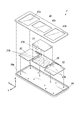
- FIG. 1 is an exploded perspective view of the RFID tag according to the first embodiment of the present disclosure.
- the RFID tag 1 of the first embodiment includes a housing 10, a circuit board 20, a photovoltaic panel 31, 32, a display 33, and a lid 40.
- the display 33 corresponds to an example of the first function module according to the present disclosure.
- the photovoltaic power generation panels 31 and 32 correspond to an example of the second function module and the third function module according to the present disclosure.
- the housing 10 has a concave shape in which one side is open, and the circuit board 20 and the display 33 can be overlapped with each other, and two photovoltaic panels 31 and 32 can be accommodated side by side on the left and right sides of the display 33.
- the housing 10 includes ABS (acrylonitrile, butadiene, styrene resin), PC (polycarbonate), POM (polyacetyl), PP (polypropylene), PPS (polyphenylene terephite), PA (polyethylene), EVA (ethylene vinyl acetate copolymerization).
- PE polyethylene
- PBT polybutylene terephthalate
- PS polystyrene
- EP epoxy resin
- PF phenol resin
- the housing 10 may be formed of a mixed material containing any of the above materials as a main material and a mixture of other materials, or may be formed of a material containing an inorganic filler.
- the display 33 is, for example, a liquid crystal display panel, and is electrically connected to the circuit board 20 via wiring (film wiring or the like) 33h.
- the photovoltaic panels 31 and 32 receive light from the outside to generate electricity.
- Each of the display 33 and the photovoltaic panels 31 and 32 may have a rectangular plate shape.
- the photovoltaic power generation panels 31 and 32 are electrically connected to the circuit board 20 via wirings (lead wires and the like) 31h and 32h.
- the wirings 31h to 33h may be detachably connected to each other on the circuit board 20 via a connector.
- the lid 40 has transparent windows 41a to 41c in a range facing the photovoltaic panels 31, 32 and the display 33, and is joined to the inner frame 10a of the housing 10 to seal the inside of the housing 10.
- FIG. 2 is a block diagram showing a circuit configuration of the RFID tag of the first embodiment.
- the RFID tag 1 includes a PMIC (Power Management Integrated Circuit) 21 that inputs generated power from the photovoltaic panels 31 and 32 to manage the power, and a first power supply IC 22 that receives power from the PMIC 21 to generate a power supply voltage for the control system.
- a second power supply IC 23 that receives power from the PMIC 21 and generates a drive voltage for the display 33.
- the RFID tag 1 includes an RFID IC 25 that wirelessly communicates with a reader / writer via radio waves, and a control circuit 24 that communicates with the RFID IC 25 and controls the display of the display 33.
- the control circuit 24 and the RFID IC 25 operate by receiving a power supply voltage from the first power supply IC 22.
- the RFID IC 25 performs wireless communication using, for example, UHF (Ultra High Frequency) band radio waves.
- the RFID IC 25 has a storage unit that can be read and written from a reader / writer, and identification information, management information, and the like are stored in the storage unit.
- the control circuit 24 is, for example, a microcomputer, and can communicate with the RFID IC 25 to read information from the storage unit of the RFID IC 25.
- the control circuit 24 controls the display content of the display 33 based on the read information.
- the PMIC 21, the first power supply IC 22, the second power supply IC 23, the control circuit 24, and the RFID IC 25 are mounted on the circuit board 20.
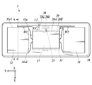
- FIG. 3 is a plan view of a configuration in which a circuit board and a functional module are mounted on a housing.
- the display 33 is represented by a two-dot chain line.
- the circuit board 20 includes a main portion 20A extending in the XY direction and an extending portion 20B extending along the upper side (edge portion) of the main portion 20A and extending long on both sides of the main portion 20A in the X direction. Has. That is, one end and the other end of the extending portion 20B in the longitudinal direction protrude from one and the other along the upper side of the main portion 20A rather than the main portion 20A.
- the boundary line E1 shows a virtual boundary between the main portion 20A and the extending portion 20B.
- the plane of the main portion 20A may be rectangular.
- the main part 20A includes the ground surface 27.
- the ground surface 27 is formed on one surface or an intermediate layer of the circuit board 20 and occupies most of the main portion 20A in the direction along the XY plane. In FIG. 3, the ground surface 27 is formed on the back surface (rear surface) of the circuit board 20, and is indicated by a broken line.
- the main unit 20A has mounting surfaces such as a control circuit 24, a PMIC 21, a first power supply IC 22, a second power supply IC 23, a display panel connection connector, and a photovoltaic power generation panel connector, and these components are mounted. These are mounted on the back side (rear surface, rear surface) of the circuit board 20 of FIG. 3, and are not shown in FIG.
- the RFID IC 25 If the RFID IC 25 is connected to the antenna conductor 28 in the vicinity of the boundary between the main portion 20A and the extending portion 20B, it may be mounted on the main portion 20A or the extending portion 20B. It may be mounted on these boundaries.
- the width of the main portion 20A may be substantially the same as that of the display 33.
- the extending portion 20B includes the antenna conductor 28 and is integrated with the main portion 20A.
- the antenna conductor 28 is formed on one surface of the circuit board 20 (for example, the rear surface in FIG. 3).
- the electromagnetic field radiated from the antenna conductor 28 is radiated in all directions on the YZ plane perpendicular to the longitudinal direction (X direction) of the antenna conductor 28.
- the antenna conductor 28 may be formed in the intermediate layer of the circuit board 20.
- the antenna conductor 28 includes a band-shaped portion 28a for radio wave radiation having a length that resonates at the frequency of the radio signal, and a pattern portion 28b for impedance matching.
- the strip 28a may extend to the range in which the photovoltaic panels 31 and 32 are arranged in the X direction.
- the band-shaped portion 28a is longer than the width of the main portion 20A and the ground surface 27, and extends longer than the main portion 20A and the ground surface 27 in one and the other in the X direction.
- the band-shaped portion 28a may form a dipole antenna whose electrical length is approximately half the wavelength of the radio signal of the RFID IC 25.
- the minimum distance L1 between the band-shaped portion 28a and the ground surface 27 is longer than the width L2 of the strip-shaped portion 28a in the lateral direction.
- the pattern portion 28b has, for example, a loop-shaped pattern, is provided between the band-shaped portion 28a and the feeding point of the RFID IC 25, and matches the impedance between the two.
- the display 33 overlaps the main portion 20A of the circuit board 20 in the Z direction, and does not overlap the extending portion 20B in the Z direction.
- the display 33 may overlap a part of the pattern portion 28b and the extending portion 20B as long as it does not overlap the strip-shaped portion 28a of the antenna conductor 28.
- the photovoltaic power generation panels 31 and 32 are arranged on both side portions W1 and W2 that are partitioned by the main portion 20A and the extending portion 20B of the circuit board 20.
- one corner 31a of the photovoltaic power generation panel 31 fits in the side portion W1, and the two sides 31e1 and 31e2 of the photovoltaic power generation panel 31 form the lower side of the extending portion 20B and the left side of the main portion 20A that partition the two sides. Along with each. The same applies to the other photovoltaic panel 32.
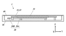
- FIG. 4 is a vertical sectional view showing the RFID tag of the first embodiment.
- FIG. 4 shows a cross section at the position of the arrow AA in FIG.
- the display 33 is shown by a virtual line.
- the display 33 and the circuit board 20 are arranged so as to overlap each other in the Z direction.
- the photovoltaic power generation panels 31 and 32 are arranged so as to overlap the display 33 when viewed in the direction along the XY plane, and are arranged so as not to overlap the circuit board 20.
- the photovoltaic power generation panels 31 and 32 may be arranged at a height that does not overlap with the display 33 when viewed in a direction along the XY plane, or may be arranged at a height that overlaps with the circuit board 20. You may.
- 5A and 5B are diagrams showing a simulation configuration and antenna characteristics of the RFID tag of the first embodiment.
- 6A and 6B are diagrams showing a simulation configuration and antenna characteristics of an RFID tag of a comparative example.
- the antenna conductor 28 and the ground surface 27 are shown by fine solid lines for easy viewing.
- the antenna conductor 828 and the ground surface 827 are shown by fine solid lines in a range that does not overlap with the photovoltaic panels 31 and 32 for easy viewing.
- the + Z direction of FIG. 5A corresponds to 0 ° of the XZ plane radiation pattern and the YZ plane radiation pattern
- the ⁇ X direction of FIG. 5A corresponds to ⁇ 90 ° of the XZ plane radiation pattern
- the ⁇ 90 ° of FIG. 5A corresponds to ⁇ 90 ° of the YZ plane radiation pattern.
- the antenna radiation characteristics were simulated with the length of the antenna conductor 28 being 114 mm and the width of the ground surface 27 being 59.4 mm.
- a high value (1.6 dBi) was obtained as the antenna gain in the Z direction (0 ° direction).
- a good value (at least 0.4 dBi) independent of the direction was obtained as the antenna gain on the YZ plane.
- the antenna gain in the Z direction (0 ° direction) was as low as -5.8 dBi. Further, the value of the antenna gain on the YZ plane in the ⁇ Y direction ( ⁇ 90 ° direction) was high, and the value in the Y direction (90 ° direction) was very low.
- the length of the antenna conductor 828 is 114 mm
- the width of the main portion 820A of the circuit board 820 matches the width of the extending portion 820B
- the width of the ground surface 827 matches the length of the antenna conductor 828. This is an example in which the elements are configured in the same manner as in FIG. 5A of the first embodiment.
- a strong electric field appears at the ends of the antenna conductors 28 and 828.
- the ground surfaces 27 and 827 have one surface that acts as a reflector for radio waves.
- the ground surface 827 acting as a reflector near the end of the antenna conductor 828 where a strong electric field is generated causes directivity in the antenna gain on the YZ surface, and also Z.
- the antenna gain in the direction is reduced.
- the ground surface 27 acting as a reflector is separated from the end of the antenna conductor 28 where a strong electric field is generated, so that the YZ surface radiation characteristic becomes uniform regardless of the direction.
- the antenna gain in the Z direction is improved.
- the extending portion 20B of the circuit board 20 and the antenna conductor 28 are formed along the upper side (edge portion) of the main portion 20A of the circuit board 20. And it extends longer than the ground surface 27. Therefore, since the end portion of the antenna conductor 28 in which a strong electric field is generated is separated from the ground surface 27, it is possible to prevent the electric field of the radio signal from being concentrated between the end portion and the ground surface 27. Further, the decrease of the antenna gain in the specific direction (Z direction) due to the ground surface 27 acting as a reflector is suppressed. As a result, the antenna gain can be improved, and the antenna characteristics (characteristics in which the antenna gain is high in the direction of the display surface) suitable for the RFID tag 1 with a display function can be obtained.
- the extending portion 20B and the antenna conductor 28 extend to both the left and right sides longer than the main portion 20A of the circuit board 20. Therefore, both ends of the antenna conductor 28 can be separated from the ground surface 27. Therefore, the antenna gain can be further improved, and more suitable antenna characteristics can be obtained.
- This configuration is particularly effective for an antenna conductor 28 in which a strong electric field is generated at both ends, such as a dipole antenna.
- the antenna conductor 28 includes the band-shaped portion 28a for radio wave radiation, and the minimum distance L1 between the band-shaped portion 28a and the ground surface 27 is the width of the band-shaped portion 28a in the lateral direction. It is larger than L2 (Fig. 3).
- L1 between the band-shaped portion 28a and the ground surface 27
- L2 Fig. 3
- the photovoltaic power generation panels 31 and 32 are arranged on the side portions W1 and W2 in which the main portion 20A and the extending portion 20B of the circuit board 20 are partitioned. .. With such a configuration, it is possible to secure an effective arrangement space for the photovoltaic power generation panels 31 and 32 while preventing the photovoltaic power generation panels 31 and 32 from overlapping with the antenna conductor 28 in the front-rear direction.
- the display 33 overlaps the main portion 20A of the circuit board 20, and the two photovoltaic panels 31 and 32 are arranged on both side portions W1 and W2.
- the display 33 and the two photovoltaic panels 31 and 32 can be arranged side by side in a row within the limited space of the housing 10, and the antenna conductor 28 can be arranged with these. Good antenna characteristics can be obtained without overlapping in the front-back direction.
- FIG. 7A and 7B are a plan view showing the RFID tag of the second embodiment and a plan view of a circuit board.
- the display 33 is represented by a virtual line, and the lid 40 is not shown.
- the RFID tag 101 of the second embodiment has a different shape of the extending portion 120B of the circuit board 120 and the antenna conductor 128, while the other components are substantially the same as those of the first embodiment. Similar components are designated by the same reference numerals as those in the first embodiment, and detailed description thereof will be omitted.
- the circuit board 120 has a main portion 20A extending in the XY direction and an extending portion extending along the left side, the upper side, and the right side (left edge portion, upper edge portion, and right edge portion) of the main portion 20A. It has 120B and.
- the boundary line E2 represents a virtual boundary between the main portion 20A and the extending portion 120B.
- the extending portion 120B is above the display 33, to the left of the display 33 (between the display 33 and the photovoltaic panel 31), and to the right of the display 33 (display).
- the main portion 20A includes the ground surface 27 as in the first embodiment, and is mounted with the same parts as those in the first embodiment.
- the extending portion 120B includes the antenna conductor 128 and is integrated with the main portion 20A.
- the antenna conductor 128 includes a band-shaped portion 128a for radio wave radiation having a length that resonates at the frequency of the radio signal, and a pattern portion 28b for impedance matching.
- the pattern portion 28b is the same as that of the first embodiment.
- the band-shaped portion 128a is a first extending in the Y direction between the central strip-shaped portion 128a0 extending in the X direction above the main portion 20A and the display 33 and the photovoltaic power generation panel 31 when viewed in the Z direction. It includes a strip-shaped portion 128a1 and a second strip-shaped portion 128a2 extending in the Y direction between the display 33 and the photovoltaic power generation panel 32 when viewed in the Z direction.
- the band-shaped portion 128a may form a dipole antenna whose electrical length is approximately half the wavelength of the radio signal of the RFID IC 25.
- the minimum distance L1 between the central strip-shaped portion 128a0 and the ground surface 27 is larger than the width L2 of the central strip-shaped portion 128a0 in the lateral direction.
- the minimum distance L3 between the first band-shaped portion 128a1 and the ground surface 27 is larger than the width L4 of the first strip-shaped portion 128a1 in the lateral direction.
- the minimum distance L5 between the second strip portion 128a2 and the ground surface 27 is larger than the width L6 of the second strip portion 128a2 in the lateral direction.
- FIG. 8A and 8B are diagrams showing a simulation configuration and antenna characteristics of the RFID tag of the second embodiment.
- the antenna conductor 128 and the ground surface 27 are shown by fine solid lines for easy viewing.
- the + Z direction of FIG. 8A corresponds to 0 ° of the XZ plane radiation pattern and the YZ plane radiation pattern
- the ⁇ X direction of FIG. 8A corresponds to ⁇ 90 ° of the XZ plane radiation pattern
- the ⁇ 90 ° of FIG. 8A The Y direction corresponds to ⁇ 90 ° of the YZ plane radiation pattern.
- the minimum distances L3 and L5 between the first strip 128a1 and the second strip 128a2 and the ground surface 27 are 6 mm, and the width of the strip 128a in the lateral direction.
- the antenna radiation characteristics were simulated with a value of 1.2 mm.
- a higher value (0.5 dBi) was obtained as the antenna gain in the Z direction (0 °) as compared with the comparative examples of FIGS. 6A and 6B, and further, in the ⁇ X direction as well.
- a certain amount of antenna gain (-10 dBi) was obtained.
- a good value (0 to 2 dBi) independent of the direction was obtained as the antenna gain on the YZ plane.
- the antenna gain in the ⁇ X direction is increased as compared with the first embodiment due to the presence of the first band-shaped portion 128a1 and the second band-shaped portion 128a2 extending in the Y direction. .. Further, since the end of the antenna conductor 128 where a strong electric field is generated is far away from the ground surface 27, the electric field is not concentrated between the end and the ground surface 27, and a decrease in antenna gain is avoided. There is. In addition, since the ground surface 27 acts as a reflector on the first band-shaped portion 128a1 of the antenna conductor 128, the antenna gain in the ⁇ X direction increases, and the ground surface 27 reflects on the second band-shaped portion 128a2. By acting as a vessel, the antenna gain in the X direction is increased. As a result, the antenna characteristics approach omnidirectional even on the XZ surface, and radiation characteristics suitable for RFID tags are obtained.
- the extending portion 120B of the circuit board 120 and the antenna conductor 128 are viewed in the Z direction in addition to the upper side (edge portion) of the main portion 20A. Therefore, it extends between the display 33 and the two photovoltaic panels 31 and 32.
- the display 33 and the two photovoltaic panels 31 and 32 can be arranged in a row, and the antenna conductor 28 does not overlap with them in the front-rear direction to obtain good antenna characteristics. be able to.
- the antenna conductor 28 since the antenna conductor 28 includes a portion extending in the X direction and a portion extending in the Y direction, the antenna characteristics on the XZ plane can be made omnidirectional as compared with the configuration of the first embodiment. it can.
- the minimum distance L3 between the first band-shaped portion 128a1 of the antenna conductor 28 and the ground surface 27 is larger than the width L4 in the lateral direction of the first band-shaped portion 128a1. Large (Fig. 7A).
- the minimum distance L5 between the second band-shaped portion 128a2 and the ground surface 27 is larger than the width L6 of the second strip-shaped portion 128a2 in the lateral direction (FIG. 7A).
- the action of the ground surface 27 as a reflector works in a direction of improving the antenna gain with respect to the radio waves in the ⁇ X direction, and the antenna characteristics on the XZ surface can be made closer to omnidirectional.
- the present invention is not limited to the above embodiment.
- functional modules include temperature, humidity, illuminance, vibration, acceleration, and the like.
- Various modules such as a sensor module, a sound collector, and a loudspeaker for detecting the above may be applied.
- the details shown in the embodiment can be appropriately changed without departing from the spirit of the invention.
- This disclosure can be used for RFID tags equipped with a plurality of functional modules.
Landscapes
- Engineering & Computer Science (AREA)
- Computer Hardware Design (AREA)
- Microelectronics & Electronic Packaging (AREA)
- Physics & Mathematics (AREA)
- General Physics & Mathematics (AREA)
- Theoretical Computer Science (AREA)
- Computer Networks & Wireless Communication (AREA)
- Sustainable Development (AREA)
- Life Sciences & Earth Sciences (AREA)
- Sustainable Energy (AREA)
- Electromagnetism (AREA)
- Details Of Aerials (AREA)
- Variable-Direction Aerials And Aerial Arrays (AREA)
Priority Applications (4)
| Application Number | Priority Date | Filing Date | Title |
|---|---|---|---|
| US17/442,719 US11763123B2 (en) | 2019-03-26 | 2020-03-17 | RFID tag |
| EP20776893.8A EP3951659A4 (en) | 2019-03-26 | 2020-03-17 | RFID LABEL |
| JP2021509109A JP7238098B2 (ja) | 2019-03-26 | 2020-03-17 | Rfidタグ |
| CN202080023686.XA CN113614742A (zh) | 2019-03-26 | 2020-03-17 | Rfid标签 |
Applications Claiming Priority (2)
| Application Number | Priority Date | Filing Date | Title |
|---|---|---|---|
| JP2019-058550 | 2019-03-26 | ||
| JP2019058550 | 2019-03-26 |
Publications (1)
| Publication Number | Publication Date |
|---|---|
| WO2020196067A1 true WO2020196067A1 (ja) | 2020-10-01 |
Family
ID=72609784
Family Applications (1)
| Application Number | Title | Priority Date | Filing Date |
|---|---|---|---|
| PCT/JP2020/011579 Ceased WO2020196067A1 (ja) | 2019-03-26 | 2020-03-17 | Rfidタグ |
Country Status (5)
| Country | Link |
|---|---|
| US (1) | US11763123B2 (https=) |
| EP (1) | EP3951659A4 (https=) |
| JP (1) | JP7238098B2 (https=) |
| CN (1) | CN113614742A (https=) |
| WO (1) | WO2020196067A1 (https=) |
Families Citing this family (1)
| Publication number | Priority date | Publication date | Assignee | Title |
|---|---|---|---|---|
| WO2021216887A1 (en) * | 2020-04-22 | 2021-10-28 | Biotags, LLC | Temperature sensor patch and system |
Citations (4)
| Publication number | Priority date | Publication date | Assignee | Title |
|---|---|---|---|---|
| JP2002065418A (ja) | 2000-08-30 | 2002-03-05 | Hitachi Cable Ltd | 商品情報表示システム及び商品情報表示媒体 |
| JP2014095939A (ja) * | 2012-11-07 | 2014-05-22 | Toppan Forms Co Ltd | 情報表示媒体 |
| JP2017072939A (ja) * | 2015-10-06 | 2017-04-13 | 凸版印刷株式会社 | 電子デバイス及び収容体 |
| JP2018190351A (ja) * | 2017-05-11 | 2018-11-29 | トッパン・フォームズ株式会社 | 非接触型データ受送信体 |
Family Cites Families (15)
| Publication number | Priority date | Publication date | Assignee | Title |
|---|---|---|---|---|
| US8044800B2 (en) | 2006-11-14 | 2011-10-25 | Semiconductor Energy Laboratory Co., Ltd. | Semiconductor device |
| US20090085750A1 (en) * | 2007-09-27 | 2009-04-02 | 3M Innovative Properties Company | Extended RFID tag |
| US8098161B2 (en) | 2008-12-01 | 2012-01-17 | Raytheon Company | Radio frequency identification inlay with improved readability |
| US9918537B2 (en) * | 2009-04-01 | 2018-03-20 | Vanguard Identification Systems | Smart device programmable electronic luggage tag and bag mountings therefore |
| KR101607131B1 (ko) * | 2009-08-17 | 2016-03-30 | 삼성전자주식회사 | 휴대용 단말기의 다중 대역 내장형 안테나 장치 |
| JP5403353B2 (ja) * | 2009-11-11 | 2014-01-29 | 日立化成株式会社 | Rfidタグの製造方法 |
| JP6016013B2 (ja) * | 2012-07-10 | 2016-10-26 | 日立化成株式会社 | Rfidタグ及び自動認識システム |
| JP2013070420A (ja) * | 2012-11-30 | 2013-04-18 | Fujifilm Corp | Rfidタグ、非接触通信装置、非接触通信方法、及び非接触通信システム |
| JP6455199B2 (ja) | 2015-02-09 | 2019-01-23 | 凸版印刷株式会社 | 表示機能付き電子デバイス及びカバン物品 |
| US9863914B2 (en) * | 2015-07-24 | 2018-01-09 | Implant Sciences Corporation | Miniature quadrupole arrays using electron multiplication detectors |
| US10921979B2 (en) * | 2015-12-07 | 2021-02-16 | Huawei Technologies Co., Ltd. | Display and processing methods and related apparatus |
| WO2018101379A1 (ja) * | 2016-12-02 | 2018-06-07 | 株式会社村田製作所 | Rfidタグ付き包装袋および包装袋の開封管理システム、並びに、rfidタグ付き貼付シートおよび貼付シートを貼付した容器の開封管理システム |
| WO2018199007A1 (ja) * | 2017-04-28 | 2018-11-01 | 株式会社村田製作所 | Rfidタグ |
| KR102426656B1 (ko) * | 2017-11-28 | 2022-07-28 | 삼성전자주식회사 | 안테나를 포함하는 전자 장치 |
| CN107977586B (zh) * | 2017-12-22 | 2021-04-13 | 联想(北京)有限公司 | 显示内容处理方法、第一电子设备以及第二电子设备 |
-
2020
- 2020-03-17 CN CN202080023686.XA patent/CN113614742A/zh active Pending
- 2020-03-17 WO PCT/JP2020/011579 patent/WO2020196067A1/ja not_active Ceased
- 2020-03-17 US US17/442,719 patent/US11763123B2/en active Active
- 2020-03-17 JP JP2021509109A patent/JP7238098B2/ja active Active
- 2020-03-17 EP EP20776893.8A patent/EP3951659A4/en not_active Withdrawn
Patent Citations (4)
| Publication number | Priority date | Publication date | Assignee | Title |
|---|---|---|---|---|
| JP2002065418A (ja) | 2000-08-30 | 2002-03-05 | Hitachi Cable Ltd | 商品情報表示システム及び商品情報表示媒体 |
| JP2014095939A (ja) * | 2012-11-07 | 2014-05-22 | Toppan Forms Co Ltd | 情報表示媒体 |
| JP2017072939A (ja) * | 2015-10-06 | 2017-04-13 | 凸版印刷株式会社 | 電子デバイス及び収容体 |
| JP2018190351A (ja) * | 2017-05-11 | 2018-11-29 | トッパン・フォームズ株式会社 | 非接触型データ受送信体 |
Also Published As
| Publication number | Publication date |
|---|---|
| JPWO2020196067A1 (https=) | 2020-10-01 |
| US20220188590A1 (en) | 2022-06-16 |
| JP7238098B2 (ja) | 2023-03-13 |
| CN113614742A (zh) | 2021-11-05 |
| US11763123B2 (en) | 2023-09-19 |
| EP3951659A4 (en) | 2023-01-04 |
| EP3951659A1 (en) | 2022-02-09 |
Similar Documents
| Publication | Publication Date | Title |
|---|---|---|
| US12199332B2 (en) | Antenna device for vehicle | |
| CN102742078B (zh) | 无线机 | |
| US10790588B2 (en) | Loop antenna and electronic device | |
| JP2022093405A (ja) | Rfidタグ | |
| JP2005135354A (ja) | 無線タグ読取り装置及びこの装置に使用する無線タグモジュール並びに無線タグ付き物品及びこの物品を収納する収納箱 | |
| CN118232026A (zh) | 一种天线结构和电子设备 | |
| JP7238098B2 (ja) | Rfidタグ | |
| US12531344B2 (en) | Antenna device and communication device | |
| CN114600315B (zh) | 双极化天线模块及包括所述天线模块的电子设备 | |
| JP7782156B2 (ja) | 車両用無線装置 | |
| JP2018085703A (ja) | 線状アンテナ及び電子機器 | |
| US8228249B2 (en) | In-vehicle antenna device | |
| JP4417931B2 (ja) | 無線タグ読取装置及び読取方法 | |
| US12347945B2 (en) | Wireless communication device | |
| JP7060764B2 (ja) | Rfidタグ | |
| JPWO2017038549A1 (ja) | アンテナ構造及び電子機器 | |
| WO2020262126A1 (ja) | Rfidタグ | |
| US20220253662A1 (en) | Rfid tag | |
| US12261379B2 (en) | Antenna device | |
| US20260039013A1 (en) | Antenna device | |
| JP2007018518A (ja) | 無線タグ読取り装置 |
Legal Events
| Date | Code | Title | Description |
|---|---|---|---|
| 121 | Ep: the epo has been informed by wipo that ep was designated in this application |
Ref document number: 20776893 Country of ref document: EP Kind code of ref document: A1 |
|
| ENP | Entry into the national phase |
Ref document number: 2021509109 Country of ref document: JP Kind code of ref document: A |
|
| NENP | Non-entry into the national phase |
Ref country code: DE |
|
| ENP | Entry into the national phase |
Ref document number: 2020776893 Country of ref document: EP Effective date: 20211026 |