WO2020195885A1 - 半導体装置および半導体装置の製造方法 - Google Patents
半導体装置および半導体装置の製造方法 Download PDFInfo
- Publication number
- WO2020195885A1 WO2020195885A1 PCT/JP2020/010764 JP2020010764W WO2020195885A1 WO 2020195885 A1 WO2020195885 A1 WO 2020195885A1 JP 2020010764 W JP2020010764 W JP 2020010764W WO 2020195885 A1 WO2020195885 A1 WO 2020195885A1
- Authority
- WO
- WIPO (PCT)
- Prior art keywords
- pad
- region
- semiconductor device
- metal
- layer
- Prior art date
- Legal status (The legal status is an assumption and is not a legal conclusion. Google has not performed a legal analysis and makes no representation as to the accuracy of the status listed.)
- Ceased
Links
Images








Classifications
-
- H—ELECTRICITY
- H10—SEMICONDUCTOR DEVICES; ELECTRIC SOLID-STATE DEVICES NOT OTHERWISE PROVIDED FOR
- H10F—INORGANIC SEMICONDUCTOR DEVICES SENSITIVE TO INFRARED RADIATION, LIGHT, ELECTROMAGNETIC RADIATION OF SHORTER WAVELENGTH OR CORPUSCULAR RADIATION
- H10F39/00—Integrated devices, or assemblies of multiple devices, comprising at least one element covered by group H10F30/00, e.g. radiation detectors comprising photodiode arrays
- H10F39/10—Integrated devices
- H10F39/12—Image sensors
-
- H—ELECTRICITY
- H10—SEMICONDUCTOR DEVICES; ELECTRIC SOLID-STATE DEVICES NOT OTHERWISE PROVIDED FOR
- H10P—GENERIC PROCESSES OR APPARATUS FOR THE MANUFACTURE OR TREATMENT OF DEVICES COVERED BY CLASS H10
- H10P14/00—Formation of materials, e.g. in the shape of layers or pillars
- H10P14/40—Formation of materials, e.g. in the shape of layers or pillars of conductive or resistive materials
-
- H—ELECTRICITY
- H10—SEMICONDUCTOR DEVICES; ELECTRIC SOLID-STATE DEVICES NOT OTHERWISE PROVIDED FOR
- H10W—GENERIC PACKAGES, INTERCONNECTIONS, CONNECTORS OR OTHER CONSTRUCTIONAL DETAILS OF DEVICES COVERED BY CLASS H10
- H10W20/00—Interconnections in chips, wafers or substrates
- H10W20/01—Manufacture or treatment
-
- H—ELECTRICITY
- H10—SEMICONDUCTOR DEVICES; ELECTRIC SOLID-STATE DEVICES NOT OTHERWISE PROVIDED FOR
- H10W—GENERIC PACKAGES, INTERCONNECTIONS, CONNECTORS OR OTHER CONSTRUCTIONAL DETAILS OF DEVICES COVERED BY CLASS H10
- H10W20/00—Interconnections in chips, wafers or substrates
- H10W20/40—Interconnections external to wafers or substrates, e.g. back-end-of-line [BEOL] metallisations or vias connecting to gate electrodes
-
- H—ELECTRICITY
- H10—SEMICONDUCTOR DEVICES; ELECTRIC SOLID-STATE DEVICES NOT OTHERWISE PROVIDED FOR
- H10W—GENERIC PACKAGES, INTERCONNECTIONS, CONNECTORS OR OTHER CONSTRUCTIONAL DETAILS OF DEVICES COVERED BY CLASS H10
- H10W72/00—Interconnections or connectors in packages
- H10W72/50—Bond wires
- H10W72/531—Shapes of wire connectors
- H10W72/536—Shapes of wire connectors the connected ends being ball-shaped
-
- H—ELECTRICITY
- H10—SEMICONDUCTOR DEVICES; ELECTRIC SOLID-STATE DEVICES NOT OTHERWISE PROVIDED FOR
- H10W—GENERIC PACKAGES, INTERCONNECTIONS, CONNECTORS OR OTHER CONSTRUCTIONAL DETAILS OF DEVICES COVERED BY CLASS H10
- H10W72/00—Interconnections or connectors in packages
- H10W72/50—Bond wires
- H10W72/531—Shapes of wire connectors
- H10W72/5363—Shapes of wire connectors the connected ends being wedge-shaped
-
- H—ELECTRICITY
- H10—SEMICONDUCTOR DEVICES; ELECTRIC SOLID-STATE DEVICES NOT OTHERWISE PROVIDED FOR
- H10W—GENERIC PACKAGES, INTERCONNECTIONS, CONNECTORS OR OTHER CONSTRUCTIONAL DETAILS OF DEVICES COVERED BY CLASS H10
- H10W72/00—Interconnections or connectors in packages
- H10W72/90—Bond pads, in general
-
- H—ELECTRICITY
- H10—SEMICONDUCTOR DEVICES; ELECTRIC SOLID-STATE DEVICES NOT OTHERWISE PROVIDED FOR
- H10W—GENERIC PACKAGES, INTERCONNECTIONS, CONNECTORS OR OTHER CONSTRUCTIONAL DETAILS OF DEVICES COVERED BY CLASS H10
- H10W72/00—Interconnections or connectors in packages
- H10W72/90—Bond pads, in general
- H10W72/931—Shapes of bond pads
- H10W72/932—Plan-view shape, i.e. in top view
-
- H—ELECTRICITY
- H10—SEMICONDUCTOR DEVICES; ELECTRIC SOLID-STATE DEVICES NOT OTHERWISE PROVIDED FOR
- H10W—GENERIC PACKAGES, INTERCONNECTIONS, CONNECTORS OR OTHER CONSTRUCTIONAL DETAILS OF DEVICES COVERED BY CLASS H10
- H10W90/00—Package configurations
- H10W90/701—Package configurations characterised by the relative positions of pads or connectors relative to package parts
- H10W90/751—Package configurations characterised by the relative positions of pads or connectors relative to package parts of bond wires
- H10W90/754—Package configurations characterised by the relative positions of pads or connectors relative to package parts of bond wires between a chip and a stacked insulating package substrate, interposer or RDL
Definitions
- the present disclosure relates to a semiconductor device and a method for manufacturing the semiconductor device. More specifically, the present invention relates to a semiconductor device in which a pad is arranged on the surface of a semiconductor chip and a method for manufacturing the semiconductor device.
- a semiconductor device configured by arranging pads on the surface of a semiconductor chip.
- This pad is an electrode for extracting a signal to the outside of the semiconductor chip.
- a bonding wire is connected to the pad by wire bonding, and a signal is transmitted through the bonding wire.
- a gold (Au) wire or the like is used as a bonding wire and welded to a pad to obtain an electrical connection.
- the welding of the bonding wire can be performed by heat-pressing the bonding wire having a spherical tip to the pad.
- the semiconductor chip may be damaged during this wire bonding. For example, the impact of wire bonding may damage the interlayer insulating film directly under the pad and cause cracks.
- Patent Document 1 a semiconductor device in which a tungsten structure, which is a high-hardness structure, is arranged in an insulating layer directly under the pad.
- This tungsten structure has a structure in which a plurality of plates having a constant length and a constant width are juxtaposed at regular intervals.
- the present disclosure has been made in view of the above-mentioned problems, and an object of the present disclosure is to simplify the configuration of a pad of a semiconductor device.
- the present disclosure has been made to solve the above-mentioned problems, and the first aspect thereof is that the metal region and the bulging region where the deformed portion bulges when the metal region is deformed are in the same layer.
- This is a semiconductor device including a pad in which a mixed pad layer, which is a pad layer arranged in a semiconductor substrate, is arranged adjacent to an interlayer insulating film formed on a semiconductor substrate.
- the bulging region may be composed of a member having a cavity inside.
- the bulging region may be composed of the member having the cavity formed inside by closing the top of the opening formed in the metal film.
- the opening of the metal film may have a reverse tapered cross section.
- the opening of the metal film may be configured to have a height of 1.5 times or more the width of the cross section.
- the bulging region may be composed of voids.
- the pad may be configured by laminating a plurality of pad layers including at least one of the hybrid pad layers.
- the pad may include a pad layer composed of metal regions having different Young's modulus.
- the metal regions may be arranged at a ratio of 0.5 or more in the hybrid pad layer.
- the metal region of the hybrid pad layer may be connected to the wiring layer by a via plug.
- the pad may be a pad for wire bonding.
- the pad may be a pad to which the inspection probe is abutted.
- a second aspect of the present disclosure is the metal region of a mixed pad layer, which is a pad layer in which a metal region and a bulging region in which the deformed portion bulges when the metal region is deformed are arranged in the same layer.
- the metal region arrangement step of arranging the metal region adjacent to the interlayer insulating film formed on the semiconductor substrate This is a method for manufacturing a semiconductor device including a bulge region arranging step of arranging the bulge region in the same layer as the formed metal region.
- the metal region of the pad layer constituting the pad bulges into the adjacent bulging region, and the metal region is deformed in the direction parallel to the pad layer. It is assumed that the deformation of the metal region in the direction perpendicular to the pad layer is suppressed.
- FIG. 1 is a diagram showing a configuration example of a semiconductor device according to the embodiment of the present disclosure.
- FIG. 6 is a diagram showing a state in which a semiconductor chip-shaped semiconductor device 100 is mounted on a substrate 10.
- the pad 200 is an electrode that transmits a signal when exchanging a signal with an external device of the semiconductor device 100.
- the pad 11 is also arranged on the substrate 10. After the semiconductor device 100 is die-bonded to the substrate 10, the pad 200 of the semiconductor device 100 and the pad 11 of the substrate 10 are connected one-to-one by the bonding wire 20.
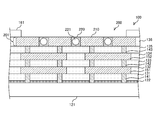
- FIG. 2 is a diagram showing a configuration example of a pad according to the first embodiment of the present disclosure.
- FIG. 6 is a plan view showing a configuration example of the pad 200.
- the pad 200 in the figure is configured by arranging a metal region 210 and a bulging region 220 in a striped pattern.
- the metal region 210 is a conductor that transmits a signal.
- the metal region 210 is made of a metal such as copper (Cu) and is connected to a wiring described later.
- a bonding wire is connected to the metal region 210 to transmit an electric signal.
- the bulging region 220 is arranged adjacent to the metal region 210, and is a region in which the deformed portion bulges when the metal region 210 is deformed.
- the bulging region 220 in the figure can be composed of, for example, an insulating material having a cavity inside.
- the metal region 210 is compressed and deformed during wire bonding. As a result, a part of the metal constituting the metal region 210 bulges. That is, a part of the metal protrudes from the region of the metal region 210 before deformation.
- the bulging region 220 is a region for bulging the deformed metal region 210, which is the protruding portion. By arranging the bulging region 220, bulging to the lower layer of the metal region 210 can be prevented. Details of the bulge of the metal region 210 will be described later.
- FIG. 3 is a cross-sectional view showing a configuration example of the pad according to the first embodiment of the present disclosure.
- FIG. 6 is a cross-sectional view showing a configuration example of a portion of the pad 200 of the semiconductor device 100.
- the semiconductor device 100 includes a semiconductor substrate 121, an insulating film 122, an interlayer insulating films 131 to 136, wiring layers 151 and 152, a contact plug 141, via plugs 142 and 143, a protective film 161 and a pad 200. Be prepared.
- the semiconductor substrate 121 is a semiconductor substrate on which a semiconductor portion (diffusion region) of an element arranged in the semiconductor device 100 is formed.
- a semiconductor substrate for example, a substrate made of silicon (Si) can be used.
- Si silicon
- the insulating film 122 insulates the surface of the semiconductor substrate 121.
- the insulating film 122 is made of silicon oxide (SiO 2 ) or silicon nitride (SiN) to insulate and protect the surface of the semiconductor substrate 121.
- the wiring layers 151 and 152 are wirings that transmit signals to the diffusion layer and the pad 200 of the semiconductor substrate 121.
- the wiring layers 151 and 152 can be made of, for example, a metal such as Cu. Further, the wiring layers 151 and 152 are arranged in different layers.
- the interlayer insulating films 131 to 136 insulate the wiring layers 151 and 152 and the like. These wiring layers 151 and 152 and the interlayer insulating films 131 to 136 form a wiring region.
- the figure shows an example of a wiring region having a two-layer structure.
- the contact plug 141 connects the diffusion layer and the wiring layer 151 of the semiconductor substrate 121. Further, the via plug 142 connects the wiring layers 151 and 152. The via plug 143 connects the wiring layer 152 and the metal region 210 of the pad 200.
- These contact plugs 141 and via plugs 142 and 143 are made of columnar metal, and wiring layers and the like arranged in different layers can be connected.
- the contact plug 141 and the via plugs 142 and 143 can be made of, for example, tungsten (W) or Cu.
- the pad 200 is composed of a metal region 210 and a bulging region 220.
- the metal region 210 and the bulging region 220 in the figure are arranged in the same layer to form the pad layer 201.
- the pad 200 in the figure represents an example composed of one pad layer 201.
- the pad 200 can also be configured by a plurality of laminated pad layers.
- the pad layer in which the bulging region 220 is arranged is referred to as a hybrid pad layer.
- the pad layer 201 is arranged adjacent to the interlayer insulating film 135.
- the metal region 210 is connected to the semiconductor substrate 121 via the above-mentioned contact plugs 141, via plugs 142 and 143, and wiring layers 151 and 152.
- the metal regions 210 are preferably arranged at a ratio of 0.5 or more. That is, if the total area of the plurality of metal regions 210 is configured to be equal to or larger than the total area of the plurality of bulging regions 220, the metal regions can be increased and the strength of the pad 200 can be improved.
- the bulge region 220 is arranged adjacent to the same layer as the metal region 210.
- the bulging region 220 can be made of, for example, an insulating material such as SiO 2 .
- a cavity 221 is arranged inside. Due to the cavity 221 the bulging region 220 is configured to have a strength lower than that of the interlayer insulating film 135.
- the bulging region 220 can be composed of a member having a cavity 221.
- the protective film 161 protects the surface of the semiconductor device 100.
- the protective film 161 can be made of, for example, SiN.
- FIG. 4 is a cross-sectional view showing an example of a conventional semiconductor device.
- the figure is a diagram showing a case where wire bonding or the like is performed in a conventional semiconductor device 300 as a comparative example.
- the semiconductor device 300 of the figure is different from the semiconductor device 100 described in FIG. 3 in that the pad 310 is provided instead of the pad 200.
- the pad 310 is a pad made of a single metal.
- a in the figure is a diagram showing an example when wire bonding is performed on the pad 310.
- This wire bonding can be performed, for example, by the following procedure.
- the bonding wire 20 is passed through an instrument called a capillary, and the tip of the bonding wire 20 is made spherical by electric discharge heating.
- the tip of the bonding wire 20 is heat-pressed to the pad 310 using a capillary.
- the metals of the bonding wire 20 and the pad 310 are bonded. Due to the pressure welding at this time, the pad 310 is pressurized and deformed. Since the deformed pad 310 bulges in the thickness direction of the semiconductor device 100, the lower interlayer insulating film and the wiring layer are damaged. For example, crack 301 is generated.
- FIG. B in the figure is a diagram showing an example in which the inspection probe 90 is in contact with the pad 310 in the step of inspecting the semiconductor device 100.
- the inspection of the semiconductor device 100 is performed by abutting the inspection probe 90 on the pad 310 and applying and measuring an electric signal.
- the inspection probe 90 comes into contact with the pad 310 at a relatively high pressure. Therefore, the pad 310 is deformed to damage the interlayer insulating film and the like, and crack 302 is generated.
- the semiconductor device 100 is damaged by the generation of such cracks 301 and 302.
- FIG. 5 is a diagram showing an example of wire bonding according to the first embodiment of the present disclosure.
- FIG. 6 is a diagram showing an example in the case where wire bonding is performed on the semiconductor device 100, as in A in FIG.
- the broken line in the figure represents the bulging region 220 before wire bonding.
- the deformed metal region 210 bulges toward the bulging region 220. This is because the bulging region 220 adjacent to the same layer is formed in a fragile shape having a cavity 221 inside.
- the bulging portion 211 in the figure represents the bulging metal region 210.
- the bulging region 220 has a crushed shape due to the bulging portion 211.
- the lower interlayer insulating film 135 is hardly deformed, and the occurrence of cracks and the like can be prevented. This is because the interlayer insulating film 135 is composed of a denser film than the bulging region 220.
- the metal region 210 bulges and deforms in the direction parallel to the surface of the pad 200, and the impact of wire bonding is absorbed.
- the stress on the lower layer of the pad 200 is relieved, and damage to the interlayer insulating film 135 and the wiring layers 151 and 152 can be reduced.
- the pad layer 201 By arranging the pad layer 201 on the surface of the semiconductor device 100, the pad 200 capable of preventing damage to the inner layer can be configured. The same effect can be obtained when the pad 200 is used as a pad to which the inspection probe is abutted.
- a normal wiring region made of an interlayer insulating film 135 or the like, a wiring layer 152 or the like can be arranged on the lower layer of the pad 200, and the configuration of the semiconductor device 100 can be simplified.
- the configuration of the bulging region 220 is not limited to this example.
- it can be made of a conductive material having a cavity.
- a bulge region 220 made of metal with cavities can also be used. In this case, it is preferable to form the bulging region 220 with a metal having a hardness lower than that of the metal region 210.
- [Production method] 6 to 8 are diagrams showing an example of a method for manufacturing a semiconductor device according to the first embodiment of the present disclosure.
- the insulating film 122 is formed on the semiconductor substrate 121. This can be done, for example, by thermally oxidizing the semiconductor substrate 121.
- the interlayer insulating film 131 is laminated. This can be done, for example, by CVD (Chemical Vapor Deposition) (A in FIG. 6).
- openings are formed in the interlayer insulating film 131 and the insulating film 122 at the positions where the contact plug 141 is arranged. This can be done, for example, by dry etching.
- a metal layer such as W is formed and a metal is embedded in the opening. This can be done, for example, by CVD.
- the metal on the surface is ground and removed by chemical mechanical polishing (CMP) or the like. As a result, the contact plug 141 is formed (B in FIG. 6).
- CMP chemical mechanical polishing
- the interlayer insulating film 132 is arranged, and the opening is formed by etching the region forming the wiring layer 151.
- a hard mask layer (not shown) made of SiN or the like is arranged between the interlayer insulating films 131 and 132.
- a metal such as Cu is embedded in the opening of the interlayer insulating film 132 to form the wiring layer 151.
- This can be formed by the damascene method. Specifically, it can be formed by the following procedure. First, a barrier layer and a plating seed layer are laminated on the surface of the semiconductor substrate 121 including the openings. The barrier layer prevents the diffusion of metals such as the wiring layer 151, and can be made of titanium nitride (TiN) or the like.
- the seed layer can be made of Cu. Next, a Cu film is formed by plating, and Cu is embedded in the opening. Next, Cu or the like other than the opening is ground and removed by CMP. As a result, the wiring layer 151 can be arranged (C in FIG. 6).
- the interlayer insulating films 133 and 134 are formed.
- An opening for arranging the wiring layer 152 is formed in the interlayer insulating film 134, and an opening for arranging the via plug 142 is formed in the interlayer insulating film 133.
- the via plug 142 and the wiring layer 152 are simultaneously formed by the damascene method (D in FIG. 6).
- the wiring layer is made into three or more layers, it can be carried out by repeating the same process as the formation of the interlayer insulating films 133 and 134, the via plug 142 and the wiring layer 152.
- the interlayer insulating film 135 is formed, and the via plug 143 is arranged by the damascene method (E in FIG. 6).
- an interlayer insulating film 136 is formed, an opening is formed at a position where the pad 200 is arranged, and a metal layer 401 is embedded (F in FIG. 7).
- a resist having an opening at a position where the bulging region 220 is arranged is arranged on the surface of the metal layer 401.
- the metal layer 401 is etched using this resist as a mask. This can be done, for example, by dry etching. As a result, the metal region 210 can be arranged and the opening 402 can be formed (G in FIG. 7).
- the step is an example of the metal region arranging step described in the claims.
- an insulating film 403 that is a material for the bulging region 220 is formed. This can be done, for example, by PVD (Physical Vapor Deposition). By adopting a film forming method in which a large amount of the insulating film 403 is deposited on the side surface of the opening 402 rather than the bottom, the cavity 221 can be formed at the same time as embedding the insulating material in the opening 402 (FIG. 7). In H). Next, the insulating film 403 on the surface of the metal region 210 is ground and removed by CMP. As a result, the bulging region 220 can be arranged adjacent to the same layer as the metal region 210 (I in FIG. 8). The step is an example of the bulging region arranging step described in the claims.
- an insulating film 405, which is a material for the protective film 161 is formed (J in FIG. 8).
- an opening 406 is formed at a position on the insulating film 405 where the pad 200 is arranged (K in FIG. 8). As a result, the protective film 161 and the pad 200 can be formed.
- FIG. 9 is a diagram showing another example of the method for manufacturing a semiconductor device according to the first embodiment of the present disclosure.
- FIG. 7 is a diagram showing another example of etching of the metal layer 401 which is the material of the metal region 210 described in G in FIG. 7.
- a in the figure is an example of forming an opening 402 having an inverted tapered cross section.
- B in the figure is an example of adjusting the aspect ratio of the opening 402.
- the height (depth) H is larger than the width W of the opening 402 of B in the figure, the arrival of the particles of the insulator formed by PVD such as sputtering to the bottom of the opening 402 is reduced. ..
- many insulating particles can be deposited on the side surface of the opening 402 near the surface to form a bulging region 220 having a large cavity 221.
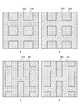
- FIG. 10A is a diagram showing an example of a pad 200 in which a square metal region 210 is arranged in an island shape in a bulging region 220. This is an example in which the proportion of the bulging region 220 is improved from that of the metal region 210. The amount of bulging of the metal region 210 to the bulging region 220 can be increased, and damage to the interlayer insulating film can be further reduced.
- B in FIG. 10 is an example in which the metal region 210 and the bulging region 220 are arranged interchangeably in the configuration of A in FIG. 10, and the square bulging region 220 is arranged in an island shape in the metal region 210. It is a figure which showed the example of the pad 200 which was configured.
- the proportion of the metal region 210 is relatively higher than that of the bulging region 220, and the connection resistance with the bonding wire can be reduced.
- C in FIG. 10 is a diagram showing an example in which the rectangular metal region 210 is arranged in the bulging region 220.
- D in FIG. 10 is a diagram showing an example in the case where the rectangular bulging region 220 is arranged in the metal region 210.
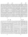
- FIG. 11A is a diagram showing an example of a case where the square-shaped metal region 210 is arranged in the bulging region 220. Further, FIG. 11B is a diagram showing an example in which the square-shaped bulging region 220 is arranged in the metal region 210.
- FIG. 11C is a diagram showing an example in which a metal region 210 is arranged in the central portion, and bulging regions 220 and metal regions 210 having a shape surrounding the metal region 210 in the central portion are alternately arranged. ..
- the metal region 210 and the bulging region 220 of C in FIG. 11 can also be configured in a concentric shape.
- FIG. 11D is a diagram showing an example in which a cross-shaped metal region 210 is arranged in the central portion, and bulging regions 220 and metal regions 210 adjacent to the metal region 210 in the central portion are alternately arranged. is there.
- the metal region 210 and the bulging region 220 can be formed in any shape.
- a pad 200 composed of a pad layer 201 including a metal region 210 and a bulging region 220 is arranged. Even when an impact is applied to the pad 200 by wire bonding or the like, the deformed metal region 210 bulges into the bulging region 220, so that the stress on the lower interlayer insulating film 135 or the like is relaxed, and the layers are laminated. Damage to the insulating film 135 and the like can be reduced.
- a normal wiring region can be arranged in the lower layer of such a pad 200, and the configuration of the semiconductor device 100 can be simplified.
- the pad 200 of the semiconductor device 100 of the first embodiment described above was composed of a single pad layer 201.
- the semiconductor device 100 of the second embodiment of the present disclosure is different from the above-described first embodiment in that a pad 200 composed of two or more pad layers is used.
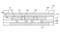
- FIG. 12 is a cross-sectional view showing a configuration example of the pad according to the second embodiment of the present disclosure. Similar to FIG. 3, FIG. 3 is a cross-sectional view showing a configuration example of a pad 200 portion of the semiconductor device 100. It differs from the pad 200 described in FIG. 3 in that the pad layer 202 is further arranged on the pad 200.
- the pad layer 202 in the figure is composed of a metal region 230 and a bulging region 240, similarly to the pad layer 201. Further, the pad layer 202 is arranged below the pad layer 201.
- the metal region 230 is a region composed of a metal such as Cu, like the metal region 210.
- the bulge region 240 is a region in which the cavity 241 is arranged and is arranged adjacent to the same layer of the metal region 230, similarly to the bulge region 220. In the bulging region 240, the deformed metal region 230 bulges during wire bonding or the like.
- the bulging region 240 can be arranged at a position that does not overlap with the bulging region 220.
- the strength of the pad 200 can be improved by laminating the pad layers 201 and 202, which are the mixed pad layers. Further, when the metal regions 210 and 230 bulge, they can be bulged to the bulging regions 240 and 230 adjacent to each other in the thickness direction, respectively. As a result, the stress on the underlying interlayer insulating film 135 and the like can be further relaxed.
- the metal regions 210 and 230 arranged in the pad layers 201 and 202, respectively, can be composed of metals having different Young's modulus.
- the metal region 210 may be made of Cu
- the metal region 230 may be made of a metal having a Young's modulus higher than that of Cu.
- Metals with a high Young's modulus include, for example, platinum (Pt), renium (Re), W, tantalum (Ta), iridium (Ir), rhodium (Rh), ruthenium (Ru), molybdenum (Mo), nickel (Ni).
- FIG. 13 is a diagram showing a configuration example of a pad according to the second embodiment of the present disclosure.
- FIG. 2 is a plan view showing a configuration example of the pad 200, as in FIG. 2.
- the dotted rectangle in the figure represents the metal region 230 and the bulging region 240 arranged in the inner layer.
- FIG. A in the figure is a diagram showing a configuration example of the pad 200 described in FIG. As shown by A in the figure, the metal region 230 and the bulging region 240 are arranged in a stripe shape in the same direction as the metal region 210 and the bulging region 220.
- B in the figure shows an example in which the striped metal region 230 and the bulging region 240 are arranged in directions 90 degrees different from the metal region 210 and the bulging region 220, unlike A in the figure. Is.
- the configuration of the pad 200 is not limited to this example.
- a composite pad layer composed of a metal region and a bulging region may be laminated in three or more layers.
- the pad 200 of the second embodiment of the present disclosure can improve the strength of the pad 200 by laminating the pad layers 201 and 202 in which the metal region and the bulging region are arranged. it can. Further, when the metal regions 210 and 230 bulge, they can bulge into the bulging regions 240 and 230 adjacent to each other in the thickness direction, respectively, and the stress on the interlayer insulating film 135 and the like can be further relaxed.
- the semiconductor device 100 of the second embodiment described above is configured by laminating a plurality of mixed pad layers composed of a metal region and a bulging region.
- the semiconductor device 100 of the third embodiment of the present disclosure is different from the above-described second embodiment in that it includes a pad layer composed of only a metal region.
- FIG. 14 is a diagram showing a configuration example of a pad according to a third embodiment of the present disclosure.
- FIG. 12 is a cross-sectional view showing a configuration example of a portion of the pad 200 of the semiconductor device 100, similarly to FIG. It differs from the pad 200 described in FIG. 12 in that the pad layer 203 is arranged instead of the pad layer 202.
- A represents the cross-sectional structure of the pad 200
- B in the figure represents the plan structure of the pad 200.
- the pad layer 203 is a pad layer composed of a metal region 250 and in which a bulging region is not arranged. Since the bulging region is not arranged, it has higher strength than the pad layer 201. By arranging the pad layer 203, the strength of the pad 200 can be improved.
- FIG. 15 is a cross-sectional view showing another configuration example of the pad according to the third embodiment of the present disclosure.
- the pad 200 in the figure is composed of a pad layer 204 and a pad layer 202 composed of a metal region 260. Even in this case, the strength of the pad 200 can be improved by arranging the pad layer 204. Further, since the pad layer 204 having only the metal region 260 is arranged on the surface of the pad 200, the contact area with the bonding wire can be widened, and the connection resistance can be reduced.
- the configuration of the pad 200 is not limited to this example.
- the pad 200 can be composed of three or more pad layers.
- at least one pad layer can be a hybrid pad layer in which the bulging region is arranged.
- the pad 200 may be formed by laminating pad layers made of metals having different Young's modulus.
- the pad layers 203 and 204 in which the bulging region is not arranged are arranged on the pad 200, and the strength of the pad 200 can be improved.
- the semiconductor device 100 of the first embodiment described above uses a bulging region 220 or the like made of an insulating material having a cavity 221.
- the semiconductor device 100 of the fourth embodiment of the present disclosure is different from the above-described first embodiment in that it includes a bulging region formed by voids.
- FIG. 16 is a cross-sectional view showing a configuration example of a pad according to a fourth embodiment of the present disclosure.
- FIG. 3 is a cross-sectional view showing a configuration example of a portion of the pad 200 of the semiconductor device 100, similarly to FIG. It differs from the pad 200 described in FIG. 3 in that the pad layer 205 is arranged instead of the pad layer 201.
- the pad layer 205 is a pad layer composed of a metal region 210 and a bulging region 270.
- the bulging region 270 is composed of voids.
- the metal region 210 is deformed by wire bonding, the deformed portion bulges into the bulging region 270 which is a gap.
- more metal regions 210 can be bulged because no insulation is present. Damage to the lower interlayer insulating film 135 and the like can be further reduced.
- the pad layer 205 can be formed by omitting the step H in FIG.
- the step of arranging the insulating material in the bulging region 270 can be omitted, and the manufacturing process of the pad 200 can be simplified.
- the configuration of the pad 200 is not limited to this example.
- the pad 200 can be composed of two or more pad layers.
- the pad layer 205 is arranged on the surface layer of the pad 200.
- the pad layer 202 of FIG. 3 can be arranged under the pad layer 205.
- more metal regions 210 are bulged by arranging the bulging regions 270 formed by voids in the pads 200. Can be done. It is possible to further reduce damage to the lower interlayer insulating film 135 and the like. In addition, the manufacturing process of the pad 200 can be simplified.
- the technology according to the present disclosure can be applied to various products.
- the present technology may be realized as a pad such as an image sensor.
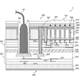
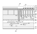
- FIG. 17 is a cross-sectional view showing a configuration example of an image sensor to which the present technology can be applied.
- FIG. 6 is a cross-sectional view showing a configuration example of the image sensor 1.
- the image sensor 1 in the figure is an example of the semiconductor device 100 described in FIG. 1, and represents an example of a semiconductor device connected to an external circuit by a bonding wire 20.
- the image sensor 1 is configured by bonding an image sensor chip 500 and a logic circuit chip 600.
- the image sensor chip 500 is a semiconductor chip in which a plurality of pixels 501 are arranged.
- the pixel 501 includes a photoelectric conversion unit, and converts light from a subject into an image signal.
- the logic circuit chip 600 is a semiconductor chip that generates a control signal for the pixel 501 of the image sensor chip 500 and processes the image signal generated by the pixel 501.
- the image sensor chip 500 in the figure includes a semiconductor substrate 520, a wiring region 530, protective films 522, 524, and 526, a color filter 551, a light-shielding film 552, a flattening film 553, and an on-chip lens 554. Be prepared.
- the semiconductor substrate 520 is a semiconductor substrate on which the semiconductor element portion of the pixel 501 is arranged.
- the semiconductor substrate 520 can be made of, for example, silicon (Si).
- a semiconductor element such as a photoelectric conversion unit is formed in a well region formed on a semiconductor substrate 520.
- the photoelectric conversion unit is described as an example of a semiconductor element.
- This photoelectric conversion unit is composed of an n-type semiconductor region 521.
- the photoelectric conversion unit is composed of a pn junction formed between the p-type well region around the n-type semiconductor region 521 and the n-type semiconductor region 521 in the figure.
- This pn junction constitutes a photodiode and performs photoelectric conversion when irradiated with incident light.
- the n-type semiconductor region 521 is arranged for each pixel 501.
- the semiconductor substrate 520 can be configured to have a thickness of, for example, several ⁇ m to several tens of ⁇ m.
- the protective film 522 is a film that is arranged on the surface of the semiconductor substrate 520 to protect the semiconductor substrate 520.
- the protective film 522 can be made of, for example, SiO 2 .
- the protective film 524 is a film that is arranged on the back surface of the semiconductor substrate 520 to protect the semiconductor substrate 520.
- the protective film 524 can be made of an inorganic material such as SiO 2 or silicon nitride SiN that transmits incident light.
- a separation region 525 is arranged between the pixels 501. The separation region 525 separates adjacent pixels 501 from each other.
- the separation region 525 is arranged in a trench formed from the back surface side of the semiconductor substrate 520, can be made of the same material as the protective film 524, and can be formed at the same time as the protective film 524.
- the protective film 526 is arranged adjacent to the protective film 524 on the back surface of the semiconductor substrate 520 and is a film that protects the semiconductor substrate 520. Further, the protective film 526 further flattens the back surface of the semiconductor substrate 520 on which the color filter 551 described later is formed.
- the protective film 526 for example, a film made of an organic material or an inorganic material that transmits incident light can be used.
- the wiring area 530 is an area in which wiring for transmitting a signal or the like of the pixel 501 is formed.
- the wiring region 530 is arranged on the surface side of the semiconductor substrate 520. Specifically, it is arranged adjacent to the protective film 522.
- the wiring region 530 is configured by laminating a wiring layer on which the wiring 531 is formed and an insulating layer 532 that insulates the wiring 531.
- the figure shows an example of a wiring region laminated in four layers. Wiring 531 arranged in different layers is connected by a via plug 533.
- the wiring 531 can be made of, for example, a metal such as copper (Cu) or tungsten (W).
- the insulating layer 532 can be made of, for example, SiO 2 .
- a protective film 536 is arranged on the outermost layer of the wiring region 530.
- the protective film 536 can be made of, for example, SiN.
- the color filter 551 is an optical filter that transmits light of a predetermined wavelength among the incident light.
- the color filter 551 is arranged for each pixel 501.
- a color filter 551 that transmits any of red light, green light, and blue light can be used.
- the light-shielding film 552 is a film that blocks incident light.
- the light-shielding film 552 is arranged at the boundary of the pixel 501 and blocks the light transmitted through the color filter 551 of the adjacent pixel 501. As a result, color mixing can be prevented.
- the flattening film 553 is a film that flattens the back surface of the semiconductor substrate 520 on which the on-chip lens 554 described later is formed.
- the flattening film 553 can be made of the same material as the on-chip lens 554.
- the on-chip lens 554 is a lens that is arranged for each pixel 501 and collects incident light on a photoelectric conversion unit.
- the image sensor 1 in the figure corresponds to a back-illuminated image sensor in which incident light is emitted from the back surface, which is a surface different from the front surface on which the wiring region 530 of the semiconductor substrate 520 is arranged. ..
- the logic circuit chip 600 includes a semiconductor substrate 620, a protective film 653, and a wiring area 630.
- elements of a circuit that generates a control signal of the pixel 501 of the image sensor chip 500 and a circuit that processes an image signal are arranged.
- the protective film 653 is a film that is arranged on the back surface of the semiconductor substrate 620 and protects the semiconductor substrate 620.
- the wiring area 630 is composed of a wiring 631, a via plug 633, and an insulating layer 632, and a protective film 636 is arranged on the outermost layer.
- the protective film 636 and the protective film 536 of the image sensor chip 500 are bonded together.
- the protective film 636 can be made of SiN in the same manner as the protective film 536.
- the via plug 565 is a via plug formed through the semiconductor substrate 520 and the wiring region 530
- the via plug 566 is a via plug formed through the semiconductor substrate 520
- the wiring 567 is a wiring formed on the protective film 526 on the back surface side of the semiconductor substrate 520 to electrically connect the via plugs 565 and 566.
- the bottom of the via plug 565 is formed adjacent to the pad 635 of the logic circuit chip 600, and is electrically connected to the pad 635.
- the signal of the wiring area 530 of the logic circuit chip 600 is transmitted to the wiring area 630 of the logic circuit chip 600 by the paths of the via plug 566, the wiring 567, and the via plug 565.
- the pad 635 is connected to a pad 634 described later in the wiring area 630 of the logic circuit chip 600.
- a pad for wire bonding is arranged around the image sensor 1.
- the pad 634 is arranged on the logic circuit chip 600. Further, the image sensor chip 500 is formed with an opening 562 that reaches the pad 634. Wire bonding is performed on the pad 634 through the opening 562, and the bonding wire 20 is connected to the pad 634. At this time, the connecting portion 22 of the bonding wire 20 with the pad 634 is formed inside the opening 562.
- FIGS. 18 and 19 are diagrams showing an example of a method for manufacturing an image sensor to which the present technology can be applied.
- the figure shows an example of the manufacturing method of the pad 634 peripheral region for wire bonding among the manufacturing methods of the image sensor 1.
- the image sensor chip 500 and the logic circuit chip 600 in which the pad 634 is embedded in the wiring area 630 are bonded to each other to form the via plugs 565 and 566 and the wiring 567.
- the on-chip lens 554 is arranged on the image sensor chip 500 (FIG. 18).
- an opening 562 that reaches the pad 634 of the logic circuit chip 600 is formed from the image sensor chip 500 side. This can be done by dry etching (Fig. 19). Thereby, the pad 634 for wire bonding can be formed. Next, wire bonding is performed by the bonding wire 20, and the image sensor 1 can be connected to an external substrate or the like.
- the image sensor 1 to which the present disclosure can be applied has been described above.
- the present technology may be applied to the pad 634 among the configurations described above.
- the pad 200 described in FIG. 1 can be applied to the pad 634.
- damage to the wiring region 630 when wire bonding to the pad 634 can be reduced.
- the pad 634 for wire bonding may be arranged in the wiring region 530 of the image sensor chip 500 in the image sensor 1 configured in a laminated manner or on the surface on the surface side to which the incident light is irradiated. Further, it is also possible to adopt a configuration in which the pad 634 for wire bonding is arranged on the surface of the logic circuit chip 600 opposite to the surface laminated with the image sensor chip 500.
- drawings in the above-described embodiment are schematic, and the ratio of the dimensions of each part does not always match the actual one.
- the drawings include parts having different dimensional relationships and ratios from each other.
- a mixed pad layer which is a pad layer in which a metal region and a bulging region where the deformed portion bulges when the metal region is deformed are arranged in the same layer, is adjacent to an interlayer insulating film formed on a semiconductor substrate.
- the bulging region is composed of voids.
- the pad is formed by laminating a plurality of pad layers including at least one hybrid pad layer.
- the pad includes a pad layer composed of metal regions having different Young's modulus.
- the metal regions are arranged at a ratio of 0.5 or more in the mixed pad layer.
- Imaging element 20 Bonding wire 90 Inspection probe 100
- Semiconductor device 131-136 Interlayer insulation film 142 Via plug 151, 152 Wiring layer 200, 634 Pad 201-205 Pad layer 210, 230, 250, 260 Metal region 211 Protruding part 220, 240 270 bulging area 221 and 241 cavities 401 metal layer 402 openings
Landscapes
- Internal Circuitry In Semiconductor Integrated Circuit Devices (AREA)
- Wire Bonding (AREA)
- Solid State Image Pick-Up Elements (AREA)
Abstract
パッドを具備する半導体装置におけるパッドの構成を簡略化する。 半導体装置は、パッドを具備する。その半導体装置が具備するパッドは、混成パッド層が半導体基板に形成された層間絶縁膜に隣接して配置されて構成される。そのパッドを構成するその混成パッド層は、金属領域と膨出領域とが同層に配置されるパッド層である。その混成パッド層に配置されるその膨出領域は、その金属領域が変形した際の変形部分が膨出する領域である。
Description
本開示は、半導体装置および半導体装置の製造方法に関する。詳しくは、半導体チップの表面にパッドが配置される半導体装置および当該半導体装置の製造方法に関する。
従来、半導体チップの表面にパッドが配置されて構成された半導体装置が使用されている。このパッドは、信号を半導体チップの外部に取り出すための電極である。ワイヤボンディングによりパッドにボンディングワイヤが接続され、このボンディングワイヤを介して信号の伝達が行われる。ワイヤボンディングでは、金(Au)線等をボンディングワイヤとして使用し、パッドに溶着させることにより電気的な接続を得ることができる。このボンディングワイヤの溶着は、先端が球形状に加工されたボンディングワイヤをパッドに加熱圧接することにより行うことができる。しかし、このワイヤボンディングの際に半導体チップが破損する場合がある。例えば、ワイヤボンディングの衝撃により、パッドの直下の層間絶縁膜等が損傷を受け、き裂を生じる場合がある。
このような、ワイヤボンディングの際の半導体チップの損傷を防ぐため、パッドの直下の絶縁層に高硬度の構造物であるタングステン構造物を配置する半導体装置が提案されている(例えば、特許文献1参照。)。このタングステン構造物は、一定長、一定幅の板が複数枚一定間隔で並置された構造を有する。
上述の従来技術では、パッドの直下の絶縁層にタングステン構造物を配置する必要があり、構成が複雑になるという問題がある。
本開示は、上述した問題点に鑑みてなされたものであり、半導体装置のパッドの構成を簡略化することを目的としている。
本開示は、上述の問題点を解消するためになされたものであり、その第1の態様は、金属領域と当該金属領域が変形した際の変形部分が膨出する膨出領域とが同層に配置されるパッド層である混成パッド層が半導体基板に形成された層間絶縁膜に隣接して配置されて構成されるパッドを具備する半導体装置である。
また、この第1の態様において、上記膨出領域は、内部に空洞を有する部材により構成されてもよい。
また、この第1の態様において、上記膨出領域は、金属膜に形成された開口部の頂部を閉塞することにより内部に上記空洞を形成した上記部材により構成されてもよい。
また、この第1の態様において、上記金属膜の開口部は、断面が逆テーパ形状に構成されてもよい。
また、この第1の態様において、上記金属膜の開口部は、断面の幅の1.5倍以上の高さに構成されてもよい。
また、この第1の態様において、上記膨出領域は、空隙により構成されてもよい。
また、この第1の態様において、上記パッドは、少なくとも1つの上記混成パッド層を含む複数のパッド層が積層されて構成されてもよい。
また、この第1の態様において、上記パッドは、異なるヤング率の金属領域により構成されるパッド層を備えてもよい。
また、この第1の態様において、上記混成パッド層において上記金属領域は0.5以上の割合に配置されてもよい。
また、この第1の態様において、上記混成パッド層の金属領域は、ビアプラグにより配線層と接続されてもよい。
また、この第1の態様において、上記パッドは、ワイヤボンディングのためのパッドであってもよい。
また、この第1の態様において、上記パッドは、検査プローブが当接されるパッドであってもよい。
また、本開示の第2の態様は、金属領域と当該金属領域が変形した際の変形部分が膨出する膨出領域とが同層に配置されるパッド層である混成パッド層の上記金属領域を半導体基板に形成された層間絶縁膜に隣接して配置する金属領域配置工程と、
上記膨出領域を上記形成された金属領域と同層に配置する膨出領域配置工程と
を具備する半導体装置の製造方法である。
上記膨出領域を上記形成された金属領域と同層に配置する膨出領域配置工程と
を具備する半導体装置の製造方法である。
このような態様を採ることにより、パッドを構成するパッド層の金属領域が隣接する膨出領域に膨出することとなり、金属領域がパッド層に平行な方向に変形するという作用をもたらす。パッド層に垂直な方向への金属領域の変形の抑制が想定される。
次に、図面を参照して、本開示を実施するための形態(以下、実施の形態と称する)を説明する。以下の図面において、同一または類似の部分には同一または類似の符号を付している。また、以下の順序で実施の形態の説明を行う。
1.第1の実施の形態
2.第2の実施の形態
3.第3の実施の形態
4.第4の実施の形態
5.撮像素子への応用例
1.第1の実施の形態
2.第2の実施の形態
3.第3の実施の形態
4.第4の実施の形態
5.撮像素子への応用例
<1.第1の実施の形態>
[半導体装置の構成]
図1は、本開示の実施の形態に係る半導体装置の構成例を示す図である。同図は、半導体チップ形状の半導体装置100が基板10に実装される様子を表した図である。同図の半導体装置100は、端部の表面に複数のパッド200が配置される。このパッド200は、半導体装置100の外部の装置との間において信号のやり取りを行う際に、信号の伝達を行う電極である。一方、基板10にもパッド11が配置される。半導体装置100が基板10にダイボンディングされた後、ボンディングワイヤ20により、半導体装置100のパッド200と基板10のパッド11とが1対1に接続される。
[半導体装置の構成]
図1は、本開示の実施の形態に係る半導体装置の構成例を示す図である。同図は、半導体チップ形状の半導体装置100が基板10に実装される様子を表した図である。同図の半導体装置100は、端部の表面に複数のパッド200が配置される。このパッド200は、半導体装置100の外部の装置との間において信号のやり取りを行う際に、信号の伝達を行う電極である。一方、基板10にもパッド11が配置される。半導体装置100が基板10にダイボンディングされた後、ボンディングワイヤ20により、半導体装置100のパッド200と基板10のパッド11とが1対1に接続される。
[パッドの平面構成]
図2は、本開示の第1の実施の形態に係るパッドの構成例を示す図である。同図は、パッド200の構成例を表す平面図である。同図のパッド200は、金属領域210および膨出領域220がストライプ状に配置されて構成される。金属領域210は、信号を伝達する導体である。この金属領域210は、銅(Cu)等の金属により構成され、後述する配線に接続される。この金属領域210にボンディングワイヤが接続されて電気信号が伝達される。
図2は、本開示の第1の実施の形態に係るパッドの構成例を示す図である。同図は、パッド200の構成例を表す平面図である。同図のパッド200は、金属領域210および膨出領域220がストライプ状に配置されて構成される。金属領域210は、信号を伝達する導体である。この金属領域210は、銅(Cu)等の金属により構成され、後述する配線に接続される。この金属領域210にボンディングワイヤが接続されて電気信号が伝達される。
膨出領域220は、金属領域210に隣接して配置され、金属領域210が変形した際の変形部分が膨出する領域である。同図の膨出領域220は、例えば、内部に空洞を有する絶縁物により構成することができる。金属領域210は、ワイヤボンディングの際、圧縮されて変形する。これにより、金属領域210を構成する金属の一部が膨出する。すなわち、変形前の金属領域210の領域から一部の金属がはみ出す。膨出領域220は、このはみ出す部分である変形した金属領域210を膨出させる領域である。この膨出領域220を配置することにより、金属領域210の下層への膨出を防ぐことができる。金属領域210の膨出の詳細については、後述する。
[パッドの断面構成]
図3は、本開示の第1の実施の形態に係るパッドの構成例を示す断面図である。同図は、半導体装置100のうちのパッド200の部分の構成例を表す断面図である。半導体装置100は、半導体基板121と、絶縁膜122と、層間絶縁膜131乃至136と、配線層151および152と、コンタクトプラグ141と、ビアプラグ142および143と、保護膜161と、パッド200とを備える。
図3は、本開示の第1の実施の形態に係るパッドの構成例を示す断面図である。同図は、半導体装置100のうちのパッド200の部分の構成例を表す断面図である。半導体装置100は、半導体基板121と、絶縁膜122と、層間絶縁膜131乃至136と、配線層151および152と、コンタクトプラグ141と、ビアプラグ142および143と、保護膜161と、パッド200とを備える。
半導体基板121は、半導体装置100に配置される素子の半導体部分(拡散領域)が形成される半導体の基板である。この半導体基板121には、例えば、シリコン(Si)により構成された基板を使用することができる。半導体基板121にp型およびn型の半導体領域を形成することにより、素子の拡散領域が形成される。
絶縁膜122は、半導体基板121の表面を絶縁するものである。この絶縁膜122は、酸化シリコン(SiO2)や窒化シリコン(SiN)により構成され、半導体基板121の表面を絶縁するとともに保護する。
配線層151および152は、半導体基板121の拡散層やパッド200に信号を伝達する配線である。この配線層151および152は、例えば、Cu等の金属により構成することができる。また、配線層151および152は、それぞれ異なる層に配置される。層間絶縁膜131乃至136は、配線層151および152等を絶縁するものである。これら配線層151および152ならびに層間絶縁膜131乃至136は、配線領域を構成する。同図は、2層構成の配線領域の例を表したものである。
コンタクトプラグ141は、半導体基板121の拡散層および配線層151を接続するものである。また、ビアプラグ142は、配線層151および152を接続するものである。ビアプラグ143は、配線層152およびパッド200の金属領域210を接続するものである。これら、コンタクトプラグ141ならびにビアプラグ142および143は、柱状の金属により構成され、異なる層に配置された配線層等を接続することができる。コンタクトプラグ141ならびにビアプラグ142および143は、例えば、タングステン(W)やCuにより構成することができる。
パッド200は、上述のように、金属領域210および膨出領域220により構成される。同図の金属領域210および膨出領域220は、同層に配置され、パッド層201を構成する。同図のパッド200は、1つのパッド層201により構成される例を表したものである。図12において後述するように、積層された複数のパッド層により、パッド200を構成することもできる。なお、膨出領域220が配置されたパッド層を混成パッド層と称する。また、パッド層201は、層間絶縁膜135に隣接して配置される。
金属領域210は、上述のコンタクトプラグ141、ビアプラグ142および143ならびに配線層151および152を介して半導体基板121に接続される。なお、パッド200において、金属領域210は、0.5以上の割合に配置すると好適である。すなわち、複数の金属領域210の合計面積を複数の膨出領域220の合計面積以上に構成すると、金属の領域が増加し、パッド200の強度を向上させることができるためである。
膨出領域220は、金属領域210と同層に隣接して配置される。膨出領域220は、例えば、SiO2等の絶縁物により構成することができる。また、同図の膨出領域220は、内部に空洞221が配置される。この空洞221により、膨出領域220は、層間絶縁膜135より低い強度に構成される。これにより、上述の金属領域210が変形する際、金属領域210は膨出領域220に膨出し、金属領域210の層間絶縁膜135への膨出を抑制することができる。このように、膨出領域220は、空洞221を有する部材により構成することができる。
保護膜161は、半導体装置100の表面を保護するものである。この保護膜161は、例えば、SiNにより構成することができる。
[ワイヤボンディング]
図4は、従来の半導体装置の例を表す断面図である。同図は、従来の半導体装置300においてワイヤボンディング等を行った場合を比較例として表した図である。同図の半導体装置300は、パッド200の代わりにパッド310を備える点で、図3において説明した半導体装置100と異なる。パッド310は、単一の金属により構成されるパッドである。
図4は、従来の半導体装置の例を表す断面図である。同図は、従来の半導体装置300においてワイヤボンディング等を行った場合を比較例として表した図である。同図の半導体装置300は、パッド200の代わりにパッド310を備える点で、図3において説明した半導体装置100と異なる。パッド310は、単一の金属により構成されるパッドである。
同図におけるAは、パッド310にワイヤボンディングを行った場合の例を表した図である。このワイヤボンディングは、例えば、次の手順により行うことができる。キャピラリーと称される器具にボンディングワイヤ20を通し、放電加熱によりボンディングワイヤ20の先端部を球状にする。次に、キャピラリーを使用してボンディングワイヤ20の先端部をパッド310に加熱圧接する。これにより、ボンディングワイヤ20およびパッド310の金属が接合される。この際の圧接により、パッド310が加圧されて変形する。変形したパッド310が半導体装置100の厚み方向に膨出するため、下層の層間絶縁膜や配線層が損傷を受ける。例えば、き裂301を生じる。
同図におけるBは、半導体装置100を検査する工程において、検査プローブ90がパッド310に当接される場合の例を表した図である。半導体装置100の検査は、検査プローブ90をパッド310に当接し、電気信号の印加および測定を行うことにより実行される。検査プローブ90およびパッド310の接触抵抗を低減するため、検査プローブ90は比較的高い圧力においてパッド310に当接される。このため、パッド310が変形して層間絶縁膜等が損傷し、き裂302を生じる。このようなき裂301および302の発生により半導体装置100が破損する。
[膨出領域の効果]
図5は、本開示の第1の実施の形態に係るワイヤボンディングの一例を示す図である。同図は、図4におけるAと同様に、半導体装置100にワイヤボンディングを行った場合の例を表した図である。同図の破線は、ワイヤボンディング前の膨出領域220を表す。パッド200では、ワイヤボンディングにより金属領域210が変形する際、変形した金属領域210は、膨出領域220の側に膨出する。同層に隣接する膨出領域220が内部に空洞221を有する脆弱な形状に構成されるためである。同図の膨出部211は、この膨出した金属領域210を表す。この膨出部211により膨出領域220は潰れた形状となる。一方、下層の層間絶縁膜135は、殆ど変形せず、き裂等の発生を防止することができる。膨出領域220と比較して層間絶縁膜135は緻密な膜質に構成されるためである。
図5は、本開示の第1の実施の形態に係るワイヤボンディングの一例を示す図である。同図は、図4におけるAと同様に、半導体装置100にワイヤボンディングを行った場合の例を表した図である。同図の破線は、ワイヤボンディング前の膨出領域220を表す。パッド200では、ワイヤボンディングにより金属領域210が変形する際、変形した金属領域210は、膨出領域220の側に膨出する。同層に隣接する膨出領域220が内部に空洞221を有する脆弱な形状に構成されるためである。同図の膨出部211は、この膨出した金属領域210を表す。この膨出部211により膨出領域220は潰れた形状となる。一方、下層の層間絶縁膜135は、殆ど変形せず、き裂等の発生を防止することができる。膨出領域220と比較して層間絶縁膜135は緻密な膜質に構成されるためである。
このように、金属領域210に隣接して膨出領域220を配置することにより、金属領域210がパッド200の表面に平行な方向に膨れて変形し、ワイヤボンディングの衝撃が吸収される。パッド200の下層への応力が緩和され、層間絶縁膜135や配線層151および152の損傷を軽減することができる。半導体装置100の表面にパッド層201を配置することにより、内層の損傷を防止可能なパッド200を構成することができる。パッド200を検査プローブが当接されるパッドとして使用する場合にも同様の効果を得ることができる。パッド200の下層には、層間絶縁膜135等や配線層152等による通常の配線領域を配置することができ、半導体装置100の構成を簡略化することができる。
なお、膨出領域220の構成は、この例に限定されない。例えば、空洞を有する導電性の材料により構成することもできる。例えば、空洞を有する金属により構成された膨出領域220を使用することもできる。この場合には、金属領域210より低い硬度の金属により膨出領域220を形成すると好適である。
[製造方法]
図6乃至8は、本開示の第1の実施の形態に係る半導体装置の製造方法の一例を示す図である。まず、半導体基板121に絶縁膜122を形成する。これは、例えば、半導体基板121を熱酸化することにより行うことができる。次に、層間絶縁膜131を積層する。これは、例えば、CVD(Chemical Vapor Deposition)により行うことができる(図6におけるA)。次に、コンタクトプラグ141を配置する位置の層間絶縁膜131および絶縁膜122に開口部を形成する。これは、例えば、ドライエッチングにより行うことができる。次に、W等の金属層を成膜して開口部に金属を埋め込む。これは、例えば、CVDにより行うことができる。次に、化学的機械的研磨(CMP:Chemical Mechanical Polishing)等により表面の金属を研削して除去する。これにより、コンタクトプラグ141を形成する(図6におけるB)。
図6乃至8は、本開示の第1の実施の形態に係る半導体装置の製造方法の一例を示す図である。まず、半導体基板121に絶縁膜122を形成する。これは、例えば、半導体基板121を熱酸化することにより行うことができる。次に、層間絶縁膜131を積層する。これは、例えば、CVD(Chemical Vapor Deposition)により行うことができる(図6におけるA)。次に、コンタクトプラグ141を配置する位置の層間絶縁膜131および絶縁膜122に開口部を形成する。これは、例えば、ドライエッチングにより行うことができる。次に、W等の金属層を成膜して開口部に金属を埋め込む。これは、例えば、CVDにより行うことができる。次に、化学的機械的研磨(CMP:Chemical Mechanical Polishing)等により表面の金属を研削して除去する。これにより、コンタクトプラグ141を形成する(図6におけるB)。
次に、層間絶縁膜132を配置し、配線層151を形成する領域をエッチングすることにより開口部を形成する。なお、層間絶縁膜131および132の間には、SiN等によるハードマスク層(不図示)が配置される。次に、この層間絶縁膜132の開口部にCu等の金属を埋め込んで配線層151を形成する。これは、ダマシン法により形成することができる。具体的には、次の手順により形成することができる。まず、開口部を含む半導体基板121の表面にバリア層およびめっきのシード層を積層する。バリア層は、配線層151等の金属の拡散を防ぐものであり、窒化チタン(TiN)等により構成することができる。シード層は、Cuにより構成することができる。次に、Cuの膜をめっきにより成膜し、開口部にCuを埋め込む。次に、CMPにより開口部以外のCu等を研削して除去する。これにより、配線層151を配置することができる(図6におけるC)。
次に、層間絶縁膜133および134を成膜する。層間絶縁膜134に配線層152を配置するための開口部を形成し、層間絶縁膜133にビアプラグ142を配置するための開口部を形成する。その後、ダマシン法によりビアプラグ142および配線層152を同時に形成する(図6のおけるD)。なお、配線層を3層以上に多層化する場合には、この層間絶縁膜133および134、ビアプラグ142ならびに配線層152の形成と同様の工程を繰り返すことにより行うことができる。次に、層間絶縁膜135を成膜し、ダマシン法によりビアプラグ143を配置する(図6におけるE)。
次に、層間絶縁膜136を成膜し、パッド200を配置する位置に開口部を形成して金属層401を埋め込む(図7におけるF)。次に、膨出領域220を配置する位置に開口部を有するレジストを金属層401の表面に配置する。次に、このレジストをマスクとして金属層401をエッチングする。これは、例えば、ドライエッチングにより行うことができる。これにより、金属領域210を配置するとともに開口部402を形成することができる(図7におけるG)。当該工程は、請求の範囲に記載の金属領域配置工程の一例である。
次に膨出領域220の材料となる絶縁物膜403を成膜する。これは、例えば、PVD(Physical Vapor Deposition)により行うことができる。開口部402の底部よりも側面の方に多くの絶縁物膜403が析出する成膜法を採用することにより、開口部402に絶縁物を埋め込むと同時に空洞221を形成することができる(図7におけるH)。次に、金属領域210の表面の絶縁物膜403をCMPにより研削して除去する。これにより、膨出領域220を金属領域210と同層に隣接して配置することができる(図8におけるI)。当該工程は、請求の範囲に記載の膨出領域配置工程の一例である。
次に、保護膜161の材料となる絶縁物膜405を成膜する(図8におけるJ)。次に、絶縁物膜405におけるパッド200を配置する位置に開口部406を形成する(図8におけるK)。これにより、保護膜161およびパッド200を形成することができる。
[他の製造方法]
図9は、本開示の第1の実施の形態に係る半導体装置の製造方法の他の例を示す図である。同図は、図7におけるGにおいて説明した金属領域210の材料となる金属層401のエッチングの他の例を表した図である。
図9は、本開示の第1の実施の形態に係る半導体装置の製造方法の他の例を示す図である。同図は、図7におけるGにおいて説明した金属領域210の材料となる金属層401のエッチングの他の例を表した図である。
同図におけるAは、断面が逆テーパ形状の開口部402を形成する場合の例である。開口部402の表面の幅を底部の幅より狭くすることにより、絶縁物膜403を積層する際の開口部402の閉塞を容易に行うことができる。比較的大きな空洞221を配置することが可能となる。
同図におけるBは、開口部402のアスペクト比を調整する場合の例である。同図におけるBの開口部402の幅Wに対して高さ(深さ)Hが大きい場合、スパッタリング等のPVDにより形成された絶縁物の粒子の開口部402の底部への到達が軽減される。これにより、開口部402の表面近傍の側面に多くの絶縁物粒子が堆積し、大きな空洞221を有する膨出領域220を形成することができる。開口部402の高さHを幅Wの1.5倍以上の大きさにすることにより、開口部402の閉塞を容易に行うことができる。
[パッドの他の構成]
図10および11は、本開示の第1の実施の形態に係るパッドの構成の他の例を示す図である。図10におけるAは、正方形の金属領域210が膨出領域220の中に島状に配置されて構成されたパッド200の例を表した図である。金属領域210より膨出領域220の割合を向上させた例である。金属領域210の膨出領域220への膨出量を増加させることができ、層間絶縁膜の損傷をより低減することができる。
図10および11は、本開示の第1の実施の形態に係るパッドの構成の他の例を示す図である。図10におけるAは、正方形の金属領域210が膨出領域220の中に島状に配置されて構成されたパッド200の例を表した図である。金属領域210より膨出領域220の割合を向上させた例である。金属領域210の膨出領域220への膨出量を増加させることができ、層間絶縁膜の損傷をより低減することができる。
図10におけるBは、図10におけるAの構成において金属領域210および膨出領域220を入れ替えて配置した場合の例であり、正方形の膨出領域220が金属領域210の中に島状に配置されて構成されたパッド200の例を表した図である。膨出領域220より金属領域210の割合が比較的高く、ボンディングワイヤとの接続抵抗を低減させることができる。
図10におけるCは、長方形の金属領域210を膨出領域220の中に配置する場合の例を表した図である。また、図10におけるDは、長方形の膨出領域220を金属領域210の中に配置する場合の例表した図である。
図11におけるAは、ロの字形状の金属領域210を膨出領域220の中に配置した場合の例表した図である。また、図11におけるBは、ロの字形状の膨出領域220を金属領域210の中に配置する場合の例を表した図である。
図11におけるCは、中央部に金属領域210を配置し、この中央部の金属領域210を囲繞する形状の膨出領域220および金属領域210を交互に配置する場合の例を表した図である。なお、図11におけるCの金属領域210および膨出領域220は、同心円形状に構成することもできる。
図11におけるDは、中央部に十字形状の金属領域210を配置し、この中央部の金属領域210に隣接する膨出領域220および金属領域210を交互に配置する場合の例を表した図である。以上説明したように、金属領域210および膨出領域220は、任意の形状に構成することができる。
以上説明したように、本開示の第1の実施の形態の半導体装置100には、金属領域210および膨出領域220を備えるパッド層201により構成されたパッド200が配置される。ワイヤボンディング等によりパッド200に衝撃が加えられた場合であっても、変形した金属領域210が膨出領域220に膨出することにより、下層の層間絶縁膜135等への応力が緩和され、層間絶縁膜135等の損傷を軽減することができる。このようなパッド200の下層には通常の配線領域を配置することができ、半導体装置100の構成を簡略化することができる。
<2.第2の実施の形態>
上述の第1の実施の形態の半導体装置100のパッド200は、単一のパッド層201により構成されていた。これに対し、本開示の第2の実施の形態の半導体装置100は、2層以上のパッド層により構成されるパッド200を使用する点で、上述の第1の実施の形態と異なる。
上述の第1の実施の形態の半導体装置100のパッド200は、単一のパッド層201により構成されていた。これに対し、本開示の第2の実施の形態の半導体装置100は、2層以上のパッド層により構成されるパッド200を使用する点で、上述の第1の実施の形態と異なる。
[パッドの断面構成]
図12は、本開示の第2の実施の形態に係るパッドの構成例を示す断面図である。同図は、図3と同様に、半導体装置100のうちのパッド200部分の構成例を表す断面図である。パッド200にパッド層202がさらに配置される点で、図3において説明したパッド200と異なる。
図12は、本開示の第2の実施の形態に係るパッドの構成例を示す断面図である。同図は、図3と同様に、半導体装置100のうちのパッド200部分の構成例を表す断面図である。パッド200にパッド層202がさらに配置される点で、図3において説明したパッド200と異なる。
同図のパッド層202は、パッド層201と同様に、金属領域230および膨出領域240により構成される。また、パッド層202は、パッド層201の下層に配置される。
金属領域230は、金属領域210と同様に、Cu等の金属により構成される領域である。膨出領域240は、膨出領域220と同様に、金属領域230の同層に隣接して配置され、空洞241が配置される領域である。膨出領域240には、ワイヤボンディング等の際に、変形した金属領域230が膨出する。なお、膨出領域240は、膨出領域220とは重ならない位置に配置することができる。
混成パッド層であるパッド層201および202を積層することにより、パッド200の強度を向上させることができる。また、金属領域210および230が膨出する際、厚さ方向に隣接する膨出領域240および230にそれぞれ膨出させることもできる。これにより、下層の層間絶縁膜135等への応力をさらに緩和することができる。
また、パッド層201および202にそれぞれ配置される金属領域210および230をヤング率が異なる金属により構成することもできる。例えば、金属領域210をCuにより構成し、金属領域230をCuより高いヤング率の金属により構成することもできる。ヤング率が高い金属には、例えば、白金(Pt)、レニウム(Re)、W、タンタル(Ta)、イリジウム(Ir)、ロジウム(Rh)、ルテニウム(Ru)、モリブデン(Mo)、ニッケル(Ni)、コバルト(Co)、鉄(Fe)、マンガン(Mn)、クロム(Cr)、バナジウム(V)、チタン(Ti)およびベリリウム(Be)が該当する。ヤング率が低い金属により構成された金属領域を備えるパッド層に応力を集中させて膨出領域に金属領域を膨出させるとともに、ヤング率が高い金属により構成された金属領域を備えるパッド層によりパッド200の変形を軽減することができる。下層の層間絶縁膜135等への応力を軽減することができる。
[パッドの平面構成]
図13は、本開示の第2の実施の形態に係るパッドの構成例を示す図である。同図は、図2と同様に、パッド200の構成例を表す平面図である。同図の点線の矩形は、内層に配置された金属領域230および膨出領域240を表す。同図におけるAは、図12において説明したパッド200の構成例を表す図である。同図におけるAに表したように、金属領域230および膨出領域240は、金属領域210および膨出領域220と同じ方向のストライプ状に配置される。
図13は、本開示の第2の実施の形態に係るパッドの構成例を示す図である。同図は、図2と同様に、パッド200の構成例を表す平面図である。同図の点線の矩形は、内層に配置された金属領域230および膨出領域240を表す。同図におけるAは、図12において説明したパッド200の構成例を表す図である。同図におけるAに表したように、金属領域230および膨出領域240は、金属領域210および膨出領域220と同じ方向のストライプ状に配置される。
同図におけるBは、同図におけるAとは異なり、ストライプ状の金属領域230および膨出領域240を金属領域210および膨出領域220とは90度異なる方向に配置した場合の例を表した図である。
なお、パッド200の構成は、この例に限定されない。例えば、金属領域および膨出領域からなる混成パッド層を3層以上積層する構成にすることもできる。
これ以外の半導体装置100の構成は本開示の第1の実施の形態において説明した半導体装置100の構成と同様であるため、説明を省略する。
以上説明したように、本開示の第2の実施の形態のパッド200は、金属領域および膨出領域が配置されたパッド層201および202を積層することにより、パッド200の強度を向上させることができる。また、金属領域210および230が膨出する際、厚さ方向に隣接する膨出領域240および230にそれぞれ膨出させることができ、層間絶縁膜135等への応力をさらに緩和することができる。
<3.第3の実施の形態>
上述の第2の実施の形態の半導体装置100は、金属領域および膨出領域からなる混成パッド層が複数積層されて構成されていた。これに対し、本開示の第3の実施の形態の半導体装置100は、金属領域のみからなるパッド層を備える点で、上述の第2の実施の形態と異なる。
上述の第2の実施の形態の半導体装置100は、金属領域および膨出領域からなる混成パッド層が複数積層されて構成されていた。これに対し、本開示の第3の実施の形態の半導体装置100は、金属領域のみからなるパッド層を備える点で、上述の第2の実施の形態と異なる。
[パッドの構成]
図14は、本開示の第3の実施の形態に係るパッドの構成例を示す図である。同図は、図12と同様に、半導体装置100のうちのパッド200の部分の構成例を表す断面図である。パッド層202の代わりにパッド層203が配置される点で、図12において説明したパッド200と異なる。同図におけるAはパッド200の断面の構成を表し、同図におけるBはパッド200の平面の構成を表す。
図14は、本開示の第3の実施の形態に係るパッドの構成例を示す図である。同図は、図12と同様に、半導体装置100のうちのパッド200の部分の構成例を表す断面図である。パッド層202の代わりにパッド層203が配置される点で、図12において説明したパッド200と異なる。同図におけるAはパッド200の断面の構成を表し、同図におけるBはパッド200の平面の構成を表す。
パッド層203は、金属領域250により構成され、膨出領域が配置されないパッド層である。膨出領域が配置されないため、パッド層201より高い強度を有する。このパッド層203を配置することにより、パッド200の強度を向上させることができる。
[パッドの他の構成]
図15は、本開示の第3の実施の形態に係るパッドの他の構成例を示す断面図である。同図のパッド200は、金属領域260により構成されるパッド層204およびパッド層202により構成される。この場合においても、パッド層204を配置することにより、パッド200の強度を向上させることができる。また、金属領域260のみを有するパッド層204がパッド200の表面に配置されるため、ボンディングワイヤとの接触面積を広くすることができ、接続抵抗を低減することができる。
図15は、本開示の第3の実施の形態に係るパッドの他の構成例を示す断面図である。同図のパッド200は、金属領域260により構成されるパッド層204およびパッド層202により構成される。この場合においても、パッド層204を配置することにより、パッド200の強度を向上させることができる。また、金属領域260のみを有するパッド層204がパッド200の表面に配置されるため、ボンディングワイヤとの接触面積を広くすることができ、接続抵抗を低減することができる。
なお、パッド200の構成は、この例に限定されない。例えば、3層以上のパッド層によりパッド200を構成することもできる。この場合、少なくとも1つのパッド層は、膨出領域が配置された混成パッド層にすることができる。また、異なるヤング率の金属により構成されたパッド層が積層されたパッド200にすることもできる。
これ以外の半導体装置100の構成は本開示の第2の実施の形態において説明した半導体装置100の構成と同様であるため、説明を省略する。
以上説明したように、本開示の第3の実施の形態の半導体装置100は、パッド200に膨出領域が配置されないパッド層203および204が配置され、パッド200の強度を向上させることができる。
<4.第4の実施の形態>
上述の第1の実施の形態の半導体装置100は、空洞221を有する絶縁物により構成された膨出領域220等を使用していた。これに対し、本開示の第4の実施の形態の半導体装置100は、空隙により構成された膨出領域を備える点で、上述の第1の実施の形態と異なる。
上述の第1の実施の形態の半導体装置100は、空洞221を有する絶縁物により構成された膨出領域220等を使用していた。これに対し、本開示の第4の実施の形態の半導体装置100は、空隙により構成された膨出領域を備える点で、上述の第1の実施の形態と異なる。
[パッドの断面構成]
図16は、本開示の第4の実施の形態に係るパッドの構成例を示す断面図である。同図は、図3と同様に、半導体装置100のうちのパッド200の部分の構成例を表す断面図である。パッド層201の代わりにパッド層205が配置される点で、図3において説明したパッド200と異なる。
図16は、本開示の第4の実施の形態に係るパッドの構成例を示す断面図である。同図は、図3と同様に、半導体装置100のうちのパッド200の部分の構成例を表す断面図である。パッド層201の代わりにパッド層205が配置される点で、図3において説明したパッド200と異なる。
パッド層205は、金属領域210および膨出領域270により構成されたパッド層である。同図に表したように膨出領域270は、空隙により構成される。ワイヤボンディングにより金属領域210が変形する際には、変形部分が空隙である膨出領域270に膨出する。膨出領域220とは異なり絶縁物が介在しないため、より多くの金属領域210を膨出させることができる。下層の層間絶縁膜135等の損傷をさらに軽減することができる。
パッド層205は、図7におけるHの工程を省略することにより形成することができる。膨出領域270に絶縁物を配置する工程を省略することができ、パッド200の製造工程を簡略化することができる。
なお、パッド200の構成は、この例に限定されない。例えば、2層以上のパッド層によりパッド200を構成することもできる。この場合には、パッド層205は、パッド200の表面層に配置する。また、図3のパッド層202をパッド層205の下層に配置することもできる。
これ以外の半導体装置100の構成は本開示の第1の実施の形態において説明した半導体装置100の構成と同様であるため、説明を省略する。
以上説明したように、本開示の第4の実施の形態の半導体装置100は、パッド200に空隙により構成された膨出領域270を配置することにより、より多くの金属領域210を膨出させることができる。下層の層間絶縁膜135等の損傷をさらに軽減することが可能となる。また、パッド200の製造工程を簡略化することもできる。
<5.撮像素子への応用例>
本開示に係る技術(本技術)は、様々な製品に応用することができる。例えば、本技術は、撮像素子等のパッドとして実現されてもよい。
本開示に係る技術(本技術)は、様々な製品に応用することができる。例えば、本技術は、撮像素子等のパッドとして実現されてもよい。
[撮像素子の構成]
図17は、本技術が適用され得る撮像素子の構成例を示す断面図である。同図は、撮像素子1の構成例を表す断面図である。同図の撮像素子1は、図1において説明した半導体装置100の一例であり、ボンディングワイヤ20により外部の回路と接続される半導体装置の例を表したものである。撮像素子1は、撮像素子チップ500およびロジック回路チップ600が貼り合わされて構成される。
図17は、本技術が適用され得る撮像素子の構成例を示す断面図である。同図は、撮像素子1の構成例を表す断面図である。同図の撮像素子1は、図1において説明した半導体装置100の一例であり、ボンディングワイヤ20により外部の回路と接続される半導体装置の例を表したものである。撮像素子1は、撮像素子チップ500およびロジック回路チップ600が貼り合わされて構成される。
撮像素子チップ500は、複数の画素501が配置されて構成される半導体チップである。この画素501は、光電変換部を備え、被写体からの光を画像信号に変換するものである。また、ロジック回路チップ600は、撮像素子チップ500の画素501の制御信号の生成および画素501により生成された画像信号の処理を行う半導体チップである。
同図の撮像素子チップ500は、半導体基板520と、配線領域530と、保護膜522、524および526と、カラーフィルタ551と、遮光膜552と、平坦化膜553と、オンチップレンズ554とを備える。
半導体基板520は、画素501の半導体素子部分が配置される半導体の基板である。この半導体基板520は、例えば、シリコン(Si)により構成することができる。光電変換部等の半導体素子は、半導体基板520に形成されたウェル領域に形成される。便宜上、同図の半導体基板520は、p型のウェル領域を構成するものと想定する。また、同図においては、光電変換部を半導体素子の例として記載した。この光電変換部は、n型半導体領域521により構成される。具体的には、光電変換部は、同図のn型半導体領域521およびn型半導体領域521の周囲のp型のウェル領域の間に形成されるpn接合により構成される。このpn接合は、フォトダイオードを構成し、入射光が照射されると光電変換を行う。n型半導体領域521は、画素501毎に配置される。半導体基板520は、例えば、数μm乃至数十μmの厚さに構成することができる。
保護膜522は、半導体基板520の表面に配置されて、半導体基板520を保護する膜である。この保護膜522は、例えば、SiO2により構成することができる。
保護膜524は、半導体基板520の裏面に配置されて、半導体基板520を保護する膜である。この保護膜524は、入射光を透過させるSiO2や窒化シリコンSiN等の無機材料により構成することができる。また、画素501の間には、分離領域525が配置される。この分離領域525は、隣接する画素501同士を分離するものである。分離領域525は、半導体基板520の裏面側から形成されたトレンチに配置され、保護膜524と同じ材料により構成することができ、保護膜524と同時に形成することができる。
保護膜526は、半導体基板520の裏面において保護膜524に隣接して配置され、半導体基板520を保護する膜である。また、保護膜526は、後述するカラーフィルタ551が形成される半導体基板520の裏面の平坦化をさらに行う。この保護膜526は、例えば、入射光を透過させる有機材料や無機材料により構成される膜を使用することができる。
配線領域530は、画素501の信号等を伝達する配線が形成される領域である。この配線領域530は、半導体基板520の表面側に配置される。具体的には、保護膜522に隣接して配置される。配線領域530は、配線531が形成される配線層および配線531を絶縁する絶縁層532が積層されて構成される。同図には、4層に積層された配線領域の例を表した。異なる層に配置された配線531は、ビアプラグ533により接続される。配線531は、例えば、銅(Cu)やタングステン(W)等の金属により構成することができる。絶縁層532は、例えば、SiO2により構成することができる。また、配線領域530の最外層には、保護膜536が配置される。この保護膜536は、例えば、SiNにより構成することができる。
カラーフィルタ551は、入射光のうち所定の波長の光を透過させる光学的なフィルタである。このカラーフィルタ551は、画素501毎に配置される。カラーフィルタ551として、例えば、赤色光、緑色光および青色光の何れかを透過させるカラーフィルタ551を使用することができる。遮光膜552は、入射光を遮光する膜である。この遮光膜552は、画素501の境界に配置され、隣接する画素501のカラーフィルタ551を透過した光を遮光する。これにより、混色を防止することができる。
平坦化膜553は、後述するオンチップレンズ554が形成される半導体基板520の裏面の平坦化を行う膜である。この平坦化膜553は、オンチップレンズ554と同じ材料により構成することができる。
オンチップレンズ554は、画素501毎に配置されて入射光を光電変換部に集光するレンズである。
このように、同図の撮像素子1は、半導体基板520の配線領域530が配置される面である表面とは異なる面である裏面から入射光が照射される裏面照射型の撮像素子に該当する。
ロジック回路チップ600は、半導体基板620と、保護膜653と、配線領域630とを備える。
半導体基板620には、撮像素子チップ500の画素501の制御信号を生成する回路や画像信号を処理する回路の素子が配置される。
保護膜653は、半導体基板620の裏面に配置され、半導体基板620を保護する膜である。
配線領域630は、配線631、ビアプラグ633および絶縁層632により構成され、最外層に保護膜636が配置される。この保護膜636と撮像素子チップ500の保護膜536とが貼り合わされる。この保護膜636は、保護膜536と同様に、SiNにより構成することができる。
配線領域530および配線領域630の間の信号の伝達は、ビアプラグ565および566ならびに配線567により行うことができる。ビアプラグ565は半導体基板520および配線領域530を貫通して形成されるビアプラグであり、ビアプラグ566は半導体基板520を貫通して形成されるビアプラグである。また、配線567は、半導体基板520の裏面側の保護膜526に形成されてビアプラグ565および566を電気的に接続する配線である。また、ビアプラグ565は、底部がロジック回路チップ600のパッド635に隣接して形成され、パッド635と電気的に接続される。このように、ビアプラグ566、配線567およびビアプラグ565の経路によりロジック回路チップ600の配線領域530の信号がロジック回路チップ600の配線領域630に伝達される。なお、パッド635は、ロジック回路チップ600の配線領域630において後述するパッド634に接続される。
撮像素子1の周辺部には、ワイヤボンディングのためのパッドが配置される。同図の撮像素子1においては、ロジック回路チップ600にパッド634が配置される。また、撮像素子チップ500には、パッド634に到達する開口部562が形成される。この開口部562を介してパッド634にワイヤボンディングが行われ、ボンディングワイヤ20がパッド634に接続される。この際、ボンディングワイヤ20のパッド634との接続部22が開口部562の内部に形成される。
[撮像素子の製造方法]
図18および19は、本技術が適用され得る撮像素子の製造方法の一例を示す図である。同図は、撮像素子1の製造方法のうち、ワイヤボンディングのためのパッド634周辺領域の製造方法の一例を表したものである。
図18および19は、本技術が適用され得る撮像素子の製造方法の一例を示す図である。同図は、撮像素子1の製造方法のうち、ワイヤボンディングのためのパッド634周辺領域の製造方法の一例を表したものである。
まず、撮像素子チップ500と、配線領域630にパッド634が埋め込まれたロジック回路チップ600との貼り合わせを行い、ビアプラグ565および566ならびに配線567を形成する。次に、撮像素子チップ500にオンチップレンズ554を配置する(図18)。
次に、撮像素子チップ500側からロジック回路チップ600のパッド634に達する開口部562を形成する。これは、ドライエッチングにより行うことができる(図19)。これにより、ワイヤボンディングのためのパッド634を形成することができる。次に、ボンディングワイヤ20によりワイヤボンディングを行い、撮像素子1を外部の基板等に接続することができる。
以上、本開示が適用され得る撮像素子1について説明した。本技術は以上において説明した構成のうち、パッド634に適用され得る。具体的には、図1において説明したパッド200は、パッド634に適用することができる。パッド634に図1のパッド200を適用することにより、パッド634にワイヤボンディングを行った際の配線領域630の損傷を軽減することができる。
なお、パッド634の適用例は、図17の構成に限定されない。例えば、積層型に構成された撮像素子1における撮像素子チップ500の配線領域530内や入射光が照射される面側の表面にワイヤボンディングのためのパッド634が配置されてもよい。また、ロジック回路チップ600の撮像素子チップ500と積層される面の反対側の面にワイヤボンディングのためのパッド634が配置される構成を採ることもできる。
最後に、上述した各実施の形態の説明は本開示の一例であり、本開示は上述の実施の形態に限定されることはない。このため、上述した各実施の形態以外であっても、本開示に係る技術的思想を逸脱しない範囲であれば、設計等に応じて種々の変更が可能であることは勿論である。
また、上述の実施の形態における図面は、模式的なものであり、各部の寸法の比率等は現実のものとは必ずしも一致しない。また、図面相互間においても互いの寸法の関係や比率が異なる部分が含まれることは勿論である。
なお、本技術は以下のような構成もとることができる。
(1)金属領域と当該金属領域が変形した際の変形部分が膨出する膨出領域とが同層に配置されるパッド層である混成パッド層が半導体基板に形成された層間絶縁膜に隣接して配置されて構成されるパッドを具備する半導体装置。
(2)前記膨出領域は、内部に空洞を有する部材により構成される前記(1)に記載の半導体装置。
(3)前記膨出領域は、金属膜に形成された開口部の頂部を閉塞することにより内部に前記空洞を形成した前記部材により構成される前記(2)に記載の半導体装置。
(4)前記金属膜の開口部は、断面が逆テーパ形状に構成される前記(3)に記載の半導体装置。
(5)前記金属膜の開口部は、断面の幅の1.5倍以上の高さに構成される前記(3)に記載の半導体装置。
(6)前記膨出領域は、空隙により構成される前記(1)に記載の半導体装置。
(7)前記パッドは、少なくとも1つの前記混成パッド層を含む複数のパッド層が積層されて構成される前記(1)から(6)の何れかに記載の半導体装置。
(8)前記パッドは、異なるヤング率の金属領域により構成されるパッド層を備える前記(7)に記載の半導体装置。
(9)前記混成パッド層において前記金属領域は0.5以上の割合に配置される前記(1)から(8)の何れかに記載の半導体装置。
(10)前記混成パッド層の金属領域は、ビアプラグにより配線層と接続される前記(1)から(9)の何れかに記載の半導体装置。
(11)前記パッドは、ワイヤボンディングのためのパッドである前記(1)から(10)の何れかに記載の半導体装置。
(12)前記パッドは、検査プローブが当接されるパッドである前記(1)から(10)の何れかに記載の半導体装置。
(13)金属領域と当該金属領域が変形した際の変形部分が膨出する膨出領域とが同層に配置されるパッド層である混成パッド層の前記金属領域を半導体基板に形成された層間絶縁膜に隣接して配置する金属領域配置工程と、
前記膨出領域を前記形成された金属領域と同層に配置する膨出領域配置工程と
を具備する半導体装置の製造方法。
(1)金属領域と当該金属領域が変形した際の変形部分が膨出する膨出領域とが同層に配置されるパッド層である混成パッド層が半導体基板に形成された層間絶縁膜に隣接して配置されて構成されるパッドを具備する半導体装置。
(2)前記膨出領域は、内部に空洞を有する部材により構成される前記(1)に記載の半導体装置。
(3)前記膨出領域は、金属膜に形成された開口部の頂部を閉塞することにより内部に前記空洞を形成した前記部材により構成される前記(2)に記載の半導体装置。
(4)前記金属膜の開口部は、断面が逆テーパ形状に構成される前記(3)に記載の半導体装置。
(5)前記金属膜の開口部は、断面の幅の1.5倍以上の高さに構成される前記(3)に記載の半導体装置。
(6)前記膨出領域は、空隙により構成される前記(1)に記載の半導体装置。
(7)前記パッドは、少なくとも1つの前記混成パッド層を含む複数のパッド層が積層されて構成される前記(1)から(6)の何れかに記載の半導体装置。
(8)前記パッドは、異なるヤング率の金属領域により構成されるパッド層を備える前記(7)に記載の半導体装置。
(9)前記混成パッド層において前記金属領域は0.5以上の割合に配置される前記(1)から(8)の何れかに記載の半導体装置。
(10)前記混成パッド層の金属領域は、ビアプラグにより配線層と接続される前記(1)から(9)の何れかに記載の半導体装置。
(11)前記パッドは、ワイヤボンディングのためのパッドである前記(1)から(10)の何れかに記載の半導体装置。
(12)前記パッドは、検査プローブが当接されるパッドである前記(1)から(10)の何れかに記載の半導体装置。
(13)金属領域と当該金属領域が変形した際の変形部分が膨出する膨出領域とが同層に配置されるパッド層である混成パッド層の前記金属領域を半導体基板に形成された層間絶縁膜に隣接して配置する金属領域配置工程と、
前記膨出領域を前記形成された金属領域と同層に配置する膨出領域配置工程と
を具備する半導体装置の製造方法。
1 撮像素子
20 ボンディングワイヤ
90 検査プローブ
100 半導体装置
131~136 層間絶縁膜
142 ビアプラグ
151、152 配線層
200、634 パッド
201~205 パッド層
210、230、250、260 金属領域
211 膨出部
220、240、270 膨出領域
221、241 空洞
401 金属層
402 開口部
20 ボンディングワイヤ
90 検査プローブ
100 半導体装置
131~136 層間絶縁膜
142 ビアプラグ
151、152 配線層
200、634 パッド
201~205 パッド層
210、230、250、260 金属領域
211 膨出部
220、240、270 膨出領域
221、241 空洞
401 金属層
402 開口部
Claims (13)
- 金属領域と当該金属領域が変形した際の変形部分が膨出する膨出領域とが同層に配置されるパッド層である混成パッド層が半導体基板に形成された層間絶縁膜に隣接して配置されて構成されるパッドを具備する半導体装置。
- 前記膨出領域は、内部に空洞を有する部材により構成される請求項1記載の半導体装置。
- 前記膨出領域は、金属膜に形成された開口部の頂部を閉塞することにより内部に前記空洞を形成した前記部材により構成される請求項2記載の半導体装置。
- 前記金属膜の開口部は、断面が逆テーパ形状に構成される請求項3記載の半導体装置。
- 前記金属膜の開口部は、断面の幅の1.5倍以上の高さに構成される請求項3記載の半導体装置。
- 前記膨出領域は、空隙により構成される請求項1記載の半導体装置。
- 前記パッドは、少なくとも1つの前記混成パッド層を含む複数のパッド層が積層されて構成される請求項1記載の半導体装置。
- 前記パッドは、異なるヤング率の金属領域により構成されるパッド層を備える請求項7記載の半導体装置。
- 前記混成パッド層において前記金属領域は0.5以上の割合に配置される請求項1記載の半導体装置。
- 前記混成パッド層の金属領域は、ビアプラグにより配線層と接続される請求項1記載の半導体装置。
- 前記パッドは、ワイヤボンディングのためのパッドである請求項1記載の半導体装置。
- 前記パッドは、検査プローブが当接されるパッドである請求項1記載の半導体装置。
- 金属領域と当該金属領域が変形した際の変形部分が膨出する膨出領域とが同層に配置されるパッド層である混成パッド層の前記金属領域を半導体基板に形成された層間絶縁膜に隣接して配置する金属領域配置工程と、
前記膨出領域を前記形成された金属領域と同層に配置する膨出領域配置工程と
を具備する半導体装置の製造方法。
Applications Claiming Priority (2)
| Application Number | Priority Date | Filing Date | Title |
|---|---|---|---|
| JP2019054092A JP2020155659A (ja) | 2019-03-22 | 2019-03-22 | 半導体装置および半導体装置の製造方法 |
| JP2019-054092 | 2019-03-22 |
Publications (1)
| Publication Number | Publication Date |
|---|---|
| WO2020195885A1 true WO2020195885A1 (ja) | 2020-10-01 |
Family
ID=72559754
Family Applications (1)
| Application Number | Title | Priority Date | Filing Date |
|---|---|---|---|
| PCT/JP2020/010764 Ceased WO2020195885A1 (ja) | 2019-03-22 | 2020-03-12 | 半導体装置および半導体装置の製造方法 |
Country Status (2)
| Country | Link |
|---|---|
| JP (1) | JP2020155659A (ja) |
| WO (1) | WO2020195885A1 (ja) |
Families Citing this family (1)
| Publication number | Priority date | Publication date | Assignee | Title |
|---|---|---|---|---|
| JP2025026143A (ja) * | 2023-08-10 | 2025-02-21 | ソニーセミコンダクタソリューションズ株式会社 | 半導体装置およびその製造方法 |
Citations (4)
| Publication number | Priority date | Publication date | Assignee | Title |
|---|---|---|---|---|
| JPH10233507A (ja) * | 1996-03-13 | 1998-09-02 | Seiko Instr Inc | 半導体集積回路とその製造方法 |
| JPH11135536A (ja) * | 1997-10-30 | 1999-05-21 | Nec Corp | 半導体装置及びその製造方法 |
| WO2006046302A1 (ja) * | 2004-10-29 | 2006-05-04 | Spansion Llc | 半導体装置及びその製造方法 |
| JP2008258445A (ja) * | 2007-04-05 | 2008-10-23 | Toyota Motor Corp | 半導体装置 |
-
2019
- 2019-03-22 JP JP2019054092A patent/JP2020155659A/ja active Pending
-
2020
- 2020-03-12 WO PCT/JP2020/010764 patent/WO2020195885A1/ja not_active Ceased
Patent Citations (4)
| Publication number | Priority date | Publication date | Assignee | Title |
|---|---|---|---|---|
| JPH10233507A (ja) * | 1996-03-13 | 1998-09-02 | Seiko Instr Inc | 半導体集積回路とその製造方法 |
| JPH11135536A (ja) * | 1997-10-30 | 1999-05-21 | Nec Corp | 半導体装置及びその製造方法 |
| WO2006046302A1 (ja) * | 2004-10-29 | 2006-05-04 | Spansion Llc | 半導体装置及びその製造方法 |
| JP2008258445A (ja) * | 2007-04-05 | 2008-10-23 | Toyota Motor Corp | 半導体装置 |
Also Published As
| Publication number | Publication date |
|---|---|
| JP2020155659A (ja) | 2020-09-24 |
Similar Documents
| Publication | Publication Date | Title |
|---|---|---|
| US11626356B2 (en) | Semiconductor device | |
| KR100267105B1 (ko) | 다층패드를구비한반도체소자및그제조방법 | |
| TWI451545B (zh) | 凸塊墊結構及其製造方法 | |
| JP6012262B2 (ja) | 半導体装置の製造方法 | |
| TWI311790B (en) | Semiconductor device having bonding pad above low-k kielectric film and manufacturing method therefor | |
| US20110001242A1 (en) | Semiconductor device | |
| US9786601B2 (en) | Semiconductor device having wires | |
| KR100437460B1 (ko) | 본딩패드들을 갖는 반도체소자 및 그 제조방법 | |
| US7863705B2 (en) | Semiconductor device having a bonding pad structure including an annular contact | |
| JP5245135B2 (ja) | 貫通導電体を有する半導体装置およびその製造方法 | |
| TWI335650B (en) | Bonding pad structure and method for forming thereof | |
| CN101728349A (zh) | 半导体装置 | |
| US20090176124A1 (en) | Bonding pad structure and semiconductor device including the bonding pad structure | |
| US7777340B2 (en) | Semiconductor device | |
| WO2020195885A1 (ja) | 半導体装置および半導体装置の製造方法 | |
| US20090218652A1 (en) | Device comprising electrode pad | |
| KR19990052264A (ko) | 다층 패드를 구비한 반도체 소자 및 그 제조방법 | |
| TW201405750A (zh) | 具貫穿接點的構件及其製造方法 | |
| US10910426B2 (en) | Semiconductor devices having pad isolation pattern | |
| JP2004247522A (ja) | 半導体装置及びその製造方法 | |
| JP2009130318A (ja) | 半導体装置およびその製造方法 | |
| JP2006294798A (ja) | 半導体装置およびその製造方法 |
Legal Events
| Date | Code | Title | Description |
|---|---|---|---|
| 121 | Ep: the epo has been informed by wipo that ep was designated in this application |
Ref document number: 20779322 Country of ref document: EP Kind code of ref document: A1 |
|
| NENP | Non-entry into the national phase |
Ref country code: DE |
|
| 122 | Ep: pct application non-entry in european phase |
Ref document number: 20779322 Country of ref document: EP Kind code of ref document: A1 |