WO2020195655A1 - 情報処理装置及び情報処理装置の駆動方法 - Google Patents
情報処理装置及び情報処理装置の駆動方法 Download PDFInfo
- Publication number
- WO2020195655A1 WO2020195655A1 PCT/JP2020/009257 JP2020009257W WO2020195655A1 WO 2020195655 A1 WO2020195655 A1 WO 2020195655A1 JP 2020009257 W JP2020009257 W JP 2020009257W WO 2020195655 A1 WO2020195655 A1 WO 2020195655A1
- Authority
- WO
- WIPO (PCT)
- Prior art keywords
- circuit
- information processing
- processing device
- signal
- puf
- Prior art date
- Legal status (The legal status is an assumption and is not a legal conclusion. Google has not performed a legal analysis and makes no representation as to the accuracy of the status listed.)
- Ceased
Links
Images






Classifications
-
- G—PHYSICS
- G06—COMPUTING OR CALCULATING; COUNTING
- G06V—IMAGE OR VIDEO RECOGNITION OR UNDERSTANDING
- G06V20/00—Scenes; Scene-specific elements
- G06V20/80—Recognising image objects characterised by unique random patterns
-
- G—PHYSICS
- G09—EDUCATION; CRYPTOGRAPHY; DISPLAY; ADVERTISING; SEALS
- G09C—CIPHERING OR DECIPHERING APPARATUS FOR CRYPTOGRAPHIC OR OTHER PURPOSES INVOLVING THE NEED FOR SECRECY
- G09C1/00—Apparatus or methods whereby a given sequence of signs, e.g. an intelligible text, is transformed into an unintelligible sequence of signs by transposing the signs or groups of signs or by replacing them by others according to a predetermined system
-
- G—PHYSICS
- G06—COMPUTING OR CALCULATING; COUNTING
- G06F—ELECTRIC DIGITAL DATA PROCESSING
- G06F21/00—Security arrangements for protecting computers, components thereof, programs or data against unauthorised activity
- G06F21/70—Protecting specific internal or peripheral components, in which the protection of a component leads to protection of the entire computer
- G06F21/71—Protecting specific internal or peripheral components, in which the protection of a component leads to protection of the entire computer to assure secure computing or processing of information
- G06F21/73—Protecting specific internal or peripheral components, in which the protection of a component leads to protection of the entire computer to assure secure computing or processing of information by creating or determining hardware identification, e.g. serial numbers
-
- G—PHYSICS
- G06—COMPUTING OR CALCULATING; COUNTING
- G06F—ELECTRIC DIGITAL DATA PROCESSING
- G06F3/00—Input arrangements for transferring data to be processed into a form capable of being handled by the computer; Output arrangements for transferring data from processing unit to output unit, e.g. interface arrangements
- G06F3/01—Input arrangements or combined input and output arrangements for interaction between user and computer
- G06F3/03—Arrangements for converting the position or the displacement of a member into a coded form
- G06F3/041—Digitisers, e.g. for touch screens or touch pads, characterised by the transducing means
- G06F3/044—Digitisers, e.g. for touch screens or touch pads, characterised by the transducing means by capacitive means
-
- G—PHYSICS
- G06—COMPUTING OR CALCULATING; COUNTING
- G06F—ELECTRIC DIGITAL DATA PROCESSING
- G06F3/00—Input arrangements for transferring data to be processed into a form capable of being handled by the computer; Output arrangements for transferring data from processing unit to output unit, e.g. interface arrangements
- G06F3/01—Input arrangements or combined input and output arrangements for interaction between user and computer
- G06F3/03—Arrangements for converting the position or the displacement of a member into a coded form
- G06F3/041—Digitisers, e.g. for touch screens or touch pads, characterised by the transducing means
- G06F3/044—Digitisers, e.g. for touch screens or touch pads, characterised by the transducing means by capacitive means
- G06F3/0446—Digitisers, e.g. for touch screens or touch pads, characterised by the transducing means by capacitive means using a grid-like structure of electrodes in at least two directions, e.g. using row and column electrodes
-
- H—ELECTRICITY
- H04—ELECTRIC COMMUNICATION TECHNIQUE
- H04L—TRANSMISSION OF DIGITAL INFORMATION, e.g. TELEGRAPHIC COMMUNICATION
- H04L9/00—Cryptographic mechanisms or cryptographic arrangements for secret or secure communications; Network security protocols
- H04L9/32—Cryptographic mechanisms or cryptographic arrangements for secret or secure communications; Network security protocols including means for verifying the identity or authority of a user of the system or for message authentication, e.g. authorization, entity authentication, data integrity or data verification, non-repudiation, key authentication or verification of credentials
- H04L9/3271—Cryptographic mechanisms or cryptographic arrangements for secret or secure communications; Network security protocols including means for verifying the identity or authority of a user of the system or for message authentication, e.g. authorization, entity authentication, data integrity or data verification, non-repudiation, key authentication or verification of credentials using challenge-response
- H04L9/3278—Cryptographic mechanisms or cryptographic arrangements for secret or secure communications; Network security protocols including means for verifying the identity or authority of a user of the system or for message authentication, e.g. authorization, entity authentication, data integrity or data verification, non-repudiation, key authentication or verification of credentials using challenge-response using physically unclonable functions [PUF]
-
- G—PHYSICS
- G06—COMPUTING OR CALCULATING; COUNTING
- G06F—ELECTRIC DIGITAL DATA PROCESSING
- G06F3/00—Input arrangements for transferring data to be processed into a form capable of being handled by the computer; Output arrangements for transferring data from processing unit to output unit, e.g. interface arrangements
- G06F3/01—Input arrangements or combined input and output arrangements for interaction between user and computer
- G06F3/03—Arrangements for converting the position or the displacement of a member into a coded form
- G06F3/041—Digitisers, e.g. for touch screens or touch pads, characterised by the transducing means
- G06F3/0416—Control or interface arrangements specially adapted for digitisers
- G06F3/04166—Details of scanning methods, e.g. sampling time, grouping of sub areas or time sharing with display driving
-
- G—PHYSICS
- G06—COMPUTING OR CALCULATING; COUNTING
- G06V—IMAGE OR VIDEO RECOGNITION OR UNDERSTANDING
- G06V20/00—Scenes; Scene-specific elements
- G06V20/95—Pattern authentication; Markers therefor; Forgery detection
Definitions
- the present invention relates to an information processing device and a method of driving the information processing device.
- counterfeit products, pirated products, or counterfeit products have become a problem in electronic components having semiconductor integrated circuits, electronic devices equipped with the electronic components, or systems using them.
- using an encryption technology that uses a private key to prevent the production of counterfeit, pirated, or counterfeit products of the electronic components, the electronic devices, or systems that use them is a countermeasure against these problems. one of.
- Patent Document 1 discloses an information processing device, an information processing method, and a program using PUF (Physical Uncle Fundation).
- One of the problems of the present invention is to provide an information processing device using PUF and a method of driving the information processing device in order to prevent the production of counterfeit products, pirated copies, or counterfeit products.
- An information processing device that uses an electronic device, an averaging circuit that acquires signals output from the electronic device multiple times in a predetermined period, and averages the acquired signals, and an averaging circuit. It includes a storage circuit that stores the signal, and a PUF-ID extraction circuit that generates a unique identifier based on the averaged signal.
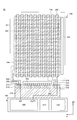
- FIG. 1 is a schematic plan view showing a configuration of an information processing device 10 and a host 500 according to an embodiment of the present invention.
- FIG. 2 is a schematic plan view showing the configuration of the PUF-ID extraction circuit 380 according to the embodiment of the present invention.
- the information processing device 10 is a device using PUF.
- the information processing device 10 includes an electronic device 100 and an integrated circuit 300.
- the electronic device 100 is electrically connected to the integrated circuit 300.
- the information processing device 10 is electrically connected to the host 500.
- the information processing device 10 is a semiconductor integrated circuit.
- the information processing device 10 may be connected to the host 500 by bidirectional communication via a wireless network.
- the information processing device 10 can be carried around.
- the electronic device 100 may be a display device, a device that combines a device capable of displaying an image and a touch panel, or an image pickup device having an image sensor.
- the electronic device 100 may be a device that does not display an image, such as a touch panel alone, a storage device such as a non-volatile memory or a volatile memory.
- the touch panel may be an in-cell touch panel built in the display device or an out-cell touch panel externally attached to the display device.
- the electronic device 100 included in the information processing device 10 may have a value having different physical characteristics for each measurement object such as an element included in the electronic device 100.
- the host 500 is a computer that provides an application or a program to the information processing device 10 via a wireless network. For example, when the information processing device 10 requests the host 500 to provide an application, the host 500 provides the application installation file to the information processing device 10. The user can install the application on the information processing device 10 and use the application installed on the information processing device 10. For example, when the host 500 receives a request from the user or the information processing device 10 regarding the provision of an application or program related to the operation mode, the host 500 provides the information processing device 10 with an installation file or program of the application. As a result, the user can install the application in the information processing device 10 and use the application installed in the information processing device 10 to cause the information processing device 10 to execute the program related to the operation mode.
- the integrated circuit 300 includes a mode selection circuit 310, a signal generation circuit 320, an integration circuit 330, an S / H circuit and an AD conversion circuit 340, an averaging circuit 350, a storage circuit 360, a control circuit 370, and a PUF-ID extraction circuit 380. ..
- the information processing device 10 includes at least two operation modes, a normal operation mode and a PUF operation mode.
- the mode selection circuit 310 can select either a normal operation mode or a PUF operation mode.
- the mode selection circuit 310 may include an arithmetic processing circuit and a storage circuit.
- the mode selection circuit 310 reads a program from the storage circuit, and processes signals, voltages, data, and the like by the arithmetic processing circuit based on the read program.
- the normal operation mode is a mode in which the electronic device 100 originally has an operation.
- the normal operation mode is a mode in which the characteristics of each element included in the electronic device 100 are detected, and the information processing apparatus 10 performs a new process based on the detection result.
- the normal operation mode is a mode in which the characteristics of each element included in the electronic device 100 are detected, the detection result is output to the host 500, the detection result is analyzed by the host 500, and the analysis result is fed back to the electronic device 100. is there.
- the PUF operation mode is a mode in which the characteristics of each element included in the electronic device 100 are detected and an identifier (ID) unique to the information processing device 10 is generated based on the detection result. is there.
- ID identifier
- the mode selection circuit 310 transfers data such as the number of the measurement object included in the electronic device 100 or the measurement object included in the electronic device 100 from the host 500 or the user (not shown), and is transferred. Processing may be performed based on the data. That is, the mode selection circuit 310 may perform the above processing based on the instruction of the host 500 or the user (not shown).
- the arithmetic processing circuit is, for example, a processor, a CPU, or the like.
- the information processing apparatus 10 By having the PUF-ID extraction circuit 380, the information processing apparatus 10 according to the embodiment of the present invention utilizes the electronic device 100 or the physical characteristics having different values for each element included in the electronic device 100. Different information can be generated for each element.
- the information processing device 10 according to the embodiment of the present invention can use different information for each element generated by the PUF-ID extraction circuit 380 as an identifier (Identifier, ID) unique to the information processing device 10. Therefore, since the information processing device 10 according to the embodiment of the present invention is distinguished from a counterfeit product, a pirated version, or a counterfeit product of the information processing device 10, the information processing device 10 according to the embodiment of the present invention is PUF-.
- ID extraction circuit 380 it is possible to prevent the production of a counterfeit product, a pirated version, or a counterfeit product of the information processing apparatus 10.
- the information processing device 10 detects the characteristics of each element included in the electronic device 100 by having the control circuit 370, and the information processing device 10 performs a new process based on the detection result. be able to. Further, the information processing device 10 according to the embodiment of the present invention can detect the characteristics of each element included in the electronic device 100 and feed back the detection result to the electronic device 100 by having the control circuit 370. ..
- the control circuit 370 may have an arithmetic processing circuit and a storage circuit. The control circuit 370 reads a program from the storage circuit, and processes signals, voltages, data, and the like by the arithmetic processing circuit based on the read program.
- the signal generation circuit 320 generates, for example, a drive signal for driving the control circuit 370.
- the signal generation circuit 320 is electrically connected to the electronic device 100. Further, the signal generation circuit 320 may be electrically connected to each circuit included in the integrated circuit 300.
- the signal generation circuit 320 has an arithmetic processing circuit, and the driving signal may be generated by the arithmetic processing circuit.
- the drive signal may be output from the signal generation circuit 320 and input to the electronic device 100, or may be output from the signal generation circuit 320 and input to each circuit included in the integrated circuit 300.
- the integrator circuit 330 can obtain the result of integrating the input signal or the input voltage in a predetermined time as the output signal or the output voltage.
- the integrator circuit 330 is electrically connected to the electronic device 100.
- the integrated circuit 300 has the integrating circuit 330, it is possible to obtain the result of integration in a predetermined time by using the output signal or the output voltage from each element included in the electronic device 100 as the input signal or the input voltage. Therefore, the characteristics of each element included in the electronic device 100 can be detected.
- the output signal or output voltage output by the integrating circuit 330 is an analog signal or analog voltage.
- the S / H circuit and the AD conversion circuit 340 can accumulate an electric charge corresponding to an analog signal or an analog voltage and convert it into a digital signal.
- the S / H circuit and the AD conversion circuit 340 are electrically connected to the integrating circuit 330.
- the S / H circuit and the AD conversion circuit 340 can obtain the result of converting the signal or voltage output from the integrating circuit 330 into a digital signal as an input signal or input voltage. Therefore, the characteristics of each element included in the electronic device 100 can be detected.
- the information processing device 10 may have two or more S / H circuits and AD conversion circuits 340, and may be able to acquire two or more analog signals or analog voltages in parallel. That is, the two or more S / H circuits and the AD conversion circuit 340 may be capable of inputting two or more analog signals or analog voltages in parallel.
- the averaging circuit 350 is a circuit that acquires digital signals a plurality of times in a predetermined period and averages the acquired digital signals a plurality of times. Further, the averaging circuit 350 may be a circuit that acquires two or more digital signals a plurality of times in a predetermined period and averages each of the acquired digital signals a plurality of times. Further, the averaging circuit 350 may store a plurality of input digital signals. The averaging circuit 350 is electrically connected to the S / H circuit and the AD conversion circuit 340. The averaging circuit 350 has an arithmetic processing circuit, and the arithmetic processing circuit averages digital signals. Further, the averaging circuit 350 may have a circuit for storing the averaging digital signal.
- the averaging circuit 350 may have an arithmetic processing circuit and a storage circuit.
- the averaging circuit 350 reads a program from the storage circuit, and based on the read program, averages the digital signal by the arithmetic processing circuit. Further, the averaging circuit 350 may store the averaging digital signal in the storage circuit.
- the circuit or device that stores the digital signal is, for example, a storage circuit.
- the storage circuit is preferably a volatile memory typified by SRAM or DRAM.
- the integrated circuit 300 has the averaging circuit 350, noise or variation of the analog signal or analog voltage is removed or alleviated, and the conversion resolution of the analog signal or analog voltage is improved. As a result, the detection accuracy of the control circuit 370 and the detection accuracy of each ID output by the PUF-ID extraction circuit 380 are improved.
- the storage circuit 360 can store the digital signal output from the averaging circuit 350.
- the storage circuit 360 is electrically connected to the control circuit 370. Further, the storage circuit 360 may be electrically connected to the PUF-ID extraction circuit 380. Since the storage circuit 360 is electrically connected to the control circuit 370 or the PUF-ID extraction circuit 380, the digital signal averaged by the averaging circuit 350 is not directly supplied to the host 500. Therefore, in the information processing device 10, it is possible to prevent the characteristics of each element included in the electronic device 100 from leaking to the host 500. Further, it is possible to prevent a third party who has obtained the leaked characteristic from the leaked characteristic from generating an ID unique to the information processing apparatus 10.
- the PUF-ID extraction circuit 380 includes, for example, a frame averaging processing circuit 382, a determination circuit 384, an ID selection circuit 386, a noise removal circuit 388, a cryptographic circuit 390, and an extraction circuit 392.
- the PUF-ID extraction circuit 380 is supplied with a digital signal output from the storage circuit 360.
- the PUF-ID extraction circuit 380 generates an ID unique to the information processing device 10 by processing the digital signal. Based on the instructions of the host 500 or the user (not shown), the ID unique to the generated information processing device 10 is supplied to the host 500 or the user.
- the frame averaging processing circuit 382 can calculate and output the average value of the digital signal at a predetermined time.
- the frame averaging processing circuit 382 is electrically connected to the storage circuit 360 and the determination circuit 384.
- the digital signal output from the storage circuit 360 is supplied to the frame averaging processing circuit 382 as an input signal or an input voltage.
- the signal or voltage output from the frame averaging processing circuit 382 to the determination circuit 384 is also a digital signal.
- the frame averaging processing circuit 382 may include an arithmetic processing circuit and a storage circuit.
- the frame averaging processing circuit 382 reads a program from the storage circuit, determines the average number of frames based on the read program, and acquires an input signal or an input voltage corresponding to each of the average number of frames.
- the frame averaging processing circuit 382 performs averaging processing of the input signal or the input voltage corresponding to each of the average number of frames. Further, the frame averaging processing circuit 382 may store the averaging-processed input signal or input voltage in the storage circuit. Further, the frame averaging processing circuit 382 supplies the averaging-processed input signal or input voltage to the determination circuit 384.
- the predetermined time is, for example, the time from when the nth image is displayed on the electronic device 100 until the n + 1th image is displayed. A given time is sometimes called a period. Also, a predetermined time or period is called a frame.
- the frame averaging processing circuit 382 can acquire the input signal or the input voltage for K frames and average the acquired input signal or the input voltage for the K frames.
- K is a natural number.
- the frame averaging processing circuit 382 can average the noise or variation contained in the input signal or the input voltage in the same manner as the averaging circuit 350 described above. That is, when the PUF-ID extraction circuit 380 has the frame averaging processing circuit 382, noise or variation contained in the input signal or the input voltage is removed or alleviated. Therefore, the conversion resolution of the signal or voltage is improved. As a result, the detection accuracy of each ID output by the PUF-ID extraction circuit 380 is improved. Further, as the storage circuit included in the frame averaging processing circuit 382, the same circuit as the storage circuit 360 can be used.
- the determination circuit 384 determines, for example, whether the digital signal frame averaging processed by the frame averaging processing circuit 382 is an even number or an odd number.
- the determination circuit 384 may include an arithmetic processing circuit and a storage circuit.
- the determination circuit 384 may read a program from the storage circuit or the host 500, and process the digital signal by the arithmetic processing circuit based on the read program. Further, the determination circuit 384 may store the digital signal processed by the arithmetic processing circuit in the storage circuit.
- the determination circuit 384 may set the determination result to 0 when the digital signal is an even number.
- the determination circuit 384 may set the determination result to 1 when the digital signal is an odd number.
- the frame averaging processed digital signal may be referred to as an averaging processed signal.
- the determination result is referred to as a response
- the ID unique to the information processing apparatus 10 is referred to as a response ID.
- the determination circuit 384 has a storage circuit, and the response and the response ID may be stored in the storage circuit of the determination circuit 384. Further, the response and the response ID may be supplied from the determination circuit 384 to the ID selection circuit 386 and stored in the ID selection circuit 386.
- the arithmetic processing circuit is, for example, a processor, a CPU, or the like. Further, as the storage circuit included in the determination circuit 384, the same circuit as the storage circuit 360 can be used. When a plurality of input signals or input voltages are input to the integrated circuit 300, the determination circuit 384 generates a response for each of the plurality of input signals or input voltages.
- the determination method of the determination circuit 384 shown in the present specification and the like is an example, and is not limited to this example.
- the determination circuit 384 may set the determination result to 1 when the digital signal is an even number, and set the determination result to 0 when the digital signal is an odd number.
- the determination circuit 384 may determine whether the value is large or small with respect to the threshold value based on a predetermined threshold value.
- the ID selection circuit 386 generates an ID unique to the information processing device 10, that is, a response ID. Further, the ID selection circuit 386 supplies the selected response ID (IDA) to the noise reduction circuit 388 or the extraction circuit 392. For example, the ID selection circuit 386 receives a number of a measurement object included in the electronic device 100 or a measurement object included in the electronic device 100 designated by the host 500 or a user (not shown). For example, when the ID selection circuit 386 receives the number of the measurement object, it selects all the responses corresponding to the number of the measurement object from the plurality of stored responses. Then, the ID selection circuit 386 connects all the responses to generate a response ID of the number of the object to be measured.
- IDA selected response ID
- the ID selection circuit 386 When the ID selection circuit 386 receives the number of the measurement target, the ID selection circuit 386 selects a response ID (IDA) corresponding to the number of the measurement target from the plurality of stored response IDs, and sets the IDA as a noise removal circuit. Supply to 388 or extraction circuit 392.
- the ID selection circuit 386 may be connected to the host 500.
- the ID selection circuit 386 may include an arithmetic processing circuit and a storage circuit.
- the ID selection circuit 386 may read a program from the storage circuit and perform the processing by the arithmetic processing circuit based on the read program.
- the noise removal circuit 388 removes noise included in the supplied response ID. Specifically, when the IDA is supplied from the ID selection circuit 386, the noise removal circuit 388 removes the noise contained in the IDA. Since the IDA may contain noise, the noise reduction circuit 388 can generate a noise-removed ID (IDB) by providing the noise reduction circuit 388 in the PUF-ID extraction circuit 380. .. For example, when the response and response ID are used for a private key such as encryption, noise removal is indispensable. Therefore, if the noise removal circuit 388 is provided in the PUF-ID extraction circuit 380, noise is removed from the response and response ID. It is an effective means for removing. The noise reduction circuit 388 also supplies the IDB to the encryption circuit 390 or the extraction circuit 392. The noise reduction circuit 388 may be connected to the host 500.
- IDB noise-removed ID
- the encryption circuit 390 encrypts the supplied response ID. Specifically, when the IDB is supplied from the noise removal circuit 388, the encryption circuit 390 encrypts the IDB and generates an encrypted ID (IDC). For example, when the response and response ID are used as a private key for encryption or the like, providing the noise removal circuit 388 in the encryption circuit 390 is an effective means for encrypting the response and response ID.
- the encryption circuit 390 also supplies the IDC to the extraction circuit 392.
- the encryption circuit 390 may be connected to the host 500. For example, the encryption circuit 390 encrypts the supplied IDB with another ID (private key) from which noise has been removed to generate an IDC. Further, for example, the encryption circuit 390 may encrypt the supplied IDB with a hash function to generate an IDC.
- the extraction circuit 392 extracts at least one ID from the supplied IDA, IDB, or IDC, and supplies the extracted ID to the host 500 or the user. For example, the extraction circuit 392 extracts the IDA and supplies the IDA to the host 500 or the user.
- the host 500 may have the function of the extraction circuit 392.
- the ID selection circuit 386 supplies the IDA to the host 500 or the user
- the noise reduction circuit 388 supplies the IDB to the host 500 or the user
- the encryption circuit 390 supplies the IDA to the host 500 or the user.
- the IDC is supplied to the host 500 or the user.
- the input from the electronic device 100 to the integrated circuit 300, the input from the integrated circuit 300 to the electronic device 100, and the integrated circuit 300 Although the input / output to and from the host 500 is shown to be one, a plurality of signals, voltages or information may be input or output in parallel between the devices.
- the configuration of the information processing device 10 according to the embodiment of the present invention shown in FIGS. 1 and 2 is an example, and is not limited to this configuration.
- the ID unique to the information processing device 10 acquires the characteristics of the element included in the electronic device 100 a plurality of times, averages the acquired characteristics by the averaging circuit 350, and processes them by the PUF-ID extraction circuit 380. I just need to be able to get it.
- the ID unique to the information processing device 10 acquires the characteristics of a plurality of elements included in the electronic device 100, averages the acquired characteristics by the averaging circuit 350, and processes them by the PUF-ID extraction circuit 380. It suffices if it can be obtained by.
- the information processing device 10 by providing the PUF-ID extraction circuit 380, the measurement object included in the electronic device 100 included in the information processing device 10 or the measurement included in the electronic device 100 An ID unique to the information processing device 10 can be generated by utilizing the characteristics of the electronic device 100 such as the number of the object. Further, the information processing apparatus 10 according to the embodiment of the present invention generates a response ID by the PUF-ID extraction circuit 380 when the host 500 inquires about the response ID, and sends the generated response ID to the host 500. Can be provided. Therefore, the information processing device 10 according to the embodiment of the present invention does not generate a response ID unless the host 500 inquires about the response ID.
- a non-volatile memory is mounted and the private key or ID is always stored in the non-volatile memory.
- the ID is less likely to be stolen or forged compared to an information processing device that stores the unique information of.
- the information processing apparatus 10 according to the embodiment of the present invention can prevent the production of counterfeit products. Therefore, the information processing device 10 according to the embodiment of the present invention has theft of the ID or the ID as compared with the device in which the non-volatile memory is mounted and the unique information such as the private key or the ID is stored in the non-volatile memory. Hard to be counterfeited. As a result, the information processing apparatus 10 according to the embodiment of the present invention can prevent the production of counterfeit products.
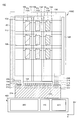
- FIG. 3 is a plan view showing a part of the configuration of the information processing apparatus 10 according to the embodiment of the present invention.
- the electronic device 100 is a touch panel having a touch electrode will be described. Description of the same or similar configuration as that of FIG. 1 or 2 may be omitted.
- the information processing device 10 includes an electronic device 100, a circuit board 400, and a connector 214.
- the electronic device 100 has a plurality of first touch electrodes 294 arranged in parallel with the X direction (row direction) in the top view, and a second touch electrode 294 arranged in parallel with the Y direction (column direction) in the top view. It has an electrode 292, a first substrate 20, a display unit 122, a peripheral unit 136, a video signal line drive circuit 124, and a scanning signal line drive circuit 126.
- the touch panel has tx first touch electrodes 294 and ty second touch electrodes 292
- the coordinates of the intersection of the first touch electrode 294 and the second touch electrode 292 (tx, ty).
- tx and ty are natural numbers.
- the electronic device 100 may have scanning signal line drive circuits on both the left and right sides in a top view.
- the electronic device 100 may be a touch panel alone as described above, or may be a device capable of displaying an image.
- the electronic device 100 may be a liquid crystal display device, a self-luminous display device such as an organic electroluminescence (EL) or a micro LED, an electrophoresis display device, or the like. May be good.
- EL organic electroluminescence
- micro LED micro LED
- electrophoresis display device or the like. May be good.
- the display unit 122 has a plurality of pixel circuits. The details of the pixel circuit will be described later.
- the video signal line drive circuit 124 and the scanning signal line drive circuit 126 are provided in the peripheral portion 136.
- the video signal line drive circuit 124 is provided at positions adjacent to each other, for example, in parallel or substantially parallel to the Y direction.
- the scanning signal line drive circuit 126 is provided at positions adjacent to each other, for example, in parallel or substantially parallel to the X direction.
- the video signal line drive circuit 124 and the scanning signal line drive circuit 126 control the drive of pixels.
- the video signal line drive circuit 124 and the scanning signal line drive circuit 126 show an example in which an IC chip is used. Further, in FIG.
- a drive circuit formed on a substrate (semiconductor substrate or the like) different from the first substrate 20 is placed on a connector 214 such as a first substrate 20 or a flexible printed circuit (Flexible Printed Circuit, FPC) substrate. It may be provided. Further, a part or all of the circuits included in the video signal line drive circuit 124 and the scanning signal line drive circuit 126 are formed on a substrate different from the first substrate 20, and on the first substrate 20 or the connector 214. It may be provided. Further, the drive circuit or a part of the drive circuit included in the scanning signal line drive circuit 126 may be formed directly on the first substrate 20. On the first substrate 20, display elements such as liquid crystal elements provided in the pixels and various semiconductor elements for controlling them are formed.
- the electronic device 100 includes a first wiring 206, a contact hole 208, a first terminal wiring 210, a first terminal 212, a second wiring 216, a contact hole 218, a second terminal wiring 220, and a second. It also has terminals 222 and the like. These are also provided on the first substrate 20.
- the first touch electrode 294 is electrically connected to the first wiring 206 extending from the peripheral portion 136.
- a signal or power source for driving the pixel is supplied to the pixel from an external device (not shown) via the first terminal 212, the video signal line drive circuit 124 or the scanning signal line drive circuit 126. May be good.
- the first wiring 206 extends the peripheral portion 136 and is electrically connected to the first terminal wiring 210 via the contact hole 208.
- the first terminal wiring 210 is exposed near the end of the electronic device 100 on the side where the terminal electrode 240 is provided, and forms the first terminal 212.
- the first terminal 212 is connected to the connector 214.
- the second touch electrode 292 is electrically connected to the second wiring 216 extending from the peripheral portion 136.
- a signal or power source for driving the pixel may be supplied to the pixel via an external device (not shown) and a second wiring 216 extending from the peripheral portion 136.
- the second wiring 216 extends the peripheral portion 136 and is electrically connected to the second terminal wiring 220 via the contact hole 218.
- the second terminal wiring 220 is exposed near the end of the electronic device 100 on the side where the terminal electrode 240 is provided to form the second terminal 222.
- the second terminal 222 is connected to the connector 214.
- the first terminal 212 or the second terminal 222 can be formed so as to line up on one side of the electronic device 100. Therefore, using a single connector 214, a signal for touch detection and a signal when touch is performed are supplied to the first touch electrode 294 and the second touch electrode 292, and a voltage or a signal is supplied. Can be supplied to each of the display unit 122, the video signal line drive circuit 124, and the scanning signal line drive circuit 126.
- the circuit board 400 includes, for example, an integrated circuit 300, a signal supply circuit 410, and a power supply circuit 420.
- the circuit board 400 is electrically connected to the electronic device 100 via the connector 214.
- the signal supply circuit 410 generates signals supplied to the display panel, such as a video signal and a timing signal that controls the operation of the circuit. Further, the power supply circuit 420 supplies power to the integrated circuit 300 and the signal supply circuit 410.
- the connector 214 supplies a video signal, a timing signal for controlling the operation of the circuit, a power supply, and the like to the display unit 122, the video signal line drive circuit 124, and the scanning signal line drive circuit 126.
- the signal generation circuit 320 included in the integrated circuit 300 can generate one or more signals for touch detection.
- the generated signals may be a plurality of the same signals, a plurality of signals different from each other, or a plurality of signals different from each other with the same signal.
- the drive of the touch panel will be briefly described by taking the mutual capacitance method as an example.
- the mutual capacitance method when a human finger touches the electronic device 100, the parasitic capacitance in the first touch electrode 294 and the second touch electrode 292 is obtained from the human finger and the first touch electrode 294 and the second. The capacitance generated between the touch electrode 292 and the touch electrode 292 is subtracted. By reading this change, the position where the human finger touches the electronic device 100 is detected.
- the drive of the touch panel is not limited to this example.
- the touch panel may be driven by a self-capacity method.
- the user when detecting the position where a human finger touches the electronic device 100, the user selects an application for detecting the touch position.
- the information processing apparatus 10 selects a normal operation mode and operates the control circuit 370.
- the signal (drive signal) for touch detection generated by the signal generation circuit 320 is transmitted from the IN1 terminal of the integrated circuit 300 to the connector 214, the first terminal 212, the first terminal wiring 210, and the contact hole. It is supplied to the first touch electrode 294 via 208 and the first wiring 206. Further, for example, a signal (touch signal) based on a change when the touch panel is touched by a person is transmitted from the second touch electrode 292 to the second wiring 216, the contact hole 218, the second terminal wiring 220, and the second. It is supplied to the OUT1 terminal of the integrated circuit 300 via the terminal 222 and the connector 214 of.
- a signal (non-touch signal) at which the intersection of the first touch electrode 294 and the second touch electrode 292 is not touched is transmitted from the second touch electrode 292 to the second wiring 216, the contact hole 218, and the second. It is supplied to the OUT1 terminal of the integrated circuit 300 via the terminal wiring 220 of 2 and the second terminal 222 and the connector 214. The signal supplied to the OUT1 terminal is converted into an averaged digital signal via the integrating circuit 330, the S / H circuit, the AD conversion circuit 340, and the averaging circuit 350, and stored in the storage circuit 360. Then, the control circuit 370 detects the position where the human finger touches the electronic device 100.
- the information processing device 10 selects the PUF operation mode.
- the detected result is supplied to the PUF-ID extraction circuit 380.
- the digital signal generated by the S / H circuit and the AD conversion circuit 340 does not go through the averaging circuit 350 and the storage circuit 360, but the S / H circuit and the storage circuit 360. It may be transferred directly from the H circuit and the AD conversion circuit 340 to the control circuit 370.
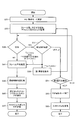
- FIG. 4 is a flowchart showing a driving method of the information processing apparatus 10 according to the embodiment of the present invention. The description may be omitted for the same or similar configurations as those in FIGS. 1 to 3.
- the electronic device 100 is a touch panel having a touch electrode.
- a signal for selecting the PUF operation mode is transferred from the host 500 or the user to the integrated circuit 300.
- transferring a signal can be rephrased as supplying a signal.
- the transfer of a signal may be rephrased as the provision of a signal or the input of a signal.
- the signal may be a voltage.
- step 33 the number of frames to be averaged, the number of digits or bits of the digital signal for determining even or odd numbers, and the first touch electrode 294 and the second touch electrode
- the address is transferred from the host 500 or the user to the integrated circuit 300.
- the number of frames to be averaged, the number of digits or bits of the digital signal for determining even or odd numbers, and the addresses of the first touch electrode 294 and the second touch electrode are the storage circuits of the integrated circuit 300 ( It is stored in (not shown) and set.
- the number of digits or the number of bits of the digital signal for determining an even or odd number is, for example, 4 of the 8-bit digital signals when the number of the element included in the electronic device 100 is an 8-bit digital signal.
- a signal or voltage such as an address between the first touch electrode and the second touch electrode, an address of a pixel circuit included in a display device, an address indicating a storage element number included in a storage circuit, and the like.
- the number or coordinates indicating the element or the object to be measured that outputs the above is called a challenge.
- the challenge may be one or two.
- the number of frames to be averaged and the number of digits or bits of the digital signal for determining even numbers or odd numbers can be appropriately set depending on the use and specifications of the response ID.
- step 35 the information processing device 10 detects whether or not the touch panel is touched by a person. Since the PUF operation mode is selected in step 31 (S31), the control circuit 370 and the PUF-ID extraction circuit 380 are driven. In order to detect whether or not the touch panel is touched by a person, the touch signal or the non-touch signal is sent from the electronic device 100 via OUT1 to the integrating circuit 330, the S / H circuit and the AD conversion circuit 340, and averaging. It is processed by the circuit 350 and stored in the storage circuit 360. The control circuit 370 reads the processed touch signal or non-touch signal from the storage circuit 360. The control circuit 370 detects the touch position by processing the read signal.
- control circuit 370 when the control circuit 370 processes the touch signal, it detects the addresses of the first touch electrode 294 and the second touch electrode indicating the position touched by the user (YES). When the control circuit 370 processes the non-touch signal, the control circuit 370 detects that "the user has not touched the panel" (NO). The drive related to NO will be described later.
- control circuit 370 confirms the number of detections in step 37 (S37). Here, the control circuit 370 calculates the number of detected touch positions.
- the control circuit 370 supplies the display control signal to the signal supply circuit 410.
- LN, L1, and L2 are natural numbers, and L2 is larger than L1.
- the signal supply circuit 410 supplies the image data related to the first warning to the display unit 122.
- the display unit 122 displays an image related to the first warning, and the information processing device 10 again executes step 33 (S33).
- the warning display is, for example, an indication that the screen should not be touched.
- step 39 S39).
- the drive in which the information processing apparatus 10 executes steps 39 (S39) to 33 (S33) again is referred to as a repeat challenge (RC).
- RC repeat challenge
- the information processing apparatus 10 changes the addresses of the first touch electrode 294 and the second touch electrode ( A signal requesting (change of challenge) and an address (detection address) between the first touch electrode 294 and the second touch electrode corresponding to the detected touch position may be transmitted to the host 500.
- the host 500 when the host 500 receives the signal requesting the change of the challenge and the detection address, the host 500 processes the information processing by using the addresses of the first touch electrode 294 and the second touch electrode whose touch position is not detected as a challenge. It may be transmitted to the device 10. Further, for example, the addresses of the first touch electrode 294 and the second touch electrode excluding the addresses around the detection address may be used as a challenge and transmitted to the information processing apparatus 10.
- step 37 (S37) when the detection number LN is smaller than L1, or S37 is executed via RC and the detection number LN is smaller than L2, the control circuit 370 is set to step 41 (S41). To execute. Step 41 (S41) will be described later. Further, in step 37 (S37), when the detection number LN is L2 or more, the control circuit 370 executes step 51 (S51). Step 51 (S51) will be described later.
- step 51 the signal supply circuit 410 supplies the image data related to the second warning to the display unit 122.
- the display unit 122 displays an image related to the second warning. Similar to the first warning, the warning display is, for example, a display saying that the screen should not be touched.
- N be the number of times the warning is displayed, and let R be the preset number of times. N and R are natural numbers.
- step 33 S33 is executed again.
- N is R or more
- the PUF operation mode is terminated (step 53 (S53)).
- a signal indicating that the PUF operation mode has ended is transmitted from the integrated circuit 300 to the host 500 (step 55 (S55)). That is, the File signal is transmitted from the integrated circuit 300 to the host 500. Then, the operation of the information processing device 10 is completed.
- the frame averaging processing circuit 382 executes the frame averaging process in step 41 (S41).
- a signal (non-touch signal) in which the intersection of the first touch electrode 294 and the second touch electrode 292 is not touched is input to the integrating circuit 330, and is digitally signaled by the S / H circuit and the AD conversion circuit 340. Is converted to.
- the non-touch signal is converted into a 12-bit digital signal. That is, the non-touch signal takes any one of 1 to 4096 when expressed in decimal notation.
- the averaging circuit 350 acquires the non-touch signals a plurality of times in one frame, and averages the acquired plurality of non-touch signals. For example, in step 33, when the number of frames to be averaged is set to 60, the non-touch signal is acquired a plurality of times in each of the 60 frames, and the acquired plurality of non-touch signals are averaged. The average.
- the signal averaged in each of the 60 frames is stored in the storage circuit 360. Subsequently, the signal averaged in each of the 60 frames is transferred to the storage circuit 360 or the frame averaging processing circuit 382, and the frame averaging process is executed.
- the operation described above is performed at all addresses selected by the first touch electrode 294 and the second touch electrode 292.
- the above is step 41 (S41).
- step 43 (S43) the even / odd number determination process is executed by the determination circuit 384.
- the determination circuit 384 determines 2000 as an even number and sets the determination result to 0.
- the determination result 0 is the response of the address corresponding to the processed digital signal.
- the determination circuit 384 may store the response in the storage circuit included in the determination circuit 384. Further, the determination circuit 384 may supply the response to the ID selection circuit 386. The operation described above is executed for all the digital signals processed for frame averaging. The above is step 43 (S43).
- step 45 the response ID (IDA) is generated by the ID selection circuit 386.
- the ID selection circuit 386 it is assumed that a plurality of addresses of the first touch electrode 294 and the second touch electrode are set. That is, it is assumed that a plurality of challenges are set in step 33.
- the ID selection circuit 386 is supplied with a plurality of responses from the determination circuit 384, and the plurality of responses are stored in the storage circuit included in the ID selection circuit 386.
- the ID selection circuit 386 reads the response corresponding to each of the plurality of challenges from the storage circuit.
- the ID selection circuit 386 connects all the read responses to generate a response ID.
- step 33 eight addresses of the first touch electrode 294 and the second touch electrode are set, and the response to each address is 0, 0, 1, 1, 1, 1, 1, 0. And.
- the ID selection circuit 386 reads the responses 0, 0, 1, 1, 1, 1, 1, 0 from the storage circuit and connects them to generate the IDA 001111110.
- the ID selection circuit 386 supplies the IDA to the noise reduction circuit 388 and the extraction circuit 392.
- step 45 (S45) the response IDB is generated by the noise reduction circuit 388.
- the noise reduction circuit 388 removes the noise contained in the IDA.
- the noise reduction circuit 388 generates an ID (IDB) in which noise is removed from the IDA.
- the noise reduction circuit 388 supplies the IDB to the encryption circuit 390 and the extraction circuit 392.
- the response ID (IDC) is generated by the encryption circuit 390.
- the encryption circuit 390 encrypts the IDB and generates an encrypted ID (IDC).
- the cryptographic circuit 390 supplies the IDC to the extraction circuit 392.
- step 47 when the extraction circuit 392 receives the IDA, IDB, and IDC, at least one ID is extracted from the IDA, IDB, or IDC.
- the extraction circuit 392 supplies the extracted ID to the host 500 or the user.
- the extraction circuit 392 extracts the IDA and transmits the IDA to the host 500 or the user.
- the response ID may be registered in the host 500 or the user. Then, the operation of the information processing device 10 is completed.
- the information processing apparatus by providing the PUF-ID extraction circuit, for example, a signal when the touch electrode included in the information processing apparatus is not touched can be obtained. It can be used to generate an ID unique to the information processing device. Further, the information processing device according to the embodiment of the present invention is unique to the information processing device based on a signal in which noise and variation are suppressed by executing an averaging process in an integrated circuit having a PUF-ID extraction circuit. ID can be generated. Further, the information processing apparatus according to the embodiment of the present invention has an ID unique to the information processing apparatus based on a signal in which noise and variation are further suppressed by executing an averaging process also in the PUF-ID extraction circuit. Can be generated.
- the information processing device can generate a highly accurate unique ID by utilizing the characteristics of the semiconductor device included in the information processing device. Therefore, the information processing apparatus provided with the integrated circuit having the PUF-ID extraction circuit according to the embodiment of the present invention can prevent the production of counterfeit products.
- the information processing device 10B includes a liquid crystal display device 100B. Further, in one embodiment of the present invention, the information processing device 10B uses the characteristics of the pixel circuit of the liquid crystal display device 100B to generate the response ID of the information processing device 10B. The description of the same or similar configuration as in FIGS. 1 to 4 may be omitted.
- FIG. 5 is a schematic plan view showing the configuration of the information processing device 10B according to the embodiment of the present invention.
- FIG. 5 shows an example in which the electronic device 100 is a liquid crystal display device 100B as compared with FIG. The same or similar configurations as those in FIGS. 1 to 4 will not be described here.
- the liquid crystal display device 100B has at least a seal portion (not shown) and a second substrate 90 in addition to the configuration shown in FIG.
- the first substrate 20 and the second substrate 90 are bonded to each other by a seal portion.
- the display unit 122 is surrounded by a seal unit.
- a plurality of pixel circuits PXA are arranged in a matrix.
- the array of the plurality of pixel circuits PXA is a striped array.
- Each of the plurality of pixel circuits PXA may correspond to, for example, three sub-pixels 130, sub-pixels 132, and sub-pixels 134. One pixel may be formed by three sub-pixels.
- the pixel circuit PXA is the smallest unit that constitutes a part of the image reproduced by the display unit 122.
- Each sub-pixel is provided with one display element.
- the display element is a liquid crystal element. The color corresponding to the sub-pixel is determined by the characteristics of the liquid crystal element or the color filter provided on the sub-pixel.
- the three sub-pixels 130, sub-pixels 132, and sub-pixels 134 can be configured to give different colors to each other.
- the sub-pixel 130, the sub-pixel 132, and the sub-pixel 134 can each be provided with a color filter layer that emits the three primary colors of red, green, and blue. Then, an arbitrary voltage or current is supplied to each of the three sub-pixels, and the liquid crystal display device 100B can display an image.
- the video signal line drive circuit 124 is connected to one end of a plurality of video signal lines 154.
- the plurality of video signal lines 154 are connected to a plurality of pixel circuits PXA arranged in the Y direction.
- the scanning signal line drive circuit 126 is connected to one end of a plurality of scanning signal lines 152.
- the plurality of scanning signal lines 152 are connected to a plurality of pixel circuits PXA arranged in the X direction.
- the video signal line drive circuit 124 receives video signals from a plurality of terminal electrodes 240.
- the scanning signal line drive circuit 126 selects the scanning signal line 152, and a voltage corresponding to the video signal is written to the pixel circuit PXA connected to the selected scanning signal line 152. In this way, the image is displayed on the display unit 122.
- the other end of the plurality of video signal lines 154 may be electrically connected to the first wiring 206 extending from the peripheral portion 136.
- the first wiring 206 extends the peripheral portion 136 and is electrically connected to the first terminal wiring 210 via the contact hole 208.
- the first terminal wiring 210 is exposed near the end of the liquid crystal display device 100B on the side where the terminal electrode 240 is provided, and forms the first terminal 212.
- the first terminal 212 is connected to the connector 214.
- the video signal line drive circuit 124 and the scanning signal line drive circuit 126 may be electrically connected to the second wiring 216 extending from the peripheral portion 136.
- the second wiring 216 extends the peripheral portion 136 and is electrically connected to the second terminal wiring 220 via the contact hole 218.
- the second terminal wiring 220 is exposed near the end of the liquid crystal display device 100B on the side where the terminal electrode 240 is provided to form the second terminal 222.
- the second terminal 222 is connected to the connector 214.
- a signal or power source for driving the pixel may be supplied to the pixel from an external device (not shown) via the second terminal 222.
- the mode selection circuit 310 when the normal operation mode is selected by the mode selection circuit 310, for example, the scanning signal line 152 is selected and the potential written in the pixel is transferred to the video signal line 154. read out. Further, the data written in the pixels by the control circuit 370 may be corrected based on the read potential, and the corrected data may be fed back to each pixel.
- the liquid crystal display device 100B includes a first touch electrode 294 and a second touch electrode, like the electronic device 100, and includes the first touch electrode 294 and the second touch electrode.
- the response ID of the information processing apparatus 10B may be generated and selected based on the address of. Further, the information processing apparatus 10B according to the embodiment of the present invention has two response IDs, a response ID based on the pixel circuit PXA and a response ID based on the addresses of the first touch electrode 294 and the second touch electrode. May be generated and selected. By allowing the PUF-ID extraction circuit to generate and select two response IDs, it is possible to further reduce information leakage.
- FIG. 6 is a circuit diagram showing a pixel circuit PXA according to an embodiment of the present invention. The same or similar configurations as those in FIGS. 1 to 5 will not be described here.
- the pixel circuit PXA includes elements such as a transistor 162, a holding capacity 164, and a liquid crystal element 166.
- the transistor 162 has a gate electrode 162G, a source electrode 162S, and a drain electrode 162D.
- the gate electrode 162G is connected to the scanning signal line 152.
- the source electrode 162S is connected to the video signal line 154.
- the drain electrode 162D is connected to one end of the holding capacity 164 and one end of the liquid crystal element 166.
- the other end of the holding capacity 164 and the other end of the liquid crystal element 166 are connected to, for example, the reference power line 168.
- the reference power line 168 is commonly provided in the plurality of pixel circuits PXA.
- a constant potential is applied to the reference power line 168 from, for example, a plurality of second terminals 222.
- the constant potential is, for example, 0V.
- the reference power supply line 168 may be referred to as, for example, a common power supply line, and one end of the holding capacity 164 connected to the reference power supply line 168 or one end of the liquid crystal element 166 may be referred to as a common electrode.
- the function as a source and the function as a drain of each electrode may be interchanged.
- the circuit configuration of the pixel circuit PXA is an example, and is not limited to this. Further, since the pixel circuit PXA can be driven by a commonly used driving method of a liquid crystal display device, the description thereof is omitted here.
- FIG. 4 Driving Method of Information Processing Device 10B
- the flowchart shown in FIG. 4 can be used.
- the addresses of the first touch electrode 294 and the second touch electrode 292 in the description of FIG. 4 are replaced with the addresses of the pixel circuit PXA, and the pixel circuit is used.
- An example of generating a response ID of the information processing apparatus 10B by utilizing the characteristics of the transistor 162 of the PXA will be described. The same or similar configurations as those in FIGS. 1 to 6 will be omitted here.
- step 31 (S31) is the same as the description of FIG. 4, the description here is omitted.
- step 33 the number of frames to be averaged, the number of digits or bits of the digital signal for determining even or odd numbers, and the address of the pixel circuit PXA are determined by the integrated circuit from the host 500 or the user. Transferred to 300. Further, each pixel circuit PXA is initialized.
- the initialization includes uniformly converting the image data written in each pixel circuit PXA into the same data. Specifically, it includes writing a voltage corresponding to 0 V or black to each pixel circuit PXA. By initialization, the characteristics of each pixel circuit PXA can be changed to a state in which the same data is written.
- a pixel provided at a position where n scanning signal lines 152 arranged parallel to the X direction in top view and m video signal lines 154 arranged parallel to the Y direction in top view intersect.
- the coordinates of the circuit PXA are the coordinates (n, m)
- the coordinates (n, m) are called the addresses of the pixel circuit PXA.
- the numerical value n and the numerical value m are natural numbers, respectively. Since the description other than that described here is the same as the description in step 33 (S33) of FIG. 4, the description here is omitted.
- step 35 (S35) the information processing device 10 detects whether or not the address of the pixel circuit PXA is output. Since the PUF operation mode is selected in step 31 (S31), the control circuit 370 and the PUF-ID extraction circuit 380 are driven. In order to detect whether or not the address of the pixel circuit PXA is output, the address signal or the address non-detection signal is sent from the electronic device 100 via OUT1 to the integrating circuit 330, the S / H circuit and the AD conversion circuit 340. And processed by the averaging circuit 350 and stored in the storage circuit 360. The control circuit 370 reads the processed address signal or address non-detection signal from the storage circuit 360. The control circuit 370 detects the address by processing the read signal.
- control circuit 370 when the control circuit 370 processes the address signal, it detects the address of the pixel circuit PXA (YES). When the control circuit 370 processes the address non-detection signal, the control circuit 370 detects that "the address of the pixel circuit PXA is not output" (NO). The drive related to NO will be described later.
- control circuit 370 confirms the number of detections in step 37 (S37).
- the control circuit 370 calculates the number of detected addresses of the pixel circuit PXA (the number of addresses of the pixel circuit PXA). Since the description other than that described here is the same as the description in step 37 (S37) of FIG. 4, the description here is omitted.
- step 39 (S39) is the same as the description of FIG. 4, the description here is omitted.
- the information processing apparatus 10 receives a signal requesting a change in the address of the pixel circuit PXA (change in challenge), and ,
- the address (detection address) of the detected pixel circuit PXA may be transmitted to the host 500.
- the host 500 may transmit the address of the undetected pixel circuit PXA as a challenge to the information processing apparatus 10.
- the address of the pixel circuit PXA excluding the addresses around the detection address may be used as a challenge and transmitted to the information processing apparatus 10.
- Step 51 (S51), step 53 (S53), and step 55 (S55)) are the same as the description of FIG. 4, so the description here is omitted.
- the information processing apparatus 10B executes step 41 (S41) in the case of NO in step 35 (S35).
- step 41 (S41) the frame averaging process is executed by the frame averaging processing circuit 382. Specifically, the address of the undetected pixel circuit PXA is selected, the voltage written in the selected pixel circuit PXA is read out, and the read voltage (first voltage) is input to the integrating circuit 330. It is converted into a digital signal by the S / H circuit and the AD conversion circuit 340. For example, when the S / H circuit and the AD conversion circuit 340 have a 12-bit AD conversion circuit, the first voltage is converted into a 12-bit digital signal. That is, the first voltage takes any one of 1 to 4096 when expressed in decimal notation.
- the averaging circuit 350 acquires the first voltage a plurality of times in one frame, and averages the acquired plurality of first voltages. For example, in step 33, when the number of frames to be averaged is set to 60, the first voltage is acquired a plurality of times in each of the 60 frames, and the acquired first voltage is averaged. To. The signal averaged in each of the 60 frames is stored in the storage circuit 360. Subsequently, the signal averaged in each of the 60 frames is transferred to the storage circuit 360 or the frame averaging processing circuit 382, and the frame averaging process is executed. The operation described above is executed at the addresses of all the selected pixel circuits PXA. The above is step 41 (S41).
- Subsequent steps 43 (S43), 45 (S45), and 47 (S47) are executed by replacing the addresses of the first touch electrode 294 and the second touch electrode with the addresses of the pixel circuit PXA. Will be done. Other than that, the description is the same as that of FIG. 4, so the description here is omitted.
- the information processing apparatus is provided with the PUF-ID extraction circuit, for example, by utilizing the characteristics of the pixel circuit included in the information processing apparatus. A unique ID can be generated for. Therefore, the information processing apparatus provided with the integrated circuit having the PUF-ID extraction circuit according to the embodiment of the present invention can prevent the production of counterfeit products. 3. 3. Third Embodiment
- the information processing device 10C has an EL display device 100C. Further, in one embodiment of the present invention, the information processing device 10C uses the characteristics of the pixel circuit of the EL display device 100C to generate a response ID of the information processing device 10C. The description of the same or similar configuration as in FIGS. 1 to 6 may be omitted.
- FIG. 7 is a schematic plan view showing the configuration of the information processing device 10C according to the embodiment of the present invention.
- FIG. 7 shows an example in which the electronic device 100 is the EL display device 100C as compared with FIG. The same or similar configurations as those in FIGS. 1 to 6 will be omitted here.
- the EL display device 100C has at least a seal portion (not shown) and a second substrate 288 in addition to the configuration shown in FIG.
- the first substrate 20 and the second substrate 288 are bonded to each other by a seal portion.
- the display element provided in each sub-pixel is a light emitting element.
- the video signal line drive circuit 124 is connected to one end of the plurality of video signal lines 154 and one end of the plurality of voltage measurement lines 156.
- the plurality of video signal lines 154 and the plurality of voltage measurement lines 156 are connected to a plurality of pixel circuits PXB arranged in the Y direction.
- one end of the plurality of scanning signal lines 152 and one end of the plurality of control signal lines 158 are connected to a plurality of pixel circuits PXB arranged in the X direction.
- the other end of the plurality of voltage measuring lines 156 may be electrically connected to the first wiring 206 extending from the peripheral portion 136.
- the first wiring 206 extends the peripheral portion 136 and is electrically connected to the first terminal wiring 210 via the contact hole 208.
- the first terminal wiring 210 is exposed near the end of the EL display device 100C on the side where the terminal electrode 240 is provided, and forms the first terminal 212.
- the first terminal 212 is connected to the connector 214.
- the configuration of the information processing device 10C is the same as the configuration of FIG. 5 except for the configuration described with reference to FIG. 7, so the description here is omitted.
- the EL display device 100C also includes a first touch electrode 294 and a second touch electrode like the electronic device 100 and the liquid crystal display device 100B, and the first touch electrode 294 and the first touch electrode 294 and the first touch electrode.
- the response ID of the information processing device 10C may be generated and selected based on the address of the touch electrode of 2.
- the information processing apparatus 10B according to the embodiment of the present invention has two response IDs, a response ID based on the pixel circuit PXB and a response ID based on the addresses of the first touch electrode 294 and the second touch electrode. May be generated and selected. By allowing the PUF-ID extraction circuit to generate and select two response IDs, it is possible to further reduce information leakage.
- FIG. 8 is a circuit diagram showing a pixel circuit PXB according to an embodiment of the present invention. The same or similar configurations as those in FIGS. 1 to 7 will be omitted here.
- the pixel circuit PXB includes a drive transistor 264, a selection transistor 262, a voltage measurement transistor 270, a light emitting element 266, and a holding capacity 268.
- the gate electrode of the drive transistor 264 is connected to the drain electrode of the selection transistor 262.
- the source electrode of the drive transistor 264 is connected to the drive power line 290.
- the drain electrode of the drive transistor 264 is connected to the anode of the light emitting element 266.
- the gate electrode of the selection transistor 262 is connected to the scanning signal line 152.
- the source electrode of the selection transistor 262 is connected to the video signal line 154.
- the drain electrode of the selection transistor 262 is connected to the gate electrode of the drive transistor 264.
- the cathode of the light emitting element 266 is connected to the reference power line 192.
- One end of the holding capacity 268 is connected to the gate electrode of the drive transistor 264.
- the other end of the holding capacity 268 is connected to the drain electrode of the drive transistor 264.
- the gate electrode of the voltage measuring transistor 270 is connected to the control signal line 158.
- the source electrode of the voltage measurement transistor 270 is connected to the drain electrode of the drive transistor 264.
- the drain electrode of the voltage measuring transistor 270 is connected to the voltage measuring line 156.
- the reference power line 192 is commonly provided in the plurality of pixel circuits PXB. A constant potential is applied to the reference power line from a plurality of terminal electrodes 240.
- the function as a source and the function as a drain of each electrode may be interchanged depending on the voltage applied to the source electrode and the drain electrode of each transistor.
- the voltage of the node A can be read out by including the voltage measurement transistor 270, the control signal line 158, and the voltage measurement line 156. Specifically, by supplying a high-level signal to the control signal line 158, a high-level signal is supplied to the gate electrode of the voltage measurement transistor 270. The voltage measurement transistor 270 is in a conductive state, and the voltage measurement transistor 270 can flow a current from the source electrode to the drain electrode. Therefore, the voltage of the node A is supplied to the voltage measuring line 156, and the voltage of the node A can be measured by measuring the voltage of the voltage measuring line 156.
- the circuit configuration of the pixel circuit PXB is an example, and is not limited to this. Further, in driving the pixel circuit PXB, other than driving the voltage measurement transistor 270, it can be driven by a commonly used driving method of an EL display device, and thus the description thereof is omitted here.
- the scanning signal line 152 is selected and the voltage of the node A is read out. Further, the data written to the pixels by the control circuit 370 may be corrected based on the read voltage of the node A, and the corrected data may be fed back to each pixel.
- FIG. 4 Driving Method of Information Processing Device 10C
- the flowchart shown in FIG. 4 can be used.
- the addresses of the first touch electrode 294 and the second touch electrode 292 in the description of FIG. 4 are replaced with the addresses of the pixel circuit PXB to replace the pixels.
- the response ID of the information processing apparatus 10C is generated by utilizing the characteristics of the node A possessed by the circuit PXB. The same or similar configurations as those in FIGS. 1 to 8 will be omitted here.
- step 31 (S31) is the same as the description of FIG. 4, the description here is omitted.
- step 33 the number of frames to be averaged, the number of digits or bits of the digital signal for determining even or odd numbers, and the address of the pixel circuit PXB are determined by the integrated circuit from the host 500 or the user. Transferred to 300. Further, each pixel circuit PXB is initialized.
- the initialization includes uniformly converting the image data written in each pixel circuit PXB into the same data. Specifically, it includes writing a voltage corresponding to 0 V or black to each pixel circuit PXB and setting the voltage of the node A. By initialization, the voltage of the node A of each pixel circuit PXB can be set to the state in which the same data is written.
- a pixel provided at a position where n scanning signal lines 152 arranged parallel to the X direction in top view and m video signal lines 154 arranged parallel to the Y direction in top view intersect.
- the coordinates of the circuit PXB are the coordinates (n, m)
- the coordinates (n, m) are called the addresses of the pixel circuit PXB.
- the numerical value n and the numerical value m are natural numbers, respectively. Since the description other than that described here is the same as the description in step 33 (S33) of FIG. 4, the description here is omitted.
- step 35 (S35) the information processing device 10C detects whether or not the address of the pixel circuit PXB is output. Since the PUF operation mode is selected in step 31 (S31), the control circuit 370 and the PUF-ID extraction circuit 380 are driven. In order to detect whether or not the address of the pixel circuit PXB is output, the address signal or the address non-detection signal is sent from the electronic device 100 via OUT1 to the integrating circuit 330, the S / H circuit and the AD conversion circuit 340. And processed by the averaging circuit 350 and stored in the storage circuit 360. The control circuit 370 reads the processed address signal or address non-detection signal from the storage circuit 360. The control circuit 370 detects the address by processing the read signal.
- control circuit 370 when the control circuit 370 processes the address signal, the control circuit 370 detects the address of the pixel circuit PXB (YES). When the control circuit 370 processes the address non-detection signal, the control circuit 370 detects that "the address of the pixel circuit PXB is not output" (NO). The drive related to NO will be described later.
- step 37 (S37) the control circuit 370 confirms the number of detections.
- the control circuit 370 calculates the number of detected addresses of the pixel circuit PXB (the number of addresses of the pixel circuit PXB). Since the description other than that described here is the same as the description in step 37 (S37) of FIG. 4, the description here is omitted.
- step 39 (S39) is the same as the description of FIG. 4, the description here is omitted.
- the information processing device 10 receives a signal requesting a change in the address of the pixel circuit PXB (change in challenge), and ,
- the detected pixel circuit PXB address may be transmitted to the host 500.
- the host 500 may transmit the address of the undetected pixel circuit PXA as a challenge to the information processing apparatus 10.
- the address of the pixel circuit PXB excluding the addresses around the detection address may be used as a challenge and transmitted to the information processing apparatus 10.
- Step 35 (S35), step 51 (S51), step 53 (S53) and step 55 (S55)) are the same as the description of FIG. 4, so the description here is omitted.
- step 35 the frame averaging process is executed by the frame averaging processing circuit 382 in step 41 (S41). Specifically, the address of the undetected pixel circuit PXB is selected, the voltage of the node A of the selected pixel circuit PXB is read out, and the read voltage (second voltage) is input to the integrating circuit 330. , Is converted into a digital signal by the S / H circuit and the AD conversion circuit 340. For example, when the S / H circuit and the AD conversion circuit 340 have a 12-bit AD conversion circuit, the second voltage is converted into a 12-bit digital signal. That is, the second voltage takes any one of 1 to 4096 when expressed in decimal notation.
- the averaging circuit 350 acquires the second voltage a plurality of times in one frame, and averages the acquired second voltage. For example, in step 33, when the number of frames to be averaged is set to 60, the second voltage is acquired a plurality of times in each of the 60 frames, and the acquired second voltage is averaged. To. The signal averaged in each of the 60 frames is stored in the storage circuit 360. Subsequently, the signal averaged in each of the 60 frames is transferred to the storage circuit 360 or the frame averaging processing circuit 382, and the frame averaging process is executed. The operation described above is executed at the addresses of all the selected pixel circuits PXB. The above is step 41 (S41).
- Subsequent steps 43 (S43), 45 (S45), and 47 (S47) are executed by replacing the addresses of the first touch electrode 294 and the second touch electrode with the addresses of the pixel circuit PXB. Will be done. Other than that, the description is the same as that of FIG. 4, so the description here is omitted. 4. Fourth Embodiment
- FIGS. 9 and 10 An authentication method using the information processing device 10 according to the embodiment of the present invention will be described with reference to FIGS. 9 and 10. Specifically, an authentication method using a fingerprint and a response ID will be described. The description of the same or similar configuration as in FIGS. 1 to 8 may be omitted.
- 9 and 10 are flowcharts showing an authentication method using the information processing device 10 according to the embodiment of the present invention.
- step 101 the information processing apparatus 10 assigns the first ID to the host 500. Requests to register the information (first fingerprint information) of the fingerprint (Finger Print, FP) to be touched.
- step 103 the registration request is transferred from the information processing device 10 to the host 500.
- step 105 the host 500 acquires a registration request.
- step 107 the number of frames to be averaged, the number of digits of the digital signal for determining even or odd numbers, and the addresses of the first touch electrode 294 and the second touch electrode 292 are determined. It is transferred from the host 500 to the information processing device 10.
- step 109 the number of frames to be averaged, the number of digits of the digital signal for determining even or odd numbers, and the addresses of the first touch electrode 294 and the second touch electrode 292 are information processing devices. Acquired at 10.
- step 111 the information processing apparatus 10 generates the first ID based on the flowchart shown in FIG. 4 and the explanation of FIG. Further, when the user touches the information processing device 10 with a finger, the information processing device 10 reads the first fingerprint information.
- the reading of the first fingerprint information is executed by, for example, an imaging device such as a camera included in the information processing device 10. In addition to the image pickup device such as a camera, it may be executed by a fingerprint sensor using a touch panel. Since a commonly used technique can be used for reading the first fingerprint information, detailed description here will be omitted.
- step 113 the first ID and the first fingerprint information are transferred from the information processing device 10 to the host 500.
- step 115 the first ID and the first fingerprint information are acquired by the host 500.
- step 117 the acquired first ID and the acquired first fingerprint information are associated with each other in the host 500. Further, the associated first ID and the first fingerprint information are registered in the host 500.
- step 201 the information processing apparatus 10 requests the host 500 to authenticate.
- step 203 the authentication request is transferred from the information processing device 10 to the host 500.
- step 205 the host 500 acquires an authentication request.
- steps 207 (S207) and 209 (S209) are the same as steps 107 (S107) and 109 (S109), respectively, the description thereof is omitted here.
- step 211 the information processing apparatus 10 generates a second response ID (second ID) based on the flowchart shown in FIG. 4 and the description of FIG. Further, when the user touches the information processing device 10 with a finger, the information processing device 10 reads the second fingerprint information. For reading the second fingerprint information, the same method as for reading the first fingerprint information is used.
- step 213 the second ID and the second fingerprint information are transferred from the information processing device 10 to the host 500.
- step 215 the second ID and the second fingerprint information are acquired by the host 500.
- step 217 the acquired second ID and second fingerprint information are compared with the registered first ID and first fingerprint information in the host 500.
- step 219 the comparison result is transferred from the host 500 to the information processing device 10.
- step 221 the comparison result is acquired by the information processing apparatus 10.
- the comparison results match, and the subject is determined to be the user of the information processing device 10.
- the comparison results are inconsistent, and it is determined that the subject is not the user of the information processing device 10.
- the information processing device can be used for authentication by having a PUF-ID extraction circuit. Further, the information processing apparatus according to the embodiment of the present invention can link and register the ID generated by the PUF-ID extraction circuit and the fingerprint information. Therefore, by using the information processing device according to the embodiment of the present invention, it is possible to prevent unauthorized access to the host due to forgery of fingerprint information from another information processing device. Further, by using the information processing device according to the embodiment of the present invention, the user can save the trouble of manually inputting the ID into the information processing device, so that the convenience of the information processing device is improved.
Landscapes
- Engineering & Computer Science (AREA)
- Theoretical Computer Science (AREA)
- General Engineering & Computer Science (AREA)
- Physics & Mathematics (AREA)
- General Physics & Mathematics (AREA)
- Computer Security & Cryptography (AREA)
- Human Computer Interaction (AREA)
- Computer Networks & Wireless Communication (AREA)
- Signal Processing (AREA)
- Computer Hardware Design (AREA)
- Multimedia (AREA)
- Mathematical Physics (AREA)
- Software Systems (AREA)
- Control Of Indicators Other Than Cathode Ray Tubes (AREA)
- Position Input By Displaying (AREA)
Abstract
情報処理装置であって、電子デバイスと、電子デバイスから出力される信号を、所定の期間において複数回取得し、複数回取得された信号を平均化する平均化回路と、平均化回路によって平均化された信号を格納する記憶回路と、平均化された信号に基づき固有の識別子を生成するPUF-ID抽出回路と、を備える。前記平均化された信号に基づき通常動作を行うための制御をする制御回路と、モード選択回路とを有し、モード選択回路は、前記PUF-ID抽出回路を動作させるPUF動作モードと、前記制御回路を動作させる通常動作モードとの何れか一方を選択してもよい。
Description
本発明は、情報処理装置及び情報処理装置の駆動方法に関する。
近年、半導体集積回路を有する電子部品、前記電子部品を備えた電子機器、又はそれらを利用したシステムにおいて、模倣品、海賊版、又は偽造品が問題となっている。例えば、前記電子部品、前記電子機器、又はそれらを利用したシステムの模倣品、海賊版、又は偽造品の製造を防止するため、秘密鍵を利用する暗号化技術を用いることは、これらの問題に対する対策の一つである。
また、これらの問題に対する他の対策として、特許文献1には、PUF(Physical Unclonable Function)を利用した、情報処理装置、情報処理方法、及びプログラムが開示されている。
本発明の課題の一つは、模倣品、海賊版、又は偽造品の製造を防止するため、PUFを利用した情報処理装置及び情報処理装置の駆動方法を提供することを課題の一つとする。
情報処理装置であって、電子デバイスと、電子デバイスから出力される信号を、所定の期間において複数回取得し、複数回取得された信号を平均化する平均化回路と、平均化回路によって平均化された信号を格納する記憶回路と、平均化された信号に基づき固有の識別子を生成するPUF-ID抽出回路と、を備える。
情報処理装置の駆動方法であって、所定の期間において出力される信号を複数回取得し、複数回取得された信号を平均化し、平均化された信号に基づき固有の識別子を生成する。
情報処理装置であって、タッチパネルと、タッチパネルから出力される信号に基づき、固有の識別子を生成するPUF-ID抽出回路と、を備える。
以下、本発明の実施形態を、図面等を参照しながら説明する。但し、本発明は多くの異なる態様で実施することが可能であり、以下に例示する実施の形態の記載内容に限定して解釈されるものではない。また、図面は説明をより明確にするため、実際の態様に比べ、各部の幅、厚さ、形状、構成等について模式的に表される場合があるが、あくまで一例であって、本発明の解釈を限定するものではない。なお、各要素に対する「第1」、「第2」と付記された文字は、各要素を区別するために用いられる便宜的な標識であり、特段の説明がない限りそれ以上の意味を有さない。
1.第1実施形態
1-1.情報処理装置10の構成
図1及び図2を参照し、本発明の一実施形態に係る情報処理装置10について説明する。図1は、本発明の一実施形態に係る情報処理装置10の構成及びホスト500を示す模式的な平面図である。図2は、本発明の一実施形態に係るPUF-ID抽出回路380の構成を示す模式的な平面図である。情報処理装置10がPUFを利用した装置である。
1-1.情報処理装置10の構成
図1及び図2を参照し、本発明の一実施形態に係る情報処理装置10について説明する。図1は、本発明の一実施形態に係る情報処理装置10の構成及びホスト500を示す模式的な平面図である。図2は、本発明の一実施形態に係るPUF-ID抽出回路380の構成を示す模式的な平面図である。情報処理装置10がPUFを利用した装置である。
図1に示されるように、情報処理装置10は、電子デバイス100、集積回路300を有する。電子デバイス100は集積回路300と電気的に接続されている。情報処理装置10はホスト500と電気的に接続されている。情報処理装置10は半導体集積回路である。
情報処理装置10はホスト500と無線ネットワークを介した双方向通信によって接続されてもよい。情報処理装置10がホスト500と無線ネットワークを介した双方向通信によって接続されるとき、例えば、情報処理装置10は持ち運びが可能となる。また、本明細書等においては、情報処理装置10は電子デバイス100の一例としてタッチパネルを有する例について説明されるが、この例に限定されない。例えば、電子デバイス100は、表示装置であってもよく、画像を表示することが可能な装置とタッチパネルとを組み合わせたデバイスでもよく、イメージセンサを有する撮像装置であってもよい。また、例えば、電子デバイス100は、タッチパネル単体、不揮発性メモリ又は揮発性メモリなどの記憶装置などのように、画像を表示しないデバイスであってもよい。さらに、タッチパネルは表示装置に内蔵されたインセルタッチパネルでもよく、表示装置に外付けされるアウトセルタッチパネルであってもよい。情報処理装置10が有する電子デバイス100は、当該電子デバイス100に含まれる素子などの測定対象物毎に物理特性が異なる値を有していればよい。
ホスト500は、無線ネットワークを介して、情報処理装置10にアプリケーション又はプログラムを提供するコンピュータである。例えば、情報処理装置10からホスト500にアプリケーションの提供に関する要求があった場合、ホスト500はアプリケーションのインストールファイルを情報処理装置10に提供する。ユーザは、情報処理装置10にアプリケーションをインストールし、情報処理装置10にインストールされたアプリケーションを利用することができる。例えば、ホスト500は、ユーザ又は情報処理装置10から、動作モードに関するアプリケーション又はプログラムの提供に関する要求があると、ホスト500はアプリケーションのインストールファイル又はプログラムを情報処理装置10に提供する。これによって、ユーザは、情報処理装置10にアプリケーションをインストールし、情報処理装置10にインストールされたアプリケーションを利用することで、情報処理装置10に動作モードに関するプログラムを実行させることができる。
集積回路300は、モード選択回路310、信号生成回路320、積分回路330、S/H回路及びAD変換回路340、平均化回路350、記憶回路360、制御回路370及びPUF-ID抽出回路380を有する。
情報処理装置10は、通常動作モードとPUF動作モードとの少なくとも二つの動作モードを備える。モード選択回路310は、通常動作モードとPUF動作モードとの何れか一方を選択することができる。モード選択回路310は演算処理回路及び記憶回路を有していてもよい。モード選択回路310は記憶回路からプログラムを読み出し、読み出されたプログラムに基づき、演算処理回路によって、信号、電圧、データなどを処理する。詳細は後述するが、通常動作モードは、電子デバイス100が本来備えている動作を行うモードである。例えば、通常動作モードは、電子デバイス100に含まれる各素子の特性を検出し、検出結果に基づき情報処理装置10は新たな処理を行うモードである。また、通常動作モードは、電子デバイス100に含まれる各素子の特性を検出し、検出結果をホスト500に出力し、ホスト500で検出結果を解析し、解析結果を電子デバイス100にフィードバックするモードである。一方、詳細は後述するが、PUF動作モードは、電子デバイス100に含まれる素子毎の特性を検出し、検出結果に基づき、情報処理装置10に固有の識別子(Identifer、ID)を生成するモードである。モード選択回路310によって通常動作モードが選択されると、制御回路370が駆動され、モード選択回路310によってPUF動作モードが選択されると、制御回路370とPUF-ID抽出回路380の両方が駆動される。モード選択回路310は、例えば、ホスト500又はユーザ(図示は省略)から、電子デバイス100に含まれる測定対象物又は電子デバイス100に含まれる測定対象物の番号などのデータを転送され、転送されたデータに基づき、処理を行ってもよい。すなわち、モード選択回路310は、ホスト500又はユーザ(図示は省略)の指示に基づき、前記処理を行ってもよい。なお、本明細書等において、演算処理回路は、例えば、プロセッサ、CPUなどである。
本発明の一実施形態に係る情報処理装置10は、PUF-ID抽出回路380を有することによって、電子デバイス100又は電子デバイス100に含まれる素子毎に異なる値を持つ物理的特性を利用し、前記素子毎に異なる情報を生成することができる。本発明の一実施形態に係る情報処理装置10は、PUF-ID抽出回路380によって生成された素子毎に異なる情報を、情報処理装置10に固有の識別子(Identifer、ID)とすることができる。したがって、本発明の一実施形態に係る情報処理装置10は、情報処理装置10の模倣品、海賊版、又は偽造品と区別されるため、本発明の一実施形態に係る情報処理装置10はPUF-ID抽出回路380を備えることによって、情報処理装置10の模倣品、海賊版、又は偽造品の製造を防止することができる。
本発明の一実施形態に係る情報処理装置10は、制御回路370を有することによって、電子デバイス100に含まれる各素子の特性を検出し、検出結果に基づき情報処理装置10は新たな処理を行うことができる。また、本発明の一実施形態に係る情報処理装置10は、制御回路370を有することによって、電子デバイス100に含まれる各素子の特性を検出し、検出結果を電子デバイス100にフィードバックすることができる。制御回路370は演算処理回路及び記憶回路を有していてもよい。制御回路370は記憶回路からプログラムを読み出し、読み出されたプログラムに基づき、演算処理回路によって、信号、電圧、データなどを処理する。
信号生成回路320は、例えば、制御回路370を駆動するための駆動信号を生成する。信号生成回路320は、電子デバイス100に電気的に接続される。また、信号生成回路320は、集積回路300に含まれる各回路に電気的に接続されてもよい。信号生成回路320は、演算処理回路を有し、演算処理回路によって駆動信号を生成してもよい。当該駆動信号は信号生成回路320から出力され電子デバイス100に入力されてもよいし、信号生成回路320から出力され集積回路300に含まれる各回路に入力されてもよい。
積分回路330は、入力信号又は入力電圧を所定の時間において積分した結果を出力信号又は出力電圧として得ることができる。積分回路330は、電子デバイス100に電気的に接続される。集積回路300が積分回路330を有することによって、電子デバイス100に含まれる各素子からの出力信号又は出力電圧を入力信号又は入力電圧として、所定の時間において積分した結果を得ることができる。よって、電子デバイス100に含まれる各素子の特性を検出することができる。なお、積分回路330が出力する出力信号又は出力電圧はアナログ信号又はアナログ電圧である。
S/H回路及びAD変換回路340は、アナログ信号又はアナログ電圧に相当する電荷を蓄積し、デジタル信号に変換することができる。S/H回路及びAD変換回路340は、積分回路330に電気的に接続される。S/H回路及びAD変換回路340によって、積分回路330から出力された信号又は電圧を入力信号又は入力電圧として、デジタル信号に変換した結果を得ることができる。よって、電子デバイス100に含まれる各素子の特性を検出することができる。情報処理装置10は、S/H回路及びAD変換回路340を二つ以上有し、二つ以上のアナログ信号又はアナログ電圧を並列で取得可能であってもよい。すなわち、二つ以上のS/H回路及びAD変換回路340は、二つ以上のアナログ信号又はアナログ電圧を並列に入力可能であってもよい。
平均化回路350は、所定の期間において、デジタル信号を複数回取得し、複数回取得されたデジタル信号を平均化する回路である。また、平均化回路350は、所定の期間において、二つ以上のデジタル信号をそれぞれ複数回取得し、複数回取得されたデジタル信号のそれぞれを平均化する回路であってもよい。また、平均化回路350は、入力された複数のデジタル信号を格納してもよい。平均化回路350は、S/H回路及びAD変換回路340に電気的に接続される。平均化回路350は、演算処理回路を有し、演算処理回路によってデジタル信号を平均化する。また、平均化回路350は、平均化されたデジタル信号を格納する回路を有していてもよい。平均化回路350は演算処理回路及び記憶回路を有していてもよい。平均化回路350は記憶回路からプログラムを読み出し、読み出されたプログラムに基づき、演算処理回路によってデジタル信号を平均化処理する。また、平均化回路350は、平均化されたデジタル信号を記憶回路に格納してもよい。デジタル信号を格納する回路又は装置は例えば記憶回路である。記憶回路は、SRAM又はDRAMに代表される揮発性メモリであることが望ましい。集積回路300が、平均化回路350を有することによって、電子デバイス100から出力されたアナログ信号又はアナログ電圧に含まれていたノイズを平均化することができる。また、電子デバイス100から出力された複数のアナログ信号又はアナログ電圧のばらつきを平均化することができる。すなわち、集積回路300が、平均化回路350を有することによって、アナログ信号又はアナログ電圧のノイズ又はばらつきが除去又は緩和され、アナログ信号又はアナログ電圧の変換分解能が改善される。その結果、制御回路370の検出精度、及び、PUF-ID抽出回路380によって出力される個々のIDの検出精度が向上される。
記憶回路360は、平均化回路350から出力されたデジタル信号を格納することができる。記憶回路360は、制御回路370に電気的に接続される。また、記憶回路360は、PUF-ID抽出回路380に電気的に接続されてもよい。記憶回路360が制御回路370又はPUF-ID抽出回路380に電気的に接続されることによって、平均化回路350によって平均化されたデジタル信号がホスト500に直接供給されない。よって、情報処理装置10において、電子デバイス100に含まれる各素子の特性がホスト500に流出することを防止することができる。また、流出した特性から流出した特性を入手した第三者によって、情報処理装置10に固有のIDが生成されることを抑制できる。
図2に示されるように、PUF-ID抽出回路380は、例えば、フレーム平均処理回路382、判定回路384、ID選択回路386、ノイズ除去回路388、暗号回路390及び抽出回路392を有する。
PUF-ID抽出回路380は、記憶回路360から出力されたデジタル信号が供給される。PUF-ID抽出回路380は、当該デジタル信号を処理することによって、情報処理装置10に固有のIDを生成する。ホスト500又はユーザ(図示は省略)の指示に基づき、生成した情報処理装置10に固有のIDを、ホスト500又はユーザに供給する。
フレーム平均処理回路382は、デジタル信号の所定の時間における平均値を算出し、出力することができる。フレーム平均処理回路382は、記憶回路360及び判定回路384と電気的に接続される。記憶回路360から出力されたデジタル信号が、入力信号又は入力電圧としてフレーム平均処理回路382に供給される。フレーム平均処理回路382から判定回路384に出力される信号又は電圧もデジタル信号である。フレーム平均処理回路382は演算処理回路及び記憶回路を有していてもよい。フレーム平均処理回路382は記憶回路からプログラムを読み出し、読み出されたプログラムに基づき、平均フレーム数を決定し、平均フレーム数のそれぞれに対応する入力信号又は入力電圧を取得する。また、フレーム平均処理回路382は平均フレーム数のそれぞれに対応する入力信号又は入力電圧を平均化処理する。また、フレーム平均処理回路382は、平均化処理された入力信号又は入力電圧を記憶回路に格納してもよい。また、フレーム平均処理回路382は、平均化処理された入力信号又は入力電圧を判定回路384に供給する。ここで、所定の時間は、例えば、電子デバイス100にn番目の画像が表示されてからn+1番目の画像が表示されるまでの時間である。所定の時間は期間と呼ばれることもある。また、所定の時間又は期間はフレームと呼ばれる。フレーム平均処理回路382は、入力信号又は入力電圧をKフレーム分取得し、取得したKフレーム分の入力信号又は入力電圧を平均化することができる。ここで、Kは自然数である。フレーム平均処理回路382は、上述の平均化回路350と同様に、入力信号又は入力電圧に含まれるノイズ又はばらつきを平均化することができる。すなわち、PUF-ID抽出回路380が、フレーム平均処理回路382を有することによって、入力信号又は入力電圧に含まれるノイズ又はばらつきが除去又は緩和される。よって、信号又は電圧の変換分解能が改善される。その結果、PUF-ID抽出回路380によって出力される個々のIDの検出精度が向上される。また、フレーム平均処理回路382が有する記憶回路は、記憶回路360と同様の回路を用いることができる。
判定回路384は、例えば、フレーム平均処理回路382によってフレーム平均化処理されたデジタル信号が偶数なのか、奇数なのかを判定する。判定回路384は演算処理回路及び記憶回路を有していてもよい。判定回路384は記憶回路又はホスト500からプログラムを読み出し、読み出されたプログラムに基づき、演算処理回路によって、当該デジタル信号を処理してもよい。また、判定回路384は、演算処理回路によって処理された当該デジタル信号を記憶回路に格納してもよい。判定回路384は、当該デジタル信号が偶数のとき、判定結果を0としてもよい。判定回路384は、当該デジタル信号が奇数のとき、判定結果を1としてもよい。なお、本明細書等において、フレーム平均化処理されたデジタル信号は平均処理信号と呼ばれることがある。以降においては、判定結果をレスポンスと呼び、情報処理装置10に固有のIDをレスポンスIDと呼ぶ。
なお、判定回路384は記憶回路を有し、レスポンス及びレスポンスIDは、判定回路384が有する記憶回路に格納されてもよい。また、レスポンス及びレスポンスIDは、判定回路384からID選択回路386に供給され、ID選択回路386に格納されてもよい。なお、演算処理回路は、例えば、プロセッサ、CPUなどである。また、判定回路384が有する記憶回路は、記憶回路360と同様の回路を用いることができる。なお、複数の入力信号又は入力電圧が集積回路300に入力されるとき、判定回路384は、複数の入力信号又は入力電圧のそれぞれに対してレスポンスを生成する。
なお、本明細書等において示された判定回路384の判定方法は、一例であって、この例に限定されない。例えば、判定回路384は、当該デジタル信号が偶数のとき、判定結果を1とし、当該デジタル信号が奇数のとき、判定結果を0としてもよい。判定回路384は、予め決められた閾値に基づいて、閾値に対して大きな値か、小さな値かを判定してもよい。
ID選択回路386は、情報処理装置10に固有のID、すなわち、レスポンスIDを生成する。また、ID選択回路386は、選択されたレスポンスID(IDA)をノイズ除去回路388又は抽出回路392に供給する。例えば、ID選択回路386は、ホスト500又はユーザ(図示は省略)によって指定された電子デバイス100に含まれる測定対象物又は電子デバイス100に含まれる測定対象物の番号などを受付ける。例えば、ID選択回路386は、測定対象物の番号を受付けると、格納された複数のレスポンスの中から、測定対象物の番号に相当する全てのレスポンスを選択する。そして、ID選択回路386は、全てのレスポンスをつなぎ合わせて、測定対象物の番号のレスポンスIDを生成する。また、ID選択回路386は、測定対象物の番号を受付けると、格納された複数のレスポンスIDの中から、測定対象物の番号に相当するレスポンスID(IDA)を選択し、IDAをノイズ除去回路388又は抽出回路392に供給する。ID選択回路386は、ホスト500と接続されていてもよい。ID選択回路386は演算処理回路及び記憶回路を有していてもよい。ID選択回路386は、記憶回路からプログラムを読み出し、読み出されたプログラムに基づき、演算処理回路によって、当該処理を行ってもよい。
ノイズ除去回路388は、供給されるレスポンスIDに含まれるノイズを除去する。具体的には、ノイズ除去回路388は、ID選択回路386からIDAを供給されると、IDAに含まれるノイズを除去する。IDAはノイズを含んでいる可能性があるため、ノイズ除去回路388がPUF-ID抽出回路380に設けられることによって、ノイズ除去回路388はノイズを除去されたID(IDB)を生成することができる。例えば、レスポンス及びレスポンスIDが暗号等の秘密鍵に使用される場合、ノイズの除去が必須になるため、ノイズ除去回路388がPUF-ID抽出回路380に設けられることはレスポンス及びレスポンスIDからノイズを除去するための有効な手段である。また、ノイズ除去回路388は、IDBを暗号回路390又は抽出回路392に供給する。なお、ノイズ除去回路388は、ホスト500と接続されていてもよい。
暗号回路390は、供給されるレスポンスIDを暗号化する。具体的には、暗号回路390は、ノイズ除去回路388からIDBを供給されると、IDBを暗号化し、暗号化されたID(IDC)を生成する。例えば、レスポンス及びレスポンスIDが暗号等の秘密鍵に使用される場合、ノイズ除去回路388が暗号回路390に設けられることは、レスポンス及びレスポンスIDを暗号化するための有効な手段である。また、暗号回路390は、IDCを抽出回路392に供給する。なお、暗号回路390は、ホスト500と接続されていてもよい。例えば、暗号回路390は、供給されたIDBを、ノイズを除去された他のID(秘密鍵)で暗号化し、IDCを生成する。また、例えば、暗号回路390は、供給されたIDBを、ハッシュ関数で暗号化し、IDCを生成してもよい。
抽出回路392は、供給されたIDA、IDB、又はIDCから、少なくとも一つのIDを抽出し、抽出したIDをホスト500又はユーザに供給する。例えば、抽出回路392は、IDAを抽出し、IDAをホスト500又はユーザに供給する。
なお、ホスト500が、抽出回路392の機能を有していてもよい。ホスト500が抽出回路392の機能を有する場合、ID選択回路386は、IDAをホスト500又はユーザに供給し、ノイズ除去回路388は、IDBを、ホスト500又はユーザに供給し、暗号回路390は、IDCを、ホスト500又はユーザに供給する。
情報処理装置10の理解の促進のため、図1に示された情報処理装置10においては、電子デバイス100から集積回路300への入力、集積回路300から電子デバイス100への入力、集積回路300とホスト500との間の入出力は、一つであるように示されるが、複数の信号、電圧又は情報が各装置間で並列に入力又は出力されてもよい。
図1及び図2に示された本発明の一実施形態の係る情報処理装置10の構成は、一例であって、この構成に限定されない。情報処理装置10に固有のIDが、電子デバイス100に含まれる素子の特性を複数回取得し、取得された特性を平均化回路350によって平均化し、PUF-ID抽出回路380によって処理されることで取得することができればよい。又は、情報処理装置10に固有のIDが、電子デバイス100に含まれる複数の素子の特性を取得し、取得された特性を平均化回路350によって平均化し、PUF-ID抽出回路380によって処理されることで取得することができればよい。
本発明の一実施形態に係る情報処理装置10においては、PUF-ID抽出回路380を備えることによって、情報処理装置10に含まれる電子デバイス100に含まれる測定対象物又は電子デバイス100に含まれる測定対象物の番号など、電子デバイス100の特性を利用した、情報処理装置10に固有のIDを生成することができる。また、本発明の一実施形態に係る情報処理装置10は、ホスト500からレスポンスIDの問い合わせがあったとき、PUF-ID抽出回路380でレスポンスIDを生成し、生成されたレスポンスIDをホスト500に提供することができる。よって、本発明の一実施形態に係る情報処理装置10は、ホスト500からレスポンスIDの問い合わせが無い限り、レスポンスIDを生成しないため、不揮発性メモリを実装し不揮発性メモリに常に秘密鍵又はIDなどの固有の情報を格納した情報処理装置と比較して、IDの盗難又は偽造をされにくい。その結果、本発明の一実施形態に係る情報処理装置10は、模倣品の製造を防止することができる。よって、本発明の一実施形態に係る情報処理装置10は、不揮発性メモリを実装し不揮発性メモリに秘密鍵又はIDなどの固有の情報を格納した装置と比較して、IDの盗難又はIDの偽造をされにくい。その結果、本発明の一実施形態に係る情報処理装置10によって、模倣品の製造を防止することができる。
図3は、本発明の一実施形態に係る情報処理装置10の構成の一部を示す平面図である。本発明の一実施形態においては、電子デバイス100がタッチ電極を有するタッチパネルである例について、説明される。図1又は図2と同一、又は類似する構成については説明を省略することがある。
図3に示されるように、情報処理装置10は、電子デバイス100、回路基板400及びコネクタ214を備えている。
電子デバイス100は、上面視においてX方向(行方向)と平行に複数配置されている第1のタッチ電極294、上面視においてY方向(列方向)と平行に複数配置されている第2のタッチ電極292、第1の基板20、表示部122、周辺部136、映像信号線駆動回路124及び走査信号線駆動回路126を有する。例えば、タッチパネルが、第1のタッチ電極294をtx本、及び第2のタッチ電極292をty本有するとき、第1のタッチ電極294と第2のタッチ電極292との交点の座標(tx、ty)をtx番目の第1のタッチ電極294とty番目の第2のタッチ電極292とのアドレスとする。tx及びtyは自然数である。なお、電子デバイス100は、走査信号線駆動回路を、上面視において左右両側に有していてもよい。
なお、電子デバイス100は上述のようにタッチパネル単体であってもよく、また画像を表示することが可能な装置であってもよい。例えば、詳細は後述するが、電子デバイス100は、液晶表示装置であってもよいし、有機エレクトロルミネッセンス(Electroluminescence、EL)やマイクロLEDなどの自発光の表示装置や電気泳動表示装置などであってもよい。
表示部122は複数の画素回路を有する。なお、画素回路についての詳細は後述される。映像信号線駆動回路124及び走査信号線駆動回路126は、周辺部136に設けられる。映像信号線駆動回路124は、例えば、Y方向に平行又は略平行に、互いに隣接する位置に設けられる。走査信号線駆動回路126は、例えば、X方向に平行又は略平行に、互いに隣接する位置に設けられる。映像信号線駆動回路124及び走査信号線駆動回路126は、画素の駆動を制御する。図3においては、映像信号線駆動回路124及び走査信号線駆動回路126は、ICチップを用いた例を示す。また、図3においては、映像信号線駆動回路124及び走査信号線駆動回路126は、第1の基板20の上に設けられる例を示すが、この例に限定されない。例えば、第1の基板20とは異なる基板(半導体基板など)の上に形成された駆動回路を、第1の基板20又はフレキシブルプリント回路(Flexible Printed Circuit、FPC)基板などのコネクタ214の上に設けてもよい。また、映像信号線駆動回路124及び走査信号線駆動回路126が有する回路の一部又は全部を第1の基板20とは異なる基板の上に形成し、第1の基板20又はコネクタ214の上に設ける構成としてもよい。また、走査信号線駆動回路126に含まれる駆動回路あるいは駆動回路の一部が、第1の基板20の上に直接形成されてもよい。なお、第1の基板20の上には、画素内に設けられる液晶素子などの表示素子、及びそれらを制御するための各種半導体素子が形成される。
また、電子デバイス100は、第1の配線206、コンタクトホール208、第1の端子配線210、第1の端子212、第2の配線216、コンタクトホール218、第2の端子配線220、第2の端子222なども有する。これらも、第1の基板20の上に設けられる。
例えば、第1のタッチ電極294は、周辺部136から延びる第1の配線206と電気的に接続される。また、画素を駆動するための信号又は電源が、外部装置(図示は省略)から第1の端子212、映像信号線駆動回路124又は走査信号線駆動回路126を経由して、画素に供給されてもよい。第1の配線206は周辺部136を延伸し、コンタクトホール208を介して第1の端子配線210と電気的に接続される。第1の端子配線210は電子デバイス100の端子電極240が設けられる側の端部付近で露出され、第1の端子212を形成する。第1の端子212はコネクタ214と接続される。
例えば、第2のタッチ電極292は、周辺部136から延びる第2の配線216と電気的に接続される。また、画素を駆動するための信号又は電源が、外部装置(図示は省略)及び周辺部136から延びる第2の配線216を介して画素に供給されてもよい。第2の配線216は周辺部136を延伸し、コンタクトホール218を介して第2の端子配線220と電気的に接続される。第2の端子配線220は電子デバイス100の端子電極240が設けられる側の端部付近で露出されて第2の端子222を形成する。第2の端子222はコネクタ214と接続される。
第1の端子212又は第2の端子222は、電子デバイス100の一つの辺に並ぶように形成することができる。このため、単一のコネクタ214を用いて、タッチ検出をするための信号、及びタッチが行われたときの信号を第1のタッチ電極294及び第2のタッチ電極292に供給し、電圧や信号を表示部122、映像信号線駆動回路124及び走査信号線駆動回路126の各々に供給することができる。
回路基板400は、例えば、集積回路300、信号供給回路410及び電源回路420を有する。回路基板400はコネクタ214を介して電子デバイス100と電気的に接続される。
信号供給回路410は、映像信号、回路の動作を制御するタイミング信号などの表示パネルに供給される信号を生成する。また、電源回路420は、集積回路300、及び信号供給回路410に電源を供給する。コネクタ214は、映像信号、回路の動作を制御するタイミング信号、電源などを、表示部122、映像信号線駆動回路124及び走査信号線駆動回路126に供給する。
例えば、電子デバイス100がタッチ電極を有するタッチパネルであるとき、集積回路300に含まれる信号生成回路320は、タッチ検出をするための信号を一つ以上生成することができる。また、当該生成された信号は、複数の同じ信号であってもよいし、お互いに異なる複数の信号であってもよいし、同じ信号とお互いに異なる複数の信号であってもよい。
ここで、タッチパネルの駆動を、相互容量方式を例に、簡単に説明する。例えば、相互容量方式において、人の指が電子デバイス100に触れることで、第1のタッチ電極294と第2のタッチ電極292における寄生容量から、人の指と第1のタッチ電極294と第2のタッチ電極292との間に生ずる容量が減算される。この変化を読み取ることで、人の指が電子デバイス100に触れた位置が検出される。なお、タッチパネルの駆動は、この例に限定されない。タッチパネルの駆動は、自己容量方式を用いてもよい。
例えば、人の指が電子デバイス100に触れた位置を検出する場合、ユーザはタッチ位置を検出するアプリケーションを選択する。ユーザがアプリケーションを選択すると、情報処理装置10は通常動作モードを選択し、制御回路370を動作させる。
このとき、信号生成回路320によって生成されたタッチ検出をするための信号(駆動信号)が、集積回路300のIN1端子から、コネクタ214、第1の端子212、第1の端子配線210、コンタクトホール208及び第1の配線206を介して、第1のタッチ電極294に供給される。また、例えば、人によってタッチパネルをタッチされた際の変化に基づく信号(タッチ信号)が、第2のタッチ電極292から、第2の配線216、コンタクトホール218、第2の端子配線220、第2の端子222及びコネクタ214を介して、集積回路300のOUT1端子に供給される。又は、第1のタッチ電極294と第2のタッチ電極292との交点がタッチされていない信号(非タッチ信号)が、第2のタッチ電極292から、第2の配線216、コンタクトホール218、第2の端子配線220、第2の端子222及びコネクタ214を介して、集積回路300のOUT1端子に供給される。OUT1端子に供給された信号は、積分回路330、S/H回路及びAD変換回路340及び平均化回路350を介して、平均化されたデジタル信号に変換され、記憶回路360に格納される。そして、制御回路370によって、人の指が電子デバイス100に触れた位置が検出される。
例えば、ユーザはタッチ位置を検出し、情報処理装置10に固有の識別子(Identifer、ID)を生成するアプリケーションを選択すると、情報処理装置10はPUF動作モードを選択する。上述された、「制御回路370によって、人の指が電子デバイス100に触れた位置が検出される」という処理の後に、検出された結果が、PUF-ID抽出回路380に供給される。なお、人の指が電子デバイス100に触れた位置を検出するとき、S/H回路及びAD変換回路340によって生成されたデジタル信号が、平均化回路350及び記憶回路360を介することなく、S/H回路及びAD変換回路340から制御回路370に直接転送されてもよい。
1-2.情報処理装置10の駆動方法
図4を参照し、本発明の一実施形態に係る情報処理装置10の駆動方法について説明する。図4は、本発明の一実施形態に係る情報処理装置10の駆動方法を示すフローチャートである。図1乃至図3と同一、又は類似する構成については説明を省略することがある。なお、本発明の一実施形態においては、電子デバイス100がタッチ電極を有するタッチパネルである例について、説明される。
図4を参照し、本発明の一実施形態に係る情報処理装置10の駆動方法について説明する。図4は、本発明の一実施形態に係る情報処理装置10の駆動方法を示すフローチャートである。図1乃至図3と同一、又は類似する構成については説明を省略することがある。なお、本発明の一実施形態においては、電子デバイス100がタッチ電極を有するタッチパネルである例について、説明される。
情報処理装置10の駆動が開始される。初めに、ステップ31(S31)において、PUF動作モードを選択する信号が、ホスト500又はユーザから集積回路300に転送される。例えば、信号が転送されることは、信号が供給されることと言い換えてもよい。また、信号が転送されることは、信号が提供されることと言い換えてもよいし、信号が入力されることと言い換えてもよい。なお、信号は電圧であってもよい。
次に、ステップ33(S33)において、平均化処理をするフレームの数、偶数又は奇数を判定するデジタル信号の桁数又はビット数、及び、第1のタッチ電極294と第2のタッチ電極とのアドレスが、ホスト500又はユーザから集積回路300に転送される。平均化処理をするフレームの数、偶数又は奇数を判定するデジタル信号の桁数又はビット数、及び、第1のタッチ電極294と第2のタッチ電極とのアドレスが、集積回路300の記憶回路(図示は省略)に格納され、設定される。ここで、偶数又は奇数を判定するデジタル信号の桁数又はビット数とは、例えば、電子デバイス100に含まれる素子の番号などが8ビットのデジタル信号のとき、8ビットのデジタル信号のうちの4桁目(4ビット目)ということである。なお、本明細書等において、第1のタッチ電極と第2のタッチ電極とのアドレス、表示装置に含まれる画素回路のアドレス、記憶回路に含まれる記憶素子の番号を示すアドレスなど、信号又は電圧を出力する素子又は測定対象物を示す番号又は座標をチャレンジと呼ぶ。なお、チャレンジは一つであってもよいし、二つであってもよい。
なお、平均化処理をするフレームの数、及び、偶数又は奇数を判定するデジタル信号の桁数又はビット数は、レスポンスIDの用途、仕様等によって、適宜設定されることができる。
次に、ステップ35(S35)において、情報処理装置10は、人によってタッチパネルがタッチされているか否かを検出する。ステップ31(S31)において、PUF動作モードが選択されているため、制御回路370及びPUF-ID抽出回路380は駆動されている。人によってタッチパネルがタッチされているか否かを検出するため、タッチ信号又は非タッチ信号は、電子デバイス100からOUT1を経由して、積分回路330、S/H回路及びAD変換回路340、及び平均化回路350で処理され、記憶回路360に格納される。制御回路370は、記憶回路360から処理されたタッチ信号又は非タッチ信号を読み出す。制御回路370は、読み出した信号を処理することによって、タッチ位置を検出する。例えば、制御回路370は、タッチ信号を処理すると、ユーザにタッチされた位置を示す第1のタッチ電極294と第2のタッチ電極とのアドレスを検出する(YES)。制御回路370は非タッチ信号を処理すると、制御回路370は「ユーザはパネルをタッチしていない」ことを検出する(NO)。NOに関連する駆動は後述される。
YESの場合、ステップ37(S37)において、制御回路370は検出数を確認する。ここでは、制御回路370は検出したタッチ位置の数を計算する。
検出数をLNとし、LNがL1以上L2未満のとき、制御回路370は、表示制御信号を信号供給回路410に供給する。LN、L1、及びL2は自然数であり、L2はL1よりも大きい。信号供給回路410は、第1警告に関連する画像データを表示部122に供給する。表示部122は第1警告に関連する画像を表示し、情報処理装置10は、再度、ステップ33(S33)を実行する。警告の表示は、例えば、画面に触れないでください、という表示である。以上が、ステップ39(S39)である。
例えば、本明細書中において、情報処理装置10がステップ39(S39)からステップ33(S33)を再度実行する駆動を、繰り返しチャレンジ(Repeat Challenge、RC)と呼ぶ。ステップ39(S39)から、ステップ33(S33)に戻って、情報処理装置10が駆動を続けるとき、情報処理装置10は、第1のタッチ電極294と第2のタッチ電極とのアドレスの変更(チャレンジの変更)を要求する信号、及び、検出されたタッチ位置に相当する第1のタッチ電極294と第2のタッチ電極とのアドレス(検出アドレス)をホスト500に送信してもよい。例えば、ホスト500は、チャレンジの変更を要求する信号、及び、検出アドレスを受付けると、タッチ位置が検出されていない第1のタッチ電極294と第2のタッチ電極とのアドレスをチャレンジとして、情報処理装置10に送信してもよい。また、例えば、検出アドレスの周囲のアドレスを除いた、第1のタッチ電極294と第2のタッチ電極とのアドレスをチャレンジとして、情報処理装置10に送信してもよい。
ステップ37(S37)において、検出数LNがL1よりも小さい、又は、RCを経てS37を実行かつ検出数LNがL2よりも小さいことを満たしているとき、制御回路370は、ステップ41(S41)を実行する。ステップ41(S41)は後述される。また、ステップ37(S37)において、検出数LNがL2以上であるとき、制御回路370は、ステップ51(S51)を実行する。ステップ51(S51)は後述される。
ステップ51(S51)において、信号供給回路410は、第2警告に関連する画像データを表示部122に供給する。表示部122は、第2警告に関連する画像を表示する。警告の表示は、第1警告と同様に、例えば、画面に触れないでください、という表示である。警告が表示された回数をNとし、予め設定した回数をRとする。N及びRは自然数である。NがRよりも小さいとき、再度、ステップ33(S33)が実行される。NがR以上のとき、PUF動作モードを終了する(ステップ53(S53))。さらに、PUF動作モードを終了した旨の信号が、集積回路300からホスト500に送信される(ステップ55(S55))。すなわち、Fail信号が、集積回路300からホスト500に送信される。そして、情報処理装置10の動作は完了する。
ステップ35(S35)において、NOの場合、ステップ41(S41)において、フレーム平均処理回路382はフレーム平均化処理を実行する。例えば、第1のタッチ電極294と第2のタッチ電極292との交点がタッチされていない信号(非タッチ信号)が、積分回路330に入力され、S/H回路及びAD変換回路340によってデジタル信号に変換される。例えば、S/H回路及びAD変換回路340が12ビットのAD変換回路を有するとき、非タッチ信号は12ビットのデジタル信号に変換される。すなわち、非タッチ信号は、十進法で表した場合、1から4096までのうちいずれか一つの値をとる。このとき、平均化回路350は、一つのフレームで、非タッチ信号を複数回取得し、取得した複数の非タッチ信号を平均化する。例えば、ステップ33において、平均化処理をするフレームの数が60と設定されると、60のフレームのそれぞれにおいて、非タッチ信号は複数回取得され、取得された複数の非タッチ信号が平均化される。60のフレームのそれぞれにおいて平均化された信号が記憶回路360に格納される。続いて、60のフレームのそれぞれにおいて平均化された信号が、記憶回路360又はフレーム平均処理回路382に転送され、フレーム平均化処理が実行される。以上説明した動作が、第1のタッチ電極294と第2のタッチ電極292によって選択される全てのアドレスにおいて実行される。以上がステップ41(S41)である。
続いて、ステップ43(S43)において、判定回路384によって偶数奇数判定処理が実行される。例えば、ステップ33において、偶数又は奇数を判定するデジタル信号の桁数が2桁目と設定されたとき、フレーム平均化処理されたデジタル信号が十進法において2000であったとき、2桁目は0である。よって、判定回路384は、2000を偶数と判定し、判定結果を0とする。判定結果である0が、処理したデジタル信号に対応したアドレスのレスポンスである。また、判定回路384は、レスポンスを判定回路384が有する記憶回路に格納してもよい。また、判定回路384は、レスポンスをID選択回路386に供給してもよい。以上説明した動作が、フレーム平均化処理された全てのデジタル信号において実行される。以上がステップ43(S43)である。
続いて、ステップ45(S45)において、ID選択回路386によって、レスポンスID(IDA)が生成される。例えば、ステップ33において、第1のタッチ電極294と第2のタッチ電極とのアドレスが複数設定されているとする。すなわち、ステップ33において、複数のチャレンジが設定されているとする。また、ID選択回路386は、判定回路384から複数のレスポンスを供給され、複数のレスポンスはID選択回路386に含まれる記憶回路に格納されているとする。ID選択回路386は、複数のチャレンジのそれぞれに対応したレスポンスを記憶回路から読み出す。ID選択回路386は、読み出した全てのレスポンスをつなぎ合わせて、レスポンスIDを生成する。例えば、ステップ33において、第1のタッチ電極294と第2のタッチ電極とのアドレスが8個設定され、それぞれのアドレスに対してレスポンスが0、0、1、1、1、1、1、0とする。ID選択回路386は、レスポンス0、0、1、1、1、1、1、0を記憶回路から読み出し、つなぎ合わせることで、IDAである00111110を生成する。ID選択回路386は、IDAを、ノイズ除去回路388及び抽出回路392に供給する。
またステップ45(S45)において、ノイズ除去回路388によって、レスポンスIDBが生成される。ノイズ除去回路388は、ID選択回路386からIDAを供給されると、IDAに含まれるノイズを除去する。ノイズ除去回路388はIDAからノイズを除去したID(IDB)を生成する。ノイズ除去回路388は、IDBを、暗号回路390及び抽出回路392に供給する。また、ステップ45(S45)において、暗号回路390によって、レスポンスID(IDC)が生成される。暗号回路390は、ノイズ除去回路388からIDBを供給されると、IDBを暗号化し、暗号化されたID(IDC)を生成する。暗号回路390は、IDCを、抽出回路392に供給する。
続いて、ステップ47(S47)において、抽出回路392は、IDA、IDB、及びIDCを受付けると、IDA、IDB、又はIDCから、少なくとも一つのIDを抽出する。抽出回路392は、抽出したIDをホスト500又はユーザに供給する。例えば、抽出回路392は、IDAを抽出し、IDAをホスト500又はユーザに送信する。この時、レスポンスIDはホスト500又はユーザに登録されてもよい。そして、情報処理装置10の動作は完了する。
以上説明されたように、本発明の一実施形態に係る情報処理装置においては、PUF-ID抽出回路を備えることによって、例えば、情報処理装置に含まれるタッチ電極のタッチされていないときの信号を利用し、情報処理装置に固有のIDを生成することができる。また、本発明の一実施形態に係る情報処理装置は、PUF-ID抽出回路を有する集積回路において平均化処理を実行することによって、ノイズ及びばらつきの抑制された信号に基づき、情報処理装置に固有のIDを生成することができる。さらに、本発明の一実施形態に係る情報処理装置は、PUF-ID抽出回路においても平均化処理を実行することによって、さらにノイズ及びばらつきの抑制された信号に基づき、情報処理装置に固有のIDを生成することができる。よって、本発明の一実施形態に係る情報処理装置は、情報処理装置に含まれる半導体装置の特性を利用し、高精度な固有のIDを生成することができる。したがって、本発明の一実施形態に係るPUF-ID抽出回路を有する集積回路を備えた情報処理装置は、模倣品の製造を防止することができる。
2.第2実施形態
2.第2実施形態
図5及び図6を参照し、本発明の一実施形態に係る情報処理装置10Bについて説明する。本発明の一実施形態においては、情報処理装置10Bが液晶表示装置100Bを有する。また、本発明の一実施形態において、情報処理装置10Bは、液晶表示装置100Bが有する画素回路の特性を利用し、情報処理装置10BのレスポンスIDを生成する。図1乃至図4と同一、又は類似する構成については説明を省略することがある。
2-1.情報処理装置10Bの構成
図5は、本発明の一実施形態に係る情報処理装置10Bの構成を示す模式的な平面図である。図5は図1と比較して、電子デバイス100が液晶表示装置100Bである例を示している。図1乃至図4と同一、又は類似する構成については、ここでの説明を省略する。
図5は、本発明の一実施形態に係る情報処理装置10Bの構成を示す模式的な平面図である。図5は図1と比較して、電子デバイス100が液晶表示装置100Bである例を示している。図1乃至図4と同一、又は類似する構成については、ここでの説明を省略する。
図5に示されるように、液晶表示装置100Bは、図1に示された構成に加え、少なくとも、シール部(図示は省略)及び第2の基板90を有する。第1の基板20と第2の基板90とはシール部によって貼り合わせられる。一般的に、表示部122はシール部に囲まれている。表示部122は、複数の画素回路PXAがマトリクス状に配置される。
図5に示される例では、複数の画素回路PXAの配列はストライプ配列である。複数の画素回路PXAのそれぞれは、例えば、三つの副画素130、副画素132、副画素134に対応していてもよい。三つの副画素で一つの画素が形成されてもよい。画素回路PXAは、表示部122で再現される画像の一部を構成する最小単位である。各副画素には表示素子が一つ備えられる。図5に示される例では、表示素子は液晶素子である。副画素が対応する色は液晶素子、又は副画素上に設けられるカラーフィルタの特性によって決定される。
また、ストライプ配列では、三つの副画素130、副画素132、副画素134が互いに異なる色を与えるように構成することができる。例えば、副画素130、副画素132、副画素134にそれぞれ、赤色、緑色、青色の三原色を発するカラーフィルタ層を備えることができる。そして、三つの副画素のそれぞれに任意の電圧又は電流が供給され、液晶表示装置100Bは画像を表示することができる。
映像信号線駆動回路124は、複数の映像信号線154の一端に接続される。複数の映像信号線154は、Y方向に配列された複数の画素回路PXAに接続される。走査信号線駆動回路126は、複数の走査信号線152の一端に接続される。複数の走査信号線152は、X方向に配列された複数の画素回路PXAに接続される。
映像信号線駆動回路124は、複数の端子電極240から映像信号を入力される。走査信号線駆動回路126は走査信号線152を選択し、映像信号に応じた電圧が選択された走査信号線152に接続された画素回路PXAに書き込まれる。こうして、画像が、表示部122に表示される。
例えば、複数の複数の映像信号線154の他端は、周辺部136から延びる第1の配線206と電気的に接続されてもよい。第1の配線206は周辺部136を延伸し、コンタクトホール208を介して第1の端子配線210と電気的に接続される。第1の端子配線210は液晶表示装置100Bの端子電極240が設けられる側の端部付近で露出され、第1の端子212を形成する。第1の端子212はコネクタ214と接続される。
例えば、映像信号線駆動回路124及び走査信号線駆動回路126は、周辺部136から延びる第2の配線216と電気的に接続されてもよい。第2の配線216は周辺部136を延伸し、コンタクトホール218を介して第2の端子配線220と電気的に接続される。第2の端子配線220は液晶表示装置100Bの端子電極240が設けられる側の端部付近で露出されて第2の端子222を形成する。第2の端子222はコネクタ214と接続される。画素を駆動するための信号又は電源が、外部装置(図示は省略)から第2の端子222を経由して、画素に供給されてもよい。
本発明の一実施形態に係る液晶表示装置100Bにおいて、モード選択回路310によって通常動作モードが選択されるとき、例えば、走査信号線152を選択し、画素に書き込まれた電位を映像信号線154に読み出す。さらに、読み出された電位に基づき、制御回路370によって画素に書き込まれるデータを補正し、補正されたデータを各画素にフィードバックしてもよい。
なお、本発明の一実施形態に係る液晶表示装置100Bは、電子デバイス100と同様に第1のタッチ電極294と第2のタッチ電極を備え、第1のタッチ電極294と第2のタッチ電極とのアドレスに基づき、情報処理装置10BのレスポンスIDを生成し選択してもよい。さらに、本発明の一実施形態に係る情報処理装置10Bは、画素回路PXAに基づくレスポンスIDと、第1のタッチ電極294と第2のタッチ電極のアドレスに基づくレスポンスIDとの、二つのレスポンスIDを生成し選択してもよい。PUF-ID抽出回路が二つのレスポンスIDを生成し選択することが可能になることによって、さらに、情報を漏れにくくすることができる。
2-2.画素回路PXAの構成
図6は、本発明の一実施形態に係る画素回路PXAを示す回路図である。図1乃至図5と同一、又は類似する構成については、ここでの説明を省略する。図6に示されるように、画素回路PXAはトランジスタ162、保持容量164及び液晶素子166などの素子を含む。トランジスタ162はゲート電極162G、ソース電極162S及びドレイン電極162Dを有する。ゲート電極162Gは走査信号線152に接続される。ソース電極162Sは映像信号線154に接続される。ドレイン電極162Dは保持容量164の一端及び液晶素子166の一端に接続される。保持容量164の他端及び液晶素子166の他端は例えば基準電源線168に接続される。なお、基準電源線168は、複数の画素回路PXAに共通して設けられる。基準電源線168には、例えば、複数の第2の端子222から定電位が与えられる。定電位は例えば0Vである。基準電源線168は、例えば、コモン電源線と呼ばれることもある、また、基準電源線168に接続された保持容量164の一端又は液晶素子166の一端はコモン電極と呼ばれることもある。なお、ソース電極162S及びドレイン電極162Dに印加される電圧によって、各々の電極のソースとしての機能とドレインとしての機能とが入れ替わってもよい。
図6は、本発明の一実施形態に係る画素回路PXAを示す回路図である。図1乃至図5と同一、又は類似する構成については、ここでの説明を省略する。図6に示されるように、画素回路PXAはトランジスタ162、保持容量164及び液晶素子166などの素子を含む。トランジスタ162はゲート電極162G、ソース電極162S及びドレイン電極162Dを有する。ゲート電極162Gは走査信号線152に接続される。ソース電極162Sは映像信号線154に接続される。ドレイン電極162Dは保持容量164の一端及び液晶素子166の一端に接続される。保持容量164の他端及び液晶素子166の他端は例えば基準電源線168に接続される。なお、基準電源線168は、複数の画素回路PXAに共通して設けられる。基準電源線168には、例えば、複数の第2の端子222から定電位が与えられる。定電位は例えば0Vである。基準電源線168は、例えば、コモン電源線と呼ばれることもある、また、基準電源線168に接続された保持容量164の一端又は液晶素子166の一端はコモン電極と呼ばれることもある。なお、ソース電極162S及びドレイン電極162Dに印加される電圧によって、各々の電極のソースとしての機能とドレインとしての機能とが入れ替わってもよい。
画素回路PXAの回路構成は一例であって、これに限定されるものではない。また、画素回路PXAは、一般的に用いられる液晶表示装置の駆動方法によって、駆動可能なため、ここでの説明は省略される。
2-3.情報処理装置10Bの駆動方法
本発明の一実施形態に係る情報処理装置10Bの駆動方法は、図4に示されたフローチャートを用いることができる。本発明の一実施形態に係る情報処理装置10Bの駆動方法においては、図4の説明における第1のタッチ電極294と第2のタッチ電極292のアドレスを、画素回路PXAのアドレスに置き換え、画素回路PXAが有するトランジスタ162の特性を利用し、情報処理装置10BのレスポンスIDを生成する例について説明される。図1乃至図6と同一、又は類似する構成については、ここでの説明を省略する。
本発明の一実施形態に係る情報処理装置10Bの駆動方法は、図4に示されたフローチャートを用いることができる。本発明の一実施形態に係る情報処理装置10Bの駆動方法においては、図4の説明における第1のタッチ電極294と第2のタッチ電極292のアドレスを、画素回路PXAのアドレスに置き換え、画素回路PXAが有するトランジスタ162の特性を利用し、情報処理装置10BのレスポンスIDを生成する例について説明される。図1乃至図6と同一、又は類似する構成については、ここでの説明を省略する。
情報処理装置10Bの駆動が開始される。ステップ31(S31)は、図4の説明と同様であるから、ここでの説明は省略される。
次に、ステップ33(S33)において、平均化処理をするフレームの数、偶数又は奇数を判定するデジタル信号の桁数又はビット数、及び、画素回路PXAのアドレスが、ホスト500又はユーザから集積回路300に転送される。また、各画素回路PXAは初期化される。ここで、初期化とは、各画素回路PXAに書き込まれた画像データを一律に同一のデータにすることを含む。具体的には、各画素回路PXAに0V又は黒色に相当する電圧を書き込むことを含む。初期化によって、各画素回路PXAの特性を同一のデータが書き込まれた状態にすることができる。なお、上面視においてX方向と平行にn個配置されている走査信号線152と、上面視においてY方向と平行にm個配置されている映像信号線154とが交差した位置に設けられた画素回路PXAの座標を座標(n,m)とするとき、座標(n,m)を画素回路PXAのアドレスとよぶ。数値n及び数値mは、それぞれ自然数である。ここで説明された以外の説明は、図4のステップ33(S33)の説明と同様であるから、ここでの説明は省略される。
次に、ステップ35(S35)において、情報処理装置10は、画素回路PXAのアドレスが出力されているか否かを検出する。ステップ31(S31)において、PUF動作モードが選択されているため、制御回路370及びPUF-ID抽出回路380は駆動されている。画素回路PXAのアドレスが出力されているか否かを検出するため、アドレス信号又はアドレス非検出信号は、電子デバイス100からOUT1を経由して、積分回路330、S/H回路及びAD変換回路340、及び平均化回路350で処理され、記憶回路360に格納される。制御回路370は、記憶回路360から処理されたアドレス信号又はアドレス非検出信号を読み出す。制御回路370は、読み出した信号を処理することによって、アドレスを検出する。例えば、制御回路370は、アドレス信号を処理すると、画素回路PXAのアドレスを検出する(YES)。制御回路370はアドレス非検出信号を処理すると、制御回路370は「画素回路PXAのアドレスを出力していない」ことを検出する(NO)。NOに関連する駆動は後述される。
YESの場合、ステップ37(S37)において、制御回路370は検出数を確認する。ここでは、制御回路370は検出した画素回路PXAのアドレスの数(画素回路PXAのアドレス数)を計算する。ここで説明された以外の説明は、図4のステップ37(S37)の説明と同様であるから、ここでの説明は省略される。
ステップ39(S39)は、図4の説明と同様であるから、ここでの説明は省略される。ステップ39(S39)から、ステップ33(S33)に戻って、情報処理装置10が駆動を続けるとき、情報処理装置10は、画素回路PXAのアドレスの変更(チャレンジの変更)を要求する信号、及び、検出された画素回路PXAのアドレス(検出アドレス)をホスト500に送信してもよい。例えば、ホスト500は、チャレンジの変更を要求する信号、及び、検出アドレスを受付けると、検出されていない画素回路PXAのアドレスをチャレンジとして、情報処理装置10に送信してもよい。また、例えば、検出アドレスの周囲のアドレスを除いた、画素回路PXAのアドレスをチャレンジとして、情報処理装置10に送信してもよい。
ステップ51(S51)、ステップ53(S53)及びステップ55(S55))は、図4の説明と同様であるから、ここでの説明は省略される。
情報処理装置10Bは、ステップ35(S35)において、NOの場合、ステップ41(S41)を実行する。ステップ41(S41)において、フレーム平均処理回路382によってフレーム平均化処理が実行される。具体的には、検出されていない画素回路PXAのアドレスを選択し、選択された画素回路PXAに書き込まれていた電圧を読み出し、読み出された電圧(第1の電圧)が積分回路330に入力され、S/H回路及びAD変換回路340によってデジタル信号に変換される。例えば、S/H回路及びAD変換回路340が12ビットのAD変換回路を有するとき、第1の電圧は12ビットのデジタル信号に変換される。すなわち、第1の電圧は、十進法で表した場合、1から4096までのうちいずれか一つの値をとる。このとき、平均化回路350は、一つのフレームで、第1の電圧を複数回取得し、取得した複数の第1の電圧を平均化する。例えば、ステップ33において、平均化処理をするフレームの数が60と設定されたとき、60のフレームのそれぞれにおいて、第1の電圧は複数回取得され、取得された第1の電圧が平均化される。60のフレームのそれぞれにおいて平均化された信号が記憶回路360に格納される。続いて、60のフレームのそれぞれにおいて平均化された信号が、記憶回路360又はフレーム平均処理回路382に転送され、フレーム平均化処理が実行される。以上説明した動作が、選択される全ての画素回路PXAのアドレスにおいて実行される。以上がステップ41(S41)である。
続いて実行されるステップ43(S43)、ステップ45(S45)、及びステップ47(S47)は、第1のタッチ電極294と第2のタッチ電極とのアドレスを画素回路PXAのアドレスと置き換えて実行される。それ以外は、図4の説明と同様であるから、ここでの説明は省略される。
以上説明されたように、本発明の一実施形態に係る情報処理装置においては、PUF-ID抽出回路を備えることによって、例えば、情報処理装置に含まれる画素回路の特性を利用し、情報処理装置に固有のIDを生成することができる。したがって、本発明の一実施形態に係るPUF-ID抽出回路を有する集積回路を備えた情報処理装置は、模倣品の製造を防止することができる。
3.第3実施形態
3.第3実施形態
図7及び図8を参照し、本発明の一実施形態に係る情報処理装置10Cについて説明する。本発明の一実施形態においては、情報処理装置10CがEL表示装置100Cを有する。また、本発明の一実施形態において、情報処理装置10Cは、EL表示装置100Cが有する画素回路の特性を利用し、情報処理装置10CのレスポンスIDを生成する。図1乃至図6と同一、又は類似する構成については説明を省略することがある。
3-1.情報処理装置10Cの構成
図7は、本発明の一実施形態に係る情報処理装置10Cの構成を示す模式的な平面図である。図7は図1と比較して、電子デバイス100がEL表示装置100Cである例を示している。図1乃至図6と同一、又は類似する構成については、ここでの説明を省略する。
図7は、本発明の一実施形態に係る情報処理装置10Cの構成を示す模式的な平面図である。図7は図1と比較して、電子デバイス100がEL表示装置100Cである例を示している。図1乃至図6と同一、又は類似する構成については、ここでの説明を省略する。
図7に示されるように、EL表示装置100Cは、図1に示された構成に加え、少なくとも、シール部(図示は省略)及び第2の基板288を有する。第1の基板20と第2の基板288とはシール部によって貼り合わせられる。
図7に示される例では、各副画素に備えられた表示素子は発光素子である。
映像信号線駆動回路124は、複数の映像信号線154の一端及び複数の電圧測定線156の一端に接続される。複数の映像信号線154及び複数の電圧測定線156は、Y方向に配列された複数の画素回路PXBに接続される。走査信号線駆動回路126は、複数の走査信号線152の一端及び複数の制御信号線158の一端は、X方向に配列された複数の画素回路PXBに接続される。
例えば、複数の電圧測定線156の他端は、周辺部136から延びる第1の配線206と電気的に接続されてもよい。第1の配線206は周辺部136を延伸し、コンタクトホール208を介して第1の端子配線210と電気的に接続される。第1の端子配線210はEL表示装置100Cの端子電極240が設けられる側の端部付近で露出され、第1の端子212を形成する。第1の端子212はコネクタ214と接続される。
情報処理装置10Cの構成において、図7を用いて説明された構成以外は、図5の構成と同様であるから、ここでの説明は省略される。
なお、本発明の一実施形態に係るEL表示装置100Cも、電子デバイス100及び液晶表示装置100Bと同様に第1のタッチ電極294と第2のタッチ電極を備え、第1のタッチ電極294と第2のタッチ電極のアドレスに基づき、情報処理装置10CのレスポンスIDを生成し選択してもよい。さらに、本発明の一実施形態に係る情報処理装置10Bは、画素回路PXBに基づくレスポンスIDと、第1のタッチ電極294と第2のタッチ電極のアドレスに基づくレスポンスIDとの、二つのレスポンスIDを生成し選択してもよい。PUF-ID抽出回路が二つのレスポンスIDを生成し選択することが可能になることによって、さらに、情報を漏れにくくすることができる。
3-2.画素回路PXBの構成
図8は、本発明の一実施形態に係る画素回路PXBを示す回路図である。図1乃至図7と同一、又は類似する構成については、ここでの説明を省略する。
図8は、本発明の一実施形態に係る画素回路PXBを示す回路図である。図1乃至図7と同一、又は類似する構成については、ここでの説明を省略する。
図8に示されるように、画素回路PXBは、駆動トランジスタ264、選択トランジスタ262、電圧測定トランジスタ270、発光素子266及び保持容量268を含む。
駆動トランジスタ264のゲート電極は選択トランジスタ262のドレイン電極に接続される。駆動トランジスタ264のソース電極は駆動電源線290に接続される。駆動トランジスタ264のドレイン電極は発光素子266の陽極に接続される。選択トランジスタ262のゲート電極は走査信号線152に接続される。選択トランジスタ262のソース電極は映像信号線154に接続される。選択トランジスタ262のドレイン電極は駆動トランジスタ264のゲート電極に接続される。発光素子266の陰極は基準電源線192に接続される。保持容量268の一端は駆動トランジスタ264のゲート電極に接続される。保持容量268の他端は駆動トランジスタ264のドレイン電極に接続される。電圧測定トランジスタ270のゲート電極は制御信号線158に接続される。電圧測定トランジスタ270のソース電極は駆動トランジスタ264のドレイン電極に接続される。電圧測定トランジスタ270のドレイン電極は電圧測定線156に接続される。基準電源線192は、複数の画素回路PXBに共通して設けられている。基準電源線には、複数の端子電極240から定電位が与えられる。なお、各トランジスタのソース電極及びドレイン電極に印加される電圧によって、各々の電極のソースとしての機能とドレインとしての機能とが入れ替わってもよい。
画素回路PXBにおいては、電圧測定トランジスタ270、制御信号線158及び電圧測定線156を備えることによって、ノードAの電圧を読み出すことができる。具体的には、制御信号線158にハイレベルの信号を供給することによって、電圧測定トランジスタ270のゲート電極にハイレベルの信号を供給する。電圧測定トランジスタ270は導通状態となり、電圧測定トランジスタ270はソース電極からドレイン電極に向かって電流を流すことができる。よって、ノードAの電圧は、電圧測定線156に供給され、電圧測定線156の電圧を測定することでノードAの電圧を測定することができる。
なお、画素回路PXBの回路構成は一例であって、これに限定されるものではない。また、画素回路PXBの駆動において、電圧測定トランジスタ270の駆動以外は、一般的に用いられるEL表示装置の駆動方法によって駆動可能なため、ここでの説明は省略される。
本発明の一実施形態に係るEL表示装置100Cにおいて、モード選択回路310によって通常動作モードが選択されるとき、例えば、走査信号線152を選択し、ノードAの電圧を読み出す。さらに、読み出されたノードAの電圧に基づき、制御回路370によって画素に書き込まれるデータを補正し、補正されたデータを各画素にフィードバックしてもよい。
3-3.情報処理装置10Cの駆動方法
本発明の一実施形態に係る情報処理装置10Cの駆動方法は、図4に示されたフローチャートを用いることができる。本発明の一実施形態に係る情報処理装置10Cの駆動方法においては、図4の説明における第1のタッチ電極294と第2のタッチ電極292とのアドレスを、画素回路PXBのアドレスに置き換え、画素回路PXBが有するノードAの特性を利用し、情報処理装置10CのレスポンスIDを生成する。図1乃至図8と同一、又は類似する構成については、ここでの説明を省略する。
本発明の一実施形態に係る情報処理装置10Cの駆動方法は、図4に示されたフローチャートを用いることができる。本発明の一実施形態に係る情報処理装置10Cの駆動方法においては、図4の説明における第1のタッチ電極294と第2のタッチ電極292とのアドレスを、画素回路PXBのアドレスに置き換え、画素回路PXBが有するノードAの特性を利用し、情報処理装置10CのレスポンスIDを生成する。図1乃至図8と同一、又は類似する構成については、ここでの説明を省略する。
情報処理装置10Cの駆動が開始される。ステップ31(S31)は、図4の説明と同様であるから、ここでの説明は省略される。
次に、ステップ33(S33)において、平均化処理をするフレームの数、偶数又は奇数を判定するデジタル信号の桁数又はビット数、及び、画素回路PXBのアドレスが、ホスト500又はユーザから集積回路300に転送される。また、各画素回路PXBは初期化される。ここで、初期化とは、各画素回路PXBに書き込まれた画像データを一律に同一のデータにすることを含む。具体的には、各画素回路PXBに0V又は黒色に相当する電圧を書き込み、ノードAの電圧を設定することを含む。初期化によって、各画素回路PXBのノードAの電圧を同一のデータが書き込まれた状態にすることができる。なお、上面視においてX方向と平行にn個配置されている走査信号線152と、上面視においてY方向と平行にm個配置されている映像信号線154とが交差した位置に設けられた画素回路PXBの座標を座標(n,m)とするとき、座標(n,m)を画素回路PXBのアドレスとよぶ。数値n及び数値mは、それぞれ自然数である。ここで説明された以外の説明は、図4のステップ33(S33)の説明と同様であるから、ここでの説明は省略される。
次に、ステップ35(S35)において、情報処理装置10Cは、画素回路PXBのアドレスが出力されているか否かを検出する。ステップ31(S31)において、PUF動作モードが選択されているため、制御回路370及びPUF-ID抽出回路380は駆動されている。画素回路PXBのアドレスが出力されているか否かを検出するため、アドレス信号又はアドレス非検出信号は、電子デバイス100からOUT1を経由して、積分回路330、S/H回路及びAD変換回路340、及び平均化回路350で処理され、記憶回路360に格納される。制御回路370は、記憶回路360から処理されたアドレス信号又はアドレス非検出信号を読み出す。制御回路370は、読み出した信号を処理することによって、アドレスを検出する。例えば、制御回路370は、アドレス信号を処理すると、画素回路PXBのアドレスを検出する(YES)。制御回路370はアドレス非検出信号を処理すると、制御回路370は「画素回路PXBのアドレスを出力していない」ことを検出する(NO)。NOに関連する駆動は後述される。
情報処理装置10Cは、ステップ35(S35)において、YESの場合、ステップ37(S37)を実行する。ステップ37(S37)において、制御回路370は検出数を確認する。ここでは、制御回路370は検出した画素回路PXBのアドレスの数(画素回路PXBのアドレス数)を計算する。ここで説明された以外の説明は、図4のステップ37(S37)の説明と同様であるから、ここでの説明は省略される。
ステップ39(S39)は、図4の説明と同様であるから、ここでの説明は省略される。ステップ39(S39)から、ステップ33(S33)に戻って、情報処理装置10が駆動を続けるとき、情報処理装置10は、画素回路PXBのアドレスの変更(チャレンジの変更)を要求する信号、及び、検出された画素回路PXBのアドレス(検出アドレス)をホスト500に送信してもよい。例えば、ホスト500は、チャレンジの変更を要求する信号、及び、検出アドレスを受付けると、検出されていない画素回路PXAのアドレスをチャレンジとして、情報処理装置10に送信してもよい。また、例えば、検出アドレスの周囲のアドレスを除いた、画素回路PXBのアドレスをチャレンジとして、情報処理装置10に送信してもよい。
ステップ35(S35)、ステップ51(S51)、ステップ53(S53)及びステップ55(S55))は、図4の説明と同様であるから、ここでの説明は省略される。
ステップ35(S35)において、NOの場合、ステップ41(S41)において、フレーム平均処理回路382によってフレーム平均化処理が実行される。具体的には、検出されていない画素回路PXBのアドレスを選択し、選択された画素回路PXBのノードAの電圧を読み出し、読み出された電圧(第2の電圧)が積分回路330に入力され、S/H回路及びAD変換回路340によってデジタル信号に変換される。例えば、S/H回路及びAD変換回路340が12ビットのAD変換回路を有するとき、第2の電圧は12ビットのデジタル信号に変換される。すなわち、第2の電圧は、十進法で表した場合、1から4096までのうちいずれか一つの値をとる。このとき、平均化回路350は、一つのフレームで、第2の電圧を複数回取得し、取得された第2の電圧を平均化する。例えば、ステップ33において、平均化処理をするフレームの数が60と設定されたとき、60のフレームのそれぞれにおいて、第2の電圧は複数回取得され、取得された第2の電圧が平均化される。60のフレームのそれぞれにおいて平均化された信号が記憶回路360に格納される。続いて、60のフレームのそれぞれにおいて平均化された信号が、記憶回路360又はフレーム平均処理回路382に転送され、フレーム平均化処理が実行される。以上説明した動作が、選択される全ての画素回路PXBのアドレスにおいて実行される。以上がステップ41(S41)である。
続いて実行されるステップ43(S43)、ステップ45(S45)、及びステップ47(S47)は、第1のタッチ電極294と第2のタッチ電極とのアドレスを画素回路PXBのアドレスと置き換えて実行される。それ以外は、図4の説明と同様であるから、ここでの説明は省略される。
4.第4実施形態
4.第4実施形態
図9及び図10を参照し、本発明の一実施形態に係る情報処理装置10を用いた認証方法について説明する。具体的には、指紋及びレスポンスIDを利用する認証方法について説明する。図1乃至図8と同一、又は類似する構成については説明を省略することがある。
図9及び図10は、本発明の一実施形態に係る情報処理装置10を用いた認証方法を示すフローチャートである。
図9に示されるように、第1レスポンスID(第1ID)と指紋の情報の紐付け及び登録が開始されると、ステップ101(S101)において、情報処理装置10は、ホスト500に第1IDとタッチする指紋(Finger Print、FP)の情報(第1指紋情報)を登録するように要求する。
ステップ103(S103)において、登録要求が情報処理装置10からホスト500に転送される。続いて、ステップ105(S105)において、ホスト500は登録要求を取得する。
次に、ステップ107(S107)において、平均化処理をするフレームの数、偶数又は奇数を判定するデジタル信号の桁数、及び、第1のタッチ電極294と第2のタッチ電極292のアドレスが、ホスト500から情報処理装置10に転送される。
ステップ109(S109)において、平均化処理をするフレームの数、偶数又は奇数を判定するデジタル信号の桁数、及び、第1のタッチ電極294と第2のタッチ電極292のアドレスが、情報処理装置10に取得される。
ステップ111(S111)では、情報処理装置10において、図4に示されたフローチャートと図4の説明に基づき、第1IDが生成される。また、ユーザが情報処理装置10を指でタッチすることによって、情報処理装置10は第1指紋情報を読み込む。第1指紋情報の読み込みは、例えば、情報処理装置10が有するカメラなどの撮像装置によって実行される。また、カメラなどの撮像装置以外にもタッチパネルを用いた指紋センサによって実行されるものであってもよい。第1指紋情報の読み込みは、一般的に利用される技術を用いることができるため、ここでの詳細な説明は省略される。
次に、ステップ113(S113)では、第1ID、及び第1指紋情報が、情報処理装置10からホスト500に転送される。続いて、ステップ115(S115)において、第1ID、及び第1指紋情報が、ホスト500に取得される。ステップ117(S117)では、ホスト500において、取得された第1IDと取得された第1指紋情報が紐付けされる。また、紐付けされた第1IDと第1指紋情報とが、ホスト500に登録される。
続いて、図10を用いて、認証について説明される。図10に示されるように、認証が開始されると、ステップ201(S201)において、情報処理装置10は、ホスト500に認証を要求する。ステップ203(S203)において、認証要求が情報処理装置10からホスト500に転送される。続いて、ステップ205(S205)において、ホスト500は認証要求を取得する。
ステップ207(S207)及びステップ209(S209)は、それぞれステップ107(S107)及びステップ109(S109)と同様であるから、ここでの説明は省略される。
ステップ211(S211)では、情報処理装置10において、図4に示されたフローチャートと図4の説明に基づき、第2レスポンスID(第2ID)が生成される。また、ユーザが情報処理装置10を指でタッチすることによって、情報処理装置10は第2指紋情報を読み込む。第2指紋情報の読み込みは、第1指紋情報の読み込みと同様の方法が用いられる。
次に、ステップ213(S113)では、第2ID、及び第2指紋情報が、情報処理装置10からホスト500に転送される。続いて、ステップ215(S215)において、第2ID、及び第2指紋情報が、ホスト500に取得される。
続いて、ステップ217(S217)では、ホスト500において、取得された第2ID、及び第2指紋情報と、登録された第1ID、及び第1指紋情報とが比較される。
ステップ219(S219)において、比較結果がホスト500から情報処理装置10に転送される。最後に、ステップ221(S221)において、比較結果が情報処理装置10に取得される。ここで、情報処理装置10にタッチした被験者がホスト500に指紋を登録したユーザの場合、比較結果は一致し、被験者は情報処理装置10のユーザであると判定される。一方、情報処理装置10にタッチした被験者がホスト500に指紋を登録していない場合、比較結果は不一致となり、被験者は情報処理装置10のユーザでないと判定される。
以上説明されたように、本発明の一実施形態に係る情報処理装置はPUF-ID抽出回路を有することによって、認証に利用することができる。また、本発明の一実施形態に係る情報処理装置は、PUF-ID抽出回路によって生成されるIDと指紋情報とを紐付けし、登録することができる。したがって、本発明の一実施形態に係る情報処理装置を用いることによって、他の情報処理装置からの指紋情報の偽造によるホストへの不正アクセスを防ぐことができる。また、本発明の一実施形態に係る情報処理装置を用いることによって、ユーザは情報処理装置にIDを手入力する手間を省くことができるため、情報処理装置の利便性が向上する。
本発明の実施形態として上述した各実施形態又は各実施形態の一部は、相互に矛盾しない限りにおいて、適宜組み合わせて実施することができる。
上述した各実施形態の態様によりもたらされる作用効果とは異なる別の作用効果であっても、本明細書の記載から明らかなもの、又は、当業者において容易に予測し得るものについては、当然に本発明によりもたらされるものと解される。
10:情報処理装置、10B:情報処理装置、10C:情報処理装置、20:第1の基板、90:第2の基板、100:電子デバイス、100B:液晶表示装置、100C:EL表示装置、122:表示部、124:映像信号線駆動回路、126:走査信号線駆動回路、130:副画素、132:副画素、134:副画素、136:周辺部、152:走査信号線、154:映像信号線、156:電圧測定線、158:制御信号線、162:トランジスタ、162D:ドレイン電極、162G:ゲート電極、162S:ソース電極、164:保持容量、166:液晶素子、168:基準電源線、192:基準電源線、206:第1の配線、208:コンタクトホール、210:第1の端子配線、212:第1の端子、214:コネクタ、216:第2の配線、218:コンタクトホール、220:第2の端子配線、222:第2の端子、240:端子電極、262:選択トランジスタ、264:駆動トランジスタ、266:発光素子、268:保持容量、270:電圧測定トランジスタ、288:第2の基板、290:駆動電源線、292:第2のタッチ電極、294:第1のタッチ電極、300:集積回路、310:モード選択回路、320:信号生成回路、330:積分回路、340:変換回路、350:平均化回路、360:記憶回路、370:制御回路、380:PUF-ID抽出回路、382:フレーム平均処理回路、384:判定回路、386:選択回路、388:ノイズ除去回路、390:暗号回路、392:抽出回路、400:回路基板、410:信号供給回路、420:電源回路、500:ホスト
Claims (16)
- 電子デバイスと、
前記電子デバイスから出力される信号を、所定の期間において複数回取得し、複数回取得された信号を平均化する平均化回路と、
前記平均化回路によって平均化された信号を格納する記憶回路と、
前記平均化された信号に基づき固有の識別子を生成するPUF-ID抽出回路と、を備える、情報処理装置。 - 前記平均化された信号に基づき通常動作を行うための制御をする制御回路と、モード選択回路とを有し、
前記モード選択回路は、前記PUF-ID抽出回路を動作させるPUF動作モードと、前記制御回路を動作させる通常動作モードとの何れか一方を選択する、
請求項1に記載の情報処理装置。 - 前記PUF-ID抽出回路は、平均処理回路を有し、
前記平均処理回路は、複数の前記所定の期間のそれぞれにおいて取得された複数の前記平均化された信号をさらに平均化処理し、平均処理信号を生成する、
請求項1に記載の情報処理装置。 - 前記PUF-ID抽出回路は、判定回路を有し、
前記判定回路は、前記平均処理信号の所定のビットが偶数又は奇数の何れであるかを判定し、前記固有の識別子を生成する、
請求項3に記載の情報処理装置。 - 前記電子デバイスから出力される信号は、前記電子デバイスに含まれるチャレンジから出力され、
前記PUF-ID抽出回路は、ホスト又はユーザによって指定されたチャレンジに対応する固有の識別子を生成するID選択回路を有する、請求項4に記載の情報処理装置。 - 前記記憶回路は、前記制御回路又は前記PUF-ID抽出回路に電気的に接続される、
請求項2に記載の情報処理装置。 - 所定の期間において出力される信号を複数回取得し、
複数回取得された信号を平均化し、
平均化された信号に基づき固有の識別子を生成する、
情報処理装置の駆動方法。 - ホスト又はユーザの指示に基づきPUF動作モードを選択すること、又は、ホスト又はユーザの指示に基づき通常動作モードを選択すること、の何れか一つを選択する、
請求項7に記載の情報処理装置の駆動方法。 - ホスト又はユーザによって指定されるチャレンジに基づき前記固有の識別子を選択する、
請求項7に記載の情報処理装置の駆動方法。 - 複数の前記所定の期間のそれぞれにおいて取得された複数の前記平均化された信号を平均化処理し、平均処理信号を生成する、
請求項7に記載の情報処理装置の駆動方法。 - 前記平均処理信号の所定のビットが偶数又は奇数の何れであるかを判定し、
判定結果に基づき、前記固有の識別子を生成する、
請求項10に記載の情報処理装置の駆動方法。 - タッチパネルと、
前記タッチパネルから出力される信号に基づき、固有の識別子を生成するPUF-ID抽出回路と、を備える、情報処理装置。 - 前記タッチパネルは、タッチ電極を有し、
前記タッチパネルから出力される信号は、非タッチ時における前記タッチ電極の容量をデジタル変換した信号である、
請求項12に記載の情報処理装置。 - 前記タッチパネルから出力される信号を、所定の期間において複数回取得し、複数回取得された信号を平均化する平均化回路と、
前記平均化回路によって平均化された信号を格納する記憶回路と、を有し、
前記PUF-ID抽出回路は、前記平均化された信号に基づき、前記固有の識別子を生成する、
請求項13に記載の情報処理装置。 - モード選択回路を有し、
前記モード選択回路は、前記PUF-ID抽出回路を動作させるPUF動作モードと、通常動作モードとの何れか一方を選択し、
前記通常動作モードにおいては、前記タッチ電極の容量変化の信号に基づき、タッチ位置を検出する、
請求項14に記載の情報処理装置。 - 表示装置を有し、
前記タッチパネルは前記表示装置の表示部に重なる、
請求項15に記載の情報処理装置。
Priority Applications (1)
| Application Number | Priority Date | Filing Date | Title |
|---|---|---|---|
| US17/448,386 US11694454B2 (en) | 2019-03-26 | 2021-09-22 | Information processing device and driving method of information processing device |
Applications Claiming Priority (2)
| Application Number | Priority Date | Filing Date | Title |
|---|---|---|---|
| JP2019-059366 | 2019-03-26 | ||
| JP2019059366A JP2020161980A (ja) | 2019-03-26 | 2019-03-26 | 情報処理装置及び情報処理装置の駆動方法 |
Related Child Applications (1)
| Application Number | Title | Priority Date | Filing Date |
|---|---|---|---|
| US17/448,386 Continuation US11694454B2 (en) | 2019-03-26 | 2021-09-22 | Information processing device and driving method of information processing device |
Publications (1)
| Publication Number | Publication Date |
|---|---|
| WO2020195655A1 true WO2020195655A1 (ja) | 2020-10-01 |
Family
ID=72609006
Family Applications (1)
| Application Number | Title | Priority Date | Filing Date |
|---|---|---|---|
| PCT/JP2020/009257 Ceased WO2020195655A1 (ja) | 2019-03-26 | 2020-03-04 | 情報処理装置及び情報処理装置の駆動方法 |
Country Status (3)
| Country | Link |
|---|---|
| US (1) | US11694454B2 (ja) |
| JP (1) | JP2020161980A (ja) |
| WO (1) | WO2020195655A1 (ja) |
Families Citing this family (2)
| Publication number | Priority date | Publication date | Assignee | Title |
|---|---|---|---|---|
| US12481599B2 (en) * | 2020-10-26 | 2025-11-25 | Micron Technology, Inc. | Monitor integrity of endpoints having secure memory devices for identity authentication |
| US12533949B2 (en) * | 2023-07-11 | 2026-01-27 | Pixart Imaging Inc. | Touch detection circuit and denoising circuit thereof |
Citations (3)
| Publication number | Priority date | Publication date | Assignee | Title |
|---|---|---|---|---|
| JP2016063457A (ja) * | 2014-09-19 | 2016-04-25 | 株式会社東芝 | 認証システム、認証装置および認証方法 |
| WO2016167076A1 (ja) * | 2015-04-16 | 2016-10-20 | ブリルニクスインク | 固体撮像装置、固体撮像装置の駆動方法、および電子機器 |
| US20180034804A1 (en) * | 2016-08-01 | 2018-02-01 | Timothy Wayne Steiner | Portable Authentication and Encryption Device and System |
Family Cites Families (1)
| Publication number | Priority date | Publication date | Assignee | Title |
|---|---|---|---|---|
| JP2017118229A (ja) | 2015-12-22 | 2017-06-29 | ソニー株式会社 | 情報処理装置、情報処理方法、プログラム |
-
2019
- 2019-03-26 JP JP2019059366A patent/JP2020161980A/ja active Pending
-
2020
- 2020-03-04 WO PCT/JP2020/009257 patent/WO2020195655A1/ja not_active Ceased
-
2021
- 2021-09-22 US US17/448,386 patent/US11694454B2/en active Active
Patent Citations (3)
| Publication number | Priority date | Publication date | Assignee | Title |
|---|---|---|---|---|
| JP2016063457A (ja) * | 2014-09-19 | 2016-04-25 | 株式会社東芝 | 認証システム、認証装置および認証方法 |
| WO2016167076A1 (ja) * | 2015-04-16 | 2016-10-20 | ブリルニクスインク | 固体撮像装置、固体撮像装置の駆動方法、および電子機器 |
| US20180034804A1 (en) * | 2016-08-01 | 2018-02-01 | Timothy Wayne Steiner | Portable Authentication and Encryption Device and System |
Also Published As
| Publication number | Publication date |
|---|---|
| JP2020161980A (ja) | 2020-10-01 |
| US20220004757A1 (en) | 2022-01-06 |
| US11694454B2 (en) | 2023-07-04 |
Similar Documents
| Publication | Publication Date | Title |
|---|---|---|
| US20180349669A1 (en) | Operating method of optical fingerprint sensor, operating method of electronic device including the optical fingerprint sensor, and display device including the optical fingerprint sensor | |
| CN107908034B (zh) | 一种阵列基板、触控显示面板和触控显示面板驱动方法 | |
| US10541280B1 (en) | OLED based touch sensing and user identification | |
| JP6669717B2 (ja) | タッチディスプレイ装置及びタッチディスプレイ装置の駆動方法 | |
| TWI479384B (zh) | 具有整合式觸控螢幕的顯示裝置及其驅動方法 | |
| CN104461187B (zh) | 具有集成式触摸屏的显示装置 | |
| JP5496397B2 (ja) | 表示装置 | |
| CN101334544B (zh) | 显示设备、驱动其的方法、和显示设备的感测驱动器 | |
| CN108227981B (zh) | 具有触摸屏的显示装置 | |
| US10163984B1 (en) | Display with embedded components and subpixel windows | |
| JP6375361B2 (ja) | タッチスクリーン内蔵型有機発光表示パネル及び有機発光表示装置 | |
| TW201905662A (zh) | 整合觸控螢幕的顯示裝置及其製造方法 | |
| CN106898636A (zh) | Oled显示面板以及使用oled显示面板进行指纹识别的方法 | |
| CN106201131A (zh) | 指纹传感器集成式触摸屏面板 | |
| TWI546720B (zh) | 觸控螢幕與相關觸控感測控制電路 | |
| US11694454B2 (en) | Information processing device and driving method of information processing device | |
| CN108573672B (zh) | 具有减少的源极线的显示面板 | |
| US20160306497A1 (en) | Pointing device and touch detection system | |
| CN112052715A (zh) | 在显示面板中设置光源和使用其执行光学指纹识别 | |
| US11221701B2 (en) | Touch display device and driving method with orthogonal touch driving signals | |
| KR102884505B1 (ko) | 터치 디스플레이 장치 및 터치 구동 방법 | |
| CN107562253A (zh) | 对电容性感测测量结果进行归一化以降低低接地质量和噪声的影响 | |
| CN110941981A (zh) | 使用显示器的移动指纹识别方法和设备 | |
| CN221465991U (zh) | 显示装置 | |
| KR102324659B1 (ko) | 지문센서 일체형 터치 스크린 장치와 그 구동방법 |
Legal Events
| Date | Code | Title | Description |
|---|---|---|---|
| 121 | Ep: the epo has been informed by wipo that ep was designated in this application |
Ref document number: 20777001 Country of ref document: EP Kind code of ref document: A1 |
|
| NENP | Non-entry into the national phase |
Ref country code: DE |
|
| 122 | Ep: pct application non-entry in european phase |
Ref document number: 20777001 Country of ref document: EP Kind code of ref document: A1 |