WO2020195121A1 - ニオブスパッタリングターゲット - Google Patents
ニオブスパッタリングターゲット Download PDFInfo
- Publication number
- WO2020195121A1 WO2020195121A1 PCT/JP2020/003024 JP2020003024W WO2020195121A1 WO 2020195121 A1 WO2020195121 A1 WO 2020195121A1 JP 2020003024 W JP2020003024 W JP 2020003024W WO 2020195121 A1 WO2020195121 A1 WO 2020195121A1
- Authority
- WO
- WIPO (PCT)
- Prior art keywords
- area ratio
- sputtering target
- niobium
- target
- rate
- Prior art date
- Legal status (The legal status is an assumption and is not a legal conclusion. Google has not performed a legal analysis and makes no representation as to the accuracy of the status listed.)
- Ceased
Links
Images

Classifications
-
- H—ELECTRICITY
- H01—ELECTRIC ELEMENTS
- H01J—ELECTRIC DISCHARGE TUBES OR DISCHARGE LAMPS
- H01J37/00—Discharge tubes with provision for introducing objects or material to be exposed to the discharge, e.g. for the purpose of examination or processing thereof
- H01J37/32—Gas-filled discharge tubes
- H01J37/34—Gas-filled discharge tubes operating with cathodic sputtering
- H01J37/3411—Constructional aspects of the reactor
- H01J37/3414—Targets
- H01J37/3426—Material
- H01J37/3429—Plural materials
-
- H—ELECTRICITY
- H01—ELECTRIC ELEMENTS
- H01J—ELECTRIC DISCHARGE TUBES OR DISCHARGE LAMPS
- H01J37/00—Discharge tubes with provision for introducing objects or material to be exposed to the discharge, e.g. for the purpose of examination or processing thereof
- H01J37/32—Gas-filled discharge tubes
- H01J37/34—Gas-filled discharge tubes operating with cathodic sputtering
- H01J37/3411—Constructional aspects of the reactor
- H01J37/3414—Targets
- H01J37/3426—Material
-
- C—CHEMISTRY; METALLURGY
- C22—METALLURGY; FERROUS OR NON-FERROUS ALLOYS; TREATMENT OF ALLOYS OR NON-FERROUS METALS
- C22C—ALLOYS
- C22C27/00—Alloys based on rhenium or a refractory metal not mentioned in groups C22C14/00 or C22C16/00
- C22C27/02—Alloys based on vanadium, niobium, or tantalum
-
- C—CHEMISTRY; METALLURGY
- C23—COATING METALLIC MATERIAL; COATING MATERIAL WITH METALLIC MATERIAL; CHEMICAL SURFACE TREATMENT; DIFFUSION TREATMENT OF METALLIC MATERIAL; COATING BY VACUUM EVAPORATION, BY SPUTTERING, BY ION IMPLANTATION OR BY CHEMICAL VAPOUR DEPOSITION, IN GENERAL; INHIBITING CORROSION OF METALLIC MATERIAL OR INCRUSTATION IN GENERAL
- C23C—COATING METALLIC MATERIAL; COATING MATERIAL WITH METALLIC MATERIAL; SURFACE TREATMENT OF METALLIC MATERIAL BY DIFFUSION INTO THE SURFACE, BY CHEMICAL CONVERSION OR SUBSTITUTION; COATING BY VACUUM EVAPORATION, BY SPUTTERING, BY ION IMPLANTATION OR BY CHEMICAL VAPOUR DEPOSITION, IN GENERAL
- C23C14/00—Coating by vacuum evaporation, by sputtering or by ion implantation of the coating forming material
- C23C14/06—Coating by vacuum evaporation, by sputtering or by ion implantation of the coating forming material characterised by the coating material
- C23C14/08—Oxides
- C23C14/083—Oxides of refractory metals or yttrium
-
- C—CHEMISTRY; METALLURGY
- C23—COATING METALLIC MATERIAL; COATING MATERIAL WITH METALLIC MATERIAL; CHEMICAL SURFACE TREATMENT; DIFFUSION TREATMENT OF METALLIC MATERIAL; COATING BY VACUUM EVAPORATION, BY SPUTTERING, BY ION IMPLANTATION OR BY CHEMICAL VAPOUR DEPOSITION, IN GENERAL; INHIBITING CORROSION OF METALLIC MATERIAL OR INCRUSTATION IN GENERAL
- C23C—COATING METALLIC MATERIAL; COATING MATERIAL WITH METALLIC MATERIAL; SURFACE TREATMENT OF METALLIC MATERIAL BY DIFFUSION INTO THE SURFACE, BY CHEMICAL CONVERSION OR SUBSTITUTION; COATING BY VACUUM EVAPORATION, BY SPUTTERING, BY ION IMPLANTATION OR BY CHEMICAL VAPOUR DEPOSITION, IN GENERAL
- C23C14/00—Coating by vacuum evaporation, by sputtering or by ion implantation of the coating forming material
- C23C14/22—Coating by vacuum evaporation, by sputtering or by ion implantation of the coating forming material characterised by the process of coating
- C23C14/34—Sputtering
- C23C14/3407—Cathode assembly for sputtering apparatus, e.g. Target
-
- C—CHEMISTRY; METALLURGY
- C23—COATING METALLIC MATERIAL; COATING MATERIAL WITH METALLIC MATERIAL; CHEMICAL SURFACE TREATMENT; DIFFUSION TREATMENT OF METALLIC MATERIAL; COATING BY VACUUM EVAPORATION, BY SPUTTERING, BY ION IMPLANTATION OR BY CHEMICAL VAPOUR DEPOSITION, IN GENERAL; INHIBITING CORROSION OF METALLIC MATERIAL OR INCRUSTATION IN GENERAL
- C23C—COATING METALLIC MATERIAL; COATING MATERIAL WITH METALLIC MATERIAL; SURFACE TREATMENT OF METALLIC MATERIAL BY DIFFUSION INTO THE SURFACE, BY CHEMICAL CONVERSION OR SUBSTITUTION; COATING BY VACUUM EVAPORATION, BY SPUTTERING, BY ION IMPLANTATION OR BY CHEMICAL VAPOUR DEPOSITION, IN GENERAL
- C23C14/00—Coating by vacuum evaporation, by sputtering or by ion implantation of the coating forming material
- C23C14/22—Coating by vacuum evaporation, by sputtering or by ion implantation of the coating forming material characterised by the process of coating
- C23C14/34—Sputtering
- C23C14/3407—Cathode assembly for sputtering apparatus, e.g. Target
- C23C14/3414—Metallurgical or chemical aspects of target preparation, e.g. casting, powder metallurgy
-
- H—ELECTRICITY
- H01—ELECTRIC ELEMENTS
- H01J—ELECTRIC DISCHARGE TUBES OR DISCHARGE LAMPS
- H01J37/00—Discharge tubes with provision for introducing objects or material to be exposed to the discharge, e.g. for the purpose of examination or processing thereof
- H01J37/32—Gas-filled discharge tubes
- H01J37/34—Gas-filled discharge tubes operating with cathodic sputtering
- H01J37/3476—Testing and control
-
- C—CHEMISTRY; METALLURGY
- C23—COATING METALLIC MATERIAL; COATING MATERIAL WITH METALLIC MATERIAL; CHEMICAL SURFACE TREATMENT; DIFFUSION TREATMENT OF METALLIC MATERIAL; COATING BY VACUUM EVAPORATION, BY SPUTTERING, BY ION IMPLANTATION OR BY CHEMICAL VAPOUR DEPOSITION, IN GENERAL; INHIBITING CORROSION OF METALLIC MATERIAL OR INCRUSTATION IN GENERAL
- C23C—COATING METALLIC MATERIAL; COATING MATERIAL WITH METALLIC MATERIAL; SURFACE TREATMENT OF METALLIC MATERIAL BY DIFFUSION INTO THE SURFACE, BY CHEMICAL CONVERSION OR SUBSTITUTION; COATING BY VACUUM EVAPORATION, BY SPUTTERING, BY ION IMPLANTATION OR BY CHEMICAL VAPOUR DEPOSITION, IN GENERAL
- C23C14/00—Coating by vacuum evaporation, by sputtering or by ion implantation of the coating forming material
- C23C14/06—Coating by vacuum evaporation, by sputtering or by ion implantation of the coating forming material characterised by the coating material
- C23C14/14—Metallic material, boron or silicon
Definitions
- the present invention relates to a niobium sputtering target.
- Sputtering methods for forming coatings of metals and ceramic materials are used in many fields such as electronics, corrosion-resistant materials and decorations, catalysts, cutting / abrasives and wear-resistant materials.
- the sputtering method itself is a well-known method in the above field, but the sputtering method is also used when forming an antireflection film on the surface of a display device, and the antireflection film is an Nb 2 O 5 film. Sometimes used.
- Nb has been attracting attention as an interconnect application for quantum computers, and it is expected that niobium sputtering targets will be used. In order to meet such cutting-edge applications, a niobium sputtering target having excellent film thickness uniformity and no problem in reactive sputtering stability is required.
- Patent Document 1 is known for niobium sputtering targets.
- One embodiment of the present invention is film thickness uniformity throughout the target life (uniformity of film thickness among the plurality of films when the same niobium sputtering target is used and the films are formed a plurality of times by a sputtering method).
- An object of the present invention is to provide a niobium sputtering target having excellent properties.
- the cross section of the target perpendicular to the sputtered surface is formed in the normal direction of the sputtered surface from the sputtered surface side to the upper part, the central portion, and Divide into three equal parts in the lower part, measure the crystal orientation distribution of the upper part, the central part, and the lower part using the EBSD method, and measure each of the upper part, the central part, and the lower part according to the following formula (1) ⁇ A niobium sputtering target in which the rate of change of the ⁇ 111 ⁇ area ratio of the upper part, the central part, and the lower part represented by the following formula (2) is 2.5 or less when the area ratio of 111 ⁇ is obtained.
- ⁇ 111 ⁇ area ratio total area of crystal grains whose ⁇ 111 ⁇ plane in the measurement region is oriented in the normal direction / total area of the measurement region ... Equation (1)
- Rate of change [maximum value-minimum value] / minimum value ... Equation (2)
- niobium sputtering target having excellent film thickness uniformity throughout the target life.
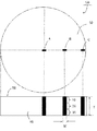
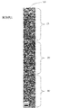
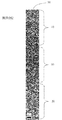
- FIG. 1 It is a schematic diagram which shows the cross-sectional area which carries out the EBSD measurement about the niobium sputtering target which concerns on one Embodiment of this invention. It is a crystal orientation distribution when the cross section of the target perpendicular to the sputtering surface is measured by EBSD at a position between the center and the outer periphery of the sputtering surface of the niobium sputtering target obtained in Example 1. It is a crystal orientation distribution when the cross section of the target perpendicular to the sputtered surface is measured by EBSD at a position intermediate between the center and the outer periphery of the sputtered surface of the niobium sputtering target obtained in Example 2.
- the present invention is not limited to each embodiment, and the components can be modified and embodied without departing from the gist thereof.
- various inventions can be formed by appropriately combining the plurality of components disclosed in each embodiment. For example, some components may be removed from all the components shown in the embodiments. Further, the components of different embodiments may be combined as appropriate.
- Niobium Sputtering Target composition
- all but unavoidable impurities are formed from niobium metal.
- the purity is 99.95% by mass or more. Impurities in the target deteriorate the reflection characteristics of the reflective film in the display device and also cause a decrease in the reliability of the interconnect of the quantum computer. Therefore, the one with as high purity as possible is preferable.
- the purity of 99.95% by mass or more is analyzed by glow discharge mass spectrometry (GDMS), and Na, Al, Si, K, Ti, Cr, Mn, Fe, Co, Ni, Cu, Zn, It means that the total value of Zr, Ta, Mo and W is 500 mass ppm or less.
- GDMS glow discharge mass spectrometry
- the shape of the niobium sputtering target according to the present invention is not particularly limited as long as it has a plate shape, and examples thereof include a flat plate shape such as a disk shape or a rectangular flat plate shape.
- the plate thickness of the niobium sputtering target is not limited, but can be, for example, 2 to 18 mm, and typically 3 to 10 mm.
- Niobium has the property that the ⁇ 111 ⁇ plane is oriented when strain is applied.
- the niobium sputtering target When a plate-shaped niobium sputtering target is manufactured through a rolling process, the niobium sputtering target generally has a region in which the ⁇ 111 ⁇ plane of crystal grains is oriented in the normal direction of the sputtered surface in the central portion in the thickness direction. (Hereinafter, also referred to as "band”) appears.
- the present invention is not intended to be limited, but this is considered to be due to the following reasons.
- pressure is applied from above and below in the thickness direction, so that the central portion in the thickness direction is strongly compressed from above and below. Further, the upper and lower parts in the thickness direction are prevented from being deformed by friction with the rolling roll, while the central part in the thickness direction is not in contact with the rolling roll and is not affected by the friction with the rolling roll, so that the strain is thick. Concentrate in the central part of the vertical direction. Therefore, in the niobium sputtering target, a band appears in the central portion in the thickness direction.
- the appearance of the band in the central portion in the thickness direction means that the crystal orientation changes in the central portion in the thickness direction of the sputtering target.
- the sputtering characteristics are different at the central portion in the thickness direction of the sputtering target, and the film thickness of the sputtering film changes.
- the film thickness uniformity of the sputtered film cannot be maintained throughout the target life.
- the band tends to develop especially at a position between the center of the sputtered surface and the outer circumference. That is, at a position intermediate between the center and the outer circumference of the sputtered surface, the difference between the maximum value and the minimum value of the area ratio between the upper portion, the central portion, and the lower portion becomes large.
- the cross section of the target perpendicular to the sputtering surface is formed on the sputtering surface at a position intermediate between the center and the outer periphery of the sputtering surface of the plate-shaped target.
- the sputter surface side is divided into three equal parts in the normal direction from the sputter surface side to the upper part, the central part, and the lower part, and the crystal orientation distributions of the upper part, the central part, and the lower part are measured by using the EBSD method.
- the rate of change represented by the above formula (2) is preferably 2.3 or less, and more preferably 2.1 or less.
- the lower limit of the rate of change represented by the above formula (2) is not particularly set and is most preferably 0, but is typically 0.1 or more, and more typically 1.0 or more. Is.
- the ⁇ 111 ⁇ area ratio of the central portion is 40% or less.
- the densest direction coincides with the normal direction of the sputtered surface, so that the film formation rate tends to be high. Therefore, by reducing the ⁇ 111 ⁇ area ratio of the central portion, the film thickness can be slowed down and the film thickness can be easily controlled.
- the ⁇ 111 ⁇ area ratio of the central portion is preferably 40% or less, more preferably 35% or less, and further preferably 33% or less.
- the lower limit of the ⁇ 111 ⁇ area ratio in the central portion is not particularly set, but is typically 5% or more, and more typically 10% or more.
- the ⁇ 111 ⁇ area ratio of the central portion is 60% or more.
- the film formation rate can be increased and the sputtering time can be shortened, thereby improving the production efficiency.
- the ⁇ 111 ⁇ area ratio of the central portion increases, the ⁇ 111 ⁇ area ratio of the upper and lower portions also increases, so that the entire sputtering target As a result, the film formation speed can be increased.
- the ⁇ 111 ⁇ area ratio in the middle is preferably 60% or more, more preferably 63% or more, and more preferably 66% or more. ..
- the upper limit of the ⁇ 111 ⁇ area ratio is not particularly limited, but is typically 80% or less.
- the crystal orientation distributions of the upper part, the central part, and the lower part are measured by using the EBSD method, and the measurement regions of the upper part, the central part, and the lower part are measured.
- the ⁇ 100 ⁇ area ratio is 30% or more, respectively.
- ⁇ 100 ⁇ area ratio total area of crystal grains whose ⁇ 100 ⁇ plane in the measurement region is oriented in the normal direction / total area of the measurement region ... Equation (3)
- Niobium which has a body-centered cubic structure, has an atomic close-packed direction of ⁇ 111>.
- the angle of the densest direction with respect to the normal direction of the sputtering surface becomes large (wide angle), so that niobium atoms radiate from the sputtering target during sputtering. Is kicked out. For this reason, the number of places where the film is partially thickened in the film formed by sputtering is reduced, and in-plane uniformity of a good film thickness can be obtained.
- the ⁇ 100 ⁇ area ratios of the upper part, the central part, and the lower part are preferably 30% or more, and preferably 32% or more, respectively.
- a cross section 40 perpendicular to the sputtering surface 50 is cut out through the center A of the sputtering surface 50 and polished with polishing paper (equivalent to # 2000 (JIS R 6253: 2006)). Then, it is buffed with a polyplastic solution to give a mirror surface, and then treated with a mixed solution of hydrofluoric acid, nitric acid, and hydrochloric acid.
- the center A is 165 mm from the outermost circumference to the center
- the outer circumference C is 15 mm from the outermost circumference to the center
- the middle B is 90 mm from the outermost circumference to the center.
- the measurement area is a total width of 1 mm, 0.5 mm in the outer peripheral direction and 0.5 mm in the central direction, centered on the intermediate B.
- a total width of 1 mm, 0.5 mm in each of the outer peripheral directions facing the center A, is set as the measurement area, and 0.5 mm in the outer peripheral direction and the center direction with the outer circumference C as the center.
- the measurement area may be a total width of 1 mm, which is 0.5 mm.
- an acceleration voltage of 15 kv, an irradiation current of 3.6 nA, a magnification of 20 times, and an inclination of 70 ° can be set.
- the thickness T of the niobium sputtering target 100 is divided into three equal parts from the sputtering surface 50 side to the upper portion 10, the central portion 20, and the lower portion 30 in the normal direction of the sputtering surface 50, and the upper portion 10 and the central portion.
- the ⁇ 111 ⁇ area ratio and the ⁇ 100 ⁇ area ratio are obtained according to the above-mentioned equations (1) and (3).
- the crystal grains whose ⁇ 111 ⁇ plane is oriented in the normal direction of the sputtered surface include crystal grains whose orientation deviation with respect to the normal direction of the sputtered surface of the ⁇ 111 ⁇ plane is within 15 °. ..
- the crystal grains whose ⁇ 100 ⁇ plane is oriented in the normal direction of the sputtered surface include crystal grains whose orientation deviation with respect to the normal direction of the sputtered surface of the ⁇ 100 ⁇ plane is within 15 °.
- the shape of the niobium sputtering target 100 is illustrated as a disk shape, but when the shape of the niobium sputtering target is a flat plate shape such as a rectangular flat plate shape, the shape of the niobium sputtering target 100 is the center of the sputtered surface as in the disc shape.
- the cross section of the target perpendicular to the sputtered surface at a position intermediate with the outer circumference may be measured by EBSD.
- the average crystal grain size of the upper part, the central part, and the lower part at a position intermediate between the center and the outer circumference of the sputtered surface is 30 to 100 ⁇ m, respectively. ..
- the grain size of the crystal grains in the sputtering target affects the mechanical properties such as the strength of the target, the uniformity of the structure, the film formation rate, and also affects the degree of abnormal discharge and particle generation, so it is appropriate. It is effective to control to.
- the particle size is within the above range over the entire thickness direction of the target, the fluctuation of the crystal particle size that appears on the surface one by one due to the erosion of sputtering is small even with the progress of sputtering, and throughout the target life. Stable sputtering characteristics can be achieved.
- the average crystal grain size of the upper part, the central part, and the lower part is preferably 100 ⁇ m or less, more preferably 80 ⁇ m or less, and further preferably 70 ⁇ m or less.
- the average crystal grain size of the upper part, the central part, and the lower part is preferably 30 ⁇ m or more, more preferably 40 ⁇ m or more, and further preferably 50 ⁇ m or more.
- the average crystal grain size of the upper part, the central part, and the lower part can be measured by the EBSD method in the same manner as when measuring the ⁇ 111 ⁇ area ratio and the ⁇ 100 ⁇ area ratio. Specifically, the number of crystal grains contained in the area of each of the upper, central, and lower measurement regions is calculated by the EBSD method, and the average area per grain existing in the measurement region is obtained. The circle equivalent diameter is defined as the average crystal grain size.
- the fact that the average crystal grain size of the upper part, the central part, and the lower part is within the range of the above rate of change means that the average crystal grain size of the upper part, the central part, and the lower part does not change significantly. Contributes to improving the film thickness uniformity through the process.
- the rate of change represented by the above formula (4) is preferably 1.0 or less, more preferably 0.5 or less, and even more preferably 0.2 or less.
- the lower limit of the rate of change represented by the above formula (4) is not particularly set, and is most preferably 0, but typically 0.01 or more.
- the temperature of the heat treatment is preferably 900 ° C. or lower, more preferably 850 ° C. or lower, and even more preferably 800 ° C. or lower, from the viewpoint of preventing excessive growth of crystal grains.
- the number of forgings can be appropriately selected for adjusting the forged structure.
- the billet is further cut into two to expose the texture formed inside the forged body to the cut surface, making it difficult for the influence of the texture to be passed on to the next rolling step. be able to.
- Dividing the billet into two is useful for suppressing the ⁇ 111 ⁇ plane of the crystal grain from being oriented in the normal direction of the sputter plane, especially in the central portion in the thickness direction.
- the rolling reduction ratio for each pass is preferably 18% or less, preferably 15% or less. Is more preferable, and 12% or less is further preferable. From the viewpoint of production efficiency, the reduction rate for each pass is typically 2% or more, and more typically 4% or more. At this time, the number of rolling passes is, for example, 11 times or more.
- the number of rolling passes is preferably 11 or more, and more preferably 15 or more, from the viewpoint of relatively increasing the proportion of crystal grains whose ⁇ 100 ⁇ plane is oriented in the normal direction. It is preferable, and more preferably 18 times or more. From the viewpoint of production efficiency, the number of rolling passes is preferably 40 or less, more preferably 30 or less, and even more preferably 25 or less.
- the rolling direction in which the forged product is rolled is set to the rolled plane for each pass. It is preferable to rotate 75 to 105 ° in parallel, and more preferably 85 to 95 °. By rotating the rolling direction by a predetermined angle for each pass, the generation of bands can be suppressed.
- the rolling may be performed several times while appropriately changing the rolling direction in order to adjust the shape of the rolled plate.
- the total rolling ratio is preferably adjusted to be 75% or more, and more preferably 80% or more, from the viewpoint of obtaining uniform and fine crystal grains.
- heat treatment may be performed during rolling, it is recommended that heat treatment be performed after final rolling (preferably 4 hours or more) without performing heat treatment during rolling.
- the temperature of the heat treatment is not particularly limited, but from the viewpoint of obtaining a recrystallized structure, 700 ° C. or higher is preferable, 750 ° C. or higher is more preferable, and 800 ° C. or higher is further preferable.
- the temperature of the heat treatment is preferably 900 ° C. or lower, more preferably 870 ° C. or lower, and even more preferably 850 ° C. or lower, from the viewpoint of preventing excessive growth of crystal grains.
- the texture formed by rolling or heat treatment obtains the desired texture orientation by grasping which surface is preferentially oriented by the EBSD method and feeding back the result to the conditions of rolling or heat treatment. be able to.
- the rolling may be repeated within the range of the number of passes and the rolling reduction described in the first manufacturing method, except that the rolling direction for rolling the forged body is constant.
- the region where the ⁇ 111 ⁇ plane of the crystal grain is oriented in the normal direction of the sputter plane can be expanded in the entire thickness direction of the target.
- the process after rolling is the same as that of the first manufacturing method.
- the reduction rate and the total reduction rate for each pass in the rolling process are higher than those in the first production method, so that the ⁇ 111 ⁇ plane of the crystal grains is further in the normal direction of the sputtered plane. It is also possible to extend the oriented region over the entire thickness direction of the target.
- Example 1 A niobium raw material having a purity of 99.95% by mass was melted with an electron beam and cast into an ingot having a length of 600 mm and a diameter of 245 mm ⁇ . Next, this ingot was cold-tightened and forged to have a diameter of 150 mm ⁇ , and then cut to a required length to obtain a billet. Next, heat treatment is performed at a temperature of 1000 ° C., primary forging is performed again in the cold, primary heat treatment is performed at 800 ° C., then secondary forging is performed in a columnar shape in the cold, the forged billet is divided into two, and again at 800 ° C. Secondary heat treatment was performed.
- the forged billet was cold-rolled.
- the rolling step was repeated 20 times in total while rotating the rolling direction by 90 ° in parallel with the rolling surface for each pass (rolling ratio: 11%).
- the total reduction rate was 89%.
- it was heat treated at 800 ° C.
- the obtained target material having a thickness of 8 mm ⁇ diameter of 400 mm ⁇ was subjected to finish machining to prepare a niobium sputtering target having a thickness of 6.35 mm ⁇ diameter of 322 mm ⁇ .
- EBSD measurement Crystal orientation distribution
- the obtained niobium sputtering target was measured by EBSD using an EBSD device (example: JSM-7001FTTLS type field emission electron microscope / crystal orientation analyzer OIM6.0-CCD / BS) according to the procedure described above, and the sputtered surface was subjected to EBSD measurement.
- Crystal orientation distributions of the upper part, the central part, and the lower part were obtained at a position intermediate between the center and the outer periphery (FIG. 2).
- the measurement conditions of the EBSD device were set to an accelerating voltage of 15 kv, an irradiation current of 3.6 nA, a magnification of 20 times, and an inclination of 70 °.
- Table 1 The results are shown in Table 1.
- Example 2 A square forged billet was prepared at 800 ° C. in the final heat treatment without dividing after forging into a square shape using the same method as in Example 1 up to the primary heat treatment. Next, the forged billet was cold rolled. In the rolling step, rolling was repeated for 19 passes (rolling ratio of 1 pass: 11%) in one direction without changing the rolling direction. The total reduction rate was 89%. After rolling, heat treatment was performed at 800 ° C. Next, the obtained square target material having a thickness of 9 mm, a width of 220 mm and a length of 480 mm was subjected to finish machining to prepare a niobium sputtering target having a thickness of 7 mm and a diameter of 180 mm ⁇ .
- the obtained niobium sputtering target was subjected to EBSD measurement using the same method as in Example 1, and the crystal orientation distributions of the upper part, the central part, and the lower part at a position intermediate between the center and the outer circumference of the sputtering surface were obtained. Obtained (Fig. 3). Then, the same evaluation as in Example 1 was performed. Further, EBSD measurement was also performed at the center and the outer circumference of the sputtered surface in the same manner as in Example 1 to obtain crystal orientation distributions at the upper part, the central part, and the lower part. The results are shown in Table 1.
- the obtained niobium sputtering target was subjected to EBSD measurement using the same method as in Example 1, and the crystal orientation distributions of the upper part, the central part, and the lower part at a position intermediate between the center and the outer circumference of the sputtering surface were obtained. Obtained (Fig. 4). Then, the same evaluation as in Example 1 was performed. Further, EBSD measurement was also performed at the center and the outer circumference of the sputtered surface in the same manner as in Example 1 to obtain crystal orientation distributions at the upper part, the central part, and the lower part. The results are shown in Table 1.
- the obtained niobium sputtering target was subjected to EBSD measurement using the same method as in Example 1, and the crystal orientation distributions of the upper part, the central part, and the lower part at a position intermediate between the center and the outer circumference of the sputtering surface were obtained. Obtained. Then, the same evaluation as in Example 1 was performed. Further, EBSD measurement was also performed at the center and the outer circumference of the sputtered surface in the same manner as in Example 1 to obtain crystal orientation distributions at the upper part, the central part, and the lower part. The results are shown in Table 1.
- the niobium sputtering target according to the present embodiment can form a thin film having excellent film thickness uniformity throughout the target life by setting the tissue orientation in a predetermined state. Therefore, it is useful as a niobium sputtering target used for forming a thin film of an antireflection film in a display device.
Landscapes
- Chemical & Material Sciences (AREA)
- Engineering & Computer Science (AREA)
- Materials Engineering (AREA)
- Mechanical Engineering (AREA)
- Metallurgy (AREA)
- Organic Chemistry (AREA)
- Chemical Kinetics & Catalysis (AREA)
- Physics & Mathematics (AREA)
- Plasma & Fusion (AREA)
- Analytical Chemistry (AREA)
- Physical Vapour Deposition (AREA)
- Air Conditioning Control Device (AREA)
Abstract
Description
板状のターゲットのスパッタ面の中心と外周との中間の位置において、前記スパッタ面に対して垂直な前記ターゲットの断面を前記スパッタ面の法線方向に前記スパッタ面側から上部、中央部、及び下部に三等分して、その上部、中央部、及び下部の結晶方位分布をEBSD法を用いて測定し、前記上部、中央部、及び下部のそれぞれの測定領域について下記式(1)に従って{111}面積率を求めた場合に、当該上部、中央部、及び下部の{111}面積率の下記式(2)に示される変化率が2.5以下である、ニオブスパッタリングターゲット。
{111}面積率=測定領域における{111}面が前記法線方向に配向している結晶粒の面積の合計/測定領域の全体の面積・・・式(1)
変化率=[最大値-最小値]/最小値・・・式(2)
[2]
前記中央部の{111}面積率が、40%以下である、[1]に記載のニオブスパッタリングターゲット。
[3]
前記中央部の{111}面積率が、60%以上である、[1]に記載のニオブスパッタリングターゲット。
[4]
前記上部、中央部、及び下部の結晶方位分布をEBSD法を用いて測定し、前記上部、中央部、及び下部のそれぞれの測定領域について、下記式(3)に従って{100}面積率を求めた場合に、{100}面積率が、それぞれ30%以上である、[1]~[3]のいずれか一項に記載のニオブスパッタリングターゲット。
{100}面積率=測定領域における{100}面が前記法線方向に配向している結晶粒の面積の合計/測定領域の全体の面積・・・式(3)
[5]
前記上部、中央部、及び下部の平均結晶粒径がそれぞれ30~100μmである、[1]~[4]のいずれか一項に記載のニオブスパッタリングターゲット。
[6]
前記上部、中央部、及び下部の平均結晶粒径について、下記式(4)に示される変化率が1.0以下である、[1]~[5]のいずれか一項に記載のニオブスパッタリングターゲット。
変化率=[最大値-最小値]/最小値・・・式(4)
(組成)
本発明に係るニオブスパッタリングターゲットの一実施形態においては、不可避不純物以外はニオブ金属から形成される。また、本発明に係るニオブスパッタリングターゲットの一実施形態においては、純度が99.95質量%以上であることが望ましい。ターゲット中の不純物は、ディスプレイ装置における反射膜の反射特性を劣化させるほか、量子コンピューターのインターコネクトの信頼性を低下させる要因になる。そのため、できるだけ高純度のものが好ましい。ここで、純度99.95質量%以上とは、グロー放電質量分析法(GDMS)にて分析し、Na、Al、Si、K、Ti、Cr、Mn、Fe、Co、Ni、Cu、Zn、Zr、Ta、Mo、Wの合計値が500質量ppm以下であることを意味する。
本発明に係るニオブスパッタリングターゲットの形状としては、板状であれば特に制限されないが、例えば円板状や矩形平板状等の平板状が挙げられる。ニオブスパッタリングターゲットの板厚としては、限定的ではないが、例えば2~18mmとすることができ、典型的には3~10mmとすることができる。
ニオブには、歪みを加えると{111}面が配向する性質がある。板状のニオブスパッタリングターゲットが圧延工程を経て製造される場合、ニオブスパッタリングターゲットには、一般に、厚さ方向の中央部に、結晶粒の{111}面がスパッタ面の法線方向に配向した領域(以下、「バンド」ともいう。)が現れる。
{111}面積率=測定領域における{111}面が前記法線方向に配向している結晶粒の面積の合計/測定領域の全体の面積・・・式(1)
変化率=[最大値-最小値]/最小値・・・式(2)
本発明に係るニオブスパッタリングターゲットの一実施形態においては、前記中央部の{111}面積率が、40%以下である。スパッタ面の法線方向に対して{111}面が配向している場合、最密方向がスパッタ面の法線方向と一致するため、成膜速度が速くなる傾向にある。そこで、前記中央部の{111}面積率を小さくすることにより、成膜速度を遅くして膜厚を制御し易くすることができる。上述した式(2)に示される変化率が小さいニオブスパッタリングターゲットにおいては、前記中央部の{111}面積率が小さくなると、前記上部及び下部の{111}面積率も小さくなるので、スパッタリングターゲット全体として成膜速度を遅くすることができる。膜厚制御性の観点からは、前記中央部の{111}面積率は、40%以下であることが好ましく、35%以下であることがより好ましく、33%以下であることが更に好ましい。なお、前記中央部の{111}面積率は、下限値は特に設定されないが、典型的には5%以上であり、より典型的には10%以上である。
成膜の生産効率を高めるという観点からは、上記中間の{111}面積率が、60%以上であることが好ましく、63%以上であることがより好ましく、66%以上であることがより好ましい。なお、上記{111}面積率の上限値は特にないが、典型的には80%以下である。
本発明に係るニオブスパッタリングターゲットの一実施形態においては、前記上部、中央部、及び下部の結晶方位分布をEBSD法を用いて測定し、前記上部、中央部、及び下部のそれぞれの測定領域について、下記式(3)に従って{100}面積率を求めた場合に、{100}面積率が、それぞれ30%以上である。
{100}面積率=測定領域における{100}面が前記法線方向に配向している結晶粒の面積の合計/測定領域の全体の面積・・・式(3)
EBSD法を用いた{111}面積率及び{100}面積率の求め方について、図1を参照しながら以下に説明する。まず、板状のニオブスパッタリングターゲット100について、スパッタ面50の中心Aを通り、スパッタ面50に対して垂直な断面40を切り出して、研磨紙(#2000相当(JIS R 6253:2006))で磨き、さらにポリプラ液を使用してバフ研磨して鏡面に仕上げ、その後、フッ酸、硝酸、塩酸の混合液で処理する。
本明細書においては、{111}面がスパッタ面の法線方向に配向している結晶粒には、{111}面のスパッタ面の法線方向に対する方位ずれが15°以内の結晶粒を含む。また、{100}面がスパッタ面の法線方向に配向している結晶粒には、{100}面のスパッタ面の法線方向に対する方位ずれが15°以内の結晶粒を含む。
なお、ここでは、ニオブスパッタリングターゲット100の形状が円板状を例示したが、ニオブスパッタリングターゲットの形状が矩形平板状等の平板状である場合には、円板状と同様にスパッタ面の中心と外周との中間の位置において、そのスパッタ面に対して垂直なターゲットの断面をEBSD測定すればよい。
本発明に係るニオブスパッタリングターゲットの一実施形態においては、スパッタ面の中心と外周との中間の位置における、前記上部、中央部、及び下部の平均結晶粒径がそれぞれ30~100μmであることが好ましい。スパッタリングターゲット内の結晶粒の粒径は、ターゲットの強度等の機械的特性、組織の均一性、成膜速度に影響を及ぼし、更には異常放電とパーティクル発生の程度にも影響を及ぼすため、適切に制御することが有効である。本実施形態によれば、ターゲットの厚み方向全体にわたって粒径が上記範囲内であることで、スパッタリングのエロージョンによって表面に逐一現れる結晶粒径の変動がスパッタリングの進行に伴っても小さく、ターゲットライフを通して安定したスパッタリング特性を達成できる。
前記上部、中央部、及び下部の平均結晶粒径については、{111}面積率及び{100}面積率を測定するときと同様に、EBSD法で測定可能である。具体的には、EBSD法によって前記上部、中央部、及び下部のそれぞれの測定領域の面積中に含まれる結晶粒の数を算出し、測定領域内に存在する1粒当たりの平均面積を求め、その円相当径を平均結晶粒径とする。
また、本発明に係るニオブスパッタリングターゲットの一実施形態においては、前記上部、中央部、及び下部の平均結晶粒径について、下記式(4)に示される変化率が1.0以下であることが好ましい。
変化率=[最大値-最小値]/最小値・・・式(4)
前記上部、中央部、及び下部の平均結晶粒径が、上記変化率の範囲内であることは、上部、中央部、及び下部の平均結晶粒径が大きく変化しないことを意味するので、ターゲットライフを通した膜厚均一性を向上することに寄与する。
上記式(4)に示される変化率は、1.0以下であることが好ましく、0.5以下であることがより好ましく、0.2以下であることが更に好ましい。なお、上記式(4)で示される変化率に下限値は特に設定されず、0であることが最も好ましいが、典型的には0.01以上である。
(第一製造方法)
最初に、結晶粒の{111}面がスパッタ面の法線方向に配向するのを抑制することで{111}面積の変化率が小さく制御されたニオブスパッタリングターゲットを製造する方法を説明する。まず、ニオブを溶解し、これを鋳造してインゴットを作製した後、このインゴットを鍛造する。その後、インゴットを締め鍛造してビレットとし、これを適当なサイズに切断した後、熱処理を行う。その後、鍛造と熱処理を2度繰り返す。また、熱処理の温度は特に限定されないが、鍛造組織の調整の観点から、700℃以上が好ましく、720℃以上がより好ましく、750℃以上が更に好ましい。ただし、上記熱処理の温度は、結晶粒の過度な成長を防止する観点から、900℃以下が好ましく、850℃以下がより好ましく、800℃以下が更に好ましい。なお、鍛造回数は、鍛造組織の調整のために適宜選択することができる。
次に、結晶粒の{111}面がスパッタ面の法線方向に配向した領域をターゲットの厚み方向全体に広げることで{111}面積の変化率が小さく制御されたニオブスパッタリングターゲットを製造する方法について説明する。まず、鍛造工程の終了までは第一製造方法と同様に実施する。ただし、すべての鍛造工程の終了後、ビレットを分割しないことが好ましい。ビレットを分割しないことで、結晶粒の{111}面がスパッタ面の法線方向に配向しやすくなるからである。次に、圧延工程では、鍛造体を圧延する圧延方向を一定にするという以外は、第一製造方法で説明したパス回数と圧下率の範囲内で圧延を繰り返せばよい。当該圧延工程により、結晶粒の{111}面がスパッタ面の法線方向に配向した領域をターゲットの厚み方向全体に広げることができる。圧延後の工程は、第一製造方法と同様である。但し、第二製造方法においては、圧延工程における1パスごとの圧下率及びトータル圧下率は第一製造方法よりも高くすることで、更に結晶粒の{111}面がスパッタ面の法線方向に配向した領域をターゲットの厚み方向全体に広げることも可能である。
純度99.95質量%のニオブ原料を電子ビーム溶解し、鋳造して長さ600mm×直径245mmφのインゴットとした。次に、このインゴットを冷間で締め鍛造し、直径150mmφとした後に必要長さで切断し、ビレットを得た。次に、1000℃の温度で熱処理し、再び冷間で一次鍛造し、800℃で一次熱処理し、次いで冷間で円柱状に二次鍛造を行い、鍛造ビレットを2分割し、再度800℃で二次熱処理した。
(結晶方位分布)
得られたニオブスパッタリングターゲットについて、EBSD装置(例示:JSM-7001FTTLS型 電界放出電子顕微鏡/結晶方位解析装置 OIM6.0-CCD/BS)を用いて、先述した手順でEBSD測定を行い、スパッタ面の中心と外周との中間の位置における、前記上部、中央部、及び下部の結晶方位分布を得た(図2)。EBSD装置の測定条件は、加速電圧15kv、照射電流3.6nA、倍率20倍、傾斜70°に設定した。
上記EBSD測定により、スパッタ面の中心と外周との中間の位置における前記上部、中央部、及び下部のそれぞれの測定領域における平均結晶粒径を求め、その変化率=[最大値-最小値]/最小値を算出した。結果については、表1に示す。
一次熱処理までを実施例1と同様の方法を用いて角状に鍛造し、その後分割を行わず、最終熱処理800℃で角状鍛造ビレットを作製した。次に、鍛造ビレットを冷間圧延した。圧延工程は、圧延方向を変えることなく一方向に19パス(1パスの圧下率:11%)だけ圧延を繰り返した。トータルの圧下率は、89%であった。圧延後、800℃で熱処理した。次に、得られた厚さ9mm×幅220mm×長さ480mmの角状ターゲット素材に対して仕上げ機械加工を行って、厚さ7mm×直径180mmφのニオブスパッタリングターゲットを作製した。
一次熱処理までを実施例1と同様の方法を用いて角状に鍛造し、その後分割を行わず、最終熱処理800℃でビレットを作製した。次に、鍛造ビレットを冷間圧延した。圧延工程は、圧延方向を1パス(圧下率:11%)ごとに圧延面に平行に90°回転させながら、計22回繰り返した。トータルの圧下率は、89%であった。圧延後、800℃で熱処理した。次に、得られた厚さ9mm、400mm角の角状ターゲット素材に対して仕上げ機械加工を行って、厚さ7mm×直径180mmφのニオブスパッタリングターゲットを作製した。
一次熱処理までを実施例1と同様の方法を用いて円柱状に鍛造し、その後分割を行わず、最終熱処理800℃でビレットを作製した。次に、鍛造ビレットを冷間圧延した。圧延工程は、圧延方向を1パス(圧下率:11%)ごとに90°回転させながら、計20回繰り返した。トータルの圧下率は、86%であった。圧延後、800℃で熱処理した。次に、得られた厚さ8mm×直径370mmφのターゲット素材に対して仕上げ機械加工を行って、厚さ6.35mm×直径322mmφのニオブスパッタリングターゲットを作製した。

20 中央部
30 下部
40 断面
50 スパッタ面
100 ニオブスパッタリングターゲット
A 中心
B 中間
C 外周
T 厚さ
W 幅
Claims (6)
- 板状のターゲットのスパッタ面の中心と外周との中間の位置において、前記スパッタ面に対して垂直な前記ターゲットの断面を前記スパッタ面の法線方向に前記スパッタ面側から上部、中央部、及び下部に三等分して、その上部、中央部、及び下部の結晶方位分布をEBSD法を用いて測定し、前記上部、中央部、及び下部のそれぞれの測定領域について下記式(1)に従って{111}面積率を求めた場合に、当該上部、中央部、及び下部の{111}面積率の下記式(2)に示される変化率が2.5以下である、ニオブスパッタリングターゲット。
{111}面積率=測定領域における{111}面が前記法線方向に配向している結晶粒の面積の合計/測定領域の全体の面積・・・式(1)
変化率=[最大値-最小値]/最小値・・・式(2) - 前記中央部の{111}面積率が、40%以下である、請求項1に記載のニオブスパッタリングターゲット。
- 前記中央部の{111}面積率が、60%以上である、請求項1に記載のニオブスパッタリングターゲット。
- 前記上部、中央部、及び下部の結晶方位分布をEBSD法を用いて測定し、前記上部、中央部、及び下部のそれぞれの測定領域について、下記式(3)に従って{100}面積率を求めた場合に、{100}面積率が、それぞれ30%以上である、請求項1~3のいずれか一項に記載のニオブスパッタリングターゲット。
{100}面積率=測定領域における{100}面が前記法線方向に配向している結晶粒の面積の合計/測定領域の全体の面積・・・式(3) - 前記上部、中央部、及び下部の平均結晶粒径がそれぞれ30~100μmである、請求項1~4のいずれか一項に記載のニオブスパッタリングターゲット。
- 前記上部、中央部、及び下部の平均結晶粒径について、下記式(4)に示される変化率が1.0以下である、請求項1~5のいずれか一項に記載のニオブスパッタリングターゲット。
変化率=[最大値-最小値]/最小値・・・式(4)
Priority Applications (6)
| Application Number | Priority Date | Filing Date | Title |
|---|---|---|---|
| JP2021508147A JP7076632B2 (ja) | 2019-03-26 | 2020-01-28 | ニオブスパッタリングターゲット |
| US17/439,123 US12020916B2 (en) | 2019-03-26 | 2020-01-28 | Niobium sputtering target |
| KR1020217032232A KR102704843B1 (ko) | 2019-03-26 | 2020-01-28 | 니오븀 스퍼터링 타깃 |
| CN202080021234.8A CN113574203A (zh) | 2019-03-26 | 2020-01-28 | 铌溅射靶 |
| EP20779665.7A EP3951004A4 (en) | 2019-03-26 | 2020-01-28 | NIOBIUM SPRAYINGTARGET |
| SG11202110358SA SG11202110358SA (en) | 2019-03-26 | 2020-01-28 | Niobium sputtering target |
Applications Claiming Priority (2)
| Application Number | Priority Date | Filing Date | Title |
|---|---|---|---|
| JP2019058996 | 2019-03-26 | ||
| JP2019-058996 | 2019-03-26 |
Publications (1)
| Publication Number | Publication Date |
|---|---|
| WO2020195121A1 true WO2020195121A1 (ja) | 2020-10-01 |
Family
ID=72609905
Family Applications (1)
| Application Number | Title | Priority Date | Filing Date |
|---|---|---|---|
| PCT/JP2020/003024 Ceased WO2020195121A1 (ja) | 2019-03-26 | 2020-01-28 | ニオブスパッタリングターゲット |
Country Status (8)
| Country | Link |
|---|---|
| US (1) | US12020916B2 (ja) |
| EP (1) | EP3951004A4 (ja) |
| JP (1) | JP7076632B2 (ja) |
| KR (1) | KR102704843B1 (ja) |
| CN (1) | CN113574203A (ja) |
| SG (1) | SG11202110358SA (ja) |
| TW (1) | TWI754220B (ja) |
| WO (1) | WO2020195121A1 (ja) |
Cited By (1)
| Publication number | Priority date | Publication date | Assignee | Title |
|---|---|---|---|---|
| WO2023224084A1 (ja) | 2022-05-19 | 2023-11-23 | 東ソー株式会社 | 金属スパッタリングターゲット及びその製造方法、並びに、金属材料及びその製造方法 |
Citations (3)
| Publication number | Priority date | Publication date | Assignee | Title |
|---|---|---|---|---|
| JP2004511651A (ja) * | 2000-05-22 | 2004-04-15 | キャボット コーポレイション | 高純度ニオブおよびそれを含む製品、ならびにその製造方法 |
| JP2014194072A (ja) | 2013-02-26 | 2014-10-09 | Mitsubishi Materials Corp | 酸化ニオブスパッタリングターゲット、その製造方法及び酸化ニオブ膜 |
| JP2018519413A (ja) * | 2015-04-10 | 2018-07-19 | トーソー エスエムディー,インク. | タンタルスパッターターゲットの製造方法及びこれにより製造されたスパッターターゲット |
Family Cites Families (7)
| Publication number | Priority date | Publication date | Assignee | Title |
|---|---|---|---|---|
| CN1257998C (zh) * | 2001-01-11 | 2006-05-31 | 卡伯特公司 | 钽和铌的坯料及其制造方法 |
| EP1366203B1 (en) | 2001-02-20 | 2006-09-13 | H. C. Starck, Inc. | Refractory metal plates with uniform texture and methods of making the same |
| US7067197B2 (en) | 2003-01-07 | 2006-06-27 | Cabot Corporation | Powder metallurgy sputtering targets and methods of producing same |
| CN101660130B (zh) | 2009-09-29 | 2011-06-01 | 西部金属材料股份有限公司 | 一种制备铌溅射靶材的方法 |
| CN103009000B (zh) * | 2012-12-18 | 2015-05-27 | 宁夏东方钽业股份有限公司 | 一种铌靶材及其制备方法 |
| JP5837214B2 (ja) * | 2013-03-27 | 2015-12-24 | Jx日鉱日石金属株式会社 | ニオブスパッタリングターゲット |
| WO2015157421A1 (en) | 2014-04-11 | 2015-10-15 | H.C. Starck Inc. | High purity refractory metal sputtering targets which have a uniform random texture manufactured by hot isostatic pressing high purity refractory metal powders |
-
2020
- 2020-01-28 JP JP2021508147A patent/JP7076632B2/ja active Active
- 2020-01-28 WO PCT/JP2020/003024 patent/WO2020195121A1/ja not_active Ceased
- 2020-01-28 EP EP20779665.7A patent/EP3951004A4/en active Pending
- 2020-01-28 US US17/439,123 patent/US12020916B2/en active Active
- 2020-01-28 SG SG11202110358SA patent/SG11202110358SA/en unknown
- 2020-01-28 KR KR1020217032232A patent/KR102704843B1/ko active Active
- 2020-01-28 CN CN202080021234.8A patent/CN113574203A/zh active Pending
- 2020-02-13 TW TW109104564A patent/TWI754220B/zh active
Patent Citations (3)
| Publication number | Priority date | Publication date | Assignee | Title |
|---|---|---|---|---|
| JP2004511651A (ja) * | 2000-05-22 | 2004-04-15 | キャボット コーポレイション | 高純度ニオブおよびそれを含む製品、ならびにその製造方法 |
| JP2014194072A (ja) | 2013-02-26 | 2014-10-09 | Mitsubishi Materials Corp | 酸化ニオブスパッタリングターゲット、その製造方法及び酸化ニオブ膜 |
| JP2018519413A (ja) * | 2015-04-10 | 2018-07-19 | トーソー エスエムディー,インク. | タンタルスパッターターゲットの製造方法及びこれにより製造されたスパッターターゲット |
Non-Patent Citations (1)
| Title |
|---|
| See also references of EP3951004A4 |
Cited By (2)
| Publication number | Priority date | Publication date | Assignee | Title |
|---|---|---|---|---|
| WO2023224084A1 (ja) | 2022-05-19 | 2023-11-23 | 東ソー株式会社 | 金属スパッタリングターゲット及びその製造方法、並びに、金属材料及びその製造方法 |
| KR20250011611A (ko) | 2022-05-19 | 2025-01-21 | 도소 가부시키가이샤 | 금속 스퍼터링 타깃 및 그 제조 방법, 그리고, 금속 재료 및 그 제조 방법 |
Also Published As
| Publication number | Publication date |
|---|---|
| EP3951004A4 (en) | 2022-12-14 |
| JPWO2020195121A1 (ja) | 2020-10-01 |
| JP7076632B2 (ja) | 2022-05-27 |
| TWI754220B (zh) | 2022-02-01 |
| US12020916B2 (en) | 2024-06-25 |
| TW202035727A (zh) | 2020-10-01 |
| KR20210134759A (ko) | 2021-11-10 |
| KR102704843B1 (ko) | 2024-09-10 |
| EP3951004A1 (en) | 2022-02-09 |
| SG11202110358SA (en) | 2021-10-28 |
| CN113574203A (zh) | 2021-10-29 |
| US20220157583A1 (en) | 2022-05-19 |
Similar Documents
| Publication | Publication Date | Title |
|---|---|---|
| CN100334252C (zh) | 钽溅射靶及其制造方法 | |
| US10658163B2 (en) | Tantalum sputtering target, and production method therefor | |
| JP7076632B2 (ja) | ニオブスパッタリングターゲット | |
| US20200240005A1 (en) | Titanium Sputtering Target, Production Method Therefor, And Method For Producing Titanium-Containing Thin Film | |
| JP6293928B2 (ja) | タンタルスパッタリングターゲット及びその製造方法 | |
| TWI665325B (zh) | Tantalum sputtering target | |
| JP2706635B2 (ja) | スパッタリング用高純度チタンターゲット及びその製造方法 | |
| TW202540463A (zh) | 具有改善的性能及可預測性之鉭濺射靶及其製造方法 | |
| JP5477790B2 (ja) | タンタルスパッタリングターゲット及びその製造方法 |
Legal Events
| Date | Code | Title | Description |
|---|---|---|---|
| 121 | Ep: the epo has been informed by wipo that ep was designated in this application |
Ref document number: 20779665 Country of ref document: EP Kind code of ref document: A1 |
|
| ENP | Entry into the national phase |
Ref document number: 2021508147 Country of ref document: JP Kind code of ref document: A |
|
| NENP | Non-entry into the national phase |
Ref country code: DE |
|
| ENP | Entry into the national phase |
Ref document number: 20217032232 Country of ref document: KR Kind code of ref document: A |
|
| ENP | Entry into the national phase |
Ref document number: 2020779665 Country of ref document: EP Effective date: 20211026 |