WO2020194932A1 - 表示装置 - Google Patents
表示装置 Download PDFInfo
- Publication number
- WO2020194932A1 WO2020194932A1 PCT/JP2019/049828 JP2019049828W WO2020194932A1 WO 2020194932 A1 WO2020194932 A1 WO 2020194932A1 JP 2019049828 W JP2019049828 W JP 2019049828W WO 2020194932 A1 WO2020194932 A1 WO 2020194932A1
- Authority
- WO
- WIPO (PCT)
- Prior art keywords
- capacitor
- light emitting
- display device
- capacity
- thin film
- Prior art date
- Legal status (The legal status is an assumption and is not a legal conclusion. Google has not performed a legal analysis and makes no representation as to the accuracy of the status listed.)
- Ceased
Links
Images



Classifications
-
- G—PHYSICS
- G09—EDUCATION; CRYPTOGRAPHY; DISPLAY; ADVERTISING; SEALS
- G09G—ARRANGEMENTS OR CIRCUITS FOR CONTROL OF INDICATING DEVICES USING STATIC MEANS TO PRESENT VARIABLE INFORMATION
- G09G3/00—Control arrangements or circuits, of interest only in connection with visual indicators other than cathode-ray tubes
- G09G3/20—Control arrangements or circuits, of interest only in connection with visual indicators other than cathode-ray tubes for presentation of an assembly of a number of characters, e.g. a page, by composing the assembly by combination of individual elements arranged in a matrix no fixed position being assigned to or needed to be assigned to the individual characters or partial characters
- G09G3/22—Control arrangements or circuits, of interest only in connection with visual indicators other than cathode-ray tubes for presentation of an assembly of a number of characters, e.g. a page, by composing the assembly by combination of individual elements arranged in a matrix no fixed position being assigned to or needed to be assigned to the individual characters or partial characters using controlled light sources
- G09G3/30—Control arrangements or circuits, of interest only in connection with visual indicators other than cathode-ray tubes for presentation of an assembly of a number of characters, e.g. a page, by composing the assembly by combination of individual elements arranged in a matrix no fixed position being assigned to or needed to be assigned to the individual characters or partial characters using controlled light sources using electroluminescent panels
- G09G3/32—Control arrangements or circuits, of interest only in connection with visual indicators other than cathode-ray tubes for presentation of an assembly of a number of characters, e.g. a page, by composing the assembly by combination of individual elements arranged in a matrix no fixed position being assigned to or needed to be assigned to the individual characters or partial characters using controlled light sources using electroluminescent panels semiconductive, e.g. using light-emitting diodes [LED]
- G09G3/3208—Control arrangements or circuits, of interest only in connection with visual indicators other than cathode-ray tubes for presentation of an assembly of a number of characters, e.g. a page, by composing the assembly by combination of individual elements arranged in a matrix no fixed position being assigned to or needed to be assigned to the individual characters or partial characters using controlled light sources using electroluminescent panels semiconductive, e.g. using light-emitting diodes [LED] organic, e.g. using organic light-emitting diodes [OLED]
- G09G3/3225—Control arrangements or circuits, of interest only in connection with visual indicators other than cathode-ray tubes for presentation of an assembly of a number of characters, e.g. a page, by composing the assembly by combination of individual elements arranged in a matrix no fixed position being assigned to or needed to be assigned to the individual characters or partial characters using controlled light sources using electroluminescent panels semiconductive, e.g. using light-emitting diodes [LED] organic, e.g. using organic light-emitting diodes [OLED] using an active matrix
- G09G3/3233—Control arrangements or circuits, of interest only in connection with visual indicators other than cathode-ray tubes for presentation of an assembly of a number of characters, e.g. a page, by composing the assembly by combination of individual elements arranged in a matrix no fixed position being assigned to or needed to be assigned to the individual characters or partial characters using controlled light sources using electroluminescent panels semiconductive, e.g. using light-emitting diodes [LED] organic, e.g. using organic light-emitting diodes [OLED] using an active matrix with pixel circuitry controlling the current through the light-emitting element
-
- G—PHYSICS
- G09—EDUCATION; CRYPTOGRAPHY; DISPLAY; ADVERTISING; SEALS
- G09F—DISPLAYING; ADVERTISING; SIGNS; LABELS OR NAME-PLATES; SEALS
- G09F9/00—Indicating arrangements for variable information in which the information is built-up on a support by selection or combination of individual elements
- G09F9/30—Indicating arrangements for variable information in which the information is built-up on a support by selection or combination of individual elements in which the desired character or characters are formed by combining individual elements
-
- G—PHYSICS
- G09—EDUCATION; CRYPTOGRAPHY; DISPLAY; ADVERTISING; SEALS
- G09F—DISPLAYING; ADVERTISING; SIGNS; LABELS OR NAME-PLATES; SEALS
- G09F9/00—Indicating arrangements for variable information in which the information is built-up on a support by selection or combination of individual elements
- G09F9/30—Indicating arrangements for variable information in which the information is built-up on a support by selection or combination of individual elements in which the desired character or characters are formed by combining individual elements
- G09F9/302—Indicating arrangements for variable information in which the information is built-up on a support by selection or combination of individual elements in which the desired character or characters are formed by combining individual elements characterised by the form or geometrical disposition of the individual elements
-
- G—PHYSICS
- G09—EDUCATION; CRYPTOGRAPHY; DISPLAY; ADVERTISING; SEALS
- G09G—ARRANGEMENTS OR CIRCUITS FOR CONTROL OF INDICATING DEVICES USING STATIC MEANS TO PRESENT VARIABLE INFORMATION
- G09G3/00—Control arrangements or circuits, of interest only in connection with visual indicators other than cathode-ray tubes
- G09G3/20—Control arrangements or circuits, of interest only in connection with visual indicators other than cathode-ray tubes for presentation of an assembly of a number of characters, e.g. a page, by composing the assembly by combination of individual elements arranged in a matrix no fixed position being assigned to or needed to be assigned to the individual characters or partial characters
- G09G3/22—Control arrangements or circuits, of interest only in connection with visual indicators other than cathode-ray tubes for presentation of an assembly of a number of characters, e.g. a page, by composing the assembly by combination of individual elements arranged in a matrix no fixed position being assigned to or needed to be assigned to the individual characters or partial characters using controlled light sources
- G09G3/30—Control arrangements or circuits, of interest only in connection with visual indicators other than cathode-ray tubes for presentation of an assembly of a number of characters, e.g. a page, by composing the assembly by combination of individual elements arranged in a matrix no fixed position being assigned to or needed to be assigned to the individual characters or partial characters using controlled light sources using electroluminescent panels
- G09G3/32—Control arrangements or circuits, of interest only in connection with visual indicators other than cathode-ray tubes for presentation of an assembly of a number of characters, e.g. a page, by composing the assembly by combination of individual elements arranged in a matrix no fixed position being assigned to or needed to be assigned to the individual characters or partial characters using controlled light sources using electroluminescent panels semiconductive, e.g. using light-emitting diodes [LED]
- G09G3/3208—Control arrangements or circuits, of interest only in connection with visual indicators other than cathode-ray tubes for presentation of an assembly of a number of characters, e.g. a page, by composing the assembly by combination of individual elements arranged in a matrix no fixed position being assigned to or needed to be assigned to the individual characters or partial characters using controlled light sources using electroluminescent panels semiconductive, e.g. using light-emitting diodes [LED] organic, e.g. using organic light-emitting diodes [OLED]
-
- H—ELECTRICITY
- H05—ELECTRIC TECHNIQUES NOT OTHERWISE PROVIDED FOR
- H05B—ELECTRIC HEATING; ELECTRIC LIGHT SOURCES NOT OTHERWISE PROVIDED FOR; CIRCUIT ARRANGEMENTS FOR ELECTRIC LIGHT SOURCES, IN GENERAL
- H05B33/00—Electroluminescent light sources
- H05B33/12—Light sources with substantially two-dimensional [2D] radiating surfaces
-
- H—ELECTRICITY
- H10—SEMICONDUCTOR DEVICES; ELECTRIC SOLID-STATE DEVICES NOT OTHERWISE PROVIDED FOR
- H10K—ORGANIC ELECTRIC SOLID-STATE DEVICES
- H10K59/00—Integrated devices, or assemblies of multiple devices, comprising at least one organic light-emitting element covered by group H10K50/00
- H10K59/10—OLED displays
- H10K59/12—Active-matrix OLED [AMOLED] displays
- H10K59/121—Active-matrix OLED [AMOLED] displays characterised by the geometry or disposition of pixel elements
- H10K59/1216—Active-matrix OLED [AMOLED] displays characterised by the geometry or disposition of pixel elements the pixel elements being capacitors
-
- H—ELECTRICITY
- H10—SEMICONDUCTOR DEVICES; ELECTRIC SOLID-STATE DEVICES NOT OTHERWISE PROVIDED FOR
- H10K—ORGANIC ELECTRIC SOLID-STATE DEVICES
- H10K59/00—Integrated devices, or assemblies of multiple devices, comprising at least one organic light-emitting element covered by group H10K50/00
- H10K59/30—Devices specially adapted for multicolour light emission
- H10K59/35—Devices specially adapted for multicolour light emission comprising red-green-blue [RGB] subpixels
- H10K59/353—Devices specially adapted for multicolour light emission comprising red-green-blue [RGB] subpixels characterised by the geometrical arrangement of the RGB subpixels
-
- G—PHYSICS
- G09—EDUCATION; CRYPTOGRAPHY; DISPLAY; ADVERTISING; SEALS
- G09G—ARRANGEMENTS OR CIRCUITS FOR CONTROL OF INDICATING DEVICES USING STATIC MEANS TO PRESENT VARIABLE INFORMATION
- G09G2300/00—Aspects of the constitution of display devices
- G09G2300/04—Structural and physical details of display devices
- G09G2300/0421—Structural details of the set of electrodes
- G09G2300/0426—Layout of electrodes and connections
-
- G—PHYSICS
- G09—EDUCATION; CRYPTOGRAPHY; DISPLAY; ADVERTISING; SEALS
- G09G—ARRANGEMENTS OR CIRCUITS FOR CONTROL OF INDICATING DEVICES USING STATIC MEANS TO PRESENT VARIABLE INFORMATION
- G09G2300/00—Aspects of the constitution of display devices
- G09G2300/08—Active matrix structure, i.e. with use of active elements, inclusive of non-linear two terminal elements, in the pixels together with light emitting or modulating elements
- G09G2300/0809—Several active elements per pixel in active matrix panels
- G09G2300/0842—Several active elements per pixel in active matrix panels forming a memory circuit, e.g. a dynamic memory with one capacitor
- G09G2300/0861—Several active elements per pixel in active matrix panels forming a memory circuit, e.g. a dynamic memory with one capacitor with additional control of the display period without amending the charge stored in a pixel memory, e.g. by means of additional select electrodes
-
- G—PHYSICS
- G09—EDUCATION; CRYPTOGRAPHY; DISPLAY; ADVERTISING; SEALS
- G09G—ARRANGEMENTS OR CIRCUITS FOR CONTROL OF INDICATING DEVICES USING STATIC MEANS TO PRESENT VARIABLE INFORMATION
- G09G2310/00—Command of the display device
- G09G2310/02—Addressing, scanning or driving the display screen or processing steps related thereto
- G09G2310/0243—Details of the generation of driving signals
- G09G2310/0251—Precharge or discharge of pixel before applying new pixel voltage
-
- G—PHYSICS
- G09—EDUCATION; CRYPTOGRAPHY; DISPLAY; ADVERTISING; SEALS
- G09G—ARRANGEMENTS OR CIRCUITS FOR CONTROL OF INDICATING DEVICES USING STATIC MEANS TO PRESENT VARIABLE INFORMATION
- G09G2310/00—Command of the display device
- G09G2310/02—Addressing, scanning or driving the display screen or processing steps related thereto
- G09G2310/0262—The addressing of the pixel, in a display other than an active matrix LCD, involving the control of two or more scan electrodes or two or more data electrodes, e.g. pixel voltage dependent on signals of two data electrodes
-
- G—PHYSICS
- G09—EDUCATION; CRYPTOGRAPHY; DISPLAY; ADVERTISING; SEALS
- G09G—ARRANGEMENTS OR CIRCUITS FOR CONTROL OF INDICATING DEVICES USING STATIC MEANS TO PRESENT VARIABLE INFORMATION
- G09G2310/00—Command of the display device
- G09G2310/08—Details of timing specific for flat panels, other than clock recovery
Definitions
- the present invention relates to a display device.
- the organic electroluminescence display device emits light from the light emitting layer in multiple gradations by passing a current corresponding to the input image signal, thereby displaying an image (Patent Document 1).
- the current is controlled by the thin film transistor.
- An object of the present invention is to eliminate the difference in current control due to the thin film transistor.
- the display device includes a plurality of light emitting elements provided for each of a plurality of emission color sub-pixels constituting each of the plurality of pixels, a drive circuit for driving each of the plurality of light emitting elements, and a drive circuit for driving each of the plurality of light emitting elements.
- the plurality of light emitting elements include a first light emitting element corresponding to one of the plurality of light emitting colors and a second light emitting element corresponding to the other one of the plurality of light emitting colors.
- the first light emitting element has a larger light emitting region than the second light emitting element, and the drive circuit includes high-potential wiring and low-potential wiring for passing a current through the corresponding one of the plurality of light emitting elements.
- a current switching element that switches the flow and cutoff of the current, a thin film that is connected in series with the current switching element to control the amount of the current, and a signal switching element that switches the input and cut of a video signal to the gate of the thin film.
- a holding capacitor interposed between one of the source and drain of the thin film and the gate, an element capacitor composed of a corresponding one of the plurality of light emitting elements, and the one and the height of the source and drain.
- the drive circuit for driving the first light emitting element includes a first element capacitor as the element capacitor and the additional capacitor, including an additional capacitor interposed between the potential wiring and the low potential wiring.
- the drive circuit for driving the second light emitting element includes a second element capacitor as the element capacitor and a second additional capacitor as the additional capacitor.
- the capacity of the first element capacitor is larger than the capacity of the second element capacitor, and the capacity of the first additional capacitor is smaller than the capacity of the second additional capacitor.
- the first light emitting element has a larger capacity of the first element capacitor because the light emitting region is larger than that of the second light emitting element, but the capacity of the first addition capacitor is smaller. As a result, it is possible to eliminate the difference in current control between the first light emitting element and the second light emitting element.
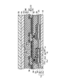
- FIG. 5 is a sectional view taken along line VV of the display device shown in FIG.
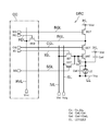
- VI-VI line sectional view of the display device shown in FIG. It is a figure which shows the detail of a drive circuit.
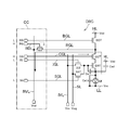
- It is a figure which shows the operation in the period 1 of FIG. It is a figure which shows the operation in the period 2 of FIG.
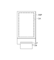
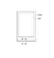
- FIG. 1 is a plan view of the display device according to the embodiment. Since the display device is actually used by being bent, FIG. 1 is a developed view before the display device is bent.
- FIG. 2 is a schematic view showing a usage state of the display device.
- FIG. 3 is a schematic view of a cross section taken along line III-III of the display device shown in FIG.
- the display device is, for example, an organic electroluminescence display device.
- the display device includes a display DSP.
- a spacer SP is arranged inside the bend to prevent the display DSP from bending too much.
- the display DSP is flexible and is folded outside the display area DA on which the image is displayed.
- the display DSP is equipped with an integrated circuit chip CP for driving an element for displaying an image.
- a flexible printed circuit board FP is connected to the display DSP outside the display area DA.
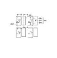
- FIG. 4 is a diagram showing a part of the display area shown in FIG.
- a full-color one-pixel PX is formed by combining a plurality of sub-pixel SPXs (sub-pixels) whose emission colors are red R, green G, and blue B, and a full-color image is produced by the plurality of pixel PXs. Is displayed. Since the sensitivity of the human eye is lower than that of blue B, the sub-pixel SPX of blue B is the largest.
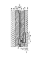
- FIG. 5 is a sectional view taken along line VV of the display device shown in FIG. Specifically, it is sectional drawing of the sub-pixel SPX whose emission color is blue B.
- the substrate 10 is made of polyimide. However, other resin materials may be used as long as the base material has sufficient flexibility to form a sheet display or a flexible display.
- a barrier inorganic film 12 (undercoat layer) is laminated on the substrate 10.
- the barrier inorganic film 12 has a three-layer laminated structure of a silicon oxide film 12a, a silicon nitride film 12b, and a silicon oxide film 12c.
- the silicon nitride film 12b of the middle layer is a blocking film of moisture and impurities from the outside, and the silicon oxide film 12c of the uppermost layer is a silicon nitride film.
- Each of them is provided as a block film for preventing the hydrogen atom contained in 12b from diffusing on the semiconductor layer 16 side of the thin film transistor DRT, but the structure is not particularly limited, and further lamination may be performed, or simply. It may be a layer or a two-layer laminate.
- the functional film 14 may be formed according to the location where the thin film transistor DRT is formed.
- the functional film 14 suppresses changes in the characteristics of the thin film transistor DRT due to intrusion of light from the back surface of the channel, or is formed of a conductive material to give a predetermined potential to give the thin film transistor DRT a back gate effect. Can be done.
- the functional film 14 is formed in an island shape according to the location where the thin film transistor DRT is formed, and then the silicon nitride film 12b and the silicon oxide film 12c are laminated to form a barrier inorganic film.
- the functional film 14 is formed so as to be enclosed in the film 12, but the present invention is not limited to this, and the functional film 14 may be first formed on the substrate 10 and then the barrier inorganic film 12 may be formed.
- a thin film transistor DRT is formed on the barrier inorganic film 12. Taking a polysilicon thin film transistor as an example, only the Nch transistor is shown here, but the Pch transistor may be formed at the same time.
- the semiconductor layer 16 of the thin film transistor DRT adopts a structure in which a low-concentration impurity region is provided between a channel region and a source / drain region.
- a silicon oxide film is used here as the gate insulating film 18.
- the gate electrode 20 is a part of the first wiring layer W1 formed of MoW.
- the first wiring layer W1 has a first holding capacitance line CL1 in addition to the gate electrode 20.
- a part of the holding capacitor Cs is formed between the first holding capacitance line CL1 and the semiconductor layer 16 (source / drain region) via the gate insulating film 18.
- An interlayer insulating film 22 (silicon oxide film and silicon nitride film) is laminated on the gate electrode 20.
- a second wiring layer W2 including a portion serving as a source / drain electrode 24 is formed on the interlayer insulating film 22.
- a three-layer laminated structure of Ti, Al and Ti is adopted.
- the first holding capacitance line CL1 (a part of the first wiring layer W1) and the second holding capacitance line CL2 (a part of the second wiring layer W2) pass through the interlayer insulating film 22, and the other holding capacitors Cs. Part is formed.
- a passivation film 26 is formed on the interlayer insulating film 22 so as to cover the second wiring layer W2 (source / drain electrode 24).
- a flattening organic film 28 is provided on the passivation film 26. Since the flattening organic film 28 is superior in surface flatness as compared with an inorganic insulating material formed by CVD (Chemical Vapor Deposition) or the like, a resin such as photosensitive acrylic is used.
- the flattened organic film 28 and the passivation film 26 are removed at the pixel contact portion 30, and an indium tin oxide (ITO) film 32 is formed on the flattened organic film 28 and the passivation film 26.
- the indium tin oxide film 32 includes a first transparent conductive film 32a and a second transparent conductive film 32b separated from each other.
- the second wiring layer W2 whose surfaces are exposed by removing the flattening organic film 28 and the passivation film 26 is covered with the first transparent conductive film 32a.
- a silicon nitride film 34 is provided on the flattening organic film 28 so as to cover the first transparent conductive film 32a.
- the silicon nitride film 34 has an opening in the pixel contact portion 30, and the pixel electrode 36 is laminated so as to conduct electricity to the source / drain electrode 24 through the opening.
- the pixel electrode 36 is formed as a reflective electrode and has a three-layer laminated structure of an indium zinc oxide film, an Ag film, and an indium zinc oxide film.
- an indium tin oxide film may be used instead of the indium zinc oxide film.
- the pixel electrode 36 extends laterally from the pixel contact portion 30 and reaches above the thin film transistor DRT.
- the second transparent conductive film 32b is provided adjacent to the pixel contact portion 30 and below the pixel electrode 36 (further below the silicon nitride film 34).
- the second transparent conductive film 32b, the silicon nitride film 34, and the pixel electrode 36 overlap each other, whereby the first addition capacitor Cad1 is formed.
- the first addition capacitor Cad1 has a first counter electrode 46A facing the pixel electrode 36.
- a bank rib
- photosensitive acrylic or the like is used as in the flattened organic film 28. It is preferable that the insulating organic film 38 is opened so as to expose the surface of the pixel electrode 36 as a light emitting region, and the open end thereof has a gently tapered shape. If the open end has a steep shape, the coverage of the organic electroluminescence layer 40 formed on the open end is poor.
- the flattening organic film 28 and the insulating organic film 38 are in contact with each other through an opening provided in the silicon nitride film 34 between them. As a result, moisture and degassing desorbed from the flattening organic film 28 can be extracted through the insulating organic film 38 through heat treatment or the like after the formation of the insulating organic film 38.
- An organic electroluminescence layer 40 made of an organic material is laminated on the pixel electrode 36.
- the organic electroluminescence layer 40 may be a single layer, but may have a structure in which a hole transport layer, a light emitting layer, and an electron transport layer are laminated in this order from the pixel electrode 36 side. These layers may be formed by thin film deposition.
- a common electrode 42 is provided on the organic electroluminescence layer 40.
- the common electrode 42 is transparent.
- the Mg layer and the Ag layer are formed as a thin film to which the emitted light from the organic electroluminescence layer 40 is transmitted.
- the pixel electrode 36 serves as an anode and the common electrode 42 serves as a cathode.
- the first light emitting element LE1 is composed of a plurality of pixel electrodes 36, a common electrode 42, and an organic electroluminescence layer 40 interposed between the central portion of each of the plurality of pixel electrodes 36 and the common electrode 42.
- the first light emitting element LE1 constitutes the first element capacitor Cel1.
- a sealing layer 48 covering the first light emitting element LE1 is formed on the common electrode 42.
- the sealing layer 48 has one of the functions of preventing the invasion of moisture from the outside of the previously formed organic electroluminescence layer 40, and is required to have a high gas barrier property.
- the sealing layer 48 has a laminated structure of an organic film 50, a first inorganic film 52 sandwiching the organic film 50, and a second inorganic film 54 (for example, a silicon nitride film).
- a resin layer 56 and a polarizing plate 58 (for example, a circular polarizing plate) are laminated on the sealing layer 48.
- FIG. 6 is a sectional view taken along line VI-VI of the display device shown in FIG. More specifically, it is a cross-sectional view of a sub-pixel SPX whose emission colors are red R and green G.
- the second light emitting element LE2 constitutes the second element capacitor Cel2.
- the first light emitting element LE1 shown in FIG. 5 has a larger light emitting region than the second light emitting element LE2 shown in FIG. 6 (see FIG. 4). Specifically, the pixel electrode 36 of the first light emitting element LE1 is larger than the pixel electrode 36 of the second light emitting element LE2.
- the pixel electrode 36 which is the one electrode 36A of the first addition capacitor Cad1 shown in FIG. 5, is larger than the pixel electrode 36, which is the one electrode 36B of the second addition capacitor Cad2 shown in FIG.
- the second addition capacitor Cad2 has a second counter electrode 46B facing the pixel electrode 36 (one electrode 36B).
- the first counter electrode 46A (FIG. 5) included in the first addition capacitor Cad1 is smaller than the second counter electrode 46B (FIG. 6) included in the second addition capacitor Cad2.
- Other configurations are the same as those shown in FIG.
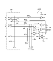
- FIG. 7 is a diagram showing details of the drive circuit.
- the plurality of light emitting elements LE includes a first light emitting element LE1 (FIG. 5) corresponding to one of the plurality of emission colors R, G, and B.
- the plurality of light emitting elements LE includes a second light emitting element LE2 (FIG. 6) corresponding to the other one of the plurality of emission colors R, G, and B.
- the display device has a plurality of light emitting elements LE provided in the sub-pixels SPX of the plurality of light emitting colors R, G, and B constituting each of the plurality of pixel PXs.
- the display device has a drive circuit DRC for driving each of the plurality of light emitting elements LE.
- the potential difference between the high-potential wiring HL and the low-potential wiring LL allows a current to flow through each of the plurality of light emitting elements LE.
- the flow and interruption of the current is switched by the current switching element BCT.
- a thin film transistor DRT is connected in series to the current switching element BCT to control the amount of current.
- the input and cutoff of the video signal Vsig to the gate of the thin film transistor DRT can be switched by the signal switching element SST.
- Holding capacitors Cs are interposed between one of the source and drain of the thin film transistor DRT and the gate.
- Each of the plurality of light emitting elements LE constitutes an element capacitor Cel.
- the element capacitor Cel is a capacitance attached between the anode (pixel electrode 36) and the cathode (common electrode 42) of the light emitting element LE.
- the drive circuit DRC for driving the first light emitting element LE1 shown in FIG. 5 includes the first element capacitor Cel1 as the element capacitor Cel.
- the drive circuit DRC for driving the second light emitting element LE2 shown in FIG. 6 includes the second element capacitor Cel2 as the element capacitor Cel.
- Each of the plurality of pixel electrodes 36 is shared as one electrode 36A and 36B of the element capacitor Cel and the addition capacitor Cad, respectively. On the other hand, since the electrode 36A is larger than the one electrode 36B, the capacitance of the first element capacitor Cel1 is larger than the capacitance of the second element capacitor Cel2.
- the drive circuit DRC includes an additional capacitor CAD interposed between one of the source and drain and one of the high potential wiring HL and the low potential wiring LL.
- the drive circuit DRC for driving the first light emitting element LE1 shown in FIG. 5 includes a first additional capacitor Cad1 as an additional capacitor Cad.
- the drive circuit DRC for driving the second light emitting element LE2 shown in FIG. 6 includes a second additional capacitor Cad2 as an additional capacitor Cad.
- the capacitance of the first addition capacitor Cad1 is smaller than the capacitance of the second addition capacitor Cad2.
- the total capacitance of the first element capacitor Cel1 and the capacitance of the first additional capacitor Cad1 is equal to the total capacitance of the second element capacitor Cel2 and the capacitance of the second additional capacitor Cad2.
- the first light emitting element LE1 shown in FIG. 5 has a larger capacitance of the first element capacitor Cel1 due to the larger light emitting region than the second light emitting element LE2 shown in FIG. 1
- the capacity of the additional capacitor Cad1 is small.
- Signals BG, CG, IG, and SG are output from the control circuit CC to the optical control line BGL, the correction control line CGL, the initialization control line IGL, and the write control line SGL, respectively.
- the drive circuit DRC is provided with a current switching element BCT, a correction transistor CCT, an initialization transistor IST, a signal switching element SST, and a thin film transistor DRT. At least one of these transistors may be shared between adjacent drive circuit DRCs. Retention capacitors Cs are provided between the gate and source of the thin film transistor DRT.
- the current switching element BCT, the correction transistor CCT, the initialization transistor IST, and the signal switching element SST function as switching elements for selecting conduction or non-conduction between two nodes.
- the thin film transistor DRT functions as a current control element that controls the current value flowing through the light emitting element LE according to the gate-source voltage.
- the transistor used may be an N-type transistor or a P-type transistor. When a P-type transistor is used, it is advisable to appropriately match the connection of the power supply potential and the holding capacitance.
- the anode of the light emitting element LE is connected to the high potential wiring HL of high potential (power supply voltage Vdd) via the current switching element BCT, the correction transistor CCT, and the thin film transistor DRT.
- the cathode is connected to the low potential wiring LL having a low potential (power supply voltage Vss).
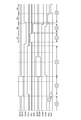
- FIG. 8 is a diagram showing a timing chart of the control circuit CC for driving the drive circuit DRC.
- the signals RG, BG, CG, and IG are input to the drive circuit DRC group arranged in two lines at the same time, and the two-digit numbers attached after the codes RG, BG, CG, and IG are respectively. Indicates the line number to which the signal of is input.
- the one-digit number added after the code SG indicates the line number to which the signal is input.
- Each section represented by the reference numerals G1 to G4 has one horizontal period, and although omitted thereafter, the same timing relationship continues until the last line. In FIG. 8, the periods 0 to 6 will be described in detail below.
- the light emitting element LE continues the light emitting state of the previous frame until the processing in a certain frame period is started (period 0).
- FIG. 9 is a diagram showing the operation in the period 1 of FIG. In this period, the signal BG becomes the L level, the signal CG becomes the H level, the signal RG becomes the H level, the current switching element BCT is turned off, and the correction transistor CCT is turned on. The signal RG becomes H level, and the reset transistor RST is turned on via the reset drive line RDL.
- One reset transistor RST is provided outside the display area DA, for example, in each row. The current from the power supply voltage Vdd is cut off by the current switching element BCT, and the light emitting of the light emitting element LE is stopped.
- the electric charge remaining on the anode side of the light emitting element LE is drawn out to the reset potential line RVL through the reset transistor RST via the reset control line RGL.
- the source of the thin film transistor DRT is fixed at the reset potential Vrst.
- the reset potential Vrst is set to a potential lower than the emission start voltage of the light emitting element LE with respect to the power supply voltage Vss.
- FIG. 10 is a diagram showing the operation in the period 2 of FIG. In this period, the signal IG becomes H level and the initialization transistor IST is turned on. As a result, the gate of the thin film transistor DRT is fixed to the initialization potential Vini via the initialization potential line IVL.
- the initialization potential Vini is set to a potential larger than the threshold value Vth of the thin film transistor DRT with respect to the reset potential Vrst. That is, by this operation, the thin film transistor DRT is turned on. However, since the current switching element BCT is off, no current flows through the thin film transistor DRT yet.
- FIG. 11 is a diagram showing the operation in the period 3 of FIG. In this period, the signal BG becomes the H level, the signal RG becomes the L level, the current switching element BCT turns on, and the reset transistor RST turns off. Since the thin film transistor DRT is turned on by the previous operation, a current is supplied to the thin film transistor DRT from the power supply voltage Vdd through the current switching element BCT and the correction transistor CCT.
- the source of the thin film transistor DRT is charged by the current supplied from the power supply voltage Vdd, and its potential rises.
- the thin film transistor DRT since the gate potential of the thin film transistor DRT is the initialization potential Vini, the thin film transistor DRT is turned off when the source potential of the thin film transistor DRT becomes (Vini-Vth), and the rise of the source potential stops.
- the threshold voltage Vth of the thin film transistor DRT varies depending on the drive circuit DRC
- the potential of the source of the thin film transistor DRT when the increase in potential is stopped differs depending on the drive circuit DRC. That is, by this operation, a voltage corresponding to the threshold voltage Vth of the thin film transistor DRT is acquired between the source and the gate in each drive circuit DRC.
- the operations from the source initialization (period 1) to the offset cancellation (period 3) of the thin film transistor DRT are performed in parallel for the drive circuit DRC group for two lines.
- FIG. 12 is a diagram showing the operation during the periods 4 and 5 of FIG. In this period, the signal CG becomes L level, the signal IG becomes L level, the signal SG becomes H level, the correction transistor CCT is turned off, the initialization transistor IST is turned off, and the signal switching element SST is turned on.
- the video signal Vsig is input to the gate of the thin film transistor DRT, and the gate potential of the thin film transistor DRT changes from the initialization potential Vini to the video signal Vsig. That is, the video signal Vsig is written to the gate of the thin film transistor DRT.
- the source potential of the thin film transistor DRT becomes a potential (Vini-Vth) corresponding to the value of the threshold voltage Vth. Therefore, a write of the same video signal Vsig, the gate-source voltage V GS of the TFT DRT becomes to reflect the variation in the threshold voltage Vth ⁇ Vsig- (Vini-Vth) ⁇ . That is, even if there is a variation in the threshold voltage Vth between the drive circuits DRC, it is possible to perform writing corrected accordingly.
- the first line is written, and in period 5, the second line is written.
- the even-numbered lines are written.
- the signal switching element SST is turned off at odd-numbered lines to enter a "waiting" state. Since the video signal line SL sharing the video signal Vsig is common to the drive circuits DRC of a plurality of lines belonging to the same column, the video signal writing operation is sequentially performed line by line.
- FIG. 13 is a diagram showing the operation in the period 6 of FIG. In this period, the signal CG becomes H level, the signal SG becomes L level, the correction transistor CCT is turned on, and the signal switching element SST is turned off. A current is supplied from the power supply voltage Vdd to the thin film transistor DRT through the current switching element BCT and the correction transistor CCT.
- the thin film transistor DRT causes a current corresponding to the gate-source voltage V GS set up to the previous step to flow through the light emitting element LE, and the light emitting element LE emits light with brightness corresponding to the current. Since the voltage between the anode and the cathode of the light emitting element LE at this time becomes a voltage corresponding to the current, the potential on the anode side rises, and the holding capacitor Cs holds the voltage between the gate and the source of the thin film transistor DRT. The gate potential of the thin film transistor DRT also rises due to the coupling of the holding capacitors Cs.
- the increase in the gate potential of the thin film transistor DRT is larger than the increase in the potential on the anode side. Slightly smaller. Since this value is known, the potential of the video signal Vsig may be determined so as to obtain a desired current value at the gate-source voltage of the final thin film transistor DRT.
- the present invention is not limited to the above-described embodiment, and various modifications are possible.
- the configurations described in the embodiments can be replaced with substantially the same configurations, configurations that exhibit the same effects, or configurations that can achieve the same objectives.
Landscapes
- Engineering & Computer Science (AREA)
- Physics & Mathematics (AREA)
- General Physics & Mathematics (AREA)
- Theoretical Computer Science (AREA)
- Computer Hardware Design (AREA)
- Geometry (AREA)
- Microelectronics & Electronic Packaging (AREA)
- Electroluminescent Light Sources (AREA)
- Control Of Indicators Other Than Cathode Ray Tubes (AREA)
- Control Of El Displays (AREA)
- Devices For Indicating Variable Information By Combining Individual Elements (AREA)
Abstract
駆動回路(DRC)は、保持キャパシタ(Cs)と、素子キャパシタ(Cel)と、ソース及びドレインの一方と高電位配線(HL)及び低電位配線(LL)の一方の間に介在する付加キャパシタ(Cad)と、を含む。第1発光素子(LE1)を駆動するための駆動回路(DRC)は、素子キャパシタ(Cel)としての第1素子キャパシタ(Cel1)と、付加キャパシタ(Cad)としての第1付加キャパシタ(Cad1)と、を含む。第2発光素子(LE2)を駆動するための駆動回路(DRC)は、素子キャパシタ(Cel)としての第2素子キャパシタ(Cel2)と、付加キャパシタ(Cad)としての第2付加キャパシタ(Cad2)と、を含む。第1素子キャパシタ(Cel1)の容量は、第2素子キャパシタ(Cel2)の容量よりも大きい。第1付加キャパシタ(Cad1)の容量は、第2付加キャパシタ(Cad2)の容量よりも小さい。
Description
本発明は、表示装置に関する。
有機エレクトロルミネセンス表示装置は、入力された画像信号に対応した電流を流すことで発光層を多階調で発光し、これにより画像を表示するようになっている(特許文献1)。電流は、薄膜トランジスタによって制御される。
薄膜トランジスタによる電流の制御には、電位の安定が重要である。そのために画素電極を一方の電極とする容量が形成されるが、発光色によって電極の大きさが異なるため、その容量は発光色ごとに異なる。容量の違いで、薄膜トランジスタによる電流制御に差が生じる。さらに、電流が流れない状態の黒表示ができないとコントラストが悪化する。
本発明は、薄膜トランジスタによる電流制御の差をなくすことを目的とする。
本発明に係る表示装置は、複数の画素のそれぞれを構成する複数の発光色の副画素にそれぞれ設けられた複数の発光素子と、前記複数の発光素子のそれぞれを駆動するための駆動回路と、を有し、前記複数の発光素子は、前記複数の発光色の1つに対応する第1発光素子と、前記複数の発光色の他の1つに対応する第2発光素子と、を含み、前記第1発光素子は、前記第2発光素子よりも、発光領域が大きく、前記駆動回路は、前記複数の発光素子の対応する1つに電流を流すための高電位配線及び低電位配線と、前記電流の流れ及び遮断を切り替える電流スイッチング素子と、前記電流スイッチング素子と直列に接続されて前記電流の量を制御する薄膜トランジスタと、前記薄膜トランジスタのゲートへの映像信号の入力及び遮断を切り替える信号スイッチング素子と、前記薄膜トランジスタのソース及びドレインの一方と前記ゲートとの間に介在する保持キャパシタと、前記複数の発光素子の対応する1つからなる素子キャパシタと、前記ソース及び前記ドレインの前記一方と前記高電位配線及び前記低電位配線の一方の間に介在する付加キャパシタと、を含み、前記第1発光素子を駆動するための前記駆動回路は、前記素子キャパシタとしての第1素子キャパシタと、前記付加キャパシタとしての第1付加キャパシタと、を含み、前記第2発光素子を駆動するための前記駆動回路は、前記素子キャパシタとしての第2素子キャパシタと、前記付加キャパシタとしての第2付加キャパシタと、を含み、前記第1素子キャパシタの容量は、前記第2素子キャパシタの容量よりも大きく、前記第1付加キャパシタの容量は、前記第2付加キャパシタの容量よりも小さいことを特徴とする。
本発明によれば、第1発光素子は、第2発光素子と比較して、発光領域が大きいことで第1素子キャパシタの容量が大きいが、第1付加キャパシタの容量が小さくなっている。これにより、第1発光素子及び第2発光素子の間で、電流制御の差をなくすことができる。
以下、本発明の実施形態について図面を参照して説明する。但し、本発明は、その要旨を逸脱しない範囲において様々な態様で実施することができ、以下に例示する実施形態の記載内容に限定して解釈されるものではない。
図面は、説明をより明確にするため、実際の態様に比べ、各部の幅、厚さ、形状等について模式的に表される場合があるが、あくまで一例であって、本発明の解釈を限定するものではない。本明細書と各図において、既出の図に関して説明したものと同様の機能を備えた要素には、同一の符号を付して、重複する説明を省略することがある。
さらに、本発明の詳細な説明において、ある構成物と他の構成物の位置関係を規定する際、「上に」「下に」とは、ある構成物の直上あるいは直下に位置する場合のみでなく、特に断りの無い限りは、間にさらに他の構成物を介在する場合を含むものとする。
図1は、実施形態に係る表示装置の平面図である。表示装置は、実際には、折り曲げて使用するので、図1は、表示装置を折り曲げる前の展開図である。図2は、表示装置の使用状態を示す概略図である。図3は、図2に示す表示装置のIII-III線断面の概略図である。
表示装置は、例えば、有機エレクトロルミネセンス表示装置である。表示装置は、ディスプレイDSPを含む。屈曲の内側にはスペーサSPが配置されて、ディスプレイDSPの曲がりすぎを防いでいる。ディスプレイDSPは、可撓性を有し、画像が表示される表示領域DAの外側で折り曲げられている。ディスプレイDSPには、画像を表示するための素子を駆動するための集積回路チップCPが搭載されている。ディスプレイDSPには、表示領域DAの外側で、フレキシブルプリント基板FPが接続されている。
図4は、図1に示す表示領域の一部を示す図である。表示領域DAでは、例えば、発光色が赤R、緑G及び青Bの複数からなる副画素SPX(サブピクセル)を組み合わせてフルカラーの1画素PXを形成し、複数の画素PXによってフルカラーの画像が表示される。人の目の感度は、青Bに対して低いため、青Bの副画素SPXが最も大きくなっている。
図5は、図1に示す表示装置のV-V線断面図である。詳しくは、発光色が青Bの副画素SPXの断面図である。基板10は、ポリイミドからなる。ただし、シートディスプレイ又はフレキシブルディスプレイを構成するために十分な可撓性を有する基材であれば他の樹脂材料を用いてもよい。
基板10上に、バリア無機膜12(アンダーコート層)が積層されている。バリア無機膜12は、シリコン酸化膜12a、シリコン窒化膜12b及びシリコン酸化膜12cの三層積層構造である。最下層のシリコン酸化膜12aは、基板10との密着性向上のため、中層のシリコン窒化膜12bは、外部からの水分及び不純物のブロック膜として、最上層のシリコン酸化膜12cは、シリコン窒化膜12b中に含有する水素原子が薄膜トランジスタDRTの半導体層16側に拡散しないようにするブロック膜として、それぞれ設けられるが、特にこの構造に限定するものではなく、さらに積層があってもよいし、単層あるいは二層積層であってもよい。
薄膜トランジスタDRTを形成する箇所に合わせて機能膜14を形成してもよい。機能膜14は、チャネル裏面からの光の侵入等による薄膜トランジスタDRTの特性の変化を抑制したり、導電材料で形成して所定の電位を与えることで、薄膜トランジスタDRTにバックゲート効果を与えたりすることができる。ここでは、シリコン酸化膜12aを形成した後、薄膜トランジスタDRTが形成される箇所に合わせて機能膜14を島状に形成し、その後シリコン窒化膜12b及びシリコン酸化膜12cを積層することで、バリア無機膜12に機能膜14を封入するように形成しているが、この限りではなく、基板10上にまず機能膜14を形成し、その後にバリア無機膜12を形成してもよい。
バリア無機膜12上に薄膜トランジスタDRTが形成されている。ポリシリコン薄膜トランジスタを例に挙げて、ここではNchトランジスタのみを示しているが、Pchトランジスタを同時に形成してもよい。薄膜トランジスタDRTの半導体層16は、チャネル領域とソース・ドレイン領域との間に、低濃度不純物領域を設けた構造を採る。ゲート絶縁膜18としてはここではシリコン酸化膜を用いる。ゲート電極20は、MoWから形成された第1配線層W1の一部である。第1配線層W1は、ゲート電極20に加え、第1保持容量線CL1を有する。第1保持容量線CL1と半導体層16(ソース・ドレイン領域)との間で、ゲート絶縁膜18を介して、保持キャパシタCsの一部が形成される。
ゲート電極20の上に、層間絶縁膜22(シリコン酸化膜及びシリコン窒化膜)が積層されている。層間絶縁膜22の上に、ソース・ドレイン電極24となる部分を含む第2配線層W2が形成されている。ここでは、Ti、Al及びTiの三層積層構造を採用する。層間絶縁膜22を介して、第1保持容量線CL1(第1配線層W1の一部)と第2保持容量線CL2(第2配線層W2の一部)とで、保持キャパシタCsの他の一部が形成される。
第2配線層W2(ソース・ドレイン電極24)を覆って、層間絶縁膜22の上にパッシベーション膜26が形成されている。パッシベーション膜26の上には平坦化有機膜28が設けられている。平坦化有機膜28は、CVD(Chemical Vapor Deposition)等により形成される無機絶縁材料に比べ、表面の平坦性に優れることから、感光性アクリル等の樹脂が用いられる。
平坦化有機膜28及びパッシベーション膜26は、画素コンタクト部30では除去されて、その上に酸化インジウムスズ(Indium Tin Oxide:ITO)膜32が形成されている。酸化インジウムスズ膜32は、相互に分離された第1透明導電膜32a及び第2透明導電膜32bを含む。平坦化有機膜28及びパッシベーション膜26の除去により表面が露出した第2配線層W2は、第1透明導電膜32aにて被覆される。第1透明導電膜32aを被覆するように、平坦化有機膜28の上にシリコン窒化膜34が設けられている。シリコン窒化膜34は、画素コンタクト部30に開口を有し、この開口を介してソース・ドレイン電極24に導通するように画素電極36が積層されている。画素電極36は、反射電極として形成され、酸化インジウム亜鉛膜、Ag膜、酸化インジウム亜鉛膜の三層積層構造になっている。ここで、酸化インジウム亜鉛膜に代わって酸化インジウムスズ膜を用いてもよい。画素電極36は、画素コンタクト部30から側方に拡がり、薄膜トランジスタDRTの上方に至る。
第2透明導電膜32bは、画素コンタクト部30に隣接して、画素電極36の下方(さらにシリコン窒化膜34の下方)に設けられている。第2透明導電膜32b、シリコン窒化膜34及び画素電極36は重なっており、これらによって第1付加キャパシタCad1が形成される。第1付加キャパシタCad1は、画素電極36に対向する第1対向電極46Aを有する。
平坦化有機膜28の上であって例えば画素コンタクト部30の上方に、バンク(リブ)と呼ばれて隣同士の画素領域の隔壁となる絶縁有機膜38が形成されている。絶縁有機膜38としては平坦化有機膜28と同じく感光性アクリル等が用いられる。絶縁有機膜38は、画素電極36の表面を発光領域として露出するように開口され、その開口端はなだらかなテーパー形状となるのが好ましい。開口端が急峻な形状になっていると、その上に形成される有機エレクトロルミネセンス層40のカバレッジ不良を生ずる。
平坦化有機膜28と絶縁有機膜38は、両者間にあるシリコン窒化膜34に設けた開口を通じて接触している。これにより、絶縁有機膜38の形成後の熱処理等を通じて、平坦化有機膜28から脱離する水分や脱ガスを、絶縁有機膜38を通じて引き抜くことができる。
画素電極36の上に、有機材料からなる有機エレクトロルミネセンス層40が積層されている。有機エレクトロルミネセンス層40は、単層であってもよいが、画素電極36側から順に、正孔輸送層、発光層及び電子輸送層が積層された構造であってもよい。これらの層は、蒸着によって形成してもよい。
有機エレクトロルミネセンス層40の上に、共通電極42が設けられている。ここでは、トップエミッション構造としているため、共通電極42は透明である。例えば、Mg層及びAg層を、有機エレクトロルミネセンス層40からの出射光が透過する程度の薄膜として形成する。前述の有機エレクトロルミネセンス層40の形成順序に従うと、画素電極36が陽極となり、共通電極42が陰極となる。複数の画素電極36と、共通電極42と、複数の画素電極36のそれぞれの中央部と共通電極42の間に介在する有機エレクトロルミネセンス層40とで第1発光素子LE1が構成される。第1発光素子LE1は、第1素子キャパシタCel1を構成する。
共通電極42の上に、第1発光素子LE1を覆う封止層48が形成されている。封止層48は、先に形成した有機エレクトロルミネセンス層40を、外部からの水分侵入を防止することを機能の一としており、高いガスバリア性が要求される。封止層48は、有機膜50及びこれを挟む第1無機膜52及び第2無機膜54(例えばシリコン窒化膜)の積層構造になっている。封止層48には、樹脂層56及び偏光板58(例えば円偏光板)が積層されている。
図6は、図1に示す表示装置のVI-VI線断面図である。詳しくは、発光色が赤R及び緑Gの副画素SPXの断面図である。第2発光素子LE2は、第2素子キャパシタCel2を構成する。図5に示す第1発光素子LE1が、図6に示す第2発光素子LE2よりも、発光領域が大きい(図4参照)。具体的には、第1発光素子LE1の画素電極36が、第2発光素子LE2の画素電極36よりも大きい。
図5に示す第1付加キャパシタCad1の一方電極36Aである画素電極36は、図6に示す第2付加キャパシタCad2の一方電極36Bである画素電極36よりも大きい。第2付加キャパシタCad2は、画素電極36(一方電極36B)に対向する第2対向電極46Bを有する。第1付加キャパシタCad1に含まれる第1対向電極46A(図5)は、第2付加キャパシタCad2に含まれる第2対向電極46B(図6)よりも小さい。その他の構成は、図5に示す内容と同じである。
図7は、駆動回路の詳細を示す図である。複数の発光素子LEは、複数の発光色R,G,Bの1つに対応する第1発光素子LE1(図5)を含む。複数の発光素子LEは、複数の発光色R,G,Bの他の1つに対応する第2発光素子LE2(図6)を含む。表示装置は、複数の画素PXのそれぞれを構成する複数の発光色R,G,Bの副画素SPXにそれぞれ設けられた複数の発光素子LEを有する。表示装置は、複数の発光素子LEのそれぞれを駆動するための駆動回路DRCを有する。
高電位配線HL及び低電位配線LLの電位差によって、複数の発光素子LEのそれぞれに電流を流すことができる。その電流の流れ及び遮断は、電流スイッチング素子BCTによって切り替えられる。電流スイッチング素子BCTには、薄膜トランジスタDRTが直列に接続されて電流の量を制御するようになっている。薄膜トランジスタDRTのゲートへの映像信号Vsigの入力及び遮断は、信号スイッチング素子SSTによって切り替えられるようになっている。薄膜トランジスタDRTのソース及びドレインの一方とゲートとの間に保持キャパシタCsが介在する。
複数の発光素子LEのそれぞれは素子キャパシタCelを構成する。素子キャパシタCelは、発光素子LEの陽極(画素電極36)及び陰極(共通電極42)の間に付く容量である。図5に示す第1発光素子LE1を駆動するための駆動回路DRCは、素子キャパシタCelとしての第1素子キャパシタCel1を含む。図6に示す第2発光素子LE2を駆動するための駆動回路DRCは、素子キャパシタCelとしての第2素子キャパシタCel2を含む。複数の画素電極36のそれぞれは、素子キャパシタCel及び付加キャパシタCadのそれぞれの一方電極36A,36Bとして共用される。一方電極36Aが一方電極36Bよりも大きいことから、第1素子キャパシタCel1の容量は、第2素子キャパシタCel2の容量よりも大きい。
駆動回路DRCは、ソース及びドレインの一方と高電位配線HL及び低電位配線LLの一方の間に介在する付加キャパシタCadを含む。図5に示す第1発光素子LE1を駆動するための駆動回路DRCは、付加キャパシタCadとしての第1付加キャパシタCad1を含む。図6に示す第2発光素子LE2を駆動するための駆動回路DRCは、付加キャパシタCadとしての第2付加キャパシタCad2を含む。
第1対向電極46Aが第2対向電極46Bよりも小さいことから、第1付加キャパシタCad1の容量は、第2付加キャパシタCad2の容量よりも小さい。第1素子キャパシタCel1の容量及び第1付加キャパシタCad1の容量の合計容量は、第2素子キャパシタCel2の容量及び第2付加キャパシタCad2の容量の合計容量に等しい。
本実施形態によれば、図5に示す第1発光素子LE1は、図6に示す第2発光素子LE2と比較して、発光領域が大きいことで第1素子キャパシタCel1の容量が大きいが、第1付加キャパシタCad1の容量が小さくなっている。これにより、第1発光素子LE1及び第2発光素子LE2の間で、電流制御の差をなくすことができる。
光制御線BGL、補正制御線CGL、初期化制御線IGL、書込制御線SGLには、制御回路CCから、それぞれ、信号BG,CG,IG,SGが出力される。駆動回路DRCには、電流スイッチング素子BCT、補正トランジスタCCT、初期化トランジスタIST、信号スイッチング素子SST、薄膜トランジスタDRTが設けられる。これらのトランジスタの少なくとも1つは、隣接する駆動回路DRC間で共有されても良い。薄膜トランジスタDRTのゲート・ソース間には保持キャパシタCsが設けられている。
電流スイッチング素子BCT、補正トランジスタCCT、初期化トランジスタIST、信号スイッチング素子SSTは、2ノード間の導通、非導通を選択するスイッチング素子として機能する。薄膜トランジスタDRTは、そのゲート・ソース間電圧に応じて、発光素子LEに流れる電流値を制御する電流制御素子として機能する。使用されるトランジスタは、N型トランジスタであってもよいし、P型トランジスタであってもよい。P型トランジスタを用いる場合は、適宜電源電位や保持容量の接続を適合させるとよい。
発光素子LEの陽極は、電流スイッチング素子BCT、補正トランジスタCCT、薄膜トランジスタDRTを介して、高電位(電源電圧Vdd)の高電位配線HLに接続される。陰極は、低電位(電源電圧Vss)の低電位配線LLに接続される。
図8は、駆動回路DRCを駆動するための制御回路CCのタイミングチャートを示す図である。本実施形態では、信号RG,BG,CG,IGは、それぞれ、2行に並ぶ駆動回路DRC群に同時に入力され、符号RG,BG,CG,IGの後ろに付けた2桁の数字は、それぞれの信号が入力される行番号を示す。符号SGの後ろに付けた1桁の数字は、その信号が入力される行番号を示す。符号G1~G4で示される各区間が1水平期間であり、以後省略するが最終行まで、同様のタイミング関係が継続する。図8中、期間0~6について、以下詳細に説明する。
[前フレームでの発光]
図8において、あるフレーム期間での処理が開始されるまでの間(期間0)では、発光素子LEは、前フレームの発光状態を継続している。
図8において、あるフレーム期間での処理が開始されるまでの間(期間0)では、発光素子LEは、前フレームの発光状態を継続している。
[薄膜トランジスタDRTのソース初期化]
図9は、図8の期間1での動作を示す図である。この期間ではまず信号BGがLレベル、信号CGがHレベル、信号RGがHレベルとなり、電流スイッチング素子BCTがオフし、補正トランジスタCCTがオンする。信号RGがHレベルとなり、リセット駆動線RDLを介してリセットトランジスタRSTがオンする。リセットトランジスタRSTは、表示領域DAの外側に、例えば各行に1つ設けられる。電源電圧Vddからの電流は電流スイッチング素子BCTによって遮断されて、発光素子LEの発光が停止する。発光素子LEの陽極側に残留していた電荷が、リセット制御線RGLを介して、リセットトランジスタRSTを通じて、リセット電位線RVLに引き抜かれる。これにより、薄膜トランジスタDRTのソースがリセット電位Vrstに固定される。リセット電位Vrstは、電源電圧Vssに対して、発光素子LEの発光開始電圧よりも低い電位に設定されている。
図9は、図8の期間1での動作を示す図である。この期間ではまず信号BGがLレベル、信号CGがHレベル、信号RGがHレベルとなり、電流スイッチング素子BCTがオフし、補正トランジスタCCTがオンする。信号RGがHレベルとなり、リセット駆動線RDLを介してリセットトランジスタRSTがオンする。リセットトランジスタRSTは、表示領域DAの外側に、例えば各行に1つ設けられる。電源電圧Vddからの電流は電流スイッチング素子BCTによって遮断されて、発光素子LEの発光が停止する。発光素子LEの陽極側に残留していた電荷が、リセット制御線RGLを介して、リセットトランジスタRSTを通じて、リセット電位線RVLに引き抜かれる。これにより、薄膜トランジスタDRTのソースがリセット電位Vrstに固定される。リセット電位Vrstは、電源電圧Vssに対して、発光素子LEの発光開始電圧よりも低い電位に設定されている。
[薄膜トランジスタDRTのゲート初期化]
図10は、図8の期間2での動作を示す図である。この期間では、信号IGがHレベルとなり、初期化トランジスタISTがオンする。これにより、初期化電位線IVLを介して薄膜トランジスタDRTのゲートが初期化電位Viniに固定される。初期化電位Viniは、リセット電位Vrstに対して薄膜トランジスタDRTのしきい値Vthよりも大きい電位に設定されている。つまり、この操作によって、薄膜トランジスタDRTはオン状態となる。ただし、電流スイッチング素子BCTがオフしているので、薄膜トランジスタDRTにはまだ電流は流れない。
図10は、図8の期間2での動作を示す図である。この期間では、信号IGがHレベルとなり、初期化トランジスタISTがオンする。これにより、初期化電位線IVLを介して薄膜トランジスタDRTのゲートが初期化電位Viniに固定される。初期化電位Viniは、リセット電位Vrstに対して薄膜トランジスタDRTのしきい値Vthよりも大きい電位に設定されている。つまり、この操作によって、薄膜トランジスタDRTはオン状態となる。ただし、電流スイッチング素子BCTがオフしているので、薄膜トランジスタDRTにはまだ電流は流れない。
[オフセットキャンセル]
図11は、図8の期間3での動作を示す図である。この期間では、信号BGがHレベル、信号RGがLレベルとなり、電流スイッチング素子BCTがオンし、リセットトランジスタRSTがオフする。薄膜トランジスタDRTは前動作によってオン状態であるから、電流スイッチング素子BCT、補正トランジスタCCTを通じて電源電圧Vddから薄膜トランジスタDRTに電流が供給される。
図11は、図8の期間3での動作を示す図である。この期間では、信号BGがHレベル、信号RGがLレベルとなり、電流スイッチング素子BCTがオンし、リセットトランジスタRSTがオフする。薄膜トランジスタDRTは前動作によってオン状態であるから、電流スイッチング素子BCT、補正トランジスタCCTを通じて電源電圧Vddから薄膜トランジスタDRTに電流が供給される。
この段階では、発光素子LEの陽極・陰極間の電圧は発光開始電圧を上回っていないので、電流が流れない。従って、電源電圧Vddから供給された電流によって、薄膜トランジスタDRTのソースが充電され、その電位が上昇する。このとき、薄膜トランジスタDRTのゲート電位は初期化電位Viniとなっているので、薄膜トランジスタDRTのソース電位が(Vini-Vth)となった段階で薄膜トランジスタDRTがオフし、ソース電位の上昇が停止する。
薄膜トランジスタDRTのしきい値電圧Vthは、駆動回路DRCによってばらつきがあるため、電位の上昇が停止したときの薄膜トランジスタDRTのソースの電位は駆動回路DRCによって異なる。つまり、本動作によって、各駆動回路DRCで薄膜トランジスタDRTのしきい値電圧Vthに相当する電圧が、ソース・ゲート間に取得される。
このとき、発光素子LEの陽極・陰極間には、{(Vini-Vth)-Vss}の電圧Vleが印加されているが、この電圧は依然発光開始電圧を上回っていないので、発光素子LEには電流が流れない。
なお、図8のタイミングチャートによると、薄膜トランジスタDRTのソース初期化(期間1)からオフセットキャンセル(期間3)までの動作は、2行分の駆動回路DRC群に対して並行して実施されているが、この限りではない。1行ごとに順次実施されても良いし、3行以上を並行して実施しても良い。
[映像信号書込み]
図12は、図8の期間4,5での動作を示す図である。この期間では、信号CGがLレベル、信号IGがLレベル、信号SGがHレベルとなり、補正トランジスタCCTがオフし、初期化トランジスタISTがオフし、信号スイッチング素子SSTがオンする。これにより、映像信号Vsigが薄膜トランジスタDRTのゲートに入力され、薄膜トランジスタDRTのゲート電位は初期化電位Viniから映像信号Vsigに変化する。つまり、映像信号Vsigが薄膜トランジスタDRTのゲートに書き込まれる。
図12は、図8の期間4,5での動作を示す図である。この期間では、信号CGがLレベル、信号IGがLレベル、信号SGがHレベルとなり、補正トランジスタCCTがオフし、初期化トランジスタISTがオフし、信号スイッチング素子SSTがオンする。これにより、映像信号Vsigが薄膜トランジスタDRTのゲートに入力され、薄膜トランジスタDRTのゲート電位は初期化電位Viniから映像信号Vsigに変化する。つまり、映像信号Vsigが薄膜トランジスタDRTのゲートに書き込まれる。
このとき、先のオフセットキャンセル(期間3)を通じて、薄膜トランジスタDRTのソース電位は、しきい値電圧Vthの値に応じた電位(Vini-Vth)となっている。そのため、同じ映像信号Vsigを書き込んでも、薄膜トランジスタDRTのゲート・ソース間電圧VGSは、しきい値電圧Vthのばらつきを反映して{Vsig-(Vini-Vth)}となる。つまり、駆動回路DRC間のしきい値電圧Vthにばらつきがあっても、それに対応して補正した書き込みが可能になる。
期間4では1行目の書き込みを行い、期間5では2行目の書き込みを行う。同様に、奇数行の書込みが終わった後に偶数行の書込みを行う。偶数行の書込み中は、奇数行では信号スイッチング素子SSTがオフして「待ち」状態になる。映像信号Vsigを共有する映像信号線SLは、同列に属する複数行の駆動回路DRCで共通であるから、映像信号書込み動作は、1行ごとに順次実施される。
[発光]
図13は、図8の期間6での動作を示す図である。この期間では、信号CGがHレベル、信号SGがLレベルとなり、補正トランジスタCCTがオンし、信号スイッチング素子SSTがオフする。電流スイッチング素子BCT、補正トランジスタCCTを通じて電源電圧Vddから薄膜トランジスタDRTに電流が供給される。
図13は、図8の期間6での動作を示す図である。この期間では、信号CGがHレベル、信号SGがLレベルとなり、補正トランジスタCCTがオンし、信号スイッチング素子SSTがオフする。電流スイッチング素子BCT、補正トランジスタCCTを通じて電源電圧Vddから薄膜トランジスタDRTに電流が供給される。
薄膜トランジスタDRTは、前段階までで設定されたゲート・ソース間電圧VGSに応じた電流を発光素子LEに流し、発光素子LEがその電流に応じた輝度で発光する。このときの発光素子LEの陽極・陰極間電圧は、その電流に応じた電圧となるため、陽極側の電位が上昇し、保持キャパシタCsによって薄膜トランジスタDRTのゲート・ソース間電圧が保持される。保持キャパシタCsのカップリングによって薄膜トランジスタDRTのゲート電位も上昇する。
実際には、薄膜トランジスタDRTのゲートに対しては、保持キャパシタCsのみならず付加キャパシタCadや、その他の寄生容量が付いているため、陽極側の電位上昇よりも、薄膜トランジスタDRTのゲート電位の上昇はわずかに小さくなる。この値は既知であるから、最終的な薄膜トランジスタDRTのゲート・ソース間電圧において所望の電流値となるように、映像信号Vsigの電位を決定すれば良い。
以上により、一連の動作が完了する。当該動作を1行目から最終行まで完了すると、1フレーム期間内での1画面の表示となる。以後、当該動作を繰り返して映像の表示が行われる。
本発明は、上述した実施形態に限定されるものではなく種々の変形が可能である。例えば、実施形態で説明した構成は、実質的に同一の構成、同一の作用効果を奏する構成又は同一の目的を達成することができる構成で置き換えることができる。
Claims (5)
- 複数の画素のそれぞれを構成する複数の発光色の副画素にそれぞれ設けられた複数の発光素子と、
前記複数の発光素子のそれぞれを駆動するための駆動回路と、
を有し、
前記複数の発光素子は、前記複数の発光色の1つに対応する第1発光素子と、前記複数の発光色の他の1つに対応する第2発光素子と、を含み、
前記第1発光素子は、前記第2発光素子よりも、発光領域が大きく、
前記駆動回路は、
前記複数の発光素子の対応する1つに電流を流すための高電位配線及び低電位配線と、
前記電流の流れ及び遮断を切り替える電流スイッチング素子と、
前記電流スイッチング素子と直列に接続されて前記電流の量を制御する薄膜トランジスタと、
前記薄膜トランジスタのゲートへの映像信号の入力及び遮断を切り替える信号スイッチング素子と、
前記薄膜トランジスタのソース及びドレインの一方と前記ゲートとの間に介在する保持キャパシタと、
前記複数の発光素子の対応する1つからなる素子キャパシタと、
前記ソース及び前記ドレインの前記一方と前記高電位配線及び前記低電位配線の一方の間に介在する付加キャパシタと、
を含み、
前記第1発光素子を駆動するための前記駆動回路は、前記素子キャパシタとしての第1素子キャパシタと、前記付加キャパシタとしての第1付加キャパシタと、を含み、
前記第2発光素子を駆動するための前記駆動回路は、前記素子キャパシタとしての第2素子キャパシタと、前記付加キャパシタとしての第2付加キャパシタと、を含み、
前記第1素子キャパシタの容量は、前記第2素子キャパシタの容量よりも大きく、
前記第1付加キャパシタの容量は、前記第2付加キャパシタの容量よりも小さいことを特徴とする表示装置。 - 請求項1に記載された表示装置において、
前記第1素子キャパシタの前記容量及び前記第1付加キャパシタの前記容量の合計容量は、前記第2素子キャパシタの前記容量及び前記第2付加キャパシタの前記容量の合計容量に等しいことを特徴とする表示装置。 - 請求項1に記載された表示装置において、
前記複数の発光素子は、複数の画素電極を含み、
前記複数の画素電極のそれぞれは、前記素子キャパシタ及び前記付加キャパシタのそれぞれの一方電極として共用され、
前記付加キャパシタは、前記一方電極に対向する対向電極を有することを特徴とする表示装置。 - 請求項3に記載された表示装置において、
前記第1付加キャパシタに含まれる前記一方電極は、前記第2付加キャパシタに含まれる前記一方電極よりも大きいことを特徴とする表示装置。 - 請求項3に記載された表示装置において、
前記第1付加キャパシタに含まれる前記対向電極は、前記第2付加キャパシタに含まれる前記対向電極よりも小さいことを特徴とする表示装置。
Priority Applications (1)
| Application Number | Priority Date | Filing Date | Title |
|---|---|---|---|
| US17/474,228 US12004402B2 (en) | 2019-03-22 | 2021-09-14 | Display device |
Applications Claiming Priority (2)
| Application Number | Priority Date | Filing Date | Title |
|---|---|---|---|
| JP2019054605A JP7372749B2 (ja) | 2019-03-22 | 2019-03-22 | 表示装置 |
| JP2019-054605 | 2019-03-22 |
Related Child Applications (1)
| Application Number | Title | Priority Date | Filing Date |
|---|---|---|---|
| US17/474,228 Continuation US12004402B2 (en) | 2019-03-22 | 2021-09-14 | Display device |
Publications (1)
| Publication Number | Publication Date |
|---|---|
| WO2020194932A1 true WO2020194932A1 (ja) | 2020-10-01 |
Family
ID=72558864
Family Applications (1)
| Application Number | Title | Priority Date | Filing Date |
|---|---|---|---|
| PCT/JP2019/049828 Ceased WO2020194932A1 (ja) | 2019-03-22 | 2019-12-19 | 表示装置 |
Country Status (3)
| Country | Link |
|---|---|
| US (1) | US12004402B2 (ja) |
| JP (1) | JP7372749B2 (ja) |
| WO (1) | WO2020194932A1 (ja) |
Families Citing this family (8)
| Publication number | Priority date | Publication date | Assignee | Title |
|---|---|---|---|---|
| JP2019103690A (ja) * | 2017-12-14 | 2019-06-27 | 株式会社三洋物産 | 遊技機 |
| JP2019103689A (ja) * | 2017-12-14 | 2019-06-27 | 株式会社三洋物産 | 遊技機 |
| JP2019103691A (ja) * | 2017-12-14 | 2019-06-27 | 株式会社三洋物産 | 遊技機 |
| JP2019103693A (ja) * | 2017-12-14 | 2019-06-27 | 株式会社三洋物産 | 遊技機 |
| JP2019103692A (ja) * | 2017-12-14 | 2019-06-27 | 株式会社三洋物産 | 遊技機 |
| JP7114893B2 (ja) * | 2017-12-14 | 2022-08-09 | 株式会社三洋物産 | 遊技機 |
| JP2020195816A (ja) * | 2020-09-01 | 2020-12-10 | 株式会社三洋物産 | 遊技機 |
| KR102884569B1 (ko) * | 2021-12-09 | 2025-11-12 | 삼성디스플레이 주식회사 | 화소 회로 및 이를 포함하는 표시 장치 |
Citations (5)
| Publication number | Priority date | Publication date | Assignee | Title |
|---|---|---|---|---|
| JP2008083084A (ja) * | 2006-09-25 | 2008-04-10 | Sony Corp | 画素回路及び表示装置 |
| JP2008249919A (ja) * | 2007-03-30 | 2008-10-16 | Sony Corp | 表示装置及び電子機器 |
| JP2017053899A (ja) * | 2015-09-07 | 2017-03-16 | 株式会社ジャパンディスプレイ | 表示装置 |
| US20190088200A1 (en) * | 2017-09-21 | 2019-03-21 | Samsung Display Co., Ltd. | Display device |
| JP2019160596A (ja) * | 2018-03-14 | 2019-09-19 | 株式会社ジャパンディスプレイ | 表示装置、および表示装置の製造方法 |
Family Cites Families (1)
| Publication number | Priority date | Publication date | Assignee | Title |
|---|---|---|---|---|
| JP2019016504A (ja) * | 2017-07-06 | 2019-01-31 | 株式会社ジャパンディスプレイ | 表示装置、及び表示装置の製造方法 |
-
2019
- 2019-03-22 JP JP2019054605A patent/JP7372749B2/ja active Active
- 2019-12-19 WO PCT/JP2019/049828 patent/WO2020194932A1/ja not_active Ceased
-
2021
- 2021-09-14 US US17/474,228 patent/US12004402B2/en active Active
Patent Citations (5)
| Publication number | Priority date | Publication date | Assignee | Title |
|---|---|---|---|---|
| JP2008083084A (ja) * | 2006-09-25 | 2008-04-10 | Sony Corp | 画素回路及び表示装置 |
| JP2008249919A (ja) * | 2007-03-30 | 2008-10-16 | Sony Corp | 表示装置及び電子機器 |
| JP2017053899A (ja) * | 2015-09-07 | 2017-03-16 | 株式会社ジャパンディスプレイ | 表示装置 |
| US20190088200A1 (en) * | 2017-09-21 | 2019-03-21 | Samsung Display Co., Ltd. | Display device |
| JP2019160596A (ja) * | 2018-03-14 | 2019-09-19 | 株式会社ジャパンディスプレイ | 表示装置、および表示装置の製造方法 |
Also Published As
| Publication number | Publication date |
|---|---|
| JP2020154215A (ja) | 2020-09-24 |
| US12004402B2 (en) | 2024-06-04 |
| US20210408165A1 (en) | 2021-12-30 |
| JP7372749B2 (ja) | 2023-11-01 |
Similar Documents
| Publication | Publication Date | Title |
|---|---|---|
| JP7372749B2 (ja) | 表示装置 | |
| US11296172B2 (en) | Semiconductor device | |
| US11678555B2 (en) | Display device having transmissive area | |
| CN110706651B (zh) | 显示装置 | |
| CN113793861B (zh) | 显示装置 | |
| US10637008B2 (en) | Display device | |
| JP7276131B2 (ja) | 表示装置、表示装置の製造方法、及び、電子機器 | |
| US11903285B2 (en) | Display device and electronic device with peripheral connection to cathode electrode | |
| CN111326673B (zh) | 显示装置 | |
| KR102921909B1 (ko) | 유기 발광 표시 장치 | |
| JP2005005227A (ja) | 有機el発光表示装置 | |
| TWI756731B (zh) | 顯示裝置 | |
| KR20170026900A (ko) | 유기발광 표시장치 | |
| CN107452750A (zh) | 显示装置 | |
| US11810491B2 (en) | TFT substrate including a non-rectangular active region | |
| KR102537442B1 (ko) | 표시 장치 | |
| US7355220B2 (en) | Array substrate | |
| CN107017266B (zh) | 显示装置及其制造方法 | |
| US20250098418A1 (en) | Display device | |
| KR102798534B1 (ko) | 표시 장치 및 표시 장치의 제조 방법 | |
| US20060290632A1 (en) | Display and array substrate |
Legal Events
| Date | Code | Title | Description |
|---|---|---|---|
| 121 | Ep: the epo has been informed by wipo that ep was designated in this application |
Ref document number: 19921242 Country of ref document: EP Kind code of ref document: A1 |
|
| NENP | Non-entry into the national phase |
Ref country code: DE |
|
| 122 | Ep: pct application non-entry in european phase |
Ref document number: 19921242 Country of ref document: EP Kind code of ref document: A1 |