WO2020194498A1 - 荷電粒子装置、及び、情報取得方法 - Google Patents
荷電粒子装置、及び、情報取得方法 Download PDFInfo
- Publication number
- WO2020194498A1 WO2020194498A1 PCT/JP2019/012794 JP2019012794W WO2020194498A1 WO 2020194498 A1 WO2020194498 A1 WO 2020194498A1 JP 2019012794 W JP2019012794 W JP 2019012794W WO 2020194498 A1 WO2020194498 A1 WO 2020194498A1
- Authority
- WO
- WIPO (PCT)
- Prior art keywords
- sample
- charged particle
- information
- vacuum region
- space
- Prior art date
- Legal status (The legal status is an assumption and is not a legal conclusion. Google has not performed a legal analysis and makes no representation as to the accuracy of the status listed.)
- Ceased
Links
Images









Classifications
-
- H—ELECTRICITY
- H01—ELECTRIC ELEMENTS
- H01J—ELECTRIC DISCHARGE TUBES OR DISCHARGE LAMPS
- H01J37/00—Discharge tubes with provision for introducing objects or material to be exposed to the discharge, e.g. for the purpose of examination or processing thereof
- H01J37/02—Details
- H01J37/18—Vacuum locks ; Means for obtaining or maintaining the desired pressure within the vessel
-
- H—ELECTRICITY
- H01—ELECTRIC ELEMENTS
- H01J—ELECTRIC DISCHARGE TUBES OR DISCHARGE LAMPS
- H01J37/00—Discharge tubes with provision for introducing objects or material to be exposed to the discharge, e.g. for the purpose of examination or processing thereof
- H01J37/02—Details
- H01J37/20—Means for supporting or positioning the object or the material; Means for adjusting diaphragms or lenses associated with the support
Definitions
- the present invention relates to, for example, the technical fields of a charged particle device for acquiring sample information regarding a sample and an information acquisition method.
- Patent Document 1 describes, as an example of a charged particle apparatus, a scanning electron microscope that irradiates a sample with an electron beam to measure the state of the sample. In such a measuring device, it is a problem to appropriately acquire information about the sample.
- a charged particle device that acquires sample information about a sample, has a conduit that can be connected to an exhaust device, and discharges a gas in a space in contact with the surface of an object through the conduit.
- a vacuum forming member that forms a vacuum region, a charged particle optical system that irradiates the sample with a charged particle beam through the vacuum region, and charged particles emitted from the sample irradiated with the charged particle beam.
- the detection device that detects the gas, the shape information of the surface of the sample, the information of the position where the charged particle beam is irradiated, and the information obtained by detecting the emitted charged particles, the sample information.
- At least a part of the gas in the space surrounding the vacuum region and having a pressure higher than that of the vacuum region is discharged through the conduit of the vacuum forming member, and the charged particle optical system is provided.
- a charged particle device is provided in which the passage of the charged particle beam radiated from the vacuum region includes at least a part of the vacuum region.
- it is a charged particle device that acquires sample information about a sample, and has a first end connected to an exhaust device and a second end connected to a first space in contact with a surface of an object.
- a vacuum having a conduit for discharging gas from the first space through the conduit to form a vacuum region in the first space having a pressure lower than that of the second space connected to the first space.
- a forming member a charged particle optical system that irradiates the sample with a charged particle beam through the vacuum region, a detection device that detects charged particles emitted from the sample irradiated with the charged particle beam, and the sample.
- a charged particle device including at least a part of the vacuum region is provided as a passage of the charged particle beam emitted from the charged particle irradiator.
- a charged particle device that acquires sample information about a sample, has a conduit that can be connected to an exhaust device, and is in a state of facing a part of the surface of an object through the conduit. By discharging the gas, the pressure in the first space in contact with the first part of the surface of the object is lower than the pressure in the second space in contact with the second part different from the first part of the surface.
- a vacuum forming member capable of forming the above, a charged particle optical system that irradiates the sample with a charged particle beam through the vacuum region, and detection for detecting charged particles emitted from the sample irradiated with the charged particle beam.
- a control device that obtains the sample information based on the device, the shape information of the surface of the sample, the information of the position where the charged particle beam is irradiated, and the information obtained by detecting the released charged particles.
- a charged particle device comprising the above is provided.
- a charged particle device that acquires sample information about a sample, has a conduit that can be connected to an exhaust device, and has a surface of an object and an end of the conduit facing each other.
- a vacuum forming member that discharges gas in a space in contact with the surface of the object through the conduit to form a vacuum region, and charged particle optics that irradiates the sample with a charged particle beam through the vacuum region.
- the system a detection device that detects charged particles emitted from the sample irradiated with the charged particle beam, shape information on the surface of the sample, information on the position where the charged particle beam is irradiated, and the emission.
- a control device for obtaining the sample information based on the information obtained by detecting the charged particles is provided, and the passage of the charged particle beam irradiated from the charged particle optical system covers at least a part of the vacuum region.
- a charged particle device including is provided.
- a charged particle device that acquires sample information about a sample, has a conduit that can be connected to an exhaust device, and discharges gas in a space in contact with the surface of an object through the conduit. Then, a vacuum forming member that forms a vacuum region, a charged particle optical system that irradiates the sample with a charged particle beam through the vacuum region, and charged particles emitted from the sample irradiated with the charged particle beam. At least one of the degree of vacuum in the vacuum region, the pressure pressure in the space around the vacuum region, and the elasticity coefficient of the sample, information on the position where the charged particle beam is irradiated, and the emission.
- a control device for acquiring the sample information based on the information obtained by detecting the charged particles to be generated is provided, and at least a part of the gas in the space around the vacuum region having a higher pressure than the vacuum region is provided.
- a charged particle apparatus is provided in which the passage of the charged particle beam discharged from the vacuum forming member through the conduit and irradiated from the charged particle optical system includes at least a part of the vacuum region.
- it is a charged particle device that acquires sample information about a sample, and has a first end connected to an exhaust device and a second end connected to a first space in contact with a surface of an object.
- a vacuum region provided with a conduit, the gas in the first space is discharged through the conduit, and a vacuum region having a lower pressure than the second space separated from the second end and connected to the first space.
- Detects a vacuum forming member formed in the first space a charged particle optical system that irradiates the sample with a charged particle beam through the vacuum region, and charged particles emitted from the sample irradiated with the charged particle beam.
- a control device for acquiring the sample information based on the information obtained by detecting the charged particles is provided, and the passage of the charged particle beam irradiated from the charged particle optical system includes at least a part of the vacuum region.
- a charged particle device is provided.
- a charged particle device that acquires sample information about a sample, has a conduit that can be connected to an exhaust device, and is in a state of facing a part of the surface of an object through the conduit.
- a vacuum forming member capable of forming a vacuum region, a charged particle optical system that irradiates the sample with a charged particle beam through the vacuum region, the degree of vacuum in the vacuum region, the pressure pressure in the space around the vacuum region, and the sample.
- a control device for acquiring the sample information based on at least one of the elastic coefficients, information on the position where the charged particle beam is irradiated, and information obtained by detecting the emitted charged particles is provided.
- a charged particle device is provided.
- a charged particle device that acquires sample information about a sample, has a conduit that can be connected to an exhaust device, and has a surface of an object and an end of the conduit facing each other.
- a vacuum forming member that discharges gas in a space in contact with the surface of the object through the conduit to form a vacuum region, and charged particle optics that irradiates the sample with a charged particle beam through the vacuum region.
- a control device for acquiring the sample information based on the information obtained by detecting is provided, and the passage of the charged particle beam irradiated from the charged particle optical system is a charged particle including at least a part of the vacuum region.
- Equipment is provided.
- an information acquisition method for acquiring sample information about a sample, in which a gas in a space in contact with an object surface is discharged through a conduit to form a vacuum region, and the vacuum is described. At least a part of the gas in the space around the region having a pressure higher than that of the vacuum region is discharged through the conduit, and at least a part of the vacuum region is passed through the charged particle beam to the sample. Irradiation, detection of charged particles emitted from the sample irradiated with the charged particle beam, shape information of the surface of the sample, information on the irradiation position of the charged particle beam, and emission.
- An information acquisition method including obtaining the sample information based on the information obtained by detecting the charged particles is provided.
- an information acquisition method for acquiring sample information about a sample, in which a first end connected to an exhaust device and a second end connected to a first space in contact with a surface of an object are connected.
- a vacuum region having a conduit for discharging gas in the first space through the conduit and having a lower pressure than a second space separated from the second end and connected to the first space.
- Forming in the first space passing at least a part of the vacuum region through the charged particle beam to irradiate the sample, and detecting charged particles emitted from the sample irradiated with the charged particle beam.
- the sample information is obtained based on the shape information of the surface of the sample, the irradiation position information of the charged particle beam, and the information obtained by detecting the released charged particles.
- An information acquisition method including is provided.
- it is an information acquisition method for acquiring sample information about a sample, and is in contact with a first portion of a surface of an object by discharging gas through a pipeline connectable to an exhaust device.
- a vacuum region having a pressure lower than the pressure of the second space in contact with a second portion different from the first portion of the surface is formed in one space, and a charged particle beam is allowed to pass at least a part of the vacuum region.
- the sample is irradiated, the charged particles emitted from the sample irradiated with the charged particle beam are detected, the shape information of the surface of the sample, and the irradiation position information of the charged particle beam.
- An information acquisition method including obtaining the sample information based on the information obtained by detecting the released charged particles is provided.
- it is an information acquisition method for acquiring sample information about a sample, in a state where the end of a pipeline connectable to an exhaust device and the surface of the object face each other, and the surface of the object is pressed.
- An information acquisition method including obtaining the sample information based on the information to be obtained is provided.
- it is a method of acquiring sample information about a sample, in which a gas in a space in contact with the surface of an object is discharged through a conduit to form a vacuum region, and the vacuum region is formed. At least a part of the gas in the surrounding space having a higher pressure than the vacuum region is discharged through the conduit, and the charged particle beam is passed through at least a part of the vacuum region to irradiate the sample. That, detection of charged particles emitted from the sample irradiated with the charged particle beam, at least the degree of vacuum in the vacuum region, the pressure pressure in the space around the vacuum region, and the elastic coefficient of the sample.
- An information acquisition method including obtaining the sample information is provided by using one.
- the fourteenth aspect is a method of acquiring sample information about a sample, and is a tube having a first end connected to an exhaust device and a second end connected to a first space in contact with a surface of an object.
- the first vacuum region is provided with a path, the gas in the first space is discharged through the pipeline, and the pressure is lower than that in the second space, which is separated from the second end and connected to the first space.
- Forming in space passing at least a part of the vacuum region through a charged particle beam to irradiate the sample, and detecting charged particles emitted from the sample irradiated with the charged particle beam.
- An information acquisition method including obtaining the sample information by using at least one of the degree of vacuum in the vacuum region, the pressure pressure in the space around the vacuum region, and the elastic coefficient of the sample is provided.
- it is a method of acquiring sample information about a sample, and is a first space in contact with a first portion of a surface of an object by discharging a gas through a conduit that can be connected to an exhaust device.
- a vacuum region having a pressure lower than the pressure of the second space in contact with a second portion different from the first portion of the surface is formed, and a charged particle beam is allowed to pass at least a part of the vacuum region. Irradiating the sample, detecting the charged particles emitted from the sample irradiated with the charged particle beam, the degree of vacuum in the vacuum region, the pressure pressure in the space around the vacuum region, and the elasticity of the sample.
- An information acquisition method is provided that includes obtaining the sample information using at least one of the coefficients.
- it is a method of acquiring sample information about a sample, and is a space in contact with the surface of the object in a state where the end of the conduit connected to the exhaust device and the surface of the object face each other.
- the gas is discharged through the conduit to form a vacuum region, the charged particle beam is made to pass at least a part of the vacuum region to irradiate the sample, and the charged particle beam is irradiated.
- the sample information is detected by detecting the charged particles emitted from the sample.
- Information acquisition methods are provided, including asking for.
- a charged particle optical system that irradiates the surface of a sample with a charged particle beam, a detection device that detects charged particles emitted from the sample irradiated with the charged particle beam, and the charged particles.
- a position changing device for changing the relative positional relationship between the charged particle optical system and the sample along the optical axis direction of the optical system is provided, and the charged particle optical system and the sample are along the optical axis direction.
- the charged particles are detected by the detection device in the first state with the relative positional relationship, and the charged particles are detected in the second state in which the relative positional relationship along the optical axis direction is different from the first state.
- a charged particle device that detects the charged particles by a detection device and acquires the sample information based on the detection result of the detection device.
- An information acquisition method including detecting the charged particles in the second state and obtaining the sample information based on the detection result of the charged particles is provided.
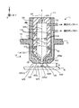
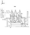
- FIG. 1 is a cross-sectional view showing the structure of the scanning electron microscope of the first embodiment.
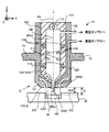
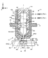
- FIG. 2 is a cross-sectional view showing the structure of a beam irradiation device included in the scanning electron microscope of the first embodiment.
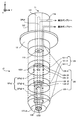
- FIG. 3 is a perspective view showing the structure of the beam irradiation device included in the scanning electron microscope of the first embodiment.
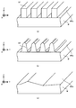
- FIGS. 4 (a) to 4 (c) is a perspective sectional view showing an example of the shape of the surface of the sample.
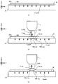
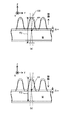
- FIGS. 5 (a) to 5 (c) is a cross-sectional view showing a process of deformation of the sample due to the formation of the vacuum region.
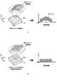
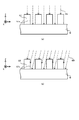
- FIG. 6A is an explanatory diagram showing image information and structural information showing the image and structure of the sample deformed due to the formation of the vacuum region, respectively
- FIG. 6B is an explanatory diagram of the undeformed sample. It is explanatory drawing which shows the image information and the structure information which shows the image and structure respectively.
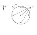
- FIG. 7 is a plan view showing an alignment mark formed on the sample W.
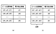
- FIG. 8A is an explanatory diagram showing the beam position information and the electron detection information before the change
- FIG. 8B is an explanatory diagram showing the beam position information and the electron detection information after the change. is there.
- FIG. 9A is an explanatory diagram showing the beam position information and the electron detection information before the change
- FIG. 9B is an explanatory diagram showing the beam position information and the electron detection information after the change. is there.
- FIG. 10 is a flowchart showing the flow of the sample information generation operation in the second modification.
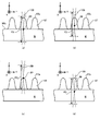
- FIGS. 11 (a) to 11 (d) is a cross-sectional view showing an initial position of the focus position.
- FIGS. 12 (a) to 12 (b) is a cross-sectional view showing an electron beam irradiated to a sample.
- FIG. 13 is a plan view showing image information (so-called SEM image) generated from the detection result of electrons by the electron detector in association with the cross section of the surface of the sample.
- SEM image image information
- FIG. 14 (a) to 14 (b) is a cross-sectional view showing an electron beam irradiated to a sample.
- FIG. 15 shows the structural information generated in the second modification in association with a plurality of image information and a cross section of the surface of the sample.
- FIGS. 16 (a) to 16 (b) is a cross-sectional view showing an electron beam irradiated to a sample.
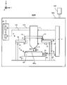
- FIG. 17 is a cross-sectional view showing the structure of the scanning electron microscope of the second embodiment.
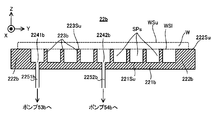
- FIG. 18 is a cross-sectional view showing the structure of the stage of the second embodiment.
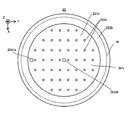
- FIG. 19 is a plan view showing the structure of the stage of the second embodiment.
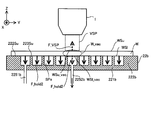
- FIG. 20 is a cross-sectional view showing a sample whose deformation is suppressed by the stage of the second embodiment.
- FIG. 21 is a cross-sectional view showing the structure of the stage of the third embodiment.
- FIG. 22 is a cross-sectional view showing the structure of the scanning electron microscope of the fourth embodiment.
- FIG. 23 is a cross-sectional view showing the structure of the scanning electron microscope of the fifth embodiment.
- FIG. 24 is a cross-sectional view showing the structure of the scanning electron microscope of the sixth embodiment.
- FIG. 25 is a cross-sectional view showing how the stage holds the sample in the first modification.
- FIG. 26 is a cross-sectional view showing how the stage holds the sample in the second modification.
- FIG. 27 is a cross-sectional view showing how the stage holds the sample in the third modification.
- Sample W is, for example, a semiconductor substrate.
- the sample W may be an object different from the semiconductor substrate.
- the sample W may be, for example, a disk-shaped substrate having a diameter of about 300 millimeters and a thickness of about 750 micrometers to 800 micrometers.
- the sample W may be a substrate (or an object) having an arbitrary size and an arbitrary shape.
- the sample W may be a square substrate for a display such as a liquid crystal display element or a square substrate for a photomask.
- each of the X-axis direction and the Y-axis direction is a horizontal direction (that is, a predetermined direction in the horizontal plane), and the Z-axis direction is a vertical direction (that is, a direction orthogonal to the horizontal plane). Yes, in effect, in the vertical direction).
- the + Z side corresponds to the upper side (that is, the upper side) and the ⁇ Z side corresponds to the lower side (that is, the lower side).
- the ⁇ Z direction may be referred to as a gravity direction.
- the Z-axis direction is also a direction parallel to the optical axis AX of the beam optical system 11 described later included in the scanning electron microscope SEM.
- the rotation directions (in other words, the inclination direction) around the X-axis, the Y-axis, and the Z-axis are referred to as the ⁇ X direction, the ⁇ Y direction, and the ⁇ Z direction, respectively.
- the wording "information about XX" includes not only information indicating XX directly but also information indicating an arbitrary parameter having some relation with XX.
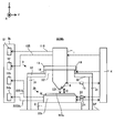
- FIG. 1 is a cross-sectional view showing the structure of the scanning electron microscope SEMa of the first embodiment.
- FIG. 2 is a cross-sectional view showing the structure of the beam irradiation device 1 included in the scanning electron microscope SEMa of the first embodiment.
- FIG. 3 is a perspective view showing the structure of the beam irradiation device 1 included in the scanning electron microscope SEMa of the first embodiment.
- FIG. 1 does not show a cross section of some components of the scanning electron microscope SEMa.
- the scanning electron microscope SEMa includes a beam irradiation device 1, a stage device 2, a support frame 3, a control device 4, a pump system 5, and a measuring device 6.
- the pump system 5 includes a vacuum pump 51 and a vacuum pump 52.
- the scanning electron microscope SEMa may include at least a chamber for accommodating the beam irradiation device 1, the stage device 2, and the support frame 3. Further, an air conditioner connected to this chamber and controlling the temperature and humidity of the space inside the chamber, particularly the space around the sample W may be provided.
- the beam irradiating device 1 can emit an electron beam EB downward from the beam irradiating device 1.
- the beam irradiating device 1 can irradiate the sample W held by the stage device 2 arranged below the beam irradiating device 1 with the electron beam EB.
- the beam irradiating device 1 includes a beam optical system 11 and a differential exhaust system 12 as shown in FIGS. 2 and 3.
- the beam optical system 11 includes a housing 111.
- the housing 111 is a cylindrical member in which a beam passing space SPb1 extending along the optical axis AX of the beam optical system 11 (that is, extending along the Z axis) is secured inside.
- the beam passing space SPb1 is used as a space through which the electron beam EB passes. To prevent the electron beam EB passing through the beam passing space SPb1 from passing through the housing 111 (that is, leaking to the outside of the housing 111) and / or the magnetic field outside the beam irradiation device 1 (so-called disturbance).
- the housing 111 may be made of a high magnetic permeability material in order to prevent the magnetic field) from affecting the electron beam EB passing through the beam passing space SPb1.
- high magnetic permeability materials include at least one of permalloy and silicon steel. The relative magnetic permeability of these high magnetic permeability materials is 1000 or more.
- the beam passing space SPb1 becomes a vacuum space during the period when the electron beam EB is irradiated.
- the beam passing space SPb1 has a pipe (that is, a pipe) formed in the housing 111 (furthermore, the side wall member 122 described later) so as to communicate with (that is, connect to) the beam passing space SPb1.
- the vacuum pump 51 is connected via a road) 118.
- the vacuum pump 51 exhausts the beam passing space SPb1 so that the beam passing space SPb1 becomes a vacuum space and reduces the pressure below the atmospheric pressure. Therefore, the vacuum space in the first embodiment may mean a space whose pressure is lower than the atmospheric pressure.
- the vacuum space is a space in which gas molecules exist only to the extent that the electron beam EB does not interfere with the appropriate irradiation of the sample W (in other words, the degree of vacuum does not interfere with the appropriate irradiation of the electron beam EB with the sample W).
- Space may be meant.
- the beam passing space SPb1 is a space outside the housing 111 (more specifically, a differential exhaust system 12 described later) via a beam ejection port (that is, an opening) 119 formed on the lower surface of the housing 111. It communicates with the beam passage space SPb2).
- the beam passing space SPb1 may be a vacuum space during the period when the electron beam EB is not irradiated.
- the beam optical system 11 further includes an electron gun 113, an electromagnetic lens 114, an objective lens 115, a deflector 116, and an electron detector 117.
- the electron gun 113 emits an electron beam EB toward the ⁇ Z side.
- a photoelectric conversion surface that emits electrons when irradiated with light may be used.
- the electromagnetic lens 114 controls the electron beam EB emitted by the electron gun 113.
- the electromagnetic lens 114 has an image rotation amount (that is, a position in the ⁇ Z direction) formed by the electron beam EB on a predetermined optical surface (for example, a virtual surface intersecting the optical path of the electron beam EB), and a magnification of the image.
- any one of the focal positions corresponding to the imaging position may be controlled.
- an electrostatic lens that controls the electron beam EB using an electric field may be used.
- the objective lens 115 is a surface on which the electron beam EB is irradiated with the electron beam EB at a predetermined reduction magnification (specifically, the surface on which the electron beam EB is irradiated, and faces the + Z side in the examples shown in FIGS. 1 and 2.
- a plane and a plane along the XY plane is imaged on WSu.
- the deflector 116 deflects the electron beam EB so that the irradiation position of the electron beam EB on the surface WSu of the sample W (particularly, the direction along the surface WSu (for example, the direction along at least one of the X-axis and the Y-axis)). ) Is controlled.
- the electron detector 117 is, for example, a semiconductor type electron detection device (that is, a semiconductor detection device) using a pn junction or pin junction semiconductor.
- the electron detector 117 for example, at least one of a detector using a scintillator (fluorescent substance) and a photomultiplier tube in combination and a micro-channel plate (MCP) may be used.
- the electron detector 117 detects the electrons generated by the irradiation of the sample W with the electron beam EB (that is, the electrons emitted from the sample W).
- the electrons generated by irradiating the sample W with the electron beam EB include, for example, at least one of the reflected electrons from the sample W and the scattered electrons from the sample W.
- the scattered electrons may include secondary electrons.
- the electronic detector 117 may be provided in the differential exhaust system 12 described later.
- the control device 4 acquires (in other words, obtains, calculates, or generates) information about the sample W based on the detection result of the electron detector 117.
- the differential exhaust system 12 includes a vacuum forming member 121 and a side wall member 122.
- the side wall member 122 is a tubular member extending upward from the vacuum forming member 121.
- the side wall member 122 houses the housing 111 (that is, the beam optical system 11) inside.
- the side wall member 122 is integrated with the beam optical system 11 with the beam optical system 11 housed therein, but may be separable from the beam optical system 11.
- the vacuum forming member 121 is arranged below the beam optical system 11 (that is, on the ⁇ Z side).
- the vacuum forming member 121 is connected (that is, connected) to the beam optical system 11 below the beam optical system 11.
- the vacuum forming member 121 is connected to the beam optical system 11 and integrated with the beam optical system 11, but may be separable from the beam optical system 11.
- a beam passing space SPb2 is formed inside the vacuum forming member 121.
- the vacuum forming member 121 is a vacuum forming member 121-1 in which the beam passing space SPb2-1 which is a part of the beam passing space SPb2 is formed, and the beam passing space which is a part of the beam passing space SPb2.
- the vacuum forming member 121-2 on which SPb2-2 is formed and the vacuum forming member 121-3 on which the beam passing space SPb2-3, which is a part of the beam passing space SPb2, are formed are separated from the beam passing space SPb2-1.
- the beam passage space SPb2 passes through a beam ejection port (that is, an opening) 1231 formed on the upper surface of the vacuum forming member 121 (in the example shown in FIG. 3, the surface on the + Z side of the vacuum forming member 121-3). It communicates with the beam passing space SPb1 of the optical system 11.
- the beam passing space SPb2 is exhausted (that is, depressurized) by the vacuum pump 51 together with the beam passing space SPb1. Therefore, the beam passing space SPb2 becomes a vacuum space during the period in which the electron beam EB is irradiated.
- the beam passing space SPb2 is used as a space through which the electron beam EB from the beam passing space SPb1 passes.
- the beam passing space SPb2 may be a vacuum space during the period when the electron beam EB is not irradiated.
- the vacuum forming member 121 further includes an injection surface 121LS capable of facing the surface WSu of the sample W.
- the vacuum forming member 121-1 includes an injection surface 121LS.
- the distance D between the injection surface 121LS and the surface WSu is a desired distance D_target (for example, 10 ⁇ m or less and 1 ⁇ m). The above) is aligned with the sample W by the interval adjusting system 14 described later.
- the distance D may be referred to as the distance between the injection surface 121LS and the surface WSu in the Z-axis direction.
- the interval adjusting system 14 may be referred to as an interval control device.
- a beam ejection port (that is, an opening) 1232 is formed on the ejection surface 121LS.
- the vacuum forming member 121 may not have an injection surface 121LS capable of facing the surface WSu of the sample W.
- the beam passing space SPb2 communicates with the beam passing space SPb3 outside the vacuum forming member 121 via the beam ejection port 1232. That is, the beam passing space SPb1 communicates with the beam passing space SPb3 via the beam passing space SPb2.
- the beam passage space SPb2 may not be secured. That is, the beam passing space SPb1 may be directly communicated with the beam passing space SPb3 without passing through the beam passing space SPb2.
- the beam passage space SPb3 is a space on the sample W (for example, a local space).
- the beam passage space SPb3 is a space through which the electron beam EB passes between the beam irradiation device 1 and the sample W (specifically, between the injection surface 121LS and the surface WSu).
- the beam passing space SPb3 is a space in the surface WSu of the sample W that at least faces (or covers or touches) the irradiation region irradiated with the electron beam EB.
- the beam passing space SPb3 is exhausted (that is, depressurized) by the vacuum pump 51 together with the beam passing spaces SPb1 and SPb2.
- each of the beam passing spaces SPb1 and SPb2 can also function as an exhaust passage (that is, a pipeline) connecting the beam passing space SPb3 and the vacuum pump 51 in order to exhaust the beam passing space SPb3. Therefore, the beam passing space SPb3 becomes a vacuum space during the period in which the electron beam EB is irradiated. Therefore, the electron beam EB emitted from the electron gun 113 irradiates the sample W through at least a part of the beam passing spaces SPb1 to SPb3, which are vacuum spaces.
- the beam passing space SPb3 may be a vacuum space during the period when the electron beam EB is not irradiated.
- the beam passing space SPb3 is located at a position farther from the vacuum pump 51 than the beam passing spaces SPb1 and SPb2.
- the beam passing space SPb2 is located at a position farther from the vacuum pump 51 than the beam passing space SPb1. Therefore, the degree of vacuum of the beam passing space SPb3 may be lower than the degree of vacuum of the beam passing spaces SPb1 and SPb2, and the degree of vacuum of the beam passing space SPb2 is higher than the degree of vacuum of the beam passing space SPb1. It can be low.
- the state of "the degree of vacuum in space B is lower than the degree of vacuum in space A" in the present embodiment means "the pressure in space B is higher than the pressure in space A".
- the vacuum pump 51 can set the vacuum degree of the beam passing space SPb3, which may have the lowest vacuum degree, to a vacuum degree that does not interfere with the appropriate irradiation of the electron beam EB to the sample W. Has exhaust capacity.
- the vacuum pump 51 maintains the pressure (ie, air pressure) of the beam passage space SPb3 below 1 ⁇ 10 -3 pascals (eg, approximately on the order of 1 ⁇ 10 -3 pascals to 1 ⁇ 10 -4 pascals). It may have an exhaust capacity that can be maintained).
- Such a vacuum pump 51 is used, for example, as a turbo molecular pump used as a main pump (or another type of high vacuum pump including at least one of a diffusion pump, a cryo pump and a sputter ion pump) and an auxiliary pump.
- a vacuum pump combined with a dry pump (or another type of low vacuum pump) may be used.
- the exhaust speed of the vacuum pump 51 may be an exhaust speed [m 3 / s] that can maintain the pressure (that is, atmospheric pressure) of the beam passing space SPb3 at 1 ⁇ 10 -3 pascal or less. ..
- the beam passing space SPb3 is not a closed space surrounded by some members (specifically, the housing 111 and the vacuum forming member 121) like the beam passing spaces SPb1 and SPb2. That is, the beam passing space SPb3 is an open space that is not surrounded by any member. Therefore, even if the beam passing space SPb3 is depressurized by the vacuum pump 51, gas flows into the beam passing space SPb3 from the periphery of the beam passing space SPb3. As a result, the degree of vacuum in the beam passing space SPb3 may decrease. Therefore, the differential exhaust system 12 maintains the degree of vacuum in the beam passing space SPb3 by performing differential exhaust between the beam irradiation device 1 and the sample W.
- the differential exhaust system 12 performs differential exhaust between the beam irradiation device 1 and the sample W, so that the vacuum between the beam irradiation device 1 and the sample W is relatively high as compared with the surroundings.
- a vacuum region VSP in which the degree is maintained (for example, a local vacuum region VSP) is formed.
- the beam irradiator 1 forms the vacuum region VSP so that the vacuum region VSP includes the beam passing space SPb3.
- the differential exhaust system 12 performs differential exhaust so that the beam passage space SPb3 is included in the vacuum region VSP.
- the air pressure between the sample W and the beam irradiator 1 is between one space (for example, the beam passing space SPb3) and another space different from the one space.
- the beam passage space SPb3 covers at least a part of the surface WSu of the sample W (for example, the irradiation region where the electron beam EB is irradiated), the vacuum region VSP is also at least one of the surface WSu of the sample W. The portion (for example, the irradiation area where the electron beam EB is irradiated) is locally covered.
- an exhaust groove that is, an opening that does not penetrate the vacuum forming member 121) 124 that surrounds the beam injection port 1232 is formed on the injection surface 121LS of the vacuum forming member 121.
- the vacuum pump 52 is connected to the exhaust groove 124 via a pipe (that is, a pipeline) 125 formed in the vacuum forming member 121 and the side wall member 122 so as to communicate with the exhaust groove 124.
- the first end (ie, one end) of the pipe 125 is connected to the vacuum pump 52 and is the second end (ie, the other end) of the pipe 125, substantially forming the exhaust groove 124.
- the portion is in contact with the space between the injection surface 12LS and the surface WSu of the sample W. Note that FIG.
- FIG. 3 shows an example in which the differential exhaust system 12 has a structure in which the pipes 125 are integrated from the exhaust groove 124 to the vacuum pump 52.
- FIG. 3 shows an annular flow path 125 extending upward from the annular exhaust groove 124 to the vacuum forming member 121-1 in which the exhaust groove 124 is formed so as to penetrate the vacuum forming member 121-1. -1 is formed, and N1 pipes 125-21 and N1 pipes 125-21 that communicate with the flow path 125-1 are integrated into the vacuum forming member 121-2 (4 in the example shown in FIG. 3).
- An annular integrated flow path 125-22 is formed, and N2 (however, N2 ⁇ N1) lines communicating with the centralized flow path 125-22 are formed in the vacuum forming member 121-3 (two lines in the example shown in FIG. 3).
- An annular integrated flow path 125-32 for consolidating the pipes 125-31 and N2 pipes 125-31 is formed, and the pipe 125-4 (that is, the pipe formed on the side wall member 122) is formed in the integrated flow path 125-32.
- An example is shown in which 125-4) communicates and the pipe 125-4 is connected to the vacuum pump 52. In the example shown in FIG.
- the number N2 of the pipes 125-31 is half the number N1 of the pipes 125-21, and one pipe 125-31 is substantially equal to the two pipes 125-21 communicating with the pipe 125-31. It is located equidistant. Further, the number N2 of the pipes 125-31 is half the number of the pipes 125-4 (one in the example shown in FIG. 3), and the pipes 125-4 are substantially equal to the two pipes 125-31 communicating with the pipes 125-4. It is located equidistant. Therefore, the length and pressure loss of the exhaust path through the respective pipes 125-21 are substantially equal, and the amount of air exhausted from the exhaust groove 124 is not biased regardless of the orientation.
- the structure of the pipe 125 is not limited to this example.
- the vacuum pump 52 exhausts the space around the beam passing space SPb3 through the exhaust groove 124.
- the exhaust groove 124 does not have to be an annular shape connected to one, and may be a plurality of exhaust grooves having a plurality of a part of the ring.
- the vacuum pump 52 is mainly used to exhaust the space around the beam passing space SPb3 in order to make the degree of vacuum of the beam passing space SPb3 relatively high. Therefore, the vacuum pump 52 may have an exhaust capacity capable of maintaining a vacuum degree lower than the vacuum degree maintained by the vacuum pump 51. That is, the exhaust capacity of the vacuum pump 52 may be lower than the exhaust capacity of the vacuum pump 51.
- the vacuum pump 52 may be a vacuum pump that includes a dry pump (or another type of low vacuum pump) but not a turbo molecular pump (or another type of high vacuum pump). Good.
- the degree of vacuum in the space in the exhaust groove 124 and the pipe 125 decompressed by the vacuum pump 52 may be lower than the degree of vacuum in the beam passage spaces SPb1 to SPb3 decompressed by the vacuum pump 51.
- the exhaust speed of the vacuum pump 52 may be an exhaust speed [m 3 / s] that can maintain a vacuum degree lower than the vacuum degree maintained by the vacuum pump 51.
- the vacuum region VSP including the beam passage space SPb3 is formed in this way, at least the portion of the surface WSu of the sample W that does not face the beam passage space SPb3 (particularly, the portion away from the beam passage space SPb3).
- a part may be covered with a non-vacuum region having a lower degree of vacuum than the vacuum region VSP.
- at least a part of the surface WSu of the sample W that does not face the beam passage space SPb3 may be in an atmospheric pressure environment. That is, at least a part of the surface WSu of the sample W that does not face the beam passing space SPb3 may be covered with the atmospheric pressure region.
- the differential exhaust system 12 forms a vacuum region VSP in the space SP1 (see FIG.
- This space SP1 includes, for example, a space in contact with at least one of the beam injection port 1232 and the exhaust groove 124.
- the space SP1 includes a space facing (that is, in contact with) a portion of the surface WSu of the sample W located directly below at least one of the beam injection port 1232 and the exhaust groove 124.
- the vacuum region VSP is provided in the space SP2 around the space SP1 (that is, the space SP2 connected to the space SP1 (for example, fluidly connected) around the space SP1 and see FIG. 2).
- the space SP2 is a space having a higher pressure than the space SP1.
- This space SP2 includes, for example, a space away from the beam ejection port 1232 and the exhaust groove 124.
- the space SP2 includes, for example, a space facing a portion of the surface WSu of the sample W that is different from the portion facing the space SP1.
- the space SP2 includes a space that cannot be connected to the beam injection port 1232 and the exhaust groove 124 (furthermore, the beam passage space SPb2 and the pipe 125) without passing through the space SP1.
- the space SP2 includes a space that can be connected to the beam injection port 1232 and the exhaust groove 124 (further, the beam passage space SPb2 and the pipe 125) via the space SP1.
- the pressure in the space SP2 is higher than the pressure in the space SP1, there is a possibility that the gas flows from the space SP2 into the space SP1, but the gas flowing from the space SP2 into the space SP1 is exhaust groove 124 ( Further, it is discharged from the space SP1 via the beam ejection port 1232). That is, the gas flowing from the space SP2 into the space SP1 is discharged from the space SP1 via the pipe 125 (furthermore, the beam passing space SPb2). Therefore, the degree of vacuum of the vacuum region VSP formed in the space SP1 is maintained.
- the state in which the vacuum region VSP is locally formed is the state in which the vacuum region VSP is locally formed on the surface WSu of the sample W (that is, the vacuum region VSP is formed in the direction along the surface WSu of the sample W). May mean a state in which is locally formed).
- the stage device 2 is arranged below the beam irradiation device 1 (that is, on the ⁇ Z side).
- the stage device 2 includes a surface plate 21 and a stage 22.
- the surface plate 21 is arranged on a support surface SF such as a floor.
- the stage 22 is arranged on the surface plate 21.
- a vibration isolator (not shown) is installed between the stage 22 and the surface plate 21 to prevent the vibration of the surface plate 21 from being transmitted to the stage 22.
- the stage 22 can hold the sample W.
- the stage 22 may hold the sample W by vacuum-adsorbing or electrostatically adsorbing the sample W.
- the stage 22 can release the retained sample W.
- the stage 22 can move along at least one of the X-axis direction, the Y-axis direction, the Z-axis direction, the ⁇ X direction, the ⁇ Y direction, and the ⁇ Z direction while holding the sample W under the control of the control device 4. ..
- the stage device 2 includes a stage drive system 23.
- the stage drive system 23 moves the stage 22 by using, for example, an arbitrary motor (for example, a linear motor or the like).
- the stage device 2 includes a position measuring device 24 for measuring the position of the stage 22.
- the position measuring device 24 includes, for example, at least one of an encoder and a laser interferometer.
- the control device 4 can specify the position of the sample W from the position of the stage 22.
- the stage 22 may have a reference plate provided with a reference mark for associating the position of the electron beam EB by the beam irradiation device 1 with the position of the stage 22 (position in the XYZ direction).
- the relative position of the sample W and the beam irradiator 1 in the direction along the XY plane changes. Therefore, when the stage 22 moves along the XY plane, the relative positions of the sample W and the irradiation region of the electron beam EB on the surface WSu of the sample W in the direction along the XY plane change. That is, when the stage 22 moves along the XY plane, the irradiation region of the electron beam EB moves with respect to the surface WSu of the sample W in the direction along the XY plane (that is, the direction along the surface WSu of the sample W). To do.
- the relative positions of the sample W and the beam passing space SPb3 and the vacuum region VSP in the direction along the XY plane change. That is, when the stage 22 moves along the XY plane, the beam passage space SPb3 and the vacuum region VSP with respect to the surface WSu of the sample W in the direction along the XY plane (that is, the direction along the surface WSu of the sample W).
- the control device 4 controls the stage drive system 23 so that the electron beam EB is irradiated to a desired position on the surface WSu of the sample W and the beam passage space SPb3 is set (that is, the vacuum region VSP is formed).
- the stage 22 may be moved along the XY plane.
- the relative position of the sample W and the beam irradiator 1 in the direction along the Z axis changes. Therefore, when the stage 22 moves along the Z axis, the relative position between the sample W and the focus position FP of the electron beam EB in the direction along the Z axis changes.
- the control device 4 controls the stage drive system 23 so that the focus position FP of the electron beam EB is set on the surface WSu of the sample W (or in the vicinity of the surface WSu) so that the stage 22 is moved along the Z axis. You may move it.
- the focus position FP of the electron beam EB may be a focus position corresponding to the image formation position of the beam optical system 11 or a position in the Z-axis direction that minimizes the blurring of the electron beam EB.
- the stage drive system 23 may move the stage 22 under the control of the control device 4 so that the interval D becomes a desired interval D_taget in cooperation with the interval adjusting system 14 described later.
- the control device 4 is based on the measurement result of the position measurement device 24 (furthermore, the measurement result of the position measurement device 15 that measures the position of the beam irradiation device 1 (particularly, the position of the vacuum forming member 121) described later). Therefore, the actual interval D is specified, and at least one of the stage drive system 23 and the interval adjusting system 14 is controlled so that the specified interval D becomes the desired interval D_taget.
- the position measuring devices 15 and 24 can also function as detection devices for detecting the interval D.
- the control device 4 replaces or adds to the actual interval D with the beam irradiation device 1 and the reference surface (for example, the surface of the reference plate).
- the distance D between the beam irradiation device 1 and the sample W is set to the desired distance D_taget. At least one of the stage drive system 23 and the interval adjustment system 14 may be controlled.
- the support frame 3 supports the beam irradiation device 1.
- the support frame 3 includes support legs 31 and support members 32.
- the support legs 31 are arranged on the support surface SF.
- a vibration isolator (not shown) may be installed between the support leg 31 and the support surface SF to prevent or reduce the transmission of the vibration of the support surface SF to the support leg 31.
- the support leg 31 is, for example, a member extending upward from the support surface SF.
- the support legs 31 support the support member 32.
- the support member 32 is an annular plate member having an opening 321 formed in the center in a plan view. The upper surface of the support member 32 extends outward from the outer surface of the beam irradiation device 1 (in the example shown in FIGS.
- the support frame 3 can support the beam irradiation device 1 so as to be lifted by the upper surface of the support member 32.
- the support frame 3 may function as a stopper for preventing the beam irradiation device 1 from moving toward the sample W so as to prevent the beam irradiation device 1 from colliding with the sample W.
- the support frame 3 may support the beam irradiation device 1 by a support method different from the support method shown in FIG.
- the support frame 3 may be supported by a suspension support mechanism.
- the anti-vibration pad is fixed to the top plate (ceiling wall) of the chamber accommodating the support frame 3, one end is connected to the lower end of the anti-vibration pad, and the other end of the wire made of steel is connected to the support frame 3.
- the anti-vibration pad may include, for example, an air damper and / or a coil spring.
- An anti-vibration device (not shown) may be installed between the support legs 31 and the support member 32 to prevent or reduce the transmission of the vibration of the support surface SF to the support member 32.
- the interval adjusting system 14 moves the interval D (or the vacuum forming member 121) between the injection surface 121LS of the vacuum forming member 121 and the surface WSu of the sample W.
- the distance in the Z-axis direction from the injection surface 121LS to the surface WSu of the sample W) is adjusted.
- the interval adjusting system 14 may move the beam irradiation device 1 along the Z-axis direction so that the interval D becomes a desired interval D_taget.
- an interval adjusting system 14 for example, a drive system that moves the beam irradiation device 1 by using the driving force of the motor, and a drive system that moves the beam irradiation device 1 by using the force generated by the piezoelectric effect of the piezo element.
- a drive system that moves the beam irradiation device 1 using a Coulomb force (for example, an electrostatic force generated between at least two electrodes) and a Lorentz force (for example, an electromagnetic force generated between a coil and a magnetic pole) are used.
- At least one of the drive systems for moving the beam irradiation device 1 may be used.
- the interval adjusting system 14 may move the beam irradiation device 1 along at least one of the X-axis direction, the Y-axis direction, the ⁇ X direction, the ⁇ Y direction, and the ⁇ Z direction. In this case, the interval adjusting system 14 may be referred to as a position changing device.
- the scanning electron microscope SEMa includes a position measuring device 15.
- the position measuring device 15 includes, for example, at least one of an encoder and a laser interferometer.
- the position measuring device 15 may measure the position of the beam irradiation device 1 in the XY direction, the posture in the ⁇ X direction, and the posture in the ⁇ Y direction.
- a measuring device for measuring the position of the beam irradiation device 1 in the XY direction, the posture in the ⁇ X direction, and the posture in the ⁇ Y direction may be provided separately from the position measuring device 15.
- the control device 4 controls the operation of the scanning electron microscope SEMa.
- the control device 4 controls the beam irradiation device 1 so as to irradiate the sample W with the electron beam EB.
- the control device 4 controls the pump system 5 (particularly, the vacuum pumps 51 and 52) so that the beam passing spaces SPb1 to SPb3 are made into a vacuum space. At this time, the degree of vacuum of the beam passing spaces SPb1, SPb2 and SPb3 does not have to be the same.
- the control device 4 controls at least one of the stage drive system 23 and the deflector 116 so that the electron beam EB is irradiated to a desired position in the XY plane of the surface WSu of the sample W.
- control device 4 controls the interval adjusting system 14 so that the interval D between the injection surface 121LS of the vacuum forming member 121 and the surface WSu of the sample W is a desired interval D_taget.
- control device 4 includes, for example, an arithmetic unit such as a CPU (Central Processing Unit), a DSP (Digital Signal Processor), an MCU (Micro Control Unit), and a memory. It may include at least one of the storage devices.
- the control device 4 irradiates the sample W with the electron beam EB so as to scan the surface WSu of the sample W with the electron beam EB, for example.
- the scanning electron microscope SEMa controls the stage drive system 23 to move the stage 22 along the XY plane so that the vacuum region VSP is formed on the first surface portion of the surface WSu of the sample W. Let me. After the stage 22 moves so that the vacuum region VSP is formed on the first surface portion of the surface WSu of the sample W, the beam irradiation device 1 irradiates the first surface portion of the surface WSu of the sample W with the electron beam EB. ..
- the beam irradiation device 1 scans the first surface portion with the electron beam EB by deflecting the electron beam EB using the deflector 116.
- the stage drive system 23 does not have to move the stage 22 along the XY plane.
- the scanning electron microscope SEMa controls the stage drive system 23 so that the vacuum region VSP is formed on the second surface portion of the surface WSu of the sample W. Then, the stage 22 is moved along the XY plane.
- the beam irradiation device 1 irradiates the second surface portion of the surface WSu of the sample W with the electron beam EB. ..
- the beam irradiator 1 scans the second surface portion with the electron beam EB by deflecting the electron beam EB using the deflector 116.
- the stage drive system 23 does not have to move the stage 22 along the XY plane also during the period in which the beam irradiation device 1 irradiates the second surface portion of the surface WSu of the sample W with the electron beam EB. After that, the same process is repeated until the irradiation (that is, scanning) of the electron beam EB on the target region of the surface WSu of the sample W to be irradiated with the electron beam EB is completed.
- the control device 4 generates (that is, acquires) information about the sample W based on the detection result of the electron detector 117.
- the electron detector 117 detects, for example, the amount of electrons (for example, at least one of reflected electrons and scattered electrons) generated when the sample W is irradiated with the electron beam EB. Therefore, the detection result of the electron detector 117 may include information on the detection amount of electrons generated when the sample W is irradiated with the electron beam EB.
- the detection result of the electron detector 117 may be, in addition to or in place of the information regarding the amount of detected electrons, information about the electrons generated when the sample W is irradiated with the electron beam EB (for example, the velocity and the angle of incidence of the electrons). Information on at least one of the above) may be included.
- the control device 4 may generate information regarding the image of the sample W (hereinafter referred to as “image information”) based on the detection result of the electronic detector 117.
- the image information may include information about the image of the surface WSu of the sample W.
- the electron detector 117 detects the electrons generated when the electron beam EB is irradiated while the beam optical system 11 is scanning the surface WSu of the sample W with the electron beam EB.
- the electron detector 117 is, for example, the electrons generated when the electron beam EB is irradiated to the first position of the surface WSu of the sample W, the sample W.
- the control device 4 can generate information on the distribution of the detected amount of electrons based on the detection result of the electron detector 117. That is, the control device 4 has an image having characteristics according to the amount of detected electrons based on the detection result of the electron detector 117 (that is, information on the detection result of electrons) and the information on the irradiation position of the electron beam EB. Image information regarding (a so-called SEM image, and in the first embodiment, an image of the surface WSu of the sample W) can be generated.
- the characteristic of the image may be at least one of contrast, brightness and SN (Signal to Noise) ratio. That is, the image indicated by the image information may be an image having a contrast distribution according to the detection amount of electrons, an image having a brightness distribution according to the detection amount of electrons, or detection of electrons.
- the image may have an SN ratio distribution according to the amount.
- the amount of electrons detected when each portion of the surface WSu of the sample W is irradiated with the electron beam EB depends on the structure of the surface WSu of the sample W (for example, a three-dimensional structure). Therefore, it can be said that the image shown by the image information has a contrast distribution (or a luminance distribution or an SN ratio distribution) according to the structure of the surface WSu of the sample W.
- Information on the irradiation position of the electron beam EB used for generating image information can be specified from, for example, the exciting current flowing through the deflector 116 that deflects the electron beam EB and controls the irradiation position of the electron beam EB. is there. That is, the control device 4 relates to the irradiation position of the electron beam EB from the exciting current flowing through the deflector 116 based on the correlation information that defines the correlation between the exciting current flowing through the deflector 116 and the irradiation position of the electron beam EB. Information can be identified.
- the control device 4 may periodically (or at a desired timing) modify the correlation information that defines the correlation between the exciting current flowing through the deflector 116 and the irradiation position of the electron beam EB. Specifically, the control device 4 controls the beam irradiation device 1 and the stage device 2 so as to irradiate the electron beam EB to the mark formed at a specific position on the stage 22 (or the reference plate described above). At the same time, the correlation information may be modified based on the exciting current at that time and the position of the stage 22.
- the control device 4 detects the irradiation position of the electron beam EB and the electron detector 117.
- the electron beam EB is irradiated to the irradiation position (x, y, z) and the irradiation position (x, y, z) of the electron beam EB in the XYZ orthogonal coordinate system based on the detected amount of electrons.
- the function S s (x, y, z) indicating the relationship with the amount S of electrons generated in (that is, the state of distribution of the detected amount of electrons described above) may be specified.
- control device 4 may generate image information based on the function s (x, y, z).
- Such image information includes information on the structure (for example, three-dimensional structure) of the surface WSu of the sample W. Therefore, the control device 4 may specify the structure (for example, three-dimensional structure) of the surface WSu of the sample W based on the image information. That is, the control device 4 may generate structural information regarding the structure of the surface WSu of the sample W (for example, a three-dimensional structure) based on the image information (that is, based on the detection result of the electron detector 117). ..
- the structural information may include information on the positions of each unit surface portion in the X-axis direction, the Y-axis direction, and the Z-axis direction when the surface WSu is divided into a plurality of unit surface portions.
- the structural information is the orientation of each unit surface portion (for example, the orientation of the normal of each unit surface portion, and is substantially equivalent to the amount of inclination of each unit surface portion with respect to at least one of the X-axis, Y-axis, and Z-axis. ) May be included.
- the structural information may include information regarding a three-dimensional model of the surface WSu (so-called three-dimensional profile information).
- the surface WSu of the sample W is ideally flat
- the control device 4 is an image relating to an image of the surface WSu including an image of a structure of a fine uneven pattern formed on the surface WSu. It is assumed that information (or structural information regarding the structure of the surface WSu including the structure of the uneven pattern) is generated.
- the surface WSu of the sample W does not have to be flat.
- the control device 4 when a fine concavo-convex structure ST is formed on the surface WSu of the sample W, the control device 4 is a concavo-convex structure. Generates structural information regarding the structure of the surface WSu of sample W, including the structure of ST.
- the structural information is substantially information about the height of the concave-convex structure ST (that is, the size in the Z-axis direction) and the width of the concave-convex structure ST (that is, at least one of the X-axis direction and the Y-axis direction).
- an example of the concave-convex structure ST is a circuit pattern (for example, at least one of a line-and-space pattern and an isolated pattern) constituting a semiconductor circuit. ..
- a resist pattern formed on a semiconductor substrate to form a semiconductor circuit.
- the control device 4 can be used on the surface WSu of the sample W.
- Structural information about the structure may be generated. In this case, it can be said that the structural information substantially includes information on the roughness of the surface WSu.
- a vacuum region VSP is formed on the surface WSu of the sample W.
- the control device 4 cannot generate appropriate image information and / or structural information.
- FIGS. 5 (a) to 5 (c) since both the image information and the structural information are information related to the sample W, the image information and the structural information are collectively referred to as “sample information” to proceed with the description.
- the stage 22 vacuum-adsorbs or electrostatically adsorbs the sample W as described above.
- the force that attracts the sample W to the stage 22 acts on the sample W.
- the stage 22 vacuum-adsorbs the sample W
- the force caused by the negative pressure generated on the back surface WSl of the sample W attracts the back surface WSl of the sample W to the stage 22 (that is, the sample W). It acts as a force to attract to the stage 22).
- the stage 22 electrostatically attracts the sample W
- the electrostatic force generated in the sample W acts as a force for attracting the sample W to the stage 22.
- the stage 22 uses the force F_hold1 acting on the sample W (particularly, the back surface WSl of the sample W) due to this vacuum adsorption or electrostatic adsorption as a force for holding the sample W, thereby causing the sample W. To hold.
- a vacuum region VSP is formed between the beam irradiation device 1 and the sample W as shown in FIG. 5B.
- the vacuum surface portion WSu_vac facing the vacuum region VSP (that is, facing the beam passing space SPb3) has a force (that is, the vacuum region VSP) caused by the formation of the vacuum region VSP.
- the force that attracts the surface WSu of the sample W) F_VSP acts.
- the force F_hold1 caused by vacuum adsorption or electrostatic adsorption still acts on the vacuum surface portion WSl_vac corresponding to the vacuum surface portion WSu_vac in the back surface WSl of the sample W.
- the force F_VSP acting on the vacuum surface portion WSu_vac indirectly acts on the specific portion W_vac of the sample W facing the vacuum region VSP (that is, facing the beam passage space SPb3).
- the force F_hold1 acting on the vacuum surface portion WSl_vac also acts indirectly on the specific portion W_vac (or the vacuum surface portion WSu_vac). That is, in the specific portion W_vac of the sample W, the force acting on the sample W from the vacuum region VSP (that is, the force that the vacuum region VSP sucks the sample W) F_VSP and the force acting on the sample W from the stage 22 (that is, that is).
- the force F_vac that is the sum of the force F_hold1 that the stage 22 holds the sample W acts on.
- the force F_VSP becomes larger than the force F_hold1
- the force F_vac acting on the specific portion W_vac becomes a force that attracts the specific portion W_vac to the vacuum region VSP. That is, the specific portion W_vac is separated from the stage 22 due to the formation of the vacuum region VSP on the specific portion W_vac on which the force F_hold1 that presses the specific portion W_vac against the stage 22 acts before the formation of the vacuum region VSP.
- the force F_vac acts.
- the specific portion W_vac has a force F_vac that pushes or pulls away (that is, displaces) the specific portion W_vac in the direction from the stage 22 toward the beam irradiation device 1 due to the formation of the vacuum region VSP. It works.
- the force F_vac that separates the specific portion W_vac from the stage 22 due to the formation of the vacuum region VSP acts on the specific portion W_vac, as shown in FIG. 5C, the specific portion W_vac of the sample W is removed from the stage 22. May be pulled apart.
- the vacuum region VSP is not formed in the portion of the sample W other than the specific portion W_vac. Therefore, the force F_hold1 that presses the other portion against the stage 22 still acts on the portion of the sample W other than the specific portion W_vac. That is, the portion of the sample W other than the specific portion W_vac is not easily separated from the stage 22. As a result, as shown in FIG. 5C, the sample W may be deformed.
- the sample W is typically deformed so that the position of at least a part of the sample W changes in the direction along the optical axis AX of the beam optical system 11 (that is, the Z-axis direction and the vertical direction).
- the sample W is at least a part of the position of the sample W in the direction along the plane intersecting the optical axis AX of the beam optical system 11 in addition to or instead of the direction along the optical axis AX of the beam optical system 11. It may be transformed so that For example, the sample W changes the position of at least a part of the sample W in the direction along the plane orthogonal to the optical axis AX of the beam optical system 11 (that is, the plane which is the XY plane and is parallel to the horizontal plane). It may be deformed.
- the control device 4 may generate image information regarding the image of the surface Wsu of the sample W deformed due to the formation of the vacuum region VSP.
- the control device 4 includes an image including an error component (for example, an offset component due to the deformation) related to the deformation of the sample W due to the formation of the vacuum region VSP. May generate information. That is, the control device 4 may not be able to generate image information that is originally desired to be generated or should be generated (that is, ideal image information that does not include an error component regarding deformation of the sample W due to the formation of the vacuum region VSP). There is sex. Specifically, as shown on the left side of FIG.
- the control device 4 is a surface WSu of the undeformed sample W (that is, the sample W in which the vacuum region VSP is not formed on the surface WSu). It may not be possible to generate image information about the image. Similarly, the control device 4 may generate structural information regarding the structure of the surface Wsu of the sample W deformed due to the formation of the vacuum region VSP. Specifically, as shown on the right side of FIG. 6A, the control device 4 may generate structural information including an error component regarding the deformation of the sample W due to the formation of the vacuum region VSP.
- control device 4 may not be able to generate structural information that is originally desired to be generated or should be generated (that is, ideal structural information that does not include an error component regarding deformation of the sample W due to the formation of the vacuum region VSP). There is sex. Specifically, as shown on the right side of FIG. 6B, the control device 4 is a surface WSu of the undeformed sample W (that is, the sample W in which the vacuum region VSP is not formed on the surface WSu). It may not be possible to generate structural information about the structure.
- the same technical problem occurs not only when the sample W is deformed due to the formation of the vacuum region VSP but also when the sample W is deformed due to a factor different from the formation of the vacuum region VSP. .. That is, depending on the shape of the sample W held by the scanning electron microscope SEMa, the scanning electron microscope SEMa may not be able to generate appropriate sample information. For example, if the actual shape of the sample W during the period of irradiation with the electron beam EB is different from the original shape of the sample W, the scanning electron microscope SEMa cannot generate appropriate sample information. there is a possibility.
- the scanning electron microscope SEMa has an ideal shape (for example, not deformed or the original shape) under the control of the control device 4 without depending on the shape of the sample W.
- an ideal shape for example, not deformed or the original shape
- the influence of the difference in the shape of the sample W is suppressed.
- the scanning electron microscope SEMa is not deformed (or is not deformed) even when the sample W is deformed due to the formation of the vacuum region VSP or the like under the control of the control device 4.
- Deformation suppression operation that suppresses the influence of deformation of sample W by generating image information about the image of sample W and / or structural information about the structure of sample W that is not deformed. I do.
- the deformation suppressing operation will be further described.
- the scanning electron microscope SEMa first generates shape information regarding the shape (particularly, three-dimensional shape) of the sample W.
- the shape information may be information on the overall shape of the sample W (for example, the overall shape of the surface WSu of the sample W), or a part of the shape of the sample W (for example, the surface WSu of the sample W). It may be information about some shapes).
- the scanning electron microscope SEMa irradiates the sample W with the electron beam EB.
- the electron detector 117 detects the electrons generated when the electron beam EB is irradiated.
- the scanning electron microscope SEMa After that, the scanning electron microscope SEMa generates image information and / or structural information based on the detection result of the electron detector 117. At this time, the scanning electron microscope SEMa relates to the image information regarding the image of the undeformed sample W and / or the structure of the undeformed sample W based on the shape information in addition to the detection result of the electron detector 117. Generate structural information.
- shape information an operation of generating shape information and an operation of generating image information and / or structural information (that is, sample information) will be described in order.
- the sample W is the sample W in the direction along the optical axis AX of the beam optical system 11 (that is, the Z-axis direction and the vertical direction). At least one of the samples W is deformed so as to change at least a part of the position, and at least one of the samples W is oriented along a plane intersecting the optical axis AX of the beam optical system 11 (for example, a plane which is an XY plane and is parallel to a horizontal plane). It may be deformed so that the position of the part changes.
- the shape information also includes X shape information regarding the shape of the surface WSu of the sample W in the X axis direction, Y shape information regarding the shape of the surface WSu of the sample W in the Y axis direction, and Z axis of the surface WSu of the sample W. It may include Z-shape information about the shape in the direction.
- the X-shape information may include X-position information regarding the position of each portion of the surface WSu in the X-axis direction.
- the Y-shape information may include Y-position information regarding the position of each portion of the surface WSu in the Y-axis direction.
- the Z shape information may include Z position information regarding the position of each portion of the surface WSu in the Z axis direction.
- the design position of each part of the surface WSu of the sample (that is, the position of each part of the surface WSu of the sample W that is not deformed or has an ideal shape) is known information for the scanning electron microscope SEMa. ..
- the shape information may include deformation information regarding the amount of deformation of the surface WSu of the sample W.
- the X shape information may include X deformation information regarding the amount of deformation of the surface WSu of the sample W in the X axis direction.
- the amount of deformation of the surface WSu of the sample W in the X-axis direction indicates the amount of deviation in the X-axis direction between the actual position of each portion of the surface WSu and the design position.
- the Y shape information may include Y deformation information regarding the amount of deformation of the surface WSu of the sample W in the Y axis direction.
- the amount of deformation of the surface WSu of the sample W in the Y-axis direction indicates the amount of deviation in the Y-axis direction between the actual position of each portion of the surface WSu and the design position.
- the Z shape information may include Z deformation information regarding the amount of deformation of the surface WSu of the sample W in the Z axis direction.
- the amount of deformation of the surface WSu of the sample W in the Z-axis direction indicates the amount of deviation in the Z-axis direction between the actual position of each portion of the surface WSu and the design position.
- the scanning electron microscope SEMa may use the alignment mark AM formed in advance on the sample W.
- at least one alignment mark AM is formed on the sample W (particularly, its surface WSu) as shown in FIG.
- FIG. 7 shows an example in which five alignment mark AMs are formed, the number of alignment mark AMs is not limited to five, and the arrangement position thereof is limited to the example shown in FIG. There is nothing.
- Each alignment mark AM has an X mark for generating X shape information (for example, a mark having periodicity in the X axis direction) and a Y mark for generating Y shape information (for example, a mark having periodicity in the Y axis direction). A mark) and may be included.
- the scanning electron microscope SEMa irradiates the alignment mark AM with the electron beam EB under the control of the control device 4, and detects the reflected electrons from the alignment mark AM with the electron detector 117.
- the position measurement system 24 also measures the position of the stage 22.
- the control device 4 is based on the detection result of the electron detector 117 (that is, the detection result of the reflected electrons from the alignment mark AM) and the measurement result of the position measurement system 24 (that is, the measurement result of the position of the stage 22).
- the position of the alignment mark AM in each of the X-axis direction and the Y-axis direction (that is, the position of the portion of the surface WSu of the sample W where the alignment mark AM is formed) is specified.
- control device 4 After that, the control device 4 performs statistical processing (for example, statistical processing based on EGA: Enhanced Global Alignment) on the information regarding the positions of the plurality of alignment mark AMs, thereby performing the X-axis of each part of the surface WSu of the sample W. Estimate the position in each of the direction and the Y-axis direction. As a result, the control device 4 can generate X shape information and Y shape information based on the estimated position.
- statistical processing for example, statistical processing based on EGA: Enhanced Global Alignment
- the scanning electron microscope SEMa may use a method different from the method for generating X shape information and Y shape information.
- the scanning electron microscope SEMa may use the measuring device 6 provided in the scanning electron microscope SEMa in order to generate Z shape information.
- the measuring device 6 is a device used for measuring the shape of the surface WSu of the sample W in the Z-axis direction.
- the measuring device 6 may optically measure the shape of the surface WSu of the sample W in the Z-axis direction.
- the measuring device 6 may use the so-called autofocus method for measuring the shape of the surface WSu of the sample W in the Z-axis direction.
- the measuring device 6 uses an irradiation optical system (for example, an optical system including a light source) for irradiating the sample W with measurement light (for example, at least one of visible light and infrared light) and the sample W. It may be provided with a detection optical system (for example, an optical system including an optical sensor) for detecting the measurement light.
- the detection result of the measurement light by the detection optical system is output to the control device 4.
- the control device 4 irradiates the sample W with the measurement light and the sample W is irradiated with the measurement light during the period from when the sample W is irradiated with the measurement light until the measurement light via the sample W is detected by the detection optical system.
- the sample W (particularly, the portion irradiated with the measurement light) from the measuring device 6 ) Can be specified. Assuming that the position of the measuring device 6 is fixed (that is, the position of the measuring device 6 is known information), the specified distance is substantially the sample W (particularly, the measurement light is irradiated). Part) is equivalent to the position in the Z-axis direction.
- the control device 4 can display the Z of each portion of the surface WSu of the sample W.
- the position in the axial direction can be estimated.
- the control device 4 can generate Z shape information based on the estimated position.
- the scanning electron microscope SEMa Even if the scanning electron microscope SEMa generates shape information in a state where the scanning electron microscope SEMa actually forms the vacuum region VSP in order to irradiate the sample W with the electron beam EB to generate sample information. Good. That is, in the scanning electron microscope SEMa, the alignment mark AM is irradiated with the electron beam EB in a state where the scanning electron microscope SEMa actually forms the vacuum region VSP in order to generate sample information, and the X shape information and the X shape information and In addition to generating Y-shape information, Z-shape information may be generated using the measuring device 6.
- the scanning electron microscope SEMa may generate shape information before the scanning electron microscope SEMa actually forms the vacuum region VSP in order to generate sample information. That is, in the scanning electron microscope SEMa, the alignment mark AM is irradiated with the electron beam EB before the scanning electron microscope SEMa actually forms the vacuum region VSP in order to generate sample information, and the X shape information and the Y shape are obtained. In addition to generating information, Z-shape information may be generated using the measuring device 6. However, in this case, in the scanning electron microscope SEMa, another vacuum region VSP'having the same characteristics as the vacuum region VSP actually formed by the scanning electron microscope SEMa in order to generate sample information is the sample W.
- Shape information may be generated in a state of being formed in the space between the beam irradiation device 1. That is, the scanning electron microscope SEMa has another vacuum region VSP'that is different from the vacuum region VSP actually formed by the scanning electron microscope SEMa to generate the sample information during at least a part of the period for generating the shape information. To form. Specifically, the scanning electron microscope SEMa has at least the period during which the alignment mark AM is irradiated with the electron beam EB to generate the X shape information and the Y shape information, and the measuring device 6 to generate the Z shape information. Form another vacuum region VSP'in each of the periods during which the sample W is irradiated with the measurement light.
- the other vacuum region VSP' provides that the amount of deformation of the sample W when the vacuum region VSP is formed is the same as the amount of deformation of the sample W when the other vacuum region VSP'is formed. It may be a filled vacuum region. The characteristics of such other vacuum region VSP'(eg, at least one of the size and degree of vacuum distribution) may be the same as the characteristics of the vacuum region VSP.
- the scanning electron microscope SEMa has a shape related to the shape of another sample W'different from the sample W for which the sample information is generated. Information may be generated. That is, in the scanning electron microscope SEMa, while the stage 22 holds the sample W'instead of the sample W, the alignment mark AM formed on the other sample W'is irradiated with the electron beam EB to the other sample W.
- the measurement device 6 may be used to irradiate the other sample W'with the measurement light to generate the Z-shape information of the other sample W'.
- the shape information of the other sample W' is the shape information of the sample W. Even if it is used as shape information, no particular problem occurs.
- the characteristics of such other sample W' eg, at least one of size, thickness, material and elastic coefficient
- the elastic coefficient is a longitudinal elastic coefficient or a Young ratio.
- the Poisson ratio ⁇ and the rigidity of the sample W may be used instead of the elastic coefficient (longitudinal elastic coefficient or Young ratio).
- the elastic coefficient longitudinal elastic coefficient or Young ratio.
- Young's ratio, Poisson's ratio, Volumetric elasticity, Rigidity, and First constant of lame can be represented by using two of these five values, the remaining three can be expressed.
- Two of these five values may be used instead of the elastic coefficient (longitudinal elastic coefficient or Young's ratio).
- the above-mentioned method for generating shape information is only a specific example. Therefore, the scanning electron microscope SEMa may generate shape information by other methods. Hereinafter, other specific examples of the shape information generation method will be described.
- the measuring device 6 may use a method different from the optical method (for example, the above-mentioned autofocus method) in order to measure the shape of the surface WSu of the sample W in the Z-axis direction.
- the measuring device 6 may electrically measure the shape of the surface WSu of the sample W in the Z-axis direction.
- the measuring device 6 may include a capacitance sensor.
- the measuring device 6 includes an electrode arranged on the sample W (or the stage 22) and an electrode arranged on the beam irradiation device 1 (for example, the beam optical system 11 or the differential exhaust system 12).
- the control device 4 can calculate the distance between the two electrodes (that is, the distance in the Z-axis direction) based on the detection result (that is, the capacitance) of the capacitance sensor.
- the distance between the two electrodes is substantially equivalent to the distance between the beam irradiation device 1 and the stage 22 (furthermore, the distance between the beam irradiation device 1 and the sample W held by the stage 22). Is. Therefore, the control device 4 can generate Z shape information based on the detection result of the capacitance sensor.
- the scanning electron microscope SEMa may use the same method as the method for generating the X shape information and the Y shape information in order to generate the Z shape information.
- the scanning electron microscope SEMa may generate X shape information, Y shape information, and Z shape information by using the measuring device 6.
- the measuring device 6 may be a device capable of measuring the three-dimensional shape of the sample W.
- the measuring device 6 may measure the three-dimensional shape of the sample W by using an arbitrary measuring method. Examples of measurement methods include light source pattern projection method, light cut method, time of flight method, moire topography method (specifically, lattice irradiation method or lattice projection method), holographic interferometry, autocollimation method, and stereo.
- control device 4 may generate shape information including X shape information, Y shape information, and Z shape information based on the measurement result of the measuring device 6.
- the scanning electron microscope SEMa under the control of the control device 4, has at least one of X shape information, Y shape information, and Z shape information based on the measurement result of the measuring device 6 (or the detection result of the electron detector 117). May be generated, and the rest of the X shape information, the Y shape information, and the Z shape information may be generated based on at least one of the generated X shape information, the Y shape information, and the Z shape information.
- the scanning electron microscope SEMa may generate Z shape information based on the measurement result of the measuring device 6, and may generate X shape information and Y shape information based on the generated Z shape information.
- the scanning electron microscope SEMa has the X-axis direction and Y of each part of the surface WSu of the sample W based on the generated Z shape information (for example, the position of each part of the surface WSu of the sample W in the Z-axis direction).
- X-shape information and Y-shape information may be generated by estimating the positions in each of the axial directions.
- one of the causes of the deformation of the sample W is the formation of the vacuum region VSP. That is, one of the causes of the deformation of the sample W is the force acting on the sample W from the vacuum region VSP.
- the degree of deformation of the sample W due to the formation of the vacuum region VSP may depend on the degree of vacuum of the vacuum region VSP. For example, the higher the degree of vacuum of the vacuum region VSP (that is, the lower the pressure of the vacuum region VSP), the larger the F_VSP acting on the sample W due to the formation of the vacuum region VSP.
- the control device 4 has a shape based on information on the degree of vacuum (that is, pressure) of the vacuum region VSP in addition to or in place of at least one of the measurement result of the measuring device 6 and the detection result of the electronic detector 117. Information may be generated.
- the scanning electron microscope SEMa may include, in addition to or instead of the measuring device 6, a measuring device capable of measuring the vacuum degree of the vacuum region VSP (that is, the vacuum degree of the beam passing space SPb3).
- An example of such a measuring device is a pressure sensor capable of measuring the pressure in the vacuum region VSP.
- the degree of deformation of the sample W due to the formation of the vacuum region VSP may be affected by the pressure in the space around the vacuum region VSP (for example, the pressure in the environment surrounding the scanning electron microscope SEMa). Specifically, the degree of deformation of the sample W due to the formation of the vacuum region VSP is other than the specific portion W_vac of the sample W facing the vacuum region VSP (see FIGS. 5 (a) to 5 (c)). It may also be affected by the air pressure in the space facing the part. For example, the degree of deformation of the sample W under the condition that the atmospheric pressure in the space around the vacuum region VSP is the first atmospheric pressure is such that the atmospheric pressure in the space around the vacuum region VSP is different from the first atmospheric pressure.
- control device 4 may generate shape information based on the information on the pressure pressure in the space around the vacuum region VSP in addition to or instead of the information on the degree of vacuum in the vacuum region VSP.
- the degree of deformation of sample W due to the formation of the vacuum region VSP may also be affected by the elastic coefficient of sample W.
- the larger the elastic coefficient of the sample W (that is, the more difficult the sample W is deformed) the smaller the degree of deformation of the sample W due to the formation of the vacuum region VSP may be.
- the smaller the elastic coefficient of the sample W (that is, the more easily the sample W is deformed) the greater the degree of deformation of the sample W due to the formation of the vacuum region VSP may be.
- control device 4 has a shape based on information on the elastic modulus of the sample W in addition to or in place of at least one of the information on the degree of vacuum of the vacuum region VSP and the information on the air pressure in the space around the vacuum region VSP. Information may be generated.
- the degree of deformation of the sample W due to the formation of the vacuum region VSP may also be affected by the magnitude of the force F_hold1 that the stage 22 holds the sample W (that is, the force generated by vacuum adsorption or electrostatic adsorption).
- the degree of deformation of the sample W under the condition that the stage 22 holds the sample W with the force F_hold1-1 of the first magnitude is such that the stage 22 has a second force F_hold1 different from the first magnitude. It may be different from the degree of deformation of the sample W under the condition that the sample W is held at -2.
- the control device 4 sets the stage 22.
- Shape information may be generated based on information regarding the magnitude of the force F_hold1 that holds the sample W.
- the control device 4 may estimate the deformation of the sample W by using an arbitrary numerical analysis method and generate the shape information based on the estimation result.
- the finite element method is an example of an arbitrary numerical analysis method.
- the control device 4 receives information on the irradiation position of the electron beam EB described above (hereinafter, appropriately referred to as “beam position information”) and information on electrons detected by the electron detector 117 (hereinafter, appropriately “electrons”).
- beam position information information on the irradiation position of the electron beam EB described above
- electron detector 117 information on electrons detected by the electron detector 117
- sample information that is, image information and / or structural information
- the control device 4 may change the beam position information based on the shape information and perform the first operation of generating the sample information based on the changed beam position information and the electron detection information.
- FIG. 8A shows an example of an information block in which the beam position information before the change and the electron detection information are associated with each other.
- the detection result of the electron detector 117 is s # 1 (for example, it is detected).
- the detection result of the electron detector 117 becomes s # 2, ...
- the detection result of the electron detector 117 is s # n.
- the beam position information and the electron detection information are shown in the case of.
- the control device 4 that performs the first operation obtains the irradiation position information (x # 1, y # 1, z # 1) included in the beam position information. Based on the information, it is changed to the information of another irradiation position (x # 1', y # 1', z # 1') and included in the beam position information (x # 2, y # 2, z # 2).
- the irradiation position information is changed to another irradiation position information (x # 2', y # 2', z # 2') based on the shape information, and ..., the beam position information indicates (x).
- the irradiation position information of # n, y # n, z # n) is changed to another irradiation position information of (x # n', y # n', z # n') based on the shape information.
- the control device 4 does not necessarily have to change the information of all irradiation positions included in the beam position information.
- the control device 4 does not have to change a part of the irradiation position information included in the beam position information and the remaining part of the irradiation position information included in the beam position information. Good.
- the control device 4 replaces the beam position information and the electron detection information shown in FIG. 8 (a) with the sample information based on the beam position information and the electron detection information shown in FIG. 8 (b). To generate.
- the control device 4 uses the sample generated based on the beam position information and the electron detection information after the change rather than the sample information generated based on the beam position information and the electron detection information before the change.
- the beam position information may be changed so that the information is closer to the sample information about the undeformed sample W (for example, the sample W in which the vacuum region VSP is not formed on the surface WSu, the same applies hereinafter).
- the control device 4 determines the beam position information and electron detection after the change rather than the difference between the sample information generated based on the beam position information and the electron detection information before the change and the sample information regarding the undeformed sample W.
- the beam position information may be changed so that the difference between the sample information generated based on the information and the sample information regarding the undeformed sample W is smaller.
- the control device 4 may change the beam position information so that the sample information generated based on the changed beam position information and the electron detection information matches the sample information regarding the undeformed sample W. ..
- the control device 4 changes the beam position information so that there is no difference between the sample information generated based on the changed beam position information and the electron detection information and the sample information regarding the undeformed sample W. May be good.
- the control device 4 sets each irradiation position of the electron beam EB indicated by the changed beam position information to a desired position determined based on the shape information.
- the beam position information may be changed so as to be performed. For example, in the control device 4, the sample W is deformed at each irradiation position of the electron beam EB indicated by the beam position information after the change than at each irradiation position of the electron beam EB indicated by the beam position information before the change.
- the beam position information may be changed so that the electron beam EB approaches the position where it should have been originally irradiated when the electron beam EB is not.
- each irradiation position of the electron beam EB indicated by the beam position information after the change is the position (or the position where the electron beam EB should have been originally irradiated when the sample W is not deformed).
- the beam position information may be changed so as to be set in the vicinity).
- the control device 4 changes the electron detection information based on the shape information in addition to or instead of changing the beam position information based on the shape information, and changes the beam position information and the changed electron detection information.
- a second operation for generating sample information based on the above may be performed.
- FIG. 9A shows an example of an information block in which the beam position information before the change and the electron detection information are associated with each other.
- the beam position information and electron detection information shown in FIG. 9A are the same as the beam position information and electron detection information shown in FIG. 8A.
- the control device 4 that performs the second operation obtains information on the amount of detected electrons (s # 1) included in the electron detection information based on the shape information (s).
- the control device 4 does not necessarily have to change the information of all the detected amounts included in the electronic detection information. That is, the control device 4 changes a part of the information of all the detected amounts included in the electronic detection information, and changes the remaining part of the information of all the detected amounts included in the electronic detection information. You don't have to. As a result, in the second operation, the control device 4 replaces the beam position information and electron detection information shown in FIG. 9 (a) with the sample information based on the beam position information and electron detection information shown in FIG. 9 (b). To generate.
- the control device 4 uses the sample generated based on the beam position information and the electron detection information after the change rather than the sample information generated based on the beam position information and the electron detection information before the change.
- the electron detection information may be changed so that the information is closer to the sample information regarding the undeformed sample W.
- the control device 4 detects the beam position and the electron after the change, rather than the difference between the sample information generated based on the beam position information and the electron detection information before the change and the sample information about the undeformed sample W.
- the electron detection information may be changed so that the difference between the sample information generated based on the information and the sample information regarding the undeformed sample W is smaller.
- the control device 4 may change the electron detection information so that the sample information generated based on the beam position information and the changed electron detection information matches the sample information regarding the undeformed sample W. ..
- the control device 4 changes the electron detection information so that there is no difference between the sample information generated based on the beam position information and the changed electron detection information and the sample information regarding the undeformed sample W. May be good.
- the control device 4 sets each detection amount (or information on other electron characteristics) indicated by the changed electron detection information based on the shape information.
- the electronic detection information may be changed so that the desired amount is set.
- the control device 4 changes the detection amount indicated by the electron detection information before the change (specifically, the detection amount of the electrons emitted when the electron beam EB is irradiated to a certain irradiation position).
- the electron detection information is such that each detection amount indicated by the electron detection information after this is closer to the detection amount of electrons that should have been detected when the undeformed sample W is irradiated with the electron beam EB. May be changed.
- the detected amount of electrons indicated by the changed electron detection information is set to the detected amount of electrons that should have been detected when the undeformed sample W is irradiated with the electron beam EB.
- the electron detection information may be changed so as to match.
- the control device 4 may change both the beam information and the electron detection information instead of changing either the beam position information or the electron detection information.
- the control device 4 uses the beam position information after the change and the electron detection information after the change rather than the sample information generated based on the beam position information before the change and the electron detection information before the change.
- the beam position information and the electron detection information may be changed so that the sample information generated based on the above is closer to the sample information regarding the undeformed sample W.
- the control device 4 determines the beam position after the change, rather than the difference between the sample information generated based on the beam position information before the change and the electron detection information before the change and the sample information regarding the undeformed sample W.
- the control device 4 controls the beam position information and the electrons so that the sample information generated based on the changed beam position information and the changed electron detection information matches the sample information regarding the undeformed sample W.
- the detection information may be changed.
- the control device 4 has beam position information so that there is no difference between the sample information generated based on the changed beam position information and the changed electron detection information and the sample information regarding the undeformed sample W.
- the electronic detection information may be changed.
- the control device 4 generates sample information based on the beam position information and the electron detection information instead of changing at least one of the beam position information and the electron detection information, and then generates the sample information based on the shape information. You may change it. At this time, the control device 4 may change the sample information so that the sample information after the change is closer to the sample information regarding the undeformed sample W than the sample information before the change. In the control device 4, the difference between the sample information after the change and the sample information about the undeformed sample W is smaller than the difference between the sample information before the change and the sample information about the undeformed sample W. The sample information may be changed so as to be. The control device 4 may change the sample information so that the changed sample information matches the sample information regarding the undeformed sample W. The control device 4 may change the sample information so that there is no difference between the changed sample information and the sample information regarding the undeformed sample W.
- the scanning electron microscope SEMa changes at least one of the beam position information, the electron detection information, and the sample information based on the shape information even when the sample W is deformed. Can properly generate sample information that should be generated under ideal conditions where is not deformed. Therefore, the scanning electron microscope SEMa can acquire relatively high-precision sample information that is not affected by the deformation of the sample W. That is, the scanning electron microscope SEMa can acquire relatively high-precision sample information regardless of the shape of the sample W.
- the shape information includes information on the degree of vacuum in the vacuum region VSP, information on the atmospheric pressure in the space around the vacuum region VSP, and elastic modulus of the sample W without using the measurement result of the measuring device 6 and the detection result of the electronic detector 117.
- the coefficient and the stage 22 may be generated based on at least one of the information regarding the magnitude of the force for holding the sample W.
- at least one of information on the degree of vacuum of the vacuum region VSP, information on the air pressure in the space around the vacuum region VSP, information on the elastic modulus of the sample W, and information on the magnitude of the force with which the stage 22 holds the sample W. Can be said to be information that indirectly indicates the shape of the sample W.
- the control device 4 changes the information regarding the degree of vacuum of the vacuum region VSP, the vacuum region VSP.
- At least beam position information, electron detection information, and sample information based on at least one of information about the air pressure in the space around the sample W, information about the elastic modulus of the sample W, and information about the magnitude of the force with which the stage 22 holds the sample W. You may change one.
- the scanning electron microscope SEMa changes the beam position information based on the shape information when generating the sample information. That is, the scanning electron microscope SEMa changes the beam position information based on the shape information after the sample W is irradiated with the electron beam EB and the beam position information and the electron detection information are acquired. However, the scanning electron microscope SEMa may control the irradiation position of the electron beam EB based on the shape information when irradiating the sample W with the electron beam EB under the control of the control device 4.
- the scanning electron microscope SEMa may change the irradiation position of the electron beam EB based on the shape information when irradiating the sample W with the electron beam EB under the control of the control device 4.
- the irradiation position of the electron beam EB is typically changed by changing the exciting current flowing through the deflector 116.
- control device 4 is generated when the electron beam EB is irradiated to the irradiation position after the change, rather than the sample information generated when the electron beam EB is irradiated to the irradiation position before the change.
- the irradiation position of the electron beam EB may be controlled so that the sample information is closer to the sample information regarding the undeformed sample W.
- the control device 4 has an electron at the irradiation position after the change, rather than a difference between the sample information generated when the electron beam EB is irradiated to the irradiation position before the change and the sample information regarding the undeformed sample W.
- the irradiation position of the electron beam EB may be controlled so that the difference between the sample information generated when the beam EB is irradiated and the sample information regarding the undeformed sample W becomes smaller.
- the control device 4 sets the irradiation position of the electron beam EB so that the sample information generated when the electron beam EB is irradiated to the irradiation position after the change matches the sample information regarding the undeformed sample W. It may be controlled.
- the control device 4 irradiates the electron beam EB so that there is no difference between the sample information generated when the electron beam EB is irradiated to the irradiation position after the change and the sample information regarding the undeformed sample W.
- the position may be controlled.
- the control device 4 sets each irradiation position of the electron beam EB after the change to a desired position determined based on the shape information.
- the irradiation position of the electron beam EB may be changed.
- the electron beam EB is originally the electron beam EB when the sample W is not deformed at each irradiation position of the electron beam EB after the change than at each irradiation position of the electron beam EB before the change.
- the beam position information may be changed to approach the position where it should have been irradiated.
- control device 4 sets each irradiation position of the electron beam EB after the change to a position (or a vicinity thereof) where the electron beam EB should have been originally irradiated when the sample W is not deformed.
- the irradiation position of the electron beam EB may be changed so as to be performed.
- the control device 4 After that, the control device 4 generates sample information (that is, image information and / or structural information) based on the beam position information and the electron detection information.
- sample information that is, image information and / or structural information
- the control device 4 does not have to change the beam position information and the electron detection information based on the shape information. That is, in the first modification, since the irradiation position of the electron beam EB is already controlled based on the shape information, the beam position information is substantially equivalent to the beam position information changed based on the shape information. Is.
- the scanning electron microscope SEMa can acquire relatively high-precision sample information that is not affected by the deformation of the sample W.
- the scanning electron microscope SEMa is a sample W in the Z-axis direction and a beam irradiation device 1 (for example, at least the beam optical system 11 and the differential exhaust system 12).
- sample information may be generated by irradiating the sample W with the electron beam EB in each of a plurality of situations in which the relative positional relationship with the sample W is different.
- the scanning electron microscope SEMa irradiates the sample W with the electron beam EB under the condition that the relative positional relationship between the sample W and the beam irradiation device 1 in the Z-axis direction is the first state.
- the sample W is subjected to a situation in which the relative positional relationship between the sample W and the beam irradiation device 1 in the Z-axis direction is in a second state different from the first state.
- the electron beam EB may be irradiated to acquire beam position information and electron detection information.
- the control device 4 may generate sample information (particularly, structural information) based on the acquired plurality of beam position information and the plurality of electron detection information.
- FIG. 10 is a flowchart showing the flow of the sample information generation operation in the second modification.
- the scanning electron microscope SEMa adjusts the focus position FP of the electron beam EB along the Z-axis direction to the initial position under the control of the control device 4 (step S11 in FIG. 10). ..
- the scanning electron microscope SEMa may adjust the focus position FP to the initial position by moving the beam irradiation device 1 along the Z-axis direction using the interval adjusting system 14.
- the scanning electron microscope SEMa sets the focus position FP at the initial stage by moving the stage 22 along the Z-axis direction using the stage drive system 23 in addition to or instead of using the interval adjustment system 14. It may be adjusted to the position.
- the scanning electron microscope SEMa sets the focus position FP by controlling the electromagnetic lens 114 included in the beam irradiation device 1 in addition to or instead of using at least one of the interval adjustment system 14 and the stage drive system 23. , May be adjusted to the initial position.
- the initial position may be set at the same position as the surface WSu of the sample W in the Z-axis direction.
- the initial position may be set at a position away from the surface WSu of the sample W in the Z-axis direction.
- the initial position is shifted from the surface WSu of the sample W to the + Z side (that is, closer to the beam irradiation device 1) as shown in FIGS. 11 (b) and 11 (c), respectively. It may be set at a position away from the surface WSu).
- FIG. 11 (b) and 11 (c) that is, closer to the beam irradiation device 1
- FIG. 11B shows a position where the initial position is shifted to the + Z side of the surface WSu of the sample W, and the surface WSu of the sample W and the top of the uneven structure ST (specifically) in the Z-axis direction. Shows an example in which the position is set between the horizontal plane (that is, the plane parallel to the XY plane) including the STp (the portion of the concave-convex structure ST located on the + Z side), and FIG. 11 (c) ) Indicates an example in which the initial position is shifted to the + Z side of the surface WSu of the sample W and is set to the same position as the horizontal plane including the top STp of the uneven structure ST in the Z-axis direction. There is. Alternatively, for example, as shown in FIG.
- the initial position is a position shifted to the ⁇ Z side of the surface WSu of the sample W (that is, a position away from the surface WSu so as to move away from the beam irradiation device 1). It may be set to. Alternatively, the initial position may be set to a position different from the positions shown in FIGS. 11 (a) to 11 (d).
- the initial position at least a part of the surface WSu of the sample W and the uneven structure ST can be included in the range FD of the depth of focus of the beam optical system 11 with the focus position FP aligned with the initial position. It may be set to any position.
- the deflector 116 is deflecting the electron beam EB and / or the stage 22 moves along the XY plane to scan the surface WSu of the sample W with the electron beam EB.
- At least a part of the surface WSu of the sample W and the uneven structure ST will be located within the range FD of the focal depth of the beam optical system 11. That is, the sample over the entire period during which the deflector 116 is deflecting the electron beam EB to scan the surface WSu of the sample W with the electron beam EB and / or the stage 22 moves along the XY plane.
- the scanning electron microscope SEMa scans the surface WSu of the sample W with the electron beam EB under the control of the control device 4 (step S12 in FIG. 10). As a result, the scanning electron microscope SEMa acquires the beam position information regarding the irradiation position of the electron beam EB and the electron detection information which is the detection result of the electron detector 117.
- the beam irradiating device 1 irradiates the electron beam EB so that the electron beam EB is obliquely incident on the surface WSu of the sample W.
- the beam irradiation device 1 may be positioned with respect to the stage 22 so that the electron beam EB is obliquely incident on the surface WSu of the sample W.
- the attitude of the stage 22 may be controlled by the stage drive system 23 so that the electron beam EB is obliquely incident on the surface WSu of the sample W.
- the posture of the beam irradiation device 1 may be controlled by a drive system (or the interval adjustment system 14 described above) (not shown) so that the electron beam EB is obliquely incident on the surface WSu of the sample W.
- the beam irradiator 1 may control the deflector 116 so that the electron beam EB is obliquely incident on the surface WSu of the sample W.
- the beam irradiating device 1 may irradiate the electron beam EB so that the electron beam EB is perpendicularly incident on the surface WSu of the sample W.
- the scanning electron microscope SEMa under the control of the control device 4, based on the beam position information and the electron detection information acquired by the irradiation of the electron beam EB in step S12, the image information regarding the image of the surface WSu of the sample W. Is generated (step S13 in FIG. 10).
- FIG. 13 conceptually shows an example of the image indicated by the image information.
- the image shown by the image information has a contrast distribution (or brightness distribution or SN ratio) according to the structure of the surface WSu of the sample W (the structure of the uneven structure ST shown in FIG. 4B). It is an image with a distribution).
- the control device 4 may perform the above-mentioned deformation suppressing operation. That is, in step S13 of FIG. 10, the control device 4 may generate image information by changing at least one of the beam position information, the electron detection information, and the image information based on the shape information. However, when the image information is generated in step S13 of FIG. 10, the control device 4 does not have to perform the above-mentioned deformation suppressing operation. That is, in step S13 of FIG. 10, the control device 4 may generate image information without performing the deformation suppressing operation described above. Specifically, in step S13 of FIG.
- control device 4 may generate image information based on the shape information without changing at least one of the beam position information, the electron detection information, and the image information.
- the scanning electron microscope SEMa may not be provided with the measuring device 6, and the alignment mark AM may not be formed on the sample W.
- the scanning electron microscope SEMa moves the stage 22 along the Z-axis direction by a predetermined movement amount ⁇ m under the control of the control device 4 (step S14 in FIG. 10).
- the scanning electron microscope SEMa may move the stage 22 toward the + Z side so that the stage 22 approaches the beam irradiation device 1.
- the scanning electron microscope SEMa may move the stage 22 toward the ⁇ Z side so that the stage 22 moves away from the beam irradiator 1 as shown in FIG. 14 (b).
- the stage 22 moves from the first position, which was located before the movement, to the second position, which is a position shifted by a predetermined movement amount ⁇ m from the first position along the Z-axis direction.
- FIGS. 14A and 14B the stage 22 and the sample W before the stage 22 moves are shown by dotted lines, and the stage 22 and the sample W after the stage 22 moves are shown by solid lines. ..
- the predetermined movement amount ⁇ m may be determined based on the size of the uneven structure ST formed on the surface WSu of the sample W in the Z-axis direction. For example, the predetermined movement amount ⁇ m may be smaller than the size of the uneven structure ST in the Z-axis direction.
- the predetermined movement amount ⁇ m may be, for example, several nanometers to several tens of nanometers.
- the predetermined movement amount ⁇ m is, for example, several nanometers to several tens of nanometers. You may.
- the predetermined movement amount may be, for example, 0.1 nanometer to 2 micrometers.
- the scanning electron microscope SEMa moves the stage 22 without moving the focus position FP (in other words, the focus position FP remains fixed). That is, the scanning electron microscope SEMa moves the stage 22 while keeping the focus position FP in the initial position.
- the relative positional relationship between the focus position FP and the sample W changes in the Z-axis direction as the stage 22 moves. That is, as the stage 22 moves, the relative positional relationship between the focus position FP and the surface WSu of the sample W and the concave-convex structure ST changes in the Z-axis direction.
- the scanning electron microscope SEMa moves the focus position FP. Then, the stage 22 may be moved.
- the scanning electron microscope SEMa is set so that at least a part of the surface WSu of the sample W and the uneven structure ST is included in the depth of focus range FD of the beam optical system 11. 22 may be moved.
- the generation of sample information is compared with a comparative example in which the stage 22 is moved so that neither the surface WSu of the sample W nor the concave-convex structure ST is included in the range FD of the depth of focus of the beam optical system 11.
- the electron beam EB which is effective for the sample, is easily irradiated.
- the scanning electron microscope SEMa was along at least one of the directions intersecting the optical axis AX of the beam optical system 11 (for example, the X-axis direction and the Y-axis direction).
- the relative positional relationship between the beam irradiation device 1 and the sample W in the direction) may be maintained. That is, the scanning electron microscope SEMa moves the stage 22 and the relative positional relationship between the beam irradiation device 1 and the sample W in the direction intersecting the optical axis AX in the state before moving the stage 22.
- the stage 22 may be moved so that the relative positional relationship between the beam irradiation device 1 and the sample W in the direction intersecting the optical axis AX in the later state is the same.
- the scanning electron microscope SEMa changes the relative positional relationship between the beam irradiation device 1 and the sample W in the direction intersecting the optical axis AX.
- the scanning electron microscope SEMa moves the stage 22 and the relative positional relationship between the beam irradiation device 1 and the sample W in the direction intersecting the optical axis AX in the state before moving the stage 22.
- the stage 22 may be moved so that the relative positional relationship between the beam irradiation device 1 and the sample W in the direction intersecting the optical axis AX in the later state is different.
- the scanning electron microscope SEMa scans the surface WSu of the sample W with the electron beam EB under the control of the control device 4 (step S15 in FIG. 10). As a result, the scanning electron microscope SEMa acquires the beam position information regarding the irradiation position of the electron beam EB and the electron detection information which is the detection result of the electron detector 117.
- the scanning electron microscope SEMa under the control of the control device 4, based on the beam position information and the electron detection information acquired by the irradiation of the electron beam EB in step S15, the image information regarding the image of the surface WSu of the sample W. Is generated (step S16 in FIG. 10).
- the process of scanning the surface WSu of the sample W with the electron beam EB and the process of detecting the electrons generated by the irradiation of the sample W with the electron beam EB are the processes of the sample W. This is repeated until it is determined that the scanning of the surface WSu with the electron beam EB is completed (step S17 in FIG. 10). That is, the surface WSu of the sample W is scanned by the electron beam EB until it is determined that the scanning of the surface WSu of the sample W by the electron beam EB is completed (for example, no new image information is generated anymore).
- N is a predetermined integer of 2 or more
- the surface WSu of the sample W is It may be determined that the scanning with the electron beam EB is completed.
- the control device 4 can acquire a plurality of image information, each of which has characteristics according to the structure (particularly, three-dimensional shape) of the surface WSu of the sample W. After that, the control device 4 generates structural information regarding the structure of the surface WSu of the sample W (that is, three-dimensional profile information regarding the three-dimensional shape of the surface WSu of the sample W) based on the plurality of image information.
- each of the plurality of images indicated by the plurality of image information has characteristics according to the structure of the same surface WSu of the same sample W.
- the plurality of image information are relative to each other in the Z-axis direction between the focus position FP and the sample W (that is, the focus position FP and the surface WSu of the sample W and the uneven structure ST). (Positional relationship) is acquired under different circumstances. Therefore, the plurality of images represented by the plurality of image information may have different characteristics due to the difference in the relative positional relationship between the focus position FP and the sample W. For example, as shown in FIG. 15, the characteristics of the first image shown by the first image information among the plurality of image information are different from those of the first image information among the plurality of image information. It may differ from the characteristics of the second image indicated by the information.
- a plurality of image information is acquired under a plurality of situations in which the focus position FP is adjusted to different locations of the concave-convex structure ST in the Z-axis direction.
- the first image information is the image information acquired under the condition that the focus position FP is aligned with the first portion ST1 of the concave-convex structure ST, while the second image information.
- the image information is the image information acquired under the condition that the focus position FP is aligned with the second portion ST2 whose position in the Z-axis direction is different from that of the first portion ST1 of the concave-convex structure ST.
- the first image information is the image information acquired under the condition that the focus position FP is aligned with the first position FPs1 which is separated from the surface WSu of the sample W by the first distance d1 in the Z-axis direction.
- the second image information was acquired under the condition that the focus position FP was adjusted to the second position FPs2 separated from the surface WSu of the sample W by the second distance d2 different from the first distance d1 in the Z-axis direction.
- Image information. Therefore, the first image information is information indicating the structure of the first portion ST1 (or its vicinity) of the concave-convex structure ST with relatively high accuracy, while the second image information is information of the concave-convex structure ST.
- the first image information is a space of a predetermined size extending from the first structural portion (for example, the first portion ST1) including the first portion TS1 of the concave-convex structure ST to the + Z side and the ⁇ Z side. While the information indicates the structure of the structural portion contained therein with relatively high accuracy, the second image information is the second structural portion (for example, the second structural portion) including the second portion TS1 of the concave-convex structure ST.
- the information indicates the structure of the two-part ST2 (the structural part included in the space of a predetermined size extending to the + Z side and the ⁇ Z side) with relatively high accuracy.
- the first image information is information about a slice image relating to a first structural portion including the first portion ST1
- the second image information relates to a slice image relating to a second structural portion including the second portion ST2.
- each image information is parallel to the XY plane of the concave-convex structure ST, and virtual surfaces that pass through the position where the focus position FP is set at the timing when each image information is acquired intersect. It may be information that shows the structure of the part with relatively high accuracy.
- the control device 4 can generate structural information that shows the structure of the surface WSu of the sample W with relatively high accuracy by analyzing a plurality of such image information in a complex manner. That is, the control device 4 makes the structure of the surface WSu of the sample W higher than the structure of the surface WSu of the sample W estimated based on a single image information by analyzing a plurality of image information in a complex manner. It is possible to generate structural information that is shown with accuracy.
- An example of structural information is shown in FIG. FIG. 15 shows an example in which the information indicating the structure of the surface WSu of the sample W (that is, the position of each part of the surface WSu, which is substantially a three-dimensional shape) in the XYZ coordinate system is the structural information.
- the process of analyzing a plurality of image information in a complex manner may include an arbitrary process that contributes to the generation of structural information.
- the process of analyzing a plurality of image information in a complex manner may include a process of comparing the characteristics of the plurality of image information.
- the process of analyzing a plurality of image information in a complex manner may include a process of specifying the structure of the surface WSu of the sample W based on the comparison result of the characteristics of the plurality of image information.
- each image information includes an image corresponding to a slice image of the uneven structure ST
- the process of analyzing a plurality of image information in a complex manner synthesizes a plurality of image information and combines the surface of the sample W. It may include a process for specifying the structure of WSu.
- the scanning electron microscope SEMa has a structure of the surface WSu of the sample W as compared with the scanning electron microscope of the comparative example that generates structural information based on a single image information. It is possible to generate structural information that is shown with higher accuracy. That is, in the second modification, the scanning electron microscope SEMa is a scanning electron microscope of a comparative example in which the process of scanning the surface WSu of the sample W with the electron beam EB after moving the stage 22 along the Z-axis direction is not repeated. It is possible to generate structural information showing the structure of the surface WSu of the sample W with higher accuracy.
- the scanning electron microscope SEMa has a relative positional relationship between the sample W and the beam irradiator 1 in the Z-axis direction, as in the second modified example.
- Sample information is generated by irradiating the sample W with the electron beam EB in each of a plurality of situations in which the values are different.
- the scanning electron microscope SEMa scans the surface WSu of the sample W with the electron beam EB, the incident angle of the electron beam EB with respect to the surface WSu of the sample W under the control of the control device 4 Can be changed.
- the scanning electron microscope SEMa first sets the incident angle of the electron beam EB to the first angle, and then sets the sample W.
- the surface WSu is scanned with an electron beam EB, and electrons generated by irradiation of the sample W with the electron beam EB are detected.
- the scanning electron microscope SEMa sets the incident angle of the electron beam EB to a second angle different from the first angle, scans the surface WSu of the sample W again with the electron beam EB, and scans the surface WSu to the sample W again.
- the electrons generated by the irradiation of the electron beam EB are detected.
- the scanning electron microscope SEMa sets the incident angle of the electron beam EB to a different angle, scans the surface WSu of the sample W with the electron beam EB, and scans the surface WSu of the sample W with the electron beam EB, and also sets the electron beam to the sample W.
- the process of detecting the electrons generated by the irradiation of the EB may be repeated as many times as necessary.
- the scanning electron microscope SEMa uses the stage drive system 23 to control the attitude of the stage 22 (that is, the stage 22 is moved along at least one of the ⁇ X, ⁇ Y, and ⁇ Z directions) to obtain electrons.
- the incident angle of the beam EB may be changed.
- the scanning electron microscope SEMa controls the posture of the beam irradiation device 1 by using the interval adjustment system 14 (that is, the beam irradiation device 1 is moved along at least one of the ⁇ X direction, the ⁇ Y direction, and the ⁇ Z direction). Therefore, the incident angle of the electron beam EB may be changed.
- the scanning electron microscope SEMa may change the incident angle of the electron beam EB by controlling the deflector 116 included in the beam optical system 11.
- the control device 4 generates structural information regarding the structure of the surface WSu of the sample W by analyzing the plurality of image information in a complex manner.
- the control device 4 compares the structure of the surface WSu of the sample W with the scanning electron microscope of the comparative example in which the incident angle of the electron beam EB is not changed when the surface WSu of the sample W is scanned by the electron beam EB. It is possible to generate structural information that is shown with higher accuracy.
- FIGS. 16 (a) and 16 (b) the reason will be described with reference to FIGS. 16 (a) and 16 (b).
- FIG. 16A shows that when the electron beam EB is perpendicularly incident on the surface WSu of the sample W, at least a part of the side surface STs of the concave-convex structure ST is the irradiation direction of the electron beam EB (FIG. 16 (Fig. 16). In the example shown in a), an example in which the direction parallel to the Z axis) is shown.
- the electron beam EB is not properly irradiated to the first portion of the surface of the concave-convex structure ST, and as a result, the detection result of the electron detector 117 includes information about a part of the surface of the concave-convex structure ST. It may not be included.
- another part of the surface of the concave-convex structure ST may be parallel to the irradiation direction of the electron beam EB. That is, after changing the incident angle, the electron beam EB may not be properly irradiated to another part of the surface of the concave-convex structure ST. However, another part of the surface of the concavo-convex structure ST, which was not properly irradiated with the electron beam EB after changing the incident angle, was properly irradiated with the electron beam EB before the incident angle was changed. Probability is high. Therefore, by using a plurality of image information acquired under the situation where the incident angles of the electron beam EB are different, it is possible to generate structural information showing the structure of the surface WSu of the sample W with higher accuracy.
- the scanning electron microscope SEMa uses the surface WSu of the sample W until it is determined that the scanning of the surface WSu of the sample W with the electron beam EB is completed. Each time the electron beam EB scans and the electrons generated by the scanning are detected, the stage 22 is moved along the Z-axis direction. However, the scanning electron microscope SEMa may move the beam irradiator 1 along the Z-axis direction in addition to or in place of the stage 22. Alternatively, when the stage 22 (further, the beam irradiating device 1) moves along the Z-axis direction while the focus position FP is fixed as described above, the stage 22 (further, the beam irradiating device 1) moves.
- the relative position between the focus position FP and the sample W changes. Then, the movement of at least one of the stage 22 and the beam irradiation device 1 along the Z-axis direction is substantially equivalent to the movement of the focus position FP. Therefore, the scanning electron microscope SEMa may change the focus position FP in addition to or in place of moving at least one of the stage 22 and the beam irradiation device 1. That is, the scanning electron microscope SEMa may move the focus position FP from the initial position in addition to or in place of at least one of the stage 22 and the beam irradiation device 1.
- FIG. 17 is a cross-sectional view showing the structure of the scanning electron microscope SEMb of the second embodiment.
- the same components as those included in the scanning electron microscope SEMa of the first embodiment described above are designated by the same reference numerals, and detailed description thereof will be omitted.
- the scanning electron microscope SEMb of the second embodiment includes the pump system 5b instead of the pump system 5 as compared with the scanning electron microscope SEMa of the first embodiment. different. Further, the scanning electron microscope SEMb is different from the scanning electron microscope SEMa in that the stage device 2b is provided instead of the stage device 2. Other features of the scanning electron microscope SEMb may be the same as those of the scanning electron microscope SEMa.
- the pump system 5b is different from the pump system 5 in that it further includes vacuum pumps 53b and 54b. Further, the stage device 2b is different from the stage device 2 in that the stage 22b is provided in place of the stage 22. Other features of the pump system 5b may be the same as the other features of the pump system 5. Other features of the stage device 2b may be the same as the other features of the stage device 2.
- FIG. 18 is a cross-sectional view showing the structure of the stage 22b of the second embodiment.
- FIG. 19 is a plan view showing the structure of the stage 22b of the second embodiment.
- the stage 22b can hold the sample W. Stage 22b is capable of releasing the retained sample W.
- the stage 22b includes a bottom member 221b, a side wall member 222b, and a plurality of support members 223b, as shown in FIGS. 18 and 19.
- the bottom member 221b is a disc-shaped (or other arbitrary shape) member extending along the XY plane. When the outer shape or contour of the sample W is circular, the bottom member 221b may be disk-shaped, and when the outer shape or contour of the sample W is rectangular, the bottom member 221b is rectangular. There may be.
- the side wall member 222b is a member formed so as to protrude upward (that is, + Z side) from the bottom member 221b at the outer edge of the bottom member 221b.
- the side wall member 222b is a member having an annular shape (or any other shape) in a plan view.
- the side wall member 222b may have an annular shape in a plan view, and when the outer shape or contour of the sample W is rectangular, the side wall member 222b may have an annular shape. It may be rectangular in a plan view.
- the upper surface (that is, the surface on the + Z side) 222Su of the side wall member 222b is located above the upper surface 221Su of the bottom member 221b.
- the stage 22b is formed with stage spaces SPs corresponding to the recessed spaces surrounded by the bottom member 221b and the side wall member 222b.
- Each of the plurality of support members 223b has a pin shape formed on the bottom member 221b so as to protrude upward (that is, + Z side) from the bottom member 221b in the region surrounded by the side wall member 222b (that is, the stage space SPs). Or a conical or pyramidal member.
- the plurality of support members 223b are arranged in a regular (or random) arrangement pattern in the region surrounded by the side wall members 222b.
- the plurality of support members 223b may be arranged in a regular arrangement pattern in which they are uniformly distributed in the region surrounded by the side wall members 222b.
- the plurality of support members 223b may be arranged in a regular arrangement pattern in which the density varies depending on the distance from the center (center of gravity) of the region in the region surrounded by the side wall member 222b.
- the upper surface 223Su of the support member 223b is located at the same height as the upper surface 222Su of the side wall member 222b. That is, the upper surface 223Su of the support member 223b may be located on the same plane as the upper surface 222Su of the side wall member 222b.
- the back surface of the sample W (that is, the surface opposite to the surface WSu and the surface on the ⁇ Z side) WSl is in contact with the upper surface 222Su of the side wall member 222b and the upper surface 223Su of the plurality of support members 223b. , Hold the sample W.
- the stage 22b holds the sample W in a state where the back surface WSl of the sample W faces the stage space SPs.
- At least one exhaust port 2241b is formed on the upper surface 221Su of the bottom member 221b.
- a vacuum pump 53b is connected to the exhaust port 2241b via a pipe 2251b.
- the vacuum pump 53b can exhaust the stage space SPs surrounded by the bottom member 221b, the side wall member 222b, and the sample W to reduce the pressure below the atmospheric pressure.
- the surface WSu of the sample W (excluding the vacuum surface portion WSu_vac facing the above-mentioned local vacuum region VSP in the surface WSu of the sample W) is exposed to atmospheric pressure. Therefore, when the stage space SPs are exhausted (that is, the pressure is reduced), a negative pressure that attracts the sample W to the stage space SPs acts on the sample W.
- the stage 22b holds the sample W by vacuum-adsorbing the sample W using this negative pressure. Therefore, it can be said that the stage 22b is a stage for holding the sample W by using a so-called vacuum chuck.
- the force acting on the sample W (particularly, the back surface WSl of the sample W) when the vacuum pump 53b exhausts the stage space SPs corresponds to the force F_hold1 that the stage 22 described above holds the sample W.
- the vacuum pump 53b may have an exhaust capacity sufficient for the stage 22b to vacuum-adsorb and hold the sample W.
- the vacuum pump 53b reduces the pressure of the stage space SPs to a pressure smaller than the atmospheric pressure (that is, a pressure on the order of about 1 ⁇ 10 5 Pascal) (for example, a pressure on the order of about 5 ⁇ 10 4 Pascal). It suffices to have an exhaust capacity that can be maintained. Further, the vacuum pump 53b may have a lower exhaust capacity than the vacuum pump 51 that exhausts SPb3 from the beam passage space SPb1.
- the vacuum pump 53b lowers the pressure of the stage space SPs facing the back surface WSl of the sample W as low as the pressure of the beam passing space SPb3 facing the front surface WSu of the sample W (that is, the pressure of the vacuum region VSP). It may have an exhaust capacity that does not have to be.
- the exhaust speed of the vacuum pump 53b may be an exhaust speed [m 3 / s] that can maintain the pressure of the stage space SPs at 5 ⁇ 10 4 Pascal or less.
- At least one exhaust port 2242b is further formed on the upper surface of the bottom member 221b.
- a vacuum pump 54b is connected to the exhaust port 2242b via a pipe 2252b. Like the vacuum pump 53b, the vacuum pump 54b can exhaust the stage space SPs and reduce the pressure below the atmospheric pressure.
- the difference between the pressure of the stage space SPs and the pressure of the vacuum region VSP becomes smaller than the difference between the atmospheric pressure and the pressure of the vacuum region VSP.
- the bottom member 221b, the side wall member 222b, and the sample W are members capable of ensuring the airtightness of the stage space SPs (that is, members capable of sealing the stage space SPs, and the stage space SPs and the stage space SPs.
- the vacuum pump 54b has an exhaust capacity equivalent to that of the vacuum pump 51 that exhausts SPb3 from the beam passage space SPb1.
- the vacuum pump 54b can maintain the pressure in the stage space SPs below 1 ⁇ 10 -3 Pascal (eg, generally on the order of 1 ⁇ 10 -3 Pascal to 1 ⁇ 10 -4 Pascal). It may have a degree of exhaust capacity.
- the exhaust speed of the vacuum pump 54b may be an exhaust speed [m 3 / s] that can maintain the pressure of the stage space SPs at 1 ⁇ 10 -3 Pascal or less.
- Such a vacuum pump 54b is used, for example, as a turbo molecular pump used as a main pump (or another type of high vacuum pump including at least one of a diffusion pump, a cryo pump and a sputter ion pump) and an auxiliary pump.
- a vacuum pump combined with a dry pump (or another type of low vacuum pump) may be used. Therefore, when the vacuum pump 54b exhausts the stage space SPs, the surface WSu of the sample W (particularly, faces the local vacuum region VSP) as compared with the case where the vacuum pump 53b exhausts the stage space SPs.
- the difference that is, the pressure difference
- the pressure on the vacuum surface portion WSu_vac the pressure on the back surface WSl of the sample W becomes small.
- the scanning electron microscope SEMb thus uses the vacuum pump 54b to perform the difference between the pressure on the front surface WSu (particularly the vacuum surface portion WSu_vac) of the sample W and the pressure on the back surface WSl of the sample W.
- the vacuum pump 54b uses the vacuum pump 54b to reduce the difference between the pressure on the front surface WSu (particularly, the vacuum surface portion WSu_vac) of the sample W and the pressure on the back surface WSl of the sample W.
- the vacuum pump 54b to reduce the difference between the pressure on the front surface WSu (particularly, the vacuum surface portion WSu_vac) of the sample W and the pressure on the back surface WSl of the sample W. The operation of suppressing the deformation of the sample W will be further described.
- FIG. 20 is a cross-sectional view showing the sample W whose deformation is suppressed by the stage 22b of the second embodiment.
- the scanning electron microscope SEMb uses a vacuum pump 54b in addition to or in place of the vacuum pump 53b used to hold the sample W under the control of the control device 4 to generate stage space SPs. Deformation of the sample W is suppressed by evacuating and reducing the pressure below the atmospheric pressure.
- the vacuum pump 54b for reducing the pressure in the stage space SPs has an exhaust capacity equivalent to that of the vacuum pump 51 for forming the vacuum region VSP. Therefore, when the vacuum pump 54b depressurizes the stage space SPs, the pressure of the stage space SPs facing the back surface WSl of the sample W is the pressure of the vacuum region VSP facing the surface WSu of the sample W (particularly, the vacuum surface portion WSu_vac).
- the pressure acting on the vacuum surface portion WSu_vac of the front surface WSu of the sample W is about the same as the pressure acting on the vacuum surface portion WSl_vac of the back surface WSl of the sample W. Therefore, the force F_hold2 acting on the sample W (particularly, the back surface WSl of the sample W) due to the decompression by the vacuum pump 54b has the same magnitude and direction as the force F_VSP acting on the sample W from the vacuum region VSP. Is the opposite force.
- the force F_hold2 acting on the vacuum surface portion WSl_vac is the vacuum surface on which the force F_VSP due to the formation of the specific portion W_vac (or the vacuum region VSP is acting). It acts indirectly on the partial WSu_vac). Therefore, the force F_hold2 pushes out the specific portion W_vac (or the vacuum surface portion WSu_vac on which the force F_VSP caused by the formation of the vacuum region VSP) acts in the direction from the beam irradiation device 1 toward the stage 22b ( That is, it corresponds to the force (displacement).
- the vacuum pump 54b depressurizes the stage space SPs, the force F_VSP acting on the sample W from the vacuum region VSP and the force F_hold2 acting on the sample W from the stage space SPs cancel each other out in the specific portion W_vac.
- the canceling force F_VSP and the force F_hold2 are shown by dotted lines. Therefore, the vacuum pump 54b is in the stage space as compared with the force F_vac (that is, the sum of the force F_VSP and the force F_hold1) acting on the specific portion W_vac before the vacuum pump 54b depressurizes the stage space SPs.
- the force F_vac (that is, the sum of the force F_VSP and the force F_hold2) acting on the specific portion W_vac after depressurizing the SPs becomes smaller.
- the force F_vac does not act on the specific portion W_vac. That is, the force F_hold2 acting on the sample W from the stage space SPs corresponds to a force capable of reducing (or making zero) the force F_vac acting on the specific portion W_vac.
- the force F_hold2 acting on the sample W from the stage space SPs corresponds to a force capable of reducing (or canceling out) the influence of the force F_VSP acting on the sample W from the vacuum region VSP.
- the main cause of deforming the sample W is the force F_vac acting to separate the specific portion W_vac from the stage 22, if the force F_vac does not act on the specific portion W_vac, as shown in FIG. Deformation of sample W is appropriately suppressed. That is, the flatness of the surface WSu of the sample W becomes higher than before the vacuum pump 54b depressurizes the stage space SPs (that is, the surface WSu of the sample W approaches the plane).
- the vacuum pump 54b since the vacuum pump 54b has an exhaust capacity equivalent to that of the vacuum pump 51, the exhaust capacity of the vacuum pump 54b is higher than the exhaust capacity of the vacuum pump 53b. Therefore, when the vacuum pump 54b is depressurizing the stage space SPs, there is a case where the vacuum pump 54b is not depressurizing the stage space SPs (that is, the vacuum pump 53 is depressurizing the stage space SPs). In comparison, the negative pressure that attracts the sample W to the stage space SPs becomes relatively large. Therefore, the sample W is pressed more strongly against the stage 22b.
- the back surface WSl of the sample W is still supported by the upper surface 222Su of the side wall member 222b and the upper surface 223Su of the plurality of support members 223b. Therefore, even if the negative pressure that attracts the sample W to the stage space SPs becomes relatively large due to the vacuum pump 54b depressurizing the stage space SPs, the sample is caused by the relatively large negative pressure. W is hardly or not deformed. That is, even when the vacuum pump 54b depressurizes the stage space SPs, the stage 22b uses a negative pressure that attracts the sample W to the stage space SPs, as in the case where the vacuum pump 53b depressurizes the stage space SPs. Can be held properly. That is, the stage 22b can appropriately hold the sample W by using a negative pressure that attracts the sample W to the stage space SPs.
- the scanning electron microscope SEMb uses the vacuum pump 54b to exhaust the stage space SPs during at least a part of the period in which the local vacuum region VSP is not formed between the beam irradiation device 1 and the sample W. You don't have to.
- the stage space SPs are exhausted by using the vacuum pump 54b during the period when the local vacuum region VSP is formed between the beam irradiation device 1 and the sample W.
- the scanning electron microscope SEMb uses the vacuum pump 54b to exhaust the stage space SPs during at least a part of the period in which the local vacuum region VSP is formed between the beam irradiation device 1 and the sample W. It does not have to be. For example, when deformation of the sample W is allowed in a situation where a local vacuum region VSP is formed between the beam irradiation device 1 and the sample W, the scanning electron microscope SEMb uses the vacuum pump 54b. It is not necessary to use it to exhaust the stage space SPs.
- the control device 4 has a factor that affects the degree of deformation of the sample W due to the formation of the vacuum region VSP (for example, the degree of vacuum of the vacuum region VSP, the space around the vacuum region VSP).
- Shape information is generated based on information regarding atmospheric pressure, elastic modulus of sample W, and at least one of the magnitudes of the force with which stage 22 holds sample W).
- the degree of deformation of the sample W due to the formation of the vacuum region VSP may be further affected by the pressure of the stage space SPs facing the back surface WSl of the sample W.
- the control device 4 relates to information on the degree of vacuum of the vacuum region VSP, information on the air pressure in the space around the vacuum region VSP, information on the elastic modulus of the sample W, and the magnitude of the force with which the stage 22 holds the sample W.
- shape information may be generated based on information about the pressure of the stage space SPs.
- the force F_hold2 caused by the pressure of the stage space SPs is used as the force for the stage 22 to hold the sample W. Therefore, the information regarding the pressure of the stage space SPs may be included in the information regarding the magnitude of the force with which the stage 22 holds the sample W.
- the stage spaces SPs are an example of the space around the vacuum region VSP.
- the information about the pressure of the stage space SPs may be included in the information about the air pressure in the space around the vacuum region VSP.
- control device 4 generates shape information based on the pressure information of the stage space SPs and changes at least one of the beam position information, the electron detection information, and the sample information based on the generated shape information.
- at least one of the beam position information, the electron detection information, and the sample information may be changed based on the information regarding the pressure of the stage space SPs.
- the upper surface 223Su of the support member 223b is located at the same height as the upper surface 222Su of the side wall member 222b.
- the upper surface 223Su of the support member 223b may be located at a different height from the upper surface 222Su of the side wall member 222b.
- the upper surface 223Su of the support member 223b may be located higher than the upper surface 222Su of the side wall member 222b.
- the stage 22b may hold the sample W in a state where the back surface WSl of the sample W is in contact with the upper surface 222Su of the plurality of support members 223b (while not in contact with the upper surface 222Su of the side wall member 222b). ..
- the stage space SPs are depressurized by using the vacuum pump 54b having an exhaust capacity equivalent to that of the vacuum pump 51 for forming the vacuum region VSP.
- the stage space SPs may be depressurized by using the vacuum pump 54b having a higher exhaust capacity than the vacuum pump 51. That is, the pressure of the stage space SPs decompressed by the vacuum pump 54b may be lower than the pressure of the beam passing space SPb3 decompressed by the vacuum pump 51 (that is, the pressure of the vacuum region VSP).
- a force that presses the specific portion W_vac against the stage 22b acts on the sample W (particularly, the specific portion W_vac).
- the back surface WSl of the sample W is still supported by the upper surface 222Su of the side wall member 222b and the upper surface 223Su of the plurality of support members 223b. Therefore, even if the vacuum pump 54b has a higher exhaust capacity than the vacuum pump 51, the sample W is hardly or not deformed due to the exhaust capacity.
- the stage space SPs may be depressurized by using a vacuum pump 54b having a lower exhaust capacity than the vacuum pump 51. That is, the pressure of the stage space SPs decompressed by the vacuum pump 54b may be higher than the pressure of the beam passing space SPb3 decompressed by the vacuum pump 51 (that is, the pressure of the vacuum region VSP). However, in this case, the pressure of the stage space SPs when the vacuum pump 54b depressurizes the stage space SPs is lower than the pressure of the stage space SPs when the vacuum pump 53 decompresses the stage space SPs.
- the exhaust capacity of the vacuum pumps 53b and 54b is set so as to be. For example, the vacuum pump 54b may have a higher exhaust capacity than the vacuum pump 53b.
- the comparison with the case before the vacuum pump 54b depressurizes the stage space SPs that is, the comparison with the case where the vacuum pump 53b depressurizes the stage space SPs.
- the degree of vacuum of the stage space SPs approaches the degree of vacuum of the beam passing space SPb3. That is, the pressure in the stage space SPs approaches the pressure in the vacuum region VSP.
- the difference between the pressure in the stage space SPs and the pressure in the vacuum region VSP that is, the difference between the pressure on the back surface WSl of the sample W and the pressure on the front surface WSu of the sample W becomes small.
- the force F_vac acting on the specific portion W_vac becomes small. That is, a force F_vac smaller than the force F_vac acting on the specific portion W_vac before the vacuum pump 54b depressurizes the stage space SPs acts on the specific portion W_vac.
- the force F_vac acting on the specific portion W_vac becomes smaller, the degree of deformation of the sample W becomes smaller. That is, the deformation of the sample W can be suppressed to some extent. Therefore, the difference between the pressure of the stage space SPs and the pressure of the vacuum region VSP (that is, the pressure with respect to the back surface WSl of the sample W and the surface WSu of the sample W) is compared with the case where the vacuum pump 53b depressurizes the stage space SPs. As long as the vacuum pump 54b has an exhaust capacity that can reduce the pressure), the deformation of the sample W can be suppressed.
- the stage space SPs are exhausted by using the vacuum pump 54b having an exhaust capacity equivalent to that of the vacuum pump 51 for forming the vacuum region VSP.
- the stage space SPs may be exhausted using the vacuum pump 51.
- the pressure of the stage space SPs facing the back surface WSl of the sample W is about the same as the pressure of the vacuum region VSP facing the front surface WSu (particularly, the vacuum surface portion WSu_vac) of the sample W. Therefore, the deformation of the sample W is appropriately suppressed.
- the pump system 5b does not have to include the vacuum pump 54b.
- the vacuum pump 51 When the stage space SPs are exhausted by using the vacuum pump 51, the vacuum pump 51 is connected to the beam passage space SPb1 to SPb3 via the pipe 118, and is connected to the stage space SPs via the pipe 2252b.
- an opening / closing member for example, a valve
- an opening / closing member capable of opening / closing the pipe 118 may be arranged in the pipe 118.
- an opening / closing member capable of opening / closing the pipe 2252b may be arranged in the pipe 2252b.
- the scanning electron microscope SEMb exhausts the state of the vacuum pump 51 from (i) both the beam passing space SPb1 to SPb3 and the stage space SPs.
- First state (ii) beam passing space SPb1 to SPb3 are exhausted while stage space SPs are not exhausted.
- Second state (iii) beam passing space SPb1 to SPb3 is not exhausted while stage space SPs are exhausted. It is possible to switch between the third state and the fourth state in which both the (iv) beam passing space SPb1 to SPb3 and the stage space SPs are not exhausted.
- the scanning electron microscope SEMb can switch the state of the vacuum pump 51 between the first state and the fourth state. it can.
- the force F_vac acting on the specific portion W_vac before the vacuum pump 54b depressurizes the stage space SPs is mainly the force F_VSP caused by the vacuum region VSP. Then, considering that the force F_vac acting on the specific portion W_vac before the vacuum pump 54b depressurizes the stage space SPs does not act on the specific portion W_vac due to the decompression of the stage space SPs by the vacuum pump 54b, the vacuum It can be said that the operation of depressurizing the stage space SPs using the pump 54b is equivalent to the operation of canceling the force F_VSP caused by the vacuum region VSP.
- the force F_cancel capable of canceling the force F_vac caused by the vacuum region VSP is set as a force different from the above-mentioned force F_hold2 or the above-mentioned force F_hold2. It can be said that it is equivalent to the operation given to (at least the specific portion W_vac). Therefore, the scanning electron microscope SEMb is not limited to the operation of depressurizing the stage space SPs by using the vacuum pump 54b, and cancels the force F_VSP acting on the specific portion W_vac due to the formation of the vacuum region VSP. The deformation of the sample W may be suppressed by performing the above operation.
- the scanning electron microscope SEMb is not limited to the operation of depressurizing the stage space SPs by using the vacuum pump 54b, but also produces a force F_cancel capable of canceling the force VSP acting on the specific portion W_vac due to the formation of the vacuum region VSP.
- Deformation of the sample W may be suppressed by performing an arbitrary operation applied to the sample W.
- the control device 4 when the deformation suppressing operation of the first embodiment is performed, the control device 4 generates shape information based on the information regarding the force F_cancel, and also generates beam position information and electrons based on the generated shape information. At least one of the detection information and the sample information may be changed, or at least one of the beam position information, the electron detection information and the sample information may be changed based on the information regarding the force F_cancel.
- the force F_cancel capable of offsetting the force F_VSP may be a force determined according to the force F_VSP.
- the force F_cancel there is a force that acts in the opposite direction and has the same magnitude as the force F_VSP.
- the force F_cancel is a force from the beam irradiation device 1 to the stage.
- the force may act to displace the sample W in the direction toward 22b (for example, the ⁇ Z direction) and have the same magnitude as the force F_VSP.
- the force F_cancel is not limited to the force determined according to the force F_VSP, and may be any force capable of suppressing the deformation of the sample W, and increases the flatness of the surface WSu of the sample W (that is,). , The surface WSu of the sample W may be brought closer to a flat surface).
- the stage space SPs are used by using the vacuum pump 54b.
- the action of reducing the pressure is equivalent to the action of reducing the force F_vac acting on the specific portion W_vac. That is, in the operation of depressurizing the stage space SPs using the vacuum pump 54b, the force F_reduce that can reduce the force F_vac acting on the specific portion W_vac is changed to the above-mentioned force F_hold2 or the above-mentioned force F_hold2.
- the scanning electron microscope SEMb is not limited to the operation of depressurizing the stage space SPs by using the vacuum pump 54b, but also performs an arbitrary operation of reducing the force F_vac acting on the specific portion W_vac to deform the sample W. May be suppressed.
- the scanning electron microscope SEMb is not limited to the operation of depressurizing the stage space SPs by using the vacuum pump 54b, but is an arbitrary operation of applying a force F_reduce capable of reducing the force F_vac acting on the specific portion W_vac to the sample W. May suppress the deformation of the sample W by performing the above.
- the control device 4 when the deformation suppressing operation of the first embodiment is performed, the control device 4 generates shape information based on the information related to the force F_redo, and also generates beam position information and electrons based on the generated shape information. At least one of the detection information and the sample information may be changed, or at least one of the beam position information, the electron detection information and the sample information may be changed based on the information regarding the force F_redo.
- the force F_reduce that can reduce the force F_vac acting on the specific portion W_vac may also be a force determined according to the force F_VSP.
- the force F_redo there is a force that acts in the opposite direction and has a different magnitude as compared with the force F_VSP.
- the force F_redo is the force from the beam irradiation device 1 to the stage.
- the force may act to displace the sample W in the direction toward 22b (for example, the ⁇ Z direction) and may be smaller or larger than the force F_VSP.
- the force F_redo is not limited to the force determined according to the force F_VSP, and may be any force capable of suppressing the deformation of the sample W, and enhances the flatness of the surface WSu of the sample W (that is,). , The surface WSu of the sample W may be brought closer to a flat surface).
- the scanning electron microscope SEMc of the third embodiment is different from the scanning electron microscope SEMa of the first embodiment in that the stage device 2c is provided instead of the stage device 2. Other features of the scanning electron microscope SEMc may be the same as those of the scanning electron microscope SEMa.
- the stage device 2c is different from the stage device 2 in that the stage 22c is provided in place of the stage 22. Other features of the stage device 2c may be the same as the other features of the stage device 2. Therefore, in the following, the structure of the stage 22c will be described with reference to FIG.
- the stage 22c is different from the stage 22 in that it includes an electrostatic chuck 225c.
- the electrostatic chuck 225c includes at least one electrode.
- the electrostatic chuck 225c can generate an electrostatic force (that is, a Coulomb force) F_electric under the control of the control device 4.
- the electrostatic chuck 225c can generate an electrostatic force F_electric acting on the sample W.
- the electrostatic chuck 225c can generate an electrostatic force F_electric that acts on the sample W so as to attract the sample W (for example, the back surface WSl of the sample W) to the electrostatic chuck 225c (as a result, to the stage 22c).
- the electrostatic chuck 225c can generate an electrostatic force F_electric acting in the direction from the sample W toward the stage 22c.
- the electrostatic chuck 225c can generate an electrostatic force F_electric that acts evenly on the sample W in the XY plane.
- the stage 22c uses the electrostatic force F_electric generated by the electrostatic chuck 225c as the force F_hold1 for holding the sample W.
- the scanning electron microscope SEMc suppresses the deformation of the sample W due to the formation of the vacuum region VSP, similarly to the scanning electron microscope SEMb of the second embodiment. Specifically, the scanning electron microscope SEMc suppresses the deformation of the sample W by using the electrostatic force F_electric generated by the electrostatic chuck 225c under the control of the control device 4. That is, the scanning electron microscope SEMc exerts a negative pressure (that is, a force F_hold2) generated due to the decompression of the stage space SPs by the vacuum pump 54b in that the deformation of the sample W is suppressed by using the electrostatic force F_elec. It is different from the second scanning electron microscope SEMb which is used to suppress the deformation of the sample W.
- the control device 4 in order to suppress the deformation of the sample W, the force acting on the specific portion W_vac before the electrostatic chuck 225c applies the electrostatic force F_electric (that is, the force F_VSP) is canceled out.
- the electrostatic force F_electric generated by the electrostatic chuck 225c may be controlled.
- the control device 4 sets the electrostatic force F_electric according to the force F_VSP so that the force F_VSP is canceled by the electrostatic force F_electric (that is, the total force F_vac of the electrostatic force F_electric and the force F_VSP becomes zero). You may control it.
- control device 4 may control the electrostatic force F_electric so that the electrostatic force F_electric that can cancel the force F_VSP acts on (that is, is applied to) the sample W.
- the control device 4 controls the electrostatic force F_elec so that the electrostatic force F_elec acting in the opposite direction and having the same magnitude acts on the sample W as compared with the force F_VSP. May be good. That is, the control device 4 acts so as to displace the sample W in the direction from the beam irradiation device 1 toward the stage 22c (for example, the ⁇ Z direction), and the electrostatic force F_elec having the same magnitude as the force F_VSP is the sample W.
- the electrostatic force F_elec may be controlled so as to act on.
- both the force F_VSP caused by the vacuum region VSP and the electrostatic force F_electric generated by the electrostatic chuck 225c are applied to the specific portion W_vac.
- the force F_vac acting on the specific portion W_vac before the electrostatic chuck 225c applies the electrostatic force F_electric does not act on the specific portion W_vac after the electrostatic chuck 225c applies the electrostatic force F_electric. Therefore, the specific portion W_vac is not separated from the stage 22c. As a result, the deformation of the sample W is appropriately suppressed.
- the electrostatic force F_electric satisfying such a condition is a specific example of the above-mentioned force F_cancel capable of canceling the force F_VSP caused by the vacuum region VSP.
- the control device 4 may control the electrostatic force F_elec generated by the electrostatic chuck 225c so that the force F_vac acting on the specific portion W_vac becomes smaller in order to suppress the deformation of the sample W.
- the control device 4 may control the electrostatic force F_elec so that the electrostatic force F_elec acting in the opposite direction and having a different magnitude acts on the sample W as compared with the force F_VSP. .. That is, the control device 4 acts to displace the sample W in the direction from the beam irradiation device 1 toward the stage 22 (for example, the ⁇ Z direction), and an electrostatic force F_elec having a magnitude different from that of the force F_VSP acts on the sample W.
- the electrostatic force F_elek may be controlled.
- both the force F_VSP caused by the vacuum region VSP and the electrostatic force F_electric generated by the electrostatic chuck 225c are applied to the specific portion W_vac.
- the electrostatic chuck 225c applies the electrostatic force F_electric as compared with the force F_vac (that is, the force F_VSP) acting on the specific portion W_vac before the electrostatic chuck 225c applies the electrostatic force F_electric.
- the force F_vac acting on the partial W_vac that is, the sum of the force F_VSP and the force F_electric
- the specific portion W_vac is less likely to be separated from the stage 22c.
- the amount of separation that is, the distance between the specific portion W_vac and the stage 22c.
- the electrostatic force F_electric satisfying such a condition is a specific example of the above-mentioned force F_reduc that can reduce the force F_vac acting on the specific portion W_vac.
- the scanning electron microscope SEMc of the third embodiment including the stage 22c can enjoy the same effect as the effect that can be enjoyed by the scanning electron microscope SEMb of the second embodiment described above. Can be done.
- the electrostatic chuck 225c may be provided so as to come into contact with the lower surface WSl of the sample W. Further, the electrostatic chuck 225c may be provided at a portion of the support member 223 of the stage 22 that comes into contact with the lower surface WSl of the sample W.
- the scanning electron microscope SEMc may suppress the deformation of the sample W by using a force different from the electrostatic force F_electric. That is, the scanning electron microscope SEMc includes, in addition to or in place of the electrostatic chuck 225c, an applying device capable of applying a force different from the electrostatic force F_elec as a force for suppressing the deformation of the sample W. You may.
- the scanning electron microscope SEMc attaches a moving member arranged on the stage 22c so that it can be attached to the back surface WSl of the sample W and can be moved along the Z axis while being attached to the back surface WSl. It may be provided as an example.
- the scanning electron microscope SEMc may use the force associated with the movement of the moving member as a force for suppressing the deformation of the sample W.
- At least one of the plurality of support members 223 may be used as the moving member.
- the scanning electron microscope SEMc may include a Bernoulli chuck arranged on the stage 22c so as to face the back surface WSl of the sample W as an example of the applying device.
- the scanning electron microscope SEMc uses the force acting between the Bernoulli chuck and the back surface WSl of the sample W due to the gas ejected from the Bernoulli chuck as a force for suppressing the deformation of the sample W. You may.
- the scanning electron microscope SEMc may perform the deformation suppressing operation of the first embodiment.
- the scanning electron microscope SEMc does not have to perform the deformation suppressing operation of the first embodiment.
- the scanning electron microscope SEMb of the second embodiment described above may also control the force F_electron to suppress the deformation of the sample W.
- the scanning electron microscope SEMb may include at least a part of the components included in the scanning electron microscope SEMc of the third embodiment.
- the stage 22b included in the scanning electron microscope SEMb may further include an electrostatic chuck 225c.
- FIG. 22 is a cross-sectional view showing the structure of the scanning electron microscope SEMd of the fourth embodiment.
- the scanning electron microscope SEMd of the fourth embodiment has a plurality of beam irradiation devices 1 (example shown in FIG. 22) having optical axes AX parallel to each other as compared with the scanning electron microscope SEMa described above. The difference is that k (where k is an integer of 2 or more) of beam irradiation devices 1 # 1 to 1 # k) is provided. Further, the scanning electron microscope SEMd is a plurality of position measuring devices 15 for measuring the positions of the plurality of beam irradiation devices 1 as compared with the scanning electron microscope SEMa described above (in the example shown in FIG. 22, k). It differs in that it is provided with 15 position measuring devices (15 # 1 to 15 # k). Further, the scanning electron microscope SEMd is different from the scanning electron microscope SEMa described above in that the support frame 3d is provided instead of the support frame 3. Other features of the scanning electron microscope SEMd may be the same as those of the scanning electron microscope SEMa.
- the support frame 3d is different from the support frame 3 described above in that the support member 32d is provided instead of the support member 32.
- the support member 32d has the same number of openings 321 as the beam irradiation device 1 (k openings 321 # 1 to 321 # k in the example shown in FIG. 22) as compared with the support member 32. different.
- a plurality of beams are irradiated on the upper surface of the support member 32d via the same number of interval adjustment systems 14 as the beam irradiation device 1 (k interval adjustment systems 14 # 1 to 14 # k in the example shown in FIG. 22).
- the lower surfaces of a plurality of flange members 13 (k flange members 13 # 1 to 13 # k in the example shown in FIG.
- the support frame 3d can support the plurality of beam irradiation devices 1 so as to be lifted by the upper surface of the support member 32.
- Other features of the support member 3d may be the same as the other features of the support member 3.
- the pump system 5 common to the plurality of beam irradiation devices 1 # 1 to 1 # k is connected, but each of the beam irradiation devices 1 # 1 to 1 # k is individually provided with the pump system 5. You may. Alternatively, a plurality of pump systems 5 connected to some of the plurality of beam irradiation devices 1 may be provided.
- the scanning electron microscope SEMd of the fourth embodiment can irradiate a plurality of regions of the surface WSu of the sample W from the plurality of beam irradiators 1 with a plurality of electron beams EB, respectively. Therefore, the scanning electron microscope SEMd can simultaneously acquire information on electrons emitted from a plurality of regions of the surface WSu of the sample W. Therefore, the throughput is improved. Nevertheless, the scanning electron microscope SEMd can enjoy the same effects as those that can be enjoyed by the scanning electron microscope SEMa described above.
- At least one of the scanning electron microscope SEMb of the second embodiment and the scanning electron microscope SEMc of the third embodiment described above also includes a plurality of beam irradiation devices 1 like the scanning electron microscope SEMd. May be good.
- FIG. 23 is a cross-sectional view showing the structure of the scanning electron microscope SEMe of the fifth embodiment.
- the scanning electron microscope SEMe of the fifth embodiment is different from the scanning electron microscope SEMa of the first embodiment described above in that it includes an optical microscope 17e.
- the other structure of the scanning electron microscope SEMe may be the same as the other structure of the scanning electron microscope SEMa described above.
- the optical microscope 17e is a device capable of optically measuring the state of the sample W (for example, the state of at least a part of the surface WSu of the sample W). That is, the optical microscope 17e is an apparatus capable of optically measuring the state of the sample W and acquiring information on the sample W. In particular, the optical microscope 17e is different from the beam irradiation device 1 (particularly, the electron detector 117) that measures the state of the sample W in a vacuum environment in that the state of the sample W can be measured in an atmospheric pressure environment. different.
- the optical microscope 17e measures the state of the sample W before the beam irradiation device 1 irradiates the sample W with the electron beam EB and measures the state of the sample W. That is, the scanning electron microscope SEMe measures the state of the sample W using the optical microscope 17e and then measures the state of the sample W using the beam irradiation device 1.
- the beam irradiating device 1 performs the vacuum region VSP during the period when the optical microscope 17e is measuring the state of the sample W. It does not have to be formed.
- the beam irradiation device 1 forms a vacuum region VSP and irradiates the sample W with the electron beam EB after the optical microscope 17e completes the measurement of the state of the sample W.
- the stage 22 may move so that the sample W is located at a position where the beam irradiation device 1 can irradiate the electron beam EB while the beam irradiation device 1 irradiates the sample W with the electron beam EB.
- the stage 22 may be moved so that the position sample W where the optical microscope 17e can measure the state of the sample W is located while the electronic microscope 17e measures the state of the sample W.
- the stage 22 may move between a position where the beam irradiation device 1 can irradiate the electron beam EB and a position where the optical microscope 17e can measure.
- the scanning electron microscope SEMe may measure the state of the sample W using the beam irradiator 1 based on the measurement result of the state of the sample W using the optical microscope 17e. For example, the scanning electron microscope SEMe may first measure the state of a desired region of the sample W using an optical microscope 17e. After that, the scanning electron microscope SEMe uses the beam irradiator 1 to obtain the same desired region state (or desired region) of the sample W based on the measurement result of the desired region state of the sample W using the optical microscope 17e. May measure the state of different regions).
- a predetermined index object that can be used for measuring the state of the sample W using the beam irradiation device 1 may be formed in the desired region of the sample W.
- a predetermined index object for example, a mark used for aligning the sample W and the beam irradiation device 1 (for example, at least one of a fiducial mark and an alignment mark) can be mentioned.
- a fine uneven pattern is formed on the surface WSu of the sample W.
- the sample W is a semiconductor substrate
- an example of a fine uneven pattern is a resist pattern that remains on the semiconductor substrate after the semiconductor substrate coated with the resist is exposed by the exposure apparatus and developed by the developing apparatus. Be done.
- the scanning electron microscope SEMe may first measure the state of the uneven pattern formed in the desired region of the sample W by using the optical microscope 17e.
- the scanning electron microscope SEMe uses the optical microscope 17e to measure the state of the desired region of the sample W (that is, the measurement result of the state of the uneven pattern formed in the desired region), and then the beam irradiation device 1 May be used to measure the state of the uneven pattern formed in the same desired region of the sample W.
- the scanning electron microscope SEMe controls the characteristics of the electron beam EB so as to irradiate the electron beam EB optimal for measuring the uneven pattern based on the measurement result of the optical microscope 17e, and then the beam irradiation device 1 May be used to measure the state of the uneven pattern formed in the same desired region of the sample W.
- the scanning electron microscope SEMe of the fifth embodiment can enjoy the same effect as the effect that the scanning electron microscope SEMa can enjoy.
- the scanning electron microscope SEMe of the fifth embodiment more appropriately measures the state of the sample W using the electron beam EB as compared with the scanning electron microscope of the comparative example not provided with the optical microscope 17e. be able to.
- the scanning electron microscope SEMe measures the state of the sample W using the optical microscope 17e and then measures the state of the sample W using the beam irradiation device 1.
- the measurement of the state of the sample W using the optical microscope 17e and the measurement of the state of the sample W using the beam irradiation device 1 may be performed in parallel.
- the scanning electron microscope SEMe may simultaneously measure the state of the desired region of the sample W by using the optical microscope 17e and the beam irradiator 1.
- the scanning electron microscope SEMe measures the state of the first region of the sample W using the optical microscope 17e and the second region of the sample W using the beam irradiation device 1 (however, the second region is the first region).
- the measurement of the state (different from) may be performed in parallel.
- the scanning electron microscope SEMe may be provided with an arbitrary measuring device capable of measuring the state of the sample W in an atmospheric pressure environment in addition to or in place of the optical microscope 17e.
- An example of an arbitrary measuring device is a diffraction interferometer.
- the diffraction interferometer branches the light source light to generate measurement light and reference light, and irradiates the sample W with the measurement light to generate reflected light (or transmitted light or scattered light) and reference light.
- This is a measuring device that detects the interference pattern generated by the interference of light and measures the state of the sample W.
- a scattrometer can be mentioned.
- the scatometer is a measuring device that irradiates the sample W with measurement light and receives scattered light (diffracted light or the like) from the sample W to measure the state of the sample W.
- the scanning electron microscope SEMa of the first embodiment is provided with the optical microscope 17e.
- each of the scanning electron microscope SEMa of the second embodiment to the scanning electron microscope SEMd of the fourth embodiment includes an optical microscope 17e. Good.
- FIG. 24 is a cross-sectional view showing the structure of the scanning electron microscope SEMf of the sixth embodiment.
- the scanning electron microscope SEMf of the sixth embodiment includes a chamber 181f and an air conditioner 182f as compared with the scanning electron microscope SEMa of the first embodiment described above. Is different.
- the other structure of the scanning electron microscope SEMf may be the same as the other structure of the scanning electron microscope SEMa described above.
- the chamber 181f accommodates at least the beam irradiation device 1, the stage device 2, and the support frame 3. However, the chamber 181f may not accommodate at least a part of the beam irradiation device 1, the stage device 2, and the support frame 3.
- the chamber 181f may accommodate other components of the scanning electron microscope SEMf (eg, at least a portion of the position measuring device 15, the control device 4 and the pump system 5).
- the space outside the chamber 181f is, for example, an atmospheric pressure space.
- the space inside the chamber 181f (that is, the space accommodating at least the beam irradiation device 1, the stage device 2, and the support frame 3) is also, for example, an atmospheric pressure space.
- at least the beam irradiation device 1, the stage device 2, and the support frame 3 are arranged in the atmospheric pressure space.
- the beam irradiator 1 forms a local vacuum region VSP in the atmospheric pressure space inside the chamber 181f.
- the air conditioner 182f can supply a gas (for example, at least one of the above-mentioned inert gas and clean dry air) to the space inside the chamber 181f.
- the air conditioner 182f can recover the gas from the space inside the chamber 181f. Since the air conditioner 182f recovers the gas from the space inside the chamber 181f, the cleanliness of the space inside the chamber 181f is kept good.
- the air conditioner 182f can control at least one of the temperature and humidity of the space inside the chamber 181f by controlling at least one of the temperature and humidity of the gas supplied to the space inside the chamber 181f.
- the scanning electron microscope SEMf of the sixth embodiment can enjoy the same effect as the effect that the scanning electron microscope SEMa can enjoy.
- each of the scanning electron microscope SEMa of the second embodiment to the scanning electron microscope SEMe of the fifth embodiment may include a chamber 181f and an air conditioner 182f.
- the sample W has a size large enough that the vacuum region VSP can cover only a part of the surface WSu of the sample W.
- the vacuum region VSP is the surface WSu of the sample W. It may have a size small enough to cover the whole.
- the sample W may have a size small enough that the beam passing space SPb3 included in the vacuum region VSP can cover the entire surface WSu of the sample W.
- the vacuum region VSP formed by the differential exhaust system 12 covers the surface WSu of the sample W and / or faces (that is, touches) the surface WSu of the sample W.
- At least a part of the surface of the stage 22 for example, the outer peripheral surface OS of the surface of the stage 22 different from the holding surface HS
- the outer peripheral surface OS typically includes a surface located around the holding surface HS.
- the beam irradiation device 1 that is, the scanning electron microscope SEMa
- the scanning electron microscope SEMb of the second embodiment to the scanning electron microscope SEMf of the sixth embodiment also has electrons in the small sample W described in the first modification.
- the beam EB may be irradiated.
- the scanning electron microscope SEMa of the first embodiment to the scanning electron microscope SEMf of the sixth embodiment have a distance D between the injection surface 121LS of the beam emitting device 1 and the surface WSu of the sample W.
- the interval adjusting system 14 and the stage drive system 23 have such that the interval Do1 between the injection surface 121LS and the surface of the stage 22 (for example, the outer peripheral surface OS) is the desired interval D_target. At least one may be controlled.
- FIG. 26 is a cross-sectional view showing how the stage 22 holds the sample W in the second modification
- the holding surface HS and the outer peripheral surface OS have different heights (that is, the outer peripheral surface OS).
- FIG. 26 shows an example in which the holding surface HS is located at a position lower than the outer peripheral surface OS, but the holding surface HS may be located at a position higher than the outer peripheral surface OS.
- the stage 22 is substantially a storage space in which the sample W is housed (that is, a space recessed so as to house the sample W). Can be said to have been formed.
- FIG. 26 shows an example in which the outer peripheral surface OS is located at a position higher than the surface WSu of the sample W, but the outer peripheral surface OS may be located at a position lower than the surface WSu, or the outer peripheral surface. The OS may be located at the same height as the surface WSu. In FIG.
- the beam irradiation device 1 (that is, the scanning electron microscope SEMa) of the first embodiment has a holding surface HS having a height different from that of the outer peripheral surface OS described in the second modification.
- An example of irradiating the held sample W with the electron beam EB is shown, but each of the scanning electron microscope SEMb of the second embodiment to the scanning electron microscope SEMf of the sixth embodiment is also a second modification.
- the electron beam EB may be applied to the sample W held on the holding surface HS having a height different from that of the outer peripheral surface OS described above.
- the sample W may have a size small enough that the vacuum region VSP can cover the entire surface WSu of the sample W.
- the vacuum region VSP formed by the differential exhaust system 12 covers the surface WSu of the sample W and / or faces the surface WSu of the sample W, and in addition, the stage 22 It may cover at least a portion of the surface (eg, the outer peripheral OS) and / or may face at least a portion of the surface of the stage 22 (eg, the outer peripheral OS).
- the sample W may have a size large enough that the vacuum region VSP can cover only a part of the surface WSu of the sample W.
- the vacuum region VSP formed by the differential exhaust system 12 covers a part of the surface WSu of the sample W and / or faces a part of the surface WSu of the sample W while facing the surface of the stage 22 (eg, the surface WSu). It does not have to cover at least a part of the outer peripheral surface OS) and / or may not face at least a part of the surface of the stage 22 (for example, the outer peripheral surface OS).
- the scanning electron microscope SEMa of the first embodiment to the scanning electron microscope SEMf of the sixth embodiment have a distance D between the injection surface 121LS and the surface WSu. Is the desired interval D_target, but the interval adjustment system 14 and the stage drive system 23 are such that the interval Do1 between the injection surface 121LS and the surface of the stage 22 (for example, the outer peripheral surface OS) is the desired interval D_taget. At least one of them may be controlled.
- the sample W is formed by the cover member 25 as shown in FIG. 27, which is a cross-sectional view showing how the stage 22 holds the sample W in the third modified example. It may be covered. That is, the electron beam EB may irradiate the sample W with the cover member 25 arranged between the sample W and the beam irradiating device 1 (particularly, the injection surface 121LS). At this time, a through hole may be formed in the cover member 25, and the electron beam EB may irradiate the sample W through the through hole of the cover member 25.
- the cover member 25 may be arranged above the sample W so as to be in contact with the surface WSu of the sample W or to secure a gap between the cover member 25 and the surface WSu.
- the differential exhaust system 12 may form a vacuum region VSP that covers at least a part of the surface 25s of the cover member 25 instead of the vacuum region VSP that covers at least a part of the surface WSu of the sample W.
- the differential exhaust system 12 may form a vacuum region VSP in contact with the surface 25s of the cover member 25 instead of the vacuum region VSP in contact with the surface WSu of the sample W.
- the beam irradiation device 1 of the first embodiment (that is, the scanning electron microscope SEMa) has an electron beam EB on the sample W covered with the cover member 25 described in the third modification.
- the scanning electron microscope SEMb of the second embodiment to the scanning electron microscope SEMf of the sixth embodiment are also covered with the cover member 25 described in the third modification.
- the sample W may be irradiated with the electron beam EB.
- the sample W may have a size small enough so that the vacuum region VSP can cover the entire surface WSu of the sample W, or the vacuum region VSP is of the surface WSu of the sample W. It may have a size large enough to cover only a part of.
- the distance D between the injection surface 121LS and the surface WSu is a desired distance D_taget. Therefore, at least one of the interval adjusting system 14 and the stage drive system 23 may be controlled so that the interval Do2 between the injection surface 121LS and the surface 25s of the cover member 25 becomes a desired interval D_target.
- the control device 4 relates to the degree of vacuum of the vacuum region VSP facing the sample W. Based on the information, the shape information of the sample W is generated.
- the vacuum region VSP may not face the sample W as described above.
- the space 25SP between the cover member 25 and the sample W has a vacuum region.
- Other vacuum regions having the same degree of vacuum as VSP (or having different degrees of vacuum) are formed.
- the space 25SP is a vacuum space having the same degree of vacuum as the vacuum region VSP (or having a different degree of vacuum).
- the space 25SP may become a vacuum space by being exhausted through an exhaust port (not shown) communicating with the space 25SP.
- the control device 4 may generate shape information based on the information on the vacuum degree of the space 25SP in addition to or instead of the information on the vacuum degree of the vacuum region VSP.
- the control device 4 relates to the degree of vacuum of the vacuum region VSP facing the sample W. Based on the information, at least one of the beam position information, the electron detection information and the sample information is changed. However, the control device 4 adds or replaces at least the beam position information, electron detection information, and sample information based on the information on the vacuum degree of the space 25SP in addition to or instead of the information on the vacuum degree of the vacuum region VSP facing the sample W. You may change one.
- the differential exhaust system 12 is a one-stage differential exhaust system including a single exhaust mechanism (specifically, an exhaust groove 124 and a pipe 125). is there.
- the differential exhaust system 12 may be a multi-stage differential exhaust system including a plurality of exhaust mechanisms.
- a plurality of exhaust grooves 124 are formed on the injection surface 121LS of the vacuum forming member 121, and a plurality of pipes 125 communicating with the plurality of exhaust grooves 124 are formed on the vacuum forming member 121.
- Each of the plurality of pipes 125 is connected to a plurality of vacuum pumps 52 included in the pump system 5.
- the exhaust capacities of the plurality of vacuum pumps 52 may be the same or different.
- any electron beam device can be obtained from the scanning electron microscope SEMa of the first embodiment described above. 6 It may have a structure similar to at least one of the scanning electron microscope SEMf of the embodiment. That is, any electron beam device may perform the above-mentioned deformation suppressing operation or the like.
- Examples of any electron beam apparatus include a transmission electron microscope (TEM: Transmission Electron Microscope) and a scanning transmission electron microscope (STEM: Scanning Transmission Electron Microscope).
- the sample W (or any other object) is irradiated with an arbitrary charged particle beam or energy beam (for example, an ion beam) different from the electron beam EB, not limited to the electron beam device.
- Any beam device capable of measuring the state of the sample W may have a structure similar to at least one of the scanning electron microscope SEMa of the first embodiment to the scanning electron microscope SEMf of the sixth embodiment described above. .. That is, any beam device including a beam optical system capable of irradiating a charged particle beam or an energy beam may perform the above-mentioned deformation suppressing operation or the like.
- a focused ion beam (FIB: Focused Ion Beam) device that irradiates a sample with a focused ion beam for processing and observation, and a soft X-ray region (for example, a wavelength range of 5 to 15 nm).
- FIB Focused Ion Beam
- EUV Extreme Ultraviolet
- the state of any sample W is measured by irradiating an arbitrary sample W (or any other object) with an irradiation form different from the beam by irradiating an arbitrary charged particle containing an electron, not limited to a beam device.
- Any possible irradiation device may have a structure similar to that of the scanning electron microscope SEMa described above. That is, any irradiation device including an irradiation system capable of irradiating (for example, emitting, generating, ejecting, or) charged particles may perform the above-mentioned deformation suppressing operation or the like.
- the first embodiment described above is not limited to the beam device, and any irradiation device that irradiates an arbitrary sample W (or any other object) with an arbitrary charged particle containing an electron in an irradiation form different from the beam. It may have the same structure as at least one of the scanning electron microscope SEMa of the embodiment to the scanning electron microscope SEMf of the sixth embodiment. That is, any irradiation device including an irradiation system capable of irradiating (for example, emitting, generating, ejecting, or) charged particles may perform the above-mentioned deformation suppressing operation or the like.
- an etching device that etches an object using plasma
- a film forming device for example, a PVD (Physical Vapor Deposition) device such as a sputtering device
- CVD Chemical Vapor Deposition
- the scanning type of the first embodiment described above is an arbitrary vacuum device that causes an arbitrary sample W (or any other arbitrary object) to act under a vacuum in a form different from irradiation, not limited to charged particles. It may have the same structure as at least one of the scanning electron microscope SEMf of the sixth embodiment from the electron microscope SEMa.
- An example of an arbitrary vacuum apparatus is a vacuum vapor deposition apparatus that forms a film by allowing vapor of a material evaporated or sublimated in a vacuum to reach a sample and accumulate it.
- the present invention is not limited to the above-described embodiment, and can be appropriately modified within the scope of claims and within a range not contrary to the gist or idea of the invention that can be read from the entire specification, and the charged particle device accompanied by such a modification. And the method of acquiring information are also included in the technical scope of the present invention.
Landscapes
- Chemical & Material Sciences (AREA)
- Analytical Chemistry (AREA)
- Analysing Materials By The Use Of Radiation (AREA)
Abstract
荷電粒子装置は、排気装置と接続可能な管路を有し、物体の面に接する空間の気体を管路を介して排出して、真空領域を形成する真空形成部材と、真空領域を介して荷電粒子ビームを試料に照射する荷電粒子光学系と、荷電粒子ビームが照射された試料から放出された荷電粒子を検出する検出装置と、試料の表面の形状情報と、荷電粒子ビームが照射される位置の情報と、放出された荷電粒子を検出して得られる情報とに基づいて、試料情報を求める制御装置とを備え、真空領域の周囲の真空領域よりも気圧が高い空間の少なくとも一部の気体は、真空形成部材の管路を介して排出され、荷電粒子光学系から照射される荷電粒子ビームの通路は真空領域の少なくとも一部を含む。
Description
本発明は、例えば、試料に関する試料情報を取得する荷電粒子装置及び情報取得方法の技術分野に関する。
特許文献1には、荷電粒子装置の一例として、電子ビームを試料に照射して試料の状態を計測する走査型電子顕微鏡が記載されている。このような計測装置では、試料に関する情報を適切に取得することが課題となる。
第1の態様によれば、試料に関する試料情報を取得する荷電粒子装置であって、排気装置と接続可能な管路を有し、物体の面に接する空間の気体を前記管路を介して排出して、真空領域を形成する真空形成部材と、前記真空領域を介して荷電粒子ビームを前記試料に照射する荷電粒子光学系と、前記荷電粒子ビームが照射された前記試料から放出された荷電粒子を検出する検出装置と、前記試料の表面の形状情報と、前記荷電粒子ビームが照射される位置の情報と、前記放出された荷電粒子を検出して得られる情報とに基づいて、前記試料情報を求める制御装置とを備え、前記真空領域の周囲の前記真空領域よりも気圧が高い空間の少なくとも一部の気体は、前記真空形成部材の前記管路を介して排出され、前記荷電粒子光学系から照射される荷電粒子ビームの通路は前記真空領域の少なくとも一部を含む荷電粒子装置が提供される。
第2の態様によれば、試料に関する試料情報を取得する荷電粒子装置であって、排気装置と接続される第1端と、物体の面と接する第1空間と接続される第2端とを有する管路を備え、前記第1空間の気体を前記管路を介して排出して、前記第1空間と接続される第2空間よりも圧力が低い真空領域を前記第1空間に形成する真空形成部材と、前記真空領域を介して荷電粒子ビームを前記試料に照射する荷電粒子光学系と、前記荷電粒子ビームが照射された前記試料から放出された荷電粒子を検出する検出装置と、前記試料の表面の形状情報と、前記荷電粒子ビームが照射される位置の情報と、前記放出された荷電粒子を検出して得られる情報とに基づいて、前記試料情報を求める制御装置とを備え、前記荷電粒子照射装置から照射される荷電粒子ビームの通路は前記真空領域の少なくとも一部を含む荷電粒子装置が提供される。
第3の態様によれば、試料に関する試料情報を取得する荷電粒子装置であって、排気装置と接続可能な管路を有し、物体の面の一部と対向した状態で前記管路を介して気体を排出することにより、前記物体の前記面の第1部分に接する第1空間に、前記面の前記第1部分とは異なる第2部分に接する第2空間の圧力より圧力が低い真空領域を形成可能な真空形成部材と、前記真空領域を介して荷電粒子ビームを前記試料に照射する荷電粒子光学系と、前記荷電粒子ビームが照射された前記試料から放出された荷電粒子を検出する検出装置と、前記試料の表面の形状情報と、前記荷電粒子ビームが照射される位置の情報と、前記放出された荷電粒子を検出して得られる情報とに基づいて、前記試料情報を求める制御装置とを備える荷電粒子装置が提供される。
第4の態様によれば、試料に関する試料情報を取得する荷電粒子装置であって、排気装置と接続可能な管路を有し、物体の面と前記管路の端部とが対向した状態で、前記物体の前記面に接する空間の気体を前記管路を介して排出して、真空領域を形成する真空形成部材と、前記真空領域を介して荷電粒子ビームを前記試料に照射する荷電粒子光学系と、前記荷電粒子ビームが照射された前記試料から放出された荷電粒子を検出する検出装置と、前記試料の表面の形状情報と、前記荷電粒子ビームが照射される位置の情報と、前記放出された荷電粒子を検出して得られる情報とに基づいて、前記試料情報を求める制御装置とを備え、前記荷電粒子光学系から照射される荷電粒子ビームの通路は前記真空領域の少なくとも一部を含む荷電粒子装置が提供される。
第5の態様によれば、試料に関する試料情報を取得する荷電粒子装置であって、排気装置と接続可能な管路を有し、物体の面に接する空間の気体を前記管路を介して排出して、真空領域を形成する真空形成部材と、前記真空領域を介して荷電粒子ビームを前記試料に照射する荷電粒子光学系と、前記荷電粒子ビームが照射された前記試料から放出された荷電粒子を検出する検出装置と、前記真空領域の真空度、前記真空領域の周辺の空間の気圧及び前記試料の弾性係数のうち少なくとも1つと、前記荷電粒子ビームが照射される位置の情報と、前記放出される荷電粒子を検出して得られる情報とに基づいて、前記試料情報を取得する制御装置とを備え、前記真空領域の周囲の前記真空領域よりも気圧が高い空間の少なくとも一部の気体は、前記真空形成部材の前記管路を介して排出され、前記荷電粒子光学系から照射される荷電粒子ビームの通路は前記真空領域の少なくとも一部を含む荷電粒子装置が提供される。
第6の態様によれば、試料に関する試料情報を取得する荷電粒子装置であって、排気装置と接続される第1端と、物体の面と接する第1空間と接続される第2端とを有する管路を備え、前記第1空間の気体を前記管路を介して排出して、前記第2端から離れ且つ前記第1空間と接続される第2空間よりも圧力が低い真空領域を前記第1空間に形成する真空形成部材と、前記真空領域を介して荷電粒子ビームを前記試料に照射する荷電粒子光学系と、前記荷電粒子ビームが照射された前記試料から放出された荷電粒子を検出する検出装置と、前記真空領域の真空度、前記真空領域の周辺の空間の気圧及び前記試料の弾性係数のうち少なくとも1つと、前記荷電粒子ビームが照射される位置の情報と、前記放出される荷電粒子を検出して得られる情報とに基づいて、前記試料情報を取得する制御装置とを備え、前記荷電粒子光学系から照射される荷電粒子ビームの通路は前記真空領域の少なくとも一部を含む荷電粒子装置が提供される。
第7の態様によれば、試料に関する試料情報を取得する荷電粒子装置であって、排気装置と接続可能な管路を有し、物体の面の一部と対向した状態で前記管路を介して気体を排出することにより、前記物体の前記面の第1部分に接する第1空間に、前記面の前記第1部分とは異なる第2部分に接する第2空間の圧力より圧力が低い真空領域を形成可能な真空形成部材と、前記真空領域を介して荷電粒子ビームを前記試料に照射する荷電粒子光学系と、前記真空領域の真空度、前記真空領域の周辺の空間の気圧及び前記試料の弾性係数のうち少なくとも1つと、前記荷電粒子ビームが照射される位置の情報と、前記放出される荷電粒子を検出して得られる情報とに基づいて、前記試料情報を取得する制御装置とを備える荷電粒子装置が提供される。
第8の態様によれば、試料に関する試料情報を取得する荷電粒子装置であって、排気装置と接続可能な管路を有し、物体の面と前記管路の端部とが対向した状態で、前記物体の前記面に接する空間の気体を前記管路を介して排出して、真空領域を形成する真空形成部材と、前記真空領域を介して荷電粒子ビームを前記試料に照射する荷電粒子光学系と、前記真空領域の真空度、前記真空領域の周辺の空間の気圧及び前記試料の弾性係数のうち少なくとも1つと、前記荷電粒子ビームが照射される位置の情報と、前記放出される荷電粒子を検出して得られる情報とに基づいて、前記試料情報を取得する制御装置とを備え、前記荷電粒子光学系から照射される荷電粒子ビームの通路は前記真空領域の少なくとも一部を含む荷電粒子装置が提供される。
第9の態様によれば、試料に関する試料情報を取得する情報取得方法であって、物体の面に接する空間の気体を管路を介して排出して、真空領域を形成することと、前記真空領域の周囲の前記真空領域よりも気圧が高い空間の少なくとも一部の気体を、前記管路を介して排出することと、荷電粒子ビームに前記真空領域の少なくとも一部を通過させて前記試料に照射することと、前記荷電粒子ビームが照射された前記試料から放出された荷電粒子を検出することと、前記試料の前記表面の形状情報と、前記荷電粒子ビームの照射位置の情報と、前記放出された荷電粒子を検出して得られる情報とに基づいて、前記試料情報を求めることとを含む情報取得方法が提供される。
第10の態様によれば、試料に関する試料情報を取得する情報取得方法であって、排気装置と接続される第1端と、物体の面と接する第1空間と接続される第2端とを有する管路を備え、前記第1空間の気体を前記管路を介して排出して、前記第2端から離れ且つ前記第1空間と接続される第2空間よりも圧力が低い真空領域を前記第1空間に形成することと、荷電粒子ビームに前記真空領域の少なくとも一部を通過させて前記試料に照射することと、前記荷電粒子ビームが照射された前記試料から放出された荷電粒子を検出することと、前記試料の前記表面の形状情報と、前記荷電粒子ビームの照射位置の情報と、前記放出された荷電粒子を検出して得られる情報とに基づいて、前記試料情報を求めることとを含む情報取得方法が提供される。
第11の態様によれば、試料に関する試料情報を取得する情報取得方法であって、排気装置と接続可能な管路を介して気体を排出することにより、物体の面の第1部分に接する第1空間に、前記面の前記第1部分とは異なる第2部分に接する第2空間の圧力より圧力が低い真空領域を形成することと、荷電粒子ビームに前記真空領域の少なくとも一部を通過させて前記試料に照射することと、前記荷電粒子ビームが照射された前記試料から放出された荷電粒子を検出することと、前記試料の前記表面の形状情報と、前記荷電粒子ビームの照射位置の情報と、前記放出された荷電粒子を検出して得られる情報とに基づいて、前記試料情報を求めることとを含む情報取得方法が提供される。
第12の態様によれば、試料に関する試料情報を取得する情報取得方法であって、排気装置と接続可能な管路の端部と物体の面とが対向した状態で、前記物体の前記面に接する空間の気体を前記管路を介して排出して、真空領域を形成することと、荷電粒子ビームに前記真空領域の少なくとも一部を通過させて前記試料に照射することと、前記荷電粒子ビームが照射された前記試料から放出された荷電粒子を検出することと、前記試料の前記表面の形状情報と、前記荷電粒子ビームの照射位置の情報と、前記放出された荷電粒子を検出して得られる情報とに基づいて、前記試料情報を求めることとを含む情報取得方法が提供される。
第13の態様によれば、試料に関する試料情報を取得する方法であって、物体の面に接する空間の気体を管路を介して排出して、真空領域を形成することと、前記真空領域の周囲の前記真空領域よりも気圧が高い空間の少なくとも一部の気体を、前記管路を介して排出することと、荷電粒子ビームに前記真空領域の少なくとも一部を通過させて前記試料に照射することと、前記荷電粒子ビームが照射された前記試料から放出された荷電粒子を検出することと、前記真空領域の真空度、前記真空領域の周辺の空間の気圧及び前記試料の弾性係数のうち少なくとも1つを用いて、前記試料情報を求めることとを含む情報取得方法が提供される。
第14の態様によれば、試料に関する試料情報を取得する方法であって、排気装置と接続される第1端と、物体の面と接する第1空間と接続される第2端とを有する管路を備え、前記第1空間の気体を前記管路を介して排出して、前記第2端から離れ且つ前記第1空間と接続される第2空間よりも圧力が低い真空領域を前記第1空間に形成することと、荷電粒子ビームに前記真空領域の少なくとも一部を通過させて前記試料に照射することと、前記荷電粒子ビームが照射された前記試料から放出された荷電粒子を検出することと、前記真空領域の真空度、前記真空領域の周辺の空間の気圧及び前記試料の弾性係数のうち少なくとも1つを用いて、前記試料情報を求めることとを含む情報取得方法が提供される。
第15の態様によれば、試料に関する試料情報を取得する方法であって、排気装置と接続可能な管路を介して気体を排出することにより、物体の面の第1部分に接する第1空間に、前記面の前記第1部分とは異なる第2部分に接する第2空間の圧力より圧力が低い真空領域を形成することと、荷電粒子ビームに前記真空領域の少なくとも一部を通過させて前記試料に照射することと、前記荷電粒子ビームが照射された前記試料から放出された荷電粒子を検出することと、前記真空領域の真空度、前記真空領域の周辺の空間の気圧及び前記試料の弾性係数のうち少なくとも1つを用いて、前記試料情報を求めることとを含む情報取得方法が提供される。
第16の態様によれば、試料に関する試料情報を取得する方法であって、排気装置と接続可能な管路の端部と物体の面とが対向した状態で、前記物体の前記面に接する空間の気体を前記管路を介して排出して、真空領域を形成することと、荷電粒子ビームに前記真空領域の少なくとも一部を通過させて前記試料に照射することと、前記荷電粒子ビームが照射された前記試料から放出された荷電粒子を検出することと、前記真空領域の真空度、前記真空領域の周辺の空間の気圧及び前記試料の弾性係数のうち少なくとも1つを用いて、前記試料情報を求めることとを含む情報取得方法が提供される。
第17の態様によれば、試料の表面に荷電粒子ビームを照射する荷電粒子光学系と、前記荷電粒子ビームが照射された前記試料から放出された荷電粒子を検出する検出装置と、前記荷電粒子光学系の光軸方向に沿った前記荷電粒子光学系と前記試料との相対的な位置関係を変更する位置変更装置とを備え、前記荷電粒子光学系と前記試料との前記光軸方向に沿った相対的な位置関係が第1の状態で前記検出装置により前記荷電粒子を検出し、前記光軸方向に沿った相対的な位置関係が前記第1の状態とは異なる第2の状態で前記検出装置により前記荷電粒子を検出して、前記検出装置の検出結果に基づいて前記試料情報を取得する荷電粒子装置が提供される。
第18の態様によれば、試料に関する試料情報を取得する情報取得方法であって、前記試料の表面に荷電粒子光学系を介して荷電粒子ビームを照射することと、前記荷電粒子光学系の光軸方向に沿った前記荷電粒子光学系と前記試料との相対的な位置関係を変更することと、前記荷電粒子光学系と前記試料との前記荷電粒子光学系の光軸方向に沿った相対的な位置関係が第1の状態で前記荷電粒子ビームが照射された前記試料から放出された荷電粒子を検出し、前記光軸方向に沿った相対的な位置関係が前記第1の状態とは異なる第2の状態で前記荷電粒子を検出することと、前記荷電粒子の検出結果に基づいて前記試料情報を求めることとを含む情報取得方法が提供される。
本発明の作用及び他の利得は次に説明する実施するための形態から明らかにされる。
以下、図面を参照しながら、荷電粒子装置及び情報取得方法の実施形態について説明する。以下では、局所的な真空領域VSPを介して電子ビームEBを試料Wに照射して当該試料Wに関する情報を取得する(例えば、試料Wの状態を計測する)走査型電子顕微鏡(Scanning Electron Microscope)SEMを用いて、荷電粒子装置及び情報取得方法の実施形態を説明する。試料Wは、例えば、半導体基板である。但し、試料Wは、半導体基板とは異なる物体であってもよい。試料Wは、例えば、直径が約300ミリメートルであり、厚さが約750マイクロメートルから800マイクロメートルとなる円板状の基板であってもよい。但し、試料Wは、任意のサイズを有する任意の形状の基板(或いは、物体)であってもよい。例えば、試料Wは、液晶表示素子等のディスプレイのための角形基板やフォトマスクのための角形基板であってもよい。
また、以下の説明では、互いに直交するX軸、Y軸及びZ軸から定義されるXYZ直交座標系を用いて、走査型電子顕微鏡SEMを構成する各種構成要素の位置関係について説明する。尚、以下の説明では、説明の便宜上、X軸方向及びY軸方向のそれぞれが水平方向(つまり、水平面内の所定方向)であり、Z軸方向が鉛直方向(つまり、水平面に直交する方向であり、実質的には上下方向)であるものとする。更に、+Z側が上方(つまり、上側)に相当し、-Z側が下方(つまり、下側)に相当するものとする。また、-Z方向を重力方向と称してもよい。尚、Z軸方向は、走査型電子顕微鏡SEMが備える後述のビーム光学系11の光軸AXに平行な方向でもある。また、X軸、Y軸及びZ軸周りの回転方向(言い換えれば、傾斜方向)を、それぞれ、θX方向、θY方向及びθZ方向と称する。
また、以下の説明では、「XXに関する情報」という文言は、XXを直接的に示す情報のみならず、XXと何らかの関係を有する任意のパラメータを示す情報をも包含するものとする。
(1)第1実施形態の走査型電子顕微鏡SEMa
はじめに、第1実施形態の走査型電子顕微鏡SEMaについて説明する。
はじめに、第1実施形態の走査型電子顕微鏡SEMaについて説明する。
(1-1)走査型電子顕微鏡SEMaの構造
まずは、図1から図3を参照しながら、第1実施形態の走査型電子顕微鏡SEMaの構造について説明する。図1は、第1実施形態の走査型電子顕微鏡SEMaの構造を示す断面図である。図2は、第1実施形態の走査型電子顕微鏡SEMaが備えるビーム照射装置1の構造を示す断面図である。図3は、第1実施形態の走査型電子顕微鏡SEMaが備えるビーム照射装置1の構造を示す斜視図である。尚、図面の簡略化のために、図1は、走査型電子顕微鏡SEMaの一部の構成要素については、その断面を示していない。
まずは、図1から図3を参照しながら、第1実施形態の走査型電子顕微鏡SEMaの構造について説明する。図1は、第1実施形態の走査型電子顕微鏡SEMaの構造を示す断面図である。図2は、第1実施形態の走査型電子顕微鏡SEMaが備えるビーム照射装置1の構造を示す断面図である。図3は、第1実施形態の走査型電子顕微鏡SEMaが備えるビーム照射装置1の構造を示す斜視図である。尚、図面の簡略化のために、図1は、走査型電子顕微鏡SEMaの一部の構成要素については、その断面を示していない。
図1に示すように、走査型電子顕微鏡SEMaは、ビーム照射装置1と、ステージ装置2と、支持フレーム3と、制御装置4と、ポンプ系5と、測定装置6とを備える。更に、ポンプ系5は、真空ポンプ51と、真空ポンプ52とを備える。尚、走査型電子顕微鏡SEMaは、少なくともビーム照射装置1と、ステージ装置2と、支持フレーム3とを収容するチャンバを備えていてもよい。また、このチャンバに接続されて、チャンバ内の空間、特に試料Wの周囲の空間の温度・湿度を制御する空調機を備えていてもよい。
ビーム照射装置1は、ビーム照射装置1から下方に向けて電子ビームEBを射出可能である。ビーム照射装置1は、ビーム照射装置1の下方に配置されるステージ装置2が保持する試料Wに対して電子ビームEBを照射可能である。試料Wに対して電子ビームEBを照射するために、ビーム照射装置1は、図2及び図3に示すように、ビーム光学系11と、差動排気系12とを備えている。
図2に示すように、ビーム光学系11は、筐体111を備えている。筐体111は、ビーム光学系11の光軸AXに沿って延びる(つまり、Z軸に沿って延びる)ビーム通過空間SPb1が内部に確保されている円筒状の部材である。ビーム通過空間SPb1は、電子ビームEBが通過する空間として用いられる。ビーム通過空間SPb1を通過する電子ビームEBが筐体111を通過する(つまり、筐体111の外部へ漏れ出す)ことを防止するために及び/又はビーム照射装置1の外部の磁場(いわゆる、外乱磁場)がビーム通過空間SPb1を通過する電子ビームEBに影響を与えることを防止するために、筐体111は、高透磁率材料から構成されていてもよい。高透磁率材料の一例として、パーマロイ及びケイ素鋼の少なくとも一方があげられる。これらの高透磁率材料の比透磁率は1000以上である。
ビーム通過空間SPb1は、電子ビームEBが照射される期間中は、真空空間となる。具体的には、ビーム通過空間SPb1には、ビーム通過空間SPb1に連通するように(つまり、つながるように)筐体111(更には、後述する側壁部材122)に形成される配管(つまり、管路)118を介して真空ポンプ51が連結されている。真空ポンプ51は、ビーム通過空間SPb1が真空空間となるように、ビーム通過空間SPb1を排気して大気圧よりも減圧する。このため、第1実施形態における真空空間は、大気圧よりも圧力が低い空間を意味していてもよい。特に、真空空間は、電子ビームEBの試料Wへの適切な照射を妨げないほどにしか気体分子が存在しない空間(言い換えれば、電子ビームEBの試料Wへの適切な照射を妨げない真空度となる空間)を意味していてもよい。ビーム通過空間SPb1は、筐体111の下面に形成されたビーム射出口(つまり、開口)119を介して、筐体111の外部の空間(より具体的には、後述する差動排気系12のビーム通過空間SPb2)に連通している。尚、ビーム通過空間SPb1は、電子ビームEBが照射されない期間中に真空空間となってもよい。
ビーム光学系11は更に、電子銃113と、電磁レンズ114と、対物レンズ115と、偏向器116と、電子検出器117とを備える。電子銃113は、-Z側に向けて電子ビームEBを放出する。尚、電子銃113の代わりに、光が照射されたとき電子を放出する光電変換面を用いてもよい。電磁レンズ114は、電子銃113が放出した電子ビームEBを制御する。例えば、電磁レンズ114は、電子ビームEBが所定の光学面(例えば、電子ビームEBの光路に交差する仮想面)上に形成する像の回転量(つまり、θZ方向の位置)、当該像の倍率、及び、結像位置に対応する焦点位置のいずれか一つを制御してもよい。尚、磁場を用いて電子ビームEBを制御する電磁レンズの代わりに、電場を用いて電子ビームEBを制御する静電レンズを用いてもよい。対物レンズ115は、電子ビームEBを所定の縮小倍率で試料Wの表面(具体的には、電子ビームEBが照射される面であり、図1及び図2に示す例では+Z側を向いている面であって且つXY平面に沿った面)WSuに結像させる。偏向器116は、電子ビームEBを偏向して、試料Wの表面WSuでの電子ビームEBの照射位置(特に、表面WSuに沿った方向(例えば、X軸及びY軸の少なくとも一方に沿った方向)における照射位置)を制御する。電子検出器117は、例えば、pn接合又はpin接合の半導体を使用した半導体型電子検出装置(つまり、半導体検出装置)である。電子検出器117として、例えば、シンチレーター(蛍光物質)と光電子増倍管を組み合わせて使った検出器及びマイクロチャンネルプレート (micro-channel plate、MCP)の少なくとも一つが用いられてもよい。電子検出器117は、試料Wに対する電子ビームEBの照射によって生じた電子(つまり、試料Wから放出された電子)を検出する。試料Wに対する電子ビームEBの照射によって生じた電子は、例えば、試料Wからの反射電子及び試料Wからの散乱電子の少なくとも一方を含む。散乱電子は、2次電子を含んでいてもよい。尚、電子検出器117は、後述する差動排気系12に設けられてもよい。制御装置4は、電子検出器117の検出結果に基づいて、試料Wに関する情報を取得する(言い換えれば、求める、算出する又は生成する)。
差動排気系12は、真空形成部材121と、側壁部材122とを備える。側壁部材122は、真空形成部材121から上方に延びる筒状の部材である。側壁部材122は、内部に筐体111(つまり、ビーム光学系11)を収容する。側壁部材122は、内部にビーム光学系11を収容した状態でビーム光学系11と一体化されるが、ビーム光学系11から分離可能であってもよい。真空形成部材121は、ビーム光学系11の下方(つまり、-Z側)に配置される。真空形成部材121は、ビーム光学系11の下方において、ビーム光学系11に接続(つまり、連結)される。真空形成部材121は、ビーム光学系11に接続されてビーム光学系11と一体化されるが、ビーム光学系11から分離可能であってもよい。真空形成部材121の内部には、ビーム通過空間SPb2が形成されている。尚、図3は、真空形成部材121が、ビーム通過空間SPb2の一部であるビーム通過空間SPb2-1が形成された真空形成部材121-1、ビーム通過空間SPb2の一部であるビーム通過空間SPb2-2が形成された真空形成部材121-2、及び、ビーム通過空間SPb2の一部であるビーム通過空間SPb2-3が形成された真空形成部材121-3が、ビーム通過空間SPb2-1からSPb2-3が連通するように積層された構造を有する例を示しているが、真空形成部材121の構造がこの例に限定されることはない。ビーム通過空間SPb2は、真空形成部材121の上面(図3に示す例では、真空形成部材121-3の+Z側の面)に形成されたビーム射出口(つまり、開口)1231を介して、ビーム光学系11のビーム通過空間SPb1に連通している。ビーム通過空間SPb2は、ビーム通過空間SPb1と共に、真空ポンプ51によって排気される(つまり、減圧される)。従って、ビーム通過空間SPb2は、電子ビームEBが照射される期間中は、真空空間となる。ビーム通過空間SPb2は、ビーム通過空間SPb1からの電子ビームEBが通過する空間として用いられる。ビーム通過空間SPb1及びSPb2の少なくとも一方を通過する電子ビームEBが真空形成部材121及び側壁部材122の少なくとも一方を通過する(つまり、差動排気系12の外部へ漏れ出す)ことを防止するために及び/又はビーム照射装置1の外部の磁場(いわゆる、外乱磁場)がビーム通過空間SPb1及びSPb2の少なくとも一方を通過する電子ビームEBに影響を与えることを防止するために、真空形成部材121及び側壁部材122の少なくとも一方は、高透磁率材料から構成されていてもよい。尚、ビーム通過空間SPb2は、電子ビームEBが照射されない期間中に真空空間となってもよい。
真空形成部材121は更に、試料Wの表面WSuに対向可能な射出面121LSを備える。図3に示す例では、真空形成部材121-1が、射出面121LSを備えている。ビーム照射装置1は、射出面121LSと表面WSuとの間の間隔D(つまり、Z軸方向におけるビーム照射装置1と試料Wとの間の間隔D)が所望間隔D_target(例えば、10μm以下且つ1μm以上)となるように、後述する間隔調整系14によって、試料Wに対して位置合わせされる。尚、間隔Dは射出面121LSと表面WSuとのZ軸方向における距離と称してもよい。また、間隔調整系14を間隔制御装置と称してもよい。射出面121LSには、ビーム射出口(つまり、開口)1232が形成されている。尚、真空形成部材121は、試料Wの表面WSuに対向可能な射出面121LSを備えていなくてもよい。図2に示すように、ビーム通過空間SPb2は、ビーム射出口1232を介して、真空形成部材121の外部のビーム通過空間SPb3に連通している。つまり、ビーム通過空間SPb1は、ビーム通過空間SPb2を介してビーム通過空間SPb3に連通している。但し、ビーム通過空間SPb2が確保されていなくてもよい。つまり、ビーム通過空間SPb1は、ビーム通過空間SPb2を介することなくビーム通過空間SPb3に直接連通していてもよい。ビーム通過空間SPb3は、試料W上の空間(例えば、局所的な空間)である。ビーム通過空間SPb3は、ビーム照射装置1と試料Wとの間(具体的には、射出面121LSと表面WSuとの間)において電子ビームEBが通過する空間である。ビーム通過空間SPb3は、試料Wの表面WSuのうち電子ビームEBが照射される照射領域に少なくとも面する(或いは、覆う又は接する)空間である。ビーム通過空間SPb3は、ビーム通過空間SPb1及びSPb2と共に、真空ポンプ51によって排気される(つまり、減圧される)。この場合、ビーム通過空間SPb1及びSPb2のそれぞれは、ビーム通過空間SPb3を排気するためにビーム通過空間SPb3と真空ポンプ51とを接続する排気通路(つまり、管路)としても機能可能である。従って、ビーム通過空間SPb3は、電子ビームEBが照射される期間中は、真空空間となる。このため、電子銃113から放出された電子ビームEBは、いずれも真空空間であるビーム通過空間SPb1からSPb3の少なくとも一部を介して試料Wに照射される。尚、ビーム通過空間SPb3は、電子ビームEBが照射されない期間中に真空空間となってもよい。
ビーム通過空間SPb3は、ビーム通過空間SPb1及びSPb2よりも真空ポンプ51から離れた位置にある。ビーム通過空間SPb2は、ビーム通過空間SPb1よりも真空ポンプ51から離れた位置にある。このため、ビーム通過空間SPb3の真空度は、ビーム通過空間SPb1及びSPb2の真空度よりも低くなる可能性があり、且つ、ビーム通過空間SPb2の真空度は、ビーム通過空間SPb1の真空度よりも低くなる可能性がある。尚、本実施形態における「空間Aの真空度よりも空間Bの真空度が低い」状態は、「空間Aの圧力よりも空間Bの圧力が高い」ことを意味する。この場合、真空ポンプ51は、真空度が最も低くなる可能性があるビーム通過空間SPb3の真空度を、電子ビームEBの試料Wへの適切な照射を妨げない真空度にすることができる程度の排気能力を有する。一例として、真空ポンプ51は、ビーム通過空間SPb3の圧力(つまり、気圧)を1×10⁻³パスカル以下に維持する(例えば、概ね1×10⁻³パスカルから1×10⁻⁴パスカルのオーダーで維持する)ことができる程度の排気能力を有していてもよい。このような真空ポンプ51として、例えば、主ポンプとして用いられるターボ分子ポンプ(或いは、拡散ポンプ、クライオポンプ及びスパッタイオンポンプの少なくとも一つを含む他の種類の高真空用ポンプ)と補助ポンプとして用いられるドライポンプ(或いは、他の種類の低真空用ポンプ)とが組み合わせられた真空ポンプが用いられてもよい。尚、真空ポンプ51の排気速度は、ビーム通過空間SPb3の圧力(つまり、気圧)を1×10-3パスカル以下に維持することができる程度の排気速度[m3/s]であってもよい。
但し、ビーム通過空間SPb3は、ビーム通過空間SPb1及びSPb2のように何らかの部材(具体的には、筐体111及び真空形成部材121)によって周囲を取り囲まれた閉鎖空間ではない。つまり、ビーム通過空間SPb3は、何らかの部材によって周囲を取り囲まれていない開放空間である。このため、ビーム通過空間SPb3が真空ポンプ51によって減圧されたとしても、ビーム通過空間SPb3には、ビーム通過空間SPb3の周囲から気体が流入する。その結果、ビーム通過空間SPb3の真空度が低下する可能性がある。そこで、差動排気系12は、ビーム照射装置1と試料Wとの間において差動排気を行うことで、ビーム通過空間SPb3の真空度を維持する。つまり、差動排気系12は、ビーム照射装置1と試料Wとの間において差動排気を行うことで、ビーム照射装置1と試料Wとの間に、周囲と比較して相対的に高い真空度が維持された真空領域VSP(例えば、局所的な真空領域VSP)を形成する。ビーム照射装置1は、真空領域VSPがビーム通過空間SPb3を含むように、真空領域VSPを形成する。言い換えれば、差動排気系12は、ビーム通過空間SPb3が真空領域VSPに含まれるように、差動排気を行う。尚、本実施形態での差動排気は、試料Wとビーム照射装置1との間において、一の空間(例えば、ビーム通過空間SPb3)と一の空間とは異なる他の空間との間の気圧差が試料Wとビーム照射装置1との間の間隙の排気抵抗によって維持されるという性質を利用しながらビーム通過空間SPb3を排気することに相当する。ビーム通過空間SPb3が試料Wの表面WSuのうちの少なくとも一部(例えば、電子ビームEBが照射される照射領域)を覆うことから、真空領域VSPもまた、試料Wの表面WSuのうちの少なくとも一部(例えば、電子ビームEBが照射される照射領域)を局所的に覆う。具体的には、真空形成部材121の射出面121LSには、ビーム射出口1232を取り囲む排気溝(つまり、真空形成部材121を貫通しない開口)124が形成されている。排気溝124には、排気溝124に連通するように真空形成部材121及び側壁部材122に形成される配管(つまり、管路)125を介して真空ポンプ52が連結されている。配管125の第1端(つまり、一方の端部)は、真空ポンプ52に接続され、配管125の第2端(つまり、他方の端部であり、実質的には、排気溝124を形成する部分)は、射出面12LSと試料Wの表面WSuとの間の空間に接する。尚、図3は、差動排気系12が、排気溝124から真空ポンプ52に到達するまでに配管125が集約されていく構造を有する例を示している。具体的には、図3は、排気溝124が形成されている真空形成部材121-1に、環状の排気溝124から真空形成部材121-1を貫通するように上方に延びる環状の流路125-1が形成され、真空形成部材121-2に、流路125-1に連通するN1本(図3に示す例では、4本)の配管125-21及びN1本の配管125-21を集約する環状の集約流路125-22が形成され、真空形成部材121-3に、集約流路125-22に連通するN2(但し、N2<N1)本(図3に示す例では、2本)の配管125-31及びN2本の配管125-31を集約する環状の集約流路125-32が形成され、集約流路125-32に配管125-4(つまり、側壁部材122に形成された配管125-4)が連通し、配管125-4が真空ポンプ52に接続される例を示している。尚、図3に示す例では、配管125-31の本数N2が配管125-21の本数N1の半分であり、1本の配管125-31はこれと連通する2本の配管125-21からほぼ等距離に位置している。また、配管125-31の本数N2が配管125-4の本数(図3に示す例では、1本)の半分であり、配管125-4はこれと連通する2本の配管125-31からほぼ等距離に位置している。よって、それぞれの配管125-21を介した排気経路の長さと圧損はほぼ等しく、排気溝124から排気される空気の量は方位に依らず偏らない。但し、配管125の構造がこの例に限定されることはない。真空ポンプ52は、排気溝124を介して、ビーム通過空間SPb3の周囲の空間を排気する。その結果、差動排気系12は、ビーム通過空間SPb3の真空度を適切に維持することができる。尚、排気溝124は1つにつながった環状でなくてもよく、環の一部を複数有する複数の排気溝であってもよい。
図2に戻って、真空ポンプ52は、主として、ビーム通過空間SPb3の真空度を相対的に高くするために、ビーム通過空間SPb3の周囲の空間を排気するために用いられる。このため、真空ポンプ52は、真空ポンプ51が維持する真空度よりも低い真空度を維持することができる程度の排気能力を有していてもよい。つまり、真空ポンプ52の排気能力は、真空ポンプ51の排気能力よりも低くてもよい。例えば、真空ポンプ52は、ドライポンプ(或いは、他の種類の低真空用ポンプ)を含む一方でターボ分子ポンプ(或いは、他の種類の高真空用ポンプ)を含んでいない真空ポンプであってもよい。この場合、真空ポンプ52によって減圧される排気溝124及び配管125内の空間の真空度は、真空ポンプ51によって減圧されるビーム通過空間SPb1からSPb3の真空度よりも低くてもよい。尚、真空ポンプ52の排気速度は、真空ポンプ51が維持する真空度よりも低い真空度を維持することができる程度の排気速度[m3/s]であってもよい。
このようにビーム通過空間SPb3を含む真空領域VSPが形成される一方で、試料Wの表面WSuのうちビーム通過空間SPb3に面していない部分(特に、ビーム通過空間SPb3から離れた部分)の少なくとも一部は、真空領域VSPよりも真空度が低い非真空領域に覆われていてもよい。典型的には、試料Wの表面WSuのうちビーム通過空間SPb3に面していない部分の少なくとも一部は、大気圧環境下にあってもよい。つまり、試料Wの表面WSuのうちビーム通過空間SPb3に面していない部分の少なくとも一部は、大気圧領域に覆われていてもよい。具体的には、差動排気系12は、ビーム通過空間SPb3を含む空間SP1(図2参照)に真空領域VSPを形成する。この空間SP1は、例えば、ビーム射出口1232及び排気溝124の少なくとも一つに接する空間を含む。空間SP1は、試料Wの表面WSuのうちビーム射出口1232及び排気溝124の少なくとも一つの直下に位置する部分に面する(つまり、接する)空間を含む。一方で、空間SP1の周囲の空間SP2(つまり、空間SP1の周囲において空間SP1に接続する(例えば、流体的に接続する)空間SP2であり、図2の参照))には、真空領域VSPが形成されない。つまり、空間SP2は、空間SP1よりも圧力が高い空間となる。この空間SP2は、例えば、ビーム射出口1232及び排気溝124から離れた空間を含む。空間SP2は、例えば、試料Wの表面WSuのうち空間SP1が面する部分とは異なる部分に面する空間を含む。空間SP2は、空間SP1を経由することなくビーム射出口1232及び排気溝124(更には、ビーム通過空間SPb2及び配管125)に接続することができない空間を含む。空間SP2は、空間SP1を経由すればビーム射出口1232及び排気溝124(更には、ビーム通過空間SPb2及び配管125)に接続することができる空間を含む。空間SP2の圧力が空間SP1の圧力よりも高いがゆえに、空間SP2から空間SP1に対して気体が流入する可能性があるが、空間SP2から空間SP1に対して流入する気体は、排気溝124(更には、ビーム射出口1232)を介して、空間SP1から排出される。つまり、空間SP2から空間SP1に対して流入する気体は、配管125(更には、ビーム通過空間SPb2)を介して、空間SP1から排出される。このため、空間SP1に形成される真空領域VSPの真空度が維持される。このため、真空領域VSPが局所的に形成される状態は、試料Wの表面WSu上において真空領域VSPが局所的に形成される状態(つまり、試料Wの表面WSuに沿った方向において真空領域VSPが局所的に形成される状態)を意味していてもよい。
再び図1において、ステージ装置2は、ビーム照射装置1の下方(つまり、-Z側)に配置される。ステージ装置2は、定盤21と、ステージ22とを備える。定盤21は、床等の支持面SF上に配置される。ステージ22は、定盤21上に配置される。ステージ22と定盤21との間には、定盤21の振動のステージ22への伝達を防止するための不図示の防振装置が設置されている。
ステージ22は、試料Wを保持可能である。例えば、ステージ22は、試料Wを真空吸着又は静電吸着することで試料Wを保持してもよい。ステージ22は、保持した試料Wをリリース可能である。ステージ22は、制御装置4の制御下で、試料Wを保持したまま、X軸方向、Y軸方向、Z軸方向、θX方向、θY方向及びθZ方向の少なくとも一つに沿って移動可能である。ステージ22を移動させるために、ステージ装置2は、ステージ駆動系23を備えている。ステージ駆動系23は、例えば、任意のモータ(例えば、リニアモータ等)を用いて、ステージ22を移動させる。更に、ステージ装置2は、ステージ22の位置を計測する位置計測装置24を備えている。位置計測装置24は、例えば、エンコーダ及びレーザ干渉計のうちの少なくとも一方を含む。尚、ステージ22が試料Wを保持している場合には、制御装置4は、ステージ22の位置から試料Wの位置を特定可能である。尚、ステージ22は、ビーム照射装置1による電子ビームEBの位置と、ステージ22の位置(XYZ方向における位置)とを紐付けるための基準マークを備える基準板を有していてもよい。
ステージ22がXY平面に沿って移動すると、XY平面に沿った方向における試料Wとビーム照射装置1との相対位置が変わる。このため、ステージ22がXY平面に沿って移動すると、XY平面に沿った方向における試料Wと試料Wの表面WSuにおける電子ビームEBの照射領域との相対位置が変わる。つまり、ステージ22がXY平面に沿って移動すると、XY平面に沿った方向(つまり、試料Wの表面WSuに沿った方向)において、電子ビームEBの照射領域が試料Wの表面WSuに対して移動する。更に、ステージ22がXY平面に沿って移動すると、XY平面に沿った方向における試料Wとビーム通過空間SPb3及び真空領域VSPとの相対位置が変わる。つまり、ステージ22がXY平面に沿って移動すると、XY平面に沿った方向(つまり、試料Wの表面WSuに沿った方向)において、ビーム通過空間SPb3及び真空領域VSPが試料Wの表面WSuに対して移動する。制御装置4は、試料Wの表面WSuの所望位置に電子ビームEBが照射され且つビーム通過空間SPb3が設定される(つまり、真空領域VSPが形成される)ように、ステージ駆動系23を制御してステージ22をXY平面に沿って移動させてもよい。
ステージ22がZ軸に沿って移動すると、Z軸に沿った方向における試料Wとビーム照射装置1との相対位置が変わる。このため、ステージ22がZ軸に沿って移動すると、Z軸に沿った方向における試料Wと電子ビームEBのフォーカス位置FPとの相対位置が変わる。制御装置4は、試料Wの表面WSuに(或いは、表面WSuの近傍に)電子ビームEBのフォーカス位置FPが設定されるように、ステージ駆動系23を制御してステージ22をZ軸に沿って移動させてもよい。ここで、電子ビームEBのフォーカス位置FPは、ビーム光学系11の結像位置に対応する焦点位置又は電子ビームEBのぼけが最も少なくなるようなZ軸方向の位置であってもよい。
更に、ステージ22がZ軸に沿って移動すると、試料Wとビーム照射装置1との間の間隔Dが変わる。このため、ステージ駆動系23は、制御装置4の制御下で、後述する間隔調整系14と協調しながら、間隔Dが所望間隔D_targetとなるようにステージ22を移動させてもよい。このとき、制御装置4は、位置計測装置24の計測結果(更には、後述するビーム照射装置1の位置(特に、真空形成部材121の位置)を計測する位置計測装置15の計測結果)に基づいて、実際の間隔Dを特定すると共に、特定した間隔Dが所望間隔D_targetとなるようにステージ駆動系23及び間隔調整系14の少なくとも一方を制御する。このため、位置計測装置15及び24は、間隔Dを検出する検出装置としても機能し得る。尚、試料WのZ軸方向の厚み(寸法)が既知である場合、制御装置4は、実際の間隔Dに代えて又は加えて、ビーム照射装置1と基準面(例えば基準板の表面)とのZ軸方向における距離に関する情報と、試料WのZ軸方向の厚み(寸法)に関する情報とを用いて、ビーム照射装置1と試料Wとの間の間隔Dが所望間隔D_targetとなるように、ステージ駆動系23及び間隔調整系14のうち少なくとも一方を制御してもよい。
支持フレーム3は、ビーム照射装置1を支持する。具体的には、支持フレーム3は、支持脚31と、支持部材32とを備える。支持脚31は、支持面SF上に配置される。支持脚31と支持面SFとの間には、支持面SFの振動の支持脚31への伝達を防止する又は低減するための不図示の防振装置が設置されていてもよい。支持脚31は、例えば、支持面SFから上方に延びる部材である。支持脚31は、支持部材32を支持する。支持部材32は、平面視において、中心に開口321が形成された環状のプレート部材である。支持部材32の上面には、間隔調整系14を介して、ビーム照射装置1の外面(図1から図3に示す例では、差動排気系12が備える側壁部材122の外面)から外側に延びるフランジ部材13の下面が連結されている。このとき、ビーム照射装置1は、開口321を貫通するように配置される。その結果、支持フレーム3は、ビーム照射装置1を支持部材32の上面で吊り上げるように支持することができる。この場合、支持フレーム3は、ビーム照射装置1が試料Wと衝突することを防ぐようにビーム照射装置1が試料Wに向かって移動することを防ぐストッパとして機能してもよい。但し、支持フレーム3は、ビーム照射装置1を支持することができる限りは、図1に示す支持方法とは異なる他の支持方法でビーム照射装置1を支持してもよい。例えば、支持フレーム3を支持脚31により支える代わりに、吊り下げ支持機構により支えてもよい。この場合、支持フレーム3を収容するチャンバの天板(天井壁)に防振パッドを固定し、防振パッドの下端に一端が接続され、鋼材より成るワイヤの他端を支持フレーム3に接続してもよい。防振パッドは、例えば、エアダンパ及び/又はコイルばねを含んでいてもよい。尚、支持脚31と支持部材32との間に、支持面SFの振動の支持部材32への伝達を防止する又は低減するための不図示の防振装置が設置されていてもよい。
間隔調整系14は、少なくともZ軸に沿ってビーム照射装置1を移動させることで、真空形成部材121の射出面121LSと試料Wの表面WSuとの間の間隔D(或いは、真空形成部材121の射出面121LSから試料Wの表面WSuまでのZ軸方向の距離)を調整する。例えば、間隔調整系14は、間隔Dが所望間隔D_targetとなるように、ビーム照射装置1をZ軸方向に沿って移動させてもよい。このような間隔調整系14として、例えば、モータの駆動力を用いてビーム照射装置1を移動させる駆動系、ピエゾ素子の圧電効果によって発生する力を用いてビーム照射装置1を移動させる駆動系、クーロン力(例えば、少なくとも2つの電極間に発生する静電力)を用いてビーム照射装置1を移動させる駆動系、及び、ローレンツ力(例えば、コイルと磁極との間に発生する電磁力)を用いてビーム照射装置1を移動させる駆動系の少なくとも一つが用いられてもよい。但し、射出面121LSと表面WSuとの間の間隔Dを固定したままでよい場合には、間隔調整系14に代えて、シム等の間隔調整部材が、支持部材32とフランジ部材13との間に配置されていてもよい。また、間隔調整系14は、ビーム照射装置1をX軸方向、Y軸方向、θX方向、θY方向及びθZ方向の少なくとも一つに沿って移動させてもよい。この場合、間隔調整系14は、位置変更装置と称してもよい。
間隔調整系14によって移動可能なビーム照射装置1のZ方向における位置(特に、真空形成部材121のZ方向における位置)を計測するために、走査型電子顕微鏡SEMaは、位置計測装置15を備えている。位置計測装置15は、例えば、エンコーダ及びレーザ干渉計のうちの少なくとも一方を含む。尚、位置計測装置15は、ビーム照射装置1のXY方向における位置やθX方向、θY方向における姿勢を計測してもよい。また、ビーム照射装置1のXY方向における位置やθX方向、θY方向における姿勢を計測する計測装置が位置計測装置15と別に設けられていてもよい。
制御装置4は、走査型電子顕微鏡SEMaの動作を制御する。例えば、制御装置4は、電子ビームEBを試料Wに照射するように、ビーム照射装置1を制御する。例えば、制御装置4は、ビーム通過空間SPb1からSPb3を真空空間にするように、ポンプ系5(特に、真空ポンプ51及び52)を制御する。尚、このとき、ビーム通過空間SPb1、SPb2及びSPb3の真空度は同じでなくてよい。例えば、制御装置4は、試料Wの表面WSuのXY面内の所望位置に電子ビームEBが照射されるように、ステージ駆動系23及び偏向器116の少なくとも一方を制御する。例えば、制御装置4は、真空形成部材121の射出面121LSと試料Wの表面WSuとの間の間隔Dが所望間隔D_targetとなるように、間隔調整系14を制御する。尚、走査型電子顕微鏡SEMaの動作を制御するために、制御装置4は、例えば、CPU(Central Processing Unit)、DSP(Digital Signal Processor)、MCU(Micro Control Unit)等の演算装置及びメモリ等の記憶装置の少なくとも一方を含んでいてもよい。
制御装置4は、例えば、試料Wの表面WSuを電子ビームEBで走査するように、試料Wに対して電子ビームEBを照射する。具体的には、走査型電子顕微鏡SEMaは、試料Wの表面WSuの第1面部分に真空領域VSPが形成されるように、ステージ駆動系23を制御してステージ22をXY平面に沿って移動させる。試料Wの表面WSuの第1面部分に真空領域VSPが形成されるようにステージ22が移動した後、ビーム照射装置1は、試料Wの表面WSuの第1面部分に電子ビームEBを照射する。この際、ビーム照射装置1は、偏向器116を用いて電子ビームEBを偏向することで、第1面部分を電子ビームEBで走査する。ビーム照射装置1が試料Wの表面WSuの第1面部分に電子ビームEBを照射している期間中は、ステージ駆動系23は、ステージ22をXY平面に沿って移動させなくてもよい。第1面部分の電子ビームEBでの走査が完了した後、走査型電子顕微鏡SEMaは、試料Wの表面WSuの第2面部分に真空領域VSPが形成されるように、ステージ駆動系23を制御してステージ22をXY平面に沿って移動させる。試料Wの表面WSuの第2面部分に真空領域VSPが形成されるようにステージ22が移動した後、ビーム照射装置1は、試料Wの表面WSuの第2面部分に電子ビームEBを照射する。この際、ビーム照射装置1は、偏向器116を用いて電子ビームEBを偏向することで、第2面部分を電子ビームEBで走査する。ビーム照射装置1が試料Wの表面WSuの第2面部分に電子ビームEBを照射している期間中もまた、ステージ駆動系23は、ステージ22をXY平面に沿って移動させなくてもよい。以降、試料Wの表面WSuのうち電子ビームEBを照射するべき対象領域に対する電子ビームEBの照射(つまり、走査)が完了するまで同様の処理が繰り返される。
制御装置4は、更に、上述したように、電子検出器117の検出結果に基づいて、試料Wに関する情報を生成する(つまり、取得する)。電子検出器117は、例えば、試料Wに電子ビームEBが照射された場合に生じた電子(例えば、反射電子及び散乱電子の少なくとも一方)の量を検出する。このため、電子検出器117の検出結果は、試料Wに電子ビームEBが照射された場合に生じた電子の検出量に関する情報を含んでいてもよい。或いは、電子検出器117の検出結果は、電子の検出量に関する情報に加えて又は代えて、試料Wに電子ビームEBが照射された場合に生じた電子に関する情報(例えば、電子の速度及び入射角度の少なくとも一方に関する情報)を含んでいてもよい。
例えば、制御装置4は、電子検出器117の検出結果に基づいて、試料Wの像に関する情報(以降、“像情報”と称する)を生成してもよい。特に、像情報は、試料Wの表面WSuの像に関する情報を含んでいてもよい。具体的には、電子検出器117は、ビーム光学系11が試料Wの表面WSuを電子ビームEBで走査している期間中に、電子ビームEBが照射された場合に生じた電子を検出する。その結果、表面WSuの電子ビームEBでの走査に合わせて、電子検出器117は、例えば、試料Wの表面WSuの第1位置に電子ビームEBが照射された場合に生じた電子、試料Wの表面WSuの第2位置に電子ビームEBが照射された場合に生じた電子、・・・、及び、試料Wの表面WSuの第K(但し、Kは2以上の整数)位置に電子ビームEBが照射された場合に生じた電子を検出する。この場合、制御装置4は、電子検出器117の検出結果に基づいて、電子の検出量の分布に関する情報を生成することができる。つまり、制御装置4は、電子検出器117の検出結果(つまり、電子の検出結果に関する情報)と、電子ビームEBの照射位置に関する情報とに基づいて、電子の検出量に応じた特性を有する像(いわゆるSEM像であり、第1実施形態では、試料Wの表面WSuの像)に関する像情報を生成することができる。
像の特性は、コントラスト、輝度及びSN(Signal to Noise)比の少なくとも一つであってもよい。つまり、像情報が示す像は、電子の検出量に応じたコントラスト分布を有する像であってもよいし、電子の検出量に応じた輝度分布を有する像であってもよいし、電子の検出量に応じたSN比の分布を有する像であってもよい。試料Wの表面WSuの各部分に電子ビームEBが照射された場合に生ずる電子の検出量は、試料Wの表面WSuの構造(例えば、3次元構造)に依存する。このため、像情報が示す像は、試料Wの表面WSuの構造に応じたコントラスト分布(或いは、輝度分布又はSN比の分布)を有する像であるとも言える。
尚、像情報を生成するために用いられる電子ビームEBの照射位置に関する情報は、例えば、電子ビームEBを偏向して電子ビームEBの照射位置を制御する偏向器116に流れる励磁電流から特定可能である。つまり、制御装置4は、偏向器116に流れる励磁電流と電子ビームEBの照射位置との相関関係を規定する相関情報に基づいて、偏向器116に流れる励磁電流から、電子ビームEBの照射位置に関する情報を特定可能である。但し、走査型電子顕微鏡SEMaの使用に伴って、同じ励磁電流を偏向器116に流しているにも関わらず、電子ビームEBの照射位置が変わってしまう可能性がある。そこで、制御装置4は、定期的に(或いは、所望のタイミングで)、偏向器116に流れる励磁電流と電子ビームEBの照射位置との相関関係を規定する相関情報を修正してもよい。具体的には、制御装置4は、ステージ22(或いは、上述した基準板)の特定の位置に形成されたマークに対して電子ビームEBを照射するようにビーム照射装置1及びステージ装置2を制御する共に、そのときの励磁電流とステージ22の位置とに基づいて、相関情報を修正してもよい。
尚、電子ビームEBの照射位置と電子検出器117が検出した電子の検出量とが対応関係にあることを考慮すれば、制御装置4は、電子ビームEBの照射位置と電子検出器117が検出した電子の検出量とに基づいて、XYZ直交座標系内での電子ビームEBの照射位置(x、y、z)と当該照射位置(x、y、z)に電子ビームEBが照射された場合に生じた電子の量Sとの関係(つまり、上述した電子の検出量の分布の状況)を示す関数S=s(x、y、z)を特定してもよい。つまり、制御装置4は、XYZ直交座標系内での電子の検出量の分布を示す関数S=s(x、y、z)を生成してもよい。この場合、制御装置4は、関数s(x、y、z)に基づいて、像情報を生成してもよい。
このような像情報は、試料Wの表面WSuの構造(例えば、3次元構造)に関する情報を含んでいる。このため、制御装置4は、像情報に基づいて、試料Wの表面WSuの構造(例えば、3次元構造)を特定してもよい。つまり、制御装置4は、像情報に基づいて(つまり、電子検出器117の検出結果に基づいて)、試料Wの表面WSuの構造(例えば、3次元構造)に関する構造情報を生成してもよい。構造情報は、表面WSuを複数の単位面部分に区分した場合において、各単位面部分のX軸方向、Y軸方向及びZ軸方向における位置に関する情報を含んでいてもよい。構造情報は、各単位面部分の向き(例えば、各単位面部分の法線の向きであり、X軸、Y軸及びZ軸の少なくとも一つに対する各単位面部分の傾斜量と実質的に等価)に関する情報を含んでいてもよい。或いは、構造情報は、表面WSuの3次元モデルに関する情報(いわゆる、3次元プロファイル情報)を含んでいてもよい。
尚、本実施形態では、試料Wの表面WSuは理想的には平面であり、制御装置4は、その表面WSuに形成されている微細な凹凸パターンの構造の像を含む表面WSuの像に関する像情報(或いは、凹凸パターンの構造を含む表面WSuの構造に関する構造情報)を生成するものとする。尚、試料Wの表面WSuは平面でなくてもよい。
一具体例として、図4(a)から図4(b)に示すように、試料Wの表面WSuに微細な凹凸構造物STが形成されている場合には、制御装置4は、凹凸構造物STの構造を含む試料Wの表面WSuの構造に関する構造情報を生成する。この場合、構造情報は、実質的には、凹凸構造物STの高さ(つまり、Z軸方向のサイズ)に関する情報、凹凸構造物STの幅(つまり、X軸方向及びY軸方向の少なくとも一方のサイズ)に関する情報、及び、凹凸構造物STの外面の向き(実質的には、X軸、Y軸及びZ軸の少なくとも一つに対する傾斜量と等価)に関する情報の少なくとも一つを含んでいると言える。尚、上述したように試料Wが半導体基板である場合には、凹凸構造物STの一例として、半導体回路を構成する回路パターン(例えば、ラインアンドスペースパターン及び孤立パターンの少なくとも一つ)があげられる。或いは、凹凸構造物STの他の一例として、半導体回路を構成するために半導体基板に形成されるレジストパターンがあげられる。
或いは、他の具体例として、図4(c)に示すように、試料Wの表面WSuに凹凸構造物STが形成されていない場合であっても、制御装置4は、試料Wの表面WSuの構造に関する構造情報を生成してもよい。この場合、構造情報は、実質的には、表面WSuの粗さに関する情報を含んでいるとも言える。
(1-2)像情報及び/又は構造情報の生成時に生じ得る技術的問題
第1実施形態では、試料Wの表面WSuに真空領域VSPが形成される。この場合、真空領域VSPの形成に起因して、制御装置4が適切な像情報及び/又は構造情報を生成することができないという技術的問題が生ずる可能性がある。以下、図5(a)から図5(c)を参照しながら、このような技術的問題について説明する。尚、以下の説明では、像情報及び構造情報のいずれもが試料Wに関する情報であることから、像情報及び構造情報をまとめて“試料情報”と称して説明を進める。
第1実施形態では、試料Wの表面WSuに真空領域VSPが形成される。この場合、真空領域VSPの形成に起因して、制御装置4が適切な像情報及び/又は構造情報を生成することができないという技術的問題が生ずる可能性がある。以下、図5(a)から図5(c)を参照しながら、このような技術的問題について説明する。尚、以下の説明では、像情報及び構造情報のいずれもが試料Wに関する情報であることから、像情報及び構造情報をまとめて“試料情報”と称して説明を進める。
図5(a)に示すように、ステージ22が試料Wを保持する場合には、上述したように、ステージ22は、試料Wを真空吸着又は静電吸着する。その結果、試料Wをステージ22に引き寄せる力が試料Wに作用する。例えば、ステージ22が試料Wを真空吸着している場合には、試料Wの裏面WSlに発生する負圧に起因した力が、試料Wの裏面WSlをステージ22に引き寄せる力(つまり、試料Wをステージ22に引き寄せる力)として作用する。例えば、ステージ22が試料Wを静電吸着している場合には、試料Wに発生する静電力が、試料Wをステージ22に引き寄せる力として作用する。従って、ステージ22は、この真空吸着又は静電吸着に起因して試料W(特に、試料Wの裏面WSl)に作用する力F_hold1を、試料Wを保持するための力として用いることで、試料Wを保持する。
図5(a)に示す状況下において、図5(b)に示すように、ビーム照射装置1と試料Wとの間に真空領域VSPが形成されるとする。この場合、試料Wの表面WSuのうち真空領域VSPに面する(つまり、ビーム通過空間SPb3に面する)真空面部分WSu_vacには、真空領域VSPの形成に起因した力(つまり、真空領域VSPが試料Wの表面WSuを吸引する力)F_VSPが作用する。更には、試料Wの裏面WSlのうち真空面部分WSu_vacに対応する真空面部分WSl_vacには、真空吸着又は静電吸着に起因した力F_hold1が依然として作用する。試料Wが固体であるため、真空面部分WSu_vacに作用する力F_VSPは、試料Wのうち真空領域VSPに面する(つまり、ビーム通過空間SPb3に面する)特定部分W_vacに間接的に作用する。同様に、真空面部分WSl_vacに作用する力F_hold1もまた、特定部分W_vac(或いは、真空面部分WSu_vac)に間接的に作用する。つまり、試料Wの特定部分W_vacには、真空領域VSPから試料Wに作用する力(つまり、真空領域VSPが試料Wを吸引する力)F_VSPと、ステージ22から試料Wに作用する力(つまり、ステージ22が試料Wを保持する力)F_hold1とを合算した力F_vacが作用する。このような状況下で、力F_VSPが力F_hold1よりも大きくなると、特定部分W_vacに作用する力F_vacは、特定部分W_vacを真空領域VSPに引き寄せる力となる。つまり、真空領域VSPが形成される前は特定部分W_vacをステージ22に押し付ける力F_hold1が作用していた特定部分W_vacには、真空領域VSPの形成に起因して、特定部分W_vacをステージ22から引き離す力F_vacが作用する。言い換えれば、特定部分W_vacには、真空領域VSPの形成に起因して、ステージ22からビーム照射装置1へと向かう方向に向けて特定部分W_vacを押し出す、又は引き離す(つまり、変位させる)力F_vacが作用する。
このように真空領域VSPの形成に起因して特定部分W_vacをステージ22から引き離す力F_vacが特定部分W_vacに作用すると、図5(c)に示すように、試料Wの特定部分W_vacがステージ22から引き離される可能性がある。一方で、試料Wのうち特定部分W_vac以外の他の部分には、真空領域VSPが形成されない。このため、試料Wのうち特定部分W_vac以外の他の部分には、依然として当該他の部分をステージ22に押し付ける力F_hold1が作用し続ける。つまり、試料Wのうち特定部分W_vac以外の他の部分は、ステージ22から引き離されにくい。その結果、図5(c)に示すように、試料Wが変形してしまう可能性がある。
試料Wは、典型的には、ビーム光学系11の光軸AXに沿った方向(つまり、Z軸方向であり、鉛直方向)において試料Wの少なくとも一部の位置が変わるように変形する。但し、試料Wは、ビーム光学系11の光軸AXに沿った方向に加えて又は代えて、ビーム光学系11の光軸AXに交差する面に沿った方向において試料Wの少なくとも一部の位置が変わるように変形してもよい。例えば、試料Wは、ビーム光学系11の光軸AXに直交する面(つまり、XY平面であって、水平面と平行な面)に沿った方向において試料Wの少なくとも一部の位置が変わるように変形してもよい。
このように試料Wが変形している状況下では、制御装置4は、真空領域VSPの形成に起因して変形した試料Wの表面Wsuの像に関する像情報を生成する可能性がある。具体的には、制御装置4は、図6(a)の左側に示すように、真空領域VSPの形成に起因した試料Wの変形に関する誤差成分(例えば、変形に起因したオフセット成分)を含む像情報を生成する可能性がある。つまり、制御装置4は、本来生成したい又は生成するべき像情報(つまり、真空領域VSPの形成に起因した試料Wの変形に関する誤差成分を含まない理想的な像情報)を生成することができない可能性がある。具体的には、制御装置4は、図6(b)の左側に示すように、変形していない試料W(つまり、真空領域VSPがその表面WSuに形成されていない試料W)の表面WSuの像に関する像情報を生成することができない可能性がある。同様に、制御装置4は、真空領域VSPの形成に起因して変形した試料Wの表面Wsuの構造に関する構造情報を生成する可能性がある。具体的には、制御装置4は、図6(a)の右側に示すように、真空領域VSPの形成に起因した試料Wの変形に関する誤差成分を含む構造情報を生成する可能性がある。つまり、制御装置4は、本来生成したい又は生成するべき構造情報(つまり、真空領域VSPの形成に起因した試料Wの変形に関する誤差成分を含まない理想的な構造情報)を生成することができない可能性がある。具体的には、制御装置4は、図6(b)の右側に示すように、変形していない試料W(つまり、真空領域VSPがその表面WSuに形成されていない試料W)の表面WSuの構造に関する構造情報を生成することができない可能性がある。
尚、真空領域VSPの形成に起因して試料Wが変形している場合のみならず、真空領域VSPの形成とは異なる要因で試料Wが変形している場合においても同様の技術的問題が生ずる。つまり、走査型電子顕微鏡SEMaが保持している試料Wの形状によっては、走査型電子顕微鏡SEMaは、適切な試料情報を生成することができない可能性がある。例えば、電子ビームEBが照射されている期間中の試料Wの実際の形状が試料Wの本来の形状とは異なる場合には、走査型電子顕微鏡SEMaは、適切な試料情報を生成することができない可能性がある。
そこで、第1実施形態では、走査型電子顕微鏡SEMaは、制御装置4の制御下で、試料Wの形状に依存することなく、理想的な形状にある(例えば、変形していない又は本来の形状にある)試料Wの像に関する像情報及び/又は理想的な形状にある試料Wの構造に関する構造情報を生成することで試料Wの形状の違いによる影響を抑制する。具体的には、走査型電子顕微鏡SEMaは、制御装置4の制御下で、真空領域VSPの形成等に起因して試料Wが変形している場合であっても、変形していない(或いは、実際よりも変形の程度が小さい、以下同じ)試料Wの像に関する像情報及び/又は変形していない試料Wの構造に関する構造情報を生成することで試料Wの変形による影響を抑制する変形抑制動作を行う。以下、変形抑制動作について更に説明を進める。
(1-2)変形抑制動作
変形抑制動作を行うために、走査型電子顕微鏡SEMaは、まず、試料Wの形状(特に、3次元形状)に関する形状情報を生成する。尚、形状情報は、試料Wの全体の形状(例えば、試料Wの表面WSuの全体の形状)に関する情報であってもよいし、試料Wの一部の形状(例えば、試料Wの表面WSuの一部の形状)に関する情報であってもよい。その後、走査型電子顕微鏡SEMaは、電子ビームEBを試料Wに照射する。その結果、電子検出器117は、電子ビームEBが照射された場合に生じた電子を検出する。その後、走査型電子顕微鏡SEMaは、電子検出器117の検出結果に基づいて、像情報及び/又は構造情報を生成する。この際、走査型電子顕微鏡SEMaは、電子検出器117の検出結果に加えて形状情報にも基づいて、変形していない試料Wの像に関する像情報及び/又は変形していない試料Wの構造に関する構造情報を生成する。以下、形状情報を生成する動作と、像情報及び/又は構造情報(つまり、試料情報)を生成する動作とについて順に説明する。
変形抑制動作を行うために、走査型電子顕微鏡SEMaは、まず、試料Wの形状(特に、3次元形状)に関する形状情報を生成する。尚、形状情報は、試料Wの全体の形状(例えば、試料Wの表面WSuの全体の形状)に関する情報であってもよいし、試料Wの一部の形状(例えば、試料Wの表面WSuの一部の形状)に関する情報であってもよい。その後、走査型電子顕微鏡SEMaは、電子ビームEBを試料Wに照射する。その結果、電子検出器117は、電子ビームEBが照射された場合に生じた電子を検出する。その後、走査型電子顕微鏡SEMaは、電子検出器117の検出結果に基づいて、像情報及び/又は構造情報を生成する。この際、走査型電子顕微鏡SEMaは、電子検出器117の検出結果に加えて形状情報にも基づいて、変形していない試料Wの像に関する像情報及び/又は変形していない試料Wの構造に関する構造情報を生成する。以下、形状情報を生成する動作と、像情報及び/又は構造情報(つまり、試料情報)を生成する動作とについて順に説明する。
(1-2-1)形状情報を生成する動作
上述したように、試料Wは、ビーム光学系11の光軸AXに沿った方向(つまり、Z軸方向であり、鉛直方向)において試料Wの少なくとも一部の位置が変わるように変形すると共に、ビーム光学系11の光軸AXに交差する面(例えば、XY平面であって、水平面と平行な面)に沿った方向において試料Wの少なくとも一部の位置が変わるように変形する可能性がある。このため、形状情報もまた、試料Wの表面WSuのX軸方向における形状に関するX形状情報、試料Wの表面WSuのY軸方向における形状に関するY形状情報、及び、試料Wの表面WSuのZ軸方向における形状に関するZ形状情報を含んでいてもよい。X形状情報は、表面WSuの各部分のX軸方向における位置に関するX位置情報を含んでいてもよい。Y形状情報は、表面WSuの各部分のY軸方向における位置に関するY位置情報を含んでいてもよい。Z形状情報は、表面WSuの各部分のZ軸方向における位置に関するZ位置情報を含んでいてもよい。
上述したように、試料Wは、ビーム光学系11の光軸AXに沿った方向(つまり、Z軸方向であり、鉛直方向)において試料Wの少なくとも一部の位置が変わるように変形すると共に、ビーム光学系11の光軸AXに交差する面(例えば、XY平面であって、水平面と平行な面)に沿った方向において試料Wの少なくとも一部の位置が変わるように変形する可能性がある。このため、形状情報もまた、試料Wの表面WSuのX軸方向における形状に関するX形状情報、試料Wの表面WSuのY軸方向における形状に関するY形状情報、及び、試料Wの表面WSuのZ軸方向における形状に関するZ形状情報を含んでいてもよい。X形状情報は、表面WSuの各部分のX軸方向における位置に関するX位置情報を含んでいてもよい。Y形状情報は、表面WSuの各部分のY軸方向における位置に関するY位置情報を含んでいてもよい。Z形状情報は、表面WSuの各部分のZ軸方向における位置に関するZ位置情報を含んでいてもよい。
試料の表面WSuの各部分の設計上の位置(つまり、変形していない又は理想的な形状にある試料Wの表面WSuの各部分の位置)は、走査型電子顕微鏡SEMaにとって既知の情報である。この場合、形状情報は、試料Wの表面WSuの変形量に関する変形情報を含んでいてもよい。例えば、X形状情報は、試料Wの表面WSuのX軸方向における変形量に関するX変形情報を含んでいてもよい。試料Wの表面WSuのX軸方向における変形量は、表面WSuの各部分の実際の位置と設計上の位置との間のX軸方向におけるずれ量を示す。同様に、Y形状情報は、試料Wの表面WSuのY軸方向における変形量に関するY変形情報を含んでいてもよい。試料Wの表面WSuのY軸方向における変形量は、表面WSuの各部分の実際の位置と設計上の位置との間のY軸方向におけるずれ量を示す。Z形状情報は、試料Wの表面WSuのZ軸方向における変形量に関するZ変形情報を含んでいてもよい。試料Wの表面WSuのZ軸方向における変形量は、表面WSuの各部分の実際の位置と設計上の位置との間のZ軸方向におけるずれ量を示す。
X形状情報及びY形状情報を生成するために、走査型電子顕微鏡SEMaは、試料Wに予め形成されたアライメントマークAMを用いてもよい。この場合、試料W(特に、その表面WSu)には、図7に示すように、少なくとも一つのアライメントマークAMが形成されている。尚、図7は、5つのアライメントマークAMが形成される例を示しているが、アライメントマークAMの数が5つに限定されることはないし、その配置位置が図7に示す例に限定されることはない。各アライメントマークAMは、X形状情報を生成するためのXマーク(例えば、X軸方向に周期性を有するマーク)と、Y形状情報を生成するためのYマーク(例えば、Y軸方向に周期性を有するマーク)とを含んでいてもよい。この場合、走査型電子顕微鏡SEMaは、制御装置4の制御下で、アライメントマークAMに対して電子ビームEBを照射すると共に、アライメントマークAMからの反射電子を電子検出器117で検出する。この際、合わせて、位置計測系24は、ステージ22の位置を計測する。制御装置4は、電子検出器117の検出結果(つまり、アライメントマークAMからの反射電子の検出結果)と位置計測系24の計測結果(つまり、ステージ22の位置の計測結果)とに基づいて、X軸方向及びY軸方向のそれぞれにおけるアライメントマークAMの位置(つまり、試料Wの表面WSuのうちアライメントマークAMが形成されている部分の位置)を特定する。その後、制御装置4は、複数のアライメントマークAMの位置に関する情報に対して統計処理(例えば、EGA:Enhanced Global Alignmentに基づく統計処理)を行うことで、試料Wの表面WSuの各部分のX軸方向及びY軸方向のそれぞれにおける位置を推定する。その結果、制御装置4は、推定した位置に基づいて、X形状情報及びY形状情報を生成することができる。
一方で、Z形状情報を生成するために、走査型電子顕微鏡SEMaは、X形状情報及びY形状情報を生成するための方法とは異なる方法を用いてもよい。例えば、走査型電子顕微鏡SEMaは、Z形状情報を生成するために、走査型顕微鏡SEMaが備えている測定装置6を用いてもよい。測定装置6は、試料Wの表面WSuのZ軸方向における形状を測定するために用いられる装置である。測定装置6は、試料Wの表面WSuのZ軸方向における形状を光学的に測定してもよい。例えば、測定装置6は、試料Wの表面WSuのZ軸方向における形状を測定するために、いわゆるオートフォーカス法を用いてもよい。この場合、例えば、測定装置6は、試料Wに測定光(例えば、可視光及び赤外光の少なくとも一方)を照射する照射光学系(例えば、光源を含む光学系)と、試料Wを介した測定光を検出する検出光学系(例えば、光センサを含む光学系)とを備えていてもよい。検出光学系による測定光の検出結果は、制御装置4に出力される。制御装置4は、試料Wに測定光を照射してから試料Wを介した測定光が検出光学系によって検出されるまでの時間、試料Wに照射される測定光と、試料Wに照射されて試料Wを介した測定光との位相差及び試料Wを介した測定光の検出光学系への入射角度のいずれかに基づいて、測定装置6から試料W(特に、測定光が照射された部分)までの距離を特定可能である。測定装置6の位置が固定されている(つまり、測定装置6の位置が既知の情報である)とすれば、特定した距離は、実質的には、試料W(特に、測定光が照射された部分)のZ軸方向の位置と等価である。このため、試料Wの表面WSuの複数個所に離散的に測定光を照射すれば又は試料Wの表面WSuを測定光で走査すれば、制御装置4は、試料Wの表面WSuの各部分のZ軸方向における位置を推定することができる。その結果、制御装置4は、推定した位置に基づいて、Z形状情報を生成することができる。
走査型電子顕微鏡SEMaは、電子ビームEBを試料Wに照射して試料情報を生成するために走査型電子顕微鏡SEMaが真空領域VSPを実際に形成している状態で、形状情報を生成してもよい。つまり、走査型電子顕微鏡SEMaは、試料情報を生成するために走査型電子顕微鏡SEMaが真空領域VSPを実際に形成している状態で、アライメントマークAMに電子ビームEBを照射してX形状情報及びY形状情報を生成すると共に、測定装置6を用いてZ形状情報を生成してもよい。
或いは、走査型電子顕微鏡SEMaは、試料情報を生成するために走査型電子顕微鏡SEMaが真空領域VSPを実際に形成する前に、形状情報を生成してもよい。つまり、走査型電子顕微鏡SEMaは、試料情報を生成するために走査型電子顕微鏡SEMaが真空領域VSPを実際に形成する前に、アライメントマークAMに電子ビームEBを照射してX形状情報及びY形状情報を生成すると共に、測定装置6を用いてZ形状情報を生成してもよい。但し、この場合には、走査型電子顕微鏡SEMaは、試料情報を生成するために走査型電子顕微鏡SEMaが実際に形成する真空領域VSPと特性が同じになる別の真空領域VSP’が試料Wとビーム照射装置1との間の空間に形成された状態で、形状情報を生成してもよい。つまり、走査型電子顕微鏡SEMaは、形状情報を生成する期間の少なくとも一部において、試料情報を生成するために走査型電子顕微鏡SEMaが実際に形成する真空領域VSPとは異なる他の真空領域VSP’を形成する。具体的には、走査型電子顕微鏡SEMaは、少なくとも、X形状情報及びY形状情報を生成するためにアライメントマークAMに電子ビームEBが照射される期間及びZ形状情報を生成するために計測装置6が測定光を試料Wに照射している期間のそれぞれにおいて、他の真空領域VSP’を形成する。尚、他の真空領域VSP’は、真空領域VSPが形成された場合における試料Wの変形量と他の真空領域VSP’が形成された場合における試料Wの変形量とが同じになるという条件を満たす真空領域であってもよい。このような他の真空領域VSP’の特性(例えば、サイズ及び真空度の分布の少なくとも一方)は、真空領域VSPの特性と同じであってもよい。
尚、真空領域VSPを実際に形成する前に形状情報を生成する場合には、走査型電子顕微鏡SEMaは、試料情報を生成する対象となる試料Wとは異なる他の試料W’の形状に関する形状情報を生成してもよい。つまり、走査型電子顕微鏡SEMaは、試料Wに代えて試料W’をステージ22が保持した状態で、他の試料W’に形成されたアライメントマークAMに電子ビームEBを照射して他の試料W’のX形状情報及びY形状情報を生成すると共に、測定装置6を用いて他の試料W’に測定光を照射して他の試料W’のZ形状情報を生成してもよい。この場合であって、他の試料W’と試料Wとの間の個体差が相応に小さければ(或いは、個体差が殆ど又は全くなければ)、他の試料W’の形状情報を試料Wの形状情報として用いても特段の問題は生じない。このような他の試料W’の特性(例えば、サイズ、厚さ、材質及び弾性係数の少なくとも一つ)は、試料Wの特性と同じであってもよい。弾性係数は、縦弾性係数あるいはヤング率である。試料Wが等方均質弾性体である場合には、試料Wのポアソン比ν及び剛性率(せん断弾性係数(せん断弾性率)、ずれ弾性係数(ずれ弾性率)、横弾性係数、ラメの第二定数)Gから算出した値2G(1+ν)を弾性係数(縦弾性係数あるいはヤング率)の代わりに使ってもよい。またヤング率、ポアソン比、体積弾性率、剛性率、及び、ラメの第一定数の5つの値は、これらの5つの値のうち2つを用いて残りの3つを表すことができるため、弾性係数(縦弾性係数あるいはヤング率)の代わりに、これらの5つの値のうち2つを代わりに用いてもよい。
尚、上述した形状情報の生成方法は一具体例に過ぎない。従って、走査型電子顕微鏡SEMaは、その他の方法で形状情報を生成してもよい。以下、形状情報の生成方法の他の具体例について説明する。
測定装置6は、試料Wの表面WSuのZ軸方向における形状を測定するために、光学的な方法(例えば、上述したオートフォーカス方法)とは異なる方法を用いてもよい。例えば、測定装置6は、電気的に試料Wの表面WSuのZ軸方向における形状を測定してもよい。この場合、測定装置6は、静電容量センサを含んでいてもよい。具体的には、測定装置6は、試料W(或いは、ステージ22)に配置された電極と、ビーム照射装置1(例えば、ビーム光学系11又は差動排気系12)に配置された電極と、これら2つの電極の静電容量(つまり、これら2つの電極から構成されるコンデンサの静電容量)を検出する静電容量センサとを備えていてもよい。制御装置4は、静電容量センサの検出結果(つまり、静電容量)に基づいて、2つの電極の間の距離(つまり、Z軸方向の距離)を算出することができる。2つの電極の間の距離は、実質的には、ビーム照射装置1とステージ22との間の距離(更には、ビーム照射装置1とステージ22が保持する試料Wとの間の距離)と等価である。このため、制御装置4は、静電容量センサの検出結果に基づいて、Z形状情報を生成することができる。
走査型電子顕微鏡SEMaは、Z形状情報を生成するために、X形状情報及びY形状情報を生成するための方法と同じ方法を用いてもよい。例えば、走査型電子顕微鏡SEMaは、測定装置6を用いて、X形状情報、Y形状情報及びZ形状情報を生成してもよい。この場合、測定装置6は、試料Wの3次元形状を測定可能な装置であってもよい。例えば、測定装置6は、任意の測定方法を用いて、試料Wの3次元形状を測定してもよい。測定方法の一例として、光源パターン投影法、光切断法、タイム・オブ・フライト法、モアレトポグラフィ法(具体的には、格子照射法若しくは格子投影法)、ホログラフィック干渉法、オートコリメーション法、ステレオ法、非点収差法、臨界角法及びナイフエッジ法の少なくとも一つがあげられる。この場合、制御装置4は、測定装置6の測定結果に基づいて、X形状情報、Y形状情報及びZ形状情報を含む形状情報を生成してもよい。
走査型電子顕微鏡SEMaは、制御装置4の制御下で、測定装置6の測定結果(或いは、電子検出器117の検出結果)に基づいてX形状情報、Y形状情報及びZ形状情報の少なくとも一つを生成と共に、X形状情報、Y形状情報及びZ形状情報の残りを、生成したX形状情報、Y形状情報及びZ形状情報の少なくとも一つに基づいて生成してもよい。例えば、走査型電子顕微鏡SEMaは、測定装置6の測定結果に基づいてZ形状情報を生成すると共に、生成したZ形状情報に基づいてX形状情報及びY形状情報を生成してもよい。この場合、走査型電子顕微鏡SEMaは、生成したZ形状情報(例えば、試料Wの表面WSuの各部分のZ軸方向における位置)に基づいて試料Wの表面WSuの各部分のX軸方向及びY軸方向のそれぞれにおける位置を推定することで、X形状情報及びY形状情報を生成してもよい。
上述したように、試料Wの変形の原因の一つは、真空領域VSPが形成されることである。つまり、試料Wの変形の原因の一つは、真空領域VSPから試料Wに作用する力である。この場合、真空領域VSPの形成に起因した試料Wの変形の度合いは、真空領域VSPの真空度に依存する可能性がある。例えば、真空領域VSPの真空度が高くなるほど(つまり、真空領域VSPの圧力が低くなるほど)、真空領域VSPの形成に起因して試料Wに作用するF_VSPが大きくなる。このため、真空領域VSPの真空度が高くなるほど(つまり、真空領域VSPの圧力が低くなるほど)、真空領域VSPの形成に起因して試料Wが大きく変形する可能性がある。このため、制御装置4は、測定装置6の測定結果及び電子検出器117の検出結果の少なくとも一方に加えて又は代えて、真空領域VSPの真空度(つまり、圧力)に関する情報に基づいて、形状情報を生成してもよい。この場合、走査型電子顕微鏡SEMaは、測定装置6に加えて又は代えて、真空領域VSPの真空度(つまり、ビーム通過空間SPb3の真空度)を測定可能な測定装置を備えていてもよい。このような測定装置の一例として、真空領域VSPの圧力を計測可能な圧力センサがあげられる。
真空領域VSPの形成に起因した試料Wの変形の度合いは、真空領域VSPの周辺の空間の気圧(例えば、走査型電子顕微鏡SEMaを取り巻く環境の気圧)にも影響を受ける可能性がある。具体的には、真空領域VSPの形成に起因した試料Wの変形の度合いは、試料Wのうち真空領域VSPに面する特定部分W_vac(図5(a)から図5(c)参照)以外の部分に面する空間の気圧にも影響を受ける可能性がある。例えば、真空領域VSPの周辺の空間の気圧が第1の気圧になっている状況下での試料Wの変形の度合いは、真空領域VSPの周辺の空間の気圧が第1の気圧とは異なる第2の気圧になっている状況下での試料Wの変形の度合いと異なる可能性がある。このため、制御装置4は、真空領域VSPの真空度に関する情報に加えて又は代えて、真空領域VSPの周辺の空間の気圧に関する情報に基づいて、形状情報を生成してもよい。
真空領域VSPの形成に起因した試料Wの変形の度合いは、試料Wの弾性係数にも影響を受ける可能性がある。例えば、試料Wの弾性係数が大きくなるほど(つまり、試料Wが変形しにくくなるほど)、真空領域VSPの形成に起因した試料Wの変形の度合いは小さくなる可能性がある。例えば、試料Wの弾性係数が小さくなるほど(つまり、試料Wが変形しやすくなるほど)、真空領域VSPの形成に起因した試料Wの変形の度合いは大きくなる可能性がある。このため、制御装置4は、真空領域VSPの真空度に関する情報及び真空領域VSPの周辺の空間の気圧に関する情報の少なくとも一方に加えて又は代えて、試料Wの弾性係数に関する情報に基づいて、形状情報を生成してもよい。
真空領域VSPの形成に起因した試料Wの変形の度合いは、ステージ22が試料Wを保持する力F_hold1の大きさ(つまり、真空吸着又は静電吸着によって発生する力)にも影響を受ける可能性がある。例えば、ステージ22が第1の大きさの力F_hold1-1で試料Wを保持している状況下での試料Wの変形の度合いは、ステージ22が第1の大きさとは異なる第2の力F_hold1-2で試料Wを保持している状況下での試料Wの変形の度合いと異なる可能性がある。このため、制御装置4は、真空領域VSPの真空度に関する情報、真空領域VSPの周辺の空間の気圧に関する情報及び試料Wの弾性係数に関する情報の少なくとも一つに加えて又は代えて、ステージ22が試料Wを保持する力F_hold1の大きさに関する情報に基づいて、形状情報を生成してもよい。
尚、真空領域VSPの真空度に関する情報、真空領域VSPの周辺の空間の気圧に関する情報、試料Wの弾性係数に関する情報及びステージ22が試料Wを保持する力F_hold1の大きさに関する情報の少なくとも一つに基づいて形状情報を生成する場合には、制御装置4は、任意の数値解析手法を用いて試料Wの変形を推定すると共に、推定結果に基づいて形状情報を生成してもよい。任意の数値解析手法の一例として、有限要素法があげられる。
(1-2-2)試料情報を生成する動作
続いて、生成した形状情報に基づいて試料情報を生成する動作について説明する。第1実施形態では、制御装置4は、上述した電子ビームEBの照射位置に関する情報(以降、適宜“ビーム位置情報”と称する)と電子検出器117が検出した電子に関する情報(以降、適宜“電子検出情報”と称する)とに加えて、形状情報にも基づいて、試料情報(つまり、像情報及び/又は構造情報)を生成する。
続いて、生成した形状情報に基づいて試料情報を生成する動作について説明する。第1実施形態では、制御装置4は、上述した電子ビームEBの照射位置に関する情報(以降、適宜“ビーム位置情報”と称する)と電子検出器117が検出した電子に関する情報(以降、適宜“電子検出情報”と称する)とに加えて、形状情報にも基づいて、試料情報(つまり、像情報及び/又は構造情報)を生成する。
例えば、制御装置4は、形状情報に基づいてビーム位置情報を変更すると共に、変更した後のビーム位置情報と電子検出情報とに基づいて試料情報を生成する第1の動作を行ってもよい。例えば、図8(a)は、変更する前のビーム位置情報と電子検出情報とが対応付けられた情報ブロックの一例を示している。図8(a)は、(x#1、y#1、z#1)という位置に電子ビームEBが照射された場合に、電子検出器117の検出結果がs#1となり(例えば、検出された電子の量がs1になり)、(x#2、y#2、z#2)という位置に電子ビームEBが照射された場合に、電子検出器117の検出結果がs#2となり、・・・、(x#n、y#n、z#n(但し、nは2以上の整数))という位置に電子ビームEBが照射された場合に、電子検出器117の検出結果がs#nとなった場合の、ビーム位置情報と電子検出情報とを示している。この場合、第1動作を行う制御装置4は、図8(b)に示すように、ビーム位置情報に含まれる(x#1、y#1、z#1)という照射位置の情報を、形状情報に基づいて(x#1’、y#1’、z#1’)という別の照射位置の情報に変更し、ビーム位置情報に含まれる(x#2、y#2、z#2)という照射位置の情報を、形状情報に基づいて(x#2’、y#2’、z#2’)という別の照射位置の情報に変更し、・・・、ビーム位置情報が示す(x#n、y#n、z#n)という照射位置の情報を、形状情報に基づいて(x#n’、y#n’、z#n’)という別の照射位置の情報に変更する。尚、制御装置4は、ビーム位置情報に含まれる全ての照射位置の情報を必ずしも変更しなくてもよい。つまり、制御装置4は、ビーム位置情報に含まれる照射位置の情報のうちの一部を変更すると共に、ビーム位置情報に含まれる照射位置の情報のうちの残りの一部を変更しなくてもよい。その結果、第1動作では、制御装置4は、図8(a)に示すビーム位置情報及び電子検出情報に代えて、図8(b)に示すビーム位置情報及び電子検出情報に基づいて試料情報を生成する。
第1動作では、制御装置4は、変更する前のビーム位置情報及び電子検出情報に基づいて生成される試料情報よりも、変更した後のビーム位置情報及び電子検出情報に基づいて生成される試料情報の方が、変形していない試料W(例えば、真空領域VSPがその表面WSuに形成されていない試料W、以下同じ)に関する試料情報に近づくように、ビーム位置情報を変更してもよい。制御装置4は、変更する前のビーム位置情報及び電子検出情報に基づいて生成される試料情報と変形していない試料Wに関する試料情報との差分よりも、変更した後のビーム位置情報及び電子検出情報に基づいて生成される試料情報と変形していない試料Wに関する試料情報との差分の方が小さくなるように、ビーム位置情報を変更してもよい。制御装置4は、変更した後のビーム位置情報及び電子検出情報に基づいて生成される試料情報が、変形していない試料Wに関する試料情報と一致するように、ビーム位置情報を変更してもよい。制御装置4は、変更した後のビーム位置情報及び電子検出情報に基づいて生成される試料情報と、変形していない試料Wに関する試料情報との差がなくなるように、ビーム位置情報を変更してもよい。
上述した条件を満たすようにビーム位置情報を変更するために、制御装置4は、変更した後のビーム位置情報が示す電子ビームEBの各照射位置が、形状情報に基づいて定まる所望の位置に設定されるように、ビーム位置情報を変更してもよい。例えば、制御装置4は、変更する前のビーム位置情報が示す電子ビームEBの各照射位置よりも、変更した後のビーム位置情報が示す電子ビームEBの各照射位置の方が、試料Wが変形していない場合において電子ビームEBが本来照射されるべきであった位置に近づくように、ビーム位置情報を変更してもよい。例えば、制御装置4は、変更した後のビーム位置情報が示す電子ビームEBの各照射位置が、試料Wが変形していない場合において電子ビームEBが本来照射されるべきであった位置(或いは、その近傍)に設定されるように、ビーム位置情報を変更してもよい。
或いは、制御装置4は、形状情報に基づいてビーム位置情報を変更することに加えて又は代えて、形状情報に基づいて電子検出情報を変更すると共に、ビーム位置情報と変更した電子検出情報とに基づいて試料情報を生成する第2の動作を行ってもよい。例えば、図9(a)は、変更する前のビーム位置情報と電子検出情報とが対応付けられた情報ブロックの一例を示している。尚、説明の便宜上、図9(a)に示すビーム位置情報及び電子検出情報は、図8(a)に示すビーム位置情報及び電子検出情報と同じである。この場合、第2動作を行う制御装置4は、図9(b)に示すように、電子検出情報に含まれる(s#1)という電子の検出量の情報を、形状情報に基づいて(s#1’)という別の電子の検出量の情報に変更し、電子検出情報に含まれる(s#2)という電子の検出量の情報を、形状情報に基づいて(s#2’)という別の電子の検出量の情報に変更し、・・・、電子検出情報に含まれる(s#n)という電子の検出量の情報を、形状情報に基づいて(s#n’)という別の電子の検出量の情報に変更する。尚、制御装置4は、電子検出情報に含まれる全ての検出量の情報を必ずしも変更しなくてもよい。つまり、制御装置4は、電子検出情報に含まれる全ての検出量の情報のうちの一部を変更すると共に、電子検出情報に含まれる全ての検出量の情報のうちの残りの一部を変更しなくてもよい。その結果、第2動作では、制御装置4は、図9(a)に示すビーム位置情報及び電子検出情報に代えて、図9(b)に示すビーム位置情報及び電子検出情報に基づいて試料情報を生成する。
第2動作では、制御装置4は、ビーム位置情報及び変更する前の電子検出情報に基づいて生成される試料情報よりも、ビーム位置情報及び変更した後の電子検出情報に基づいて生成される試料情報の方が、変形していない試料Wに関する試料情報に近づくように、電子検出情報を変更してもよい。制御装置4は、ビーム位置情報及び変更する前の電子検出情報に基づいて生成される試料情報と変形していない試料Wに関する試料情報との差分よりも、ビーム位置情報及び変更した後の電子検出情報に基づいて生成される試料情報と変形していない試料Wに関する試料情報との差分の方が小さくなるように、電子検出情報を変更してもよい。制御装置4は、ビーム位置情報及び変更した後の電子検出情報に基づいて生成される試料情報が、変形していない試料Wに関する試料情報に一致するように、電子検出情報を変更してもよい。制御装置4は、ビーム位置情報及び変更した後の電子検出情報に基づいて生成される試料情報と、変形していない試料Wに関する試料情報との差がなくなるように、電子検出情報を変更してもよい。
上述した条件を満たすように電子検出情報を変更するために、制御装置4は、変更した後の電子検出情報が示す各検出量(或いは、その他の電子の特性に関する情報)が、形状情報に基づいて定まる所望の量に設定されるように、電子検出情報を変更してもよい。例えば、制御装置4は、変更する前の電子検出情報が示す各検出量(具体的には、ある照射位置に電子ビームEBが照射された場合に放出された電子の検出量)よりも、変更した後の電子検出情報が示す各検出量の方が、変形していない試料Wに電子ビームEBが照射された場合に検出されるはずであった電子の検出量に近づくように、電子検出情報を変更してもよい。例えば、制御装置4は、変更した後の電子検出情報が示す電子の検出量が、変形していない試料Wに電子ビームEBが照射された場合に検出されるはずであった電子の検出量に一致するように、電子検出情報を変更してもよい。
或いは、制御装置4は、ビーム位置情報及び電子検出情報のいずれか一方を変更することに代えて、ビーム情報及び電子検出情報の双方を変更してもよい。この場合、制御装置4は、変更する前のビーム位置情報及び変更する前の電子検出情報に基づいて生成される試料情報よりも、変更した後のビーム位置情報及び変更した後の電子検出情報に基づいて生成される試料情報の方が、変形していない試料Wに関する試料情報に近づくように、ビーム位置情報及び電子検出情報を変更してもよい。制御装置4は、変更する前のビーム位置情報及び変更する前の電子検出情報に基づいて生成される試料情報と変形していない試料Wに関する試料情報との差分よりも、変更した後のビーム位置情報及び変更した後の電子検出情報に基づいて生成される試料情報と変形していない試料Wに関する試料情報との差分の方が小さくなるように、ビーム位置情報及び電子検出情報を変更してもよい。制御装置4は、変更した後のビーム位置情報及び変更した後の電子検出情報に基づいて生成される試料情報が、変形していない試料Wに関する試料情報に一致するように、ビーム位置情報及び電子検出情報を変更してもよい。制御装置4は、変更した後のビーム位置情報及び変更した後の電子検出情報に基づいて生成される試料情報と、変形していない試料Wに関する試料情報との差がなくなるように、ビーム位置情報及び電子検出情報を変更してもよい。
或いは、制御装置4は、ビーム位置情報及び電子検出情報の少なくとも一方を変更することに代えて、ビーム位置情報及び電子検出情報に基づいて試料情報を生成した後に、形状情報に基づいて試料情報を変更してもよい。この際、制御装置4は、変更する前の試料情報よりも、変更した後の試料情報の方が、変形していない試料Wに関する試料情報に近づくように、試料情報を変更してもよい。制御装置4は、変更する前の試料情報と変形していない試料Wに関する試料情報との差分よりも、変更した後の試料情報と変形していない試料Wに関する試料情報との差分の方が小さくなるように、試料情報を変更してもよい。制御装置4は、変更した後の試料情報が、変形していない試料Wに関する試料情報と一致するように、試料情報を変更してもよい。制御装置4は、変更した後の試料情報と、変形していない試料Wに関する試料情報との差がなくなるように、試料情報を変更してもよい。
その結果、走査型電子顕微鏡SEMaは、試料Wが変形している場合であっても、形状情報に基づいてビーム位置情報、電子検出情報及び試料情報の少なくとも一つを変更することで、試料Wが変形していない理想的な状況下で生成されるはずの試料情報を適切に生成することができる。このため、走査型電子顕微鏡SEMaは、試料Wの変形の影響を受けていない相対的に高精度な試料情報を取得することができる。つまり、走査型電子顕微鏡SEMaは、試料Wの形状によらずに、相対的に高精度な試料情報を取得することができる。
尚、形状情報は、測定装置6の測定結果及び電子検出器117の検出結果を用いることなく、真空領域VSPの真空度に関する情報、真空領域VSPの周辺の空間の気圧に関する情報、試料Wの弾性係数に関する情報及びステージ22が試料Wを保持する力の大きさに関する情報の少なくとも一つに基づいて生成されてもよいことは上述したとおりである。この場合、真空領域VSPの真空度に関する情報、真空領域VSPの周辺の空間の気圧に関する情報、試料Wの弾性係数に関する情報及びステージ22が試料Wを保持する力の大きさに関する情報の少なくとも一つは、実質的には、試料Wの形状を間接的に示す情報であることも言える。このため、制御装置4は、形状情報に基づいてビーム位置情報、電子検出情報及び試料情報の少なくとも一つを変更することに加えて又は代えて、真空領域VSPの真空度に関する情報、真空領域VSPの周辺の空間の気圧に関する情報、試料Wの弾性係数に関する情報及びステージ22が試料Wを保持する力の大きさに関する情報の少なくとも一つに基づいてビーム位置情報、電子検出情報及び試料情報の少なくとも一つを変更してもよい。
(1-3)第1実施形態の走査型電子顕微鏡SEMaの変形例
続いて、走査型電子顕微鏡SEMaの変形例について説明する。
続いて、走査型電子顕微鏡SEMaの変形例について説明する。
(1-3-1)第1変形例
上述した説明では、走査型電子顕微鏡SEMaは、試料情報を生成する際に、形状情報に基づいてビーム位置情報を変更している。つまり、走査型電子顕微鏡SEMaは、試料Wに電子ビームEBを照射してビーム位置情報及び電子検出情報が取得された後に、形状情報に基づいてビーム位置情報を変更している。しかしながら、走査型電子顕微鏡SEMaは、制御装置4の制御下で、電子ビームEBを試料Wに照射する際に、形状情報に基づいて電子ビームEBの照射位置を制御してもよい。具体的には、走査型電子顕微鏡SEMaは、制御装置4の制御下で、電子ビームEBを試料Wに照射する際に、形状情報に基づいて電子ビームEBの照射位置を変更してもよい。尚、電子ビームEBの照射位置は、典型的には、偏向器116に流れる励磁電流の変更によって変更される。
上述した説明では、走査型電子顕微鏡SEMaは、試料情報を生成する際に、形状情報に基づいてビーム位置情報を変更している。つまり、走査型電子顕微鏡SEMaは、試料Wに電子ビームEBを照射してビーム位置情報及び電子検出情報が取得された後に、形状情報に基づいてビーム位置情報を変更している。しかしながら、走査型電子顕微鏡SEMaは、制御装置4の制御下で、電子ビームEBを試料Wに照射する際に、形状情報に基づいて電子ビームEBの照射位置を制御してもよい。具体的には、走査型電子顕微鏡SEMaは、制御装置4の制御下で、電子ビームEBを試料Wに照射する際に、形状情報に基づいて電子ビームEBの照射位置を変更してもよい。尚、電子ビームEBの照射位置は、典型的には、偏向器116に流れる励磁電流の変更によって変更される。
例えば、制御装置4は、変更する前の照射位置に電子ビームEBが照射された場合に生成される試料情報よりも、変更した後の照射位置に電子ビームEBが照射された場合に生成される試料情報の方が、変形していない試料Wに関する試料情報に近づくように、電子ビームEBの照射位置を制御してもよい。制御装置4は、変更する前の照射位置に電子ビームEBが照射された場合に生成される試料情報と変形していない試料Wに関する試料情報との差分よりも、変更した後の照射位置に電子ビームEBが照射された場合に生成される試料情報と変形していない試料Wに関する試料情報との差分の方が小さくなるように、電子ビームEBの照射位置を制御してもよい。制御装置4は、変更した後の照射位置に電子ビームEBが照射された場合に生成される試料情報が、変形していない試料Wに関する試料情報と一致するように、電子ビームEBの照射位置を制御してもよい。制御装置4は、変更した後の照射位置に電子ビームEBが照射された場合に生成される試料情報と、変形していない試料Wに関する試料情報との差がなくなるように、電子ビームEBの照射位置を制御してもよい。
上述した条件を満たすように電子ビームEBの照射位置を制御するために、制御装置4は、変更した後の電子ビームEBの各照射位置が、形状情報に基づいて定まる所望の位置に設定されるように、電子ビームEBの照射位置を変更してもよい。例えば、制御装置4は、変更する前の電子ビームEBの各照射位置よりも、変更した後の電子ビームEBの各照射位置の方が、試料Wが変形していない場合において電子ビームEBが本来照射されるべきであった位置に近づくように、ビーム位置情報を変更してもよい。例えば、制御装置4は、変更した後の電子ビームEBの各照射位置が、試料Wが変形していない場合において電子ビームEBが本来照射されるべきであった位置(或いは、その近傍)に設定されるように、電子ビームEBの照射位置を変更してもよい。
その後、制御装置4は、ビーム位置情報と電子検出情報とに基づいて、試料情報(つまり、像情報及び/又は構造情報)を生成する。第1変形例では、電子ビームEBを試料Wに照射する際に形状情報に基づいて電子ビームEBの照射位置が既に制御(つまり、変更)されている。このため、制御装置4は、ビーム位置情報及び電子検出情報を形状情報に基づいて変更しなくてもよい。つまり、第1変形例では、形状情報に基づいて電子ビームEBの照射位置が既に制御されているため、ビーム位置情報は、実質的には、形状情報に基づいて変更されたビーム位置情報と等価である。その結果、第1変形例においても、走査型電子顕微鏡SEMaは、試料Wの変形の影響を受けていない相対的に高精度な試料情報を取得することができる。
(1-3-2)第2変形例
第2変形例では、走査型電子顕微鏡SEMaは、Z軸方向における試料Wとビーム照射装置1(例えば、ビーム光学系11及び差動排気系12の少なくとも一方)との相対的な位置関係が異なる複数の状況のそれぞれにおいて試料Wに電子ビームEBを照射することで、試料情報を生成してもよい。具体的には、走査型電子顕微鏡SEMaは、Z軸方向における試料Wとビーム照射装置1との相対的な位置関係が第1の状態となる状況下で試料Wに電子ビームEBを照射してビーム位置情報及び電子検出情報を取得すると共に、Z軸方向における試料Wとビーム照射装置1との相対的な位置関係が第1の状態とは異なる第2の状態となる状況下で試料Wに電子ビームEBを照射してビーム位置情報及び電子検出情報を取得してもよい。その後、制御装置4は、取得した複数のビーム位置情報及び複数の電子検出情報に基づいて、試料情報(特に、構造情報)を生成してもよい。以下、図10を参照しながら、第2変形例における試料情報の生成動作の流れについて説明する。図10は、第2変形例における試料情報の生成動作の流れを示すフローチャートである。尚、以下では、説明の便宜上、図4(b)に示す凹凸構造物STが形成されている試料Wに関する試料情報を生成するための動作について説明する。但し、以下に説明する動作は、図4(b)に示す凹凸構造物STとは異なる凹凸構造物STが形成されている試料W又は凹凸構造物STが形成されていない試料Wに関する試料情報を生成するために行われてもよい。
第2変形例では、走査型電子顕微鏡SEMaは、Z軸方向における試料Wとビーム照射装置1(例えば、ビーム光学系11及び差動排気系12の少なくとも一方)との相対的な位置関係が異なる複数の状況のそれぞれにおいて試料Wに電子ビームEBを照射することで、試料情報を生成してもよい。具体的には、走査型電子顕微鏡SEMaは、Z軸方向における試料Wとビーム照射装置1との相対的な位置関係が第1の状態となる状況下で試料Wに電子ビームEBを照射してビーム位置情報及び電子検出情報を取得すると共に、Z軸方向における試料Wとビーム照射装置1との相対的な位置関係が第1の状態とは異なる第2の状態となる状況下で試料Wに電子ビームEBを照射してビーム位置情報及び電子検出情報を取得してもよい。その後、制御装置4は、取得した複数のビーム位置情報及び複数の電子検出情報に基づいて、試料情報(特に、構造情報)を生成してもよい。以下、図10を参照しながら、第2変形例における試料情報の生成動作の流れについて説明する。図10は、第2変形例における試料情報の生成動作の流れを示すフローチャートである。尚、以下では、説明の便宜上、図4(b)に示す凹凸構造物STが形成されている試料Wに関する試料情報を生成するための動作について説明する。但し、以下に説明する動作は、図4(b)に示す凹凸構造物STとは異なる凹凸構造物STが形成されている試料W又は凹凸構造物STが形成されていない試料Wに関する試料情報を生成するために行われてもよい。
図10に示すように、まず、走査型電子顕微鏡SEMaは、制御装置4の制御下で、Z軸方向に沿った電子ビームEBのフォーカス位置FPを、初期位置に合わせる(図10のステップS11)。この場合、走査型電子顕微鏡SEMaは、間隔調整系14を用いてビーム照射装置1をZ軸方向に沿って移動させることで、フォーカス位置FPを、初期位置に合わせてもよい。或いは、走査型電子顕微鏡SEMaは、間隔調整系14を用いることに加えて又は代えて、ステージ駆動系23を用いてステージ22をZ軸方向に沿って移動させることで、フォーカス位置FPを、初期位置に合わせてもよい。或いは、走査型電子顕微鏡SEMaは、間隔調整系14及びステージ駆動系23の少なくとも一方を用いることに加えて又は代えて、ビーム照射装置1が備える電磁レンズ114を制御することで、フォーカス位置FPを、初期位置に合わせてもよい。
初期位置は、図11(a)に示すように、Z軸方向において試料Wの表面WSuと同じ位置に設定されていてもよい。或いは、例えば、初期位置は、Z軸方向において試料Wの表面WSuから離れた位置に設定されていてもよい。この場合、例えば、初期位置は、図11(b)及び図11(c)のそれぞれに示すように、試料Wの表面WSuから+Z側にシフトした位置(つまり、ビーム照射装置1に近づくように表面WSuから離れた位置)に設定されていてもよい。尚、図11(b)は、初期位置が、試料Wの表面WSuよりも+Z側にシフトした位置であって且つZ軸方向において試料Wの表面WSuと凹凸構造物STの頂部(具体的には、凹凸構造物STのうち最も+Z側に位置する部分)STpを含む水平面(つまり、XY平面に平行な面)との間の位置に設定されている例を示しており、図11(c)は、初期位置が、試料Wの表面WSuよりも+Z側にシフトした位置であって且つZ軸方向において凹凸構造物STの頂部STpを含む水平面と同じ位置に設定されている例を示している。或いは、例えば、初期位置は、図11(d)に示すように、試料Wの表面WSuよりも-Z側にシフトした位置(つまり、ビーム照射装置1から遠ざかるように表面WSuから離れた位置)に設定されていてもよい。或いは、初期位置は、図11(a)から図11(d)に示す位置とは異なる位置に設定されていてもよい。
初期位置は、フォーカス位置FPが初期位置に合わせられている状態で、試料Wの表面WSu及び凹凸構造物STの少なくとも一部を、ビーム光学系11の焦点深度の範囲FD内に含めることが可能な位置に設定されてもよい。尚、ここで言う「試料Wの表面WSu及び凹凸構造物STの少なくとも一部を、ビーム光学系11の焦点深度の範囲FD内に含める」ことは、試料Wの表面WSu及び凹凸構造物STの少なくとも一部を、ビーム光学系11の焦点深度の範囲FDの+Z側の境界を含む水平面とビーム光学系11の焦点深度の範囲FDの-Z側の境界を含む水平面との間に含める」ことを意味する。この場合、電子ビームEBで試料Wの表面WSuを走査するために偏向器116が電子ビームEBを偏向している期間及び/又はXY平面に沿ってステージ22が移動する期間の少なくとも一部において、試料Wの表面WSu及び凹凸構造物STの少なくとも一部がビーム光学系11の焦点深度の範囲FD内に位置することになる。つまり、電子ビームEBで試料Wの表面WSuを走査するために偏向器116が電子ビームEBを偏向している期間及び/又はXY平面に沿ってステージ22が移動する期間の全体に渡って、試料Wの表面WSu及び凹凸構造物STのいずれもがビーム光学系11の焦点深度の範囲FD内に位置しない状況は発生しない。このため、試料Wの表面WSu及び凹凸構造物STのいずれもがビーム光学系11の焦点深度の範囲FD内に位置しない初期位置が用いられる比較例と比較して、試料情報の生成にとって有効な電子ビームEBが照射されやすくなる。尚、図11(a)から図11(d)は、いずれも、フォーカス位置FPが初期位置に設定されている状態で、試料Wの表面WSu及び凹凸構造物STの少なくとも一部を、ビーム光学系11の焦点深度の範囲FD内に含めることが可能な初期位置の一例を示している。
その後、走査型電子顕微鏡SEMaは、制御装置4の制御下で、試料Wの表面WSuを電子ビームEBで走査する(図10のステップS12)。その結果、走査型電子顕微鏡SEMaは、電子ビームEBの照射位置に関するビーム位置情報と電子検出器117の検出結果である電子検出情報とを取得する。
第2実施形態では、ビーム照射装置1は、図12(a)に示すように、試料Wの表面WSuに対して電子ビームEBが斜入射するように、電子ビームEBを照射する。例えば、ビーム照射装置1は、試料Wの表面WSuに対して電子ビームEBが斜入射するように、ステージ22に対して位置合わせされていてもよい。例えば、試料Wの表面WSuに対して電子ビームEBが斜入射するように、ステージ駆動系23によってステージ22の姿勢が制御されてもよい。例えば、試料Wの表面WSuに対して電子ビームEBが斜入射するように、不図示の駆動系(或いは、上述した間隔調整系14)によってビーム照射装置1の姿勢が制御されてもよい。例えば、ビーム照射装置1は、試料Wの表面WSuに対して電子ビームEBが斜入射するように、偏向器116を制御してもよい。但し、ビーム照射装置1は、図12(b)に示すように、試料Wの表面WSuに対して電子ビームEBが垂直入射するように、電子ビームEBを照射してもよい。
その後、走査型電子顕微鏡SEMaは、制御装置4の制御下で、ステップS12における電子ビームEBの照射によって取得されたビーム位置情報及び電子検出情報に基づいて、試料Wの表面WSuの像に関する像情報を生成する(図10のステップS13)。尚、図13は、像情報が示す像の一例を概念的に示している。図13に示すように、像情報が示す像は、試料Wの表面WSuの構造(図4(b)に示す凹凸構造物STの構造)に応じたコントラスト分布(或いは、輝度分布又はSN比の分布)を有する像になっている。
図10のステップS13において像情報を生成する際に、制御装置4は、上述した変形抑制動作を行ってもよい。つまり、図10のステップS13において、制御装置4は、形状情報に基づいてビーム位置情報、電子検出情報及び像情報の少なくとも一つを変更することで、像情報を生成してもよい。但し、図10のステップS13において像情報を生成する際に、制御装置4は、上述した変形抑制動作を行わなくてもよい。つまり、図10のステップS13において、制御装置4は、上述した変形抑制動作を行うことなく像情報を生成してもよい。具体的には、図10のステップS13において、制御装置4は、形状情報に基づいてビーム位置情報、電子検出情報及び像情報の少なくとも一つを変更することなく像情報を生成してもよい。尚、変形抑制動作を行わない場合には、走査型電子顕微鏡SEMaは測定装置6を備えていなくてもよいし、試料WにアライメントマークAMが形成されていなくてもよい。
その後、走査型電子顕微鏡SEMaは、制御装置4の制御下で、ステージ22をZ軸方向に沿って所定移動量Δmだけ移動させる(図10のステップS14)。この場合、走査型電子顕微鏡SEMaは、図14(a)に示すように、ステージ22がビーム照射装置1に近づくようにステージ22を+Z側に向けて移動させてもよい。或いは、走査型電子顕微鏡SEMaは、図14(b)に示すように、ステージ22がビーム照射装置1から遠ざかるようにステージ22を-Z側に向けて移動させてもよい。いずれにせよ、ステージ22は、移動前に位置していた第1位置から、Z軸方向に沿って第1位置から所定移動量Δmだけシフトした位置である第2位置へと移動する。尚、図14(a)及び図14(b)では、ステージ22が移動する前のステージ22及び試料Wを点線で示し、ステージ22が移動した後のステージ22及び試料Wを実線で示している。
所定移動量Δmは、試料Wの表面WSuに形成されている凹凸構造物STのZ軸方向のサイズに基づいて定められていてもよい。例えば、所定移動量Δmは、凹凸構造物STのZ軸方向のサイズよりも小さくてもよい。凹凸構造物STが上述した回路パターン又はレジストパターンである場合には、所定移動量Δmは、例えば、数ナノメートルから数十ナノメートルであってもよい。但し、凹凸構造物STが上述した回路パターン又はレジストパターンでない場合又は凹凸構造物STが形成されていない場合であっても、所定移動量Δmは、例えば、数ナノメートルから数十ナノメートルであってもよい。或いは、所定移動量は、例えば、0.1ナノメートルから2マイクロメートルであってもよい。
走査型電子顕微鏡SEMaは、フォーカス位置FPを移動させることなく(言い換えれば、フォーカス位置FPを固定したまま)、ステージ22を移動させる。つまり、走査型電子顕微鏡SEMaは、フォーカス位置FPを初期位置に合わせたまま、ステージ22を移動させる。その結果、図14(a)及び図14(b)に示すように、ステージ22の移動に伴って、Z軸方向においてフォーカス位置FPと試料Wとの相対的な位置関係が変化する。つまり、ステージ22の移動に伴って、Z軸方向においてフォーカス位置FPと試料Wの表面WSu及び凹凸構造物STのそれぞれとの相対的な位置関係が変化する。但し、Z軸方向においてフォーカス位置FPと試料Wの表面WSu及び凹凸構造物STのそれぞれとの相対的な位置関係が変化する限りは、走査型電子顕微鏡SEMaは、フォーカス位置FPを移動させた上で、ステージ22を移動させてもよい。
走査型電子顕微鏡SEMaは、ステージ22を移動させた後において、試料Wの表面WSu及び凹凸構造物STの少なくとも一部が、ビーム光学系11の焦点深度の範囲FD内に含まれるように、ステージ22を移動させてもよい。この場合、試料Wの表面WSu及び凹凸構造物STのいずれもがビーム光学系11の焦点深度の範囲FD内に含まれなくなるようにステージ22が移動する比較例と比較して、試料情報の生成にとって有効な電子ビームEBが照射されやすくなる。
図10のステップS14においてステージ22を移動させる際に、走査型電子顕微鏡SEMaは、ビーム光学系11の光軸AXに交差する方向(例えば、X軸方向及びY軸方向の少なくとも一つに沿った方向)におけるビーム照射装置1と試料Wとの間の相対的な位置関係を維持してもよい。つまり、走査型電子顕微鏡SEMaは、ステージ22を移動させる前の状態での光軸AXに交差する方向におけるビーム照射装置1と試料Wとの間の相対的な位置関係と、ステージ22を移動させた後の状態での光軸AXに交差する方向におけるビーム照射装置1と試料Wとの間の相対的な位置関係とが同じになるように、ステージ22を移動させてもよい。或いは、図10のステップS14においてステージ22を移動させる際に、走査型電子顕微鏡SEMaは、光軸AXに交差する方向におけるビーム照射装置1と試料Wとの間の相対的な位置関係を変更してもよい。つまり、走査型電子顕微鏡SEMaは、ステージ22を移動させる前の状態での光軸AXに交差する方向におけるビーム照射装置1と試料Wとの間の相対的な位置関係と、ステージ22を移動させた後の状態での光軸AXに交差する方向におけるビーム照射装置1と試料Wとの間の相対的な位置関係とが異なるように、ステージ22を移動させてもよい。
その後、走査型電子顕微鏡SEMaは、制御装置4の制御下で、試料Wの表面WSuを電子ビームEBで走査する(図10のステップS15)。その結果、走査型電子顕微鏡SEMaは、電子ビームEBの照射位置に関するビーム位置情報と電子検出器117の検出結果である電子検出情報とを取得する。
その後、走査型電子顕微鏡SEMaは、制御装置4の制御下で、ステップS15における電子ビームEBの照射によって取得されたビーム位置情報及び電子検出情報に基づいて、試料Wの表面WSuの像に関する像情報を生成する(図10のステップS16)。
このようなZ軸方向に沿ってステージ22を移動した後に試料Wの表面WSuを電子ビームEBで走査する処理及び試料Wへの電子ビームEBの照射によって生ずる電子を検出する処理が、試料Wの表面WSuの電子ビームEBでの走査を終了すると判定されるまで繰り返される(図10のステップS17)。つまり、試料Wの表面WSuの電子ビームEBでの走査を終了する(例えば、新たな像情報をこれ以上生成しない)と判定されるまでは、試料Wの表面WSuを電子ビームEBで走査し且つそれによって生ずる電子を検出する都度ステージ22をZ軸方向に沿って所定移動量Δmだけ移動した上で、試料Wの表面WSuを電子ビームEBで再度走査し且つそれによって生ずる電子を検出する処理が繰り返される。尚、試料Wの表面WSuを電子ビームEBで走査し且つそれによって生ずる電子を検出する処理がN(但し、Nは2以上の所定の整数)回以上行われた場合に、試料Wの表面WSuの電子ビームEBでの走査を終了すると判定されてもよい。
その結果、制御装置4は、それぞれが試料Wの表面WSuの構造(特に、3次元形状)に応じた特性を有する複数の像情報を取得することができる。その後、制御装置4は、複数の像情報に基づいて、試料Wの表面WSuの構造に関する構造情報(つまり、試料Wの表面WSuの3次元形状に関する3次元プロファイル情報)を生成する。
具体的には、まず、上述したように、複数の像情報がそれぞれ示す複数の像は、いずれも、同じ試料Wの同じ表面WSuの構造に応じた特性を有している。一方で、複数の像情報は、Z軸方向においてフォーカス位置FPと試料Wとの相対的な位置関係(つまり、フォーカス位置FPと試料Wの表面WSu及び凹凸構造物STのそれぞれとの相対的な位置関係)が互いに異なる状況下で取得されている。このため、複数の像情報がそれぞれ示す複数の像は、フォーカス位置FPと試料Wとの相対的な位置関係の違いに起因して異なる特性を有する可能性がある。例えば、図15に示すように、複数の像情報のうちの第1の像情報が示す第1の像の特性は、複数の像情報のうちの第1の像情報とは異なる第2の像情報が示す第2の像の特性と異なる可能性がある。
特に、複数の像情報は、Z軸方向において凹凸構造物STの異なる箇所にフォーカス位置FPが合わせられた複数の状況下でそれぞれ取得されている。例えば、図15に示すように、第1の像情報は、凹凸構造物STのうちの第1部分ST1にフォーカス位置FPが合わせられた状況下で取得された像情報である一方で、第2の像情報は、凹凸構造物STのうちの第1部分ST1とはZ軸方向の位置が異なる第2部分ST2にフォーカス位置FPが合わせられた状況下で取得された像情報である。つまり、第1の像情報は、Z軸方向において試料Wの表面WSuから第1距離d1だけ離れた第1位置FPs1にフォーカス位置FPが合わせられた状況下で取得された像情報である一方で、第2の像情報は、Z軸方向において試料Wの表面WSuから第1距離d1とは異なる第2距離d2だけ離れた第2位置FPs2にフォーカス位置FPが合わせられた状況下で取得された像情報である。従って、第1像情報は、凹凸構造物STの第1部分ST1(或いは、その近傍)の構造を相対的に高精度に示す情報である一方で、第2像情報は、凹凸構造物STの第2部分ST2(或いは、その近傍)の構造を相対的に高精度に示す情報である可能性がある。具体的には、第1像情報は、凹凸構造物STのうち第1部分TS1を含む第1の構造部分(例えば、第1部分ST1を中心に+Z側及び-Z側に広がる所定サイズの空間内に含まれる構造部分)の構造を相対的に高精度に示す情報である一方で、第2像情報は、凹凸構造物STのうち第2部分TS1を含む第2の構造部分(例えば、第2部分ST2を中心に+Z側及び-Z側に広がる所定サイズの空間内に含まれる構造部分)の構造を相対的に高精度に示す情報である可能性がある。例えば、第1像情報は、第1部分ST1を含む第1の構造部分に関するスライス画像に関する情報である一方で、第2像情報は、第2部分ST2を含む第2の構造部分に関するスライス画像に関する情報である可能性がある。つまり、各像情報は、凹凸構造物STのうちXY平面に平行であって且つ各像情報が取得されたタイミングでフォーカス位置FPが設定されていた位置を通過する仮想的な面が交差する構造部分の構造を相対的に高精度に示す情報である可能性がある。
従って、制御装置4は、このような複数の像情報を複合的に解析することで、試料Wの表面WSuの構造を相対的に高精度に示す構造情報を生成することができる。つまり、制御装置4は、複数の像情報を複合的に解析することで、試料Wの表面WSuの構造を、単一の像情報に基づいて推定される試料Wの表面WSuの構造よりも高い精度で示す構造情報を生成することができる。尚、構造情報の一例が図15に示されている。図15は、試料Wの表面WSuの構造(つまり、表面WSuの各部分の位置であり、実質的には3次元形状)をXYZ座標系で示す情報が構造情報である例を示している。
複数の像情報を複合的に解析する処理は、構造情報の生成に寄与する任意の処理を含んでいてもよい。例えば、複数の像情報を複合的に解析する処理は、複数の像情報の特性を比較する処理を含んでいてもよい。複数の像情報を複合的に解析する処理は、複数の像情報の特性の比較結果に基づいて、試料Wの表面WSuの構造を特定する処理を含んでいてもよい。各像情報が凹凸構造物STのスライス画像に相当する画像を含んでいることを考慮すれば、複数の像情報を複合的に解析する処理は、複数の像情報を合成して試料Wの表面WSuの構造を特定する処理を含んでいてもよい。
このように、第2変形例では、走査型電子顕微鏡SEMaは、単一の像情報に基づいて構造情報を生成する比較例の走査型電子顕微鏡と比較して、試料Wの表面WSuの構造をより高精度に示す構造情報を生成することができる。つまり、第2変形例では、走査型電子顕微鏡SEMaは、Z軸方向に沿ってステージ22を移動した後に試料Wの表面WSuを電子ビームEBで走査する処理を繰り返さない比較例の走査型電子顕微鏡と比較して、試料Wの表面WSuの構造をより高精度に示す構造情報を生成することができる。
(1-3-3)第3変形例
第3変形例では、走査型電子顕微鏡SEMaは、第2変形例と同様に、Z軸方向における試料Wとビーム照射装置1との相対的な位置関係が異なる複数の状況のそれぞれにおいて試料Wに電子ビームEBを照射することで、試料情報を生成する。但し、第3変形例では、走型電子顕微鏡SEMaは、試料Wの表面WSuを電子ビームEBで走査する際に、制御装置4の制御下で、試料Wの表面WSuに対する電子ビームEBの入射角度を変更可能である。
第3変形例では、走査型電子顕微鏡SEMaは、第2変形例と同様に、Z軸方向における試料Wとビーム照射装置1との相対的な位置関係が異なる複数の状況のそれぞれにおいて試料Wに電子ビームEBを照射することで、試料情報を生成する。但し、第3変形例では、走型電子顕微鏡SEMaは、試料Wの表面WSuを電子ビームEBで走査する際に、制御装置4の制御下で、試料Wの表面WSuに対する電子ビームEBの入射角度を変更可能である。
具体的には、第3変形例では、走査型電子顕微鏡SEMaは、図10のステップS12及びステップS15のそれぞれにおいて、まずは、電子ビームEBの入射角度を第1角度に設定した上で、試料Wの表面WSuを電子ビームEBで走査すると共に、試料Wへの電子ビームEBの照射によって生ずる電子を検出する。その後、走査型電子顕微鏡SEMaは、電子ビームEBの入射角度を第1角度とは異なる第2角度に設定した上で、試料Wの表面WSuを電子ビームEBで再度走査すると共に、試料Wへの電子ビームEBの照射によって生ずる電子を検出する。その後、必要に応じて、走査型電子顕微鏡SEMaは、電子ビームEBの入射角度を更に異なる角度に設定した上で、試料Wの表面WSuを電子ビームEBで走査すると共に、試料Wへの電子ビームEBの照射によって生ずる電子を検出する処理を必要回数だけ繰り返してもよい。
走査型電子顕微鏡SEMaは、ステージ駆動系23を用いてステージ22の姿勢を制御する(つまり、ステージ22を、θX方向、θY方向及びθZ方向の少なくとも一つに沿って移動させる)ことで、電子ビームEBの入射角度を変更してもよい。走査型電子顕微鏡SEMaは、間隔調整系14を用いてビーム照射装置1の姿勢を制御する(つまり、ビーム照射装置1を、θX方向、θY方向及びθZ方向の少なくとも一つに沿って移動させる)ことで、電子ビームEBの入射角度を変更してもよい。走査型電子顕微鏡SEMaは、ビーム光学系11が備える偏向器116を制御することで、電子ビームEBの入射角度を変更してもよい。
その結果、第3変形例で取得される複数の像情報は、Z軸方向においてフォーカス位置FPと試料Wとの相対的な位置関係が異なり且つ電子ビームEBの入射角度が異なる状況下で取得される。この場合においても、制御装置4は、複数の像情報を複合的に解析することで、試料Wの表面WSuの構造に関する構造情報を生成する。特に、制御装置4は、試料Wの表面WSuを電子ビームEBで走査する際に電子ビームEBの入射角度を変更しない比較例の走査型電子顕微鏡と比較して、試料Wの表面WSuの構造をより高精度に示す構造情報を生成することができる。以下、その理由について、図16(a)及び図16(b)を参照しながら説明する。
試料Wの表面WSuに対して第1角度で入射する電子ビームEBが試料Wに照射される場合において、凹凸構造物STの表面のうちの一部が、電子ビームEBの照射方向に対して平行になる可能性がある。例えば、図16(a)は、試料Wの表面WSuに対して電子ビームEBが垂直入射する場合において、凹凸構造物STの側面STsの少なくとも一部が、電子ビームEBの照射方向(図16(a)に示す例では、Z軸に沿った方向)に対して平行になる例を示している。この場合、凹凸構造物STの表面の第1部分に対して電子ビームEBが適切に照射されず、結果として、電子検出器117の検出結果に、凹凸構造物STの表面の一部に関する情報が含まれなくなってしまう可能性がある。
この場合であっても、図16(b)に示すように、電子ビームEBの入射角度が変更されれば、電子ビームEBの入射角度が変更される前には電子ビームEBが適切に照射されなかった凹凸構造物STの表面の一部にも、電子ビームEBが適切に照射される可能性が高くなる。その結果、入射角度が変更される前には凹凸構造物STの表面の一部を介した電子が電子検出器117に検出されなかった状況において、入射角度が変更された後において、凹凸構造物STの表面の一部を介した電子が電子検出器117に検出される可能性が高くなる。その結果、電子検出器117の検出結果に凹凸構造物STの表面の一部に関する情報が適切に含まれる可能性が高くなる。
一方で、入射角度を変更した後において、凹凸構造物STの表面のうちの別の一部が、電子ビームEBの照射方向に対して平行になる可能性がある。つまり、入射角度を変更した後において、凹凸構造物STの表面の別の一部に電子ビームEBが適切に照射されなくなる可能性がある。しかしながら、入射角度を変更した後に電子ビームEBが適切に照射されなくなった凹凸構造物STの表面の別の一部には、入射角度が変更される前に電子ビームEBが適切に照射されていた可能性が高い。このため、電子ビームEBの入射角度が異なる状況下で取得された複数の像情報を利用すれば、試料Wの表面WSuの構造をより高精度に示す構造情報を生成することができる。
(1-3-4)その他の変形例
上述した説明では、走査型電子顕微鏡SEMaは、試料Wの表面WSuの電子ビームEBでの走査を終了すると判定されるまでは、試料Wの表面WSuを電子ビームEBで走査し且つそれによって生ずる電子を検出する都度ステージ22をZ軸方向に沿って移動している。しかしながら、走査型電子顕微鏡SEMaは、ステージ22に加えて又は代えて、ビーム照射装置1をZ軸方向に沿って移動してもよい。或いは、上述したようにフォーカス位置FPが固定されたままステージ22(更には、ビーム照射装置1)がZ軸方向に沿って移動すると、ステージ22(更には、ビーム照射装置1)の移動に伴ってフォーカス位置FPと試料Wとの相対位置が変わる。そうすると、Z軸方向に沿ったステージ22及びビーム照射装置1の少なくとも一方の移動は、実質的には、フォーカス位置FPの移動と等価である。このため、走査型電子顕微鏡SEMaは、ステージ22及びビーム照射装置1の少なくとも一方を移動させることに加えて又は代えて、フォーカス位置FPを変更してもよい。つまり、走査型電子顕微鏡SEMaは、ステージ22及びビーム照射装置1の少なくとも一方に加えて又は代えて、フォーカス位置FPを初期位置から移動してもよい。
上述した説明では、走査型電子顕微鏡SEMaは、試料Wの表面WSuの電子ビームEBでの走査を終了すると判定されるまでは、試料Wの表面WSuを電子ビームEBで走査し且つそれによって生ずる電子を検出する都度ステージ22をZ軸方向に沿って移動している。しかしながら、走査型電子顕微鏡SEMaは、ステージ22に加えて又は代えて、ビーム照射装置1をZ軸方向に沿って移動してもよい。或いは、上述したようにフォーカス位置FPが固定されたままステージ22(更には、ビーム照射装置1)がZ軸方向に沿って移動すると、ステージ22(更には、ビーム照射装置1)の移動に伴ってフォーカス位置FPと試料Wとの相対位置が変わる。そうすると、Z軸方向に沿ったステージ22及びビーム照射装置1の少なくとも一方の移動は、実質的には、フォーカス位置FPの移動と等価である。このため、走査型電子顕微鏡SEMaは、ステージ22及びビーム照射装置1の少なくとも一方を移動させることに加えて又は代えて、フォーカス位置FPを変更してもよい。つまり、走査型電子顕微鏡SEMaは、ステージ22及びビーム照射装置1の少なくとも一方に加えて又は代えて、フォーカス位置FPを初期位置から移動してもよい。
(2)第2実施形態の走査型電子顕微鏡SEMb
続いて、第2実施形態の走査型電子顕微鏡SEMbについて説明する。
続いて、第2実施形態の走査型電子顕微鏡SEMbについて説明する。
(2-1)第2実施形態の走査型電子顕微鏡SEMbの全体構造
はじめに、図17を参照しながら、第2実施形態の走査型電子顕微鏡SEMbの変形例について説明する。図17は、第2実施形態の走査型電子顕微鏡SEMbの構造を示す断面図である。尚、上述した第1実施形態の走査型電子顕微鏡SEMaが備える構成要素と同一の構成要素については、同一の参照符号を付してその詳細な説明を省略する。
はじめに、図17を参照しながら、第2実施形態の走査型電子顕微鏡SEMbの変形例について説明する。図17は、第2実施形態の走査型電子顕微鏡SEMbの構造を示す断面図である。尚、上述した第1実施形態の走査型電子顕微鏡SEMaが備える構成要素と同一の構成要素については、同一の参照符号を付してその詳細な説明を省略する。
図17に示すように、第2実施形態の走査型電子顕微鏡SEMbは、第1実施形態の走査型電子顕微鏡SEMaと比較して、ポンプ系5に代えてポンプ系5bを備えているという点で異なる。更に、走査型電子顕微鏡SEMbは、走査型電子顕微鏡SEMaと比較して、ステージ装置2に代えてステージ装置2bを備えているという点で異なる。走査型電子顕微鏡SEMbのその他の特徴は、走査型電子顕微鏡SEMaのその他の特徴と同一であってもよい。
ポンプ系5bは、ポンプ系5と比較して、真空ポンプ53b及び54bを更に備えているという点で異なる。更に、ステージ装置2bは、ステージ装置2と比較して、ステージ22に代えてステージ22bを備えているという点で異なる。ポンプ系5bのその他の特徴は、ポンプ系5のその他の特徴と同一であってもよい。ステージ装置2bのその他の特徴は、ステージ装置2のその他の特徴と同一であってもよい。
(2-2)第2実施形態のステージ22bの構造
続いて、図18及び図19を参照しながら、第2実施形態のステージ22bの構造について説明する。図18は、第2実施形態のステージ22bの構造を示す断面図である。図19は、第2実施形態のステージ22bの構造を示す平面図である。
続いて、図18及び図19を参照しながら、第2実施形態のステージ22bの構造について説明する。図18は、第2実施形態のステージ22bの構造を示す断面図である。図19は、第2実施形態のステージ22bの構造を示す平面図である。
第2実施形態においても、ステージ22bは、試料Wを保持可能である。ステージ22bは、保持した試料Wをリリース可能である。試料Wをリリース可能に保持するために、ステージ22bは、図18及び図19に示すように、底部材221bと、側壁部材222bと、複数の支持部材223bとを備える。底部材221bは、XY平面に沿って延びる円板状の(或いは、その他の任意の形状の)部材である。試料Wの外形又は輪郭が円形状である場合には、底部材221bは円板状であってもよく、試料Wの外形又は輪郭が矩形状である場合には、底部材221bは矩形状であってもよい。側壁部材222bは、底部材221bの外縁において、底部材221bから上方(つまり、+Z側)に突き出るように形成される部材である。側壁部材222bは、平面視において環状の形状(或いは、その他の任意の形状)を有する部材である。試料Wの外形又は輪郭が円形状である場合には、側壁部材222bは平面視において環状の形状であってもよく、試料Wの外形又は輪郭が矩形状である場合には、側壁部材222bは平面視において矩形状であってもよい。側壁部材222bの上面(つまり、+Z側の面)222Suは、底部材221bの上面221Suよりも上方に位置する。このため、ステージ22bには、底部材221bと側壁部材222bとによって囲まれた凹部空間に相当するステージ空間SPsが形成されている。複数の支持部材223bの夫々は、側壁部材222bによって囲まれた領域(つまり、ステージ空間SPs)において、底部材221bから上方(つまり、+Z側)に突き出るように底部材221bに形成されるピン状の又は円錐状の若しくは角錐状の部材である。複数の支持部材223bは、側壁部材222bによって囲まれた領域において、規則的な(或いは、ランダムな)配列パターンで配列されている。尚、複数の支持部材223bは、側壁部材222bによって囲まれた領域において、一様に分布するという規則的な配列パターンで配列されていてもよい。複数の支持部材223bは、側壁部材222bによって囲まれた領域における当該領域の中心(重心)からの距離に応じて密度が異なるという規則的な配列パターンで配列されていてもよい。支持部材223bの上面223Suは、側壁部材222bの上面222Suと同じ高さに位置する。つまり、支持部材223bの上面223Suは、側壁部材222bの上面222Suと同じ平面に位置していてもよい。ステージ22bは、試料Wの裏面(つまり、表面WSuの逆側の面であって、-Z側の面)WSlが側壁部材222bの上面222Su及び複数の支持部材223bの上面223Suに接触する状態で、試料Wを保持する。ステージ22bは、試料Wの裏面WSlがステージ空間SPsに面する状態で、試料Wを保持する。
底部材221bの上面221Suには、少なくとも一つの排気口2241bが形成されている。排気口2241bには、配管2251bを介して真空ポンプ53bが連結されている。真空ポンプ53bは、底部材221bと側壁部材222bと試料Wとによって囲まれたステージ空間SPsを排気して大気圧よりも減圧可能である。ここで、試料Wの表面WSu(但し、試料Wの表面WSuのうち上述した局所的な真空領域VSPに面する真空面部分WSu_vacを除く)が大気圧にさらされている。このため、ステージ空間SPsが排気される(つまり、減圧される)と、試料Wには、試料Wをステージ空間SPsに引き寄せる負圧が作用する。ステージ22bは、この負圧を利用して試料Wを真空吸着することで、試料Wを保持する。従って、ステージ22bは、いわゆる真空チャックを利用して試料Wを保持するステージであると言える。尚、真空ポンプ53bがステージ空間SPsを排気している場合に試料W(特に、試料Wの裏面WSl)に作用する力は、上述したステージ22が試料Wを保持する力F_hold1に相当する。
真空ポンプ53bは、ステージ22bが試料Wを真空吸着して保持することができる程度の排気能力を有していればよい。例えば、真空ポンプ53bは、ステージ空間SPsの圧力を、大気圧(つまり、概ね1×10⁵パスカル程度のオーダーの圧力)よりも小さい圧力(例えば、5×10⁴パスカル程度のオーダーの圧力)に維持することができる程度の排気能力を有していればよい。更に、真空ポンプ53bは、ビーム通過空間SPb1からSPb3を排気する真空ポンプ51よりも低い排気能力を有していてもよい。つまり、真空ポンプ53bは、試料Wの裏面WSlに面するステージ空間SPsの圧力を、試料Wの表面WSuに面するビーム通過空間SPb3の圧力(つまり、真空領域VSPの圧力)ほどには低くしなくてもよい程度の排気能力を有していてもよい。尚、真空ポンプ53bの排気速度は、ステージ空間SPsの圧力を5×10⁴パスカル以下に維持することができる程度の排気速度[m3/s]であってもよい。
底部材221bの上面には更に、少なくとも一つの排気口2242bが形成されている。排気口2242bには、配管2252bを介して真空ポンプ54bが連結されている。真空ポンプ54bは、真空ポンプ53bと同様に、ステージ空間SPsを排気して大気圧よりも減圧可能である。ステージ空間SPsが減圧されると、ステージ空間SPsの圧力と真空領域VSPの圧力との差は、大気圧と真空領域VSPの圧力との差よりも小さくなる。この場合、底部材221bと側壁部材222bと試料Wとは、ステージ空間SPsの気密性を確保可能な部材(つまり、ステージ空間SPsを密閉可能な部材であって、ステージ空間SPsとステージ空間SPsの外部の空間との間に圧力差を形成可能な部材)として用いられる。真空ポンプ54bは、ビーム通過空間SPb1からSPb3を排気する真空ポンプ51と同等程度の排気能力を有している。一例として、真空ポンプ54bは、ステージ空間SPsの圧力を1×10-3パスカル以下に維持する(例えば、概ね1×10-3パスカルから1×10-4パスカルのオーダーで維持する)ことができる程度の排気能力を有していてもよい。尚、真空ポンプ54bの排気速度は、ステージ空間SPsの圧力を1×10-3パスカル以下に維持することができる程度の排気速度[m3/s]であってもよい。このような真空ポンプ54bとして、例えば、主ポンプとして用いられるターボ分子ポンプ(或いは、拡散ポンプ、クライオポンプ及びスパッタイオンポンプの少なくとも一つを含む他の種類の高真空用ポンプ)と補助ポンプとして用いられるドライポンプ(或いは、他の種類の低真空用ポンプ)とが組み合わせられた真空ポンプが用いられてもよい。このため、真空ポンプ54bがステージ空間SPsを排気する場合には、真空ポンプ53bがステージ空間SPsを排気する場合と比較して、試料Wの表面WSu(特に、局所的な真空領域VSPに面する真空面部分WSu_vac)に対する圧力と、試料Wの裏面WSlに対する圧力との間の差(つまり、圧力差)が小さくなる。つまり、ステージ空間SPsの圧力と真空領域VSPの圧力との差が小さくなる。第2実施形態では、走査型電子顕微鏡SEMbは、このように真空ポンプ54bを用いて試料Wの表面WSu(特に、真空面部分WSu_vac)に対する圧力と試料Wの裏面WSlに対する圧力との間の差を小さくすることで、真空領域VSPの形成に起因した試料Wの変形を抑制する。以下、真空ポンプ54bを用いて試料Wの表面WSu(特に、真空面部分WSu_vac)に対する圧力と試料Wの裏面WSlに対する圧力との間の差を小さくすることで、真空領域VSPの形成に起因した試料Wの変形を抑制する動作について更に説明を進める。
(2-3)真空ポンプ54bを用いて試料Wの変形を抑制する動作
図20を参照しながら、真空ポンプ54bを用いて試料Wの変形を抑制する動作の具体的内容(つまり、試料Wの変形を抑制するための具体的方法)について説明する。図20は、第2実施形態のステージ22bによって変形が抑制された試料Wを示す断面図である。
図20を参照しながら、真空ポンプ54bを用いて試料Wの変形を抑制する動作の具体的内容(つまり、試料Wの変形を抑制するための具体的方法)について説明する。図20は、第2実施形態のステージ22bによって変形が抑制された試料Wを示す断面図である。
第2実施形態では、走査型電子顕微鏡SEMbは、制御装置4の制御下で、試料Wを保持するために用いられる真空ポンプ53bに加えて又は代えて、真空ポンプ54bを用いてステージ空間SPsを排気して大気圧よりも減圧することで、試料Wの変形を抑制する。具体的には、上述したように、ステージ空間SPsを減圧する真空ポンプ54bは、真空領域VSPを形成するための真空ポンプ51と同等程度の排気能力を有している。このため、真空ポンプ54bがステージ空間SPsを減圧すると、試料Wの裏面WSlに面するステージ空間SPsの圧力は、試料Wの表面WSu(特に、真空面部分WSu_vac)に面する真空領域VSPの圧力と同等程度になる。つまり、試料Wの表面WSuのうちの真空面部分WSu_vacに作用する圧力は、試料Wの裏面WSlのうちの真空面部分WSl_vacに作用する圧力と同等程度になる。このため、真空ポンプ54bによる減圧に起因して試料W(特に、試料Wの裏面WSl)に作用する力F_hold2は、真空領域VSPから試料Wに作用する力F_VSPと同じ大きさであって且つ向きが逆向きの力となる。ここで、上述したように、試料Wが固体であるため、真空面部分WSl_vacに作用する力F_hold2は、特定部分W_vac(或いは、真空領域VSPの形成に起因した力F_VSPが作用している真空面部分WSu_vac)に間接的に作用する。このため、力F_hold2は、ビーム照射装置1からステージ22bへと向かう方向に向けて特定部分W_vac(或いは、真空領域VSPの形成に起因した力F_VSPが作用している真空面部分WSu_vac)を押し出す(つまり、変位させる)力に相当する。このため、真空ポンプ54bがステージ空間SPsを減圧すると、特定部分W_vacでは、真空領域VSPから試料Wに作用する力F_VSPとステージ空間SPsから試料Wに作用する力F_hold2とが相殺し合う。尚、図20では、打ち消し合っている力F_VSPと力F_hold2とを点線で示している。このため、真空ポンプ54bがステージ空間SPsを減圧する前に特定部分W_vacに作用していた力F_vac(つまり、力F_VSPと力F_hold1とを合算した力)と比較して、真空ポンプ54bがステージ空間SPsを減圧した後に特定部分W_vacに作用する力F_vac(つまり、力F_VSPと力F_hold2とを合算した力)が小さくなる。典型的には、真空ポンプ54bがステージ空間SPsを減圧した後には、特定部分W_vacには力F_vacが作用しなくなる。つまり、ステージ空間SPsから試料Wに作用する力F_hold2は、特定部分W_vacに作用する力F_vacを小さくする(或いは、ゼロにする)ことが可能な力に相当する。言い換えれば、ステージ空間SPsから試料Wに作用する力F_hold2は、真空領域VSPから試料Wに作用する力F_VSPの影響を小さくする(或いは、相殺する)ことが可能な力に相当する。試料Wを変形させていた主たる原因が、特定部分W_vacをステージ22から引き離すように作用していた力F_vacであるため、特定部分W_vacに力F_vacが作用しなくなれば、図20に示すように、試料Wの変形が適切に抑制される。つまり、真空ポンプ54bがステージ空間SPsを減圧する前と比較して、試料Wの表面WSuの平面度が高くなる(つまり、試料Wの表面WSuが平面に近づく)。
一方で、真空ポンプ54bが真空ポンプ51と同等程度の排気能力を有しているがゆえに、真空ポンプ54bの排気能力は、真空ポンプ53bの排気能力よりも高い。このため、真空ポンプ54bがステージ空間SPsを減圧している場合には、真空ポンプ54bがステージ空間SPsを減圧していない場合(つまり、真空ポンプ53がステージ空間SPsを減圧している)場合と比較して、試料Wをステージ空間SPsに引き寄せる負圧が相対的に大きくなる。このため、試料Wは、ステージ22bに対してより強く押し付けられることになる。この場合であっても、試料Wの裏面WSlが側壁部材222bの上面222Su及び複数の支持部材223bの上面223Suによって支持されることに変わりはない。このため、真空ポンプ54bがステージ空間SPsを減圧することに起因して試料Wをステージ空間SPsに引き寄せる負圧が相対的に大きくなったとしても、当該相対的に大きな負圧に起因して試料Wが変形することは殆ど又は全くない。つまり、真空ポンプ54bがステージ空間SPsを減圧する場合においても、真空ポンプ53bがステージ空間SPsを減圧する場合と同様に、ステージ22bは、試料Wをステージ空間SPsに引き寄せる負圧を用いて試料Wを適切に保持することができる。つまり、ステージ22bは、試料Wをステージ空間SPsに引き寄せる負圧を用いて試料Wを適切に保持することができる。
ビーム照射装置1と試料Wとの間に真空領域VSPが形成されていない場合には、真空領域VSPの形成に起因して試料Wが変形する可能性はない。このため、走査型電子顕微鏡SEMbは、ビーム照射装置1と試料Wとの間に局所的な真空領域VSPが形成されていない期間の少なくとも一部において、真空ポンプ54bを用いてステージ空間SPsを排気しなくてもよい。一方で、走査型電子顕微鏡SEMbは、ビーム照射装置1と試料Wとの間に局所的な真空領域VSPが形成されている期間中は、真空ポンプ54bを用いてステージ空間SPsを排気する。但し、走査型電子顕微鏡SEMbは、ビーム照射装置1と試料Wとの間に局所的な真空領域VSPが形成されている期間の少なくとも一部において、真空ポンプ54bを用いてステージ空間SPsを排気しなくてもよい。例えば、ビーム照射装置1と試料Wとの間に局所的な真空領域VSPが形成されている状況下で試料Wの変形が許容される場合には、走査型電子顕微鏡SEMbは、真空ポンプ54bを用いてステージ空間SPsを排気しなくてもよい。
(2-4)第2実施形態の走査型電子顕微鏡SEMbの変形例
真空ポンプ54を用いて試料Wの変形が抑制される場合であって、場合によっては依然として試料Wが変形している可能性がある。従って、第2実施形態においても、走査型電子顕微鏡SEMbは、第1実施形態の変形抑制動作を行ってもよい。もちろん、第2実施形態において、走査型電子顕微鏡SEMbは、第1実施形態の変形抑制動作を行わなくてもよい。
真空ポンプ54を用いて試料Wの変形が抑制される場合であって、場合によっては依然として試料Wが変形している可能性がある。従って、第2実施形態においても、走査型電子顕微鏡SEMbは、第1実施形態の変形抑制動作を行ってもよい。もちろん、第2実施形態において、走査型電子顕微鏡SEMbは、第1実施形態の変形抑制動作を行わなくてもよい。
上述した第1実施形態では、制御装置4は、真空領域VSPの形成に起因した試料Wの変形の度合いに影響を与える要因(例えば、真空領域VSPの真空度、真空領域VSPの周辺の空間の気圧、試料Wの弾性係数及びステージ22が試料Wを保持する力の大きさの少なくとも一つ)に関する情報に基づいて形状情報を生成している。一方で、第2実施形態では更に、真空領域VSPの形成に起因した試料Wの変形の度合いは、試料Wの裏面WSlに面するステージ空間SPsの圧力に影響を受ける可能性がある。例えば、ステージ空間SPsの圧力が第1の圧力になっている状況下での試料Wの変形の度合いは、ステージ空間SPsの圧力が第1の圧力とは異なる第2の圧力になっている状況下での試料Wの変形の度合いと異なる可能性がある。このため、制御装置4は、真空領域VSPの真空度に関する情報、真空領域VSPの周辺の空間の気圧に関する情報、試料Wの弾性係数に関する情報及びステージ22が試料Wを保持する力の大きさに関する情報の少なくとも一つに加えて又は代えて、ステージ空間SPsの圧力に関する情報に基づいて、形状情報を生成してもよい。尚、第2実施形態では、ステージ空間SPsの圧力に起因した力F_hold2が、ステージ22が試料Wを保持する力として用いられる。このため、ステージ空間SPsの圧力に関する情報は、ステージ22が試料Wを保持する力の大きさに関する情報に含まれていてもよい。或いは、ステージ空間SPsは、真空領域VSPの周辺の空間の一例であるとも言える。ステージ空間SPsの圧力に関する情報は、真空領域VSPの周辺の空間の気圧に関する情報に含まれていてもよい。
或いは、制御装置4は、ステージ空間SPsの圧力に関する情報に基づいて形状情報を生成すると共に生成した形状情報に基づいてビーム位置情報、電子検出情報及び試料情報の少なくとも一つを変更することに加えて又は代えて、ステージ空間SPsの圧力に関する情報に基づいて、ビーム位置情報、電子検出情報及び試料情報の少なくとも一つを変更してもよい。
上述した説明では、支持部材223bの上面223Suは、側壁部材222bの上面222Suと同じ高さに位置している。しかしながら、支持部材223bの上面223Suは、側壁部材222bの上面222Suと異なる高さに位置していてもよい。例えば、支持部材223bの上面223Suは、側壁部材222bの上面222Suよりも高い位置に位置していてもよい。この場合、ステージ22bは、試料Wの裏面WSlが複数の支持部材223bの上面223Suに接触する(その一方で、側壁部材222bの上面222Suに接触しない)状態で、試料Wを保持してもよい。
上述した説明では、真空領域VSPを形成するための真空ポンプ51と同等程度の排気能力を有する真空ポンプ54bを用いて、ステージ空間SPsが減圧されている。しかしながら、真空ポンプ51よりも高い排気能力を有する真空ポンプ54bを用いて、ステージ空間SPsが減圧されてもよい。つまり、真空ポンプ54bが減圧しているステージ空間SPsの圧力が、真空ポンプ51が減圧しているビーム通過空間SPb3の圧力(つまり、真空領域VSPの圧力)よりも低くなってもよい。この場合、試料W(特に、特定部分W_vac)には、特定部分W_vacをステージ22bに押し付ける力が作用する。この場合であっても、試料Wの裏面WSlが側壁部材222bの上面222Su及び複数の支持部材223bの上面223Suによって支持されることに変わりはない。このため、真空ポンプ54bが真空ポンプ51よりも高い排気能力を有していたとしても、そのことに起因して試料Wが変形することは殆ど又は全くない。
或いは、真空ポンプ51よりも低い排気能力を有する真空ポンプ54bを用いて、ステージ空間SPsが減圧されてもよい。つまり、真空ポンプ54bが減圧しているステージ空間SPsの圧力が、真空ポンプ51が減圧しているビーム通過空間SPb3の圧力(つまり、真空領域VSPの圧力)よりも高くなってもよい。但し、この場合には、真空ポンプ54bがステージ空間SPsを減圧している場合におけるステージ空間SPsの圧力が、真空ポンプ53がステージ空間SPsを減圧している場合におけるステージ空間SPsの圧力よりも低くなるように、真空ポンプ53b及び54bの排気能力が設定される。例えば、真空ポンプ54bは、真空ポンプ53bよりも高い排気能力を有していてもよい。このように真空ポンプ53b及び54bの排気能力が設定されると、真空ポンプ54bがステージ空間SPsを減圧する前と比較して(つまり、真空ポンプ53bがステージ空間SPsを減圧している場合と比較して)、ステージ空間SPsの真空度が、ビーム通過空間SPb3の真空度に近づく。つまり、ステージ空間SPsの圧力が、真空領域VSPの圧力に近づく。言い換えれば、ステージ空間SPsの圧力と真空領域VSPの圧力との差分(つまり、試料Wの裏面WSlに対する圧力と試料Wの表面WSuに対する圧力との差分)が小さくなる。このため、特定部分W_vacに作用する力F_vacが小さくなる。つまり、真空ポンプ54bがステージ空間SPsを減圧する前に特定部分W_vacに作用していた力F_vacよりも小さい力F_vacが、特定部分W_vacに作用する。特定部分W_vacに作用していた力F_vacが小さくなれば、試料Wの変形の程度が小さくなる。つまり、試料Wの変形がある程度は抑制可能である。従って、真空ポンプ53bがステージ空間SPsを減圧している場合と比較して、ステージ空間SPsの圧力と真空領域VSPの圧力との差分(つまり、試料Wの裏面WSlに対する圧力と試料Wの表面WSuに対する圧力との差分)を小さくすることが可能な程度の排気能力を真空ポンプ54bが有している限りは、試料Wの変形が抑制可能である。
上述した説明では、真空領域VSPを形成するための真空ポンプ51と同等程度の排気能力を有する真空ポンプ54bを用いて、ステージ空間SPsが排気されている。しかしながら、真空ポンプ51を用いて、ステージ空間SPsが排気されてもよい。この場合であっても、試料Wの裏面WSlに面するステージ空間SPsの圧力は、試料Wの表面WSu(特に、真空面部分WSu_vac)に面する真空領域VSPの圧力と同等程度になる。このため、試料Wの変形が適切に抑制される。尚、この場合には、ポンプ系5bは、真空ポンプ54bを備えていなくてもよい。
真空ポンプ51を用いてステージ空間SPsが排気される場合には、真空ポンプ51は、配管118を介してビーム通過空間SPb1からSPb3に連結され、且つ、配管2252bを介してステージ空間SPsに連結される。この場合、配管118に、配管118を開閉可能な開閉部材(例えば、バルブ)が配置されていてもよい。配管118に開閉部材が配置されることに加えて又は代えて、配管2252bに、配管2252bを開閉可能な開閉部材(例えば、バルブ)が配置されていてもよい。配管118及び2252bの双方に開閉部材が配置されている場合には、走査型電子顕微鏡SEMbは、真空ポンプ51の状態を、(i)ビーム通過空間SPb1からSPb3及びステージ空間SPsの双方を排気する第1状態、(ii)ビーム通過空間SPb1からSPb3を排気する一方で、ステージ空間SPsを排気しない第2状態、(iii)ビーム通過空間SPb1からSPb3を排気しない一方で、ステージ空間SPsを排気する第3状態、及び、(iv)ビーム通過空間SPb1からSPb3及びステージ空間SPsの双方を排気しない第4状態との間で切り替えることができる。但し、配管118及び2252bの双方に開閉部材が配置されていない場合であっても、走査型電子顕微鏡SEMbは、真空ポンプ51の状態を、第1状態と第4状態との間で切り替えることができる。
真空ポンプ54bがステージ空間SPsを減圧する前に特定部分W_vacに作用していた力F_vacは、主として、真空領域VSPに起因した力F_VSPである。そうすると、真空ポンプ54bがステージ空間SPsを減圧する前に特定部分W_vacに作用していた力F_vacが、真空ポンプ54bによるステージ空間SPsの減圧によって特定部分W_vacに作用しなくなることを考慮すれば、真空ポンプ54bを用いてステージ空間SPsを減圧する動作は、真空領域VSPに起因した力F_VSPを相殺する動作と等価であると言える。つまり、真空ポンプ54bを用いてステージ空間SPsを減圧する動作は、真空領域VSPに起因した力F_vacを相殺可能な力F_cancelを、上述した力F_hold2又は上述した力F_hold2とは別の力として試料W(特に、少なくとも特定部分W_vac)に付与する動作と等価であると言える。このため、走査型電子顕微鏡SEMbは、真空ポンプ54bを用いてステージ空間SPsを減圧する動作に限らず、真空領域VSPの形成に起因して特定部分W_vacに作用していた力F_VSPを相殺する任意の動作を行うことで、試料Wの変形を抑制してもよい。走査型電子顕微鏡SEMbは、真空ポンプ54bを用いてステージ空間SPsを減圧する動作に限らず、真空領域VSPの形成に起因して特定部分W_vacに作用していた力VSPを相殺可能な力F_cancelを試料Wに付与する任意の動作を行うことで、試料Wの変形を抑制してもよい。尚、この場合には、制御装置4は、第1実施形態の変形抑制動作を行う際に、力F_cancelに関する情報に基づいて形状情報を生成すると共に生成した形状情報に基づいてビーム位置情報、電子検出情報及び試料情報の少なくとも一つを変更してもよいし、力F_cancelに関する情報に基づいて、ビーム位置情報、電子検出情報及び試料情報の少なくとも一つを変更してもよい。
力F_VSPを相殺することが可能な力F_cancelは、力F_VSPに応じて定まる力であってもよい。力F_cancelの一例として、力F_VSPと比較して、作用する方向が逆向きであって且つ大きさが同じ力があげられる。例えば、上述したように力F_VSPがステージ22bからビーム照射装置1に向かう方向(例えば、+Z方向)に試料Wを変位させるように作用する力であるため、力F_cancelは、ビーム照射装置1からステージ22bに向かう方向(例えば、-Z方向)に試料Wを変位させるように作用し且つ力F_VSPと同じ大きさの力であってもよい。但し、力F_cancelは、力F_VSPに応じて定まる力に限らず、試料Wの変形を抑制することが可能な任意の力であってもよいし、試料Wの表面WSuの平面度を高める(つまり、試料Wの表面WSuを平面に近づける)ことが可能な任意の力であってもよい。
或いは、真空ポンプ54bがステージ空間SPsを減圧する前に特定部分W_vacに作用していた力F_vacが、真空ポンプ54bによる空間SPsの減圧によって小さくなる場合には、真空ポンプ54bを用いてステージ空間SPsを減圧する動作は、特定部分W_vacに作用する力F_vacを小さくする動作と等価であると言える。つまり、真空ポンプ54bを用いてステージ空間SPsを減圧する動作は、特定部分W_vacに作用する力F_vacを小さくすることが可能な力F_reduceを、上述した力F_hold2又は上述した力F_hold2とは別の力として試料W(特に、少なくとも特定部分W_vac)に付与する動作と等価であると言える。このため、走査型電子顕微鏡SEMbは、真空ポンプ54bを用いてステージ空間SPsを減圧する動作に限らず、特定部分W_vacに作用する力F_vacを小さくする任意の動作を行うことで、試料Wの変形を抑制してもよい。走査型電子顕微鏡SEMbは、真空ポンプ54bを用いてステージ空間SPsを減圧する動作に限らず、特定部分W_vacに作用する力F_vacを小さくすることが可能な力F_reduceを試料Wに付与する任意の動作を行うことで、試料Wの変形を抑制してもよい。尚、この場合には、制御装置4は、第1実施形態の変形抑制動作を行う際に、力F_reduceに関する情報に基づいて形状情報を生成すると共に生成した形状情報に基づいてビーム位置情報、電子検出情報及び試料情報の少なくとも一つを変更してもよいし、力F_reduceに関する情報に基づいて、ビーム位置情報、電子検出情報及び試料情報の少なくとも一つを変更してもよい。
特定部分W_vacに作用する力F_vacを小さくすることが可能な力F_reduceもまた、力F_VSPに応じて定まる力であってもよい。力F_reduceの一例として、力F_VSPと比較して、作用する方向が逆向きであって且つ大きさが異なる力があげられる。例えば、上述したように力F_VSPがステージ22bからビーム照射装置1に向かう方向(例えば、+Z方向)に試料Wを変位させるように作用する力であるため、力F_reduceは、ビーム照射装置1からステージ22bに向かう方向(例えば、-Z方向)に試料Wを変位させるように作用し且つ力F_VSPよりも小さい又は大きい力であってもよい。但し、力F_reduceは、力F_VSPに応じて定まる力に限らず、試料Wの変形を抑制することが可能な任意の力であってもよいし、試料Wの表面WSuの平面度を高める(つまり、試料Wの表面WSuを平面に近づける)ことが可能な任意の力であってもよい。
(3)第3実施形態の走査型電子顕微鏡SEMc
続いて、第3実施形態の走査型電子顕微鏡SEMcについて説明する。第3実施形態の走査型電子顕微鏡SEMcは、第1実施形態の走査型電子顕微鏡SEMaと比較して、ステージ装置2に代えてステージ装置2cを備えているという点で異なる。走査型電子顕微鏡SEMcのその他の特徴は、走査型電子顕微鏡SEMaのその他の特徴と同一であってもよい。ステージ装置2cは、ステージ装置2と比較して、ステージ22に代えてステージ22cを備えているという点で異なる。ステージ装置2cのその他の特徴は、ステージ装置2のその他の特徴と同一であってもよい。このため、以下では、図21を参照しながら、ステージ22cの構造について説明する。
続いて、第3実施形態の走査型電子顕微鏡SEMcについて説明する。第3実施形態の走査型電子顕微鏡SEMcは、第1実施形態の走査型電子顕微鏡SEMaと比較して、ステージ装置2に代えてステージ装置2cを備えているという点で異なる。走査型電子顕微鏡SEMcのその他の特徴は、走査型電子顕微鏡SEMaのその他の特徴と同一であってもよい。ステージ装置2cは、ステージ装置2と比較して、ステージ22に代えてステージ22cを備えているという点で異なる。ステージ装置2cのその他の特徴は、ステージ装置2のその他の特徴と同一であってもよい。このため、以下では、図21を参照しながら、ステージ22cの構造について説明する。
図21に示すように、ステージ22cは、ステージ22と比較して、静電チャック225cを備えているという点で異なっている。静電チャック225cは、少なくとも一つの電極を備えている。静電チャック225cは、制御装置4の制御下で、静電力(つまり、クーロン力)F_elecを発生可能である。静電チャック225cは、試料Wに作用する静電力F_elecを発生可能である。静電チャック225cは、試料W(例えば、試料Wの裏面WSl)を静電チャック225cに引き寄せる(その結果、ステージ22cに引き寄せる)ように試料Wに作用する静電力F_elecを発生可能である。つまり、静電チャック225cは、試料Wからステージ22cに向かう方向に作用する静電力F_elecを発生可能である。静電チャック225cは、XY平面内において、試料Wに均等に作用する静電力F_elecを発生可能である。ステージ22cは、静電チャック225cが発生させる静電力F_elecを、試料Wを保持するための力F_hold1として用いる。
加えて、走査型電子顕微鏡SEMcは、第2実施形態の走査型電子顕微鏡SEMbと同様に、真空領域VSPの形成に起因した試料Wの変形を抑制する。具体的には、走査型電子顕微鏡SEMcは、制御装置4の制御下で、静電チャック225cが発生する静電力F_elecを用いて、試料Wの変形を抑制する。つまり、走査型電子顕微鏡SEMcは、静電力F_elecを用いて試料Wの変形を抑制するという点において、真空ポンプ54bによるステージ空間SPsの減圧に起因して発生する負圧(つまり、力F_hold2)を用いて試料Wの変形を抑制する第2走査型電子顕微鏡SEMbとは異なる。
例えば、制御装置4は、試料Wの変形を抑制するために、静電チャック225cが静電力F_elecを付与する前に特定部分W_vacに作用していた力(つまり、力F_VSP)が相殺されるように、静電チャック225cが発生する静電力F_elecを制御してもよい。この場合、制御装置4は、静電力F_elecによって力F_VSPが相殺される(つまり、静電力F_elecと力F_VSPとを合算した力F_vacがゼロになる)ように、力F_VSPに応じて静電力F_elecを制御してもよい。言い換えれば、制御装置4は、力F_VSPを相殺可能な静電力F_elecが試料Wに作用する(つまり、付与される)ように、静電力F_elecを制御してもよい。この場合、制御装置4は、力F_VSPと比較して、作用する方向が逆向きであって且つ大きさが同じになる静電力F_elecが試料Wに作用するように、静電力F_elecを制御してもよい。つまり、制御装置4は、ビーム照射装置1からステージ22cに向かう方向(例えば、-Z方向)に試料Wを変位させるように作用し且つ力F_VSPと大きさが同じになる静電力F_elecが試料Wに作用するように、静電力F_elecを制御してもよい。このような静電力F_elecが静電チャック225cによって試料Wに付与されると、特定部分W_vacには、真空領域VSPに起因した力F_VSP及び静電チャック225cが発生した静電力F_elecの双方が付与される。このため、静電チャック225cが静電力F_elecを付与する前に特定部分W_vacに作用していた力F_vacが、静電チャック225cが静電力F_elecを付与した後には特定部分W_vacに作用しなくなる。このため、特定部分W_vacがステージ22cから引き離されることがなくなる。その結果、試料Wの変形が適切に抑制される。尚、このような条件を満たす静電力F_elecは、真空領域VSPに起因した力F_VSPを相殺可能な上述した力F_cancelの一具体例となる。
或いは、例えば、制御装置4は、試料Wの変形を抑制するために、特定部分W_vacに作用する力F_vacが小さくなるように、静電チャック225cが発生する静電力F_elecを制御してもよい。この場合、制御装置4は、力F_VSPと比較して、作用する方向が逆向きであって且つ大きさが異なる静電力F_elecが試料Wに作用するように、静電力F_elecを制御してもよい。つまり、制御装置4は、ビーム照射装置1からステージ22に向かう方向(例えば、-Z方向)に試料Wを変位させるように作用し且つ力F_VSPと大きさが異なる静電力F_elecが試料Wに作用するように、静電力F_elecを制御してもよい。このような静電力F_elecが静電チャック225cによって試料Wに付与されると、特定部分W_vacには、真空領域VSPに起因した力F_VSP及び静電チャック225cが発生した静電力F_elecの双方が付与される。このため、静電チャック225cが静電力F_elecを付与する前に特定部分W_vacに作用していた力F_vac(つまり、力F_VSP)と比較して、静電チャック225cが静電力F_elecを付与した後に特定部分W_vacに作用する力F_vac(つまり、力F_VSPと力F_elecとを合算した力)が小さくなる。このため、特定部分W_vacがステージ22cから引き離されにくくなる。或いは、仮に特定部分W_vacがステージ22cから引き離されたとしても、その引き離され量(つまり、特定部分W_vacとステージ22cとの間の間隔)が小さくなる。その結果、少なくとも静電チャック225cが静電力F_elecを付与しない場合と比較すれば、試料Wの変形が適切に抑制される。つまり、試料Wの変形が相応に抑制される。尚、このような条件を満たす静電力F_elecは、特定部分W_vacに作用する力F_vacを小さくすることが可能な上述した力F_reduceの一具体例となる。
このようなステージ22cを備える第3実施形態の走査型電子顕微鏡SEMcであっても、上述した第2実施形態の走査型電子顕微鏡SEMbが享受することが可能な効果と同様の効果を享受することができる。
尚、静電チャック225cは、試料Wの下面WSlと接触するように設けられていてもよい。また、静電チャック225cは、ステージ22の支持部材223における試料Wの下面WSlと接触する部位に設けられていてもよい。
走査型電子顕微鏡SEMcは、静電力F_elecとは異なる種類の力を用いて、試料Wの変形を抑制してもよい。つまり、走査型電子顕微鏡SEMcは、静電チャック225cに加えて又は代えて、試料Wの変形を抑制するための力として、静電力F_elecとは異なる種類の力を付与可能な付与装置を備えていてもよい。例えば、走査型電子顕微鏡SEMcは、試料Wの裏面WSlに付着可能であって且つ裏面WSlに付着したままZ軸に沿って移動可能なようにステージ22cに配置された移動部材を、付与装置の一例として備えていてもよい。この場合、走査型電子顕微鏡SEMcは、当該移動部材の移動に伴う力を、試料Wの変形を抑制するための力として用いてもよい。尚、複数の支持部材223の少なくとも一つが、移動部材として用いられてもよい。或いは、例えば、走査型電子顕微鏡SEMcは、試料Wの裏面WSlに対向するようにステージ22cに配置されたベルヌーイチャックを、付与装置の一例として備えていてもよい。この場合、走査型電子顕微鏡SEMcは、ベルヌーイチャックから噴出される気体に起因してベルヌーイチャックと試料Wの裏面WSlとの間に作用する力を、試料Wの変形を抑制するための力として用いてもよい。
尚、力F_elecを制御して試料Wの変形が抑制される場合であって、場合によっては依然として試料Wが変形している可能性がある。従って、第3実施形態においても、走査型電子顕微鏡SEMcは、第1実施形態の変形抑制動作を行ってもよい。もちろん、第3実施形態において、走査型電子顕微鏡SEMcは、第1実施形態の変形抑制動作を行わなくてもよい。
上述した第2実施形態の走査型電子顕微鏡SEMbもまた、力F_elecを制御して試料Wの変形を抑制してもよい。この場合、走査型電子顕微鏡SEMbは、第3実施形態の走査型電子顕微鏡SEMcが備える構成要素の少なくとも一部を備えていてもよい。例えば、走査型電子顕微鏡SEMbが備えるステージ22bは、静電チャック225cを更に備えていてもよい。
(4)第4実施形態の走査型電子顕微鏡SEMd
続いて、図22を参照しながら、第4実施形態の走査型電子顕微鏡SEMdについて説明する。図22は、第4実施形態の走査型電子顕微鏡SEMdの構造を示す断面図である。
続いて、図22を参照しながら、第4実施形態の走査型電子顕微鏡SEMdについて説明する。図22は、第4実施形態の走査型電子顕微鏡SEMdの構造を示す断面図である。
図22に示すように、第4実施形態の走査型電子顕微鏡SEMdは、上述した走査型電子顕微鏡SEMaと比較して、光軸AXが互いに平行な複数のビーム照射装置1(図22に示す例では、k(但し、kは2以上の整数)個のビーム照射装置1#1から1#k)を備えている点で異なる。更に、走査型電子顕微鏡SEMdは、上述した走査型電子顕微鏡SEMaと比較して、複数のビーム照射装置1の位置をそれぞれ計測するための複数の位置計測装置15(図22に示す例では、k個の位置計測装置15#1から15#k)を備えているという点で異なる。更に、走査型電子顕微鏡SEMdは、上述した走査型電子顕微鏡SEMaと比較して、支持フレーム3に代えて、支持フレーム3dを備えているという点で異なる。走査型電子顕微鏡SEMdのその他の特徴は、走査型電子顕微鏡SEMaのその他の特徴と同一であってもよい。
支持フレーム3dは、上述した支持フレーム3と比較して、支持部材32に代えて支持部材32dを備えているという点で異なる。支持部材32dは、支持部材32と比較して、ビーム照射装置1と同じ数の開口321(図22に示す例では、k個の開口321#1から321#k)を備えているという点で異なる。支持部材32dの上面には、ビーム照射装置1と同じ数の間隔調整系14(図22に示す例では、k個の間隔調整系14#1から14#k)を介して、複数のビーム照射装置1の外面から外側に延びる複数のフランジ部材13(図22に示す例では、k個のフランジ部材13#1から13#k)の下面がそれぞれ連結されている。このとき、複数のビーム照射装置1は、複数の開口321をそれぞれ貫通するように配置される。その結果、支持フレーム3dは、複数のビーム照射装置1を支持部材32の上面で吊り上げるように支持することができる。支持部材3dのその他の特徴は、支持部材3のその他の特徴と同一であってもよい。尚、図22においては、複数のビーム照射装置1#1から1#kに共通のポンプ系5を連結したが、ビーム照射装置1#1から1#kのそれぞれが個別にポンプ系5を備えてもよい。或いは、複数のビーム照射装置1のうち幾つかと連結するポンプ系5を複数備えてもよい。
このような第4実施形態の走査型電子顕微鏡SEMdは、複数のビーム照射装置1から試料Wの表面WSuの複数の領域に対して、複数の電子ビームEBをそれぞれ照射することができる。このため、走査型電子顕微鏡SEMdは、試料Wの表面WSuの複数の領域から放出される電子に関する情報を同時に取得することができる。このため、スループットが向上する。それでいて、走査型電子顕微鏡SEMdは、上述した走査型電子顕微鏡SEMaが享受可能な効果と同様の効果を享受することができる。
尚、上述した第2実施形態の走査型電子顕微鏡SEMb及び第3実施形態の走査型電子顕微鏡SEMcの少なくとも一方もまた、走査型電子顕微鏡SEMdと同様に、複数のビーム照射装置1を備えていてもよい。
(5)第5実施形態の走査型電子顕微鏡SEMe
続いて、図23を参照しながら、第5実施形態の走査型電子顕微鏡SEMeについて説明する。図23は、第5実施形態の走査型電子顕微鏡SEMeの構造を示す断面図である。
続いて、図23を参照しながら、第5実施形態の走査型電子顕微鏡SEMeについて説明する。図23は、第5実施形態の走査型電子顕微鏡SEMeの構造を示す断面図である。
図23に示すように、第5実施形態の走査型電子顕微鏡SEMeは、上述した第1実施形態の走査型電子顕微鏡SEMaと比較して、光学顕微鏡17eを備えているという点で異なる。走査型電子顕微鏡SEMeのその他の構造は、上述した走査型電子顕微鏡SEMaのその他の構造と同一であってもよい。
光学顕微鏡17eは、試料Wの状態(例えば、試料Wの表面WSuの少なくとも一部の状態)を光学的に計測可能な装置である。つまり、光学顕微鏡17eは、試料Wの状態を光学的に計測して、試料Wに関する情報を取得可能な装置である。特に、光学顕微鏡17eは、試料Wの状態を大気圧環境下で計測可能であるという点で、試料Wの状態を真空環境下で計測するビーム照射装置1(特に、電子検出器117)とは異なる。
光学顕微鏡17eは、ビーム照射装置1が電子ビームEBを試料Wに照射して試料Wの状態を計測する前に、試料Wの状態を計測する。つまり、走査型電子顕微鏡SEMeは、光学顕微鏡17eを用いて試料Wの状態を計測した後に、ビーム照射装置1を用いて試料Wの状態を計測する。ここで、光学顕微鏡17eが大気圧環境下で試料Wの状態を計測可能であるため、光学顕微鏡17eが試料Wの状態を計測している期間中は、ビーム照射装置1は、真空領域VSPを形成しなくてもよい。一方で、ビーム照射装置1は、光学顕微鏡17eが試料Wの状態の計測を完了した後に、真空領域VSPを形成して試料Wに電子ビームEBを照射する。
ステージ22は、ビーム照射装置1が電子ビームEBを試料Wに照射する期間中は、ビーム照射装置1が電子ビームEBを照射可能な位置に試料Wが位置するように移動してもよい。ステージ22は、電子顕微鏡17eが試料Wの状態を計測する期間中は、光学顕微鏡17eが試料Wの状態を計測可能な位置試料Wが位置するように移動してもよい。ステージ22は、ビーム照射装置1が電子ビームEBを照射可能な位置と、光学顕微鏡17eが計測可能な位置との間で移動してもよい。
走査型電子顕微鏡SEMeは、光学顕微鏡17eを用いた試料Wの状態の計測結果に基づいて、ビーム照射装置1を用いて試料Wの状態を計測してもよい。例えば、走査型電子顕微鏡SEMeは、まず、光学顕微鏡17eを用いて、試料Wのうちの所望領域の状態を計測してもよい。その後、走査型電子顕微鏡SEMeは、光学顕微鏡17eを用いた試料Wの所望領域の状態の計測結果に基づいて、ビーム照射装置1を用いて試料Wの同じ所望領域の状態(或いは、所望領域とは異なる領域の状態)を計測してもよい。この場合、試料Wの所望領域には、ビーム照射装置1を用いた試料Wの状態の計測のために利用可能な所定の指標物が形成されていてもよい。所定の指標物の一例として、例えば、試料Wとビーム照射装置1との位置合わせに用いられるマーク(例えば、フィデュシャルマーク及びアライメントマークの少なくとも一方)があげられる。
或いは、上述したように、試料Wの表面WSuには、微細な凹凸パターンが形成されている。例えば、試料Wが半導体基板である場合には、微細な凹凸パターンの一例として、レジストが塗布された半導体基板が露光装置によって露光され且つ現像装置によって現像された後に半導体基板に残るレジストパターンがあげられる。この場合、例えば、走査型電子顕微鏡SEMeは、まず、光学顕微鏡17eを用いて、試料Wのうちの所望領域に形成された凹凸パターンの状態を計測してもよい。その後、走査型電子顕微鏡SEMeは、光学顕微鏡17eを用いた試料Wの所望領域の状態の計測結果(つまり、所望領域に形成された凹凸パターンの状態の計測結果)に基づいて、ビーム照射装置1を用いて試料Wの同じ所望領域に形成された凹凸パターンの状態を計測してもよい。例えば、走査型電子顕微鏡SEMeは、光学顕微鏡17eの計測結果に基づいて、凹凸パターンの計測に最適な電子ビームEBが照射されるように電子ビームEBの特性を制御した上で、ビーム照射装置1を用いて試料Wの同じ所望領域に形成された凹凸パターンの状態を計測してもよい。
このような第5実施形態の走査型電子顕微鏡SEMeは、走査型電子顕微鏡SEMaが享受可能な効果と同様の効果を享受することができる。加えて、第5実施形態の走査型電子顕微鏡SEMeは、光学顕微鏡17eを備えていない比較例の走査型電子顕微鏡と比較して、電子ビームEBを用いて試料Wの状態をより適切に計測することができる。
尚、上述した説明では、走査型電子顕微鏡SEMeは、光学顕微鏡17eを用いて試料Wの状態を計測した後に、ビーム照射装置1を用いて試料Wの状態を計測している。しかしながら、走査型電子顕微鏡SEMeは、光学顕微鏡17eを用いた試料Wの状態の計測と、ビーム照射装置1を用いた試料Wの状態の計測とを並行して行ってもよい。例えば、走査型電子顕微鏡SEMeは、試料Wの所望領域の状態を、光学顕微鏡17e及びビーム照射装置1を用いて同時に計測してもよい。或いは、走査型電子顕微鏡SEMeは、光学顕微鏡17eを用いた試料Wの第1領域の状態の計測と、ビーム照射装置1を用いた試料Wの第2領域(但し、第2領域は第1領域とは異なる)の状態の計測とを並行して行ってもよい。
また、走査型電子顕微鏡SEMeは、光学顕微鏡17eに加えて又は代えて、大気圧環境下で試料Wの状態を計測可能な任意の計測装置を備えていてもよい。任意の計測装置の一例として、回折干渉計があげられる。尚、回折干渉計は、例えば、光源光を分岐して計測光及び参照光を生成し、計測光を試料Wに照射して発生する反射光(或いは、透過光又は散乱光)と参照光とが干渉することで発生する干渉パターンを検出して試料Wの状態を計測する計測装置である。尚、任意の計測装置の他の一例として、スキャトロメータが挙げられる。スキャトロメータは、試料Wに計測光を照射して、試料Wからの散乱光(回折光等)を受光して試料Wの状態を計測する計測装置である。
また、上述した走査型電子顕微鏡SEMeの説明では、第1実施形態の走査型電子顕微鏡SEMaが光学顕微鏡17eを備えていることになっている。しかしながら第2実施形態の走査型電子顕微鏡SEMaから第4実施形態の走査型電子顕微鏡SEMd(更には、後述する第6実施形態の走査型電子顕微鏡SEMf)のそれぞれが光学顕微鏡17eを備えていてもよい。
(6)第6実施形態の走査型電子顕微鏡SEMf
続いて、図24を参照しながら、第6実施形態の走査型電子顕微鏡SEMfについて説明する。図24は、第6実施形態の走査型電子顕微鏡SEMfの構造を示す断面図である。
続いて、図24を参照しながら、第6実施形態の走査型電子顕微鏡SEMfについて説明する。図24は、第6実施形態の走査型電子顕微鏡SEMfの構造を示す断面図である。
図24に示すように、第6実施形態の走査型電子顕微鏡SEMfは、上述した第1実施形態の走査型電子顕微鏡SEMaと比較して、チャンバ181fと、空調機182fとを備えているという点で異なる。走査型電子顕微鏡SEMfのその他の構造は、上述した走査型電子顕微鏡SEMaのその他の構造と同一であってもよい。
チャンバ181fは、少なくともビーム照射装置1と、ステージ装置2と、支持フレーム3とを収容する。但し、チャンバ181fは、ビーム照射装置1、ステージ装置2及び支持フレーム3の少なくとも一部を収容していなくてもよい。チャンバ181fは、走査型電子顕微鏡SEMfが備えるその他の構成要件(例えば、位置計測装置15、制御装置4及びポンプ系5の少なくとも一部)を収容していてもよい。
チャンバ181fの外部の空間は、例えば、大気圧空間である。チャンバ181fの内部の空間(つまり、少なくともビーム照射装置1と、ステージ装置2と、支持フレーム3とを収容する空間)もまた、例えば、大気圧空間である。この場合、少なくともビーム照射装置1と、ステージ装置2と、支持フレーム3とは、大気圧空間に配置される。但し、上述したように、チャンバ181fの内部の大気圧空間内に、ビーム照射装置1が局所的な真空領域VSPを形成する。
空調機182fは、チャンバ181fの内部の空間に気体(例えば、上述した不活性ガス及びクリーンドライエアーの少なくとも一方)を供給可能である。空調機182fは、チャンバ181fの内部の空間から気体を回収可能である。空調機182fがチャンバ181fの内部の空間から気体を回収することで、チャンバ181fの内部の空間の清浄度が良好に保たれる。この際、空調機182fは、チャンバ181fの内部の空間に供給する気体の温度及び湿度の少なくとも一方を制御することで、チャンバ181fの内部の空間の温度及び湿度の少なくとも一方を制御可能である。
このような第6実施形態の走査型電子顕微鏡SEMfは、走査型電子顕微鏡SEMaが享受可能な効果と同様の効果を享受することができる。
尚、上述した走査型電子顕微鏡SEMfの説明では、第1実施形態の走査型電子顕微鏡SEMaがチャンバ181f及び空調機182fを備えていることになっている。しかしながら第2実施形態の走査型電子顕微鏡SEMaから第5実施形態の走査型電子顕微鏡SEMeのそれぞれがチャンバ181f及び空調機182fを備えていてもよい。
(7)第1実施形態の走査型電子顕微鏡SEMaから第6実施形態の走査型電子顕微鏡SEMfに共通する変形例
(7-1)第1変形例
上述した説明では、試料Wは、真空領域VSPが試料Wの表面WSuのうちの一部しか覆うことができない程度に大きいサイズを有している。一方で、第1変形例では、第1変形例においてステージ22が試料Wを保持する様子を示す断面図である図25に示すように、試料Wは、真空領域VSPが試料Wの表面WSuの全体を覆うことができる程度に小さいサイズを有していてもよい。或いは、試料Wは、真空領域VSPに含まれるビーム通過空間SPb3が試料Wの表面WSuの全体を覆うことができる程度に小さいサイズを有していてもよい。この場合、図25に示すように、差動排気系12が形成する真空領域VSPは、試料Wの表面WSuを覆う及び/又は試料Wの表面WSuに面する(つまり、接する)ことに加えて、ステージ22の表面(例えば、ステージ22の表面のうち保持面HSとは異なる外周面OS)の少なくとも一部を覆っていてもよい及び/又はステージ22の表面(例えば、外周面OS)の少なくとも一部に面していてもよい。外周面OSは、典型的には、保持面HSの周囲に位置する面を含む。尚、図25は、説明の便宜上、第1実施形態のビーム照射装置1(つまり、走査型電子顕微鏡SEMa)が、第1変形例で説明しているサイズが小さい試料Wに電子ビームEBを照射する例を示しているが、第2実施形態の走査型電子顕微鏡SEMbから第6実施形態の走査型電子顕微鏡SEMfのそれぞれもまた、第1変形例で説明しているサイズが小さい試料Wに電子ビームEBを照射してもよいことはいうまでもない。
第1変形例では、第1実施形態の走査型電子顕微鏡SEMaから第6実施形態の走査型電子顕微鏡SEMfは、ビーム射出装置1の射出面121LSと試料Wの表面WSuとの間の間隔Dが所望間隔D_targetとなることに代えて、射出面121LSとステージ22の表面(例えば、外周面OS)との間の間隔Do1が所望間隔D_targetとなるように、間隔調整系14及びステージ駆動系23の少なくとも一方を制御してもよい。
(7-2)第2変形例
第1変形例では、ステージ22の保持面HSとステージ22の外周面OSとが同じ高さに位置していた。一方で、第2変形例では、第2変形例においてステージ22が試料Wを保持する様子を示す断面図である図26に示すように、保持面HSと外周面OSとが異なる高さ(つまり、Z軸方向において異なる位置)に位置していてもよい。図26は、保持面HSが外周面OSよりも低い位置に位置する例を示しているが、保持面HSが外周面OSよりも高い位置に位置していてもよい。保持面HSが外周面OSよりも低い位置に位置する場合には、ステージ22には、実質的には、試料Wが収容される収容空間(つまり、試料Wを収容できるように窪んだ空間)が形成されていると言える。また、図26は、外周面OSが試料Wの表面WSuよりも高い位置に位置する例を示しているが、外周面OSが表面WSuよりも低い位置に位置していてもよいし、外周面OSが表面WSuと同じ高さに位置していてもよい。尚、図26は、説明の便宜上、第1実施形態のビーム照射装置1(つまり、走査型電子顕微鏡SEMa)が、第2変形例で説明した外周面OSとは高さが異なる保持面HSに保持された試料Wに電子ビームEBを照射する例を示しているが、第2実施形態の走査型電子顕微鏡SEMbから第6実施形態の走査型電子顕微鏡SEMfのそれぞれもまた、第2変形例で説明した外周面OSとは高さが異なる保持面HSに保持された試料Wに電子ビームEBを照射してもよいことはいうまでもない。
第1変形例では、ステージ22の保持面HSとステージ22の外周面OSとが同じ高さに位置していた。一方で、第2変形例では、第2変形例においてステージ22が試料Wを保持する様子を示す断面図である図26に示すように、保持面HSと外周面OSとが異なる高さ(つまり、Z軸方向において異なる位置)に位置していてもよい。図26は、保持面HSが外周面OSよりも低い位置に位置する例を示しているが、保持面HSが外周面OSよりも高い位置に位置していてもよい。保持面HSが外周面OSよりも低い位置に位置する場合には、ステージ22には、実質的には、試料Wが収容される収容空間(つまり、試料Wを収容できるように窪んだ空間)が形成されていると言える。また、図26は、外周面OSが試料Wの表面WSuよりも高い位置に位置する例を示しているが、外周面OSが表面WSuよりも低い位置に位置していてもよいし、外周面OSが表面WSuと同じ高さに位置していてもよい。尚、図26は、説明の便宜上、第1実施形態のビーム照射装置1(つまり、走査型電子顕微鏡SEMa)が、第2変形例で説明した外周面OSとは高さが異なる保持面HSに保持された試料Wに電子ビームEBを照射する例を示しているが、第2実施形態の走査型電子顕微鏡SEMbから第6実施形態の走査型電子顕微鏡SEMfのそれぞれもまた、第2変形例で説明した外周面OSとは高さが異なる保持面HSに保持された試料Wに電子ビームEBを照射してもよいことはいうまでもない。
第2変形例では、第1変形例と同様に、試料Wは、真空領域VSPが試料Wの表面WSuの全体を覆うことができる程度に小さいサイズを有していてもよい。この場合、第1変形例と同様に、差動排気系12が形成する真空領域VSPは、試料Wの表面WSuを覆う及び/又は試料Wの表面WSuに面することに加えて、ステージ22の表面(例えば、外周面OS)の少なくとも一部を覆っていてもよい及び/又はステージ22の表面(例えば、外周面OS)の少なくとも一部に面していてもよい。或いは、試料Wは、真空領域VSPが試料Wの表面WSuのうちの一部しか覆うことができない程度に大きいサイズを有していてもよい。この場合、差動排気系12が形成する真空領域VSPは、試料Wの表面WSuの一部を覆う及び/又は試料Wの表面WSuの一部に面する一方で、ステージ22の表面(例えば、外周面OS)の少なくとも一部を覆っていなくてもよい及び/又はステージ22の表面(例えば、外周面OS)の少なくとも一部に面していなくてもよい。
第2変形例においても、第1変形例と同様に、第1実施形態の走査型電子顕微鏡SEMaから第6実施形態の走査型電子顕微鏡SEMfは、射出面121LSと表面WSuとの間の間隔Dが所望間隔D_targetとなることに代えて、射出面121LSとステージ22の表面(例えば、外周面OS)との間の間隔Do1が所望間隔D_targetとなるように、間隔調整系14及びステージ駆動系23の少なくとも一方を制御してもよい。
(7-3)第3変形例
第3変形例では、第3変形例においてステージ22が試料Wを保持する様子を示す断面図である図27に示すように、試料Wは、カバー部材25によって覆われていてもよい。つまり、試料Wとビーム照射装置1(特に、射出面121LS)との間にカバー部材25が配置されている状態で、電子ビームEBが試料Wに照射されてもよい。この際、カバー部材25に貫通孔が形成されていてもよく、電子ビームEBは、カバー部材25の貫通孔を介して試料Wに照射されてもよい。カバー部材25は、試料Wの表面WSuに接するように又は表面WSuとの間に間隙を確保するように試料Wの上方に配置されていてもよい。この場合、差動排気系12は、試料Wの表面WSuの少なくとも一部を覆う真空領域VSPに代えて、カバー部材25の表面25sの少なくとも一部を覆う真空領域VSPを形成してもよい。差動排気系12は、試料Wの表面WSuに接する真空領域VSPに代えて、カバー部材25の表面25sに接する真空領域VSPを形成してもよい。尚、図27は、説明の便宜上、第1実施形態のビーム照射装置1(つまり、走査型電子顕微鏡SEMa)が、第3変形例で説明したカバー部材25で覆われた試料Wに電子ビームEBを照射する例を示しているが、第2実施形態の走査型電子顕微鏡SEMbから第6実施形態の走査型電子顕微鏡SEMfのそれぞれもまた、第3変形例で説明したカバー部材25で覆われた試料Wに電子ビームEBを照射してもよいことはいうまでもない。
第3変形例では、第3変形例においてステージ22が試料Wを保持する様子を示す断面図である図27に示すように、試料Wは、カバー部材25によって覆われていてもよい。つまり、試料Wとビーム照射装置1(特に、射出面121LS)との間にカバー部材25が配置されている状態で、電子ビームEBが試料Wに照射されてもよい。この際、カバー部材25に貫通孔が形成されていてもよく、電子ビームEBは、カバー部材25の貫通孔を介して試料Wに照射されてもよい。カバー部材25は、試料Wの表面WSuに接するように又は表面WSuとの間に間隙を確保するように試料Wの上方に配置されていてもよい。この場合、差動排気系12は、試料Wの表面WSuの少なくとも一部を覆う真空領域VSPに代えて、カバー部材25の表面25sの少なくとも一部を覆う真空領域VSPを形成してもよい。差動排気系12は、試料Wの表面WSuに接する真空領域VSPに代えて、カバー部材25の表面25sに接する真空領域VSPを形成してもよい。尚、図27は、説明の便宜上、第1実施形態のビーム照射装置1(つまり、走査型電子顕微鏡SEMa)が、第3変形例で説明したカバー部材25で覆われた試料Wに電子ビームEBを照射する例を示しているが、第2実施形態の走査型電子顕微鏡SEMbから第6実施形態の走査型電子顕微鏡SEMfのそれぞれもまた、第3変形例で説明したカバー部材25で覆われた試料Wに電子ビームEBを照射してもよいことはいうまでもない。
第3変形例では、試料Wは、真空領域VSPが試料Wの表面WSuの全体を覆うことができる程度に小さいサイズを有していてもよいし、真空領域VSPが試料Wの表面WSuのうちの一部しか覆うことができない程度に大きいサイズを有していてもよい。
第3変形例では、第1実施形態の走査型電子顕微鏡SEMaから第6実施形態の走査型電子顕微鏡SEMfは、射出面121LSと表面WSuとの間の間隔Dが所望間隔D_targetとなることに代えて、射出面121LSとカバー部材25の表面25sとの間の間隔Do2が所望間隔D_targetとなるように、間隔調整系14及びステージ駆動系23の少なくとも一方を制御してもよい。
尚、上述した説明では、真空領域VSPが形成されることが試料Wの変形の原因の一つであることを考慮して、制御装置4は、試料Wに面する真空領域VSPの真空度に関する情報に基づいて、試料Wの形状情報を生成している。しかしながら、試料Wがカバー部材25によって覆われる場合は、上述したように真空領域VSPが試料Wに面しない可能性がある。一方で、この場合であっても、カバー部材25を介して試料Wに電子ビームEBが照射されることに変わりはないため、カバー部材25と試料Wとの間の空間25SPには、真空領域VSPと同程度の真空度を有する(或いは、異なる真空度を有する)他の真空領域が形成される。言い換えれば、空間25SPは、真空領域VSPと同程度の真空度を有する(或いは、異なる真空度を有する)真空空間となる。例えば、空間25SPは、空間25SPに連通する不図示の排気口を介して排気されることで、真空空間となってもよい。この場合、制御装置4は、真空領域VSPの真空度に関する情報に加えて又は代えて、空間25SPの真空度に関する情報に基づいて形状情報を生成してもよい。
更に、上述した説明では、真空領域VSPが形成されることが試料Wの変形の原因の一つであることを考慮して、制御装置4は、試料Wに面する真空領域VSPの真空度に関する情報に基づいて、ビーム位置情報、電子検出情報及び試料情報の少なくとも一つを変更している。しかしながら、制御装置4は、試料Wに面する真空領域VSPの真空度に関する情報に加えて又は代えて、空間25SPの真空度に関する情報に基づいて、ビーム位置情報、電子検出情報及び試料情報の少なくとも一つを変更してもよい。
(7-4)その他の変形例
上述した説明では、差動排気系12は、単一の排気機構(具体的には、排気溝124及び配管125)を備える1段式の差動排気系である。しかしながら、差動排気系12は、複数の排気機構を備える多段式の差動排気系であってもよい。この場合、真空形成部材121の射出面121LSには、複数の排気溝124が形成され、真空形成部材121には、複数の排気溝124にそれぞれ連通する複数の配管125が形成される。複数の配管125は、それぞれ、ポンプ系5が備える複数の真空ポンプ52に接続される。複数の真空ポンプ52の排気能力は、同一であってもよいし、異なっていてもよい。
上述した説明では、差動排気系12は、単一の排気機構(具体的には、排気溝124及び配管125)を備える1段式の差動排気系である。しかしながら、差動排気系12は、複数の排気機構を備える多段式の差動排気系であってもよい。この場合、真空形成部材121の射出面121LSには、複数の排気溝124が形成され、真空形成部材121には、複数の排気溝124にそれぞれ連通する複数の配管125が形成される。複数の配管125は、それぞれ、ポンプ系5が備える複数の真空ポンプ52に接続される。複数の真空ポンプ52の排気能力は、同一であってもよいし、異なっていてもよい。
走査型電子顕微鏡SEMaに限らず、電子ビームEBを試料W(或いは、その他の任意の物体)に照射することで任意の電子ビーム装置が、上述した第1実施形態の走査型電子顕微鏡SEMaから第6実施形態の走査型電子顕微鏡SEMfの少なくとも一つと同様の構造を有していてもよい。つまり、任意の電子ビーム装置が、上述した変形抑制動作等を行ってもよい。任意の電子ビーム装置の一例として、透過型電子顕微鏡(TEM:Transmission Electron Microscope)及び走査型透過電子顕微鏡(STEM:Scanning Transmissuion Electron Microscope)があげられる。
或いは、電子ビーム装置に限らず、電子ビームEBとは異なる任意の荷電粒子ビーム又はエネルギビーム(例えば、イオンビーム)を任意の試料W(或いは、その他の任意の物体)に照射することで任意の試料Wの状態を計測可能な任意のビーム装置が上述した第1実施形態の走査型電子顕微鏡SEMaから第6実施形態の走査型電子顕微鏡SEMfの少なくとも一つと同様の構造を有していてもよい。つまり、荷電粒子ビーム又はエネルギビームを照射可能なビーム光学系を備える任意のビーム装置が、上述した変形抑制動作等を行ってもよい。任意のビーム装置の一例として、集束したイオンビームを試料に照射し加工や観察を行う集束イオンビーム(FIB:Focused Ion Beam)装置、及び、軟X線領域(例えば5~15nmの波長域)のEUV(Extreme Ultraviolet)光を用いてレジストが塗布されたウェハを露光することでウェハにパターンを形成するEUV露光装置の少なくとも一方があげられる。或いは、ビーム装置に限らず、電子を含む任意の荷電粒子を、ビームとは異なる照射形態で任意の試料W(或いは、その他の任意の物体)に照射することで任意の試料Wの状態を計測可能な任意の照射装置が上述した走査型電子顕微鏡SEMaと同様の構造を有していてもよい。つまり、荷電粒子を照射(例えば、放出、生成、噴出又は)可能な照射系を備える任意の照射装置が、上述した変形抑制動作等を行ってもよい。
或いは、ビーム装置に限らず、電子を含む任意の荷電粒子を、ビームとは異なる照射形態で任意の試料W(或いは、その他の任意の物体)に照射する任意の照射装置が上述した第1実施形態の走査型電子顕微鏡SEMaから第6実施形態の走査型電子顕微鏡SEMfのうちの少なくとも一つと同様の構造を有していてもよい。つまり、荷電粒子を照射(例えば、放出、生成、噴出又は)可能な照射系を備える任意の照射装置が、上述した変形抑制動作等を行ってもよい。任意の照射装置の一例として、プラズマを用いて物体をエッチングするエッチング装置、及び、プラズマを用いて物体に成膜処理を行う成膜装置(例えば、スパッタリング装置等のPVD(Physical Vapor Deposition)装置、及び、CVD(Chemical Vapor Deposition)装置の少なくとも一方)の少なくとも一方があげられる。
或いは、荷電粒子に限らず、任意の物質を照射と異なる形態で任意の試料W(或いは、その他の任意の物体)に真空下で作用させる任意の真空装置が上述した第1実施形態の走査型電子顕微鏡SEMaから第6実施形態の走査型電子顕微鏡SEMfのうちの少なくとも一つと同様の構造を有していてもよい。任意の真空装置の一例として、真空中で蒸発又は昇華させた材料の蒸気を試料に到達させて蓄積させる事で膜を形成する真空蒸着装置があげられる。
上述の各実施形態(各変形例を含む、以下この段落において同じ)の構成要件の少なくとも一部は、上述の各実施形態の構成要件の少なくとも他の一部と適宜組み合わせることができる。上述の各実施形態の構成要件のうちの一部が用いられなくてもよい。また、法令で許容される限りにおいて、上述の各実施形態で引用した全ての公開公報及び米国特許の開示を援用して本文の記載の一部とする。
本発明は、上述した実施形態に限られるものではなく、特許請求の範囲及び明細書全体から読み取れる発明の要旨或いは思想に反しない範囲で適宜変更可能であり、そのような変更を伴う荷電粒子装置及び情報取得方法もまた本発明の技術的範囲に含まれるものである。
SEMa、SEMb、SEMc、SEMd 走査型電子顕微鏡
1 ビーム照射装置
11 ビーム光学系
12 差動排気系
121LS 射出面
14 間隔調整系
2 ステージ装置
22 ステージ
23 ステージ駆動系
4 制御装置
5 ポンプ系
51、52 真空ポンプ
6 測定装置
SPb1、SPb2、SPb3 ビーム通過空間
VSP 真空領域
W 試料
WSu 表面
1 ビーム照射装置
11 ビーム光学系
12 差動排気系
121LS 射出面
14 間隔調整系
2 ステージ装置
22 ステージ
23 ステージ駆動系
4 制御装置
5 ポンプ系
51、52 真空ポンプ
6 測定装置
SPb1、SPb2、SPb3 ビーム通過空間
VSP 真空領域
W 試料
WSu 表面
Claims (90)
- 試料に関する試料情報を取得する荷電粒子装置であって、
排気装置と接続可能な管路を有し、物体の面に接する空間の気体を前記管路を介して排出して、真空領域を形成する真空形成部材と、
前記真空領域を介して荷電粒子ビームを前記試料に照射する荷電粒子光学系と、
前記荷電粒子ビームが照射された前記試料から放出された荷電粒子を検出する検出装置と、
前記試料の表面の形状情報と、前記荷電粒子ビームが照射される位置の情報と、前記放出された荷電粒子を検出して得られる情報とに基づいて、前記試料情報を求める制御装置と
を備え、
前記真空領域の周囲の前記真空領域よりも気圧が高い空間の少なくとも一部の気体は、前記真空形成部材の前記管路を介して排出され、
前記荷電粒子光学系から照射される荷電粒子ビームの通路は前記真空領域の少なくとも一部を含む荷電粒子装置。 - 試料に関する試料情報を取得する荷電粒子装置であって、
排気装置と接続される第1端と、物体の面と接する第1空間と接続される第2端とを有する管路を備え、前記第1空間の気体を前記管路を介して排出して、前記第1空間と接続される第2空間よりも圧力が低い真空領域を前記第1空間に形成する真空形成部材と、
前記真空領域を介して荷電粒子ビームを前記試料に照射する荷電粒子光学系と、
前記荷電粒子ビームが照射された前記試料から放出された荷電粒子を検出する検出装置と、
前記試料の表面の形状情報と、前記荷電粒子ビームが照射される位置の情報と、前記放出された荷電粒子を検出して得られる情報とに基づいて、前記試料情報を求める制御装置と
を備え、
前記荷電粒子照射装置から照射される荷電粒子ビームの通路は前記真空領域の少なくとも一部を含む荷電粒子装置。 - 試料に関する試料情報を取得する荷電粒子装置であって、
排気装置と接続可能な管路を有し、物体の面の一部と対向した状態で前記管路を介して気体を排出することにより、前記物体の前記面の第1部分に接する第1空間に、前記面の前記第1部分とは異なる第2部分に接する第2空間の圧力より圧力が低い真空領域を形成可能な真空形成部材と、
前記真空領域を介して荷電粒子ビームを前記試料に照射する荷電粒子光学系と、
前記荷電粒子ビームが照射された前記試料から放出された荷電粒子を検出する検出装置と、
前記試料の表面の形状情報と、前記荷電粒子ビームが照射される位置の情報と、前記放出された荷電粒子を検出して得られる情報とに基づいて、前記試料情報を求める制御装置と
を備える荷電粒子装置。 - 前記第2空間は、前記第1空間を経ずに前記管路と接続できないが前記第1空間を経ると接続できる
請求項2又は3に記載の荷電粒子装置。 - 試料に関する試料情報を取得する荷電粒子装置であって、
排気装置と接続可能な管路を有し、物体の面と前記管路の端部とが対向した状態で、前記物体の前記面に接する空間の気体を前記管路を介して排出して、真空領域を形成する真空形成部材と、
前記真空領域を介して荷電粒子ビームを前記試料に照射する荷電粒子光学系と、
前記荷電粒子ビームが照射された前記試料から放出された荷電粒子を検出する検出装置と、
前記試料の表面の形状情報と、前記荷電粒子ビームが照射される位置の情報と、前記放出された荷電粒子を検出して得られる情報とに基づいて、前記試料情報を求める制御装置と
を備え、
前記荷電粒子光学系から照射される荷電粒子ビームの通路は前記真空領域の少なくとも一部を含む荷電粒子装置。 - 前記形状情報は、前記試料の変形に関する情報を含む
請求項1から5のいずれか一項に記載の荷電粒子装置。 - 前記試料の変形は、前記真空領域の真空により生じる変形である
請求項6に記載の荷電粒子装置。 - 前記試料の変形に関する情報は、前記荷電粒子光学系の光軸と交差する交差面に沿った方向における前記試料の位置の変化を含む
請求項6又は7に記載の荷電粒子装置。 - 前記交差面は水平面と平行である
請求項8に記載の荷電粒子装置。 - 前記試料の変形に関する情報は、前記光軸に沿う方向における前記試料の位置の変化を含む
請求項6から9のいずれか一項に記載の荷電粒子装置。 - 前記光軸に沿う方向は、鉛直方向と平行である
請求項10に記載の荷電粒子装置。 - 前記試料の変形に関する情報のうち、前記光軸と交差する面に沿った方向における前記試料の位置の変化は、前記光軸に沿う方向における前記試料の位置の変化に基づき算出される
請求項6から11のいずれか一項に記載の荷電粒子装置。 - 前記形状を測定する測定装置を備える
請求項1から12のいずれか一項に記載の荷電粒子装置。 - 前記測定装置は、光センサおよび静電容量センサの少なくとも1つを含む
請求項13に記載の荷電粒子装置。 - 前記測定装置は、反射電子検出器を含み、
前記測定装置は前記試料に前記荷電粒子ビームを照射して放出される反射電子を前記反射電子検出器により検出することによって前記形状を測定する
請求項13又は14に記載の荷電粒子装置。 - 前記測定装置は、前記荷電粒子ビームの前記試料への照射が行われる前記真空領域に、前記試料の前記表面が覆われた状態で、前記試料の前記表面の前記形状を測定する
請求項13から15のいずれか一項に記載の荷電粒子装置。 - 前記測定装置は、前記荷電粒子ビームの前記試料への照射が行われる前記真空領域に、前記物体の前記表面の一部が覆われることに先だって、前記真空領域とは別の真空領域で前記物体の前記表面を覆った状態で、前記形状を測定する
請求項13から15のいずれか一項に記載の荷電粒子装置。 - 前記形状情報は、前記真空領域の真空度、前記真空領域の周辺の空間の気圧及び前記試料の弾性係数のうち少なくとも1つに基づき算出される
請求項1から17のいずれか一項に記載の荷電粒子装置。 - 前記周辺の空間の気圧は、前記物体の前記真空領域に面する面とは反対側に位置する前記物体の他方の面に面する裏面側空間の気圧及び前記荷電粒子装置を取り巻く環境の気圧の少なくとも一方を含む
請求項18に記載の荷電粒子装置。 - 前記物体の前記真空領域に面する面とは反対側に位置する前記物体の他方の面に面する裏面側空間の気圧と前記真空領域の気圧との差を減少することができる気圧調整装置を備える
請求項1から19のいずれか一項に記載の荷電粒子装置。 - 前記物体のうち前記真空領域の真空の吸引力が作用する部分に、前記吸引力とは逆向きの力を付与する付与装置を備え、
前記形状情報は、前記力の情報を用いて算出される
請求項1から20のいずれか一項に記載の荷電粒子装置。 - 前記制御装置は、前記荷電粒子ビームが照射された位置の情報を前記形状情報に基づいて変更して、前記試料情報を取得する
請求項1から21のいずれか一項に記載の荷電粒子装置。 - 前記制御装置は、前記放出された荷電粒子を検出して得られる情報を前記形状情報に基づいて変更して、前記試料情報を取得する
請求項1から22のいずれか一項に記載の荷電粒子装置。 - 前記制御装置は、前記形状情報に基づいて、前記荷電粒子ビームを照射する位置を制御する
請求項1から23のいずれか一項に記載の荷電粒子装置。 - 試料に関する試料情報を取得する荷電粒子装置であって、
排気装置と接続可能な管路を有し、物体の面に接する空間の気体を前記管路を介して排出して、真空領域を形成する真空形成部材と、
前記真空領域を介して荷電粒子ビームを前記試料に照射する荷電粒子光学系と、
前記荷電粒子ビームが照射された前記試料から放出された荷電粒子を検出する検出装置と、
前記真空領域の真空度、前記真空領域の周辺の空間の気圧及び前記試料の弾性係数のうち少なくとも1つと、前記荷電粒子ビームが照射される位置の情報と、前記放出される荷電粒子を検出して得られる情報とに基づいて、前記試料情報を取得する制御装置と
を備え、
前記真空領域の周囲の前記真空領域よりも気圧が高い空間の少なくとも一部の気体は、前記真空形成部材の前記管路を介して排出され、
前記荷電粒子光学系から照射される荷電粒子ビームの通路は前記真空領域の少なくとも一部を含む荷電粒子装置。 - 試料に関する試料情報を取得する荷電粒子装置であって、
排気装置と接続される第1端と、物体の面と接する第1空間と接続される第2端とを有する管路を備え、前記第1空間の気体を前記管路を介して排出して、前記第2端から離れ且つ前記第1空間と接続される第2空間よりも圧力が低い真空領域を前記第1空間に形成する真空形成部材と、
前記真空領域を介して荷電粒子ビームを前記試料に照射する荷電粒子光学系と、
前記荷電粒子ビームが照射された前記試料から放出された荷電粒子を検出する検出装置と、
前記真空領域の真空度、前記真空領域の周辺の空間の気圧及び前記試料の弾性係数のうち少なくとも1つと、前記荷電粒子ビームが照射される位置の情報と、前記放出される荷電粒子を検出して得られる情報とに基づいて、前記試料情報を取得する制御装置と
を備え、
前記荷電粒子光学系から照射される荷電粒子ビームの通路は前記真空領域の少なくとも一部を含む荷電粒子装置。 - 試料に関する試料情報を取得する荷電粒子装置であって、
排気装置と接続可能な管路を有し、物体の面の一部と対向した状態で前記管路を介して気体を排出することにより、前記物体の前記面の第1部分に接する第1空間に、前記面の前記第1部分とは異なる第2部分に接する第2空間の圧力より圧力が低い真空領域を形成可能な真空形成部材と、
前記真空領域を介して荷電粒子ビームを前記試料に照射する荷電粒子光学系と、
前記真空領域の真空度、前記真空領域の周辺の空間の気圧及び前記試料の弾性係数のうち少なくとも1つと、前記荷電粒子ビームが照射される位置の情報と、前記放出される荷電粒子を検出して得られる情報とに基づいて、前記試料情報を取得する制御装置と
を備える荷電粒子装置。 - 前記第2空間は、前記第1空間を経ずに前記管路と接続できないが前記第1空間を経ると接続できる
請求項26又は27に記載の荷電粒子装置。 - 試料に関する試料情報を取得する荷電粒子装置であって、
排気装置と接続可能な管路を有し、物体の面と前記管路の端部とが対向した状態で、前記物体の前記面に接する空間の気体を前記管路を介して排出して、真空領域を形成する真空形成部材と、
前記真空領域を介して荷電粒子ビームを前記試料に照射する荷電粒子光学系と、
前記真空領域の真空度、前記真空領域の周辺の空間の気圧及び前記試料の弾性係数のうち少なくとも1つと、前記荷電粒子ビームが照射される位置の情報と、前記放出される荷電粒子を検出して得られる情報とに基づいて、前記試料情報を取得する制御装置と
を備え、
前記荷電粒子光学系から照射される荷電粒子ビームの通路は前記真空領域の少なくとも一部を含む荷電粒子装置。 - 前記周辺の空間の気圧は、前記物体の前記真空領域に面する面とは反対側に位置する前記物体の他方の面に面する裏面側空間の気圧及び前記荷電粒子装置を取り巻く環境の気圧の少なくとも一方を含む
請求項25から29のいずれか一項に記載の荷電粒子装置。 - 前記制御装置は、前記試料情報における前記荷電粒子ビームが照射された位置の情報を、前記真空領域の真空度、前記周辺の空間の気圧及び前記試料の弾性係数のうち少なくとも1つに基づいて変更して、前記試料情報を取得する
請求項25から30のいずれか一項に記載の荷電粒子装置。 - 前記制御装置は、前記放出された荷電粒子を検出して得られる情報を、前記真空領域の真空度、前記周辺の空間の気圧及び前記試料の弾性係数のうち少なくとも1つに基づいて変更して、前記試料情報を取得する
請求項25から31のいずれか一項に記載の荷電粒子装置。 - 前記制御装置は、前記真空領域の真空度、前記周辺の空間の気圧及び前記試料の弾性係数のうち少なくとも1つに基づいて、前記荷電粒子ビームを照射する位置を制御する
請求項25から32のいずれか一項に記載の荷電粒子装置。 - 前記荷電粒子ビームが照射された位置の情報の変更によって、前記物体の前記表面が前記真空領域に覆われている場合における前記荷電粒子ビームの照射位置は、前記物体の前記表面が前記真空領域に覆われていない場合における前記荷電粒子ビームの照射位置又はその近傍に変更される
請求項22又は31に記載の荷電粒子装置。 - 前記制御装置は、前記放出された荷電粒子の検出量の情報を変更する
請求項23又は32に記載の荷電粒子装置。 - 前記放出された荷電粒子の検出量の情報の変更によって、前記物体の前記表面が前記真空領域に覆われている場合における前記荷電粒子ビームの照射位置に対応した前記放出される荷電粒子の検出量は、前記物体の前記表面が前記真空領域に覆われていない場合における前記荷電粒子ビームの照射位置に対応した前記放出される荷電粒子の検出量に変更される
請求項35に記載の荷電粒子装置。 - 前記荷電粒子ビームを照射する位置の制御によって、前記物体の前記表面が前記真空領域に覆われている場合における前記荷電粒子ビームの照射位置は、前記物体の前記表面が前記真空領域に覆われていない場合における前記荷電粒子ビームの照射位置またはその近傍に変更される
請求項24又は33に記載の荷電粒子装置。 - 前記真空領域は、前記物体の前記表面のうちの第1部分を覆い、
前記真空領域が形成されているとき、前記物体の前記表面のうちの前記第1部分とは異なる第2部分は、前記真空領域よりも真空度が低い非真空領域又は大気圧領域で覆われる
請求項1から37のいずれか一項に記載の荷電粒子装置。 - 前記物体の前記真空領域が面する面とは反対側に位置する前記物体の他方の面に面する裏面側空間の気圧と前記真空領域の気圧との差を減少することができる気圧調整装置を備え、
前記制御装置は、前記裏面側空間の気圧を用いて、前記試料情報を求める
請求項1から38のいずれか一項に記載の荷電粒子装置。 - 前記物体のうち前記真空領域の真空の吸引力が作用する部分に、前記吸引力とは逆向きの力を付与する付与装置を備え、
前記制御装置は、前記付与装置が付与する力の情報を用いて、前記試料情報を求める
請求項1から39のいずれか一項に記載の荷電粒子装置。 - 前記物体の前記面の少なくとも一部は、前記真空領域の少なくとも一部に面する
請求項1から40のいずれか一項に記載の荷電粒子装置。 - 前記物体の前記面の少なくとも一部は、前記真空領域の少なくとも一部に覆われる
請求項1から41のいずれか一項に記載の荷電粒子装置。 - 前記物体の前記面の一部は、前記真空領域に面し、前記物体の前記面の他の一部は、大気圧領域に面する
請求項1から42のいずれか一項に記載の荷電粒子装置。 - 前記物体の前記面は、前記試料の表面の少なくとも一部を含む
請求項1から43のいずれか一項に記載の荷電粒子装置。 - 前記物体の前記面は、前記試料を保持する保持部材の表面の少なくとも一部を含む
請求項1から43のいずれか一項に記載の荷電粒子装置。 - 前記物体の前記面は、前記試料と前記真空形成部材との間に配置される部材の表面の少なくとも一部を含む
請求項1から43のいずれか一項に記載の荷電粒子装置。 - 試料に関する試料情報を取得する情報取得方法であって、
物体の面に接する空間の気体を管路を介して排出して、真空領域を形成することと、
前記真空領域の周囲の前記真空領域よりも気圧が高い空間の少なくとも一部の気体を、前記管路を介して排出することと、
荷電粒子ビームに前記真空領域の少なくとも一部を通過させて前記試料に照射することと、
前記荷電粒子ビームが照射された前記試料から放出された荷電粒子を検出することと、
前記試料の前記表面の形状情報と、前記荷電粒子ビームの照射位置の情報と、前記放出された荷電粒子を検出して得られる情報とに基づいて、前記試料情報を求めることと
を含む情報取得方法。 - 試料に関する試料情報を取得する情報取得方法であって、
排気装置と接続される第1端と、物体の面と接する第1空間と接続される第2端とを有する管路を備え、前記第1空間の気体を前記管路を介して排出して、前記第2端から離れ且つ前記第1空間と接続される第2空間よりも圧力が低い真空領域を前記第1空間に形成することと、
荷電粒子ビームに前記真空領域の少なくとも一部を通過させて前記試料に照射することと、
前記荷電粒子ビームが照射された前記試料から放出された荷電粒子を検出することと、
前記試料の前記表面の形状情報と、前記荷電粒子ビームの照射位置の情報と、前記放出された荷電粒子を検出して得られる情報とに基づいて、前記試料情報を求めることと
を含む情報取得方法。 - 試料に関する試料情報を取得する情報取得方法であって、
排気装置と接続可能な管路を介して気体を排出することにより、物体の面の第1部分に接する第1空間に、前記面の前記第1部分とは異なる第2部分に接する第2空間の圧力より圧力が低い真空領域を形成することと、
荷電粒子ビームに前記真空領域の少なくとも一部を通過させて前記試料に照射することと、
前記荷電粒子ビームが照射された前記試料から放出された荷電粒子を検出することと、
前記試料の前記表面の形状情報と、前記荷電粒子ビームの照射位置の情報と、前記放出された荷電粒子を検出して得られる情報とに基づいて、前記試料情報を求めることと
を含む情報取得方法。 - 前記第2空間は、前記第1空間を経ずに前記管路と接続できないが前記第1空間を経ると接続できる
請求項48又は49に記載の情報取得方法。 - 試料に関する試料情報を取得する情報取得方法であって、
排気装置と接続可能な管路の端部と物体の面とが対向した状態で、前記物体の前記面に接する空間の気体を前記管路を介して排出して、真空領域を形成することと、
荷電粒子ビームに前記真空領域の少なくとも一部を通過させて前記試料に照射することと、
前記荷電粒子ビームが照射された前記試料から放出された荷電粒子を検出することと、
前記試料の前記表面の形状情報と、前記荷電粒子ビームの照射位置の情報と、前記放出された荷電粒子を検出して得られる情報とに基づいて、前記試料情報を求めることと
を含む情報取得方法。 - 試料に関する試料情報を取得する方法であって、
物体の面に接する空間の気体を管路を介して排出して、真空領域を形成することと、
前記真空領域の周囲の前記真空領域よりも気圧が高い空間の少なくとも一部の気体を、前記管路を介して排出することと、
荷電粒子ビームに前記真空領域の少なくとも一部を通過させて前記試料に照射することと、
前記荷電粒子ビームが照射された前記試料から放出された荷電粒子を検出することと、
前記真空領域の真空度、前記真空領域の周辺の空間の気圧及び前記試料の弾性係数のうち少なくとも1つを用いて、前記試料情報を求めることと
を含む情報取得方法。 - 試料に関する試料情報を取得する方法であって、
排気装置と接続される第1端と、物体の面と接する第1空間と接続される第2端とを有する管路を備え、前記第1空間の気体を前記管路を介して排出して、前記第2端から離れ且つ前記第1空間と接続される第2空間よりも圧力が低い真空領域を前記第1空間に形成することと、
荷電粒子ビームに前記真空領域の少なくとも一部を通過させて前記試料に照射することと、
前記荷電粒子ビームが照射された前記試料から放出された荷電粒子を検出することと、
前記真空領域の真空度、前記真空領域の周辺の空間の気圧及び前記試料の弾性係数のうち少なくとも1つを用いて、前記試料情報を求めることと
を含む情報取得方法。 - 試料に関する試料情報を取得する方法であって、
排気装置と接続可能な管路を介して気体を排出することにより、物体の面の第1部分に接する第1空間に、前記面の前記第1部分とは異なる第2部分に接する第2空間の圧力より圧力が低い真空領域を形成することと、
荷電粒子ビームに前記真空領域の少なくとも一部を通過させて前記試料に照射することと、
前記荷電粒子ビームが照射された前記試料から放出された荷電粒子を検出することと、
前記真空領域の真空度、前記真空領域の周辺の空間の気圧及び前記試料の弾性係数のうち少なくとも1つを用いて、前記試料情報を求めることと
を含む情報取得方法。 - 前記第2空間は、前記第1空間を経ずに前記管路と接続できないが前記第1空間を経ると接続できる
請求項53又は54に記載の情報取得方法。 - 試料に関する試料情報を取得する方法であって、
排気装置と接続可能な管路の端部と物体の面とが対向した状態で、前記物体の前記面に接する空間の気体を前記管路を介して排出して、真空領域を形成することと、
荷電粒子ビームに前記真空領域の少なくとも一部を通過させて前記試料に照射することと、
前記荷電粒子ビームが照射された前記試料から放出された荷電粒子を検出することと、
前記真空領域の真空度、前記真空領域の周辺の空間の気圧及び前記試料の弾性係数のうち少なくとも1つを用いて、前記試料情報を求めることと
を含む情報取得方法。 - 前記荷電粒子ビームを照射する荷電粒子光学系の光軸方向に沿った前記荷電粒子光学系と前記試料との相対的な位置関係を変更することと、
前記荷電粒子光学系と前記試料との前記荷電粒子光学系の光軸方向に沿った相対的な位置関係が第1の状態で前記荷電粒子を検出し、前記光軸方向に沿った相対的な位置関係が前記第1の状態とは異なる第2の状態で前記荷電粒子を検出することと、
前記検出結果に基づいて前記試料情報を求めることと
を含む請求項47から56のいずれか一項に記載の情報取得方法。 - 前記荷電粒子光学系の光軸方向に沿った前記荷電粒子光学系と前記試料との相対的な位置関係を変更する位置変更装置を備え、
前記荷電粒子光学系と前記試料との前記光軸方向に沿った相対的な位置関係が第1の状態で前記検出装置により前記荷電粒子を検出し、前記光軸方向に沿った相対的な位置関係が前記第1の状態とは異なる第2の状態で前記検出装置により前記荷電粒子を検出して、前記検出装置の検出結果に基づいて前記試料情報を求める
請求項1から57のいずれか一項に記載の荷電粒子装置。 - 試料の表面に荷電粒子ビームを照射する荷電粒子光学系と、
前記荷電粒子ビームが照射された前記試料から放出された荷電粒子を検出する検出装置と、
前記荷電粒子光学系の光軸方向に沿った前記荷電粒子光学系と前記試料との相対的な位置関係を変更する位置変更装置と
を備え、
前記荷電粒子光学系と前記試料との前記光軸方向に沿った相対的な位置関係が第1の状態で前記検出装置により前記荷電粒子を検出し、前記光軸方向に沿った相対的な位置関係が前記第1の状態とは異なる第2の状態で前記検出装置により前記荷電粒子を検出して、前記検出装置の検出結果に基づいて前記試料に関する試料情報を取得する
荷電粒子装置。 - 前記第1の状態における前記荷電粒子光学系と前記試料との、前記光軸と交差する方向における相対的な位置関係は、前記第2の状態における前記荷電粒子光学系と前記試料との、前記光軸と交差する方向における相対的な位置関係と同じである
請求項58又は59に記載の荷電粒子装置。 - 前記第1の状態における前記荷電粒子光学系と前記試料との、前記光軸と交差する方向における相対的な位置関係は、前記第2の状態における前記荷電粒子光学系と前記試料との、前記光軸と交差する方向における相対的な位置関係と異なる
請求項58又は59に記載の荷電粒子装置。 - 前記検出装置の検出結果に基づいて前記試料の表面の像を生成し、
前記光軸方向に沿った相対的な位置関係を変更し前記検出装置に前記荷電粒子を検出させることで生成される複数の前記像に基づいて、前記試料情報を生成する
請求項58から61のいずれか一項に記載の荷電粒子装置。 - 前記複数の像を合成して、前記試料情報を生成する
請求項62に記載の荷電粒子装置。 - 前記複数の像の特性の違いに基づいて、前記試料情報を生成する
請求項62又は63に記載の荷電粒子装置。 - 前記特性は、輝度、コントラスト及びSN(Signal to Noise)比の少なくとも一つを含む
請求項64に記載の荷電粒子装置。 - 前記荷電粒子光学系に対して前記試料の表面が第1位置に位置している状態で前記検出装置に前記荷電粒子を検出させるときの前記荷電粒子ビームのフォーカス位置は、前記荷電粒子光学系に対して前記試料の表面が前記第1位置とは異なる第2位置に位置している状態で前記検出装置に前記荷電粒子を検出させるときの前記荷電粒子ビームのフォーカス位置と同じである
請求項58から65のいずれか一項に記載の荷電粒子装置。 - 前記第1及び第2位置の夫々は、前記荷電粒子光学系の焦点深度の範囲内に含まれる
請求項66に記載の荷電粒子装置。 - 前記光軸方向に沿った前記第1位置と前記第2位置との間の距離は、0.1ナノメートルから2マイクロメートルである
請求項66又は67に記載の荷電粒子装置。 - 前記検出装置が前記荷電粒子を検出し前記検出装置の検出結果に基づいて前記試料の表面の像を生成する都度、前記荷電粒子光学系に対して前記試料の表面が前記光軸方向に沿って移動するように前記相対的な位置関係を変更した上で、前記検出装置に前記荷電粒子を再度検出させる
請求項58から68のいずれか一項に記載の荷電粒子装置。 - 前記検出装置が前記荷電粒子を検出し前記検出装置の検出結果に基づいて前記試料の表面の像を生成する都度、前記荷電粒子ビームのフォーカス位置を固定したまま前記荷電粒子光学系に対して前記試料の表面が前記光軸方向に沿って移動するように前記相対的な位置関係を変更した上で、前記検出装置に前記荷電粒子を再度検出させる
請求項58から69のいずれか一項に記載の荷電粒子装置。 - 前記検出装置が前記荷電粒子を検出し前記検出装置の検出結果に基づいて前記試料の表面の像を生成する都度、前記荷電粒子ビームのフォーカス位置を変更すると共に前記荷電粒子光学系に対して前記試料の表面が前記光軸方向に沿って移動するように前記相対的な位置関係を変更した上で、前記検出装置に前記荷電粒子を再度検出させる
請求項58から70のいずれか一項に記載の荷電粒子装置。 - 前記検出装置が前記荷電粒子を検出する都度、前記荷電粒子光学系に対して前記試料の表面が前記光軸方向に沿って所定量ずつ移動するように前記相対的な位置関係を変更する
請求項69から71のいずれか一項に記載の荷電粒子装置。 - 前記所定量は、0.1ナノメートルから2マイクロメートルである
請求項72に記載の荷電粒子装置。 - 前記試料情報は、前記試料の表面の構造に関する構造情報を含む
請求項58から73のいずれか一項に記載の荷電粒子装置。 - 前記構造情報は、前記荷電粒子光学系の光軸方向に沿った前記試料の表面の位置に関する情報を含む
請求項74に記載の荷電粒子装置。 - 前記構造情報は、前記光軸と交差する方向における位置毎の前記荷電粒子光学系の光軸方向に沿った前記試料の表面の位置に関する情報を含む
請求項74又は75に記載の荷電粒子装置。 - 前記構造情報は、前記試料の表面の3次元プロファイルに関する情報を含む
請求項74から76のいずれか一項に記載の荷電粒子装置。 - 前記荷電粒子光学系は、前記荷電粒子ビームの前記試料の表面への入射角度を変更可能である
請求項58から77のいずれか一項に記載の荷電粒子装置。 - 前記荷電粒子光学系は、前記試料の表面に対して前記荷電粒子ビームが斜入射するように前記入射角度を変更する
請求項78に記載の荷電粒子装置。 - 前記位置変更装置は、前記光軸方向に沿って前記荷電粒子光学系を移動可能な光学系移動装置を含む
請求項58から79のいずれか一項に記載の荷電粒子装置。 - 前記位置変更装置は、前記光軸方向に沿って前記試料を移動可能な試料移動装置を含む
請求項58から80のいずれか一項に記載の荷電粒子装置。 - 前記荷電粒子光学系は、物体の表面と前記荷電粒子光学系との間における前記荷電粒子ビームの経路に真空領域を形成する真空形成部材を含む
請求項58から81のいずれか一項に記載の荷電粒子装置。 - 前記物体の前記面は、前記試料の表面の少なくとも一部を含む
請求項82に記載の荷電粒子装置。 - 前記物体の前記面は、前記試料を保持する保持部材の表面の少なくとも一部を含む
請求項82に記載の荷電粒子装置。 - 前記物体の前記面は、前記試料と前記真空形成部材との間に配置される部材の表面の少なくとも一部を含む
請求項82に記載の荷電粒子装置。 - 前記荷電粒子ビームの経路以外の領域の少なくとも一部は大気圧環境である
請求項58から85のいずれか一項に記載の荷電粒子装置。 - 前記荷電粒子光学系を複数有する
請求項1から3546及び58から86のいずれか一項に記載の荷電粒子装置。 - 前記複数の荷電粒子光学系のそれぞれから前記試料の表面に前記荷電粒子ビームを照射して、前記試料の表面の複数の位置における前記試料情報を取得可能である
請求項87に記載の荷電粒子装置。 - 前記複数の荷電粒子光学系の光軸は互いに平行である
請求項87又は88に記載の荷電粒子装置。 - 試料に関する試料情報を取得する情報取得方法であって、
前記試料の表面に荷電粒子光学系を介して荷電粒子ビームを照射することと、
前記荷電粒子光学系の光軸方向に沿った前記荷電粒子光学系と前記試料との相対的な位置関係を変更することと、
前記荷電粒子光学系と前記試料との前記荷電粒子光学系の光軸方向に沿った相対的な位置関係が第1の状態で前記荷電粒子ビームが照射された前記試料から放出された荷電粒子を検出し、前記光軸方向に沿った相対的な位置関係が前記第1の状態とは異なる第2の状態で前記荷電粒子を検出することと、
前記荷電粒子の検出結果に基づいて前記試料情報を求めることと
を含む情報取得方法。
Priority Applications (1)
| Application Number | Priority Date | Filing Date | Title |
|---|---|---|---|
| PCT/JP2019/012794 WO2020194498A1 (ja) | 2019-03-26 | 2019-03-26 | 荷電粒子装置、及び、情報取得方法 |
Applications Claiming Priority (1)
| Application Number | Priority Date | Filing Date | Title |
|---|---|---|---|
| PCT/JP2019/012794 WO2020194498A1 (ja) | 2019-03-26 | 2019-03-26 | 荷電粒子装置、及び、情報取得方法 |
Publications (1)
| Publication Number | Publication Date |
|---|---|
| WO2020194498A1 true WO2020194498A1 (ja) | 2020-10-01 |
Family
ID=72609334
Family Applications (1)
| Application Number | Title | Priority Date | Filing Date |
|---|---|---|---|
| PCT/JP2019/012794 Ceased WO2020194498A1 (ja) | 2019-03-26 | 2019-03-26 | 荷電粒子装置、及び、情報取得方法 |
Country Status (1)
| Country | Link |
|---|---|
| WO (1) | WO2020194498A1 (ja) |
Cited By (1)
| Publication number | Priority date | Publication date | Assignee | Title |
|---|---|---|---|---|
| TWI888143B (zh) * | 2024-05-20 | 2025-06-21 | 淡江大學學校財團法人淡江大學 | 具有靜電夾具的電子顯微鏡、液態載台與觀測微觀樣本的控制方法 |
Citations (3)
| Publication number | Priority date | Publication date | Assignee | Title |
|---|---|---|---|---|
| JPS5993249A (ja) * | 1982-10-19 | 1984-05-29 | バリアン・アソシエイツ・インコ−ポレイテツド | 局部的真空処理のための間隙制御装置 |
| JPS6091543A (ja) * | 1983-09-19 | 1985-05-22 | バリアン・アソシエイツ・インコーポレイテツド | 局部的真空処理装置内で被加工物を位置決めをする装置 |
| JPS62126309A (ja) * | 1985-11-27 | 1987-06-08 | Fujitsu Ltd | パタ−ン検査装置 |
-
2019
- 2019-03-26 WO PCT/JP2019/012794 patent/WO2020194498A1/ja not_active Ceased
Patent Citations (3)
| Publication number | Priority date | Publication date | Assignee | Title |
|---|---|---|---|---|
| JPS5993249A (ja) * | 1982-10-19 | 1984-05-29 | バリアン・アソシエイツ・インコ−ポレイテツド | 局部的真空処理のための間隙制御装置 |
| JPS6091543A (ja) * | 1983-09-19 | 1985-05-22 | バリアン・アソシエイツ・インコーポレイテツド | 局部的真空処理装置内で被加工物を位置決めをする装置 |
| JPS62126309A (ja) * | 1985-11-27 | 1987-06-08 | Fujitsu Ltd | パタ−ン検査装置 |
Cited By (1)
| Publication number | Priority date | Publication date | Assignee | Title |
|---|---|---|---|---|
| TWI888143B (zh) * | 2024-05-20 | 2025-06-21 | 淡江大學學校財團法人淡江大學 | 具有靜電夾具的電子顯微鏡、液態載台與觀測微觀樣本的控制方法 |
Similar Documents
| Publication | Publication Date | Title |
|---|---|---|
| JP5273522B2 (ja) | 露光装置及びデバイスの製造方法 | |
| US6900878B2 (en) | Reticle-holding pods and methods for holding thin, circular reticles, and reticle-handling systems utilizing same | |
| TWI749329B (zh) | 電子束裝置、檢測工具、曝光裝置及檢測方法 | |
| WO2019189373A1 (ja) | 局所真空装置、及び、真空領域の形成方法 | |
| US11476077B2 (en) | Interferometric stage positioning apparatus | |
| JP6087573B2 (ja) | 処理装置、それを用いた物品の製造方法 | |
| WO2017188343A1 (ja) | 保持装置、露光方法及び露光システム、並びに搬送システム | |
| JP7192117B2 (ja) | 基板上の限界寸法測定の方法、および基板上の電子デバイスを検査し、カッティングするための装置 | |
| JP2019179747A (ja) | 荷電粒子装置、計測システム、及び、荷電粒子ビームの照射方法 | |
| JP6356538B2 (ja) | 露光装置 | |
| US11276558B2 (en) | Exposure apparatus and exposure method, lithography method, and device manufacturing method | |
| JP7000965B2 (ja) | 荷電粒子装置、計測システム、及び、荷電粒子ビームの照射方法 | |
| WO2007086398A1 (ja) | 試料表面検査装置及び検査方法 | |
| JP7254091B2 (ja) | 検査システム、リソグラフィ装置、及び検査方法 | |
| US20070091291A1 (en) | Devices and methods for sensing secure attachment of an object onto a chuck | |
| WO2019189363A1 (ja) | 荷電粒子装置、計測システム、及び、荷電粒子ビームの照射方法 | |
| WO2019189360A1 (ja) | 荷電粒子装置、計測システム、及び、荷電粒子ビームの照射方法 | |
| JP2020155322A (ja) | 局所真空装置、及び、真空領域の形成方法 | |
| JPWO2016199738A1 (ja) | 荷電粒子ビーム露光装置及びデバイス製造方法 | |
| JP2020155314A (ja) | 荷電粒子装置、計測システム、及び、荷電粒子ビームの照射方法 | |
| JP2020155313A (ja) | 荷電粒子装置、計測システム、及び、荷電粒子ビームの照射方法 | |
| WO2020188645A1 (ja) | 荷電粒子装置、支持装置及び観察方法 | |
| TW201946087A (zh) | 局部真空裝置、帶電粒子裝置、以及真空區域的形成方法 | |
| TW201946088A (zh) | 局部真空裝置、帶電粒子裝置、真空區域的形成方法、及帶電粒子的照射方法 | |
| WO2020213065A1 (ja) | 荷電粒子装置、荷電粒子の照射方法、真空形成装置、及び、真空領域の形成方法 |
Legal Events
| Date | Code | Title | Description |
|---|---|---|---|
| 121 | Ep: the epo has been informed by wipo that ep was designated in this application |
Ref document number: 19921470 Country of ref document: EP Kind code of ref document: A1 |
|
| NENP | Non-entry into the national phase |
Ref country code: DE |
|
| 122 | Ep: pct application non-entry in european phase |
Ref document number: 19921470 Country of ref document: EP Kind code of ref document: A1 |
|
| NENP | Non-entry into the national phase |
Ref country code: JP |