WO2020189160A1 - 液晶パネルおよび液晶表示装置 - Google Patents
液晶パネルおよび液晶表示装置 Download PDFInfo
- Publication number
- WO2020189160A1 WO2020189160A1 PCT/JP2020/006487 JP2020006487W WO2020189160A1 WO 2020189160 A1 WO2020189160 A1 WO 2020189160A1 JP 2020006487 W JP2020006487 W JP 2020006487W WO 2020189160 A1 WO2020189160 A1 WO 2020189160A1
- Authority
- WO
- WIPO (PCT)
- Prior art keywords
- liquid crystal
- adhesive layer
- polarizing film
- layer
- meth
- Prior art date
Links
- 0 C**(C)CN(C1)CC1*(C)* Chemical compound C**(C)CN(C1)CC1*(C)* 0.000 description 3
Images


Classifications
-
- G—PHYSICS
- G02—OPTICS
- G02F—OPTICAL DEVICES OR ARRANGEMENTS FOR THE CONTROL OF LIGHT BY MODIFICATION OF THE OPTICAL PROPERTIES OF THE MEDIA OF THE ELEMENTS INVOLVED THEREIN; NON-LINEAR OPTICS; FREQUENCY-CHANGING OF LIGHT; OPTICAL LOGIC ELEMENTS; OPTICAL ANALOGUE/DIGITAL CONVERTERS
- G02F1/00—Devices or arrangements for the control of the intensity, colour, phase, polarisation or direction of light arriving from an independent light source, e.g. switching, gating or modulating; Non-linear optics
- G02F1/01—Devices or arrangements for the control of the intensity, colour, phase, polarisation or direction of light arriving from an independent light source, e.g. switching, gating or modulating; Non-linear optics for the control of the intensity, phase, polarisation or colour
- G02F1/13—Devices or arrangements for the control of the intensity, colour, phase, polarisation or direction of light arriving from an independent light source, e.g. switching, gating or modulating; Non-linear optics for the control of the intensity, phase, polarisation or colour based on liquid crystals, e.g. single liquid crystal display cells
- G02F1/133—Constructional arrangements; Operation of liquid crystal cells; Circuit arrangements
- G02F1/1333—Constructional arrangements; Manufacturing methods
-
- C—CHEMISTRY; METALLURGY
- C09—DYES; PAINTS; POLISHES; NATURAL RESINS; ADHESIVES; COMPOSITIONS NOT OTHERWISE PROVIDED FOR; APPLICATIONS OF MATERIALS NOT OTHERWISE PROVIDED FOR
- C09J—ADHESIVES; NON-MECHANICAL ASPECTS OF ADHESIVE PROCESSES IN GENERAL; ADHESIVE PROCESSES NOT PROVIDED FOR ELSEWHERE; USE OF MATERIALS AS ADHESIVES
- C09J133/00—Adhesives based on homopolymers or copolymers of compounds having one or more unsaturated aliphatic radicals, each having only one carbon-to-carbon double bond, and at least one being terminated by only one carboxyl radical, or of salts, anhydrides, esters, amides, imides, or nitriles thereof; Adhesives based on derivatives of such polymers
- C09J133/04—Homopolymers or copolymers of esters
-
- C—CHEMISTRY; METALLURGY
- C09—DYES; PAINTS; POLISHES; NATURAL RESINS; ADHESIVES; COMPOSITIONS NOT OTHERWISE PROVIDED FOR; APPLICATIONS OF MATERIALS NOT OTHERWISE PROVIDED FOR
- C09J—ADHESIVES; NON-MECHANICAL ASPECTS OF ADHESIVE PROCESSES IN GENERAL; ADHESIVE PROCESSES NOT PROVIDED FOR ELSEWHERE; USE OF MATERIALS AS ADHESIVES
- C09J9/00—Adhesives characterised by their physical nature or the effects produced, e.g. glue sticks
- C09J9/02—Electrically-conducting adhesives
-
- G—PHYSICS
- G02—OPTICS
- G02B—OPTICAL ELEMENTS, SYSTEMS OR APPARATUS
- G02B5/00—Optical elements other than lenses
- G02B5/30—Polarising elements
-
- G—PHYSICS
- G02—OPTICS
- G02F—OPTICAL DEVICES OR ARRANGEMENTS FOR THE CONTROL OF LIGHT BY MODIFICATION OF THE OPTICAL PROPERTIES OF THE MEDIA OF THE ELEMENTS INVOLVED THEREIN; NON-LINEAR OPTICS; FREQUENCY-CHANGING OF LIGHT; OPTICAL LOGIC ELEMENTS; OPTICAL ANALOGUE/DIGITAL CONVERTERS
- G02F1/00—Devices or arrangements for the control of the intensity, colour, phase, polarisation or direction of light arriving from an independent light source, e.g. switching, gating or modulating; Non-linear optics
- G02F1/01—Devices or arrangements for the control of the intensity, colour, phase, polarisation or direction of light arriving from an independent light source, e.g. switching, gating or modulating; Non-linear optics for the control of the intensity, phase, polarisation or colour
- G02F1/13—Devices or arrangements for the control of the intensity, colour, phase, polarisation or direction of light arriving from an independent light source, e.g. switching, gating or modulating; Non-linear optics for the control of the intensity, phase, polarisation or colour based on liquid crystals, e.g. single liquid crystal display cells
- G02F1/133—Constructional arrangements; Operation of liquid crystal cells; Circuit arrangements
- G02F1/1333—Constructional arrangements; Manufacturing methods
- G02F1/1335—Structural association of cells with optical devices, e.g. polarisers or reflectors
-
- G—PHYSICS
- G09—EDUCATION; CRYPTOGRAPHY; DISPLAY; ADVERTISING; SEALS
- G09F—DISPLAYING; ADVERTISING; SIGNS; LABELS OR NAME-PLATES; SEALS
- G09F9/00—Indicating arrangements for variable information in which the information is built-up on a support by selection or combination of individual elements
- G09F9/30—Indicating arrangements for variable information in which the information is built-up on a support by selection or combination of individual elements in which the desired character or characters are formed by combining individual elements
Definitions
- the present invention relates to a liquid crystal cell and a liquid crystal panel having a polarizing film with a predetermined adhesive layer on the visible side of the liquid crystal cell. Further, the present invention relates to a liquid crystal display device using the liquid crystal panel.
- the liquid crystal display device using the liquid crystal panel of the present invention can be used together with an input device such as a touch panel applied on the visual side of the liquid crystal display device, and also as various input display devices as a liquid crystal display device with a touch sensing function. Can be used.
- a liquid crystal display device has polarizing films bonded to both sides of a liquid crystal cell via an adhesive layer due to its image forming method. Further, a liquid crystal display device having a touch panel mounted on the display screen has been put into practical use. As the touch panel, there are various types such as a capacitance type, a resistance film type, an optical type, an ultrasonic type, and an electromagnetic induction type, but the capacitance type is widely adopted. In recent years, a liquid crystal display device with a touch sensing function having a built-in capacitance sensor has been used as a touch sensor unit.
- the release film is peeled off from the pressure-sensitive adhesive layer of the polarizing film with the pressure-sensitive adhesive layer. Electrostatic force is generated by peeling. In addition, static electricity is also generated when the surface protective film of the polarizing film attached to the liquid crystal cell is peeled off or when the surface protective film of the cover window is peeled off. The static electricity generated in this way affects the orientation of the liquid crystal layer inside the liquid crystal display device and causes defects. The generation of static electricity can be suppressed, for example, by forming an antistatic layer on the outer surface of the polarizing film.
- the capacitance sensor in the liquid crystal display device with a touch sensing function detects the weak capacitance formed by the transparent electrode pattern and the finger when the user's finger approaches the surface thereof.
- a conductive layer such as an antistatic layer is provided between the transparent electrode pattern and the user's finger, the electric field between the drive electrode and the sensor electrode is disturbed, the sensor electrode capacitance becomes unstable, and the touch panel sensitivity becomes unstable. Will decrease, causing malfunction.
- a liquid crystal display device with a touch sensing function is required to suppress the generation of static electricity and the malfunction of the capacitance sensor.
- the surface resistance value is 1.0 ⁇ 10 9 to 1.0 ⁇ 10 11 ⁇ / ⁇ . It has been proposed to arrange a polarizing film having an antistatic layer on the visible side of the liquid crystal layer (Patent Document 1). Further, it has been proposed that the polarizing film to be arranged on the visual side is arranged via an adhesive layer containing an antistatic agent, an anchor layer containing a conductive polymer, and the like (Patent Documents 2 and 3).
- Patent Document 1 According to the polarizing film having an antistatic layer described in Patent Document 1, it is possible to suppress the generation of static electricity to some extent. However, in Patent Document 1, since the location where the antistatic layer is arranged is farther than the fundamental position where static electricity is generated, it is not effective as compared with the case where the adhesive layer is provided with the antistatic function. Further, in a liquid crystal display device with a touch sensing function, it is possible to impart conductivity from the side surface by providing a conductive structure on the side surface of the polarizing film, but when the antistatic layer is thin, the conductive structure on the side surface is used. Since the contact area of the film is small, it has been found that sufficient conductivity cannot be obtained and conduction failure occurs.
- the thicker the antistatic layer the lower the touch sensor sensitivity.
- the antistatic layer provided on the outer surface of the polarizing film does not have sufficient conductivity due to the need for adhesion with the conductive structure provided on the side surface under humidification and humidification or a heating environment (after the humidification or heating reliability test). It turns out that defects occur.
- liquid crystal panel using the polarizing film having the conductive pressure-sensitive adhesive layer or the like described in Patent Documents 2 and 3 static electricity unevenness can be suppressed as compared with Patent Document 1.
- a liquid crystal panel in which a polarizing film with an adhesive layer is arranged on the visible side of the liquid crystal cell without a conductive layer is required to have high conductivity.
- conductive characteristics in a high temperature range are required.
- liquid crystal display devices for in-vehicle use are required to have durability in a high temperature range.
- the present invention is a liquid crystal panel having a liquid crystal cell and a polarizing film with an adhesive layer applied to the visible side thereof, which has a good antistatic function and satisfies conduction reliability and durability in a high temperature range. It is an object of the present invention to provide a liquid crystal panel which can be used.
- Another object of the present invention is to provide a liquid crystal display device using the liquid crystal panel.
- the present invention includes a liquid crystal layer containing liquid crystal molecules homogenically oriented in the absence of an electric field, a liquid crystal cell having a first transparent substrate and a second transparent substrate sandwiching the liquid crystal layer on both sides.
- a polarizing film with a pressure-sensitive adhesive layer is provided on the side of the first transparent substrate on the visible side of the liquid crystal cell via the first pressure-sensitive adhesive layer without using a conductive layer, and the polarized light with the pressure-sensitive adhesive layer is provided.
- a liquid crystal panel having a conductive structure on the side surface of the film.
- the polarizing film with an adhesive layer has a first polarizing film, an anchor layer, and a first adhesive layer in this order.
- the first polarizing film contains a polarizer having an iodine concentration of 6% by weight or less.
- the anchor layer contains a conductive polymer and
- the first pressure-sensitive adhesive layer is formed of a pressure-sensitive adhesive composition containing a (meth) acrylic polymer (A) and an antistatic agent (B).
- A acrylic polymer
- B antistatic agent
- the amount of dimensional change of the polarizing film with an adhesive layer in the film surface direction is 400 ⁇ m or less.
- the present invention relates to a liquid crystal panel, which is provided at least at a point b on the side surface.
- the amount of dimensional change at the point b where the conduction structure is provided is 250 ⁇ m or less.
- the anchor layer preferably has a thickness of 0.01 to 0.5 ⁇ m and a surface resistance value of 1 ⁇ 10 6 to 1 ⁇ 10 9 ⁇ / ⁇ .
- the first pressure-sensitive adhesive layer preferably has a thickness of 1 to 100 ⁇ m and a surface resistance value of 1 ⁇ 10 8 to 1 ⁇ 10 12 ⁇ / ⁇ .
- both protective polarizing films having protective films on both sides of the polarizer and the polarizer can be used.
- the polarizer contained in the first polarizing film preferably has a thickness of more than 10 ⁇ m.
- an in-cell type liquid crystal cell having a touch sensor and a touch sensing electrode portion related to a touch drive function between the first transparent substrate and the second transparent substrate may be used. it can.
- a second polarizing film arranged via a second pressure-sensitive adhesive layer can be provided on the side of the second transparent substrate of the liquid crystal cell.
- the present invention also relates to a liquid crystal display device having the liquid crystal panel.
- the polarizing film is provided with an adhesive layer containing an antistatic agent via an anchor layer containing a conductive polymer.
- the antistatic performance can be improved by the layer, and the polarizing film with the pressure-sensitive adhesive layer is in contact with the conductive structure on the side surface. Therefore, even when the polarizing film with an adhesive layer is provided on the visible side of the liquid crystal cell without passing through the conductive layer, the conduction on the side surface of the polarizing film with the adhesive layer is ensured, and static electricity unevenness due to poor continuity is prevented. Occurrence can be suppressed.
- the conductive properties can be improved in both the anchor layer and the pressure-sensitive adhesive layer, but the heat shrinkage of the polarizing film becomes remarkable in an environment of high temperature (particularly, over 100 ° C.) to form a conductive structure. It was found that the conductive paste was broken and poor continuity was likely to occur. Since the heating shrinkage of the polarizing film can be controlled to be small by using a thin polarizing element, the influence of the disconnection can be reduced, but as the polarizing element becomes thinner, the iodine concentration per thickness tends to increase, and the polarizing film tends to be thin. Since the iodine concentration is high in the polarizer, when a thin polarizer is used, polyene formation of the polarizer is likely to occur in an environment of high temperature (particularly, over 100 ° C.), and the optical characteristics are not sufficient.
- the polarizing film a polarizing film containing an iodine concentration of 6% by weight or less is used, and the conductive structure is provided at a position where heat shrinkage is small on the side surface of the polarizing film with an adhesive layer (that is, the amount of dimensional change).
- an adhesive layer that is, the amount of dimensional change.
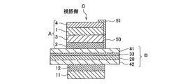
- the polarizing film A with an adhesive layer used on the visual side of the liquid crystal panel of the present invention has a first polarizing film 1, an anchor layer 3, and a first adhesive layer 2 in this order. Further, the polarizing film A with an adhesive layer may have a surface treatment layer 4 on the visible side of the first polarizing film 1.
- FIG. 1 illustrates a case where the surface treatment layer 4, the first polarizing film 1, the anchor layer 3, and the first pressure-sensitive adhesive layer 2 are provided in this order.
- a separator can be provided in the first pressure-sensitive adhesive layer 2 of the polarizing film A with a pressure-sensitive adhesive layer of the present invention, and a surface protective film is provided in the surface treatment layer 4. Can be done.
- the first polarizing film 1 a film having a protective film on one side or both sides of the polarizer is used, but from the viewpoint of optical durability, it is more than a single protective polarizing film having a protective film on only one side of the polarizer. It is preferable to use both protective polarizing films having protective films on both sides (no drawing).
- FIG. 2 shows a state of dimensional change before and after shrinkage in the film surface direction before and after charging when the polarizing film A with an adhesive layer was charged in an environment of 105 ° C. for 500 hours to perform a dimensional shrinkage test.
- This is an example of a conceptual diagram in a plan view.
- the polarizing film A with an adhesive layer before charging and the polarizing film A'with a pressure-sensitive adhesive layer shrunk after charging are shown.
- the amount of dimensional change of the polarizing film A with an adhesive layer is a distance between a predetermined point on the side surface of the polarizing film A with an adhesive layer and a side surface of the polarizing film A ′ with an adhesive layer and a predetermined point.
- At least a conductive structure is provided at the point b where the amount of dimensional change is 400 ⁇ m or less.
- the amount of dimensional change is preferably 350 ⁇ m or less, more preferably 300 ⁇ m or less, further preferably 250 ⁇ m or less, and further preferably 200 ⁇ m or less.
- point b will be described with respect to the relationship between the absorption axis direction and the direction orthogonal to the absorption axis (slow phase axis direction).
- the distance between the point b1 on the side surface in the same direction in the absorption axis direction and the point b1'of the polarizing film A'with an adhesive layer (dimension change amount in the slow axis direction).
- the dimensional change amount of 400 ⁇ m or less is satisfied.
- the dimensional change amount of 400 ⁇ m or less is satisfied for the point b1, it is considered that the dimensional change amount of 400 ⁇ m or less is satisfied at each point of the side b.
- the point b2'on the side surface of the curve connecting the side surfaces in the absorption axis direction and the slow phase axis direction for the deformed object having the rectangular corners processed.
- the distance between the image and the point b2'of the polarizing film A'with an adhesive layer is exemplified as a case where the amount of dimensional change satisfies 400 ⁇ m or less.
- the distance (the amount of dimensional change in the absorption axis direction) between the point a on the side surface in the slow axis direction and the point a of the polarizing film A'with an adhesive layer It is exemplified as a case where the dimensional change amount of 400 ⁇ m or less is not satisfied.
- the polarizing film A with the pressure-sensitive adhesive layer of FIG. 3 if the dimensional change amount of 400 ⁇ m or less is satisfied at the point a, it is considered that the dimensional change amount of 400 ⁇ m or less is not satisfied at each point of the side a.
- the ratio (b / a) of the dimensional change amount b ( ⁇ m) at the point b and the dimensional change amount a ( ⁇ m) in the absorption axis direction is 0. Satisfying the range of less than 8.8 is preferable from the viewpoint of maintaining the adhesion with the conductive structure provided on the side surface.
- the ratio (b / a) is preferably 0.7 or less, more preferably 0.6 or less.
- the size of the polarizing film (polarizing film A with an adhesive layer) used in the present invention is not particularly limited, but for example, a rectangular object having a length of 50 to 1500 mm and a width of 50 to 1500 mm is preferable.
- the polarizing film A with the pressure-sensitive adhesive layer allows the pressure-sensitive adhesive layer 2 to visually recognize the liquid crystal cell B (in-cell type liquid crystal cell B in FIGS. 4 to 8) as shown in FIG. It is arranged on the side of the first transparent substrate 41 on the side without a conductive layer. Further, the liquid crystal panel C has a conductive structure 50 on the side surface of the polarizing film A with an adhesive layer.
- the polarizing film A with an adhesive layer will be described below.
- the polarizing film A with an adhesive layer of the present invention has a first polarizing film, an anchor layer, and a first adhesive layer.
- the first polarizing film one having a polarizing element and a protective film on one side or both sides of the polarizing element is generally used.
- the polarizer is not particularly limited, and various polarizers can be used.
- the polarizer include a hydrophilic polymer film such as a polyvinyl alcohol-based film, a partially formalized polyvinyl alcohol-based film, and an ethylene-vinyl acetate copolymer system partially saponified film, which is uniaxially stretched by adsorbing iodine. Can be mentioned.
- a polarizer composed of a polyvinyl alcohol-based film and iodine is preferable.
- the thickness of these polarizers is not particularly limited, but is generally about 80 ⁇ m or less.
- a polarizing element having an iodine concentration of 6% by weight or less from the viewpoint of heat resistance.
- the iodine concentration is preferably 5% by weight or less, more preferably 4% by weight or less, from the viewpoint of heat resistance.
- the iodine concentration in the polarizer is preferably 1% by weight or more, more preferably 1.5% by weight or more, and further preferably 2% by weight or more. Is preferable.
- the iodine concentration of the polarizer is high, the amount of dimensional change is large, and the poor adhesion of the conductive structure due to heat shrinkage tends to cause poor conduction. Therefore, it is preferable to adjust the iodine concentration of the polarizer within the above range.
- a polarizing element having a thickness of more than 10 ⁇ m from the viewpoint of heat resistance.
- the thickness is preferably more than 10 ⁇ m to 25 ⁇ m, more preferably 10 to 22 ⁇ m, and further preferably 10 to 20 ⁇ m.
- the thicker the polarizer the larger the amount of dimensional change, and the insufficient adhesion of the conductive structure due to heat shrinkage tends to cause conduction failure. Therefore, it is preferable to adjust the thickness of the polarizing element within the above range.
- thermoplastic resin having excellent transparency, mechanical strength, thermal stability, moisture blocking property, isotropic property, etc.
- thermoplastic resins include cellulose resins such as triacetyl cellulose, polyester resins, polyether sulfone resins, polysulfone resins, polycarbonate resins, polyamide resins, polyimide resins, polyolefin resins, (meth) acrylic resins, and cyclic resins.
- examples thereof include polyolefin resins (norbornene-based resins), polyarylate resins, polystyrene resins, polyvinyl alcohol resins, and mixtures thereof.
- a protective film is attached to one side of the polarizer by an adhesive layer, but as a protective film on the other side, (meth) acrylic, urethane, acrylic urethane, epoxy, silicone, etc.
- Thermosetting resin or ultraviolet curable resin can be used.
- the protective film may contain one or more of any suitable additives.
- a cellulose resin and a (meth) acrylic resin are preferable because the fluctuation of the surface resistance value of the pressure-sensitive adhesive layer can be controlled to be small.
- the (meth) acrylic resin it is preferable to use a (meth) acrylic resin having a lactone ring structure.
- the (meth) acrylic resin having a lactone ring structure include JP-A-2000-230016, JP-A-2001-151814, JP-A-2002-120326, JP-A-2002-254544, JP-A-2005 Examples thereof include (meth) acrylic resins having a lactone ring structure described in Japanese Patent Application Laid-Open No. 146084.
- the cellulose resin is preferable to the (meth) acrylic resin in that it is effective in suppressing the polarizer crack, which is a problem in the single-protective polarizing film.
- a retardation film, a diffusion film, or the like can also be used.
- the retardation film include those having a frontal retardation of 40 nm or more and / or a thickness direction retardation of 80 nm or more.
- the front phase difference is usually controlled in the range of 40 to 200 nm
- the thickness direction phase difference is usually controlled in the range of 80 to 300 nm.
- the retardation film also functions as a polarizer protective film, so that the thickness can be reduced.
- the protective film and the polarizer are laminated via an intervening layer such as an adhesive layer, an adhesive layer, and an undercoat layer (primer layer). At this time, it is desirable that both are laminated without an air gap by an intervening layer.
- the protective film and the polarizer are preferably laminated via an adhesive layer.
- the adhesive used for bonding the polarizer and the protective film is not particularly limited as long as it is optically transparent, and various forms such as water-based, solvent-based, hot-melt-based, radical-curing type, and cation-curing type are used. However, water-based adhesives or radical curable adhesives are suitable.
- the first pressure-sensitive adhesive layer is formed of a pressure-sensitive adhesive composition containing a (meth) acrylic polymer (A) and an antistatic agent (B).
- the (meth) acrylic polymer (A) contains an alkyl (meth) acrylate as a main component as a monomer unit.
- (meth) acrylate means acrylate and / or methacrylate, and has the same meaning as (meth) of the present invention.
- alkyl (meth) acrylate constituting the main skeleton of the (meth) acrylic polymer (A) include those having a linear or branched alkyl group having 1 to 18 carbon atoms.
- the alkyl group includes methyl group, ethyl group, propyl group, isopropyl group, butyl group, isobutyl group, amyl group, hexyl group, cyclohexyl group, heptyl group, 2-ethylhexyl group, isooctyl group, nonyl group and decyl.
- Examples thereof include a group, an isodecyl group, a dodecyl group, an isomyristyl group, a lauryl group, a tridecyl group, a pentadecyl group, a hexadecyl group, a heptadecyl group, an octadecyl group and the like. These can be used alone or in combination.
- the average carbon number of these alkyl groups is preferably 3 to 9.
- the weight ratio of the alkyl (meth) acrylate is preferably 70% by weight or more in terms of the weight ratio of all the constituent monomers (100% by weight) constituting the (meth) acrylic polymer (A) as a monomer unit.
- the weight ratio of the alkyl (meth) acrylate can be considered as the balance of the other copolymerized monomers. It is preferable to set the weight ratio of the alkyl (meth) acrylate in the above range in order to ensure adhesiveness.
- (meth) acrylic polymer (A) in addition to the above-mentioned alkyl (meth) acrylate monomer unit, unsaturated (meth) acryloyl group, vinyl group, etc. are used for the purpose of improving adhesiveness and heat resistance.
- One or more types of copolymerizable monomers having a polymerizable functional group having a double bond can be introduced by copolymerization.
- copolymerization monomer examples include functional group-containing monomers such as a carboxyl group-containing monomer, a hydroxyl group-containing monomer, and an amide group-containing monomer.
- the carboxyl group-containing monomer is a compound containing a carboxyl group in its structure and containing a polymerizable unsaturated double bond such as a (meth) acryloyl group and a vinyl group.
- Specific examples of the carboxyl group-containing monomer include (meth) acrylic acid, carboxyethyl (meth) acrylate, carboxypentyl (meth) acrylate, itaconic acid, maleic acid, fumaric acid, crotonic acid and the like.
- acrylic acid is preferable from the viewpoint of copolymerizability, price, and adhesive properties.
- the hydroxyl group-containing monomer is a compound containing a hydroxyl group in its structure and containing a polymerizable unsaturated double bond such as a (meth) acryloyl group or a vinyl group.
- a polymerizable unsaturated double bond such as a (meth) acryloyl group or a vinyl group.
- Specific examples of the hydroxyl group-containing monomer include 2-hydroxyethyl (meth) acrylate, 3-hydroxypropyl (meth) acrylate, 4-hydroxybutyl (meth) acrylate, 6-hydroxyhexyl (meth) acrylate, and 8-hydroxyhexyl (meth) acrylate.
- hydroxyalkyl (meth) acrylates such as hydroxyoctyl (meth) acrylates, 10-hydroxydecyl (meth) acrylates and 12-hydroxylauryl (meth) acrylates, and (4-hydroxymethylcyclohexyl) -methyl acrylates.
- hydroxyl group-containing monomers 2-hydroxyethyl (meth) acrylate and 4-hydroxybutyl (meth) acrylate are preferable, and 4-hydroxybutyl (meth) acrylate is particularly preferable, from the viewpoint of durability.
- the carboxyl group-containing monomer and the hydroxyl group-containing monomer serve as reaction points with the cross-linking agent when the pressure-sensitive adhesive composition contains the cross-linking agent. Since the carboxyl group-containing monomer and the hydroxyl group-containing monomer are highly reactive with the intermolecular cross-linking agent, they are preferably used for improving the cohesiveness and heat resistance of the obtained first pressure-sensitive adhesive layer. Further, the carboxyl group-containing monomer is preferable in terms of achieving both durability and reworkability, and the hydroxyl group-containing monomer is preferable in terms of reworkability.
- the weight ratio of the carboxyl group-containing monomer is preferably 10% by weight or less, more preferably 0.01 to 8% by weight, further preferably 0.05 to 6% by weight, and further preferably 0.1 to 0.1% by weight. 5% by weight is preferable. It is preferable that the weight ratio of the carboxyl group-containing monomer is 0.01% by weight or more from the viewpoint of durability. On the other hand, if it exceeds 10% by weight, it is not preferable from the viewpoint of reworkability.
- the weight ratio of the hydroxyl group-containing monomer is preferably 3% by weight or less, more preferably 0.01 to 3% by weight, further preferably 0.1 to 2% by weight, and further 0.2 to 0.2 to 2% by weight. 2% by weight is preferable. It is preferable that the weight ratio of the hydroxyl group-containing monomer is 0.01% by weight or more from the viewpoint of cross-linking the first pressure-sensitive adhesive layer, durability and adhesive properties. On the other hand, if it exceeds 3% by weight, it is not preferable from the viewpoint of durability.
- the amide group-containing monomer is a compound containing an amide group in its structure and containing a polymerizable unsaturated double bond such as a (meth) acryloyl group and a vinyl group.
- Specific examples of the amide group-containing monomer include (meth) acrylamide, N, N-dimethyl (meth) acrylamide, N, N-diethyl (meth) acrylamide, N-isopropylacrylamide, N-methyl (meth) acrylamide, and N-.
- the amide group-containing monomer is preferable in order to suppress an increase in the surface resistance value over time (particularly in a humid environment) and to satisfy the durability.
- the N-vinyl group-containing lactam-based monomer suppresses an increase in the surface resistance value over time (particularly in a humid environment), and is a transparent conductive layer (touch sensor layer). It is preferable in terms of satisfying the durability against.
- the weight ratio of the amide group-containing monomer increases, the anchoring property with respect to the optical film tends to decrease. Therefore, the weight ratio is preferably 10% by weight or less, more preferably 5% by weight or less. Especially preferable.
- the weight ratio of the amide group-containing monomer is preferably 0.1% by weight or more from the viewpoint of suppressing an increase in the surface resistance value over time (particularly in a humid environment).
- the weight ratio is preferably 0.3% by weight or more, more preferably 0.5% by weight or more.
- the amide group is said to be present.
- the presence of the amide group suppresses the fluctuation and increase of the surface resistance value of the first pressure-sensitive adhesive layer adjusted by blending an antistatic agent (for example, ionic compound (B)) even in a humid environment. It is preferable to maintain the value within a desired range.
- the phase of the (meth) acrylic polymer (A) and the ionic compound (B) due to the presence of an amide group introduced as a functional group of the copolymerization monomer in the side chain of the (meth) acrylic polymer (A). It is thought that the solubility will increase.
- the first pressure-sensitive adhesive layer is a glass and a transparent conductive layer (ITO layer) when an amide group introduced into the side chain of the (meth) acrylic polymer (A) which is the base polymer is present. Etc.), and the durability is good, and it is possible to suppress the occurrence of peeling, floating, etc. in the state of being attached to the liquid crystal panel. Further, the durability can be satisfied even in a humidified environment (after the humidification reliability test).
- ITO layer transparent conductive layer
- an aromatic ring-containing (meth) acrylate As the copolymerization monomer, for example, an aromatic ring-containing (meth) acrylate can be used.
- An aromatic ring-containing (meth) acrylate is a compound having an aromatic ring structure in its structure and containing a (meth) acryloyl group. Examples of the aromatic ring include a benzene ring, a naphthalene ring, and a biphenyl ring.
- aromatic ring-containing (meth) acrylate examples include, for example, benzyl (meth) acrylate, phenyl (meth) acrylate, o-phenylphenol (meth) acrylate phenoxy (meth) acrylate, phenoxyethyl (meth) acrylate, and phenoxypropyl.
- benzene ring such as acrylate, methoxybenzyl (meth) acrylate, chlorobenzyl (meth) acrylate, cresyl (meth) acrylate, polystyryl (meth) acrylate; hydroxyethylated ⁇ -naphthol acrylate, 2-naphthoethyl (meth) acrylate , 2-naphthoxyethyl acrylate, 2- (4-methoxy-1-naphthoxy) ethyl (meth) acrylate or the like having a naphthalene ring; examples thereof include
- aromatic ring-containing (meth) acrylate benzyl (meth) acrylate and phenoxyethyl (meth) acrylate are preferable, and phenoxyethyl (meth) acrylate is particularly preferable, from the viewpoint of adhesive properties and durability.
- the weight ratio of the aromatic ring-containing (meth) acrylate is preferably 25% by weight or less, more preferably 3 to 25% by weight, further preferably 10 to 22% by weight, and further preferably 14 to 20% by weight. Is preferable.
- the weight ratio of the aromatic ring-containing (meth) acrylate is 3% by weight or more, it is preferable in order to suppress display unevenness. On the other hand, if it exceeds 25% by weight, the display unevenness is not sufficiently suppressed, and the durability tends to decrease.
- copolymerization monomers other than the above include; acid anhydride group-containing monomers such as maleic anhydride and itaconic anhydride; caprolactone adducts of acrylic acid; allylsulfonic acid, 2- (meth) acrylamide-2. -Sulfonic acid group-containing monomers such as methylpropanesulfonic acid, (meth) acrylamide propanesulfonic acid, sulfopropyl (meth) acrylate; and phosphoric acid group-containing monomers such as 2-hydroxyethylacryloyl phosphate.
- acid anhydride group-containing monomers such as maleic anhydride and itaconic anhydride
- caprolactone adducts of acrylic acid allylsulfonic acid, 2- (meth) acrylamide-2.
- -Sulfonic acid group-containing monomers such as methylpropanesulfonic acid, (meth) acrylamide propanesulfonic acid, sulfo
- alkylaminoalkyl (meth) acrylates such as aminoethyl (meth) acrylate, N, N-dimethylaminoethyl (meth) acrylate, and t-butylaminoethyl (meth) acrylate; methoxyethyl (meth) acrylate, ethoxyethyl ( Alkoxyalkyl (meth) acrylates such as meta) acrylates; N- (meth) acryloyloxymethylene succinimide, N- (meth) acryloyl-6-oxyhexamethylene succinimide, N- (meth) acryloyl-8-oxyoctamethylene succinimide, etc.
- Succinimide-based monomers such as N-cyclohexyl maleimide, N-isopropyl maleimide, N-lauryl maleimide and N-phenylmaleimide; N-methylitaconimide, N-ethylitaconimide, N-butylitaconimide, N- Itaconimide-based monomers such as octylitaconimide, N-2-ethylhexylitaconimide, N-cyclohexylitaconimide, and N-laurylitaconimide are also mentioned as examples of monomers for modification purposes.
- a vinyl-based monomer such as vinyl acetate and vinyl propionate; a cyanoacrylate-based monomer such as acrylonitrile and methacrylonitrile; an epoxy group-containing (meth) acrylate such as glycidyl (meth) acrylate; and polyethylene glycol (meth).
- Glycol-based (meth) acrylates such as acrylates, polypropylene glycol (meth) acrylates, methoxyethylene glycol (meth) acrylates, and methoxypolypropylene glycol (meth) acrylates; tetrahydrofurfuryl (meth) acrylates, fluorine (meth) acrylates, silicones (meth).
- (Meta) acrylate monomers such as acrylate and 2-methoxyethyl acrylate can also be used. Further, isoprene, butadiene, isobutylene, vinyl ether and the like can be mentioned.
- examples of copolymerizable monomers other than the above include silane-based monomers containing a silicon atom.
- examples of the silane-based monomer include 3-acryloxypropyltriethoxysilane, vinyltrimethoxysilane, vinyltriethoxysilane, 4-vinylbutyltrimethoxysilane, 4-vinylbutyltriethoxysilane, and 8-vinyloctyltrimethoxysilane.
- 8-Vinyloctyloxydecyltriethoxysilane 10-methacryloyloxydecyltrimethoxysilane, 10-acryloyloxydecyltrimethoxysilane, 10-methacryloyloxydecyltriethoxysilane, 10-acryloyloxydecyltriethoxysilane and the like.
- copolymerization monomer examples include tripropylene glycol di (meth) acrylate, tetraethylene glycol di (meth) acrylate, 1,6-hexanediol di (meth) acrylate, bisphenol A diglycidyl ether di (meth) acrylate, and neo.
- the proportion of the other copolymerized monomer in the (meth) acrylic polymer (A) is about 0 to 10% by weight based on the weight ratio of all the constituent monomers (100% by weight) of the (meth) acrylic polymer (A). Further, it is preferably about 0 to 7% by weight, more preferably about 0 to 5% by weight.
- the (meth) acrylic polymer (A) of the present invention usually preferably has a weight average molecular weight of 1 million to 2.5 million. Considering durability, particularly heat resistance, the weight average molecular weight is preferably 1.2 million to 2 million. When the weight average molecular weight is 1 million or more, it is preferable from the viewpoint of heat resistance. Further, when the weight average molecular weight is larger than 2.5 million, the adhesive tends to be hard and peeling is likely to occur.
- the weight average molecular weight (Mw) / number average molecular weight (Mn) which indicates the molecular weight distribution, is preferably 1.8 or more and 10 or less, more preferably 1.8 to 7, and further 1.8 to. It is preferably 5.
- the weight average molecular weight and the molecular weight distribution (Mw / Mn) are measured by GPC (gel permeation chromatography) and obtained from the values calculated by polystyrene conversion.
- the obtained (meth) acrylic polymer (A) may be any of a random copolymer, a block copolymer, a graft copolymer and the like.
- solution polymerization for example, ethyl acetate, toluene and the like are used as the polymerization solvent.
- the reaction is carried out under an inert gas stream such as nitrogen, a polymerization initiator is added, and usually at about 50 to 70 ° C. under reaction conditions of about 5 to 30 hours.
- the polymerization initiator, chain transfer agent, emulsifier, etc. used for radical polymerization are not particularly limited and can be appropriately selected and used.
- the weight average molecular weight of the (meth) acrylic polymer (A) can be controlled by the amount of the polymerization initiator and the chain transfer agent used, and the reaction conditions, and the amount used is appropriately adjusted according to these types. To.
- Antistatic agent examples include materials capable of imparting antistatic properties such as an ionic surfactant system, a conductive polymer, and conductive fine particles. Further, as the antistatic agent, an ionic compound can be used.
- ionic surfactants examples include cationic surfactants (for example, quaternary ammonium salt type, phosphonium salt type, sulfonium salt type, etc.) and anionic surfactants (carboxylic acid type, sulfonate type, sulfate type, phosphate type, phosphite type, etc.).
- Amphoteric ion type (sulfobetaine type, alkylbetaine type, alkylimidazolium betaine type, etc.) or nonionic type (polyhydric alcohol derivative, ⁇ -cyclodextrin inclusion compound, sorbitan fatty acid monoester diester, polyalkylene oxide derivative, amine
- nonionic type polyhydric alcohol derivative, ⁇ -cyclodextrin inclusion compound, sorbitan fatty acid monoester diester, polyalkylene oxide derivative, amine
- surfactants such as oxides
- the conductive polymer examples include polyaniline-based, polythiophene-based, polypyrrole-based, and polyquinoxaline-based polymers.
- polyaniline and polythiophene which tend to be water-soluble conductive polymers or water-dispersible conductive polymers, are used. Etc. are preferably used.
- Polythiophene is particularly preferred.
- Examples of the conductive fine particles include metal oxides such as tin oxide, antimony oxide, indium oxide, and zinc oxide. Of these, tin oxide is preferable.
- Examples of tin oxide-based materials include tin oxide, antimony-doped tin oxide, indium-doped tin oxide, aluminum-doped tin oxide, tungsten-doped tin oxide, titanium oxide-cerium oxide-tin oxide complex, and titanium oxide-. Examples thereof include a complex of tin oxide.
- the average particle size of the fine particles is about 1 to 100 nm, preferably 2 to 50 nm.
- antistatic agents other than the above, acetylene black, ketjen black, natural graphite, artificial graphite, titanium black, cationic type (quaternary ammonium salt, etc.), amphoteric ion type (betaine compound, etc.), anionic type (sulfonic acid)
- a polymer having ionic conductivity such as a polymer having a site of origin; a permanent antistatic agent of a type in which a hydrophilic polymer such as a polyethylene methacrylate copolymer is alloyed with an acrylic resin or the like can be exemplified.
- the antistatic agent used for forming the first pressure-sensitive adhesive layer it is preferable to use an ionic compound among the above examples.
- an ionic compound an ionic liquid is preferable from the viewpoint of antistatic function.
- an alkali metal salt and / or an organic cation-anionic salt can be preferably used.
- organic salts and inorganic salts of alkali metals can be used.
- the term "organic cation-anionic salt” as used in the present invention refers to an organic salt whose cation portion is composed of an organic substance, and the anion portion may be an organic substance or an inorganic substance. There may be.
- the "organic cation-anionic salt” is also referred to as an ionic liquid or an ionic solid.
- alkali metal ions constituting the cation portion of the alkali metal salt include lithium, sodium, and potassium ions. Among these alkali metal ions, lithium ions are preferable.
- the anionic portion of the alkali metal salt may be composed of an organic substance or an inorganic substance.
- the anion portion constituting the organic salt include CH 3 COO ⁇ , CF 3 COO ⁇ , CH 3 SO 3 ⁇ , CF 3 SO 3 ⁇ , (CF 3 SO 2 ) 3 C ⁇ , C 4 F 9 SO 3 -, C 3 F 7 COO - , (CF 3 SO 2) (CF 3 CO) N -, (FSO 2) 2 N-, - O 3 S (CF 2) 3 SO 3 -, PF 6 -, CO 3 2- , and the following general formulas (1) to (4), (1) :( C n F 2n + 1 SO 2) 2 N - ( where, n is an integer of 0 to 10), (2): CF 2 (C m F 2m SO 2) 2 N - ( where, m is an integer of from 1 to 10), (3): - O 3 S (CF 2) l SO 3 - ( where, l is an integer of from 1 to 10
- the anion portion containing a fluorine atom is preferably used because an ionic compound having good ionic dissociation property can be obtained.
- the anion portion constituting the inorganic salts, Cl -, Br -, I -, AlCl 4 -, Al 2 Cl 7 -, BF 4 -, PF 6 -, ClO 4 -, NO 3 -, AsF 6 -, SbF 6 -, NbF 6 -, TaF 6 -, (CN) 2 N -, and the like can be used.
- anionic portion (CF 3 SO 2) 2 N -, (C 2 F 5 SO 2) 2 N -, wherein represented by formula (1) etc., (perfluoroalkyl sulfonyl) imide are preferable, especially ( A (trifluoromethanesulfonyl) imide represented by CF 3 SO 2 ) 2 N ⁇ is preferred.
- organic salt of the alkali metal examples include sodium acetate, sodium alginate, sodium lignin sulfonate, sodium toluene sulfonate, LiCF 3 SO 3 , Li (CF 3 SO 2 ) 2 N, and Li (CF 3 SO 2).
- Inorganic salts of alkali metals include lithium perchlorate and lithium iodide.
- the organic cation-anion salt used in the present invention is composed of a cation component and an anion component, and the cation component is composed of an organic substance.
- the cation component include pyridinium cation, piperidinium cation, pyrrolidinium cation, cation having a pyrroline skeleton, cation having a pyrrole skeleton, imidazolium cation, tetrahydropyrimidinium cation, and dihydropyrimidinium cation.
- Examples thereof include pyrazolium cation, pyrazolinium cation, tetraalkylammonium cation, trialkylsulfonium cation, tetraalkylphosphonium cation and the like.
- the anionic component e.g., Cl -, Br -, I -, AlCl 4 -, Al 2 Cl 7 -, BF 4 -, PF 6 -, ClO 4 -, NO 3 -, CH 3 COO -, CF 3 COO -, CH 3 SO 3 -, CF 3 SO 3 -, (CF 3 SO 2) 3 C -, AsF 6 -, SbF 6 -, NbF 6 -, TaF 6 -, (CN) 2 N -, C 4 F 9 SO 3 -, C 3 F 7 COO -, ((CF 3 SO 2) (CF 3 CO) N -, (FSO 2) 2 N-, - O 3 S (CF 2) 3 SO 3 -, and the following General formulas (1) to (4), (1) :( C n F 2n + 1 SO 2) 2 N - ( where, n is an integer of 0 to 10), (2): CF 2 (C m F 2m SO 2) 2 N - ( where, m
- ionic compound examples include inorganic salts such as ammonium chloride, aluminum chloride, copper chloride, ferric chloride, ferric chloride and ammonium sulfate, in addition to the above-mentioned alkali metal salt and organic cation-anionic salt. .. These ionic compounds can be used alone or in combination of two or more.
- the ionic compound having a molecular weight of 210 or less is preferably 150 or less, further preferably 110 or less, further preferably 50 or less, and further preferably 10 or less.
- the larger the molecular weight of the cation component the more the (meth) acrylic polymers in the pressure-sensitive adhesive layer are prevented from being entangled with each other, and the physical properties of the pressure-sensitive adhesive layer tend to be softened.
- alkali metal salt alkali metal ions such as lithium, sodium, and potassium are cationic components having a molecular weight of 210 or less. Therefore, alkali metal salts containing these alkali metal ions as cationic components are preferable. Can be used for.
- an organic salt of an alkali metal in which the anionic component of the alkali metal salt is composed of an organic substance is preferable.
- the alkali metal ion lithium ion having the smallest molecular weight is preferable.
- a lithium salt is preferable, and an organic salt of lithium is particularly preferable.
- the ionic compound is an organic cation-anion salt
- a molecular weight of 210 or less can be selected and used from the above-exemplified cation components.
- an organic cation-anion salt in which the anionic component is composed of an organic substance is preferable.
- the amount of the pressure-sensitive adhesive and antistatic agent used is controlled so that the surface resistance value of the obtained first pressure-sensitive adhesive layer is 1 ⁇ 10 8 to 1 ⁇ 10 12 ⁇ / ⁇ , although it depends on their types.
- an antistatic agent for example, in the case of an ionic compound
- an antistatic agent in the range of 0.05 to 20 parts by weight with respect to 100 parts by weight of the (meth) acrylic polymer.
- an antistatic agent in an amount of 0.05 parts by weight or more in order to improve the antistatic performance.
- the antistatic agent (B) is preferably 0.1 part by weight or more, and more preferably 0.5 part by weight or more. In order to satisfy the durability, it is preferably used in an amount of 20 parts by weight or less, and more preferably 10 parts by weight or less.
- the proportion of the ionic compound (B) in the pressure-sensitive adhesive composition of the present invention can be appropriately adjusted so as to satisfy the antistatic properties of the first pressure-sensitive adhesive layer and the sensitivity of the touch panel.
- touch sensing while considering the type of protective film of the polarizing film so that the surface resistance value of the first pressure-sensitive adhesive layer is in the range of 1.0 ⁇ 10 8 to 1.0 ⁇ 10 12 ⁇ / ⁇ .
- the initial surface resistance value of the first adhesive layer is controlled in the range of 1 ⁇ 10 8 to 1 ⁇ 10 12 ⁇ / ⁇ . It is preferable to control the pressure in the range of 1 ⁇ 10 8 to 1 ⁇ 10 11 ⁇ / ⁇ .
- the pressure-sensitive adhesive composition of the present invention can contain a cross-linking agent (C).
- a cross-linking agent C
- an organic cross-linking agent or a polyfunctional metal chelate can be used.
- the organic cross-linking agent include isocyanate-based cross-linking agents, peroxide-based cross-linking agents, epoxy-based cross-linking agents, and imine-based cross-linking agents.
- a polyfunctional metal chelate is one in which a polyvalent metal is covalently or coordinated to an organic compound.
- Examples of the polyvalent metal atom include Al, Cr, Zr, Co, Cu, Fe, Ni, V, Zn, In, Ca, Mg, Mn, Y, Ce, Sr, Ba, Mo, La, Sn, Ti and the like. Can be mentioned.
- Examples of the atom in the organic compound having a covalent bond or a coordination bond include an oxygen atom and the like, and examples of the organic compound include an alkyl ester, an alcohol compound, a carboxylic acid compound, an ether compound and a ketone compound.
- cross-linking agent (C) an isocyanate-based cross-linking agent and / or a peroxide-based cross-linking agent is preferable.
- isocyanate-based cross-linking agent (C) a compound having at least two isocyanate groups can be used.
- known aliphatic polyisocyanates, alicyclic polyisocyanates, aromatic polyisocyanates, etc., which are generally used for urethanization reactions, are used.
- any peroxide that generates radically active species by heating or light irradiation to promote cross-linking of the base polymer of the pressure-sensitive adhesive composition can be appropriately used, but in consideration of workability and stability. It is preferable to use a peroxide having a half-life temperature of 80 ° C. to 160 ° C. for 1 minute, and more preferably to use a peroxide having a half-life temperature of 90 ° C. to 140 ° C.
- peroxide examples include di (2-ethylhexyl) peroxydicarbonate (1 minute half-life temperature: 90.6 ° C.) and di (4-t-butylcyclohexyl) peroxydicarbonate (1).
- the amount of the cross-linking agent (C) used is preferably 3 parts by weight or less, more preferably 0.01 to 3 parts by weight, and further 0.02 with respect to 100 parts by weight of the (meth) acrylic polymer (A). It is preferably from 2 parts by weight, more preferably 0.03 to 1 part by weight. If the amount of the cross-linking agent (C) is less than 0.01 parts by weight, the first pressure-sensitive adhesive layer may be insufficiently cross-linked and the durability and adhesive properties may not be satisfied. On the other hand, if the amount is more than 3 parts by weight, the first pressure-sensitive adhesive layer may not be satisfied. There is a tendency for the pressure-sensitive adhesive layer to become too hard and reduce its durability.
- the pressure-sensitive adhesive composition of the present invention can contain a silane coupling agent (D).
- Durability can be improved by using the silane coupling agent (D).
- Specific examples of the silane coupling agent include 3-glycidoxypropyltrimethoxysilane, 3-glycidoxypropyltriethoxysilane, 3-glycidoxypropylmethyldiethoxysilane, and 2- (3, 4-Epylcyclohexyl) Epyl group-containing silane coupling agent such as ethyltrimethoxysilane, 3-aminopropyltrimethoxysilane, N-2- (aminoethyl) -3-aminopropylmethyldimethoxysilane, 3-triethoxysilyl- Amino group-containing silane coupling agents such as N- (1,3-dimethylbutylidene) propylamine and N-phenyl- ⁇ -aminopropyltrimethoxysilane, 3-acryloxy
- Examples thereof include (meth) acrylic group-containing silane coupling agents such as ethoxysilane, and isocyanate group-containing silane coupling agents such as 3-isocyanuppropyltriethoxysilane.
- an epoxy group-containing silane coupling agent is preferable.
- silane coupling agent (D) one having a plurality of alkoxysilyl groups in the molecule can also be used.
- a silane coupling agent having a plurality of alkoxysilyl groups in these molecules is preferable because it is difficult to volatilize and has a plurality of alkoxysilyl groups, which is effective in improving durability.
- the adherend of the optical film with the pressure-sensitive adhesive layer is a transparent conductive layer (for example, ITO or the like) in which the alkoxysilyl group is less likely to react than glass.
- the silane coupling agent having a plurality of alkoxysilyl groups in the molecule preferably has an epoxy group in the molecule, and more preferably has a plurality of epoxy groups in the molecule.
- a silane coupling agent having a plurality of alkoxysilyl groups in the molecule and having an epoxy group tends to have good durability even when the adherend is a transparent conductive layer (for example, ITO).
- silane coupling agent having a plurality of alkoxysilyl groups in the molecule and having an epoxy group examples include X-41-1053, X-41-1059A, and X-41-1056 manufactured by Shin-Etsu Chemical Co., Ltd.
- X-41-1056 manufactured by Shin-Etsu Chemical Co., Ltd. which has a high epoxy group content, is preferable.
- the silane coupling agent (D) may be used alone or in combination of two or more, but the content as a whole is the (meth) acrylic polymer (A) 100. It is preferably 5 parts by weight or less, more preferably 0.001 to 5 parts by weight, further preferably 0.01 to 1 part by weight, still more preferably 0.02 to 1 part by weight, and further. Is preferably 0.05 to 0.6 parts by weight. It is an amount that improves durability.
- the pressure-sensitive adhesive composition of the present invention may contain other known additives, for example, a polyether compound having a reactive silyl group, a polyether compound of polyalkylene glycol such as polypropylene glycol, and coloring. Powders of agents, pigments, dyes, surfactants, plasticizers, tackifiers, surface lubricants, leveling agents, softeners, antioxidants, antioxidants, light stabilizers, UV absorbers, polymerization prohibited Agents, inorganic or organic fillers, metal powders, particles, foils and the like can be appropriately added depending on the intended use. Further, a redox system to which a reducing agent is added may be adopted within a controllable range. These additives are preferably used in a range of 5 parts by weight or less, further 3 parts by weight or less, and further 1 part by weight or less with respect to 100 parts by weight of the (meth) acrylic polymer (A).
- a polyether compound having a reactive silyl group such as polypropylene glycol
- the pressure-sensitive adhesive composition is applied to a peel-treated separator or the like, and a polymerization solvent or the like is dried and removed to form the first pressure-sensitive adhesive layer, and then an optical film (polarization) is formed. It is produced by a method of transferring to a film), or a method of applying the pressure-sensitive adhesive composition to an optical film (polarizing film) and drying and removing a polymerization solvent or the like to form a first pressure-sensitive adhesive layer on the optical film.
- one or more solvents other than the polymerization solvent may be newly added as appropriate.
- the thickness of the first pressure-sensitive adhesive layer is not particularly limited, and is, for example, about 1 to 100 ⁇ m. It is preferably 2 to 50 ⁇ m, more preferably 2 to 40 ⁇ m, and even more preferably 5 to 35 ⁇ m.
- the thickness of the first pressure-sensitive adhesive layer 2 is preferably 5 to 100 ⁇ m, preferably 5 to 50 ⁇ m, and further 10 to 35 ⁇ m from the viewpoint of ensuring durability and securing a contact area with the conductive structure on the side surface. Is preferable.
- the anchor layer can be formed of various materials.
- the thickness of the anchor layer is preferably 0.01 to 0.5 ⁇ m, preferably 0.01 to 0.2 ⁇ m, and further preferably 0.01 to 0.1 ⁇ m.
- the anchor layer contains a conductive polymer and has conductivity.
- the surface resistance value is preferably 1 ⁇ 10 6 to 1 ⁇ 10 9 ⁇ / ⁇ from the viewpoint of the antistatic function.
- the conductive polymer is preferably used from the viewpoint of optical properties, appearance, antistatic effect, and stability of the antistatic effect during heat and humidification.
- conductive polymers such as polyaniline and polythiophene are preferably used.
- an organic solvent-soluble, water-soluble, or water-dispersible polymer can be appropriately used, but a water-soluble conductive polymer or a water-dispersible conductive polymer is preferably used.
- the water-soluble conductive polymer and the water-dispersible conductive polymer can be prepared as an aqueous solution or an aqueous dispersion as a coating liquid for forming an antistatic layer, and the coating liquid does not need to use a non-aqueous organic solvent and is organic.
- the aqueous solution or the aqueous dispersion can contain an aqueous solvent in addition to water.
- an aqueous solvent for example, methanol, ethanol, n-propanol, isopropanol, n-butanol, isobutanol, sec-butanol, tert-butanol, n-amyl alcohol, isoamyl alcohol, sec-amyl alcohol, tert-amyl alcohol, 1-ethyl-1.
- -Alcohols such as propanol, 2-methyl-1-butanol, n-hexanol, cyclohexanol and the like can be mentioned.
- the water-soluble conductive polymer such as polyaniline and polythiophene or the water-dispersible conductive polymer preferably has a hydrophilic functional group in the molecule.
- the hydrophilic functional group include a sulfon group, an amino group, an amide group, an imino group, a quaternary ammonium base, a hydroxyl group, a mercapto group, a hydrazino group, a carboxyl group, a sulfate ester group, a phosphoric acid ester group, or a salt thereof. And so on.
- a hydrophilic functional group in the molecule it becomes easy to be dissolved in water or dispersed in water in the form of fine particles, and the water-soluble conductive polymer or the water-dispersible conductive polymer can be easily prepared.
- Examples of commercially available water-soluble conductive polymers include polyaniline sulfonic acid (manufactured by Mitsubishi Rayon Co., Ltd., weight average molecular weight of 150,000 in terms of polystyrene).
- Examples of commercially available water-dispersible conductive polymers include polythiophene-based conductive polymers (manufactured by Nagase Chemtech, trade name, Denatron series).
- a binder component can be added together with the antistatic agent for the purpose of improving the film-forming property of the antistatic agent and the adhesion to the optical film.
- the antistatic agent is a water-soluble conductive polymer or a water-based material of the water-dispersible conductive polymer
- a water-soluble or water-dispersible binder component is used.
- binders include oxazoline group-containing polymers, polyurethane resins, polyester resins, acrylic resins, polyether resins, cellulose resins, polyvinyl alcohol resins, epoxy resins, polyvinylpyrrolidone, polystyrene resins, polyethylene glycol, etc. Examples include pentaerythritol.
- polyurethane-based resins, polyester-based resins, and acrylic-based resins are preferable.
- One or two or more of these binders can be appropriately used according to the intended use.
- the amount of the antistatic agent and the binder used depends on their types, but it is preferable to control the surface resistance value of the obtained anchor layer to be 1 ⁇ 10 6 to 1 ⁇ 10 9 ⁇ / ⁇ .
- a functional layer such as a hard coat layer, an antiglare treatment layer, an antireflection layer, an antisticking layer or an antiglare layer can be provided.
- the surface treatment layer can be provided on a surface of the protective film to which the polarizer is not adhered.
- the surface resistance value of the surface treatment layer 4 is 1 ⁇ 10 6 to 1 ⁇ 10 11 ⁇ / ⁇ from the viewpoint of antistatic function and touch sensor sensitivity. It is preferably 1 ⁇ 10 6 to 1 ⁇ 10 10 ⁇ / ⁇ , and more preferably 1 ⁇ 10 6 to 1 ⁇ 10 9 ⁇ .
- the surface treatment layer When imparting conductivity to the surface treatment layer, the surface treatment layer is preferably formed so that the surface resistance value is 1 ⁇ 10 6 to 1 ⁇ 10 11 ⁇ / ⁇ .
- Conductivity can be imparted to the surface treatment layer by containing an antistatic agent.
- the surface treatment layer can be provided on the protective film used for the first polarizing film, or can be provided separately from the protective film.
- the antistatic agent used to impart conductivity to the surface treatment layer those exemplified above can be used, but at least one selected from an ionic surfactant, conductive fine particles and a conductive polymer. It is preferable to contain one type.
- the antistatic agent used for the surface treatment layer is preferably conductive fine particles from the viewpoint of optical characteristics, appearance, antistatic effect, and stability of the antistatic effect during heat and humidification.
- the surface treatment layer is preferably a hard coat layer.
- a thermoplastic resin or a material that is cured by heat or radiation can be used as the material for forming the hard coat layer.
- the material include radiation-curable resins such as thermosetting resins, ultraviolet curable resins, and electron beam curable resins.
- an ultraviolet curable resin that can efficiently form a cured resin layer by a simple processing operation by a curing treatment by ultraviolet irradiation is preferable.
- these curable resins include various types such as polyester-based, acrylic-based, urethane-based, amide-based, silicone-based, epoxy-based, and melamine-based resins, and include these monomers, oligomers, and polymers.
- a radiation-curable resin particularly an ultraviolet-curable resin
- the ultraviolet curable resin preferably used include those having an ultraviolet polymerizable functional group, and among them, those containing an acrylic monomer or an oligomer component having 2 or more, particularly 3 to 6 of the functional groups. Further, the ultraviolet curable resin contains a photopolymerization initiator.
- an antiglare treatment layer or an antireflection layer for the purpose of improving visibility can be provided.
- an antiglare treatment layer and an antireflection layer can be provided on the hard coat layer.
- the constituent material of the antiglare treatment layer is not particularly limited, and for example, a radiation-curable resin, a thermosetting resin, a thermoplastic resin, or the like can be used.
- As the antireflection layer titanium oxide, zirconium oxide, silicon oxide, magnesium fluoride and the like are used.
- a plurality of antireflection layers can be provided.
- examples of the surface treatment layer include a sticking prevention layer and the like.
- the thickness of the surface treatment layer can be appropriately set depending on the type of the surface treatment layer, but is generally preferably 0.1 to 100 ⁇ m.
- the thickness of the hard coat layer is preferably 0.5 to 20 ⁇ m.
- the thickness of the hard coat layer is not particularly limited, but if it is too thin, sufficient hardness as a hard coat layer cannot be obtained, while if it is too thick, cracks and peeling are likely to occur.
- the thickness of the hard coat layer is more preferably 1 to 10 ⁇ m.
- the amount of antistatic agent and binder (resin material, etc.) used in the surface treatment layer depends on their types, but the surface resistance value of the obtained surface treatment layer is 1 ⁇ 10 7 to 1 ⁇ 10 11 ⁇ / It is preferable to control so as to be ⁇ .
- the amount of the binder is 1000 parts by weight or less, more preferably 10 to 200 parts by weight, based on 100 parts by weight of the antistatic agent.
- an easy-adhesive layer is provided on the surface of the first polarizing film on the side where the anchor layer is provided, and various easy-adhesion such as corona treatment and plasma treatment are performed. It can be processed.
- liquid crystal cell B and the liquid crystal panel C will be described below.
- the liquid crystal cell B includes a liquid crystal layer 20 containing liquid crystal molecules homogenically oriented in the absence of an electric field, a first transparent substrate 41 and a second transparent substrate 42 sandwiching the liquid crystal layer 20 on both sides. Have. In FIG. 3, the electrodes in the liquid crystal cell B are omitted.
- liquid crystal layer 20 used in the liquid crystal cell B a liquid crystal layer containing liquid crystal molecules homogenically oriented in the absence of an electric field is used.
- liquid crystal layer 20 for example, an IPS type liquid crystal layer is preferably used.
- any type of liquid crystal layer such as TN type, STN type, ⁇ type, or VA type can be used.
- the thickness of the liquid crystal layer 20 is, for example, about 1.5 ⁇ m to 4 ⁇ m.
- Examples of the material for forming the transparent substrate include glass or a polymer film.
- Examples of the polymer film include polyethylene terephthalate, polycycloolefin, polycarbonate and the like.
- When the transparent substrate is made of glass its thickness is, for example, about 0.1 mm to 1 mm.
- the transparent substrate may have an easy-adhesion layer or a hard coat layer on its surface.
- the in-cell liquid crystal cell B As the liquid crystal cell B, the in-cell type liquid crystal cell B shown in FIGS. 4 to 8 can be used.
- the in-cell liquid crystal cell B also has a touch sensor and a touch sensing electrode portion related to a touch drive function between the first transparent substrate 41 and the second transparent substrate 42.
- the touch sensing electrode portion can be formed by the touch sensor electrode 31 and the touch drive electrode 32.
- the touch sensor electrode referred to here refers to a touch detection (reception) electrode.
- the touch sensor electrode 31 and the touch drive electrode 32 can be independently formed by various patterns. For example, when the in-cell type liquid crystal cell B is a flat surface, it can be arranged in a pattern that intersects at a right angle by a form provided independently in the X-axis direction and the Y-axis direction, respectively. Further, in FIGS. 4, 5, and 8, the touch sensor electrode 31 is arranged on the side (visual side) of the first transparent substrate 41 with respect to the touch drive electrode 32, but the opposite is true.
- the touch drive electrode 32 may be arranged closer to the first transparent substrate 41 (visual recognition side) than the touch sensor electrode 31.
- an electrode 33 in which a touch sensor electrode and a touch drive electrode are integrally formed can be used.
- the touch sensing electrode portion can be arranged between the liquid crystal layer 20 and the first transparent substrate 41 or the second transparent substrate 42.
- 4 and 6 show a case where the touch sensing electrode portion is arranged between the liquid crystal layer 20 and the first transparent substrate 41 (on the visual side of the liquid crystal layer 20).
- 5 and 7 show a case where the touch sensing electrode portion is arranged between the liquid crystal layer 20 and the second transparent substrate 42 (on the backlight side of the liquid crystal layer 20).
- the touch sensing electrode portion has a touch sensor electrode 31 between the liquid crystal layer 20 and the first transparent substrate 41, and the liquid crystal layer 20 and the second transparent substrate 42 A touch drive electrode 32 may be provided between them.
- the drive electrode (the electrode 33 in which the touch drive electrode 32, the touch sensor electrode, and the touch drive electrode are integrally formed) in the touch sensing electrode portion can also be used as a common electrode for controlling the liquid crystal layer 20.
- the in-cell type liquid crystal cell B has a touch sensor and a touch sensing electrode portion related to the touch drive function in the liquid crystal cell, and does not have a touch sensor electrode outside the liquid crystal cell. That is, the conductive layer (surface resistance value is 1 ⁇ 10 13 ⁇ /) is on the visible side of the in-cell liquid crystal cell B from the first transparent substrate 41 (on the liquid crystal cell side of the first adhesive layer 2 of the in-cell liquid crystal panel C). ⁇ Below) is not provided.
- the in-cell liquid crystal panel C shown in FIGS. 4 to 8 shows the order of each configuration, the in-cell liquid crystal panel C may have other configurations as appropriate.
- a color filter substrate can be provided on the liquid crystal cell (first transparent substrate 41).
- the touch sensor electrode 31 (capacitance sensor), the touch drive electrode 32, or the electrode 33 in which the touch sensor electrode and the touch drive electrode are integrally formed, which form the touch sensing electrode portion, are formed as a transparent conductive layer.
- the constituent material of the transparent conductive layer is not particularly limited, and for example, metals such as gold, silver, copper, platinum, palladium, aluminum, nickel, chromium, titanium, iron, cobalt, tin, magnesium, and tungsten, and metals such as these metals. Examples include alloys.
- Examples of the constituent material of the transparent conductive layer include metal oxides of indium, tin, zinc, gallium, antimony, zirconium, and cadmium, and specifically, indium oxide, tin oxide, titanium oxide, cadmium oxide, and these. Examples thereof include metal oxides composed of a mixture of the above. In addition, other metal compounds such as copper iodide are used. The metal oxide may further contain oxides of the metal atoms shown in the above group, if necessary. For example, indium oxide (ITO) containing tin oxide, tin oxide containing antimony, and the like are preferably used, and ITO is particularly preferably used. The ITO preferably contains 80 to 99% by weight of indium oxide and 1 to 20% by weight of tin oxide.
- ITO indium oxide
- the electrodes (touch sensor electrode 31, touch drive electrode 32, touch sensor electrode, and touch drive electrode 33 integrally formed) related to the touch sensing electrode portion are usually the first transparent substrate 41 and / or the second transparent electrode. It can be formed as a transparent electrode pattern on the inside of the substrate 42 (on the liquid crystal layer 20 side in the in-cell type liquid crystal cell B) by a conventional method.
- the transparent electrode pattern is usually electrically connected to a routing wire (not shown) formed at the end of the transparent substrate, and the routing wire is connected to a controller IC (not shown).
- a routing wire not shown
- any shape such as a stripe shape or a rhombus shape can be adopted depending on the application.
- the height of the transparent electrode pattern is, for example, 10 nm to 100 nm, and the width is 0.1 mm to 5 mm.
- the liquid crystal panel C of the present invention may have the polarizing film A with an adhesive layer on the visible side of the liquid crystal cell B and the second polarizing film 11 on the opposite side.
- FIGS. 4 to 8 show an in-cell type liquid crystal panel using the in-cell type liquid crystal cell B.
- the polarizing film A with an adhesive layer is arranged on the side of the first transparent substrate 41 of the liquid crystal cell B via the first adhesive layer 2 without interposing a conductive layer.
- the second polarizing film 11 is arranged on the side of the second transparent substrate 42 of the liquid crystal cell B via the second pressure-sensitive adhesive layer 12.
- the first polarizing film 1 and the second polarizing film 11 in the polarizing film A with the pressure-sensitive adhesive layer are arranged on both sides of the liquid crystal layer 20 so that the transmission axes (or absorption axes) of the respective polarizers are orthogonal to each other.
- the second polarizing film 11 the one described in the first polarizing film 1 can be used.
- the same one as the first polarizing film 1 may be used, or a different one may be used.
- the pressure-sensitive adhesive described in the first pressure-sensitive adhesive layer 2 can be used for forming the second pressure-sensitive adhesive layer 12.
- the same pressure-sensitive adhesive as the first pressure-sensitive adhesive layer 2 may be used, or a different pressure-sensitive adhesive may be used.
- the thickness of the second pressure-sensitive adhesive layer 12 is not particularly limited, and is, for example, about 1 to 100 ⁇ m. It is preferably 2 to 50 ⁇ m, more preferably 2 to 40 ⁇ m, and even more preferably 5 to 35 ⁇ m.
- a conductive structure 50 is provided on the side surface of the polarizing film A with an adhesive layer.
- the conductive structure 50 is provided on the side surface of the first pressure-sensitive adhesive layer 2 containing an antistatic agent and the anchor layer 3 containing a conductive polymer.
- FIG. 3 in addition to the conductive structure 50, a case where the conductive structure 51 is provided on the side surface of the surface treatment layer 4 and the first polarizing film 1 is illustrated, but the conductive structure 51 is provided. It is optional to provide the structure 51.
- the conductive structure is preferably provided when each layer has conductivity.
- the conductive structures 51 and 50 are provided at least at the side surface of the polarizing film A with the pressure-sensitive adhesive layer at the point b (the amount of dimensional change of 400 ⁇ m or less) shown in FIG.
- the conduction structures 51 and 50 may be provided at at least one point b, and may be provided at all of the side surfaces.
- the conduction structure is 1 area% or more of the area of the side surface with reference to (at least including) the point b on the side surface. , It is preferable that it is provided at a ratio of 3 area% or more.
- the conduction structure is preferably 99 area% or less of the side surface, and more preferably 95 area% or less.
- the generation of static electricity can be suppressed by connecting an electric potential from the side surface of the polarizing film A with an adhesive layer to another suitable location.
- the material forming the conductive structures 51 and 50 include conductive pastes such as silver, gold and other metal pastes, and other conductive adhesives and any other suitable conductive material can be used. ..
- the conductive structures 51 and 50 can also be formed in a linear shape extending from the side surface of the polarizing film A with an adhesive layer.
- first polarizing film 1 arranged on the visible side of the liquid crystal layer 20 and the second polarizing film 11 arranged on the opposite side of the liquid crystal layer 20 on the visible side may be other depending on the suitability of the respective arrangement locations.
- Optical films can be laminated and used. Examples of the other optical film include forming a liquid crystal display device such as a reflecting plate, an antitransmissive plate, a retardation film (including a wave plate such as 1/2 or 1/4), a visual compensation film, and a brightness improving film.
- liquid crystal display device In the liquid crystal display device using the liquid crystal panel C of the present invention, a member forming the liquid crystal display device such as a lighting system using a backlight or a reflector can be appropriately used.
- HLC-8120GPC manufactured by Tosoh Corporation -Column: Made by Tosoh, G7000H XL + GMH XL + GMH XL -Column size: 7.8 mm ⁇ x 30 cm each 90 cm in total -Column temperature: 40 ° C ⁇
- ⁇ Manufacturing example 1> (Preparation of 40 ⁇ m TAC film with HC and 25 ⁇ m TAC film with HC) A solution in a resin solution (manufactured by DIC Co., Ltd., trade name: Unidic 17-806, solid content concentration: 80%) in which an ultraviolet curable resin monomer or oligomer containing urethane acrylate as a main component is dissolved in butyl acetate.
- Add 5 parts of photopolymerization initiator BASF Co., Ltd., trade name: IRGACURE907
- leveling agent DIC Co., Ltd., trade name: GRANDIC PC4100
- cyclopentanone and propylene glycol monomethyl ether were added to the solution at a ratio of 45:55 so that the solid content concentration in the solution was 36% to prepare a hard coat layer forming material.
- the produced hard coat layer forming material is applied onto TJ40UL (manufactured by Fujifilm, raw material: triacetyl cellulose-based polymer, thickness: 40 ⁇ m) so that the thickness of the hard coat layer after curing is 7 ⁇ m to form a coating film. did. Then, the coating film is dried at 90 ° C.
- a 40 ⁇ m TAC film with HC was prepared.
- ⁇ Manufacturing example 2> (Preparation of 30 ⁇ m acrylic film) 8,000 g of methyl methacrylate (MMA) and 2,000 g of methyl 2- (hydroxymethyl) acrylate (MHMA) in a 30 L pot-type reactor equipped with a stirrer, temperature sensor, cooling tube, and nitrogen introduction tube. ), 10,000 g of 4-methyl-2-pentanone (methyl isobutyl ketone, MIBK), and 5 g of n-dodecyl mercaptan were charged, and the temperature was raised to 105 ° C. and refluxed while passing nitrogen through the mixture.
- MMA methyl methacrylate
- MHMA methyl 2- (hydroxymethyl) acrylate
- t-butylperoxyisopropyl carbonate (Kayacarboxylic BIC-7, manufactured by Kayaku Akzo Corporation) was added, and at the same time, a solution consisting of 10.0 g of t-butylperoxyisopropyl carbonate and 230 g of MIBK was added. Solution polymerization was carried out at about 105 to 120 ° C. under reflux while dropping over 4 hours, and aging was further carried out over 4 hours.
- a stearyl phosphate / distearyl phosphate mixture (Phoslex A-18, manufactured by Sakai Chemical Industry Co., Ltd.) was added, and cyclization condensation was carried out at about 90 to 120 ° C. for 5 hours under reflux. The reaction was carried out.
- the obtained polymer solution was subjected to a vent type screw twin-screw extruder having a barrel temperature of 260 ° C., a rotation speed of 100 rpm, a reduced pressure of 13.3 to 400 hPa (10 to 300 mmHg), one rear vent, and four fore vents.
- the lactone ring-containing polymer had a weight average molecular weight of 133,000, a melt flow rate of 6.5 g / 10 min, and a glass transition temperature of 131 ° C.
- the obtained pellets and acrylonitrile-styrene (AS) resin (Toyo SAS20, manufactured by Toyo Styrene Co., Ltd.) are kneaded and extruded at a mass ratio of 90/10 using a single-screw extruder (screw 30 mm ⁇ ). , Clear pellets were obtained.
- the glass transition temperature of the obtained pellet was 127 ° C.
- This pellet was melt-extruded from a coat hanger type T die having a width of 400 mm using a 50 mm ⁇ single-screw extruder to prepare a film having a thickness of 120 ⁇ m.
- a stretched film (30 ⁇ m acrylic film) having a thickness of 30 ⁇ m is obtained by stretching the produced film 2.0 times in length and 2.0 times in width under a temperature condition of 150 ° C. using a biaxial stretching device. Obtained.
- the total light transmittance was 93%
- the in-plane retardation ⁇ nd was 0.8 nm
- the thickness direction retardation Rth was 1.5 nm.
- ⁇ Preparation of polarizing film (1)> A polyvinyl alcohol film having a thickness of 45 ⁇ m was dyed between rolls having different speed ratios in an iodine solution at 30 ° C. and a 0.3% concentration for 1 minute, and stretched up to 3 times. Then, the total stretching ratio was stretched to 6 times while being immersed in an aqueous solution containing boric acid having a concentration of 4% and potassium iodide at a concentration of 10% for 0.5 minutes at 60 ° C. Then, it was washed by immersing it in an aqueous solution containing potassium iodide having a concentration of 1.5% at 30 ° C. for 10 seconds, and then dried at 50 ° C.
- a polarizing film (1) was prepared by laminating with an alcohol-based adhesive.
- ⁇ Preparation of polarizing film (2)> (Preparation of thin polarizer A) Amorphous isophthalic acid copolymerized polyethylene terephthalate (IPA copolymerized PET) film (thickness: 100 ⁇ m) having a water absorption rate of 0.75% and a Tg of 75 ° C. One side of the base material is subjected to corona treatment, and the corona treated surface is made of polyvinyl.
- IPA copolymerized PET polyethylene terephthalate
- a polyvinyl alcohol-based resin layer having a thickness of 11 ⁇ m was formed by applying and drying an aqueous solution containing the trade name “Gosephimmer Z200”) at a ratio of 9: 1 at 25 ° C. to prepare a laminate.
- the obtained laminate was uniaxially stretched at the free end in the longitudinal direction (longitudinal direction) 2.0 times between rolls having different peripheral speeds in an oven at 120 ° C. (aerial auxiliary stretching treatment).
- the laminate was immersed in an insolubilizing bath at a liquid temperature of 30 ° C. (an aqueous boric acid solution obtained by blending 4 parts by weight of boric acid with 100 parts by weight of water) for 30 seconds (insolubilization treatment).
- the polarizing plate was immersed in a dyeing bath having a liquid temperature of 30 ° C. while adjusting the iodine concentration and the immersion time so that the polarizing plate had a predetermined transmittance.
- iodine 0.2 parts by weight of iodine was mixed with 100 parts by weight of water, and 1.0 part by weight of potassium iodide was mixed and immersed in the obtained iodine aqueous solution for 60 seconds (dyeing treatment). .. Next, it was immersed in a cross-linked bath at a liquid temperature of 30 ° C. (an aqueous boric acid solution obtained by blending 3 parts by weight of potassium iodide and 3 parts by weight of boric acid with respect to 100 parts by weight of water) for 30 seconds. (Crossing treatment). Then, the laminate is immersed in an aqueous solution of boric acid having a liquid temperature of 70 ° C.
- UV curable adhesive 25 ⁇ m TAC with HC obtained in Production Example 1 while applying the ultraviolet curable adhesive to the surface of the polarizer A of the optical film laminate so that the thickness of the adhesive layer after curing is 1 ⁇ m.
- ultraviolet rays were irradiated as active energy rays to cure the adhesive.
- the amorphous PET substrate was peeled off to prepare a polarizing film (2) using a thin polarizer.
- the optical characteristics of the obtained polarizing film were a simple substance transmittance of 42.8% and a degree of polarization of 99.99%.
- the iodine concentration of the polarizer according to the polarizing film (1) obtained above was 3.2% by weight. Further, the iodine concentration of the polarizer according to the polarizing film (2) obtained above was 7.2% by weight.
- the iodine concentration (% by weight) of the polarizer can be adjusted by immersing a polyvinyl alcohol-based film or a polyvinyl alcohol layer in an aqueous iodine solution having a predetermined concentration for a predetermined time during the production of the polarizer.
- the iodine concentration of each polarizer of the polarizing film (1) shown in Table 2 was adjusted by changing the concentration of the iodine solution for dyeing the polyvinyl alcohol film when the polarizing film (1) was prepared.
- ⁇ Polarizer film thickness The film thickness ( ⁇ m) of the polarizer was measured using a spectroscopic film thickness meter MCPD-1000 (manufactured by Otsuka Electronics Co., Ltd.).
- the polarizer contained in the sample was taken out by immersing the sample in a solvent and dissolving the polarizing element protective film.
- the solvent for example, dichloromethane was used when the polarizer protective film was a triacetyl cellulose film, and methyl ethyl ketone was used when the polarizer protective film was an acrylic film. If the resin of the polarizer protective film provided on one surface of the polarizer and the resin of the polarizer protective film provided on the other surface are different, the respective resins are used as the above-mentioned solvent. Was sequentially dissolved using.
- the iodine concentration of the polarizer is measured by the following method.
- the polarizer contained in the sample was taken out by immersing the sample in a solvent and dissolving the polarizer protective film in the same manner as when measuring the film thickness of the polarizer.
- fluorescent X-ray measurement When measuring the iodine concentration of the polarizer, first, the iodine concentration was quantified using the calibration curve method of fluorescent X-ray analysis.
- a fluorescent X-ray analyzer ZSX-PRIMUS IV manufactured by Rigaku Co., Ltd. was used as the apparatus.
- the value directly obtained by the fluorescent X-ray analyzer is not the concentration of each element, but the fluorescent X-ray intensity (kcps) of the wavelength peculiar to each element. Therefore, in order to determine the iodine concentration contained in the polarizer, it is necessary to convert the fluorescent X-ray intensity into a concentration using a calibration curve.
- the iodine concentration of the polarizer in the present specification and the like means the iodine concentration (% by weight) based on the weight of the polarizer.
- the calibration curve was created by the following procedure. 1.
- a known amount of potassium iodide was dissolved in a polyvinyl alcohol aqueous solution to prepare seven kinds of polyvinyl alcohol aqueous solutions containing iodine having a known concentration.
- This polyvinyl alcohol aqueous solution was applied to polyethylene terephthalate, dried and then peeled off to prepare samples 1 to 7 of a polyvinyl alcohol film containing iodine having a known concentration.
- the iodine concentration (% by weight) of the polyvinyl alcohol film is calculated by the following formula 1.
- Iodine concentration ⁇ potassium iodide amount (g) / (potassium iodide amount (g) + polyvinyl alcohol weight (g)) ⁇ x (127/166) (Molecular weight of iodine: 127, molecular weight of potassium: 39)
- the fluorescent X-ray intensity (kcps) corresponding to iodine was measured on the produced polyvinyl alcohol film using a fluorescent X-ray analyzer ZSX-PRIMUS IV (manufactured by Rigaku Co., Ltd.).
- the fluorescent X-ray intensity (kcps) is the peak value of the fluorescent X-ray spectrum.
- the film thickness of the produced polyvinyl alcohol film was measured using a spectroscopic film thickness meter MCPD-1000 (manufactured by Otsuka Electronics Co., Ltd.).
- the fluorescent X-ray intensity is divided by the thickness of the polyvinyl alcohol film ( ⁇ m) to obtain the fluorescent X-ray intensity per unit thickness of the film (kcps / ⁇ m).
- Table 1 shows the iodine concentration of each sample and the fluorescent X-ray intensity per unit thickness.
- the fluorescent X-ray intensity obtained in the sample measurement is divided by the thickness to obtain the fluorescent X-ray intensity (kcps / ⁇ m) per unit thickness.
- the iodine concentration is obtained by substituting the fluorescent X-ray intensity per unit thickness of each sample into Equation 2.
- Example 1 Preparation of material for forming conductive layer (anchor layer)> Solution containing 10 to 50% by weight of thiophene polymer (trade name: Denatron P-580W, manufactured by Nagase ChemteX Corporation) 8.6 parts, solution containing oxazoline group-containing acrylic polymer (trade name: Epocross) WS-700, manufactured by Nippon Catalyst Co., Ltd.) and 90.4 parts of water were mixed to prepare a coating solution for forming a conductive layer having a solid content concentration of 0.5% by weight.
- the obtained coating liquid for forming a conductive layer contained 0.04% by weight of a polythiophene-based polymer and 0.25% by weight of an oxazoline group-containing acrylic polymer.
- the coating liquid for forming a conductive layer was applied to the acrylic film side of the polarizing film (1) so that the thickness after drying was 0.06 ⁇ m, and dried at 80 ° C. for 2 minutes to form a conductive layer.
- the obtained conductive layer contained 8% by weight and 50% by weight, respectively, of a thiophene-based polymer and an oxazoline group-containing acrylic polymer.
- the solution of the acrylic pressure-sensitive adhesive composition was applied to one side of a polyethylene terephthalate film (separator film: manufactured by Mitsubishi Chemical Polyester Film Co., Ltd., MRF38) treated with a silicone-based release agent, and the pressure-sensitive adhesive layer after drying was applied. It was applied so as to have a thickness of 20 ⁇ m and dried at 155 ° C. for 1 minute to form an adhesive layer on the surface of the separator film.
- the pressure-sensitive adhesive layer formed on the separator film was transferred to the conductive layer (anchor layer) of the polarizing film (1) produced above to prepare a polarizing film with a pressure-sensitive adhesive layer.
- Example 2 Comparative Examples 1 to 3
- the type of the polarizing film, the type of the antistatic agent (ionic compound (B)) used for preparing the pressure-sensitive adhesive composition, the blending ratio thereof, and the thickness of the anchor layer were determined.
- a polarizing film with an adhesive layer was produced in the same manner as in Example 1 except that the changes were made as shown in Table 2.
- the polarizing film (2) is used as the polarizing film, the same conductive layer is formed on the polarizing element surface of the polarizing film (2) (the polarizing element surface on which the 25 ⁇ m TAC film with HC is not provided). did.
- the conductive layer was not formed.
- ⁇ Surface resistance value ( ⁇ / ⁇ ): Conductivity> The surface resistance values of the anchor layer and the adhesive layer were measured.
- the surface resistance value of the anchor layer was measured on the surface on the anchor layer side of the polarizing film with the anchor layer before forming the pressure-sensitive adhesive layer.
- the surface resistance value of the pressure-sensitive adhesive layer was measured on the surface of the pressure-sensitive adhesive layer formed on the separator film. The measurement was performed using MCP-HT450 manufactured by Mitsubishi Chemical Analytech.
- a polarizing film with an adhesive layer was cut out in a size of 10 cm (absorption axis direction) ⁇ 10 cm (slow phase axis direction) and attached to non-alkali glass (manufactured by Corning Inc.) as a sample.
- the sample was put into a heating tester at 105 ° C. After 500 hours, the sample was taken out, and the difference between the position of the polarizing film with the pressure-sensitive adhesive layer before the heating test was put in and the position of the polarizing film with the pressure-sensitive adhesive layer after the heating test was put in was measured and used as the amount of dimensional change.
- the measurement is performed at point a: the center point of the side surface (contracted in the direction of the absorption axis) in the same direction in the slow axis direction of the rectangular sample and point b: the side surface in the same direction in the rectangular absorption axis direction (in the direction of the slow axis).
- the center point of contraction was performed.
- the polarizing film with the pressure-sensitive adhesive layer is stored at 85 ° C. or 105 ° C. for 120 hours, then taken out, the separator film is peeled off from the polarizing film with the pressure-sensitive adhesive layer, and then bonded to the visible side of the in-cell liquid crystal cell as shown in FIG. It was.
- a 5 mm wide silver paste was applied to the side surface points b of the bonded polarizing film with the pressure-sensitive adhesive layer so as to cover each side surface of the hard coat layer, the polarizing film, the anchor layer, and the pressure-sensitive adhesive layer, and from the outside. It was connected to the ground electrode of.
- a liquid crystal display device with a built-in touch sensing function was manufactured by connecting a routing wiring (not shown) around the transparent electrode pattern inside the in-cell type liquid crystal cell to a controller IC (not shown).
- an electrostatic discharge gun was fired on the polarizing film surface at an applied voltage of 15 kV, and the time until the white spots disappeared due to electricity was measured and judged according to the following criteria. .. (Evaluation criteria) ⁇ : Less than 0.5 seconds. ⁇ : Exceeds 0.5 seconds to within 1 second. ⁇ : Exceeds 1 second and within 5 seconds. X: Exceeds 5 seconds.
- Polyene formation of polyvinyl alcohol is considered to occur when the dehydration reaction is promoted by heating with iodine (I 2 ) produced in a high temperature and high humidity environment (Chemical formula 1).
- I 2 iodine
- I 2 generated when the polyvinyl alcohol-polyiedo complex existing in the polarizer is broken by heating and the OH group in the polyvinyl alcohol form a charge transfer complex (HO ... I 2 ), and then pass through the OI group. It is thought that it will become polyene.
- ⁇ Evaluation of polyeneization> The polarizing film with the pressure-sensitive adhesive layer was subjected to a heating test for 500 hours in an environment of 105 ° C., and the single transmittance of the sample was measured before and after that, and the amount of change ⁇ Ts of the single transmittance was determined by the following formula.
- ⁇ Ts Ts (500) -Ts (0)
- Ts (0) is the simple substance transmittance of the sample before heating
- Ts (500) is the simple substance transmittance after heating for 500 hours in an environment of 105 ° C.
- the sample was evaluated according to the following criteria. (Evaluation criteria) ⁇ : ⁇ Ts is 0 or more ⁇ : ⁇ Ts is less than 0
- ⁇ Durability test> The produced polarizing film with an adhesive layer was cut into a size of 300 ⁇ 220 mm so that the absorption axis of the polarizing film was parallel to the long side.
- the polarizing film with an adhesive layer was bonded to a non-alkali glass (manufactured by Corning Inc., trade name "EG-XG") having a thickness of 350 x 250 mm x 0.7 mm with a laminator. Then, it was autoclaved at 50 ° C. and 0.5 MPa for 15 minutes to bring the pressure-sensitive adhesive layer into close contact with the glass.
- the treated sample was treated for 500 hours in an atmosphere of 105 ° C., and then the appearance of the sample was visually evaluated according to the following criteria.
- BA is butyl acrylate
- PEA is phenoxyethyl acrylate
- AA acrylic acid
- HBA 4-hydroxybutyl acrylate
- the isocyanate type is an isocyanate cross-linking agent (Coronate L manufactured by Tosoh Corporation, trimethylolpropane tolylene diisocyanate)
- BPO is benzoyl peroxide (NOF BMT manufactured by NOF Corporation)
- K-TFSI is bis (trifluoromethanesulfonyl) imide potassium
- Li-TFSI is bis (trifluoromethanesulfonyl) imide lithium
- TMPA-TFSI is trimethylpropylammonium-bis (trifluorosulfonylimide)
- TBMA-TFSI is tributylmethylammonium-bis (trifluorosulfonylimide)
- MTOA-TFSI represents methyltrioctylammonium bis (triflu
- a Polarizing film with adhesive layer Liquid crystal cell (in-cell type liquid crystal cell) C liquid crystal panel (in-cell type liquid crystal panel) 1,11 1st and 2nd polarizing films 2,12 1st and 2nd adhesive layers 3 Anchor layers 4 Surface treatment layers 20 Liquid crystal layer 31 Touch sensor electrode 32 Touch drive electrode 33 Touch drive electrode and sensor electrode 41, 42 First and second transparent substrates
Landscapes
- Physics & Mathematics (AREA)
- Nonlinear Science (AREA)
- Chemical & Material Sciences (AREA)
- General Physics & Mathematics (AREA)
- Optics & Photonics (AREA)
- Mathematical Physics (AREA)
- Crystallography & Structural Chemistry (AREA)
- Organic Chemistry (AREA)
- Engineering & Computer Science (AREA)
- Theoretical Computer Science (AREA)
- Polarising Elements (AREA)
- Liquid Crystal (AREA)
- Devices For Indicating Variable Information By Combining Individual Elements (AREA)
Abstract
本発明は、液晶セル(B)の視認側に、導電層を介することなく第1粘着剤層(2)を介して配置された粘着剤層付偏光フィルム(A)を有し、かつ、その側面に導通構造(51)を有する液晶パネル(C)であって、前記粘着剤層付偏光フィルムが、第1偏光フィルム(1)、アンカー層(3)および第1粘着剤層をこの順で有し、前記第1偏光フィルムは、ヨウ素濃度6重量%以下の偏光子を、前記アンカー層は導電性ポリマーを、前記第1粘着剤層は、(メタ)アクリル系ポリマーおよび帯電防止剤を含有し、前記導通構造は、前記粘着剤層付偏光フィルムの寸法収縮試験を105℃、500時間の環境下で行った場合に、前記粘着剤層付偏光フィルムのフィルム面方向における寸法変化量が400μm以下となる側面の点に少なくとも設けられている。本発明の液晶パネルは、帯電防止機能が良好であり、かつ、高温域での導通信頼性および耐久性を満足することができる。
Description
本発明は、液晶セルおよび当該液晶セルの視認側に所定の粘着剤層付偏光フィルムを有する液晶パネルに関する。さらには当該液晶パネルを用いた液晶表示装置に関する。本発明の液晶パネルを用いた液晶表示装置は、液晶表示装置の視認側において適用されるタッチパネルなどの入力装置とともに用いることができ、また、タッチセンシング機能付液晶表示装置として各種の入力表示装置として用いることができる。
液晶表示装置は、一般的にはその画像形成方式から液晶セルの両側に偏光フィルムが粘着剤層を介して貼り合されている。また、液晶表示装置の表示画面にタッチパネルを搭載するものが実用化されている。タッチパネルとしては、静電容量式、抵抗膜式、光学方式、超音波方式あるいは電磁誘導式等の種々の方式があるが静電容量式が多く採用されるようになってきている。近年では、タッチセンサー部として静電容量センサーを内蔵した、タッチセンシング機能付液晶表示装置が用いられている。
一方、液晶表示装置の製造時、前記粘着剤層付偏光フィルムを液晶セルに貼り付ける際には、粘着剤層付偏光フィルムの粘着剤層から離型フィルムを剥離するが、当該離型フィルムの剥離により静電気が発生する。また、液晶セルに貼り付けた偏光フィルムの表面保護フィルムを剥離する際や、カバーウィンドウの表面保護フィルムを剥離する際にも静電気が発生する。このようにして発生した静電気は、液晶表示装置内部の液晶層の配向に影響を与え、不良を招くようになる。静電気の発生は、例えば、偏光フィルムの外面に帯電防止層を形成することにより抑えることができる。
一方、タッチセンシング機能付液晶表示装置における静電容量センサーは、その表面に使用者の指が接近したときに、透明電極パターンと指とが形成する微弱な静電容量を検出するものである。上記透明電極パターンと使用者の指との間に、帯電防止層のような導電層を有する場合には、駆動電極とセンサー電極の間の電界が乱れ、センサー電極容量が不安定化してタッチパネル感度が低下して、誤作動の原因となる。タッチセンシング機能付液晶表示装置では、静電気発生を抑制するとともに、静電容量センサーの誤作動を抑えることが求められる。例えば、前記課題に対して、タッチセンシング機能付液晶表示装置において、表示不良や誤作動の発生を低減するため、表面抵抗値が1.0×10⁹~1.0×10¹¹Ω/□の帯電防止層を有する偏光フィルムを液晶層の視認側に配置することが提案されている(特許文献1)。また、視認側に配置する偏光フィルムを、帯電防止剤を含有する粘着剤層と、導電ポリマーを含有するアンカー層等を介して配置することが提案されている(特許文献2,3)。
特許文献1に記載の帯電防止層を有する偏光フィルムによれば、ある程度の静電気発生を抑制することができる。しかし、特許文献1では、帯電防止層の配置箇所が、静電気が発生する根本的な位置よりも離れているため、粘着剤層に帯電防止機能を付与する場合に比べて効果的でない。また、タッチセンシング機能付液晶表示装置では、偏光フィルムの側面に導通構造を設けることにより、側面からの導通性を付与することができるが、帯電防止層が薄い場合には、側面の導通構造との接触面積が小さいため、十分な導電性が得られず導通不良が起こることが分かった。一方、帯電防止層が厚くなると、タッチセンサー感度が低下することが分かった。また、偏光フィルムの外面に設ける帯電防止層は加湿加湿または加熱環境下(加湿または加熱信頼性試験後)において側面に設けられた導通構造との密着性不要により十分な導電性が得られず導通不良が起こることが分かった。
一方、また、特許文献2、3に記載の導電性の粘着剤層等を有する偏光フィルムを用いた液晶パネルによれば、特許文献1に比べて静電気ムラを抑制することができる。特に、液晶セルの視認側に導電層を介することなく粘着剤層付偏光フィルムを配置する態様の液晶パネルでは、高い導電性が求められる。しかし、液晶パネルが車載用途の液晶表示装置に適用される場合には、一般的なテレビやモバイル等に適用される場合よりも高温の環境下に晒されるため、高温域での導電特性が要求されており、特許文献2、3に記載の液晶パネルによっても高温域での導電特性を満足できるものではなかった。さらには、車載用途の液晶表示装置では高温域での耐久性が求められる。
本発明は、液晶セルおよびその視認側に適用される粘着剤層付偏光フィルムを有する液晶パネルであって、帯電防止機能が良好であり、かつ、高温域での導通信頼性および耐久性を満足することができる液晶パネルを提供することを目的とする。
また、本発明は前記液晶パネルを用いた液晶表示装置を提供することを目的とする。
本発明者らは前記課題を解決すべく鋭意検討を重ねた結果、下記液晶パネルにより上記課題を解決できることを見出し、本発明を完成するに至った。
即ち本発明は、電界が存在しない状態でホモジニアス配向した液晶分子を含む液晶層、前記液晶層を両面で挟持する第1透明基板および第2透明基板を有する液晶セルと、
前記液晶セルの視認側の第1透明基板の側に、導電層を介することなく第1粘着剤層を介して配置された粘着剤層付偏光フィルムを有し、かつ、前記粘着剤層付偏光フィルムの側面に導通構造を有する液晶パネルであって、
前記粘着剤層付偏光フィルムが、第1偏光フィルム、アンカー層および第1粘着剤層をこの順で有し、
前記第1偏光フィルムは、ヨウ素濃度6重量%以下の偏光子を含有し、
前記アンカー層は、導電性ポリマーを含有し、
前記第1粘着剤層は、(メタ)アクリル系ポリマー(A)および帯電防止剤(B)を含有する粘着剤組成物より形成されており、
前記導通構造は、前記粘着剤層付偏光フィルムの寸法収縮試験を105℃、500時間の環境下で行った場合に、前記粘着剤層付偏光フィルムのフィルム面方向における寸法変化量が400μm以下となる側面の点bに少なくとも設けられていることを特徴とする液晶パネル、に関する。
前記液晶パネルにおいて、前前記導通構造が設けられる前記点bの寸法変化量が250μm以下であることが好ましい。
前記液晶パネルにおいて、前記アンカー層は、厚さが0.01~0.5μm、表面抵抗値が1×10⁶~1×10⁹Ω/□であることが好ましい。
前記液晶パネルにおいて、前記第1粘着剤層は、厚さが1~100μm、表面抵抗値が1×10⁸~1×10¹²Ω/□であることが好ましい。
前記液晶パネルにおいて、前記第1偏光フィルムは、前記偏光子および当該偏光子の両面に保護フィルムを有する両保護偏光フィルムを用いることができる。
前記液晶パネルにおいて、前記第1偏光フィルムが含有する前記偏光子は、厚み10μm超であることが好ましい。
前記インセル型液晶パネルにおいて、前記液晶セルとしては、前記第1透明基板と第2透明基板との間にタッチセンサーおよびタッチ駆動の機能に係るタッチセンシング電極部を有するインセル型液晶セルを用いることができる。
前記液晶パネルにおいて、前記液晶セルの第2透明基板の側に、第2粘着剤層を介して配置された第2偏光フィルムを有することができる。
また本発明は、前記液晶パネルを有する液晶表示装置、に関する。
本発明の液晶パネルにおける視認側の粘着剤層付偏光フィルムは、偏光フィルムに、導電性ポリマーを含有するアンカー層を介して、帯電防止剤を含有する粘着剤層が設けられており、これら両層によって帯電防止性能を向上することができ、また、前記粘着剤層付偏光フィルムは側面で導通構造と接触している。そのため、液晶セルの視認側に導電層を介することなく粘着剤層付偏光フィルムを設けた場合にも、当該粘着剤層付偏光フィルムの側面での導通が確保されて、導通不良による静電気ムラの発生を抑制することができる。
前記のようにアンカー層および粘着剤層の両層で導電特性を向上することができるが、高温(特に、100℃超)の環境下において偏光フィルムの加熱収縮が著しくなって、導通構造を形成している導電性ペーストが断線し、導通不良が起きやすいことが分かった。なお、偏光フィルムの加熱収縮は、薄型偏光子を用いることによって小さく制御できるため、前記断線の影響を小さくすることできるものの、偏光子が薄くなると厚み当たりのヨウ素濃度が高くなる傾向があり、薄型偏光子中ではヨウ素濃度が高くなるため、薄型偏光子を用いる場合には、高温(特に、100℃超)の環境下では、偏光子のポリエン化が生じやすく、光学特性が十分でなかった。
本発明では、偏光フィルムとして、ヨウ素濃度6重量%以下の偏光子を含有するものを用い、かつ、導通構造を、粘着剤層付偏光フィルムの側面において加熱収縮が小さい箇所(即ち、寸法変化量が400μm以下)を選択して設けることによって、高温域(特に、100℃超)での導通信頼性および耐久性を満足することができる。
以下に本発明を、図面を参酌しながら説明する。本発明の液晶パネルの視認側に用いる粘着剤層付偏光フィルムAは、第1偏光フィルム1、アンカー層3、第1粘着剤層2をこの順で有する。また前記粘着剤層付偏光フィルムAは、第1偏光フィルム1の視認側には、表面処理層4を有することができる。図1は、表面処理層4、第1偏光フィルム1、アンカー層3、第1粘着剤層2をこの順で有する場合を例示している。なお、図1には記載していないが、本発明の粘着剤層付偏光フィルムAの第1粘着剤層2にはセパレータを設けることができ、表面処理層4には表面保護フィルムを設けることができる。
また、第1偏光フィルム1は、偏光子の片面または両面に保護フィルムを有するものが用いられるが、光学耐久性の観点から、偏光子の片面にのみ保護フィルムを有する片保護偏光フィルムよりも、両面に保護フィルムを有する両保護偏光フィルムを用いることが好ましい(図面なし)。
図2は、前記粘着剤層付偏光フィルムAを105℃の環境下に500時間投入して寸法収縮試験を行った場合の投入前と投入後のフィルム面方向における収縮前後の寸法変化の状態を示す、平面視概念図の一例である。図2では、前記投入前の粘着剤層付偏光フィルムAと投入後に収縮した状態の粘着剤層付偏光フィルムA´が示されている。粘着剤層付偏光フィルムAの寸法変化量は、前記粘着剤層付偏光フィルムAの側面の所定点と粘着剤層付偏光フィルムA´の側面と所定点との距離である。前記寸法変化量が400μm以下の点bには、導通構造が少なくとも設けられる。前記寸法変化量は350μm以下であるのが好ましく、さらには300μm以下であるのが好ましく、さらには250μm以下であるのが好ましく、さらには200μm以下であることが好ましい。
図2の粘着剤層付偏光フィルムAについて、吸収軸方向と吸収軸に直交する方向(遅相軸方向)との関係について、点bを説明する。図2の粘着剤層付偏光フィルムAでは、吸収軸方向に同じ方向の側面にある点b1と粘着剤層付偏光フィルムA´の点b1´との距離(遅相軸方向の寸法変化量)が、前記寸法変化量400μm以下を満足する場合として例示されている。なお、図3の粘着剤層付偏光フィルムAでは、点b1について寸法変化量400μm以下を満足していれば、辺bの各点においても、寸法変化量400μm以下を満足すると考えられる。また、図3の粘着剤層付偏光フィルムAでは、矩形の角部に加工が施された異形物について、吸収軸方向と遅相軸方向のそれぞれの側面を結ぶ曲線の側面にある点b2´と粘着剤層付偏光フィルムA´の点b2´との距離が、前記寸法変化量が400μm以下を満足する場合として例示されている。
一方、図2の粘着剤層付偏光フィルムAでは、遅相軸方向の側面にある点aと粘着剤層付偏光フィルムA´の点aとの距離(吸収軸方向の寸法変化量)が、前記寸法変化量400μm以下を満足しない場合として例示されている。なお、図3の粘着剤層付偏光フィルムAでは、点aについて寸法変化量400μm以下を満足していれば、辺aの各点においても、寸法変化量400μm以下を満足しないと考えられる。
また、本発明の粘着剤層付偏光フィルムAでは、前記点bでの寸法変化量b(μm)と、吸収軸方向の寸法変化量a(μm)との、比(b/a)が0.8未満の範囲を満足することが側面に設けられた導通構造との密着性を保持する点から好ましい。比(b/a)は、0.7以下が好ましく、さらには0.6以下が好ましい。なお、本発明で用いる偏光フィルム(粘着剤層付偏光フィルムA)の大きさは特に制限されないが、例えば、矩形物では、縦50~1500mm、横50~1500mmのものが好適である。
本発明の液晶パネルCは、前記粘着剤層付偏光フィルムAが、前記粘着剤層2により、図3に示されるように液晶セルB(図4乃至図8ではインセル型液晶セルB)の視認側の第1透明基板41の側に導電層を介することなく配置される。また前記液晶パネルCでは、前記粘着剤層付偏光フィルムAの側面に導通構造50を有する。
<粘着剤層付偏光フィルム>
以下に、粘着剤層付偏光フィルムAを説明する。上記のように、本発明の粘着剤層付偏光フィルムAは、第1偏光フィルム、アンカー層、第1粘着剤層を有する。
以下に、粘着剤層付偏光フィルムAを説明する。上記のように、本発明の粘着剤層付偏光フィルムAは、第1偏光フィルム、アンカー層、第1粘着剤層を有する。
<第1偏光フィルム>
第1偏光フィルムは、偏光子および前記偏光子の片面または両面に保護フィルムを有するものが一般に用いられる。偏光子は、特に限定されず、各種のものを使用できる。偏光子としては、例えば、ポリビニルアルコール系フィルム、部分ホルマール化ポリビニルアルコール系フィルム、エチレン・酢酸ビニル共重合体系部分ケン化フィルム等の親水性高分子フィルムに、ヨウ素を吸着させて一軸延伸したもの等が挙げられる。これらの中でも、ポリビニルアルコール系フィルムとヨウ素からなる偏光子が好適である。これらの偏光子の厚さは特に制限されないが、一般的に80μm程度以下である。
第1偏光フィルムは、偏光子および前記偏光子の片面または両面に保護フィルムを有するものが一般に用いられる。偏光子は、特に限定されず、各種のものを使用できる。偏光子としては、例えば、ポリビニルアルコール系フィルム、部分ホルマール化ポリビニルアルコール系フィルム、エチレン・酢酸ビニル共重合体系部分ケン化フィルム等の親水性高分子フィルムに、ヨウ素を吸着させて一軸延伸したもの等が挙げられる。これらの中でも、ポリビニルアルコール系フィルムとヨウ素からなる偏光子が好適である。これらの偏光子の厚さは特に制限されないが、一般的に80μm程度以下である。
また偏光子としてはヨウ素濃度6重量%以下の偏光子を用いることが耐熱性の点から好ましい。前記ヨウ素濃度は耐熱性の点から5重量%以下が好ましく、さらには4重量%以下であるのが好ましい。なお、前記偏光子中のヨウ素濃度は、光学特性の観点から、1重量%以上であるのが好ましく、さらには1.5重量%以上であるのが好ましく、さらには2重量%以上であるのが好ましい。また、偏光子は、ヨウ素濃度が高くなると寸法変化量が多く、加熱収縮による導通構造の密着性不足から導通不良を起こしやすくなるため、偏光子のヨウ素濃度は前記範囲で調整することが好ましい。
また偏光子としては厚みが10μm超の偏光子を用いることが耐熱性の点から好ましい。前記厚みは10μm超~25μmであることが好ましく、さらには10~22μmであるのが好ましく、さらには10~20μmであるのが好ましい。また、偏光子が厚いほど寸法変化量が多く、加熱収縮による導通構造の密着性不足から導通不良を起こしやすくなるため、偏光子の厚みは前記範囲で調整することが好ましい。
保護フィルムを構成する材料としては、例えば透明性、機械的強度、熱安定性、水分遮断性、等方性等に優れる熱可塑性樹脂が用いられる。このような熱可塑性樹脂の具体例としては、トリアセチルセルロース等のセルロース樹脂、ポリエステル樹脂、ポリエーテルスルホン樹脂、ポリスルホン樹脂、ポリカーボネート樹脂、ポリアミド樹脂、ポリイミド樹脂、ポリオレフィン樹脂、(メタ)アクリル樹脂、環状ポリオレフィン樹脂(ノルボルネン系樹脂)、ポリアリレート樹脂、ポリスチレン樹脂、ポリビニルアルコール樹脂、およびこれらの混合物が挙げられる。なお、偏光子の片側には、保護フィルムが接着剤層により貼り合わされるが、他の片側には、保護フィルムとして、(メタ)アクリル系、ウレタン系、アクリルウレタン系、エポキシ系、シリコーン系等の熱硬化性樹脂または紫外線硬化型樹脂を用いることができる。保護フィルム中には任意の適切な添加剤が1種類以上含まれていてもよい。
前記保護フィルム(透明保護フィルム)の材料としては、粘着剤層の表面抵抗値の変動を小さく制御することができることからセルロース樹脂、(メタ)アクリル樹脂が好ましい。なお、(メタ)アクリル樹脂としては、ラクトン環構造を有する(メタ)アクリル系樹脂を用いることが好ましい。ラクトン環構造を有する(メタ)アクリル系樹脂としては、特開2000-230016号公報、特開2001-151814号公報、特開2002-120326号公報、特開2002-254544号公報、特開2005-146084号公報などに記載の、ラクトン環構造を有する(メタ)アクリル系樹脂があげられる。特に、セルロース樹脂は(メタ)アクリル樹脂に比べて、片保護偏光フィルムで課題となる偏光子クラックの抑制に効果的な点で好ましい。
前記保護フィルムとしては、位相差フィルム、拡散フィルム等も用いることができる。位相差フィルムとしては、正面位相差が40nm以上および/または、厚み方向位相差が80nm以上の位相差を有するものが挙げられる。正面位相差は、通常、40~200nmの範囲に、厚み方向位相差は、通常、80~300nmの範囲に制御される。保護フィルムとして位相差フィルムを用いる場合には、当該位相差フィルムが偏光子保護フィルムとしても機能するため、薄型化を図ることができる。
前記保護フィルムと偏光子は接着剤層、粘着剤層、下塗り層(プライマー層)などの介在層を介して積層される。この際、介在層により両者を空気間隙なく積層することが望ましい。前記保護フィルムと偏光子は接着剤層を介して積層するのが好ましい。前記偏光子と保護フィルムの貼り合わせに用いる接着剤は光学的に透明であれば、特に制限されず水系、溶剤系、ホットメルト系、ラジカル硬化型、カチオン硬化型の各種形態のものが用いられるが、水系接着剤またはラジカル硬化型接着剤が好適である。
<第1粘着剤層>
前記第1粘着剤層は、(メタ)アクリル系ポリマー(A)および帯電防止剤(B)含有する粘着剤組成物より形成される。
前記第1粘着剤層は、(メタ)アクリル系ポリマー(A)および帯電防止剤(B)含有する粘着剤組成物より形成される。
前記(メタ)アクリル系ポリマー(A)は、モノマー単位として、アルキル(メタ)アクリレートを主成分として含有する。なお、(メタ)アクリレートはアクリレートおよび/またはメタクリレートをいい、本発明の(メタ)とは同様の意味である。
(メタ)アクリル系ポリマー(A)の主骨格を構成する、アルキル(メタ)アクリレートとしては、直鎖状または分岐鎖状のアルキル基の炭素数1~18のものを例示できる。例えば、前記アルキル基としては、メチル基、エチル基、プロピル基、イソプロピル基、ブチル基、イソブチル基、アミル基、ヘキシル基、シクロヘキシル基、ヘプチル基、2-エチルヘキシル基、イソオクチル基、ノニル基、デシル基、イソデシル基、ドデシル基、イソミリスチル基、ラウリル基、トリデシル基、ペンタデシル基、ヘキサデシル基、ヘプタデシル基、オクタデシル基、等を例示できる。これらは単独であるいは組み合わせて使用することができる。これらアルキル基の平均炭素数は3~9であるのが好ましい。
前記アルキル(メタ)アクリレートの重量比率は、モノマー単位として、(メタ)アクリル系ポリマー(A)を構成する全構成モノマー(100重量%)の重量比率において、70重量%以上であるのが好ましい。前記アルキル(メタ)アクリレートの重量比率は、他の共重合モノマーの残部として考えることができる。前記アルキル(メタ)アクリレートの重量比率を前記範囲に設定することは、接着性を確保するうえで好ましい。
前記(メタ)アクリル系ポリマー(A)中には、前記アルキル(メタ)アクリレートのモノマーユニットの他に、接着性や耐熱性の改善を目的に、(メタ)アクリロイル基またはビニル基等の不飽和二重結合を有する重合性の官能基を有する、1種類以上の共重合モノマーを共重合により導入することができる。
前記共重合モノマーとしては、例えば、カルボキシル基含有モノマー、ヒドロキシル基含有モノマー、アミド基含有モノマー等の官能基含有モノマーを例示できる。
カルボキシル基含有モノマーは、その構造中にカルボキシル基を含み、かつ(メタ)アクリロイル基、ビニル基等の重合性不飽和二重結合を含む化合物である。カルボキシル基含有モノマーの具体例としては、例えば、(メタ)アクリル酸、カルボキシエチル(メタ)アクリレート、カルボキシペンチル(メタ)アクリレート、イタコン酸、マレイン酸、フマール酸、クロトン酸等が挙げられる。前記カルボキシル基含有モノマーのなかでも、共重合性、価格、および粘着特性の観点からアクリル酸が好ましい。
ヒドロキシル基含有モノマーは、その構造中にヒドロキシル基を含み、かつ(メタ)アクリロイル基、ビニル基等の重合性不飽和二重結合を含む化合物である。ヒドロキシル基含有モノマーの具体例としては、例えば、2-ヒドロキシエチル(メタ)アクリレート、3-ヒドロキシプロピル(メタ)アクリレート、4-ヒドロキシブチル(メタ)アクリレート、6-ヒドロキシヘキシル(メタ)アクリレート、8-ヒドロキシオクチル(メタ)アクリレート、10-ヒドロキシデシル(メタ)アクリレート、12-ヒドロキシラウリル(メタ)アクリレート等の、ヒドロキシアルキル(メタ)アクリレートや(4-ヒドロキシメチルシクロヘキシル)-メチルアクリレート等が挙げられる。前記ヒドロキシル基含有モノマーのなかでも、耐久性の点から、2-ヒドロキシエチル(メタ)アクリレート、4-ヒドロキシブチル(メタ)アクリレートが好ましく、特に4-ヒドロキシブチル(メタ)アクリレートが好ましい。
カルボキシル基含有モノマー、ヒドロキシル基含有モノマーは、粘着剤組成物が架橋剤を含有する場合に、架橋剤との反応点になる。カルボキシル基含有モノマー、ヒドロキシル基含有モノマーは分子間架橋剤との反応性に富むため、得られる第1粘着剤層の凝集性や耐熱性の向上のために好ましく用いられる。またカルボキシル基含有モノマーは耐久性とリワーク性を両立させる点で好ましく、ヒドロキシル基含有モノマーはリワーク性の点で好ましい。
カルボキシル基含有モノマーの前記重量比率は、10重量%以下であるのが好ましく、さらには0.01~8重量%が好ましく、さらには0.05~6重量%が好ましく、さらには0.1~5重量%が好ましい。カルボキシル基含有モノマーの重量比率を0.01重量%以上とすることは耐久性の点で好ましい。一方、10重量%を超える場合にはリワーク性の点から好ましくない。
ヒドロキシル基含有モノマーの前記重量比率は、3重量%以下であるのが好ましく、さらには0.01~3重量%が好ましく、さらには0.1~2重量%が好ましく、さらには0.2~2重量%が好ましい。ヒドロキシル基含有モノマーの重量比率が0.01重量%以上とすることは、第1粘着剤層を架橋する観点、耐久性や粘着特性の点で好ましい。一方、3重量%を超える場合には、耐久性の点から好ましくない。
アミド基含有モノマーは、その構造中にアミド基を含み、かつ(メタ)アクリロイル基、ビニル基等の重合性不飽和二重結合を含む化合物である。アミド基含有モノマーの具体例としては、(メタ)アクリルアミド、N,N-ジメチル(メタ)アクリルアミド、N,N-ジエチル(メタ)アクリルアミド、N-イソプロピルアクリルアミド、N-メチル(メタ)アクリルアミド、N-ブチル(メタ)アクリルアミド、N-ヘキシル(メタ)アクリルアミド、N-メチロール(メタ)アクリルアミド、N-メチロール-N-プロパン(メタ)アクリルアミド、アミノメチル(メタ)アクリルアミド、アミノエチル(メタ)アクリルアミド、メルカプトメチル(メタ)アクリルアミド、メルカプトエチル(メタ)アクリルアミド等のアクリルアミド系モノマー;N-(メタ)アクリロイルモルホリン、N-(メタ)アクリロイルピペリジン、N-(メタ)アクリロイルピロリジン等のN-アクリロイル複素環モノマー;N-ビニルピロリドン、N-ビニル-ε-カプロラクタム等のN-ビニル基含有ラクタム系モノマー等が挙げられる。アミド基含有モノマーは、経時的な(特に加湿環境下での)表面抵抗値の上昇を抑制したり、耐久性を満足させたりするうえで好ましい。特に、アミド基含有モノマーのなかでも、特に、N-ビニル基含有ラクタム系モノマーは、経時的(特に加湿環境下)にける表面抵抗値の上昇を抑制したり、透明導電層(タッチセンサー層)に対する耐久性を満足させたりするうえで好ましい。
アミド基含有モノマーの前記重量比率が大きくなると、光学フィルムに対する投錨性が低下する傾向があるため、前記重量比率は、10重量%以下であるのが好ましく、さらには5重量%以下であるのが特に好ましい。アミド基含有モノマーの前記重量比率は、経時的(特に加湿環境下)な表面抵抗値の上昇を抑制する観点から、0.1重量%以上であるのが好ましい。前記重量比率は、0.3重量%以上が好ましく、さらには0.5重量%以上であるのが好ましい。
前記第1粘着剤層の形成に用いられる粘着剤組成物において、ベースポリマーである(メタ)アクリル系ポリマー(A)中の側鎖に導入されたアミド基が存在している場合には、当該アミド基の存在によって、加湿環境下においても、帯電防止剤(例えばイオン性化合物(B))を配合したことにより調整された第1粘着剤層の表面抵抗値が変動して大きくなることが抑制され、所望の値の範囲内に維持するうえで好ましい。前記(メタ)アクリル系ポリマー(A)中の側鎖に共重合モノマーの官能基として導入されたアミド基の存在によって、(メタ)アクリル系ポリマー(A)とイオン性化合物(B)との相溶性が上がると考えられる。
また、前記第1粘着剤層は、ベースポリマーである(メタ)アクリル系ポリマー(A)中の側鎖に導入されたアミド基が存在している場合には、ガラスおよび透明導電層(ITO層等)のいずれに対しても耐久性が良好であり、液晶パネルに貼り付けられた状態において剥がれや、浮き等の発生を抑えることができる。また、加湿環境下(加湿信頼性試験後)においても、耐久性を満足することができる。
また共重合モノマーとしては、例えば、芳香環含有(メタ)アクリレートを用いることができる。芳香環含有(メタ)アクリレートは、その構造中に芳香環構造を含み、かつ(メタ)アクリロイル基を含む化合物である。芳香環としては、ベンゼン環、ナフタレン環、またはビフェニル環が挙げられる。
芳香環含有(メタ)アクリレートの具体例としては、例えば、ベンジル(メタ)アクリレート、フェニル(メタ)アクリレート、o-フェニルフェノール(メタ)アクリレートフェノキシ(メタ)アクリレート、フェノキシエチル(メタ)アクリレート、フェノキシプロピル(メタ)アクリレート、フェノキシジエチレングリコール(メタ)アクリレート、エチレンオキサイド変性ノニルフェノール(メタ)アクリレート、エチレンオキサイド変性クレゾール(メタ)アクリレート、フェノールエチレンオキサイド変性(メタ)アクリレート、2-ヒドロキシ-3-フェノキシプロピル(メタ)アクリレート、メトキシベンジル(メタ)アクリレート、クロロベンジル(メタ)アクリレート、クレジル(メタ)アクリレート、ポリスチリル(メタ)アクリレート等のベンゼン環を有するもの;ヒドロキシエチル化β-ナフトールアクリレート、2-ナフトエチル(メタ)アクリレート、2-ナフトキシエチルアクリレート、2-(4-メトキシ-1-ナフトキシ)エチル(メタ)アクリレート等のナフタレン環を有するもの;ビフェニル(メタ)アクリレート等のビフェニル環を有するもの挙げられる。
前記芳香環含有(メタ)アクリレートとしては、粘着特性や耐久性の点から、ベンジル(メタ)アクリレート、フェノキシエチル(メタ)アクリレートが好ましく、特にフェノキシエチル(メタ)アクリレートが好ましい。
芳香環含有(メタ)アクリレートの前記重量比率は、25重量%以下であるのが好ましく、さらには3~25重量%が好ましく、さらには10~22重量%が好ましく、さらには14~20重量%が好ましい。芳香環含有(メタ)アクリレートの重量比率が3重量%以上である場合には、表示ムラを抑制するうえで好ましい。一方、25重量%を超えると表示ムラの却って抑制が十分でなく、耐久性が低下する傾向がある。
上記以外の他の共重合モノマーの具体例としては、;無水マレイン酸、無水イタコン酸等の酸無水物基含有モノマー;アクリル酸のカプロラクトン付加物;アリルスルホン酸、2-(メタ)アクリルアミド-2-メチルプロパンスルホン酸、(メタ)アクリルアミドプロパンスルホン酸、スルホプロピル(メタ)アクリレート、等のスルホン酸基含有モノマー;2-ヒドロキシエチルアクリロイルホスフェート等の燐酸基含有モノマー等が挙げられる。
また、アミノエチル(メタ)アクリレート、N,N-ジメチルアミノエチル(メタ)アクリレート、t-ブチルアミノエチル(メタ)アクリレート等のアルキルアミノアルキル(メタ)アクリレート;メトキシエチル(メタ)アクリレート、エトキシエチル(メタ)アクリレート等のアルコキシアルキル(メタ)アクリレート;N-(メタ)アクリロイルオキシメチレンスクシンイミドやN-(メタ)アクリロイル-6-オキシヘキサメチレンスクシンイミド、N-(メタ)アクリロイル-8-オキシオクタメチレンスクシンイミド等のスクシンイミド系モノマー;N-シクロヘキシルマレイミドやN-イソプロピルマレイミド、N-ラウリルマレイミドやN-フェニルマレイミド等のマレイミド系モノマー;N-メチルイタコンイミド、N-エチルイタコンイミド、N-ブチルイタコンイミド、N-オクチルイタコンイミド、N-2-エチルヘキシルイタコンイミド、N-シクロヘキシルイタコンイミド、N-ラウリルイタコンイミド等のイタコンイミド系モノマー、等も改質目的のモノマー例として挙げられる。
さらに改質モノマーとして、酢酸ビニル、プロピオン酸ビニル等のビニル系モノマー;アクリロニトリル、メタクリロニトリル等のシアノアクリレート系モノマー;グリシジル(メタ)アクリレート等のエポキシ基含有(メタ)アクリレート;ポリエチレングリコール(メタ)アクリレート、ポリプロピレングリコール(メタ)アクリレート、メトキシエチレングリコール(メタ)アクリレート、メトキシポリプロピレングリコール(メタ)アクリレート等のグリコール系(メタ)アクリレート;テトラヒドロフルフリル(メタ)アクリレート、フッ素(メタ)アクリレート、シリコーン(メタ)アクリレートや2-メトキシエチルアクリレート等の(メタ)アクリレートモノマー等も使用することができる。さらには、イソプレン、ブタジエン、イソブチレン、ビニルエーテル等が挙げられる。
さらに、上記以外の共重合可能なモノマーとして、ケイ素原子を含有するシラン系モノマー等が挙げられる。シラン系モノマーとしては、例えば、3-アクリロキシプロピルトリエトキシシラン、ビニルトリメトキシシラン、ビニルトリエトキシシラン、4-ビニルブチルトリメトキシシラン、4-ビニルブチルトリエトキシシラン、8-ビニルオクチルトリメトキシシラン、8-ビニルオクチルトリエトキシシラン、10-メタクリロイルオキシデシルトリメトキシシラン、10-アクリロイルオキシデシルトリメトキシシラン、10-メタクリロイルオキシデシルトリエトキシシラン、10-アクリロイルオキシデシルトリエトキシシラン等が挙げられる。
また、共重合モノマーとしては、トリプロピレングリコールジ(メタ)アクリレート、テトラエチレングリコールジ(メタ)アクリレート、1,6-ヘキサンジオールジ(メタ)アクリレート、ビスフェノールAジグリシジルエーテルジ(メタ)アクリレート、ネオペンチルグリコールジ(メタ)アクリレート、トリメチロールプロパントリ(メタ)アクリレート、ペンタエリスリトールトリ(メタ)アクリレート、ペンタエリスリトールテトラ(メタ)アクリレート、ジペンタエリスリトールペンタ(メタ)アクリレート、ジペンタエリスリトールヘキサ(メタ)アクリレート、カプロラクトン変性ジペンタエリスリトールヘキサ(メタ)アクリレート等の(メタ)アクリル酸と多価アルコールとのエステル化物等の(メタ)アクリロイル基、ビニル基等の不飽和二重結合を2個以上有する多官能性モノマーや、ポリエステル、エポキシ、ウレタン等の骨格にモノマー成分と同様の官能基として(メタ)アクリロイル基、ビニル基等の不飽和二重結合を2個以上付加したポリエステル(メタ)アクリレート、エポキシ(メタ)アクリレート、ウレタン(メタ)アクリレート等を用いることもできる。
(メタ)アクリル系ポリマー(A)における前記他の共重合モノマーの割合は、前記(メタ)アクリル系ポリマー(A)の全構成モノマー(100重量%)の重量比率において、0~10重量%程度、さらには0~7重量%程度、さらには0~5重量%程度であるのが好ましい。
本発明の(メタ)アクリル系ポリマー(A)は、通常、重量平均分子量が100万~250万であることが好ましい。耐久性、特に耐熱性を考慮すれば、重量平均分子量は120万~200万であるのが好ましい。重量平均分子量が100万以上であると、耐熱性の点で好ましい。また、重量平均分子量が250万よりも大きくなると粘着剤が硬くなりやすい傾向があり、剥がれが発生しやすくなる。また、分子量分布を示す、重量平均分子量(Mw)/数平均分子量(Mn)は、1.8以上10以下であるのが好ましく、さらには1.8~7であり、さらには1.8~5であるのが好ましい。分子量分布(Mw/Mn)が10を超える場合には耐久性の点で好ましくない。なお、重量平均分子量、分子量分布(Mw/Mn)は、GPC(ゲル・パーミエーション・クロマトグラフィー)により測定し、ポリスチレン換算により算出された値から求められる。
このような(メタ)アクリル系ポリマー(A)の製造は、溶液重合、塊状重合、乳化重合、各種ラジカル重合等の公知の製造方法を適宜選択できる。また、得られる(メタ)アクリル系ポリマー(A)は、ランダム共重合体、ブロック共重合体、グラフト共重合体等いずれでもよい。
なお、溶液重合においては、重合溶媒として、例えば、酢酸エチル、トルエン等が用いられる。具体的な溶液重合例としては、反応は窒素等の不活性ガス気流下で、重合開始剤を加え、通常、50~70℃程度で、5~30時間程度の反応条件で行われる。
ラジカル重合に用いられる重合開始剤、連鎖移動剤、乳化剤等は特に限定されず適宜選択して使用することができる。なお、(メタ)アクリル系ポリマー(A)の重量平均分子量は、重合開始剤、連鎖移動剤の使用量、反応条件により制御可能であり、これらの種類に応じて適宜のその使用量が調整される。
<帯電防止剤>
帯電防止剤としては、例えば、イオン性界面活性剤系、導電性ポリマー、導電性微粒子等の帯電防止性を付与できる材料が挙げられる。また帯電防止剤としては、イオン性化合物を用いることができる。
帯電防止剤としては、例えば、イオン性界面活性剤系、導電性ポリマー、導電性微粒子等の帯電防止性を付与できる材料が挙げられる。また帯電防止剤としては、イオン性化合物を用いることができる。
イオン性界面活性剤としては、カチオン系(例えば、4級アンモニウム塩型、ホスホニウム塩型、スルホニウム塩型等)、アニオン系(カルボン酸型、スルホネート型、サルフェート型、ホスフェート型、ホスファイト型等)、両性イオン系(スルホベタイン型、アルキルベタイン型、アルキルイミダゾリウムベタイン型等)またはノニオン系(多価アルコール誘導体、β-シクロデキストリン包接化合物、ソルビタン脂肪酸モノエステル・ジエステル、ポリアルキレンオキシド誘導体、アミンオキシド等)の各種界面活性剤が挙げられる。
導電性ポリマーとしては、ポリアニリン系、ポリチオフェン系、ポリピロール系、ポリキノキサリン系等のポリマーがあげられるが、これらのなかでも、水溶性導電性ポリマーまたは水分散性導電性ポリマーになり易い、ポリアニリン、ポリチオフェン等が好ましく使用される。特にポリチオフェンが好ましい。
また導電性微粒子としては、酸化スズ系、酸化アンチモン系、酸化インジウム系、酸化亜鉛系等の金属酸化物があげられる。これらのなかでも酸化スズ系が好ましい。酸化スズ系のものとしては、たとえば、酸化スズの他、アンチモンドープ酸化スズ、インジウムドープ酸化スズ、アルミニウムドープ酸化スズ、タングステンドープ酸化スズ、酸化チタン-酸化セリウム-酸化スズの複合体、酸化チタン-酸化スズの複合体等があげられる。微粒子の平均粒径は1~100nm程度、好ましくは2~50nmである。
さらに前記以外の帯電防止剤として、アセチレンブラック、ケッチェンブラック、天然グラファイト、人造グラファイト、チタンブラックや、カチオン型(4級アンモニウム塩等)、両性イオン型(ベタイン化合物等)、アニオン型(スルホン酸塩等)またはノニオン型(グリセリン等)のイオン導電性基を有する単量体の単独重合体若しくは当該単量体と他の単量体との共重合体、4級アンモニウム塩基を有するアクリレートまたはメタクリレート由来の部位を有する重合体等のイオン導電性を有する重合体;ポリエチレンメタクリレート共重合体等の親水性ポリマーをアクリル系樹脂等にアロイ化させたタイプの永久帯電防止剤を例示できる。
第1粘着剤層の形成に用いられる帯電防止剤としては、前記例示のなかでもイオン性化合物を用いることが好ましい。イオン性化合物としては、帯電防止機能の点からイオン性液体が好ましい。
≪イオン性化合物≫
また、イオン性化合物としては、アルカリ金属塩及び/または有機カチオン-アニオン塩を好ましく用いることができる。アルカリ金属塩は、アルカリ金属の有機塩および無機塩を用いることができる。なお、本発明でいう、「有機カチオン-アニオン塩」とは、有機塩であって、そのカチオン部が有機物で構成されているものを示し、アニオン部は有機物であっても良いし、無機物であっても良い。「有機カチオン-アニオン塩」は、イオン性液体、イオン性固体とも言われる。
また、イオン性化合物としては、アルカリ金属塩及び/または有機カチオン-アニオン塩を好ましく用いることができる。アルカリ金属塩は、アルカリ金属の有機塩および無機塩を用いることができる。なお、本発明でいう、「有機カチオン-アニオン塩」とは、有機塩であって、そのカチオン部が有機物で構成されているものを示し、アニオン部は有機物であっても良いし、無機物であっても良い。「有機カチオン-アニオン塩」は、イオン性液体、イオン性固体とも言われる。
<アルカリ金属塩>
アルカリ金属塩のカチオン部を構成するアルカリ金属イオンとしては、リチウム、ナトリウム、カリウムの各イオンが挙げられる。これらアルカリ金属イオンのなかでもリチウムイオンが好ましい。
アルカリ金属塩のカチオン部を構成するアルカリ金属イオンとしては、リチウム、ナトリウム、カリウムの各イオンが挙げられる。これらアルカリ金属イオンのなかでもリチウムイオンが好ましい。
アルカリ金属塩のアニオン部は有機物で構成されていてもよく、無機物で構成されていてもよい。有機塩を構成するアニオン部としては、例えば、CH3COO-、CF3COO-、CH3SO3
-、CF3SO3
-、(CF3SO2)3C-、C4F9SO3
-、C3F7COO-、(CF3SO2)(CF3CO)N-、(FSO2)2N-、-O3S(CF2)3SO3
-、PF6
-、CO3
2-、や下記一般式(1)乃至(4)、
(1):(CnF2n+1SO2)2N- (但し、nは0~10の整数)、
(2):CF2(CmF2mSO2)2N- (但し、mは1~10の整数)、
(3):-O3S(CF2)lSO3 - (但し、lは1~10の整数)、
(4):(CpF2p+1SO2)N-(CqF2q+1SO2)、(但し、p、qは1~10の整数)、で表わされるもの等が用いられる。特に、フッ素原子を含むアニオン部は、イオン解離性の良いイオン化合物が得られることから好ましく用いられる。無機塩を構成するアニオン部としては、Cl-、Br-、I-、AlCl4 -、Al2Cl7 -、BF4 -、PF6 -、ClO4 -、NO3 -、AsF6 -、SbF6 -、NbF6 -、TaF6 -、(CN)2N-、等が用いられる。アニオン部としては、(CF3SO2)2N-、(C2F5SO2)2N-、等の前記一般式(1)で表わされる、(ペルフルオロアルキルスルホニル)イミドが好ましく、特に(CF3SO2)2N-、で表わされる(トリフルオロメタンスルホニル)イミドが好ましい。
アルカリ金属の有機塩としては、具体的には、酢酸ナトリウム、アルギン酸ナトリウム、リグニンスルホン酸ナトリウム、トルエンスルホン酸ナトリウム、LiCF3SO3、Li(CF3SO2)2N、Li(CF3SO2)2N、Li(C2F5SO2)2N、Li(C4F9SO2)2N、Li(CF3SO2)3C、KO3S(CF2)3SO3K、LiO3S(CF2)3SO3K等が挙げられ、これらのうちLiCF3SO3、Li(CF3SO2)2N、Li(C2F5SO2)2N、Li(C4F9SO2)2N、Li(CF3SO2)3C等が好ましく、Li(CF3SO2)2N、Li(C2F5SO2)2N、Li(C4F9SO2)2N等のフッ素含有リチウムイミド塩がより好ましく、特に(ペルフルオロアルキルスルホニル)イミドリチウム塩が好ましい。
また、アルカリ金属の無機塩としては、過塩素酸リチウム、ヨウ化リチウムが挙げられる。
<有機カチオン-アニオン塩>
本発明で用いられる有機カチオン-アニオン塩は、カチオン成分とアニオン成分とから構成されており、前記カチオン成分は有機物からなるものである。カチオン成分として、具体的には、ピリジニウムカチオン、ピペリジニウムカチオン、ピロリジニウムカチオン、ピロリン骨格を有するカチオン、ピロール骨格を有するカチオン、イミダゾリウムカチオン、テトラヒドロピリミジニウムカチオン、ジヒドロピリミジニウムカチオン、ピラゾリウムカチオン、ピラゾリニウムカチオン、テトラアルキルアンモニウムカチオン、トリアルキルスルホニウムカチオン、テトラアルキルホスホニウムカチオン等が挙げられる。
本発明で用いられる有機カチオン-アニオン塩は、カチオン成分とアニオン成分とから構成されており、前記カチオン成分は有機物からなるものである。カチオン成分として、具体的には、ピリジニウムカチオン、ピペリジニウムカチオン、ピロリジニウムカチオン、ピロリン骨格を有するカチオン、ピロール骨格を有するカチオン、イミダゾリウムカチオン、テトラヒドロピリミジニウムカチオン、ジヒドロピリミジニウムカチオン、ピラゾリウムカチオン、ピラゾリニウムカチオン、テトラアルキルアンモニウムカチオン、トリアルキルスルホニウムカチオン、テトラアルキルホスホニウムカチオン等が挙げられる。
アニオン成分としては、例えば、Cl-、Br-、I-、AlCl4
-、Al2Cl7
-、BF4
-、PF6
-、ClO4
-、NO3
-、CH3COO-、CF3COO-、CH3SO3
-、CF3SO3
-、(CF3SO2)3C-、AsF6
-、SbF6
-、NbF6
-、TaF6
-、(CN)2N-、C4F9SO3
-、C3F7COO-、((CF3SO2)(CF3CO)N-、(FSO2)2N-、-O3S(CF2)3SO3
-、や下記一般式(1)乃至(4)、
(1):(CnF2n+1SO2)2N- (但し、nは0~10の整数)、
(2):CF2(CmF2mSO2)2N- (但し、mは1~10の整数)、
(3):-O3S(CF2)lSO3 - (但し、lは1~10の整数)、
(4):(CpF2p+1SO2)N-(CqF2q+1SO2)、(但し、p、qは1~10の整数)、で表わされるもの等が用いられる。なかでも特に、フッ素原子を含むアニオン成分は、イオン解離性の良いイオン化合物が得られることから好ましく用いられる。
(1):(CnF2n+1SO2)2N- (但し、nは0~10の整数)、
(2):CF2(CmF2mSO2)2N- (但し、mは1~10の整数)、
(3):-O3S(CF2)lSO3 - (但し、lは1~10の整数)、
(4):(CpF2p+1SO2)N-(CqF2q+1SO2)、(但し、p、qは1~10の整数)、で表わされるもの等が用いられる。なかでも特に、フッ素原子を含むアニオン成分は、イオン解離性の良いイオン化合物が得られることから好ましく用いられる。
また、イオン性化合物としては、前記のアルカリ金属塩、有機カチオン-アニオン塩の他に、塩化アンモニウム、塩化アルミニウム、塩化銅、塩化第一鉄、塩化第二鉄、硫酸アンモニウム等の無機塩が挙げられる。これらイオン性化合物は単独でまたは複数を併用することができる。
前記イオン性化合物は、高温の環境下における断線による導通不良の観点から、カチオン成分の分子量が210以下のものを用いることが好ましい。カチオン成分の分子量は、さらには150以下であるのが好ましく、さらには110以下であるのが好ましく、さらには50以下であるのが好ましく、さらには10以下であるのが好ましい。前記カチオン成分の分子量が大きいほど、粘着剤層中の(メタ)アクリルポリマー同士の絡み合いを阻害し、粘着剤層の物性が柔らかくなる傾向がある。そのため、前記分子量が小さいほど第1粘着剤層の物性が柔らかくなりにくく、前記分子量は小さいほど高温の環境下における断線による導通不良を抑制することができる。また前記カチオン成分は分子量が小さいほど、第1粘着剤層の表面抵抗値が下がりやすく静電気ムラを抑制する点からも好ましい。
前記イオン性化合物がアルカリ金属塩の場合には、リチウム、ナトリウム、カリウム等のアルカリ金属イオンは、分子量が210以下のカチオン成分であるため、これらアルカリ金属イオンをカチオン成分とするアルカリ金属塩を好適に用いることができる。特に、粘着剤層との相溶性の観点から、アルカリ金属塩のアニオン成分が有機物で構成されている、アルカリ金属の有機塩が好ましい。また、前記アルカリ金属イオンとしては、分子量が最も小さいリチウムイオンが好ましい。前記イオン性化合物としてはリチウム塩が好適であり、リチウムの有機塩が特に好ましい。一方、前記イオン性化合物が有機カチオン-アニオン塩の場合には、前記例示のカチオン成分のなかから分子量が210以下を選択して用いることができる。特に、粘着剤層との相溶性の観点から、アニオン成分が有機物で構成されている、有機カチオン-アニオン塩が好ましい。
前記粘着剤、帯電防止剤の使用量は、それらの種類にもよるが、得られる第1粘着剤層の表面抵抗値が1×10⁸~1×10¹²Ω/□になるように制御される。例えば、(メタ)アクリル系ポリマー100重量部に対して、帯電防止剤(例えば、イオン性化合物の場合)0.05~20重量部の範囲で用いるのが好ましい。帯電防止剤を0.05重量部以上で用いることは、帯電防止性能の向上させるうえで好ましい。さらには、帯電防止剤(B)は、0.1重量部以上が好ましく、さらには0.5重量部以上であるのが好ましい。耐久性を満足させる上では、20重量部以下で用いるのが好ましく、さらには10重量部以下で用いるのが好ましい。
本発明の粘着剤組成物におけるイオン性化合物(B)の割合は、第1粘着剤層の帯電防止特性とタッチパネルの感度を満足するように適宜に調整することができる。例えば、第1粘着剤層の表面抵抗値が1.0×10⁸~1.0×10¹²Ω/□の範囲になるように、偏光フィルムの保護フィルムの種類等を考慮しながら、タッチセンシング機能内蔵液晶パネルの種類に応じて、イオン性化合物(B)の割合を調整するのが好ましい。例えば、図8に示す、インセル型のタッチセンシング機能内蔵液晶パネルでは、第1粘着剤層は、初期の表面抵抗値が、1×108~1×1012Ω/□の範囲に制御するのが好ましく、さらには、1×108~1×1011Ω/□の範囲に制御するのが好ましい。
本発明の粘着剤組成物は、架橋剤(C)を含有することができる。架橋剤(C)としては、有機系架橋剤や多官能性金属キレートを用いることができる。有機系架橋剤としては、イソシアネート系架橋剤、過酸化物系架橋剤、エポキシ系架橋剤、イミン系架橋剤等が挙げられる。多官能性金属キレートは、多価金属が有機化合物と共有結合または配位結合しているものである。多価金属原子としては、Al、Cr、Zr、Co、Cu、Fe、Ni、V、Zn、In、Ca、Mg、Mn、Y、Ce、Sr、Ba、Mo、La、Sn、Ti等が挙げられる。共有結合または配位結合する有機化合物中の原子としては酸素原子等が挙げられ、有機化合物としてはアルキルエステル、アルコール化合物、カルボン酸化合物、エーテル化合物、ケトン化合物等が挙げられる。
架橋剤(C)としては、イソシアネート系架橋剤および/または過酸化物系架橋剤が好ましい。
イソシアネート系架橋剤(C)としては、イソシアネート基を少なくとも2つ有する化合物を用いることができる。たとえば、一般にウレタン化反応に用いられる公知の脂肪族ポリイソシアネート、脂環族ポリイソシアネート、芳香族ポリイソシアネート等が用いられる。
過酸化物としては、加熱または光照射によりラジカル活性種を発生して粘着剤組成物のベースポリマーの架橋を進行させるものであれば適宜使用可能であるが、作業性や安定性を勘案して、1分間半減期温度が80℃~160℃である過酸化物を使用することが好ましく、90℃~140℃である過酸化物を使用することがより好ましい。
用いることができる過酸化物としては、たとえば、ジ(2-エチルヘキシル)パーオキシジカーボネート(1分間半減期温度:90.6℃)、ジ(4-t-ブチルシクロヘキシル)パーオキシジカーボネート(1分間半減期温度:92.1℃)、ジ-sec-ブチルパーオキシジカーボネート(1分間半減期温度:92.4℃)、t-ブチルパーオキシネオデカノエート(1分間半減期温度:103.5℃)、t-ヘキシルパーオキシピバレート(1分間半減期温度:109.1℃)、t-ブチルパーオキシピバレート(1分間半減期温度:110.3℃)、ジラウロイルパーオキシド(1分間半減期温度:116.4℃)、ジ-n-オクタノイルパーオキシド(1分間半減期温度:117.4℃)、1,1,3,3-テトラメチルブチルパーオキシ-2-エチルヘキサノエート(1分間半減期温度:124.3℃)、ジ(4-メチルベンゾイル)パーオキシド(1分間半減期温度:128.2℃)、ジベンゾイルパーオキシド(1分間半減期温度:130.0℃)、t-ブチルパーオキシイソブチレート(1分間半減期温度:136.1℃)、1,1-ジ(t-ヘキシルパーオキシ)シクロヘキサン(1分間半減期温度:149.2℃)等が挙げられる。なかでも特に架橋反応効率が優れることから、ジ(4-t-ブチルシクロヘキシル)パーオキシジカーボネート(1分間半減期温度:92.1℃)、ジラウロイルパーオキシド(1分間半減期温度:116.4℃)、ジベンゾイルパーオキシド(1分間半減期温度:130.0℃)等が好ましく用いられる。
架橋剤(C)の使用量は、(メタ)アクリル系ポリマー(A)100重量部に対して、3重量部以下が好ましく、さらには0.01~3重量部が好ましく、さらには0.02~2重量部が好ましく、さらには0.03~1重量部が好ましい。なお、架橋剤(C)が0.01重量部未満では、第1粘着剤層が架橋不足になり、耐久性や粘着特性を満足できないおそれがあり、一方、3重量部より多いと、第1粘着剤層が硬くなりすぎて耐久性が低下する傾向が見られる。
本発明の粘着剤組成物には、シランカップリング剤(D)を含有することできる。シランカップリング剤(D)を用いることにより、耐久性を向上させることができる。シランカップリング剤としては、具体的には、たとえば、3-グリシドキシプロピルトリメトキシシラン、3-グリシドキシプロピルトリエトキシシラン、3-グリシドキシプロピルメチルジエトキシシラン、2-(3,4-エポキシシクロヘキシル)エチルトリメトキシシラン等のエポキシ基含有シランカップリング剤、3-アミノプロピルトリメトキシシラン、N-2-(アミノエチル)-3-アミノプロピルメチルジメトキシシラン、3-トリエトキシシリル-N-(1,3-ジメチルブチリデン)プロピルアミン、N-フェニル-γ-アミノプロピルトリメトキシシラン等のアミノ基含有シランカップリング剤、3-アクリロキシプロピルトリメトキシシラン、3-メタクリロキシプロピルトリエトキシシラン等の(メタ)アクリル基含有シランカップリング剤、3-イソシアネートプロピルトリエトキシシラン等のイソシアネート基含有シランカップリング剤等が挙げられる。前記例示のシランカップリング剤としては、エポキシ基含有シランカップリング剤が好ましい。
また、シランカップリング剤(D)として、分子内に複数のアルコキシシリル基を有するものを用いることもできる。具体的には、たとえば、信越化学社製X-41-1053、X-41-1059A、X-41-1056、X-41-1805、X-41-1818、X-41-1810、X-40-2651などが挙げられる。これらの分子内に複数のアルコキシシリル基を有するシランカップリング剤は、揮発しにくく、アルコキシシリル基を複数有することから耐久性向上に効果的であり好ましい。特に、粘着剤層付きの光学フィルムの被着体が、ガラスに比べてアルコキシシリル基が反応しにくい透明導電層(例えば、ITO等)の場合にも耐久性が好適である。また、分子内に複数のアルコキシシリル基を有するシランカップリング剤は、分子内にエポキシ基を有するものが好ましく、エポキシ基は分子内に複数有することがさらに好ましい。分子内に複数のアルコキシシリル基を有し、かつエポキシ基を有するシランカップリング剤は被着体が透明導電層(例えば、ITO等)の場合にも耐久性が良好な傾向がある。分子内に複数のアルコキシシリル基を有し、かつエポキシ基を有するシランカップリング剤の具体例としては、信越化学社製X-41-1053、X-41-1059A、X-41-1056が挙げられ、特に、エポキシ基含有量の多い、信越化学社製X-41-1056が好ましい。
前記シランカップリング剤(D)は、単独で使用してもよく、また2種以上を混合して使用してもよいが、全体としての含有量は前記(メタ)アクリル系ポリマー(A)100重量部に対し、5重量部以下が好ましく、さらには0.001~5重量部が好ましく、さらには0.01~1重量部が好ましく、さらには0.02~1重量部がより好ましく、さらには0.05~0.6重量部が好ましい。耐久性を向上させる量である。
さらに本発明の粘着剤組成物には、その他の公知の添加剤を含有していてもよく、たとえば、反応性シリル基を有するポリエーテル化合物、ポリプロピレングリコール等のポリアルキレングリコールのポリエーテル化合物、着色剤、顔料等の粉体、染料、界面活性剤、可塑剤、粘着性付与剤、表面潤滑剤、レベリング剤、軟化剤、酸化防止剤、老化防止剤、光安定剤、紫外線吸収剤、重合禁止剤、無機または有機の充填剤、金属粉、粒子状、箔状物等を使用する用途に応じて適宜添加することができる。また、制御できる範囲内で、還元剤を加えてのレドックス系を採用してもよい。これら添加剤は、(メタ)アクリル系ポリマー(A)100重量部に対して5重量部以下、さらには3重量部以下、さらには1重量部以下の範囲で用いるのが好ましい。
第1粘着剤層を形成する方法としては、例えば、前記粘着剤組成物を剥離処理したセパレータ等に塗布し、重合溶剤等を乾燥除去して第1粘着剤層を形成した後に光学フィルム(偏光フィルム)に転写する方法、または光学フィルム(偏光フィルム)に前記粘着剤組成物を塗布し、重合溶剤等を乾燥除去して第1粘着剤層を光学フィルムに形成する方法等により作製される。なお、粘着剤の塗布にあたっては、適宜に、重合溶剤以外の一種以上の溶剤を新たに加えてもよい。
第1粘着剤層の厚さは、特に制限されず、例えば、1~100μm程度である。好ましくは、2~50μm、より好ましくは2~40μmであり、さらに好ましくは、5~35μmである。
前記第1粘着剤層2の厚さは、耐久性確保と側面の導通構造との接触面積確保の観点から5~100μmであるのが好ましく、5~50μmであるのが好ましく、さらに10~35μmであるのが好ましい。
<アンカー層>
アンカー層は、各種材料により形成することができる。アンカー層は、厚さが0.01~0.5μmであるのが好ましく、0.01~0.2μmであるのが好ましく、さらに0.01~0.1μmであるのが好ましい。
アンカー層は、各種材料により形成することができる。アンカー層は、厚さが0.01~0.5μmであるのが好ましく、0.01~0.2μmであるのが好ましく、さらに0.01~0.1μmであるのが好ましい。
アンカー層は、導電性ポリマーを含有しており導電性を有する。その表面抵抗値は帯電防止機能の観点から、1×10⁶~1×10⁹Ω/□であるのが好ましい。
導電性ポリマーは光学特性、外観、帯電防止効果および帯電防止効果の熱時、加湿時での安定性という観点から好ましく使用される。特に、ポリアニリン、ポリチオフェン等の導電性ポリマーが好ましく使用される。導電性ポリマーは有機溶剤可溶性、水溶性、水分散性のものを適宜使用可能だが、水溶性導電性ポリマーまたは水分散性導電性ポリマーが好ましく使用される。水溶性導電性ポリマーや水分散性導電性ポリマーは帯電防止層を形成する際の塗布液を水溶液または水分散液として調製でき、当該塗布液は非水系の有機溶剤を用いる必要がなく、当該有機溶剤による光学フィルム基材の変質を抑えることができるためである。なお、水溶液または水分散液は、水のほかに水系の溶媒を含有できる。たとえば、メタノール、エタノール、n-プロパノール、イソプロパノール、n-ブタノール、イソブタノール、sec-ブタノール、tert-ブタノール、n-アミルアルコール、イソアミルアルコール、sec-アミルアルコール、tert-アミルアルコール、1-エチル-1-プロパノール、2-メチル-1-ブタノール、n-ヘキサノール、シクロヘキサノール等のアルコール類があげられる。
また、前記ポリアニリン、ポリチオフェン等の水溶性導電性ポリマーまたは水分散性導電性ポリマーは、分子中に親水性官能基を有することが好ましい。親水性官能基としては、たとえばスルホン基、アミノ基、アミド基、イミノ基、四級アンモニウム塩基、ヒドロキシル基、メルカプト基、ヒドラジノ基、カルボキシル基、硫酸エステル基、リン酸エステル基、またはそれらの塩等があげられる。分子内に親水性官能基を有することにより水に溶けやすくなったり、水に微粒子状で分散しやすくなり、前記水溶性導電性ポリマーまたは水分散性導電性ポリマーを容易に調製することができる。
水溶性導電ポリマーの市販品の例としては、ポリアニリンスルホン酸(三菱レーヨン社製,ポリスチレン換算による重量平均分子量150000)等があげられる。水分散性導電ポリマーの市販品の例としては、ポリチオフェン系導電性ポリマー(ナガセケムテック社製、商品名,デナトロンシリーズ)等があげられる。
またアンカー層の形成材料としては、前記帯電防止剤とともに、帯電防止剤の皮膜形成性、光学フィルムへの密着性の向上等を目的に、バインダー成分を添加することもできる。帯電防止剤が水溶性導電性ポリマーまたは水分散性導電性ポリマーの水系材料の場合には、水溶性もしくは水分散性のバインダー成分を用いる。バインダーの例としては、オキサゾリン基含有ポリマー、ポリウレタン系樹脂、ポリエステル系樹脂、アクリル系樹脂、ポリエーテル系樹脂、セルロース系樹脂、ポリビニルアルコール系樹脂、エポキシ樹脂、ポリビニルピロリドン、ポリスチレン系樹脂、ポリエチレングリコール、ペンタエリスリトール等があげられる。特にポリウレタン系樹脂、ポリエステル系樹脂、アクリル系樹脂が好ましい。これらバインダーは1種または2種以上を適宜その用途に合わせて用いることができる。
帯電防止剤、バインダーの使用量は、それらの種類にもよるが、得られるアンカー層の表面抵抗値が1×10⁶~1×10⁹Ω/□になるように制御するのが好ましい。
<表面処理層>
前記表面処理層としては、ハードコート層、防眩処理層、反射防止層、スティッキング防止層ないしアンチグレア層などの機能層を設けることができる。前記表面処理層は、前記保護フィルムの偏光子を接着させない面に設けることができる。
前記表面処理層としては、ハードコート層、防眩処理層、反射防止層、スティッキング防止層ないしアンチグレア層などの機能層を設けることができる。前記表面処理層は、前記保護フィルムの偏光子を接着させない面に設けることができる。
また、前記表面処理層4に導電性を制御する場合には、前記表面処理層4の表面抵抗値は帯電防止機能とタッチセンサー感度の観点から、1×10⁶~1×10¹¹Ω/□であるのが好ましく、1×106~1×1010Ω/□であるのが好ましく、さらに1×106~1×109Ωであるのが好ましい。
前記表面処理層に導電性を付与する場合は、表面処理層は、表面抵抗値が1×10⁶~1×10¹¹Ω/□になるように形成するのが好ましい。前記表面処理層には、帯電防止剤を含有させることにより導電性を付与することができる。表面処理層は、第1偏光フィルムに用いられる保護フィルムに設けることができるほか、別途、保護フィルムとは別体のものとして設けることもできる。前記表面処理層に導電性を付与するために用いられる帯電防止剤としては、前記例示のものを用いることができるが、イオン性界面活性剤、導電性微粒子及び導電性ポリマーから選ばれるいずれか少なくとも1種類を含有するのが好ましい。表面処理層に用いる帯電防止剤としては、光学特性、外観、帯電防止効果および帯電防止効果の熱時、加湿時での安定性の点から導電性微粒子であるのが好ましい。
前記表面処理層としては、ハードコート層であることが好ましい。ハードコート層の形成材料としては、例えば、熱可塑性樹脂、熱または放射線により硬化する材料を用いることができる。前記材料としては、熱硬化型樹脂や紫外線硬化型樹脂、電子線硬化型樹脂等の放射線硬化性樹脂があげられる。これらのなかでも、紫外線照射による硬化処理にて、簡単な加工操作にて効率よく硬化樹脂層を形成することができる紫外線硬化型樹脂が好適である。これら硬化型樹脂としては、ポリエステル系、アクリル系、ウレタン系、アミド系、シリコーン系、エポキシ系、メラミン系等の各種のものがあげられ、これらのモノマー、オリゴマー、ポリマー等が含まれる。加工速度の早さ、基材への熱のダメージの少なさから、特に放射線硬化型樹脂、特に紫外線硬化型樹脂が好ましい。好ましく用いられる紫外線硬化型樹脂は、例えば紫外線重合性の官能基を有するもの、なかでも当該官能基を2個以上、特に3~6個有するアクリル系のモノマーやオリゴマー成分を含むものがあげられる。また、紫外線硬化型樹脂には、光重合開始剤が配合されている。
また、前記表面処理層としては、視認性の向上を目的とした防眩処理層や反射防止層を設けることができる。また前記ハードコート層上に、防眩処理層や反射防止層を設けることができる。防眩処理層の構成材料としては特に限定されず、例えば放射線硬化型樹脂、熱硬化型樹脂、熱可塑性樹脂等を用いることができる。反射防止層としては、酸化チタン、酸化ジルコニウム、酸化ケイ素、フッ化マグネシウム等が用いられる。反射防止層は複数層を設けることができる。その他、表面処理層としては、スティッキング防止層等が挙げられる。
前記表面処理層の厚さは、表面処理層の種類によって適宜に設定することができるが、一般的には0.1~100μmであるのが好ましい。例えば、ハードコート層の厚さは、0.5~20μmであることが好ましい。ハードコート層の厚さは特に制限されないが、薄すぎるとハードコート層としての十分な硬さが得られず、一方、厚すぎると割れや剥がれが生じやすくなる。ハードコート層の厚さは、より好ましくは1~10μmである。
前記表面処理層における、帯電防止剤、バインダー(樹脂材料等)の使用量は、それらの種類にもよるが、得られる表面処理層の表面抵抗値を1×10⁷~1×10¹¹Ω/□になるように制御するのが好ましい。通常、帯電防止剤100重量部に対して、バインダー1000重量部以下、さらには10~200重量部であるのが好ましい。
<その他の層>
本発明の粘着剤層付偏光フィルムには、前記の各層の他に、第1偏光フィルムのアンカー層を設ける側の表面に、易接着層を設けたり、コロナ処理、プラズマ処理等の各種易接着処理を施したりすることができる。
本発明の粘着剤層付偏光フィルムには、前記の各層の他に、第1偏光フィルムのアンカー層を設ける側の表面に、易接着層を設けたり、コロナ処理、プラズマ処理等の各種易接着処理を施したりすることができる。
以下に、液晶セルB、液晶パネルCを説明する。
(液晶セルB)
図3に示すように、液晶セルBは、電界が存在しない状態でホモジニアス配向した液晶分子を含む液晶層20、前記液晶層20を両面で挟持する第1透明基板41および第2透明基板42を有する。図3では、液晶セルB内の電極は省略されている。
図3に示すように、液晶セルBは、電界が存在しない状態でホモジニアス配向した液晶分子を含む液晶層20、前記液晶層20を両面で挟持する第1透明基板41および第2透明基板42を有する。図3では、液晶セルB内の電極は省略されている。
液晶セルBに用いられる液晶層20としては、電界が存在しない状態でホモジニアス配向した液晶分子を含む液晶層が用いられる。液晶層20としては、例えばIPS方式の液晶層が好適に用いられる。その他、液晶層20としては、例えばTN型やSTN型、π型、VA型等の液晶層を任意なタイプのものを用いることができる。前記液晶層20の厚さは、例えば1.5μm~4μm程度である。
前記透明基板を形成する材料は、例えば、ガラス又はポリマーフィルムが挙げられる。前記ポリマーフィルムとしては、例えば、ポリエチレンテレフタレート、ポリシクロオレフィン、ポリカーボネート等が挙げられる。前記透明基板がガラスにより形成される場合、その厚みは、例えば0.1mm~1mm程度である。前記透明基板がポリマーフィルムにより形成される場合、その厚みは、例えば10μm~200μm程度である。上記透明基板は、その表面に易接着層やハードコート層を有することができる。
(インセル型液晶セルB)
前記の液晶セルBとしては、図4乃至図8に示すインセル型液晶セルBを用いることができる。インセル型液晶セルBは、また前記第1透明基板41と第2透明基板42との間にタッチセンサーおよびタッチ駆動の機能に係るタッチセンシング電極部を有する。
前記の液晶セルBとしては、図4乃至図8に示すインセル型液晶セルBを用いることができる。インセル型液晶セルBは、また前記第1透明基板41と第2透明基板42との間にタッチセンサーおよびタッチ駆動の機能に係るタッチセンシング電極部を有する。
前記タッチセンシング電極部は、図4、図5、図8に示すように、タッチセンサー電極31およびタッチ駆動電極32により形成することができる。ここで言うタッチセンサー電極とは、タッチ検出(受信)電極のことを指す。前記タッチセンサー電極31およびタッチ駆動電極32は、それぞれに独立して各種パターンにより形成することができる。例えば、インセル型液晶セルBを平面とする場合に、それぞれX軸方向、Y軸方向に独立して設けられた形式により、直角に交差するようなパターンで配置することができる。また、図4、図5、図8では、前記タッチセンサー電極31は、前記タッチ駆動電極32よりも前記第1透明基板41の側(視認側)に配置されているが、前記とは逆に、前記タッチ駆動電極32を、前記タッチセンサー電極31よりも前記第1透明基板41の側(視認側)に配置することもできる。
一方、前記タッチセンシング電極部は、図6、図7に示すように、タッチセンサー電極およびタッチ駆動電極を一体化形成した電極33を用いることができる。
また、前記タッチセンシング電極部は、前記液晶層20と前記第1透明基板41または第2透明基板42の間に配置することができる。図4、図6は、前記タッチセンシング電極部が、前記液晶層20と前記第1透明基板41の間(前記液晶層20よりも視認側)に配置されている場合である。図5、図7は、前記タッチセンシング電極部が、前記液晶層20と前記第2透明基板42の間(前記液晶層20よりもバックライト側)に配置されている場合である。
また、前記タッチセンシング電極部は、図8に示すように、前記液晶層20と第1透明基板41との間にはタッチセンサー電極31を有し、前記液晶層20と第2透明基板42との間にはタッチ駆動電極32を有することができる。
なお、前記タッチセンシング電極部における駆動電極(前記タッチ駆動電極32、タッチセンサー電極およびタッチ駆動電極を一体化形成した電極33)は、液晶層20を制御する共通電極を兼ねて用いることができる。
上記のように、インセル型液晶セルBは、液晶セル内にタッチセンサーおよびタッチ駆動の機能に係るタッチセンシング電極部を有し、液晶セルの外部にはタッチセンサー電極を有していない。即ち、インセル型液晶セルBの第1透明基板41よりも視認側(インセル型液晶パネルCの第1粘着剤層2より液晶セル側)には導電層(表面抵抗値は1×10¹³Ω/□以下)は設けられていていない。なお、図4乃至図8に記載のインセル型液晶パネルCでは、各構成の順序を示しているが、インセル型液晶パネルCには適宜に他の構成を有することができる。液晶セル上(第1透明基板41)にはカラーフィルター基板を設けることができる。
タッチセンシング電極部を形成する、タッチセンサー電極31(静電容量センサー)、タッチ駆動電極32、またはタッチセンサー電極およびタッチ駆動電極を一体化形成した電極33は、透明導電層として形成される。前記透明導電層の構成材料としては特に限定されず、例えば、金、銀、銅、白金、パラジウム、アルミニウム、ニッケル、クロム、チタン、鉄、コバルト、錫、マグネシウム、タングステン等の金属およびこれら金属の合金等が挙げられる。また、前記透明導電層の構成材料としては、インジウム、スズ、亜鉛、ガリウム、アンチモン、ジルコニウム、カドミウムの金属酸化物が挙げられ、具体的には酸化インジウム、酸化スズ、酸化チタン、酸化カドミウムおよびこれらの混合物等からなる金属酸化物が挙げられる。その他、ヨウ化銅等からなる他の金属化合物等が用いられる。前記金属酸化物には、必要に応じて、さらに上記群に示された金属原子の酸化物を含んでいてもよい。例えば、酸化スズを含有する酸化インジウム(ITO)、アンチモンを含有する酸化スズ等が好ましく用いられ、ITOが特に好ましく用いられる。ITOとしては、酸化インジウム80~99重量%及び酸化スズ1~20重量%を含有することが好ましい。
前記タッチセンシング電極部に係る電極(タッチセンサー電極31、タッチ駆動電極32、タッチセンサー電極およびタッチ駆動電極を一体化形成した電極33)は、通常は、第1透明基板41および/または第2透明基板42の内側(インセル型液晶セルB内の液晶層20側)に常法により透明電極パターンとして形成することができる。上記透明電極パターンは、通常、透明基板の端部に形成された引き回し線(不図示)に電気的に接続され、上記引き回し線は、コントローラIC(不図示)と接続される。透明電極パターンの形状は、櫛形状の他に、ストライプ形状やひし形形状等、用途に応じて任意の形状を採用することができる。透明電極パターンの高さは、例えば10nm~100nmであり、幅は0.1mm~5mmである。
(液晶パネルC)
本発明の液晶パネルCは、図3に示すように液晶セルBの視認側に粘着剤層付偏光フィルムAを有し、その反対側に第2偏光フィルム11を有することができる。なお、図4乃至図8では、インセル型液晶セルBを用いたインセル型液晶パネルが示されている。
本発明の液晶パネルCは、図3に示すように液晶セルBの視認側に粘着剤層付偏光フィルムAを有し、その反対側に第2偏光フィルム11を有することができる。なお、図4乃至図8では、インセル型液晶セルBを用いたインセル型液晶パネルが示されている。
前記粘着剤層付偏光フィルムAは前記液晶セルBの第1透明基板41の側に、導電層を介することなく前記第1粘着剤層2を介して配置されている。一方、前記液晶セルBの第2透明基板42の側には、第2偏光フィルム11が第2粘着剤層12を介して配置されている。前記粘着剤層付偏光フィルムAにおける第1偏光フィルム1、第2偏光フィルム11は、液晶層20の両側で、それぞれの偏光子の透過軸(または吸収軸)が直交するように配置される。
第2偏光フィルム11としては、第1偏光フィルム1で説明してものを用いることができる。第2偏光フィルム11は第1偏光フィルム1と同じものを用いてもよく、異なるものを用いてもよい。
第2粘着剤層12の形成には、第1粘着剤層2で説明した粘着剤を用いることができる。第2粘着剤層12の形成に用いる粘着剤としては、第1粘着剤層2と同じものを用いてもよく、異なるものを用いてもよい。第2粘着剤層12の厚さは、特に制限されず、例えば、1~100μm程度である。好ましくは、2~50μm、より好ましくは2~40μmであり、さらに好ましくは、5~35μmである。
また、液晶パネルCにおいて、前記粘着剤層付偏光フィルムAの側面には、図3(図4乃至図8)に示すように、導通構造50を有する。なお、導通構造50は、帯電防止剤を含有する第1粘着剤層2および導電性ポリマーを含有するアンカー層3の側面に設けられる。また、図3(図4乃至図8)では、導通構造50の他に、導通構造51が表面処理層4および第1偏光フィルム1の側面に設けられている場合が例示されているが、導通構造51を設けることは任意である。導通構造は、各層が導電性を有する場合には設けることが好ましい。
導通構造51、50は、前記粘着剤層付偏光フィルムAの側面の少なくとも、図2に示す点b(前記寸法変化量400μm以下)に設けられる。導通構造51、50は、少なくとも1つの前記点bに設けられていればよく、前記側面全部に設けられていてもよい。前記導通構造を前記点bに設ける場合には、側面での導通を確保するため、前記導通構造は前記側面の点bを基準(少なくとも含むように)にして、側面の面積の1面積%以上、好ましくは3面積%以上の割合で設けられているのが好ましい。一方、配線の観点からは、前記導通構造は、前記側面の99面積%以下であるのが好ましく、さらには95面積%以下であるのが好ましい。
前記導通構造51、50により、前記粘着剤層付偏光フィルムAの側面から、他の好適な箇所に電位を接続することによって、静電気発生を抑制することができる。導通構造51、50を形成する材料としては、例えば銀、金または他の金属ペースト等の導電性ペーストが挙げられ、その他、導電性接着剤、任意の他の好適な導電材料を用いることができる。導通構造51、50は、前記前記粘着剤層付偏光フィルムAの側面から伸びる線形状で形成することもできる。
その他、液晶層20の視認側に配置される第1偏光フィルム1、液晶層20の視認側の反対側に配置される第2偏光フィルム11は、それぞれの配置箇所の適性に応じて、他の光学フィルムを積層して用いることができる。前記他の光学フィルムとしては、例えば反射板や反透過板、位相差フィルム(1/2や1/4等の波長板を含む)、視覚補償フィルム、輝度向上フィルム等の液晶表示装置等の形成に用いられることのある光学層となるものが挙げられる。これらは1層または2層以上用いることができる。
(液晶表示装置)
本発明の液晶パネルCを用いた液晶表示装置は、照明システムにバックライトあるいは反射板を用いたもの等の液晶表示装置を形成する部材を適宜に用いることができる。
本発明の液晶パネルCを用いた液晶表示装置は、照明システムにバックライトあるいは反射板を用いたもの等の液晶表示装置を形成する部材を適宜に用いることができる。
以下に、製造例、実施例によって本発明を具体的に説明するが、本発明はこれら実施例によって限定されるものではない。なお、各例中の部および%はいずれも重量基準である。以下に特に規定のない室温放置条件は全て23℃65%RHである。
<(メタ)アクリル系ポリマーの重量平均分子量の測定>
(メタ)アクリル系ポリマーの重量平均分子量(Mw)は、GPC(ゲル・パーミエーション・クロマトグラフィー)により測定した。Mw/Mnについても、同様に測定した。
・分析装置:東ソー社製、HLC-8120GPC
・カラム:東ソー社製、G7000HXL+GMHXL+GMHXL
・カラムサイズ:各7.8mmφ×30cm 計90cm
・カラム温度:40℃
・流量:0.8mL/min
・注入量:100μL
・溶離液:テトラヒドロフラン
・検出器:示差屈折計(RI)
・標準試料:ポリスチレン
(メタ)アクリル系ポリマーの重量平均分子量(Mw)は、GPC(ゲル・パーミエーション・クロマトグラフィー)により測定した。Mw/Mnについても、同様に測定した。
・分析装置:東ソー社製、HLC-8120GPC
・カラム:東ソー社製、G7000HXL+GMHXL+GMHXL
・カラムサイズ:各7.8mmφ×30cm 計90cm
・カラム温度:40℃
・流量:0.8mL/min
・注入量:100μL
・溶離液:テトラヒドロフラン
・検出器:示差屈折計(RI)
・標準試料:ポリスチレン
<製造例1>
(HC付40μmTACフィルム、HC付25μmTACフィルムの作製)
ウレタンアクリレートを主成分とする紫外線硬化型樹脂モノマー又はオリゴマーが酢酸ブチルに溶解された樹脂溶液(DIC(株)製,商品名:ユニディック17-806,固形分濃度:80%)に、その溶液中の固形分100部当たり、光重合開始剤(BASF(株)製,商品名:IRGACURE907)を5部、及びレベリング剤(DIC(株)製、商品名:GRANDIC PC4100)を0.1部添加した。そして、前記溶液中の固形分濃度が36%となるように、前記溶液にシクロペンタノンとプロピレングリコールモノメチルエーテルを45:55の比率で加えて、ハードコート層形成材料を作製した。作製したハードコート層形成材料を、硬化後のハードコート層の厚みが7μmになるようにTJ40UL(富士フィルム製,原料:トリアセチルセルロース系ポリマー,厚み:40μm)上に塗布して塗膜を形成した。その後、塗膜を90℃で1分間乾燥し、さらに高圧水銀ランプにて積算光量300mJ/cm2の紫外線を塗膜に照射し、前記塗膜を硬化させてハードコート層(HC)を形成して、HC付40μmTACフィルムを作製した。
<製造例2>
(30μmアクリルフィルムの作製)
攪拌装置、温度センサー、冷却管、窒素導入管を備えた容量30Lの釜型反応器に、8,000gのメタクリル酸メチル(MMA)、2,000gの2-(ヒドロキシメチル)アクリル酸メチル(MHMA)、10,000gの4-メチル-2-ペンタノン(メチルイソブチルケトン,MIBK)、5gのn-ドデシルメルカプタンを仕込み、これに窒素を通じつつ、105℃まで昇温し、還流したところで、重合開始剤として5.0gのt-ブチルパーオキシイソプロピルカーボネート(カヤカルボンBIC-7,化薬アクゾ(株)製)を添加すると同時に、10.0gのt-ブチルパーオキシイソプロピルカーボネートと230gのMIBKからなる溶液を4時間かけて滴下しながら、還流下、約105~120℃で溶液重合を行い、さらに4時間かけて熟成を行った。
得られた重合体溶液に、30gのリン酸ステアリル/リン酸ジステアリル混合物(PhoslexA-18,堺化学工業(株)製)を加え、還流下、約90~120℃で5時間、環化縮合反応を行った。次いで、得られた重合体溶液を、バレル温度260℃、回転数100rpm、減圧度13.3~400hPa(10~300mmHg)、リアベント数1個、フォアベント数4個のベントタイプスクリュー二軸押出し機(φ=29.75mm,L/D=30)に、樹脂量換算で、2.0kg/hの処理速度で導入し、この押出し機内で、さらに環化縮合反応と脱揮を行い、押し出すことにより、ラクトン環含有重合体の透明なペレットを得た。
得られたラクトン環含有重合体について、ダイナミックTGの測定を行ったところ、0.17質量%の質量減少を検知した。また、このラクトン環含有重合体は、重量平均分子量が133,000、メルトフローレートが6.5g/10min、ガラス転移温度が131℃であった。
得られたペレットと、アクリロニトリル-スチレン(AS)樹脂(トーヨーASAS20、東洋スチレン(株)製)とを、質量比90/10で、単軸押出機(スクリュー30mmφ)を用いて混練押出することにより、透明なペレットを得た。得られたペレットのガラス転移温度は127℃であった。
このペレットを、50mmφ単軸押出機を用い、400mm幅のコートハンガータイプTダイから溶融押出し、厚さ120μmのフィルムを作製した。作製したフィルムを、2軸延伸装置を用いて、150℃の温度条件下、縦2.0倍、及び横2.0倍に延伸することにより、厚さ30μmの延伸フィルム(30μmアクリルフィルム)を得た。この延伸フィルムの光学特性を測定したところ、全光線透過率が93%、面内位相差Δndが0.8nm、厚み方向位相差Rthが1.5nmであった。
<偏光フィルム(1)の作製>
厚さ45μmのポリビニルアルコールフィルムを、速度比の異なるロール間において、30℃、0.3%濃度のヨウ素溶液中で1分間染色しながら、3倍まで延伸した。その後、60℃、4%濃度のホウ酸、10%濃度のヨウ化カリウムを含む水溶液中に0.5分間浸漬しながら総合延伸倍率が6倍まで延伸した。次いで、30℃、1.5%濃度のヨウ化カリウムを含む水溶液中に10秒間浸漬することで洗浄した後、50℃で4分間乾燥を行い、厚さ18μmの偏光子を得た。当該偏光子の片面に、製造例1で得られた、けん化処理したHC付40μmTACフィルム(トリアセチルセルロースフィルム側)を、もう一方の片面に、製造例2で得られた、30μmアクリルフィルムをポリビニルアルコール系接着剤により貼り合せて偏光フィルム(1)を作製した。
厚さ45μmのポリビニルアルコールフィルムを、速度比の異なるロール間において、30℃、0.3%濃度のヨウ素溶液中で1分間染色しながら、3倍まで延伸した。その後、60℃、4%濃度のホウ酸、10%濃度のヨウ化カリウムを含む水溶液中に0.5分間浸漬しながら総合延伸倍率が6倍まで延伸した。次いで、30℃、1.5%濃度のヨウ化カリウムを含む水溶液中に10秒間浸漬することで洗浄した後、50℃で4分間乾燥を行い、厚さ18μmの偏光子を得た。当該偏光子の片面に、製造例1で得られた、けん化処理したHC付40μmTACフィルム(トリアセチルセルロースフィルム側)を、もう一方の片面に、製造例2で得られた、30μmアクリルフィルムをポリビニルアルコール系接着剤により貼り合せて偏光フィルム(1)を作製した。
<偏光フィルム(2)の作製>
(薄型偏光子Aの作製)
吸水率0.75%、Tg75℃の非晶質のイソフタル酸共重合ポリエチレンテレフタレート(IPA共重合PET)フィルム(厚み:100μm)基材の片面に、コロナ処理を施し、このコロナ処理面に、ポリビニルアルコール(重合度4200,ケン化度99.2モル%)およびアセトアセチル変性ポリビニルアルコール(重合度1200,アセトアセチル変性度4.6%,ケン化度99.0モル%以上,日本合成化学工業社製、商品名「ゴーセファイマーZ200」)を9:1の比で含む水溶液を25℃で塗布および乾燥して、厚み11μmのポリビニルアルコール系樹脂層を形成し、積層体を作製した。
得られた積層体を、120℃のオーブン内で周速の異なるロール間で縦方向(長手方向)に2.0倍に自由端一軸延伸した(空中補助延伸処理)。
次いで、積層体を、液温30℃の不溶化浴(水100重量部に対して、ホウ酸を4重量部配合して得られたホウ酸水溶液)に30秒間浸漬させた(不溶化処理)。
次いで、液温30℃の染色浴に、偏光板が所定の透過率となるようにヨウ素濃度、浸漬時間を調整しながら浸漬させた。本実施例では、水100重量部に対して、ヨウ素を0.2重量部配合し、ヨウ化カリウムを1.0重量部配合して得られたヨウ素水溶液に60秒間浸漬させた(染色処理)。
次いで、液温30℃の架橋浴(水100重量部に対して、ヨウ化カリウムを3重量部配合し、ホウ酸を3重量部配合して得られたホウ酸水溶液)に30秒間浸漬させた(架橋処理)。
その後、積層体を、液温70℃のホウ酸水溶液(水100重量部に対して、ホウ酸を4重量部配合し、ヨウ化カリウムを5重量部配合して得られた水溶液)に浸漬させながら、周速の異なるロール間で縦方向(長手方向)に総延伸倍率が5.5倍となるように一軸延伸を行った(水中延伸処理)。
その後、積層体を液温30℃の洗浄浴(水100重量部に対して、ヨウ化カリウムを4重量部配合して得られた水溶液)に浸漬させた(洗浄処理)。
以上により、厚み5μmの偏光子を含む光学フィルム積層体を得た。
(透明保護フィルムに適用する接着剤の作製)
アクリロイルモルホリン45重量部、1,9-ノナンジオールジアクリレート45部、(メタ)アクリルモノマーを重合してなるアクリル系オリゴマー(ARUFONUP1190,東亞合成社製)10部、光重合開始剤(IRGACURE 907,BASF社製)3部、重合開始剤(KAYACURE DETX-S,日本化薬社製)1.5部を混合し、紫外線硬化型接着剤を調製した。
アクリロイルモルホリン45重量部、1,9-ノナンジオールジアクリレート45部、(メタ)アクリルモノマーを重合してなるアクリル系オリゴマー(ARUFONUP1190,東亞合成社製)10部、光重合開始剤(IRGACURE 907,BASF社製)3部、重合開始剤(KAYACURE DETX-S,日本化薬社製)1.5部を混合し、紫外線硬化型接着剤を調製した。
上記光学フィルム積層体の偏光子Aの表面に、上記紫外線硬化型接着剤を硬化後の接着剤層の厚みが1μmとなるように塗布しながら、上記製造例1で得られた、HC付25μmTACフィルム(トリアセチルセルロースフィルム側)を貼合せたのち、活性エネルギー線として、紫外線を照射し、接着剤を硬化させた。紫外線照射は、ガリウム封入メタルハライドランプ、照射装置:Fusion UV Systems,Inc社製のLight HAMMER10、バルブ:Vバルブ、ピーク照度:1600mW/cm2、積算照射量1000/mJ/cm2(波長380~440nm)を使用し、紫外線の照度は、Solatell社製のSola-Checkシステムを使用して測定した。次いで、非晶性PET基材を剥離し、薄型偏光子を用いた偏光フィルム(2)を作製した。得られた偏光フィルムの光学特性は単体透過率42.8%、偏光度99.99%であった。
上記で得られた偏光フィルム(1)に係る偏光子のヨウ素濃度は3.2重量%であった。また、上記で得られた偏光フィルム(2)に係る偏光子のヨウ素濃度は7.2重量%であった。なお、偏光子のヨウ素濃度(重量%)は、偏光子の製造時に、例えば、ポリビニルアルコール系フィルムやポリビニルアルコール層を所定濃度のヨウ素水溶液に所定時間だけ浸漬することによって調整することができる。表2に示す、偏光フィルム(1)に係る各偏光子のヨウ素濃度は、偏光フィルム(1)を調製する際のポリビニルアルコールフィルムを染色するヨウ素溶液の濃度を変更することにより調整した。
<偏光子の膜厚>
偏光子の膜厚(μm)は、分光膜厚計MCPD-1000(大塚電子(株)製)を用いて測定した。サンプル(上記で調製した偏光フィルム(1)または(2))に含まれる偏光子は、サンプルを溶剤に浸漬し、偏光子保護フィルムを溶解させることによって取り出した。溶剤には、例えば、偏光子保護フィルムがトリアセチルセルロースフィルムの場合は、ジクロロメタンを、偏光子保護フィルムがアクリルフィルムの場合は、メチルエチルケトンを、それぞれ使用した。なお、偏光子の一方の面に設けられている偏光子保護フィルムの樹脂と、他方の面に設けられている偏光子保護フィルムの樹脂が、相違する場合には、それぞれの樹脂を上述した溶剤を用いて順次に溶解させた。
偏光子の膜厚(μm)は、分光膜厚計MCPD-1000(大塚電子(株)製)を用いて測定した。サンプル(上記で調製した偏光フィルム(1)または(2))に含まれる偏光子は、サンプルを溶剤に浸漬し、偏光子保護フィルムを溶解させることによって取り出した。溶剤には、例えば、偏光子保護フィルムがトリアセチルセルロースフィルムの場合は、ジクロロメタンを、偏光子保護フィルムがアクリルフィルムの場合は、メチルエチルケトンを、それぞれ使用した。なお、偏光子の一方の面に設けられている偏光子保護フィルムの樹脂と、他方の面に設けられている偏光子保護フィルムの樹脂が、相違する場合には、それぞれの樹脂を上述した溶剤を用いて順次に溶解させた。
<偏光子のヨウ素濃度>
偏光子のヨウ素濃度は以下の方法で測定する。尚、サンプルに含まれる偏光子は、偏光子の膜厚を測定するときと同様に、サンプルを溶剤に浸漬し、偏光子保護フィルムを溶解させることによって取り出した。
(蛍光X線測定)
偏光子のヨウ素濃度を測定するに際し、先ず、蛍光X線分析の検量線法を用いてヨウ素濃度を定量した。装置は蛍光X線分析装置ZSX-PRIMUS IV((株)リガク製)を用いた。蛍光X線分析装置によって直接得られる値は、各元素の濃度ではなく、各元素に固有の波長の蛍光X線強度(kcps)である。したがって、偏光子に含まれるヨウ素濃度を求めるには、検量線を用いて蛍光X線強度を濃度に変換する必要がある。本明細書等における偏光子のヨウ素濃度とは、偏光子の重量を基準としたヨウ素濃度(重量%)を意味する。
(検量線の作成)
検量線は以下の手順で作成した。
1.既知の量のヨウ化カリウムをポリビニルアルコール水溶液に溶解させて、既知の濃度のヨウ素を含むポリビニルアルコール水溶液を7種作製した。このポリビニルアルコール水溶液をポリエチレンテレフタレートに塗布、乾燥後剥離し、既知の濃度のヨウ素を含むポリビニルアルコールフィルムの試料1~7を作製した。
なお、ポリビニルアルコールフィルムのヨウ素濃度(重量%)は以下の数式1で算出される。
[数式1]ヨウ素濃度(重量%)={ヨウ化カリウム量(g)/(ヨウ化カリウム量(g)+ポリビニルアルコール重量(g))}×(127/166)
(ヨウ素の分子量:127,カリウムの分子量:39)
2.作製したポリビニルアルコールフィルムに対して、蛍光X線分析装置ZSX-PRIMUS IV((株)リガク製)を用いて、ヨウ素に対応する蛍光X線強度(kcps)を測定した。なお、蛍光X線強度(kcps)は蛍光X線スペクトルのピーク値とする。また、作製したポリビニルアルコールフィルムの膜厚を分光膜厚計MCPD-1000(大塚電子(株)製)を用いて測定した。
3.蛍光X線強度をポリビニルアルコールフィルムの厚み(μm)で除し、フィルムの単位厚み当たりの蛍光X線強度(kcps/μm)とする。各試料のヨウ素濃度と単位厚み当たりの蛍光X線強度を表1に示す。

4.表1に示された結果を元に、ポリビニルアルコール(PVA)フィルムの単位厚み当たりの蛍光X線強度(kcps/μm)を横軸に、ポリビニルアルコールフィルムに含まれるヨウ素濃度(重量%:wt%)を縦軸にして、検量線を作成した。作成した検量線を図9に示す。検量線からポリビニルアルコールフィルムの単位厚み当たりの蛍光X線強度からヨウ素濃度を求める数式を数式2のとおり定めた。なお、図9におけるR2は相関係数である。
[数式2](ヨウ素濃度)(重量%)=14.474×(ポリビニルアルコールフィルムの単位厚み当たりの蛍光X線強度)(kcps/μm)
[数式2](ヨウ素濃度)(重量%)=14.474×(ポリビニルアルコールフィルムの単位厚み当たりの蛍光X線強度)(kcps/μm)
(偏光子中のヨウ素濃度の算出)
サンプル測定で得られた蛍光X線強度を厚みで除して、単位厚み当たりの蛍光X線強度(kcps/μm)を求める。各サンプルの単位厚み当たりの蛍光X線強度を数式2に代入してヨウ素濃度を求める。
サンプル測定で得られた蛍光X線強度を厚みで除して、単位厚み当たりの蛍光X線強度(kcps/μm)を求める。各サンプルの単位厚み当たりの蛍光X線強度を数式2に代入してヨウ素濃度を求める。
実施例1
<導電層(アンカー層)の形成材の調製>
固形分で、チオフェン系ポリマーを10~50重量%含む溶液(商品名:デナトロンP-580W,ナガセケムテックス(株)製)8.6部、オキサゾリン基含有アクリルポリマーを含む溶液(商品名:エポクロスWS-700,(株)日本触媒製)1部、及び、水90.4部を混合し、固形分濃度が0.5重量%の導電層形成用塗布液を調製した。得られた導電層形成用塗布液は、ポリチオフェン系ポリマーを0.04重量%、オキサゾリン基含有アクリルポリマーを0.25重量%含有していた。
<導電層(アンカー層)の形成材の調製>
固形分で、チオフェン系ポリマーを10~50重量%含む溶液(商品名:デナトロンP-580W,ナガセケムテックス(株)製)8.6部、オキサゾリン基含有アクリルポリマーを含む溶液(商品名:エポクロスWS-700,(株)日本触媒製)1部、及び、水90.4部を混合し、固形分濃度が0.5重量%の導電層形成用塗布液を調製した。得られた導電層形成用塗布液は、ポリチオフェン系ポリマーを0.04重量%、オキサゾリン基含有アクリルポリマーを0.25重量%含有していた。
(導電層(アンカー層)付偏光フィルムの作製)
前記導電層形成用塗布液を前記偏光フィルム(1)のアクリルフィルム側に、乾燥後の厚みが0.06μmになるように塗布し、80℃で2分間乾燥して導電層を形成した。得られた導電層には、チオフェン系ポリマー、オキサゾリン基含有アクリルポリマーが、それぞれ、8重量%、50重量%含まれていた。
前記導電層形成用塗布液を前記偏光フィルム(1)のアクリルフィルム側に、乾燥後の厚みが0.06μmになるように塗布し、80℃で2分間乾燥して導電層を形成した。得られた導電層には、チオフェン系ポリマー、オキサゾリン基含有アクリルポリマーが、それぞれ、8重量%、50重量%含まれていた。
(アクリル系ポリマー(A)の調製)
攪拌羽根、温度計、窒素ガス導入管、冷却器を備えた4つ口フラスコに、ブチルアクリレート78.9部、フェノキシエチルアクリレート16部、アクリル酸5部、4-ヒドロキシブチルアクリレート0.1部、を含有するモノマー混合物を仕込んだ。さらに、前記モノマー混合物(固形分)100部に対して、重合開始剤として2,2’-アゾビスイソブチロニトリル0.1部を酢酸エチル100部と共に仕込み、緩やかに攪拌しながら窒素ガスを導入して窒素置換した後、フラスコ内の液温を55℃付近に保って8時間重合反応を行って、重量平均分子量(Mw)195万、Mw/Mn=3.9のアクリル系ポリマーの溶液を調製した。
攪拌羽根、温度計、窒素ガス導入管、冷却器を備えた4つ口フラスコに、ブチルアクリレート78.9部、フェノキシエチルアクリレート16部、アクリル酸5部、4-ヒドロキシブチルアクリレート0.1部、を含有するモノマー混合物を仕込んだ。さらに、前記モノマー混合物(固形分)100部に対して、重合開始剤として2,2’-アゾビスイソブチロニトリル0.1部を酢酸エチル100部と共に仕込み、緩やかに攪拌しながら窒素ガスを導入して窒素置換した後、フラスコ内の液温を55℃付近に保って8時間重合反応を行って、重量平均分子量(Mw)195万、Mw/Mn=3.9のアクリル系ポリマーの溶液を調製した。
(粘着剤組成物の調製)
上記で得られたアクリル系ポリマーの溶液の固形分100部に対して、トリメチルプロピルアンモニウム-ビス(トリフルオロスルホニルイミド)を1部、イソシアネート架橋剤(東ソー社製のコロネートL,トリメチロールプロパントリレンジイソシアネート)0.6部、およびベンゾイルパーオキサイド(日本油脂社製のナイパーBMT)0.1部を配合して、アクリル系粘着剤組成物の溶液を調製した。
上記で得られたアクリル系ポリマーの溶液の固形分100部に対して、トリメチルプロピルアンモニウム-ビス(トリフルオロスルホニルイミド)を1部、イソシアネート架橋剤(東ソー社製のコロネートL,トリメチロールプロパントリレンジイソシアネート)0.6部、およびベンゾイルパーオキサイド(日本油脂社製のナイパーBMT)0.1部を配合して、アクリル系粘着剤組成物の溶液を調製した。
(粘着剤層付偏光フィルムの作製)
次いで、上記アクリル系粘着剤組成物の溶液を、シリコーン系剥離剤で処理されたポリエチレンテレフタレートフィルム(セパレータフィルム:三菱化学ポリエステルフィルム(株)製,MRF38)の片面に、乾燥後の粘着剤層の厚さが20μmになるように塗布し、155℃で1分間乾燥を行い、セパレータフィルムの表面に粘着剤層を形成した。次いで、上記で作製した偏光フィルム(1)の導電層(アンカー層)に、セパレータフィルム上に形成した粘着剤層を転写して、粘着剤層付偏光フィルムを作製した。
次いで、上記アクリル系粘着剤組成物の溶液を、シリコーン系剥離剤で処理されたポリエチレンテレフタレートフィルム(セパレータフィルム:三菱化学ポリエステルフィルム(株)製,MRF38)の片面に、乾燥後の粘着剤層の厚さが20μmになるように塗布し、155℃で1分間乾燥を行い、セパレータフィルムの表面に粘着剤層を形成した。次いで、上記で作製した偏光フィルム(1)の導電層(アンカー層)に、セパレータフィルム上に形成した粘着剤層を転写して、粘着剤層付偏光フィルムを作製した。
実施例2~5、比較例1~3
実施例1において、表2に示すように、偏光フィルムの種類、粘着剤組成物の調製に用いた帯電防止剤(イオン性化合物(B))の種類またはそのの配合割合、アンカー層の厚みを表2に示すように変えたこと以外は、実施例1と同様にして、粘着剤層付偏光フィルムを作製した。偏光フィルムとして、前記偏光フィルム(2)を用いた場合には前記偏光フィルム(2)の偏光子の面(HC付25μmTACフィルムが設けられていない偏光子面)に、前記同様の導電層を形成した。比較例2では、導電層は形成しなかった。
実施例1において、表2に示すように、偏光フィルムの種類、粘着剤組成物の調製に用いた帯電防止剤(イオン性化合物(B))の種類またはそのの配合割合、アンカー層の厚みを表2に示すように変えたこと以外は、実施例1と同様にして、粘着剤層付偏光フィルムを作製した。偏光フィルムとして、前記偏光フィルム(2)を用いた場合には前記偏光フィルム(2)の偏光子の面(HC付25μmTACフィルムが設けられていない偏光子面)に、前記同様の導電層を形成した。比較例2では、導電層は形成しなかった。
上記実施例および比較例で得られた、粘着剤層付偏光フィルムについて以下の評価を行った。評価結果を表2に示す。
<表面抵抗値(Ω/□):導電性>
アンカー層、粘着剤層について、表面抵抗値を測定した。
アンカー層の表面抵抗値は、粘着剤層を形成する前のアンカー層付の偏光フィルムのアンカー層側表面について測定した。
粘着剤層の表面抵抗値は、セパレータフィルム上に形成した粘着剤層表面について測定した。測定は、三菱化学アナリテック社製MCP-HT450を用いて行った。
アンカー層、粘着剤層について、表面抵抗値を測定した。
アンカー層の表面抵抗値は、粘着剤層を形成する前のアンカー層付の偏光フィルムのアンカー層側表面について測定した。
粘着剤層の表面抵抗値は、セパレータフィルム上に形成した粘着剤層表面について測定した。測定は、三菱化学アナリテック社製MCP-HT450を用いて行った。
<寸法変化量>
粘着剤層付偏光フィルムを10cm(吸収軸方向)×10cm(遅相軸方向)に切り出し、無アルカリガラス(コーニング社製)に貼付したものをサンプルとした。サンプルを、105℃の加熱試験機に投入した。500時間後にサンプルを取り出し、加熱試験機投入前の粘着剤層付偏光フィルムの位置から加熱試験投入後の粘着剤層付偏光フィルム位置の差を測定して、寸法変化量とした。測定は、点a:矩形サンプルの遅相軸方向に同じ方向の側面(吸収軸の方向に収縮)の中央点と点b:矩形の吸収軸方向に同じ方向の側面(遅相軸の方向に収縮)の中央点、について行った。
粘着剤層付偏光フィルムを10cm(吸収軸方向)×10cm(遅相軸方向)に切り出し、無アルカリガラス(コーニング社製)に貼付したものをサンプルとした。サンプルを、105℃の加熱試験機に投入した。500時間後にサンプルを取り出し、加熱試験機投入前の粘着剤層付偏光フィルムの位置から加熱試験投入後の粘着剤層付偏光フィルム位置の差を測定して、寸法変化量とした。測定は、点a:矩形サンプルの遅相軸方向に同じ方向の側面(吸収軸の方向に収縮)の中央点と点b:矩形の吸収軸方向に同じ方向の側面(遅相軸の方向に収縮)の中央点、について行った。
<加熱後ESD試験>
粘着剤層付偏光フィルムを85℃または105℃で120時間保管後に取り出し、粘着剤層付偏光フィルムからセパレータフィルムを剥がした後、図7に示すように、インセル型液晶セルの視認側に貼り合わせた。次に、貼り合せた粘着剤層付偏光フィルムの側面部点bに5mm幅の銀ペーストをハードコート層、偏光フィルム、アンカー層、粘着剤層の各側面部を覆うように塗布し、外部からのアース電極と接続した。また、インセル型液晶セル内部の透明電極パターン周辺部の引き回し配線(不図示)をコントローラIC(不図示)と接続し、タッチセンシング機能内蔵液晶表示装置を作製した。当該液晶表示装置における、偏光フィルム面に静電気放電銃(Electrostatic discharge Gun)を印加電圧15kVにて発射して、電気により白抜けした部分が消失するまでの時間を測定し、下記の基準で判断した。
(評価基準)
◎:0.5秒未満。
〇:0.5秒を超え~1秒以内。
△:1秒を超え、5秒以内。
×:5秒を超える。
<ポリエン化>
高温高湿環境下では偏光フィルム積層体の単体透過率が低下する。この低下はポリビニルアルコールのポリエン化が原因と推測される。ポリエンとは、-(CH=CH)n-を指し、加熱により偏光膜中に形成されうる。ポリエンは偏光膜の透過率を著しく低下させる。また、高温高湿環境下ではポリビニルアルコール-ポリヨウ素錯体が破壊されてI-及びI2が生成されやすい。ポリビニルアルコールのポリエン化は、高温高湿環境下において生成されたヨウ素(I2)と加熱により、脱水反応が促進されることで起こると考えられている(化学式1)。

偏光子中に存在するポリビニルアルコール-ポリヨウ素錯体が加熱により壊れることにより発生するI2とポリビニルアルコール中のOH基が電荷移動錯体(HO・・・I2)を形成し、その後OI基を経由しポリエン化すると考えられる。
高温高湿環境下では偏光フィルム積層体の単体透過率が低下する。この低下はポリビニルアルコールのポリエン化が原因と推測される。ポリエンとは、-(CH=CH)n-を指し、加熱により偏光膜中に形成されうる。ポリエンは偏光膜の透過率を著しく低下させる。また、高温高湿環境下ではポリビニルアルコール-ポリヨウ素錯体が破壊されてI-及びI2が生成されやすい。ポリビニルアルコールのポリエン化は、高温高湿環境下において生成されたヨウ素(I2)と加熱により、脱水反応が促進されることで起こると考えられている(化学式1)。
<ポリエン化の評価>
粘着剤層付偏光フィルムを、105℃の環境下に500時間の加熱試験に供し、その前後で試料の単体透過率を測定し、単体透過率の変化量ΔTsを下式で求めた。
ΔTs=Ts(500)-Ts(0)
ここで、Ts(0)は加熱前における試料の単体透過率であり、Ts(500)は105℃の環境下に500時間加熱後における単体透過率である。
当該サンプルの下記基準で評価した。
(評価基準)
○:ΔTsが0以上
×:ΔTsが0未満
粘着剤層付偏光フィルムを、105℃の環境下に500時間の加熱試験に供し、その前後で試料の単体透過率を測定し、単体透過率の変化量ΔTsを下式で求めた。
ΔTs=Ts(500)-Ts(0)
ここで、Ts(0)は加熱前における試料の単体透過率であり、Ts(500)は105℃の環境下に500時間加熱後における単体透過率である。
当該サンプルの下記基準で評価した。
(評価基準)
○:ΔTsが0以上
×:ΔTsが0未満
<耐久性試験>
作製した粘着剤層付偏光フィルムを、偏光フィルムの吸収軸が長辺と並行になるようにして、300×220mmの大きさに切断した。当該粘着剤層付偏光フィルムを、350×250mm×0.7mm厚の無アルカリガラス(コーニング社製,商品名「EG-XG」)にラミネーターで貼合した。次いで、50℃、0.5MPaで15分間オートクレーブ処理して、粘着剤層をガラスに密着させた。かかる処理の施されたサンプルに、105℃の雰囲気下で500時間処理を施した後、当該サンプルの外観を下記基準で目視にて評価した。
(評価基準)
◎:発泡、剥がれなどの外観上の変化が全くなし。
○:わずかながら端部に剥がれ、または発泡があるが、実用上問題なし。
△:端部に剥がれ、または発泡があるが、特別な用途でなければ、実用上問題なし。
×:端部に著しい剥がれあり、実用上問題あり。

BAはブチルアクリレート、
PEAはフェノキシエチルアクリレート、
AAはアクリル酸、
HBAは4-ヒドロキシブチルアクリレート、
イソシアネート系は、イソシアネート架橋剤(東ソー社製のコロネートL,トリメチロールプロパントリレンジイソシアネート)、
BPOは、ベンゾイルパーオキサイド(日本油脂社製のナイパーBMT)、
K-TFSIはビス(トリフルオロメタンスルホニル)イミド カリウム、
Li-TFSIはビス(トリフルオロメタンスルホニル)イミド リチウム、
TMPA-TFSIは、トリメチルプロピルアンモニウム-ビス(トリフルオロスルホニルイミド)、
TBMA-TFSIは、トリブチルメチルアンモニウム-ビス(トリフルオロスルホニルイミド)、
MTOA-TFSIは、メチルトリオクチルアンモニウム ビス(トリフルオロスルホニルイミド)、を示す。
A 粘着剤層付偏光フィルム
B 液晶セル(インセル型液晶セル)
C 液晶パネル(インセル型液晶パネル)
1、11 第1、第2偏光フィルム
2、12 第1、第2粘着剤層
3 アンカー層
4 表面処理層
20 液晶層
31 タッチセンサー電極
32 タッチ駆動電極
33 タッチ駆動電極兼センサー電極
41、42 第1、第2透明基板
B 液晶セル(インセル型液晶セル)
C 液晶パネル(インセル型液晶パネル)
1、11 第1、第2偏光フィルム
2、12 第1、第2粘着剤層
3 アンカー層
4 表面処理層
20 液晶層
31 タッチセンサー電極
32 タッチ駆動電極
33 タッチ駆動電極兼センサー電極
41、42 第1、第2透明基板
Claims (9)
- 電界が存在しない状態でホモジニアス配向した液晶分子を含む液晶層、前記液晶層を両面で挟持する第1透明基板および第2透明基板を有する液晶セルと、
前記液晶セルの視認側の第1透明基板の側に、導電層を介することなく第1粘着剤層を介して配置された粘着剤層付偏光フィルムを有し、かつ、前記粘着剤層付偏光フィルムの側面に導通構造を有する液晶パネルであって、
前記粘着剤層付偏光フィルムが、第1偏光フィルム、アンカー層および第1粘着剤層をこの順で有し、
前記第1偏光フィルムは、ヨウ素濃度6重量%以下の偏光子を含有し、
前記アンカー層は、導電性ポリマーを含有し、
前記第1粘着剤層は、(メタ)アクリル系ポリマー(A)および帯電防止剤(B)を含有する粘着剤組成物より形成されており、
前記導通構造は、前記粘着剤層付偏光フィルムの寸法収縮試験を105℃、500時間の環境下で行った場合に、前記粘着剤層付偏光フィルムのフィルム面方向における寸法変化量が400μm以下となる側面の点bに少なくとも設けられていることを特徴とする液晶パネル。 - 前記導通構造が設けられる前記点bの寸法変化量が250μm以下であることを特徴とする請求項1記載の液晶パネル。
- 前記アンカー層は、厚さが0.01~0.5μm、表面抵抗値が1×10⁶~1×10⁹Ω/□であることを特徴とする請求項1または2記載の液晶パネル。
- 前記第1粘着剤層は、厚さが1~100μm、表面抵抗値が1×10⁸~1×10¹²Ω/□であることを特徴とする請求項1~3のいずれかに記載の液晶パネル
- 前記第1偏光フィルムは、前記偏光子および当該偏光子の両面に保護フィルムを有する両保護偏光フィルムであることを特徴とする請求項1~4のいずれかに記載の液晶パネル。
- 前記第1偏光フィルムが含有する前記偏光子は、厚み10μm超であることを特徴とする請求項1~5のいずれかに記載の液晶パネル。
- 前記液晶セルが、前記第1透明基板と第2透明基板との間にタッチセンサーおよびタッチ駆動の機能に係るタッチセンシング電極部を有するインセル型液晶セルであることを特徴とする請求項1~6のいずれかに記載の液晶パネル。
- 前記液晶セルの第2透明基板の側に、第2粘着剤層を介して配置された第2偏光フィルムを有することを特徴とする請求項1~7のいずれかに記載の液晶パネル。
- 請求項8記載の液晶パネルを有する液晶表示装置。
Priority Applications (2)
| Application Number | Priority Date | Filing Date | Title |
|---|---|---|---|
| KR1020217031884A KR20210142655A (ko) | 2019-03-20 | 2020-02-19 | 액정 패널 및 액정 표시 장치 |
| CN202080010706.XA CN113348409A (zh) | 2019-03-20 | 2020-02-19 | 液晶面板及液晶显示装置 |
Applications Claiming Priority (2)
| Application Number | Priority Date | Filing Date | Title |
|---|---|---|---|
| JP2019-052151 | 2019-03-20 | ||
| JP2019052151A JP7301566B2 (ja) | 2019-03-20 | 2019-03-20 | 液晶パネルおよび液晶表示装置 |
Publications (1)
| Publication Number | Publication Date |
|---|---|
| WO2020189160A1 true WO2020189160A1 (ja) | 2020-09-24 |
Family
ID=72520229
Family Applications (1)
| Application Number | Title | Priority Date | Filing Date |
|---|---|---|---|
| PCT/JP2020/006487 WO2020189160A1 (ja) | 2019-03-20 | 2020-02-19 | 液晶パネルおよび液晶表示装置 |
Country Status (5)
| Country | Link |
|---|---|
| JP (1) | JP7301566B2 (ja) |
| KR (1) | KR20210142655A (ja) |
| CN (1) | CN113348409A (ja) |
| TW (1) | TW202040238A (ja) |
| WO (1) | WO2020189160A1 (ja) |
Cited By (1)
| Publication number | Priority date | Publication date | Assignee | Title |
|---|---|---|---|---|
| WO2022113841A1 (ja) * | 2020-11-30 | 2022-06-02 | 日東電工株式会社 | 偏光板およびそれを用いた画像表示装置 |
Citations (3)
| Publication number | Priority date | Publication date | Assignee | Title |
|---|---|---|---|---|
| JP2009282137A (ja) * | 2008-05-20 | 2009-12-03 | Nitto Denko Corp | 偏光板、その製造方法、光学フィルムおよび画像表示装置 |
| JP2018012835A (ja) * | 2016-07-08 | 2018-01-25 | 日東電工株式会社 | 粘着剤組成物、粘着剤層、粘着剤層付光学フィルム、画像表示パネル、及び、液晶表示装置 |
| CN208367376U (zh) * | 2018-07-10 | 2019-01-11 | 信利光电股份有限公司 | 一种新型导静电的液晶显示屏 |
Family Cites Families (6)
| Publication number | Priority date | Publication date | Assignee | Title |
|---|---|---|---|---|
| KR20100009472A (ko) | 2008-07-18 | 2010-01-27 | 주식회사 엘지화학 | 액정표시장치 |
| JP5896692B2 (ja) | 2011-11-16 | 2016-03-30 | 日東電工株式会社 | 入力表示装置 |
| JP6138002B2 (ja) * | 2013-09-09 | 2017-05-31 | 日東電工株式会社 | 透明導電膜用粘着剤層付偏光フィルム、積層体、及び、画像表示装置 |
| JP6830313B2 (ja) | 2015-09-30 | 2021-02-17 | 日東電工株式会社 | インセル液晶パネルおよび液晶表示装置 |
| CN113504668A (zh) * | 2017-03-28 | 2021-10-15 | 日东电工株式会社 | 内嵌型液晶面板及液晶显示装置 |
| KR102608760B1 (ko) * | 2017-03-28 | 2023-12-04 | 닛토덴코 가부시키가이샤 | 점착제층을 구비한 편광 필름, 인셀형 액정 패널용 점착제층을 구비한 편광 필름, 인셀형 액정 패널, 및 액정 표시 장치 |
-
2019
- 2019-03-20 JP JP2019052151A patent/JP7301566B2/ja active Active
-
2020
- 2020-02-19 CN CN202080010706.XA patent/CN113348409A/zh active Pending
- 2020-02-19 WO PCT/JP2020/006487 patent/WO2020189160A1/ja active Application Filing
- 2020-02-19 KR KR1020217031884A patent/KR20210142655A/ko not_active Application Discontinuation
- 2020-02-24 TW TW109105869A patent/TW202040238A/zh unknown
Patent Citations (3)
| Publication number | Priority date | Publication date | Assignee | Title |
|---|---|---|---|---|
| JP2009282137A (ja) * | 2008-05-20 | 2009-12-03 | Nitto Denko Corp | 偏光板、その製造方法、光学フィルムおよび画像表示装置 |
| JP2018012835A (ja) * | 2016-07-08 | 2018-01-25 | 日東電工株式会社 | 粘着剤組成物、粘着剤層、粘着剤層付光学フィルム、画像表示パネル、及び、液晶表示装置 |
| CN208367376U (zh) * | 2018-07-10 | 2019-01-11 | 信利光电股份有限公司 | 一种新型导静电的液晶显示屏 |
Cited By (3)
| Publication number | Priority date | Publication date | Assignee | Title |
|---|---|---|---|---|
| WO2022113841A1 (ja) * | 2020-11-30 | 2022-06-02 | 日東電工株式会社 | 偏光板およびそれを用いた画像表示装置 |
| JP2022086105A (ja) * | 2020-11-30 | 2022-06-09 | 日東電工株式会社 | 偏光板およびそれを用いた画像表示装置 |
| JP7461860B2 (ja) | 2020-11-30 | 2024-04-04 | 日東電工株式会社 | 偏光板およびそれを用いた画像表示装置 |
Also Published As
| Publication number | Publication date |
|---|---|
| JP7301566B2 (ja) | 2023-07-03 |
| CN113348409A (zh) | 2021-09-03 |
| TW202040238A (zh) | 2020-11-01 |
| KR20210142655A (ko) | 2021-11-25 |
| JP2020154114A (ja) | 2020-09-24 |
Similar Documents
| Publication | Publication Date | Title |
|---|---|---|
| KR102344247B1 (ko) | 터치 센싱 기능을 구비한 액정 패널 및 액정 표시 장치 | |
| JP6830313B2 (ja) | インセル液晶パネルおよび液晶表示装置 | |
| JP7153632B2 (ja) | インセル型液晶パネルに用いられる粘着剤層付き偏光フィルム | |
| JP7053926B2 (ja) | 粘着剤層付き偏光フィルム、インセル型液晶パネル用粘着剤層付き偏光フィルム、インセル型液晶パネルおよび液晶表示装置 | |
| JP7018486B2 (ja) | インセル型液晶パネルおよび液晶表示装置 | |
| JP2022071022A (ja) | インセル型液晶パネル用粘着剤層付偏光フィルム | |
| WO2020188872A1 (ja) | 粘着剤層付偏光フィルム、画像表示パネル及び画像表示装置 | |
| WO2017057102A1 (ja) | インセル液晶パネルおよび液晶表示装置 | |
| WO2020189160A1 (ja) | 液晶パネルおよび液晶表示装置 | |
| JP2020160427A (ja) | 粘着剤層付偏光フィルム、画像表示パネル及び画像表示装置 | |
| WO2020188871A1 (ja) | 粘着剤層付偏光フィルム、画像表示パネル及び画像表示装置 | |
| WO2020189159A1 (ja) | 液晶パネルおよび液晶表示装置 | |
| JP2020160428A (ja) | 粘着剤層付偏光フィルム、画像表示パネル及び画像表示装置 | |
| JP6786547B2 (ja) | 粘着剤層付偏光フィルム |
Legal Events
| Date | Code | Title | Description |
|---|---|---|---|
| 121 | Ep: the epo has been informed by wipo that ep was designated in this application |
Ref document number: 20774440 Country of ref document: EP Kind code of ref document: A1 |
|
| NENP | Non-entry into the national phase |
Ref country code: DE |
|
| ENP | Entry into the national phase |
Ref document number: 20217031884 Country of ref document: KR Kind code of ref document: A |
|
| 122 | Ep: pct application non-entry in european phase |
Ref document number: 20774440 Country of ref document: EP Kind code of ref document: A1 |