WO2020188645A1 - 荷電粒子装置、支持装置及び観察方法 - Google Patents
荷電粒子装置、支持装置及び観察方法 Download PDFInfo
- Publication number
- WO2020188645A1 WO2020188645A1 PCT/JP2019/010913 JP2019010913W WO2020188645A1 WO 2020188645 A1 WO2020188645 A1 WO 2020188645A1 JP 2019010913 W JP2019010913 W JP 2019010913W WO 2020188645 A1 WO2020188645 A1 WO 2020188645A1
- Authority
- WO
- WIPO (PCT)
- Prior art keywords
- sample
- charged particle
- stage
- cover member
- vacuum region
- Prior art date
- Legal status (The legal status is an assumption and is not a legal conclusion. Google has not performed a legal analysis and makes no representation as to the accuracy of the status listed.)
- Ceased
Links
Images














Classifications
-
- H—ELECTRICITY
- H01—ELECTRIC ELEMENTS
- H01J—ELECTRIC DISCHARGE TUBES OR DISCHARGE LAMPS
- H01J37/00—Discharge tubes with provision for introducing objects or material to be exposed to the discharge, e.g. for the purpose of examination or processing thereof
- H01J37/02—Details
- H01J37/18—Vacuum locks ; Means for obtaining or maintaining the desired pressure within the vessel
-
- H—ELECTRICITY
- H01—ELECTRIC ELEMENTS
- H01J—ELECTRIC DISCHARGE TUBES OR DISCHARGE LAMPS
- H01J37/00—Discharge tubes with provision for introducing objects or material to be exposed to the discharge, e.g. for the purpose of examination or processing thereof
- H01J37/02—Details
- H01J37/20—Means for supporting or positioning the object or the material; Means for adjusting diaphragms or lenses associated with the support
Definitions
- the present invention relates to, for example, a charged particle device that irradiates a charged particle, a support device that supports a sample irradiated with the charged particle, and a technical field of a sample observation method using the charged particle.
- Patent Document 1 describes a scanning electron microscope that forms a local vacuum region by blocking the periphery of an inspection target portion of a test object irradiated with an electron beam, which is an example of charged particles, from the outside air. ing. In such a charged particle device, it is a problem to appropriately irradiate various samples with an electron beam.
- a second member that discharges and forms a vacuum region and a charged particle irradiation device that irradiates charged particles toward a sample different from the first member are provided, and the pressure is higher than that of the vacuum region around the vacuum region.
- At least a part of the gas in the high space is discharged through the conduit of the second member, and the passage of the charged particles irradiated from the charged particle irradiator includes at least a part of the vacuum region.
- a pipeline having a first member having a surface in contact with the first space, a first end connected to the exhaust device, and a second end connected to the first space.
- the gas in the first space is discharged through the conduit to form a vacuum region in the first space having a lower pressure than the second space connected to the first space.
- a charged particle device including a charged particle irradiating device for irradiating a sample different from the first member through the vacuum region is provided.
- the pipeline is provided with a first member having a surface and a pipeline that can be connected to an exhaust device, and faces a part of the surface of the first member.
- a charged particle apparatus including a second member capable of forming a low vacuum region and a charged particle irradiator that irradiates a charged particle through the vacuum region toward a sample different from the first member.
- a first member having a surface and a pipeline connectable to an exhaust device are provided, and the surface of the first member and an end portion of the pipeline face each other. Then, the gas in the space in contact with the surface of the first member is discharged through the conduit, and the charged particles are irradiated toward the second member forming the vacuum region and the sample different from the first member.
- a charged particle apparatus is provided that includes a charged particle irradiator, and the passage of charged particles irradiated from the charged particle irradiator includes at least a part of the vacuum region.
- the support device for supporting the sample includes a sample support portion for supporting the sample and a support surface for supporting a first member different from the sample.
- a conduit that can be connected to the exhaust device and the surface of the first member and the end of the conduit facing each other the gas in the space in contact with the surface of the first member is evacuated through the conduit.
- At least a part of the gas in the space surrounding the vacuum region and having a higher pressure than the vacuum region is irradiated with the charged particles by a charged particle irradiator having a second member that discharges through and forms a vacuum region.
- a support device is provided in which the passage of the charged particles irradiated from the charged particle irradiating device includes at least a part of the vacuum region.
- the sixth aspect of the present invention is a method of observing a sample using charged particles, in which at least one of the inner circumference and the outer circumference of the sample is filled to form a surface, and it can be connected to an exhaust device.
- a vacuum region is formed by discharging gas in a space in contact with the surface through the pipeline in a state where the end of the conduit and the surface face each other, and the vacuum around the vacuum region. Discharging at least a part of the gas in the space having a pressure higher than the region through the conduit and irradiating the sample with the charged particles passing through at least a part of the vacuum region.
- Observation methods including include are provided.
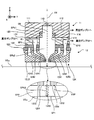
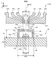
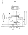
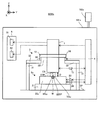
- FIG. 1 is a cross-sectional view showing the structure of the scanning electron microscope of the first embodiment.
- FIG. 2 is a cross-sectional view showing the structure of a beam irradiation device included in the scanning electron microscope of the first embodiment.
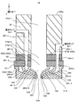
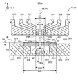
- FIG. 3 is a cross-sectional view showing the structure of the differential exhaust system of the first embodiment.
- FIG. 4 is a perspective view showing the structure of the differential exhaust system of the first embodiment in a state where a plurality of vacuum forming members are separated along the Z-axis direction.
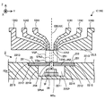
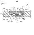
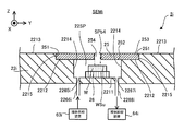
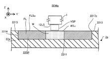
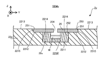
- FIG. 5 is a cross-sectional view showing the structure of the stage of the first embodiment.
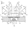
- FIG. 6 is a cross-sectional view showing an example of a position where a vacuum region is formed.
- FIG. 7 is a cross-sectional view showing an example of a position where a vacuum region is formed.
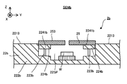
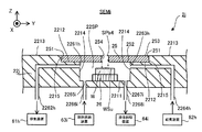
- FIG. 8 is a cross-sectional view showing the structure of the stage of the first embodiment.
- FIG. 9 is a cross-sectional view showing the structure of the stage of the second embodiment.
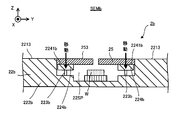
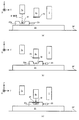
- FIG. 10 is a cross-sectional view showing an example of the movement of the lift pin in the stage of the second embodiment.
- FIG. 11 is a cross-sectional view showing an example of the movement of the lift pin in the stage of the second embodiment.
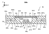
- FIG. 12 is a cross-sectional view showing the structure of the stage of the third embodiment.
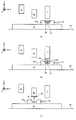
- FIG. 13 is a cross-sectional view showing an example of the movement of the lift pin in the stage of the third embodiment.
- FIG. 14 is a cross-sectional view showing an example of the movement of the lift pin in the stage of the third embodiment.
- FIG. 15 is a cross-sectional view showing the structure of the stage of the fourth embodiment.
- FIG. 16 is a cross-sectional view showing the structure of the stage of the fifth embodiment.
- FIG. 17 is a cross-sectional view showing the structure of the stage of the sixth embodiment.
- FIG. 18 is a cross-sectional view showing the structure of the stage of the seventh embodiment.
- FIG. 19 is a cross-sectional view showing the structure of the stage of the eighth embodiment.
- FIG. 20 is a cross-sectional view showing the structure of the stage of the ninth embodiment.
- FIG. 21 is a cross-sectional view showing the structure of the stage of the tenth embodiment.
- FIG. 22 is a cross-sectional view showing the structure of the stage device of the eleventh embodiment.
- FIG. 23 is a cross-sectional view showing the structure of the stage device of the twelfth embodiment.
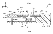
- FIG. 24 is a cross-sectional view showing the structure of the stage of the thirteenth embodiment.
- FIGS. 25 (a) to 25 (e) is a cross-sectional view showing an example of a flow of loading and unloading a sample through an opening.
- FIG. 26 is a cross-sectional view showing the structure of the stage device of the 14th embodiment.
- FIG. 27 is a cross-sectional view showing the structure of the stage device of the fifteenth embodiment.
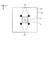
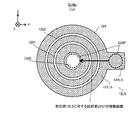
- FIG. 28 is a plan view showing an index mark formed on the stage device of the fifteenth embodiment.
- FIG. 29 is a cross-sectional view showing the structure of the stage device of the 16th embodiment.
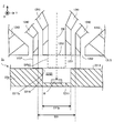
- FIG. 30 is a cross-sectional view showing the structure of the stage device of the 16th embodiment.
- FIG. 31 is a cross-sectional view showing the structure of the stage device of the 16th embodiment.
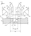
- FIG. 32 is a cross-sectional view showing the structure of the stage device of the 16th embodiment.
- FIG. 33 is a cross-sectional view showing the structure of a stage device for irradiating a sample with an electron beam through a facing surface different from the upper surface of the cover member in the 17th embodiment.
- FIG. 30 is a cross-sectional view showing the structure of the stage device of the 16th embodiment.
- FIG. 31 is a cross-sectional view showing the structure of the stage device of the 16th embodiment.
- FIG. 32 is a cross-sectional view showing the structure of the stage device of the 16th embodiment.
- FIG. 33 is a cross-sectional view showing the structure of a stage
- FIG. 34 is a cross-sectional view showing the structure of a stage device for irradiating a sample with an electron beam through a facing surface different from the upper surface of the cover member in the 17th embodiment.
- FIG. 35 is a cross-sectional view showing the structure of a stage apparatus for irradiating a sample with an electron beam through a facing surface different from the upper surface of the cover member in the 17th embodiment.
- FIG. 36 is a cross-sectional view showing the structure of the stage device of the 18th embodiment.
- FIG. 37 is a cross-sectional view showing another example of the structure of the stage apparatus of the 18th embodiment.
- FIG. 38 is a cross-sectional view showing another example of the structure of the scanning electron microscope of the eighteenth embodiment.
- FIG. 39 is a cross-sectional view showing the structure of the scanning electron microscope of the 19th embodiment.
- FIGS. 40 (a) to 40 (c) is a cross-sectional view showing a flow of operation of the scanning electron microscope of the 19th embodiment.
- FIGS. 41 (a) to 41 (c) is a cross-sectional view showing a flow of operation of the scanning electron microscope of the 19th embodiment.
- FIGS. 42 (a) to 42 (c) is a cross-sectional view showing a flow of operation of the scanning electron microscope of the 19th embodiment.
- FIG. 43 is a cross-sectional view showing a measuring device for measuring the state of the sample via the cover member.
- FIG. 44 is a cross-sectional view showing the structure of the scanning electron microscope of the 20th embodiment.
- FIGS. 45 (a) to 45 (c) is a cross-sectional view showing a flow of operation (particularly, a flow of movement of the shutter member 16t) of the scanning electron microscope of the twentieth embodiment.
- FIGS. 46 (a) to 46 (c) is a cross-sectional view showing a flow of operation (particularly, a flow of movement of the shutter member 16t) of the scanning electron microscope of the twentieth embodiment.
- FIG. 47 is a plan view showing the shape of the beam ejection surface 12LS of the 21st embodiment.
- FIG. 48 is a cross-sectional view showing the structure of the stage apparatus of the 22nd embodiment.
- FIG. 49 is a perspective view showing the holder of the 22nd embodiment.
- FIG. 50 is a cross-sectional view showing the structure of the stage device of the 23rd embodiment.
- FIG. 51 is a cross-sectional view showing the structure of the scanning electron microscope of the 24th embodiment.
- Sample W is, for example, a semiconductor substrate.
- the sample W may be an object different from the semiconductor substrate.
- the sample W may be, for example, a disk-shaped substrate having a diameter of about 300 mm and a thickness of about 750 micrometers to 800 micrometers.
- the sample W may be a substrate (or an object) having an arbitrary size and an arbitrary shape.
- the sample W may be a square substrate for a display such as a liquid crystal display element or a square substrate for a photomask.
- each of the X-axis direction and the Y-axis direction is a horizontal direction (that is, a predetermined direction in the horizontal plane), and the Z-axis direction is a vertical direction (that is, a direction orthogonal to the horizontal plane). Yes, in effect, in the vertical direction).
- the + Z side corresponds to the upper side (that is, the upper side) and the ⁇ Z side corresponds to the lower side (that is, the lower side).
- the ⁇ Z direction may be referred to as a gravity direction.
- the Z-axis direction is also a direction parallel to the optical axis AX of the beam optical system 11 described later included in the scanning electron microscope SEM.
- the rotation directions (in other words, the inclination direction) around the X-axis, the Y-axis, and the Z-axis are referred to as the ⁇ X direction, the ⁇ Y direction, and the ⁇ Z direction, respectively.
- FIG. 1 is a cross-sectional view showing the overall structure of the scanning electron microscope SEMa of the first embodiment.
- FIG. 1 does not show a cross section of some components of the scanning electron microscope SEMa.
- the scanning electron microscope SEMa includes a beam irradiation device 1, a stage device 2a, a support frame 3, a control device 4, and a pump system 5.
- the pump system 5 includes a vacuum pump 51 and a vacuum pump 52.
- the scanning electron microscope SEMa may include at least a chamber for accommodating the beam irradiation device 1, the stage device 2, and the support frame 3. Further, the scanning electron microscope SEMa may be provided with an air conditioner connected to this chamber to control at least one of the temperature and humidity of the space in the chamber (particularly, the space around the sample W). At least part of the space in the chamber may be atmospheric pressure space.
- the beam irradiating device 1 can emit an electron beam EB downward from the beam irradiating device 1.
- the beam irradiating device 1 can irradiate the sample W supported by the stage device 2a arranged below the beam irradiating device 1 with the electron beam EB.
- the beam irradiation device 1 forms a vacuum region VSP between the beam irradiation device 1 and the surface Vsu separated from the beam irradiation device 1 along the Z-axis direction, and then samples through the vacuum region VSP. Irradiate W with an electron beam EB.
- this surface VSu includes a surface that can face the beam irradiation device 1, it is referred to as “opposing surface VSu”.
- the facing surface VSu is a surface that intersects the Z axis. Since the detailed structure of the beam irradiation device 1 will be described later with reference to FIGS. 2 and 3, the description thereof will be omitted here. Further, the facing surface VSu will be described in detail later, and thus the description thereof will be omitted here.
- the stage device 2a is arranged below the beam irradiation device 1 (that is, on the ⁇ Z side).
- the stage device 2a includes a surface plate 21 and a stage 22a.
- the surface plate 21 is arranged on a support surface SF such as a floor.
- the stage 22a is arranged on the surface plate 21.
- a vibration isolator (not shown) is installed between the stage 22a and the surface plate 21 to prevent the vibration of the surface plate 21 from being transmitted to the stage 22a.
- Sample W is placed on the stage 22a. That is, the stage 22a can support the sample W.
- the stage 22a may be able to hold the sample W placed on the stage 22a.
- the stage 22a may hold the sample W by vacuum-adsorbing or electrostatically adsorbing the sample W.
- the stage 22a can release the retained sample W. Since the detailed structure of the stage 22a will be described later with reference to FIG. 5, the description thereof will be omitted here.
- the stage 22a can move along at least one of the X-axis direction, the Y-axis direction, the Z-axis direction, the ⁇ X direction, the ⁇ Y direction, and the ⁇ Z direction while supporting the sample W under the control of the control device 4. ..
- the stage device 2a includes a stage drive system 23.
- the stage drive system 23 moves the stage 22a by using, for example, an arbitrary motor (for example, a linear motor or the like).
- the stage device 2a includes a position measuring device 24 for measuring the position of the stage 22a.
- the position measuring device 24 includes, for example, at least one of an encoder and a laser interferometer.
- the control device 4 can specify the position of the sample W from the position of the stage 22a.
- the stage 22a may have a reference plate provided with a reference mark for associating the position of the electron beam EB by the beam irradiation device 1 with the position of the stage 22a (position in the XYZ direction).
- the stage drive system 23 may function as a position change device capable of changing the relative position between the stage 22a and / or the sample W and the beam irradiation device 1.
- the relative position of the sample W and the beam irradiator 1 in the direction along the XY plane changes. Therefore, when the stage 22a moves along the XY plane, the sample W in the direction along the XY plane and the irradiation region of the electron beam EB on the surface of the sample W (specifically, the surface facing the + Z side) WSu.
- the relative position of is changed. That is, when the stage 22a moves along the XY plane, the irradiation region of the electron beam EB moves with respect to the surface WSu of the sample W in the direction along the XY plane (that is, the direction along the surface WSu of the sample W). To do.
- the vacuum region VSP moves with respect to the facing surface VSu in the direction along the XY plane. Therefore, even if the stage 22 moves, the passage of the electron beam EB between the electron beam irradiation device 1 and the sample W (that is, the path through which the electron beam EB propagates) is included in at least a part of the vacuum region VSP. Is done. That is, the scanning electron microscope SEMa can irradiate the sample W with the electron beam EB via the vacuum region VSP even if the stage 22 moves.
- the control device 4 controls the stage drive system 23 to move the stage 22a along the Z axis so that the focus position of the electron beam EB is set on the surface WSu of the sample W (or in the vicinity of the surface WSu). You may let me.
- the focus position of the electron beam EB is such that the focus position corresponding to the image formation position of the beam optical system 11 (see FIG. 2) described later included in the electron beam irradiation device 1 or the blurring of the electron beam EB is minimized. It may be a position in the Z-axis direction.
- the stage drive system 23 may move the stage 22a under the control of the control device 4 so that the interval D becomes a desired interval D_target in cooperation with the interval adjusting system 34 described later.
- the control device 4 specifies the actual interval D based on the measurement result of the position measurement device 24 (furthermore, the measurement result of the position measurement device 15 that measures the position of the beam irradiation device 1 described later). At least one of the stage drive system 23 and the interval adjustment system 34 is controlled so that the specified interval D becomes the desired interval D_taget. Therefore, the position measuring devices 15 and 24 can also function as detection devices for detecting the interval D.
- the support frame 3 supports the beam irradiation device 1.
- the support frame 3 includes support legs 31 and support members 32.
- the support legs 31 are arranged on the support surface SF.
- a vibration isolator (not shown) may be installed between the support leg 31 and the support surface SF to prevent or reduce the transmission of the vibration of the support surface SF to the support leg 31.
- the support leg 31 is, for example, a member extending upward from the support surface SF.
- the support legs 31 support the support member 32.
- the support member 32 is an annular plate member having an opening 321 formed in the center in a plan view.
- the lower surface of the flange member 13 that supports the beam irradiation device 1 and extends outward from the outer surface of the beam irradiation device 1 is connected to the upper surface of the support member 32 via an interval adjusting system 34.
- the beam irradiation device 1 is arranged so as to penetrate the opening 321.
- the support frame 3 can support the beam irradiation device 1 so as to be lifted by the upper surface of the support member 32.
- the support frame 3 may function as a stopper for preventing the beam irradiation device 1 from moving toward the facing surface VSu so as to prevent the beam irradiation device 1 from colliding with the facing surface VSu.
- the support frame 3 may support the beam irradiation device 1 by a support method different from the support method shown in FIG. 1 as long as the beam irradiation device 1 can be supported.
- the support frame 3 instead of supporting the support frame 3 by the support legs 31, the support frame 3 may be supported by a suspension support mechanism.
- the anti-vibration pad is fixed to the top plate (ceiling wall) of the chamber accommodating the support frame 3, one end is connected to the lower end of the anti-vibration pad, and the other end of the wire made of steel is connected to the support frame 3. You may.
- the anti-vibration pad may include, for example, an air damper and / or a coil spring.
- An anti-vibration device (not shown) may be installed between the support legs 31 and the support member 32 to prevent or reduce the transmission of the vibration of the support surface SF to the support member 32.
- the interval adjustment system 34 adjusts the interval D between the beam irradiation device 1 and the facing surface VSu by moving the beam irradiation device 1 at least along the Z axis.
- the interval adjusting system 34 may move the beam irradiation device 1 along the Z-axis direction so that the interval D becomes a desired interval D_taget.
- a drive system that moves the beam irradiation device 1 by using the driving force of the motor a drive system that moves the beam irradiation device 1 by using the force generated by the piezoelectric effect of the piezo element, and the like.
- a drive system that moves the beam irradiation device 1 using a Coulomb force (for example, an electrostatic force generated between at least two electrodes) and a Lorentz force (for example, an electromagnetic force generated between a coil and a magnetic pole) are used. At least one of the drive systems for moving the beam irradiation device 1 may be used. However, if the distance D between the beam irradiation device 1 and the facing surface VSu can be kept fixed, a distance adjusting member such as a shim is used instead of the space adjusting system 34 with the support member 32 and the flange member 13. It may be arranged between.
- a distance adjusting member such as a shim is used instead of the space adjusting system 34 with the support member 32 and the flange member 13. It may be arranged between.
- the interval adjusting system 34 may move the beam irradiation device 1 along at least one of the X-axis direction, the Y-axis direction, the ⁇ X direction, the ⁇ Y direction, and the ⁇ Z direction.
- the interval adjusting system 34 may be referred to as a position changing device.
- the scanning electron microscope SEMa includes a position measuring device 15.
- the position measuring device 15 includes, for example, at least one of an encoder and a laser interferometer.
- the position measuring device 15 may measure the position of the beam irradiation device 1 in the XY direction, the posture in the ⁇ X direction, and the posture in the ⁇ Y direction.
- a measuring device for measuring the position of the beam irradiation device 1 in the XY direction, the posture in the ⁇ X direction, and the posture in the ⁇ Y direction may be provided separately from the position measuring device 15.
- the control device 4 controls the operation of the scanning electron microscope SEMa.
- the control device 4 may include, for example, an arithmetic unit and a memory.
- the arithmetic unit may include at least one of a CPU (Central Processing Unit), a GPU (Graphics Processing Unit), a DSP (Digital Signal Processor), and an MCU (Micro Control Unit).
- the control device 4 functions as a device that controls the operation of the scanning electron microscope SEMa by executing a computer program by the arithmetic unit.
- This computer program is a computer program for causing the control device 4 (for example, an arithmetic unit) to perform (that is, execute) an operation described later to be performed by the control device 4.
- this computer program is a computer program for making the control device 4 function so that the scanning electron microscope SEMa performs the operation described later.
- the computer program executed by the arithmetic unit may be recorded in a memory (that is, a recording medium) included in the control device 4, or may be an arbitrary storage medium built in the control device 4 or externally attached to the control device 4. It may be recorded in (for example, a hard disk or a semiconductor memory). Alternatively, the arithmetic unit may download the computer program to be executed from an external device of the control device 4 via the network interface.
- the control device 4 controls the beam irradiation device 1 so as to irradiate the sample W with the electron beam EB.
- the control device 4 controls at least one of the beam irradiation device 1 and the stage drive system 23 so that the electron beam EB is irradiated to a desired position in the XY plane of the surface WSu of the sample W.
- the control device 4 controls at least one of the stage drive system 23 and the interval adjustment system 34 so that the interval D between the beam irradiation device 1 and the facing surface VSu is a desired interval D_taget.
- the control device 4 may not be provided inside the scanning electron microscope SEMa, and may be provided as a server or the like outside the scanning electron microscope SEMa, for example.
- the control device 4 and the scanning electron microscope SEMa may be connected by a wired and / or wireless network (or a data bus and / or a communication line).
- a wired network for example, a network using a serial bus type interface represented by at least one of IEEE1394, RS-232x, RS-422, RS-423, RS-485 and USB may be used.
- a network using a parallel bus interface may be used.
- a network using an Ethernet (registered trademark) compliant interface represented by at least one of 10BASE-T, 100BASE-TX and 1000BASE-T may be used.
- a network using radio waves may be used.
- An example of a network using radio waves is a network conforming to IEEE802.1x (for example, at least one of wireless LAN and Bluetooth®).
- a network using infrared rays may be used.
- a network using optical communication may be used.
- the control device 4 and the scanning electron microscope SEMa may be configured so that various types of information can be transmitted and received via the network. Further, the control device 4 may be able to transmit information such as commands and control parameters to the scanning electron microscope SEMa via the network.
- the scanning electron microscope SEMa may include a receiving device that receives information such as commands and control parameters from the control device 4 via the network.
- the recording medium for recording the computer program executed by the arithmetic unit includes CD-ROM, CD-R, CD-RW, flexible disk, MO, DVD-ROM, DVD-RAM, DVD-R, DVD + R, and DVD-. At least one of optical disks such as RW, DVD + RW and Blu-ray (registered trademark), magnetic media such as magnetic tape, magneto-optical disks, semiconductor memory such as USB memory, and any other medium capable of storing a program is used. You may.
- the recording medium may include a device capable of recording a computer program (for example, a general-purpose device or a dedicated device in which the computer program is implemented in at least one form such as software and firmware).
- each process or function included in the computer program may be realized by a logical processing block realized in the control device 4 by the control device 4 (that is, a computer) executing the computer program. It may be realized by hardware such as a predetermined gate array (FPGA, ASIC) included in the control device 4, or a logical processing block and a partial hardware module that realizes a part of the hardware are mixed. It may be realized in the form of.
- a logical processing block realized in the control device 4 by the control device 4 (that is, a computer) executing the computer program. It may be realized by hardware such as a predetermined gate array (FPGA, ASIC) included in the control device 4, or a logical processing block and a partial hardware module that realizes a part of the hardware are mixed. It may be realized in the form of.
- FPGA predetermined gate array
- the scanning electron microscope SEMa irradiates the sample W with the electron beam EB so as to scan the surface WSu of the sample W with the electron beam EB, for example.
- the scanning electron microscope SEMa controls the stage drive system 23 to move the stage 22a along the XY plane so that the vacuum region VSP is formed on the first surface of the facing surface VSu. ..
- the beam irradiation device 1 moves the first surface of the surface WSu of the sample W via the vacuum region VSP. Is irradiated with an electron beam EB.
- the beam irradiation device 1 scans the first surface of the surface WSu of the sample W with the electron beam EB by deflecting the electron beam EB using a deflector (not shown) included in the beam irradiation device 1. .. While the beam irradiation device 1 is irradiating the first surface of the surface WSu of the sample W with the electron beam EB, the stage drive system 23 does not have to move the stage 22a along the XY plane. After the scanning of the first surface of the surface WSu of the sample W with the electron beam EB is completed, the scanning electron microscope SEMa has a vacuum region VSP on the second surface different from the first surface of the facing surface VSu.
- the stage drive system 23 is controlled to move the stage 22a along the XY plane so as to be formed.
- the beam irradiation device 1 moves the first surface of the surface WSu of the sample W via the vacuum region VSP.
- the second surface different from the above is irradiated with the electron beam EB.
- the beam irradiation device 1 scans the second surface of the surface WSu of the sample W with the electron beam EB by deflecting the electron beam EB using a deflector (not shown) included in the beam irradiation device 1. ..
- the stage drive system 23 does not have to move the stage 22a along the XY plane also during the period when the beam irradiation device 1 irradiates the second surface of the surface WSu of the sample W with the electron beam EB. .. After that, the same process is repeated until the irradiation (that is, scanning) of the electron beam EB to the target region of the surface WSu of the sample W to be irradiated with the electron beam EB is completed.
- the electrons generated by the irradiation of the sample W with the electron beam EB are emitted from the sample W.
- the electrons generated by the irradiation of the sample W with the electron beam EB include at least one of the reflected electrons from the sample W and the scattered electrons from the sample W.
- the scattered electrons may include secondary electrons.
- the electrons generated by the irradiation of the sample W with the electron beam EB are detected by the electron detector 114 (see FIG. 2) described later included in the beam irradiation device 1.
- the control device 4 generates (that is, acquires) information about the sample W based on the detection result of the electron detector 114.
- the control device 4 may generate information regarding the image of the sample W (hereinafter, referred to as “image information”) based on the detection result of the electron detector 114.
- image information may include information about the image of the surface WSu of the sample W.
- the electron detector 114 detects the electrons generated when the electron beam EB is irradiated while the beam irradiation device 1 is scanning the surface WSu of the sample W with the electron beam EB.
- the electron detector 114 is, for example, the electrons generated when the electron beam EB is irradiated to the first position of the surface WSu of the sample W, the sample W.
- the control device 4 can generate information on the distribution of the detected amount of electrons based on the detection result of the electron detector 114. That is, the control device 4 has an image having characteristics according to the amount of detected electrons based on the detection result of the electron detector 114 (that is, information on the detection result of electrons) and the information on the irradiation position of the electron beam EB. Image information regarding (a so-called SEM image, and in the first embodiment, an image of the surface WSu of the sample W) can be generated.
- FIG. 2 is a cross-sectional view showing the structure of the beam irradiation device 1 of the first embodiment.
- the beam irradiation device 1 includes a beam optical system 11 and a differential exhaust system 12.
- the beam optical system 11 includes a housing 111.
- the housing 111 is a cylindrical member in which a beam passing space SPb1 extending along the optical axis AX of the beam optical system 11 (that is, extending along the Z axis) is secured inside.
- the beam passing space SPb1 is used as a space through which the electron beam EB passes.
- the housing 111 may be made of a high magnetic permeability material in order to prevent the magnetic field) from affecting the electron beam EB passing through the beam passing space SPb1. Examples of high magnetic permeability materials include at least one of permalloy and silicon steel. The relative magnetic permeability of these high magnetic permeability materials is 1000 or more.
- the beam passing space SPb1 becomes a vacuum space during the period when the electron beam EB is irradiated.
- the beam passage space SPb1 is connected to the beam passage space SPb1 via an exhaust passage (that is, a pipeline, the same applies hereinafter) 112 formed in the housing 111 so as to be connected to (that is, connected to) the beam passage space SPb1.
- the vacuum pump 51 is connected.
- the vacuum pump 51 exhausts the beam passing space SPb1 (that is, discharges gas) so that the beam passing space SPb1 becomes a vacuum space, and depressurizes the pressure below the atmospheric pressure. Therefore, the vacuum space in the first embodiment may mean a space whose pressure is lower than the atmospheric pressure.
- the vacuum space is a space in which gas molecules exist only to the extent that the electron beam EB does not interfere with the appropriate irradiation of the sample W (in other words, the degree of vacuum does not interfere with the appropriate irradiation of the electron beam EB with the sample W).
- Space may be meant.
- the beam passing space SPb1 is a space outside the housing 111 (more specifically, a differential exhaust system 12 described later) via a beam ejection port (that is, an opening) 119 formed on the lower surface of the housing 111. It is connected to the beam passage space SPb2).
- the beam passing space SPb1 may be a vacuum space during the period when the electron beam EB is not irradiated.
- the beam optical system 11 further includes an electron gun 113 and an electron detector 114.
- the electron gun 113 emits an electron beam EB toward the ⁇ Z side. Instead of the electron gun 113, a photoelectric conversion surface that emits electrons when irradiated with light may be used.
- the electron detector 114 is a semiconductor type electron detector (that is, a semiconductor detector) using a pn junction or pin junction semiconductor. As described above, the electron detector 114 detects the electrons generated by the irradiation of the sample W with the electron beam EB (that is, the electrons emitted from the sample W).
- the electronic detector 114 may be arranged in the differential exhaust system 12.
- the beam optical system 11 may include an electromagnetic lens for controlling the electron beam EB emitted by the electron gun 113.
- this electromagnetic lens the amount of rotation (that is, the position in the ⁇ Z direction) of an image formed by the electron beam EB on a predetermined optical surface (for example, a virtual surface intersecting the optical path of the electron beam EB) and the magnification of the image.
- a predetermined optical surface for example, a virtual surface intersecting the optical path of the electron beam EB
- any one of the focal positions corresponding to the imaging position may be controlled.
- an electrostatic lens that controls the electron beam EB using an electric field may be used.
- the beam optical system 11 deflects the electron beam EB to the irradiation position of the electron beam EB on the surface WSu of the sample W (in particular, in a direction along the surface WSu (for example, at least one of the X-axis and the Y-axis).
- a deflector capable of controlling the irradiation position) in the direction along the line) may be provided.
- the differential exhaust system 12 is a member extending downward from the beam optical system 11.
- the differential exhaust system 12 is arranged below the beam optical system 11 (that is, on the ⁇ Z side).
- the differential exhaust system 12 is connected (that is, connected) to the beam optical system 11 below the beam optical system 11.
- the differential exhaust system 12 may be connected to the beam optical system 11 so that the upper surface of the differential exhaust system 12 is connected to the lower surface of the beam optical system 11.
- the differential exhaust system 12 may be integrated with the beam optical system 11 or may be separable from the beam optical system 11.
- a beam passage space SPb2 is formed inside the differential exhaust system 12.
- the beam passage space SPb2 is connected to the beam passage space SPb1 of the beam optical system 11 via an opening 120 formed on the upper surface of the differential exhaust system 12 (the surface on the + Z side in the example shown in FIG. 2). ..
- the beam passing space SPb2 is exhausted (that is, depressurized) by the vacuum pump 51 together with the beam passing space SPb1. Therefore, the beam passing space SPb2 becomes a vacuum space during the period in which the electron beam EB is irradiated.
- the beam passing space SPb2 is used as a space through which the electron beam EB from the beam passing space SPb1 passes.
- the beam passing space SPb2 may be a vacuum space during the period when the electron beam EB is not irradiated.
- the differential exhaust system 12 further includes an injection surface 12LS capable of facing a part of the facing surface VSu.
- the distance D between the injection surface 12LS and the facing surface VSu is a desired distance D_stage (for example, 10 ⁇ m or less). And it is aligned with respect to the facing surface VSu by at least one of the stage drive system 23 and the interval adjustment system 34 so as to be 1 ⁇ m or more).
- the distance D may be referred to as the distance between the injection surface 12LS and the facing surface VSu in the Z-axis direction.
- interval adjusting system 34 may be referred to as an interval control device.
- a beam ejection port (that is, an opening) 1250 is formed on the ejection surface 12LS.
- the differential exhaust system 12 does not have to have an injection surface 12LS capable of facing the facing surface VSu.
- the beam passing space SPb2 is connected to the beam passing space SPb3 outside the differential exhaust system 12 via the beam injection port 1250. That is, the beam passing space SPb1 is connected to the beam passing space SPb3 via the beam passing space SPb2. However, the beam passage space SPb2 may not be secured. That is, the beam passing space SPb1 may be directly connected to the beam passing space SPb3 without passing through the beam passing space SPb2.
- the beam passing space SPb3 is a space (for example, a local space) on the facing surface VSu.
- the beam passing space SPb3 is a space that is in contact with (that is, faces) the facing surface VSu.
- the beam passing space SPb3 is a space through which the electron beam EB passes between the beam irradiation device 1 and the facing surface VSu (specifically, between the injection surface 12LS and the facing surface VSu).
- the beam passing space SPb3 is exhausted (that is, depressurized) by the vacuum pump 51 together with the beam passing spaces SPb1 and SPb2. That is, the vacuum pump 51 exhausts the beam passing space SPb3 in a state where the differential exhaust system 12 (particularly, the injection surface 12LS) faces a part of the facing surface VSu.
- the vacuum pump 51 exhausts the beam passing space SPb3 in a state where the beam passing space SPb2 (particularly, the end portion thereof, substantially the beam ejection port 1250) faces a part of the facing surface VSu.
- each of the beam passing spaces SP1 and SPb2 can also function as an exhaust passage (that is, a pipeline) connecting the beam passing space SPb3 and the vacuum pump 51 in order to exhaust the beam passing space SPb3.
- the beam passing space SPb3 becomes a vacuum space during the period in which the electron beam EB is irradiated. Therefore, the electron beam EB emitted from the electron gun 113 irradiates the sample W through at least a part of the beam passing spaces SPb1 to SPb3, which are vacuum spaces.
- the beam passing space SPb3 may be a vacuum space during the period when the electron beam EB is not irradiated.
- the beam passing space SPb3 is located at a position farther from the vacuum pump 51 than the beam passing spaces SPb1 and SPb2.
- the beam passing space SPb2 is located at a position farther from the vacuum pump 51 than the beam passing space SPb1. Therefore, the degree of vacuum of the beam passing space SPb3 may be lower than the degree of vacuum of the beam passing spaces SPb1 and SPb2, and the degree of vacuum of the beam passing space SPb2 is higher than the degree of vacuum of the beam passing space SPb1. It can be low.
- the state of "the degree of vacuum in space B is lower than the degree of vacuum in space A" in the present embodiment means "the pressure in space B is higher than the pressure in space A".
- the vacuum pump 51 can set the vacuum degree of the beam passing space SPb3, which may have the lowest vacuum degree, to a vacuum degree that does not interfere with the appropriate irradiation of the electron beam EB to the sample W. Has exhaust capacity.
- the vacuum pump 51 maintains the pressure (ie, air pressure) of the beam passage space SPb3 below 1 ⁇ 10 -3 pascals (eg, approximately on the order of 1 ⁇ 10 -3 pascals to 1 ⁇ 10 -4 pascals). It may have an exhaust capacity that can be maintained).
- Such a vacuum pump 51 is used, for example, as a turbo molecular pump used as a main pump (or another type of high vacuum pump including at least one of a diffusion pump, a cryo pump and a sputter ion pump) and an auxiliary pump.
- a vacuum pump combined with a dry pump (or another type of low vacuum pump) may be used.
- the exhaust speed of the vacuum pump 51 may be an exhaust speed [m 3 / s] that can maintain the pressure (that is, atmospheric pressure) of the beam passing space SPb3 at 1 ⁇ 10 -3 pascal or less. ..
- the beam passing space SPb3 is not a closed space surrounded by some member (specifically, the housing 111 and the differential exhaust system 12) like the beam passing spaces SPb1 and SPb2. That is, the beam passing space SPb3 is an open space that is not surrounded by any member. Therefore, even if the beam passing space SPb3 is depressurized by the vacuum pump 51, gas flows into the beam passing space SPb3 from the periphery of the beam passing space SPb3. As a result, the degree of vacuum in the beam passing space SPb3 may decrease. Therefore, the differential exhaust system 12 maintains the degree of vacuum in the beam passing space SPb3 by performing differential exhaust between the beam irradiation device 1 and the facing surface VSu.
- the differential exhaust system 12 is relatively high between the beam irradiation device 1 and the sample W as compared with the surroundings by performing the differential exhaust between the beam irradiation device 1 and the facing surface VSu.
- a vacuum region VSP in which the degree of vacuum is maintained (for example, a local vacuum region VSP) is formed.
- two annular exhaust ports 1251 and 1252 (or at least one exhaust port of any shape) surrounding the beam injection port 1250 are formed on the injection surface 12LS of the differential exhaust system 12.
- the exhaust ports 1251 and 1252 can also be said to be exhaust grooves (in other words, recesses, the same applies hereinafter).
- a vacuum pump 52 is connected to the exhaust port 1251 via an exhaust passage (that is, a pipeline, the same applies hereinafter) EP1 formed in the differential exhaust system 12. That is, the first end (that is, one end) of the exhaust passage EP1 is connected to the vacuum pump 52 and is the second end (that is, the other end) of the exhaust passage EP1, which is substantially the exhaust port.
- the portion forming 1251) is in contact with the space between the injection surface 12LS and the facing surface VSu.
- a vacuum pump 52 is connected to the exhaust port 1252 via an exhaust passage (that is, a pipeline, the same applies hereinafter) EP2 formed in the differential exhaust system 12. That is, the first end (that is, one end) of the exhaust passage EP2 is connected to the vacuum pump 52 and is the second end (that is, the other end) of the exhaust passage EP2, which is substantially the exhaust port.
- the portion forming 1252) is in contact with the space between the injection surface 12LS and the facing surface VSu.
- the differential exhaust system 12 is provided via a first-stage exhaust path composed of the exhaust passage EP1 and the exhaust port 1251 and a second-stage exhaust path composed of the exhaust passage EP2 and the exhaust port 1252.
- Differential exhaust can be performed between the beam irradiation device 1 and the facing surface VSu. That is, in the example shown in FIG. 2, the differential exhaust system 12 is a differential exhaust system in which the number of exhaust stages is set to two.
- the number of exhaust stages of the differential exhaust system 12 is not limited to two, and when the number of exhaust stages is not two, the number of exhaust ports formed on the injection surface 12LS and the number of exhaust ports connected to the exhaust port are connected.
- the number of exhaust passages is appropriately set according to the number of exhaust stages.
- the vacuum pump 52 exhausts the beam passage space SPb3 through the exhaust passages EP1 and EP2 in a state where the differential exhaust system 12 (particularly, the injection surface 12LS) faces a part of the facing surface VSu. ..
- the vacuum pump 52 exhausts the beam passage space SPb3 in a state where the exhaust passages EP1 and EP2 (particularly, their ends, substantially the exhaust ports 1251 and 1252) face a part of the facing surface VSu.
- the differential exhaust system 12 can form a vacuum region VSP including the beam passing space SPb3 between the beam irradiation device 1 and the facing surface VSu.
- the differential exhaust in the present embodiment is performed between the facing surface VSu and the beam irradiation device 1 between one space (for example, the beam passing space SPb3) and another space different from one space. It corresponds to exhausting the beam passing space SPb3 while utilizing the property that the pressure difference is maintained by the exhaust resistance of the gap between the facing surface VSu and the beam irradiation device 1. Since the beam passage space SPb3 covers at least a part of the facing surface VSu, the vacuum region VSP also locally covers at least a part of the facing surface VSu. That is, the vacuum region VSP is in contact with (that is, faces) at least a part of the facing surface VSu.
- the vacuum pump 52 mainly exhausts at least a part of the space around the beam passing space SPb3 (particularly, the space located around the space where the vacuum region VSP is formed and having a higher pressure than the vacuum region VSP). It is used to relatively increase the degree of vacuum of the beam passage space SPb3. Therefore, the vacuum pump 52 may have an exhaust capacity capable of maintaining a vacuum degree lower than the vacuum degree maintained by the vacuum pump 51. That is, the exhaust capacity of the vacuum pump 52 may be lower than the exhaust capacity of the vacuum pump 51.
- the vacuum pump 52 may be a vacuum pump that includes a dry pump (or another type of low vacuum pump) but not a turbo molecular pump (or another type of high vacuum pump). Good.
- the exhaust speed of the vacuum pump 52 may be an exhaust speed [m 3 / s] that can maintain a vacuum degree lower than the vacuum degree maintained by the vacuum pump 51.
- the region that exhausts through a certain exhaust path among the multiple stages of exhaust paths is close to the beam passage space SPb3 (in other words,).
- the length of the exhaust path affects the degree of vacuum of the exhaust path. Therefore, the length of the first-stage exhaust path may be different from the length of the second-stage exhaust path.
- the shorter the exhaust path the more likely it is that the degree of vacuum in the exhaust path will increase. This is because the shorter the exhaust path, the smaller the space in which the gas molecules exist (that is, the space to be exhausted). Therefore, the exhaust path of the first stage may be shorter than the exhaust path of the second stage.
- the volume of the exhaust path affects the degree of vacuum of the exhaust path. Therefore, the volume of the first-stage exhaust path may be different from the volume of the second-stage exhaust path.
- the smaller the volume of the exhaust path the higher the possibility that the degree of vacuum of the exhaust path increases. This is because the smaller the volume of the exhaust path, the smaller the space in which the gas molecules exist (that is, the space to be exhausted). Therefore, the volume of the first-stage exhaust path may be smaller than the volume of the second-stage exhaust path.
- the area of the inner surface of the exhaust path affects the degree of vacuum of the exhaust path. Therefore, the area of the inner surface of the first-stage exhaust path may be different from the area of the inner surface of the second-stage exhaust path.
- the smaller the area of the inner surface of the exhaust path the higher the possibility that the degree of vacuum of the exhaust path increases. This is because the shorter the area of the inner surface of the exhaust path, the smaller the inner surface where the gas molecules are present in the exhaust path (that is, the region where the gas molecules should be recovered by the exhaust gas). Therefore, the area of the inner surface of the first-stage exhaust path may be smaller than the area of the inner surface of the second-stage exhaust path.
- the vacuum region VSP including the beam passage space SPb3 is formed in this way, at least a part of the facing surface VSu that does not face the beam passage space SPb3 (particularly, a portion away from the beam passage space SPb3). May be covered by a non-vacuum region having a lower degree of vacuum than the vacuum region VSP.
- the differential exhaust system 12 forms a vacuum region VSP in the space SP1 (see the enlarged view at the bottom of FIG. 2) including the beam passing space SPb3.
- the space SP1 includes, for example, a space in contact with at least one of the beam injection port 1250 and the exhaust ports 1251 and 1252.
- the space SP1 includes a space facing a portion of the facing surface VSu located directly below at least one of the beam injection port 1250 and the exhaust ports 1251 and 1252.
- the vacuum region VSP is not formed in the space SP2 around the space SP1 (that is, the space SP2 connected to the space SP2 around the space SP1 and see the enlarged view at the bottom of FIG. 2). That is, the space SP2 is a space having a higher pressure than the space SP1.
- the space SP2 includes, for example, a space away from the beam outlet 1250 and the exhaust ports 1251 and 1252.
- the space SP2 includes a space that cannot be connected to the beam injection port 1250, the exhaust ports 1251 and 1252 (furthermore, the beam passage space SPb2, the exhaust passage EP1 and the exhaust passage EP2) without passing through the space SP1.
- the space SP2 includes a space that can be connected to the beam injection port 1250, the exhaust ports 1251 and 1252 (furthermore, the beam passage space SPb2, the exhaust passage EP1 and the exhaust passage EP2) via the space SP1. Since the pressure of the space SP2 is higher than the pressure of the space SP1, there is a possibility that gas flows from the space SP2 into the space SP1, but the gas flowing from the space SP2 into the space SP1 is the outermost exhaust.
- the state in which the vacuum region VSP is locally formed is the state in which the vacuum region VSP is locally formed on the facing surface VSu (that is, the vacuum region VSP is locally formed in the direction along the facing surface VSu). It may mean a state formed in).
- the vacuum region VSP is a region in which gas molecules are present only to such an extent that the electron beam EB irradiates the sample W appropriately.
- the vacuum region VSP is, for example, a region where the pressure is 1 ⁇ 10 -3 Pascal or less (for example, generally on the order of 1 ⁇ 10 -3 Pascal to 1 ⁇ 10 -4 Pascal). That is, the pressure of the space SP1 in which the vacuum region VSP is formed is 1 ⁇ 10 -3 Pascal or less (for example, approximately on the order of 1 ⁇ 10 -3 Pascal to 1 ⁇ 10 -4 Pascal).
- the space SP2 in which the vacuum region VSP is not formed may be, for example, a space in which a relatively large number of gas molecules are present so as to hinder the appropriate irradiation of the sample W of the electron beam EB.
- the pressure in the space SP2 may be, for example, a pressure of 1 ⁇ 10 ⁇ 2 pascal or more.
- the space SP2 may be an atmospheric pressure space. In this way, the spaces SP1 and SP2 may be distinguished from their pressure (that is, atmospheric pressure).
- the differential exhaust system 12 includes the vacuum forming member 121, the vacuum forming member 122, the vacuum forming member 123, and the vacuum forming. It includes a member 124. Further, the vacuum forming member 124 includes a vacuum forming member 1241, a vacuum forming member 1242, and a vacuum forming member 1243.
- the differential exhaust system 12 may have any structure as long as the vacuum region VSP can be formed.
- FIG. 3 is a cross-sectional view showing the structure of the differential exhaust system 12 of the first embodiment.
- FIG. 5 is a perspective view showing the structure of the differential exhaust system 12 of the first embodiment in a state where the vacuum forming member 121 and the vacuum forming member 124 are separated along the Z-axis direction.
- the vacuum forming member 121 is a tubular member extending downward from the beam optical system 11.
- the vacuum forming member 121 is arranged below the beam optical system 11 (that is, on the ⁇ Z side).
- the vacuum forming member 121 is connected to the beam optical system 11 below the beam optical system 11.
- the vacuum forming member 121 may be connected to the beam optical system 11 so that the upper surface 121Su of the vacuum forming member 121 is connected to the lower surface of the beam optical system 11.
- the vacuum forming member 121 may be integrated with the beam optical system 11 or may be separable from the beam optical system 11.
- a beam passing space SPb2-1 forming a part of the beam passing space SPb2 is formed inside the vacuum forming member 121.
- the beam passage space SPb2-1 penetrates the vacuum forming member 121.
- the beam passage space SPb2-1 penetrates the vacuum forming member 121 from the lower surface 121Sl of the vacuum forming member 121 toward the upper surface 121Su of the vacuum forming member 121.
- the beam passing space SPb2-1 is a beam of the beam optical system 11 via one end of the beam passing space SPb2-1 (in FIG. 4, the end on the + Z side and the opening formed in the upper surface 121Su). It is connected to the passage space SPb1 (see FIG. 2).
- the beam passing space SP2-1 further passes through the other end of the beam passing space SPb2-1 (in FIG. 3, the end on the ⁇ Z side and the opening formed in the lower surface 121Sl), and the vacuum forming member 121 It is connected to the external space (more specifically, the beam passing space SPb2-2 of the vacuum forming member 122 described later).
- the vacuum forming member 121 is further formed with an exhaust passage EP1-1 forming a part of the exhaust passage EP1 and an exhaust passage EP2-1 forming a part of the exhaust passage EP2.
- the exhaust passages EP1-1 to EP2-1 are passages (that is, spaces) separated from each other.
- the exhaust passages EP1-1 to EP2-1 are passages separated from the beam passage space SPb2-1.
- Each of the exhaust passages EP1-1 to EP2-1 penetrates the vacuum forming member 121 from the lower surface 121Sl of the vacuum forming member 121 toward the other surface (side surface in the example shown in FIG. 3) of the vacuum forming member 121. There is.
- each of the exhaust passages EP1-1 to EP2-1 may include a passage portion extending along the Z axis and a passage portion extending along the direction intersecting the Z axis.
- Each of the exhaust passages EP1-1 to EP2-1 has one end of each of the exhaust passages EP1-1 to EP2-1 (in the example shown in FIG. 3, an opening formed on the side surface of the vacuum forming member 121). It is connected to the vacuum pump 52 via.
- Each of the exhaust passages EP1-1 to EP2-1 further passes through the other end of each of the exhaust passages EP1-1 to EP2-1 (in the example shown in FIG. 5, an opening formed in the lower surface 121Sl). It is connected to the space outside the vacuum forming member 121 (more specifically, the exhaust passages EP1-2 to EP2-2 formed in the vacuum forming member 122 described later).
- the vacuum forming member 122 is a member extending downward from the vacuum forming member 121.
- the vacuum forming member 122 is arranged below the vacuum forming member 121 (that is, on the ⁇ Z side).
- the vacuum forming member 122 is connected to the vacuum forming member 121 below the vacuum forming member 121.
- the vacuum forming member 122 may be connected to the vacuum forming member 121 so that the upper surface 122Su of the vacuum forming member 122 is connected to the lower surface 121Sl of the vacuum forming member 121.
- the vacuum forming member 122 may be integrated with the vacuum forming member 121 or may be separable from the vacuum forming member 121.
- a beam passing space SPb2-2 forming a part of the beam passing space SPb2 is formed inside the vacuum forming member 122.
- the beam passage space SPb2-2 penetrates the vacuum forming member 122.
- the beam passage space SPb2-2 penetrates the vacuum forming member 122 from the lower surface 122Sl of the vacuum forming member 122 toward the upper surface 122Su of the vacuum forming member 122.
- the beam passing space SPb2-2 is a vacuum forming member via one end of the beam passing space SPb2-2 (in the example shown in FIG. 3, the end on the + Z side and the opening formed in the upper surface 122Su). It is connected to the beam passage space SPb2-1 of 121.
- the beam passage space SP2-2 is further evacuated through the other end of the beam passage space SPb2-2 (in the example shown in FIG. 3, the end on the ⁇ Z side, which is an opening formed in the lower surface 122Sl). It is connected to the space outside the forming member 122 (more specifically, the beam passing space SPb2-3 of the vacuum forming member 123 described later).
- the vacuum forming member 122 is further formed with an exhaust passage EP1-2 forming a part of the exhaust passage EP1.
- the exhaust passage EP1-2 is connected to the exhaust passage EP1-1 of the vacuum forming member 121 via one end of the exhaust passage EP1-2 (in the example shown in FIG. 3, an opening formed in the upper surface 122Su). ing.
- the exhaust passage EP1-2 is a space (more specifically) outside the vacuum forming member 122 via the other end of the exhaust passage EP1-2 (in the example shown in FIG. 3, an opening formed in the lower surface 122Sl). Is connected to the exhaust passage EP1-3) formed in the vacuum forming member 123 described later.
- the vacuum forming member 122 is further formed with an exhaust passage EP2-2 forming a part of the exhaust passage EP2.
- the exhaust passage EP2-2 is connected to the exhaust passage EP2-1 of the vacuum forming member 121 via one end of the exhaust passage EP2-2 (in the example shown in FIG. 3, an opening formed in the upper surface 122Su). ing.
- the exhaust passage EP2-2 is a space (more specifically) outside the vacuum forming member 122 via the other end of the exhaust passage EP2-2 (in the example shown in FIG. 3, an opening formed in the lower surface 122Sl). Is connected to the exhaust passage EP2-3) formed in the vacuum forming member 123 described later.
- the vacuum forming member 123 is a member extending downward from the vacuum forming member 122.
- the vacuum forming member 123 is arranged below the vacuum forming member 122 (that is, on the ⁇ Z side).
- the vacuum forming member 123 is connected to the vacuum forming member 122 below the vacuum forming member 122.
- the vacuum forming member 123 may be connected to the vacuum forming member 122 so that the upper surface 123Su of the vacuum forming member 123 is connected to the lower surface 122Sl of the vacuum forming member 122.
- the vacuum forming member 123 may be integrated with the vacuum forming member 122 or may be separable from the vacuum forming member 122.
- a beam passing space SPb2-3 forming a part of the beam passing space SPb2 is formed inside the vacuum forming member 123.
- the beam passage space SPb2-3 penetrates the vacuum forming member 123.
- the beam passage space SPb2-3 penetrates the vacuum forming member 123 from the lower surface 123Sl of the vacuum forming member 123 toward the upper surface 123Su of the vacuum forming member 123.
- the beam passing space SPb2-3 is a vacuum forming member via one end of the beam passing space SPb2-3 (in the example shown in FIG. 3, the end on the + Z side and the opening formed in the upper surface 123Su). It is connected to the beam passage space SPb2-2 of 122.
- the beam passage space SP2-3 is further evacuated through the other end of the beam passage space SPb2-3 (in the example shown in FIG. 3, the end on the ⁇ Z side, which is an opening formed in the lower surface 123Sl). It is connected to the space outside the forming member 123 (more specifically, the beam passing space SPb2-4 of the vacuum forming member 124 described later).
- the vacuum forming member 123 is further formed with an exhaust passage EP1-3 forming a part of the exhaust passage EP1.
- the exhaust passage EP1-3 is connected to the exhaust passage EP1-2 of the vacuum forming member 122 via one end of the exhaust passage EP1-3 (in the example shown in FIG. 3, an opening formed in the upper surface 123Su). ing.
- the exhaust passage EP1-3 is a space (more specifically) outside the vacuum forming member 123 via the other end of the exhaust passage EP1-3 (in the example shown in FIG. 3, an opening formed in the lower surface 123Sl). Is connected to the exhaust passage EP1-4) formed in the vacuum forming member 124 described later.
- the vacuum forming member 123 is further formed with an exhaust passage EP2-3 forming a part of the exhaust passage EP2.
- the exhaust passage EP2-3 is connected to the exhaust passage EP2-2 of the vacuum forming member 122 via one end of the exhaust passage EP2-3 (in the example shown in FIG. 3, an opening formed in the upper surface 123Su). ing.
- the exhaust passage EP2-3 is a space (more specifically) outside the vacuum forming member 123 via the other end of the exhaust passage EP2-3 (in the example shown in FIG. 3, an opening formed in the lower surface 123Sl). Is connected to the exhaust passage EP2-4) formed in the vacuum forming member 124 described later.
- the vacuum forming member 124 is a member extending downward from the vacuum forming member 123.
- the vacuum forming member 124 is arranged below the vacuum forming member 123 (that is, on the ⁇ Z side).
- the vacuum forming member 124 is connected to the vacuum forming member 123 below the vacuum forming member 123.
- the vacuum forming member 124 may be connected to the vacuum forming member 123 so that the upper surface 124Su of the vacuum forming member 124 is connected to the lower surface 123Sl of the vacuum forming member 123.
- the vacuum forming member 124 may be integrated with the vacuum forming member 123 or may be separable from the vacuum forming member 123.
- the vacuum forming member 124 includes the vacuum forming members 1241 to 1243.
- Each of the vacuum forming members 1241 to 1243 is arranged below the vacuum forming member 123 (that is, on the ⁇ Z side).
- Each of the vacuum forming members 1241 to 1243 is connected to the vacuum forming member 123 below the vacuum forming member 123.
- each of the vacuum forming members 1241 to 1243 may be connected to the vacuum forming member 123 so that the upper surface of each of the vacuum forming members 1241 to 1243 is connected to the lower surface 123Sl of the vacuum forming member 123.
- Each of the vacuum forming members 1241 to 1243 may be integrated with the vacuum forming member 123 or may be separable from the vacuum forming member 123.
- the vacuum forming member 124 has a structure in which the vacuum forming members 1241 to 1243 are laminated with a gap secured between them.
- the vacuum forming member 124 may have a structure in which the vacuum forming members 1241 to 1243 are laminated in a nested manner.
- the vacuum forming members 1241 to 1243 having the same shape are laminated. It also includes a structure in which at least two vacuum forming members 1241 to 1243 having different shapes are laminated.
- a beam passing space SPb2-4 forming a part of the beam passing space SPb2 is formed inside the vacuum forming member 1241.
- the beam passage space SPb2-4 penetrates the vacuum forming member 1241.
- the beam passage space SPb2-4 faces from the lower surface of the vacuum forming member 1241 (that is, at least a part of the injection surface 12LS) to the upper surface of the vacuum forming member 1241 (that is, a part of the upper surface 124Su). It penetrates the vacuum forming member 1241.
- the beam passing space SPb2-4 is via one end of the beam passing space SPb2-4 (in the example shown in FIG. 3, the end on the + Z side, which is an opening formed on the upper surface of the vacuum forming member 1241).
- the beam passing space SP2-4 is further the other end of the beam passing space SPb2-4 (in the example shown in FIG. 3, the end on the ⁇ Z side, and the beam ejection port formed on the lower surface of the vacuum forming member 1241. It is connected to the space outside the vacuum forming member 1241 (more specifically, the beam passing space SPb3) via 1250).
- the vacuum forming member 1242 and the vacuum forming member 1241 form an exhaust passage EP1-4 forming a part of the exhaust passage EP1.
- the inner surface of the vacuum forming member 1242 is the vacuum forming member 1241 in a state where a gap is secured between the inner surface of the vacuum forming member 1242 and the outer surface of the vacuum forming member 1241. It is aligned with the vacuum forming member 1241 so as to face the outer side surface.
- the gap between the inner surface of the vacuum forming member 1242 that is, the surface facing the optical axis AX side
- the outer surface of the vacuum forming member 1241 that is, the surface facing the opposite side of the optical axis AX.
- the exhaust passage EP1-4 is connected to the exhaust passage EP1-3 of the vacuum forming member 123 via one end of the exhaust passage EP1-4 (in the example shown in FIG. 3, an annular opening formed in the upper surface 124Su). You are connected.
- the exhaust passage EP1-4 is a space outside the vacuum forming member 124 via the other end of the exhaust passage EP1-4 (in the example shown in FIG. 3, the annular exhaust port 1251 formed on the injection surface 12LS). (More specifically, it is connected to the space between the differential exhaust system 12 and the facing surface VSu).
- the vacuum forming member 1243 and the vacuum forming member 1242 form an exhaust passage EP2-4 forming a part of the exhaust passage EP2.
- the inner surface of the vacuum forming member 1243 is the vacuum forming member 1242 in a state where a gap is secured between the inner surface of the vacuum forming member 1243 and the outer surface of the vacuum forming member 1242. It is aligned with respect to the vacuum forming member 1242 so as to face the outer side surface. As a result, the gap between the inner surface of the vacuum forming member 1243 and the outer surface of the vacuum forming member 1242 can be used as the exhaust passage EP2-4.
- the exhaust passage EP2-4 is connected to the exhaust passage EP2-3 of the vacuum forming member 123 via one end of the exhaust passage EP2-4 (in the example shown in FIG. 3, an annular opening formed in the upper surface 124Su). You are connected.
- the exhaust passage EP2-4 passes through the other end of the exhaust passage EP2-4 (in the example shown in FIG. 3, the exhaust port 1252 formed on the injection surface 12LS), and the space outside the vacuum forming member 124 (more than that). Specifically, it is connected to the space between the differential exhaust system 12 and the facing surface VSu).
- Each of the vacuum forming members 1241 to 1243 may have any shape as long as the beam passage space SPb2-4 and the exhaust passages EP1-4 to EP2-4 can be formed.
- the vacuum forming member 124 may have any shape as long as the beam passage space SPb2-4 and the exhaust passages EP1-4 to EP3-4 can be formed.
- the vacuum forming member 124 does not have to be separated into a plurality of vacuum forming members 1241 to 1243 as long as the beam passage space SPb2-4 and the exhaust passages EP1-4 to EP2-4 can be formed.
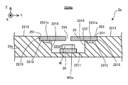
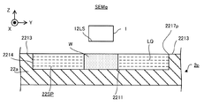
- FIG. 5 is a cross-sectional view showing the structure of the stage 22a of the first embodiment.
- the stage 22a includes an upper surface 2211, an upper surface 2212, an upper surface 2213, an inner side surface 2214, and an inner side surface 2215.
- Each of the upper surfaces 2211 to 2213 is a surface facing upward (that is, + Z side).
- Each of the upper surfaces 2211 to 2213 is a plane along the XY plane. However, at least one of the upper surfaces 2211 to 2213 may include a plane inclined with respect to the XY plane and / or a plane not flat.
- Each of the inner side surfaces 2214 to 2215 is a surface facing the inside (that is, the optical axis AX side) with respect to the optical axis AX.
- Each of the inner surfaces 2214 to 2215 is a surface along the Z axis. However, at least one of the inner side surfaces 2214 to 2215 may include a surface inclined with respect to the Z axis.
- the upper surface 2211 is located below the upper surface 2212 (further, the upper surface 2213).
- the upper surface 2212 (further, the upper surface 2213) is located above the upper surface 2211.
- the upper surface 2211 is located inside the upper surface 2212 (furthermore, the upper surface 2213).
- the upper surface 2212 (further, the upper surface 2213) is located outside the upper surface 2211.
- the upper surface 2212 is, for example, a surface whose shape in the plane along the XY plane is a frame shape having an opening inside (for example, an annular frame shape).
- the outer end of the upper surface 2211 and the inner end of the upper surface 2212 are connected via an inner side surface 2214.
- the inner side surface 2214 is a surface extending along the Z-axis direction from the outer end portion of the upper surface 2211 toward the inner end portion of the upper surface 2212. As a result, a space recessed from the upper surface 2213 to the ⁇ Z side is formed on the stage 22a.
- the stage 22 includes the stage 26 in the sample chamber 22SP.
- the stage 26 is arranged on the upper surface 2211 (or other position).
- the stage 26 is supported by an upper surface 2211 (or any other support member).
- Sample W is placed on the stage 26.
- the stage 26 can support the sample W.
- the stage 26 may be able to hold the sample W placed on the stage 26.
- the stage 26 may hold the sample W by vacuum-adsorbing or electrostatically adsorbing the sample W.
- the stage 26 can release the retained sample W. That is, the stage 22a can support the sample W via the stage 26.
- the stage 22a does not have to include the stage 26.
- the sample W may be placed on the upper surface 2211. That is, the sample W may be supported by the top surface 2211. Alternatively, the sample W may be supported by the inner surface 2214. Alternatively, the sample W may be supported by any other support member in the sample chamber 22SP.
- the stage 26 can move along at least one of the X-axis direction, the Y-axis direction, the Z-axis direction, the ⁇ X direction, the ⁇ Y direction, and the ⁇ Z direction while supporting the sample W under the control of the control device 4. You may. Therefore, the stage device 2a may include a stage drive system (not shown) for moving the stage 26. As the stage drive system, for example, an arbitrary motor (for example, a linear motor or the like) may be used to move the stage 26. The stage drive system may move the stage 26 in at least a part of the sample chamber 22SP. If the stage 26 does not move, the stage 26 may be referred to as a holder.
- a stage drive system for example, an arbitrary motor (for example, a linear motor or the like) may be used to move the stage 26.
- the stage drive system may move the stage 26 in at least a part of the sample chamber 22SP. If the stage 26 does not move, the stage 26 may be referred to as a holder.
- the upper surface 2212 is located below the upper surface 2213.
- the upper surface 2213 is located above the upper surface 2212.
- the upper surface 2212 is located inside the upper surface 2213.
- the upper surface 2213 is located outside the upper surface 2212.
- the upper surface 2213 is, for example, a surface whose shape in the plane along the XY plane is a frame shape having an opening on the inside. Since the upper surface 2213 is located outside the upper surface 2212, the upper surface 2213 may be referred to as an outer peripheral surface.
- the outer end of the upper surface 2212 and the inner end of the upper surface 2213 are connected via the inner side surface 2215.
- the inner side surface 2215 is a surface extending along the Z-axis direction from the outer end portion of the upper surface 2212 toward the inner end portion of the upper surface 2213.
- a step is formed on the stage 22a due to the upper surface 2212 and the upper surface 2213 being located at different positions in the Z-axis direction.
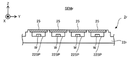
- a cover member 25 is arranged on the upper surface 2212.
- the cover member 25 has an upper surface 2212 such that the outer surface (that is, the surface facing the outside (that is, the side opposite to the optical axis AX) of the optical axis AX) 251 of the cover member 25 faces the inner side surface 2215. Is placed in. That is, the cover member 25 is arranged at the step formed by the upper surface 2212 and the upper surface 2213. In this case, the upper surface 2212 can function as a support surface that supports the cover member 25 from below.
- the outer surface 251 of the cover member 25 may or may not be in contact with the inner surface 2215.
- the inner side surface 2215 may function as a support surface for supporting the cover member 25.
- the cover member 25 is fitted in the step formed by the upper surface 2212 and the upper surface 2213.
- the cover member 25 is a plate-shaped member.
- the cover member 25 is a member that covers the upper part of the sample chamber 22SP in a state where the cover member 25 is arranged on the upper surface 2212. Therefore, when the cover member 25 is arranged on the upper surface 2212, there is a space between the upper surface 2211 of the stage 22a and the lower surface (that is, the surface facing downward ( ⁇ Z side)) 252 of the cover member 25. It becomes the sample chamber 22SP.
- the space surrounded by the upper surface 2211 and the inner side surface 2214 of the stage 22a and the lower surface 252 of the cover member 25 is the sample chamber 22SP. That is, the cover member 25 forms the sample chamber 22SP together with the stage 22a.
- the lower surface 252 of the cover member 25 includes a surface facing (that is, contacting) the sample chamber 22SP.
- the upper surface 253 of the cover member 25 is a plane along the XY plane.
- the height of the upper surface 253 of the cover member 25 is the same as the height of the upper surface 2213 of the stage 22a when the cover member 25 is arranged on the upper surface 2212. That is, in the state where the cover member 25 is arranged on the upper surface 2212, the position of the upper surface 253 of the cover member 25 in the Z-axis direction is the same as the position of the upper surface 2213 of the stage 22a in the Z-axis direction.
- the thickness of the cover member 25 (that is, the size in the Z-axis direction) is set to be the same as the height of the step formed by the upper surface 2212 and the upper surface 2213.
- the cover The height of the step formed by the upper surface 2212 and the upper surface 2213 is set to be the same as the thickness of the cover member 25.
- the thickness of the cover member 25 is set to be the same as the size of the inner side surface 2215 of the stage 22a in the Z-axis direction.
- the size of the inner side surface 2215 of the stage 22a in the Z-axis direction is set to be the same as the thickness of the cover member 25.
- the beam irradiation device 1 may form a vacuum region VSP between the beam irradiation device 1 and the cover member 25.
- the beam irradiation device 1 may form a vacuum region VSP between the injection surface 12LS of the beam irradiation device 1 and the upper surface 253 of the cover member 25.
- the beam irradiation device 1 may form a vacuum region VSP that is in contact with (that is, faces) at least a part of the upper surface 253 of the cover member 25.
- the facing surface VSu described above may include at least a part of the upper surface 253 of the cover member 25.
- a part of the upper surface 253 of the cover member 25 is in contact with the vacuum region VSP, while another part of the upper surface 253 of the cover member 25 is not in contact with the vacuum region VSP (for example, is in contact with the non-vacuum region).
- the vacuum region VSP may be formed.
- the beam irradiation device 1 may form the vacuum region VSP so that the entire upper surface 253 of the cover member 25 is in contact with the vacuum region VSP.
- the beam irradiation device 1 may form the vacuum region VSP between the beam irradiation device 1 and the stage 22a.
- the beam irradiation device 1 may form a vacuum region VSP between the injection surface 12LS of the beam irradiation device 1 and the upper surface 2213 of the stage 22a.
- the beam irradiation device 1 may form a vacuum region VSP in contact with at least a part of the upper surface 2213 of the stage 22a.
- the facing surface VSu described above may include at least a part of the upper surface 2213 of the stage 22a.
- the other part of the upper surface 2213 of the stage 22a is not in contact with the vacuum region VSP (for example, in the non-vacuum region).
- the vacuum region VSP may be formed so as to be in contact with each other.
- the beam irradiation device 1 may form the vacuum region VSP so that the entire upper surface 2213 of the stage 22a is in contact with the vacuum region VSP.
- the beam irradiation device 1 forms a vacuum region VSP between the injection surface 12LS of the beam irradiation device 1 and the upper surface 2211 and / or 2212 of the stage 22a. You may.
- the beam irradiator 1 may form a vacuum region VSP in contact with at least a portion of the upper surface 2211 and / or 2212 of the stage 22a.
- the facing surface VSu described above may include at least a part of the upper surface 2211 and / or 2212 of the stage 22a.
- the beam irradiation device 1 may form the vacuum region VSP straddling the upper surface 253 of the cover member 25 and the upper surface 2213 of the stage 22a. That is, the beam irradiation device 1 may form a vacuum region VSP that is in contact with at least a part of the upper surface 253 of the cover member 25 and at least a part of the upper surface 2213 of the stage 22a.
- the size of the cover member 25 in one direction along the XY plane may be larger than the size of the vacuum region VSP in one direction along the XY plane.
- the size of the cover member 25 in the X-axis direction may be larger than the size of the vacuum region VSP in the X-axis direction.
- the size of the cover member 25 in the Y-axis direction may be larger than the size of the vacuum region VSP in the Y-axis direction.
- FIG. 5 shows an example in which the size of the cover member 25 in the Y-axis direction is larger than the size of the vacuum region VSP in the Y-axis direction.
- a part of the upper surface 253 of the cover member 25 is in contact with the vacuum region VSP, while another part of the upper surface 253 of the cover member 25 is not in contact with the vacuum region VSP (for example, it is in contact with the non-vacuum region).
- the size of the vacuum region VSP in one direction along the XY plane depends on the size of the exhaust port 1252 located on the outermost side in one direction along the XY plane.
- the size of the exhaust port 1252 in one direction along the XY plane is the size of the exhaust port 1252 in one direction along the XY plane. It may mean the diameter.
- the size of the vacuum region VSP may be smaller than the size of the exhaust port 1252. This is because the exhaust port 1252 discharges the gas flowing into the space SP1 in which the vacuum region VSP is formed from the space SP2 in which the vacuum region VSP is not formed from the space SP1. Therefore, the exhaust port 1252 does not form the vacuum region VSP.
- the size of the cover member 25 in one direction along the XY plane may be larger than the size of the exhaust port 1252 in one direction along the XY plane.
- the size of the vacuum region VSP in one direction along the XY plane is smaller than the size of the cover member 25 in one direction along the XY plane.
- the size of the cover member 25 in one direction along the XY plane is larger than the size of the vacuum region VSP in one direction along the XY plane. May be small.
- the size of the cover member 25 in one direction along the XY plane may be smaller than the size of the exhaust port 1252 in one direction along the XY plane.
- the size of the cover member 25 in one direction along the XY plane may be the same as the size of the vacuum region VSP in one direction along the XY plane.
- the size of the cover member 25 in one direction along the XY plane may be the same as the size of the exhaust port 1252 in one direction along the XY plane.
- the beam irradiation device 1 typically forms a vacuum region VSP that straddles the upper surface 253 of the cover member 25 and the upper surface 2213 of the stage 22a.
- the cover member 25 In the state where the cover member 25 is arranged on the upper surface 2212, since the cover member 25 covers the upper part of the sample chamber 22SP, a cover member 25 different from the sample W is located between the sample W and the beam irradiation device 1. are doing. That is, the sample W (furthermore, the sample chamber 22SP) is located on the opposite side of the cover member 25 from the beam irradiation device 1. Therefore, the beam irradiation device 1 irradiates the sample W with the electron beam EB via the cover member 25. On the other hand, when the electron beam EB is irradiated on the cover member 25, the electric charge caused by the electron beam EB may be accumulated in the cover member 25.
- the cover member 25 is formed with a through hole 254 through which the electron beam EB can pass.
- the through hole 254 penetrates the cover member 25 from the upper surface 253 of the cover member 25 toward the lower surface 252 of the cover member 25.
- the stage drive system 23 moves the stage 22a so that the through hole 254 is arranged in the passage of the electron beam EB, and the beam irradiation device 1 moves the electron through the through hole 254 of the cover member 25.
- the beam EB is applied to the sample W.
- the beam irradiating device 1 irradiates the sample W with the electron beam EB without passing through the main body of the cover member 25 (that is, a portion where electric charges may be accumulated). As a result, the possibility of charge-up occurring is reduced.
- irradiating the sample W with the electron beam EB through the through hole 254 of the cover member 25 and irradiating the sample W with the electron beam EB through the main body of the cover member 25 are each performed through the cover member 25.
- the stage drive system 23 moves the stage 22a with respect to the beam irradiation device 1 (and thus the vacuum forming member 121) so that the through hole 254 is arranged in the passage of the electron beam EB.
- the beam irradiation device 1 (and thus the vacuum forming member 121) may be moved with respect to the stage 22a.
- the size of the through hole 254 in one direction along the XY plane is smaller than the size of the vacuum region VSP in one direction along the XY plane.
- the size of the through hole 254 in one direction along the XY plane may be larger than the size of the vacuum region VSP in one direction along the XY plane.
- the size of the through hole 254 in one direction along the XY plane may be the same as the size of the vacuum region VSP in one direction along the XY plane.
- the beam irradiation device 1 deflects the electron beam EB by using the deflector as described above, the size of the through hole 254 in one direction along the XY plane is such that the stage 22a moves.
- the size may be such that the electron beam EB deflected by the deflector can pass through under no circumstances.
- the size of the through hole 254 in one direction along the XY plane is such that the region through which the electron beam EB deflected by the deflector passes (particularly, the through hole 254 is formed) when the stage 22a is not moving. It may be larger than the size in one direction along the XY plane of the region through which the electron beam EB passes at the position where the electron beam EB passes.
- the beam irradiating device 1 deflects the electron beam EB, the beam irradiating device 1 does not go through the main body of the cover member 25 (that is, a portion where electric charges may be accumulated).
- the EB can be applied to the sample W.
- the smaller the through hole 254 the smaller the region of the surface WSu of the sample W that can be irradiated with the electron beam EB through the through hole 254. Become. That is, in a state where the position of the sample W in the sample chamber 22SP is fixed, the smaller the through hole 254, the more the cover member 25 other than the through hole 254 of the surface WSu of the sample W must pass through. The area where the electron beam EB cannot be irradiated becomes large.
- the stage 26 moves along the direction along the XY plane in the sample chamber 22SP. May be good.
- the stage 26 moves, the relative positions of the sample W supported by the stage 26 and the cover member 25 change. That is, the relative position between the sample W supported by the stage 26 and the through hole 254 of the cover member 25 changes.
- the stage 26 can function as a position changing device for changing the relative position between the sample W and the cover member 25 (particularly, the through hole 254).
- the region of the surface WSu of the sample W that can be irradiated with the electron beam EB through the through hole 254 becomes larger than that in the case where the stage 26 does not move. Therefore, the stage 26 may move in cooperation with the stage 22a so that the electron beam EB is irradiated to a desired position of the surface WSu of the sample W through the through hole 254.
- the beam irradiation device 1 is the upper end portion of the through hole 254 (specifically, the end portion on the beam irradiation device 1 side, and the through hole 254 is the cover member 25.
- a vacuum region VSP may be formed in contact with the opening) formed on the upper surface 253.
- the facing surface VSu described above may include at least a part of a virtual plane defining the upper end of the through hole 254.
- the sample chamber 22SP When the through hole 254 is formed, the sample chamber 22SP is connected to the beam passage space SPb3 (that is, the vacuum region VSP) through the through hole 254. Therefore, the sample chamber 22SP (furthermore, the space inside the through hole 254) is exhausted (that is, depressurized) by the vacuum pump 51 together with the beam passing space SPb3. Therefore, the sample chamber 22SP (furthermore, the space inside the through hole 254) becomes a vacuum space during the period in which the electron beam EB is irradiated, similarly to the beam passing space SPb3.
- the beam passing space SPb4 through which the electron beam EB passes in the sample chamber 22SP also becomes a vacuum space during the period in which the electron beam EB is irradiated. Therefore, the beam irradiating device 1 can irradiate the sample W with the electron beam EB via at least a part of the beam passing space SPb1 to SPb4, which is a vacuum space.
- the vacuum pump 51 exhausts the beam passage space SPb4, which may have the lowest degree of vacuum, so that the degree of vacuum does not interfere with the appropriate irradiation of the electron beam EB on the sample W. It may have the ability.
- the vacuum pump 51 maintains the pressure (ie, air pressure) of the beam passage space SPb4 below 1 ⁇ 10 -3 pascals (eg, approximately on the order of 1 ⁇ 10 -3 pascals to 1 ⁇ 10 -4 pascals). It may have an exhaust capacity that can be maintained).
- the cover member 254 may be detachable from the stage 22a.
- the cover member 25 may be removed from the stage 22a. That is, the cover member 254 does not have to be mounted on the stage 22a.
- the sample W passes through the opening of the stage 22a located above the sample chamber 22SP (that is, the opening blocked by the cover member 25 when the cover member 25 is attached to the stage 22a). It may be carried into the room 22SP.
- the cover member 25 may be mounted on the stage 22a.
- the beam irradiation device 1 irradiates the sample W with the electron beam EB with the cover member 254 mounted on the stage 22a.
- the cover member 25 may be removed from the stage 22a.
- the sample W may be carried out from the sample chamber 22SP through the opening of the stage 22a located above the sample chamber 22SP.
- the cover member 25 may be attached / detached from the stage 22a by the cover attachment / detachment device 8s (see FIG. 39) according to the 19th embodiment described later.
- the scanning electron microscope SEMa of the first embodiment generates information about the sample W by irradiating the sample W with an electron beam EB (1-5). That is, it can be acquired).
- the scanning electron microscope SEMa can irradiate the sample W housed in the sample chamber 22SP with the electron beam EB.
- the scanning electron microscope SEMa uses the beam irradiation device 1 instead of directly forming the vacuum region VSP between the beam irradiation device 1 (particularly, the injection surface 12LS) and the surface WSu of the sample W.
- a vacuum region VSP can be formed between the facing surface VSu (for example, the upper surface 253 of the cover member 25 described above) different from the sample W. Therefore, the restriction of the sample W required for forming the vacuum region VSP is less than that in the case where the vacuum region VSP is directly formed between the beam irradiation device 1 and the surface WSu of the sample W. Become.
- the scanning electron microscope SEMa forms a vacuum region VSP even when it is difficult to properly form a vacuum region VSP in contact with the surface WSu of the sample W because the surface WSu of the sample W is not flat. can do.
- the scanning electron microscope SEMa can form a vacuum region VSP even when it is difficult to properly form a vacuum region VSP in contact with the sample W because the sample W is not a plate-shaped member. it can.
- the vacuum region VSP can be formed.
- the scanning electron microscope SEMa has a vacuum region even when the sample W having a size that makes it difficult to properly form a vacuum region VSP in contact with the surface WSu of the sample W is supported by the stage 22a.
- VSP can be formed.
- the weight of the sample W is so small that the sample W is separated from the stage 22a due to the negative pressure acting on the sample W from the vacuum region VSP when the vacuum region VSP in contact with the sample W is formed. Even when the sample W is light (that is, the sample W is light), the vacuum region VSP can be formed.
- the scanning electron microscope SEMa has a larger type of sample W than the case where the vacuum region VSP is directly formed between the beam irradiation device 1 and the surface WSu of the sample W. , The electron beam EB can be irradiated through the vacuum region VSP.
- the height of the upper surface 253 of the cover member 25 is the same as the height of the upper surface 2213 of the stage 22a. Therefore, even if a vacuum region VSP straddling the upper surface 253 of the cover member 25 and the upper surface 2213 of the stage 22a is formed due to the movement of the stage 22a in the direction along the XY plane, the beam irradiation device 1 still vacuums. The region VSP can continue to form.
- the distance D1 between the beam irradiation device 1 and the upper surface 253 and the beam irradiation device 1 may be relatively large. Therefore, one of the intervals D1 and D2 is the interval at which the vacuum region VSP can be appropriately formed, while the other of the intervals D1 and D2 is not the interval at which the vacuum region VSP can be appropriately formed. there is a possibility.
- the vacuum region VSP formed by the beam irradiation device 1 is destroyed (in other words, collapses) because the vacuum region VSP straddles the upper surface 253 of the cover member 25 and the upper surface 2213 of the stage 22a. Or it may disappear).
- the distance D1 between the beam irradiation device 1 and the upper surface 253 and the beam irradiation It is unlikely that the distance D1 between the device 1 and the top surface 2213 will be relatively large.
- either one of the intervals D1 and D2 is an interval capable of appropriately forming the vacuum region VSP
- either one of the intervals D1 and D2 can also appropriately form the vacuum region VSP. It becomes an interval. Therefore, even if the vacuum region VSP straddles the upper surface 253 of the cover member 25 and the upper surface 2213 of the stage 22a, the possibility that the vacuum region VSP formed by the beam irradiation device 1 will be destroyed is relatively small. As a result, as shown in FIG.
- the scanning electron microscope SEMa Can irradiate the sample W with the electron beam EB through the vacuum region VSP without causing the destruction of the vacuum region VSP.
- the cover member 25 is arranged on a step (that is, a step formed by the upper surface 2212 and the upper surface 2213) of the stage 22a. That is, the arrangement position of the cover member 25 on the stage 22a is defined by the step.
- the step can be used as an index for aligning the cover member 25 and the stage 22a. Therefore, the cover member 25 can be easily arranged at an appropriate position on the stage 22a.
- the scanning electron microscope SEMb of the second embodiment is different from the scanning electron microscope SEMa of the first embodiment described above in that it includes a stage device 2b instead of the stage device 2.
- the other structure of the scanning electron microscope SEMb may be the same as the other structure of the scanning electron microscope SEMa described above.
- the stage device 2b of the second embodiment is different from the stage device 2 of the first embodiment described above in that it includes a stage 22b instead of the stage 22a.
- FIG. 9 is a cross-sectional view showing the structure of the stage 22b of the second embodiment.
- the same components as those already described will be designated by the same reference numerals, and detailed description thereof will be omitted.
- the stage 22b includes a main body member 222b.
- the main body member 222b may be the same member as the stage 22a described above. That is, the outer member 222b includes an upper surface 2211, an upper surface 2212, an upper surface 2213, an inner side surface 2214, and an inner side surface 2215, similarly to the stage 22a.
- the cover member 25 is not arranged on the upper surface 2212. Further, since the cover member 25 is not arranged on the upper surface 2212, the height of the step formed by the upper surface 2212 and the upper surface 2213 (that is, the size of the inner side surface 2215 in the Z-axis direction) is the same as the thickness of the cover member 25. It does not have to be set to be. The thickness of the cover member 25 does not have to be set to be the same as the height of the step formed by the upper surface 2212 and the upper surface 2213.
- the stage 22b further includes a lift pin 223b and a movable member 224b.
- the lift pin 223b and the movable member 224b are arranged in the sample chamber 22SP.
- the lift pin 223b is arranged on the upper surface 2212.
- the lift pin 223b is a member that can be raised and lowered along the Z-axis direction under the control of the control device 4.
- the stage 22b includes a plurality of lift pins 223b, but may include a single lift pin 223b.
- the lower surface of the movable member 224b is connected to the upper part of the lift pin 223b. As a result, the movable member 224b moves up and down as the lift pin 223b moves up and down.
- the movable member 224b moves along the Z-axis direction.
- the relative position between the movable member 224b and the main body member 222b changes.
- the lift pin 223b that moves the movable member 224b is a position where the relative position between the movable member 224b and the main body member 222b (for example, the relative position between the upper surface 2241b of the movable member 224b and the upper surface 2213 of the main body member 222b) can be changed. It can function as a changing device.
- the movable member 224b is, for example, a member whose shape in the plane along the XY plane is a frame shape having an opening inside (for example, an annular frame shape).
- the movable member 224b may be arranged so as to surround the passage (that is, the optical axis AX) of the electron beam EB, for example.
- a cover member 25 is arranged on the upper surface 2241b of the movable member 224b. In this case, the upper surface 2241b can function as a support surface that supports the cover member 25 from below.
- the cover member 25 moves up and down as the movable member 224b moves up and down (that is, the lift pin 223b moves up and down). That is, the cover member 25 moves along the Z-axis direction.
- the relative positions of the cover member 25 and the stage 22b change. Specifically, for example, when the cover member 25 moves, the relative positions of the upper surface 253 of the cover member 25 and the upper surface 2213 of the main body member 222b change.
- the lift pin 223b can function as a position changing device capable of changing the relative position between the cover member 25 and the stage 22b (for example, the relative position between the upper surface 253 of the cover member 25 and the upper surface 2213 of the main body member 222b). ..
- the control device 4 has the lift pin 223b so that the height of the upper surface 253 of the cover member 25 is the same as the height of the upper surface 2213 of the stage 22b when the cover member 25 is arranged on the upper surface 2241b. Control the movement (that is, up and down) of.
- the control device 4 controls the movement of the lift pin 223b so that the upper surface 2241b of the movable member 224b is located at a position lower than the upper surface 2213 of the stage 22b by a height corresponding to the thickness of the cover member 25.
- a step is formed on the stage 22b because the upper surface 2241b of the movable member 224b and the upper surface 2213 of the main body member 222b are located at different positions in the Z-axis direction.
- the cover member 25 is arranged at this step.
- This step formed by the movable member 224b and the main body member 222b can be used as an index for aligning the cover member 25 and the stage 22b.
- FIG. 10 is a cross-sectional view showing how the upper surface 253 of the cover member 25 is located higher than the upper surface 2213 of the stage 22b when the cover member 25 is arranged on the upper surface 2241b.
- the control device 4 moves the lift pin 223b downward until the upper surface 253 of the cover member 25 is located at the same height as the upper surface 2213 of the stage 22b. ..
- the control device 4 when the upper surface 253 of the cover member 25 is located at a position lower than the upper surface 2213 of the stage 22b, the control device 4 has the control device 4 in which the upper surface 253 of the cover member 25 is the stage 22b.
- the lift pin 223b is moved upward until it is located at the same height as the upper surface 2213 of the above.
- the height of the upper surface 253 of the cover member 25 becomes the same as the height of the upper surface 2213 of the stage 22b.
- the scanning electron microscope SEMb of the second embodiment described above can enjoy the same effect as that of the scanning electron microscope SEMa of the first embodiment. Further, in the scanning electron microscope SEMb, the cover member 25 can be moved along the Z-axis direction with respect to the main body member 222b by moving the movable member 224b along the Z-axis direction. Therefore, regardless of the thickness of the cover member 25 arranged on the movable member 224b, the scanning electron microscope SEMb moves the movable member 224b along the Z-axis direction to move the movable member 224b on the upper surface of the cover member 25. The height of 253 can be the same as the height of the upper surface 2213 of the stage 22b. Therefore, as the scanning electron microscope SEMb, a plurality of cover members 25 having different thicknesses can be used while enjoying the effects that can be enjoyed by the scanning electron microscope SEMa of the first embodiment.
- the main body member 222b is provided with the upper surface 2212, but the upper surface 2212 may not be provided.
- the lift pin 223b may be arranged on the upper surface 2211.
- the lift pin 223b may be arranged on the upper surface 2211 even when the main body member 222b includes the upper surface 2212.
- the main body member 222b may not include the inner side surface 2214.
- the scanning electron microscope SEMb of the third embodiment is different from the scanning electron microscope SEMa of the first embodiment described above in that the stage device 2c is provided instead of the stage device 2.
- the other structure of the scanning electron microscope SEMc may be the same as the other structure of the scanning electron microscope SEMa described above.
- the stage device 2c of the third embodiment is different from the stage device 2 of the first embodiment described above in that it includes a stage 22c instead of the stage 22a.
- FIG. 12 is a cross-sectional view showing the structure of the stage 22b of the third embodiment.
- the stage 22c includes a main body member 222c.
- the main body member 222c may be the same member as the stage 22c described above. That is, the outer member 222c includes an upper surface 2211, an upper surface 2212, an upper surface 2213, an inner side surface 2214, and an inner side surface 2215, similarly to the stage 22a.
- the upper surface 2213 may be located below the upper surface 2212.
- the main body member 222c may include an outer surface 2215c facing the outer side (that is, the side opposite to the optical axis AX) with respect to the optical axis AX instead of the inner side surface 2215.
- the upper surface 2213 may be located at the same height as the upper surface 2212.
- the main body member 222c does not have to include the inner side surface 2215.
- FIG. 12 shows a main body member 222c in which the upper surface 2213 is located below the upper surface 2212.
- the height of the step formed by the upper surface 2212 and the upper surface 2213 does not have to be set to be the same as the thickness of the cover member 25.
- the thickness of the cover member 25 does not have to be set to be the same as the height of the step formed by the upper surface 2212 and the upper surface 2213.
- the stage 22c further includes a lift pin 223c and a movable member 224c.
- the lift pin 223c is arranged on the upper surface 2213.
- the lift pin 223c is a member that can be raised and lowered along the Z-axis direction under the control of the control device 4.
- the stage 22c includes a plurality of lift pins 223c, but may include a single lift pin 223c.
- the lower surface of the movable member 224c is connected to the upper part of the lift pin 223c. As a result, the movable member 224c moves up and down as the lift pin 223c moves up and down. That is, the movable member 224c moves along the Z-axis direction.
- the relative positions of the movable member 224c and the main body member 222c change.
- the relative positions of the cover member 25 supported by the upper surface 2212 of the main body member 222c and the movable member 224c change.
- the relative positions of the upper surface 2241c of the movable member 224c and the upper surface 253 of the cover member 25 change. Therefore, the lift pin 223c that moves the movable member 224c can change the relative position between the movable member 224b and the cover member 25 (for example, the relative position between the upper surface 2241c of the movable member 224b and the upper surface 2213 of the main body member 222b). It can function as a changing device.
- the movable member 224c is, for example, a member whose in-plane shape along the XY plane has a frame shape with an opening on the inside.
- the movable member 224c may be arranged so as to surround the passage (that is, the optical axis AX) of the electron beam EB, for example.
- the movable member 224c is arranged outside the upper surface 2212. Since the upper surface 2241c of the movable member 224c is located outside the upper surface 2212, the upper surface 2241c may be referred to as an outer peripheral surface.
- the movable member 224c is arranged so as to surround the cover member 25.
- the outer surface 251 of the cover member 25 may or may not be in contact with the inner side surface 2242c of the movable member 224c.
- the inner side surface 2242c may function as a support surface for supporting the cover member 25.
- the control device 4 has a lift pin so that the height of the upper surface 253 of the cover member 25 is the same as the height of the upper surface 2241c of the movable member 224c when the cover member 25 is arranged on the upper surface 2212. It controls the movement (that is, up and down) of the 223c.
- the control device 4 controls the movement of the lift pin 223c so that the upper surface 2241c of the movable member 224c is located higher than the upper surface 2212 of the stage 22c by a height corresponding to the thickness of the cover member 25.
- a step is formed on the stage 22c due to the upper surface 2241c of the movable member 224c and the upper surface 2212 of the main body member 222c being located at different positions in the Z-axis direction.
- the cover member 25 is arranged at this step formed by the upper surface 2241c and the upper surface 2212. The step can be used as an index for aligning the cover member 25 and the stage 22c.
- FIG. 13 is a cross-sectional view showing how the upper surface 253 of the cover member 25 is located at a position lower than the upper surface 2241c of the movable member 224c when the cover member 25 is arranged on the upper surface 2212.
- the control device 4 moves the lift pin 223c downward until the upper surface 253 of the cover member 25 is located at the same height as the upper surface 2241c of the movable member 224c.
- the control device 4 can move the upper surface 253 of the cover member 25.
- the lift pin 223c is moved upward until it is located at the same height as the upper surface 2241c of the member 224c.
- the height of the upper surface 253 of the cover member 25 becomes the same as the height of the upper surface 2241c of the stage 22c.
- the scanning electron microscope SEMc of the third embodiment described above can enjoy the same effects as those of the scanning electron microscope SEMa of the first embodiment. Further, in the scanning electron microscope SEMc, the movable member 224c can be moved along the Z-axis direction with respect to the cover member 25 by moving the movable member 224c along the Z-axis direction. Therefore, regardless of the thickness of the cover member 25 arranged on the stage 22c, the scanning electron microscope SEMc moves the movable member 224c along the Z-axis direction to move the movable member 224c along the Z-axis direction to 253 the upper surface of the cover member 25. Can be made the same as the height of the upper surface 2241c of the movable member 224c included in the stage 22c. Therefore, in the scanning electron microscope SEMc, a plurality of cover members 25 having different thicknesses can be used while enjoying the effects that can be enjoyed by the scanning electron microscope SEMa of the first embodiment.
- the scanning electron microscope SEMc of the third embodiment may further include the constituent requirements specific to the scanning electron microscope SEMb of the second embodiment described above.
- the constituent requirements specific to the scanning electron microscope SEMb of the second embodiment include the lift pin 223c and the movable member 224c described above.
- the scanning electron microscope SEMd of the fourth embodiment is different from the scanning electron microscope SEMa of the first embodiment described above in that the stage device 2d is provided instead of the stage device 2.
- the other structure of the scanning electron microscope SEMd may be the same as the other structure of the scanning electron microscope SEMa described above.
- the stage device 2d of the fourth embodiment is different from the stage device 2 of the first embodiment described above in that it includes a stage 22d instead of the stage 22a.
- FIG. 15 is a cross-sectional view showing the structure of the stage 22d of the fourth embodiment.
- the stage 22d is different from the above-mentioned stage 22a in that the suction port 2251d is formed.
- a plurality of suction ports 2251d may be formed in the stage 22d, or a single suction port 2251d may be formed.
- the stage 22d is different from the stage 22a described above in that an exhaust pipe 2252d connected to the suction port 2251d is formed.
- a plurality of exhaust pipes 2252d may be formed on the stage 22d, or a single exhaust pipe 2252d may be formed.
- the other structure of the stage 22d may be the same as the other structure of the stage 22a.
- the suction port 2251d is an opening.
- the suction port 2251 is formed on the upper surface 2212 of the stage 22d.
- the exhaust pipe 2252d is a pipe line for exhausting a portion facing the suction port 2251d via the suction port 2251d. Therefore, the exhaust pipe 2252d is attached to an exhaust device (that is, a device capable of discharging gas, for example, at least one of the above-mentioned vacuum pumps 51 and 52, or another vacuum pump) included in the scanning electron microscope SEMd. Be connected.
- the suction port 2251d Since the suction port 2251d is formed on the upper surface 2212, the suction port 2251d faces the cover member 25 supported by the upper surface 2212. Therefore, when the portion facing the suction port 2251d is exhausted through the suction port 2251d, the cover member 25 (particularly, the lower surface 252 thereof) is sucked into the suction port 2251d. That is, the cover member 25 is vacuum-sucked by the exhaust gas through the suction port 2251d. Therefore, the stage 22d of the fourth embodiment can hold the cover member 25 by vacuum suction.
- the scanning electron microscope SEMd of the fourth embodiment described above can enjoy the same effects as those of the scanning electron microscope SEMa of the first embodiment. Further, the scanning electron microscope SEMd can appropriately hold the cover member 25 by vacuum suction. Therefore, even if a force due to the negative pressure acting on the cover member 25 (specifically, a force for lifting the cover member 25 upward) acts from the vacuum region VSP formed so as to face the cover member 25. , The cover member 25 does not come off from the stage 22d (or becomes hard to come off). Therefore, the scanning electron microscope SEMd can irradiate the sample W with the electron beam EB via the vacuum region VSP formed so as to face the cover member 25.
- the suction port 2251d may be formed on the surface of the stage 22d that can function as a support surface for supporting the cover member 25 in addition to or in place of the upper surface 2212.
- the inner side surface 2215 of the stage 22d can function as a support surface for supporting the cover member 25. Therefore, the suction port 2251d may be formed on the inner side surface 2215.
- An airtight coat may be formed on the surface on which the suction port 2251d is formed.
- an airtight coat may be formed on the upper surface 2212.
- the airtight coat may be a film for enhancing the airtightness between the surface on which the suction port 2251d is formed and the cover member 25.
- the exhaust pipe 2252d may be provided with a pressure gauge for measuring the pressure when the cover member 25 is sucked through the suction port 2251d.
- the control device 4 may redo the suction of the cover member 25 through the suction port 2251d. Further, when the control device 4 detects that the cover member 25 is not completely held based on the measurement of the pressure gauge, the control device 4 may notify the user of the detection result.
- the scanning electron microscope SEMd of the fourth embodiment may further include constituent requirements specific to at least one of the scanning electron microscope SEMb of the second embodiment and the scanning electron microscope SEMc of the third embodiment described above. ..
- the constituent requirements specific to the scanning electron microscope SEMc of the third embodiment include the lift pin 223d and the movable member 224d described above.
- the scanning electron microscope SEMe of the fifth embodiment is different from the scanning electron microscope SEMa of the first embodiment described above in that it includes the stage device 2e instead of the stage device 2.
- the other structure of the scanning electron microscope SEMe may be the same as the other structure of the scanning electron microscope SEMa described above.
- the stage device 2e of the fifth embodiment is different from the stage device 2 of the first embodiment described above in that it includes a stage 22e instead of the stage 22a.
- FIG. 16 is a cross-sectional view showing the structure of the stage 22e of the fifth embodiment.
- the stage 22e is different from the above-mentioned stage 22a in that the electrode 2251e is formed.
- a plurality of electrodes 2251e may be formed on the stage 22e, or a single electrode 2251e may be formed.
- the other structure of the stage 22e may be the same as the other structure of the stage 22a.
- the electrode 2251e is formed on the upper surface 2212 of the stage 22e.
- the electrode 2251e may be formed so that the electrode 2251e is arranged on the upper surface 2212.
- the electrode 2251e may be formed so that the electrode 2251e is partially exposed from the upper surface 2212 (that is, the electrode 2251e is partially embedded in the upper surface 2212).
- the electrode 2251e may be formed so that the electrode 2251e is not exposed from the upper surface 2212 (that is, the entire electrode 2251e is embedded in the upper surface 2212).
- a voltage is applied to the electrode 2251e from a voltage applying device (not shown).
- a Coulomb force acts between the electrode 2251e and the cover member 25.
- a Coulomb force that attracts the electrode 2251e and the cover member 25 to each other acts between the electrode 2251e and the cover member 25. Therefore, the cover member 25 is electrostatically attracted by the electrode 2251e. Therefore, the stage 22e of the fifth embodiment can hold the cover member 25 by electrostatic adsorption.
- the scanning electron microscope SEMf of the fifth embodiment described above can enjoy the same effects as those of the scanning electron microscope SEMa of the first embodiment.
- the scanning electron microscope SEMe can appropriately hold the cover member 25 by electrostatic adsorption. Therefore, the scanning electron microscope SEMe of the fifth embodiment can enjoy the same effect as that of the scanning electron microscope SEMd of the fourth embodiment.
- the electrode 2251e may be formed on the stage 22e surface that can function as a support surface for supporting the cover member 25 in addition to or in place of the upper surface 2212.
- the electrode 2251e may be formed on the inner side surface 2215.
- an insulating coat may be formed on the surface on which the electrode 2251e is formed.
- an insulating coat may be formed on the upper surface 2212.
- a voltmeter for measuring the voltage when the cover member 25 is attracted through the electrode 2251e may be provided between the voltage application device and the electrode 2251e.
- the control device 4 may redo the electrostatic adsorption of the cover member 25 via the electrode 2251e. Further, when the control device 4 detects that the cover member 25 is not completely held based on the measurement of the voltmeter, the control device 4 may notify the user of the detection result.
- the scanning electron microscope SEMe of the fifth embodiment further includes the constituent requirements specific to at least one of the scanning electron microscope SEMb of the second embodiment and the scanning electron microscope SEMd of the fourth embodiment described above.
- the constituent requirements specific to the scanning electron microscope SEMd of the fourth embodiment include the above-mentioned constituent requirements for holding the cover member 25 by vacuum suction (for example, the suction port 2251d and the exhaust pipe 2252d).
- the scanning electron microscope SEMf of the sixth embodiment is different from the scanning electron microscope SEMa of the first embodiment described above in that the stage device 2f is provided instead of the stage device 2.
- the other structure of the scanning electron microscope SEMf may be the same as the other structure of the scanning electron microscope SEMa described above.
- the stage device 2f of the sixth embodiment is different from the stage device 2 of the first embodiment described above in that it includes a stage 22f instead of the stage 22a.
- FIG. 17 is a cross-sectional view showing the structure of the stage 22f of the sixth embodiment.
- the cover member 25 is connected (that is, fixed or connected) to the stage 22f by a screw 2251f as compared with the stage 22a described above. It's different.
- the cover member 25 may be connected to the stage 22f by a plurality of screws 2251f, or may be connected to the stage 22f by a single screw 2251f.
- the other structure of the stage 22f may be the same as the other structure of the stage 22a.
- the screw 2251f connects the upper surface 2212 of the stage 22f and the cover member 25.
- the screw 2251f connects the cover member 25 and the stage 22f via the upper surface 2212 of the stage 22f. That is, the screw 2251f connects the surface of the stage 22f facing the cover member 25 and the stage 22f.
- the screw 2251f connects the cover member 25 and the stage 22f via the surface of the stage 22f facing the cover member 25f.
- the screw 2251f connects the cover member 25 and the stage 22f so as not to be exposed on the upper surface 253 of the cover member 25.
- the screw 2251f connects the lower surface 252 of the cover member 25 and the stage 22f so that the screw 2251f does not penetrate the cover member 25 from the lower surface 252 to the upper surface 253 of the cover member 25f. May be good.
- the screw 2251f penetrates the stage 22f from the lower surface of the stage 22f toward the upper surface 2212, and connects the cover member 25 and the stage 22f so that the tip portion of the screw 2251f that penetrates the stage 22f is embedded inside the cover member 25. You may.
- the scanning electron microscope SEMf of the sixth embodiment described above can enjoy the same effects as those of the scanning electron microscope SEMa of the first embodiment. Further, in the scanning electron microscope SEMf, the cover member 25 can be appropriately held by the screw 2251f. Therefore, the scanning electron microscope SEMf of the sixth embodiment can enjoy the same effect as that of the scanning electron microscope SEMd of the fourth embodiment.
- the screw 2251f connects the surface of the stage 22f and the cover member 25, which can function as a support surface for supporting the cover member 25, in addition to or instead of connecting the upper surface 2212 of the stage 22f and the cover member 25. You may. That is, the screw 2251f may connect the cover member 25 and the stage 22f via a surface of the stage 22f that can function as a support surface for supporting the cover member 25. For example, the screw 2251f may connect the cover member 25 and the stage 22f via the inner side surface 2215.
- the cover member 25 and the stage 22f may be connected by using an arbitrary connecting member capable of connecting the cover member 25 and the stage 22f.
- An example of such a connecting member is at least one of a nail and a rivet.
- the screw 2251f may function as a position changing device for changing the relative position between the cover member 25 and the stage 22f. Specifically, in the example shown in FIG. 17, the screw 2251f connects the cover member 25 and the stage 22f so that a gap is not formed between the lower surface 252 of the cover member 25 and the upper surface 2212 of the stage 22f. There is. On the other hand, the screw 2251f can also connect the cover member 25 and the stage 22f so that a gap is formed between the lower surface 252 of the cover member 25 and the upper surface 2212 of the stage 22f. Therefore, if the size of the gap between the cover member 25 connected by the screw 2251f and the stage 22f in the Z-axis direction changes, the relative position between the cover member 25 and the stage 22f changes.
- the scanning electron microscope SEMf provided with the screw 2251f includes the scanning electron microscope SEMb and / or the movable member 224c of the second embodiment in which the relative positions of the cover member 25 and the stage 22b are changed by using the movable member 224b. It is possible to enjoy the same effect as that of the scanning electron microscope SEMc of the third embodiment in which the relative position between the cover member 25 and the stage 22c is changed by using the scanning electron microscope SEMc.
- the scanning electron microscope SEMf of the sixth embodiment further includes the constituent requirements specific to at least one of the scanning electron microscope SEMb of the second embodiment described above to the scanning electron microscope SEMe of the fifth embodiment described above.
- the constituent requirements specific to the scanning electron microscope SEMe of the fifth embodiment include the above-mentioned constituent requirements for holding the cover member 25 by electrostatic adsorption (for example, the electrode 2251e).
- the scanning electron microscope SEMg of the seventh embodiment is different from the scanning electron microscope SEMa of the first embodiment described above in that it includes a stage device 2g instead of the stage device 2.
- the other structure of the scanning electron microscope SEMg may be the same as the other structure of the scanning electron microscope SEMa described above.
- the stage device 2g of the seventh embodiment is different from the stage device 2 of the first embodiment described above in that it includes a stage 22g instead of the stage 22a.
- FIG. 18 is a cross-sectional view showing the structure of the stage 22g of the seventh embodiment.
- the cover member 25 is attached to the stage 22g by the attaching member 2251g (that is, fixed, connected or connected) as compared with the stage 22a described above. It is different in that it is).
- the other structure of the stage 22g may be the same as the other structure of the stage 22a.
- the sticking member 2251g is an arbitrary member capable of sticking the cover member 25 to the stage 22g.
- An adhesive is an example of the sticking member 2251 g.
- the sticking member 2251g sticks the cover member 25 to the upper surface 2212 of the stage 22g. That is, the sticking member 2251g sticks the cover member 25 on the surface of the stage 22g facing the cover member 25.
- the scanning electron microscope SEMg of the seventh embodiment described above can enjoy the same effects as those of the scanning electron microscope SEMa of the first embodiment. Further, in the scanning electron microscope SEMg, the cover member 25 can be appropriately held by the sticking member 2251 g. Therefore, the scanning electron microscope SEMg of the seventh embodiment can enjoy the same effect as that of the scanning electron microscope SEMd of the fourth embodiment.
- the attachment member 2251g attaches the cover member 25 to the surface of the stage 22g that can function as a support surface for supporting the cover member 25. You may.
- the sticking member 2251g may have the cover member 25 stuck to the inner side surface 2215.
- the scanning electron microscope SEMg of the seventh embodiment further includes the constituent requirements specific to at least one of the scanning electron microscope SEMb of the second embodiment and the scanning electron microscope SEMf of the sixth embodiment described above.
- the constituent requirements specific to the scanning electron microscope SEMf of the sixth embodiment include the constituent requirements for holding the cover member 25 by the screw 2251f described above (for example, the screw 2251f).
- the scanning electron microscope SEMh of the eighth embodiment is different from the scanning electron microscope SEMa of the first embodiment described above in that the stage device 2h is provided instead of the stage device 2.
- the other structure of the scanning electron microscope SEMh may be the same as the other structure of the scanning electron microscope SEMa described above.
- the stage device 2h of the eighth embodiment is different from the stage device 2 of the first embodiment described above in that it includes a stage 22h instead of the stage 22a.
- FIG. 19 is a cross-sectional view showing the structure of the stage 22h of the eighth embodiment.
- the stage 22h is different from the above-mentioned stage 22a in that the exhaust port 2261h is formed.
- a plurality of exhaust ports 2261h may be formed in the stage 22h, or a single exhaust port 2261h may be formed.
- the stage 22h is different from the stage 22a described above in that an exhaust pipe 2262h connected to the exhaust port 2261h is formed.
- a plurality of exhaust pipes 2262h may be formed on the stage 22h, or a single exhaust pipe 2262h may be formed.
- the stage 22h is different from the above-mentioned stage 22a in that the air supply port 2263h is formed.
- a plurality of air supply ports 2263h may be formed in the stage 22h, or a single air supply port 2263h may be formed. Further, the stage 22h is different from the above-mentioned stage 22a in that the air supply pipe 2264h connected to the air supply port 2263h is formed. A plurality of air supply pipes 2264h may be formed on the stage 22h, or a single air supply pipe 2264h may be formed. The other structure of the stage 22h may be the same as the other structure of the stage 22a.
- the exhaust port 2261h is an opening.
- the exhaust port 2261h is formed on the surface of the stage 22h facing the sample chamber 22SP. That is, the exhaust port 2261h is formed so as to face the sample chamber 22SP.
- the stage 2261h includes an upper surface 2211 and an inner side surface 2214 as surfaces facing the sample chamber 22SP. Therefore, the exhaust port 2261h may be formed on at least one of the upper surface 2211 and the inner side surface 2214.
- the exhaust pipe 2262h is a pipe line for exhausting the space facing the exhaust port 2261h through the exhaust port 2261h. Therefore, the exhaust pipe 2262h is connected to an exhaust device (that is, a device capable of discharging gas) 61h included in the scanning electron microscope SEMh.
- the exhaust device 61h may be an exhaust device including at least one of the above-mentioned vacuum pumps 51 and 52, or an exhaust device not including the vacuum pumps 51 and 52 (for example, including other vacuum pumps). You may.
- the exhaust port 2261h faces the sample chamber 22SP, at least a part of the sample chamber 22SP is exhausted through the exhaust port 2261h. Therefore, the sample chamber 22SP is exhausted through the exhaust port 2261h in addition to the through hole 254 of the cover member 25 described in the first embodiment. As a result, the sample chamber 22SP is more appropriately exhausted as compared with the case where the sample chamber 22SP is not exhausted through the exhaust port 2261h. For example, the degree of vacuum of the sample chamber 22SP may be higher than that in the case where the sample chamber 22SP is not exhausted through the exhaust port 2261h.
- the difference between the degree of vacuum of the sample chamber 22SP and the degree of vacuum of the vacuum region VSP (that is, the pressure of the sample chamber 22SP and the pressure of the vacuum region VSP) as compared with the case where the sample chamber 22SP is not exhausted through the exhaust port 2261h.
- the difference may be small.
- the exhaust device 61h reduces the difference between the degree of vacuum of the sample chamber 22SP and the degree of vacuum of the vacuum region VSP as compared with the case where the exhaust device 61h does not exhaust the sample chamber 22SP. At least a part may be exhausted.
- the scanning electron microscope SEMh can irradiate the sample W with the electron beam EB via the beam passing space SPb4 in the sample chamber 22SP having an appropriate degree of vacuum.
- the time required to bring the degree of vacuum of the sample chamber 22SP to a predetermined value is shortened.
- the scanning electron microscope SEMh performs the sample through the beam passage space SPb4 in the sample chamber 22SP having an appropriate degree of vacuum. It becomes possible to irradiate W with an electron beam EB.
- the air supply port 2263h is an opening.
- the air supply port 2263h is formed on the surface of the stage 22h facing the sample chamber 22SP. That is, the air supply port 2263h is formed so as to face the sample chamber 22SP.
- the air supply port 2263h may be formed on at least one of the upper surface 2211 and the inner surface 2214.
- the air supply pipe 2264h is a pipe for supplying gas to the space facing the intake port 2263h via the air supply port 2263h. Therefore, the air supply pipe 2264h is connected to the air supply device (that is, a device capable of supplying gas) 62h included in the scanning electron microscope SEMh.
- gas is supplied to at least a part of the sample chamber 22SP via the air supply port 2263h.
- Such supply of gas to the sample chamber 22SP may be performed at least a part of the period during which the beam irradiation device 1 does not irradiate the sample W with the electron beam EB.
- Such supply of gas to the sample chamber 22SP may be performed during at least a part of a period in which the pressure of the sample chamber 22SP having a relatively high degree of vacuum is increased (for example, increased to atmospheric pressure).
- gas may be supplied to the sample chamber 22SP when the sample W is carried out from the sample chamber 22SP after the irradiation of the sample W with the electron beam EB is completed.
- the pressure of the sample chamber 22SP is increased as compared with the case where the gas is not supplied to the sample chamber 22SP through the air supply port 2263h.
- the time required to raise (for example, to raise to atmospheric pressure) is shortened.
- the time required to carry out the sample W from the sample chamber 22SP after the irradiation of the sample W with the electron beam EB is completed is shortened.
- the scanning electron microscope SEMh of the eighth embodiment enjoys the same effect as that of the scanning electron microscope SEMa of the first embodiment, and the sample chamber 22 is used by using the exhaust port 2261h.
- the degree of vacuum can be further increased.
- the scanning electron microscope SEMh of the eighth embodiment enjoys the same effect as that of the scanning electron microscope SEMa of the first embodiment, and uses the air supply port 2263h to provide the sample chamber 22.
- the time required to reduce the degree of vacuum can be shortened.
- the air supply port 2263h and the air supply pipe 2264h may not be formed.
- the air supply port 2263h and the air supply pipe 2264h may be formed on the stage 22h, while the exhaust port 2261h and the exhaust pipe 2262h may not be formed.
- the scanning electron microscope SEMh of the eighth embodiment further includes the constituent requirements specific to at least one of the scanning electron microscope SEMb of the second embodiment described above to the scanning electron microscope SEMg of the seventh embodiment described above.
- the constituent requirements specific to the scanning electron microscope SEMg of the seventh embodiment include the constituent requirements for holding the cover member 25 by the above-mentioned attachment member 2251g (for example, attachment member 2251g).
- the scanning electron microscope SEMi of the ninth embodiment is different from the scanning electron microscope SEMa of the first embodiment described above in that the stage device 2i is provided instead of the stage device 2.
- the other structure of the scanning electron microscope SEMi may be the same as the other structure of the scanning electron microscope SEMa described above.
- the stage device 2i of the ninth embodiment is different from the stage device 2 of the first embodiment described above in that the stage 22i is provided in place of the stage 22a.
- FIG. 20 is a cross-sectional view showing the structure of the stage 22i of the ninth embodiment.
- the stage 22i is different from the above-mentioned stage 22a in that the liquid supply port 2265i is formed.
- a plurality of liquid supply ports 2265i may be formed in the stage 22i, or a single liquid supply port 2265i may be formed.
- the stage 22i is different from the stage 22a described above in that a liquid supply pipe 2266i connected to the liquid supply port 2265i is formed.
- a plurality of liquid supply pipes 2266i may be formed on the stage 22i, or a single liquid supply pipe 2266i may be formed.
- the stage 22i is different from the above-mentioned stage 22a in that the liquid recovery port 2267i is formed.
- a plurality of liquid recovery ports 2267i may be formed in the stage 22i, or a single liquid recovery port 2267i may be formed. Further, the stage 22i is different from the above-mentioned stage 22a in that a liquid recovery pipe 2268i connected to the liquid recovery port 2267i is formed. A plurality of liquid recovery pipes 2268i may be formed on the stage 22i, or a single liquid recovery pipe 2268i may be formed. The other structure of the stage 22i may be the same as the other structure of the stage 22a.
- the liquid supply port 2265i is an opening.
- the liquid supply port 2265i is formed on the surface of the stage 22i facing the sample chamber 22SP. That is, the liquid supply port 2265i is formed so as to face the sample chamber 22SP.
- the liquid supply port 2265i may be formed on at least one of the upper surface 2211 and the inner side surface 2214.
- the liquid supply pipe 2266i is a pipe for supplying liquid to the space facing the liquid supply port 2265i via the liquid supply port 2265i. Therefore, the liquid supply pipe 2266i is connected to the liquid supply device (that is, the device capable of supplying the liquid) 63i included in the scanning electron microscope SEMi.
- the liquid supply port 2265i faces the sample chamber 22SP, liquid is supplied to at least a part of the sample chamber 22SP via the liquid supply port 2265i.
- the liquid supply device 63i may supply the liquid to the sample chamber 22SP so that the sample chamber 22SP is filled with the liquid.
- a part of the sample chamber 22SP is filled with a liquid, while the other part of the sample chamber 22SP is not filled with a liquid (for example, a space filled with a gas or a vacuum space).
- the liquid may be supplied to the sample chamber 22SP.
- the liquid supply device 63i puts a liquid in the sample chamber 22SP so that the sample W housed in the sample chamber 22SP is immersed in the liquid (that is, the sample W is located in a space filled with the liquid). May be supplied.
- the liquid supply device 63i may supply a liquid having reactivity with the sample W (that is, a liquid that causes a reaction with the sample W).
- the scanning microscope SEMi can acquire information on the sample W that has reacted with the liquid supplied from the liquid supply device 63i (for example, information on the image of the sample W indicating the degree of reaction of the sample W with the liquid). ..
- the liquid supply device 63i may supply a liquid that causes a light emission reaction, a fluorescence reaction, and / or an absorption reaction to the biological sample.
- the scanning electron microscope SEMi can acquire information on the degree of reaction of the sample W with respect to the liquid in addition to the information on the sample W itself.
- the liquid supply device 63i may supply the dyeing liquid to the sample W.
- the liquid supply device 63i may supply the sample W with a heavy metal staining solution that adsorbs a heavy metal having a high electron backscattering ability than a light element constituting a biological sample having a low electron backscattering ability.
- the liquid recovery port 2267i is an opening.
- the liquid recovery port 2267i is formed on the surface of the stage 22i facing the sample chamber 22SP. That is, the liquid recovery port 2267i is formed so as to face the sample chamber 22SP.
- the liquid recovery port 2267i may be formed on at least one of the upper surface 2211 and the inner side surface 2214.
- the liquid recovery pipe 2268i is a pipe for collecting liquid from the space facing the liquid recovery port 2267i via the liquid recovery port 2267i. More specifically, the liquid recovery pipe 2268i is a pipe for collecting the liquid supplied from the liquid supply device 63i from the space facing the liquid recovery port 2267i via the liquid recovery port 2267i. Therefore, the liquid recovery tube 2268i is connected to the liquid recovery device (that is, the device capable of recovering the liquid) 64i included in the scanning electron microscope SEMi.
- the liquid recovery port 2267i faces the sample chamber 22SP, the liquid is recovered from at least a part of the sample chamber 22SP via the liquid recovery port 2267i. Therefore, the liquid supplied from the liquid supply device 63i to the sample chamber 22SP is recovered by the liquid recovery device 64i via the liquid recovery port 2267i and the liquid recovery tube 2268i.
- Such recovery of the liquid from the sample chamber 22SP may be performed at least a part of the period during which the beam irradiation device 1 does not irradiate the sample W with the electron beam EB.
- the liquid may be recovered from the sample chamber 22SP when the sample W is carried out from the sample chamber 22SP after the irradiation of the sample W with the electron beam EB is completed. As a result, the liquid does not get in the way when the sample W is carried out from the sample chamber 22SP.
- the scanning electron microscope SEMi of the ninth embodiment enjoys the same effect as that of the scanning electron microscope SEMa of the first embodiment, and at least a part of the sample chamber 22SP is filled with the liquid. Can be supplied. Therefore, the scanning electron microscope SEMi can acquire information on the degree of reaction of the sample W with respect to the liquid in addition to the information on the sample W itself. Further, the scanning electron microscope SEMi can appropriately recover the liquid supplied to the sample chamber 22SP by using the liquid recovery device 64i.
- the liquid supply port 2265i and the liquid supply pipe 2266i may be formed on the stage 22h, while the liquid recovery port 2267i and the liquid recovery pipe 2268i may not be formed.
- the liquid recovery port 2267i and the liquid recovery pipe 2268i may be formed on the stage 22h, while the liquid supply port 2265i and the liquid supply pipe 2266i may not be formed.
- the liquid recovery device 64i may recover gas from at least a part of the sample chamber 22SP via the liquid recovery port 2267i and the liquid recovery tube 2268i.
- the liquid recovery device 64i may recover the gas together with the liquid from at least a part of the sample chamber 22SP via the liquid recovery port 2267i and the liquid recovery tube 2268i. That is, the liquid recovery device 64i may recover a fluid containing at least one of liquid and gas from at least a part of the sample chamber 22SP via the liquid recovery port 2267i and the liquid recovery tube 2268i.
- the liquid recovery device 64i, the liquid recovery port 2267i, and the liquid recovery pipe 2268i may be referred to as a fluid recovery device, a fluid recovery port, and a fluid recovery pipe, respectively.
- the scanning electron microscope SEMi of the ninth embodiment further includes the constituent requirements specific to at least one of the scanning electron microscope SEMb of the second embodiment and the scanning electron microscope SEMh of the eighth embodiment described above.
- the constituent requirements specific to the scanning electron microscope SEMh of the eighth embodiment are the above-mentioned constituent requirements for exhausting the sample chamber 22SP and / or supplying gas to the sample chamber 22SP (for example, exhaust port 2261h, exhaust pipe 2262h, air supply). Includes mouth 2263h and air supply pipe 2264h).
- the scanning electron microscope SEMj of the tenth embodiment is different from the scanning electron microscope SEMh of the eighth embodiment described above in that the stage device 2j is provided instead of the stage device 2h.
- the other structure of the scanning electron microscope SEMj may be the same as the other structure of the scanning electron microscope SEMh described above.
- the stage device 2j of the tenth embodiment is different from the stage device 2h of the eighth embodiment described above in that it includes a stage 22j instead of the stage 22h.
- FIG. 21 is a cross-sectional view showing the structure of the stage 22j of the tenth embodiment.
- the stage 22j is different from the stage 22h described above in that the liquid supply port 2265i, the liquid supply pipe 2266i, the liquid recovery port 2267i, and the liquid recovery pipe 2268i are formed. ..
- the other structure of the stage 22j may be the same as the other structure of the stage 22h. That is, the stage 22j is different from the stage 22i of the ninth embodiment in that the exhaust port 2261h, the exhaust pipe 2262h, the air supply port 2263h, and the air supply pipe 2264h are formed. It corresponds to a stage that combines both.
- the other structure of the stage 22j may be the same as the other structure of the stage 22i.
- the exhaust port 2261h is formed above each of the liquid supply port 2265i and the liquid recovery port 2267i (that is, upward in the direction of gravity). Therefore, the liquid supplied to the sample chamber 22SP may flow into the exhaust port 2261h as compared with the case where the exhaust port 2261h is formed below at least one of the liquid supply port 2265i and the liquid recovery port 2267i. Becomes smaller. Therefore, the exhaust device 61h can exhaust the sample chamber 22SP without being affected by the liquid supplied to the sample chamber 22SP.
- the air supply port 2263h is formed above each of the liquid supply port 2265i and the liquid recovery port 2267i (that is, upward in the direction of gravity). However, the air supply port 2263h may be formed below (that is, downward in the direction of gravity) at least one of the liquid supply port 2265i and the liquid recovery port 2267i.
- the scanning electron microscope SEMj of the tenth embodiment enjoys the same effect as the scanning electron microscope SEMh of the eighth embodiment, while the scanning electron microscope SEMj of the tenth embodiment enjoys the same effect. Can enjoy the same effects as those that can be enjoyed.
- the scanning electron microscope SEMi of the tenth embodiment further includes the constituent requirements specific to at least one of the scanning electron microscope SEMb of the second embodiment described above to the scanning electron microscope SEMi of the ninth embodiment described above.
- the constituent requirements specific to the scanning electron microscope SEMi of the ninth embodiment are the constituent requirements for supplying the liquid to the sample chamber 22SP and / or recovering the liquid from the sample chamber 22SP described above (for example, the liquid supply port 2265i, the liquid supply). Includes tube 2266i, liquid recovery port 2267i and liquid recovery tube 2268i).
- FIG. 22 is a cross-sectional view showing a part of the structure of the stage device 2k according to the eleventh embodiment.
- the stage device 2k is different from the stage device 2 described above in that it further includes a reinforcing member 27k.
- the other structure of the stage device 2k may be the same as the other structure of the stage device 2 described above.
- the reinforcing member 27k is a member for reinforcing the cover member 25. More specifically, the reinforcing member 27k is a member for reinforcing the cover member 25 and suppressing an unintended deformation of the cover member 25.
- the cover member 25 receives a force (specifically, a cover) caused by a negative pressure acting on the cover member 25 from the vacuum region VSP via the upper surface 253 of the cover member 25 facing the vacuum region VSP. A force that lifts the member 25 upward) may be applied.
- the cover member 25 receives a force (specifically, the cover member 25 downward) caused by a negative pressure acting on the cover member 25 from the sample chamber 22SP via the lower surface 252 of the cover member 25 facing the sample chamber 22SP.
- the pulling force may be applied.
- the cover member 25 from the vacuum region VSP The force applied to the sample chamber 22SP and the force applied to the cover member 25 from the sample chamber 22SP cancel each other out, and it is unlikely that the cover member 25 is deformed by these forces.
- the reinforcing member 27k may reinforce the cover member 25 so as to suppress deformation of the cover member 25 due to such a force, for example.
- the reinforcing member 27k may include, for example, a beam member 271k.
- the beam member 271k may include a member extending along a direction along the XY plane.
- the beam member 271k may include both (or one) a member extending along the X-axis direction and a member extending along the Y-axis direction.
- the beam member 271k may reinforce the cover member 25 from below the cover member 25.
- the beam member 271k may be formed in the sample chamber 22SP facing the lower surface 252 of the cover member 25.
- the beam member 271k may be formed on the lower surface 252 of the cover member 25.
- the reinforcing member 27k may include, for example, a support member 272k.
- the strut member 272k may include a member extending along the Z-axis direction.
- the strut member 272k may reinforce the cover member 25 from below the cover member 25.
- the strut member 272k may be formed in the sample chamber 22SP facing the lower surface 252 of the cover member 25.
- the strut member 272k may be formed so that one end of the strut member 272k is in contact with the lower surface 252 of the cover member 25 and the other end of the strut member 272k is in contact with the upper surface 2211 of the stage 22a.
- the support member 272k can suppress the deformation of the cover member 25 being at least partially displaced to the ⁇ Z side.
- the support column member 272k and the cover member 25 By supporting the support column member 272k and the cover member 25 from below, it is possible to suppress deformation in which the cover member 25 is at least partially displaced to the ⁇ Z side.
- the sample chamber 22SP When at least a part of the cover member is exhausted by an exhaust device (not shown), a force for pushing down the cover member 25 downward is applied due to the pressure difference between the upper and lower sides of the cover member 25.
- the scanning electron microscope SEMk of the eleventh embodiment suppresses the unintended deformation of the cover member 25 while enjoying the same effect as that of the scanning electron microscope SEMa of the first embodiment. can do. That is, the scanning electron microscope SEMk can reduce the possibility that the cover member 25 is unintentionally deformed as compared with the case where the reinforcing member 27k is not formed.
- the reinforcing member 27k shown in FIG. 22 (that is, the beam member 271k and the strut member 272k) is only an example, and the stage device 2k may include an arbitrary reinforcing member different from the reinforcing member 27k shown in FIG. Good.
- the arbitrary reinforcing member may have any structure and may be arranged at any position as long as the cover member 25 can be reinforced.
- the scanning electron microscope SEMk of the eleventh embodiment further includes the constituent requirements specific to at least one of the scanning electron microscope SEMb of the second embodiment described above to the scanning electron microscope SEMj of the tenth embodiment described above.
- the constituent requirements specific to the scanning electron microscope SEMj of the tenth embodiment are the constituent requirements related to the exhaust of the sample chamber 22SP and / or the supply of gas to the sample chamber 22SP (for example, the exhaust port 2261h, the exhaust pipe 2262h, and the air supply).
- Port 2263h and air supply pipe 2264h) and the above-mentioned constituent requirements for supplying liquid to and / or recovering liquid from the sample chamber 22SP for example, liquid supply port 2265i, liquid supply pipe 2266i, liquid recovery port 2267i, and Includes a liquid recovery tube 2268i).
- FIG. 23 is a cross-sectional view showing a part of the structure of the stage device 2l of the twelfth embodiment.
- the stage device 2l is different from the stage device 2 described above in that it includes a cover member 25l instead of the cover member 25. Further, the stage device 2l is different from the stage device 2 described above in that it includes a stage 22l instead of the stage 22a.
- the other structure of the stage device 2l may be the same as the other structure of the stage device 2 described above.
- the cover member 25l is different from the cover member 25 in that the conductive film 255l is formed on at least a part of the upper surface 253 of the cover member 25l.
- the conductive film 255l is formed on the upper surface 253 of the cover member 25l so as to close the through hole 254.
- the conductive film 255l may form an outflow path from the cover member 25 for the electric charge accumulated in the cover member 25 due to the irradiation of the cover member 25 with the electron beam EB. As a result, the possibility that char-up occurs due to the accumulation of electric charge in the cover member 25 (that is, the electric charge of the cover member 25) is reduced.
- the scanning electron microscope SEMl irradiates the sample W with the electron beam EB via the conductive film 255l.
- Irradiating the sample W with the electron beam EB via the conductive film 255l formed on the cover member 25l is an example of irradiating the sample W with the electron beam EB via the cover member 25l.
- the thickness of 255 liters of the conductive film (for example, the size in the Z-axis direction) is, for example, 50 nanometers, but other sizes may be used.
- the beam irradiation device 1 can irradiate the sample W with the electron beam EB by passing through 255 l of the conductive film.
- the thickness of the conductive film 255 liters may be 20 nanometers or 5 nanometers. As the thickness of the conductive film 255l becomes thinner, the transmittance of the electron beam EB passing through the conductive film 255l (the ratio of electrons transmitted through the conductive film to the electrons incident on the conductive film) increases.
- the material of the conductive film 255 liter include at least silicon nitride (SiN: Silicon Nitride) and / or diamond-like carbon (DLC: Diamond-Like Carbon).
- the beam irradiation device 1 may form a vacuum region VSP between the beam irradiation device 1 and the conductive film 255l. That is, the beam irradiation device 1 may form a vacuum region VSP between the injection surface 12LS of the beam irradiation device 1 and the upper surface 2551l of the conductive film 255l. The beam irradiation device 1 may form a vacuum region VSP in contact with at least a part of the upper surface 2551 l of the conductive film 255 l.
- the facing surface VSu described above may include at least a part of the upper surface 2551 liter of the conductive film 255 liter.
- the height of the upper surface 2551 liter of the conductive film 255 liter is the same as the height of the upper surface 253 of the cover member 25 liter, but may be different. That is, the position of the upper surface 2551l of the conductive film 255l in the Z-axis direction is the same as the position of the upper surface 253 of the cover member 25l in the Z-axis direction, but may be different.
- the upper surface 2551l of the conductive film 255l in the Z-axis direction is different from the position of the upper surface 253 of the cover member 25l in the Z-axis direction, the upper surface 2551l of the conductive film 255l and the upper surface 253 of the cover member 25l in the Z-axis direction are different.
- the distance DL between the two may be equal to or less than the allowable upper limit distance.
- the allowable upper limit distance is, for example, the upper surface 2551l of the conductive film 255l and the cover member so as to hinder the formation of the vacuum region VSP between the beam irradiation device 1 and the facing surface VSu (for example, the upper surface 253 of the cover member 25l).
- the allowable upper limit distance is set between the beam irradiation device 1 and the facing surface VSu when a vacuum region VSP is formed between the beam irradiation device 1 and the facing surface VSu (for example, the upper surface 253 of the cover member 25l). It may be less than the distance between them (eg, 1 micrometer to 10 micrometers). In this case, the possibility that the vacuum region VSP formed so as to straddle the upper surface 253 of the cover member 25l and the upper surface 2551l of the conductive film 255l is relatively small.
- the cover member 25l is further different from the cover member 25 in that the shape of the upper surface 253 of the cover member 25l and the shape of the lower surface 252 of the cover member 251l are different.
- the other structure of the cover member 25l may be the same as the other structure of the cover member 25 described above.
- the shape of the first partial surface of the upper surface 253 of the cover member 25l is different from the shape of the second partial surface corresponding to the first partial surface of the lower surface 252 of the cover member 251l. ..
- the second partial surface is, for example, a surface that overlaps with the first partial surface in the Z-axis direction.
- the shape of the upper surface 251 and the shape of the lower surface 252 are different in that a step is formed on the lower surface 252 but no step is formed on the upper surface 251.
- the lower surface 252 includes a lower surface 252 # 1 and a lower surface 252 # 2.
- the lower surface 252 # 1 is arranged outside and above the lower surface 252 # 2. Therefore, a step is formed on the lower surface 252 due to the lower surface 252 # 1 and the lower surface 252 # 2 being located at different positions in the Z-axis direction.
- the outer surface 251 of the cover member 25l also has an outer surface 251 # 1 extending in the Z-axis direction from the outer end of the upper surface 253 of the cover member 25 toward the outer end of the lower surface 252 # 1.
- the stage 22l is different from the stage 22a in that the upper surface 2212 has a shape capable of supporting the cover member 25l, which is different from the shape of the upper surface 253 and the shape of the lower surface 252.
- the other structure of the stage 22l may be the same as the other structure of the stage 22a described above.
- the upper surface 2212 of the stage 22l has a shape complementary to the lower surface 252l of the cover member 25l.
- the upper surface 2212 of the stage 22l has a shape that is non-complementary to the upper surface 251l of the cover member 25l.
- the upper surface 2212 has a shape in which a step corresponding to the step of the lower surface 252 of the cover member 25l is formed.
- the upper surface 2212 includes an upper surface 2212 # 1 and an upper surface 2212 # 2.
- the upper surface 2212 # 1 is arranged outside and above the upper surface 2212 # 2. Therefore, a step is formed on the upper surface 2212 due to the upper surface 2212 # 1 and the upper surface 2212 # 2 being located at different positions in the Z-axis direction.
- the inner side surface 2215 of the stage 22l also has an inner side surface 2215 # 1 extending in the Z-axis direction from the inner end portion of the upper surface 2213 of the stage 22l toward the outer end portion of the upper surface 2212 # 1 and the upper surface 2212. It includes an inner side surface 2212 # 2 extending along the Z-axis direction from the inner end of # 1 toward the outer end of the upper surface 2212 # 2.
- the lower surface 252 # 1 of the cover member 25l is arranged on the upper surface 2212 # 1 of the stage 22l
- the lower surface 252 # 2 of the cover member 25l is arranged on the upper surface 2212 # 2 of the stage 22l.
- 2215 # 1 on the inner surface of the stage 22l faces the outer surface 251 # 1 of the cover member 25l
- the inner side surface 2215 # 2 of the stage 22l faces the outer surface 251 # 2 of the cover member 25l.
- the lower surface 252 # 1 of the cover member 25l is arranged on the upper surface 2212 # 1 of the stage 22l
- the lower surface 252 # 2 of the cover member 25l is arranged on the upper surface 2212 # 2 of the stage 22l.
- the inner side surface 2215 # 1 of the stage 22l is opposed to the outer surface 251 # 1 of the cover member 25l
- the inner side surface 2215 # 2 of the stage 22l is opposed to the outer surface 251 # 2 of the cover member 25l.
- the stage 22l is designed to have an appropriate shape in which the cover member 25l can be placed.
- the step formed by the lower surface 252 # 1 and the lower surface 252 # 2 of the cover member 25l can also be used as an index for aligning the cover member 25o and the stage 22o.
- the upper surface 253 of the cover member 25l (that is, the surface on which the conductive film 255l is formed) faces downward while the cover member.
- the cover member 25l is not mistakenly placed on the stage 22l so as to face upward on the lower surface 252 of the 25. This is because the upper surface 253 of the cover member 25l does not have a shape that can be arranged on the upper surface 2212 of the stage 22l. Therefore, misplacement of the cover member 25l (particularly misplacement of the front and back sides) is prevented.
- the scanning electron microscope SEMl of the twelfth embodiment enjoys the same effect as that of the scanning electron microscope SEMa of the first embodiment, while reducing the possibility of charge-up. be able to. Further, the scanning electron microscope SEMl can prevent misplacement of the cover member 25l (particularly, misplacement of the front and back sides).
- the conductive film 255l may not be formed on the cover member 25l. Even when the conductive film 255l is not formed on the cover member 25l, the shape of the upper surface 253 of the cover member 25l and the shape of the lower surface 252 of the cover member 251l may be different.
- the shape of the upper surface 253 of the cover member 25l and the shape of the lower surface 252 of the cover member 251l do not have to be different. That is, the shape of the upper surface 253 of the cover member 25l and the shape of the lower surface 252 of the cover member 251l may be the same. Even when the shape of the upper surface 253 of the cover member 25l and the shape of the lower surface 252 of the cover member 251l are the same, the conductive film 255l may be formed on the cover member 25l. Further, the shape of the cover member 25l in view of the upper surface may not be axisymmetric with respect to the axis included in the surface parallel to the upper surface of the cover member 25l.
- the cover member 25l when the upper surface 253 of the cover member 25l (the surface on which the conductive film 255l is formed) faces upward, the cover member 25l fits into the recess of the upper surface 2213 of the stage 22l, but when the upper surface 253 of the cover member 25l faces downward.
- a recess can be provided in the upper surface 2213 of the stage 22l so that the cover member 251 does not fit into the recess of the upper surface 2213 of the stage 22l. As a result, it is possible to prevent the front and back surfaces of the cover member 25l from being erroneously arranged.
- the scanning electron microscope SEMl of the twelfth embodiment further includes the constituent requirements specific to at least one of the scanning electron microscope SEMb of the second embodiment described above to the scanning electron microscope SEMk of the eleventh embodiment described above.
- the constituent requirements specific to the scanning electron microscope SEMk of the eleventh embodiment include the above-mentioned constituent requirements for reinforcing the cover member 25 (for example, the reinforcing member 27k).
- the scanning electron microscope SEMm of the thirteenth embodiment is different from the scanning electron microscope SEMa of the first embodiment described above in that it includes a stage device 2m instead of the stage device 2.
- the other structure of the scanning electron microscope SEMm may be the same as the other structure of the scanning electron microscope SEMa described above.
- the stage device 2m of the thirteenth embodiment is different from the stage device 2 of the first embodiment described above in that it includes a stage 22m instead of the stage 22a.
- FIG. 24 is a cross-sectional view showing the structure of the stage 22 m according to the thirteenth embodiment.
- the stage 22m is above the sample chamber 22SP as a carry-in route of the sample W to the sample chamber SP and / or a carry-out route of the sample W from the sample chamber SP as compared with the stage 22a described above. It differs in that it has a different path than the path through the opening of the located stage 22m (that is, the opening blocked by the cover member 25 when the cover member 25 is mounted on the stage 22m). There is.
- the other structure of the stage 22m may be the same as the other structure of the stage 22a.
- the sample W is carried into the sample chamber 22SP and / or is carried out from the sample chamber 22SP through the opening of the stage 22a located above the sample chamber 22SP. ..
- the sample W is added to or instead of the opening of the stage 22a located above the sample chamber 22SP through the opening 2216m of the stage 22a located lateral to the sample chamber 22SP. It may be carried into and / or taken out of the sample chamber 22SP. That is, in the thirteenth embodiment, the carry-in route of the sample W to the sample chamber SP and / or the carry-out route of the sample W from the sample chamber SP may include a route along one direction along the XY plane. ..
- the opening 2216m and the sample chamber 22SP are connected via a transport space 22SPm. Therefore, the sample W is carried into the sample chamber 2SP from the outside of the stage 22m through the opening 2216m and the transport space 22SPm. The sample W is carried out from the sample chamber 22SP to the outside of the stage 22m through the opening 2216m and the transport space 22SPm.
- the opening 2216 m may be referred to as a carry-in entrance.
- FIGS. 25 (a) to 25 (e) are cross-sectional views showing an example of the flow of loading and unloading the sample W through the opening 2216 m.
- the stage 26 moves from the sample space 22SP to the vicinity of the opening 2216m via the transport space 22SPm (particularly outside the stage 22m). Move until it is located at. After the stage 26 moves until it is located near the opening 2216 m, the sample W is loaded (in other words, placed) on the stage 26. After the sample W is loaded, the stage 26 moves from the opening 2216 to the sample chamber 22SP via the transport space 22SPm, as shown in FIG. 25B. As a result, as shown in FIG. 25 (c), the sample W is housed in the sample chamber 22SP. When the sample W is carried out from the sample chamber 22SP, as shown in FIG.
- the stage 26 is located in the vicinity of the opening 2216m from the sample space 22SP via the transport space 22SPm (particularly outside the stage 22m). Move until it is located at. After the stage 26 has moved to the vicinity of the opening 2216 m, the sample W supported by the stage 26 is unloaded from the stage 26 as shown in FIG. 25 (e).
- the sample W When the sample W is carried into the sample chamber 22SP and / or is carried out from the sample chamber 22SP through the opening 2216 m, the sample W is carried into the sample chamber 22SP and / or is carried out from the sample chamber 22SP.
- the cover member 25 may remain mounted on the stage 22m for at least a portion of the period.
- the cover member 25 does not have to be removable from the stage 22m.
- the cover member 25 may be integrated with the stage 22m.
- the cover member 25 may form at least a part of the stage 22m.
- the scanning electron microscope SEMm of the thirteenth embodiment enjoys the same effect as that of the scanning electron microscope SEMa of the first embodiment, and takes the time required for loading and unloading the sample W. It can be shortened.
- the scanning electron microscope SEMm of the thirteenth embodiment further includes constituent requirements peculiar to at least one of the scanning electron microscope SEMb of the second embodiment and the scanning electron microscope SEMl of the twelfth embodiment described above. You may.
- the constituent requirements specific to the scanning electron microscope SEMl of the twelfth embodiment are the above-mentioned constituent requirements for the conductive film 225 l and the constituent requirements for the shape of the cover member 25 l (for example, the constituent requirements for the difference in shape between the upper surface 253 l and the upper surface 252 l). ) Includes at least one.
- FIG. 26 is a cross-sectional view showing the structure of the stage device 2n of the 14th embodiment.
- the height of the upper surface 253 of the cover member 25 is the upper surface of the stage 22a in a state where the cover member 25 is arranged on the upper surface 2212 as compared with the stage device 2 described above. It differs in that it may differ from the height of 2213.
- the position of the upper surface 253 of the cover member 25 in the Z-axis direction is the Z axis of the upper surface 2213 of the stage 22a.
- the stage device 2n which is different in that it may be different from the position in the direction, has a cover member 25 having a thickness (that is, a size in the Z-axis direction) of the upper surface 2212 and the upper surface 2213 as compared with the stage device 2 described above. It differs in that it may be set to be different from the height of the step formed by.
- the stage device 2n may be set so that the height of the step formed by the upper surface 2212 and the upper surface 2213 is different from the thickness of the cover member 25 as compared with the stage device 2 described above. Is different.
- the stage device 2n may be set so that the thickness of the cover member 25 is different from the size of the inner side surface 2215 of the stage 22a in the Z-axis direction as compared with the stage device 2 described above. different.
- the stage device 2n may be set so that the size of the inner side surface 2215 of the stage 22a in the Z-axis direction is different from the thickness of the cover member 25 as compared with the stage device 2 described above. different.
- the other structure of the stage device 2n may be the same as the other structure of the stage device 2 described above.
- Such a scanning electron microscope SEMn of the 14th embodiment can also enjoy the same effect as that of the scanning electron microscope SEMa of the 1st embodiment.
- the vacuum region VSP when the vacuum region VSP is formed so as to straddle the upper surface 253 of the cover member 25 and the upper surface 2213 of the stage 22a, it is between the upper surface 253 of the cover member 25 and the upper surface 2213 of the stage 22a in the Z-axis direction. Depending on the distance, the vacuum region VSP may be destroyed. Since the reason for the destruction of the vacuum region VSP has been described in the first embodiment, detailed description thereof will be omitted. Therefore, the distance Dn between the upper surface 253 of the cover member 25 and the upper surface 2213 of the stage 22a in the Z-axis direction may be equal to or less than the allowable upper limit distance.
- the allowable upper limit distance is, for example, the upper surface 253 of the cover member 25 and the stage 22a so as to hinder the formation of the vacuum region VSP between the beam irradiation device 1 and the facing surface VSu (for example, the upper surface 253 of the cover member 25). It may be set according to the distance between the upper surface 253 of the cover member 25 and the upper surface 2213 of the stage 22a in a situation where the upper surface 2213 of the cover member 25 is not significantly separated in the Z-axis direction.
- the allowable upper limit distance is set between the beam irradiation device 1 and the facing surface VSu when a vacuum region VSP is formed between the beam irradiation device 1 and the facing surface VSu (for example, the upper surface 253 of the cover member 25). It may be less than the distance between them (eg, 1 micrometer to 10 micrometers). In this case, the possibility that the vacuum region VSP formed so as to straddle the upper surface 253 of the cover member 25 and the upper surface 2213 of the stage 22a is relatively small.
- the electron beam irradiation device 1 can be used. It is not necessary to form a vacuum region VSP straddling the upper surface 253 of the cover member 25 and the upper surface 2213 of the stage 22a. In this case, there is almost no possibility that the vacuum region VSP will be destroyed because the vacuum region VSP straddles the upper surface 253 of the cover member 25 and the upper surface 2213 of the stage 22a.
- the electron beam irradiation device 1 may be configured so as not to form a vacuum region VSP straddling the upper surface 253 of the cover member 25 and the upper surface 2213 of the stage 22a.
- the electron beam irradiation device 1 may be configured so as not to form a vacuum region VSP straddling the upper surface 253 of the cover member 25 and the upper surface 2213 of the stage 22a during at least a part of the period of irradiating the electron beam EB. ..
- the size S25n of the cover member 25 in one direction along the XY plane may be larger than the size Svsp of the vacuum region VSP in one direction along the XY plane.
- the size S25n of the cover member 25 is along the XY plane because the size Svsp of the vacuum region VSP depends on the size S52 of the exhaust port 1252 located on the outermost side in one direction along the XY plane. It may be larger than the size S52 of the exhaust port 1252 in one direction.
- the size S52 of the exhaust port 1252 may be, for example, several tens of mm.
- the size S52 of the exhaust port 1252 may have a value in the range of 55 mm to 75 mm.
- the size S25n of the cover member 25 may be larger than the size S51 in one direction along the XY plane of the exhaust port 1251 formed inside the exhaust port 1252.
- the size S25n of the cover member 25 may be larger than the size in one direction of the exhaust port 1250 formed inside the exhaust port 1252 along the XY plane.
- at least one of the plurality of conditions relating to the size S25n of the cover member 25 is satisfied, as compared with the case where none of the plurality of conditions relating to the size S25n of the cover member 25 is satisfied.
- the situation in which the sample W needs to be irradiated with the electron beam EB via the vacuum region VSP straddling the upper surface 253 of the cover member 25 and the upper surface 2213 of the stage 22a is less likely to occur.
- the scanning electron microscope SEMn of the 14th embodiment further includes constituent requirements peculiar to at least one of the scanning electron microscope SEMb of the second embodiment and the scanning electron microscope SEMm of the thirteenth embodiment described above. You may.
- the constituent requirements specific to the scanning electron microscope SEMm of the thirteenth embodiment include the constituent requirements for carrying in and / or carrying out the sample W through the above-mentioned opening 2216 m.
- FIG. 27 is a cross-sectional view showing the structure of the stage device 2o according to the fifteenth embodiment.
- the stage device 2o is different from the stage device 2 described above in that it includes a stage 22o instead of the stage 22a. Further, the stage device 2o is different from the stage device 2 described above in that the cover member 25o is provided instead of the cover member 25.
- the other structure of the stage device 2o may be the same as the other structure of the stage device 2 described above.
- the stage 22o is different from the stage 22 in that the upper surface 2213 is provided, but the upper surface 2211, the upper surface 2212, the inner side surface 2214, and the inner side surface 2215 may not be provided. That is, the stage 22o is different from the stage 22 in that a recessed space from the upper surface 2213 to the ⁇ Z side does not have to be formed. The stage 22o is different from the stage 22 in that a step does not have to be formed.
- the other structure of the stage 22o may be the same as the other structure of the stage 22a described above.
- the cover member 25o is different from the cover member 25 described above in that it has a shape capable of forming a space that can be used as a sample chamber 22SP with the upper surface 2213 of the stage 22o.
- the cover member 25o further includes a lower surface 256o facing downward and an inner side surface 257o facing inward with respect to the optical axis AX as compared with the cover member 25. It may be different.
- the lower surface 256o is located above and inside the lower surface 252.
- the lower surface 252 is located below and outside the lower surface 256o.
- the inner side surface 257o extends along the Z-axis direction from the inner end of the lower surface 252 toward the outer end of the lower surface 256o. Therefore, the cover member 25o is formed with a recessed space from the lower surface 252 to the + Z side.
- the other structure of the cover member 25o may be the same as the other structure of the cover member 25 described above.
- the sample chamber 22SP for accommodating the sample W.
- the cover member 25o is arranged on the stage 22o so that the lower surface 252 is arranged on the upper surface 2213.
- at least a part of the upper surface 2213 can function as a support surface for supporting the cover member 25o.
- the space between the lower surface 256o of the cover member 25o and the upper surface 2213 of the stage 22o is used as the sample chamber 22SP.
- the space surrounded by the lower surface 256o and the inner side surface 257o of the cover member 25o and the upper surface 2213 of the stage 22o is used as the sample chamber 22SP. Therefore, in the fifteenth embodiment, the stage 26 is arranged on the upper surface 2213.
- Such a scanning electron microscope SEMo of the fifteenth embodiment can also enjoy the same effect as that of the scanning electron microscope SEMa of the first embodiment.
- the height of the upper surface 253 of the cover member 25o is the upper surface of the stage 22o as in the fourteenth embodiment. Different from the height of 2213. Therefore, when the vacuum region VSP is formed so as to straddle the upper surface 253 of the cover member 25o and the upper surface 2213 of the stage 22o, between the upper surface 253 of the cover member 25o and the upper surface 2213 of the stage 22o in the Z-axis direction. Depending on the distance, the vacuum region VSP may be destroyed.
- the distance Do between the upper surface 253 of the cover member 25o and the upper surface 2213 of the stage 22o in the Z-axis direction is equal to or less than the allowable upper limit distance. May be good.
- the allowable upper limit distance in the fifteenth embodiment may be set from the same viewpoint as the allowable upper limit distance in the fourteenth embodiment. That is, the allowable upper limit distance is, for example, the upper surface 253 of the cover member 25o so as to hinder the formation of the vacuum region VSP between the beam irradiation device 1 and the facing surface VSu (for example, the upper surface 253 of the cover member 25o).
- the allowable upper limit distance is set between the beam irradiation device 1 and the facing surface VSu when a vacuum region VSP is formed between the beam irradiation device 1 and the facing surface VSu (for example, the upper surface 253 of the cover member 25). It may be less than the distance between them (eg, 1 micrometer to 10 micrometers).
- the electron beam irradiation device 1 is configured so as not to form a vacuum region VSP straddling the upper surface 253 of the cover member 25o and the upper surface 2213 of the stage 22o. May be good.
- at least one of a plurality of conditions relating to the size of the cover member 25o in one direction along the XY plane may be satisfied. ..
- the size S25o of the cover member 25o may be larger than the size Svsp of the vacuum region VSP.
- the size S25o of the cover member 25o may be larger than the size S52 of the exhaust port 1252.
- the size S25o of the cover member 25o may be larger than the size S51 of the exhaust port 1251.
- the size S25o of the cover member 25o may be larger than the size of the exhaust port 1250.
- the step formed by the upper surface 2213 and the upper surface 2212 of the stage 22a can also be used as an index for aligning the cover member 25 and the stage 22a.
- the stage 22o may be formed with other indexes for aligning the cover member 25o and the stage 22o. For example, as shown in FIG.
- an index mark AM indicating the arrangement position of the cover member 25o on the upper surface 2213 may be formed on the upper surface 2213 of the stage 22o.
- the cover member 25o may be formed with an index mark AM that can be used as an index for aligning the cover member 25o with the stage 22o.
- the cover attachment / detachment device 8s (see FIG. 39) according to the 19th embodiment described later may attach (that is, arrange) the cover member 25o to the stage 22o based on the index mark AM.
- the cover attachment / detachment device 8s may change the relative position between the cover member 25o and the stage 22o based on the index mark AM, and attach (that is, arrange) the cover member 25o to the stage 22o.
- the cover member 25 and the stage 22a are aligned on at least one of the stage 22a and the cover member. Indicators for may be formed.
- the scanning electron microscope SEM of the fifteenth embodiment further includes constituent requirements specific to at least one of the scanning electron microscope SEMb of the second embodiment and the scanning electron microscope SEMn of the fourteenth embodiment described above. You may.
- the constituent requirements specific to the scanning electron microscope SEMn of the fourteenth embodiment include the constituent requirements relating to the relationship between the height of the upper surface 253 of the cover member 25 and the height of the upper surface 2213 of the stage 22a described above.
- FIG. 29 is a cross-sectional view showing the structure of the stage device 2p according to the 16th embodiment.
- the stage device 2p is different from the stage device 2 described above in that the cover member 25 does not have to be provided.
- the stage 22a does not have the upper surface 2212 (further, the inner side surface 2215), but the stage 22a has the upper surface 2212 (further, the inner side surface 2215) for simplification of the drawing. May be good.
- the stage device 2p does not include the stage 22a and the cover member 25 is formed with a recess similar to that of the stage 22a (that is, a space that can be used as the sample chamber 22SP). It may be different in that it is.
- the stage device 2p includes a cover member 25 having the same shape as the stage 22a shown in FIG. 29.
- the stage device 2p does not include the cover member 25 will be described.
- the other structure of the stage device 2p may be the same as the other structure of the stage device 2 described above.
- the sample chamber 22SP in which the sample W is housed is an open space open toward the space between the beam irradiation device 1 and the stage 22a.
- the sample chamber 22SP is a space connected to the space between the beam irradiation device 1 and the stage 22a.
- the sample chamber 22SP is connected to the opening 2217p formed by the sample chamber 22SP on the upper surface 2213 of the stage 22a, and is connected to the space between the beam irradiation device 1 and the stage 22a via the opening 2217p.
- the beam irradiating device 1 irradiates the sample W with the electron beam EB through the opening 2217p without passing through the cover member 25.
- the sample W may be supported by the stage 26 arranged in the sample chamber 22SP, or may be supported by the upper surface 2211 of the stage 22a.
- the cover member 25 is arranged in the opening 2217p formed by the sample chamber 22SP. Therefore, the cover member 25 may be referred to as an opening member.
- the size of the cover member 25 in one direction along the XY plane may be smaller than the size of the opening 2217p in one direction along the XY plane. Good.
- Such a scanning electron microscope SEMp of the 16th embodiment can also enjoy the same effect as that of the scanning electron microscope SEMa of the 1st embodiment.
- the boundary of the vacuum region VSP (that is, the boundary between the space SP1 in which the vacuum region VSP is formed and the space SP2 in which the vacuum region VSP is not formed) and the opening 2217p overlap along the Z-axis direction.
- the vacuum region VSP may be destroyed. That is, if the vacuum region VSP is formed so that the boundary of the vacuum region VSP faces the opening 2217p in the Z-axis direction, the vacuum region VSP may be destroyed. This is because, through the opening 2217p located below the vacuum region VSP (further, through the sample chamber 22SP), from the space SP2 around the vacuum region VSP to the space SP1 in which the vacuum region VSP is formed.
- the beam irradiation device 1 may form the vacuum region VSP so that the boundary of the vacuum region VSP does not face the opening 2217p.
- the condition regarding the size S17p of the opening 2217p in one direction along the XY plane is satisfied. May be good.
- the condition regarding the size S17p of the opening 2217p is that the size S17p of the opening 2217p is located inside the outermost exhaust port 1252 among the plurality of exhaust ports formed in the beam irradiation device 1 (particularly, the injection surface 12LS). It may include the condition that it is smaller than the size in one direction along the XY plane of the exhaust port.
- an example of such a condition will be described.
- the condition regarding the size S17p of the opening 2217p is that the size S17p of the opening 2217p is in one direction along the XY plane of the exhaust port 1251 located inside one of the outermost exhaust ports 1252. It may include the first condition that it is smaller than the size S51 in.
- the boundary of the vacuum region VSP in one direction along the XY plane is formed outside the opening 2217p. This is because the boundary of the vacuum region VSP is formed at a position corresponding to the position of the outermost exhaust port 1252 (typically, is formed in the vicinity of the outermost exhaust port 1252). Therefore, as compared with the case where the first condition is not satisfied, the possibility that the beam irradiation device 1 forms the vacuum region VSP whose boundary faces the opening 2217p is reduced.
- the condition regarding the size S17p of the opening 2217p is that the size S17p of the opening 2217p is smaller than half of the size S51 of the exhaust port 1251 located one inside the outermost exhaust port 1252.
- the second condition may be included. In this case, as shown in FIG. 31, even if the stage 22a moves along the one direction so that the end portion of the sample W in one direction along the XY plane is irradiated with the electron beam EB, the opening is opened.
- the 2217p is not located outside the exhaust port 1251p.
- the boundary of the vacuum region VSP is open. It is formed on the outside of 2217p. That is, even if the stage 22a moves maximally in one direction as part of the normal operation (that is, the operation for irradiating the sample W with the electron beam EB), the boundary of the vacuum region VSP is larger than the opening 2217p. Formed on the outside.
- FIG. 31 shows an example in which the boundary of the vacuum region VSP is formed outside the opening 2217p even if the stage 22a moves to the + Y side as much as possible as part of the normal operation. Therefore, as compared with the case where the second condition is not satisfied, the possibility that the beam irradiation device 1 forms the vacuum region VSP whose boundary faces the opening 2217p is reduced.
- the condition regarding the size S17p of the opening 2217p is that the size S17p of the opening 2217p is smaller than the size S50 in one direction along the XY plane of the exhaust port 1250 on the innermost circumference.
- Conditions may be included.
- the boundary of the vacuum region VSP in one direction along the XY plane is formed outside the opening 2217p. Therefore, as compared with the case where the third condition is not satisfied, the possibility that the beam irradiation device 1 forms the vacuum region VSP whose boundary faces the opening 2217p is reduced.
- the condition regarding the size S17p of the opening 2217p may include the condition that the size S17p of the opening 2217p is smaller than the difference between the size S52 of the outermost exhaust port 1252 and the size S50 of the outermost exhaust port 1250. ..
- the opening 2217p does not face both the exhaust port 1250 and the exhaust port 1252. That is, no matter how the stage 22a moves below the injection surface 12LS, the opening 2217p does not straddle both the exhaust port 1250 and the exhaust port 1252. Therefore, the possibility that the vacuum region VSP is destroyed due to the opening 2217p facing both the exhaust port 1250 and the exhaust port 1252 is reduced.
- the scanning electron microscope SEMp of the 16th embodiment further includes constituent requirements peculiar to at least one of the scanning electron microscope SEMb of the second embodiment described above to the scanning electron microscope SEM of the 15th embodiment. You may.
- the constituent requirements specific to the scanning electron microscope SEM of the fifteenth embodiment include the constituent requirements for the cover member 25o and the stage 22o.
- the scanning electron microscope SEMq of the 17th embodiment includes the stage device 2p instead of the stage device 2 in the same manner as the scanning electron microscope SEMp of the 16th embodiment described above.
- the scanning electron microscope SEMq of the 17th embodiment has an electron beam EB on the sample W via a facing surface VSu different from the upper surface 253 of the cover member 25 as compared with the scanning electron microscope SEMp of the 16th embodiment. It differs in that it irradiates.
- FIGS. 33 to 35 are cross-sectional views showing the operation of irradiating the sample W with the electron beam EB via the facing surface VSu different from the upper surface 253 of the cover member 25.
- the liquid LQ is supplied to the sample chamber 22SP in which the sample W is housed before the beam irradiation device 1 irradiates the sample W with the electron beam EB.
- the sample chamber 22SP can function as a space for holding the liquid LQ together with the sample W. That is, the stage 22a in which the sample chamber 22SP is formed can function as a container for holding the liquid LQ together with the sample W.
- the liquid LQ contains a liquid that can be transformed into a solid by subjecting it to a predetermined treatment.
- the liquid LQ includes a liquid that can be transformed into a solid by subjecting a predetermined treatment for solidifying, solidifying, or hardening the liquid.
- the predetermined treatment may include at least one of a physical treatment, a chemical treatment, an electrical treatment, a magnetic treatment, an optical treatment and a thermal treatment.
- the liquid LQ may be a water-soluble resin, an ultraviolet curable resin, a thermosetting resin and / or a thermoplastic resin (or a liquid containing these).
- the liquid LQ may be a plastic, a fluorine-based resin, a conductive paste, an epoxy resin and / or a cyanoacrylate-based adhesive (or a liquid containing these).
- the process for converting the liquid LQ into a solid is, for example, a process of irradiating the liquid LQ with ultraviolet rays when the liquid LQ is an ultraviolet curable resin.
- the treatment for changing the liquid LQ into a solid is a treatment for heating the liquid LQ.
- the liquid LQ supplied to the sample chamber 22SP is subjected to a predetermined treatment for changing the liquid LQ into a solid.
- the sample chamber 22SP is filled with the filling member FL, which is a solid substance changed from the liquid LQ. That is, as a result of the predetermined treatment, a filling member FL for filling the sample chamber 22SP is formed in the sample chamber 22SP.
- the filling member FL may be formed so that the height of the upper surface FLSu of the filling member FL is the same as the height of the surface WSu of the sample W. In this case, the surface WSu of the sample W is exposed to the outside of the filling member FL.
- a desired amount of liquid LQ capable of satisfying the condition that the height of the upper surface FLSu of the filling member FL becomes the same as the height of the surface WSu of the sample W is supplied to the sample chamber 22SP.
- the liquid LQ may be subjected to a predetermined treatment.
- the process of forming the filling member FL is equivalent to the operation of forming a new surface (that is, the upper surface FLSu) having the same height as the surface WSu of the sample W.
- the filling member FL may be formed so that the surface WSu of the sample W is different from the height of the upper surface 2213 of the stage 22a.
- the process of forming the filling member FL is equivalent to the operation of forming a new surface (that is, the upper surface FLSu) having a height different from that of the surface WSu of the sample W.
- the filling member FL may be formed so that the height of the upper surface FLSu of the filling member FL is the same as the height of the upper surface 2213 of the stage 22a. Specifically, for example, a desired amount of liquid LQ capable of satisfying the condition that the height of the upper surface FLSu of the filling member FL becomes the same as the height of the upper surface 2213 of the stage 22a is supplied to the sample chamber 22SP. After that, the liquid LQ may be subjected to a predetermined treatment. In this case, the process of forming the filling member FL is equivalent to the operation of forming a new surface (that is, the upper surface FLSu) having the same height as the upper surface 2213 of the stage 22a.
- the filling member FL may be formed so that the height of the upper surface FLSu of the filling member FL is different from the height of the upper surface 2213 of the stage 22a.
- the process of forming the filling member FL is equivalent to the operation of forming a new surface (that is, the upper surface FLSu) having a height different from that of the upper surface 2213 of the stage 22a.
- the filling member FL fills the sample chamber 22SP, the filling member FL also fills the space around the sample W housed in the sample chamber 22SP. That is, the filling member FL may fill the outer circumference of the sample W (that is, the space in the sample chamber W located outside the surface on which the sample W is located). The filling member FL covers the inner circumference of the sample W (that is, a space in the sample chamber W located inside the surface of the sample W, for example, a space between two faces of the sample W facing each other). It may be filled.
- the filling member FL is not only the outer periphery of the sample W but also the inside of the through hole of the sample W. May also be filled.
- the operation for supplying the liquid LQ to the sample chamber 22SP and then converting the liquid LQ into a solid may be performed in the scanning electron microscope SEMr.
- the operation of supplying the liquid LQ to the sample chamber 22SP and then converting the liquid LQ into a solid may be performed outside the scanning electron microscope SEMr. That is, the operation for supplying the liquid LQ to the sample chamber 22SP and then converting the liquid LQ into a solid may be performed by a device different from the scanning electron microscope SEMr.
- the beam irradiation device 1 forms a vacuum region VSP between the beam irradiation device 1 and the filling member FL, and then irradiates the sample W with the electron beam EB.
- the beam irradiation device 1 may form a vacuum region VSP between the injection surface 12LS of the beam irradiation device 1 and the upper surface FLSu of the filling member FL.
- the beam irradiation device 1 may form a vacuum region VSP facing the surface WSu of the sample W and the upper surface FLSu of the filling member FL.
- the facing surface VSu described above may include at least a part of the upper surface FLSu of the filling member FL.
- Such a scanning electron microscope SEMq of the 17th embodiment can also enjoy the same effect as that of the scanning electron microscope SEMa of the 1st embodiment. Further, the scanning electron microscope SEMq of the 17th embodiment can appropriately measure the state of the sample W even if the cover member 25 is not provided, like the scanning electron microscope SEMp of the 16th embodiment. ..
- the size of the sample chamber 22SP in one direction along the XY plane may be larger than the size of the injection surface 12LS in one direction along the XY plane. That is, the sample chamber 22SP may have a shape that expands more than the injection surface 12LS in the direction along the XY plane.
- the larger the sample chamber 22SP the larger the scanning electron microscope SEMq can measure the state of the larger sample W. Therefore, the scanning electron microscope SEMq requires the cover member 25 to cover the state of the sample W that is too large to be accommodated in the sample chamber 22SP of the 16th embodiment whose size is restricted from the viewpoint of forming the vacuum region VSP. It can be measured without any problem.
- the size of the sample chamber 22SP in one direction along the XY plane may be smaller than the size of the injection surface 12LS in one direction along the XY plane.
- the scanning electron microscope SEMq of the 17th embodiment further includes constituent requirements peculiar to at least one of the scanning electron microscope SEMb of the second embodiment and the scanning electron microscope SEMp of the 16th embodiment described above. You may.
- the constituent requirements specific to the scanning electron microscope SEMp of the 16th embodiment include the constituent requirements for the stage device 2p not provided with the cover member 25.
- FIG. 36 is a cross-sectional view showing the structure of the stage device 2r according to the eighteenth embodiment.
- the stage device 2r is different from the stage device 2 described above in that the stage 22r is provided in place of the stage 22a.
- the stage 22r is different from the above-mentioned stage 22a in that a plurality of sample chambers 22SP are formed. Since the structure of each sample chamber 22SP formed in the stage 22r is the same as the structure of the sample chamber 22SP formed in the stage 22a described above, detailed description thereof will be omitted.
- the stage device 2r is further different from the stage device 2 described above in that it includes a plurality of cover members 25 corresponding to the plurality of sample chambers 22SP. That is, the stage device 2r is different from the stage device 2 described above in that it includes a plurality of cover members 25 that cover the upper portions of the plurality of sample chambers 22SP.
- the other structure of the stage device 2r may be the same as the other structure of the stage device 2 described above.
- Such a scanning electron microscope SEMr of the 18th embodiment can also enjoy the same effect as that of the scanning electron microscope SEMa of the 1st embodiment.
- a plurality of cover members 25 may be integrated. That is, the stage device 2r may include a single cover member 25r that covers the upper part of the plurality of sample chambers 22SP instead of the plurality of cover members 25. The stage device 2r may include a plurality of cover members that cover the upper parts of the plurality of sample chambers 22SP.
- the scanning electron microscope SEMr When a plurality of sample chambers 22SP are formed in the stage 22r, the scanning electron microscope SEMr simultaneously irradiates a plurality of samples W housed in the plurality of sample chambers 22SP with a plurality of electron beams EB. You may. As a result, the throughput of the scanning electron microscope SEMr is improved as compared with the case where the electron beam EB is sequentially irradiated to the plurality of samples W.
- FIG. 38 which is a cross-sectional view showing another example of the structure of the scanning electron microscope SEMr of the eighteenth embodiment, the scanning electron microscope SEMr has a plurality of optical axes AX parallel to each other.
- a beam irradiation device 1 (in the example shown in FIG. 38, k (where k is an integer of 2 or more) may be provided as beam irradiation devices 1 # 1 to 1 # k).
- the pump system 5 may be provided for each beam irradiation device 1.
- a plurality of pump systems 5 connected to some of the plurality of beam irradiation devices 1 may be provided.
- the scanning electron microscope SEMr of the 18th embodiment further includes the constituent requirements specific to at least one of the scanning electron microscope SEMb of the second embodiment described above to the scanning electron microscope SEMq of the 17th embodiment described above. Good.
- the constituent requirements specific to the scanning electron microscope SEMq of the seventeenth embodiment include the constituent requirements related to the filling member FL.
- FIG. 39 is a cross-sectional view showing the structure of the scanning electron microscope SEMs of the 19th embodiment.
- the scanning electron microscope SEMs of the 19th embodiment further include a measuring device 7s and a cover attachment / detachment device 8s as compared with the scanning electron microscope SEMa of the first embodiment described above. It differs in that.
- Other structures of the scanning electron microscope SEMs may be the same as the other structures of the scanning electron microscope SEMa described above.
- the measuring device 7s is a device capable of optically measuring the sample W.
- the measuring device 7s is a device capable of optically measuring the state of the sample W (for example, the state of at least a part of the surface WSu of the sample W). That is, the measuring device 7s is a device capable of optically measuring the state of the sample W and acquiring information about the sample W.
- the measuring device 7s is different from the beam irradiation device 1 (particularly, the electron detector 114) that measures the state of the sample W in a vacuum environment in that the state of the sample W can be measured in an atmospheric pressure environment. different. Examples of such a measuring device 7s include an optical microscope, a diffraction interferometer, and a scatometer.
- the light source light is branched to generate the measurement light and the reference light, and the reflected light (or transmitted light or scattered light) generated by irradiating the sample W with the measurement light interferes with the reference light.
- This is a measuring device that detects the interference pattern generated by the detection and measures the state of the sample W.
- the scatometer is a measuring device that irradiates the sample W with measurement light, receives scattered light (diffracted light, etc.) from the sample W, and measures the state of the sample W.
- the cover attachment / detachment device 8s attaches / detaches the cover member 25 to / from the stage 22a. Specifically, the cover attachment / detachment device 8s attaches the cover member 25 to the stage 22a to which the cover member 25 is not attached. The cover attachment / detachment device 8s removes the cover member 25 from the stage 22a on which the cover member 25 is mounted.
- FIGS. 40 (a) to 40 (c) are cross-sectional views showing the flow of operation of the scanning electron microscopes SEMs.
- the scanning electron microscopes SEMs acquire information about the sample W (for example, to measure the state of the sample W), first, as shown in FIG. 40 (a), the stage 22a to which the cover member 25 is not attached is attached. Is prepared. After that, as shown in FIG. 40 (b), the sample W is housed in the sample chamber 22SP. After that, the measuring device 7s measures the state of the sample W. That is, in the 19th embodiment, the measuring device 7s measures the state of the sample W before the beam irradiating device 1 irradiates the sample W with the electron beam EB to measure the state of the sample W. Therefore, as shown in FIG. 40 (c), the stage drive system 23 moves the stage 22a to a position where the measurement operation by the measuring device 7s is performed. That is, the stage drive system 23 moves the stage 22a so that the sample W is located at a position where the measuring device 7s can measure the state of the sample W.
- the measuring device 7s measures the state of the sample W.
- the cover member 25 is not mounted on the stage 22a. Therefore, the measuring device 7s measures the state of the sample W without going through the cover member 25. For example, when the measuring device 7s irradiates the sample W with the measuring light (or the illumination light used in the optical microscope), the measuring device 7s irradiates the sample W with the measuring light without passing through the cover member 25. Then, the state of the sample W is measured.
- the measuring device 7s when the measuring device 7s is an optical microscope, the measuring device 7s measures the state of the sample W by using the light incident on the measuring device 7s from the sample W without passing through the cover member 25. After the measurement of the state of the sample W by the measuring device 7s is completed, the cover member 25 is mounted on the stage 22a. Therefore, first, as shown in FIG. 41B, the stage drive system 23 moves the stage 22a to a position where the cover member 25 is mounted by the cover attachment / detachment device 8s. That is, the stage drive system 23 moves the stage 22a so that the cover attachment / detachment device 8s positions the stage 22a at a position where the cover member 25 can be attached to the stage 22a. After that, as shown in FIG. 41 (c), the cover attachment / detachment device 8s attaches the cover member 25 to the stage 22a.
- the stage drive system 23 moves the stage 22a to a position where the measurement operation by the beam irradiation device 1 is performed. That is, the stage drive system 23 moves the stage 22a so that the sample W is located at a position where the beam irradiation device 1 can irradiate the sample W with the electron beam EB. That is, in the 19th embodiment, the stage drive system 23 moves the stage 22a between the position where the measurement operation by the measuring device 7s is performed and the position where the measurement operation by the beam irradiation device 1 is performed.
- the position where the measurement operation by the measuring device 7s is performed and the position where the measurement operation by the beam irradiation device 1 is performed is performed via the position where the cover member 25 is mounted by the cover attachment / detachment device 8s.
- the stage 22a is moved so that the stage 22a is moved.
- the stage 22a to the position where the measurement operation by the beam irradiation device 1 is performed.
- the exhaust of the sample chamber 22SP through the exhaust port 2261h may be started before the movement of the sample chamber 22SP is completed. That is, the stage 22a moves from the position where the measurement operation by the measuring device 7s is performed (or from the position where the cover member 25 is mounted on the stage 22a by the cover attachment / detachment device 8s) to the position where the measurement operation by the beam irradiation device 1 is performed.
- the exhaust of the sample chamber 22SP through the exhaust port 2261h may be started before the operation.
- the time required from the completion of the movement of the stage 22a to the position where the measurement operation by the beam irradiation device 1 is performed to the completion of the exhaust of the sample chamber 22SP is shortened.
- the exhaust of the sample chamber 22SP through the exhaust port 2261h may be started.
- the exhaust of the sample chamber 22SP through the exhaust port 2261h may be started.
- the beam irradiation device 1 After that, after the movement of the stage 22a to the position where the measurement operation by the beam irradiation device 1 is performed is completed, as shown in FIG. 42B, the beam irradiation device 1 has the beam irradiation device 1 and the facing surface VSu (for example, , The upper surface 253 of the cover member 25, but the reference numeral thereof is not shown in FIG. 42 for simplification of the drawing), and a vacuum region VSP is formed. After that, the beam irradiation device 1 irradiates the sample W with the electron beam EB via the formed vacuum region VSP.
- the facing surface VSu for example, , The upper surface 253 of the cover member 25, but the reference numeral thereof is not shown in FIG. 42 for simplification of the drawing
- the beam irradiating device 1 irradiates the sample W supported by the stage 22a on which the cover member 25 is mounted with the electron beam EB. Measure the state of W.
- the scanning electron microscopes SEMs may measure the state of the sample W using the beam irradiation device 1 based on the measurement result of the state of the sample W using the measuring device 7s. For example, the scanning electron microscopes SEMs may first measure the state of a desired region of the sample W by using the measuring device 7s. After that, the scanning electron microscopes SEMs use the beam irradiation device 1 to obtain the same desired region state (or desired region) of the sample W based on the measurement result of the desired region state of the sample W using the measuring device 7s. May measure the state of different regions).
- a predetermined index object that can be used for measuring the state of the sample W using the beam irradiation device 1 may be formed in the desired region of the sample W.
- a predetermined index object for example, a mark used for aligning the sample W and the beam irradiation device 1 (for example, at least one of a fiducial mark and an alignment mark) can be mentioned.
- a fine uneven pattern may be formed on the surface WSu of the sample W.
- an example of a fine uneven pattern is a resist pattern that remains on the semiconductor substrate after the semiconductor substrate coated with the resist is exposed by the exposure apparatus and developed by the developing apparatus. Be done.
- the scanning electron microscopes SEMs may first measure the state of the uneven pattern formed in the desired region of the sample W by using the measuring device 7s.
- the scanning electron microscopes SEMs use the measuring device 7s to measure the state of the desired region of the sample W (that is, the measurement result of the state of the uneven pattern formed in the desired region), and then the beam irradiating device 1 May be used to measure the state of the uneven pattern formed in the same desired region of the sample W.
- the scanning electron microscopes SEMs control the characteristics of the electron beam EB so that the optimum electron beam EB for measuring the unevenness pattern is irradiated based on the measurement result of the measuring device 7s, and then the beam irradiation device 1 May be used to measure the state of the uneven pattern formed in the same desired region of the sample W.
- the sample W is carried out from the sample chamber 22SP.
- the cover member 25 is removed from the stage 22a. Therefore, as shown in FIG. 42C, the stage drive system 23 moves the stage 22a to a position where the cover member 25 is removed by the cover attachment / detachment device 8s. That is, the stage drive system 23 moves the stage 22a so that the cover attachment / detachment device 8s positions the stage 22a at a position where the cover member 25 can be removed from the stage 22a.
- the air supply port 2263h facing the sample chamber 22SP is formed as described in the eighth embodiment (see FIG.
- the cover member 25 is removed by the cover attachment / detachment device 8s.
- the supply of gas to the sample chamber 22SP via the air supply port 2263h may be started before the movement of the stage 22a to the position is completed. That is, before the stage 22a moves from the position where the measurement operation by the beam irradiation device 1 is performed to the position where the cover member 25 is removed from the stage 22a by the cover attachment / detachment device 8s, the sample chamber 22SP is moved to the sample chamber 22SP via the air supply port 2263h. The supply of gas may be started.
- the air supply of the sample chamber 22SP (that is, the operation of returning the sample chamber 22SP to the atmospheric pressure space) is performed after the movement of the stage 22a to the position where the cover member 25 is removed by the cover attachment / detachment device 8s is completed.
- the time required to complete is reduced.
- the time required to remove the cover member 25 is shortened.
- the cover attachment / detachment device 8s removes the cover member 25 from the stage 22a.
- the sample W is carried out from the sample chamber 22SP.
- Such scanning electron microscopes SEMs of the 19th embodiment can enjoy the same effects as those that can be enjoyed by the scanning electron microscope SEMa of the 1st embodiment.
- the scanning electron microscopes SEMs of the nineteenth embodiment more appropriately measure the state of the sample W using the electron beam EB as compared with the scanning electron microscopes of the comparative example not provided with the measuring device 7s. be able to.
- the scanning electron microscopes SEMs measure the state of the sample W using the measuring device 7s and then measure the state of the sample W using the beam irradiating device 1.
- the measurement of the state of the sample W using the measuring device 7s and the measurement of the state of the sample W using the beam irradiation device 1 may be performed in parallel.
- the scanning electron microscopes SEMs may simultaneously measure the state of the desired region of the sample W by using the measuring device 7s and the beam irradiating device 1.
- the scanning electron microscopes SEMs measure the state of the first region of the sample W using the measuring device 7s and the second region of the sample W using the beam irradiation device 1 (however, the second region is the first region).
- the measurement of the state may be performed in parallel.
- the measuring device 7s may measure the state of the sample W via the cover member 25. That is, as shown in FIG. 43, the measuring device 7s may measure the state of the sample W supported by the stage 22a on which the cover member 25 is mounted. For example, when the measuring device 7s irradiates the sample W with the measuring light (or the illumination light used in the optical microscope), the measuring device 7s irradiates the sample W with the measuring light through the cover member 25. , The state of the sample W may be measured. For example, when the measuring device 7s is an optical microscope, the measuring device 7s may measure the state of the sample W by using the light incident on the measuring device 7s from the sample W via the cover member 25. In this case, the cover member 25 may be a member that is transparent to measurement light and / or visible light.
- the scanning electron microscopes SEMs are provided with the measuring device 7s, they do not have to be provided with the cover attachment / detachment device 8s. While the scanning electron microscopes SEMs include the cover attachment / detachment device 8s, the scanning electron microscope SEMs may not include the measuring device 7s.
- the stage 22a is moved relative to the beam irradiation device 1, the measuring device 7s, and the cover attachment / detachment device 8s.
- the stage 22a may not be moved, and the beam irradiation device 1, the measuring device 7s, and the cover attachment / detachment device 8s may be moved.
- the cover attachment / detachment device 8s stores the plurality of cover members 25. It may also play the role of a stocker that can.
- the scanning electron microscope SEMs of the 19th embodiment further include the constituent requirements specific to at least one of the scanning electron microscope SEMb of the second embodiment described above to the scanning electron microscope SEMr of the 18th embodiment described above. Good.
- the constituent requirements specific to the scanning electron microscope SEMr of the eighteenth embodiment include the constituent requirements for a plurality of sample chambers 22SP.
- FIG. 44 is a cross-sectional view showing the structure of the scanning electron microscope SEMt of the 20th embodiment.
- the scanning electron microscope SEMt of the 20th embodiment is different from the scanning electron microscope SEMs of the 19th embodiment described above in that it further includes a shutter member 16t.
- Other structures of the scanning electron microscope SEMt may be the same as other structures of the scanning electron microscope SEMs described above.
- the description of the stage drive system 23 and the position measuring device 24 is omitted for the sake of simplification of the drawings.
- the shutter member 16t is a member having an upper surface 161t facing upward.
- the upper surface 161t is a surface along the XY plane.
- the shutter member 16t is aligned with respect to the stage 22a so that the height of the upper surface 161t is the same as the height of the upper surface 2213 of the stage 22a.
- the shutter member 16t is relative to the cover member 25 (actually, the stage 22a supporting the cover member 25) so that the height of the upper surface 161t is the same as the height of the upper surface 253 of the cover member 25. It is aligned.
- the shutter member 16t is arranged at a position where the beam irradiation device 1 and the cover member 25 and the stage 22a can face each other in the Z-axis direction at least a part of the period in which the beam irradiation device 1 and the cover member 25 and the stage 22a do not face each other in the Z-axis direction. ..
- the upper surface 161t of the shutter member 16t and the injection surface 12LS of the beam irradiation device 1 are formed during at least a part of the period in which the beam irradiation device 1, the cover member 25, and the stage 22a do not face each other in the Z-axis direction. It is located at a position where it can face each other in the Z-axis direction.
- the beam irradiation device 1 may form a vacuum region VSP between the upper surface 161t of the shutter member 16t and the injection surface 12LS of the beam irradiation device 1. Therefore, the facing surface VSu described above may include at least a part of the upper surface 161t of the shutter member 16t.
- the period during which the beam irradiation device 1 and the cover member 25 and the stage 22a do not face each other in the Z-axis direction is a period during which the beam irradiation device 1 does not irradiate the sample W with the electron beam EB, and the measurement device 7s is in the state of the sample W.
- the shutter member 16t is arranged at a position where the beam irradiation device 1 and the cover member 25 and the stage 22a do not face each other in the Z-axis direction at least a part of the period in which the beam irradiation device 1 and the cover member 25 and the stage 22a face each other in the Z-axis direction. ..
- the upper surface 161t of the shutter member 16t and the injection surface 12LS of the beam irradiation device 1 are on the Z axis during at least a part of the period in which the beam irradiation device 1, the cover member 25, and the stage 22a face each other in the Z-axis direction. It is located in a position that does not face each other in the direction.
- the beam irradiation device 1 may form a vacuum region VSP between the upper surface 253 of the cover member 25 (or the upper surface 2213 of the stage 22a) and the injection surface 12LS of the beam irradiation device 1.
- the period in which the beam irradiation device 1 and the cover member 25 and the stage 22a face each other in the Z-axis direction may include a period in which the beam irradiation device 1 irradiates the sample W with the electron beam EB.
- the shutter member 16t can move between the position where the beam irradiation device 1 and the beam irradiation device 1 can face each other in the Z-axis direction and the position where the beam irradiation device 1 and the beam irradiation device 1 do not face each other in the Z-axis direction. Therefore, the shutter member 16t can move along a direction intersecting the Z axis (for example, a direction along the XY plane). For example, the shutter member 16t can move along at least one of the X-axis direction and the Y-axis direction.
- FIGS. 45 (a) to 45 (c) are cross-sectional views showing the flow of movement of the shutter member 16t.
- the scanning electron microscopes SEMs acquire information about the sample W
- the state of the sample W is measured by the measuring device 7s before the beam irradiating device 1 irradiates the electron beam EB.
- the cover member 25 is attached to the stage 22a by the cover attachment / detachment device 8s.
- the shutter member 16t is arranged at a position facing the beam irradiation device 1 in the Z-axis direction.
- the beam irradiation device 1 forms a vacuum region VSP between the beam irradiation device 1 and the shutter member 16t.
- the stage 22a moves to a position where the measurement operation by the beam irradiation device 1 is performed. Specifically, as shown in FIG. 45B, the stage 22a comes into contact with the shutter member 16t facing the beam irradiation device 1 while moving to a position where the measurement operation by the beam irradiation device 1 is performed. To do.
- the stage drive system 23 continues to move the stage 22a toward the position where the measurement operation by the beam irradiation device 1 is performed even after the stage 22a comes into contact with the shutter member 16t. As a result, the stage 22a moves while pushing out the shutter member 16t.
- the shutter member 16t moves in the direction in which the stage 22a moves by using the force of the stage 22a pushing out the shutter member 16t and by the same amount of movement as the stage 22a.
- the beam irradiation device 1, the stage 22a, and the shutter member 16t move relative to each other by the distance that the beam irradiation device 1, the stage 22a, and the shutter member 16t move relative to each other. ..
- the force applying member described above is in a direction opposite to the direction in which the stage 22a pushes out the shutter member 16t (+ Y direction in the example shown in FIG. 45B) (-Y in the example shown in FIG. 45B).
- a force for pushing out the shutter member 16t toward the direction) is applied to the shutter member 16t.
- the force by which the force applying member pushes out the shutter member 16t is smaller than the force by which the stage 22a pushes out the shutter member 16t during the period in which the stage 22a moves toward the position where the measurement operation by the beam irradiation device 1 is performed. Is set to.
- the stage drive system 23 moves the stage 22a so that the force of the stage 22a pushing out the shutter member 16t is larger than the force of the force applying member pushing out the shutter member 16t. Therefore, even if the force applying member applies a force for pushing out the shutter member 16t to the shutter member 16t, the shutter member 16t moves in the direction in which the stage 22a moves and by the same amount of movement as the stage 22a.
- the state of the vacuum region VSP is changed from the state in which the vacuum region VSP faces the shutter member 16t but does not face the stage 22a and the cover member 25 (see FIG. 45B).
- the vacuum region VSP is switched to a state in which the shutter member 16t faces both the stage 22a and at least one of the cover member 25 (see FIG. 45C).
- the state of the vacuum region VSP is such that the vacuum region VSP faces both the shutter member 16t and at least one of the cover member 25 (FIG. 45 (c)).
- the vacuum region VSP is switched to a state in which the vacuum region VSP does not face the shutter member 16t but faces at least one of the stage 22a and the cover member 25 (see FIG. 46A). Even in this case, since the height of the upper surface 161t of the shutter member 16t, the height of the upper surface 2213 of the stage 22a, and the height of the upper surface 253 of the cover member 25 are the same, the vacuum region VSP is not destroyed. Absent. That is, in the scanning electron microscope SEMt, the stage 22a is mounted on the stage 22a from the position where the measurement operation by the measuring device 7s is performed (or the cover member 25 is mounted on the stage 22a by the cover attachment / detachment device 8s) while the vacuum region VSP is formed.
- the beam irradiation device 1 It can be moved from the position to the position where the measurement operation by the beam irradiation device 1 is performed. Therefore, after the movement of the stage 22a to the position where the measurement operation by the beam irradiation device 1 is performed is completed, the beam irradiation device 1 does not perform the operation of forming the vacuum region VSP, and the electron beam EB is applied to the sample W. Can be irradiated. Therefore, the throughput of the scanning electron microscope SEMt is improved as compared with the case where the operation of forming the vacuum region VSP is performed after the movement of the stage 22a to the position where the measurement operation by the beam irradiation device 1 is performed is completed. ..
- the beam irradiation device 1 irradiates the sample W with the electron beam EB via the already formed vacuum region VSP.
- the stage drive system 23 applies a force to the stage 22a so that the force for which the force applying member pushes out the shutter member 16t and the force for which the stage 22a pushes out the shutter member 16t are the same (that is, balanced). May be good. In this case, the stage 22a does not move.
- the stage 22a moves in a desired direction by a desired distance by a force obtained by adding the force of the force applying member pushing the shutter member 16t and the force of the stage 22a pushing the shutter member 16t, if necessary.
- a force may be applied to the stage 22a.
- the stage 22a moves so that the sample W is carried out from the sample chamber 22SP. It should be noted that the position where the sample W is carried out from the sample chamber 22SP is located on the side opposite to the shutter member 16t when viewed from the position where the measurement operation by the beam irradiation device 1 is performed. In this case, the stage 22a moves in a direction away from the shutter member 16t pushed out by the stage 22a.
- the force with which the stage 22a pushes out the shutter member 16t becomes small (specifically, the force with which the force applying member pushes out the shutter member 16t becomes smaller). Therefore, the shutter member 16t moves toward the stage 22a. Specifically, the shutter member 16t moves by using the force that the force applying member pushes out the shutter member 16t while in contact with the stage 22a. That is, the shutter member 16t substantially moves so as to push out the stage 22a by using the force that the force applying member pushes out the shutter member 16t.
- the shutter member 16t uses a force for pushing out the shutter member 16t (more specifically, a force obtained by adding the force of the force applying member pushing out the shutter member 16t and the force of the stage 22a pushing out the shutter member 16t).
- the stage 22a moves in the direction of movement and by the same amount of movement as the stage 22a.
- the beam irradiation device 1, the stage 22a, and the shutter member 16t move relative to each other by the distance that the beam irradiation device 1, the stage 22a, and the shutter member 16t move relative to each other. ..
- the state of the vacuum region VSP is such that the vacuum region VSP does not face the shutter member 16t but faces at least one of the stage 22a and the cover member 25 (see FIG. 46A).
- the vacuum region VSP is switched to a state (see FIG. 46 (b)) in which the vacuum region VSP faces both the shutter member 16t and at least one of the cover member 25.
- the state of the vacuum region VSP is such that the vacuum region VSP faces both the shutter member 16t and at least one of the cover member 25 (FIG. 46 (b)).
- the scanning electron microscope SEMt forms a vacuum region VSP when it is attempted to newly acquire information on the new sample W newly carried into the sample chamber 22SP from which the sample W has been carried out. No need to do. Therefore, the throughput of the scanning electron microscope SEMt is improved as compared with the case where the vacuum region VSP disappears every time the sample W is carried out from the sample chamber 22SP.
- Such a scanning electron microscope SEMt of the 20th embodiment enjoys the same effect as that of the scanning electron microscope SEMa of the 1st embodiment, and has a throughput (that is, a throughput related to the measurement of the document W). Can be improved.
- the scanning electron microscope SEMt may be provided with a shutter drive system (for example, a motor) for moving the shutter member 16t in addition to or in place of the force applying member.
- a shutter drive system for example, a motor
- the shutter member 16t may move from the stage 22a without utilizing the force applied to the shutter member 16t.
- the shutter member 16t may move without utilizing the force applied to the shutter member 16t from the force applying member.
- the shutter member 16t may be movable along the Z-axis direction.
- the shutter member 16t may be movable along the Z-axis direction so that the height of the upper surface 161t of the shutter member 16t is the same as the height of the upper surface 2213 of the stage 22a.
- the shutter member 16t may be movable along the Z-axis direction so that the height of the upper surface 161t of the shutter member 16t is the same as the height of the upper surface 253 of the cover member 25.
- the shutter member 16t may be movable along at least one of the ⁇ X direction, the ⁇ Y direction, and the ⁇ Z direction.
- the scanning electron microscope SEMt of the twentieth embodiment is the same as the scanning electron microscope SEMs of the nineteenth embodiment, from the scanning electron microscope SEMb of the second embodiment described above to the scanning electron microscope SEMr of the eighteenth embodiment. It may further have at least one specific configuration requirement.
- the scanning electron microscope SEMt replaces the stage device 2 with the sample W in the sample chamber 22SP through the stage device 2 m of the thirteenth embodiment (that is, the opening 2216 m of the stage 22 m located on the side of the sample chamber 22SP).
- stage device 2m including the stage 22m to be carried in and / or the sample W to be carried out from the sample chamber 22SP
- either one of the stage 22a and the shutter member 16t is provided with the stage 22a and the shutter member 16t.
- the direction in which either one is pushed out intersects with the direction in which the sample W carry-in path and the carry-out path extend through the opening 2216 m (in the example shown in FIG. 24, the X-axis direction). You may be doing it.
- the direction in which either one of the stage 22a and the shutter member 16t pushes out the other of the stage 22a and the shutter member 16t does not intersect with the direction in which the carry-in path and the carry-out path of the sample W are extended through the opening 2216 m. May be good.
- the direction in which either one of the stage 22a and the shutter member 16t pushes out the other of the stage 22a and the shutter member 16t is the same as the direction in which the carry-in path and the carry-out path of the sample W are extended through the opening 2216 m. May be good.
- the scanning electron microscope SEMu of the 21st embodiment is different from the scanning electron microscope SEMa of the first embodiment described above in that it includes a beam irradiation device 1u instead of the beam irradiation device 1.
- the other structure of the scanning electron microscope SEMu may be the same as the other structure of the scanning electron microscope SEMa described above.
- the beam irradiation device 1u is different from the beam irradiation device 1 in that the shape of the injection surface 12LS corresponding to the lower surface of the vacuum forming member 124 included in the differential exhaust system 12 is different.
- the other structure of the beam irradiation device 1u may be the same as the other structure of the beam irradiation device 1 described above. Therefore, in the following, the shape of the injection surface 12LS of the 21st embodiment will be described with reference to FIG. 47.
- FIG. 47 is a plan view showing the shape of the beam ejection surface 12LS of the 21st embodiment.
- the injection surface 12LS has an injection surface 12LS having a circular shape in the plane along the XY plane and one direction (from the injection surface 12LS along the XY plane).
- the injection surface 122LS projecting outward along the + Y side is included. That is, the injection surface 12LS of the 21st embodiment is different from the injection surface 12LS of the first embodiment described above in that the injection surface 122LS is included, and the injection surface 122LS may not be included.
- the other structure of the injection surface 12LS of the 21st embodiment may be the same as the other structure of the injection surface 12LS of the first embodiment described above.
- the injection surface 122LS may be used to promote decompression (that is, exhaust) of the sample chamber 22SP.
- the injection surface 122LS may be used to form a decompression area for facilitating decompression of the sample chamber 22SP.
- the stage 22a is ejected by the sample chamber 22SP as shown by a thick arrow in FIG. It may be moved so as to move toward directly below the exhaust port 1250 while facing the surface 122LS in the Z-axis direction.
- the sample chamber 22SP moves toward directly below the exhaust port 1250 while facing the injection surface 122LS in the Z-axis direction, the sample chamber 22SP does not face the injection surface 122LS in the Z-axis direction and directly below the exhaust port 1250. Compared with the case of moving toward, the sample chamber 22SP is more likely to be appropriately depressurized from the viscous basin to the molecular basin.
- Such a scanning electron microscope SEMU of the 21st embodiment can appropriately reduce the pressure in the sample chamber 22SP while enjoying the same effect as that of the scanning electron microscope SEMa of the 1st embodiment. ..
- the scanning electron microscope SEMu of the 21st embodiment further includes constituent requirements peculiar to at least one of the scanning electron microscope SEMb of the second embodiment and the scanning electron microscope SEMt of the 20th embodiment described above. You may.
- the configuration requirements specific to the scanning electron microscope SEMt of the nineteenth embodiment include the configuration requirements for at least one of the measuring device 7s and the cover attachment / detachment device 8s.
- the constituent requirements specific to the scanning electron microscope SEMt of the twentieth embodiment include the constituent requirements relating to the shutter member 16t.
- FIG. 48 is a cross-sectional view showing the structure of the stage device 2v of the 22nd embodiment.
- the stage device 2v is different from the stage device 2 described above in that it further includes a holder 28v.
- the other structure of the stage device 2v may be the same as the other structure of the stage device 2 described above.
- the holder 28v supports the sample W.
- the sample W is placed on the holder 28v.
- the holder 28v can support the sample W.
- the holder 28v may be able to hold the sample W placed on the holder 28v.
- the holder 28v may hold the sample W by vacuum-adsorbing or electrostatically adsorbing the sample W.
- the holder 28v can release the held sample W.
- the holder 28v is supported by the stage 22a. Specifically, the holder 28v is supported by the stage 22a in a state of being housed in the sample chamber 22SP. That is, in the 22nd embodiment, the sample W is housed in the sample chamber 22SP while being supported by the holder 28v.
- the holder 28v may have a shape that can be fitted into the sample chamber 22SP. That is, the outer surface of the holder 28v may have a shape complementary to the inner surface 2214 of the stage 22a that defines the sample chamber 22SP. For example, when the shape of the inner side surface 2214 along the XY plane is circular (that is, the sample chamber 22SP is a cylindrical space), as shown in FIG. 49, which is a perspective view showing the appearance of the holder 28v.
- the shape of the holder 28v may be a cylindrical shape. However, the holder 28v may have any shape as long as it can be accommodated in the sample chamber 22SP.
- Such a scanning electron microscope SEMv of the 22nd embodiment enjoys the same effect as that that can be enjoyed by the scanning electron microscope SEMa of the 1st embodiment, and the sample W is used in the sample chamber 22SP using the holder 28v. Can be properly supported.
- the holder 28v When the holder 28v is movable in the sample chamber 22SP, the holder 28v can function in the same manner as the above-mentioned stage 26 (that is, the stage arranged in the sample chamber 22SP).
- One holder 28v may support a single sample W.
- One holder 28v may support a plurality of samples W.
- one holder 28v may directly support a plurality of samples W.
- one holder 28v may indirectly support a plurality of samples W by supporting a plurality of sub-holders each supporting the plurality of samples W.
- the sample chamber 22SP may contain a single holder 28v, or may contain a plurality of holders 28v.
- the holder 28v may be removable from the sample chamber 22SP.
- the holder 28v may have a shape that is relatively easy to grasp when the holder 28v is removed from the sample chamber 22SP.
- the holder 28v may be formed with a structure (for example, a groove) that the instrument hits when grasping the holder 28v using an instrument (for example, tweezers) for grasping the holder 28v.
- the holder 28v may be formed with a structure (for example, a groove) that prevents the user from slipping when grasping the holder 28v by hand.
- the scanning electron microscope SEMv of the 22nd embodiment further includes constituent requirements peculiar to at least one of the scanning electron microscope SEMb of the second embodiment described above to the scanning electron microscope SEMu of the 21st embodiment. You may.
- the constituent requirements specific to the scanning electron microscope SEMt of the 21st embodiment include the constituent requirements relating to the shape of the injection surface 12LS.
- FIG. 50 is a cross-sectional view showing the structure of the stage device 2w according to the 23rd embodiment.
- the stage device 2w is different from the stage device 2 described above in that it further includes a holder 28w. Further, the stage device 2w is different from the above-mentioned stage device 2 in that the stage device 2w is different from the above-mentioned stage 22a in that the sample chamber 22SP does not have to be formed.
- the other structure of the stage device 2w may be the same as the other structure of the stage device 2 described above.
- the holder 28w is placed on the upper surface 2213 of the stage 22w.
- the holder 28w may have the same structure as the stage 22a described above. Therefore, the holder 28w is formed with a sample chamber 28SP recessed from the upper surface 2813w of the holder 28w, and the sample W is supported in the sample chamber 28SP. Further, the cover member 25 may be supported by the holder 28w instead of the stage 22w. Since the above-described description of the structure of the stage 22a can be used as a description of the holder 28w, a detailed description of the structure of the holder 28w will be omitted.
- Such a scanning electron microscope SEMw of the 23rd embodiment can enjoy the same effect as that of the scanning electron microscope SEMa of the 1st embodiment.
- the holder 28w mounted on the stage 22w is released from the stage 22w, another object (for example, a flat sample W such as a wafer) may be mounted on the stage 22w. .. After releasing the object (for example, a flat sample W such as a wafer) mounted on the stage 22w from the stage 22w, the holder 28w may be mounted on the stage 22w. That is, the object on the stage 22w may be replaced.
- a flat sample W such as a wafer
- the scanning electron microscope SEMw of the 23rd embodiment further includes the constituent requirements specific to at least one of the scanning electron microscope SEMb of the second embodiment described above to the scanning electron microscope SEMv of the 22nd embodiment described above.
- the constituent requirements specific to the scanning electron microscope SEMv of the 22nd embodiment include the constituent requirements related to the holder 28v.
- FIG. 51 is a cross-sectional view showing the structure of the scanning electron microscope SEMx of the 24th embodiment.
- the scanning electron microscope SEMx of the 24th embodiment includes a chamber 181x and an air conditioner 182x as compared with the scanning electron microscope SEMa of the first embodiment described above. Is different.
- the other structure of the scanning electron microscope SEMx may be the same as the other structure of the scanning electron microscope SEMa described above.
- the chamber 181x accommodates at least the beam irradiation device 1, the stage device 2, and the support frame 3. However, the chamber 181x may not accommodate at least a part of the beam irradiation device 1, the stage device 2, and the support frame 3.
- the chamber 181x may accommodate other components of the scanning electron microscope SEMx (eg, at least a portion of the position measuring device 15, the control device 4 and the pump system 5).
- the space outside the chamber 181x is, for example, an atmospheric pressure space.
- the space inside the chamber 181x (that is, the space that accommodates at least the beam irradiation device 1, the stage device 2, and the support frame 3) is also, for example, an atmospheric pressure space.
- at least the beam irradiation device 1, the stage device 2, and the support frame 3 are arranged in the atmospheric pressure space.
- the beam irradiator 1 forms a local vacuum region VSP in the atmospheric pressure space inside the chamber 181.
- the air conditioner 182x can supply a gas (for example, at least one of the above-mentioned inert gas and clean dry air) to the space inside the chamber 181x.
- the air conditioner 182x can recover the gas from the space inside the chamber 181x. Since the air conditioner 182x recovers the gas from the space inside the chamber 181x, the cleanliness of the space inside the chamber 181x is kept good.
- the air conditioner 182x can control at least one of the temperature and humidity of the space inside the chamber 181x by controlling at least one of the temperature and humidity of the gas supplied to the space inside the chamber 181x.
- Such a scanning electron microscope SEMx of the 24th embodiment can enjoy the same effect as that of the scanning electron microscope SEMa of the 1st embodiment.
- the scanning electron microscope SEMx of the 24th embodiment further includes constituent requirements peculiar to at least one of the scanning electron microscope SEMb of the second embodiment and the scanning electron microscope SEMw of the 23rd embodiment described above. You may.
- the constituent requirements specific to the scanning electron microscope SEMw of the 23rd embodiment include the constituent requirements for the holder 28w.
- the cover member 25 is formed with a through hole 254 in order to reduce the possibility of charge-up caused by irradiation of the cover member 25 with the electron beam EB.
- the cover member 25 itself may be formed of a conductor to form a charge outflow path from the cover member 25.
- the charge outflow path may be formed by grounding the cover member 25. In this case, since the electric charge accumulated in the cover member 25 is discharged through the outflow path, the possibility of charge-up occurring can be reduced.
- the cover member 25 may not have a through hole 254.
- any electron beam device that irradiates the sample W (or any other object) with the electron beam EB is the 24th embodiment from the scanning electron microscope SEMa of the first embodiment described above. It may have a structure similar to at least one of the scanning electron microscope SEMx of the form.
- the electron beam exposure device that forms a pattern on the wafer by exposing the wafer coated with the electron beam resist using the electron beam EB, and the electron beam EB are irradiated to the base material. At least one of the electron beam welding devices that welds the base metal with the heat generated by the metal beam.
- any beam device that irradiates an arbitrary sample W (or any other object) with an arbitrary charged particle beam or energy beam (for example, an ion beam) different from the electron beam EB. May have the same structure as at least one of the scanning electron microscope SEMa of the first embodiment and the scanning electron microscope SEMx of the 24th embodiment described above.
- a focused ion beam (FIB: Focused Ion Beam) device that irradiates a sample with a focused ion beam for processing and observation, and a soft X-ray region (for example, a wavelength range of 5 to 15 nm).
- FIB Focused Ion Beam
- EUV exposure devices that form a pattern on a wafer by exposing a wafer coated with a resist using EUV (Extreme Ultraviolet) light can be mentioned.
- the first embodiment described above is not limited to the beam device, and any irradiation device that irradiates an arbitrary sample W (or any other object) with an arbitrary charged particle containing an electron in an irradiation form different from the beam. It may have a structure similar to at least one of the scanning electron microscope SEMa of the embodiment to the scanning electron microscope SEMx of the 24th embodiment.
- an arbitrary irradiation device an etching device that etches an object using plasma, and a film forming device (for example, a PVD (Physical Vapor Deposition) device such as a sputtering device) that performs a film forming process on an object using plasma.
- CVD Chemical Vapor Deposition
- the scanning type of the first embodiment described above is an arbitrary vacuum device that causes an arbitrary sample W (or any other arbitrary object) to act under a vacuum in a form different from irradiation, not limited to charged particles. It may have the same structure as at least one of the scanning electron microscope SEMx of the 24th embodiment from the electron microscope SEMa.
- An example of an arbitrary vacuum apparatus is a vacuum vapor deposition apparatus that forms a film by allowing vapor of a material evaporated or sublimated in a vacuum to reach a sample and accumulate it.
- the present invention is not limited to the above-described embodiment, and can be appropriately modified within the scope of claims and within the scope not contrary to the gist or idea of the invention that can be read from the entire specification, and the charged particle device accompanied by such modification. , Support devices and observation methods are also included in the technical scope of the present invention.
Landscapes
- Chemical & Material Sciences (AREA)
- Analytical Chemistry (AREA)
- Analysing Materials By The Use Of Radiation (AREA)
Abstract
荷電粒子装置は、面を有する第1部材と、排気装置と接続可能な管路を有し、第1部材の面に接する空間の気体を管路を介して排出して、真空領域を形成する第2部材と、第1部材と異なる試料に向けて荷電粒子を照射する荷電粒子照射装置とを備え、真空領域の周囲の真空領域よりも気圧が高い空間の少なくとも一部の気体は、第2部材の管路を介して排出され、荷電粒子照射装置から照射される荷電粒子の通路は真空領域の少なくとも一部を含む。
Description
本発明は、例えば、荷電粒子を照射する荷電粒子装置、荷電粒子が照射される試料を支持する支持装置、及び、荷電粒子を用いた試料の観察方法の技術分野に関する。
荷電粒子装置は、荷電粒子が気体分子との衝突によって散乱してしまうことを防止するために、真空領域を介して荷電粒子を照射する。例えば、特許文献1には、荷電粒子の一例である電子ビームが照射される被検物の検査対象部分の周囲を外気から遮断して局所的な真空領域を形成する走査型電子顕微鏡が記載されている。このような荷電粒子装置では、様々な試料に電子ビームを適切に照射することが課題となる。
本発明の第1の態様によれば、面を有する第1部材と、排気装置と接続可能な管路を有し、前記第1部材の前記面に接する空間の気体を前記管路を介して排出して、真空領域を形成する第2部材と、前記第1部材と異なる試料に向けて荷電粒子を照射する荷電粒子照射装置とを備え、前記真空領域の周囲の前記真空領域よりも気圧が高い空間の少なくとも一部の気体は、前記第2部材の前記管路を介して排出され、前記荷電粒子照射装置から照射される荷電粒子の通路は前記真空領域の少なくとも一部を含む荷電粒子装置が提供される。
本発明の第2の態様によれば、第1空間に接する面を有する第1部材と、排気装置と接続される第1端と前記第1空間と接続される第2端とを有する管路を備え、前記第1空間の気体を前記管路を介して排出して、前記第1空間と接続される第2空間よりも圧力が低い真空領域を前記第1空間に形成する第2部材と、前記真空領域を介して、前記第1部材と異なる試料に向けて荷電粒子を照射する荷電粒子照射装置と備える荷電粒子装置が提供される。
本発明の第3の態様によれば、面を有する第1部材と、排気装置と接続可能な管路を有し、前記第1部材の前記面の一部と対向した状態で前記管路を介して気体を排出することにより、前記第1部材の前記面の第1部分に接する第1空間に、前記面の前記第1部分とは異なる第2部分に接する第2空間の圧力より圧力が低い真空領域を形成可能な第2部材と、前記第1部材と異なる試料に向けて前記真空領域を介して荷電粒子を照射する荷電粒子照射装置とを備える荷電粒子装置が提供される。
本発明の第4の態様によれば、面を有する第1部材と、排気装置と接続可能な管路を有し、前記第1部材の前記面と前記管路の端部とが対向した状態で、前記第1部材の前記面に接する空間の気体を前記管路を介して排出して、真空領域を形成する第2部材と、前記第1部材と異なる試料に向けて荷電粒子を照射する荷電粒子照射装置とを備え、前記荷電粒子照射装置から照射される荷電粒子の通路は前記真空領域の少なくとも一部を含む荷電粒子装置が提供される。
本発明の第5の態様によれば、試料を支持する支持装置であって、前記試料を支持する試料支持部と、前記試料と異なる第1部材を支持する支持面とを備え、前記試料は、排気装置と接続可能な管路を有し、前記第1部材の面と前記管路の端部とが対向した状態で、前記第1部材の前記面に接する空間の気体を前記管路を介して排出して、真空領域を形成する第2部材を有する荷電粒子照射装置によって、前記荷電粒子を照射され、前記真空領域の周囲の前記真空領域よりも気圧が高い空間の少なくとも一部の気体は、前記第2部材の前記管路を介して排出され、前記荷電粒子照射装置から照射される荷電粒子の通路は前記真空領域の少なくとも一部を含む支持装置が提供される。
本発明の第6の態様によれば、荷電粒子を用いた試料の観察方法であって、前記試料の内周及び外周の少なくとも一方を充填して面を形成することと、排気装置と接続可能な管路の端部と前記面とが対向した状態で、前記面に接する空間の気体を前記管路を介して排出して、真空領域を形成することと、前記真空領域の周囲の前記真空領域よりも気圧が高い空間の少なくとも一部の気体を、前記管路を介して排出することと、前記荷電粒子を、前記真空領域の少なくとも一部を通過させて前記試料に照射することとを含む観察方法が提供される。
本発明の作用及び他の利得は次に説明する実施するための形態から明らかにされる。
以下、図面を参照しながら、荷電粒子装置、支持装置及び観察方法の実施形態について説明する。以下では、局所的な真空領域VSPを介して電子ビームEBを試料Wに照射して当該試料Wに関する情報を取得する(例えば、試料Wの状態を計測する)走査型電子顕微鏡(Scanning Electron Microscope)SEMを用いて、荷電粒子装置及び情報取得方法の実施形態を説明する。試料Wは、例えば、半導体基板である。但し、試料Wは、半導体基板とは異なる物体であってもよい。試料Wは、例えば、直径が約300ミリメートルであり、厚さが約750マイクロメートルから800マイクロメートルとなる円板状の基板であってもよい。但し、試料Wは、任意のサイズを有する任意の形状の基板(或いは、物体)であってもよい。例えば、試料Wは、液晶表示素子等のディスプレイのための角形基板やフォトマスクのための角形基板であってもよい。
また、以下の説明では、互いに直交するX軸、Y軸及びZ軸から定義されるXYZ直交座標系を用いて、走査型電子顕微鏡SEMを構成する各種構成要素の位置関係について説明する。尚、以下の説明では、説明の便宜上、X軸方向及びY軸方向のそれぞれが水平方向(つまり、水平面内の所定方向)であり、Z軸方向が鉛直方向(つまり、水平面に直交する方向であり、実質的には上下方向)であるものとする。更に、+Z側が上方(つまり、上側)に相当し、-Z側が下方(つまり、下側)に相当するものとする。また、-Z方向を重力方向と称してもよい。尚、Z軸方向は、走査型電子顕微鏡SEMが備える後述のビーム光学系11の光軸AXに平行な方向でもある。また、X軸、Y軸及びZ軸周りの回転方向(言い換えれば、傾斜方向)を、それぞれ、θX方向、θY方向及びθZ方向と称する。
(1)第1実施形態の走査型電子顕微鏡SEMa
はじめに、第1実施形態の走査型電子顕微鏡SEM(以降、第1実施形態の走査型電子顕微鏡SEMを、“走査型電子顕微鏡SEMa”と称する)について説明する。
はじめに、第1実施形態の走査型電子顕微鏡SEM(以降、第1実施形態の走査型電子顕微鏡SEMを、“走査型電子顕微鏡SEMa”と称する)について説明する。
(1-1)走査型電子顕微鏡SEMaの全体構造
まずは、図1を参照しながら、第1実施形態の走査型電子顕微鏡SEMaの全体構造について説明する。図1は、第1実施形態の走査型電子顕微鏡SEMaの全体構造を示す断面図である。尚、図面の簡略化のために、図1は、走査型電子顕微鏡SEMaの一部の構成要素については、その断面を示していない。
まずは、図1を参照しながら、第1実施形態の走査型電子顕微鏡SEMaの全体構造について説明する。図1は、第1実施形態の走査型電子顕微鏡SEMaの全体構造を示す断面図である。尚、図面の簡略化のために、図1は、走査型電子顕微鏡SEMaの一部の構成要素については、その断面を示していない。
図1に示すように、走査型電子顕微鏡SEMaは、ビーム照射装置1と、ステージ装置2aと、支持フレーム3と、制御装置4と、ポンプ系5とを備える。更に、ポンプ系5は、真空ポンプ51と、真空ポンプ52とを備える。尚、走査型電子顕微鏡SEMaは、少なくともビーム照射装置1と、ステージ装置2と、支持フレーム3とを収容するチャンバを備えていてもよい。また、走査型電子顕微鏡SEMaは、このチャンバに接続されて、チャンバ内の空間(特に、試料Wの周囲の空間)の温度及び湿度の少なくとも一方を制御する空調機を備えていてもよい。チャンバ内の空間の少なくとも一部は大気圧空間であってもよい。
ビーム照射装置1は、ビーム照射装置1から下方に向けて電子ビームEBを射出可能である。ビーム照射装置1は、ビーム照射装置1の下方に配置されるステージ装置2aが支持する試料Wに対して電子ビームEBを照射可能である。この際、ビーム照射装置1は、ビーム照射装置1とビーム照射装置1からZ軸方向に沿って離れた面Vsuとの間に真空領域VSPを形成した上で、当該真空領域VSPを介して試料Wに電子ビームEBを照射する。以降の説明では、この面VSuはビーム照射装置1に対向可能な面を含むことから、“対向面VSu”と称する。対向面VSuは、Z軸に交差する面である。尚、ビーム照射装置1の詳細な構造については、後に図2及び図3を参照しながら説明するため、ここでの説明を省略する。また、対向面VSuについても、後に詳述するため、ここでの説明を省略する。
ステージ装置2aは、ビーム照射装置1の下方(つまり、-Z側)に配置される。ステージ装置2aは、定盤21と、ステージ22aとを備える。定盤21は、床等の支持面SF上に配置される。ステージ22aは、定盤21上に配置される。ステージ22aと定盤21との間には、定盤21の振動のステージ22aへの伝達を防止するための不図示の防振装置が設置されている。
ステージ22aには、試料Wが載置される。つまり、ステージ22aは、試料Wを支持可能である。ステージ22aは、ステージ22aに載置された試料Wを保持可能であってもよい。例えば、ステージ22aは、試料Wを真空吸着又は静電吸着することで試料Wを保持してもよい。ステージ22aは、保持した試料Wをリリース可能である。尚、ステージ22aの詳細な構造については、後に図5を参照しながら説明するため、ここでの説明を省略する。
ステージ22aは、制御装置4の制御下で、試料Wを支持したまま、X軸方向、Y軸方向、Z軸方向、θX方向、θY方向及びθZ方向の少なくとも一つに沿って移動可能である。ステージ22aを移動させるために、ステージ装置2aは、ステージ駆動系23を備えている。ステージ駆動系23は、例えば、任意のモータ(例えば、リニアモータ等)を用いて、ステージ22aを移動させる。更に、ステージ装置2aは、ステージ22aの位置を計測する位置計測装置24を備えている。位置計測装置24は、例えば、エンコーダ及びレーザ干渉計のうちの少なくとも一方を含む。尚、ステージ22aが試料Wを支持している場合には、制御装置4は、ステージ22aの位置から試料Wの位置を特定可能である。また、ステージ22aは、ビーム照射装置1による電子ビームEBの位置と、ステージ22aの位置(XYZ方向における位置)とを紐付けるための基準マークを備える基準板を有していてもよい。
ステージ22aが移動すると、ステージ22aとビーム照射装置1との相対位置が変わる。更に、ステージ22aが移動すると、ステージ22aが支持する試料Wとビーム照射装置1との相対位置が変わる。このため、ステージ駆動系23は、ステージ22a及び/又は試料Wとビーム照射装置1との相対位置を変更可能な位置変更装置として機能してもよい。
ステージ22aがXY平面に沿って移動すると、XY平面に沿った方向における試料Wとビーム照射装置1との相対位置が変わる。このため、ステージ22aがXY平面に沿って移動すると、XY平面に沿った方向における試料Wと試料Wの表面(具体的には、+Z側を向いた面)WSuにおける電子ビームEBの照射領域との相対位置が変わる。つまり、ステージ22aがXY平面に沿って移動すると、XY平面に沿った方向(つまり、試料Wの表面WSuに沿った方向)において、電子ビームEBの照射領域が試料Wの表面WSuに対して移動する。更に、ステージ22がXY平面に沿って移動すると、XY平面に沿った方向において、対向面VSuに対して真空領域VSPが移動する。このため、ステージ22が移動したとしても、電子ビーム照射装置1と試料Wとの間における電子ビームEBの通路(つまり、電子ビームEBが伝搬する経路)は、真空領域VSPの少なくとも一部に含まれる。つまり、走査型電子顕微鏡SEMaは、ステージ22が移動したとしても、真空領域VSPを介して試料Wに電子ビームEBを照射することができる。
ステージ22aがZ軸に沿って移動すると、Z軸に沿った方向における試料Wとビーム照射装置1との相対位置が変わる。このため、ステージ22aがZ軸に沿って移動すると、Z軸に沿った方向における試料Wと電子ビームEBのフォーカス位置との相対位置が変わる。制御装置4は、試料Wの表面WSuに(或いは、表面WSuの近傍に)電子ビームEBのフォーカス位置が設定されるように、ステージ駆動系23を制御してステージ22aをZ軸に沿って移動させてもよい。ここで、電子ビームEBのフォーカス位置は、電子ビーム照射装置1が備える後述のビーム光学系11(図2参照)の結像位置に対応する焦点位置又は電子ビームEBのぼけが最も少なくなるようなZ軸方向の位置であってもよい。
更に、ステージ22aがZ軸に沿って移動すると、ビーム照射装置1と対向面VSuとの間の間隔Dが変わる。このため、ステージ駆動系23は、制御装置4の制御下で、後述する間隔調整系34と協調しながら、間隔Dが所望間隔D_targetとなるようにステージ22aを移動させてもよい。このとき、制御装置4は、位置計測装置24の計測結果(更には、後述するビーム照射装置1の位置を計測する位置計測装置15の計測結果)に基づいて、実際の間隔Dを特定すると共に、特定した間隔Dが所望間隔D_targetとなるようにステージ駆動系23及び間隔調整系34の少なくとも一方を制御する。このため、位置計測装置15及び24は、間隔Dを検出する検出装置としても機能し得る。
支持フレーム3は、ビーム照射装置1を支持する。具体的には、支持フレーム3は、支持脚31と、支持部材32とを備える。支持脚31は、支持面SF上に配置される。支持脚31と支持面SFとの間には、支持面SFの振動の支持脚31への伝達を防止する又は低減するための不図示の防振装置が設置されていてもよい。支持脚31は、例えば、支持面SFから上方に延びる部材である。支持脚31は、支持部材32を支持する。支持部材32は、平面視において、中心に開口321が形成された環状のプレート部材である。支持部材32の上面には、間隔調整系34を介して、ビーム照射装置1を支持すると共にビーム照射装置1の外面から外側に延びるフランジ部材13の下面が連結されている。このとき、ビーム照射装置1は、開口321を貫通するように配置される。その結果、支持フレーム3は、ビーム照射装置1を支持部材32の上面で吊り上げるように支持することができる。この場合、支持フレーム3は、ビーム照射装置1が対向面VSuと衝突することを防ぐようにビーム照射装置1が対向面VSuに向かって移動することを防ぐストッパとして機能してもよい。但し、支持フレーム3は、ビーム照射装置1を支持することができる限りは、図1に示す支持方法とは異なる他の支持方法でビーム照射装置1を支持してもよい。例えば、支持フレーム3を支持脚31により支える代わりに、吊り下げ支持機構により支えてもよい。この場合、支持フレーム3を収容するチャンバの天板(天井壁)に防振パッドを固定し、防振パッドの下端に一端が接続され、鋼材より成るワイヤの他端を支持フレーム3に接続してもよい。防振パッドは、例えば、エアダンパ及び/又はコイルばねを含んでいてもよい。尚、支持脚31と支持部材32との間に、支持面SFの振動の支持部材32への伝達を防止する又は低減するための不図示の防振装置が設置されていてもよい。
間隔調整系34は、少なくともZ軸に沿ってビーム照射装置1を移動させることで、ビーム照射装置1と対向面VSuとの間の間隔Dを調整する。例えば、間隔調整系34は、間隔Dが所望間隔D_targetとなるように、ビーム照射装置1をZ軸方向に沿って移動させてもよい。このような間隔調整系34として、例えば、モータの駆動力を用いてビーム照射装置1を移動させる駆動系、ピエゾ素子の圧電効果によって発生する力を用いてビーム照射装置1を移動させる駆動系、クーロン力(例えば、少なくとも2つの電極間に発生する静電力)を用いてビーム照射装置1を移動させる駆動系、及び、ローレンツ力(例えば、コイルと磁極との間に発生する電磁力)を用いてビーム照射装置1を移動させる駆動系の少なくとも一つが用いられてもよい。但し、ビーム照射装置1と対向面VSuとの間の間隔Dを固定したままでよい場合には、間隔調整系34に代えて、シム等の間隔調整部材が、支持部材32とフランジ部材13との間に配置されていてもよい。また、間隔調整系34は、ビーム照射装置1をX軸方向、Y軸方向、θX方向、θY方向及びθZ方向の少なくとも一つに沿って移動させてもよい。この場合、間隔調整系34は、位置変更装置と称してもよい。
間隔調整系34によって移動可能なビーム照射装置1のZ方向における位置(特に、真空形成部材121のZ方向における位置)を計測するために、走査型電子顕微鏡SEMaは、位置計測装置15を備えている。位置計測装置15は、例えば、エンコーダ及びレーザ干渉計のうちの少なくとも一方を含む。尚、位置計測装置15は、ビーム照射装置1のXY方向における位置やθX方向、θY方向における姿勢を計測してもよい。また、ビーム照射装置1のXY方向における位置やθX方向、θY方向における姿勢を計測する計測装置が位置計測装置15と別に設けられていてもよい。
制御装置4は、走査型電子顕微鏡SEMaの動作を制御する。制御装置4は、例えば、演算装置とメモリとを含んでいてもよい。演算装置は、CPU(Central Processing Unit)、GPU(Graphics Processing Unit)、DSP(Digital Signal Processor)及びMCU(Micro Control Unit)の少なくとも一つを含んでいてもよい。制御装置4は、演算装置がコンピュータプログラムを実行することで、走査型電子顕微鏡SEMaの動作を制御する装置として機能する。このコンピュータプログラムは、制御装置4が行うべき後述する動作を制御装置4(例えば、演算装置)に行わせる(つまり、実行させる)ためのコンピュータプログラムである。つまり、このコンピュータプログラムは、走査型電子顕微鏡SEMaに後述する動作を行わせるように制御装置4を機能させるためのコンピュータプログラムである。演算装置が実行するコンピュータプログラムは、制御装置4が備えるメモリ(つまり、記録媒体)に記録されていてもよいし、制御装置4に内蔵された又は制御装置4に外付け可能な任意の記憶媒体(例えば、ハードディスクや半導体メモリ)に記録されていてもよい。或いは、演算装置は、実行するべきコンピュータプログラムを、ネットワークインタフェースを介して、制御装置4の外部の装置からダウンロードしてもよい。
例えば、制御装置4は、電子ビームEBを試料Wに照射するように、ビーム照射装置1を制御する。例えば、制御装置4は、試料Wの表面WSuのXY面内の所望位置に電子ビームEBが照射されるように、ビーム照射装置1及びステージ駆動系23の少なくとも一方を制御する。例えば、制御装置4は、ビーム照射装置1と対向面VSuとの間の間隔Dが所望間隔D_targetとなるように、ステージ駆動系23及び間隔調整系34の少なくとも一方を制御する。
制御装置4は、走査型電子顕微鏡SEMaの内部に設けられていなくてもよく、例えば、走査型電子顕微鏡SEMa外にサーバ等として設けられていてもよい。この場合、制御装置4と走査型電子顕微鏡SEMaとは、有線及び/又は無線のネットワーク(或いは、データバス及び/又は通信回線)で接続されていてもよい。有線のネットワークとして、例えばIEEE1394、RS-232x、RS-422、RS-423、RS-485及びUSBの少なくとも一つに代表されるシリアルバス方式のインタフェースを用いるネットワークが用いられてもよい。有線のネットワークとして、パラレルバス方式のインタフェースを用いるネットワークが用いられてもよい。有線のネットワークとして、10BASE-T、100BASE-TX及び1000BASE-Tの少なくとも一つに代表されるイーサネット(登録商標)に準拠したインタフェースを用いるネットワークが用いられてもよい。無線のネットワークとして、電波を用いたネットワークが用いられてもよい。電波を用いたネットワークの一例として、IEEE802.1xに準拠したネットワーク(例えば、無線LAN及びBluetooth(登録商標)の少なくとも一方)があげられる。無線のネットワークとして、赤外線を用いたネットワークが用いられてもよい。無線のネットワークとして、光通信を用いたネットワークが用いられてもよい。この場合、制御装置4と走査型電子顕微鏡SEMaとはネットワークを介して各種の情報の送受信が可能となるように構成されていてもよい。また、制御装置4は、ネットワークを介して走査型電子顕微鏡SEMaにコマンドや制御パラメータ等の情報を送信可能であってもよい。走査型電子顕微鏡SEMaは、制御装置4からのコマンドや制御パラメータ等の情報を、上記ネットワークを介して受信する受信装置を備えていてもよい。
尚、演算装置が実行するコンピュータプログラムを記録する記録媒体としては、CD-ROM、CD-R、CD-RWやフレキシブルディスク、MO、DVD-ROM、DVD-RAM、DVD-R、DVD+R、DVD-RW、DVD+RW及びBlu-ray(登録商標)等の光ディスク、磁気テープ等の磁気媒体、光磁気ディスク、USBメモリ等の半導体メモリ、及び、その他プログラムを格納可能な任意の媒体の少なくとも一つが用いられてもよい。記録媒体には、コンピュータプログラムを記録可能な機器(例えば、コンピュータプログラムがソフトウェア及びファームウェア等の少なくとも一方の形態で実行可能な状態に実装された汎用機器又は専用機器)が含まれていてもよい。更に、コンピュータプログラムに含まれる各処理や機能は、制御装置4(つまり、コンピュータ)がコンピュータプログラムを実行することで制御装置4内に実現される論理的な処理ブロックによって実現されてもよいし、制御装置4が備える所定のゲートアレイ(FPGA、ASIC)等のハードウェアによって実現されてもよいし、論理的な処理ブロックとハードウェアの一部の要素を実現する部分的ハードウェアモジュールとが混在する形式で実現してもよい。
走査型電子顕微鏡SEMaは、制御装置4の制御下で、例えば、試料Wの表面WSuを電子ビームEBで走査するように、試料Wに対して電子ビームEBを照射する。具体的には、走査型電子顕微鏡SEMaは、対向面VSuのうちの第1面に真空領域VSPが形成されるように、ステージ駆動系23を制御してステージ22aをXY平面に沿って移動させる。対向面VSuのうちの第1面に真空領域VSPが形成されるようにステージ22aが移動した後、ビーム照射装置1は、当該真空領域VSPを介して試料Wの表面WSuのうちの第1面に電子ビームEBを照射する。この際、ビーム照射装置1は、ビーム照射装置1が備える不図示の偏向器を用いて電子ビームEBを偏向することで、試料Wの表面WSuのうちの第1面を電子ビームEBで走査する。ビーム照射装置1が試料Wの表面WSuのうちの第1面に電子ビームEBを照射している期間中は、ステージ駆動系23は、ステージ22aをXY平面に沿って移動させなくてもよい。試料Wの表面WSuのうちの第1面の電子ビームEBでの走査が完了した後、走査型電子顕微鏡SEMaは、対向面VSuのうちの第1面とは異なる第2面に真空領域VSPが形成されるように、ステージ駆動系23を制御してステージ22aをXY平面に沿って移動させる。対向面VSuのうちの第2面に真空領域VSPが形成されるようにステージ22aが移動した後、ビーム照射装置1は、当該真空領域VSPを介して試料Wの表面WSuのうちの第1面とは異なる第2面に電子ビームEBを照射する。この際、ビーム照射装置1は、ビーム照射装置1が備える不図示の偏向器を用いて電子ビームEBを偏向することで、試料Wの表面WSuのうちの第2面を電子ビームEBで走査する。ビーム照射装置1が試料Wの表面WSuのうちの第2面に電子ビームEBを照射している期間中もまた、ステージ駆動系23は、ステージ22aをXY平面に沿って移動させなくてもよい。以降、試料Wの表面WSuのうち電子ビームEBを照射するべき対象領域に対する電子ビームEBの照射(つまり、走査)が完了するまで同様の処理が繰り返される。
試料Wに対して電子ビームEBが照射されると、試料Wからは、試料Wに対する電子ビームEBの照射によって生じた電子が放出される。試料Wに対する電子ビームEBの照射によって生じた電子は、試料Wからの反射電子及び試料Wからの散乱電子の少なくとも一方を含む。散乱電子は、2次電子を含んでいてもよい。試料Wに対する電子ビームEBの照射によって生じた電子は、ビーム照射装置1が備える後述の電子検出器114(図2参照)によって検出される。制御装置4は、電子検出器114の検出結果に基づいて、試料Wに関する情報を生成する(つまり、取得する)。例えば、制御装置4は、電子検出器114の検出結果に基づいて、試料Wの像に関する情報(以降、“像情報”と称する)を生成してもよい。特に、像情報は、試料Wの表面WSuの像に関する情報を含んでいてもよい。具体的には、電子検出器114は、ビーム照射装置1が試料Wの表面WSuを電子ビームEBで走査している期間中に、電子ビームEBが照射された場合に生じた電子を検出する。その結果、表面WSuの電子ビームEBでの走査に合わせて、電子検出器114は、例えば、試料Wの表面WSuの第1位置に電子ビームEBが照射された場合に生じた電子、試料Wの表面WSuの第2位置に電子ビームEBが照射された場合に生じた電子、・・・、及び、試料Wの表面WSuの第K(但し、Kは2以上の整数)位置に電子ビームEBが照射された場合に生じた電子を検出する。この場合、制御装置4は、電子検出器114の検出結果に基づいて、電子の検出量の分布に関する情報を生成することができる。つまり、制御装置4は、電子検出器114の検出結果(つまり、電子の検出結果に関する情報)と、電子ビームEBの照射位置に関する情報とに基づいて、電子の検出量に応じた特性を有する像(いわゆるSEM像であり、第1実施形態では、試料Wの表面WSuの像)に関する像情報を生成することができる。
(1-2)ビーム照射装置1の構造
続いて、図2を参照しながら、第1実施形態のビーム照射装置1の構造について説明する。図2は、第1実施形態のビーム照射装置1の構造を示す断面図である。
続いて、図2を参照しながら、第1実施形態のビーム照射装置1の構造について説明する。図2は、第1実施形態のビーム照射装置1の構造を示す断面図である。
図2に示すように、ビーム照射装置1は、ビーム光学系11と、差動排気系12とを備えている。
ビーム光学系11は、筐体111を備えている。筐体111は、ビーム光学系11の光軸AXに沿って延びる(つまり、Z軸に沿って延びる)ビーム通過空間SPb1が内部に確保されている円筒状の部材である。ビーム通過空間SPb1は、電子ビームEBが通過する空間として用いられる。ビーム通過空間SPb1を通過する電子ビームEBが筐体111を通過する(つまり、筐体111の外部へ漏れ出す)ことを防止するために及び/又はビーム照射装置1の外部の磁場(いわゆる、外乱磁場)がビーム通過空間SPb1を通過する電子ビームEBに影響を与えることを防止するために、筐体111は、高透磁率材料から構成されていてもよい。高透磁率材料の一例として、パーマロイ及びケイ素鋼の少なくとも一方があげられる。これらの高透磁率材料の比透磁率は1000以上である。
ビーム通過空間SPb1は、電子ビームEBが照射される期間中は、真空空間となる。具体的には、ビーム通過空間SPb1には、ビーム通過空間SPb1に接続するように(つまり、つながるように)筐体111に形成される排気通路(つまり、管路、以下同じ)112を介して真空ポンプ51が連結されている。真空ポンプ51は、ビーム通過空間SPb1が真空空間となるように、ビーム通過空間SPb1を排気(つまり、気体を排出)して大気圧よりも減圧する。このため、第1実施形態における真空空間は、大気圧よりも圧力が低い空間を意味していてもよい。特に、真空空間は、電子ビームEBの試料Wへの適切な照射を妨げないほどにしか気体分子が存在しない空間(言い換えれば、電子ビームEBの試料Wへの適切な照射を妨げない真空度となる空間)を意味していてもよい。ビーム通過空間SPb1は、筐体111の下面に形成されたビーム射出口(つまり、開口)119を介して、筐体111の外部の空間(より具体的には、後述する差動排気系12のビーム通過空間SPb2)に接続している。尚、ビーム通過空間SPb1は、電子ビームEBが照射されない期間中に真空空間となってもよい。
ビーム光学系11は更に、電子銃113と、電子検出器114とを備える。電子銃113は、-Z側に向けて電子ビームEBを放出する。尚、電子銃113の代わりに、光が照射されたとき電子を放出する光電変換面を用いてもよい。電子検出器114は、pn接合又はpin接合の半導体を使用した半導体型電子検出装置(つまり、半導体検出装置)である。電子検出器114は、上述したように、試料Wに対する電子ビームEBの照射によって生じた電子(つまり、試料Wから放出された電子)を検出する。尚、電子検出器114は、差動排気系12に配置されてもよい。
図面の簡略化のために図2では図示していないものの、ビーム光学系11は、電子銃113が放出した電子ビームEBを制御する電磁レンズを備えていてもよい。例えば、この電磁レンズは、電子ビームEBが所定の光学面(例えば、電子ビームEBの光路に交差する仮想面)上に形成する像の回転量(つまり、θZ方向の位置)、当該像の倍率、及び、結像位置に対応する焦点位置のいずれか一つを制御してもよい。尚、磁場を用いて電子ビームEBを制御する電磁レンズの代わりに、電場を用いて電子ビームEBを制御する静電レンズを用いてもよい。また、ビーム光学系11は、電子ビームEBを偏向して、試料Wの表面WSuでの電子ビームEBの照射位置(特に、表面WSuに沿った方向(例えば、X軸及びY軸の少なくとも一方に沿った方向)における照射位置)を制御可能な偏向器を備えていてもよい。
差動排気系12は、ビーム光学系11から下方に延びる部材である。差動排気系12は、ビーム光学系11の下方(つまり、-Z側)に配置される。差動排気系12は、ビーム光学系11の下方において、ビーム光学系11に接続(つまり、連結)される。例えば、差動排気系12は、差動排気系12の上面がビーム光学系11の下面に接続されるように、ビーム光学系11に接続されてもよい。差動排気系12は、ビーム光学系11と一体化されていてもよいし、ビーム光学系11から分離可能であってもよい。
差動排気系12の内部には、ビーム通過空間SPb2が形成されている。ビーム通過空間SPb2は、差動排気系12の上面(図2に示す例では、+Z側の面)に形成された開口120を介して、ビーム光学系11のビーム通過空間SPb1に接続している。ビーム通過空間SPb2は、ビーム通過空間SPb1と共に、真空ポンプ51によって排気される(つまり、減圧される)。従って、ビーム通過空間SPb2は、電子ビームEBが照射される期間中は、真空空間となる。ビーム通過空間SPb2は、ビーム通過空間SPb1からの電子ビームEBが通過する空間として用いられる。ビーム通過空間SPb2を通過する電子ビームEBが差動排気系12を通過する(つまり、差動排気系12の外部へ漏れ出す)ことを防止するために及び/又はビーム照射装置1の外部の磁場(いわゆる、外乱磁場)がビーム通過空間SPb2を通過する電子ビームEBに影響を与えることを防止するために、差動排気系12の少なくとも一部は、高透磁率材料から構成されていてもよい。尚、ビーム通過空間SPb2は、電子ビームEBが照射されない期間中に真空空間となってもよい。
差動排気系12は更に、対向面VSuの一部に対向可能な射出面12LSを備える。ビーム照射装置1は、射出面12LSと対向面VSuとの間の間隔D(つまり、Z軸方向におけるビーム照射装置1と対向面VSuとの間の間隔D)が所望間隔D_target(例えば、10μm以下且つ1μm以上)となるように、ステージ駆動系23及び間隔調整系34の少なくとも一方によって、対向面VSuに対して位置合わせされる。尚、間隔Dは、射出面12LSと対向面VSuとのZ軸方向における距離と称してもよい。また、間隔調整系34を間隔制御装置と称してもよい。射出面12LSには、ビーム射出口(つまり、開口)1250が形成されている。尚、差動排気系12は、対向面VSuに対向可能な射出面12LSを備えていなくてもよい。
ビーム通過空間SPb2は、ビーム射出口1250を介して、差動排気系12の外部のビーム通過空間SPb3に接続している。つまり、ビーム通過空間SPb1は、ビーム通過空間SPb2を介してビーム通過空間SPb3に接続している。但し、ビーム通過空間SPb2が確保されていなくてもよい。つまり、ビーム通過空間SPb1は、ビーム通過空間SPb2を介することなくビーム通過空間SPb3に直接接続していてもよい。ビーム通過空間SPb3は、対向面VSu上の空間(例えば、局所的な空間)である。ビーム通過空間SPb3は、対向面VSuに接する(つまり、面する)空間である。ビーム通過空間SPb3は、ビーム照射装置1と対向面VSuとの間(具体的には、射出面12LSと対向面VSuとの間)において電子ビームEBが通過する空間である。ビーム通過空間SPb3は、ビーム通過空間SPb1及びSPb2と共に、真空ポンプ51によって排気される(つまり、減圧される)。つまり、真空ポンプ51は、差動排気系12(特に、射出面12LS)が対向面VSuの一部と対向した状態で、ビーム通過空間SPb3を排気する。真空ポンプ51は、ビーム通過空間SPb2(特に、その端部であり、実質的にはビーム射出口1250)が対向面VSuの一部と対向した状態で、ビーム通過空間SPb3を排気する。この場合、ビーム通過空間SP1及びSPb2のそれぞれは、ビーム通過空間SPb3を排気するためにビーム通過空間SPb3と真空ポンプ51とを接続する排気通路(つまり、管路)としても機能可能である。その結果、ビーム通過空間SPb3は、電子ビームEBが照射される期間中は、真空空間となる。このため、電子銃113から放出された電子ビームEBは、いずれも真空空間であるビーム通過空間SPb1からSPb3の少なくとも一部を介して試料Wに照射される。尚、ビーム通過空間SPb3は、電子ビームEBが照射されない期間中に真空空間となってもよい。
ビーム通過空間SPb3は、ビーム通過空間SPb1及びSPb2よりも真空ポンプ51から離れた位置にある。ビーム通過空間SPb2は、ビーム通過空間SPb1よりも真空ポンプ51から離れた位置にある。このため、ビーム通過空間SPb3の真空度は、ビーム通過空間SPb1及びSPb2の真空度よりも低くなる可能性があり、且つ、ビーム通過空間SPb2の真空度は、ビーム通過空間SPb1の真空度よりも低くなる可能性がある。尚、本実施形態における「空間Aの真空度よりも空間Bの真空度が低い」状態は、「空間Aの圧力よりも空間Bの圧力が高い」ことを意味する。この場合、真空ポンプ51は、真空度が最も低くなる可能性があるビーム通過空間SPb3の真空度を、電子ビームEBの試料Wへの適切な照射を妨げない真空度にすることができる程度の排気能力を有する。一例として、真空ポンプ51は、ビーム通過空間SPb3の圧力(つまり、気圧)を1×10⁻³パスカル以下に維持する(例えば、概ね1×10⁻³パスカルから1×10⁻⁴パスカルのオーダーで維持する)ことができる程度の排気能力を有していてもよい。このような真空ポンプ51として、例えば、主ポンプとして用いられるターボ分子ポンプ(或いは、拡散ポンプ、クライオポンプ及びスパッタイオンポンプの少なくとも一つを含む他の種類の高真空用ポンプ)と補助ポンプとして用いられるドライポンプ(或いは、他の種類の低真空用ポンプ)とが組み合わせられた真空ポンプが用いられてもよい。尚、真空ポンプ51の排気速度は、ビーム通過空間SPb3の圧力(つまり、気圧)を1×10-3パスカル以下に維持することができる程度の排気速度[m3/s]であってもよい。
但し、ビーム通過空間SPb3は、ビーム通過空間SPb1及びSPb2のように何らかの部材(具体的には、筐体111及び差動排気系12)によって周囲を取り囲まれた閉鎖空間ではない。つまり、ビーム通過空間SPb3は、何らかの部材によって周囲を取り囲まれていない開放空間である。このため、ビーム通過空間SPb3が真空ポンプ51によって減圧されたとしても、ビーム通過空間SPb3には、ビーム通過空間SPb3の周囲から気体が流入する。その結果、ビーム通過空間SPb3の真空度が低下する可能性がある。そこで、差動排気系12は、ビーム照射装置1と対向面VSuとの間において差動排気を行うことで、ビーム通過空間SPb3の真空度を維持する。つまり、差動排気系12は、ビーム照射装置1と対向面VSuとの間において差動排気を行うことで、ビーム照射装置1と試料Wとの間に、周囲と比較して相対的に高い真空度が維持された真空領域VSP(例えば、局所的な真空領域VSP)を形成する。
差動排気を行うために、差動排気系12の射出面12LSには、ビーム射出口1250を取り囲む2つの環状の排気口1251及び1252(或いは、少なくとも一つの任意の形状の排気口)が形成されている。排気口1251及び1252は排気溝(言い換えれば、凹部、以下同じ)とも言える。排気口1251には、差動排気系12に形成された排気通路(つまり、管路、以下同じ)EP1を介して真空ポンプ52が連結されている。つまり、排気通路EP1の第1端(つまり、一方の端部)は、真空ポンプ52に接続され、排気通路EP1の第2端(つまり、他方の端部であり、実質的には、排気口1251を形成する部分)は、射出面12LSと対向面VSuとの間の空間に接する。排気口1252には、差動排気系12に形成された排気通路(つまり、管路、以下同じ)EP2を介して真空ポンプ52が連結されている。つまり、排気通路EP2の第1端(つまり、一方の端部)は、真空ポンプ52に接続され、排気通路EP2の第2端(つまり、他方の端部であり、実質的には、排気口1252を形成する部分)は、射出面12LSと対向面VSuとの間の空間に接する。このため、差動排気系12は、排気通路EP1及び排気口1251から構成される1段目の排気経路と、排気通路EP2及び排気口1252から構成される2段目の排気経路とを介して、ビーム照射装置1と対向面VSuとの間において差動排気を行うことができる。つまり、図2に示す例では、差動排気系12は、排気段数が2段に設定された差動排気系である。但し、差動排気系12の排気段数が2段に限定されることはなく、排気段数が2段ではない場合には、射出面12LSに形成される排気口の数及び当該排気口に接続する排気通路の数は、排気段数の数に応じて適宜設定される。
この場合、真空ポンプ52は、差動排気系12(特に、射出面12LS)が対向面VSuの一部と対向した状態で、排気通路EP1及びEP2のそれぞれを介してビーム通過空間SPb3を排気する。真空ポンプ52は、排気通路EP1及びEP2のそれぞれ(特に、その端部であり、実質的には排気口1251及び1252)が対向面VSuの一部と対向した状態で、ビーム通過空間SPb3を排気する。その結果、差動排気系12は、ビーム照射装置1と対向面VSuとの間に、ビーム通過空間SPb3を含む真空領域VSPを形成することができる。尚、本実施形態での差動排気は、対向面VSuとビーム照射装置1との間において、一の空間(例えば、ビーム通過空間SPb3)と一の空間とは異なる他の空間との間の気圧差が対向面VSuとビーム照射装置1との間の間隙の排気抵抗によって維持されるという性質を利用しながらビーム通過空間SPb3を排気することに相当する。ビーム通過空間SPb3が対向面VSuのうちの少なくとも一部を覆うことから、真空領域VSPもまた、対向面VSuのうちの少なくとも一部を局所的に覆う。つまり、真空領域VSPは、対向面VSuのうちの少なくとも一部に接する(つまり、面する)。
真空ポンプ52は、主として、ビーム通過空間SPb3の周囲の空間(特に、真空領域VSPが形成される空間の周囲に位置する、真空領域VSPよりも圧力が高い空間)の少なくとも一部を排気してビーム通過空間SPb3の真空度を相対的に高くするために用いられる。このため、真空ポンプ52は、真空ポンプ51が維持する真空度よりも低い真空度を維持することができる程度の排気能力を有していてもよい。つまり、真空ポンプ52の排気能力は、真空ポンプ51の排気能力よりも低くてもよい。例えば、真空ポンプ52は、ドライポンプ(或いは、他の種類の低真空用ポンプ)を含む一方でターボ分子ポンプ(或いは、他の種類の高真空用ポンプ)を含んでいない真空ポンプであってもよい。この場合、真空ポンプ52によって減圧される排気口1251から1252及び排気通路EP1からEP2内の空間の真空度は、真空ポンプ51によって減圧されるビーム通過空間SPb1からSPb3の真空度よりも低くてもよい。尚、真空ポンプ52の排気速度は、真空ポンプ51が維持する真空度よりも低い真空度を維持することができる程度の排気速度[m3/s]であってもよい。
但し、排気抵抗を利用して真空領域VSPを形成する差動排気の原理を考慮すると、複数段の排気経路のうちのある排気経路を介して排気する領域がビーム通過空間SPb3に近い(言い換えれば、ビーム射出口1250に近い)ほど、ビーム通過空間SPb3の真空度を高める際の当該ある排気経路の真空度の寄与度が高くなる。このため、差動排気系12は、排気通路EP1及び排気口1251から構成される1段目の排気経路(つまり、排気口1251から真空ポンプ52に至るまでの排気経路)の真空度が、排気通路EP2及び排気口1252から構成される2段目の排気経路(つまり、排気口1252から真空ポンプ52に至るまでの排気経路)の真空度よりも高くなるように、差動排気を行ってもよい。
例えば、排気経路の長さは、当該排気経路の真空度に影響を与える。このため、1段目の排気経路の長さが、2段目の排気経路の長さと異なっていてもよい。典型的には、同じ排気速度で排気経路を排気するという条件下では、排気経路が短くなるほど、当該排気経路の真空度が高くなる可能性が高くなる。なぜならば、排気経路が短くなるほど、排気経路内で気体分子が存在する空間(つまり、排気すべき空間)が小さくなるからである。このため、1段目の排気経路が、2段目の排気経路よりも短くてもよい。
例えば、排気経路の容積は、当該排気経路の真空度に影響を与える。このため、1段目の排気経路の容積が、2段目の排気経路の容積と異なっていてもよい。典型的には、同じ排気速度で排気経路を排気するという条件下では、排気経路の容積が少なくなるほど、当該排気経路の真空度が高くなる可能性が高くなる。なぜならば、排気経路の容積が少なくなるほど、排気経路内で気体分子が存在する空間(つまり、排気すべき空間)が小さくなるからである。このため、1段目の排気経路の容積が、2段目の排気経路の容積よりも少なくてもよい。
例えば、排気経路の内側面の面積は、当該排気経路の真空度に影響を与える。このため、1段目の排気経路の内側面の面積が、2段目の排気経路の内側面の面積と異なっていてもよい。典型的には、同じ排気速度で排気経路を排気するという条件下では、排気経路の内側面の面積が小さくなるほど、当該排気経路の真空度が高くなる可能性が高くなる。なぜならば、排気経路の内側面の面積が短くなるほど、排気経路内で気体分子が存在する内側面(つまり、排気によって気体分子を回収すべき領域)が小さくなるからである。このため、1段目の排気経路の内側面の面積が、2段目の排気経路の内側面の面積よりも小さくてもよい。
このようにビーム通過空間SPb3を含む真空領域VSPが形成される一方で、対向面VSuのうちビーム通過空間SPb3に面していない部分(特に、ビーム通過空間SPb3から離れた部分)の少なくとも一部は、真空領域VSPよりも真空度が低い非真空領域に覆われていてもよい。具体的には、差動排気系12は、ビーム通過空間SPb3を含む空間SP1(図2の下部の拡大図参照)に真空領域VSPを形成する。この空間SP1は、例えば、ビーム射出口1250、排気口1251及び1252の少なくとも一つに接する空間を含む。空間SP1は、対向面VSuのうちビーム射出口1250、排気口1251及び1252の少なくとも一つの直下に位置する部分に面する空間を含む。一方で、空間SP1の周囲の空間SP2(つまり、空間SP1の周囲において空間SP2に接続する空間SP2であり、図2の下部の拡大図参照))には、真空領域VSPが形成されない。つまり、空間SP2は、空間SP1よりも圧力が高い空間となる。この空間SP2は、例えば、ビーム射出口1250、排気口1251及び1252から離れた空間を含む。空間SP2は、空間SP1を経由することなくビーム射出口1250、排気口1251及び1252(更には、ビーム通過空間SPb2、排気通路EP1及び排気通路EP2)に接続することができない空間を含む。空間SP2は、空間SP1を経由すればビーム射出口1250、排気口1251及び1252(更には、ビーム通過空間SPb2、排気通路EP1及び排気通路EP2)に接続することができる空間を含む。空間SP2の圧力が空間SP1の圧力よりも高いがゆえに、空間SP2から空間SP1に対して気体が流入する可能性があるが、空間SP2から空間SP1に対して流入する気体は、最も外周の排気口1252(更には、排気口1251及びビーム射出口1250)を介して、空間SP1から排出される。つまり、空間SP2から空間SP1に対して流入する気体は、排気通路EP2(更には、排気通路EP1及びビーム通過空間SPb2)を介して、空間SP1から排出される。このため、空間SP1に形成される真空領域の真空度が維持される。このように、真空領域VSPが局所的に形成される状態は、対向面VSu上において真空領域VSPが局所的に形成される状態(つまり、対向面VSuに沿った方向において真空領域VSPが局所的に形成される状態)を意味していてもよい。
尚、真空領域VSPは、上述したように、電子ビームEBの試料Wへの適切な照射を妨げないほどにしか気体分子が存在しない領域である。具体的には、真空領域VSPは、例えば、圧力が1×10⁻³パスカル以下(例えば、概ね1×10⁻³パスカルから1×10⁻⁴パスカルのオーダーとなる)領域である。つまり、真空領域VSPが形成される空間SP1の圧力は、1×10⁻³パスカル以下(例えば、概ね1×10⁻³パスカルから1×10⁻⁴パスカルのオーダー)の圧力となる。一方で、真空領域VSPが形成されない空間SP2は、例えば、電子ビームEBの試料Wへの適切な照射を妨げかねないほどに相対的に多くの気体分子が存在する空間となっていてもよい。例えば、空間SP2の圧力は、例えば、1×10⁻²パスカル以上の圧力となっていてもよい。典型的には、空間SP2は、大気圧空間であってもよい。このように、空間SP1及びSP2は、その圧力(つまり、気圧)から区別されてもよい。
このような真空領域VSPを差動排気によって形成するために、図2に示す例では、差動排気系12は、真空形成部材121と、真空形成部材122と、真空形成部材123と、真空形成部材124とを備えている。更に、真空形成部材124は、真空形成部材1241と、真空形成部材1242と、真空形成部材1243とを含む。但し、差動排気系12は、真空領域VSPを形成可能である限りは、どのような構造を有していてもよい。
(1-3)差動排気系12の構造
続いて、図3及び図4を参照しながら、差動排気系12の構造について更に詳細に説明する。図3は、第1実施形態の差動排気系12の構造を示す断面図である。図5は、第1実施形態の差動排気系12の構造を、真空形成部材121から真空形成部材124をZ軸方向に沿って分離した状態で示す斜視図である。
続いて、図3及び図4を参照しながら、差動排気系12の構造について更に詳細に説明する。図3は、第1実施形態の差動排気系12の構造を示す断面図である。図5は、第1実施形態の差動排気系12の構造を、真空形成部材121から真空形成部材124をZ軸方向に沿って分離した状態で示す斜視図である。
図3及び図4に示すように、真空形成部材121は、ビーム光学系11から下方に延びる筒状の部材である。真空形成部材121は、ビーム光学系11の下方(つまり、-Z側)に配置される。真空形成部材121は、ビーム光学系11の下方において、ビーム光学系11に接続される。例えば、真空形成部材121は、真空形成部材121の上面121Suがビーム光学系11の下面に接続されるように、ビーム光学系11に接続されてもよい。真空形成部材121は、ビーム光学系11と一体化されていてもよいし、ビーム光学系11から分離可能であってもよい。
真空形成部材121の内部には、ビーム通過空間SPb2の一部を構成するビーム通過空間SPb2-1が形成されている。ビーム通過空間SPb2-1は、真空形成部材121を貫通する。図3及び図4に示す例では、ビーム通過空間SPb2-1は、真空形成部材121の下面121Slから真空形成部材121の上面121Suに向かって真空形成部材121を貫通している。ビーム通過空間SPb2-1は、ビーム通過空間SPb2-1の一方の端部(図4では、+Z側の端部であり、上面121Suに形成された開口)を介して、ビーム光学系11のビーム通過空間SPb1に接続している(図2参照)。ビーム通過空間SP2-1は更に、ビーム通過空間SPb2-1の他方の端部(図3では、-Z側の端部であり、下面121Slに形成された開口)を介して、真空形成部材121の外部の空間(より具体的には、後述する真空形成部材122のビーム通過空間SPb2-2)に接続している。
真空形成部材121には、更に、排気通路EP1の一部を構成する排気通路EP1-1と、排気通路EP2の一部を構成する排気通路EP2-1とが形成されている。排気通路EP1-1からEP2-1は、互いに分離した通路(つまり、空間)である。排気通路EP1-1からEP2-1は、ビーム通過空間SPb2-1から分離した通路である。排気通路EP1-1からEP2-1のそれぞれは、真空形成部材121の下面121Slから真空形成部材121の他の面(図3に示す例では、側面)に向かって真空形成部材121を貫通している。このため、排気通路EP1-1からEP2-1のそれぞれは、Z軸に沿って延びる通路部分と、Z軸に交差する方向に沿って延びる通路部分とを含んでいてもよい。排気通路EP1-1からEP2-1のそれぞれは、排気通路EP1-1からEP2-1のそれぞれの一方の端部(図3に示す例では、真空形成部材121の側面に形成された開口)を介して、真空ポンプ52に接続している。排気通路EP1-1からEP2-1のそれぞれは更に、排気通路EP1-1からEP2-1のそれぞれの他方の端部(図5に示す例では、下面121Slに形成された開口)を介して、真空形成部材121の外部の空間(より具体的には、後述する真空形成部材122に形成された排気通路EP1-2からEP2-2)に接続している。
真空形成部材122は、真空形成部材121から下方に延びる部材である。真空形成部材122は、真空形成部材121の下方(つまり、-Z側)に配置される。真空形成部材122は、真空形成部材121の下方において、真空形成部材121に接続される。例えば、真空形成部材122は、真空形成部材122の上面122Suが真空形成部材121の下面121Slに接続されるように、真空形成部材121に接続されてもよい。真空形成部材122は、真空形成部材121と一体化されていてもよいし、真空形成部材121から分離可能であってもよい。
真空形成部材122の内部には、ビーム通過空間SPb2の一部を構成するビーム通過空間SPb2-2が形成されている。ビーム通過空間SPb2-2は、真空形成部材122を貫通する。図3に示す例では、ビーム通過空間SPb2-2は、真空形成部材122の下面122Slから真空形成部材122の上面122Suに向かって真空形成部材122を貫通している。ビーム通過空間SPb2-2は、ビーム通過空間SPb2-2の一方の端部(図3に示す例では、+Z側の端部であり、上面122Suに形成された開口)を介して、真空形成部材121のビーム通過空間SPb2-1に接続している。ビーム通過空間SP2-2は更に、ビーム通過空間SPb2-2の他方の端部(図3に示す例では、-Z側の端部であり、下面122Slに形成された開口)を介して、真空形成部材122の外部の空間(より具体的には、後述する真空形成部材123のビーム通過空間SPb2-3)に接続している。
真空形成部材122には更に、排気通路EP1の一部を構成する排気通路EP1-2が形成されている。排気通路EP1-2は、排気通路EP1-2の一方の端部(図3に示す例では、上面122Suに形成された開口)を介して、真空形成部材121の排気通路EP1-1に接続している。排気通路EP1-2は、排気通路EP1-2の他方の端部(図3に示す例では、下面122Slに形成された開口)を介して、真空形成部材122の外部の空間(より具体的には、後述する真空形成部材123に形成された排気通路EP1-3)に接続している。
真空形成部材122には更に、排気通路EP2の一部を構成する排気通路EP2-2が形成されている。排気通路EP2-2は、排気通路EP2-2の一方の端部(図3に示す例では、上面122Suに形成された開口)を介して、真空形成部材121の排気通路EP2-1に接続している。排気通路EP2-2は、排気通路EP2-2の他方の端部(図3に示す例では、下面122Slに形成された開口)を介して、真空形成部材122の外部の空間(より具体的には、後述する真空形成部材123に形成された排気通路EP2-3)に接続している。
真空形成部材123は、真空形成部材122から下方に延びる部材である。真空形成部材123は、真空形成部材122の下方(つまり、-Z側)に配置される。真空形成部材123は、真空形成部材122の下方において、真空形成部材122に接続される。例えば、真空形成部材123は、真空形成部材123の上面123Suが真空形成部材122の下面122Slに接続されるように、真空形成部材122に接続されてもよい。真空形成部材123は、真空形成部材122と一体化されていてもよいし、真空形成部材122から分離可能であってもよい。
真空形成部材123の内部には、ビーム通過空間SPb2の一部を構成するビーム通過空間SPb2-3が形成されている。ビーム通過空間SPb2-3は、真空形成部材123を貫通する。図3に示す例では、ビーム通過空間SPb2-3は、真空形成部材123の下面123Slから真空形成部材123の上面123Suに向かって真空形成部材123を貫通している。ビーム通過空間SPb2-3は、ビーム通過空間SPb2-3の一方の端部(図3に示す例では、+Z側の端部であり、上面123Suに形成された開口)を介して、真空形成部材122のビーム通過空間SPb2-2に接続している。ビーム通過空間SP2-3は更に、ビーム通過空間SPb2-3の他方の端部(図3に示す例では、-Z側の端部であり、下面123Slに形成された開口)を介して、真空形成部材123の外部の空間(より具体的には、後述する真空形成部材124のビーム通過空間SPb2-4)に接続している。
真空形成部材123には更に、排気通路EP1の一部を構成する排気通路EP1-3が形成されている。排気通路EP1-3は、排気通路EP1-3の一方の端部(図3に示す例では、上面123Suに形成された開口)を介して、真空形成部材122の排気通路EP1-2に接続している。排気通路EP1-3は、排気通路EP1-3の他方の端部(図3に示す例では、下面123Slに形成された開口)を介して、真空形成部材123の外部の空間(より具体的には、後述する真空形成部材124に形成された排気通路EP1-4)に接続している。
真空形成部材123には更に、排気通路EP2の一部を構成する排気通路EP2-3が形成されている。排気通路EP2-3は、排気通路EP2-3の一方の端部(図3に示す例では、上面123Suに形成された開口)を介して、真空形成部材122の排気通路EP2-2に接続している。排気通路EP2-3は、排気通路EP2-3の他方の端部(図3に示す例では、下面123Slに形成された開口)を介して、真空形成部材123の外部の空間(より具体的には、後述する真空形成部材124に形成された排気通路EP2-4)に接続している。
真空形成部材124は、真空形成部材123から下方に延びる部材である。真空形成部材124は、真空形成部材123の下方(つまり、-Z側)に配置される。真空形成部材124は、真空形成部材123の下方において、真空形成部材123に接続される。例えば、真空形成部材124は、真空形成部材124の上面124Suが真空形成部材123の下面123Slに接続されるように、真空形成部材123に接続されてもよい。真空形成部材124は、真空形成部材123と一体化されていてもよいし、真空形成部材123から分離可能であってもよい。
真空形成部材124は、上述したように、真空形成部材1241から1243を含む。真空形成部材1241から1243のそれぞれは、真空形成部材123の下方(つまり、-Z側)に配置される。真空形成部材1241から1243のそれぞれは、真空形成部材123の下方において、真空形成部材123に接続される。例えば、真空形成部材1241から1243のそれぞれは、真空形成部材1241から1243のそれぞれの上面が真空形成部材123の下面123Slに接続されるように、真空形成部材123に接続されてもよい。真空形成部材1241から1243のそれぞれは、真空形成部材123と一体化されていてもよいし、真空形成部材123から分離可能であってもよい。
真空形成部材124は、真空形成部材1241から1243が間に間隙を確保した上で積層された構造を有している。真空形成部材124は、真空形成部材1241から1243が入れ子状に積層された構造を有していてもよい。尚、第1実施形態における「真空形成部材1241から1243が入れ子状に積層された(言い換えれば、組み入れられた)構造」は、互いに同一の形状を有している真空形成部材1241から1243が積層された構造のみならず、少なくとも2つが異なる形状を有している真空形成部材1241から1243が積層された構造をも含む。
真空形成部材1241の内部には、ビーム通過空間SPb2の一部を構成するビーム通過空間SPb2-4が形成されている。ビーム通過空間SPb2-4は、真空形成部材1241を貫通する。図3に示す例では、ビーム通過空間SPb2-4は、真空形成部材1241の下面(つまり、射出面12LSの少なくとも一部)から真空形成部材1241の上面(つまり、上面124Suの一部)に向かって真空形成部材1241を貫通している。ビーム通過空間SPb2-4は、ビーム通過空間SPb2-4の一方の端部(図3に示す例では、+Z側の端部であり、真空形成部材1241の上面に形成された開口)を介して、真空形成部材123のビーム通過空間SPb2-3に接続している。ビーム通過空間SP2-4は更に、ビーム通過空間SPb2-4の他方の端部(図3に示す例では、-Z側の端部であり、真空形成部材1241の下面に形成されたビーム射出口1250)を介して、真空形成部材1241の外部の空間(より具体的には、ビーム通過空間SPb3)に接続している。
真空形成部材1242は、真空形成部材1241と共に、排気通路EP1の一部を構成する排気通路EP1-4を形成する。具体的には、真空形成部材1242は、真空形成部材1242の内側面と真空形成部材1241の外側面との間に間隙が確保された状態で真空形成部材1242の内側面が真空形成部材1241の外側面に対向するように、真空形成部材1241に対して位置合わせされる。その結果、真空形成部材1242の内側面(つまり、光軸AX側を向いた面)と真空形成部材1241の外側面(つまり、光軸AXとは逆側を向いた面)との間の間隙が、排気通路EP1-4として利用可能となる。排気通路EP1-4は、排気通路EP1-4の一方の端部(図3に示す例では、上面124Suに形成された環状の開口)を介して、真空形成部材123の排気通路EP1-3に接続している。排気通路EP1-4は、排気通路EP1-4の他方の端部(図3に示す例では、射出面12LSに形成された環状の排気口1251)を介して、真空形成部材124の外部の空間(より具体的には、差動排気系12と対向面VSuとの間の空間)に接続している。
真空形成部材1243は、真空形成部材1242と共に、排気通路EP2の一部を構成する排気通路EP2-4を形成する。具体的には、真空形成部材1243は、真空形成部材1243の内側面と真空形成部材1242の外側面との間に間隙が確保された状態で真空形成部材1243の内側面が真空形成部材1242の外側面に対向するように、真空形成部材1242に対して位置合わせされる。その結果、真空形成部材1243の内側面と真空形成部材1242の外側面との間の間隙が、排気通路EP2-4として利用可能となる。排気通路EP2-4は、排気通路EP2-4の一方の端部(図3に示す例では、上面124Suに形成された環状の開口)を介して、真空形成部材123の排気通路EP2-3に接続している。排気通路EP2-4は、排気通路EP2-4の他方の端部(図3に示す例では、射出面12LSに形成された排気口1252)を介して、真空形成部材124の外部の空間(より具体的には、差動排気系12と対向面VSuとの間の空間)に接続している。
尚、真空形成部材1241から1243のそれぞれは、ビーム通過空間SPb2-4及び排気通路EP1-4からEP2-4を形成可能である限りは、どのような形状を有していてもよい。真空形成部材124は、ビーム通過空間SPb2-4及び排気通路EP1-4からEP3-4を形成可能である限りは、どのような形状を有していてもよい。真空形成部材124は、ビーム通過空間SPb2-4及び排気通路EP1-4からEP2-4を形成可能である限りは、複数の真空形成部材1241から1243に分離されていなくてもよい。
(1-4)ステージ22aの構造
続いて、図5を参照しながら、ステージ22aの構造について説明する。図5は、第1実施形態のステージ22aの構造を示す断面図である。
続いて、図5を参照しながら、ステージ22aの構造について説明する。図5は、第1実施形態のステージ22aの構造を示す断面図である。
図5に示すように、ステージ22aは、上面2211と、上面2212と、上面2213と、内側面2214と、内側面2215とを備える。上面2211から2213のそれぞれは、上方(つまり、+Z側)を向いた面である。上面2211から2213のそれぞれは、XY平面に沿った平面である。但し、上面2211から2213の少なくとも一方は、XY平面に対して傾斜した面及び/又は平面でない面を含んでいてもよい。内側面2214から2215のそれぞれは、光軸AXに対して内側(つまり、光軸AX側)を向いた面である。内側面2214から2215のそれぞれは、Z軸に沿った面である。但し、内側面2214から2215の少なくとも一方は、Z軸に対して傾斜した面を含んでいてもよい。
上面2211は、上面2212(更には、上面2213)よりも下方に位置する。上面2212(更には、上面2213)は、上面2211よりも上方に位置する。上面2211は、上面2212(更には、上面2213)よりも内側に位置する。上面2212(更には、上面2213)は、上面2211よりも外側に位置する。上面2212は、例えば、XY平面に沿った面内における形状が、内側が開口となった枠形状(例えば、環状の枠形状)となる面である。上面2211の外側の端部と上面2212の内側の端部とは、内側面2214を介して接続される。つまり、内側面2214は、上面2211の外側の端部から上面2212の内側の端部に向かってZ軸方向に沿って延びる面である。その結果、ステージ22aには、上面2213から-Z側に窪んだ空間が形成される。
上面2213から-Z側に窪んだ空間の少なくとも一部は、試料Wを収容するための試料室22SPとして用いられる。具体的には、ステージ22は、試料室22SPにステージ26を備えている。ステージ26は、上面2211(或いは、その他の位置)に配置されている。ステージ26は、上面2211(或いは、その他の任意の支持部材)によって支持されている。ステージ26には、試料Wが載置される。ステージ26は、試料Wを支持可能である。ステージ26は、ステージ26に載置された試料Wを保持可能であってもよい。例えば、ステージ26は、試料Wを真空吸着又は静電吸着することで試料Wを保持してもよい。ステージ26は、保持した試料Wをリリース可能である。つまり、ステージ22aは、ステージ26を介して試料Wを支持可能である。但し、ステージ22aは、ステージ26を備えていなくてもよい。この場合、試料Wは、上面2211に載置されてもよい。つまり、試料Wは、上面2211によって支持されてもよい。或いは、試料Wは、内側面2214によって支持されてもよい。或いは、試料Wは、試料室22SP内においてその他の任意の支持部材によって支持されてもよい。
ステージ26は、制御装置4の制御下で、試料Wを支持したまま、X軸方向、Y軸方向、Z軸方向、θX方向、θY方向及びθZ方向の少なくとも一つに沿って移動可能であってもよい。このため、ステージ装置2aは、ステージ26を移動させるための不図示のステージ駆動系を備えていてもよい。ステージ駆動系は、例えば、任意のモータ(例えば、リニアモータ等)を用いて、ステージ26を移動させてもよい。ステージ駆動系は、試料室22SP内の少なくとも一部においてステージ26を移動させてもよい。尚、ステージ26が移動しない場合は、ステージ26は、ホルダと称してもよい。
上面2212は、上面2213よりも下方に位置する。上面2213は、上面2212よりも上方に位置する。上面2212は、上面2213よりも内側に位置する。上面2213は、上面2212よりも外側に位置する。上面2213は、例えば、XY平面に沿った面内における形状が、内側が開口となった枠形状となる面である。上面2213が上面2212よりも外側に位置するがゆえに、上面2213を外周面と称してもよい。上面2212の外側の端部と上面2213の内側の端部とは、内側面2215を介して接続される。つまり、内側面2215は、上面2212の外側の端部から上面2213の内側の端部に向かってZ軸方向に沿って延びる面である。その結果、ステージ22aには、上面2212と上面2213とがZ軸方向においてそれぞれ異なる位置に位置することに起因した段差が形成される。
上面2212には、カバー部材25が配置される。カバー部材25は、カバー部材25の外側面(つまり、光軸AXに対して外側(つまり、光軸AXとは反対側)を向いた面)251が内側面2215に対向するように、上面2212に配置される。つまり、上面2212と上面2213とが形成する段差に、カバー部材25が配置される。この場合、上面2212は、カバー部材25を下方から支持する支持面として機能可能である。尚、カバー部材25の外側面251は、内側面2215と接触していてもよいし、接触していなくてもよい。外側面251が内側面2215に接触する場合には、内側面2215は、カバー部材25を支持する支持面として機能してもよい。この場合、カバー部材25は、上面2212と上面2213とが形成する段差に、はめこまれているとも言える。
カバー部材25は、板状の部材である。カバー部材25は、上面2212にカバー部材25が配置された状態において、試料室22SPの上方を覆う部材である。このため、上面2212にカバー部材25が配置されている場合には、ステージ22aの上面2211とカバー部材25の下面(つまり、下方(-Z側)を向いた面)252との間の空間が試料室22SPとなる。具体的には、ステージ22aの上面2211及び内側面2214とカバー部材25の下面252とによって囲まれた空間が試料室22SPとなる。つまり、カバー部材25は、ステージ22aと共に試料室22SPを形成する。この場合、カバー部材25の下面252は、試料室22SPに面する(つまり、接する)面を含む。
カバー部材25の上面253は、XY平面に沿った平面である。カバー部材25の上面253の高さは、上面2212にカバー部材25が配置された状態において、ステージ22aの上面2213の高さと同じになる。つまり、上面2212にカバー部材25が配置された状態において、カバー部材25の上面253のZ軸方向における位置は、ステージ22aの上面2213のZ軸方向における位置と同じになる。このようなカバー部材25の配置を実現するために、カバー部材25の厚み(つまり、Z軸方向におけるサイズ)は、上面2212と上面2213とが形成する段差の高さと同じになるように設定される。上面2212と上面2213とが形成する段差の高さは、カバー部材25の厚みと同じになるように設定される。カバー部材25の厚みは、ステージ22aの内側面2215のZ軸方向におけるサイズと同じになるように設定される。ステージ22aの内側面2215のZ軸方向におけるサイズは、カバー部材25の厚みと同じになるように設定される。
上面2212にカバー部材25が配置された状態において、カバー部材25の上面253の少なくとも一部は、ビーム照射装置1(特に、射出面12LS)に対向可能である。このため、図5に示すように、ビーム照射装置1は、ビーム照射装置1とカバー部材25との間に真空領域VSPを形成してもよい。ビーム照射装置1は、ビーム照射装置1の射出面12LSとカバー部材25の上面253との間に真空領域VSPを形成してもよい。ビーム照射装置1は、カバー部材25の上面253の少なくとも一部に接する(つまり、面する)真空領域VSPを形成してもよい。この場合、上述した対向面VSuは、カバー部材25の上面253の少なくとも一部を含んでいてもよい。ビーム照射装置1は、カバー部材25の上面253の一部が真空領域VSPに接する一方で、カバー部材25の上面253の他の一部が真空領域VSPに接しない(例えば、非真空領域に接する)ように、真空領域VSPを形成してもよい。或いは、ビーム照射装置1は、カバー部材25の上面253の全体が真空領域VSPに接するように、真空領域VSPを形成してもよい。
ステージ22aの上面2213の少なくとも一部もまた、上方を向いた面であるがゆえに、ビーム照射装置1(特に、射出面12LS)に対向可能である。このため、真空領域VSPが形成される位置の一例を示す図6に示すように、ビーム照射装置1は、ビーム照射装置1とステージ22aとの間に真空領域VSPを形成してもよい。ビーム照射装置1は、ビーム照射装置1の射出面12LSとステージ22aの上面2213との間に真空領域VSPを形成してもよい。ビーム照射装置1は、ステージ22aの上面2213の少なくとも一部に接する真空領域VSPを形成してもよい。この場合、上述した対向面VSuは、ステージ22aの上面2213の少なくとも一部を含んでいてもよい。この場合、ビーム照射装置1は、ステージ22aの上面2213の一部が真空領域VSPに接する一方で、ステージ22aの上面2213の他の一部が真空領域VSPに接しない(例えば、非真空領域に接する)ように、真空領域VSPを形成してもよい。或いは、ビーム照射装置1は、ステージ22aの上面2213の全体が真空領域VSPに接するように、真空領域VSPを形成してもよい。
尚、カバー部材25が上面2212に配置されていない場合には、ビーム照射装置1は、ビーム照射装置1の射出面12LSとステージ22aの上面2211及び/又は2212との間に真空領域VSPを形成してもよい。ビーム照射装置1は、ステージ22aの上面2211及び/又は2212の少なくとも一部に接する真空領域VSPを形成してもよい。この場合、上述した対向面VSuは、ステージ22aの上面2211及び/又は2212の少なくとも一部を含んでいてもよい。
真空領域VSPが形成される位置の一例を示す図7に示すように、ビーム照射装置1は、カバー部材25の上面253とステージ22aの上面2213とに跨る真空領域VSPを形成してもよい。つまり、ビーム照射装置1は、カバー部材25の上面253の少なくとも一部とステージ22aの上面2213の少なくとも一部の双方に接する真空領域VSPを形成してもよい。
XY平面に沿った一の方向におけるカバー部材25のサイズは、XY平面に沿った一の方向における真空領域VSPのサイズよりも大きくてもよい。例えば、X軸方向におけるカバー部材25のサイズは、X軸方向における真空領域VSPのサイズよりも大きくてもよい。例えば、Y軸方向におけるカバー部材25のサイズは、Y軸方向における真空領域VSPのサイズよりも大きくてもよい。尚、図5は、Y軸方向におけるカバー部材25のサイズが、Y軸方向における真空領域VSPのサイズよりも大きくなる例を示している。この場合、カバー部材25の上面253の一部が真空領域VSPに接する一方で、カバー部材25の上面253の他の一部が真空領域VSPに接しない(例えば、非真空領域に接する)。
XY平面に沿った一の方向における真空領域VSPのサイズは、XY平面に沿った一の方向において最も外側に位置する排気口1252のサイズに依存する。尚、第1実施形態では、排気口1252は環状の排気口であるがゆえに、XY平面に沿った一の方向における排気口1252のサイズは、XY平面に沿った一の方向における排気口1252の直径を意味していてもよい。具体的には、真空領域VSPのサイズは、排気口1252のサイズよりも小さくなる可能性がある。なぜならば、排気口1252が、真空領域VSPが形成されない空間SP2から真空領域VSPが形成される空間SP1に流入する気体を空間SP1から排出するがゆえに、排気口1252が、真空領域VSPが形成されない空間SP2と真空領域VSPが形成される空間SP1との境界(つまり、真空領域VSPの境界)を規定する可能性が高いからである。この場合、XY平面に沿った一の方向におけるカバー部材25のサイズは、XY平面に沿った一の方向における排気口1252のサイズよりも大きくてもよい。その結果、XY平面に沿った一の方向における真空領域VSPのサイズは、XY平面に沿った一の方向におけるカバー部材25のサイズよりも小さくなる。
但し、ステージ22aの構造を示す断面図である図8に示すように、XY平面に沿った一の方向におけるカバー部材25のサイズは、XY平面に沿った一の方向における真空領域VSPのサイズよりも小さくてもよい。XY平面に沿った一の方向におけるカバー部材25のサイズは、XY平面に沿った一の方向における排気口1252のサイズよりも小さくてもよい。或いは、XY平面に沿った一の方向におけるカバー部材25のサイズは、XY平面に沿った一の方向における真空領域VSPのサイズと同じであってもよい。XY平面に沿った一の方向におけるカバー部材25のサイズは、XY平面に沿った一の方向における排気口1252のサイズと同じであってもよい。この場合、図8に示すように、典型的には、ビーム照射装置1は、カバー部材25の上面253とステージ22aの上面2213とに跨る真空領域VSPを形成する。
上面2212にカバー部材25が配置された状態において、カバー部材25が試料室22SPの上方を覆うがゆえに、試料Wとビーム照射装置1との間には、試料Wとは異なるカバー部材25が位置している。つまり、試料W(更には、試料室22SP)は、カバー部材25に対してビーム照射装置1と反対側に位置している。このため、ビーム照射装置1は、カバー部材25を介して電子ビームEBを試料Wに照射する。一方で、電子ビームEBがカバー部材25に照射されると、電子ビームEBに起因した電荷がカバー部材25に蓄積される可能性がある。つまり、電子ビームEBのカバー部材25への照射に起因してチャージアップが発生する可能性がある。このようなチャージアップは、カバー部材25が絶縁体である場合に発生する可能性が相対的に高くなる。そこで、カバー部材25には、電子ビームEBが通過可能な貫通孔254が形成される。貫通孔254は、カバー部材25の上面253からカバー部材25の下面252に向かってカバー部材25を貫通する。このような貫通孔254が形成されている場合には、ビーム照射装置1は、カバー部材25の貫通孔254を介して電子ビームEBを試料Wに照射する。具体的には、ステージ駆動系23が、電子ビームEBの通路に貫通孔254が配置されるようにステージ22aを移動させると共に、ビーム照射装置1が、カバー部材25の貫通孔254を介して電子ビームEBを試料Wに照射する。その結果、ビーム照射装置1は、カバー部材25の本体(つまり、電荷が蓄積する可能性がある部分)を介することなく電子ビームEBを試料Wに照射する。その結果、チャージアップが発生する可能性が低減される。尚、カバー部材25の貫通孔254を介して電子ビームEBを試料Wに照射すること及びカバー部材25の本体を介して電子ビームEBを試料Wに照射することのそれぞれは、カバー部材25を介して電子ビームEBを試料Wに照射することの一つの例である。尚、上述の説明では、電子ビームEBの通路に貫通孔254が配置されるように、ステージ駆動系23がステージ22aをビーム照射装置1(ひいては真空形成部材121)に対して移動させたが、ビーム照射装置1(ひいては真空形成部材121)をステージ22aに対して移動してもよい。
XY平面に沿った一の方向における貫通孔254のサイズは、XY平面に沿った一の方向における真空領域VSPのサイズよりも小さい。但し、XY平面に沿った一の方向における貫通孔254のサイズは、XY平面に沿った一の方向における真空領域VSPのサイズよりも大きくてもよい。XY平面に沿った一の方向における貫通孔254のサイズは、XY平面に沿った一の方向における真空領域VSPのサイズと同じであってもよい。また、上述したようにビーム照射装置1が偏向器を用いて電子ビームEBを偏向させることを考慮すれば、XY平面に沿った一の方向における貫通孔254のサイズは、ステージ22aが移動していない状況下で偏向器によって偏向させられた電子ビームEBが通過可能な程度のサイズとなっていてもよい。例えば、XY平面に沿った一の方向における貫通孔254のサイズは、ステージ22aが移動していない状況下で偏向器によって偏向させられた電子ビームEBが通過する領域(特に、貫通孔254が形成されている位置において電子ビームEBが通過する領域)のXY平面に沿った一の方向におけるサイズよりも大きくてもよい。その結果、ビーム照射装置1が電子ビームEBを偏向させる場合であっても、ビーム照射装置1は、カバー部材25の本体(つまり、電荷が蓄積する可能性がある部分)を介することなく電子ビームEBを試料Wに照射することができる。
試料室22SP内での試料Wの位置が固定されている状態では、貫通孔254が小さくなればなるほど、試料Wの表面WSuのうち貫通孔254を介して電子ビームEBを照射可能な領域が小さくなる。つまり、試料室22SP内での試料Wの位置が固定されている状態では、貫通孔254が小さくなればなるほど、試料Wの表面WSuのうち貫通孔254以外のカバー部材25の本体を介さなければ電子ビームEBを照射することができない領域が大きくなる。このため、試料Wの表面WSuのうち貫通孔254を介して電子ビームEBを照射可能な領域を大きくするために、試料室22SP内においてステージ26がXY平面に沿った方向に沿って移動してもよい。ステージ26が移動すると、ステージ26が支持する試料Wとカバー部材25との相対位置が変わる。つまり、ステージ26が支持する試料Wとカバー部材25の貫通孔254との相対位置が変わる。この場合、ステージ26は、試料Wとカバー部材25(特に、貫通孔254)との相対位置を変更するための位置変更装置として機能可能である。その結果、ステージ26が移動しない場合と比較して、試料Wの表面WSuのうち貫通孔254を介して電子ビームEBを照射可能な領域が大きくなる。このため、ステージ26は、ステージ22aと協同して、試料Wの表面WSuの所望位置に貫通孔254を介して電子ビームEBが照射されるように移動してもよい。
貫通孔254が形成されている場合には、ビーム照射装置1は、貫通孔254の上方端部(具体的には、ビーム照射装置1側の端部であり、貫通孔254がカバー部材25の上面253に形成する開口)に接する真空領域VSPを形成してもよい。この場合、上述した対向面VSuは、貫通孔254の上方端部を規定する仮想的な平面の少なくとも一部を含んでいてもよい。
貫通孔254が形成されている場合には、試料室22SPは、貫通孔254を介してビーム通過空間SPb3(つまり、真空領域VSP)に接続する。このため、試料室22SP(更には、貫通孔254の内部の空間)は、ビーム通過空間SPb3と共に、真空ポンプ51によって排気される(つまり、減圧される)。従って、試料室22SP(更には、貫通孔254の内部の空間)は、ビーム通過空間SPb3と同様に、電子ビームEBが照射される期間中は真空空間となる。その結果、試料室22SP(更には、貫通孔254の内部の空間)において電子ビームEBが通過するビーム通過空間SPb4もまた、電子ビームEBが照射される期間中は真空空間となる。従って、ビーム照射装置1は、いずれも真空空間であるビーム通過空間SPb1からSPb4の少なくとも一部を介して試料Wに電子ビームEBを照射することができる。尚、真空ポンプ51は、真空度が最も低くなる可能性があるビーム通過空間SPb4の真空度を、電子ビームEBの試料Wへの適切な照射を妨げない真空度にすることができる程度の排気能力を有していてもよい。一例として、真空ポンプ51は、ビーム通過空間SPb4の圧力(つまり、気圧)を1×10-3パスカル以下に維持する(例えば、概ね1×10-3パスカルから1×10-4パスカルのオーダーで維持する)ことができる程度の排気能力を有していてもよい。
カバー部材254は、ステージ22aから着脱可能であってもよい。例えば、試料室22SPに試料Wを搬入する際には、カバー部材25は、ステージ22aから取り外されていてもよい。つまり、カバー部材254は、ステージ22aに装着されていなくてもよい。この場合、試料Wは、試料室22SPの上方に位置するステージ22aの開口(つまり、カバー部材25がステージ22aに装着されている状態ではカバー部材25によってふさがれている開口)を介して、試料室22SPに搬入されてもよい。試料室22SPに試料Wが搬入された後には、カバー部材25は、ステージ22aに装着されてもよい。ビーム照射装置1は、カバー部材254がステージ22aに装着された状態で、試料Wに電子ビームEBを照射する。その後、試料室22SPから試料Wを搬出する際には、カバー部材25は、ステージ22aから取り外されていてもよい。この場合、試料Wは、試料室22SPの上方に位置するステージ22aの開口を介して、試料室22SPから搬出されてもよい。尚、カバー部材25のステージ22aからの着脱は、後述する第19実施形態におけるカバー着脱装置8s(図39参照)によって行われてもよい。
(1-5)第1実施形態の走査型顕微鏡SEMaの技術的効果
第1実施形態の走査型電子顕微鏡SEMaは、試料Wに電子ビームEBを照射することで、試料Wに関する情報を生成する(つまり、取得する)ことができる。
第1実施形態の走査型電子顕微鏡SEMaは、試料Wに電子ビームEBを照射することで、試料Wに関する情報を生成する(つまり、取得する)ことができる。
また、走査型電子顕微鏡SEMaは、試料室22SPに収容された試料Wに電子ビームEBを照射することができる。この際、走査型電子顕微鏡SEMaは、ビーム照射装置1(特に、射出面12LS)と試料Wの表面WSuとの間に直接的に真空領域VSPを形成することに代えて、ビーム照射装置1と試料Wとは異なる対向面VSu(例えば、上述したカバー部材25の上面253)との間に真空領域VSPを形成することができる。このため、ビーム照射装置1と試料Wの表面WSuとの間に直接的に真空領域VSPが形成される場合と比較して、真空領域VSPを形成するために要求される試料Wの制約が少なくなる。例えば、走査型電子顕微鏡SEMaは、試料Wの表面WSuが平面でないがゆえに試料Wの表面WSuに接する真空領域VSPを適切に形成することが困難である場合であっても、真空領域VSPを形成することができる。例えば、走査型電子顕微鏡SEMaは、試料Wが板状の部材でないがゆえに試料Wに接する真空領域VSPを適切に形成することが困難である場合であっても、真空領域VSPを形成することができる。例えば、走査型電子顕微鏡SEMaは、試料Wの表面WSuに接する真空領域VSPを適切に形成することが困難である形状を有する試料Wがステージ22aによって支持されている場合であっても、真空領域VSPを形成することができる。例えば、走査型電子顕微鏡SEMaは、試料Wの表面WSuに接する真空領域VSPを適切に形成することが困難であるサイズを有する試料Wがステージ22aによって支持されている場合であっても、真空領域VSPを形成することができる。例えば、走査型電子顕微鏡SEMaは、試料Wに接する真空領域VSPが形成されると真空領域VSPから試料Wに作用する負圧により試料Wがステージ22aから離れてしまうほどに試料Wの重量が小さい(つまり、試料Wが軽い)場合であっても、真空領域VSPを形成することができる。このため、ビーム照射装置1と試料Wの表面WSuとの間に直接的に真空領域VSPが形成される場合と比較して、走査型電子顕微鏡SEMaは、より多くの種類の試料Wに対して、真空領域VSPを介して電子ビームEBを照射することができる。
また、走査型電子顕微鏡SEMaでは、カバー部材25の上面253の高さが、ステージ22aの上面2213と同じ高さになる。このため、XY平面に沿った方向におけるステージ22aの移動に起因してカバー部材25の上面253とステージ22aの上面2213とに跨る真空領域VSPが形成されたとしても、ビーム照射装置1は、真空領域VSPを形成し続けることができる。具体的には、仮にカバー部材25の上面253の高さがステージ22aの上面2213の高さと大きく異なる場合には、ビーム照射装置1と上面253との間の間隔D1と、ビーム照射装置1と上面2213との間の間隔D1とが相対的に大きく異なるものとなる可能性がある。このため、間隔D1及びD2のいずれかい一方が、真空領域VSPを適切に形成可能な間隔になる一方で、間隔D1及びD2のいずれか他方が、真空領域VSPを適切に形成可能な間隔にならない可能性がある。その結果、真空領域VSPがカバー部材25の上面253とステージ22aの上面2213とに跨ることに起因して、ビーム照射装置1が形成していた真空領域VSPが破壊される(言い換えれば、崩壊する又は消滅する)可能性がある。しかるに、第1実施形態では、カバー部材25の上面253の高さが、ステージ22aの上面2213と同じ高さになるがゆえに、ビーム照射装置1と上面253との間の間隔D1と、ビーム照射装置1と上面2213との間の間隔D1とが相対的に大きく異なるものとなる可能性は小さい。従って、間隔D1及びD2のいずれか一方が、真空領域VSPを適切に形成可能な間隔になっている場合には、間隔D1及びD2のいずれか他方もまた、真空領域VSPを適切に形成可能な間隔になる。このため、真空領域VSPがカバー部材25の上面253とステージ22aの上面2213とに跨ったとしても、ビーム照射装置1が形成していた真空領域VSPが破壊される可能性は相対的に小さい。その結果、特に図8に示すように、カバー部材25の上面253とステージ22aの上面2213とに跨る真空領域VSPを介して試料Wに電子ビームEBが照射される場合において、走査型電子顕微鏡SEMaは、真空領域VSPの破壊を引き起こすことなく、真空領域VSPを介して試料Wに電子ビームEBを照射することができる。
また、カバー部材25は、ステージ22aの段差(つまり、上面2212と上面2213とが形成する段差)に配置される。つまり、ステージ22aにおけるカバー部材25の配置位置が、段差によって規定されている。この場合、当該段差は、カバー部材25とステージ22aとの位置合わせのための指標として利用可能である。このため、ステージ22aの適切な位置にカバー部材25を容易に配置することが可能となる。
(2)第2実施形態の走査型電子顕微鏡SEMb
続いて、第2実施形態の走査型電子顕微鏡SEM(以降、第2実施形態の走査型電子顕微鏡SEMを、“走査型電子顕微鏡SEMb”と称する)について説明する。第2実施形態の走査型電子顕微鏡SEMbは、上述した第1実施形態の走査型電子顕微鏡SEMaと比較して、ステージ装置2に代えてステージ装置2bを備えるという点で異なる。走査型電子顕微鏡SEMbのその他の構造は、上述した走査型電子顕微鏡SEMaのその他の構造と同一であってもよい。第2実施形態のステージ装置2bは、上述した第1実施形態のステージ装置2と比較して、ステージ22aに代えてステージ22bを備えるという点で異なる。ステージ装置2bのその他の構造は、上述したステージ装置2のその他の構造と同一であってもよい。このため、以下では、図9を参照しながら、第2実施形態のステージ22bの構造について説明する。図9は、第2実施形態のステージ22bの構造を示す断面図である。尚、以降の説明では、既に説明済みの構成要素と同一の構成要素については、同一の参照符号を付してその詳細な説明を省略する。
続いて、第2実施形態の走査型電子顕微鏡SEM(以降、第2実施形態の走査型電子顕微鏡SEMを、“走査型電子顕微鏡SEMb”と称する)について説明する。第2実施形態の走査型電子顕微鏡SEMbは、上述した第1実施形態の走査型電子顕微鏡SEMaと比較して、ステージ装置2に代えてステージ装置2bを備えるという点で異なる。走査型電子顕微鏡SEMbのその他の構造は、上述した走査型電子顕微鏡SEMaのその他の構造と同一であってもよい。第2実施形態のステージ装置2bは、上述した第1実施形態のステージ装置2と比較して、ステージ22aに代えてステージ22bを備えるという点で異なる。ステージ装置2bのその他の構造は、上述したステージ装置2のその他の構造と同一であってもよい。このため、以下では、図9を参照しながら、第2実施形態のステージ22bの構造について説明する。図9は、第2実施形態のステージ22bの構造を示す断面図である。尚、以降の説明では、既に説明済みの構成要素と同一の構成要素については、同一の参照符号を付してその詳細な説明を省略する。
図9に示すように、ステージ22bは、本体部材222bを備える。本体部材222bは、上述したステージ22aと同一の部材であってもよい。つまり、本外部材222bは、ステージ22aと同様に、上面2211と、上面2212と、上面2213と、内側面2214と、内側面2215とを備える。但し、第2実施形態では、上面2212にカバー部材25が配置されない。また、上面2212にカバー部材25が配置されないがゆえに、上面2212と上面2213とが形成する段差の高さ(つまり、内側面2215のZ軸方向におけるサイズ)は、カバー部材25の厚みと同じになるように設定されなくてもよい。カバー部材25の厚みは、上面2212と上面2213とが形成する段差の高さと同じになるように設定されなくてもよい。
ステージ22bは更に、リフトピン223bと、可動部材224bとを備える。リフトピン223bと、可動部材224bとは、試料室22SPに配置される。具体的には、リフトピン223bは、上面2212に配置されている。リフトピン223bは、制御装置4の制御下で、Z軸方向に沿って昇降可能な部材である。ステージ22bは、複数のリフトピン223bを備えるが、単一のリフトピン223bを備えていてもよい。リフトピン223bの上部には、可動部材224bの下面が接続されている。その結果、リフトピン223bの昇降に伴って、可動部材224bが昇降する。つまり、Z軸方向に沿って可動部材224bが移動する。可動部材224bが移動すると、可動部材224bと本体部材222bとの相対位置が変わる。具体的には、例えば、可動部材224bが移動すると、可動部材224bの上面2241bと本体部材222bの上面2213との相対位置が変わる。このため、可動部材224bを移動させるリフトピン223bは、可動部材224bと本体部材222bとの相対位置(例えば、可動部材224bの上面2241bと本体部材222bの上面2213との相対位置)を変更可能な位置変更装置として機能可能である。
可動部材224bは、例えば、XY平面に沿った面内における形状が、内側が開口となった枠形状(例えば、環状の枠形状)となる部材である。可動部材224bは、例えば、電子ビームEBの通路(つまり、光軸AX)を取り囲むように配置されてもよい。可動部材224bの上面2241bには、カバー部材25が配置される。この場合、上面2241bは、カバー部材25を下方から支持する支持面として機能可能である。
カバー部材25が上面2241bに配置される場合には、可動部材224bの昇降(つまり、リフトピン223bの昇降)に伴って、カバー部材25が昇降する。つまり、カバー部材25は、Z軸方向に沿って移動する。カバー部材25が移動すると、カバー部材25とステージ22b(特に、本体部材222b)との相対位置が変わる。具体的には、例えば、カバー部材25が移動すると、カバー部材25の上面253と本体部材222bの上面2213との相対位置が変わる。このため、リフトピン223bは、カバー部材25とステージ22bとの相対位置(例えば、カバー部材25の上面253と本体部材222bの上面2213との相対位置)を変更可能な位置変更装置として機能可能である。
第2実施形態では、制御装置4は、上面2241bにカバー部材25が配置された状態において、カバー部材25の上面253の高さがステージ22bの上面2213の高さと同じになるように、リフトピン223bの移動(つまり、昇降)を制御する。制御装置4は、可動部材224bの上面2241bがステージ22bの上面2213からカバー部材25の厚みに相当する高さだけ低い位置に位置するように、リフトピン223bの移動を制御する。この場合、ステージ22bには、可動部材224bの上面2241bと本体部材222bの上面2213とがZ軸方向においてそれぞれ異なる位置に位置することに起因した段差が形成される。カバー部材25は、この段差に配置される。可動部材224bと本体部材222bとが形成するこの段差は、カバー部材25とステージ22bとの位置合わせのための指標として利用可能である。
リフトピン223bの移動(つまり、可動部材224bの移動)の様子の一例が、図10及び図11に示される。図10は、上面2241bにカバー部材25が配置された状態において、カバー部材25の上面253がステージ22bの上面2213よりも高い位置に位置する様子を示す断面図である。この場合には、図11に示すように、制御装置4は、カバー部材25の上面253がステージ22bの上面2213と同じ高さに位置するようになるまで、リフトピン223bを下方に向けて移動させる。或いは、説明の簡略化のために図示しないものの、カバー部材25の上面253がステージ22bの上面2213よりも低い位置に位置する場合には、制御装置4は、カバー部材25の上面253がステージ22bの上面2213と同じ高さに位置するようになるまで、リフトピン223bを上方に向けて移動させる。その結果、カバー部材25の上面253の高さがステージ22bの上面2213の高さと同じになる。
以上説明した第2実施形態の走査型電子顕微鏡SEMbは、第1実施形態の走査型電子顕微鏡SEMaが享受可能な効果と同様の効果を享受することができる。また、走査型電子顕微鏡SEMbは、可動部材224bをZ軸方向に沿って移動させることで、本体部材222bに対してカバー部材25をZ軸方向に沿って移動させることができる。このため、どのような厚さのカバー部材25が可動部材224bに配置されたとしても、走査型電子顕微鏡SEMbは、可動部材224bをZ軸方向に沿って移動させることで、カバー部材25の上面253の高さをステージ22bの上面2213の高さと同じにすることができる。このため、走査型電子顕微鏡SEMbは、第1実施形態の走査型電子顕微鏡SEMaが享受可能な効果を享受しながら、厚さが異なる複数のカバー部材25を用いることができる。
尚、上述した説明では、本体部材222bは、上面2212を備えているが、上面2212を備えていなくてもよい。この場合、リフトピン223bは、上面2211に配置されていてもよい。或いは、本体部材222bが上面2212を備えている場合であっても、リフトピン223bは、上面2211に配置されていてもよい。更に、本体部材222bが上面2212を備えていない場合には、本体部材222bは、内側面2214を備えていなくてもよい。
(3)第3実施形態の走査型電子顕微鏡SEMc
続いて、第3実施形態の走査型電子顕微鏡SEM(以降、第3実施形態の走査型電子顕微鏡SEMを、“走査型電子顕微鏡SEMc”と称する)について説明する。第3実施形態の走査型電子顕微鏡SEMbは、上述した第1実施形態の走査型電子顕微鏡SEMaと比較して、ステージ装置2に代えてステージ装置2cを備えるという点で異なる。走査型電子顕微鏡SEMcのその他の構造は、上述した走査型電子顕微鏡SEMaのその他の構造と同一であってもよい。第3実施形態のステージ装置2cは、上述した第1実施形態のステージ装置2と比較して、ステージ22aに代えてステージ22cを備えるという点で異なる。ステージ装置2cのその他の構造は、上述したステージ装置2のその他の構造と同一であってもよい。このため、以下では、図12を参照しながら、第3実施形態のステージ22cの構造について説明する。図12は、第3実施形態のステージ22bの構造を示す断面図である。
続いて、第3実施形態の走査型電子顕微鏡SEM(以降、第3実施形態の走査型電子顕微鏡SEMを、“走査型電子顕微鏡SEMc”と称する)について説明する。第3実施形態の走査型電子顕微鏡SEMbは、上述した第1実施形態の走査型電子顕微鏡SEMaと比較して、ステージ装置2に代えてステージ装置2cを備えるという点で異なる。走査型電子顕微鏡SEMcのその他の構造は、上述した走査型電子顕微鏡SEMaのその他の構造と同一であってもよい。第3実施形態のステージ装置2cは、上述した第1実施形態のステージ装置2と比較して、ステージ22aに代えてステージ22cを備えるという点で異なる。ステージ装置2cのその他の構造は、上述したステージ装置2のその他の構造と同一であってもよい。このため、以下では、図12を参照しながら、第3実施形態のステージ22cの構造について説明する。図12は、第3実施形態のステージ22bの構造を示す断面図である。
図12に示すように、ステージ22cは、本体部材222cを備える。本体部材222cは、上述したステージ22cと同一の部材であってもよい。つまり、本外部材222cは、ステージ22aと同様に、上面2211と、上面2212と、上面2213と、内側面2214と、内側面2215とを備える。但し、第3実施形態では、上面2213は、上面2212よりも下方に位置していてもよい。この場合、本体部材222cは、内側面2215に代えて、光軸AXに対して外側(つまり、光軸AXとは反対側)を向いた外側面2215cを備えていてもよい。或いは、上面2213は、上面2212と同じ高さに位置していてもよい。この場合、本体部材222cは、内側面2215を備えていなくてもよい。図12は、上面2213が上面2212よりも下方に位置する本体部材222cを示している。尚、上面2212と上面2213とが形成する段差の高さは、カバー部材25の厚みと同じになるように設定されなくてもよい。カバー部材25の厚みは、上面2212と上面2213とが形成する段差の高さと同じになるように設定されなくてもよい。
ステージ22cは更に、リフトピン223cと、可動部材224cとを備える。リフトピン223cは、上面2213に配置されている。リフトピン223cは、制御装置4の制御下で、Z軸方向に沿って昇降可能な部材である。ステージ22cは、複数のリフトピン223cを備えるが、単一のリフトピン223cを備えていてもよい。リフトピン223cの上部には、可動部材224cの下面が接続されている。その結果、リフトピン223cの昇降に伴って、可動部材224cが昇降する。つまり、Z軸方向に沿って可動部材224cが移動する。可動部材224cが移動すると、可動部材224cと本体部材222cとの相対位置が変わる。その結果、本体部材222cの上面2212が支持しているカバー部材25と可動部材224cとの相対位置が変わる。具体的には、可動部材224cの上面2241cとカバー部材25の上面253との相対位置が変わる。このため、可動部材224cを移動させるリフトピン223cは、可動部材224bとカバー部材25との相対位置(例えば、可動部材224bの上面2241cと本体部材222bの上面2213との相対位置)を変更可能な位置変更装置として機能可能である。
可動部材224cは、例えば、XY平面に沿った面内における形状が、内側が開口となった枠形状となる部材である。可動部材224cは、例えば、電子ビームEBの通路(つまり、光軸AX)を取り囲むように配置されてもよい。可動部材224cは、上面2212よりも外側に配置される。可動部材224cの上面2241cが上面2212よりも外側に位置するがゆえに、上面2241cを外周面と称してもよい。可動部材224cは、カバー部材25を取り囲むように配置される。カバー部材25が上面2212に配置された状態において、カバー部材25の外側面251は、可動部材224cの内側面2242cと接触していてもよいし、接触していなくてもよい。外側面251が内側面2242cに接触する場合には、内側面2242cは、カバー部材25を支持する支持面として機能してもよい。
第3実施形態では、制御装置4は、上面2212にカバー部材25が配置された状態において、カバー部材25の上面253の高さが可動部材224cの上面2241cの高さと同じになるように、リフトピン223cの移動(つまり、昇降)を制御する。制御装置4は、可動部材224cの上面2241cがステージ22cの上面2212からカバー部材25の厚みに相当する高さだけ高い位置に位置するように、リフトピン223cの移動を制御する。この場合、ステージ22cには、可動部材224cの上面2241cと本体部材222cの上面2212とがZ軸方向においてそれぞれ異なる位置に位置することに起因した段差が形成される。カバー部材25は、上面2241cと上面2212とが形成するこの段差に配置される。当該段差は、カバー部材25とステージ22cとの位置合わせのための指標として利用可能である。
リフトピン223cの移動(つまり、可動部材224cの移動)の様子の一例が、図13及び図14に示される。図13は、上面2212にカバー部材25が配置された状態において、カバー部材25の上面253が可動部材224cの上面2241cよりも低い位置に位置する様子を示す断面図である。この場合には、図14に示すように、制御装置4は、カバー部材25の上面253が可動部材224cの上面2241cと同じ高さに位置するようになるまで、リフトピン223cを下方に向けて移動させる。或いは、説明の簡略化のために図示しないものの、カバー部材25の上面253が可動部材224cの上面2241cよりも高い位置に位置する場合には、制御装置4は、カバー部材25の上面253が可動部材224cの上面2241cと同じ高さに位置するようになるまで、リフトピン223cを上方に向けて移動させる。その結果、カバー部材25の上面253の高さがステージ22cの上面2241cの高さと同じになる。
以上説明した第3実施形態の走査型電子顕微鏡SEMcは、第1実施形態の走査型電子顕微鏡SEMaが享受可能な効果と同様の効果を享受することができる。また、走査型電子顕微鏡SEMcは、可動部材224cをZ軸方向に沿って移動させることで、カバー部材25に対して可動部材224cをZ軸方向に沿って移動させることができる。このため、どのような厚さのカバー部材25がステージ22cに配置されたとしても、走査型電子顕微鏡SEMcは、可動部材224cをZ軸方向に沿って移動させることで、カバー部材25の上面253の高さをステージ22cが備える可動部材224cの上面2241cの高さと同じにすることができる。このため、走査型電子顕微鏡SEMcは、第1実施形態の走査型電子顕微鏡SEMaが享受可能な効果を享受しながら、厚さが異なる複数のカバー部材25を用いることができる。
尚、第3実施形態の走査型電子顕微鏡SEMcは、上述した第2実施形態の走査型電子顕微鏡SEMbに特有の構成要件を更に備えていてもよい。第2実施形態の走査型電子顕微鏡SEMbに特有の構成要件は、上述したリフトピン223c及び可動部材224cを含む。
(4)第4実施形態の走査型電子顕微鏡SEMd
続いて、第4実施形態の走査型電子顕微鏡SEM(以降、第4実施形態の走査型電子顕微鏡SEMを、“走査型電子顕微鏡SEMd”と称する)について説明する。第4実施形態の走査型電子顕微鏡SEMdは、上述した第1実施形態の走査型電子顕微鏡SEMaと比較して、ステージ装置2に代えてステージ装置2dを備えるという点で異なる。走査型電子顕微鏡SEMdのその他の構造は、上述した走査型電子顕微鏡SEMaのその他の構造と同一であってもよい。第4実施形態のステージ装置2dは、上述した第1実施形態のステージ装置2と比較して、ステージ22aに代えてステージ22dを備えるという点で異なる。ステージ装置2dのその他の構造は、上述したステージ装置2のその他の構造と同一であってもよい。このため、以下では、図15を参照しながら、第4実施形態のステージ22dの構造について説明する。図15は、第4実施形態のステージ22dの構造を示す断面図である。
続いて、第4実施形態の走査型電子顕微鏡SEM(以降、第4実施形態の走査型電子顕微鏡SEMを、“走査型電子顕微鏡SEMd”と称する)について説明する。第4実施形態の走査型電子顕微鏡SEMdは、上述した第1実施形態の走査型電子顕微鏡SEMaと比較して、ステージ装置2に代えてステージ装置2dを備えるという点で異なる。走査型電子顕微鏡SEMdのその他の構造は、上述した走査型電子顕微鏡SEMaのその他の構造と同一であってもよい。第4実施形態のステージ装置2dは、上述した第1実施形態のステージ装置2と比較して、ステージ22aに代えてステージ22dを備えるという点で異なる。ステージ装置2dのその他の構造は、上述したステージ装置2のその他の構造と同一であってもよい。このため、以下では、図15を参照しながら、第4実施形態のステージ22dの構造について説明する。図15は、第4実施形態のステージ22dの構造を示す断面図である。
図15に示すように、ステージ22dは、上述したステージ22aと比較して、吸着口2251dが形成されているという点で異なっている。ステージ22dには、複数の吸着口2251dが形成されていてもよいし、単一の吸着口2251dが形成されてもよい。更に、ステージ22dは、上述したステージ22aと比較して、吸着口2251dに接続される排気管2252dが形成されているという点で異なっている。ステージ22dには、複数の排気管2252dが形成されていてもよいし、単一の排気管2252dが形成されてもよい。ステージ22dのその他の構造は、ステージ22aのその他の構造と同一であってもよい。
吸着口2251dは、開口である。吸着口2251は、ステージ22dの上面2212に形成される。排気管2252dは、吸着口2251dを介して吸着口2251dに面する部分を排気するための管路である。このため、排気管2252dは、走査型電子顕微鏡SEMdが備える排気装置(つまり、気体を排出可能な装置であり、例えば、上述した真空ポンプ51及び52の少なくとも一方、又は、その他の真空ポンプ)に接続される。
吸着口2251dが上面2212に形成されているがゆえに、吸着口2251dは、上面2212によって支持されているカバー部材25に面する。このため、吸着口2251dを介して吸着口2251dに面する部分が排気されると、カバー部材25(特に、その下面252)は、吸着口2251dに吸引される。つまり、カバー部材25は、吸着口2251dを介した排気によって真空吸着される。従って、第4実施形態のステージ22dは、真空吸着によってカバー部材25を保持可能である。
以上説明した第4実施形態の走査型電子顕微鏡SEMdは、第1実施形態の走査型電子顕微鏡SEMaが享受可能な効果と同様の効果を享受することができる。また、走査型電子顕微鏡SEMdは、真空吸着によってカバー部材25を適切に保持することができる。このため、カバー部材25に面するように形成された真空領域VSPからカバー部材25に作用する負圧に起因した力(具体的には、カバー部材25を上方に持ち上げる力)が作用したとしても、カバー部材25がステージ22dから外れなくなる(或いは、外れにくくなる)。このため、走査型電子顕微鏡SEMdは、カバー部材25に面するように形成された真空領域VSPを介して、試料Wに電子ビームEBを照射することができる。
尚、吸着口2251dは、上面2212に加えて又は代えて、カバー部材25を支持する支持面として機能可能なステージ22dの面に形成されていてもよい。例えば、上述したように、ステージ22dの内側面2215は、カバー部材25を支持する支持面として機能可能である。このため、吸着口2251dは、内側面2215に形成されていてもよい。
吸着口2251dが形成されている面には、気密コートが形成されていてもよい。例えば、上面2212には、気密コートが形成されていてもよい。その結果、気密コートが形成されていない場合と比較して、ステージ22dは、カバー部材25をより適切に保持することができる。尚、気密コートは、吸着口2251dが形成されている面とカバー部材25との間の気密性を高めるための膜であってもよい。また、吸着口2251dを介してカバー部材25を吸引するときの圧力を計測する圧力計を、排気管2252dに設けてもよい。この場合、圧力計で計測した排気管2252dの圧力が所定の値よりも下がらないときに、ステージ22dの真空吸着によるカバー部材25の保持が完全でないことを検知することができる。制御装置4は、圧力計の計測に基づきカバー部材25の保持が完全でないことを検知したとき、吸着口2251dを介したカバー部材25の吸引をやり直してもよい。また、制御装置4は、圧力計の計測に基づきカバー部材25の保持が完全でないことを検知したとき、その検知結果をユーザに通知してもよい。
第4実施形態の走査型電子顕微鏡SEMdは、上述した第2実施形態の走査型電子顕微鏡SEMb及び第3実施形態の走査型電子顕微鏡SEMcの少なくとも一方に特有の構成要件を更に備えていてもよい。第3実施形態の走査型電子顕微鏡SEMcに特有の構成要件は、上述したリフトピン223d及び可動部材224dを含む。
(5)第5実施形態の走査型電子顕微鏡SEMe
続いて、第5実施形態の走査型電子顕微鏡SEM(以降、第5実施形態の走査型電子顕微鏡SEMを、“走査型電子顕微鏡SEMe”と称する)について説明する。第5実施形態の走査型電子顕微鏡SEMeは、上述した第1実施形態の走査型電子顕微鏡SEMaと比較して、ステージ装置2に代えてステージ装置2eを備えるという点で異なる。走査型電子顕微鏡SEMeのその他の構造は、上述した走査型電子顕微鏡SEMaのその他の構造と同一であってもよい。第5実施形態のステージ装置2eは、上述した第1実施形態のステージ装置2と比較して、ステージ22aに代えてステージ22eを備えるという点で異なる。ステージ装置2eのその他の構造は、上述したステージ装置2のその他の構造と同一であってもよい。このため、以下では、図16を参照しながら、第5実施形態のステージ22eの構造について説明する。図16は、第5実施形態のステージ22eの構造を示す断面図である。
続いて、第5実施形態の走査型電子顕微鏡SEM(以降、第5実施形態の走査型電子顕微鏡SEMを、“走査型電子顕微鏡SEMe”と称する)について説明する。第5実施形態の走査型電子顕微鏡SEMeは、上述した第1実施形態の走査型電子顕微鏡SEMaと比較して、ステージ装置2に代えてステージ装置2eを備えるという点で異なる。走査型電子顕微鏡SEMeのその他の構造は、上述した走査型電子顕微鏡SEMaのその他の構造と同一であってもよい。第5実施形態のステージ装置2eは、上述した第1実施形態のステージ装置2と比較して、ステージ22aに代えてステージ22eを備えるという点で異なる。ステージ装置2eのその他の構造は、上述したステージ装置2のその他の構造と同一であってもよい。このため、以下では、図16を参照しながら、第5実施形態のステージ22eの構造について説明する。図16は、第5実施形態のステージ22eの構造を示す断面図である。
図16に示すように、ステージ22eは、上述したステージ22aと比較して、電極2251eが形成されているという点で異なっている。ステージ22eには、複数の電極2251eが形成されていてもよいし、単一の電極2251eが形成されてもよい。ステージ22eのその他の構造は、ステージ22aのその他の構造と同一であってもよい。
電極2251eは、ステージ22eの上面2212に形成される。電極2251eは、電極2251eが上面2212上に配置されるように形成されていてもよい。電極2251eは、電極2251eが上面2212から部分的に露出するように(つまり、電極2251eが上面2212に部分的に埋め込まれるように)形成されていてもよい。電極2251eは、電極2251eが上面2212から露出しないように(つまり、電極2251eの全体が上面2212に埋め込まれるように)形成されていてもよい。
電極2251eには、不図示の電圧印加装置から電圧が印加される。その結果、電極2251eとカバー部材25との間には、クーロン力が作用する。具体的には、電極2251eとカバー部材25との間には、電極2251eとカバー部材25とを互いに引き寄せるクーロン力が作用する。このため、カバー部材25は、電極2251eによって静電吸着される。従って、第5実施形態のステージ22eは、静電吸着によってカバー部材25を保持可能である。
以上説明した第5実施形態の走査型電子顕微鏡SEMfは、第1実施形態の走査型電子顕微鏡SEMaが享受可能な効果と同様の効果を享受することができる。また、走査型電子顕微鏡SEMeは、静電吸着によってカバー部材25を適切に保持することができる。このため、第5実施形態の走査型電子顕微鏡SEMeは、第4実施形態の走査型電子顕微鏡SEMdが享受可能な効果と同様の効果を享受することができる。
尚、電極2251eは、上面2212に加えて又は代えて、カバー部材25を支持する支持面として機能可能なステージ22e面に形成されていてもよい。例えば、電極2251eは、内側面2215に形成されていてもよい。また、電極2251eが形成されている面には、絶縁コートが形成されていてもよい。例えば、上面2212には、絶縁コートが形成されていてもよい。また、電極2251eを介してカバー部材25を吸着するときの電圧を計測する電圧計を、電圧印加装置と電極2251eとの間に設けてもよい。この場合、電圧計で計測した電極の電圧が所定の値よりも上がらないときに、ステージ22eの静電吸着によるカバー部材25の保持が完全でないことを検知することができる。制御装置4は、電圧計の計測に基づきカバー部材25の保持が完全でないことを検知したとき、電極2251eを介したカバー部材25の静電吸着をやり直してもよい。また、制御装置4は、電圧計の計測に基づきカバー部材25の保持が完全でないことを検知したとき、その検知結果をユーザに通知してもよい。
第5実施形態の走査型電子顕微鏡SEMeは、上述した第2実施形態の走査型電子顕微鏡SEMbから第4実施形態の走査型電子顕微鏡SEMdの少なくとも一つに特有の構成要件を更に備えていてもよい。第4実施形態の走査型電子顕微鏡SEMdに特有の構成要件は、上述した真空吸着によるカバー部材25の保持に関する構成要件(例えば、吸着口2251d及び排気管2252d)を含む。
(6)第6実施形態の走査型電子顕微鏡SEMf
続いて、第6実施形態の走査型電子顕微鏡SEM(以降、第6実施形態の走査型電子顕微鏡SEMを、“走査型電子顕微鏡SEMf”と称する)について説明する。第6実施形態の走査型電子顕微鏡SEMfは、上述した第1実施形態の走査型電子顕微鏡SEMaと比較して、ステージ装置2に代えてステージ装置2fを備えるという点で異なる。走査型電子顕微鏡SEMfのその他の構造は、上述した走査型電子顕微鏡SEMaのその他の構造と同一であってもよい。第6実施形態のステージ装置2fは、上述した第1実施形態のステージ装置2と比較して、ステージ22aに代えてステージ22fを備えるという点で異なる。ステージ装置2fのその他の構造は、上述したステージ装置2のその他の構造と同一であってもよい。このため、以下では、図17を参照しながら、第6実施形態のステージ22fの構造について説明する。図17は、第6実施形態のステージ22fの構造を示す断面図である。
続いて、第6実施形態の走査型電子顕微鏡SEM(以降、第6実施形態の走査型電子顕微鏡SEMを、“走査型電子顕微鏡SEMf”と称する)について説明する。第6実施形態の走査型電子顕微鏡SEMfは、上述した第1実施形態の走査型電子顕微鏡SEMaと比較して、ステージ装置2に代えてステージ装置2fを備えるという点で異なる。走査型電子顕微鏡SEMfのその他の構造は、上述した走査型電子顕微鏡SEMaのその他の構造と同一であってもよい。第6実施形態のステージ装置2fは、上述した第1実施形態のステージ装置2と比較して、ステージ22aに代えてステージ22fを備えるという点で異なる。ステージ装置2fのその他の構造は、上述したステージ装置2のその他の構造と同一であってもよい。このため、以下では、図17を参照しながら、第6実施形態のステージ22fの構造について説明する。図17は、第6実施形態のステージ22fの構造を示す断面図である。
図17に示すように、ステージ22fは、上述したステージ22aと比較して、カバー部材25がネジ2251fによってステージ22fに連結されている(つまり、固定されている又は接続されている)という点で異なっている。カバー部材25は、複数のネジ2251fによってステージ22fに連結されていてもよいし、単一のネジ2251fによってステージ22fに連結されていてもよい。ステージ22fのその他の構造は、ステージ22aのその他の構造と同一であってもよい。
ネジ2251fは、ステージ22fの上面2212とカバー部材25とを連結する。ネジ2251fは、ステージ22fの上面2212を介して、カバー部材25とステージ22fとを連結する。つまり、ネジ2251fは、カバー部材25に面するステージ22fの面とステージ22fとを連結する。ネジ2251fは、カバー部材25fに面するステージ22fの面を介して、カバー部材25とステージ22fとを連結する。
ネジ2251fは、カバー部材25の上面253に露出しないように、カバー部材25とステージ22fとを連結する。例えば、図17に示すように、ネジ2251fは、ネジ2251fがカバー部材25fの下面252から上面253にまでカバー部材25を貫通しないように、カバー部材25の下面252とステージ22fとを連結してもよい。ネジ2251fは、ステージ22fの下面から上面2212に向かってステージ22fを突き抜け、ステージ22fを突き抜けたネジ2251fの先端部分がカバー部材25の内部に埋め込まれるように、カバー部材25とステージ22fとを連結してもよい。
以上説明した第6実施形態の走査型電子顕微鏡SEMfは、第1実施形態の走査型電子顕微鏡SEMaが享受可能な効果と同様の効果を享受することができる。また、走査型電子顕微鏡SEMfは、ネジ2251fによってカバー部材25を適切に保持することができる。このため、第6実施形態の走査型電子顕微鏡SEMfは、第4実施形態の走査型電子顕微鏡SEMdが享受可能な効果と同様の効果を享受することができる。
尚、ネジ2251fは、ステージ22fの上面2212とカバー部材25とを連結することに加えて又は代えて、カバー部材25を支持する支持面として機能可能なステージ22fの面とカバー部材25とを連結してもよい。つまり、ネジ2251fは、カバー部材25を支持する支持面として機能可能なステージ22fの面を介して、カバー部材25とステージ22fとを連結してもよい。例えば、ネジ2251fは、内側面2215を介して、カバー部材25とステージ22fとを連結してもよい。
ネジ2251fに加えて又は代えて、カバー部材25とステージ22fとを連結可能な任意の連結部材を用いて、カバー部材25とステージ22fとが連結されていてもよい。このような連結部材の一例として、釘及びリベットの少なくとも一方があげられる。
ネジ2251fは、カバー部材25とステージ22fとの相対位置を変更するための位置変更装置として機能してもよい。具体的には、図17に示す例では、ネジ2251fは、カバー部材25の下面252とステージ22fの上面2212との間に隙間が形成されないように、カバー部材25とステージ22fとを連結している。一方で、ネジ2251fは、カバー部材25の下面252とステージ22fの上面2212との間に隙間が形成されるように、カバー部材25とステージ22fとを連結することも可能である。従って、ネジ2251fによって連結されたカバー部材25とステージ22fとの間の隙間のZ軸方向におけるサイズが変われば、カバー部材25とステージ22fとの相対位置が変わる。つまり、カバー部材25の上面253とステージ22fの上面2213との相対位置が変わる。このため、ネジ2251fを備える走査型電子顕微鏡SEMfは、可動部材224bを用いてカバー部材25とステージ22bとの相対位置を変更する第2実施形態の走査型電子顕微鏡SEMb及び/又は可動部材224cを用いてカバー部材25とステージ22cとの相対位置を変更する第3実施形態の走査型電子顕微鏡SEMcが享受可能な効果と同様の効果も享受可能である。
第6実施形態の走査型電子顕微鏡SEMfは、上述した第2実施形態の走査型電子顕微鏡SEMbから第5実施形態の走査型電子顕微鏡SEMeの少なくとも一つに特有の構成要件を更に備えていてもよい。第5実施形態の走査型電子顕微鏡SEMeに特有の構成要件は、上述した静電吸着によるカバー部材25の保持に関する構成要件(例えば、電極2251e)を含む。
(7)第7実施形態の走査型電子顕微鏡SEMg
続いて、第7実施形態の走査型電子顕微鏡SEM(以降、第7実施形態の走査型電子顕微鏡SEMを、“走査型電子顕微鏡SEMg”と称する)について説明する。第7実施形態の走査型電子顕微鏡SEMgは、上述した第1実施形態の走査型電子顕微鏡SEMaと比較して、ステージ装置2に代えてステージ装置2gを備えるという点で異なる。走査型電子顕微鏡SEMgのその他の構造は、上述した走査型電子顕微鏡SEMaのその他の構造と同一であってもよい。第7実施形態のステージ装置2gは、上述した第1実施形態のステージ装置2と比較して、ステージ22aに代えてステージ22gを備えるという点で異なる。ステージ装置2gのその他の構造は、上述したステージ装置2のその他の構造と同一であってもよい。このため、以下では、図18を参照しながら、第7実施形態のステージ22gの構造について説明する。図18は、第7実施形態のステージ22gの構造を示す断面図である。
続いて、第7実施形態の走査型電子顕微鏡SEM(以降、第7実施形態の走査型電子顕微鏡SEMを、“走査型電子顕微鏡SEMg”と称する)について説明する。第7実施形態の走査型電子顕微鏡SEMgは、上述した第1実施形態の走査型電子顕微鏡SEMaと比較して、ステージ装置2に代えてステージ装置2gを備えるという点で異なる。走査型電子顕微鏡SEMgのその他の構造は、上述した走査型電子顕微鏡SEMaのその他の構造と同一であってもよい。第7実施形態のステージ装置2gは、上述した第1実施形態のステージ装置2と比較して、ステージ22aに代えてステージ22gを備えるという点で異なる。ステージ装置2gのその他の構造は、上述したステージ装置2のその他の構造と同一であってもよい。このため、以下では、図18を参照しながら、第7実施形態のステージ22gの構造について説明する。図18は、第7実施形態のステージ22gの構造を示す断面図である。
図18に示すように、ステージ22gは、上述したステージ22aと比較して、カバー部材25が貼付部材2251gによってステージ22gに貼り付けられている(つまり、固定されている、連結されている又は接続されている)という点で異なっている。ステージ22gのその他の構造は、ステージ22aのその他の構造と同一であってもよい。
貼付部材2251gは、カバー部材25をステージ22gに貼り付けることが可能な任意の部材である。貼付部材2251gの一例として、接着剤があげられる。貼付部材2251gは、カバー部材25をステージ22gの上面2212に貼り付ける。つまり、貼付部材2251gは、カバー部材25に面するステージ22gの面にカバー部材25を貼り付ける。
以上説明した第7実施形態の走査型電子顕微鏡SEMgは、第1実施形態の走査型電子顕微鏡SEMaが享受可能な効果と同様の効果を享受することができる。また、走査型電子顕微鏡SEMgは、貼付部材2251gによってカバー部材25を適切に保持することができる。このため、第7実施形態の走査型電子顕微鏡SEMgは、第4実施形態の走査型電子顕微鏡SEMdが享受可能な効果と同様の効果を享受することができる。
尚、貼付部材2251gは、カバー部材25をステージ22gの上面2212に貼り付けることに加えて又は代えて、カバー部材25を支持する支持面として機能可能なステージ22gの面にカバー部材25を貼り付けてもよい。例えば、貼付部材2251gは、内側面2215にカバー部材25を貼り付けてもよい。
第7実施形態の走査型電子顕微鏡SEMgは、上述した第2実施形態の走査型電子顕微鏡SEMbから第6実施形態の走査型電子顕微鏡SEMfの少なくとも一つに特有の構成要件を更に備えていてもよい。第6実施形態の走査型電子顕微鏡SEMfに特有の構成要件は、上述したネジ2251fによるカバー部材25の保持に関する構成要件(例えば、ネジ2251f)を含む。
(8)第8実施形態の走査型電子顕微鏡SEMh
続いて、第8実施形態の走査型電子顕微鏡SEM(以降、第8実施形態の走査型電子顕微鏡SEMを、“走査型電子顕微鏡SEMh”と称する)について説明する。第8実施形態の走査型電子顕微鏡SEMhは、上述した第1実施形態の走査型電子顕微鏡SEMaと比較して、ステージ装置2に代えてステージ装置2hを備えるという点で異なる。走査型電子顕微鏡SEMhのその他の構造は、上述した走査型電子顕微鏡SEMaのその他の構造と同一であってもよい。第8実施形態のステージ装置2hは、上述した第1実施形態のステージ装置2と比較して、ステージ22aに代えてステージ22hを備えるという点で異なる。ステージ装置2hのその他の構造は、上述したステージ装置2のその他の構造と同一であってもよい。このため、以下では、図19を参照しながら、第8実施形態のステージ22hの構造について説明する。図19は、第8実施形態のステージ22hの構造を示す断面図である。
続いて、第8実施形態の走査型電子顕微鏡SEM(以降、第8実施形態の走査型電子顕微鏡SEMを、“走査型電子顕微鏡SEMh”と称する)について説明する。第8実施形態の走査型電子顕微鏡SEMhは、上述した第1実施形態の走査型電子顕微鏡SEMaと比較して、ステージ装置2に代えてステージ装置2hを備えるという点で異なる。走査型電子顕微鏡SEMhのその他の構造は、上述した走査型電子顕微鏡SEMaのその他の構造と同一であってもよい。第8実施形態のステージ装置2hは、上述した第1実施形態のステージ装置2と比較して、ステージ22aに代えてステージ22hを備えるという点で異なる。ステージ装置2hのその他の構造は、上述したステージ装置2のその他の構造と同一であってもよい。このため、以下では、図19を参照しながら、第8実施形態のステージ22hの構造について説明する。図19は、第8実施形態のステージ22hの構造を示す断面図である。
図19に示すように、ステージ22hは、上述したステージ22aと比較して、排気口2261hが形成されているという点で異なっている。ステージ22hには、複数の排気口2261hが形成されていてもよいし、単一の排気口2261hが形成されてもよい。更に、ステージ22hは、上述したステージ22aと比較して、排気口2261hに接続される排気管2262hが形成されているという点で異なっている。ステージ22hには、複数の排気管2262hが形成されていてもよいし、単一の排気管2262hが形成されてもよい。更に、ステージ22hは、上述したステージ22aと比較して、給気口2263hが形成されているという点で異なっている。ステージ22hには、複数の給気口2263hが形成されていてもよいし、単一の給気口2263hが形成されてもよい。更に、ステージ22hは、上述したステージ22aと比較して、給気口2263hに接続される給気管2264hが形成されているという点で異なっている。ステージ22hには、複数の給気管2264hが形成されていてもよいし、単一の給気管2264hが形成されてもよい。ステージ22hのその他の構造は、ステージ22aのその他の構造と同一であってもよい。
排気口2261hは、開口である。排気口2261hは、試料室22SPに面するステージ22hの面に形成される。つまり、排気口2261hは、試料室22SPに面するように形成される。例えば、ステージ2261hは、試料室22SPに面する面として、上面2211及び内側面2214を備えている。従って、排気口2261hは、上面2211及び内側面2214の少なくとも一方に形成されていてもよい。排気管2262hは、排気口2261hを介して排気口2261hに面する空間を排気するための管路である。このため、排気管2262hは、走査型電子顕微鏡SEMhが備える排気装置(つまり、気体を排出可能な装置)61hに接続される。尚、排気装置61hは、上述した真空ポンプ51及び52の少なくとも一方を含む排気装置であってもよいし、真空ポンプ51及び52を含まない(例えば、その他の真空ポンプを含む)排気装置であってもよい。
排気口2261hが試料室22SPに面しているがゆえに、排気口2261hを介して試料室22SPの少なくとも一部が排気される。このため、試料室22SPは、第1実施形態で説明したカバー部材25の貫通孔254に加えて排気口2261hをも介して排気される。その結果、排気口2261hを介して試料室22SPが排気されない場合と比較して、試料室22SPがより適切に排気される。例えば、排気口2261hを介して試料室22SPが排気されない場合と比較して、試料室22SPの真空度がより高くなる可能性がある。排気口2261hを介して試料室22SPが排気されない場合と比較して、試料室22SPの真空度と真空領域VSPの真空度との差(つまり、試料室22SPの圧力と真空領域VSPの圧力との差)が小さくなる可能性がある。この場合、排気装置61hは、排気装置61hが試料室22SPを排気しない場合と比較して、試料室22SPの真空度と真空領域VSPの真空度との差を低減するように、試料室22SPの少なくとも一部を排気してもよい。その結果、走査型電子顕微鏡SEMhは、適切な真空度を有する試料室22SP内のビーム通過空間SPb4を介して、試料Wに電子ビームEBを照射することができる。また、排気口2261hを介して試料室22SPが排気されない場合と比較して、試料室22SPの真空度を所定の値にするまでに要する時間が短縮される。この場合、排気装置61hが試料室22SPを排気しない場合と比較してより短い時間で、走査型電子顕微鏡SEMhは、適切な真空度を有する試料室22SP内のビーム通過空間SPb4を介して、試料Wに電子ビームEBを照射することが可能となる。
給気口2263hは、開口である。給気口2263hは、試料室22SPに面するステージ22hの面に形成される。つまり、給気口2263hは、試料室22SPに面するように形成される。例えば、給気口2263hは、上面2211及び内側面2214の少なくとも一方に形成されていてもよい。給気管2264hは、給気口2263hを介して吸気口2263hに面する空間に気体を供給するための管路である。このため、給気管2264hは、走査型電子顕微鏡SEMhが備える給気装置(つまり、気体を供給可能な装置)62hに接続される。
給気口2263hが試料室22SPに面しているがゆえに、給気口2263hを介して試料室22SPの少なくとも一部に気体が供給される。このような試料室22SPへの気体の供給は、ビーム照射装置1が試料Wに電子ビームEBを照射しない期間の少なくとも一部において行われてもよい。このような試料室22SPへの気体の供給は、相対的に高い真空度を有する試料室22SPの圧力を上げる(例えば、大気圧にまで上げる)期間の少なくとも一部において行われてもよい。例えば、試料Wに対する電子ビームEBの照射が終了した後に試料室22SPから試料Wを搬出する際に、試料室22SPに対して気体が供給されてもよい。このように給気口2263hを介して試料室22SPに気体が供給される場合には、給気口2263hを介して試料室22SPに気体が供給されない場合と比較して、試料室22SPの圧力を上げる(例えば、大気圧にまで上げる)ために要する時間が短縮される。その結果、例えば、試料Wに対する電子ビームEBの照射が終了した後に試料室22SPから試料Wを搬出するまでに要する時間が短縮される。
このように、第8実施形態の走査型電子顕微鏡SEMhは、第1実施形態の走査型電子顕微鏡SEMaが享受可能な効果と同様の効果を享受しつつ、排気口2261hを用いて、試料室22の真空度をより高めることができる。また、第8実施形態の走査型電子顕微鏡SEMhは、第1実施形態の走査型電子顕微鏡SEMaが享受可能な効果と同様の効果を享受しつつ、給気口2263hを用いて、試料室22の真空度を下げるために要する時間を短縮することができる。
尚、ステージ22hには、排気口2261h及び排気管2262hが形成される一方で、給気口2263h及び給気管2264hが形成されなくてもよい。或いは、ステージ22hには、給気口2263h及び給気管2264hが形成される一方で、排気口2261h及び排気管2262hが形成されなくてもよい。
第8実施形態の走査型電子顕微鏡SEMhは、上述した第2実施形態の走査型電子顕微鏡SEMbから第7実施形態の走査型電子顕微鏡SEMgの少なくとも一つに特有の構成要件を更に備えていてもよい。第7実施形態の走査型電子顕微鏡SEMgに特有の構成要件は、上述した貼付部材2251gによるカバー部材25の保持に関する構成要件(例えば、貼付部材2251g)を含む。
(9)第9実施形態の走査型電子顕微鏡SEMi
続いて、第9実施形態の走査型電子顕微鏡SEM(以降、第9実施形態の走査型電子顕微鏡SEMを、“走査型電子顕微鏡SEMi”と称する)について説明する。第9実施形態の走査型電子顕微鏡SEMiは、上述した第1実施形態の走査型電子顕微鏡SEMaと比較して、ステージ装置2に代えてステージ装置2iを備えるという点で異なる。走査型電子顕微鏡SEMiのその他の構造は、上述した走査型電子顕微鏡SEMaのその他の構造と同一であってもよい。第9実施形態のステージ装置2iは、上述した第1実施形態のステージ装置2と比較して、ステージ22aに代えてステージ22iを備えるという点で異なる。ステージ装置2iのその他の構造は、上述したステージ装置2のその他の構造と同一であってもよい。このため、以下では、図20を参照しながら、第9実施形態のステージ22iの構造について説明する。図20は、第9実施形態のステージ22iの構造を示す断面図である。
続いて、第9実施形態の走査型電子顕微鏡SEM(以降、第9実施形態の走査型電子顕微鏡SEMを、“走査型電子顕微鏡SEMi”と称する)について説明する。第9実施形態の走査型電子顕微鏡SEMiは、上述した第1実施形態の走査型電子顕微鏡SEMaと比較して、ステージ装置2に代えてステージ装置2iを備えるという点で異なる。走査型電子顕微鏡SEMiのその他の構造は、上述した走査型電子顕微鏡SEMaのその他の構造と同一であってもよい。第9実施形態のステージ装置2iは、上述した第1実施形態のステージ装置2と比較して、ステージ22aに代えてステージ22iを備えるという点で異なる。ステージ装置2iのその他の構造は、上述したステージ装置2のその他の構造と同一であってもよい。このため、以下では、図20を参照しながら、第9実施形態のステージ22iの構造について説明する。図20は、第9実施形態のステージ22iの構造を示す断面図である。
図20に示すように、ステージ22iは、上述したステージ22aと比較して、液体供給口2265iが形成されているという点で異なっている。ステージ22iには、複数の液体供給口2265iが形成されていてもよいし、単一の液体供給口2265iが形成されてもよい。更に、ステージ22iは、上述したステージ22aと比較して、液体供給口2265iに接続される液体供給管2266iが形成されているという点で異なっている。ステージ22iには、複数の液体供給管2266iが形成されていてもよいし、単一の液体供給管2266iが形成されてもよい。更に、ステージ22iは、上述したステージ22aと比較して、液体回収口2267iが形成されているという点で異なっている。ステージ22iには、複数の液体回収口2267iが形成されていてもよいし、単一の液体回収口2267iが形成されてもよい。更に、ステージ22iは、上述したステージ22aと比較して、液体回収口2267iに接続される液体回収管2268iが形成されているという点で異なっている。ステージ22iには、複数の液体回収管2268iが形成されていてもよいし、単一の液体回収管2268iが形成されてもよい。ステージ22iのその他の構造は、ステージ22aのその他の構造と同一であってもよい。
液体供給口2265iは、開口である。液体供給口2265iは、試料室22SPに面するステージ22iの面に形成される。つまり、液体供給口2265iは、試料室22SPに面するように形成される。例えば、液体供給口2265iは、上面2211及び内側面2214の少なくとも一方に形成されていてもよい。液体供給管2266iは、液体供給口2265iを介して液体供給口2265iに面する空間に液体を供給するための管路である。このため、液体供給管2266iは、走査型電子顕微鏡SEMiが備える液体供給装置(つまり、液体を供給可能な装置)63iに接続される。
液体供給口2265iが試料室22SPに面しているがゆえに、液体供給口2265iを介して試料室22SPの少なくとも一部に液体が供給される。例えば、液体供給装置63iは、試料室22SPが液体で満たされるように、試料室22SPに液体を供給してもよい。例えば、液体供給装置63iは、試料室22SPの一部が液体で満たされる一方で、試料室22SPの他の一部が液体で満たされない(例えば、気体で満たされる空間又は真空空間となる)ように、試料室22SPに液体を供給してもよい。例えば、液体供給装置63iは、試料室22SPに収容されている試料Wが液体に浸される(つまり、試料Wが液体で満たされた空間内に位置する)ように、試料室22SPに液体を供給してもよい。
液体供給装置63iは、試料Wに対する反応性を有する液体(つまり、試料Wに反応を起こさせる液体)を供給してもよい。この場合、走査型顕微鏡SEMiは、液体供給装置63iから供給された液体に反応した試料Wに関する情報(例えば、液体に対する試料Wの反応度合いを示す試料Wの像に関する情報)を取得することができる。一例として、試料Wが生体試料である場合には、液体供給装置63iは、生体試料に発光反応、蛍光反応及び/又は吸光反応を起こさせる液体を供給してもよい。この場合、走査型電子顕微鏡SEMiは、試料Wそのものに関する情報に加えて、液体に対する試料Wの反応度合いに関する情報をも取得することができる。例えば、液体供給装置63iは、試料Wに染色液を供給してもよい。また、電子線の散乱能が低い、生体試料を構成する軽元素よりも、電子線の散乱能が高い重金属を吸着させる重金属染色液を、液体供給装置63iは試料Wに供給してもよい。
液体回収口2267iは、開口である。液体回収口2267iは、試料室22SPに面するステージ22iの面に形成される。つまり、液体回収口2267iは、試料室22SPに面するように形成される。例えば、液体回収口2267iは、上面2211及び内側面2214の少なくとも一方に形成されていてもよい。液体回収管2268iは、液体回収口2267iを介して液体回収口2267iに面する空間から液体を回収するための管路である。より具体的には、液体回収管2268iは、液体回収口2267iを介して、液体回収口2267iに面する空間から、液体供給装置63iから供給された液体を回収するための管路である。このため、液体回収管2268iは、走査型電子顕微鏡SEMiが備える液体回収装置(つまり、液体を回収可能な装置)64iに接続される。
液体回収口2267iが試料室22SPに面しているがゆえに、液体回収口2267iを介して試料室22SPの少なくとも一部から液体が回収される。従って、液体供給装置63iから試料室22SPに供給された液体は、液体回収口2267i及び液体回収管2268iを介して、液体回収装置64iによって回収される。このような試料室22SPからの液体の回収は、ビーム照射装置1が試料Wに電子ビームEBを照射しない期間の少なくとも一部において行われてもよい。例えば、試料Wに対する電子ビームEBの照射が終了した後に試料室22SPから試料Wを搬出する際に、試料室22SPから液体が回収されてもよい。その結果、試料室22SPから試料Wを搬出する際に、液体が邪魔になることがなくなる。
このように、第9実施形態の走査型電子顕微鏡SEMiは、第1実施形態の走査型電子顕微鏡SEMaが享受可能な効果と同様の効果を享受しつつ、試料室22SPの少なくとも一部に液体を供給することができる。このため、走査型電子顕微鏡SEMiは、試料Wそのものに関する情報に加えて、液体に対する試料Wの反応度合いに関する情報をも取得することができる。また、走査型電子顕微鏡SEMiは、液体回収装置64iを用いて、試料室22SPに供給した液体を適切に回収することができる。
尚、ステージ22hには、液体供給口2265i及び液体供給管2266iが形成される一方で、液体回収口2267i及び液体回収管2268iが形成されなくてもよい。或いは、ステージ22hには、液体回収口2267i及び液体回収管2268iが形成される一方で、液体供給口2265i及び液体供給管2266iが形成されなくてもよい。
液体回収装置64iは、液体回収口2267i及び液体回収管2268iを介して、試料室22SPの少なくとも一部から気体を回収してもよい。液体回収装置64iは、液体回収口2267i及び液体回収管2268iを介して、試料室22SPの少なくとも一部から、液体と共に気体を回収してもよい。つまり、液体回収装置64iは、液体回収口2267i及び液体回収管2268iを介して、試料室22SPの少なくとも一部から、液体及び気体の少なくとも一方を含む流体を回収してもよい。この場合、液体回収装置64i、液体回収口2267i及び液体回収管2268iは、それぞれ、流体回収装置、流体回収口及び流体回収管と称してもよい。
第9実施形態の走査型電子顕微鏡SEMiは、上述した第2実施形態の走査型電子顕微鏡SEMbから第8実施形態の走査型電子顕微鏡SEMhの少なくとも一つに特有の構成要件を更に備えていてもよい。第8実施形態の走査型電子顕微鏡SEMhに特有の構成要件は、上述した試料室22SPの排気及び/又は試料室22SPに対する気体の供給に関する構成要件(例えば、排気口2261h、排気管2262h、給気口2263h及び給気管2264h)を含む。
(10)第10実施形態の走査型電子顕微鏡SEMj
続いて、第10実施形態の走査型電子顕微鏡SEM(以降、第10実施形態の走査型電子顕微鏡SEMを、“走査型電子顕微鏡SEMj”と称する)について説明する。第10実施形態の走査型電子顕微鏡SEMjは、上述した第8実施形態の走査型電子顕微鏡SEMhと比較して、ステージ装置2hに代えてステージ装置2jを備えるという点で異なる。走査型電子顕微鏡SEMjのその他の構造は、上述した走査型電子顕微鏡SEMhのその他の構造と同一であってもよい。第10実施形態のステージ装置2jは、上述した第8実施形態のステージ装置2hと比較して、ステージ22hに代えてステージ22jを備えるという点で異なる。ステージ装置2iのその他の構造は、上述したステージ装置2hのその他の構造と同一であってもよい。このため、以下では、図21を参照しながら、第10実施形態のステージ22jの構造について説明する。図21は、第10実施形態のステージ22jの構造を示す断面図である。
続いて、第10実施形態の走査型電子顕微鏡SEM(以降、第10実施形態の走査型電子顕微鏡SEMを、“走査型電子顕微鏡SEMj”と称する)について説明する。第10実施形態の走査型電子顕微鏡SEMjは、上述した第8実施形態の走査型電子顕微鏡SEMhと比較して、ステージ装置2hに代えてステージ装置2jを備えるという点で異なる。走査型電子顕微鏡SEMjのその他の構造は、上述した走査型電子顕微鏡SEMhのその他の構造と同一であってもよい。第10実施形態のステージ装置2jは、上述した第8実施形態のステージ装置2hと比較して、ステージ22hに代えてステージ22jを備えるという点で異なる。ステージ装置2iのその他の構造は、上述したステージ装置2hのその他の構造と同一であってもよい。このため、以下では、図21を参照しながら、第10実施形態のステージ22jの構造について説明する。図21は、第10実施形態のステージ22jの構造を示す断面図である。
図21に示すように、ステージ22jは、上述したステージ22hと比較して、液体供給口2265i、液体供給管2266i、液体回収口2267i及び液体回収管2268iが形成されているという点で異なっている。ステージ22jのその他の構造は、ステージ22hのその他の構造と同一であってもよい。つまり、ステージ22jは、第9実施形態のステージ22iと比較して、排気口2261h、排気管2262h、給気口2263h及び給気管2264hが形成されているという点で異なっている。の双方を組わせたステージに相当する。ステージ22jのその他の構造は、ステージ22iのその他の構造と同一であってもよい。
第10実施形態では、排気口2261hは、液体供給口2265i及び液体回収口2267iのそれぞれよりも上方に(つまり、重力方向において上方に)形成されている。このため、排気口2261hが液体供給口2265i及び液体回収口2267iの少なくとも一方よりも下方に形成されている場合と比較して、試料室22SPに供給された液体が排気口2261hに流入する可能性が小さくなる。このため、排気装置61hは、試料室22SPに供給された液体の影響を受けることなく、試料室22SPを排気することができる。
第10実施形態では、給気口2263hは、液体供給口2265i及び液体回収口2267iのそれぞれよりも上方に(つまり、重力方向において上方に)形成されている。但し、給気口2263hは、液体供給口2265i及び液体回収口2267iの少なくとも一方よりも下方に(つまり、重力方向において下方に)形成されていてもよい。
このように、第10実施形態の走査型電子顕微鏡SEMjは、第8実施形態の走査型電子顕微鏡SEMhが享受可能な効果と同様の効果を享受しつつ、第10実施形態の走査型電子顕微鏡SEMjが享受可能な効果と同様の効果を享受することができる。
第10実施形態の走査型電子顕微鏡SEMiは、上述した第2実施形態の走査型電子顕微鏡SEMbから第9実施形態の走査型電子顕微鏡SEMiの少なくとも一つに特有の構成要件を更に備えていてもよい。第9実施形態の走査型電子顕微鏡SEMiに特有の構成要件は、上述した試料室22SPに対する液体の供給及び/又は試料室22SPからの液体の回収に関する構成要件(例えば、液体供給口2265i、液体供給管2266i、液体回収口2267i及び液体回収管2268i)を含む。
(11)第11実施形態の走査型電子顕微鏡SEMk
続いて、第11実施形態の走査型電子顕微鏡SEM(以降、第11実施形態の走査型電子顕微鏡SEMを、“走査型電子顕微鏡SEMk”と称する)について説明する。第11実施形態の走査型電子顕微鏡SEMkは、上述した第1実施形態の走査型電子顕微鏡SEMaと比較して、ステージ装置2に代えてステージ装置2kを備えるという点で異なる。走査型電子顕微鏡SEMkのその他の構造は、上述した走査型電子顕微鏡SEMaのその他の構造と同一であってもよい。このため、以下では、図22を参照しながら、第11実施形態のステージ装置2kの構造について説明する。図22は、第11実施形態のステージ装置2kの構造の一部を示す断面図である。
続いて、第11実施形態の走査型電子顕微鏡SEM(以降、第11実施形態の走査型電子顕微鏡SEMを、“走査型電子顕微鏡SEMk”と称する)について説明する。第11実施形態の走査型電子顕微鏡SEMkは、上述した第1実施形態の走査型電子顕微鏡SEMaと比較して、ステージ装置2に代えてステージ装置2kを備えるという点で異なる。走査型電子顕微鏡SEMkのその他の構造は、上述した走査型電子顕微鏡SEMaのその他の構造と同一であってもよい。このため、以下では、図22を参照しながら、第11実施形態のステージ装置2kの構造について説明する。図22は、第11実施形態のステージ装置2kの構造の一部を示す断面図である。
図22に示すように、ステージ装置2kは、上述したステージ装置2と比較して、補強部材27kを更に備えているという点で異なる。ステージ装置2kのその他の構造は、上述したステージ装置2のその他の構造と同一であってもよい。
補強部材27kは、カバー部材25を補強するための部材である。より具体的には、補強部材27kは、カバー部材25を補強してカバー部材25の意図せぬ変形を抑制するための部材である。具体的には、カバー部材25には、真空領域VSPに面するカバー部材25の上面253を介して、真空領域VSPからカバー部材25に作用する負圧に起因した力(具体的には、カバー部材25を上方に持ち上げる力)が加わる可能性がある。カバー部材25には、試料室22SPに面するカバー部材25の下面252を介して、試料室22SPからカバー部材25に作用する負圧に起因した力(具体的には、カバー部材25を下方に引き下げる力)が加わる可能性がある。真空領域VSPの圧力と試料室22SPの圧力とが同一である場合(つまり、真空領域VSPの真空度と試料室22SPの真空度とが同一である場合)には、真空領域VSPからカバー部材25に加わる力と試料室22SPからカバー部材25に加わる力とが相殺し合って、これらの力によってカバー部材25が変形する可能性は小さい。真空領域VSPの圧力と試料室22SPの圧力との差が大きくなるほど、カバー部材25に加わる力が大きくなるがゆえに、この力によってカバー部材25が変形する可能性は高くなっていく。補強部材27kは、例えば、このような力によるカバー部材25の変形を抑制するようにカバー部材25を補強してもよい。
補強部材27kは、例えば、梁部材271kを含んでいてもよい。梁部材271kは、XY平面に沿った方向に沿って延びる部材を含んでいてもよい。例えば、梁部材271kは、X軸方向に沿って延びる部材及びY軸方向に沿って延びる部材の双方(或いは、一方)を含んでいてもよい。梁部材271kは、カバー部材25の下方からカバー部材25を補強してもよい。この場合、梁部材271kは、カバー部材25の下面252に面する試料室22SPに形成されていてもよい。梁部材271kは、カバー部材25の下面252に形成されていてもよい。
補強部材27kは、例えば、支柱部材272kを含んでいてもよい。支柱部材272kは、Z軸方向に沿って延びる部材を含んでいてもよい。支柱部材272kは、カバー部材25の下方からカバー部材25を補強してもよい。この場合、支柱部材272kは、カバー部材25の下面252に面する試料室22SPに形成されていてもよい。支柱部材272kは、支柱部材272kの一方の端部がカバー部材25の下面252に接触し、支柱部材272kの他方の端部がステージ22aの上面2211に接触するように形成されていてもよい。この場合、支柱部材272kは特に、カバー部材25が少なくとも部分的に-Z側に変位する変形を抑制することができる。支柱部材272k、カバー部材25を下方から支持することで、カバー部材25が少なくとも部分的に-Z側に変位する変形を抑制することができる。
尚、カバー部材25が少なくとも部分的に-Z側に変位する変形の原因の他の一例として、例えば、カバー部材25の上面253に真空領域VSPが形成されることに先立って、試料室22SPの少なくとも一部が不図示の排気装置により排気されるとき、カバー部材25の上下の気圧差によって、カバー部材25を下方に押し下げる力が加わることがあげられる。
このように、第11実施形態の走査型電子顕微鏡SEMkは、第1実施形態の走査型電子顕微鏡SEMaが享受可能な効果と同様の効果を享受しつつ、カバー部材25の意図せぬ変形を抑制することができる。つまり、走査型電子顕微鏡SEMkは、補強部材27kが形成されない場合と比較して、カバー部材25が意図せず変形してしまう可能性を低減することができる。
尚、図22に示す補強部材27k(つまり、梁部材271k及び支柱部材272k)は一例に過ぎず、ステージ装置2kは、図22に示す補強部材27kとは異なる任意の補強部材を備えていてもよい。任意の補強部材は、カバー部材25を補強可能である限りは、どのような構造を有していてもよいし、どのような位置に配置されていてもよい。
第11実施形態の走査型電子顕微鏡SEMkは、上述した第2実施形態の走査型電子顕微鏡SEMbから第10実施形態の走査型電子顕微鏡SEMjの少なくとも一つに特有の構成要件を更に備えていてもよい。第10実施形態の走査型電子顕微鏡SEMjに特有の構成要件は、上述した試料室22SPの排気及び/又は試料室22SPに対する気体の供給に関する構成要件(例えば、排気口2261h、排気管2262h、給気口2263h及び給気管2264h)と、上述した試料室22SPに対する液体の供給及び/又は試料室22SPからの液体の回収に関する構成要件(例えば、液体供給口2265i、液体供給管2266i、液体回収口2267i及び液体回収管2268i)とを含む。
(12)第12実施形態の走査型電子顕微鏡SEMl
続いて、第12実施形態の走査型電子顕微鏡SEM(以降、第12実施形態の走査型電子顕微鏡SEMを、“走査型電子顕微鏡SEMl”と称する)について説明する。第12実施形態の走査型電子顕微鏡SEMlは、上述した第1実施形態の走査型電子顕微鏡SEMaと比較して、ステージ装置2に代えてステージ装置2lを備えるという点で異なる。走査型電子顕微鏡SEMlのその他の構造は、上述した走査型電子顕微鏡SEMaのその他の構造と同一であってもよい。このため、以下では、図23を参照しながら、第12実施形態のステージ装置2lの構造について説明する。図23は、第12実施形態のステージ装置2lの構造の一部を示す断面図である。
続いて、第12実施形態の走査型電子顕微鏡SEM(以降、第12実施形態の走査型電子顕微鏡SEMを、“走査型電子顕微鏡SEMl”と称する)について説明する。第12実施形態の走査型電子顕微鏡SEMlは、上述した第1実施形態の走査型電子顕微鏡SEMaと比較して、ステージ装置2に代えてステージ装置2lを備えるという点で異なる。走査型電子顕微鏡SEMlのその他の構造は、上述した走査型電子顕微鏡SEMaのその他の構造と同一であってもよい。このため、以下では、図23を参照しながら、第12実施形態のステージ装置2lの構造について説明する。図23は、第12実施形態のステージ装置2lの構造の一部を示す断面図である。
図23に示すように、ステージ装置2lは、上述したステージ装置2と比較して、カバー部材25に代えてカバー部材25lを備えているという点で異なる。更に、ステージ装置2lは、上述したステージ装置2と比較して、ステージ22aに代えてステージ22lを備えているという点で異なる。ステージ装置2lのその他の構造は、上述したステージ装置2のその他の構造と同一であってもよい。
カバー部材25lは、カバー部材25と比較して、カバー部材25lの上面253の少なくとも一部に導電膜255lが形成されているという点で異なる。導電膜255lは、貫通孔254を塞ぐように、カバー部材25lの上面253に形成されている。この導電膜255lは、カバー部材25に対する電子ビームEBの照射に起因してカバー部材25に蓄積される電荷のカバー部材25からの流出経路を構成してもよい。その結果、カバー部材25における電荷の蓄積(つまり、カバー部材25の帯電)に起因してチャーアップが発生する可能性が低減される。尚、導電膜255lが形成されている場合には、走査型電子顕微鏡SEMlは、導電膜255lを介して、試料Wに電子ビームEBを照射する。カバー部材25lに形成された導電膜255lを介して電子ビームEBを試料Wに照射することは、カバー部材25lを介して電子ビームEBを試料Wに照射することの一つの例である。導電膜255lの厚さ(例えば、Z軸方向におけるサイズ)は、例えば、50ナノメートルであるが、その他のサイズであってもよい。ビーム照射装置1は、導電膜255lを透過して電子ビームEBを試料Wに照射することができる。導電膜255lの厚さは、20ナノメートル又は5ナノメートルであってもよい。導電膜255lの厚さが薄いほど、電子ビームEBが導電膜255lを透過する透過率(導電膜に入射した電子に対する導電膜を透過した電子の割合)は増加する。導電膜255lの材料の一例として、少なくとも窒化ケイ素(SiN:Silicon Nitride)及び/又はダイヤモンドライクカーボン(DLC:Diamond-Like Carbon)があげられる。
カバー部材25lに導電膜255lが形成されている場合には、ビーム照射装置1は、ビーム照射装置1と導電膜255lとの間に真空領域VSPを形成してもよい。つまり、ビーム照射装置1は、ビーム照射装置1の射出面12LSと導電膜255lの上面2551lとの間に真空領域VSPを形成してもよい。ビーム照射装置1は、導電膜255lの上面2551lの少なくとも一部に接する真空領域VSPを形成してもよい。この場合、上述した対向面VSuは、導電膜255lの上面2551lの少なくとも一部を含んでいてもよい。
導電膜255lの上面2551lの高さは、カバー部材25lの上面253の高さと同じであるが、異なっていてもよい。つまり、導電膜255lの上面2551lのZ軸方向における位置は、カバー部材25lの上面253のZ軸方向における位置と同じであるが、異なっていてもよい。
但し、導電膜255lの上面2551lのZ軸方向における位置がカバー部材25lの上面253のZ軸方向における位置と異なる場合には、Z軸方向における導電膜255lの上面2551lとカバー部材25lの上面253との間の距離DLは、許容上限距離以下となっていてもよい。許容上限距離は、例えば、ビーム照射装置1と対向面VSu(例えば、カバー部材25lの上面253)との間における真空領域VSPの形成に支障をきたすほどには導電膜255lの上面2551lとカバー部材25lの上面253とがZ軸方向において大きくは離れていない状況における導電膜255lの上面2551lとカバー部材25lの上面253との間の距離に応じて設定されてもよい。一例として、許容上限距離は、ビーム照射装置1と対向面VSu(例えば、カバー部材25lの上面253)との間に真空領域VSPが形成されている場合におけるビーム照射装置1と対向面VSuとの間の距離(例えば、1マイクロメートルから10マイクロメートル)よりも小さくてもよい。この場合、カバー部材25lの上面253と導電膜255lの上面2551lとに跨るように形成される真空領域VSPが破壊される可能性は相対的に小さくなる。
カバー部材25lは更に、カバー部材25と比較して、カバー部材25lの上面253の形状とカバー部材251lの下面252の形状とが異なるという点で異なる。カバー部材25lのその他の構造は、上述したカバー部材25のその他の構造と同一であってもよい。具体的には、カバー部材25lの上面253のうちの第1の部分面の形状は、カバー部材251lの下面252のうちの第1の部分面に対応する第2の部分面の形状とは異なる。第2の部分面は、例えば、第1の部分面とZ軸方向において重複する面である。
図23に示す例では、下面252には段差が形成されている一方で、上面251には段差が形成されていないという点で、上面251の形状と下面252の形状とが異なる。具体的には、図23に示す例では、下面252は、下面252#1と、下面252#2とを含む。下面252#1は、下面252#2よりも外側且つ上方に配置される。このため、下面252には、下面252#1と下面252#2とがZ軸方向においてそれぞれ異なる位置に位置することに起因した段差が形成される。また、カバー部材25lの外側面251もまた、カバー部材25の上面253の外側の端部から下面252#1の外側の端部に向かってZ軸方向に沿って延びる外側面251#1と、下面252#1の内側の端部から下面252#2の外側の端部に向かってZ軸方向に沿って延びる外側面251#2とを含む。
ステージ22lは、ステージ22aと比較して、上面2212が、上面253の形状と下面252の形状とは異なるカバー部材25lを支持可能な形状を有しているという点で異なる。ステージ22lのその他の構造は、上述したステージ22aのその他の構造と同一であってもよい。具体的には、ステージ22lの上面2212は、カバー部材25lの下面252lと相補な形状を有している。一方で、ステージ22lの上面2212は、カバー部材25lの上面251lと非相補な形状を有している。
図23に示す例では、上面2212は、カバー部材25lの下面252の段差に対応する段差が形成された形状を有している。具体的には、上面2212は、上面2212#1と、上面2212#2とを含む。上面2212#1は、上面2212#2よりも外側且つ上方に配置される。このため、上面2212には、上面2212#1と上面2212#2とがZ軸方向においてそれぞれ異なる位置に位置することに起因した段差が形成される。また、ステージ22lの内側面2215もまた、ステージ22lの上面2213の内側の端部から上面2212#1の外側の端部に向かってZ軸方向に沿って延びる内側面2215#1と、上面2212#1の内側の端部から上面2212#2の外側の端部に向かってZ軸方向に沿って延びる内側面2212#2とを含む。
ステージ22lにカバー部材25lが配置される場合には、ステージ22lの上面2212#1にカバー部材25lの下面252#1が配置され、ステージ22lの上面2212#2にカバー部材25lの下面252#2が配置され、ステージ22lの内側面2215#1がカバー部材25lの外側面251#1が対向し、且つ、ステージ22lの内側面2215#2がカバー部材25lの外側面251#2が対向する。逆に言えば、カバー部材25l及びステージ22lは、ステージ22lの上面2212#1にカバー部材25lの下面252#1が配置され、ステージ22lの上面2212#2にカバー部材25lの下面252#2が配置され、ステージ22lの内側面2215#1がカバー部材25lの外側面251#1が対向し、且つ、ステージ22lの内側面2215#2がカバー部材25lの外側面251#2が対向する状態でステージ22lにカバー部材25lを配置することが可能な適切な形状を有するように設計される。尚、カバー部材25lの下面252#1と下面252#2とが形成する段差は、カバー部材25oとステージ22oとの位置合わせのための指標としても利用可能である。
カバー部材25lの上面253の形状とカバー部材251lの下面252の形状とが異なる場合には、カバー部材25lの上面253(つまり、導電膜255lが形成される面)が下方を向く一方でカバー部材25の下面252上方を向くようにカバー部材25lが誤ってステージ22lに配置されることがない。なぜならば、カバー部材25lの上面253は、ステージ22lの上面2212に配置可能な形状を有していないからである。このため、カバー部材25lの誤配置(特に、表裏の配置ミス)が防止される。
このように、第12実施形態の走査型電子顕微鏡SEMlは、第1実施形態の走査型電子顕微鏡SEMaが享受可能な効果と同様の効果を享受しつつ、チャージアップが発生する可能性を低減することができる。更に、走査型電子顕微鏡SEMlは、カバー部材25lの誤配置(特に、表裏の配置ミス)を防止することができる。
尚、カバー部材25lには、導電膜255lが形成されていなくてもよい。カバー部材25lに導電膜255lが形成されない場合であっても、カバー部材25lの上面253の形状とカバー部材251lの下面252の形状とが異なっていてもよい。
カバー部材25lの上面253の形状とカバー部材251lの下面252の形状とが異なっていなくてもよい。つまり、カバー部材25lの上面253の形状とカバー部材251lの下面252の形状とが同一であってもよい。カバー部材25lの上面253の形状とカバー部材251lの下面252の形状とが同一である場合であっても、カバー部材25lに導電膜255lが形成されていてもよい。また、カバー部材25lの上面視における形状が、カバー部材25lの上面と平行な面に含まれる軸に関して、軸対称でない形状であってもよい。この場合、カバー部材25lの上面253(導電膜255lが形成される面)が上方を向くときにはカバー部材25lがステージ22lの上面2213の窪みにはまるが、カバー部材25lの上面253が下方を向くときにはカバー部材251がステージ22lの上面2213の窪みにはまらないように、ステージ22lの上面2213に窪み(凹部)を設けることができる。その結果、カバー部材25lの表裏を誤って配置することを防ぐことができる。
第12実施形態の走査型電子顕微鏡SEMlは、上述した第2実施形態の走査型電子顕微鏡SEMbから第11実施形態の走査型電子顕微鏡SEMkの少なくとも一つに特有の構成要件を更に備えていてもよい。第11実施形態の走査型電子顕微鏡SEMkに特有の構成要件は、上述したカバー部材25の補強に関する構成要件(例えば、補強部材27k)を含む。
(13)第13実施形態の走査型電子顕微鏡SEMm
続いて、第13実施形態の走査型電子顕微鏡SEM(以降、第13実施形態の走査型電子顕微鏡SEMを、“走査型電子顕微鏡SEMm”と称する)について説明する。第13実施形態の走査型電子顕微鏡SEMmは、上述した第1実施形態の走査型電子顕微鏡SEMaと比較して、ステージ装置2に代えてステージ装置2mを備えるという点で異なる。走査型電子顕微鏡SEMmのその他の構造は、上述した走査型電子顕微鏡SEMaのその他の構造と同一であってもよい。第13実施形態のステージ装置2mは、上述した第1実施形態のステージ装置2と比較して、ステージ22aに代えてステージ22mを備えるという点で異なる。ステージ装置2mのその他の構造は、上述したステージ装置2のその他の構造と同一であってもよい。このため、以下では、図24を参照しながら、第13実施形態のステージ22mの構造について説明する。図24は、第13実施形態のステージ22mの構造を示す断面図である。
続いて、第13実施形態の走査型電子顕微鏡SEM(以降、第13実施形態の走査型電子顕微鏡SEMを、“走査型電子顕微鏡SEMm”と称する)について説明する。第13実施形態の走査型電子顕微鏡SEMmは、上述した第1実施形態の走査型電子顕微鏡SEMaと比較して、ステージ装置2に代えてステージ装置2mを備えるという点で異なる。走査型電子顕微鏡SEMmのその他の構造は、上述した走査型電子顕微鏡SEMaのその他の構造と同一であってもよい。第13実施形態のステージ装置2mは、上述した第1実施形態のステージ装置2と比較して、ステージ22aに代えてステージ22mを備えるという点で異なる。ステージ装置2mのその他の構造は、上述したステージ装置2のその他の構造と同一であってもよい。このため、以下では、図24を参照しながら、第13実施形態のステージ22mの構造について説明する。図24は、第13実施形態のステージ22mの構造を示す断面図である。
図24に示すように、ステージ22mは、上述したステージ22aと比較して、試料室SPに対する試料Wの搬入経路及び/又は試料室SPからの試料Wの搬出経路として、試料室22SPの上方に位置するステージ22mの開口(つまり、カバー部材25がステージ22mに装着されている状態ではカバー部材25によってふさがれている開口)を介した経路とは異なる経路を有しているという点で異なっている。ステージ22mのその他の構造は、ステージ22aのその他の構造と同一であってもよい。
具体的には、上述した第1実施形態では、試料Wは、試料室22SPの上方に位置するステージ22aの開口を介して、試料室22SPに搬入される及び/又は試料室22SPから搬出される。一方で、第13実施形態では、試料Wは、試料室22SPの上方に位置するステージ22aの開口に加えて又は代えて、試料室22SPの側方に位置するステージ22aの開口2216mを介して、試料室22SPに搬入される及び/又は試料室22SPから搬出されてもよい。つまり、第13実施形態では、試料室SPに対する試料Wの搬入経路及び/又は試料室SPからの試料Wの搬出経路は、XY平面に沿った一の方向に沿った経路を含んでいてもよい。
開口2216mと試料室22SPとは、搬送空間22SPmを介して接続されている。このため、試料Wは、開口2216m及び搬送空間22SPmを介して、ステージ22mの外部から試料室2SPに搬入される。試料Wは、開口2216m及び搬送空間22SPmを介して、試料室22SPからステージ22mの外部に搬出される。この場合、開口2216mは、搬入口と称してもよい。
開口2216mを介した試料Wの搬入及び/搬出は、試料室22SPに配置されるステージ26によって行われてもよい。以下、図25(a)から図25(e)を参照して、開口2216mを介した試料Wの搬入及び/搬出の流れの一例について説明する。図25(a)から図25(e)のそれぞれは、開口2216mを介した試料Wの搬入及び/搬出の流れの一例を示す断面図である。
図25(a)に示すように、試料室22SPに試料Wが搬入される際には、ステージ26は、試料空間22SPから搬送空間22SPmを介して開口2216mの近傍(特に、ステージ22mの外部)に位置するまで移動する。開口2216mの近傍に位置するまでステージ26が移動した後、ステージ26に試料Wがローディング(言い換えれば、載置)される。試料Wがローディングされた後、図25(b)に示すように、ステージ26は、開口2216から搬送空間22SPmを介して試料室22SPに移動する。その結果、図25(c)に示すように、試料Wが試料室22SPに収容される。試料室22SPから試料Wが搬出される際には、図25(d)に示すように、ステージ26は、試料空間22SPから搬送空間22SPmを介して開口2216mの近傍(特に、ステージ22mの外部)に位置するまで移動する。開口2216mの近傍に位置するまでステージ26が移動した後には、図25(e)に示すように、ステージ26が支持している試料Wがステージ26からアンローディングされる。
開口2216mを介して試料Wが試料室22SPに搬入される及び/又は試料室22SPから搬出される場合には、試料Wが試料室22SPに搬入される期間及び/又は試料室22SPから搬出される期間の少なくとも一部において、カバー部材25は、ステージ22mに装着されたままであってもよい。カバー部材25は、ステージ22mから着脱可能でなくてもよい。カバー部材25は、ステージ22mと一体化されていてもよい。カバー部材25は、ステージ22mの少なくとも一部を構成していてもよい。その結果、カバー部材25の着脱が不要になるがゆえに、試料Wの搬入及び搬出に要する時間の短縮につながる。
このように、第13実施形態の走査型電子顕微鏡SEMmは、第1実施形態の走査型電子顕微鏡SEMaが享受可能な効果と同様の効果を享受しつつ、試料Wの搬入及び搬出に要する時間を短縮することができる。
尚、第13実施形態の走査型電子顕微鏡SEMmは、上述した第2実施形態の走査型電子顕微鏡SEMbから第12実施形態の走査型電子顕微鏡SEMlの少なくとも一つに特有の構成要件を更に備えていてもよい。第12実施形態の走査型電子顕微鏡SEMlに特有の構成要件は、上述した導電膜225lに関する構成要件及びカバー部材25lの形状に関する構成要件(例えば、上面253lと上面252lとの形状の違いに関する構成要件)の少なくとも一方を含む。
(14)第14実施形態の走査型電子顕微鏡SEMn
続いて、第14実施形態の走査型電子顕微鏡SEM(以降、第14実施形態の走査型電子顕微鏡SEMを、“走査型電子顕微鏡SEMn”と称する)について説明する。第14実施形態の走査型電子顕微鏡SEMnは、上述した第1実施形態の走査型電子顕微鏡SEMaと比較して、ステージ装置2に代えてステージ装置2nを備えるという点で異なる。走査型電子顕微鏡SEMnのその他の構造は、上述した走査型電子顕微鏡SEMaのその他の構造と同一であってもよい。このため、以下では、図26を参照しながら、第14実施形態のステージ装置2nの構造について説明する。図26は、第14実施形態のステージ装置2nの構造を示す断面図である。
続いて、第14実施形態の走査型電子顕微鏡SEM(以降、第14実施形態の走査型電子顕微鏡SEMを、“走査型電子顕微鏡SEMn”と称する)について説明する。第14実施形態の走査型電子顕微鏡SEMnは、上述した第1実施形態の走査型電子顕微鏡SEMaと比較して、ステージ装置2に代えてステージ装置2nを備えるという点で異なる。走査型電子顕微鏡SEMnのその他の構造は、上述した走査型電子顕微鏡SEMaのその他の構造と同一であってもよい。このため、以下では、図26を参照しながら、第14実施形態のステージ装置2nの構造について説明する。図26は、第14実施形態のステージ装置2nの構造を示す断面図である。
図26に示すように、ステージ装置2nは、上述したステージ装置2と比較して、上面2212にカバー部材25が配置された状態において、カバー部材25の上面253の高さが、ステージ22aの上面2213の高さと異なっていてもよいという点で異なる。ステージ装置2nは、上述したステージ装置2と比較して、上面2212にカバー部材25が配置された状態において、カバー部材25の上面253のZ軸方向における位置が、ステージ22aの上面2213のZ軸方向における位置と異なっていてもよいという点で異なるステージ装置2nは、上述したステージ装置2と比較して、カバー部材25の厚み(つまり、Z軸方向におけるサイズ)が、上面2212と上面2213とが形成する段差の高さと異なるものとなるように設定されていてもよいという点で異なる。ステージ装置2nは、上述したステージ装置2と比較して、上面2212と上面2213とが形成する段差の高さが、カバー部材25の厚みと異なるものになるように設定されていてもよいという点で異なる。ステージ装置2nは、上述したステージ装置2と比較して、カバー部材25の厚みが、ステージ22aの内側面2215のZ軸方向におけるサイズと異なるものとなるように設定されていてもよいという点で異なる。ステージ装置2nは、上述したステージ装置2と比較して、ステージ22aの内側面2215のZ軸方向におけるサイズが、カバー部材25の厚みと異なるものとなるように設定されていてもよいという点で異なる。ステージ装置2nのその他の構造は、上述したステージ装置2のその他の構造と同一であってもよい。
このような第14実施形態の走査型電子顕微鏡SEMnもまた、第1実施形態の走査型電子顕微鏡SEMaが享受可能な効果と同様の効果を享受することができる。
但し、カバー部材25の上面253とステージ22aの上面2213とに跨るように真空領域VSPが形成される場合には、Z軸方向におけるカバー部材25の上面253とステージ22aの上面2213との間の距離によっては真空領域VSPが破壊される可能性がある。尚、真空領域VSPの破壊の理由については、第1実施形態で説明しているため、その詳細な説明については省略する。このため、Z軸方向におけるカバー部材25の上面253とステージ22aの上面2213との間の距離Dnは、許容上限距離以下となっていてもよい。許容上限距離は、例えば、ビーム照射装置1と対向面VSu(例えば、カバー部材25の上面253)との間における真空領域VSPの形成に支障をきたすほどにはカバー部材25の上面253とステージ22aの上面2213とがZ軸方向において大きくは離れていない状況におけるカバー部材25の上面253とステージ22aの上面2213との間の距離に応じて設定されてもよい。一例として、許容上限距離は、ビーム照射装置1と対向面VSu(例えば、カバー部材25の上面253)との間に真空領域VSPが形成されている場合におけるビーム照射装置1と対向面VSuとの間の距離(例えば、1マイクロメートルから10マイクロメートル)よりも小さくてもよい。この場合、カバー部材25の上面253とステージ22aの上面2213とに跨るように形成される真空領域VSPが破壊される可能性は相対的に小さくなる。
或いは、そもそも、カバー部材25の上面253とステージ22aの上面2213とに跨る真空領域VSPを介して試料Wに電子ビームEBを照射しなければならない状況が生じなければ、電子ビーム照射装置1は、カバー部材25の上面253とステージ22aの上面2213とに跨る真空領域VSPを形成しなくてよくなる。この場合、真空領域VSPがカバー部材25の上面253とステージ22aの上面2213とに跨ることに起因して真空領域VSPが破壊される可能性はほとんどなくなる。このため、電子ビーム照射装置1は、カバー部材25の上面253とステージ22aの上面2213とに跨る真空領域VSPを形成しないように構成されてもよい。特に、電子ビーム照射装置1は、電子ビームEBを照射する期間の少なくとも一部において、カバー部材25の上面253とステージ22aの上面2213とに跨る真空領域VSPを形成しないように構成されてもよい。具体的には、例えば、XY平面に沿った一の方向におけるカバー部材25のサイズS25nは、XY平面に沿った一の方向における真空領域VSPのサイズSvspよりも大きくてもよい。上述したように、真空領域VSPのサイズSvspがXY平面に沿った一の方向において最も外側に位置する排気口1252のサイズS52に依存するがゆえに、カバー部材25のサイズS25nは、XY平面に沿った一の方向における排気口1252のサイズS52よりも大きくてもよい。尚、排気口1252のサイズS52は、例えば、数十mmであってもよい。例えば、排気口1252のサイズS52は、55mmから75mmの範囲の値であってもよい。カバー部材25のサイズS25nは、排気口1252よりも内側に形成される排気口1251のXY平面に沿った一の方向におけるサイズS51よりも大きくてもよい。カバー部材25のサイズS25nは、排気口1252よりも内側に形成される排気口1250のXY平面に沿った一の方向におけるサイズよりも大きくてもよい。このようなカバー部材25のサイズS25nに関する複数の条件のうちの少なくとも一つが満たされている場合には、カバー部材25のサイズS25nに関する複数の条件のいずれもが満たされていない場合と比較して、カバー部材25の上面253とステージ22aの上面2213とに跨る真空領域VSPを介して試料Wに電子ビームEBを照射する必要がある状況は生じにくくなる。
尚、第14実施形態の走査型電子顕微鏡SEMnは、上述した第2実施形態の走査型電子顕微鏡SEMbから第13実施形態の走査型電子顕微鏡SEMmの少なくとも一つに特有の構成要件を更に備えていてもよい。第13実施形態の走査型電子顕微鏡SEMmに特有の構成要件は、上述した開口2216mを介した試料Wの搬入及び/又は搬出に関する構成要件を含む。
(15)第15実施形態の走査型電子顕微鏡SEMo
続いて、第15実施形態の走査型電子顕微鏡SEM(以降、第15実施形態の走査型電子顕微鏡SEMを、“走査型電子顕微鏡SEMo”と称する)について説明する。第15実施形態の走査型電子顕微鏡SEMoは、上述した第1実施形態の走査型電子顕微鏡SEMaと比較して、ステージ装置2に代えてステージ装置2oを備えるという点で異なる。走査型電子顕微鏡SEMoのその他の構造は、上述した走査型電子顕微鏡SEMaのその他の構造と同一であってもよい。このため、以下では、図27を参照しながら、第15実施形態のステージ装置2oの構造について説明する。図27は、第15実施形態のステージ装置2oの構造を示す断面図である。
続いて、第15実施形態の走査型電子顕微鏡SEM(以降、第15実施形態の走査型電子顕微鏡SEMを、“走査型電子顕微鏡SEMo”と称する)について説明する。第15実施形態の走査型電子顕微鏡SEMoは、上述した第1実施形態の走査型電子顕微鏡SEMaと比較して、ステージ装置2に代えてステージ装置2oを備えるという点で異なる。走査型電子顕微鏡SEMoのその他の構造は、上述した走査型電子顕微鏡SEMaのその他の構造と同一であってもよい。このため、以下では、図27を参照しながら、第15実施形態のステージ装置2oの構造について説明する。図27は、第15実施形態のステージ装置2oの構造を示す断面図である。
図27に示すように、ステージ装置2oは、上述したステージ装置2と比較して、ステージ22aに代えてステージ22oを備えているという点で異なる。更に、ステージ装置2oは、上述したステージ装置2と比較して、カバー部材25に代えてカバー部材25oを備えているという点で異なる。ステージ装置2oのその他の構造は、上述したステージ装置2のその他の構造と同一であってもよい。
ステージ22oは、ステージ22と比較して、上面2213を備える一方で、上面2211、上面2212、内側面2214及び内側面2215を備えていなくてもよいという点で異なる。つまり、ステージ22oは、ステージ22と比較して、上面2213から-Z側に窪んだ空間が形成されなくてもよいという点で異なる。ステージ22oは、ステージ22と比較して、段差が形成されなくてもよいという点で異なる。ステージ22oのその他の構造は、上述したステージ22aのその他の構造と同一であってもよい。
カバー部材25oは、上述したカバー部材25と比較して、ステージ22oの上面2213との間に試料室22SPとして利用可能な空間を形成可能な形状を有しているという点で異なっている。具体的には、例えば、カバー部材25oは、カバー部材25と比較して、下方を向いた下面256oと、光軸AXに対して内側を向いた内側面257oとを更に備えているという点で異なっていてもよい。下面256oは、下面252よりも上方且つ内側に位置する。下面252は、下面256oよりも下方且つ外側に位置する。内側面257oは、下面252の内側の端部から下面256oの外側の端部に向かってZ軸方向に沿って延びる。このため、カバー部材25oには、下面252から+Z側に窪んだ空間が形成される。カバー部材25oのその他の構造は、上述したカバー部材25のその他の構造と同一であってもよい。
下面252から+Z側に窪んだ空間の少なくとも一部は、試料Wを収容するための試料室22SPとして用いられる。具体的には、カバー部材25oは、下面252が上面2213上に配置されるようにステージ22oに配置される。この場合、上面2213の少なくとも一部は、カバー部材25oを支持する支持面として機能可能である。その結果、カバー部材25oの下面256oとステージ22oの上面2213との間の空間が試料室22SPとして用いられる。具体的には、カバー部材25oの下面256o及び内側面257oとステージ22oの上面2213とによって囲まれた空間が試料室22SPとして用いられる。このため、第15実施形態では、ステージ26は、上面2213に配置されている。
このような第15実施形態の走査型電子顕微鏡SEMoもまた、第1実施形態の走査型電子顕微鏡SEMaが享受可能な効果と同様の効果を享受することができる。
但し、カバー部材25oの下面252がステージ22oの上面2213上に配置されるがゆえに、第15実施形態では、第14実施形態と同様に、カバー部材25oの上面253の高さがステージ22oの上面2213の高さと異なる。このため、カバー部材25oの上面253とステージ22oの上面2213とに跨るように真空領域VSPが形成される場合には、Z軸方向におけるカバー部材25oの上面253とステージ22oの上面2213との間の距離によっては真空領域VSPが破壊される可能性がある。このため、第15実施形態においても、第14実施形態と同様に、Z軸方向におけるカバー部材25oの上面253とステージ22oの上面2213との間の距離Doは、許容上限距離以下となっていてもよい。第15実施形態における許容上限距離は、第14実施形態における許容上限距離と同様の観点から設定されてもよい。つまり、許容上限距離は、例えば、ビーム照射装置1と対向面VSu(例えば、カバー部材25oの上面253)との間における真空領域VSPの形成に支障をきたすほどにはカバー部材25oの上面253とステージ22oの上面2213とがZ軸方向において大きくは離れていない状況におけるカバー部材25oの上面253とステージ22oの上面2213との間の距離に応じて設定されてもよい。一例として、許容上限距離は、ビーム照射装置1と対向面VSu(例えば、カバー部材25の上面253)との間に真空領域VSPが形成されている場合におけるビーム照射装置1と対向面VSuとの間の距離(例えば、1マイクロメートルから10マイクロメートル)よりも小さくてもよい。
或いは、第15実施形態においても、第14実施形態と同様に、電子ビーム照射装置1は、カバー部材25oの上面253とステージ22oの上面2213とに跨る真空領域VSPを形成しないように構成されてもよい。具体的には、第15実施形態においても、第14実施形態と同様に、XY平面に沿った一の方向におけるカバー部材25oのサイズに関する複数の条件のうちの少なくとも一つが満たされていてもよい。具体的には、例えば、カバー部材25oのサイズS25oは、真空領域VSPのサイズSvspよりも大きくてもよい。カバー部材25oのサイズS25oは、排気口1252のサイズS52よりも大きくてもよい。カバー部材25oのサイズS25oは、排気口1251のサイズS51よりも大きくてもよい。カバー部材25oのサイズS25oは、排気口1250のサイズよりも大きくてもよい。
上述した第1実施形態では、ステージ22aの上面2213と上面2212とが形成する段差は、カバー部材25とステージ22aとの位置合わせのための指標としても利用可能である。しかしながら、ステージ22oが上面2212を備えていない第15実施形態では、上面2213と上面2212とが形成する段差を、カバー部材25oとステージ22oとの位置合わせのための指標として用いることができない。このため、ステージ22oには、カバー部材25oとステージ22oとの位置合わせのためのその他の指標が形成されていてもよい。例えば、ステージ22oの上面2213を示す平面図である図28に示すように、ステージ22oの上面2213に、上面2213におけるカバー部材25oの配置位置を指し示す指標マークAMが形成されていてもよい。或いは、ステージ22oに加えて又は代えて、カバー部材25oに、カバー部材25oとステージ22oとの位置合わせのための指標として利用可能な指標マークAMが形成されていてもよい。この場合、後述する第19実施形態におけるカバー着脱装置8s(図39参照)は、指標マークAMに基づいて、カバー部材25oをステージ22oに装着(つまり、配置)してもよい。例えば、カバー着脱装置8sは、指標マークAMに基づいてカバー部材25oとステージ22oとの相対位置を変更して、カバー部材25oをステージ22oに装着(つまり、配置)してもよい。尚、上面2213と上面2212とが段差を形成している上述した第1実施形態から第14実施形態においても、ステージ22a及びカバー部材の少なくとも一方には、カバー部材25とステージ22aとの位置合わせのための指標が形成されていてもよい。
尚、第15実施形態の走査型電子顕微鏡SEMoは、上述した第2実施形態の走査型電子顕微鏡SEMbから第14実施形態の走査型電子顕微鏡SEMnの少なくとも一つに特有の構成要件を更に備えていてもよい。第14実施形態の走査型電子顕微鏡SEMnに特有の構成要件は、上述したカバー部材25の上面253の高さとステージ22aの上面2213の高さの関係に関する構成要件を含む。
(16)第16実施形態の走査型電子顕微鏡SEMp
続いて、第16実施形態の走査型電子顕微鏡SEM(以降、第16実施形態の走査型電子顕微鏡SEMを、“走査型電子顕微鏡SEMp”と称する)について説明する。第16実施形態の走査型電子顕微鏡SEMpは、上述した第1実施形態の走査型電子顕微鏡SEMaと比較して、ステージ装置2に代えてステージ装置2pを備えるという点で異なる。走査型電子顕微鏡SEMpのその他の構造は、上述した走査型電子顕微鏡SEMaのその他の構造と同一であってもよい。このため、以下では、図29を参照しながら、第16実施形態のステージ装置2pの構造について説明する。図29は、第16実施形態のステージ装置2pの構造を示す断面図である。
続いて、第16実施形態の走査型電子顕微鏡SEM(以降、第16実施形態の走査型電子顕微鏡SEMを、“走査型電子顕微鏡SEMp”と称する)について説明する。第16実施形態の走査型電子顕微鏡SEMpは、上述した第1実施形態の走査型電子顕微鏡SEMaと比較して、ステージ装置2に代えてステージ装置2pを備えるという点で異なる。走査型電子顕微鏡SEMpのその他の構造は、上述した走査型電子顕微鏡SEMaのその他の構造と同一であってもよい。このため、以下では、図29を参照しながら、第16実施形態のステージ装置2pの構造について説明する。図29は、第16実施形態のステージ装置2pの構造を示す断面図である。
図29に示すように、ステージ装置2pは、上述したステージ装置2と比較して、カバー部材25を備えていなくてもよいという点で異なる。尚、図29では、図面の簡略化のために、ステージ22aが上面2212(更には、内側面2215)を備えていないが、ステージ22aが上面2212(更には、内側面2215)を備えていてもよい。或いは、ステージ装置2pは、上述したステージ装置2と比較して、ステージ22aを備えておらず且つカバー部材25にステージ22aと同様の窪み(つまり、試料室22SPとして利用可能な空間)が形成されているという点で異なっていてもよい。この場合、ステージ装置2pは、図29に示すステージ22aと同様の形状を有するカバー部材25を備えることになる。但し、以下では、説明の便宜上、ステージ装置2pがカバー部材25を備えていない例について説明する。ステージ装置2pのその他の構造は、上述したステージ装置2のその他の構造と同一であってもよい。
ステージ2pがカバー部材25を備えていないがゆえに、試料Wが収容される試料室22SPは、ビーム照射装置1とステージ22aとの間の空間に向けて開放された開放空間となる。試料室22SPは、ビーム照射装置1とステージ22aとの間の空間に接続される空間となる。この場合、試料室22SPは、ステージ22aの上面2213に試料室22SPが形成する開口2217pに接続され、当該開口2217pを介して、ビーム照射装置1とステージ22aとの間の空間に接続される。その結果、ビーム照射装置1は、カバー部材25を介することなく、開口2217pを介して試料Wに電子ビームEBを照射する。尚、第16実施形態では、試料Wは、試料室22SPに配置されるステージ26によって支持されていてもよいし、ステージ22aの上面2211によって支持されていてもよい。
尚、上述した第1実施形態から第15実施形態では、試料室22SPが形成する開口2217p内にカバー部材25が配置されている。このため、カバー部材25は、開口内部材と称してもよい。この場合、カバー部材25を開口2217p内に配置するために、XY平面に沿った一の方向におけるカバー部材25のサイズは、XY平面に沿った一の方向における開口2217pのサイズよりも小さくてもよい。
このような第16実施形態の走査型電子顕微鏡SEMpもまた、第1実施形態の走査型電子顕微鏡SEMaが享受可能な効果と同様の効果を享受することができる。
但し、第16実施形態では、真空領域VSPの境界(つまり、真空領域VSPが形成される空間SP1と真空領域VSPが形成されない空間SP2との境界)と開口2217pとがZ軸方向に沿って重なるように真空領域VSPが形成されると、真空領域VSPが破壊されてしまう可能性がある。つまり、真空領域VSPの境界がZ軸方向において開口2217pに面するように真空領域VSPが形成されると、真空領域VSPが破壊されてしまう可能性がある。なぜならば、真空領域VSPの下方に位置する開口2217pを介して(更には、試料室22SPを介して)、真空領域VSPの周囲の空間SP2から真空領域VSPが形成されている空間SP1に対して気体が流入する可能性があるからである。そこで、第16実施形態では、ビーム照射装置1は、真空領域VSPの境界が開口2217pに面しないように真空領域VSPを形成してもよい。例えば、第16実施形態では、境界が開口2217pに面しない真空領域VSPをビーム照射装置1に形成させるために、XY平面に沿った一の方向における開口2217pのサイズS17pに関する条件が満たされていてもよい。
開口2217pのサイズS17pに関する条件は、開口2217pのサイズS17pが、ビーム照射装置1(特に、射出面12LS)に形成される複数の排気口のうちの最も外周の排気口1252よりも内側に位置する排気口のXY平面に沿った一の方向におけるサイズよりも小さいという条件を含んでいてもよい。以下、このような条件の一例について説明する。
例えば、図29に示すように、開口2217pのサイズS17pに関する条件は、開口2217pのサイズS17pが、最も外周の排気口1252の1つ内側に位置する排気口1251のXY平面に沿った一の方向におけるサイズS51よりも小さいという第1条件を含んでいてもよい。この場合、図29に示すように、XY平面に沿った一の方向における真空領域VSPの境界は、開口2217pよりも外側に形成される。なぜならば、真空領域VSPの境界は、最も外周の排気口1252の位置に応じた位置に形成される(典型的には、最も外周の排気口1252の近傍に形成される)からである。このため、第1条件が満たされない場合と比較して、境界が開口2217pに面する真空領域VSPをビーム照射装置1が形成してしまう可能性が小さくなる。
例えば、図30に示すように、開口2217pのサイズS17pに関する条件は、開口2217pのサイズS17pが、最も外周の排気口1252の1つ内側に位置する排気口1251のサイズS51の半分よりも小さいという第2条件を含んでいてもよい。この場合、図31に示すように、XY平面に沿った一の方向における試料Wの端部に電子ビームEBが照射されるようにステージ22aが当該一の方向に沿って移動したとしても、開口2217pは、排気口1251pよりも外側に位置することはない。このため、XY平面に沿った一の方向における試料Wの端部に電子ビームEBが照射されるようにステージ22aが当該一の方向に沿って移動したとしても、真空領域VSPの境界は、開口2217pよりも外側に形成される。つまり、一の方向においてステージ22aが通常の動作(つまり、試料Wに電子ビームEBを照射するための動作)の一環としてとして最大限移動したとしても、真空領域VSPの境界は、開口2217pよりも外側に形成される。尚、図31は、ステージ22aが通常の動作の一環として+Y側に最大限移動したとしても、真空領域VSPの境界が開口2217pよりも外側に形成される例を示している。このため、第2条件が満たされない場合と比較して、境界が開口2217pに面する真空領域VSPをビーム照射装置1が形成してしまう可能性が小さくなる。
例えば、図32に示すように、開口2217pのサイズS17pに関する条件は、開口2217pのサイズS17pが、最も内周の排気口1250のXY平面に沿った一の方向におけるサイズS50よりも小さいという第3条件を含んでいてもよい。この場合、図32に示すように、XY平面に沿った一の方向における真空領域VSPの境界は、開口2217pよりも外側に形成される。このため、第3条件が満たされない場合と比較して、境界が開口2217pに面する真空領域VSPをビーム照射装置1が形成してしまう可能性が小さくなる。
開口2217pのサイズS17pに関する条件は、開口2217pのサイズS17pが、最も外周の排気口1252のサイズS52と最も内周の排気口1250のサイズS50との差分よりも小さいという条件を含んでいてもよい。この場合、射出面12LSの下方においてステージ22aがどのように移動したとしても、開口2217pが排気口1250と排気口1252との双方に面することがなくなる。つまり、射出面12LSの下方においてステージ22aがどのように移動したとしても、開口2217pが排気口1250と排気口1252との双方に跨ることがなくなる。このため、開口2217pが排気口1250と排気口1252との双方に面するに起因して真空領域VSPが破壊されてしまう可能性が低減される。なぜならば、開口2217pが排気口1250と排気口1252との双方に面する場合には、真空領域VSPの下方に位置する開口2217pを介して(更には、試料室22SPを介して)、排気口1252の外側の空間SP2から真空領域VSPが形成されている空間SP1に対して気体が流入する可能性があるからである。
尚、第16実施形態の走査型電子顕微鏡SEMpは、上述した第2実施形態の走査型電子顕微鏡SEMbから第15実施形態の走査型電子顕微鏡SEMoの少なくとも一つに特有の構成要件を更に備えていてもよい。第15実施形態の走査型電子顕微鏡SEMoに特有の構成要件は、カバー部材25o及びステージ22oに関する構成要件を含む。
(17)第17実施形態の走査型電子顕微鏡SEMq
続いて、第17実施形態の走査型電子顕微鏡SEM(以降、第17実施形態の走査型電子顕微鏡SEMを、“走査型電子顕微鏡SEMq”と称する)について説明する。第17実施形態の走査型電子顕微鏡SEMqは、上述した第16実施形態の走査型電子顕微鏡SEMpと同様に、ステージ装置2に代えてステージ装置2pを備える。但し、第17実施形態の走査型電子顕微鏡SEMqは、第16実施形態の走査型電子顕微鏡SEMpと比較して、カバー部材25の上面253とは異なる対向面VSuを介して試料Wに電子ビームEBを照射するという点において異なる。走査型電子顕微鏡SEMqのその他の構造は、上述した走査型電子顕微鏡SEMpのその他の構造と同一であってもよい。このため、以下では、図33から図35を参照しながら、カバー部材25の上面253とは異なる対向面VSuを介して試料Wに電子ビームEBを照射する動作について説明する。図33から図35のそれぞれは、カバー部材25の上面253とは異なる対向面VSuを介して試料Wに電子ビームEBを照射する動作の様子を示す断面図である。
続いて、第17実施形態の走査型電子顕微鏡SEM(以降、第17実施形態の走査型電子顕微鏡SEMを、“走査型電子顕微鏡SEMq”と称する)について説明する。第17実施形態の走査型電子顕微鏡SEMqは、上述した第16実施形態の走査型電子顕微鏡SEMpと同様に、ステージ装置2に代えてステージ装置2pを備える。但し、第17実施形態の走査型電子顕微鏡SEMqは、第16実施形態の走査型電子顕微鏡SEMpと比較して、カバー部材25の上面253とは異なる対向面VSuを介して試料Wに電子ビームEBを照射するという点において異なる。走査型電子顕微鏡SEMqのその他の構造は、上述した走査型電子顕微鏡SEMpのその他の構造と同一であってもよい。このため、以下では、図33から図35を参照しながら、カバー部材25の上面253とは異なる対向面VSuを介して試料Wに電子ビームEBを照射する動作について説明する。図33から図35のそれぞれは、カバー部材25の上面253とは異なる対向面VSuを介して試料Wに電子ビームEBを照射する動作の様子を示す断面図である。
図33に示すように、第17実施形態では、まず、ビーム照射装置1が試料Wに電子ビームEBを照射する前に、試料Wが収容されている試料室22SPに液体LQが供給される。この場合、試料室22SPは、試料Wと共に液体LQを保持する空間として機能可能である。つまり、試料室22SPが形成されたステージ22aは、試料Wと共に液体LQを保持する容器として機能可能である。液体LQは、所定処理を施すことで固体に変化可能な液体を含む。例えば、液体LQは、液体を固化、凝固又は硬化させるための所定処理を施すことで固体に変化可能な液体を含む。所定処理は、物理的な処理、化学的な処理、電気的な処理、磁気的な処理、光学的な処理及び熱的な処理の少なくとも一つを含んでいてもよい。例えば、液体LQは、水溶性の樹脂、紫外線硬化樹脂、熱硬化性樹脂及び/又は熱可塑性樹脂(或いは、これらを含む液体)であってもよい。また、液体LQは、プラスチック、フッ素系の樹脂、導電性ペースト、エポキシ樹脂及び/又はシアノアクリレート系接着剤(或いは、これらを含む液体)であってもよい。液体LQを固体に変えるための処理は、例えば、液体LQが紫外線硬化樹脂である場合、液体LQに紫外線を照射する処理である。また、例えば、液体LQが熱硬化性樹脂である場合には、液体LQを固体に変えるための処理は、液体LQを加熱する処理である。
その後、図34に示すように、試料室22SPに供給された液体LQに対して、液体LQを固体に変えるための所定処理が施される。その結果、試料室22SPは、液体LQから変化した固体状の物質である充填部材FLによって充填される。つまり、所定処理の結果として、試料室22SPを充填する充填部材FLが試料室22SPに形成される。この際、充填部材FLの上面FLSuの高さが、試料Wの表面WSuの高さと同一になるように、充填部材FLが形成されてもよい。この場合、試料Wの表面WSuは、充填部材FLの外部に露出している。具体的には、例えば、充填部材FLの上面FLSuの高さが試料Wの表面WSuの高さと同一になるという条件を満たすことが可能な所望量の液体LQが試料室22SPに対して供給された後に、当該液体LQに所定処理が施されてもよい。この場合、充填部材FLを形成する処理は、試料Wの表面WSuと高さが同一になる新たな面(つまり、上面FLSu)を形成する動作と等価である。但し、試料Wの表面WSuがステージ22aの上面2213の高さと異なるものとなるように、充填部材FLが形成されてもよい。この場合、充填部材FLを形成する処理は、試料Wの表面WSuと高さが異なる新たな面(つまり、上面FLSu)を形成する動作と等価である。
尚、充填部材FLの上面FLSuの高さが、ステージ22aの上面2213の高さと同一になるように、充填部材FLが形成されてもよい。具体的には、例えば、充填部材FLの上面FLSuの高さがステージ22aの上面2213の高さと同一になるという条件を満たすことが可能な所望量の液体LQが試料室22SPに対して供給された後に、当該液体LQに所定処理が施されてもよい。この場合、充填部材FLを形成する処理は、ステージ22aの上面2213と高さが同一になる新たな面(つまり、上面FLSu)を形成する動作と等価である。但し、充填部材FLの上面FLSuの高さがステージ22aの上面2213の高さと異なるものとなるように、充填部材FLが形成されてもよい。この場合、充填部材FLを形成する処理は、ステージ22aの上面2213と高さが異なる新たな面(つまり、上面FLSu)を形成する動作と等価である。
充填部材FLが試料室22SPを充填しているがゆえに、充填部材FLは、試料室22SPに収容されている試料Wの周囲の空間もまた充填している。つまり、充填部材FLは、試料Wの外周(つまり、試料Wのある表面よりも外側に位置する試料室W内の空間)を充填してもよい。充填部材FLは、試料Wの内周(つまり、試料Wのある表面よりも内側に位置する試料室W内の空間であり、例えば、試料Wの互いに対向する2つの面の間の空間)を充填してもよい。例えば、試料Wが、中心に貫通孔が形成されたドーナツ状の形状を有している試料である場合には、充填部材FLは、試料Wの外周のみならず、試料Wの貫通孔の内部も充填してもよい。
尚、試料室22SPに液体LQを供給し、その後、液体LQを固体に変えるための動作は、走査型電子顕微鏡SEMr内で行われてもよい。或いは、試料室22SPに液体LQを供給し、その後、液体LQを固体に変えるための動作は、走査型電子顕微鏡SEMrの外部で行われてもよい。つまり、試料室22SPに液体LQを供給し、その後、液体LQを固体に変えるための動作は、走査型電子顕微鏡SEMrとは異なる装置によって行われてもよい。
その後、図35に示すように、ビーム照射装置1は、ビーム照射装置1と充填部材FLとの間に真空領域VSPを形成した上で、試料Wに対して電子ビームEBを照射する。この際、ビーム照射装置1は、ビーム照射装置1の射出面12LSと充填部材FLの上面FLSuとの間に真空領域VSPを形成してもよい。ビーム照射装置1は、試料Wの表面WSuと充填部材FLの上面FLSuとに跨って面する真空領域VSPを形成してもよい。この場合、上述した対向面VSuは、充填部材FLの上面FLSuの少なくとも一部を含んでいてもよい。
このような第17実施形態の走査型電子顕微鏡SEMqもまた、第1実施形態の走査型電子顕微鏡SEMaが享受可能な効果と同様の効果を享受することができる。また、第17実施形態の走査型電子顕微鏡SEMqは、第16実施形態の走査型電子顕微鏡SEMpと同様に、カバー部材25を備えていなくても、試料Wの状態を適切に計測することができる。
尚、第17実施形態では、XY平面に沿った一の方向における試料室22SPのサイズは、XY平面に沿った一の方向における射出面12LSのサイズよりも大きくてもよい。つまり、試料室22SPは、XY平面に沿った方向において、射出面12LSよりも大きく広がる形状を有していてもよい。試料室22SPが大きくなればなるほど、走査型電子顕微鏡SEMqは、より大きな試料Wの状態を計測することができる。このため、走査型電子顕微鏡SEMqは、真空領域VSPの形成の観点からサイズが制約される第16実施形態の試料室22SPに収容できないほどに大きな試料Wの状態を、カバー部材25を必要とすることなく計測することができる。尚、カバー部材25が試料室22SPを覆う場合には、試料室22SPが大きくなるほどカバー部材25が変形する可能性が高くなる。なぜならば、カバー部材25は、通常、その外縁を介してステージ22aに支持されるに過ぎないからである。このため、試料室22SPが大きくなるほど、カバー部材25を必要とすることなく試料Wの状態を計測することができる第17実施形態の走査型顕微鏡SEMqの優位性が大きくなる。なぜならば、第17実施形態の走査型顕微鏡SEMqは、カバー部材25を必要としないがゆえに、カバー部材25の変形を考慮しなくてもよいからである。但し、XY平面に沿った一の方向における試料室22SPのサイズは、XY平面に沿った一の方向における射出面12LSのサイズよりも小さくてもよい。
尚、第17実施形態の走査型電子顕微鏡SEMqは、上述した第2実施形態の走査型電子顕微鏡SEMbから第16実施形態の走査型電子顕微鏡SEMpの少なくとも一つに特有の構成要件を更に備えていてもよい。第16実施形態の走査型電子顕微鏡SEMpに特有の構成要件は、カバー部材25を備えないステージ装置2pに関する構成要件を含む。
(18)第18実施形態の走査型電子顕微鏡SEMr
続いて、第18実施形態の走査型電子顕微鏡SEM(以降、第18実施形態の走査型電子顕微鏡SEMを、“走査型電子顕微鏡SEMr”と称する)について説明する。第18実施形態の走査型電子顕微鏡SEMrは、上述した第1実施形態の走査型電子顕微鏡SEMaと比較して、ステージ装置2に代えてステージ装置2rを備えるという点で異なる。走査型電子顕微鏡SEMrのその他の構造は、上述した走査型電子顕微鏡SEMaのその他の構造と同一であってもよい。このため、以下では、図36を参照しながら、第18実施形態のステージ装置2rの構造について説明する。図36は、第18実施形態のステージ装置2rの構造を示す断面図である。
続いて、第18実施形態の走査型電子顕微鏡SEM(以降、第18実施形態の走査型電子顕微鏡SEMを、“走査型電子顕微鏡SEMr”と称する)について説明する。第18実施形態の走査型電子顕微鏡SEMrは、上述した第1実施形態の走査型電子顕微鏡SEMaと比較して、ステージ装置2に代えてステージ装置2rを備えるという点で異なる。走査型電子顕微鏡SEMrのその他の構造は、上述した走査型電子顕微鏡SEMaのその他の構造と同一であってもよい。このため、以下では、図36を参照しながら、第18実施形態のステージ装置2rの構造について説明する。図36は、第18実施形態のステージ装置2rの構造を示す断面図である。
図36に示すように、ステージ装置2rは、上述したステージ装置2と比較して、ステージ22aに代えてステージ22rを備えているという点で異なる。ステージ22rは、上述したステージ22aと比較して、複数の試料室22SPが形成されているという点で異なっている。尚、ステージ22rに形成される各試料室22SPの構造は、上述したステージ22aに形成される試料室22SPの構造と同一であるため、その詳細な説明は省略する。
ステージ装置2rは更に、上述したステージ装置2と比較して、複数の試料室22SPにそれぞれ対応する複数のカバー部材25を備えているという点で異なる。つまり、ステージ装置2rは、上述したステージ装置2と比較して、複数の試料室22SPの上方をそれぞれ覆う複数のカバー部材25を備えているという点で異なる。ステージ装置2rのその他の構造は、上述したステージ装置2のその他の構造と同一であってもよい。
このような第18実施形態の走査型電子顕微鏡SEMrもまた、第1実施形態の走査型電子顕微鏡SEMaが享受可能な効果と同様の効果を享受することができる。
尚、第18実施形態のステージ装置2rの構造の他の例を示す断面図である図37に示すように、複数のカバー部材25が一体化されていてもよい。つまり、ステージ装置2rは、複数のカバー部材25に代えて、複数の試料室22SPの上方を覆う単一のカバー部材25rを備えていてもよい。尚、ステージ装置2rは、複数の試料室22SPの上方を覆うカバー部材を複数備えていてもよい。
ステージ22rに複数の試料室22SPが形成される場合には、走査型電子顕微鏡SEMrは、複数の試料室22SPにそれぞれ収容される複数の試料Wに対して、複数の電子ビームEBを同時に照射してもよい。その結果、複数の試料Wに対して電子ビームEBが順に照射される場合と比較して、走査型電子顕微鏡SEMrのスループットが向上する。具体的には、第18実施形態の走査型電子顕微鏡SEMrの構造の他の例を示す断面図である図38に示すように、走査型電子顕微鏡SEMrは、光軸AXが互いに平行な複数のビーム照射装置1(図38に示す例では、k(但し、kは2以上の整数)個のビーム照射装置1#1から1#k)を備えていてもよい。尚、図38においては、複数のビーム照射装置1に共通のポンプ系5を連結したが、それぞれのビーム照射装置1毎にポンプ系5を備えてもよい。或いは、複数のビーム照射装置1のうち幾つかと連結するポンプ系5を複数備えてもよい。
第18実施形態の走査型電子顕微鏡SEMrは、上述した第2実施形態の走査型電子顕微鏡SEMbから第17実施形態の走査型電子顕微鏡SEMqの少なくとも一つに特有の構成要件を更に備えていてもよい。第17実施形態の走査型電子顕微鏡SEMqに特有の構成要件は、充填部材FLに関する構成要件を含む。
(19)第19実施形態の走査型電子顕微鏡SEMs
続いて、図39を参照しながら、第19実施形態の走査型電子顕微鏡SEM(以降、第19実施形態の走査型電子顕微鏡SEMを、“走査型電子顕微鏡SEMs”と称する)について説明する。図39は、第19実施形態の走査型電子顕微鏡SEMsの構造を示す断面図である。
続いて、図39を参照しながら、第19実施形態の走査型電子顕微鏡SEM(以降、第19実施形態の走査型電子顕微鏡SEMを、“走査型電子顕微鏡SEMs”と称する)について説明する。図39は、第19実施形態の走査型電子顕微鏡SEMsの構造を示す断面図である。
図39に示すように、第19実施形態の走査型電子顕微鏡SEMsは、上述した第1実施形態の走査型電子顕微鏡SEMaと比較して、計測装置7sと、カバー着脱装置8sとを更に備えるという点で異なる。走査型電子顕微鏡SEMsのその他の構造は、上述した走査型電子顕微鏡SEMaのその他の構造と同一であってもよい。
計測装置7sは、試料Wを光学的に計測可能な装置である。具体的には、計測装置7sは、試料Wの状態(例えば、試料Wの表面WSuの少なくとも一部の状態)を光学的に計測可能な装置である。つまり、計測装置7sは、試料Wの状態を光学的に計測して、試料Wに関する情報を取得可能な装置である。特に、計測装置7sは、試料Wの状態を大気圧環境下で計測可能であるという点で、試料Wの状態を真空環境下で計測するビーム照射装置1(特に、電子検出器114)とは異なる。このような計測装置7sの一例として、光学顕微鏡、回折干渉計及びスキャトロメータがあげられる。回折干渉計は、例えば、光源光を分岐して計測光及び参照光を生成し、計測光を試料Wに照射して発生する反射光(或いは、透過光又は散乱光)と参照光とが干渉することで発生する干渉パターンを検出して試料Wの状態を計測する計測装置である。スキャトロメータは、試料Wに計測光を照射して、試料Wからの散乱光(回折光等)を受光して試料Wの状態を計測する計測装置である。
カバー着脱装置8sは、ステージ22aに対するカバー部材25の着脱を行う。具体的には、カバー着脱装置8sは、カバー部材25が装着されていないステージ22aに対してカバー部材25を装着する。カバー着脱装置8sは、カバー部材25が装着されているステージ22aからカバー部材25を取り外す。
続いて、図40(a)から図40(c)、図41(a)から図41(c)及び図42(a)から図42(c)を参照しながら、走査型電子顕微鏡SEMsの動作の流れについて説明する。図40(a)から図42(c)のそれぞれは、走査型電子顕微鏡SEMsの動作の流れを示す断面図である。
走査型電子顕微鏡SEMsが試料Wに関する情報を取得する(例えば、試料Wの状態を計測する)場合には、まず、図40(a)に示すように、カバー部材25が装着されていないステージ22aが用意される。その後、図40(b)に示すように、試料室22SPに試料Wが収容される。その後、計測装置7sは、試料Wの状態を計測する。つまり、第19実施形態では、ビーム照射装置1が電子ビームEBを試料Wに照射して試料Wの状態を計測する前に、計測装置7sは、試料Wの状態を計測する。このため、図40(c)に示すように、ステージ駆動系23は、ステージ22aを、計測装置7sによる計測動作が行われる位置に移動させる。つまり、ステージ駆動系23は、計測装置7sが試料Wの状態を計測可能となる位置に試料Wが位置するように、ステージ22aを移動させる。
その後、図41(a)に示すように、計測装置7sは、試料Wの状態を計測する。計測装置7sが試料Wの状態を計測する時点では、カバー部材25がステージ22aに装着されていない。このため、計測装置7sは、カバー部材25を介することなく、試料Wの状態を計測する。例えば、計測装置7sが計測光(或いは、光学顕微鏡で用いられる照明光)を試料Wに照射する場合には、計測装置7sは、カバー部材25を介することなく計測光を試料Wに照射することで、試料Wの状態を計測する。例えば、計測装置7sが光学顕微鏡である場合には、計測装置7sは、試料Wからカバー部材25を介することなく計測装置7sに入射する光を用いて、試料Wの状態を計測する。計測装置7sによる試料Wの状態の計測が完了した後、カバー部材25がステージ22aに装着される。このため、まずは、図41(b)に示すように、ステージ駆動系23は、カバー着脱装置8sによるカバー部材25の装着動作が行われる位置にステージ22aを移動させる。つまり、ステージ駆動系23により、カバー着脱装置8sがカバー部材25をステージ22aに装着可能となる位置にステージ22aが位置するように、ステージ22aを移動させる。その後、図41(c)に示すように、カバー着脱装置8sは、カバー部材25をステージ22aに装着する。
その後、図42(a)に示すように、ステージ駆動系23は、ステージ22aを、ビーム照射装置1による計測動作が行われる位置に移動させる。つまり、ステージ駆動系23は、ビーム照射装置1が試料Wに電子ビームEBを照射可能となる位置に試料Wが位置するように、ステージ22aを移動させる。つまり、第19実施形態では、ステージ駆動系23は、計測装置7sによる計測動作が行われる位置とビーム照射装置1による計測動作が行われる位置との間でステージ22aを移動させる。ステージ駆動系23は、計測装置7sによる計測動作が行われる位置とビーム照射装置1による計測動作が行われる位置との間を、カバー着脱装置8sによるカバー部材25の装着動作が行われる位置を介してステージ22aが移動するように、ステージ22aを移動させる。
ここで、第8実施形態において説明したように試料室22SPに面する排気口2261hが形成されている場合には(図19参照)、ビーム照射装置1による計測動作が行われる位置へのステージ22aの移動が完了する前に、排気口2261hを介した試料室22SPの排気が開始されてもよい。つまり、計測装置7sによる計測動作が行われる位置から(或いは、カバー着脱装置8sによってカバー部材25がステージ22aに装着される位置から)ビーム照射装置1による計測動作が行われる位置までステージ22aが移動する前に、排気口2261hを介した試料室22SPの排気が開始されてもよい。この場合、ビーム照射装置1による計測動作が行われる位置へのステージ22aの移動が完了してから試料室22SPの排気が完了するまでに要する時間が短縮される。尚、計測装置7sによる計測動作が行われる位置からビーム照射装置1による計測動作が行われる位置までステージ22aが移動した後に、排気口2261hを介した試料室22SPの排気が開始されてもよい。また、ビーム照射装置1による計測動作が行われる位置へのステージ22aの移動が完了した後に、排気口2261hを介した試料室22SPの排気が開始されてもよい。
その後、ビーム照射装置1による計測動作が行われる位置へのステージ22aの移動が完了した後、図42(b)に示すように、ビーム照射装置1は、ビーム照射装置1と対向面VSu(例えば、カバー部材25の上面253であるが、図面の簡略化のために図42ではその符号は不図示である)との間に真空領域VSPを形成する。その後、ビーム照射装置1は、形成した真空領域VSPを介して試料Wに電子ビームEBを照射する。つまり、第19実施形態では、ビーム照射装置1は、計測装置7sが試料Wの状態を計測した後に、カバー部材25が装着されたステージ22aが支持する試料Wに電子ビームEBを照射して試料Wの状態を計測する。
走査型電子顕微鏡SEMsは、計測装置7sを用いた試料Wの状態の計測結果に基づいて、ビーム照射装置1を用いて試料Wの状態を計測してもよい。例えば、走査型電子顕微鏡SEMsは、まず、計測装置7sを用いて、試料Wのうちの所望領域の状態を計測してもよい。その後、走査型電子顕微鏡SEMsは、計測装置7sを用いた試料Wの所望領域の状態の計測結果に基づいて、ビーム照射装置1を用いて試料Wの同じ所望領域の状態(或いは、所望領域とは異なる領域の状態)を計測してもよい。この場合、試料Wの所望領域には、ビーム照射装置1を用いた試料Wの状態の計測のために利用可能な所定の指標物が形成されていてもよい。所定の指標物の一例として、例えば、試料Wとビーム照射装置1との位置合わせに用いられるマーク(例えば、フィデュシャルマーク及びアライメントマークの少なくとも一方)があげられる。
或いは、試料Wの表面WSuには、微細な凹凸パターンが形成されていることがある。例えば、試料Wが半導体基板である場合には、微細な凹凸パターンの一例として、レジストが塗布された半導体基板が露光装置によって露光され且つ現像装置によって現像された後に半導体基板に残るレジストパターンがあげられる。この場合、例えば、走査型電子顕微鏡SEMsは、まず、計測装置7sを用いて、試料Wのうちの所望領域に形成された凹凸パターンの状態を計測してもよい。その後、走査型電子顕微鏡SEMsは、計測装置7sを用いた試料Wの所望領域の状態の計測結果(つまり、所望領域に形成された凹凸パターンの状態の計測結果)に基づいて、ビーム照射装置1を用いて試料Wの同じ所望領域に形成された凹凸パターンの状態を計測してもよい。例えば、走査型電子顕微鏡SEMsは、計測装置7sの計測結果に基づいて、凹凸パターンの計測に最適な電子ビームEBが照射されるように電子ビームEBの特性を制御した上で、ビーム照射装置1を用いて試料Wの同じ所望領域に形成された凹凸パターンの状態を計測してもよい。
ビーム照射装置1による電子ビームEBの照射が完了した後、試料室22SPから試料Wが搬出される。この場合、まずは、カバー部材25がステージ22aから取り外される。このため、図42(c)に示すように、ステージ駆動系23は、カバー着脱装置8sによるカバー部材25の取り外し動作が行われる位置にステージ22aを移動させる。つまり、ステージ駆動系23は、カバー着脱装置8sがカバー部材25をステージ22aから取り外し可能となる位置にステージ22aが位置するように、ステージ22aを移動させる。ここで、第8実施形態において説明したように試料室22SPに面する給気口2263hが形成されている場合には(図19参照)、カバー着脱装置8sによるカバー部材25の取り外し動作が行われる位置へのステージ22aの移動が完了する前に、給気口2263hを介した試料室22SPへの気体の供給が開始されてもよい。つまり、ビーム照射装置1による計測動作が行われる位置からカバー着脱装置8sによってカバー部材25がステージ22aから取り外される位置までステージ22aが移動する前に、給気口2263hを介した試料室22SPへの気体の供給が開始されてもよい。この場合、カバー着脱装置8sによるカバー部材25の取り外し動作が行われる位置へのステージ22aの移動が完了してから試料室22SPの給気(つまり、試料室22SPを大気圧空間に戻す動作)が完了するまでに要する時間が短縮される。その結果、カバー部材25の取り外しに要する時間が短縮される。その後、カバー着脱装置8sは、ステージ22aからカバー部材25を取り外す。その後、試料室22SPから試料Wが搬出される。
このような第19実施形態の走査型電子顕微鏡SEMsは、第1実施形態の走査型電子顕微鏡SEMaが享受可能な効果と同様の効果を享受することができる。加えて、第19実施形態の走査型電子顕微鏡SEMsは、計測装置7sを備えていない比較例の走査型電子顕微鏡と比較して、電子ビームEBを用いて試料Wの状態をより適切に計測することができる。
尚、上述した説明では、走査型電子顕微鏡SEMsは、計測装置7sを用いて試料Wの状態を計測した後に、ビーム照射装置1を用いて試料Wの状態を計測している。しかしながら、走査型電子顕微鏡SEMsは、計測装置7sを用いた試料Wの状態の計測と、ビーム照射装置1を用いた試料Wの状態の計測とを並行して行ってもよい。例えば、走査型電子顕微鏡SEMsは、試料Wの所望領域の状態を、計測装置7s及びビーム照射装置1を用いて同時に計測してもよい。或いは、走査型電子顕微鏡SEMsは、計測装置7sを用いた試料Wの第1領域の状態の計測と、ビーム照射装置1を用いた試料Wの第2領域(但し、第2領域は第1領域とは異なる)の状態の計測とを並行して行ってもよい。
計測装置7sは、図43に示すように、カバー部材25を介して試料Wの状態を計測してもよい。つまり、計測装置7sは、図43に示すように、カバー部材25が装着されたステージ22aが支持する試料Wの状態を計測してもよい。例えば、計測装置7sが計測光(或いは、光学顕微鏡で用いられる照明光)を試料Wに照射する場合には、計測装置7sは、カバー部材25を介して計測光を試料Wに照射することで、試料Wの状態を計測してもよい。例えば、計測装置7sが光学顕微鏡である場合には、計測装置7sは、試料Wからカバー部材25を介して計測装置7sに入射する光を用いて、試料Wの状態を計測してもよい。この場合、カバー部材25は、計測光及び/又は可視光に対して透明な部材であってもよい。
走査型電子顕微鏡SEMsは、計測装置7sを備えている一方で、カバー着脱装置8sを備えていなくてもよい。走査型電子顕微鏡SEMsは、カバー着脱装置8sを備えている一方で、計測装置7sを備えていなくてもよい。
尚、上述した説明では、ステージ駆動系23を用いてステージ22aを移動することにより、ビーム照射装置1、計測装置7s及びカバー着脱装置8sに対して相対的に移動した。しかし、ステージ22aは動かさず、ビーム照射装置1、計測装置7s及びカバー着脱装置8sを移動してもよい。
また、第18実施形態において説明したようにステージ装置2sが複数の試料室22SPにそれぞれ対応する複数のカバー部材25を備えている場合には、カバー着脱装置8sは、複数のカバー部材25を蓄えることができるストッカの役割も果たしてもよい。
第19実施形態の走査型電子顕微鏡SEMsは、上述した第2実施形態の走査型電子顕微鏡SEMbから第18実施形態の走査型電子顕微鏡SEMrの少なくとも一つに特有の構成要件を更に備えていてもよい。第18実施形態の走査型電子顕微鏡SEMrに特有の構成要件は、複数の試料室22SPに関する構成要件を含む。
(20)第20実施形態の走査型電子顕微鏡SEMt
続いて、図44を参照しながら、第20実施形態の走査型電子顕微鏡SEM(以降、第20実施形態の走査型電子顕微鏡SEMを、“走査型電子顕微鏡SEMt”と称する)について説明する。図44は、第20実施形態の走査型電子顕微鏡SEMtの構造を示す断面図である。
続いて、図44を参照しながら、第20実施形態の走査型電子顕微鏡SEM(以降、第20実施形態の走査型電子顕微鏡SEMを、“走査型電子顕微鏡SEMt”と称する)について説明する。図44は、第20実施形態の走査型電子顕微鏡SEMtの構造を示す断面図である。
図44に示すように、第20実施形態の走査型電子顕微鏡SEMtは、上述した第19実施形態の走査型電子顕微鏡SEMsと比較して、シャッタ部材16tを更に備えるという点で異なる。走査型電子顕微鏡SEMtのその他の構造は、上述した走査型電子顕微鏡SEMsのその他の構造と同一であってもよい。尚、図44では、図面の簡略化のため、ステージ駆動系23及び位置計測装置24の記載が省略されている。
シャッタ部材16tは、上方を向いた上面161tを備える部材である。上面161tは、XY平面に沿った面である。シャッタ部材16tは、上面161tの高さが、ステージ22aの上面2213の高さと同じになるように、ステージ22aに対して位置合わせされている。シャッタ部材16tは、上面161tの高さが、カバー部材25の上面253の高さと同じになるように、カバー部材25に対して(実際には、カバー部材25を支持するステージ22a)に対して位置合わせされている。
シャッタ部材16tは、ビーム照射装置1とカバー部材25及びステージ22aとがZ軸方向において対向していない期間の少なくとも一部において、ビーム照射装置1とZ軸方向において対向可能な位置に配置される。シャッタ部材16tは、ビーム照射装置1とカバー部材25及びステージ22aとがZ軸方向において対向していない期間の少なくとも一部において、シャッタ部材16tの上面161tとビーム照射装置1の射出面12LSとがZ軸方向において対向可能な位置に位置する。この場合、ビーム照射装置1は、シャッタ部材16tの上面161tとビーム照射装置1の射出面12LSとの間に真空領域VSPを形成してもよい。従って、上述した対向面VSuは、シャッタ部材16tの上面161tの少なくとも一部を含んでいてもよい。尚、ビーム照射装置1とカバー部材25及びステージ22aとがZ軸方向において対向していない期間は、ビーム照射装置1が電子ビームEBを試料Wに照射しない期間、計測装置7sが試料Wの状態を計測する期間、カバー着脱装置8sがステージ22aにカバー部材25を装着する期間、カバー着脱装置8sがステージ22aからカバー部材25を取り外す期間、試料室22SPに試料Wが搬入される期間、及び、試料室22SPから試料Wが搬出される期間の少なくとも一つを含んでいてもよい。
一方で、シャッタ部材16tは、ビーム照射装置1とカバー部材25及びステージ22aとがZ軸方向において対向する期間の少なくとも一部において、ビーム照射装置1とZ軸方向において対向しない位置に配置される。シャッタ部材16tは、ビーム照射装置1とカバー部材25及びステージ22aとがZ軸方向において対向する期間の少なくとも一部において、シャッタ部材16tの上面161tとビーム照射装置1の射出面12LSとがZ軸方向において対向しない位置に位置する。この場合、ビーム照射装置1は、カバー部材25の上面253(或いは、ステージ22aの上面2213)とビーム照射装置1の射出面12LSとの間に真空領域VSPを形成してもよい。尚、ビーム照射装置1とカバー部材25及びステージ22aとがZ軸方向において対向する期間は、ビーム照射装置1が電子ビームEBを試料Wに照射する期間を含んでいてもよい。
このように、シャッタ部材16tは、ビーム照射装置1とZ軸方向において対向可能な位置と、ビーム照射装置1とZ軸方向において対向しない位置との間で移動可能である。従って、シャッタ部材16tは、Z軸に交差する方向(例えば、XY平面に沿った方向)に沿って移動可能である。例えば、シャッタ部材16tは、X軸方向及びY軸方向の少なくとも一つに沿って移動可能である。シャッタ部材16tを移動させるための力として、第20実施形態では、ステージ22aからシャッタ部材16tに加わる力と、ステージ22aとは異なる力付与部材(言い換えれば、付勢部材であり、例えばばね等の弾性部材)からシャッタ部材16tに加わる力との少なくとも一方が用いられてもよい。以下、図45(a)から図45(c)及び図46(a)から図46(c)を参照しながら、シャッタ部材16tの移動の流れについて説明する。図45(a)から図46(c)のそれぞれは、シャッタ部材16tの移動の流れを示す断面図である。
上述したように、走査型電子顕微鏡SEMsが試料Wに関する情報を取得する場合には、まず、ビーム照射装置1が電子ビームEBを照射する前に、計測装置7sによって試料Wの状態が計測され、その後、カバー着脱装置8sによってステージ22aにカバー部材25が装着される。この場合、図45(a)に示すように、ビーム照射装置1とカバー部材25及びステージ22aとがZ軸方向において対向していない。このため、シャッタ部材16tは、ビーム照射装置1とZ軸方向において対向する位置に配置される。更に、ビーム照射装置1は、ビーム照射装置1とシャッタ部材16tとの間に真空領域VSPを形成する。
ステージ22aにカバー部材25が装着された後、ステージ22aは、ビーム照射装置1による計測動作が行われる位置に移動する。具体的には、図45(b)に示すように、ステージ22aは、ビーム照射装置1による計測動作が行われる位置に移動する途中で、ビーム照射装置1と対向しているシャッタ部材16tに接触する。ステージ駆動系23は、ステージ22aがシャッタ部材16tに接触した後も、ビーム照射装置1による計測動作が行われる位置に向かってステージ22aを移動させ続ける。その結果、ステージ22aは、シャッタ部材16tを押し出しながら移動する。つまり、シャッタ部材16tは、ステージ22aがシャッタ部材16tを押し出す力を用いてステージ22aが移動する方向に向かって且つステージ22aと同じ移動量だけ移動する。言い換えれば、ビーム照射装置1とステージ22a及びシャッタ部材16tのいずれか一方とが相対的に移動する距離だけ、ビーム照射装置1とステージ22a及びシャッタ部材16tのいずれか他方とが相対的に移動する。
ここで、上述した力付与部材は、ステージ22aがシャッタ部材16tを押し出す方向(図45(b)に示す例では、+Y方向)とは反対方向(図45(b)に示す例では、-Y方向)に向かってシャッタ部材16tを押し出す力を、シャッタ部材16tに付与している。しかしながら、力付与部材がシャッタ部材16tを押し出す力は、ビーム照射装置1による計測動作が行われる位置に向かってステージ22aが移動する期間中にステージ22aがシャッタ部材16tを押し出す力よりも小さくなるように設定される。逆に言えば、ステージ駆動系23は、力付与部材がシャッタ部材16tを押し出す力よりもステージ22aがシャッタ部材16tを押し出す力が大きくなるように、ステージ22aを移動させる。このため、力付与部材がシャッタ部材16tを押し出す力をシャッタ部材16tに付与していたとしても、シャッタ部材16tは、ステージ22aが移動する方向に向かって且つステージ22aと同じ移動量だけ移動する。
ステージ22a及びシャッタ部材16tの移動に伴い、真空領域VSPの状態は、真空領域VSPがシャッタ部材16tに面する一方でステージ22a及びカバー部材25に面しない状態(図45(b)参照)から、真空領域VSPがシャッタ部材16tとステージ22a及びカバー部材25の少なくとも一方との双方に面する状態(図45(c)参照)へと切り替わる。その後、ステージ22a及びシャッタ部材16tの更なる移動に伴い、真空領域VSPの状態は、真空領域VSPがシャッタ部材16tと及びカバー部材25の少なくとも一方との双方に面する状態(図45(c)参照)から、真空領域VSPがシャッタ部材16tに面しない一方でステージ22a及びカバー部材25の少なくとも一方に面する状態(図46(a)参照)へと切り替わる。この場合であっても、シャッタ部材16tの上面161tの高さとステージ22aの上面2213の高さ及びカバー部材25の上面253の高さとが同一であるがゆえに、真空領域VSPが破壊されることはない。つまり、走査型電子顕微鏡SEMtは、真空領域VSPを形成したまま、ステージ22aを、計測装置7sによる計測動作が行われる位置から(或いは、カバー着脱装置8sによってカバー部材25がステージ22aに装着される位置から)ビーム照射装置1による計測動作が行われる位置まで移動させることができる。このため、ビーム照射装置1は、ビーム照射装置1による計測動作が行われる位置へのステージ22aの移動が完了した後に、真空領域VSPを形成する動作を行うことなく、試料Wに電子ビームEBを照射することができる。このため、ビーム照射装置1による計測動作が行われる位置へのステージ22aの移動が完了した後に真空領域VSPを形成する動作が行われる場合と比較して、走査型電子顕微鏡SEMtのスループットが向上する。
ビーム照射装置1による計測動作が行われる位置へのステージ22aの移動が完了した後、ビーム照射装置1は、既に形成済みの真空領域VSPを介して試料Wに電子ビームEBを照射する。この際、ステージ駆動系23は、力付与部材がシャッタ部材16tを押し出す力とステージ22aがシャッタ部材16tを押し出す力とが同じになる(つまり、釣り合う)ように、ステージ22aに力を付与してもよい。この場合、ステージ22aが移動することはない。或いは、ステージ駆動系23は、必要に応じて、力付与部材がシャッタ部材16tを押し出す力とステージ22aがシャッタ部材16tを押し出す力とを合算した力によってステージ22aが所望方向に所望距離だけ移動するように、ステージ22aに力を付与してもよい。
ビーム照射装置1による電子ビームEBの照射が完了した後、試料室22SPから試料Wが搬出される。このため、ステージ22aは、試料室22SPから試料Wが搬出されるに移動する。尚、試料室22SPから試料Wが搬出される位置は、ビーム照射装置1による計測動作が行われる位置から見て、シャッタ部材16tとは反対側に位置するものとする。この場合、ステージ22aは、ステージ22aが押し出しているシャッタ部材16tから離れる方向に移動する。その結果、ステージ22aがシャッタ部材16tを押し出す力が小さくなる(具体的には、力付与部材がシャッタ部材16tを押し出す力よりも小さくなる)。このため、シャッタ部材16tは、ステージ22aに向かって移動する。具体的には、シャッタ部材16tは、ステージ22aに接触したまま、力付与部材がシャッタ部材16tを押し出す力を用いて移動する。つまり、シャッタ部材16tは、実質的には、力付与部材がシャッタ部材16tを押し出す力を用いてステージ22aを押し出すように移動する。この場合、シャッタ部材16tは、シャッタ部材16tを押し出す力(より具体的には、力付与部材がシャッタ部材16tを押し出す力とステージ22aがシャッタ部材16tを押し出す力とを合算した力)を用いて、ステージ22aが移動する方向に向かって且つステージ22aと同じ移動量だけ移動する。言い換えれば、ビーム照射装置1とステージ22a及びシャッタ部材16tのいずれか一方とが相対的に移動する距離だけ、ビーム照射装置1とステージ22a及びシャッタ部材16tのいずれか他方とが相対的に移動する。
ステージ22a及びシャッタ部材16tの移動に伴い、真空領域VSPの状態は、真空領域VSPがシャッタ部材16tに面しない一方でステージ22a及びカバー部材25の少なくとも一方に面する状態(図46(a)参照)から、真空領域VSPがシャッタ部材16tと及びカバー部材25の少なくとも一方の双方に面する状態(図46(b)参照)へと切り替わる。その後、ステージ22a及びシャッタ部材16tの更なる移動に伴い、真空領域VSPの状態は、真空領域VSPがシャッタ部材16tと及びカバー部材25の少なくとも一方との双方に面する状態(図46(b)参照)から、真空領域VSPがシャッタ部材16tに面する一方で及びカバー部材25の双方に面しない状態(図46(c)参照)へと切り替わる。この場合であっても、シャッタ部材16tの上面161tの高さとステージ22aの上面2213の高さとが同一であるがゆえに、真空領域VSPが破壊されることはない。つまり、走査型電子顕微鏡SEMtは、真空領域VSPを形成したまま、ステージ22aを、ビーム照射装置1による計測動作が行われる位置から、試料室22SPから試料Wが搬出される位置(或いは、カバー着脱装置8sによってカバー部材25がステージ22aから取り外される位置)まで移動させることができる。このため、試料Wが搬出された試料室22SPに対して新たに搬入された新たな試料Wに関する情報を新たに取得しようとする場合に、走査型電子顕微鏡SEMtは、真空領域VSPを形成する動作を行う必要がなくなる。このため、試料Wが試料室22SPから搬出されるたびに真空領域VSPが消滅する場合と比較して、走査型電子顕微鏡SEMtのスループットが向上する。
このような第20実施形態の走査型電子顕微鏡SEMtは、第1実施形態の走査型電子顕微鏡SEMaが享受可能な効果と同様の効果を享受しつつ、スループット(つまり、資料Wの計測に関するスループット)を向上させることができる。
尚、走査型電子顕微鏡SEMtは、力付与部材に加えて又は代えて、シャッタ部材16tを移動させるためのシャッタ駆動系(例えば、モータ)を備えていてもよい。この場合、シャッタ部材16tは、ステージ22aからシャッタ部材16tに加わる力を利用することなく移動してもよい。シャッタ部材16tは、力付与部材からシャッタ部材16tに加わる力を利用することなく移動してもよい。
シャッタ部材16tは、Z軸方向に沿って移動可能であってもよい。例えば、シャッタ部材16tは、シャッタ部材16tの上面161tの高さがステージ22aの上面2213の高さと同じになるように、Z軸方向に沿って移動可能であってもよい。例えば、シャッタ部材16tは、シャッタ部材16tの上面161tの高さがカバー部材25の上面253の高さと同じになるように、Z軸方向に沿って移動可能であってもよい。また、シャッタ部材16tは、θX方向、θY方向及びθZ方向の少なくとも一つに沿って移動可能であってもよい。
第20実施形態の走査型電子顕微鏡SEMtは、第19実施形態の走査型電子顕微鏡SEMsと同様に、上述した第2実施形態の走査型電子顕微鏡SEMbから第18実施形態の走査型電子顕微鏡SEMrの少なくとも一つに特有の構成要件を更に備えていてもよい。尚、走査型電子顕微鏡SEMtが、ステージ装置2に代えて第13実施形態のステージ装置2m(つまり、試料室22SPの側方に位置するステージ22mの開口2216mを介して試料Wが試料室22SPに搬入される及び/又は試料Wが試料室22SPから搬出されるステージ22mを備えるステージ装置2m)を備えている場合には、ステージ22a及びシャッタ部材16tのいずれか一方がステージ22a及びシャッタ部材16tのいずれか他方を押し出す方向(図44に示す例では、Y軸方向)は、開口2216mを介した試料Wの搬入経路及び搬出経路が延びる方向(図24に示す例では、X軸方向)と交差していてもよい。但し、ステージ22a及びシャッタ部材16tのいずれか一方がステージ22a及びシャッタ部材16tのいずれか他方を押し出す方向は、開口2216mを介した試料Wの搬入経路及び搬出経路が延びる方向と交差していなくてもよい。例えば、ステージ22a及びシャッタ部材16tのいずれか一方がステージ22a及びシャッタ部材16tのいずれか他方を押し出す方向は、開口2216mを介した試料Wの搬入経路及び搬出経路が延びる方向と同じ方向であってもよい。
(21)第21実施形態の走査型電子顕微鏡SEMu
続いて、第21実施形態の走査型電子顕微鏡SEM(以降、第21実施形態の走査型電子顕微鏡SEMを、“走査型電子顕微鏡SEMu”と称する)について説明する。第21実施形態の走査型電子顕微鏡SEMuは、上述した第1実施形態の走査型電子顕微鏡SEMaと比較して、ビーム照射装置1に代えてビーム照射装置1uを備えるという点で異なる。走査型電子顕微鏡SEMuのその他の構造は、上述した走査型電子顕微鏡SEMaのその他の構造と同一であってもよい。ビーム照射装置1uは、ビーム照射装置1と比較して、差動排気系12が備える真空形成部材124の下面に相当する射出面12LSの形状が異なるという点で異なる。ビーム照射装置1uのその他の構造は、上述したビーム照射装置1のその他の構造と同一であってもよい。このため、以下では、図47を参照しながら、第21実施形態の射出面12LSの形状について説明する。図47は、第21実施形態のビーム射出面12LSの形状を示す平面図である。
続いて、第21実施形態の走査型電子顕微鏡SEM(以降、第21実施形態の走査型電子顕微鏡SEMを、“走査型電子顕微鏡SEMu”と称する)について説明する。第21実施形態の走査型電子顕微鏡SEMuは、上述した第1実施形態の走査型電子顕微鏡SEMaと比較して、ビーム照射装置1に代えてビーム照射装置1uを備えるという点で異なる。走査型電子顕微鏡SEMuのその他の構造は、上述した走査型電子顕微鏡SEMaのその他の構造と同一であってもよい。ビーム照射装置1uは、ビーム照射装置1と比較して、差動排気系12が備える真空形成部材124の下面に相当する射出面12LSの形状が異なるという点で異なる。ビーム照射装置1uのその他の構造は、上述したビーム照射装置1のその他の構造と同一であってもよい。このため、以下では、図47を参照しながら、第21実施形態の射出面12LSの形状について説明する。図47は、第21実施形態のビーム射出面12LSの形状を示す平面図である。
図47に示すように、第21実施形態では、射出面12LSは、XY平面に沿った面内における形状が円形となる射出面12LSと、当該射出面12LSからXY平面に沿った一の方向(図47に示す例では、+Y側に向かう方向)に沿って外側に向かって突き出た射出面122LSとを含む。つまり、第21実施形態の射出面12LSは、射出面122LSを含むという点で、射出面122LSを含んでいなくてもよい上述した第1実施形態の射出面12LSとは異なる。第21実施形態の射出面12LSのその他の構造は、上述した第1実施形態の射出面12LSのその他の構造と同一であってもよい。
射出面122LSは、試料室22SPの減圧(つまり、排気)の促進のために用いられてもよい。射出面122LSは、試料室22SPの減圧を促進するための減圧エリアを形成するために用いられてもよい。具体的には、試料室22SPを排気口1250の直下(特に、ビーム通過空間SPb3の直下)に移動させる際には、ステージ22aは、図47に太い矢印で示すように、試料室22SPが射出面122LSとZ軸方向において対向しながら排気口1250の直下に向かって移動するように、移動してもよい。試料室22SPが射出面122LSとZ軸方向において対向しながら排気口1250の直下に向かって移動する場合には、試料室22SPが射出面122LSとZ軸方向において対向することなく排気口1250の直下に向かって移動する場合と比較して、試料室22SPが粘性流域から分子流域まで適切に減圧される可能性が高くなる。
このような第21実施形態の走査型電子顕微鏡SEMuは、第1実施形態の走査型電子顕微鏡SEMaが享受可能な効果と同様の効果を享受しつつ、試料室22SPを適切に減圧することができる。
尚、第21実施形態の走査型電子顕微鏡SEMuは、上述した第2実施形態の走査型電子顕微鏡SEMbから第20実施形態の走査型電子顕微鏡SEMtの少なくとも一つに特有の構成要件を更に備えていてもよい。第19実施形態の走査型電子顕微鏡SEMtに特有の構成要件は、計測装置7s及びカバー着脱装置8sの少なくとも一方に関する構成要件を含む。第20実施形態の走査型電子顕微鏡SEMtに特有の構成要件は、シャッタ部材16tに関する構成要件を含む。
(22)第22実施形態の走査型電子顕微鏡SEMv
続いて、第22実施形態の走査型電子顕微鏡SEM(以降、第22実施形態の走査型電子顕微鏡SEMを、“走査型電子顕微鏡SEMv”と称する)について説明する。第22実施形態の走査型電子顕微鏡SEMvは、上述した第1実施形態の走査型電子顕微鏡SEMaと比較して、ステージ装置2に代えてステージ装置2vを備えるという点で異なる。走査型電子顕微鏡SEMvのその他の構造は、上述した走査型電子顕微鏡SEMaのその他の構造と同一であってもよい。このため、以下では、図48を参照しながら、第22実施形態のステージ装置2vの構造について説明する。図48は、第22実施形態のステージ装置2vの構造を示す断面図である。
続いて、第22実施形態の走査型電子顕微鏡SEM(以降、第22実施形態の走査型電子顕微鏡SEMを、“走査型電子顕微鏡SEMv”と称する)について説明する。第22実施形態の走査型電子顕微鏡SEMvは、上述した第1実施形態の走査型電子顕微鏡SEMaと比較して、ステージ装置2に代えてステージ装置2vを備えるという点で異なる。走査型電子顕微鏡SEMvのその他の構造は、上述した走査型電子顕微鏡SEMaのその他の構造と同一であってもよい。このため、以下では、図48を参照しながら、第22実施形態のステージ装置2vの構造について説明する。図48は、第22実施形態のステージ装置2vの構造を示す断面図である。
図48に示すように、ステージ装置2vは、上述したステージ装置2と比較して、ホルダ28vを更に備えるという点で異なる。ステージ装置2vのその他の構造は、上述したステージ装置2のその他の構造と同一であってもよい。
ホルダ28vは、試料Wを支持する。ホルダ28vには、試料Wが載置される。ホルダ28vは、試料Wを支持可能である。ホルダ28vは、ホルダ28vに載置された試料Wを保持可能であってもよい。例えば、ホルダ28vは、試料Wを真空吸着又は静電吸着することで試料Wを保持してもよい。ホルダ28vは、保持した試料Wをリリース可能である。
ホルダ28vは、ステージ22aによって支持される。具体的には、ホルダ28vは、試料室22SPに収容された状態でステージ22aによって支持される。つまり、第22実施形態では、試料Wは、ホルダ28vに支持された状態で試料室22SPに収容される。ホルダ28vは、試料室22SPにはめ込まれることが可能な形状を有していてもよい。つまり、ホルダ28vの外面は、試料室22SPを規定するステージ22aの内側面2214と相補な形状を有していてもよい。例えば、内側面2214のXY平面に沿った形状が円形である(つまり、試料室22SPが円筒形状の空間である)場合には、ホルダ28vの外観を示す斜視図である図49に示すように、ホルダ28vの形状は、円筒形状であってもよい。但し、ホルダ28vは、試料室22SPに収容可能である限りは、どのような形状を有していてもよい。
このような第22実施形態の走査型電子顕微鏡SEMvは、第1実施形態の走査型電子顕微鏡SEMaが享受可能な効果と同様の効果を享受しつつ、ホルダ28vを用いて試料室22SPにおいて試料Wを適切に支持することができる。
尚、ホルダ28vが試料室22SP内において移動可能である場合には、ホルダ28vは、上述したステージ26(つまり、試料室22SPに配置されるステージ)と同じように機能可能である。
一つのホルダ28vが単一の試料Wを支持してもよい。一つのホルダ28vが複数の試料Wを支持してもよい。この場合、一つのホルダ28vは、複数の試料Wを直接的に支持してもよい。或いは、一つのホルダ28vは、複数の試料Wをそれぞれ支持する複数のサブホルダを支持することで、複数の試料Wを間接的に支持してもよい。試料室22SPには、単一のホルダ28vが収容されていてもよいし、複数のホルダ28vが収容されていてもよい。
ホルダ28vは、試料室22SPから取り外し可能であってもよい。この場合、ホルダ28vは、試料室22SPからホルダ28vを取り外す際に相対的につかみやすい形状を有していてもよい。例えば、ホルダ28vに、ホルダ28vをつかむための器具(例えば、ピンセット)を用いてホルダ28vをつかむ際に当該器具があたる構造(例えば、溝等)が形成されていてもよい。例えば、ホルダ28vに、ユーザが手でホルダ28vをつかむ際に手がすべるのを防ぐ構造(例えば、溝)が形成されていてもよい。
尚、第22実施形態の走査型電子顕微鏡SEMvは、上述した第2実施形態の走査型電子顕微鏡SEMbから第21実施形態の走査型電子顕微鏡SEMuの少なくとも一つに特有の構成要件を更に備えていてもよい。第21実施形態の走査型電子顕微鏡SEMtに特有の構成要件は、射出面12LSの形状に関する構成要件を含む。
(23)第23実施形態の走査型電子顕微鏡SEMw
続いて、第23実施形態の走査型電子顕微鏡SEM(以降、第23実施形態の走査型電子顕微鏡SEMを、“走査型電子顕微鏡SEMw”と称する)について説明する。第23実施形態の走査型電子顕微鏡SEMwは、上述した第1実施形態の走査型電子顕微鏡SEMaと比較して、ステージ装置2に代えてステージ装置2wを備えるという点で異なる。走査型電子顕微鏡SEMwのその他の構造は、上述した走査型電子顕微鏡SEMaのその他の構造と同一であってもよい。このため、以下では、図50を参照しながら、第23実施形態のステージ装置2wの構造について説明する。図50は、第23実施形態のステージ装置2wの構造を示す断面図である。
続いて、第23実施形態の走査型電子顕微鏡SEM(以降、第23実施形態の走査型電子顕微鏡SEMを、“走査型電子顕微鏡SEMw”と称する)について説明する。第23実施形態の走査型電子顕微鏡SEMwは、上述した第1実施形態の走査型電子顕微鏡SEMaと比較して、ステージ装置2に代えてステージ装置2wを備えるという点で異なる。走査型電子顕微鏡SEMwのその他の構造は、上述した走査型電子顕微鏡SEMaのその他の構造と同一であってもよい。このため、以下では、図50を参照しながら、第23実施形態のステージ装置2wの構造について説明する。図50は、第23実施形態のステージ装置2wの構造を示す断面図である。
図50に示すように、ステージ装置2wは、上述したステージ装置2と比較して、ホルダ28wを更に備えるという点で異なる。更に、ステージ装置2wは、上述したステージ装置2と比較して、試料室22SPが形成されていなくてもよいという点で上述したステージ22aとは異なるステージ22wを備えているという点で異なる。ステージ装置2wのその他の構造は、上述したステージ装置2のその他の構造と同一であってもよい。
ホルダ28wは、ステージ22wの上面2213に載置される。ホルダ28wは、上述したステージ22aと同様の構造を有していてもよい。このため、ホルダ28wには、ホルダ28wの上面2813wから窪んだ試料室28SPが形成されており、試料Wは、試料室28SPにおいて支持される。また、カバー部材25は、ステージ22wに代えてホルダ28wによって支持されてもよい。尚、上述したステージ22aの構造に関する説明は、ホルダ28wに関する説明として流用可能であるため、ホルダ28wの構造に関する詳細な説明は省略する。
このような第23実施形態の走査型電子顕微鏡SEMwは、第1実施形態の走査型電子顕微鏡SEMaが享受可能な効果と同様の効果を享受することができる。
尚、第23実施形態では、ステージ22wに載置されているホルダ28wをステージ22wからリリースした後に、ステージ22wに別の物体(例えば、ウェハ等の平坦な試料W)が載置されてもよい。ステージ22wに載置されている物体(例えば、ウェハ等の平坦な試料W)をステージ22wからリリースした後に、ステージ22wにホルダ28wが載置されてもよい。つまり、ステージ22wの載置物が交換されてもよい。
第23実施形態の走査型電子顕微鏡SEMwは、上述した第2実施形態の走査型電子顕微鏡SEMbから第22実施形態の走査型電子顕微鏡SEMvの少なくとも一つに特有の構成要件を更に備えていてもよい。第22実施形態の走査型電子顕微鏡SEMvに特有の構成要件は、ホルダ28vに関する構成要件を含む。
(24)第24実施形態の走査型電子顕微鏡SEMx
続いて、図51を参照しながら、第24実施形態の走査型電子顕微鏡SEM(以降、第24実施形態の走査型電子顕微鏡SEMを、“走査型電子顕微鏡SEMx”と称する)について説明する。図51は、第24実施形態の走査型電子顕微鏡SEMxの構造を示す断面図である。
続いて、図51を参照しながら、第24実施形態の走査型電子顕微鏡SEM(以降、第24実施形態の走査型電子顕微鏡SEMを、“走査型電子顕微鏡SEMx”と称する)について説明する。図51は、第24実施形態の走査型電子顕微鏡SEMxの構造を示す断面図である。
図51に示すように、第24実施形態の走査型電子顕微鏡SEMxは、上述した第1実施形態の走査型電子顕微鏡SEMaと比較して、チャンバ181xと、空調機182xとを備えているという点で異なる。走査型電子顕微鏡SEMxのその他の構造は、上述した走査型電子顕微鏡SEMaのその他の構造と同一であってもよい。
チャンバ181xは、少なくともビーム照射装置1と、ステージ装置2と、支持フレーム3とを収容する。但し、チャンバ181xは、ビーム照射装置1、ステージ装置2及び支持フレーム3の少なくとも一部を収容していなくてもよい。チャンバ181xは、走査型電子顕微鏡SEMxが備えるその他の構成要件(例えば、位置計測装置15、制御装置4及びポンプ系5の少なくとも一部)を収容していてもよい。
チャンバ181xの外部の空間は、例えば、大気圧空間である。チャンバ181xの内部の空間(つまり、少なくともビーム照射装置1と、ステージ装置2と、支持フレーム3とを収容する空間)もまた、例えば、大気圧空間である。この場合、少なくともビーム照射装置1と、ステージ装置2と、支持フレーム3とは、大気圧空間に配置される。但し、上述したように、チャンバ181の内部の大気圧空間内に、ビーム照射装置1が局所的な真空領域VSPを形成する。
空調機182xは、チャンバ181xの内部の空間に気体(例えば、上述した不活性ガス及びクリーンドライエアーの少なくとも一方)を供給可能である。空調機182xは、チャンバ181xの内部の空間から気体を回収可能である。空調機182xがチャンバ181xの内部の空間から気体を回収することで、チャンバ181xの内部の空間の清浄度が良好に保たれる。この際、空調機182xは、チャンバ181xの内部の空間に供給する気体の温度及び湿度の少なくとも一方を制御することで、チャンバ181xの内部の空間の温度及び湿度の少なくとも一方を制御可能である。
このような第24実施形態の走査型電子顕微鏡SEMxは、第1実施形態の走査型電子顕微鏡SEMaが享受可能な効果と同様の効果を享受することができる。
尚、第24実施形態の走査型電子顕微鏡SEMxは、上述した第2実施形態の走査型電子顕微鏡SEMbから第23実施形態の走査型電子顕微鏡SEMwの少なくとも一つに特有の構成要件を更に備えていてもよい。第23実施形態の走査型電子顕微鏡SEMwに特有の構成要件は、ホルダ28wに関する構成要件を含む。
(25)その他の変形例
上述した説明では、カバー部材25に対する電子ビームEBの照射に起因したチャージアップが発生する可能性を低減するために、カバー部材25に貫通孔254が形成されている。しかしながら、カバー部材25そのものが導電体で形成されることで、カバー部材25からの電荷の流出経路が形成されていてもよい。電荷の流出経路は、カバー部材25が接地されることで形成されてもよい。この場合、カバー部材25に蓄積された電荷は、流出経路を介して流出されるがゆえに、チャージアップが発生する可能性が低減可能となる。尚、カバー部材25が導電体で形成されており且つカバー部材25からの電荷の流出経路が形成されている場合には、カバー部材25には、貫通孔254が形成されていなくてもよい。
上述した説明では、カバー部材25に対する電子ビームEBの照射に起因したチャージアップが発生する可能性を低減するために、カバー部材25に貫通孔254が形成されている。しかしながら、カバー部材25そのものが導電体で形成されることで、カバー部材25からの電荷の流出経路が形成されていてもよい。電荷の流出経路は、カバー部材25が接地されることで形成されてもよい。この場合、カバー部材25に蓄積された電荷は、流出経路を介して流出されるがゆえに、チャージアップが発生する可能性が低減可能となる。尚、カバー部材25が導電体で形成されており且つカバー部材25からの電荷の流出経路が形成されている場合には、カバー部材25には、貫通孔254が形成されていなくてもよい。
走査型電子顕微鏡SEMに限らず、電子ビームEBを試料W(或いは、その他の任意の物体)に照射する任意の電子ビーム装置が、上述した第1実施形態の走査型電子顕微鏡SEMaから第24実施形態の走査型電子顕微鏡SEMxのうちの少なくとも一つと同様の構造を有していてもよい。任意の電子ビーム装置の一例として、電子ビームEBを用いて電子線レジストが塗布されたウェハを露光することでウェハにパターンを形成する電子ビーム露光装置、及び、電子ビームEBを母材に照射して発生する熱で母材を溶接する電子ビーム溶接装置の少なくとも一方があげられる。
或いは、電子ビーム装置に限らず、電子ビームEBとは異なる任意の荷電粒子ビーム又はエネルギビーム(例えば、イオンビーム)を任意の試料W(或いは、その他の任意の物体)に照射する任意のビーム装置が上述した第1実施形態の走査型電子顕微鏡SEMaから第24実施形態の走査型電子顕微鏡SEMxのうちの少なくとも一つと同様の構造を有していてもよい。任意のビーム装置の一例として、集束したイオンビームを試料に照射し加工や観察を行う集束イオンビーム(FIB:Focused Ion Beam)装置、及び、軟X線領域(例えば5~15nmの波長域)のEUV(Extreme Ultraviolet)光を用いてレジストが塗布されたウェハを露光することでウェハにパターンを形成するEUV露光装置の少なくとも一方があげられる。
或いは、ビーム装置に限らず、電子を含む任意の荷電粒子を、ビームとは異なる照射形態で任意の試料W(或いは、その他の任意の物体)に照射する任意の照射装置が上述した第1実施形態の走査型電子顕微鏡SEMaから第24実施形態の走査型電子顕微鏡SEMxのうちの少なくとも一つと同様の構造を有していてもよい。任意の照射装置の一例として、プラズマを用いて物体をエッチングするエッチング装置、及び、プラズマを用いて物体に成膜処理を行う成膜装置(例えば、スパッタリング装置等のPVD(Physical Vapor Deposition)装置、及び、CVD(Chemical Vapor Deposition)装置の少なくとも一方)の少なくとも一方があげられる。
或いは、荷電粒子に限らず、任意の物質を照射と異なる形態で任意の試料W(或いは、その他の任意の物体)に真空下で作用させる任意の真空装置が上述した第1実施形態の走査型電子顕微鏡SEMaから第24実施形態の走査型電子顕微鏡SEMxのうちの少なくとも一つと同様の構造を有していてもよい。任意の真空装置の一例として、真空中で蒸発又は昇華させた材料の蒸気を試料に到達させて蓄積させる事で膜を形成する真空蒸着装置があげられる。
上述の各実施形態(各変形例を含む、以下この段落において同じ)の構成要件の少なくとも一部は、上述の各実施形態の構成要件の少なくとも他の一部と適宜組み合わせることができる。上述の各実施形態の構成要件のうちの一部が用いられなくてもよい。また、法令で許容される限りにおいて、上述の各実施形態で引用した全ての公開公報及び米国特許の開示を援用して本文の記載の一部とする。
本発明は、上述した実施形態に限られるものではなく、特許請求の範囲及び明細書全体から読み取れる発明の要旨或いは思想に反しない範囲で適宜変更可能であり、そのような変更を伴う荷電粒子装置、支持装置及び観察方法もまた本発明の技術的範囲に含まれるものである。
SEM 走査型電子顕微鏡
1 ビーム照射装置
11 ビーム光学系
12 差動排気系
12LS 出射面
2 ステージ装置
22 ステージ
22SP 試料室
22SPm 搬送空間
2211、2212、2213 上面
2214、2215 内側面
2216m、2217p 開口
222b、222c 本体部材
223b、223c リフトピン
224b、224c 可動部材
2241b、2241c 上面
2251d 吸着口
2252d 排気口
2251e 電極
2251f ネジ
2251g 接着部材
2261h 排気口
2262h 排気管
2263h 給気口
2264h 給気管
2265i 液体供給口
2266i 液体供給管
2267i 液体回収口
2268i 液体回収管
25 カバー部材
251 外側面
252 下面
253 上面
254 貫通孔
255l 導電膜
256o 下面
257o 内側面
26 ステージ
27k 補強部材
271k 梁部材
272k 支柱部材
28v ホルダ
4 制御装置
5 ポンプ系
51、52 真空ポンプ
61h 排気装置
62h 給気装置
63i 液体供給装置
64i 液体回収装置
7s 計測装置
8s カバー着脱装置
SPb1、SPb2、SPb3、SPb4 ビーム通過空間
VSP 真空領域
W 試料
FL 充填部材
FLSu 上面
LQ 液体
VSu 対向面
AM 指標マーク
Claims (113)
- 面を有する第1部材と、
排気装置と接続可能な管路を有し、前記第1部材の前記面に接する空間の気体を前記管路を介して排出して、真空領域を形成する第2部材と、
前記第1部材と異なる試料に向けて荷電粒子を照射する荷電粒子照射装置と
を備え、
前記真空領域の周囲の前記真空領域よりも気圧が高い空間の少なくとも一部の気体は、前記第2部材の前記管路を介して排出され、
前記荷電粒子照射装置から照射される荷電粒子の通路は前記真空領域の少なくとも一部を含む荷電粒子装置。 - 第1空間に接する面を有する第1部材と、
排気装置と接続される第1端と前記第1空間と接続される第2端とを有する管路を備え、前記第1空間の気体を前記管路を介して排出して、前記第1空間と接続される第2空間よりも圧力が低い真空領域を前記第1空間に形成する第2部材と、
前記真空領域を介して、前記第1部材と異なる試料に向けて荷電粒子を照射する荷電粒子照射装置と
を備える荷電粒子装置。 - 面を有する第1部材と、
排気装置と接続可能な管路を有し、前記第1部材の前記面の一部と対向した状態で前記管路を介して気体を排出することにより、前記第1部材の前記面の第1部分に接する第1空間に、前記面の前記第1部分とは異なる第2部分に接する第2空間の圧力より圧力が低い真空領域を形成可能な第2部材と、
前記第1部材と異なる試料に向けて前記真空領域を介して荷電粒子を照射する荷電粒子照射装置と
を備える荷電粒子装置。 - 前記第2空間は、前記第1空間を経ずに前記管路と接続できないが前記第1空間を経ると接続できる
請求項2又は3に記載の荷電粒子装置。 - 面を有する第1部材と、
排気装置と接続可能な管路を有し、前記第1部材の前記面と前記管路の端部とが対向した状態で、前記第1部材の前記面に接する空間の気体を前記管路を介して排出して、真空領域を形成する第2部材と、
前記第1部材と異なる試料に向けて荷電粒子を照射する荷電粒子照射装置と
を備え、
前記荷電粒子照射装置から照射される荷電粒子の通路は前記真空領域の少なくとも一部を含む荷電粒子装置。 - 前記第1部材の前記面の少なくとも一部は、前記真空領域の少なくとも一部に面する
請求項1から5のいずれか一項に記載の荷電粒子装置。 - 前記第1部材の前記面の少なくとも一部は、前記真空領域の少なくとも一部に覆われる
請求項1から6のいずれか一項に記載の荷電粒子装置。 - 前記第1部材の前記面の一部は、前記真空領域に面し、前記第1部材の前記面の他の一部は、大気圧領域に面する
請求項1から7のいずれか一項に記載の荷電粒子装置。 - 前記試料を支持する試料支持部と、
前記試料支持部を支持する支持部材と
を備える請求項1から8のいずれか一項に記載の荷電粒子装置。 - 前記支持部材は、前記第1部材を支持する支持面を有する
請求項9に記載の荷電粒子装置。 - 前記支持部材は、前記支持面とは異なる外周面とを備える
請求項10に記載の荷電粒子装置。 - 前記外周面と前記支持面とは、前記第1部材の前記面と交差する方向に関して異なる位置に位置することにより、段差を形成し、
前記第1部材は、前記外周面と前記支持面とが形成する前記段差に配置される
請求項11に記載の荷電粒子装置。 - 前記第1部材の前記面と交差する方向に関して、前記外周面と前記支持面とが形成する前記段差の高さは、前記第1部材の厚みと同じである
請求項12に記載の荷電粒子装置。 - 前記第1部材は、前記第1部材の前記面と交差する方向に関して、前記第1部材の前記面と前記外周面との距離が所定の距離以下となる位置に位置する
請求項12又は13に記載の荷電粒子装置。 - 前記所定の距離は、前記第1部材と前記第2部材との間に前記真空領域が形成されるときの前記第1部材と前記第2部材との間の距離より小さい
請求項14に記載の荷電粒子装置。 - 前記第1部材の前記面と交差する方向に関して、前記外周面と前記支持面との相対位置を変更可能な第1の位置変更装置を備える
請求項12から15のいずれか一項に記載の荷電粒子装置。 - 前記支持部材は、前記外周面を備える第1可動部材を含んでおり、
前記第1の位置変更装置は、前記第1部材の前記面と交差する方向に沿って前記第1可動部材を移動させることで、前記外周面と前記支持面との相対位置を変更可能である
請求項16に記載の荷電粒子装置。 - 前記支持部材は、前記支持面を備える第2可動部材を含んでおり、
前記第1の位置変更装置は、前記第1部材の前記面と交差する方向に沿って前記第2可動部材を移動させることで、前記外周面と前記支持面との相対位置を変更可能である
請求項16又は17に記載の荷電粒子装置。 - 前記真空領域は、前記第1部材の前記面と前記外周面とに跨がるように形成される
請求項11から18のいずれか一項に記載の荷電粒子装置。 - 前記第1部材の前記面と交差する方向に関して、前記第1部材の前記面と前記支持面とは異なる位置に位置する
請求項10から19のいずれか一項に記載の荷電粒子装置。 - 前記第1部材の前記面に沿った一の方向における前記第1部材のサイズは、前記一の方向における前記真空領域のサイズよりも大きい
請求項20に記載の荷電粒子装置。 - 前記第2部材は、前記管路と接続する排気口が形成され、
前記第1部材の前記面に沿った一の方向における前記第1部材のサイズは、前記一の方向における前記排気口のサイズよりも大きい
請求項21に記載の荷電粒子装置。 - 前記第2部材は、前記排気口の内側に前記真空領域を形成する排気を行う別の排気口を更に備える
請求項22に記載の荷電粒子装置。 - 前記第2部材は、前記排気口の外側に前記真空領域の外側を排気する別の排気口を更に備える
請求項22又は23に記載の荷電粒子装置。 - 前記支持部材は、前記支持面とは異なる外周面とを備え、
前記外周面と前記支持面とは、前記第1部材の前記面と交差する方向に関して異なる位置に位置することにより、段差を形成し、
前記第1部材は、前記外周面と前記支持面とが形成する前記段差に配置される
請求項20から24のいずれか一項に記載の荷電粒子装置。 - 前記支持部材と前記第1部材との少なくとも一方には、所定の指標が形成されている
請求項10から25のいずれか一項に記載の荷電粒子装置。 - 前記指標は、前記支持部材と前記第1部材との位置合わせに用いられる
請求項26に記載の荷電粒子装置。 - 前記第1部材の前記面は、第1面であって、
前記第1部材は、前記第1面とは反対側に位置する第2面を備え、
前記第2面のうち前記支持面によって支持される第1部分面の形状は、前記第1面のうち前記第1部分面に対応する第2部分面の形状とは異なる
請求項10から27のいずれか一項に記載の荷電粒子装置。 - 前記第1部分面の形状は、前記支持面と相補な形状であり、
前記第2部分面の形状は、前記支持面と非相補な形状である
請求項28に記載の荷電粒子装置。 - 前記支持部材の前記支持面には、開口が形成されており、
前記第1部材は前記開口を介した排気により真空吸着されることができる
請求項10から29のいずれか一項に記載の荷電粒子装置。 - 前記支持部材は、前記支持面に電極を備え、
前記第1部材は、前記電極により静電吸着されることができる
請求項10から30のいずれか一項に記載の荷電粒子装置。 - 前記支持部材は、前記支持面を介して前記支持部材と前記第1部材とを連結する連結部材を用いて前記第1部材を保持する
請求項10から31のいずれか一項に記載の荷電粒子装置。 - 前記連結部材は、前記第1部材の前記面に露出しない
請求項32に記載の荷電粒子装置。 - 前記第1部材は前記試料を収容可能な試料室を前記支持部材と共に形成する
請求項9から33のいずれか一項に記載の荷電粒子装置。 - 前記試料を収容可能な試料室を備え、
前記試料室は前記第1部材に対し、前記第2部材と反対側に位置している
請求項1から34のいずれか一項に記載の荷電粒子装置。 - 前記試料室に面する給気口を備える
請求項34又は35に記載の荷電粒子装置。 - 前記給気口は、前記試料室内の少なくとも一部に気体を供給可能な給気装置と接続可能である
請求項36に記載の荷電粒子装置。 - 前記試料室に面する排気口を備える
請求項34から37のいずれか一項に記載の荷電粒子装置。 - 前記試料室に面する液体供給口を備える
請求項34から37のいずれか一項に記載の荷電粒子装置。 - 前記試料室に面する排気口と、前記試料室に面する液体供給口とを備える
請求項38に記載の荷電粒子装置。 - 前記排気口は、重力方向において前記液体供給口よりも上方に形成されている
請求項40に記載の荷電粒子装置。 - 前記試料室に面する流体回収口を備える
請求項34から37及び39のいずれか一項に記載の荷電粒子装置。 - 前記試料室に面する流体回収口を備える
請求項38、40及び41のいずれか一項に記載の荷電粒子装置。 - 前記排気口は、重力方向において前記流体回収口よりも上方に形成されている
請求項43に記載の荷電粒子装置。 - 前記排気口は、前記試料室内の気体の少なくとも一部を排気可能な排気装置と連結可能である
請求項38、40、41、43及び44のいずれか一項に記載の荷電粒子装置。 - 前記排気装置は、前記試料室の気体の少なくとも一部を排気することにより、前記試料室の圧力と前記真空領域の圧力との差を低減する
請求項45に記載の荷電粒子装置。 - 前記液体供給口は、前記試料室の少なくとも一部に液体を供給可能な液体供給装置と連結可能である
請求項39から41のいずれか一項に記載の荷電粒子装置。 - 前記液体は、前記試料に対する反応性を有する液体を含む
請求項47に記載の荷電粒子装置。 - 前記流体回収口には、前記試料室の少なくとも一部から流体を回収可能な流体回収装置が連結可能である
請求項42から44のいずれか一項に記載の荷電粒子装置。 - 前記流体は、前記試料に対する反応性を有する液体及び気体の少なくとも一方を含む
請求項49に記載の荷電粒子装置。 - 前記試料室は、前記第1部材の前記面が前記第2部材と対向するとき前記第2部材とは反対側に位置する前記第1部材の別の面の少なくとも一部と接する
請求項34から50のいずれか一項に記載の荷電粒子装置。 - 前記試料室を複数備え、
前記試料室のそれぞれは、前記第1部材の前記面が前記第2部材と対向するとき前記第2部材とは反対側に位置する前記第1部材の別の面の少なくとも一部と接し、
前記複数の試料室のそれぞれは、試料を収容可能である
請求項34から51のいずれか一項に記載の荷電粒子装置。 - 前記第1部材と前記試料室とをそれぞれ複数備え、
前記複数の試料室のそれぞれは、複数の前記第1部材のそれぞれの前記面が前記第2部材と対向するとき前記第2部材とは反対側に位置する複数の前記第1部材のそれぞれの面の少なくとも一部と接し、
前記複数の試料室のそれぞれは、試料を収容可能である
請求項34から52のいずれか一項に記載の荷電粒子装置。 - 前記第1部材と前記支持部材の少なくとも一方は、前記第1部材を補強する補強部材を有する
請求項9から53のいずれか一項に記載の荷電粒子装置。 - 前記第1部材は、前記支持部材から着脱自在である
請求項9から54のいずれか一項に記載の荷電粒子装置。 - 前記第1部材の少なくとも一部は、可視光に対して透明な部材である
請求項9から55のいずれか一項に記載の荷電粒子装置。 - 前記試料を光学的に計測可能な計測装置を更に備える
請求項9から54のいずれか一項に記載の荷電粒子装置。 - 前記第1部材の少なくとも一部は、前記計測装置の計測光に対して透明な部材であって、
前記計測装置は、前記第1部材を介して前記試料を光学的に計測する
請求項57に記載の荷電粒子装置。 - 前記試料を光学的に計測可能な計測装置を更に備える
請求項55に記載の荷電粒子装置。 - 前記荷電粒子照射装置は、前記第1部材が装着された前記支持部材が支持する前記試料に前記荷電粒子を照射し、
前記計測装置は、前記第1部材が装着されていない前記支持部材が支持する前記試料を光学的に計測する
請求項59に記載の荷電粒子装置。 - 前記荷電粒子照射装置によって前記試料に前記荷電粒子が照射された後に、前記第1部材が前記支持部材から外される
請求項60に記載の荷電粒子装置。 - 前記荷電粒子照射装置によって前記真空領域が形成された後に、前記第1部材が前記支持部材から外される
請求項61に記載の荷電粒子装置。 - 前記計測装置によって前記試料が光学的に計測された後に、前記第1部材が前記支持部材に装着される
請求項61又は62に記載の荷電粒子装置。 - 前記荷電粒子照射装置は、前記第1部材を介して前記試料に前記荷電粒子を照射し、
前記計測装置は、前記第1部材を介することなく前記試料を光学的に計測する
請求項61から63のいずれか一項に記載の荷電粒子装置。 - 前記試料を光学的に計測可能な計測装置を更に備え、
前記試料を前記計測装置から前記荷電粒子照射装置まで移動する前に、前記試料室内の気体の少なくとも一部の排気を開始する
請求項38、40、41及び43から45のいずれか一項に記載の荷電粒子装置。 - 前記第2部材と前記支持部材との相対位置を変更可能な第2の位置変更装置を備える
請求項9から65のいずれか一項に記載の荷電粒子装置。 - 前記第2部材と前記支持部材との相対位置を変更可能な第2の位置変更装置を備え、
第2の位置変更装置は、前記計測装置が前記試料を計測可能な位置と、前記荷電粒子照射装置が前記試料に前記荷電粒子を照射可能な位置との間で、前記支持部材を移動可能である
請求項57から65のいずれか一項に記載の荷電粒子装置。 - 前記第1部材と前記支持部材との相対位置を変更可能な第3の位置変更装置を備える
請求項9から67のいずれか一項に記載の荷電粒子装置。 - 前記第3の位置変更装置は、前記支持部材と前記第1部材との少なくとも一方に形成されている所定の指標に基づき、前記第1部材と前記支持部材との相対位置を変更する
請求項68に記載の荷電粒子装置。 - 前記第3の位置変更装置は、前記第1部材と前記試料支持部との相対位置を変更可能である
請求項68又は69に記載の荷電粒子装置。 - 前記第1部材と前記試料との相対位置を変更可能な第4の位置変更装置を備える
請求項1から70のいずれか一項に記載の荷電粒子装置。 - 前記第4の位置変更装置は、前記試料を移動させることで、前記第1部材と前記試料との相対位置を変更する
請求項71に記載の荷電粒子装置。 - 前記第1部材には、前記第1部材の前記面が前記第2部材と対向するとき前記第2部材とは反対側に位置する面まで、前記第1部材の前記面から前記荷電粒子が通過可能な部分があり、
前記第4の位置変更装置は、前記第1部材の前記荷電粒子が通過可能な部分と前記試料との相対位置を変更する
請求項71又は72に記載の荷電粒子装置。 - 前記試料室には、前記試料を前記試料室内に搬入可能な搬入口が形成されている
請求項34から53のいずれか一項に記載の荷電粒子装置。 - 前記第1部材と前記試料との相対位置を変更可能な第4の位置変更装置を備え、
前記第4の位置変更装置は、前記試料室の少なくとも一部において前記試料を移動させることで、前記第1部材と前記試料との相対位置を変更する
請求項34から53のいずれか一項に記載の荷電粒子装置。 - 前記試料室には、前記試料を前記試料室内に搬入可能な搬入口が形成されており、
前記第4の位置変更装置は、前記試料を前記搬入口から前記試料室に搬入する
請求項75に記載の荷電粒子装置。 - 前記第1部材の少なくとも一部は、可視光に対して透明な部材である
請求項1から8のいずれか一項に記載の荷電粒子装置。 - 前記試料を光学的に計測可能な計測装置を更に備える
請求項1から56及び77のいずれか一項に記載の荷電粒子装置。 - 前記荷電粒子照射装置は、前記第1部材を介して前記試料に前記荷電粒子を照射し、
前記計測装置は、前記第1部材を介することなく前記試料を光学的に計測する
請求項78に記載の荷電粒子装置。 - 前記荷電粒子照射装置は、前記第1部材を介して前記試料に前記荷電粒子を照射し、
前記計測装置は、前記第1部材を介することなく前記試料を光学的に計測する
請求項57から65のいずれか一項に記載の荷電粒子装置。 - 第3部材を更に備え、
前記計測装置が前記試料を計測するとき、前記第2部材は、前記第3部材と対向した状態で真空領域を形成する
請求項78から80のいずれか一項に記載の荷電粒子装置。 - 前記計測装置によって前記試料が光学的に計測された後に、前記第3部材と対向して前記第3部材との間に前記真空領域を形成していた前記第2部材に前記第1部材を対向させて、前記第1部材との間に前記真空領域を形成する
請求項81に記載の荷電粒子装置。 - 前記第3部材と対向していた前記第2部材を前記第1部材と対向させるとき、前記第3部材と前記第2部材とを相対的に移動する距離だけ、前記第1部材と前記第2部材とを相対的に移動する
請求項82に記載の荷電粒子装置。 - 前記第3部材と対向していた前記第2部材を前記第1部材と対向させるとき、前記第3部材及び前記第1部材の一方を、前記第3部材及び前記第1部材の他方によって押し出す
請求項83に記載の荷電粒子装置。 - 前記荷電粒子照射装置によって前記試料に前記荷電粒子が照射された後に、前記第1部材と対向して前記第1部材との間に前記真空領域を形成していた前記第2部材を、前記第3部材と対向させて前記第3部材との間に前記真空領域を形成する
請求項81から84のいずれか一項に記載の荷電粒子装置。 - 前記第1部材と対向していた前記第2部材を前記第3部材と対向させるとき、前記第3部材と前記第2部材とを相対的に移動する距離だけ、前記第1部材と前記第2部材とを相対的に移動する
請求項85に記載の荷電粒子装置。 - 前記第1部材と対向していた前記第2部材を前記第3部材と対向させるとき、前記第3部材及び前記第1部材の一方を、前記第3部材及び前記第1部材の他方によって押し出す
請求項86に記載の荷電粒子装置。 - 前記第1部材及び前記第3部材の少なくとも一方と、前記第2部材との相対位置を変更する相対位置変更装置を備える
請求項81から87に記載の荷電粒子装置。 - 前記第1部材に対し前記第2部材と反対側に位置し、前記試料を収容可能な試料室を備え、
前記試料室には、前記試料を前記試料室内に搬入可能な搬入口が形成されており、
前記第3部材及び前記第1部材の一方を前記第3部材及び前記第1部材の他方によって押し出す方向と交差する方向から、前記搬入口を介して前記試料を前記試料室内に搬入可能である
請求項81から88に記載の荷電粒子装置。 - 前記第1部材には、導電膜が形成されている
請求項1から89のいずれか一項に記載の荷電粒子装置。 - 前記第1部材の前記導電膜は、前記第1部材の前記面に形成されている
請求項90に記載の荷電粒子装置。 - 前記第1部材の前記面と交差する方向に関して、前記第1部材の前記面と、前記導電膜の前記真空領域に対向する側の面との距離は所定の距離以下である
請求項90又は91に記載の荷電粒子装置。 - 前記所定の距離は、前記第1部材と前記第2部材との間に前記真空領域が形成されるときの前記第1部材と前記第2部材との間の距離より小さい
請求項92に記載の荷電粒子装置。 - 前記荷電粒子照射装置は、前記導電膜を介して前記荷電粒子を前記物体に照射可能である
請求項93に記載の荷電粒子装置。 - 前記第1部材には、前記第1部材の前記面が前記第2部材と対向するとき前記第2部材とは反対側に位置する面まで、前記第1部材の前記面から貫通する貫通孔が形成されている
請求項1から94のいずれか一項に記載の荷電粒子装置。 - 前記第1部材の前記面に沿った一の方向における前記第1部材の前記貫通孔のサイズは、前記一の方向における前記真空領域のサイズよりも大きい
請求項95に記載の荷電粒子装置。 - 前記荷電粒子照射装置は、前記貫通孔を通して前記荷電粒子を前記試料に照射可能である
請求項95又は96に記載の荷電粒子装置。 - 前記荷電粒子照射装置は、前記第1部材を介して前記試料に前記荷電粒子を照射可能である
請求項1から97のいずれか一項に記載の荷電粒子装置。 - 前記第1部材には、前記試料を設置可能な窪み部が形成されている
請求項1から8のいずれか一項に記載の荷電粒子装置。 - 前記第1部材の前記窪み部は、前記第1部材の開口と接続している
請求項99に記載の荷電粒子装置。 - 前記荷電粒子照射装置は、前記開口を通して前記試料に前記荷電粒子を照射可能である
請求項100に記載の荷電粒子装置。 - 前記第1部材の前記面に沿った一の方向における前記第1部材の前記開口のサイズは、前記一の方向における前記真空領域のサイズよりも小さい
請求項99から101のいずれか一項に記載の荷電粒子装置。 - 前記第2部材は、前記管路と接続する排気口が形成され、
前記第1部材の前記面に沿った一の方向における前記第1部材の前記開口のサイズは、前記一の方向における前記排気口のサイズよりも小さい
請求項99から102のいずれか一項に記載の荷電粒子装置。 - 前記一の方向における前記第1部材の前記開口のサイズは、前記排気口の前記一の方向におけるサイズの半分よりも小さい
請求項103に記載の荷電粒子装置。 - 前記第2部材は、前記排気口の内側に前記真空領域を形成する排気を行う別の排気口を更に備える
請求項103又は104に記載の荷電粒子装置。 - 前記第2部材は、前記排気口の外側に前記真空領域の外側を排気する別の排気口を更に備える
請求項103から105のいずれか一項に記載の荷電粒子装置。 - 前記一の方向における前記第1部材の前記開口のサイズは、前記一の方向における前記排気口のうち最も内側に形成された排気口のサイズよりも小さい
請求項103から106のいずれか一項に記載の荷電粒子装置。 - 前記第1部材の前記開口に配置される開口内部材を備え、
前記開口内部材は、前記第1部材の前記面に沿った一の方向において、前記第1部材の前記開口のサイズより小さい
請求項99から107のいずれか一項に記載の荷電粒子装置。 - 前記開口内部材は、前記開口内部材が前記第2部材と対向するとき前記第2部材に面する面から前記第2部材とは反対側に位置する面まで貫通する貫通孔及び導電膜の少なくとも一方を備え、
前記荷電粒子照射装置は、前記貫通孔及び前記導電膜の少なくとも一方を通して前記荷電粒子を前記試料に照射可能である
請求項108に記載の荷電粒子装置。 - 試料を支持する支持装置であって、
前記試料を支持する試料支持部と、
前記試料と異なる第1部材を支持する支持面と
を備え、
前記試料は、排気装置と接続可能な管路を有し、前記第1部材の面と前記管路の端部とが対向した状態で、前記第1部材の前記面に接する空間の気体を前記管路を介して排出して、真空領域を形成する第2部材を有する荷電粒子照射装置によって、前記荷電粒子を照射され、
前記真空領域の周囲の前記真空領域よりも気圧が高い空間の少なくとも一部の気体は、前記第2部材の前記管路を介して排出され、
前記荷電粒子照射装置から照射される荷電粒子の通路は前記真空領域の少なくとも一部を含む
支持装置。 - 荷電粒子を用いた試料の観察方法であって、
前記試料の内周及び外周の少なくとも一方を充填して面を形成することと、
排気装置と接続可能な管路の端部と前記面とが対向した状態で、前記面に接する空間の気体を前記管路を介して排出して、真空領域を形成することと、
前記真空領域の周囲の前記真空領域よりも気圧が高い空間の少なくとも一部の気体を、前記管路を介して排出することと、
前記荷電粒子を、前記真空領域の少なくとも一部を通過させて前記試料に照射することと
を含む観察方法。 - 前記試料の内周及び外周の少なくとも一方を充填して面を形成することは、
前記試料の内周及び外周の少なくとも一方に液体を供給することと、
前記供給された液体を固化、凝固及び/又は硬化することと
を含む
請求項111に記載の観察方法。 - 請求項111又は112に記載の観察方法に用いる荷電粒子装置であって、
前記試料と前記液体とを保持可能な容器を備える
荷電粒子装置。
Priority Applications (1)
| Application Number | Priority Date | Filing Date | Title |
|---|---|---|---|
| PCT/JP2019/010913 WO2020188645A1 (ja) | 2019-03-15 | 2019-03-15 | 荷電粒子装置、支持装置及び観察方法 |
Applications Claiming Priority (1)
| Application Number | Priority Date | Filing Date | Title |
|---|---|---|---|
| PCT/JP2019/010913 WO2020188645A1 (ja) | 2019-03-15 | 2019-03-15 | 荷電粒子装置、支持装置及び観察方法 |
Publications (1)
| Publication Number | Publication Date |
|---|---|
| WO2020188645A1 true WO2020188645A1 (ja) | 2020-09-24 |
Family
ID=72519222
Family Applications (1)
| Application Number | Title | Priority Date | Filing Date |
|---|---|---|---|
| PCT/JP2019/010913 Ceased WO2020188645A1 (ja) | 2019-03-15 | 2019-03-15 | 荷電粒子装置、支持装置及び観察方法 |
Country Status (1)
| Country | Link |
|---|---|
| WO (1) | WO2020188645A1 (ja) |
Cited By (1)
| Publication number | Priority date | Publication date | Assignee | Title |
|---|---|---|---|---|
| WO2024100897A1 (ja) * | 2022-11-11 | 2024-05-16 | 株式会社日立ハイテク | 荷電粒子ビーム装置 |
Citations (7)
| Publication number | Priority date | Publication date | Assignee | Title |
|---|---|---|---|---|
| JPS6091543A (ja) * | 1983-09-19 | 1985-05-22 | バリアン・アソシエイツ・インコーポレイテツド | 局部的真空処理装置内で被加工物を位置決めをする装置 |
| JPS62163248A (ja) * | 1986-01-14 | 1987-07-20 | Fujitsu Ltd | パタ−ン検査装置 |
| WO2002056332A1 (en) * | 2001-01-10 | 2002-07-18 | Ebara Corporation | Inspection apparatus and inspection method with electron beam, and device manufacturing method comprising the inspection apparatus |
| JP2003142022A (ja) * | 2001-11-02 | 2003-05-16 | Jeol Ltd | 電子線照射装置および方法 |
| JP2005147956A (ja) * | 2003-11-18 | 2005-06-09 | Sony Corp | 電子ビーム照射装置 |
| JP2006054192A (ja) * | 2005-09-07 | 2006-02-23 | Toshiba Corp | 電子線装置及びその装置を用いたデバイス製造方法 |
| JP2013033760A (ja) * | 2006-06-07 | 2013-02-14 | Fei Co | 電子顕微鏡用ユーザ・インタフェース |
-
2019
- 2019-03-15 WO PCT/JP2019/010913 patent/WO2020188645A1/ja not_active Ceased
Patent Citations (7)
| Publication number | Priority date | Publication date | Assignee | Title |
|---|---|---|---|---|
| JPS6091543A (ja) * | 1983-09-19 | 1985-05-22 | バリアン・アソシエイツ・インコーポレイテツド | 局部的真空処理装置内で被加工物を位置決めをする装置 |
| JPS62163248A (ja) * | 1986-01-14 | 1987-07-20 | Fujitsu Ltd | パタ−ン検査装置 |
| WO2002056332A1 (en) * | 2001-01-10 | 2002-07-18 | Ebara Corporation | Inspection apparatus and inspection method with electron beam, and device manufacturing method comprising the inspection apparatus |
| JP2003142022A (ja) * | 2001-11-02 | 2003-05-16 | Jeol Ltd | 電子線照射装置および方法 |
| JP2005147956A (ja) * | 2003-11-18 | 2005-06-09 | Sony Corp | 電子ビーム照射装置 |
| JP2006054192A (ja) * | 2005-09-07 | 2006-02-23 | Toshiba Corp | 電子線装置及びその装置を用いたデバイス製造方法 |
| JP2013033760A (ja) * | 2006-06-07 | 2013-02-14 | Fei Co | 電子顕微鏡用ユーザ・インタフェース |
Cited By (3)
| Publication number | Priority date | Publication date | Assignee | Title |
|---|---|---|---|---|
| WO2024100897A1 (ja) * | 2022-11-11 | 2024-05-16 | 株式会社日立ハイテク | 荷電粒子ビーム装置 |
| JPWO2024100897A1 (ja) * | 2022-11-11 | 2024-05-16 | ||
| JP7795000B2 (ja) | 2022-11-11 | 2026-01-06 | 株式会社日立ハイテク | 荷電粒子ビーム装置 |
Similar Documents
| Publication | Publication Date | Title |
|---|---|---|
| JP7509969B2 (ja) | マスクアセンブリ | |
| JP5186018B2 (ja) | レチクルを保護する2部分カバーを用いるシステムおよび方法 | |
| CN104584181A (zh) | 带电粒子线装置及试样观察方法 | |
| WO2019189373A1 (ja) | 局所真空装置、及び、真空領域の形成方法 | |
| EP1398668A2 (en) | Reticle manipulators and related methods for conveying thin, circular reticles as used in charged-particle-beam microlithography | |
| KR20230052900A (ko) | 진공 시스템 밀봉용 인쇄 회로 기판 | |
| JP2019179747A (ja) | 荷電粒子装置、計測システム、及び、荷電粒子ビームの照射方法 | |
| JP4634992B2 (ja) | 位置計測装置及び位置ずれ量計測方法 | |
| JP4063201B2 (ja) | 電子ビーム照射装置 | |
| JP7000965B2 (ja) | 荷電粒子装置、計測システム、及び、荷電粒子ビームの照射方法 | |
| WO2019189363A1 (ja) | 荷電粒子装置、計測システム、及び、荷電粒子ビームの照射方法 | |
| TW201946087A (zh) | 局部真空裝置、帶電粒子裝置、以及真空區域的形成方法 | |
| WO2019189360A1 (ja) | 荷電粒子装置、計測システム、及び、荷電粒子ビームの照射方法 | |
| JP2019179751A (ja) | 局所真空装置、荷電粒子装置、及び、真空領域の形成方法 | |
| WO2020194498A1 (ja) | 荷電粒子装置、及び、情報取得方法 | |
| WO2020213065A1 (ja) | 荷電粒子装置、荷電粒子の照射方法、真空形成装置、及び、真空領域の形成方法 | |
| JP2020155315A (ja) | 局所真空装置、荷電粒子装置、真空領域の形成方法及び荷電粒子の照射装置 | |
| WO2021053753A1 (ja) | 真空形成部材、真空形成装置及び荷電粒子装置 | |
| JP2020155314A (ja) | 荷電粒子装置、計測システム、及び、荷電粒子ビームの照射方法 | |
| CN101641742B (zh) | 电子束描绘设备及其台架机构 | |
| JP2020155313A (ja) | 荷電粒子装置、計測システム、及び、荷電粒子ビームの照射方法 | |
| TW201946088A (zh) | 局部真空裝置、帶電粒子裝置、真空區域的形成方法、及帶電粒子的照射方法 | |
| JPWO2016199738A1 (ja) | 荷電粒子ビーム露光装置及びデバイス製造方法 | |
| JP2001189374A (ja) | 基板処理装置及び荷電粒子線露光装置 | |
| JP2020155316A (ja) | 局所真空装置、荷電粒子装置、及び、真空領域の形成方法 |
Legal Events
| Date | Code | Title | Description |
|---|---|---|---|
| 121 | Ep: the epo has been informed by wipo that ep was designated in this application |
Ref document number: 19919609 Country of ref document: EP Kind code of ref document: A1 |
|
| NENP | Non-entry into the national phase |
Ref country code: DE |
|
| 122 | Ep: pct application non-entry in european phase |
Ref document number: 19919609 Country of ref document: EP Kind code of ref document: A1 |
|
| NENP | Non-entry into the national phase |
Ref country code: JP |