WO2020183993A1 - インダクタ - Google Patents
インダクタ Download PDFInfo
- Publication number
- WO2020183993A1 WO2020183993A1 PCT/JP2020/004232 JP2020004232W WO2020183993A1 WO 2020183993 A1 WO2020183993 A1 WO 2020183993A1 JP 2020004232 W JP2020004232 W JP 2020004232W WO 2020183993 A1 WO2020183993 A1 WO 2020183993A1
- Authority
- WO
- WIPO (PCT)
- Prior art keywords
- section
- flat cross
- region
- inductor
- cross
- Prior art date
Links
- 239000006249 magnetic particle Substances 0.000 claims abstract description 69
- WABPQHHGFIMREM-UHFFFAOYSA-N lead(0) Chemical compound [Pb] WABPQHHGFIMREM-UHFFFAOYSA-N 0.000 claims description 31
- 230000002093 peripheral effect Effects 0.000 claims description 8
- 239000004020 conductor Substances 0.000 abstract description 17
- 239000010410 layer Substances 0.000 description 65
- 229910045601 alloy Inorganic materials 0.000 description 43
- 239000000956 alloy Substances 0.000 description 43
- 229910052751 metal Inorganic materials 0.000 description 40
- 239000002184 metal Substances 0.000 description 33
- XEEYBQQBJWHFJM-UHFFFAOYSA-N Iron Chemical compound [Fe] XEEYBQQBJWHFJM-UHFFFAOYSA-N 0.000 description 19
- PXHVJJICTQNCMI-UHFFFAOYSA-N Nickel Chemical compound [Ni] PXHVJJICTQNCMI-UHFFFAOYSA-N 0.000 description 17
- 238000010586 diagram Methods 0.000 description 11
- 239000000696 magnetic material Substances 0.000 description 10
- 239000000203 mixture Substances 0.000 description 9
- 229910000859 α-Fe Inorganic materials 0.000 description 8
- 239000011230 binding agent Substances 0.000 description 7
- 230000000052 comparative effect Effects 0.000 description 7
- 230000004048 modification Effects 0.000 description 7
- 238000012986 modification Methods 0.000 description 7
- 239000000126 substance Substances 0.000 description 7
- IJGRMHOSHXDMSA-UHFFFAOYSA-N Atomic nitrogen Chemical compound N#N IJGRMHOSHXDMSA-UHFFFAOYSA-N 0.000 description 6
- 239000010949 copper Substances 0.000 description 6
- 239000003822 epoxy resin Substances 0.000 description 6
- 229920000647 polyepoxide Polymers 0.000 description 6
- 229920001187 thermosetting polymer Polymers 0.000 description 6
- RYGMFSIKBFXOCR-UHFFFAOYSA-N Copper Chemical compound [Cu] RYGMFSIKBFXOCR-UHFFFAOYSA-N 0.000 description 5
- 229910052802 copper Inorganic materials 0.000 description 5
- 239000000463 material Substances 0.000 description 5
- 229910052759 nickel Inorganic materials 0.000 description 5
- XUIMIQQOPSSXEZ-UHFFFAOYSA-N Silicon Chemical compound [Si] XUIMIQQOPSSXEZ-UHFFFAOYSA-N 0.000 description 4
- 229910017052 cobalt Inorganic materials 0.000 description 4
- 239000010941 cobalt Substances 0.000 description 4
- GUTLYIVDDKVIGB-UHFFFAOYSA-N cobalt atom Chemical compound [Co] GUTLYIVDDKVIGB-UHFFFAOYSA-N 0.000 description 4
- 238000004519 manufacturing process Methods 0.000 description 4
- 150000002736 metal compounds Chemical class 0.000 description 4
- 238000000034 method Methods 0.000 description 4
- 239000002245 particle Substances 0.000 description 4
- 229910052710 silicon Inorganic materials 0.000 description 4
- 239000010703 silicon Substances 0.000 description 4
- OKTJSMMVPCPJKN-UHFFFAOYSA-N Carbon Chemical compound [C] OKTJSMMVPCPJKN-UHFFFAOYSA-N 0.000 description 3
- 229910018487 Ni—Cr Inorganic materials 0.000 description 3
- OAICVXFJPJFONN-UHFFFAOYSA-N Phosphorus Chemical compound [P] OAICVXFJPJFONN-UHFFFAOYSA-N 0.000 description 3
- KJTLSVCANCCWHF-UHFFFAOYSA-N Ruthenium Chemical compound [Ru] KJTLSVCANCCWHF-UHFFFAOYSA-N 0.000 description 3
- 229910002796 Si–Al Inorganic materials 0.000 description 3
- 229910008458 Si—Cr Inorganic materials 0.000 description 3
- 229910052799 carbon Inorganic materials 0.000 description 3
- 229910052757 nitrogen Inorganic materials 0.000 description 3
- 229910052755 nonmetal Inorganic materials 0.000 description 3
- 229910052698 phosphorus Inorganic materials 0.000 description 3
- 239000011574 phosphorus Substances 0.000 description 3
- 229910052707 ruthenium Inorganic materials 0.000 description 3
- 239000002356 single layer Substances 0.000 description 3
- 239000004925 Acrylic resin Substances 0.000 description 2
- 229920000178 Acrylic resin Polymers 0.000 description 2
- BQCADISMDOOEFD-UHFFFAOYSA-N Silver Chemical compound [Ag] BQCADISMDOOEFD-UHFFFAOYSA-N 0.000 description 2
- 229910052782 aluminium Inorganic materials 0.000 description 2
- XAGFODPZIPBFFR-UHFFFAOYSA-N aluminium Chemical compound [Al] XAGFODPZIPBFFR-UHFFFAOYSA-N 0.000 description 2
- 239000011575 calcium Substances 0.000 description 2
- 239000003795 chemical substances by application Substances 0.000 description 2
- 239000011651 chromium Substances 0.000 description 2
- 238000013329 compounding Methods 0.000 description 2
- 230000005611 electricity Effects 0.000 description 2
- 230000005496 eutectics Effects 0.000 description 2
- 238000009472 formulation Methods 0.000 description 2
- RAXXELZNTBOGNW-UHFFFAOYSA-N imidazole Natural products C1=CNC=N1 RAXXELZNTBOGNW-UHFFFAOYSA-N 0.000 description 2
- 229910052742 iron Inorganic materials 0.000 description 2
- 239000011572 manganese Substances 0.000 description 2
- 150000002902 organometallic compounds Chemical class 0.000 description 2
- 230000000704 physical effect Effects 0.000 description 2
- -1 polyvinylformal Polymers 0.000 description 2
- 229910052709 silver Inorganic materials 0.000 description 2
- 239000004332 silver Substances 0.000 description 2
- 229910001220 stainless steel Inorganic materials 0.000 description 2
- 239000010935 stainless steel Substances 0.000 description 2
- 239000010936 titanium Substances 0.000 description 2
- 239000011701 zinc Substances 0.000 description 2
- QTWJRLJHJPIABL-UHFFFAOYSA-N 2-methylphenol;3-methylphenol;4-methylphenol Chemical compound CC1=CC=C(O)C=C1.CC1=CC=CC(O)=C1.CC1=CC=CC=C1O QTWJRLJHJPIABL-UHFFFAOYSA-N 0.000 description 1
- 229910021364 Al-Si alloy Inorganic materials 0.000 description 1
- 229910000521 B alloy Inorganic materials 0.000 description 1
- ZOXJGFHDIHLPTG-UHFFFAOYSA-N Boron Chemical compound [B] ZOXJGFHDIHLPTG-UHFFFAOYSA-N 0.000 description 1
- OYPRJOBELJOOCE-UHFFFAOYSA-N Calcium Chemical compound [Ca] OYPRJOBELJOOCE-UHFFFAOYSA-N 0.000 description 1
- VYZAMTAEIAYCRO-UHFFFAOYSA-N Chromium Chemical compound [Cr] VYZAMTAEIAYCRO-UHFFFAOYSA-N 0.000 description 1
- 229910020516 Co—V Inorganic materials 0.000 description 1
- 229910019819 Cr—Si Inorganic materials 0.000 description 1
- 229910017518 Cu Zn Inorganic materials 0.000 description 1
- 229910017758 Cu-Si Inorganic materials 0.000 description 1
- 229910017752 Cu-Zn Inorganic materials 0.000 description 1
- 229910017931 Cu—Si Inorganic materials 0.000 description 1
- 229910017943 Cu—Zn Inorganic materials 0.000 description 1
- 229910017061 Fe Co Inorganic materials 0.000 description 1
- 229910017060 Fe Cr Inorganic materials 0.000 description 1
- 229910002544 Fe-Cr Inorganic materials 0.000 description 1
- 229910002060 Fe-Cr-Al alloy Inorganic materials 0.000 description 1
- 229910017082 Fe-Si Inorganic materials 0.000 description 1
- 229910017112 Fe—C Inorganic materials 0.000 description 1
- 229910017133 Fe—Si Inorganic materials 0.000 description 1
- GYHNNYVSQQEPJS-UHFFFAOYSA-N Gallium Chemical compound [Ga] GYHNNYVSQQEPJS-UHFFFAOYSA-N 0.000 description 1
- 229910001030 Iron–nickel alloy Inorganic materials 0.000 description 1
- PWHULOQIROXLJO-UHFFFAOYSA-N Manganese Chemical compound [Mn] PWHULOQIROXLJO-UHFFFAOYSA-N 0.000 description 1
- ZOKXTWBITQBERF-UHFFFAOYSA-N Molybdenum Chemical compound [Mo] ZOKXTWBITQBERF-UHFFFAOYSA-N 0.000 description 1
- 229910017315 Mo—Cu Inorganic materials 0.000 description 1
- 229910001199 N alloy Inorganic materials 0.000 description 1
- 229910017709 Ni Co Inorganic materials 0.000 description 1
- 229910000990 Ni alloy Inorganic materials 0.000 description 1
- 229910003267 Ni-Co Inorganic materials 0.000 description 1
- 229910003296 Ni-Mo Inorganic materials 0.000 description 1
- 229910003262 Ni‐Co Inorganic materials 0.000 description 1
- 229910018605 Ni—Zn Inorganic materials 0.000 description 1
- 239000004677 Nylon Substances 0.000 description 1
- 229910001096 P alloy Inorganic materials 0.000 description 1
- 239000004952 Polyamide Substances 0.000 description 1
- 239000004962 Polyamide-imide Substances 0.000 description 1
- 239000004642 Polyimide Substances 0.000 description 1
- 229910018598 Si-Co Inorganic materials 0.000 description 1
- 229910008423 Si—B Inorganic materials 0.000 description 1
- 229910008453 Si—Co Inorganic materials 0.000 description 1
- 229910001035 Soft ferrite Inorganic materials 0.000 description 1
- NINIDFKCEFEMDL-UHFFFAOYSA-N Sulfur Chemical compound [S] NINIDFKCEFEMDL-UHFFFAOYSA-N 0.000 description 1
- ATJFFYVFTNAWJD-UHFFFAOYSA-N Tin Chemical compound [Sn] ATJFFYVFTNAWJD-UHFFFAOYSA-N 0.000 description 1
- RTAQQCXQSZGOHL-UHFFFAOYSA-N Titanium Chemical compound [Ti] RTAQQCXQSZGOHL-UHFFFAOYSA-N 0.000 description 1
- 229910007565 Zn—Cu Inorganic materials 0.000 description 1
- 239000002313 adhesive film Substances 0.000 description 1
- 229910000808 amorphous metal alloy Inorganic materials 0.000 description 1
- 229910052788 barium Inorganic materials 0.000 description 1
- DSAJWYNOEDNPEQ-UHFFFAOYSA-N barium atom Chemical compound [Ba] DSAJWYNOEDNPEQ-UHFFFAOYSA-N 0.000 description 1
- 229910052796 boron Inorganic materials 0.000 description 1
- 229910052791 calcium Inorganic materials 0.000 description 1
- 125000003178 carboxy group Chemical group [H]OC(*)=O 0.000 description 1
- 238000006243 chemical reaction Methods 0.000 description 1
- 229910052804 chromium Inorganic materials 0.000 description 1
- UPHIPHFJVNKLMR-UHFFFAOYSA-N chromium iron Chemical compound [Cr].[Fe] UPHIPHFJVNKLMR-UHFFFAOYSA-N 0.000 description 1
- 229920001577 copolymer Polymers 0.000 description 1
- WCCJDBZJUYKDBF-UHFFFAOYSA-N copper silicon Chemical compound [Si].[Cu] WCCJDBZJUYKDBF-UHFFFAOYSA-N 0.000 description 1
- TVZPLCNGKSPOJA-UHFFFAOYSA-N copper zinc Chemical compound [Cu].[Zn] TVZPLCNGKSPOJA-UHFFFAOYSA-N 0.000 description 1
- 229930003836 cresol Natural products 0.000 description 1
- 230000003247 decreasing effect Effects 0.000 description 1
- 230000000694 effects Effects 0.000 description 1
- 229910052733 gallium Inorganic materials 0.000 description 1
- 229910052732 germanium Inorganic materials 0.000 description 1
- GNPVGFCGXDBREM-UHFFFAOYSA-N germanium atom Chemical compound [Ge] GNPVGFCGXDBREM-UHFFFAOYSA-N 0.000 description 1
- PCHJSUWPFVWCPO-UHFFFAOYSA-N gold Chemical compound [Au] PCHJSUWPFVWCPO-UHFFFAOYSA-N 0.000 description 1
- 229910052737 gold Inorganic materials 0.000 description 1
- 239000010931 gold Substances 0.000 description 1
- 229910052738 indium Inorganic materials 0.000 description 1
- APFVFJFRJDLVQX-UHFFFAOYSA-N indium atom Chemical compound [In] APFVFJFRJDLVQX-UHFFFAOYSA-N 0.000 description 1
- 150000002506 iron compounds Chemical class 0.000 description 1
- 229910052748 manganese Inorganic materials 0.000 description 1
- 239000011159 matrix material Substances 0.000 description 1
- 229910052750 molybdenum Inorganic materials 0.000 description 1
- 239000011733 molybdenum Substances 0.000 description 1
- GUCVJGMIXFAOAE-UHFFFAOYSA-N niobium atom Chemical compound [Nb] GUCVJGMIXFAOAE-UHFFFAOYSA-N 0.000 description 1
- 229920003986 novolac Polymers 0.000 description 1
- 229920001778 nylon Polymers 0.000 description 1
- 239000008188 pellet Substances 0.000 description 1
- 229910000889 permalloy Inorganic materials 0.000 description 1
- 230000035699 permeability Effects 0.000 description 1
- 239000005011 phenolic resin Substances 0.000 description 1
- 229920003055 poly(ester-imide) Polymers 0.000 description 1
- 229920002647 polyamide Polymers 0.000 description 1
- 229920002312 polyamide-imide Polymers 0.000 description 1
- 229920000728 polyester Polymers 0.000 description 1
- 229920001721 polyimide Polymers 0.000 description 1
- 229920002635 polyurethane Polymers 0.000 description 1
- 239000004814 polyurethane Substances 0.000 description 1
- 229910052761 rare earth metal Inorganic materials 0.000 description 1
- 239000011347 resin Substances 0.000 description 1
- 229920005989 resin Polymers 0.000 description 1
- 239000011342 resin composition Substances 0.000 description 1
- 229910052706 scandium Inorganic materials 0.000 description 1
- SIXSYDAISGFNSX-UHFFFAOYSA-N scandium atom Chemical compound [Sc] SIXSYDAISGFNSX-UHFFFAOYSA-N 0.000 description 1
- VSZWPYCFIRKVQL-UHFFFAOYSA-N selanylidenegallium;selenium Chemical compound [Se].[Se]=[Ga].[Se]=[Ga] VSZWPYCFIRKVQL-UHFFFAOYSA-N 0.000 description 1
- 229910000702 sendust Inorganic materials 0.000 description 1
- 229910052712 strontium Inorganic materials 0.000 description 1
- CIOAGBVUUVVLOB-UHFFFAOYSA-N strontium atom Chemical compound [Sr] CIOAGBVUUVVLOB-UHFFFAOYSA-N 0.000 description 1
- 229910052717 sulfur Inorganic materials 0.000 description 1
- 239000011593 sulfur Substances 0.000 description 1
- 239000002344 surface layer Substances 0.000 description 1
- GUVRBAGPIYLISA-UHFFFAOYSA-N tantalum atom Chemical compound [Ta] GUVRBAGPIYLISA-UHFFFAOYSA-N 0.000 description 1
- JBQYATWDVHIOAR-UHFFFAOYSA-N tellanylidenegermanium Chemical compound [Te]=[Ge] JBQYATWDVHIOAR-UHFFFAOYSA-N 0.000 description 1
- 238000005979 thermal decomposition reaction Methods 0.000 description 1
- 229920001169 thermoplastic Polymers 0.000 description 1
- 239000004416 thermosoftening plastic Substances 0.000 description 1
- 229910052719 titanium Inorganic materials 0.000 description 1
- WFKWXMTUELFFGS-UHFFFAOYSA-N tungsten Chemical compound [W] WFKWXMTUELFFGS-UHFFFAOYSA-N 0.000 description 1
- 229910052721 tungsten Inorganic materials 0.000 description 1
- 239000010937 tungsten Substances 0.000 description 1
- LEONUFNNVUYDNQ-UHFFFAOYSA-N vanadium atom Chemical compound [V] LEONUFNNVUYDNQ-UHFFFAOYSA-N 0.000 description 1
- XLYOFNOQVPJJNP-UHFFFAOYSA-N water Substances O XLYOFNOQVPJJNP-UHFFFAOYSA-N 0.000 description 1
Images


Classifications
-
- H—ELECTRICITY
- H01—ELECTRIC ELEMENTS
- H01F—MAGNETS; INDUCTANCES; TRANSFORMERS; SELECTION OF MATERIALS FOR THEIR MAGNETIC PROPERTIES
- H01F17/00—Fixed inductances of the signal type
- H01F17/04—Fixed inductances of the signal type with magnetic core
- H01F17/06—Fixed inductances of the signal type with magnetic core with core substantially closed in itself, e.g. toroid
-
- H—ELECTRICITY
- H01—ELECTRIC ELEMENTS
- H01F—MAGNETS; INDUCTANCES; TRANSFORMERS; SELECTION OF MATERIALS FOR THEIR MAGNETIC PROPERTIES
- H01F27/00—Details of transformers or inductances, in general
- H01F27/28—Coils; Windings; Conductive connections
- H01F27/2823—Wires
-
- H—ELECTRICITY
- H01—ELECTRIC ELEMENTS
- H01F—MAGNETS; INDUCTANCES; TRANSFORMERS; SELECTION OF MATERIALS FOR THEIR MAGNETIC PROPERTIES
- H01F17/00—Fixed inductances of the signal type
- H01F17/04—Fixed inductances of the signal type with magnetic core
-
- H—ELECTRICITY
- H01—ELECTRIC ELEMENTS
- H01F—MAGNETS; INDUCTANCES; TRANSFORMERS; SELECTION OF MATERIALS FOR THEIR MAGNETIC PROPERTIES
- H01F1/00—Magnets or magnetic bodies characterised by the magnetic materials therefor; Selection of materials for their magnetic properties
- H01F1/01—Magnets or magnetic bodies characterised by the magnetic materials therefor; Selection of materials for their magnetic properties of inorganic materials
- H01F1/03—Magnets or magnetic bodies characterised by the magnetic materials therefor; Selection of materials for their magnetic properties of inorganic materials characterised by their coercivity
- H01F1/12—Magnets or magnetic bodies characterised by the magnetic materials therefor; Selection of materials for their magnetic properties of inorganic materials characterised by their coercivity of soft-magnetic materials
- H01F1/14—Magnets or magnetic bodies characterised by the magnetic materials therefor; Selection of materials for their magnetic properties of inorganic materials characterised by their coercivity of soft-magnetic materials metals or alloys
- H01F1/20—Magnets or magnetic bodies characterised by the magnetic materials therefor; Selection of materials for their magnetic properties of inorganic materials characterised by their coercivity of soft-magnetic materials metals or alloys in the form of particles, e.g. powder
- H01F1/22—Magnets or magnetic bodies characterised by the magnetic materials therefor; Selection of materials for their magnetic properties of inorganic materials characterised by their coercivity of soft-magnetic materials metals or alloys in the form of particles, e.g. powder pressed, sintered, or bound together
- H01F1/24—Magnets or magnetic bodies characterised by the magnetic materials therefor; Selection of materials for their magnetic properties of inorganic materials characterised by their coercivity of soft-magnetic materials metals or alloys in the form of particles, e.g. powder pressed, sintered, or bound together the particles being insulated
- H01F1/26—Magnets or magnetic bodies characterised by the magnetic materials therefor; Selection of materials for their magnetic properties of inorganic materials characterised by their coercivity of soft-magnetic materials metals or alloys in the form of particles, e.g. powder pressed, sintered, or bound together the particles being insulated by macromolecular organic substances
-
- H—ELECTRICITY
- H01—ELECTRIC ELEMENTS
- H01F—MAGNETS; INDUCTANCES; TRANSFORMERS; SELECTION OF MATERIALS FOR THEIR MAGNETIC PROPERTIES
- H01F1/00—Magnets or magnetic bodies characterised by the magnetic materials therefor; Selection of materials for their magnetic properties
- H01F1/01—Magnets or magnetic bodies characterised by the magnetic materials therefor; Selection of materials for their magnetic properties of inorganic materials
- H01F1/03—Magnets or magnetic bodies characterised by the magnetic materials therefor; Selection of materials for their magnetic properties of inorganic materials characterised by their coercivity
- H01F1/12—Magnets or magnetic bodies characterised by the magnetic materials therefor; Selection of materials for their magnetic properties of inorganic materials characterised by their coercivity of soft-magnetic materials
- H01F1/14—Magnets or magnetic bodies characterised by the magnetic materials therefor; Selection of materials for their magnetic properties of inorganic materials characterised by their coercivity of soft-magnetic materials metals or alloys
- H01F1/20—Magnets or magnetic bodies characterised by the magnetic materials therefor; Selection of materials for their magnetic properties of inorganic materials characterised by their coercivity of soft-magnetic materials metals or alloys in the form of particles, e.g. powder
- H01F1/28—Magnets or magnetic bodies characterised by the magnetic materials therefor; Selection of materials for their magnetic properties of inorganic materials characterised by their coercivity of soft-magnetic materials metals or alloys in the form of particles, e.g. powder dispersed or suspended in a bonding agent
-
- H—ELECTRICITY
- H01—ELECTRIC ELEMENTS
- H01F—MAGNETS; INDUCTANCES; TRANSFORMERS; SELECTION OF MATERIALS FOR THEIR MAGNETIC PROPERTIES
- H01F27/00—Details of transformers or inductances, in general
- H01F27/28—Coils; Windings; Conductive connections
- H01F27/32—Insulating of coils, windings, or parts thereof
- H01F27/324—Insulation between coil and core, between different winding sections, around the coil; Other insulation structures
-
- H—ELECTRICITY
- H01—ELECTRIC ELEMENTS
- H01F—MAGNETS; INDUCTANCES; TRANSFORMERS; SELECTION OF MATERIALS FOR THEIR MAGNETIC PROPERTIES
- H01F17/00—Fixed inductances of the signal type
- H01F17/04—Fixed inductances of the signal type with magnetic core
- H01F2017/048—Fixed inductances of the signal type with magnetic core with encapsulating core, e.g. made of resin and magnetic powder
-
- Y—GENERAL TAGGING OF NEW TECHNOLOGICAL DEVELOPMENTS; GENERAL TAGGING OF CROSS-SECTIONAL TECHNOLOGIES SPANNING OVER SEVERAL SECTIONS OF THE IPC; TECHNICAL SUBJECTS COVERED BY FORMER USPC CROSS-REFERENCE ART COLLECTIONS [XRACs] AND DIGESTS
- Y10—TECHNICAL SUBJECTS COVERED BY FORMER USPC
- Y10T—TECHNICAL SUBJECTS COVERED BY FORMER US CLASSIFICATION
- Y10T428/00—Stock material or miscellaneous articles
- Y10T428/32—Composite [nonstructural laminate] of inorganic material having metal-compound-containing layer and having defined magnetic layer
Definitions
- the present invention relates to an inductor.
- inductors are mounted on electronic devices and used as passive elements such as voltage conversion members.
- the present invention provides an inductor having excellent inductance.
- the present invention (1) is an inductor including a lead wire, a wire having an insulating film arranged on the peripheral surface of the lead wire, and a magnetic layer in which the wire is embedded, and the magnetic layer is anisotropic.
- Each of at least two of the first flat cross section, the second flat cross section, and the third flat cross section, which contains 40% by volume or more of magnetic particles and is along the plane direction orthogonal to the thickness direction of the magnetic layer, is viewed.
- an orientation region in which the anisotropic magnetic particles are oriented in the flow direction is formed in a region within 50 ⁇ m outward from the outer edge of the insulating film. Observed, including inductor.
- the first flat cross section passes through the midpoint of the line segment L connecting the one end edge and the other end edge of the lead wire in the thickness direction.
- the second flat cross section Passes a first point located at a position where the length (1/4 L) of 1/4 of the line segment L is advanced from the midpoint to one side in the thickness direction.
- the third flat cross section Passes the second point at a position where the length (1 / 4L) is advanced from the midpoint to the other side in the thickness direction.
- the anisotropic magnetic particles when viewed in at least two flat cross sections of the first flat cross section, the second flat cross section, and the third flat cross section, the anisotropic magnetic particles are oriented in the flow direction in the vicinity region. The area is observed. Therefore, a magnetic path along the flow direction is formed in the near region that strongly affects the inductance of the inductor.
- the magnetic layer contains anisotropic magnetic particles in a high proportion of 40% by volume or more.
- this inductor has excellent inductance.
- the orientation region is observed in the vicinity region (2).
- the inductor according to 1) is included.
- the orientation region is observed in the vicinity region in all of the first flat cross section, the second flat cross section, and the third flat cross section, so that the inductor is more excellent in inductance.
- the conducting wire has a substantially circular shape when viewed in a cross section orthogonal to the direction along the wiring, and the anisotropic magnetic particles have a substantially plate shape, and the orientation thereof.
- the region includes the inductor according to (1) or (2), wherein the plane direction of the anisotropic magnetic particles is along the circumferential direction of the lead wire.
- the plane direction of the anisotropic magnetic particles is oriented in the circumferential direction of the conducting wire. Therefore, a magnetic path surrounding the conducting wire is formed. As a result, the inductance is even better.
- the inductor of the present invention has excellent inductance.
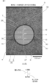
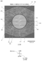
- FIG. 1 shows an image processing diagram of an SEM photograph of a vertical cross section of Example 1, which is a specific example of an embodiment of the inductor of the present invention.
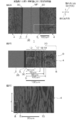
- 2A to 2C are image processing diagrams of SEM photographs of the first flat cross section of the inductor shown in FIG. 1, FIG. 2A is a view of the first flat cross section, FIG. 2B is an enlarged view of FIG. 2A, and FIG. 2C. However, an enlarged view of FIG. 2B is shown.
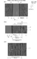
- 3A to 3C are image processing diagrams of SEM photographs of the second flat cross section of the inductor shown in FIG. 1, where FIG. 3A is a view of the second flat cross section, FIG. 3B is an enlarged view of FIG. 3A, and FIG. 3C.
- FIG. 3B An enlarged view of FIG. 3B is shown.
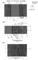
- 4A to 4C are image processing diagrams of SEM photographs of the third planar cross section of the inductor shown in FIG. 1, FIG. 4A is a view of the third planar cross section, FIG. 4B is an enlarged view of FIG. 4A, and FIG. 4C.
- FIG. 4B an enlarged view of FIG. 4B is shown.
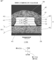
- 5A to 5C are process diagrams for explaining the manufacture of the inductor shown in FIG. 1, FIG. 5A is a process of preparing a first magnetic sheet and wiring, and FIG. 5B is a process of burying wiring in the first magnetic sheet.
- FIG. 5C show a step of sandwiching the wiring and the first magnetic sheet between the second magnetic sheet and the third magnetic sheet.
- FIG. 6 shows an image processing diagram of an SEM photograph of a vertical cross section of Example 2, which is a specific example of a modification of the inductor shown in FIG.
- FIG. 7 shows an image processing diagram of an SEM photograph of a vertical cross section of Example 3, which is a specific example of a modification of the inductor of the present invention.
- 8A to 8C are image processing diagrams of SEM photographs of the first flat cross section to the third flat cross section of the inductor shown in FIG. 7, FIG. 2A is a view of the first flat cross section, and FIG. 2B is a second flat cross section. A cross-sectional view, FIG.
- FIG. 9A to 9B are image processing diagrams of SEM photographs of the vertical cross section to the first flat cross section of Comparative Example 1, FIG. 9A shows a vertical cross section, and FIG. 9B shows a view of the first flat cross section.
- FIG. 10 shows an image processing diagram of an SEM photograph of the first flat cross section of Comparative Example 3.
- the inductor 1 has a shape extending in a plane direction orthogonal to the thickness direction (direction along the paper surface in FIGS. 2A to 4C).
- the inductor 1 has one surface 5 and the other surface 6 facing each other in the thickness direction.
- One surface 5 and the other surface 6 are substantially parallel to each other and each have a substantially flat shape.
- the inductor 1 includes a wiring 35 and a magnetic layer 4.
- a plurality of wirings 35 are provided in the inductor 1 at intervals in the plane direction when viewed in a vertical cross section 16 orthogonal to the direction along the wiring 35.
- the following description describes one wiring 35, but the same applies to the other wiring 35.
- the wiring 35 has a shape extending along one direction included in the surface direction of the inductor 1. Further, as shown in FIG. 1, the wiring 35 has a substantially circular shape when viewed in the vertical cross section 16.
- the wiring 35 includes a lead wire 2 and an insulating film 3.
- the lead wire 2 has a shape extending along the above-mentioned one direction. Further, as shown in FIG. 1, the lead wire 2 has a substantially circular shape when viewed in a vertical cross section 16 along a direction orthogonal to the flow direction (direction along the flow direction). As a result, the lead wire 2 has a lead wire circumferential surface 7 when viewed in the vertical cross section 16.
- the conducting wire 2 examples include metal conductors such as copper, silver, gold, aluminum, nickel, and alloys thereof, and copper is preferable.
- the conducting wire 2 may have a single-layer structure, or may have a multi-layer structure in which the surface of a core conductor (for example, copper) is plated (for example, nickel).
- the radius of the lead wire 2 is, for example, 25 ⁇ m or more, preferably 50 ⁇ m or more, and for example, 2000 ⁇ m or less, preferably 200 ⁇ m or less.
- the insulating film 3 protects the lead wire 2 from chemicals and water, and also prevents a short circuit between the lead wire 2 and the magnetic layer 4.
- the insulating film 3 is arranged on the peripheral surface of the conducting wire 2 when viewed in the vertical cross section 16. Specifically, the insulating film 3 covers the entire peripheral surface 7 (outer peripheral surface) of the conductive wire 2 when viewed in the vertical cross section 16. Further, the insulating film 3 has a substantially annular shape in cross section that shares the central axis (center) with the conducting wire 2. As a result, the insulating film 3 has an insulating circumferential surface 25 when viewed in the vertical cross section 16.
- Examples of the material of the insulating film 3 include insulating resins such as polyvinylformal, polyester, polyesterimide, polyamide (including nylon), polyimide, polyamideimide, and polyurethane. These may be used alone or in combination of two or more.
- insulating resins such as polyvinylformal, polyester, polyesterimide, polyamide (including nylon), polyimide, polyamideimide, and polyurethane. These may be used alone or in combination of two or more.
- the insulating film 3 may be composed of a single layer or may be composed of a plurality of layers.
- the thickness of the insulating film 3 is substantially uniform in the radial direction of the lead wire 2 at any position in the circumferential direction, for example, 1 ⁇ m or more, preferably 3 ⁇ m or more, and for example, 100 ⁇ m or less, preferably 100 ⁇ m or less. It is 50 ⁇ m or less.
- the ratio of the radius of the lead wire 2 to the thickness of the insulating film 3 is, for example, 1 or more, preferably 10 or more, and for example, 500 or less, preferably 100 or less.
- the radius of the wiring 35 is, for example, 25 ⁇ m or more, preferably 50 ⁇ m or more, and for example, 2000 ⁇ m or less, preferably 200 ⁇ m or less.
- the magnetic layer 4 improves the inductance of the inductor 1.
- Wiring 35 is embedded in the magnetic layer 4.
- the magnetic layer 4 is arranged on the peripheral surface of the insulating film 3 when viewed in the vertical cross section 16. Specifically, the magnetic layer 4 covers the entire surface of the insulating circumferential surface 25 (outer peripheral surface) of the insulating film 3.
- the magnetic layer 4 forms the outer shape of the inductor 1. Specifically, the magnetic layer 4 has a sheet shape and a rectangular shape extending in the plane direction. More specifically, the magnetic layer 4 has one surface and the other surface facing each other in the thickness direction, and one surface and the other surface of the magnetic layer 4 respectively have one surface 5 and the other surface 6 of the inductor 1. Form each of.
- the magnetic layer 4 contains anisotropic magnetic particles 8.
- the material of the magnetic layer 4 is a magnetic composition containing anisotropic magnetic particles 8 and a binder 9.
- the magnetic layer 4 is a cured product of a thermosetting resin composition (composition containing anisotropic magnetic particles 8 and a thermosetting component described later).
- Examples of the magnetic material constituting the anisotropic magnetic particles 8 include a soft magnetic material and a hard magnetic material.
- a soft magnetic material is preferably used from the viewpoint of inductance.
- the soft magnetic material examples include a single metal body containing one kind of metal element in a pure substance state, for example, one or more kinds of metal elements (first metal element) and one or more kinds of metal elements (second metal element).
- first metal element one or more kinds of metal elements
- second metal element one or more kinds of metal elements
- the single metal body examples include a single metal composed of only one kind of metal element (first metal element).
- the first metal element is appropriately selected from, for example, iron (Fe), cobalt (Co), nickel (Ni), and other metal elements that can be contained as the first metal element of the soft magnetic material. ..
- the single metal body includes, for example, a core containing only one kind of metal element and a surface layer containing an inorganic substance and / or an organic substance that modifies a part or all of the surface of the core, for example.
- examples thereof include an organic metal compound containing a first metal element and a form in which an inorganic metal compound is decomposed (thermal decomposition, etc.).
- thermal decomposition etc.
- iron powder obtained by thermally decomposing an organic iron compound (specifically, carbonyl iron) containing iron as the first metal element (sometimes referred to as carbonyl iron powder). And so on.
- the position of the layer containing the inorganic substance and / or the organic substance that modifies the portion containing only one kind of metal element is not limited to the above-mentioned surface.
- the organometallic compound or inorganic metal compound capable of obtaining a single metal body is not particularly limited, and a known or commonly used organometallic compound or inorganic metal compound capable of obtaining a soft magnetic single metal body is not particularly limited. Can be appropriately selected from.
- the alloy body is a eutectic of one or more kinds of metal elements (first metal element) and one or more kinds of metal elements (second metal element) and / or non-metal elements (carbon, nitrogen, silicon, phosphorus, etc.). It is not particularly limited as long as it is a body and can be used as an alloy body of a soft magnetic material.
- the first metal element is an essential element in the alloy body, and examples thereof include iron (Fe), cobalt (Co), and nickel (Ni). If the first metal element is Fe, the alloy body is an Fe-based alloy, and if the first metal element is Co, the alloy body is a Co-based alloy, and the first metal element is Ni. For example, the alloy body is a Ni-based alloy.
- the second metal element is an element (sub-component) secondarily contained in the alloy body, and is a metal element that is compatible (cofusable) with the first metal element.
- iron (Fe) the first. 1 When the metal element is other than Fe), Cobalt (Co) (when the first metal element is other than Co), Nickel (Ni) (when the first metal element is other than Ni), Chromium (Cr), Aluminum (Al), silicon (Si), copper (Cu), silver (Ag), manganese (Mn), calcium (Ca), barium (Ba), titanium (Ti), zirconium (Zr), ruthenium (Hf), vanadium (V), Niob (Nb), Tantal (Ta), Molybdenum (Mo), Tungsten (W), Ruthenium (Ru), Rodium (Rh), Zinc (Zn), Gallium (Ga), Indium (In), Germanium Examples thereof include (Ge), tin (Sn), lead (Pb), scandium (Sc), rut
- the non-metal element is an element (sub-component) secondarily contained in the alloy body, and is a non-metal element that is compatible (combined) with the first metal element.
- boron (B) and carbon examples thereof include (C), nitrogen (N), silicon (Si), phosphorus (P) and sulfur (S). These can be used alone or in combination of two or more.
- Fe-based alloys examples include magnetic stainless steel (Fe-Cr-Al-Si alloy) (including electromagnetic stainless steel), sentust (Fe-Si-Al alloy) (including super sentust), and permalloy (including supersendust).
- magnetic stainless steel Fe-Cr-Al-Si alloy
- sentust Fe-Si-Al alloy
- permalloy including supersendust
- Fe-Ni alloy Fe-Ni alloy
- Fe-Ni-Mo alloy Fe-Ni-Mo-Cu alloy
- Fe-Ni-Co alloy Fe-Cr alloy
- Fe-Cr-Al alloy Fe-Ni-Cr alloy
- Fe- Ni—Cr—Si alloy silicon copper (Fe—Cu—Si alloy)
- Fe—Si alloy Fe—Si—B (—Cu—Nb) alloy
- Fe—B—Si—Cr alloy Fe—Si—Cr -Ni alloy
- Fe-Si-Cr alloy Fe-Si-Al-Ni-Cr alloy
- Fe-Ni-Si-Co alloy Fe-N alloy, Fe-C alloy, Fe-B alloy, Fe-P alloy
- Ferrites stainless ferrites, Mn-Mg-based ferrites, Mn-Zn-based ferrites, Ni-Zn-based ferrites, Ni-Zn-Cu-based ferrites, Cu-Zn-based ferrites, Cu-Mg-Zn-based
- Co-based alloys examples include Co-Ta-Zr and cobalt (Co) -based amorphous alloys.
- Ni-based alloys which are examples of alloys, include Ni—Cr alloys.
- an alloy body is preferable, an Fe-based alloy is more preferable, and Sendust (Fe—Si—Al alloy) is more preferable, from the viewpoint of magnetic properties.
- the soft magnetic material preferably a single metal body, more preferably a single metal body containing an iron element in a pure substance state, still more preferably iron alone or iron powder (carbonyl iron powder). Can be mentioned.
- the shape of the anisotropic magnetic particles 8 examples include a flat shape (plate shape) and a needle shape from the viewpoint of anisotropy (or orientation), and are preferably compared to the plane direction (two-dimensional). From the viewpoint of good magnetic permeability, a flat shape can be mentioned.
- the magnetic layer 4 may further contain non-anisotropic magnetic particles in addition to the anisotropic magnetic particles 8.
- the non-anisotropic magnetic particles may have a shape such as a spherical shape, a granular shape, a lump shape, or a pellet shape.
- the average particle size of the non-anisotropic magnetic particles is, for example, 0.1 ⁇ m or more, preferably 0.5 ⁇ m or more, and for example, 200 ⁇ m or less, preferably 150 ⁇ m or less.
- the flatness (flatness) of the flat anisotropic magnetic particles 8 is, for example, 8 or more, preferably 15 or more, and for example, 500 or less, preferably 450 or less.
- the flatness is calculated as, for example, an aspect ratio obtained by dividing the average particle diameter (average length) (described later) of the anisotropic magnetic particles 8 by the average thickness of the anisotropic magnetic particles 8.
- the average particle diameter (average length) of the anisotropic magnetic particles 8 is, for example, 3.5 ⁇ m or more, preferably 10 ⁇ m or more, and for example, 200 ⁇ m or less, preferably 150 ⁇ m or less. If the anisotropic magnetic particles 8 are flat, the average thickness thereof is, for example, 0.1 ⁇ m or more, preferably 0.2 ⁇ m or more, and for example, 3.0 ⁇ m or less, preferably 2.5 ⁇ m. It is as follows.
- the proportion of the anisotropic magnetic particles 8 in the magnetic layer 4 is 40% by volume or more, preferably 45% by volume or more, more preferably 50% by volume or more, still more preferably 55% by volume or more, and particularly preferably 60. It is more than% by volume. If the ratio of the anisotropic magnetic particles 8 in the magnetic layer 4 does not meet the above lower limit, the inductor 1 cannot obtain an excellent inductance.
- the proportion of the anisotropic magnetic particles 8 in the magnetic layer 4 is, for example, 95% by volume or less, preferably 90% by volume or less.
- the proportion of the anisotropic magnetic particles 8 is equal to or less than the above upper limit, the inductor 1 has excellent mechanical strength.
- the binder 9 is a matrix in which the anisotropic magnetic particles 8 are dispersed in the magnetic layer 3. Further, the binder 9 is dispersed in the magnetic layer 3 in a predetermined direction.
- examples of the binder 9 include a thermoplastic component such as an acrylic resin, and a thermosetting component such as an epoxy resin composition.
- Acrylic resins include, for example, carboxyl group-containing acrylic acid ester copolymers.
- the epoxy resin composition contains, for example, an epoxy resin (cresol novolac type epoxy resin or the like) as a main agent, a curing agent for epoxy resin (phenol resin or the like), and a curing accelerator for epoxy resin (imidazole compound or the like).
- the binder 9 contains a cured product of a thermosetting component.
- the proportion of the binder 9 in the magnetic composition is the balance of the anisotropic magnetic particles 8.
- the anisotropic magnetic particles 8 covering the insulating circumferential surface 25 of the insulating film 3 are oriented, for example, along the circumferential direction of the conducting wire 2. Further, if the anisotropic magnetic particles 8 are flat, the anisotropic magnetic particles 8 covering the insulating circumferential surface 25 are oriented in the circumferential direction when the magnetic layer 4 is viewed in the vertical cross section 16.
- the first flat cross section 11, the second flat cross section 12, and the third flat cross section 13 are defined as follows.
- the first flat cross section 11 is a central flat cross section that passes through the midpoint MP of the line segment L connecting the one end edge 36 and the other end edge 37 in the thickness direction of the lead wire 2.
- the first flat cross section 11 is along the plane direction of the inductor 1. Specifically, the first flat cross section 11 is substantially parallel to at least the other surface 6 in the thickness direction of the inductor 1.
- the second flat cross section 12 is a flat cross section that passes through the first point P1 located at a position where the length (1/4 L) of 1/4 of the line segment L is advanced from the midpoint MP to one side in the thickness direction.
- the second flat cross section 12 is along the plane direction of the inductor 1. Specifically, the second flat cross section 12 is parallel to the first flat cross section 11.
- the third flat cross section 13 is the other flat cross section that passes through the second point P2 at a position where the length (1 / 4L) is advanced from the midpoint MP to the other side in the thickness direction.
- the third flat cross section 33 is along the plane direction of the inductor 1. Specifically, the third flat cross section 33 is parallel to the first flat cross section 11.
- the neighboring region 10 and the outer region 20 are arranged in this order in the first direction (corresponding to the left-right direction of FIGS. .
- the insulating film 3 is arranged in order from the outer edge 30 toward the outside in the first direction, and there is no gap between the neighboring region 10 and the outer region 20 and they are continuous with each other.
- the vicinity region 10 is a region within 50 ⁇ m outward from the outer edge 30 of the insulating film 3 in the first direction in the first direction, and is a band-shaped region along the flow direction. Further, the vicinity region 10 is a portion that has a stronger influence on the inductance of the inductor 1 than the outer region 20 described below.
- the outer region 20 has a first outer region 17, a second outer region 18, and a third outer region 19.
- the first outer region 17, the second outer region 18, and the third outer region 19 are arranged in parallel in this order toward the outside in the first direction.
- the first outer region 17 is adjacent to the outer side of the neighboring region 10 in the first direction. Specifically, the first outer region 17 is a region within 75 ⁇ m in excess of 50 ⁇ m from the outer edge 30 in the first direction of the insulating film 3 in the first direction, and is a band-shaped region along the flow direction. .. That is, the first outer region 17 is a region within 25 ⁇ m from the outer edge of the neighboring region 10 in the first direction.
- the second outer region 18 is adjacent to the outer side of the first outer region 17 in the first direction.
- the second outer region 18 is a region that is more than 75 ⁇ m and 95 ⁇ m or less outward from the outer edge 30 of the insulating film 3 in the first direction in the first direction, and is a band-shaped region along the flow direction. .. That is, the second outer region 18 is a region within 20 ⁇ m from the outer edge of the first outer region 17 in the first direction.
- the third outer region 19 is adjacent to the outer side of the second outer region 18 in the first direction.
- the third outer region 19 is a region that is more than 95 ⁇ m and 105 ⁇ m or less outward from the outer edge 30 of the insulating film 3 in the first direction in the first direction, and is a band-shaped region along the flow direction. .. That is, the third outer region 19 is a region within 10 ⁇ m from the outer edge of the second outer region 18 in the first direction.
- the anisotropic magnetic particles 8 are electrically in the vicinity region 10 at least.
- An orientation region oriented in a substantially linear shape along the flow direction is observed.
- the anisotropic magnetic particles 8 are oriented in the flow direction.
- the case where the above angle exceeds 15 degrees is defined as "the anisotropic magnetic particles 8 are not oriented in the flow direction”.
- the orientation region is the sum of the number of anisotropic magnetic particles 8 oriented in the flow direction, the number of anisotropic magnetic particles 8 oriented in the flow direction, and the number of anisotropic magnetic particles 8 not oriented in the flow direction. It is a region in which the ratio with respect to 50% is more than 50%, preferably 60% or more, more preferably 70% or more, still more preferably 75% or more, and particularly preferably 80% or more.
- the orientation region is observed in the vicinity region 10 and the first outer region 17 when viewed in any of the first flat cross section 11, the second flat cross section 12, and the third flat cross section 13.
- first flat cross section 11 or second flat cross section 12 of the first flat cross section 11, the second flat cross section 12, and the third flat cross section 13, and two more. Orientation regions are observed in the neighborhood region 10, the first outer region 17, and the second outer region 18 when viewed in planographic sections (eg, first flat section 11 and second flat section 12).
- the orientation region when viewed in one flat section (specifically, the first flat cross section 11) of the first flat cross section 11, the second flat cross section 12, and the third flat cross section 13, the orientation region is It is observed in the vicinity region 10, the first outer region 17, the second outer region 18, and the third outer region 19.
- the orientation regions are the neighborhood region 10 and the first outer region 17 when viewed in the first flat cross section 11, as referred to the first column of Example 2 in Table 2.
- the second outer region 18 and the third outer region 19 are observed.
- the orientation region is observed in the neighboring region 10, the first outer region 17 and the second outer region 18, while the third outer region 19 is observed.
- the orientation region is observed in the neighborhood region 10 and the first outer region 17, while the second outer region 18 and the third outer region 19 are observed.
- the orientation region is observed in both the near region 10 and the outer region 20.
- the anisotropic magnetic particles 8 are oriented along the flow direction, and the vertical cross section 16 is formed.
- the lead wire 2 is oriented along the circumferential direction.
- the aspect ratio of the anisotropic magnetic particle 8 itself is 100
- the aspect ratio observed in the first flat cross section 11 specifically, the aspect ratio of the anisotropic magnetic particle 8 in the above-mentioned cross-sectional view (vertical direction).
- the length l / lateral length w) is, for example, 50 or more, preferably 75 or more
- the anisotropic magnetic particle 8 has a flow direction and a flow direction. It can be defined as being oriented along the circumferential direction of the lead wire 2.
- the anisotropic magnetic particles 8 are oriented in both the flow direction and the circumferential direction, a magnetic path that surrounds the conducting wire 2 and follows the flow of electricity is formed in the magnetic layer 4, whereby the inductor 1 of the inductor 1 is formed.
- the inductance can be improved.
- the orientation region when viewed in the first flat cross section 11, the second flat cross section 12, and the third flat cross section 13, the orientation region may be observed in the outer region 20 and also in the portion outside the third outer region 19. Or, it does not have to be observed.
- the intersection (top) 50 is formed by two types of anisotropic magnetic particles 8 having different orientation directions.
- the intersection 50 is located on the other side in the thickness direction from the third flat cross section 13.
- the intersection 50 passes through the other end edge 37 of the lead wire 2 and is located on one side in the thickness direction of the fifth cross section (not shown) parallel to the third flat cross section 13. That is, the intersection 50 is located between the third cross section 13 and the fifth cross section (not shown).
- the thickness of the magnetic layer 4 is, for example, twice or more, preferably three times or more, and for example, 20 times or less the radius of the lead wire 2. Specifically, the thickness of the magnetic layer 4 is, for example, 100 ⁇ m or more, preferably 200 ⁇ m or more, and for example, 2000 ⁇ m or less, preferably 1000 ⁇ m or less. The thickness of the magnetic layer 4 is the distance between one surface 5 and the other surface 6 of the magnetic layer 4.
- the thickness of the inductor 1 is the same as the thickness of the magnetic layer 4 described above.
- the wiring 35 is first prepared, the magnetic sheet 24 is prepared, and then, as shown in FIG. 5B, the wiring 35 is connected by the magnetic sheet 24.
- the magnetic layer 4 is formed by burying them together.
- the magnetic sheet 24 may be one sheet, or may include a plurality of sheets. Specifically, the magnetic sheet 24 includes at least the first magnetic sheet 21 (FIG. 5A), preferably the first magnetic sheet 21, the second magnetic sheet 22 (FIG. 5B), and the third magnetic sheet 23 (FIG. 5B). 5B) is included separately.
- Each material of the first magnetic sheet 21, the second magnetic sheet 22, and the third magnetic sheet 23 contains the above-mentioned anisotropic magnetic particles 8 and the binder 9, and has a sheet shape extending in the plane direction.
- Each of the first magnetic sheet 21, the second magnetic sheet 22, and the third magnetic sheet 23 is preferably prepared as a B stage sheet.
- Each of the first magnetic sheet 21, the second magnetic sheet 22, and the third magnetic sheet 23 may be a single layer, or may be a multilayer (specifically, the inner sheet and the lead wire 2 with respect to the inner sheet. It may be composed of an outer sheet located on the opposite side of the.
- Examples of the first magnetic sheet 21, the second magnetic sheet 22, and the third magnetic sheet 23 include soft magnetic thermosetting adhesive films described in JP-A-2014-165363, JP-A-2015-92544, and the like. ..
- the wiring 35 is embedded by the first magnetic sheet 21 shown by the solid line (preferably, the wiring 35 is heat-pressed). As a result, the intersection 50 is formed on the first magnetic sheet 21.
- the second magnetic sheet 22 and the third magnetic sheet 23 are sandwiched between the wiring 35 and the first magnetic sheet 21 in the thickness direction to form the first magnetic sheet.
- the sheet 21 is arranged on one side and the other side in the thickness direction (preferably heat-pressed). As a result, the magnetic layer 4 having one surface 5 and the other surface 6 is formed.
- the magnetic layer 4 is in the B stage, it is converted into the C stage.
- FIG. 5C shows the boundary between the first magnetic sheet 21 and the second magnetic sheet 22 and the boundary between the first magnetic sheet 21 and the third magnetic sheet 23, but as can be seen from the SEM photograph of FIG. They may be ambiguous.
- the region 10 an orientation region in which the anisotropic magnetic particles 8 are oriented in the flow direction is observed. Therefore, in the vicinity region 10, a magnetic path along the flow direction is formed.
- the conducting wire 2 has the guiding wire circumferential surface 7 when viewed in a vertical cross section, the anisotropic magnetic particles 8 are oriented in the flow direction in the magnetic layer 4 facing the guiding wire circumferential surface 7. easy.
- the magnetic layer 4 contains 40% by volume or more of the anisotropic magnetic particles 8.
- this inductor 1 has excellent inductance.
- the inductor 1 of this embodiment when the magnetic layer 4 is viewed in each of the first flat cross section 11, the second flat cross section 12, and the third flat cross section 13, the orientation region is located in the vicinity region 10. As observed, the inductor 1 is even better due to the inductance.
- the plane direction of the anisotropic magnetic particles 8 is oriented in the circumferential direction of the lead wire 2. Therefore, a magnetic path surrounding the lead wire 2 is formed. As a result, the inductance is even better.
- the orientation region is observed in any of the neighboring regions 10 of the first flat cross section 11, the second flat cross section 12 and the third flat cross section 13. To.
- the cross section in which the orientation region is observed is not limited to all (three) of the above three, and may be two.
- the alignment region is observed in the neighborhood region 10 (furthermore, the first outer region 17 and the second outer region 18), while the orientation region is the neighborhood region when viewed in the first flat cross section 11. Not observed at 10.
- the intersection 50 is located on, for example, the first flat cross section 11.
- the orientation region is observed in the vicinity region 10 in the second flat cross section 12 and the third flat cross section 13.
- two of the three flat cross sections are not limited to the above-mentioned second flat cross section 12 and third flat cross section 13, but the first flat cross section 11 and the second flat cross section 12 (FIGS. 7 to 8C described later). (See), or it may be either the first flat cross section 11 or the third flat cross section 13.
- the orientation region is the neighborhood region 10 when viewed in the third flat cross section 13. Not observed in. Further, when the alignment region is observed in the vicinity region 10 when viewed in the first flat cross section 11 and the third plane cross section 13, the orientation region is the neighborhood region 10 when viewed in the second flat cross section 12. Not observed in.
- the orientation region is located in the vicinity region 10.
- the inductor 1 of the embodiment shown in FIGS. 1 to 4C is more excellent in inductance than the modified example inductor 1 shown in FIGS. 6 to 7C.
- the wiring 35 and the lead wire 2 have a substantially circular shape when viewed in the vertical cross section 16, but, for example, as shown in FIG. 7, they have a substantially rectangular shape. There may be.
- This inductor 1 includes a conductor pattern 38 as an example of a conducting wire, an insulating film 3, and a magnetic layer 4.
- the inductor 1 is a modification in which the orientation region is observed in the vicinity region 10 in the first flat cross section 11 and the second flat cross section 12, which are two of the three flat cross sections.
- the conductor pattern 38 includes one surface 39 and the other surface 40 facing in the thickness direction and two connecting surfaces 41 connecting both ends of the one surface 39 and the other surface 40 in the first direction when viewed in the vertical cross section 16. Is provided integrally.
- Each of the one surface 39 and the other surface 40 is a flat surface and is parallel to each other.
- the insulating film 3 may cover the entire outer peripheral surface of the lead wire 2.
- the conductor pattern 38 has two corners 42 formed by one surface 39 and a connecting surface 41, and each of the two corners 42 constitutes a curved portion (curved surface).
- the radius of curvature of the curved surface of the corner 42 is, for example, 5 ⁇ m or more and 30 ⁇ m or less.
- the thickness of the conductor pattern 38 is the distance between the one surface 39 and the other surface 40.
- the width of the conductor pattern 38 is the average distance between the two connecting surfaces 41, and is, for example, 20 ⁇ m or more and 1000 ⁇ m or less.
- the insulating film 3 is arranged on one surface 39, the other surface 40, and the connecting surface 41 of the conductor pattern 38.
- the magnetic layer 4 has a first magnetic layer 45 and a second magnetic layer 46.
- the first magnetic layer 45 has a substantially plate shape extending in the plane direction.
- the material of the first magnetic layer 45 is the above-mentioned magnetic composition.
- the anisotropic magnetic particles 8 are oriented in the flow direction and the plane direction.
- the second magnetic layer 46 has a sheet shape extending in the plane direction. One surface of the second magnetic layer 46 in the thickness direction is exposed toward one side in the thickness direction, and the other surface of the second magnetic layer 46 covers one surface 39 of the conductor pattern 38 and the connecting surface 41, and is a conductor. It is in contact with one surface of the first magnetic layer 45 exposed from the pattern 38.
- the anisotropic magnetic particles 8 facing the one surface 39 are oriented in the plane direction and the flow direction, and the anisotropic magnetic particles 8 facing the connecting surface 41 have a thickness as described later.
- the anisotropic magnetic particles 8 that are oriented along the direction and the flow direction and that face the corner portion 42 are oriented along the circumferential direction and the flow direction centered on the corner portion 42.
- the corner portion 42 of the conductor pattern 38 does not have to have a curved portion, that is, a curved surface.
- the corner 42 is a bent portion that bends at, for example, 45 degrees or more, 60 degrees or more, 75 degrees or more, and for example, 135 degrees or less, 120 degrees or less, 105 degrees or less (more specifically, 90 degrees). There may be.
- the inductor 1 includes a plurality of wirings 35, but for example, one wiring 35 can also be provided.
- the definition of the vicinity region 10 is expressed using the absolute distance from the outer edge 30 in the first direction, but it can also be expressed using the relative distance.
- the anisotropic magnetic particle 8 is flat. If this is the case, it can be defined as a region within 0.08 with respect to the average thickness of the anisotropic magnetic particles 8 from the outer edge 30 in the first direction to the outside in the first direction. That is, the ratio of the above-mentioned distance to the average thickness of the anisotropic magnetic particles 8 can be 0.08.
- the first outer region 17 can be defined as a region exceeding 0.08 and within 0.13 from the outer edge 30 in the first direction to the outside in the first direction, and is the second outer region.
- the region 18 can be defined as a region exceeding 0.13 and within 0.175 from the outer edge 30 in the first direction, and the third outer region 19 is outside the outer edge 30 in the first direction in the first direction. Can be defined as a region greater than 0.175 and within 0.225.
- the proportion of the anisotropic magnetic particles 8 in the magnetic layer 4 may be uniform in the magnetic layer 4, and may be increased or decreased as the distance from each wiring 2 increases.
- the proportion of the anisotropic magnetic particles 8 in the magnetic layer 4 increases as the distance from the wiring 35 increases, for example, as shown in FIG. 5B, the anisotropic magnetic particles in the second magnetic sheet 22.
- the abundance ratio of 8 and the abundance ratio of the anisotropic magnetic particles 8 on the third magnetic sheet 23 are set higher than the abundance ratio of the anisotropic magnetic particles 8 on the first magnetic sheet 21.
- Examples and comparative examples are shown below, and the present invention will be described in more detail.
- the present invention is not limited to Examples and Comparative Examples.
- specific numerical values such as the compounding ratio (content ratio), physical property values, and parameters used in the following description are the compounding ratios corresponding to those described in the above-mentioned "Form for carrying out the invention".
- Content ratio can be replaced with the upper limit (numerical value defined as “less than or equal to” or “less than”) or lower limit (numerical value defined as "greater than or equal to” or “excess”). it can.
- Example 1 Example drawn in FIGS. 1 to 4C ⁇ Inductor based on one embodiment> The inductor 1 was manufactured based on one embodiment. Specifically, a wiring 35 including a lead wire 2 made of copper having a radius of 100 ⁇ m and an insulating film 3 having a thickness of 10 ⁇ m was prepared. Separately, the first magnetic sheet 21 was prepared as a B stage sheet. The layer structure and formulation of the first magnetic sheet 21 are shown in Table 1.
- the first magnetic sheet 21 was then attached (heat pressed) to the wiring 35.
- the second magnetic sheet 22 and the third magnetic sheet 23 were prepared as B stage sheets.
- the layer structure and formulation of the second magnetic sheet 22 and the third magnetic sheet 23 are shown in Table 1.
- the wiring 35 and the first magnetic sheet 21 were sandwiched between the second magnetic sheet 22 and the third magnetic sheet 23, and they were attached (heat pressed).
- thermosetting components in the first magnetic sheet 21, the second magnetic sheet 22, and the third magnetic sheet 23 were C-staged.
- the wiring 35 is embedded by the magnetic layer 4 composed of the first magnetic sheet 21, the second magnetic sheet 22, and the third magnetic sheet 23 of the C stage, and as shown in FIG. 1, the wiring 35 and the magnetic layer 4 An inductor 1 comprising the above was manufactured.
- the obtained inductor 1 was subjected to SEM observation of each of the vertical cross section 16, the first flat cross section 11, the second flat cross section 12, and the third flat cross section 13, and an attempt was made to observe the orientation region.
- the image processing diagrams are shown in FIGS. 1 to 4C, and the observation results of the orientation region are shown in Table 2.
- Example 2 Example drawn in FIG. 6 ⁇ Example of manufacturing an inductor based on a modified example of one embodiment> The inductor 1 shown in FIG. 6 was obtained in the same manner as in the first embodiment except that the wiring 35 was sandwiched between the second magnetic sheet 22 and the third magnetic sheet 23 without using the first magnetic sheet 21. SEM observations of the plan surface 11, the second flat section 12, and the third flat section 13 were carried out.
- Table 2 shows the observation results of the orientation region.
- Example 3 Example drawn in FIGS. 7 to 8C ⁇ Example of manufacturing an inductor based on a modified example of one embodiment>
- the cross-sectional area (regular cross-sectional area) in the vertical cross section 16 is the same as that in the first embodiment, but the inductor 1 is obtained in the same manner as in the first embodiment except that the substantially rectangular conducting wire 2 is used. SEM observations of the cross section 11, the second flat cross section 12, and the third flat cross section 13 were carried out.
- the lead wire 2 was covered with the B stage sheet via the insulating film 3.
- Table 2 shows the observation results of the orientation region.
- Comparative Example 1 Example drawn in FIGS. 9A to 9B Inductor 1 in the same manner as in Example 2 in which the second magnetic sheet 22 and the third magnetic sheet 23 at the time of bonding to the wiring 35 are changed to a cured body of the C stage.
- the SEM observations of the first flat cross section 11, the second flat cross section 12, and the third flat cross section 13 were carried out.
- Table 3 shows the observation results of the orientation region.
- Comparative Example 2 An inductor 1 was obtained in the same manner as in Example 3 in which the second magnetic sheet 22 and the third magnetic sheet 23 at the time of bonding were changed to a cured body of the C stage, and the first flat cross section 11 and the second flat cross section 12 were obtained. And each SEM observation of the third plane cross section 13 was carried out.
- Table 3 shows the observation results of the orientation region.
- Comparative Example 3 Example drawn in FIG. 10
- the inductor 1 is the same as in Example 11 except that spherical magnetic particles (average particle diameter 20 ⁇ m, Fe—Si—Al alloy) are used instead of the anisotropic magnetic particles 8.
- spherical magnetic particles average particle diameter 20 ⁇ m, Fe—Si—Al alloy
- Table 3 shows the observation results of the orientation region.
- the inductor is mounted on, for example, an electronic device.
Landscapes
- Engineering & Computer Science (AREA)
- Power Engineering (AREA)
- Chemical & Material Sciences (AREA)
- Dispersion Chemistry (AREA)
- Microelectronics & Electronic Packaging (AREA)
- Physics & Mathematics (AREA)
- Spectroscopy & Molecular Physics (AREA)
- Coils Or Transformers For Communication (AREA)
- Soft Magnetic Materials (AREA)
Priority Applications (3)
| Application Number | Priority Date | Filing Date | Title |
|---|---|---|---|
| KR1020217028621A KR102852328B1 (ko) | 2019-03-12 | 2020-02-05 | 인덕터 |
| US17/437,663 US20220165481A1 (en) | 2019-03-12 | 2020-02-05 | Inductor |
| CN202080016827.5A CN113474856B (zh) | 2019-03-12 | 2020-02-05 | 电感器 |
Applications Claiming Priority (2)
| Application Number | Priority Date | Filing Date | Title |
|---|---|---|---|
| JP2019-044778 | 2019-03-12 | ||
| JP2019044778A JP7362269B2 (ja) | 2019-03-12 | 2019-03-12 | インダクタ |
Publications (1)
| Publication Number | Publication Date |
|---|---|
| WO2020183993A1 true WO2020183993A1 (ja) | 2020-09-17 |
Family
ID=72426223
Family Applications (1)
| Application Number | Title | Priority Date | Filing Date |
|---|---|---|---|
| PCT/JP2020/004232 WO2020183993A1 (ja) | 2019-03-12 | 2020-02-05 | インダクタ |
Country Status (6)
Cited By (2)
| Publication number | Priority date | Publication date | Assignee | Title |
|---|---|---|---|---|
| CN115116694A (zh) * | 2021-03-17 | 2022-09-27 | 株式会社村田制作所 | 电感器部件及其制造方法 |
| JP2022184542A (ja) * | 2021-06-01 | 2022-12-13 | 株式会社村田製作所 | インダクタ部品およびその製造方法 |
Citations (2)
| Publication number | Priority date | Publication date | Assignee | Title |
|---|---|---|---|---|
| JP2001185421A (ja) * | 1998-12-28 | 2001-07-06 | Matsushita Electric Ind Co Ltd | 磁性素子およびその製造方法 |
| JP2017037888A (ja) * | 2015-08-07 | 2017-02-16 | 国立大学法人信州大学 | 磁性粉モールドコイル及びその製造方法 |
Family Cites Families (5)
| Publication number | Priority date | Publication date | Assignee | Title |
|---|---|---|---|---|
| JPH10144526A (ja) | 1996-11-05 | 1998-05-29 | Murata Mfg Co Ltd | 積層チップインダクタ |
| JP5054445B2 (ja) * | 2007-06-26 | 2012-10-24 | スミダコーポレーション株式会社 | コイル部品 |
| JP6456729B2 (ja) * | 2015-03-09 | 2019-01-23 | 株式会社トーキン | インダクタ素子およびその製造方法 |
| KR101719908B1 (ko) * | 2015-07-01 | 2017-03-24 | 삼성전기주식회사 | 코일 전자부품 및 그 제조방법 |
| KR101832564B1 (ko) * | 2015-10-27 | 2018-02-26 | 삼성전기주식회사 | 코일 부품 |
-
2019
- 2019-03-12 JP JP2019044778A patent/JP7362269B2/ja active Active
-
2020
- 2020-02-05 US US17/437,663 patent/US20220165481A1/en active Pending
- 2020-02-05 KR KR1020217028621A patent/KR102852328B1/ko active Active
- 2020-02-05 CN CN202080016827.5A patent/CN113474856B/zh active Active
- 2020-02-05 WO PCT/JP2020/004232 patent/WO2020183993A1/ja active Application Filing
- 2020-02-17 TW TW109104965A patent/TWI845611B/zh active
Patent Citations (2)
| Publication number | Priority date | Publication date | Assignee | Title |
|---|---|---|---|---|
| JP2001185421A (ja) * | 1998-12-28 | 2001-07-06 | Matsushita Electric Ind Co Ltd | 磁性素子およびその製造方法 |
| JP2017037888A (ja) * | 2015-08-07 | 2017-02-16 | 国立大学法人信州大学 | 磁性粉モールドコイル及びその製造方法 |
Cited By (5)
| Publication number | Priority date | Publication date | Assignee | Title |
|---|---|---|---|---|
| CN115116694A (zh) * | 2021-03-17 | 2022-09-27 | 株式会社村田制作所 | 电感器部件及其制造方法 |
| JP2022143415A (ja) * | 2021-03-17 | 2022-10-03 | 株式会社村田製作所 | インダクタ部品およびその製造方法 |
| JP7424331B2 (ja) | 2021-03-17 | 2024-01-30 | 株式会社村田製作所 | インダクタ部品およびその製造方法 |
| JP2022184542A (ja) * | 2021-06-01 | 2022-12-13 | 株式会社村田製作所 | インダクタ部品およびその製造方法 |
| JP7531085B2 (ja) | 2021-06-01 | 2024-08-09 | 株式会社村田製作所 | インダクタ部品およびその製造方法 |
Also Published As
| Publication number | Publication date |
|---|---|
| JP7362269B2 (ja) | 2023-10-17 |
| CN113474856B (zh) | 2025-04-29 |
| CN113474856A (zh) | 2021-10-01 |
| US20220165481A1 (en) | 2022-05-26 |
| JP2020150065A (ja) | 2020-09-17 |
| KR20210137030A (ko) | 2021-11-17 |
| KR102852328B1 (ko) | 2025-08-28 |
| TW202101487A (zh) | 2021-01-01 |
| TWI845611B (zh) | 2024-06-21 |
Similar Documents
| Publication | Publication Date | Title |
|---|---|---|
| TWI875733B (zh) | 電感器 | |
| WO2020183993A1 (ja) | インダクタ | |
| WO2020183992A1 (ja) | インダクタ | |
| US20250014795A1 (en) | Inductor | |
| JP7398197B2 (ja) | インダクタの製造方法 | |
| WO2020183994A1 (ja) | インダクタ | |
| WO2020183995A1 (ja) | インダクタ | |
| WO2020183990A1 (ja) | インダクタ | |
| WO2020183989A1 (ja) | インダクタ | |
| WO2020183998A1 (ja) | インダクタおよびその製造方法 | |
| KR20220045148A (ko) | 인덕터 |
Legal Events
| Date | Code | Title | Description |
|---|---|---|---|
| 121 | Ep: the epo has been informed by wipo that ep was designated in this application |
Ref document number: 20770208 Country of ref document: EP Kind code of ref document: A1 |
|
| NENP | Non-entry into the national phase |
Ref country code: DE |
|
| 122 | Ep: pct application non-entry in european phase |
Ref document number: 20770208 Country of ref document: EP Kind code of ref document: A1 |