WO2020183993A1 - Inductor - Google Patents
Inductor Download PDFInfo
- Publication number
- WO2020183993A1 WO2020183993A1 PCT/JP2020/004232 JP2020004232W WO2020183993A1 WO 2020183993 A1 WO2020183993 A1 WO 2020183993A1 JP 2020004232 W JP2020004232 W JP 2020004232W WO 2020183993 A1 WO2020183993 A1 WO 2020183993A1
- Authority
- WO
- WIPO (PCT)
- Prior art keywords
- section
- flat cross
- region
- inductor
- cross
- Prior art date
Links
- 239000006249 magnetic particle Substances 0.000 claims abstract description 69
- WABPQHHGFIMREM-UHFFFAOYSA-N lead(0) Chemical compound [Pb] WABPQHHGFIMREM-UHFFFAOYSA-N 0.000 claims description 31
- 230000002093 peripheral effect Effects 0.000 claims description 8
- 239000004020 conductor Substances 0.000 abstract description 17
- 239000010410 layer Substances 0.000 description 65
- 229910045601 alloy Inorganic materials 0.000 description 43
- 239000000956 alloy Substances 0.000 description 43
- 229910052751 metal Inorganic materials 0.000 description 40
- 239000002184 metal Substances 0.000 description 33
- XEEYBQQBJWHFJM-UHFFFAOYSA-N Iron Chemical compound [Fe] XEEYBQQBJWHFJM-UHFFFAOYSA-N 0.000 description 19
- PXHVJJICTQNCMI-UHFFFAOYSA-N Nickel Chemical compound [Ni] PXHVJJICTQNCMI-UHFFFAOYSA-N 0.000 description 17
- 238000010586 diagram Methods 0.000 description 11
- 239000000696 magnetic material Substances 0.000 description 10
- 239000000203 mixture Substances 0.000 description 9
- 229910000859 α-Fe Inorganic materials 0.000 description 8
- 239000011230 binding agent Substances 0.000 description 7
- 230000000052 comparative effect Effects 0.000 description 7
- 230000004048 modification Effects 0.000 description 7
- 238000012986 modification Methods 0.000 description 7
- 239000000126 substance Substances 0.000 description 7
- IJGRMHOSHXDMSA-UHFFFAOYSA-N Atomic nitrogen Chemical compound N#N IJGRMHOSHXDMSA-UHFFFAOYSA-N 0.000 description 6
- 239000010949 copper Substances 0.000 description 6
- 239000003822 epoxy resin Substances 0.000 description 6
- 229920000647 polyepoxide Polymers 0.000 description 6
- 229920001187 thermosetting polymer Polymers 0.000 description 6
- RYGMFSIKBFXOCR-UHFFFAOYSA-N Copper Chemical compound [Cu] RYGMFSIKBFXOCR-UHFFFAOYSA-N 0.000 description 5
- 229910052802 copper Inorganic materials 0.000 description 5
- 239000000463 material Substances 0.000 description 5
- 229910052759 nickel Inorganic materials 0.000 description 5
- XUIMIQQOPSSXEZ-UHFFFAOYSA-N Silicon Chemical compound [Si] XUIMIQQOPSSXEZ-UHFFFAOYSA-N 0.000 description 4
- 229910017052 cobalt Inorganic materials 0.000 description 4
- 239000010941 cobalt Substances 0.000 description 4
- GUTLYIVDDKVIGB-UHFFFAOYSA-N cobalt atom Chemical compound [Co] GUTLYIVDDKVIGB-UHFFFAOYSA-N 0.000 description 4
- 238000004519 manufacturing process Methods 0.000 description 4
- 150000002736 metal compounds Chemical class 0.000 description 4
- 238000000034 method Methods 0.000 description 4
- 239000002245 particle Substances 0.000 description 4
- 229910052710 silicon Inorganic materials 0.000 description 4
- 239000010703 silicon Substances 0.000 description 4
- OKTJSMMVPCPJKN-UHFFFAOYSA-N Carbon Chemical compound [C] OKTJSMMVPCPJKN-UHFFFAOYSA-N 0.000 description 3
- 229910018487 Ni—Cr Inorganic materials 0.000 description 3
- OAICVXFJPJFONN-UHFFFAOYSA-N Phosphorus Chemical compound [P] OAICVXFJPJFONN-UHFFFAOYSA-N 0.000 description 3
- KJTLSVCANCCWHF-UHFFFAOYSA-N Ruthenium Chemical compound [Ru] KJTLSVCANCCWHF-UHFFFAOYSA-N 0.000 description 3
- 229910002796 Si–Al Inorganic materials 0.000 description 3
- 229910008458 Si—Cr Inorganic materials 0.000 description 3
- 229910052799 carbon Inorganic materials 0.000 description 3
- 229910052757 nitrogen Inorganic materials 0.000 description 3
- 229910052755 nonmetal Inorganic materials 0.000 description 3
- 229910052698 phosphorus Inorganic materials 0.000 description 3
- 239000011574 phosphorus Substances 0.000 description 3
- 229910052707 ruthenium Inorganic materials 0.000 description 3
- 239000002356 single layer Substances 0.000 description 3
- 239000004925 Acrylic resin Substances 0.000 description 2
- 229920000178 Acrylic resin Polymers 0.000 description 2
- BQCADISMDOOEFD-UHFFFAOYSA-N Silver Chemical compound [Ag] BQCADISMDOOEFD-UHFFFAOYSA-N 0.000 description 2
- 229910052782 aluminium Inorganic materials 0.000 description 2
- XAGFODPZIPBFFR-UHFFFAOYSA-N aluminium Chemical compound [Al] XAGFODPZIPBFFR-UHFFFAOYSA-N 0.000 description 2
- 239000011575 calcium Substances 0.000 description 2
- 239000003795 chemical substances by application Substances 0.000 description 2
- 239000011651 chromium Substances 0.000 description 2
- 238000013329 compounding Methods 0.000 description 2
- 230000005611 electricity Effects 0.000 description 2
- 230000005496 eutectics Effects 0.000 description 2
- 238000009472 formulation Methods 0.000 description 2
- RAXXELZNTBOGNW-UHFFFAOYSA-N imidazole Natural products C1=CNC=N1 RAXXELZNTBOGNW-UHFFFAOYSA-N 0.000 description 2
- 229910052742 iron Inorganic materials 0.000 description 2
- 239000011572 manganese Substances 0.000 description 2
- 150000002902 organometallic compounds Chemical class 0.000 description 2
- 230000000704 physical effect Effects 0.000 description 2
- -1 polyvinylformal Polymers 0.000 description 2
- 229910052709 silver Inorganic materials 0.000 description 2
- 239000004332 silver Substances 0.000 description 2
- 229910001220 stainless steel Inorganic materials 0.000 description 2
- 239000010935 stainless steel Substances 0.000 description 2
- 239000010936 titanium Substances 0.000 description 2
- 239000011701 zinc Substances 0.000 description 2
- QTWJRLJHJPIABL-UHFFFAOYSA-N 2-methylphenol;3-methylphenol;4-methylphenol Chemical compound CC1=CC=C(O)C=C1.CC1=CC=CC(O)=C1.CC1=CC=CC=C1O QTWJRLJHJPIABL-UHFFFAOYSA-N 0.000 description 1
- 229910021364 Al-Si alloy Inorganic materials 0.000 description 1
- 229910000521 B alloy Inorganic materials 0.000 description 1
- ZOXJGFHDIHLPTG-UHFFFAOYSA-N Boron Chemical compound [B] ZOXJGFHDIHLPTG-UHFFFAOYSA-N 0.000 description 1
- OYPRJOBELJOOCE-UHFFFAOYSA-N Calcium Chemical compound [Ca] OYPRJOBELJOOCE-UHFFFAOYSA-N 0.000 description 1
- VYZAMTAEIAYCRO-UHFFFAOYSA-N Chromium Chemical compound [Cr] VYZAMTAEIAYCRO-UHFFFAOYSA-N 0.000 description 1
- 229910020516 Co—V Inorganic materials 0.000 description 1
- 229910019819 Cr—Si Inorganic materials 0.000 description 1
- 229910017518 Cu Zn Inorganic materials 0.000 description 1
- 229910017758 Cu-Si Inorganic materials 0.000 description 1
- 229910017752 Cu-Zn Inorganic materials 0.000 description 1
- 229910017931 Cu—Si Inorganic materials 0.000 description 1
- 229910017943 Cu—Zn Inorganic materials 0.000 description 1
- 229910017061 Fe Co Inorganic materials 0.000 description 1
- 229910017060 Fe Cr Inorganic materials 0.000 description 1
- 229910002544 Fe-Cr Inorganic materials 0.000 description 1
- 229910002060 Fe-Cr-Al alloy Inorganic materials 0.000 description 1
- 229910017082 Fe-Si Inorganic materials 0.000 description 1
- 229910017112 Fe—C Inorganic materials 0.000 description 1
- 229910017133 Fe—Si Inorganic materials 0.000 description 1
- GYHNNYVSQQEPJS-UHFFFAOYSA-N Gallium Chemical compound [Ga] GYHNNYVSQQEPJS-UHFFFAOYSA-N 0.000 description 1
- 229910001030 Iron–nickel alloy Inorganic materials 0.000 description 1
- PWHULOQIROXLJO-UHFFFAOYSA-N Manganese Chemical compound [Mn] PWHULOQIROXLJO-UHFFFAOYSA-N 0.000 description 1
- ZOKXTWBITQBERF-UHFFFAOYSA-N Molybdenum Chemical compound [Mo] ZOKXTWBITQBERF-UHFFFAOYSA-N 0.000 description 1
- 229910017315 Mo—Cu Inorganic materials 0.000 description 1
- 229910001199 N alloy Inorganic materials 0.000 description 1
- 229910017709 Ni Co Inorganic materials 0.000 description 1
- 229910000990 Ni alloy Inorganic materials 0.000 description 1
- 229910003267 Ni-Co Inorganic materials 0.000 description 1
- 229910003296 Ni-Mo Inorganic materials 0.000 description 1
- 229910003262 Ni‐Co Inorganic materials 0.000 description 1
- 229910018605 Ni—Zn Inorganic materials 0.000 description 1
- 239000004677 Nylon Substances 0.000 description 1
- 229910001096 P alloy Inorganic materials 0.000 description 1
- 239000004952 Polyamide Substances 0.000 description 1
- 239000004962 Polyamide-imide Substances 0.000 description 1
- 239000004642 Polyimide Substances 0.000 description 1
- 229910018598 Si-Co Inorganic materials 0.000 description 1
- 229910008423 Si—B Inorganic materials 0.000 description 1
- 229910008453 Si—Co Inorganic materials 0.000 description 1
- 229910001035 Soft ferrite Inorganic materials 0.000 description 1
- NINIDFKCEFEMDL-UHFFFAOYSA-N Sulfur Chemical compound [S] NINIDFKCEFEMDL-UHFFFAOYSA-N 0.000 description 1
- ATJFFYVFTNAWJD-UHFFFAOYSA-N Tin Chemical compound [Sn] ATJFFYVFTNAWJD-UHFFFAOYSA-N 0.000 description 1
- RTAQQCXQSZGOHL-UHFFFAOYSA-N Titanium Chemical compound [Ti] RTAQQCXQSZGOHL-UHFFFAOYSA-N 0.000 description 1
- 229910007565 Zn—Cu Inorganic materials 0.000 description 1
- 239000002313 adhesive film Substances 0.000 description 1
- 229910000808 amorphous metal alloy Inorganic materials 0.000 description 1
- 229910052788 barium Inorganic materials 0.000 description 1
- DSAJWYNOEDNPEQ-UHFFFAOYSA-N barium atom Chemical compound [Ba] DSAJWYNOEDNPEQ-UHFFFAOYSA-N 0.000 description 1
- 229910052796 boron Inorganic materials 0.000 description 1
- 229910052791 calcium Inorganic materials 0.000 description 1
- 125000003178 carboxy group Chemical group [H]OC(*)=O 0.000 description 1
- 238000006243 chemical reaction Methods 0.000 description 1
- 229910052804 chromium Inorganic materials 0.000 description 1
- UPHIPHFJVNKLMR-UHFFFAOYSA-N chromium iron Chemical compound [Cr].[Fe] UPHIPHFJVNKLMR-UHFFFAOYSA-N 0.000 description 1
- 229920001577 copolymer Polymers 0.000 description 1
- WCCJDBZJUYKDBF-UHFFFAOYSA-N copper silicon Chemical compound [Si].[Cu] WCCJDBZJUYKDBF-UHFFFAOYSA-N 0.000 description 1
- TVZPLCNGKSPOJA-UHFFFAOYSA-N copper zinc Chemical compound [Cu].[Zn] TVZPLCNGKSPOJA-UHFFFAOYSA-N 0.000 description 1
- 229930003836 cresol Natural products 0.000 description 1
- 230000003247 decreasing effect Effects 0.000 description 1
- 230000000694 effects Effects 0.000 description 1
- 229910052733 gallium Inorganic materials 0.000 description 1
- 229910052732 germanium Inorganic materials 0.000 description 1
- GNPVGFCGXDBREM-UHFFFAOYSA-N germanium atom Chemical compound [Ge] GNPVGFCGXDBREM-UHFFFAOYSA-N 0.000 description 1
- PCHJSUWPFVWCPO-UHFFFAOYSA-N gold Chemical compound [Au] PCHJSUWPFVWCPO-UHFFFAOYSA-N 0.000 description 1
- 229910052737 gold Inorganic materials 0.000 description 1
- 239000010931 gold Substances 0.000 description 1
- 229910052738 indium Inorganic materials 0.000 description 1
- APFVFJFRJDLVQX-UHFFFAOYSA-N indium atom Chemical compound [In] APFVFJFRJDLVQX-UHFFFAOYSA-N 0.000 description 1
- 150000002506 iron compounds Chemical class 0.000 description 1
- 229910052748 manganese Inorganic materials 0.000 description 1
- 239000011159 matrix material Substances 0.000 description 1
- 229910052750 molybdenum Inorganic materials 0.000 description 1
- 239000011733 molybdenum Substances 0.000 description 1
- GUCVJGMIXFAOAE-UHFFFAOYSA-N niobium atom Chemical compound [Nb] GUCVJGMIXFAOAE-UHFFFAOYSA-N 0.000 description 1
- 229920003986 novolac Polymers 0.000 description 1
- 229920001778 nylon Polymers 0.000 description 1
- 239000008188 pellet Substances 0.000 description 1
- 229910000889 permalloy Inorganic materials 0.000 description 1
- 230000035699 permeability Effects 0.000 description 1
- 239000005011 phenolic resin Substances 0.000 description 1
- 229920003055 poly(ester-imide) Polymers 0.000 description 1
- 229920002647 polyamide Polymers 0.000 description 1
- 229920002312 polyamide-imide Polymers 0.000 description 1
- 229920000728 polyester Polymers 0.000 description 1
- 229920001721 polyimide Polymers 0.000 description 1
- 229920002635 polyurethane Polymers 0.000 description 1
- 239000004814 polyurethane Substances 0.000 description 1
- 229910052761 rare earth metal Inorganic materials 0.000 description 1
- 239000011347 resin Substances 0.000 description 1
- 229920005989 resin Polymers 0.000 description 1
- 239000011342 resin composition Substances 0.000 description 1
- 229910052706 scandium Inorganic materials 0.000 description 1
- SIXSYDAISGFNSX-UHFFFAOYSA-N scandium atom Chemical compound [Sc] SIXSYDAISGFNSX-UHFFFAOYSA-N 0.000 description 1
- VSZWPYCFIRKVQL-UHFFFAOYSA-N selanylidenegallium;selenium Chemical compound [Se].[Se]=[Ga].[Se]=[Ga] VSZWPYCFIRKVQL-UHFFFAOYSA-N 0.000 description 1
- 229910000702 sendust Inorganic materials 0.000 description 1
- 229910052712 strontium Inorganic materials 0.000 description 1
- CIOAGBVUUVVLOB-UHFFFAOYSA-N strontium atom Chemical compound [Sr] CIOAGBVUUVVLOB-UHFFFAOYSA-N 0.000 description 1
- 229910052717 sulfur Inorganic materials 0.000 description 1
- 239000011593 sulfur Substances 0.000 description 1
- 239000002344 surface layer Substances 0.000 description 1
- GUVRBAGPIYLISA-UHFFFAOYSA-N tantalum atom Chemical compound [Ta] GUVRBAGPIYLISA-UHFFFAOYSA-N 0.000 description 1
- JBQYATWDVHIOAR-UHFFFAOYSA-N tellanylidenegermanium Chemical compound [Te]=[Ge] JBQYATWDVHIOAR-UHFFFAOYSA-N 0.000 description 1
- 238000005979 thermal decomposition reaction Methods 0.000 description 1
- 229920001169 thermoplastic Polymers 0.000 description 1
- 239000004416 thermosoftening plastic Substances 0.000 description 1
- 229910052719 titanium Inorganic materials 0.000 description 1
- WFKWXMTUELFFGS-UHFFFAOYSA-N tungsten Chemical compound [W] WFKWXMTUELFFGS-UHFFFAOYSA-N 0.000 description 1
- 229910052721 tungsten Inorganic materials 0.000 description 1
- 239000010937 tungsten Substances 0.000 description 1
- LEONUFNNVUYDNQ-UHFFFAOYSA-N vanadium atom Chemical compound [V] LEONUFNNVUYDNQ-UHFFFAOYSA-N 0.000 description 1
- XLYOFNOQVPJJNP-UHFFFAOYSA-N water Substances O XLYOFNOQVPJJNP-UHFFFAOYSA-N 0.000 description 1
Images


Classifications
-
- H—ELECTRICITY
- H01—ELECTRIC ELEMENTS
- H01F—MAGNETS; INDUCTANCES; TRANSFORMERS; SELECTION OF MATERIALS FOR THEIR MAGNETIC PROPERTIES
- H01F17/00—Fixed inductances of the signal type
- H01F17/04—Fixed inductances of the signal type with magnetic core
- H01F17/06—Fixed inductances of the signal type with magnetic core with core substantially closed in itself, e.g. toroid
-
- H—ELECTRICITY
- H01—ELECTRIC ELEMENTS
- H01F—MAGNETS; INDUCTANCES; TRANSFORMERS; SELECTION OF MATERIALS FOR THEIR MAGNETIC PROPERTIES
- H01F27/00—Details of transformers or inductances, in general
- H01F27/28—Coils; Windings; Conductive connections
- H01F27/2823—Wires
-
- H—ELECTRICITY
- H01—ELECTRIC ELEMENTS
- H01F—MAGNETS; INDUCTANCES; TRANSFORMERS; SELECTION OF MATERIALS FOR THEIR MAGNETIC PROPERTIES
- H01F17/00—Fixed inductances of the signal type
- H01F17/04—Fixed inductances of the signal type with magnetic core
-
- H—ELECTRICITY
- H01—ELECTRIC ELEMENTS
- H01F—MAGNETS; INDUCTANCES; TRANSFORMERS; SELECTION OF MATERIALS FOR THEIR MAGNETIC PROPERTIES
- H01F1/00—Magnets or magnetic bodies characterised by the magnetic materials therefor; Selection of materials for their magnetic properties
- H01F1/01—Magnets or magnetic bodies characterised by the magnetic materials therefor; Selection of materials for their magnetic properties of inorganic materials
- H01F1/03—Magnets or magnetic bodies characterised by the magnetic materials therefor; Selection of materials for their magnetic properties of inorganic materials characterised by their coercivity
- H01F1/12—Magnets or magnetic bodies characterised by the magnetic materials therefor; Selection of materials for their magnetic properties of inorganic materials characterised by their coercivity of soft-magnetic materials
- H01F1/14—Magnets or magnetic bodies characterised by the magnetic materials therefor; Selection of materials for their magnetic properties of inorganic materials characterised by their coercivity of soft-magnetic materials metals or alloys
- H01F1/20—Magnets or magnetic bodies characterised by the magnetic materials therefor; Selection of materials for their magnetic properties of inorganic materials characterised by their coercivity of soft-magnetic materials metals or alloys in the form of particles, e.g. powder
- H01F1/22—Magnets or magnetic bodies characterised by the magnetic materials therefor; Selection of materials for their magnetic properties of inorganic materials characterised by their coercivity of soft-magnetic materials metals or alloys in the form of particles, e.g. powder pressed, sintered, or bound together
- H01F1/24—Magnets or magnetic bodies characterised by the magnetic materials therefor; Selection of materials for their magnetic properties of inorganic materials characterised by their coercivity of soft-magnetic materials metals or alloys in the form of particles, e.g. powder pressed, sintered, or bound together the particles being insulated
- H01F1/26—Magnets or magnetic bodies characterised by the magnetic materials therefor; Selection of materials for their magnetic properties of inorganic materials characterised by their coercivity of soft-magnetic materials metals or alloys in the form of particles, e.g. powder pressed, sintered, or bound together the particles being insulated by macromolecular organic substances
-
- H—ELECTRICITY
- H01—ELECTRIC ELEMENTS
- H01F—MAGNETS; INDUCTANCES; TRANSFORMERS; SELECTION OF MATERIALS FOR THEIR MAGNETIC PROPERTIES
- H01F1/00—Magnets or magnetic bodies characterised by the magnetic materials therefor; Selection of materials for their magnetic properties
- H01F1/01—Magnets or magnetic bodies characterised by the magnetic materials therefor; Selection of materials for their magnetic properties of inorganic materials
- H01F1/03—Magnets or magnetic bodies characterised by the magnetic materials therefor; Selection of materials for their magnetic properties of inorganic materials characterised by their coercivity
- H01F1/12—Magnets or magnetic bodies characterised by the magnetic materials therefor; Selection of materials for their magnetic properties of inorganic materials characterised by their coercivity of soft-magnetic materials
- H01F1/14—Magnets or magnetic bodies characterised by the magnetic materials therefor; Selection of materials for their magnetic properties of inorganic materials characterised by their coercivity of soft-magnetic materials metals or alloys
- H01F1/20—Magnets or magnetic bodies characterised by the magnetic materials therefor; Selection of materials for their magnetic properties of inorganic materials characterised by their coercivity of soft-magnetic materials metals or alloys in the form of particles, e.g. powder
- H01F1/28—Magnets or magnetic bodies characterised by the magnetic materials therefor; Selection of materials for their magnetic properties of inorganic materials characterised by their coercivity of soft-magnetic materials metals or alloys in the form of particles, e.g. powder dispersed or suspended in a bonding agent
-
- H—ELECTRICITY
- H01—ELECTRIC ELEMENTS
- H01F—MAGNETS; INDUCTANCES; TRANSFORMERS; SELECTION OF MATERIALS FOR THEIR MAGNETIC PROPERTIES
- H01F27/00—Details of transformers or inductances, in general
- H01F27/28—Coils; Windings; Conductive connections
- H01F27/32—Insulating of coils, windings, or parts thereof
- H01F27/324—Insulation between coil and core, between different winding sections, around the coil; Other insulation structures
-
- H—ELECTRICITY
- H01—ELECTRIC ELEMENTS
- H01F—MAGNETS; INDUCTANCES; TRANSFORMERS; SELECTION OF MATERIALS FOR THEIR MAGNETIC PROPERTIES
- H01F17/00—Fixed inductances of the signal type
- H01F17/04—Fixed inductances of the signal type with magnetic core
- H01F2017/048—Fixed inductances of the signal type with magnetic core with encapsulating core, e.g. made of resin and magnetic powder
-
- Y—GENERAL TAGGING OF NEW TECHNOLOGICAL DEVELOPMENTS; GENERAL TAGGING OF CROSS-SECTIONAL TECHNOLOGIES SPANNING OVER SEVERAL SECTIONS OF THE IPC; TECHNICAL SUBJECTS COVERED BY FORMER USPC CROSS-REFERENCE ART COLLECTIONS [XRACs] AND DIGESTS
- Y10—TECHNICAL SUBJECTS COVERED BY FORMER USPC
- Y10T—TECHNICAL SUBJECTS COVERED BY FORMER US CLASSIFICATION
- Y10T428/00—Stock material or miscellaneous articles
- Y10T428/32—Composite [nonstructural laminate] of inorganic material having metal-compound-containing layer and having defined magnetic layer
Definitions
- the present invention relates to an inductor.
- inductors are mounted on electronic devices and used as passive elements such as voltage conversion members.
- the present invention provides an inductor having excellent inductance.
- the present invention (1) is an inductor including a lead wire, a wire having an insulating film arranged on the peripheral surface of the lead wire, and a magnetic layer in which the wire is embedded, and the magnetic layer is anisotropic.
- Each of at least two of the first flat cross section, the second flat cross section, and the third flat cross section, which contains 40% by volume or more of magnetic particles and is along the plane direction orthogonal to the thickness direction of the magnetic layer, is viewed.
- an orientation region in which the anisotropic magnetic particles are oriented in the flow direction is formed in a region within 50 ⁇ m outward from the outer edge of the insulating film. Observed, including inductor.
- the first flat cross section passes through the midpoint of the line segment L connecting the one end edge and the other end edge of the lead wire in the thickness direction.
- the second flat cross section Passes a first point located at a position where the length (1/4 L) of 1/4 of the line segment L is advanced from the midpoint to one side in the thickness direction.
- the third flat cross section Passes the second point at a position where the length (1 / 4L) is advanced from the midpoint to the other side in the thickness direction.
- the anisotropic magnetic particles when viewed in at least two flat cross sections of the first flat cross section, the second flat cross section, and the third flat cross section, the anisotropic magnetic particles are oriented in the flow direction in the vicinity region. The area is observed. Therefore, a magnetic path along the flow direction is formed in the near region that strongly affects the inductance of the inductor.
- the magnetic layer contains anisotropic magnetic particles in a high proportion of 40% by volume or more.
- this inductor has excellent inductance.
- the orientation region is observed in the vicinity region (2).
- the inductor according to 1) is included.
- the orientation region is observed in the vicinity region in all of the first flat cross section, the second flat cross section, and the third flat cross section, so that the inductor is more excellent in inductance.
- the conducting wire has a substantially circular shape when viewed in a cross section orthogonal to the direction along the wiring, and the anisotropic magnetic particles have a substantially plate shape, and the orientation thereof.
- the region includes the inductor according to (1) or (2), wherein the plane direction of the anisotropic magnetic particles is along the circumferential direction of the lead wire.
- the plane direction of the anisotropic magnetic particles is oriented in the circumferential direction of the conducting wire. Therefore, a magnetic path surrounding the conducting wire is formed. As a result, the inductance is even better.
- the inductor of the present invention has excellent inductance.
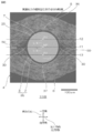
- FIG. 1 shows an image processing diagram of an SEM photograph of a vertical cross section of Example 1, which is a specific example of an embodiment of the inductor of the present invention.
- 2A to 2C are image processing diagrams of SEM photographs of the first flat cross section of the inductor shown in FIG. 1, FIG. 2A is a view of the first flat cross section, FIG. 2B is an enlarged view of FIG. 2A, and FIG. 2C. However, an enlarged view of FIG. 2B is shown.
- 3A to 3C are image processing diagrams of SEM photographs of the second flat cross section of the inductor shown in FIG. 1, where FIG. 3A is a view of the second flat cross section, FIG. 3B is an enlarged view of FIG. 3A, and FIG. 3C.
- FIG. 3B An enlarged view of FIG. 3B is shown.
- 4A to 4C are image processing diagrams of SEM photographs of the third planar cross section of the inductor shown in FIG. 1, FIG. 4A is a view of the third planar cross section, FIG. 4B is an enlarged view of FIG. 4A, and FIG. 4C.
- FIG. 4B an enlarged view of FIG. 4B is shown.
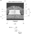
- 5A to 5C are process diagrams for explaining the manufacture of the inductor shown in FIG. 1, FIG. 5A is a process of preparing a first magnetic sheet and wiring, and FIG. 5B is a process of burying wiring in the first magnetic sheet.
- FIG. 5C show a step of sandwiching the wiring and the first magnetic sheet between the second magnetic sheet and the third magnetic sheet.
- FIG. 6 shows an image processing diagram of an SEM photograph of a vertical cross section of Example 2, which is a specific example of a modification of the inductor shown in FIG.
- FIG. 7 shows an image processing diagram of an SEM photograph of a vertical cross section of Example 3, which is a specific example of a modification of the inductor of the present invention.
- 8A to 8C are image processing diagrams of SEM photographs of the first flat cross section to the third flat cross section of the inductor shown in FIG. 7, FIG. 2A is a view of the first flat cross section, and FIG. 2B is a second flat cross section. A cross-sectional view, FIG.
- FIG. 9A to 9B are image processing diagrams of SEM photographs of the vertical cross section to the first flat cross section of Comparative Example 1, FIG. 9A shows a vertical cross section, and FIG. 9B shows a view of the first flat cross section.
- FIG. 10 shows an image processing diagram of an SEM photograph of the first flat cross section of Comparative Example 3.
- the inductor 1 has a shape extending in a plane direction orthogonal to the thickness direction (direction along the paper surface in FIGS. 2A to 4C).
- the inductor 1 has one surface 5 and the other surface 6 facing each other in the thickness direction.
- One surface 5 and the other surface 6 are substantially parallel to each other and each have a substantially flat shape.
- the inductor 1 includes a wiring 35 and a magnetic layer 4.
- a plurality of wirings 35 are provided in the inductor 1 at intervals in the plane direction when viewed in a vertical cross section 16 orthogonal to the direction along the wiring 35.
- the following description describes one wiring 35, but the same applies to the other wiring 35.
- the wiring 35 has a shape extending along one direction included in the surface direction of the inductor 1. Further, as shown in FIG. 1, the wiring 35 has a substantially circular shape when viewed in the vertical cross section 16.
- the wiring 35 includes a lead wire 2 and an insulating film 3.
- the lead wire 2 has a shape extending along the above-mentioned one direction. Further, as shown in FIG. 1, the lead wire 2 has a substantially circular shape when viewed in a vertical cross section 16 along a direction orthogonal to the flow direction (direction along the flow direction). As a result, the lead wire 2 has a lead wire circumferential surface 7 when viewed in the vertical cross section 16.
- the conducting wire 2 examples include metal conductors such as copper, silver, gold, aluminum, nickel, and alloys thereof, and copper is preferable.
- the conducting wire 2 may have a single-layer structure, or may have a multi-layer structure in which the surface of a core conductor (for example, copper) is plated (for example, nickel).
- the radius of the lead wire 2 is, for example, 25 ⁇ m or more, preferably 50 ⁇ m or more, and for example, 2000 ⁇ m or less, preferably 200 ⁇ m or less.
- the insulating film 3 protects the lead wire 2 from chemicals and water, and also prevents a short circuit between the lead wire 2 and the magnetic layer 4.
- the insulating film 3 is arranged on the peripheral surface of the conducting wire 2 when viewed in the vertical cross section 16. Specifically, the insulating film 3 covers the entire peripheral surface 7 (outer peripheral surface) of the conductive wire 2 when viewed in the vertical cross section 16. Further, the insulating film 3 has a substantially annular shape in cross section that shares the central axis (center) with the conducting wire 2. As a result, the insulating film 3 has an insulating circumferential surface 25 when viewed in the vertical cross section 16.
- Examples of the material of the insulating film 3 include insulating resins such as polyvinylformal, polyester, polyesterimide, polyamide (including nylon), polyimide, polyamideimide, and polyurethane. These may be used alone or in combination of two or more.
- insulating resins such as polyvinylformal, polyester, polyesterimide, polyamide (including nylon), polyimide, polyamideimide, and polyurethane. These may be used alone or in combination of two or more.
- the insulating film 3 may be composed of a single layer or may be composed of a plurality of layers.
- the thickness of the insulating film 3 is substantially uniform in the radial direction of the lead wire 2 at any position in the circumferential direction, for example, 1 ⁇ m or more, preferably 3 ⁇ m or more, and for example, 100 ⁇ m or less, preferably 100 ⁇ m or less. It is 50 ⁇ m or less.
- the ratio of the radius of the lead wire 2 to the thickness of the insulating film 3 is, for example, 1 or more, preferably 10 or more, and for example, 500 or less, preferably 100 or less.
- the radius of the wiring 35 is, for example, 25 ⁇ m or more, preferably 50 ⁇ m or more, and for example, 2000 ⁇ m or less, preferably 200 ⁇ m or less.
- the magnetic layer 4 improves the inductance of the inductor 1.
- Wiring 35 is embedded in the magnetic layer 4.
- the magnetic layer 4 is arranged on the peripheral surface of the insulating film 3 when viewed in the vertical cross section 16. Specifically, the magnetic layer 4 covers the entire surface of the insulating circumferential surface 25 (outer peripheral surface) of the insulating film 3.
- the magnetic layer 4 forms the outer shape of the inductor 1. Specifically, the magnetic layer 4 has a sheet shape and a rectangular shape extending in the plane direction. More specifically, the magnetic layer 4 has one surface and the other surface facing each other in the thickness direction, and one surface and the other surface of the magnetic layer 4 respectively have one surface 5 and the other surface 6 of the inductor 1. Form each of.
- the magnetic layer 4 contains anisotropic magnetic particles 8.
- the material of the magnetic layer 4 is a magnetic composition containing anisotropic magnetic particles 8 and a binder 9.
- the magnetic layer 4 is a cured product of a thermosetting resin composition (composition containing anisotropic magnetic particles 8 and a thermosetting component described later).
- Examples of the magnetic material constituting the anisotropic magnetic particles 8 include a soft magnetic material and a hard magnetic material.
- a soft magnetic material is preferably used from the viewpoint of inductance.
- the soft magnetic material examples include a single metal body containing one kind of metal element in a pure substance state, for example, one or more kinds of metal elements (first metal element) and one or more kinds of metal elements (second metal element).
- first metal element one or more kinds of metal elements
- second metal element one or more kinds of metal elements
- the single metal body examples include a single metal composed of only one kind of metal element (first metal element).
- the first metal element is appropriately selected from, for example, iron (Fe), cobalt (Co), nickel (Ni), and other metal elements that can be contained as the first metal element of the soft magnetic material. ..
- the single metal body includes, for example, a core containing only one kind of metal element and a surface layer containing an inorganic substance and / or an organic substance that modifies a part or all of the surface of the core, for example.
- examples thereof include an organic metal compound containing a first metal element and a form in which an inorganic metal compound is decomposed (thermal decomposition, etc.).
- thermal decomposition etc.
- iron powder obtained by thermally decomposing an organic iron compound (specifically, carbonyl iron) containing iron as the first metal element (sometimes referred to as carbonyl iron powder). And so on.
- the position of the layer containing the inorganic substance and / or the organic substance that modifies the portion containing only one kind of metal element is not limited to the above-mentioned surface.
- the organometallic compound or inorganic metal compound capable of obtaining a single metal body is not particularly limited, and a known or commonly used organometallic compound or inorganic metal compound capable of obtaining a soft magnetic single metal body is not particularly limited. Can be appropriately selected from.
- the alloy body is a eutectic of one or more kinds of metal elements (first metal element) and one or more kinds of metal elements (second metal element) and / or non-metal elements (carbon, nitrogen, silicon, phosphorus, etc.). It is not particularly limited as long as it is a body and can be used as an alloy body of a soft magnetic material.
- the first metal element is an essential element in the alloy body, and examples thereof include iron (Fe), cobalt (Co), and nickel (Ni). If the first metal element is Fe, the alloy body is an Fe-based alloy, and if the first metal element is Co, the alloy body is a Co-based alloy, and the first metal element is Ni. For example, the alloy body is a Ni-based alloy.
- the second metal element is an element (sub-component) secondarily contained in the alloy body, and is a metal element that is compatible (cofusable) with the first metal element.
- iron (Fe) the first. 1 When the metal element is other than Fe), Cobalt (Co) (when the first metal element is other than Co), Nickel (Ni) (when the first metal element is other than Ni), Chromium (Cr), Aluminum (Al), silicon (Si), copper (Cu), silver (Ag), manganese (Mn), calcium (Ca), barium (Ba), titanium (Ti), zirconium (Zr), ruthenium (Hf), vanadium (V), Niob (Nb), Tantal (Ta), Molybdenum (Mo), Tungsten (W), Ruthenium (Ru), Rodium (Rh), Zinc (Zn), Gallium (Ga), Indium (In), Germanium Examples thereof include (Ge), tin (Sn), lead (Pb), scandium (Sc), rut
- the non-metal element is an element (sub-component) secondarily contained in the alloy body, and is a non-metal element that is compatible (combined) with the first metal element.
- boron (B) and carbon examples thereof include (C), nitrogen (N), silicon (Si), phosphorus (P) and sulfur (S). These can be used alone or in combination of two or more.
- Fe-based alloys examples include magnetic stainless steel (Fe-Cr-Al-Si alloy) (including electromagnetic stainless steel), sentust (Fe-Si-Al alloy) (including super sentust), and permalloy (including supersendust).
- magnetic stainless steel Fe-Cr-Al-Si alloy
- sentust Fe-Si-Al alloy
- permalloy including supersendust
- Fe-Ni alloy Fe-Ni alloy
- Fe-Ni-Mo alloy Fe-Ni-Mo-Cu alloy
- Fe-Ni-Co alloy Fe-Cr alloy
- Fe-Cr-Al alloy Fe-Ni-Cr alloy
- Fe- Ni—Cr—Si alloy silicon copper (Fe—Cu—Si alloy)
- Fe—Si alloy Fe—Si—B (—Cu—Nb) alloy
- Fe—B—Si—Cr alloy Fe—Si—Cr -Ni alloy
- Fe-Si-Cr alloy Fe-Si-Al-Ni-Cr alloy
- Fe-Ni-Si-Co alloy Fe-N alloy, Fe-C alloy, Fe-B alloy, Fe-P alloy
- Ferrites stainless ferrites, Mn-Mg-based ferrites, Mn-Zn-based ferrites, Ni-Zn-based ferrites, Ni-Zn-Cu-based ferrites, Cu-Zn-based ferrites, Cu-Mg-Zn-based
- Co-based alloys examples include Co-Ta-Zr and cobalt (Co) -based amorphous alloys.
- Ni-based alloys which are examples of alloys, include Ni—Cr alloys.
- an alloy body is preferable, an Fe-based alloy is more preferable, and Sendust (Fe—Si—Al alloy) is more preferable, from the viewpoint of magnetic properties.
- the soft magnetic material preferably a single metal body, more preferably a single metal body containing an iron element in a pure substance state, still more preferably iron alone or iron powder (carbonyl iron powder). Can be mentioned.
- the shape of the anisotropic magnetic particles 8 examples include a flat shape (plate shape) and a needle shape from the viewpoint of anisotropy (or orientation), and are preferably compared to the plane direction (two-dimensional). From the viewpoint of good magnetic permeability, a flat shape can be mentioned.
- the magnetic layer 4 may further contain non-anisotropic magnetic particles in addition to the anisotropic magnetic particles 8.
- the non-anisotropic magnetic particles may have a shape such as a spherical shape, a granular shape, a lump shape, or a pellet shape.
- the average particle size of the non-anisotropic magnetic particles is, for example, 0.1 ⁇ m or more, preferably 0.5 ⁇ m or more, and for example, 200 ⁇ m or less, preferably 150 ⁇ m or less.
- the flatness (flatness) of the flat anisotropic magnetic particles 8 is, for example, 8 or more, preferably 15 or more, and for example, 500 or less, preferably 450 or less.
- the flatness is calculated as, for example, an aspect ratio obtained by dividing the average particle diameter (average length) (described later) of the anisotropic magnetic particles 8 by the average thickness of the anisotropic magnetic particles 8.
- the average particle diameter (average length) of the anisotropic magnetic particles 8 is, for example, 3.5 ⁇ m or more, preferably 10 ⁇ m or more, and for example, 200 ⁇ m or less, preferably 150 ⁇ m or less. If the anisotropic magnetic particles 8 are flat, the average thickness thereof is, for example, 0.1 ⁇ m or more, preferably 0.2 ⁇ m or more, and for example, 3.0 ⁇ m or less, preferably 2.5 ⁇ m. It is as follows.
- the proportion of the anisotropic magnetic particles 8 in the magnetic layer 4 is 40% by volume or more, preferably 45% by volume or more, more preferably 50% by volume or more, still more preferably 55% by volume or more, and particularly preferably 60. It is more than% by volume. If the ratio of the anisotropic magnetic particles 8 in the magnetic layer 4 does not meet the above lower limit, the inductor 1 cannot obtain an excellent inductance.
- the proportion of the anisotropic magnetic particles 8 in the magnetic layer 4 is, for example, 95% by volume or less, preferably 90% by volume or less.
- the proportion of the anisotropic magnetic particles 8 is equal to or less than the above upper limit, the inductor 1 has excellent mechanical strength.
- the binder 9 is a matrix in which the anisotropic magnetic particles 8 are dispersed in the magnetic layer 3. Further, the binder 9 is dispersed in the magnetic layer 3 in a predetermined direction.
- examples of the binder 9 include a thermoplastic component such as an acrylic resin, and a thermosetting component such as an epoxy resin composition.
- Acrylic resins include, for example, carboxyl group-containing acrylic acid ester copolymers.
- the epoxy resin composition contains, for example, an epoxy resin (cresol novolac type epoxy resin or the like) as a main agent, a curing agent for epoxy resin (phenol resin or the like), and a curing accelerator for epoxy resin (imidazole compound or the like).
- the binder 9 contains a cured product of a thermosetting component.
- the proportion of the binder 9 in the magnetic composition is the balance of the anisotropic magnetic particles 8.
- the anisotropic magnetic particles 8 covering the insulating circumferential surface 25 of the insulating film 3 are oriented, for example, along the circumferential direction of the conducting wire 2. Further, if the anisotropic magnetic particles 8 are flat, the anisotropic magnetic particles 8 covering the insulating circumferential surface 25 are oriented in the circumferential direction when the magnetic layer 4 is viewed in the vertical cross section 16.
- the first flat cross section 11, the second flat cross section 12, and the third flat cross section 13 are defined as follows.
- the first flat cross section 11 is a central flat cross section that passes through the midpoint MP of the line segment L connecting the one end edge 36 and the other end edge 37 in the thickness direction of the lead wire 2.
- the first flat cross section 11 is along the plane direction of the inductor 1. Specifically, the first flat cross section 11 is substantially parallel to at least the other surface 6 in the thickness direction of the inductor 1.
- the second flat cross section 12 is a flat cross section that passes through the first point P1 located at a position where the length (1/4 L) of 1/4 of the line segment L is advanced from the midpoint MP to one side in the thickness direction.
- the second flat cross section 12 is along the plane direction of the inductor 1. Specifically, the second flat cross section 12 is parallel to the first flat cross section 11.
- the third flat cross section 13 is the other flat cross section that passes through the second point P2 at a position where the length (1 / 4L) is advanced from the midpoint MP to the other side in the thickness direction.
- the third flat cross section 33 is along the plane direction of the inductor 1. Specifically, the third flat cross section 33 is parallel to the first flat cross section 11.
- the neighboring region 10 and the outer region 20 are arranged in this order in the first direction (corresponding to the left-right direction of FIGS. .
- the insulating film 3 is arranged in order from the outer edge 30 toward the outside in the first direction, and there is no gap between the neighboring region 10 and the outer region 20 and they are continuous with each other.
- the vicinity region 10 is a region within 50 ⁇ m outward from the outer edge 30 of the insulating film 3 in the first direction in the first direction, and is a band-shaped region along the flow direction. Further, the vicinity region 10 is a portion that has a stronger influence on the inductance of the inductor 1 than the outer region 20 described below.
- the outer region 20 has a first outer region 17, a second outer region 18, and a third outer region 19.
- the first outer region 17, the second outer region 18, and the third outer region 19 are arranged in parallel in this order toward the outside in the first direction.
- the first outer region 17 is adjacent to the outer side of the neighboring region 10 in the first direction. Specifically, the first outer region 17 is a region within 75 ⁇ m in excess of 50 ⁇ m from the outer edge 30 in the first direction of the insulating film 3 in the first direction, and is a band-shaped region along the flow direction. .. That is, the first outer region 17 is a region within 25 ⁇ m from the outer edge of the neighboring region 10 in the first direction.
- the second outer region 18 is adjacent to the outer side of the first outer region 17 in the first direction.
- the second outer region 18 is a region that is more than 75 ⁇ m and 95 ⁇ m or less outward from the outer edge 30 of the insulating film 3 in the first direction in the first direction, and is a band-shaped region along the flow direction. .. That is, the second outer region 18 is a region within 20 ⁇ m from the outer edge of the first outer region 17 in the first direction.
- the third outer region 19 is adjacent to the outer side of the second outer region 18 in the first direction.
- the third outer region 19 is a region that is more than 95 ⁇ m and 105 ⁇ m or less outward from the outer edge 30 of the insulating film 3 in the first direction in the first direction, and is a band-shaped region along the flow direction. .. That is, the third outer region 19 is a region within 10 ⁇ m from the outer edge of the second outer region 18 in the first direction.
- the anisotropic magnetic particles 8 are electrically in the vicinity region 10 at least.
- An orientation region oriented in a substantially linear shape along the flow direction is observed.
- the anisotropic magnetic particles 8 are oriented in the flow direction.
- the case where the above angle exceeds 15 degrees is defined as "the anisotropic magnetic particles 8 are not oriented in the flow direction”.
- the orientation region is the sum of the number of anisotropic magnetic particles 8 oriented in the flow direction, the number of anisotropic magnetic particles 8 oriented in the flow direction, and the number of anisotropic magnetic particles 8 not oriented in the flow direction. It is a region in which the ratio with respect to 50% is more than 50%, preferably 60% or more, more preferably 70% or more, still more preferably 75% or more, and particularly preferably 80% or more.
- the orientation region is observed in the vicinity region 10 and the first outer region 17 when viewed in any of the first flat cross section 11, the second flat cross section 12, and the third flat cross section 13.
- first flat cross section 11 or second flat cross section 12 of the first flat cross section 11, the second flat cross section 12, and the third flat cross section 13, and two more. Orientation regions are observed in the neighborhood region 10, the first outer region 17, and the second outer region 18 when viewed in planographic sections (eg, first flat section 11 and second flat section 12).
- the orientation region when viewed in one flat section (specifically, the first flat cross section 11) of the first flat cross section 11, the second flat cross section 12, and the third flat cross section 13, the orientation region is It is observed in the vicinity region 10, the first outer region 17, the second outer region 18, and the third outer region 19.
- the orientation regions are the neighborhood region 10 and the first outer region 17 when viewed in the first flat cross section 11, as referred to the first column of Example 2 in Table 2.
- the second outer region 18 and the third outer region 19 are observed.
- the orientation region is observed in the neighboring region 10, the first outer region 17 and the second outer region 18, while the third outer region 19 is observed.
- the orientation region is observed in the neighborhood region 10 and the first outer region 17, while the second outer region 18 and the third outer region 19 are observed.
- the orientation region is observed in both the near region 10 and the outer region 20.
- the anisotropic magnetic particles 8 are oriented along the flow direction, and the vertical cross section 16 is formed.
- the lead wire 2 is oriented along the circumferential direction.
- the aspect ratio of the anisotropic magnetic particle 8 itself is 100
- the aspect ratio observed in the first flat cross section 11 specifically, the aspect ratio of the anisotropic magnetic particle 8 in the above-mentioned cross-sectional view (vertical direction).
- the length l / lateral length w) is, for example, 50 or more, preferably 75 or more
- the anisotropic magnetic particle 8 has a flow direction and a flow direction. It can be defined as being oriented along the circumferential direction of the lead wire 2.
- the anisotropic magnetic particles 8 are oriented in both the flow direction and the circumferential direction, a magnetic path that surrounds the conducting wire 2 and follows the flow of electricity is formed in the magnetic layer 4, whereby the inductor 1 of the inductor 1 is formed.
- the inductance can be improved.
- the orientation region when viewed in the first flat cross section 11, the second flat cross section 12, and the third flat cross section 13, the orientation region may be observed in the outer region 20 and also in the portion outside the third outer region 19. Or, it does not have to be observed.
- the intersection (top) 50 is formed by two types of anisotropic magnetic particles 8 having different orientation directions.
- the intersection 50 is located on the other side in the thickness direction from the third flat cross section 13.
- the intersection 50 passes through the other end edge 37 of the lead wire 2 and is located on one side in the thickness direction of the fifth cross section (not shown) parallel to the third flat cross section 13. That is, the intersection 50 is located between the third cross section 13 and the fifth cross section (not shown).
- the thickness of the magnetic layer 4 is, for example, twice or more, preferably three times or more, and for example, 20 times or less the radius of the lead wire 2. Specifically, the thickness of the magnetic layer 4 is, for example, 100 ⁇ m or more, preferably 200 ⁇ m or more, and for example, 2000 ⁇ m or less, preferably 1000 ⁇ m or less. The thickness of the magnetic layer 4 is the distance between one surface 5 and the other surface 6 of the magnetic layer 4.
- the thickness of the inductor 1 is the same as the thickness of the magnetic layer 4 described above.
- the wiring 35 is first prepared, the magnetic sheet 24 is prepared, and then, as shown in FIG. 5B, the wiring 35 is connected by the magnetic sheet 24.
- the magnetic layer 4 is formed by burying them together.
- the magnetic sheet 24 may be one sheet, or may include a plurality of sheets. Specifically, the magnetic sheet 24 includes at least the first magnetic sheet 21 (FIG. 5A), preferably the first magnetic sheet 21, the second magnetic sheet 22 (FIG. 5B), and the third magnetic sheet 23 (FIG. 5B). 5B) is included separately.
- Each material of the first magnetic sheet 21, the second magnetic sheet 22, and the third magnetic sheet 23 contains the above-mentioned anisotropic magnetic particles 8 and the binder 9, and has a sheet shape extending in the plane direction.
- Each of the first magnetic sheet 21, the second magnetic sheet 22, and the third magnetic sheet 23 is preferably prepared as a B stage sheet.
- Each of the first magnetic sheet 21, the second magnetic sheet 22, and the third magnetic sheet 23 may be a single layer, or may be a multilayer (specifically, the inner sheet and the lead wire 2 with respect to the inner sheet. It may be composed of an outer sheet located on the opposite side of the.
- Examples of the first magnetic sheet 21, the second magnetic sheet 22, and the third magnetic sheet 23 include soft magnetic thermosetting adhesive films described in JP-A-2014-165363, JP-A-2015-92544, and the like. ..
- the wiring 35 is embedded by the first magnetic sheet 21 shown by the solid line (preferably, the wiring 35 is heat-pressed). As a result, the intersection 50 is formed on the first magnetic sheet 21.
- the second magnetic sheet 22 and the third magnetic sheet 23 are sandwiched between the wiring 35 and the first magnetic sheet 21 in the thickness direction to form the first magnetic sheet.
- the sheet 21 is arranged on one side and the other side in the thickness direction (preferably heat-pressed). As a result, the magnetic layer 4 having one surface 5 and the other surface 6 is formed.
- the magnetic layer 4 is in the B stage, it is converted into the C stage.
- FIG. 5C shows the boundary between the first magnetic sheet 21 and the second magnetic sheet 22 and the boundary between the first magnetic sheet 21 and the third magnetic sheet 23, but as can be seen from the SEM photograph of FIG. They may be ambiguous.
- the region 10 an orientation region in which the anisotropic magnetic particles 8 are oriented in the flow direction is observed. Therefore, in the vicinity region 10, a magnetic path along the flow direction is formed.
- the conducting wire 2 has the guiding wire circumferential surface 7 when viewed in a vertical cross section, the anisotropic magnetic particles 8 are oriented in the flow direction in the magnetic layer 4 facing the guiding wire circumferential surface 7. easy.
- the magnetic layer 4 contains 40% by volume or more of the anisotropic magnetic particles 8.
- this inductor 1 has excellent inductance.
- the inductor 1 of this embodiment when the magnetic layer 4 is viewed in each of the first flat cross section 11, the second flat cross section 12, and the third flat cross section 13, the orientation region is located in the vicinity region 10. As observed, the inductor 1 is even better due to the inductance.
- the plane direction of the anisotropic magnetic particles 8 is oriented in the circumferential direction of the lead wire 2. Therefore, a magnetic path surrounding the lead wire 2 is formed. As a result, the inductance is even better.
- the orientation region is observed in any of the neighboring regions 10 of the first flat cross section 11, the second flat cross section 12 and the third flat cross section 13. To.
- the cross section in which the orientation region is observed is not limited to all (three) of the above three, and may be two.
- the alignment region is observed in the neighborhood region 10 (furthermore, the first outer region 17 and the second outer region 18), while the orientation region is the neighborhood region when viewed in the first flat cross section 11. Not observed at 10.
- the intersection 50 is located on, for example, the first flat cross section 11.
- the orientation region is observed in the vicinity region 10 in the second flat cross section 12 and the third flat cross section 13.
- two of the three flat cross sections are not limited to the above-mentioned second flat cross section 12 and third flat cross section 13, but the first flat cross section 11 and the second flat cross section 12 (FIGS. 7 to 8C described later). (See), or it may be either the first flat cross section 11 or the third flat cross section 13.
- the orientation region is the neighborhood region 10 when viewed in the third flat cross section 13. Not observed in. Further, when the alignment region is observed in the vicinity region 10 when viewed in the first flat cross section 11 and the third plane cross section 13, the orientation region is the neighborhood region 10 when viewed in the second flat cross section 12. Not observed in.
- the orientation region is located in the vicinity region 10.
- the inductor 1 of the embodiment shown in FIGS. 1 to 4C is more excellent in inductance than the modified example inductor 1 shown in FIGS. 6 to 7C.
- the wiring 35 and the lead wire 2 have a substantially circular shape when viewed in the vertical cross section 16, but, for example, as shown in FIG. 7, they have a substantially rectangular shape. There may be.
- This inductor 1 includes a conductor pattern 38 as an example of a conducting wire, an insulating film 3, and a magnetic layer 4.
- the inductor 1 is a modification in which the orientation region is observed in the vicinity region 10 in the first flat cross section 11 and the second flat cross section 12, which are two of the three flat cross sections.
- the conductor pattern 38 includes one surface 39 and the other surface 40 facing in the thickness direction and two connecting surfaces 41 connecting both ends of the one surface 39 and the other surface 40 in the first direction when viewed in the vertical cross section 16. Is provided integrally.
- Each of the one surface 39 and the other surface 40 is a flat surface and is parallel to each other.
- the insulating film 3 may cover the entire outer peripheral surface of the lead wire 2.
- the conductor pattern 38 has two corners 42 formed by one surface 39 and a connecting surface 41, and each of the two corners 42 constitutes a curved portion (curved surface).
- the radius of curvature of the curved surface of the corner 42 is, for example, 5 ⁇ m or more and 30 ⁇ m or less.
- the thickness of the conductor pattern 38 is the distance between the one surface 39 and the other surface 40.
- the width of the conductor pattern 38 is the average distance between the two connecting surfaces 41, and is, for example, 20 ⁇ m or more and 1000 ⁇ m or less.
- the insulating film 3 is arranged on one surface 39, the other surface 40, and the connecting surface 41 of the conductor pattern 38.
- the magnetic layer 4 has a first magnetic layer 45 and a second magnetic layer 46.
- the first magnetic layer 45 has a substantially plate shape extending in the plane direction.
- the material of the first magnetic layer 45 is the above-mentioned magnetic composition.
- the anisotropic magnetic particles 8 are oriented in the flow direction and the plane direction.
- the second magnetic layer 46 has a sheet shape extending in the plane direction. One surface of the second magnetic layer 46 in the thickness direction is exposed toward one side in the thickness direction, and the other surface of the second magnetic layer 46 covers one surface 39 of the conductor pattern 38 and the connecting surface 41, and is a conductor. It is in contact with one surface of the first magnetic layer 45 exposed from the pattern 38.
- the anisotropic magnetic particles 8 facing the one surface 39 are oriented in the plane direction and the flow direction, and the anisotropic magnetic particles 8 facing the connecting surface 41 have a thickness as described later.
- the anisotropic magnetic particles 8 that are oriented along the direction and the flow direction and that face the corner portion 42 are oriented along the circumferential direction and the flow direction centered on the corner portion 42.
- the corner portion 42 of the conductor pattern 38 does not have to have a curved portion, that is, a curved surface.
- the corner 42 is a bent portion that bends at, for example, 45 degrees or more, 60 degrees or more, 75 degrees or more, and for example, 135 degrees or less, 120 degrees or less, 105 degrees or less (more specifically, 90 degrees). There may be.
- the inductor 1 includes a plurality of wirings 35, but for example, one wiring 35 can also be provided.
- the definition of the vicinity region 10 is expressed using the absolute distance from the outer edge 30 in the first direction, but it can also be expressed using the relative distance.
- the anisotropic magnetic particle 8 is flat. If this is the case, it can be defined as a region within 0.08 with respect to the average thickness of the anisotropic magnetic particles 8 from the outer edge 30 in the first direction to the outside in the first direction. That is, the ratio of the above-mentioned distance to the average thickness of the anisotropic magnetic particles 8 can be 0.08.
- the first outer region 17 can be defined as a region exceeding 0.08 and within 0.13 from the outer edge 30 in the first direction to the outside in the first direction, and is the second outer region.
- the region 18 can be defined as a region exceeding 0.13 and within 0.175 from the outer edge 30 in the first direction, and the third outer region 19 is outside the outer edge 30 in the first direction in the first direction. Can be defined as a region greater than 0.175 and within 0.225.
- the proportion of the anisotropic magnetic particles 8 in the magnetic layer 4 may be uniform in the magnetic layer 4, and may be increased or decreased as the distance from each wiring 2 increases.
- the proportion of the anisotropic magnetic particles 8 in the magnetic layer 4 increases as the distance from the wiring 35 increases, for example, as shown in FIG. 5B, the anisotropic magnetic particles in the second magnetic sheet 22.
- the abundance ratio of 8 and the abundance ratio of the anisotropic magnetic particles 8 on the third magnetic sheet 23 are set higher than the abundance ratio of the anisotropic magnetic particles 8 on the first magnetic sheet 21.
- Examples and comparative examples are shown below, and the present invention will be described in more detail.
- the present invention is not limited to Examples and Comparative Examples.
- specific numerical values such as the compounding ratio (content ratio), physical property values, and parameters used in the following description are the compounding ratios corresponding to those described in the above-mentioned "Form for carrying out the invention".
- Content ratio can be replaced with the upper limit (numerical value defined as “less than or equal to” or “less than”) or lower limit (numerical value defined as "greater than or equal to” or “excess”). it can.
- Example 1 Example drawn in FIGS. 1 to 4C ⁇ Inductor based on one embodiment> The inductor 1 was manufactured based on one embodiment. Specifically, a wiring 35 including a lead wire 2 made of copper having a radius of 100 ⁇ m and an insulating film 3 having a thickness of 10 ⁇ m was prepared. Separately, the first magnetic sheet 21 was prepared as a B stage sheet. The layer structure and formulation of the first magnetic sheet 21 are shown in Table 1.
- the first magnetic sheet 21 was then attached (heat pressed) to the wiring 35.
- the second magnetic sheet 22 and the third magnetic sheet 23 were prepared as B stage sheets.
- the layer structure and formulation of the second magnetic sheet 22 and the third magnetic sheet 23 are shown in Table 1.
- the wiring 35 and the first magnetic sheet 21 were sandwiched between the second magnetic sheet 22 and the third magnetic sheet 23, and they were attached (heat pressed).
- thermosetting components in the first magnetic sheet 21, the second magnetic sheet 22, and the third magnetic sheet 23 were C-staged.
- the wiring 35 is embedded by the magnetic layer 4 composed of the first magnetic sheet 21, the second magnetic sheet 22, and the third magnetic sheet 23 of the C stage, and as shown in FIG. 1, the wiring 35 and the magnetic layer 4 An inductor 1 comprising the above was manufactured.
- the obtained inductor 1 was subjected to SEM observation of each of the vertical cross section 16, the first flat cross section 11, the second flat cross section 12, and the third flat cross section 13, and an attempt was made to observe the orientation region.
- the image processing diagrams are shown in FIGS. 1 to 4C, and the observation results of the orientation region are shown in Table 2.
- Example 2 Example drawn in FIG. 6 ⁇ Example of manufacturing an inductor based on a modified example of one embodiment> The inductor 1 shown in FIG. 6 was obtained in the same manner as in the first embodiment except that the wiring 35 was sandwiched between the second magnetic sheet 22 and the third magnetic sheet 23 without using the first magnetic sheet 21. SEM observations of the plan surface 11, the second flat section 12, and the third flat section 13 were carried out.
- Table 2 shows the observation results of the orientation region.
- Example 3 Example drawn in FIGS. 7 to 8C ⁇ Example of manufacturing an inductor based on a modified example of one embodiment>
- the cross-sectional area (regular cross-sectional area) in the vertical cross section 16 is the same as that in the first embodiment, but the inductor 1 is obtained in the same manner as in the first embodiment except that the substantially rectangular conducting wire 2 is used. SEM observations of the cross section 11, the second flat cross section 12, and the third flat cross section 13 were carried out.
- the lead wire 2 was covered with the B stage sheet via the insulating film 3.
- Table 2 shows the observation results of the orientation region.
- Comparative Example 1 Example drawn in FIGS. 9A to 9B Inductor 1 in the same manner as in Example 2 in which the second magnetic sheet 22 and the third magnetic sheet 23 at the time of bonding to the wiring 35 are changed to a cured body of the C stage.
- the SEM observations of the first flat cross section 11, the second flat cross section 12, and the third flat cross section 13 were carried out.
- Table 3 shows the observation results of the orientation region.
- Comparative Example 2 An inductor 1 was obtained in the same manner as in Example 3 in which the second magnetic sheet 22 and the third magnetic sheet 23 at the time of bonding were changed to a cured body of the C stage, and the first flat cross section 11 and the second flat cross section 12 were obtained. And each SEM observation of the third plane cross section 13 was carried out.
- Table 3 shows the observation results of the orientation region.
- Comparative Example 3 Example drawn in FIG. 10
- the inductor 1 is the same as in Example 11 except that spherical magnetic particles (average particle diameter 20 ⁇ m, Fe—Si—Al alloy) are used instead of the anisotropic magnetic particles 8.
- spherical magnetic particles average particle diameter 20 ⁇ m, Fe—Si—Al alloy
- Table 3 shows the observation results of the orientation region.
- the inductor is mounted on, for example, an electronic device.
Abstract
An inductor 1 is provided with a wire 35 and a sheet-shaped magnetic layer 4 in which the wire 35 is embedded. The wire 35 is provided with a conductor 2 and an insulating film 3 positioned on the circumferential surface of the conductor 2. The magnetic layer 4 contains at least 40 vol% of anisotropic magnetic particles 8. When viewed in at least two planar cross-sections among a first planar cross-section 11, a second planar cross-section 12 and a third planar cross-section 13 along the surface direction of the magnetic layer 4, in a first direction that is orthogonal to a flow direction and a thickness direction, an alignment area in which the anisotropic magnetic particles 8 are aligned in the flow direction is observed in a proximity area 10 within 50 μm to the outside from the outer edge 30 of the insulating film 3, in the first direction. The first planar cross-section 11 passes through a midpoint MP of a line segment L of the conductor 2. The second planar cross-section 12 passes through a first point P1 which is a position where a length 1/4 L extends to one side in the thickness direction from the midpoint MP. The third planar cross-section 13 passes through a second point P2 which is a position where the length 1/4 L extends to the other side in the thickness direction from the midpoint MP.
Description
本発明は、インダクタに関する。
The present invention relates to an inductor.
従来、インダクタは、電子機器などに搭載されて、電圧変換部材などの受動素子として用いられることが知られている。
Conventionally, it is known that inductors are mounted on electronic devices and used as passive elements such as voltage conversion members.
例えば、磁性体材料からなる直方体状のチップ本体部と、そのチップ本体部の内部に埋設された内部導体とを備えるインダクタが提案されている(例えば、下記特許文献1参照。)。
For example, an inductor having a rectangular parallelepiped chip body made of a magnetic material and an internal conductor embedded inside the chip body has been proposed (see, for example, Patent Document 1 below).
近年、インダクタには、高いレベルのインダクタンスが要求される。しかし、特許文献1のインダクタは、上記した要求を満足することができないという不具合がある。
In recent years, inductors are required to have a high level of inductance. However, the inductor of Patent Document 1 has a problem that it cannot satisfy the above-mentioned requirements.
本発明は、インダクタンスに優れるインダクタを提供する。
The present invention provides an inductor having excellent inductance.
本発明(1)は、導線、および、前記導線の周面に配置される絶縁膜を備える配線と、前記配線を埋設する磁性層とを備えるインダクタであって、前記磁性層は、異方性磁性粒子を40体積%以上含み、前記磁性層の厚み方向に直交する面方向に沿う第1平断面、第2平断面および第3平断面のうち、少なくとも2つの前記平断面のそれぞれで視たときに、前記流れ方向および厚み方向に直交する第1方向において、前記絶縁膜の外端縁から外側に50μm以内の近傍領域において、前記異方性磁性粒子が前記流れ方向に配向する配向領域が観察される、インダクタを含む。
The present invention (1) is an inductor including a lead wire, a wire having an insulating film arranged on the peripheral surface of the lead wire, and a magnetic layer in which the wire is embedded, and the magnetic layer is anisotropic. Each of at least two of the first flat cross section, the second flat cross section, and the third flat cross section, which contains 40% by volume or more of magnetic particles and is along the plane direction orthogonal to the thickness direction of the magnetic layer, is viewed. Occasionally, in the first direction orthogonal to the flow direction and the thickness direction, an orientation region in which the anisotropic magnetic particles are oriented in the flow direction is formed in a region within 50 μm outward from the outer edge of the insulating film. Observed, including inductor.
前記第1平断面:前記導線の前記厚み方向一端縁および他端縁間を結ぶ線分Lの中点を通過する。
The first flat cross section: passes through the midpoint of the line segment L connecting the one end edge and the other end edge of the lead wire in the thickness direction.
前記第2平断面:前記線分Lの1/4の長さ(1/4L)を前記中点から前記厚み方向一方側に進んだ位置にある第1点を通過する。
The second flat cross section: Passes a first point located at a position where the length (1/4 L) of 1/4 of the line segment L is advanced from the midpoint to one side in the thickness direction.
前記第3平断面:前記長さ(1/4L)を前記中点から前記厚み方向他方側に進んだ位置にある第2点を通過する。
The third flat cross section: Passes the second point at a position where the length (1 / 4L) is advanced from the midpoint to the other side in the thickness direction.
このインダクタでは、第1平断面、第2平断面および第3平断面のうち、少なくとも2つの平断面のそれぞれで視たときに、近傍領域において、異方性磁性粒子が流れ方向に配向する配向領域が観察される。そのため、インダクタのインダクタンスに強い影響を及ぼす近傍領域では、流れ方向に沿う磁路が形成される。
In this inductor, when viewed in at least two flat cross sections of the first flat cross section, the second flat cross section, and the third flat cross section, the anisotropic magnetic particles are oriented in the flow direction in the vicinity region. The area is observed. Therefore, a magnetic path along the flow direction is formed in the near region that strongly affects the inductance of the inductor.
また、磁性層は、異方性磁性粒子を40体積%以上と高い割合で含む。
Further, the magnetic layer contains anisotropic magnetic particles in a high proportion of 40% by volume or more.
従って、このインダクタは、インダクタンスに優れる。
Therefore, this inductor has excellent inductance.
本発明(2)は、前記第1平断面、前記第2平断面および前記第3平断面のそれぞれで前記磁性層を視たときに、前記近傍領域において、前記配向領域が観察される、(1)に記載のインダクタを含む。
In the present invention (2), when the magnetic layer is viewed in each of the first flat cross section, the second flat cross section, and the third flat cross section, the orientation region is observed in the vicinity region (2). 1) The inductor according to 1) is included.
このインダクタ1では、第1平断面、第2平断面および第3平断面の全てにおいて、近傍領域で、配向領域が観察されるので、インダクタは、インダクタンスにより一層優れる。
In this inductor 1, the orientation region is observed in the vicinity region in all of the first flat cross section, the second flat cross section, and the third flat cross section, so that the inductor is more excellent in inductance.
本発明(3)は、前記導線は、前記配線に沿う方向に直交する断面で視たときに、略円形状を有し、前記異方性磁性粒子が、略板状を有し、前記配向領域では、前記異方性磁性粒子の面方向が、前記導線の周方向に沿っている、(1)または(2)に記載のインダクタを含む。
In the present invention (3), the conducting wire has a substantially circular shape when viewed in a cross section orthogonal to the direction along the wiring, and the anisotropic magnetic particles have a substantially plate shape, and the orientation thereof. The region includes the inductor according to (1) or (2), wherein the plane direction of the anisotropic magnetic particles is along the circumferential direction of the lead wire.
このインダクタの配向領域では、異方性磁性粒子の面方向が、導線の周方向に配向される。そのため、導線を囲む磁路が形成される。その結果、インダクタンスにより一層優れる。
In the orientation region of this inductor, the plane direction of the anisotropic magnetic particles is oriented in the circumferential direction of the conducting wire. Therefore, a magnetic path surrounding the conducting wire is formed. As a result, the inductance is even better.
本発明のインダクタは、インダクタンスに優れる。
The inductor of the present invention has excellent inductance.
本発明のインダクタの一実施形態を、図1A~図4Cで示すSEM写真に基づいて、説明する。
An embodiment of the inductor of the present invention will be described with reference to the SEM photographs shown in FIGS. 1A to 4C.
図1に示すように、インダクタ1は、厚み方向に直交する面方向(図2A~図4Cにおける紙面に沿う方向)に延びる形状を有する。インダクタ1は、厚み方向に対向する一方面5および他方面6を有する。一方面5および他方面6は、互いに実質的に平行し、それぞれ、略平坦形状を有する。
As shown in FIG. 1, the inductor 1 has a shape extending in a plane direction orthogonal to the thickness direction (direction along the paper surface in FIGS. 2A to 4C). The inductor 1 has one surface 5 and the other surface 6 facing each other in the thickness direction. One surface 5 and the other surface 6 are substantially parallel to each other and each have a substantially flat shape.
インダクタ1は、配線35と、磁性層4とを備える。
The inductor 1 includes a wiring 35 and a magnetic layer 4.
配線35は、配線35に沿う方向に直交する縦断面16で視たときに、インダクタ1において面方向に互いに間隔を隔てて複数設けられている。なお、以下の説明は、一の配線35について説明するが、他の配線35についても同様である。
A plurality of wirings 35 are provided in the inductor 1 at intervals in the plane direction when viewed in a vertical cross section 16 orthogonal to the direction along the wiring 35. The following description describes one wiring 35, but the same applies to the other wiring 35.
配線35は、図2Aに示すように、インダクタ1の面方向に含まれる一方向に沿って延びる形状を有する。また、図1に示すように、配線35は、縦断面16で視たときに、略円形状を有する。
As shown in FIG. 2A, the wiring 35 has a shape extending along one direction included in the surface direction of the inductor 1. Further, as shown in FIG. 1, the wiring 35 has a substantially circular shape when viewed in the vertical cross section 16.
なお、「縦断面16で視たとき」とは、縦断面16に沿う切断面を作製し、これをSEM観察したときを含む。後述する縦断面16、第1平断面11、第2平断面12および第3平断面13で視たときも、上記と同様である。
Note that "when viewed in the vertical cross section 16" includes the case where a cut surface along the vertical cross section 16 is prepared and observed by SEM. The same applies to the vertical cross section 16, the first flat cross section 11, the second flat cross section 12, and the third flat cross section 13, which will be described later.
配線35は、導線2および絶縁膜3を備える。
The wiring 35 includes a lead wire 2 and an insulating film 3.
導線2は、上記した一方向に沿って延びる形状を有する。また、図1に示すように、導線2は、流れ方向(沿う方向)に直交する方向に沿う縦断面16で視たときに、略円形状を有する。これにより、導線2は、縦断面16で視たときに、導線円周面7を有する。
The lead wire 2 has a shape extending along the above-mentioned one direction. Further, as shown in FIG. 1, the lead wire 2 has a substantially circular shape when viewed in a vertical cross section 16 along a direction orthogonal to the flow direction (direction along the flow direction). As a result, the lead wire 2 has a lead wire circumferential surface 7 when viewed in the vertical cross section 16.
導線2の材料としては、例えば、銅、銀、金、アルミニウム、ニッケル、これらの合金などの金属導体が挙げられ、好ましくは、銅が挙げられる。導線2は、単層構造であってもよく、コア導体(例えば、銅)の表面にめっき(例えば、ニッケル)などがされた複層構造であってもよい。
Examples of the material of the conducting wire 2 include metal conductors such as copper, silver, gold, aluminum, nickel, and alloys thereof, and copper is preferable. The conducting wire 2 may have a single-layer structure, or may have a multi-layer structure in which the surface of a core conductor (for example, copper) is plated (for example, nickel).
導線2の半径は、例えば、25μm以上、好ましくは、50μm以上であり、また、例えば、2000μm以下、好ましくは、200μm以下である。
The radius of the lead wire 2 is, for example, 25 μm or more, preferably 50 μm or more, and for example, 2000 μm or less, preferably 200 μm or less.
絶縁膜3は、導線2を薬品や水から保護し、また、導線2と磁性層4との短絡を防止する。絶縁膜3は、縦断面16で視たときに、導線2の周面に配置されている。具体的には、絶縁膜3は、縦断面16で視たときに、導線2の導線円周面7(外周面)全面を被覆する。また、絶縁膜3は、導線2と中心軸線(中心)を共有する断面視略円環形状を有する。これにより、絶縁膜3は、縦断面16で視たときに、絶縁円周面25を有する。
The insulating film 3 protects the lead wire 2 from chemicals and water, and also prevents a short circuit between the lead wire 2 and the magnetic layer 4. The insulating film 3 is arranged on the peripheral surface of the conducting wire 2 when viewed in the vertical cross section 16. Specifically, the insulating film 3 covers the entire peripheral surface 7 (outer peripheral surface) of the conductive wire 2 when viewed in the vertical cross section 16. Further, the insulating film 3 has a substantially annular shape in cross section that shares the central axis (center) with the conducting wire 2. As a result, the insulating film 3 has an insulating circumferential surface 25 when viewed in the vertical cross section 16.
絶縁膜3の材料としては、例えば、ポリビニルホルマール、ポリエステル、ポリエステルイミド、ポリアミド(ナイロンを含む)、ポリイミド、ポリアミドイミド、ポリウレタンなどの絶縁性樹脂が挙げられる。これらは、1種単独で用いてもよく、2種以上併用してもよい。
Examples of the material of the insulating film 3 include insulating resins such as polyvinylformal, polyester, polyesterimide, polyamide (including nylon), polyimide, polyamideimide, and polyurethane. These may be used alone or in combination of two or more.
絶縁膜3は、単層から構成されていてもよく、複数の層から構成されていてもよい。
The insulating film 3 may be composed of a single layer or may be composed of a plurality of layers.
絶縁膜3の厚みは、円周方向のいずれの位置においても導線2の径方向において略均一であり、例えば、1μm以上、好ましくは、3μm以上であり、また、例えば、100μm以下、好ましくは、50μm以下である。
The thickness of the insulating film 3 is substantially uniform in the radial direction of the lead wire 2 at any position in the circumferential direction, for example, 1 μm or more, preferably 3 μm or more, and for example, 100 μm or less, preferably 100 μm or less. It is 50 μm or less.
絶縁膜3の厚みに対する、導線2の半径の比は、例えば、1以上、好ましくは、10以上であり、例えば、500以下、好ましくは、100以下である。
The ratio of the radius of the lead wire 2 to the thickness of the insulating film 3 is, for example, 1 or more, preferably 10 or more, and for example, 500 or less, preferably 100 or less.
配線35の半径は、例えば、25μm以上、好ましくは、50μm以上であり、また、例えば、2000μm以下、好ましくは、200μm以下である。
The radius of the wiring 35 is, for example, 25 μm or more, preferably 50 μm or more, and for example, 2000 μm or less, preferably 200 μm or less.
磁性層4は、インダクタ1のインダクタンスを向上させる。磁性層4は、配線35を埋設している。磁性層4は、縦断面16で視たときに、絶縁膜3の周面に配置されている。
具体的には、磁性層4は、絶縁膜3の絶縁円周面25(外周面)全面を被覆する。 Themagnetic layer 4 improves the inductance of the inductor 1. Wiring 35 is embedded in the magnetic layer 4. The magnetic layer 4 is arranged on the peripheral surface of the insulating film 3 when viewed in the vertical cross section 16.
Specifically, themagnetic layer 4 covers the entire surface of the insulating circumferential surface 25 (outer peripheral surface) of the insulating film 3.
具体的には、磁性層4は、絶縁膜3の絶縁円周面25(外周面)全面を被覆する。 The
Specifically, the
また、磁性層4は、インダクタ1の外形を形成する。具体的には、磁性層4は、シート形状を有し、面方向に延びる矩形状を有する。より具体的には、磁性層4は、厚み方向に対向する一方面および他方面を有しており、磁性層4の一方面および他方面のそれぞれが、インダクタ1の一方面5および他方面6のそれぞれを形成する。
Further, the magnetic layer 4 forms the outer shape of the inductor 1. Specifically, the magnetic layer 4 has a sheet shape and a rectangular shape extending in the plane direction. More specifically, the magnetic layer 4 has one surface and the other surface facing each other in the thickness direction, and one surface and the other surface of the magnetic layer 4 respectively have one surface 5 and the other surface 6 of the inductor 1. Form each of.
磁性層4は、異方性磁性粒子8を含有する。具体的には、磁性層4の材料は、異方性磁性粒子8およびバインダ9を含有する磁性組成物である。好ましくは、磁性層4は、熱硬化性樹脂組成物(異方性磁性粒子8および後述する熱硬化性成分を含む組成物)の硬化体である。
The magnetic layer 4 contains anisotropic magnetic particles 8. Specifically, the material of the magnetic layer 4 is a magnetic composition containing anisotropic magnetic particles 8 and a binder 9. Preferably, the magnetic layer 4 is a cured product of a thermosetting resin composition (composition containing anisotropic magnetic particles 8 and a thermosetting component described later).
異方性磁性粒子8を構成する磁性材料としては、例えば、軟磁性体、硬磁性体が挙げられる。好ましくは、インダクタンスの観点から、軟磁性体が挙げられる。
Examples of the magnetic material constituting the anisotropic magnetic particles 8 include a soft magnetic material and a hard magnetic material. A soft magnetic material is preferably used from the viewpoint of inductance.
軟磁性体としては、例えば、1種類の金属元素を純物質の状態で含む単一金属体、例えば、1種類以上の金属元素(第1金属元素)と、1種類以上の金属元素(第2金属元素)および/または非金属元素(炭素、窒素、ケイ素、リンなど)との共融体(混合物)である合金体が挙げられる。これらは、単独または併用することができる。
Examples of the soft magnetic material include a single metal body containing one kind of metal element in a pure substance state, for example, one or more kinds of metal elements (first metal element) and one or more kinds of metal elements (second metal element). Examples thereof include alloys that are eutectic (mixtures) with metallic elements) and / or non-metallic elements (carbon, nitrogen, silicon, phosphorus, etc.). These can be used alone or in combination.
単一金属体としては、例えば、1種類の金属元素(第1金属元素)のみからなる金属単体が挙げられる。第1金属元素としては、例えば、鉄(Fe)、コバルト(Co)、ニッケル(Ni)、その他、軟磁性体の第1金属元素として含有することが可能な金属元素の中から適宜選択される。
Examples of the single metal body include a single metal composed of only one kind of metal element (first metal element). The first metal element is appropriately selected from, for example, iron (Fe), cobalt (Co), nickel (Ni), and other metal elements that can be contained as the first metal element of the soft magnetic material. ..
また、単一金属体としては、例えば、1種類の金属元素のみを含むコアと、そのコアの表面の一部または全部を修飾する無機物および/または有機物を含む表面層とを含む形態、例えば、第1金属元素を含む有機金属化合物や無機金属化合物が分解(熱分解など)された形態などが挙げられる。後者の形態として、より具体的には、第1金属元素として鉄を含む有機鉄化合物(具体的には、カルボニル鉄)が熱分解された鉄粉(カルボニル鉄粉と称される場合がある)などが挙げられる。なお、1種類の金属元素のみを含む部分を修飾する無機物および/または有機物を含む層の位置は、上記のような表面に限定されない。なお、単一金属体を得ることができる有機金属化合物や無機金属化合物としては、特に制限されず、軟磁性体の単一金属体を得ることができる公知乃至慣用の有機金属化合物や無機金属化合物から適宜選択することができる。
The single metal body includes, for example, a core containing only one kind of metal element and a surface layer containing an inorganic substance and / or an organic substance that modifies a part or all of the surface of the core, for example. Examples thereof include an organic metal compound containing a first metal element and a form in which an inorganic metal compound is decomposed (thermal decomposition, etc.). In the latter form, more specifically, iron powder obtained by thermally decomposing an organic iron compound (specifically, carbonyl iron) containing iron as the first metal element (sometimes referred to as carbonyl iron powder). And so on. The position of the layer containing the inorganic substance and / or the organic substance that modifies the portion containing only one kind of metal element is not limited to the above-mentioned surface. The organometallic compound or inorganic metal compound capable of obtaining a single metal body is not particularly limited, and a known or commonly used organometallic compound or inorganic metal compound capable of obtaining a soft magnetic single metal body is not particularly limited. Can be appropriately selected from.
合金体は、1種類以上の金属元素(第1金属元素)と、1種類以上の金属元素(第2金属元素)および/または非金属元素(炭素、窒素、ケイ素、リンなど)との共融体であり、軟磁性体の合金体として利用することができるものであれば特に制限されない。
The alloy body is a eutectic of one or more kinds of metal elements (first metal element) and one or more kinds of metal elements (second metal element) and / or non-metal elements (carbon, nitrogen, silicon, phosphorus, etc.). It is not particularly limited as long as it is a body and can be used as an alloy body of a soft magnetic material.
第1金属元素は、合金体における必須元素であり、例えば、鉄(Fe)、コバルト(Co)、ニッケル(Ni)などが挙げられる。なお、第1金属元素がFeであれば、合金体は、Fe系合金とされ、第1金属元素がCoであれば、合金体は、Co系合金とされ、第1金属元素がNiであれば、合金体は、Ni系合金とされる。
The first metal element is an essential element in the alloy body, and examples thereof include iron (Fe), cobalt (Co), and nickel (Ni). If the first metal element is Fe, the alloy body is an Fe-based alloy, and if the first metal element is Co, the alloy body is a Co-based alloy, and the first metal element is Ni. For example, the alloy body is a Ni-based alloy.
第2金属元素は、合金体に副次的に含有される元素(副成分)であり、第1金属元素に相溶(共融)する金属元素であって、例えば、鉄(Fe)(第1金属元素がFe以外である場合)、コバルト(Co)(第1金属元素がCo以外である場合)、ニッケル(Ni)(第1金属元素Ni以外である場合)、クロム(Cr)、アルミニウム(Al)、ケイ素(Si)、銅(Cu)、銀(Ag)、マンガン(Mn)、カルシウム(Ca)、バリウム(Ba)、チタン(Ti)、ジルコニウム(Zr)、ハフニウム(Hf)、バナジウム(V)、ニオブ(Nb)、タンタル(Ta)、モリブデン(Mo)、タングステン(W)、ルテニウム(Ru)、ロジウム(Rh)、亜鉛(Zn)、ガリウム(Ga)、インジウム(In)、ゲルマニウム(Ge)、スズ(Sn)、鉛(Pb)、スカンジウム(Sc)、イットリウム(Y)、ストロンチウム(Sr)、各種希土類元素などが挙げられる。これらは、単独使用または2種以上併用することができる。
The second metal element is an element (sub-component) secondarily contained in the alloy body, and is a metal element that is compatible (cofusable) with the first metal element. For example, iron (Fe) (the first). 1 When the metal element is other than Fe), Cobalt (Co) (when the first metal element is other than Co), Nickel (Ni) (when the first metal element is other than Ni), Chromium (Cr), Aluminum (Al), silicon (Si), copper (Cu), silver (Ag), manganese (Mn), calcium (Ca), barium (Ba), titanium (Ti), zirconium (Zr), ruthenium (Hf), vanadium (V), Niob (Nb), Tantal (Ta), Molybdenum (Mo), Tungsten (W), Ruthenium (Ru), Rodium (Rh), Zinc (Zn), Gallium (Ga), Indium (In), Germanium Examples thereof include (Ge), tin (Sn), lead (Pb), scandium (Sc), ruthenium (Y), strontium (Sr), and various rare earth elements. These can be used alone or in combination of two or more.
非金属元素は、合金体に副次的に含有される元素(副成分)であり、第1金属元素に相溶(共融)する非金属元素であって、例えば、ホウ素(B)、炭素(C)、窒素(N)、ケイ素(Si)、リン(P)、硫黄(S)などが挙げられる。これらは、単独使用または2種以上併用することができる。
The non-metal element is an element (sub-component) secondarily contained in the alloy body, and is a non-metal element that is compatible (combined) with the first metal element. For example, boron (B) and carbon. Examples thereof include (C), nitrogen (N), silicon (Si), phosphorus (P) and sulfur (S). These can be used alone or in combination of two or more.
合金体の一例であるFe系合金として、例えば、磁性ステンレス(Fe-Cr-Al-Si合金)(電磁ステンレスを含む)、センダスト(Fe-Si-Al合金)(スーパーセンダストを含む)、パーマロイ(Fe-Ni合金)、Fe-Ni-Mo合金、Fe-Ni-Mo-Cu合金、Fe-Ni-Co合金、Fe-Cr合金、Fe-Cr-Al合金、Fe-Ni-Cr合金、Fe-Ni-Cr-Si合金、ケイ素銅(Fe-Cu-Si合金)、Fe-Si合金、Fe-Si―B(-Cu-Nb)合金、Fe-B-Si-Cr合金、Fe-Si-Cr-Ni合金、Fe-Si-Cr合金、Fe-Si-Al-Ni-Cr合金、Fe-Ni-Si-Co合金、Fe-N合金、Fe-C合金、Fe-B合金、Fe-P合金、フェライト(ステンレス系フェライト、さらには、Mn-Mg系フェライト、Mn-Zn系フェライト、Ni-Zn系フェライト、Ni-Zn-Cu系フェライト、Cu-Zn系フェライト、Cu-Mg-Zn系フェライトなどのソフトフェライトを含む)、パーメンジュール(Fe-Co合金)、Fe-Co-V合金、Fe基アモルファス合金などが挙げられる。
Examples of Fe-based alloys that are examples of alloys include magnetic stainless steel (Fe-Cr-Al-Si alloy) (including electromagnetic stainless steel), sentust (Fe-Si-Al alloy) (including super sentust), and permalloy (including supersendust). Fe-Ni alloy), Fe-Ni-Mo alloy, Fe-Ni-Mo-Cu alloy, Fe-Ni-Co alloy, Fe-Cr alloy, Fe-Cr-Al alloy, Fe-Ni-Cr alloy, Fe- Ni—Cr—Si alloy, silicon copper (Fe—Cu—Si alloy), Fe—Si alloy, Fe—Si—B (—Cu—Nb) alloy, Fe—B—Si—Cr alloy, Fe—Si—Cr -Ni alloy, Fe-Si-Cr alloy, Fe-Si-Al-Ni-Cr alloy, Fe-Ni-Si-Co alloy, Fe-N alloy, Fe-C alloy, Fe-B alloy, Fe-P alloy , Ferrites (stainless ferrites, Mn-Mg-based ferrites, Mn-Zn-based ferrites, Ni-Zn-based ferrites, Ni-Zn-Cu-based ferrites, Cu-Zn-based ferrites, Cu-Mg-Zn-based ferrites, etc. (Including soft ferrite), permenzur (Fe—Co alloy), Fe—Co—V alloy, Fe-based amorphous alloy and the like.
合金体の一例であるCo系合金としては、例えば、Co-Ta-Zr、コバルト(Co)基アモルファス合金などが挙げられる。
Examples of Co-based alloys that are examples of alloys include Co-Ta-Zr and cobalt (Co) -based amorphous alloys.
合金体の一例であるNi系合金としては、例えば、Ni-Cr合金などが挙げられる。
Examples of Ni-based alloys, which are examples of alloys, include Ni—Cr alloys.
これら軟磁性体の中でも、磁気特性の点から、好ましくは、合金体、より好ましくは、Fe系合金、さらに好ましくは、センダスト(Fe-Si-Al合金)が挙げられる。また、軟磁性体として、好ましくは、単一金属体、より好ましくは、鉄元素を純物質の状態で含む単一金属体、さらに好ましくは、鉄単体、あるいは、鉄粉(カルボニル鉄粉)が挙げられる。
Among these soft magnetic materials, an alloy body is preferable, an Fe-based alloy is more preferable, and Sendust (Fe—Si—Al alloy) is more preferable, from the viewpoint of magnetic properties. Further, as the soft magnetic material, preferably a single metal body, more preferably a single metal body containing an iron element in a pure substance state, still more preferably iron alone or iron powder (carbonyl iron powder). Can be mentioned.
異方性磁性粒子8の形状としては、異方性(あるいは配向性)の観点から、例えば、扁平状(板状)、針状などが挙げられ、好ましくは、面方向(二次元)に比透磁率が良好である観点から、扁平状が挙げられる。なお、磁性層4は、異方性磁性粒子8に加え、非異方性磁性粒子をさらに含有することもできる。非異方性磁性粒子は、例えば、球状、顆粒状、塊状、ペレット状などの形状を有していてもよい。非異方性磁性粒子の平均粒子径は、例えば、0.1μm以上、好ましくは、0.5μm以上であり、また、例えば、200μm以下、好ましくは、150μm以下である。
Examples of the shape of the anisotropic magnetic particles 8 include a flat shape (plate shape) and a needle shape from the viewpoint of anisotropy (or orientation), and are preferably compared to the plane direction (two-dimensional). From the viewpoint of good magnetic permeability, a flat shape can be mentioned. The magnetic layer 4 may further contain non-anisotropic magnetic particles in addition to the anisotropic magnetic particles 8. The non-anisotropic magnetic particles may have a shape such as a spherical shape, a granular shape, a lump shape, or a pellet shape. The average particle size of the non-anisotropic magnetic particles is, for example, 0.1 μm or more, preferably 0.5 μm or more, and for example, 200 μm or less, preferably 150 μm or less.
なお、扁平状の異方性磁性粒子8の扁平率(扁平度)は、例えば、8以上、好ましくは、15以上であり、また、例えば、500以下、好ましくは、450以下である。扁平率は、例えば、異方性磁性粒子8の平均粒子径(平均長さ)(後述)を異方性磁性粒子8の平均厚さで除したアスペクト比として算出される。
The flatness (flatness) of the flat anisotropic magnetic particles 8 is, for example, 8 or more, preferably 15 or more, and for example, 500 or less, preferably 450 or less. The flatness is calculated as, for example, an aspect ratio obtained by dividing the average particle diameter (average length) (described later) of the anisotropic magnetic particles 8 by the average thickness of the anisotropic magnetic particles 8.
異方性磁性粒子8の平均粒子径(平均長さ)は、例えば、3.5μm以上、好ましくは、10μm以上であり、また、例えば、200μm以下、好ましくは、150μm以下である。異方性磁性粒子8が扁平状であれば、その平均厚みが、例えば、0.1μm以上、好ましくは、0.2μm以上であり、また、例えば、3.0μm以下、好ましくは、2.5μm以下である。
The average particle diameter (average length) of the anisotropic magnetic particles 8 is, for example, 3.5 μm or more, preferably 10 μm or more, and for example, 200 μm or less, preferably 150 μm or less. If the anisotropic magnetic particles 8 are flat, the average thickness thereof is, for example, 0.1 μm or more, preferably 0.2 μm or more, and for example, 3.0 μm or less, preferably 2.5 μm. It is as follows.
異方性磁性粒子8の磁性層4における割合は、40体積%以上、好ましくは、45体積%以上、より好ましくは、50体積%以上、さらに好ましくは、55体積%以上、とりわけ好ましくは、60体積%以上である。異方性磁性粒子8の磁性層4における割合が上記下限に満たなければ、インダクタ1が優れたインダクタンスを得ることができない。
The proportion of the anisotropic magnetic particles 8 in the magnetic layer 4 is 40% by volume or more, preferably 45% by volume or more, more preferably 50% by volume or more, still more preferably 55% by volume or more, and particularly preferably 60. It is more than% by volume. If the ratio of the anisotropic magnetic particles 8 in the magnetic layer 4 does not meet the above lower limit, the inductor 1 cannot obtain an excellent inductance.
また、異方性磁性粒子8の磁性層4における割合は、例えば、95体積%以下、好ましくは、90体積%以下である。異方性磁性粒子8の割合が上記した上限以下であれば、インダクタ1は優れた機械強度を有する。
The proportion of the anisotropic magnetic particles 8 in the magnetic layer 4 is, for example, 95% by volume or less, preferably 90% by volume or less. When the proportion of the anisotropic magnetic particles 8 is equal to or less than the above upper limit, the inductor 1 has excellent mechanical strength.
バインダ9は、磁性層3内において異方性磁性粒子8を分散するマトリクスである。また、バインダ9は、磁性層3において所定方向に分散する。
The binder 9 is a matrix in which the anisotropic magnetic particles 8 are dispersed in the magnetic layer 3. Further, the binder 9 is dispersed in the magnetic layer 3 in a predetermined direction.
具体的には、バインダ9としては、例えば、アクリル樹脂などの熱可塑性成分、例えば、エポキシ樹脂組成物などの熱硬化性成分が挙げられる。アクリル樹脂は、例えば、カルボキシル基含有アクリル酸エステルコポリマーを含む。エポキシ樹脂組成物は、例えば、主剤であるエポキシ樹脂(クレゾールノボラック型エポキシ樹脂など)と、エポキシ樹脂用硬化剤(フェノール樹脂など)と、エポキシ樹脂用硬化促進剤(イミダゾール化合物など)とを含む。好ましくは、バインダ9は、熱硬化性成分の硬化物を含有する。バインダ9の磁性組成物における割合は、異方性磁性粒子8の残部である。
Specifically, examples of the binder 9 include a thermoplastic component such as an acrylic resin, and a thermosetting component such as an epoxy resin composition. Acrylic resins include, for example, carboxyl group-containing acrylic acid ester copolymers. The epoxy resin composition contains, for example, an epoxy resin (cresol novolac type epoxy resin or the like) as a main agent, a curing agent for epoxy resin (phenol resin or the like), and a curing accelerator for epoxy resin (imidazole compound or the like). Preferably, the binder 9 contains a cured product of a thermosetting component. The proportion of the binder 9 in the magnetic composition is the balance of the anisotropic magnetic particles 8.
また、縦断面16で磁性層4を視たときに、絶縁膜3の絶縁円周面25を被覆する異方性磁性粒子8は、例えば、導線2の周方向に沿って配向されている。さらに、異方性磁性粒子8が扁平状であれば、縦断面16で磁性層4を視たときに、絶縁円周面25を被覆する異方性磁性粒子8は、周方向に配向する。
Further, when the magnetic layer 4 is viewed in the vertical cross section 16, the anisotropic magnetic particles 8 covering the insulating circumferential surface 25 of the insulating film 3 are oriented, for example, along the circumferential direction of the conducting wire 2. Further, if the anisotropic magnetic particles 8 are flat, the anisotropic magnetic particles 8 covering the insulating circumferential surface 25 are oriented in the circumferential direction when the magnetic layer 4 is viewed in the vertical cross section 16.
図2A~図2Cに示す第1平断面11、図3A~図3Bに示す第2平断面12、および、図4A~図4Bに示す第3平断面13の3つの平断面のそれぞれで視たときに、磁性層4では、近傍領域10および外側領域20が観察される。つまり、第1平断面11、第2平断面12および第3平断面13では、磁性層4は、近傍領域10および外側領域20を有する。
It was viewed in each of the three flat cross sections of the first flat cross section 11 shown in FIGS. 2A to 2C, the second flat cross section 12 shown in FIGS. 3A to 3B, and the third flat cross section 13 shown in FIGS. 4A to 4B. Occasionally, in the magnetic layer 4, the near region 10 and the outer region 20 are observed. That is, in the first flat cross section 11, the second flat cross section 12, and the third flat cross section 13, the magnetic layer 4 has the vicinity region 10 and the outer region 20.
第1平断面11、第2平断面12および第3平断面13は、以下の通りに定義される。
The first flat cross section 11, the second flat cross section 12, and the third flat cross section 13 are defined as follows.
図1に示すように、第1平断面11は、導線2の厚み方向一端縁36および他端縁37間を結ぶ線分Lの中点MPを通過する中央平断面である。第1平断面11は、インダクタ1の面方向に沿う。具体的には、第1平断面11は、インダクタ1の厚み方向における少なくとも他方面6に実質的に平行する。
As shown in FIG. 1, the first flat cross section 11 is a central flat cross section that passes through the midpoint MP of the line segment L connecting the one end edge 36 and the other end edge 37 in the thickness direction of the lead wire 2. The first flat cross section 11 is along the plane direction of the inductor 1. Specifically, the first flat cross section 11 is substantially parallel to at least the other surface 6 in the thickness direction of the inductor 1.
第2平断面12は、線分Lの1/4の長さ(1/4L)を中点MPから厚み方向一方側に進んだ位置にある第1点P1を通過する一方平断面である。第2平断面12は、インダクタ1の面方向に沿う。具体的には、第2平断面12は、第1平断面11に平行する。
The second flat cross section 12 is a flat cross section that passes through the first point P1 located at a position where the length (1/4 L) of 1/4 of the line segment L is advanced from the midpoint MP to one side in the thickness direction. The second flat cross section 12 is along the plane direction of the inductor 1. Specifically, the second flat cross section 12 is parallel to the first flat cross section 11.
第3平断面13は、長さ(1/4L)を中点MPから厚み方向他方側に進んだ位置にある第2点P2を通過する他方平断面である。第3平断面33は、インダクタ1の面方向に沿う。具体的には、第3平断面33は、第1平断面11に平行する。
The third flat cross section 13 is the other flat cross section that passes through the second point P2 at a position where the length (1 / 4L) is advanced from the midpoint MP to the other side in the thickness direction. The third flat cross section 33 is along the plane direction of the inductor 1. Specifically, the third flat cross section 33 is parallel to the first flat cross section 11.
図2B、図3Bおよび図4Bに示すように、近傍領域10および外側領域20は、その順で、流れ方向および厚み方向に直交する第1方向(図2A~図4Cの左右方向に相当)において、絶縁膜3の外端縁30から、第1方向外側に向かって順に配置されており、近傍領域10および外側領域20間には、隙間がなく、互いに連続している。
As shown in FIGS. 2B, 3B and 4B, the neighboring region 10 and the outer region 20 are arranged in this order in the first direction (corresponding to the left-right direction of FIGS. , The insulating film 3 is arranged in order from the outer edge 30 toward the outside in the first direction, and there is no gap between the neighboring region 10 and the outer region 20 and they are continuous with each other.
近傍領域10は、第1方向において、絶縁膜3の第1方向外端縁30から、外側に50μm以内の領域であって、流れ方向に沿う帯状領域である。また、近傍領域10は、次に説明する外側領域20に比べて、インダクタ1のインダクタンスに強い影響を及ぼす部分である。
The vicinity region 10 is a region within 50 μm outward from the outer edge 30 of the insulating film 3 in the first direction in the first direction, and is a band-shaped region along the flow direction. Further, the vicinity region 10 is a portion that has a stronger influence on the inductance of the inductor 1 than the outer region 20 described below.
外側領域20は、第1外側領域17、第2外側領域18および第3外側領域19を有する。第1外側領域17、第2外側領域18および第3外側領域19は、その順で第1方向外側に向かって並列配置されている。
The outer region 20 has a first outer region 17, a second outer region 18, and a third outer region 19. The first outer region 17, the second outer region 18, and the third outer region 19 are arranged in parallel in this order toward the outside in the first direction.
第1外側領域17は、近傍領域10の第1方向外側に隣接する。具体的には、第1外側領域17は、第1方向において、絶縁膜3の第1方向外端縁30から、外側に50μm超過75μm以内の領域であって、流れ方向に沿う帯状領域である。つまり、第1外側領域17は、近傍領域10の第1方向外端縁から25μm以内の領域である。
The first outer region 17 is adjacent to the outer side of the neighboring region 10 in the first direction. Specifically, the first outer region 17 is a region within 75 μm in excess of 50 μm from the outer edge 30 in the first direction of the insulating film 3 in the first direction, and is a band-shaped region along the flow direction. .. That is, the first outer region 17 is a region within 25 μm from the outer edge of the neighboring region 10 in the first direction.
第2外側領域18は、第1外側領域17の第1方向外側に隣接する。具体的には、第2外側領域18は、第1方向において、絶縁膜3の第1方向外端縁30から、外側に75μm超過95μm以下の領域であって、流れ方向に沿う帯状領域である。つまり、第2外側領域18は、第1外側領域17の第1方向外端縁から20μm以内の領域である。
The second outer region 18 is adjacent to the outer side of the first outer region 17 in the first direction. Specifically, the second outer region 18 is a region that is more than 75 μm and 95 μm or less outward from the outer edge 30 of the insulating film 3 in the first direction in the first direction, and is a band-shaped region along the flow direction. .. That is, the second outer region 18 is a region within 20 μm from the outer edge of the first outer region 17 in the first direction.
第3外側領域19は、第2外側領域18の第1方向外側に隣接する。具体的には、第3外側領域19は、第1方向において、絶縁膜3の第1方向外端縁30から、外側に95μm超過105μm以下の領域であって、流れ方向に沿う帯状領域である。つまり、第3外側領域19は、第2外側領域18の第1方向外端縁から10μm以内の領域である。
The third outer region 19 is adjacent to the outer side of the second outer region 18 in the first direction. Specifically, the third outer region 19 is a region that is more than 95 μm and 105 μm or less outward from the outer edge 30 of the insulating film 3 in the first direction in the first direction, and is a band-shaped region along the flow direction. .. That is, the third outer region 19 is a region within 10 μm from the outer edge of the second outer region 18 in the first direction.
図2A~図4Cに示すように、第1平断面11、第2平断面12および第3平断面13のいずれで視たときでも、少なくとも近傍領域10では、異方性磁性粒子8が電気の流れ方向に沿う略直線形状に配向される配向領域が観察される。
As shown in FIGS. 2A to 4C, when viewed in any of the first flat cross section 11, the second flat cross section 12, and the third flat cross section 13, the anisotropic magnetic particles 8 are electrically in the vicinity region 10 at least. An orientation region oriented in a substantially linear shape along the flow direction is observed.
上記平断面で視たときに、異方性磁性粒子8の直線方向と、電気の流れ方向とのなす角度が15度以下である場合を「異方性磁性粒子8が流れ方向に配向する」と定義する一方、上記した角度が15度超過である場合を、「異方性磁性粒子8が流れ方向に配向していない」と定義される。
When the angle between the linear direction of the anisotropic magnetic particles 8 and the flow direction of electricity is 15 degrees or less when viewed in the above plan section, "the anisotropic magnetic particles 8 are oriented in the flow direction". On the other hand, the case where the above angle exceeds 15 degrees is defined as "the anisotropic magnetic particles 8 are not oriented in the flow direction".
配向領域は、流れ方向に配向する異方性磁性粒子8の数の、流れ方向に配向する異方性磁性粒子8の数、および、流れ方向に配向しない異方性磁性粒子8の数の合計に対する割合が、50%超過、好ましくは、60%以上、より好ましくは、70%以上、さらに好ましくは、75%以上、とりわけ好ましくは、80%以上である領域である。
The orientation region is the sum of the number of anisotropic magnetic particles 8 oriented in the flow direction, the number of anisotropic magnetic particles 8 oriented in the flow direction, and the number of anisotropic magnetic particles 8 not oriented in the flow direction. It is a region in which the ratio with respect to 50% is more than 50%, preferably 60% or more, more preferably 70% or more, still more preferably 75% or more, and particularly preferably 80% or more.
好ましくは、第1平断面11、第2平断面12および第3平断面13のいずれで視たときでも、配向領域が、近傍領域10および第1外側領域17において観察される。
Preferably, the orientation region is observed in the vicinity region 10 and the first outer region 17 when viewed in any of the first flat cross section 11, the second flat cross section 12, and the third flat cross section 13.
より好ましくは、第1平断面11、第2平断面12および第3平断面13のうち、1つの平断面(第1平断面11、または、第2平断面12)で、さらには、2つの平断面(例えば、第1平断面11および第2平断面12)で視たときに、配向領域が、近傍領域10、第1外側領域17および第2外側領域18において観察される。
More preferably, one flat cross section (first flat cross section 11 or second flat cross section 12) of the first flat cross section 11, the second flat cross section 12, and the third flat cross section 13, and two more. Orientation regions are observed in the neighborhood region 10, the first outer region 17, and the second outer region 18 when viewed in planographic sections (eg, first flat section 11 and second flat section 12).
とりわけ好ましくは、第1平断面11、第2平断面12および第3平断面13のうち、1つの平断面(具体的には、第1平断面11)で視たときに、配向領域が、近傍領域10、第1外側領域17、第2外側領域18および第3外側領域19において観察される。
Particularly preferably, when viewed in one flat section (specifically, the first flat cross section 11) of the first flat cross section 11, the second flat cross section 12, and the third flat cross section 13, the orientation region is It is observed in the vicinity region 10, the first outer region 17, the second outer region 18, and the third outer region 19.
また、好ましくは、表2の実施例1欄が参照されるように、図2Bに示すように、第1平断面11で視たときに、配向領域は、近傍領域10、第1外側領域17、第2外側領域18および第3外側領域19において、観察される。また、図3Bに示すように、第2平断面12で視たときに、配向領域は、近傍領域10、第1外側領域17および第2外側領域18で観察される一方、第3外側領域19で観察されない。さらに、図4Bに示すように、第3平断面13で視たときに、配向領域は、近傍領域10および第1外側領域17で観察される一方、第2外側領域18および第3外側領域19で観察されない。つまり、好ましくは、図2B、図3Bおよび図4Bに示すように、配向領域は、近傍領域10および外側領域20の両方において、観察される。
Further, preferably, as shown in FIG. 2B, as shown in FIG. 2B, the orientation regions are the neighborhood region 10 and the first outer region 17 when viewed in the first flat cross section 11, as referred to the first column of Example 2 in Table 2. , The second outer region 18 and the third outer region 19 are observed. Further, as shown in FIG. 3B, when viewed in the second flat cross section 12, the orientation region is observed in the neighboring region 10, the first outer region 17 and the second outer region 18, while the third outer region 19 is observed. Not observed in. Further, as shown in FIG. 4B, when viewed in the third flat cross section 13, the orientation region is observed in the neighborhood region 10 and the first outer region 17, while the second outer region 18 and the third outer region 19 are observed. Not observed in. That is, preferably, as shown in FIGS. 2B, 3B and 4B, the orientation region is observed in both the near region 10 and the outer region 20.
なお、上記した第1平断面11、第2平断面12および第3平断面13において観察される配向領域では、異方性磁性粒子8が流れ方向に沿って配向されるとともに、縦断面16を参照して、導線2の周方向に沿って配向されることが観察される。異方性磁性粒子8自体のアスペクト比が100であれば、第1平断面11で観察されるアスペクト比、具体的には、上記した断面視における異方性磁性粒子8の縦横比(縦方向長さl/横方向長さw)(図2C、図3C、および、図4C参照)が、例えば、50以上、好ましくは、75以上であれば、異方性磁性粒子8が、流れ方向および導線2の周方向に沿って配向されると定義できる。
In the orientation regions observed in the first flat cross section 11, the second flat cross section 12, and the third flat cross section 13, the anisotropic magnetic particles 8 are oriented along the flow direction, and the vertical cross section 16 is formed. With reference, it is observed that the lead wire 2 is oriented along the circumferential direction. If the aspect ratio of the anisotropic magnetic particle 8 itself is 100, the aspect ratio observed in the first flat cross section 11, specifically, the aspect ratio of the anisotropic magnetic particle 8 in the above-mentioned cross-sectional view (vertical direction). If the length l / lateral length w) (see FIGS. 2C, 3C, and 4C) is, for example, 50 or more, preferably 75 or more, the anisotropic magnetic particle 8 has a flow direction and a flow direction. It can be defined as being oriented along the circumferential direction of the lead wire 2.
異方性磁性粒子8が流れ方向および周方向の両方に配向されていれば、磁性層4において、導線2を囲み、かつ、電気の流れに沿う磁路が形成され、これによって、インダクタ1のインダクタンスを向上させることができる。
If the anisotropic magnetic particles 8 are oriented in both the flow direction and the circumferential direction, a magnetic path that surrounds the conducting wire 2 and follows the flow of electricity is formed in the magnetic layer 4, whereby the inductor 1 of the inductor 1 is formed. The inductance can be improved.
また、第1平断面11、第2平断面12および第3平断面13で視たときに、外側領域20において、第3外側領域19より外側部分においても、配向領域が観察されていてもよく、あるいは、観察されなくてもよい。
Further, when viewed in the first flat cross section 11, the second flat cross section 12, and the third flat cross section 13, the orientation region may be observed in the outer region 20 and also in the portion outside the third outer region 19. Or, it does not have to be observed.
なお、図1に示すように、縦断面16で視たときに、配向方向が異なる2種類の異方性磁性粒子8により交差部(頂部)50が形成されている。この一実施形態では、交差部50は、第3平断面13より厚み方向他方側に位置する。なお、交差部50は、導線2の他端縁37を通過し、第3平断面13に平行する第5断面(図示せず)の厚み方向一方側に位置する。つまり、交差部50は、第3断面13および第5断面(図示せず)の間に位置する。
As shown in FIG. 1, when viewed in the vertical cross section 16, the intersection (top) 50 is formed by two types of anisotropic magnetic particles 8 having different orientation directions. In this one embodiment, the intersection 50 is located on the other side in the thickness direction from the third flat cross section 13. The intersection 50 passes through the other end edge 37 of the lead wire 2 and is located on one side in the thickness direction of the fifth cross section (not shown) parallel to the third flat cross section 13. That is, the intersection 50 is located between the third cross section 13 and the fifth cross section (not shown).
磁性層4の厚みは、導線2の半径の、例えば、2倍以上、好ましくは、3倍以上であり、また、例えば、20倍以下である。具体的には、磁性層4の厚みは、例えば、100μm以上、好ましくは、200μm以上であり、また、例えば、2000μm以下、好ましくは、1000μm以下である。なお、磁性層4の厚みは、磁性層4の一方面5および他方面6間の距離である。
The thickness of the magnetic layer 4 is, for example, twice or more, preferably three times or more, and for example, 20 times or less the radius of the lead wire 2. Specifically, the thickness of the magnetic layer 4 is, for example, 100 μm or more, preferably 200 μm or more, and for example, 2000 μm or less, preferably 1000 μm or less. The thickness of the magnetic layer 4 is the distance between one surface 5 and the other surface 6 of the magnetic layer 4.
インダクタ1の厚みは、上記した磁性層4の厚みと同様である。
The thickness of the inductor 1 is the same as the thickness of the magnetic layer 4 described above.
このインダクタ1を得るには、例えば、図5Aに示すように、まず、配線35を準備するとともに、磁性シート24を準備し、図5Bに示すように、続いて、磁性シート24により配線35をまとめて埋設して、磁性層4を形成する。
In order to obtain the inductor 1, for example, as shown in FIG. 5A, the wiring 35 is first prepared, the magnetic sheet 24 is prepared, and then, as shown in FIG. 5B, the wiring 35 is connected by the magnetic sheet 24. The magnetic layer 4 is formed by burying them together.
磁性シート24は、1つのシートでもよく、また、複数のシートを含むことができる。具体的には、磁性シート24は、少なくとも、第1磁性シート21(図5A)を含み、好ましくは、第1磁性シート21、第2磁性シート22(図5B)および第3磁性シート23(図5B)を別体で含む。
The magnetic sheet 24 may be one sheet, or may include a plurality of sheets. Specifically, the magnetic sheet 24 includes at least the first magnetic sheet 21 (FIG. 5A), preferably the first magnetic sheet 21, the second magnetic sheet 22 (FIG. 5B), and the third magnetic sheet 23 (FIG. 5B). 5B) is included separately.
第1磁性シート21、第2磁性シート22および第3磁性シート23のそれぞれの材料は、上記した異方性磁性粒子8およびバインダ9を含んでおり、面方向に延びるシート形状を有する。第1磁性シート21、第2磁性シート22および第3磁性シート23のそれぞれは、好ましくは、Bステージシートとして準備する。第1磁性シート21、第2磁性シート22および第3磁性シート23のそれぞれは、単層であってもよく、また、多層(具体的には、内側シート、および、内側シートに対して導線2の反対側に位置する外側シートなど)で構成されていてもよい。第1磁性シート21、第2磁性シート22および第3磁性シート23としては、例えば、特開2014-165363号、特開2015-92544号などに記載の軟磁性熱硬化性接着フィルムなどが挙げられる。
Each material of the first magnetic sheet 21, the second magnetic sheet 22, and the third magnetic sheet 23 contains the above-mentioned anisotropic magnetic particles 8 and the binder 9, and has a sheet shape extending in the plane direction. Each of the first magnetic sheet 21, the second magnetic sheet 22, and the third magnetic sheet 23 is preferably prepared as a B stage sheet. Each of the first magnetic sheet 21, the second magnetic sheet 22, and the third magnetic sheet 23 may be a single layer, or may be a multilayer (specifically, the inner sheet and the lead wire 2 with respect to the inner sheet. It may be composed of an outer sheet located on the opposite side of the. Examples of the first magnetic sheet 21, the second magnetic sheet 22, and the third magnetic sheet 23 include soft magnetic thermosetting adhesive films described in JP-A-2014-165363, JP-A-2015-92544, and the like. ..
図5Aの矢印および図5Bに示すように、例えば、まず、実線で示す第1磁性シート21によって、配線35を埋設する(好ましくは、配線35に対して熱プレスする)。これによって、第1磁性シート21に交差部50が形成される。
As shown by the arrow in FIG. 5A and FIG. 5B, for example, first, the wiring 35 is embedded by the first magnetic sheet 21 shown by the solid line (preferably, the wiring 35 is heat-pressed). As a result, the intersection 50 is formed on the first magnetic sheet 21.
図5Bの矢印および図5Cに示すように、その後、必要により、第2磁性シート22および第3磁性シート23のそれぞれを、配線35および第1磁性シート21を厚み方向に挟むようにして、第1磁性シート21の厚み方向一方面および他方面のそれぞれに配置する(好ましくは、熱プレスする)。これにより、一方面5および他方面6を有する磁性層4が形成される。
As shown by the arrows in FIG. 5B and FIG. 5C, after that, if necessary, the second magnetic sheet 22 and the third magnetic sheet 23 are sandwiched between the wiring 35 and the first magnetic sheet 21 in the thickness direction to form the first magnetic sheet. The sheet 21 is arranged on one side and the other side in the thickness direction (preferably heat-pressed). As a result, the magnetic layer 4 having one surface 5 and the other surface 6 is formed.
その後、磁性層4がBステージであれば、これをCステージ化する。
After that, if the magnetic layer 4 is in the B stage, it is converted into the C stage.
なお、図5Cでは、第1磁性シート21および第2磁性シート22の境界と、第1磁性シート21および第3磁性シート23の境界を示しているが、図1のSEM写真から分かるように、それらが不明瞭であってもよい。
Note that FIG. 5C shows the boundary between the first magnetic sheet 21 and the second magnetic sheet 22 and the boundary between the first magnetic sheet 21 and the third magnetic sheet 23, but as can be seen from the SEM photograph of FIG. They may be ambiguous.
そして、このインダクタ1では、第1平断面11、第2平断面12および第3平断面13のうち、少なくとも2つの平断面のそれぞれで視たときに、インダクタ1のインダクタンスに強い影響を及ぼす近傍領域10において、異方性磁性粒子8が流れ方向に配向する配向領域が観察される。そのため、近傍領域10では、流れ方向に沿う磁路が形成される。
In the inductor 1, the vicinity that strongly affects the inductance of the inductor 1 when viewed in each of at least two flat cross sections of the first flat cross section 11, the second flat cross section 12, and the third flat cross section 13. In the region 10, an orientation region in which the anisotropic magnetic particles 8 are oriented in the flow direction is observed. Therefore, in the vicinity region 10, a magnetic path along the flow direction is formed.
また、導線2は、縦断面で視たときに、導線円周面7を有するので、かかる導線円周面7に対向する磁性層4では、異方性磁性粒子8が、流れ方向により配向し易い。
Further, since the conducting wire 2 has the guiding wire circumferential surface 7 when viewed in a vertical cross section, the anisotropic magnetic particles 8 are oriented in the flow direction in the magnetic layer 4 facing the guiding wire circumferential surface 7. easy.
さらに、磁性層4は、異方性磁性粒子8を40体積%以上含む。
Further, the magnetic layer 4 contains 40% by volume or more of the anisotropic magnetic particles 8.
従って、このインダクタ1は、インダクタンスに優れる。
Therefore, this inductor 1 has excellent inductance.
とりわけ、この一実施形態のインダクタ1では、第1平断面11、第2平断面12および第3平断面13の3つのそれぞれで磁性層4を視たときに、近傍領域10において、配向領域が観察されるので、インダクタ1は、インダクタンスにより一層優れる。
In particular, in the inductor 1 of this embodiment, when the magnetic layer 4 is viewed in each of the first flat cross section 11, the second flat cross section 12, and the third flat cross section 13, the orientation region is located in the vicinity region 10. As observed, the inductor 1 is even better due to the inductance.
さらに、このインダクタ1の配向領域では、異方性磁性粒子8の面方向が、導線2の周方向に配向される。そのため、導線2を囲む磁路が形成される。その結果、インダクタンスにより一層優れる。
Further, in the orientation region of the inductor 1, the plane direction of the anisotropic magnetic particles 8 is oriented in the circumferential direction of the lead wire 2. Therefore, a magnetic path surrounding the lead wire 2 is formed. As a result, the inductance is even better.
<変形例>
変形例において、一実施形態と同様の部材および工程については、同一の参照符号を付し、その詳細な説明を省略する。また、変形例は、特記する以外、一実施形態と同様の作用効果を奏することができる。さらに、一実施形態およびその変形例を適宜組み合わせることができる。 <Modification example>
In the modified example, the same members and processes as in one embodiment are designated by the same reference numerals, and detailed description thereof will be omitted. Further, the modified example can exhibit the same action and effect as that of one embodiment, except for special mention. Further, one embodiment and a modification thereof can be appropriately combined.
一実施形態では、図2B、図3Bおよび図4Bに示すように、配向領域は、第1平断面11、第2平断面12および第3平断面13のいずれの近傍領域10においても、観察される。
In one embodiment, as shown in FIGS. 2B, 3B and 4B, the orientation region is observed in any of the neighboring regions 10 of the first flat cross section 11, the second flat cross section 12 and the third flat cross section 13. To.
しかし、配向領域が観察される断面は、上記の3つのうちの全て(3つ)に限定されず、2つであってもよい。例えば、第1平断面11、第2平断面12および第3平断面13として描画しないが、表1の実施例2欄が参照されるように、第2平断面12および第3平断面13で視たときに、配向領域が、近傍領域10(さらには、第1外側領域17および第2外側領域18)で観察される一方、第1平断面11で視たときに、配向領域が近傍領域10で観察されない。なお、上記の変形例では、図6に示すように、交差部50は、例えば、第1平断面11上に位置する。
However, the cross section in which the orientation region is observed is not limited to all (three) of the above three, and may be two. For example, although not drawn as the first flat cross section 11, the second flat cross section 12, and the third flat cross section 13, in the second flat cross section 12 and the third flat cross section 13, as referred to the second embodiment column of Table 1. When viewed, the alignment region is observed in the neighborhood region 10 (furthermore, the first outer region 17 and the second outer region 18), while the orientation region is the neighborhood region when viewed in the first flat cross section 11. Not observed at 10. In the above modified example, as shown in FIG. 6, the intersection 50 is located on, for example, the first flat cross section 11.
また、図示しないが、上記した変形例では、第2平断面12および第3平断面13において、配向領域が近傍領域10に観察される。しかし、3つの平断面のうちの2つとして、上記した第2平断面12および第3平断面13に限定されず、第1平断面11および第2平断面12(後述する図7~図8C参照)、あるいは、第1平断面11および第3平断面13のいずれであってもよい。
Although not shown, in the above-described modification, the orientation region is observed in the vicinity region 10 in the second flat cross section 12 and the third flat cross section 13. However, two of the three flat cross sections are not limited to the above-mentioned second flat cross section 12 and third flat cross section 13, but the first flat cross section 11 and the second flat cross section 12 (FIGS. 7 to 8C described later). (See), or it may be either the first flat cross section 11 or the third flat cross section 13.
なお、第1平断面11および第2平断面12で視たときに、配向領域が近傍領域10に観察される場合には、第3平断面13で視たときに、配向領域が近傍領域10に観察されない。また、第1平断面11および第3平断面13で視たときに、配向領域が近傍領域10に観察される場合には、第2平断面12で視たときに、配向領域が近傍領域10に観察されない。
When the alignment region is observed in the vicinity region 10 when viewed in the first flat cross section 11 and the second flat cross section 12, the orientation region is the neighborhood region 10 when viewed in the third flat cross section 13. Not observed in. Further, when the alignment region is observed in the vicinity region 10 when viewed in the first flat cross section 11 and the third plane cross section 13, the orientation region is the neighborhood region 10 when viewed in the second flat cross section 12. Not observed in.
好ましくは、図1~図4Cに示す一実施形態のように、第1平断面11、第2平断面12および第3平断面13のそれぞれで視たときに、近傍領域10で、配向領域が観察される。図1~図4Cに示す一実施形態のインダクタ1は、図6~図7Cに示す変形例インダクタ1より、インダクタンスにより一層優れる。
Preferably, as in one embodiment shown in FIGS. 1 to 4C, when viewed in each of the first flat cross section 11, the second flat cross section 12, and the third flat cross section 13, the orientation region is located in the vicinity region 10. Observed. The inductor 1 of the embodiment shown in FIGS. 1 to 4C is more excellent in inductance than the modified example inductor 1 shown in FIGS. 6 to 7C.
また、一実施形態では、図1に示すように、配線35および導線2は、縦断面16で視たときに、略円形状であるが、例えば、図7に示すように、略矩形状であってもよい。
Further, in one embodiment, as shown in FIG. 1, the wiring 35 and the lead wire 2 have a substantially circular shape when viewed in the vertical cross section 16, but, for example, as shown in FIG. 7, they have a substantially rectangular shape. There may be.
このインダクタ1は、導線の一例としての導体パターン38と、絶縁膜3と、磁性層4とを備える。なお、このインダクタ1は、3つの平断面のうちの2つの平断面である第1平断面11および第2平断面12において、配向領域が近傍領域10で観察される変形例である。
This inductor 1 includes a conductor pattern 38 as an example of a conducting wire, an insulating film 3, and a magnetic layer 4. The inductor 1 is a modification in which the orientation region is observed in the vicinity region 10 in the first flat cross section 11 and the second flat cross section 12, which are two of the three flat cross sections.
導体パターン38は、縦断面16で視たときに、厚み方向に対向する一方面39および他方面40と、一方面39および他方面40の第1方向両端縁を連結する2つの連結面41とを一体的に備える。
The conductor pattern 38 includes one surface 39 and the other surface 40 facing in the thickness direction and two connecting surfaces 41 connecting both ends of the one surface 39 and the other surface 40 in the first direction when viewed in the vertical cross section 16. Is provided integrally.
一方面39および他方面40のそれぞれは、平坦面であり、互いに平行する。
Each of the one surface 39 and the other surface 40 is a flat surface and is parallel to each other.
さらには、図7に示す変形例において、絶縁膜3が、導線2の外周面全面を被覆してもよい。
Further, in the modified example shown in FIG. 7, the insulating film 3 may cover the entire outer peripheral surface of the lead wire 2.
また、導体パターン38は、一方面39と、連結面41とが成す2つの隅部42を有し、2つの隅部42のそれぞれは、湾曲部(湾曲面)を構成する。隅部42の湾曲面の曲率半径は、例えば、5μm以上、また、30μm以下である。
Further, the conductor pattern 38 has two corners 42 formed by one surface 39 and a connecting surface 41, and each of the two corners 42 constitutes a curved portion (curved surface). The radius of curvature of the curved surface of the corner 42 is, for example, 5 μm or more and 30 μm or less.
導体パターン38の厚みは、一方面39および他方面40間の距離である。導体パターン38の幅は、2つの連結面41間の平均距離であって、例えば、20μm以上、1000μm以下である。
The thickness of the conductor pattern 38 is the distance between the one surface 39 and the other surface 40. The width of the conductor pattern 38 is the average distance between the two connecting surfaces 41, and is, for example, 20 μm or more and 1000 μm or less.
絶縁膜3は、導体パターン38の一方面39、他方面40および連結面41に配置されている。
The insulating film 3 is arranged on one surface 39, the other surface 40, and the connecting surface 41 of the conductor pattern 38.
磁性層4は、第1磁性層45および第2磁性層46を有する。
The magnetic layer 4 has a first magnetic layer 45 and a second magnetic layer 46.
第1磁性層45は、面方向に延びる略板形状を有する。第1磁性層45の材料は、上記した磁性組成物である。なお、第1磁性層45において、異方性磁性粒子8は、流れ方向および面方向に配向している。
The first magnetic layer 45 has a substantially plate shape extending in the plane direction. The material of the first magnetic layer 45 is the above-mentioned magnetic composition. In the first magnetic layer 45, the anisotropic magnetic particles 8 are oriented in the flow direction and the plane direction.
第2磁性層46は、面方向に延びるシート形状を有する。第2磁性層46の厚み方向一方面は、厚み方向一方側に向かって露出しており、第2磁性層46の他方面は、導体パターン38の一方面39および連結面41を被覆し、導体パターン38から露出する第1磁性層45の一方面に接触している。
The second magnetic layer 46 has a sheet shape extending in the plane direction. One surface of the second magnetic layer 46 in the thickness direction is exposed toward one side in the thickness direction, and the other surface of the second magnetic layer 46 covers one surface 39 of the conductor pattern 38 and the connecting surface 41, and is a conductor. It is in contact with one surface of the first magnetic layer 45 exposed from the pattern 38.
第2磁性層46では、一方面39に対向する異方性磁性粒子8は、面方向および流れ方向に配向し、連結面41に対向する異方性磁性粒子8は、後述するように、厚み方向および流れ方向に沿って配向し、また、隅部42に対向する異方性磁性粒子8は、隅部42の中心とする周方向および流れ方向に沿って配向する。
In the second magnetic layer 46, the anisotropic magnetic particles 8 facing the one surface 39 are oriented in the plane direction and the flow direction, and the anisotropic magnetic particles 8 facing the connecting surface 41 have a thickness as described later. The anisotropic magnetic particles 8 that are oriented along the direction and the flow direction and that face the corner portion 42 are oriented along the circumferential direction and the flow direction centered on the corner portion 42.
そして、この変形例では、第1平断面11および第2平断面12のそれぞれで視たときに、少なくとも近傍領域10で、図示しないが、配向領域が観察される。但し、第3平断面13で視たときに、近傍領域10で配向領域が観察されないことが許容される。
Then, in this modified example, when viewed in each of the first flat cross section 11 and the second flat cross section 12, at least in the vicinity region 10, although not shown, an orientation region is observed. However, it is permissible that the orientation region is not observed in the vicinity region 10 when viewed in the third flat cross section 13.
また、図示しないが、導体パターン38の隅部42は、湾曲部でなく、つまり、湾曲面を有さなくてもよい。隅部42は、例えば、45度以上、60度以上、75度以上、また、例えば、135度以下、120度以下、105度以下(より具体的には、90度)で屈曲する屈曲部であってもよい。
Further, although not shown, the corner portion 42 of the conductor pattern 38 does not have to have a curved portion, that is, a curved surface. The corner 42 is a bent portion that bends at, for example, 45 degrees or more, 60 degrees or more, 75 degrees or more, and for example, 135 degrees or less, 120 degrees or less, 105 degrees or less (more specifically, 90 degrees). There may be.
また、一実施形態では、インダクタ1は、複数の配線35を備えるが、例えば、1本の配線35を備えることもできる。
Further, in one embodiment, the inductor 1 includes a plurality of wirings 35, but for example, one wiring 35 can also be provided.
上記した説明では、近傍領域10の定義を第1方向外端縁30からの絶対距離を用いて表したが、相対距離を用いて表すことができ、例えば、異方性磁性粒子8が扁平状であれば、第1方向外端縁30から第1方向外側に異方性磁性粒子8の平均厚み対して0.08以内の領域として定義することができる。つまり、異方性磁性粒子8の平均厚みに対する上記した距離の比が0.08とすることができる。また、近傍領域10と同様に、第1外側領域17は、第1方向外端縁30から、第1方向外側に0.08超過0.13以内の領域と定義することができ、第2外側領域18は、第1方向外端縁30から、0.13超過0.175以内の領域と定義することができ、第3外側領域19は、第1方向外端縁30から、第1方向外側に0.175超過0.225以内の領域と定義することができる。
In the above description, the definition of the vicinity region 10 is expressed using the absolute distance from the outer edge 30 in the first direction, but it can also be expressed using the relative distance. For example, the anisotropic magnetic particle 8 is flat. If this is the case, it can be defined as a region within 0.08 with respect to the average thickness of the anisotropic magnetic particles 8 from the outer edge 30 in the first direction to the outside in the first direction. That is, the ratio of the above-mentioned distance to the average thickness of the anisotropic magnetic particles 8 can be 0.08. Further, similarly to the neighborhood region 10, the first outer region 17 can be defined as a region exceeding 0.08 and within 0.13 from the outer edge 30 in the first direction to the outside in the first direction, and is the second outer region. The region 18 can be defined as a region exceeding 0.13 and within 0.175 from the outer edge 30 in the first direction, and the third outer region 19 is outside the outer edge 30 in the first direction in the first direction. Can be defined as a region greater than 0.175 and within 0.225.
また、磁性層4における異方性磁性粒子8の割合は、磁性層4において一様でもよく、また、各配線2から離れるに従って、高くなってもよく、あるいは、低くなってもよい。
磁性層4における異方性磁性粒子8の割合が、配線35から離れるに従って、高くなるインダクタ1を製造するには、例えば、図5Bに示すように、第2磁性シート22における異方性磁性粒子8の存在割合、および、第3磁性シート23における異方性磁性粒子8の存在割合を、第1磁性シート21における異方性磁性粒子8の存在割合に比べて高く設定する。 Further, the proportion of the anisotropicmagnetic particles 8 in the magnetic layer 4 may be uniform in the magnetic layer 4, and may be increased or decreased as the distance from each wiring 2 increases.
To manufacture theinductor 1, in which the proportion of the anisotropic magnetic particles 8 in the magnetic layer 4 increases as the distance from the wiring 35 increases, for example, as shown in FIG. 5B, the anisotropic magnetic particles in the second magnetic sheet 22. The abundance ratio of 8 and the abundance ratio of the anisotropic magnetic particles 8 on the third magnetic sheet 23 are set higher than the abundance ratio of the anisotropic magnetic particles 8 on the first magnetic sheet 21.
磁性層4における異方性磁性粒子8の割合が、配線35から離れるに従って、高くなるインダクタ1を製造するには、例えば、図5Bに示すように、第2磁性シート22における異方性磁性粒子8の存在割合、および、第3磁性シート23における異方性磁性粒子8の存在割合を、第1磁性シート21における異方性磁性粒子8の存在割合に比べて高く設定する。 Further, the proportion of the anisotropic
To manufacture the
以下に実施例および比較例を示し、本発明をさらに具体的に説明する。なお、本発明は、何ら実施例および比較例に限定されない。また、以下の記載において用いられる配合割合(含有割合)、物性値、パラメータなどの具体的数値は、上記の「発明を実施するための形態」において記載されている、それらに対応する配合割合(含有割合)、物性値、パラメータなど該当記載の上限(「以下」、「未満」として定義されている数値)または下限(「以上」、「超過」として定義されている数値)に代替することができる。
Examples and comparative examples are shown below, and the present invention will be described in more detail. The present invention is not limited to Examples and Comparative Examples. In addition, specific numerical values such as the compounding ratio (content ratio), physical property values, and parameters used in the following description are the compounding ratios corresponding to those described in the above-mentioned "Form for carrying out the invention". Content ratio), physical property values, parameters, etc. can be replaced with the upper limit (numerical value defined as "less than or equal to" or "less than") or lower limit (numerical value defined as "greater than or equal to" or "excess"). it can.
実施例1
:図1~図4Cで描画される例
<一実施形態に基づくインダクタ>
一実施形態に基づいて、インダクタ1を製造した。具体的には、半径が100μmの銅からなる導線2と、厚みが10μmの絶縁膜3とを備える配線35を準備した。別途、第1磁性シート21をBステージシートとして準備した。第1磁性シート21の層構成および処方は、表1に示す。 Example 1
: Example drawn in FIGS. 1 to 4C <Inductor based on one embodiment>
Theinductor 1 was manufactured based on one embodiment. Specifically, a wiring 35 including a lead wire 2 made of copper having a radius of 100 μm and an insulating film 3 having a thickness of 10 μm was prepared. Separately, the first magnetic sheet 21 was prepared as a B stage sheet. The layer structure and formulation of the first magnetic sheet 21 are shown in Table 1.
:図1~図4Cで描画される例
<一実施形態に基づくインダクタ>
一実施形態に基づいて、インダクタ1を製造した。具体的には、半径が100μmの銅からなる導線2と、厚みが10μmの絶縁膜3とを備える配線35を準備した。別途、第1磁性シート21をBステージシートとして準備した。第1磁性シート21の層構成および処方は、表1に示す。 Example 1
: Example drawn in FIGS. 1 to 4C <Inductor based on one embodiment>
The
図5Aに示すように、次いで、第1磁性シート21を、配線35に貼着(熱プレス)した。
As shown in FIG. 5A, the first magnetic sheet 21 was then attached (heat pressed) to the wiring 35.
図5Bに示すように、続いて、第2磁性シート22および第3磁性シート23をBステージシートとして準備した。第2磁性シート22および第3磁性シート23の層構成および処方は、表1に示す。
As shown in FIG. 5B, subsequently, the second magnetic sheet 22 and the third magnetic sheet 23 were prepared as B stage sheets. The layer structure and formulation of the second magnetic sheet 22 and the third magnetic sheet 23 are shown in Table 1.
図5Bの矢印で示すように、第2磁性シート22および第3磁性シート23によって、配線35および第1磁性シート21を挟み込み、それらを貼着(熱プレス)した。
As shown by the arrow in FIG. 5B, the wiring 35 and the first magnetic sheet 21 were sandwiched between the second magnetic sheet 22 and the third magnetic sheet 23, and they were attached (heat pressed).
その後、第1磁性シート21、第2磁性シート22および第3磁性シート23における熱硬化性成分をCステージ化した。
After that, the thermosetting components in the first magnetic sheet 21, the second magnetic sheet 22, and the third magnetic sheet 23 were C-staged.
これにより、Cステージの第1磁性シート21、第2磁性シート22および第3磁性シート23からなる磁性層4によって、配線35を埋設して、図1に示すように、配線35および磁性層4を備えるインダクタ1を製造した。
As a result, the wiring 35 is embedded by the magnetic layer 4 composed of the first magnetic sheet 21, the second magnetic sheet 22, and the third magnetic sheet 23 of the C stage, and as shown in FIG. 1, the wiring 35 and the magnetic layer 4 An inductor 1 comprising the above was manufactured.
その後、得られたインダクタ1について、縦断面16、第1平断面11、第2平断面12、および、第3平断面13のそれぞれのSEM観察を実施し、配向領域の観察を試みた。それらの画像処理図を、図1~図4Cに示し、配向領域の観察結果を表2に記載する。
After that, the obtained inductor 1 was subjected to SEM observation of each of the vertical cross section 16, the first flat cross section 11, the second flat cross section 12, and the third flat cross section 13, and an attempt was made to observe the orientation region. The image processing diagrams are shown in FIGS. 1 to 4C, and the observation results of the orientation region are shown in Table 2.
実施例2
:図6で描画される例
<一実施形態の変形例に基づくインダクタの製造例>
第1磁性シート21を用いず、第2磁性シート22および第3磁性シート23のみによって、配線35を挟み込んだ以外は、実施例1と同様にして、図6に示すインダクタ1を得、第1平断面11、第2平断面12および第3平断面13のそれぞれのSEM観察を実施した。 Example 2
: Example drawn in FIG. 6 <Example of manufacturing an inductor based on a modified example of one embodiment>
Theinductor 1 shown in FIG. 6 was obtained in the same manner as in the first embodiment except that the wiring 35 was sandwiched between the second magnetic sheet 22 and the third magnetic sheet 23 without using the first magnetic sheet 21. SEM observations of the plan surface 11, the second flat section 12, and the third flat section 13 were carried out.
:図6で描画される例
<一実施形態の変形例に基づくインダクタの製造例>
第1磁性シート21を用いず、第2磁性シート22および第3磁性シート23のみによって、配線35を挟み込んだ以外は、実施例1と同様にして、図6に示すインダクタ1を得、第1平断面11、第2平断面12および第3平断面13のそれぞれのSEM観察を実施した。 Example 2
: Example drawn in FIG. 6 <Example of manufacturing an inductor based on a modified example of one embodiment>
The
配向領域の観察結果を表2に記載する。
Table 2 shows the observation results of the orientation region.
実施例3
:図7~図8Cで描画される例
<一実施形態の変形例に基づくインダクタの製造例>
縦断面16における断面積(正断面積)が実施例1と同一であるが、略矩形状の導線2を用いた以外は、実施例1と同様にして、インダクタ1を得て、第1平断面11、第2平断面12および第3平断面13のそれぞれのSEM観察を実施した。なお、第1磁性層45は、Bステージシートにより、導線2を絶縁膜3を介して被覆した。 Example 3
: Example drawn in FIGS. 7 to 8C <Example of manufacturing an inductor based on a modified example of one embodiment>
The cross-sectional area (regular cross-sectional area) in thevertical cross section 16 is the same as that in the first embodiment, but the inductor 1 is obtained in the same manner as in the first embodiment except that the substantially rectangular conducting wire 2 is used. SEM observations of the cross section 11, the second flat cross section 12, and the third flat cross section 13 were carried out. In the first magnetic layer 45, the lead wire 2 was covered with the B stage sheet via the insulating film 3.
:図7~図8Cで描画される例
<一実施形態の変形例に基づくインダクタの製造例>
縦断面16における断面積(正断面積)が実施例1と同一であるが、略矩形状の導線2を用いた以外は、実施例1と同様にして、インダクタ1を得て、第1平断面11、第2平断面12および第3平断面13のそれぞれのSEM観察を実施した。なお、第1磁性層45は、Bステージシートにより、導線2を絶縁膜3を介して被覆した。 Example 3
: Example drawn in FIGS. 7 to 8C <Example of manufacturing an inductor based on a modified example of one embodiment>
The cross-sectional area (regular cross-sectional area) in the
配向領域の観察結果を表2に記載する。
Table 2 shows the observation results of the orientation region.
比較例1
:図9A~図9Bで描画される例
配線35への貼り合わせ時の第2磁性シート22および第3磁性シート23を、Cステージの硬化体に変更した実施例2と同様にして、インダクタ1を得て、第1平断面11、第2平断面12および第3平断面13のそれぞれのSEM観察を実施した。 Comparative Example 1
: Example drawn in FIGS. 9A to9B Inductor 1 in the same manner as in Example 2 in which the second magnetic sheet 22 and the third magnetic sheet 23 at the time of bonding to the wiring 35 are changed to a cured body of the C stage. The SEM observations of the first flat cross section 11, the second flat cross section 12, and the third flat cross section 13 were carried out.
:図9A~図9Bで描画される例
配線35への貼り合わせ時の第2磁性シート22および第3磁性シート23を、Cステージの硬化体に変更した実施例2と同様にして、インダクタ1を得て、第1平断面11、第2平断面12および第3平断面13のそれぞれのSEM観察を実施した。 Comparative Example 1
: Example drawn in FIGS. 9A to
配向領域の観察結果を表3に記載する。
Table 3 shows the observation results of the orientation region.
比較例2
貼り合わせ時の第2磁性シート22および第3磁性シート23を、Cステージの硬化体に変更した実施例3と同様にして、インダクタ1を得て、第1平断面11、第2平断面12および第3平断面13のそれぞれのSEM観察を実施した。 Comparative Example 2
Aninductor 1 was obtained in the same manner as in Example 3 in which the second magnetic sheet 22 and the third magnetic sheet 23 at the time of bonding were changed to a cured body of the C stage, and the first flat cross section 11 and the second flat cross section 12 were obtained. And each SEM observation of the third plane cross section 13 was carried out.
貼り合わせ時の第2磁性シート22および第3磁性シート23を、Cステージの硬化体に変更した実施例3と同様にして、インダクタ1を得て、第1平断面11、第2平断面12および第3平断面13のそれぞれのSEM観察を実施した。 Comparative Example 2
An
配向領域の観察結果を表3に記載する。
Table 3 shows the observation results of the orientation region.
比較例3
:図10で描画される例
異方性磁性粒子8に代えて、球状磁性粒子(平均粒子径20μm、Fe-Si-Al合金)を用いた以外は、実施例11と同様にして、インダクタ1を得て、第1平断面11、第2平断面12および第3平断面13のそれぞれのSEM観察を実施した。 Comparative Example 3
: Example drawn in FIG. 10 Theinductor 1 is the same as in Example 11 except that spherical magnetic particles (average particle diameter 20 μm, Fe—Si—Al alloy) are used instead of the anisotropic magnetic particles 8. The SEM observations of the first flat cross section 11, the second flat cross section 12, and the third flat cross section 13 were carried out.
:図10で描画される例
異方性磁性粒子8に代えて、球状磁性粒子(平均粒子径20μm、Fe-Si-Al合金)を用いた以外は、実施例11と同様にして、インダクタ1を得て、第1平断面11、第2平断面12および第3平断面13のそれぞれのSEM観察を実施した。 Comparative Example 3
: Example drawn in FIG. 10 The
配向領域の観察結果を表3に記載する。
Table 3 shows the observation results of the orientation region.
<インダクタンス>
導線2における流れ方向両端部における一端縁36を絶縁膜3および磁性層4から露出させ、導線2の流れ方向両端部をインピーダンス・アナライザ(Agilent社製:4294A)に接続して、インダクタ1のインダクタンスを求めた。 <Inductance>
One end edges 36 at both ends of the flow direction of thelead wire 2 are exposed from the insulating film 3 and the magnetic layer 4, and both ends of the flow direction of the lead wire 2 are connected to an impedance analyzer (manufactured by Agilent: 4294A) to connect the inductance of the inductor 1. Asked.
導線2における流れ方向両端部における一端縁36を絶縁膜3および磁性層4から露出させ、導線2の流れ方向両端部をインピーダンス・アナライザ(Agilent社製:4294A)に接続して、インダクタ1のインダクタンスを求めた。 <Inductance>
One end edges 36 at both ends of the flow direction of the
それらの結果を表2および表3に示す。
The results are shown in Tables 2 and 3.


なお、上記発明は、本発明の例示の実施形態として提供したが、これは単なる例示に過ぎず、限定的に解釈してはならない。当該技術分野の当業者によって明らかな本発明の変形例は、後記請求の範囲に含まれる。
Although the above invention has been provided as an exemplary embodiment of the present invention, this is merely an example and should not be construed in a limited manner. Modifications of the present invention that will be apparent to those skilled in the art are included in the claims below.
インダクタは、例えば、電子機器などに搭載される。
The inductor is mounted on, for example, an electronic device.
1 インダクタ
2 導線
3 絶縁膜
4 磁性層
8 異方性磁性粒子
10 近傍領域
16 縦断面
11 第1平断面
12 第2平断面
13 第3平断面
15 配向領域
16 縦断面
25 絶縁円周面
35 配線
38 導体パターン
L 線分
MP 中点
P1 第1点
P2 第2点 1inductor 2 conductor 3 insulating film 4 magnetic layer 8 anisotropic magnetic particles 10 neighborhood region 16 vertical cross section 11 first flat cross section 12 second flat cross section 13 third flat cross section 15 oriented region 16 vertical cross section 25 insulating circumferential surface 35 wiring 38 Conductor pattern L Line segment MP Midpoint P1 First point P2 Second point
2 導線
3 絶縁膜
4 磁性層
8 異方性磁性粒子
10 近傍領域
16 縦断面
11 第1平断面
12 第2平断面
13 第3平断面
15 配向領域
16 縦断面
25 絶縁円周面
35 配線
38 導体パターン
L 線分
MP 中点
P1 第1点
P2 第2点 1
Claims (3)
- 導線、および、前記導線の周面に配置される絶縁膜を備える配線と、
前記配線を埋設する磁性層とを備えるインダクタであって、
前記磁性層は、異方性磁性粒子を40体積%以上含み、
前記磁性層の厚み方向に直交する面方向に沿う第1平断面、第2平断面および第3平断面のうち、少なくとも2つの前記平断面のそれぞれで視たときに、前記流れ方向および厚み方向に直交する第1方向において、前記絶縁膜の外端縁から外側に50μm以内の近傍領域において、前記異方性磁性粒子が前記流れ方向に配向する配向領域が観察されることを特徴とする、インダクタ。
前記第1平断面:前記導線の前記厚み方向一端縁および他端縁間を結ぶ線分Lの中点を通過する。
前記第2平断面:前記線分Lの1/4の長さ(1/4L)を前記中点から前記厚み方向一方側に進んだ位置にある第1点を通過する。
前記第3平断面:前記長さ(1/4L)を前記中点から前記厚み方向他方側に進んだ位置にある第2点を通過する。 A wire and a wiring having an insulating film arranged on the peripheral surface of the wire,
An inductor including a magnetic layer in which the wiring is embedded.
The magnetic layer contains 40% by volume or more of anisotropic magnetic particles.
The flow direction and the thickness direction when viewed in each of at least two of the first flat cross section, the second flat cross section, and the third flat cross section along the plane direction orthogonal to the thickness direction of the magnetic layer. In the first direction orthogonal to the above, an orientation region in which the anisotropic magnetic particles are oriented in the flow direction is observed in a region within 50 μm outward from the outer edge of the insulating film. Inductor.
First flat cross section: Passes through the midpoint of the line segment L connecting the one end edge and the other end edge of the lead wire in the thickness direction.
The second flat cross section: Passes a first point located at a position where the length (1/4 L) of 1/4 of the line segment L is advanced from the midpoint to one side in the thickness direction.
The third flat cross section: Passes the second point at a position where the length (1 / 4L) is advanced from the midpoint to the other side in the thickness direction. - 前記第1平断面、前記第2平断面および前記第3平断面のそれぞれで視たときに、前記近傍領域において、前記配向領域が観察されることを特徴とする、請求項1に記載のインダクタ。 The inductor according to claim 1, wherein the orientation region is observed in the vicinity region when viewed in each of the first flat cross section, the second flat cross section, and the third flat cross section. ..
- 前記導線は、前記配線に沿う方向に直交する断面で視たときに、略円形状を有し、
前記異方性磁性粒子が、略板状を有し、
前記配向領域では、前記異方性磁性粒子の面方向が、前記導線の周方向に沿っていることを特徴とする、請求項1または2に記載のインダクタ。 The lead wire has a substantially circular shape when viewed in a cross section orthogonal to the direction along the wiring.
The anisotropic magnetic particles have a substantially plate shape and have a substantially plate shape.
The inductor according to claim 1 or 2, wherein in the orientation region, the plane direction of the anisotropic magnetic particles is along the circumferential direction of the lead wire.
Priority Applications (3)
| Application Number | Priority Date | Filing Date | Title |
|---|---|---|---|
| CN202080016827.5A CN113474856A (en) | 2019-03-12 | 2020-02-05 | Inductor |
| KR1020217028621A KR20210137030A (en) | 2019-03-12 | 2020-02-05 | inductor |
| US17/437,663 US20220165481A1 (en) | 2019-03-12 | 2020-02-05 | Inductor |
Applications Claiming Priority (2)
| Application Number | Priority Date | Filing Date | Title |
|---|---|---|---|
| JP2019-044778 | 2019-03-12 | ||
| JP2019044778A JP7362269B2 (en) | 2019-03-12 | 2019-03-12 | inductor |
Publications (1)
| Publication Number | Publication Date |
|---|---|
| WO2020183993A1 true WO2020183993A1 (en) | 2020-09-17 |
Family
ID=72426223
Family Applications (1)
| Application Number | Title | Priority Date | Filing Date |
|---|---|---|---|
| PCT/JP2020/004232 WO2020183993A1 (en) | 2019-03-12 | 2020-02-05 | Inductor |
Country Status (6)
| Country | Link |
|---|---|
| US (1) | US20220165481A1 (en) |
| JP (1) | JP7362269B2 (en) |
| KR (1) | KR20210137030A (en) |
| CN (1) | CN113474856A (en) |
| TW (1) | TW202101487A (en) |
| WO (1) | WO2020183993A1 (en) |
Cited By (1)
| Publication number | Priority date | Publication date | Assignee | Title |
|---|---|---|---|---|
| JP2022143415A (en) * | 2021-03-17 | 2022-10-03 | 株式会社村田製作所 | Inductor component and method for manufacturing the same |
Citations (2)
| Publication number | Priority date | Publication date | Assignee | Title |
|---|---|---|---|---|
| JP2001185421A (en) * | 1998-12-28 | 2001-07-06 | Matsushita Electric Ind Co Ltd | Magnetic device and manufacuring method thereof |
| JP2017037888A (en) * | 2015-08-07 | 2017-02-16 | 国立大学法人信州大学 | Magnetic powder mold coil and method of manufacturing the same |
Family Cites Families (1)
| Publication number | Priority date | Publication date | Assignee | Title |
|---|---|---|---|---|
| JPH10144526A (en) | 1996-11-05 | 1998-05-29 | Murata Mfg Co Ltd | Laminated chip inductor |
-
2019
- 2019-03-12 JP JP2019044778A patent/JP7362269B2/en active Active
-
2020
- 2020-02-05 US US17/437,663 patent/US20220165481A1/en active Pending
- 2020-02-05 CN CN202080016827.5A patent/CN113474856A/en active Pending
- 2020-02-05 WO PCT/JP2020/004232 patent/WO2020183993A1/en active Application Filing
- 2020-02-05 KR KR1020217028621A patent/KR20210137030A/en unknown
- 2020-02-17 TW TW109104965A patent/TW202101487A/en unknown
Patent Citations (2)
| Publication number | Priority date | Publication date | Assignee | Title |
|---|---|---|---|---|
| JP2001185421A (en) * | 1998-12-28 | 2001-07-06 | Matsushita Electric Ind Co Ltd | Magnetic device and manufacuring method thereof |
| JP2017037888A (en) * | 2015-08-07 | 2017-02-16 | 国立大学法人信州大学 | Magnetic powder mold coil and method of manufacturing the same |
Cited By (2)
| Publication number | Priority date | Publication date | Assignee | Title |
|---|---|---|---|---|
| JP2022143415A (en) * | 2021-03-17 | 2022-10-03 | 株式会社村田製作所 | Inductor component and method for manufacturing the same |
| JP7424331B2 (en) | 2021-03-17 | 2024-01-30 | 株式会社村田製作所 | Inductor parts and their manufacturing method |
Also Published As
| Publication number | Publication date |
|---|---|
| JP7362269B2 (en) | 2023-10-17 |
| TW202101487A (en) | 2021-01-01 |
| CN113474856A (en) | 2021-10-01 |
| JP2020150065A (en) | 2020-09-17 |
| US20220165481A1 (en) | 2022-05-26 |
| KR20210137030A (en) | 2021-11-17 |
Similar Documents
| Publication | Publication Date | Title |
|---|---|---|
| WO2020183997A1 (en) | Inductor | |
| WO2020183993A1 (en) | Inductor | |
| WO2020183992A1 (en) | Inductor | |
| WO2020183994A1 (en) | Inductor | |
| WO2020183995A1 (en) | Inductor | |
| JP7398197B2 (en) | Inductor manufacturing method | |
| WO2020183989A1 (en) | Inductor | |
| WO2020184000A1 (en) | Inductor | |
| WO2020183990A1 (en) | Inductor | |
| WO2021029142A1 (en) | Inductor | |
| WO2020183998A1 (en) | Inductor and manufacturing method therefor |
Legal Events
| Date | Code | Title | Description |
|---|---|---|---|
| 121 | Ep: the epo has been informed by wipo that ep was designated in this application |
Ref document number: 20770208 Country of ref document: EP Kind code of ref document: A1 |
|
| NENP | Non-entry into the national phase |
Ref country code: DE |
|
| 122 | Ep: pct application non-entry in european phase |
Ref document number: 20770208 Country of ref document: EP Kind code of ref document: A1 |