WO2020183965A1 - 固体撮像装置及びその製造方法、並びに電子機器 - Google Patents
固体撮像装置及びその製造方法、並びに電子機器 Download PDFInfo
- Publication number
- WO2020183965A1 WO2020183965A1 PCT/JP2020/003434 JP2020003434W WO2020183965A1 WO 2020183965 A1 WO2020183965 A1 WO 2020183965A1 JP 2020003434 W JP2020003434 W JP 2020003434W WO 2020183965 A1 WO2020183965 A1 WO 2020183965A1
- Authority
- WO
- WIPO (PCT)
- Prior art keywords
- solid
- chip
- image sensor
- state image
- film
- Prior art date
- Legal status (The legal status is an assumption and is not a legal conclusion. Google has not performed a legal analysis and makes no representation as to the accuracy of the status listed.)
- Ceased
Links
Images













Classifications
-
- H—ELECTRICITY
- H10—SEMICONDUCTOR DEVICES; ELECTRIC SOLID-STATE DEVICES NOT OTHERWISE PROVIDED FOR
- H10F—INORGANIC SEMICONDUCTOR DEVICES SENSITIVE TO INFRARED RADIATION, LIGHT, ELECTROMAGNETIC RADIATION OF SHORTER WAVELENGTH OR CORPUSCULAR RADIATION
- H10F39/00—Integrated devices, or assemblies of multiple devices, comprising at least one element covered by group H10F30/00, e.g. radiation detectors comprising photodiode arrays
- H10F39/80—Constructional details of image sensors
- H10F39/809—Constructional details of image sensors of hybrid image sensors
-
- H—ELECTRICITY
- H10—SEMICONDUCTOR DEVICES; ELECTRIC SOLID-STATE DEVICES NOT OTHERWISE PROVIDED FOR
- H10F—INORGANIC SEMICONDUCTOR DEVICES SENSITIVE TO INFRARED RADIATION, LIGHT, ELECTROMAGNETIC RADIATION OF SHORTER WAVELENGTH OR CORPUSCULAR RADIATION
- H10F39/00—Integrated devices, or assemblies of multiple devices, comprising at least one element covered by group H10F30/00, e.g. radiation detectors comprising photodiode arrays
- H10F39/80—Constructional details of image sensors
- H10F39/802—Geometry or disposition of elements in pixels, e.g. address-lines or gate electrodes
-
- H—ELECTRICITY
- H04—ELECTRIC COMMUNICATION TECHNIQUE
- H04N—PICTORIAL COMMUNICATION, e.g. TELEVISION
- H04N25/00—Circuitry of solid-state image sensors [SSIS]; Control thereof
- H04N25/70—SSIS architectures; Circuits associated therewith
-
- H—ELECTRICITY
- H10—SEMICONDUCTOR DEVICES; ELECTRIC SOLID-STATE DEVICES NOT OTHERWISE PROVIDED FOR
- H10B—ELECTRONIC MEMORY DEVICES
- H10B61/00—Magnetic memory devices, e.g. magnetoresistive RAM [MRAM] devices
-
- H—ELECTRICITY
- H10—SEMICONDUCTOR DEVICES; ELECTRIC SOLID-STATE DEVICES NOT OTHERWISE PROVIDED FOR
- H10F—INORGANIC SEMICONDUCTOR DEVICES SENSITIVE TO INFRARED RADIATION, LIGHT, ELECTROMAGNETIC RADIATION OF SHORTER WAVELENGTH OR CORPUSCULAR RADIATION
- H10F39/00—Integrated devices, or assemblies of multiple devices, comprising at least one element covered by group H10F30/00, e.g. radiation detectors comprising photodiode arrays
- H10F39/011—Manufacture or treatment of image sensors covered by group H10F39/12
- H10F39/018—Manufacture or treatment of image sensors covered by group H10F39/12 of hybrid image sensors
-
- H—ELECTRICITY
- H10—SEMICONDUCTOR DEVICES; ELECTRIC SOLID-STATE DEVICES NOT OTHERWISE PROVIDED FOR
- H10F—INORGANIC SEMICONDUCTOR DEVICES SENSITIVE TO INFRARED RADIATION, LIGHT, ELECTROMAGNETIC RADIATION OF SHORTER WAVELENGTH OR CORPUSCULAR RADIATION
- H10F39/00—Integrated devices, or assemblies of multiple devices, comprising at least one element covered by group H10F30/00, e.g. radiation detectors comprising photodiode arrays
- H10F39/80—Constructional details of image sensors
- H10F39/805—Coatings
- H10F39/8053—Colour filters
-
- H—ELECTRICITY
- H10—SEMICONDUCTOR DEVICES; ELECTRIC SOLID-STATE DEVICES NOT OTHERWISE PROVIDED FOR
- H10F—INORGANIC SEMICONDUCTOR DEVICES SENSITIVE TO INFRARED RADIATION, LIGHT, ELECTROMAGNETIC RADIATION OF SHORTER WAVELENGTH OR CORPUSCULAR RADIATION
- H10F39/00—Integrated devices, or assemblies of multiple devices, comprising at least one element covered by group H10F30/00, e.g. radiation detectors comprising photodiode arrays
- H10F39/80—Constructional details of image sensors
- H10F39/806—Optical elements or arrangements associated with the image sensors
-
- H—ELECTRICITY
- H10—SEMICONDUCTOR DEVICES; ELECTRIC SOLID-STATE DEVICES NOT OTHERWISE PROVIDED FOR
- H10F—INORGANIC SEMICONDUCTOR DEVICES SENSITIVE TO INFRARED RADIATION, LIGHT, ELECTROMAGNETIC RADIATION OF SHORTER WAVELENGTH OR CORPUSCULAR RADIATION
- H10F39/00—Integrated devices, or assemblies of multiple devices, comprising at least one element covered by group H10F30/00, e.g. radiation detectors comprising photodiode arrays
- H10F39/80—Constructional details of image sensors
- H10F39/811—Interconnections
-
- H—ELECTRICITY
- H10—SEMICONDUCTOR DEVICES; ELECTRIC SOLID-STATE DEVICES NOT OTHERWISE PROVIDED FOR
- H10N—ELECTRIC SOLID-STATE DEVICES NOT OTHERWISE PROVIDED FOR
- H10N50/00—Galvanomagnetic devices
- H10N50/01—Manufacture or treatment
-
- H—ELECTRICITY
- H10—SEMICONDUCTOR DEVICES; ELECTRIC SOLID-STATE DEVICES NOT OTHERWISE PROVIDED FOR
- H10N—ELECTRIC SOLID-STATE DEVICES NOT OTHERWISE PROVIDED FOR
- H10N50/00—Galvanomagnetic devices
- H10N50/10—Magnetoresistive devices
-
- H—ELECTRICITY
- H10—SEMICONDUCTOR DEVICES; ELECTRIC SOLID-STATE DEVICES NOT OTHERWISE PROVIDED FOR
- H10N—ELECTRIC SOLID-STATE DEVICES NOT OTHERWISE PROVIDED FOR
- H10N50/00—Galvanomagnetic devices
- H10N50/80—Constructional details
- H10N50/85—Materials of the active region
-
- H—ELECTRICITY
- H10—SEMICONDUCTOR DEVICES; ELECTRIC SOLID-STATE DEVICES NOT OTHERWISE PROVIDED FOR
- H10P—GENERIC PROCESSES OR APPARATUS FOR THE MANUFACTURE OR TREATMENT OF DEVICES COVERED BY CLASS H10
- H10P14/00—Formation of materials, e.g. in the shape of layers or pillars
- H10P14/40—Formation of materials, e.g. in the shape of layers or pillars of conductive or resistive materials
-
- H—ELECTRICITY
- H10—SEMICONDUCTOR DEVICES; ELECTRIC SOLID-STATE DEVICES NOT OTHERWISE PROVIDED FOR
- H10P—GENERIC PROCESSES OR APPARATUS FOR THE MANUFACTURE OR TREATMENT OF DEVICES COVERED BY CLASS H10
- H10P95/00—Generic processes or apparatus for manufacture or treatments not covered by the other groups of this subclass
-
- H—ELECTRICITY
- H10—SEMICONDUCTOR DEVICES; ELECTRIC SOLID-STATE DEVICES NOT OTHERWISE PROVIDED FOR
- H10W—GENERIC PACKAGES, INTERCONNECTIONS, CONNECTORS OR OTHER CONSTRUCTIONAL DETAILS OF DEVICES COVERED BY CLASS H10
- H10W20/00—Interconnections in chips, wafers or substrates
- H10W20/01—Manufacture or treatment
-
- H—ELECTRICITY
- H10—SEMICONDUCTOR DEVICES; ELECTRIC SOLID-STATE DEVICES NOT OTHERWISE PROVIDED FOR
- H10W—GENERIC PACKAGES, INTERCONNECTIONS, CONNECTORS OR OTHER CONSTRUCTIONAL DETAILS OF DEVICES COVERED BY CLASS H10
- H10W20/00—Interconnections in chips, wafers or substrates
- H10W20/40—Interconnections external to wafers or substrates, e.g. back-end-of-line [BEOL] metallisations or vias connecting to gate electrodes
-
- H—ELECTRICITY
- H10—SEMICONDUCTOR DEVICES; ELECTRIC SOLID-STATE DEVICES NOT OTHERWISE PROVIDED FOR
- H10W—GENERIC PACKAGES, INTERCONNECTIONS, CONNECTORS OR OTHER CONSTRUCTIONAL DETAILS OF DEVICES COVERED BY CLASS H10
- H10W90/00—Package configurations
Definitions
- This disclosure relates to a solid-state image sensor, a manufacturing method thereof, and an electronic device.
- MRAM Magneto-resistive RAM
- FeRAM Ferroelectric RAM
- PRAM Phase-change RAM
- ReRAM Resistive RAM
- the magnetoresistive change memory is a memory that utilizes the tunnel magnetoresistive effect of a magnetic tunnel junction (MTJ: Magnetic Tunnel Junction) element, and the STT-MRAM that employs the STT (Spin Transfer Torque) writing method has a higher density. It is said to be advantageous for low power consumption and low leakage. Therefore, it is considered to be applied to a solid-state image sensor that handles a large amount of pixel data.
- MTJ Magnetic Tunnel Junction
- storage elements such as MTJ elements constituting the non-volatile memory are generated from the interlayer insulating film constituting the laminated solid-state imaging device in the BEOL (BackEndOfLine) step, the joining step, and the steps after the joining step. It has a problem that its characteristics deteriorate due to the influence of activated hydrogen and the like.
- the temperature is 350 ° C to 400 ° in the bonding process.
- the high temperature steam cross-link phenomenon occurs when the high temperature treatment in C is performed. Activated hydrogen is generated by this high temperature steam cross-link phenomenon. Since this activated hydrogen also passes through metals such as aluminum, copper, and tungsten, protection of the side wall alone as in the above-mentioned prior art is not sufficient to prevent hydrogen from entering the storage element.
- the present disclosure has been made in view of such circumstances, and is a solid-state image sensor, an electronic device, and a solid-state image sensor that can prevent hydrogen from entering not only from the side surface of the storage element but also from the end surface on the junction surface side.
- the purpose is to provide a manufacturing method.
- a first substrate and a plurality of pixels formed on the first substrate that output pixel signals according to the amount of charge generated by photoelectric conversion form a two-dimensional array.
- a first structure having an arranged pixel region, a second substrate stacked with the first structure, and a logic circuit and a non-volatile memory formed on the second substrate.
- a first protection having a property of inhibiting the invasion of hydrogen is provided on the end face of the storage element constituting the non-volatile memory on the side facing the first structure.
- a solid-state imaging device or an electronic device provided with the solid-state imaging device, wherein a film is formed and a second protective film having a property of inhibiting the invasion of hydrogen is formed on the side surface of the storage element. ..
- a second aspect of the present technology includes a step of forming a pixel region in which a plurality of pixels are arranged in a two-dimensional lattice pattern on the first substrate to form a first structure, and a second substrate.
- the second structure includes a step of forming a logic circuit and a non-volatile memory to form a second structure, and a step of laminating the first structure and the second structure.
- a first protective film having a property of inhibiting the invasion of hydrogen is formed on the end face of the storage element constituting the non-volatile memory on the side facing the first structure, and the above-mentioned.
- the first protective film provided on the end surface on the joint surface side of the storage element and the second protective film provided on the side surface of the storage element store hydrogen and the like.
- the definition of the vertical direction in the following description is merely a definition for convenience of explanation, and does not limit the technical idea of the present disclosure. For example, if the object is rotated 90 ° and observed, the top and bottom are converted to left and right and read, and if the object is rotated 180 ° and observed, the top and bottom are reversed and read.
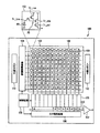
- FIG. 1 is a diagram showing a configuration example of a solid-state image sensor according to the embodiment of the present disclosure.
- the solid-state image sensor 100 is, for example, a CMOS solid-state image sensor.
- the solid-state imaging device 100 includes a pixel region 103 in which pixels 102 including a plurality of photoelectric conversion units are regularly arranged in a two-dimensional lattice pattern, and a peripheral circuit unit.
- the pixel area 103 may be referred to as a pixel array 103.
- the pixel 102 has a photoelectric conversion unit and a plurality of pixel transistors.
- the photoelectric conversion unit is composed of a photodiode PD.
- the pixel transistor includes a transfer transistor Tr_tra, a reset transistor Tr_res, an amplification transistor Tr_amp, and a selection transistor Tr_sel.
- the transfer transistor Tr_tra, the reset transistor Tr_res, the amplification transistor Tr_amp, and the selection transistor Tr_sel are each composed of MOS transistors.
- the photodiode PD is photoelectrically converted by light incident and has a region for accumulating the signal charge generated by the photoelectric conversion.
- the transfer transistor Tr_tra is a transistor that reads out the signal charge accumulated in the photodiode PD into the floating diffusion (FD) region.
- the reset transistor Tr_res is a transistor for setting the potential in the floating diffusion (FD) region to a specified value.
- the amplification transistor Tr_amp is a transistor for electrically amplifying the signal charge read out in the floating diffusion (FD) region.
- the selection transistor Tr_sel is a transistor for selecting one pixel line and reading the pixel signal to the vertical signal line 109. Although not shown, it is also possible to form a pixel with three transistors omitting the selection transistor Tr_sel and a photodiode PD.
- the source of the transfer transistor Tr_tra is connected to the photodiode PD, and its drain is connected to the source of the reset transistor Tr_res.
- a floating diffusion region FD (corresponding to the drain region of the transfer transistor and the source region of the reset transistor) serving as a charge-voltage conversion means between the transfer transistor Tr_tra and the reset transistor Tr_res is connected to the gate of the amplification transistor Tr_amp.
- the source of the amplification transistor Tr_amp is connected to the drain of the selection transistor Tr_sel.
- the drain of the reset transistor Tr_res and the drain of the amplification transistor Tr_amp are connected to the power supply voltage supply unit. Further, the source of the selection transistor Tr_sel is connected to the vertical signal line 109.
- the peripheral circuit unit includes a vertical drive circuit 104, a column signal processing circuit 105, a horizontal drive circuit 106, an output circuit 107, and a control circuit 108.
- the control circuit 108 generates a clock signal or a control signal that serves as a reference for the operation of the vertical drive circuit 104, the column signal processing circuit 105, the horizontal drive circuit 106, and the like. Then, the control circuit 108 inputs these signals to the vertical drive circuit 104, the column signal processing circuit 105, the horizontal drive circuit 106, and the like.
- the vertical drive circuit 104 is composed of, for example, a shift register.
- the vertical drive circuit 104 sequentially selects and scans each pixel 102 in the pixel area 103 in the vertical direction in row units. Then, the vertical drive circuit 104 supplies a pixel signal based on the signal charge generated in each pixel 102 according to the amount of light received to the column signal processing circuit 105 through the vertical signal line 109.
- the vertical drive circuit 104 is connected to the gate of the transfer transistor Tr_tra, the gate of the reset transistor Tr_res, and the gate of the selection transistor Tr_sel via wiring, respectively.
- the vertical drive circuit 104 can turn each gate on or off by applying a signal to each gate of the transfer transistor Tr_tra, the reset transistor Tr_res, and the selection transistor Tr_sel via wiring. ..
- the operation on the pixel 102 is performed by the following procedure.
- the vertical drive circuit 104 turns on the gate of the transfer transistor Tr_tra and the gate of the reset transistor Tr_res to empty all the charges of the photodiode PD.
- the vertical drive circuit 104 stores the electric charge by turning off the gate of the transfer transistor Tr_tra and the gate of the reset transistor Tr_res.
- the vertical drive circuit 104 resets the potential of the floating diffusion region FD by turning on the gate of the reset transistor Tr_res immediately before reading the charge of the photodiode PD.
- the vertical drive circuit 104 turns off the gate of the reset transistor Tr_res, turns on the gate of the transfer transistor Tr_tra, and transfers the electric charge from the photodiode PD to the floating diffusion region FD.
- the amplification transistor Tr_amp the signal charge is electrically amplified in response to the charge applied to the gate.
- the vertical drive circuit 104 turns on the gate of the selection transistor Tr_sel and outputs the image signal charged-voltage converted by the amplification transistor Tr_amp to the vertical signal line 109.
- the column signal processing circuit 105 is arranged for each row of pixels 102.
- the column signal processing circuit 105 performs processing for removing fixed pattern noise peculiar to the pixel 102, and signal processing such as signal amplification and AD conversion.
- the output stage of the column signal processing circuit 105 is connected to the horizontal signal line 110 via a horizontal selection switch (not shown).
- the horizontal drive circuit 106 is composed of, for example, a shift register. The horizontal drive circuit 106 selects each of the column signal processing circuits 105 in order, and causes each of the column signal processing circuits 105 to output a pixel signal to the horizontal signal line 110.
- the output circuit 107 performs signal processing on signals sequentially supplied from each of the column signal processing circuits 105 through the horizontal signal line 110 and outputs the signals.
- the output circuit 107 may only be buffered, or black level adjustment, column variation correction, various digital signal processing, and the like may be performed.
- the input / output terminal 112 exchanges signals with the outside.
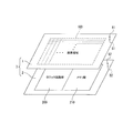
- FIG. 2 is a schematic view showing a configuration example of the solid-state image sensor 100 according to the embodiment of the present disclosure.
- the solid-state imaging device 100 includes a pixel chip 1 and a logic memory chip 2 (hereinafter, referred to as “LM chip 2”) laminated on the pixel chip 1.
- LM chip 2 logic memory chip 2
- the pixel chip 1 is provided with a pixel region 103 having a plurality of pixels 102 on the first main surface S1 side, which is one surface side thereof. Further, although not shown, a color filter and a microlens corresponding to each pixel 102 are provided on the first back surface B1 side.
- the LM chip 2 has a logic circuit unit 200 having a logic circuit for executing various signal processes related to the operation of the solid-state image sensor 100 on the second main surface S2 side, which is one surface side thereof, and a non-volatile memory.
- a memory unit 210 is provided.
- the logic circuit unit 200 includes, for example, any one or more of the vertical drive circuit 104, the column signal processing circuit 105, the horizontal drive circuit 106, the output circuit 107, and the control circuit 108 shown in FIG. 1 as the logic circuit. ..
- the LM chip 2 not only the LM chip 2 but also the pixel chip 1 may be provided with a part of the logic circuit.
- the vertical drive circuit 104, the column signal processing circuit 105, and the control circuit 108 may be provided on the pixel chip 1.
- the non-volatile memory includes, for example, a reluctance change memory, a ferroelectric memory, a phase change memory, a resistance change memory, and the like.
- the pixel chip 1 corresponds to the first structure described in the claims
- the LM chip 2 corresponds to the second structure described in the claims.
- the pixel chip 1 and the LM chip 2 are a first main surface S1 which is a surface on the side where the pixel region 103 of the pixel chip 1 is formed, and a logic circuit unit 200 and a memory unit 210 of the LM chip 2. Is joined to the second main surface S2, which is the surface on which the is formed, via an interlayer insulating film. In this way, the pixel chip 1 and the LM chip 2 are laminated by joining the main surface sides of both. As a result, the joint portion C is formed. This joining method is generally called Face to Face joining. Further, in the present embodiment, the structure in which the pixel chip 1 and the LM chip 2 are bonded together is referred to as a laminated chip 3. In FIG.
- a configuration in which the main surfaces of the pixel chip 1 and the LM chip 2 are joined to each other to stack the two is given as an example, but the configuration is not limited to this configuration, and the first pixel chip 1 is not limited to this configuration.
- the main surface S1 and the second back surface B2 of the LM chip 2 may be joined and laminated.
- the structure is not limited to this, and a three-layer or more layered structure may be used.
- a three-layer configuration in which a pixel chip 1, a logic chip provided with only the logic circuit unit 200, and a memory chip provided with only the memory unit 210 may be laminated may be used.
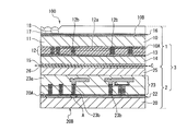
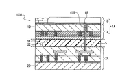
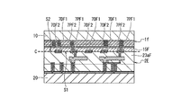
- the solid-state image sensor 100 shown in FIG. 3 is, for example, a back-illuminated CMOS solid-state image sensor. As shown in FIG. 3, the solid-state image sensor 100 includes a pixel chip 1 having a pixel region 103 and an LM chip 2 having a logic circuit unit 200 and a memory unit 210. The first main surface S1 of the pixel chip 1 is bonded to the second main surface S2 of the LM chip 2 to form the laminated chip 3.
- the pixel chip 1 includes a first semiconductor substrate 10.
- the first semiconductor substrate 10 is made of silicon.
- the first semiconductor substrate 10 is provided with a well region 11, a plurality of photodiodes serving as photoelectric conversion units, and a plurality of pixel transistors.
- the pixel transistor includes a transfer transistor Tr_tra, a reset transistor Tr_res, an amplification transistor Tr_amp, and a selection transistor Tr_sel.
- a photodiode and a pixel transistor are provided in the well region 11.
- the first semiconductor substrate 10 may be provided with a plurality of MOS transistors forming a part of the logic circuit unit 200.
- a multilayer wiring layer 12 is provided on the surface (lower surface in FIG. 3) 10A side of the first semiconductor substrate 10.
- the multilayer wiring layer 12 has an interlayer insulating film 12a and a plurality of multilayer wirings 12b arranged in multiple layers via the interlayer insulating film 12a. That is, each of the plurality of multilayer wirings 12b is insulated by the interlayer insulating film 12a.
- the multilayer wiring 12b is made of, for example, copper (Cu) or gold (Au).
- the multilayer wiring 12b is formed by a single damascene method or a dual damascene method.
- a flattening layer 16 is provided on the back surface (upper surface in FIG. 3) 10B side of the first semiconductor substrate 10. Although not shown, the flattening layer 16 has an insulating film, a light-shielding film provided via the insulating film, and a flattening film provided on the insulating film. The light-shielding film is covered with a flattening film. A color filter layer 17 and a microlens 18 are provided on the flattening layer 16.
- a gate electrode is provided on the surface 10A side of the first semiconductor substrate 10 via a gate insulating film.
- a pixel transistor is composed of a gate insulating film, a gate electrode, and a source / drain region. Each unit pixel is separated by, for example, an element separation region (not shown) having an STI (Shallow Trench Isolation) structure.
- the photodiode is composed of, for example, an n-type semiconductor region and a p-type semiconductor region.
- an interlayer insulating film 13 is provided on the multilayer wiring layer 12, and an interlayer insulating film 14 for adjusting the warp of the pixel chip 1 is provided on the interlayer insulating film 13.
- An interlayer insulating film 15 for bonding is provided on the interlayer insulating film 14.
- the pixel transistor and the multi-layer wiring 12b and the wiring portions adjacent to each other in the vertical direction are electrically connected via conductive vias. Further, electrodes are electrically connected to any one of the plurality of wiring portions constituting the multilayer wiring 12b.
- This electrode is configured to electrically connect the pixel transistor of the pixel chip 1 with the logic circuit unit 200 and the memory unit 210 of the LM chip 2. Examples of the electrodes include through electrodes such as TSVs (Through Silicon Vias) and metal electrodes used for direct bonding between chips such as Cu-Cu (copper copper) bonding.
- the LM chip 2 includes a second semiconductor substrate 20.
- the second semiconductor substrate 20 is made of silicon.
- a logic memory mixed layer (hereinafter referred to as "LM mixed layer") 22 in which a logic circuit unit 200 and a memory unit 210 are formed on the surface (upper surface in FIG. 3) 20A side of the second semiconductor substrate 20. Is provided.
- the LM mixed loading layer 22 includes transistors, storage elements 8, electrodes and the like (not shown in FIG. 3) that constitute the logic circuit unit 200 and the memory unit 210.
- a multilayer wiring layer 23 is provided on the LM mixed loading layer 22.
- the multilayer wiring layer 23 has an interlayer insulating film 23a and a plurality of multilayer wirings 23b arranged in multiple layers via the interlayer insulating film 23a.
- An interlayer insulating film 25 for adjusting the warp of the LM chip 2 is provided on the multilayer wiring layer 23.
- An interlayer insulating film 26 for bonding is provided on the interlayer insulating film 25.
- the pixel chip 1 and the LM chip 2 are a bonding surface (lower surface in FIG. 3) of the interlayer insulating film 15 which is the first main surface S1 of the pixel chip 1 and a second surface of the LM chip 2. It is laminated by joining the bonding surface (upper surface in FIG. 3) of the interlayer insulating film 26 which is the main surface S2 of the above.
- Examples of the chip joining method include plasma joining and joining with an adhesive, but in the present embodiment, plasma joining is used.
- plasma bonding the temperature resistance of the MTJ element is taken into consideration, and plasma activation bonding is used. That is, the bonding surface of the pixel chip 1 and the LM chip 2 is subjected to plasma activation treatment, and the two are overlapped and temporarily bonded at room temperature, and then annealed (heat treatment) is performed at 350 ° C to 450 ° C. As a result, both are firmly joined.
- a copper pad is provided so that the surface (bonding surface) is exposed from the facing surface (bonding interface) of the interlayer insulating film 15 and the interlayer insulating film 26.
- a joining method in which copper pads are directly joined to each other. With this Cu-Cu junction, it is possible to also serve as an electrical connection between the chips.
- the interlayer insulating films 12a, 13 to 15, 23a, 25, and 26 are silicon oxide films (SiO2 film, SiO2H film, SiOCH film, etc.) or silicon nitride films (SiN film, SiNH film, etc.).
- the interlayer insulating films 11a, 13, 15, 23a and 26 are silicon oxide films
- the interlayer insulating films 14 and 25 are silicon nitride films.
- the logic circuit unit 200 has a plurality of MOS transistors 201 including CMOS transistors and a plurality of contacts 202 arranged via an interlayer insulating film 220. In addition, it has a plurality of contacts 203 arranged via the interlayer insulating film 221.
- the contact 202 is provided so as to penetrate the interlayer insulating film 220 in the depth direction, and one end portion (lower end portion in FIG. 4) is connected to one of the diffusion regions of each MOS transistor 201 and the other end portion (FIG. 4). In No. 4, the upper end portion) is connected to one end portion (lower end portion in FIG. 4) of the contact 203.
- the contact 203 is provided so as to penetrate the interlayer insulating film 221 in the depth direction, and the other end (upper end in FIG. 4) is one end of the metal wiring 204 (in FIG. 4) forming the multilayer wiring 23b. It is connected to the lower end).
- the memory unit 210 has a memory cell array in which a plurality of memory cells are arranged in a two-dimensional grid pattern. Each memory cell has a storage element 8, a selection transistor 211, and a contact 212. The contact 212 electrically connects one of the diffusion regions of the selection transistor 211 to the storage element.
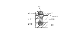
- the memory unit 210 further includes an upper protective film 4T that covers one end surface (upper end surface in FIG. 4) of the storage element 8, a side protective film 4S that covers the side surface of the storage element 8, and a conductive via 213. ing.
- the conductive via 213 electrically connects the storage element 8 and the multilayer wiring 23b.
- the first semiconductor substrate 10 corresponds to the first substrate described in the claims
- the second semiconductor substrate 20 corresponds to the second substrate described in the claims.
- the upper protective film 4T corresponds to the first protective film described in the claims
- the side protective film 4S corresponds to the second protective film described in the claims.
- the selection transistor 211 is arranged via an interlayer insulating film 220 and is composed of a MOS transistor.
- the contact 212 is provided so as to penetrate the interlayer insulating film 220 in the depth direction.
- One end (upper end in FIG. 4) of the contact 212 is connected to the other end surface (lower end surface in FIG. 4) of the storage element 8, and the other end (lower end in FIG. 4) is the selection transistor 211. It is connected to one of the diffusion areas of.
- the conductive via 213 is provided by drilling an interlayer insulating film 221 in the depth direction, one end (lower end in FIG. 4) is connected to the upper protective film 4T, and the other end (in FIG. 4). The upper end) is connected to the metal wiring 214.
- a plurality of MOS transistors 201 included in the logic circuit unit 200 and a plurality of selection transistors 211 included in the memory unit 210 are represented as representatives.
- a gate electrode 201G is provided on the logic circuit portion 200 side of the well region 21 via a gate insulating film.
- the MOS transistor 201 is composed of a gate insulating film, a gate electrode 201G, and a source / drain region.
- a gate electrode 211G is provided on the memory portion 210 side of the well region 21 via a gate insulating film.
- the selection transistor 211 is composed of a gate insulating film, a gate electrode 211G, and a source / drain region.
- the transistors are separated by, for example, an element separation region (not shown) having an STI structure.
- the multilayer wiring 23b constituting the multilayer wiring layer 23 includes metal wirings 204 and 205 on the logic circuit unit 200 side and metal wirings 204 and 205 on the memory unit 210 side arranged via the interlayer insulating films 230 and 231 constituting the interlayer insulating film 23a. It has metal wirings 214 and 215.
- the metal wiring 204 one end (lower end in FIG. 4) is connected to the other end (upper end in FIG. 4) of the contact 203, and the other end (upper end in FIG. 4) is the metal wiring 205. It is connected to one end (lower end in FIG. 4).
- One end (lower end in FIG. 4) of the metal wiring 214 is connected to the other end (upper end in FIG. 4) of the conductive via 213, and the other end (upper end in FIG. 4) is the metal wiring 215. Is connected to one end (lower end in FIG. 4).
- the metal wirings 204, 205, 214, and 215 are made of, for example, Cu or Au.
- the contacts 202, 203 and 212 are made of, for example, tungsten (W). Not limited to W, titanium (Ti), platinum (Pt), palladium (Pd), Cu, tungsten titanium (TiW), tungsten nitride (TiNW), tungsten silicide (WSi 2 ), molybdenum silicide (MoSi 2 ). Etc. may be configured. Further, it may be composed of polysilicon doped with impurities, metal silicide, or the like.
- the contacts 202, 203, and 212 may be configured as a plug filled with any of the above materials, or may be configured as a hole in which any of the above materials is formed on the inner wall of the contact hole.
- the conductive via 213 is composed of, for example, Cu or Au.
- the interlayer insulating films 220, 221 and 230, 231 are silicon oxide films or silicon nitride films. As an example, the interlayer insulating films 220, 221 and 230, 231 are all silicon oxide films.
- the pixel chip 1 and the LM chip 2 are the interlayer insulating films 15 and 26 (hereinafter, "silicon oxide film 15 and") constituting the first main surface S1 and the second main surface S2 of each other. 26 ”) are joined by plasma-activated bonding.
- the silicon oxide films 15 and 26 in the bonded state are vertically sandwiched by the interlayer insulating films 14 and 25 (hereinafter, referred to as "silicon nitride films 14 and 25"). That is, the annealing process is performed in this sandwiched state. In the annealing treatment, for example, a thermal history of 400 ° C. is applied to the silicon oxide films 15 and 26.
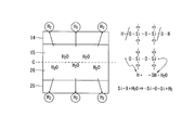
- the silicon oxide films 15 and 26 are insulating films containing a large amount of silanol groups (-OH). Further, the silicon nitride films 14 and 25 are insulating films having excellent moisture resistance. Therefore, when such a heat history of 400 ° C, water from the silicon oxide film 15 and 26 (H 2 O) is disengaged. Then, the separated water is trapped by the silicon nitride films 14 and 25, so that it cannot diffuse outward. In this way, the water sealed due to the process with a high thermal history is steamed (high pressure). At that time, as shown in the following reaction formula (1), the oxidation reaction is promoted and activated hydrogen (H 2 ) is generated. This phenomenon is the high temperature steam cross-link phenomenon.
- H 2 activated hydrogen
- activated hydrogen penetrates the silicon nitride films 14 and 25 as shown in FIG. This hydrogen also penetrates the multilayer wiring layer 23 and reaches the LM mixed loading layer 22.
- the film configuration that can be the source of the high-temperature steam cross-link phenomenon exists in the multilayer wiring layers 12 and 23 as well as the film configuration in the vicinity of the joint portion C.
- the laminated structure of the silicon oxide films 15 and 26 and the silicon nitride films 14 and 25 in the vicinity of the junction C is dominant for the deterioration of the characteristics of the storage element 8.
- the storage element 8 is composed of an MTJ element having heat resistance (up to 400 ° C.).
- the storage element 8 is referred to as an MTJ element 8.
- the MTJ element 8 is made of a magnetic material having vertical magnetic anisotropy.
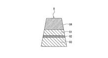
- the MTJ element 8 includes a free layer (also referred to as a storage layer, a recording layer, a magnetization inversion layer, a magnetization free layer, or a Magnetic Free Layer) 81 having a variable magnetization direction.
- a pin layer also called a magnetized fixed layer, also called a Magnetic Pinned Layer
- a tunnel barrier layer also called a tunnel insulating layer
- the MTJ element 8 has a bottom pin structure in which a pin layer 83 is formed on a lower electrode (contact 212) and a free layer 81 is formed on the pin layer 83 via a tunnel barrier layer 82. ing.
- the structure is not limited to this, and a top pin structure may be used in which the free layer 81 is formed on the lower electrode and the pin layer 83 is formed on the free layer 81 via the tunnel barrier layer 82.
- the MTJ element 8 is connected to the selection transistor 211, and an NMOS type FET is usually used as the selection transistor 211.
- the MTJ element 8 When the magnetization direction of the free layer 81 is parallel to the magnetization direction of the pin layer 83, the MTJ element 8 is in a low resistance state, and when it is antiparallel, the MTJ element 8 is in a high resistance state. This difference in resistance state is used for storing information.
- the free layer 81 is composed of, for example, a magnetic metal film containing cobalt (Co), iron (Fe), or the like as main components.
- the free layer 81 is composed of an alloy of Co, Fe and boron (B) (hereinafter, referred to as "CoFeB alloy").
- the tunnel barrier layer 82 is made of, for example, magnesium oxide (MgO), aluminum oxide (AlO), or the like.
- the tunnel barrier layer 82 is composed of magnesium oxide (MgO). By forming the tunnel barrier layer 82 from the MgO layer, the rate of change in magnetic resistance (MR ratio) can be increased.
- the pin layer 83 is made of the same magnetic metal film as the free layer 81. That is, in the first embodiment, the pin layer 83 is made of a CoFeB alloy.
- the upper electrode 84 is composed of, for example, tantalum (Ta), Al, Cu, W, and the like.
- the upper electrode 84 is composed of Ta.
- the MTJ element 8 having such a configuration is affected by the active hydrogen generated by the high-temperature steam cross-link phenomenon, and for example, a reduction reaction of MgO occurs and the magnetic characteristics deteriorate.
- the active hydrogen not only penetrates from the side surface of the MTJ element 8, but also penetrates Ta, Al, Cu, W and the like used for the upper electrode 84. Therefore, it is necessary to prevent hydrogen from entering from the side surface and the upper surface of the MTJ element 8.
- a conductive upper protective film 4T having a property of inhibiting the invasion of hydrogen is formed on the upper surface of the MTJ element 8 (upper surface of the upper electrode 84), and hydrogen invades the side surface of the MTJ element 8. It forms an insulating side protective film 4S having a property of inhibiting the above.
- the memory unit 210 is manufactured by using various devices such as a film forming apparatus (including a CVD (Chemical Vapor Deposition) apparatus and a sputtering apparatus), a heat treatment apparatus, a lithography apparatus, an etching apparatus, and a CMP (Chemical Mechanical Polishing) apparatus. ..
- a film forming apparatus including a CVD (Chemical Vapor Deposition) apparatus and a sputtering apparatus
- a heat treatment apparatus e.g., a lithography apparatus
- an etching apparatus e.g., a CMP (Chemical Mechanical Polishing) apparatus.
- CMP Chemical Mechanical Polishing
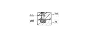
- the manufacturing apparatus uses a plasma CVD method to form an interlayer insulating film 220 made of a silicon oxide film (hereinafter, "" Silicon oxide film 220 ") is formed. After that, the silicon oxide film 220 is penetrated in the depth direction (vertical direction in FIG. 7A) on the diffusion region (here, the source region 211S) of the selection transistor 211 by using lithography, etching, plasma CVD method, or the like. Form contact 212. In the first embodiment, the contact 212 is composed of, for example, W.
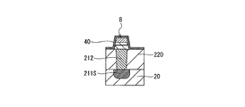
- the manufacturing apparatus forms the MTJ element 8 on the contact 212 by a well-known method, and then insulates the MTJ element 8 on the silicon oxide film 220 including the upper surface and the side surface by the plasma CVD method.
- the film 40 is formed on the entire surface, for example, about 30 [nm].
- the insulating film 40 is a film for forming the side protective film 4S, and is formed of an insulating material having a property of inhibiting the invasion of active hydrogen in the first embodiment. Specifically, in the first embodiment, it is formed from a silicon nitride film.
- the insulating film 40 is referred to as a silicon nitride film 40.
- the insulating film 40 is not limited to the silicon nitride film, and may be formed from a film of another material as long as it has the same function.
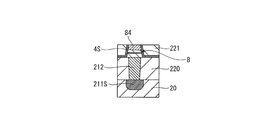
- the manufacturing apparatus uses a plasma CVD method to form an interlayer insulating film 221 (hereinafter, referred to as “silicon oxide film 221”) made of a silicon oxide film on the silicon nitride film 40, for example, 500. [Nm] is formed.
- the manufacturing apparatus uses a CMP apparatus to remove the silicon oxide film 221 until the silicon nitride film 40 on the MTJ element 8 is exposed.
- the silicon nitride film 40 on the MTJ element 8 is removed by anisotropic etching until the upper surface of the upper electrode 84 is exposed. As a result, the portion of the silicon nitride film 40 that covers the side surface of the MTJ element 8 becomes the side protective film 4S.
- the manufacturing apparatus forms, for example, 30 [nm] of a metal film to be the upper protective film 4T on the silicon oxide film 221 including the upper surface of the upper electrode 84 by the sputtering method.
- the metal film is patterned into a desired shape using a lithography apparatus, and then the upper protective film 4T is formed by etching.
- the upper protective film 4T is formed of a conductive metal material having a function of inhibiting the invasion of hydrogen into the MTJ element 8.
- the upper protective film 4T is composed of palladium (Pd), which is one of the metals having a function of storing hydrogen (hereinafter, referred to as "hydrogen storage metal").
- hydrogen storage metals such as Ti, Mg, Ni, vanadium (V), manganese (Mn), zirconium (Zr), and iridium (Ir) may be contained, and these may be contained. It may contain any of the alloys of.
- the shape of the upper protective film 4T is formed, for example, in a rectangular shape, a circular shape, or the like in a plan view.
- the upper protective film 4T includes the entire upper surface (end surface on the joint C side) of the upper electrode 84 in a plan view and surrounds the upper surface within a range not short-circuited with other adjacent MTJ elements 8. It is formed in a shape that makes it. In the first embodiment, it is formed so as to cover at least the entire upper surface of the upper electrode 84 and the upper surface of the side protective film 4S and a range including the periphery thereof, and is formed as large as possible within a range not short-circuited.
- the upper protective film 4T corresponds to the first protective film described in the claims
- the side protective film 4S corresponds to the second protective film described in the claims.
- the manufacturing apparatus forms a via hole on the upper protective film 4T of the silicon oxide film 221 by lithography and etching, and then a barrier layer and a seed layer are formed in the via hole by the film forming apparatus.
- a wiring material for example, Cu or Au
- a CMP apparatus to form a conductive via 213.
- an interlayer insulating film 230 (hereinafter, referred to as “silicon oxide film 230”) made of a silicon oxide film is formed on the silicon oxide film 221 by using a plasma CVD method.
- a trench (wiring groove) is formed in the silicon oxide film 230 on the conductive via 213 by lithography and etching, and then a barrier layer and a seed layer are formed in the trench by a film forming apparatus.
- a wiring material for example, Cu or Au
- a CMP apparatus flattened by a CMP apparatus to form a metal wiring 214.
- the barrier layer is formed to prevent the material (for example, Cu or Au) forming the electrode portion formed in the via hole or the trench from diffusing around the electrode portion.
- the barrier layer is composed of, for example, tantalum (Ta), tantalum nitride (TaN), titanium (Ti), titanium nitride (TiN), or an alloy film containing these.
- the seed layer is an electrode layer for supplying a current during plating.
- the seed layer is composed of, for example, Cu or Au.
- the manufacturing apparatus forms a plurality of interlayer insulating films such as the interlayer insulating film 230 and 231 and a plurality of layers of metal wiring constituting the multilayer wiring 23b such as the metal wiring 215 on the metal wiring 214.
- the manufacturing method has been described focusing on one memory cell, the same manufacturing method is applied to all the memory cells constituting the memory unit 210.
- each step is performed for each of a plurality of memory cells or for all memory cells in parallel.
- the solid-state imaging device 100 determines the amount of charge generated by the photoelectric conversion formed on the first semiconductor substrate 10 and the first semiconductor substrate 10.
- a pixel chip 1 having a pixel region 103 in which a plurality of pixels 102 that output corresponding pixel signals are arranged in a two-dimensional lattice pattern, a pixel chip 1, and a second semiconductor substrate 20 and a second
- a logic memory chip 2 having a logic circuit unit 200 and a memory unit 210 (composed of a non-volatile memory) formed on the semiconductor substrate 20 of 2 is provided.
- An upper protective film 4T having a property of inhibiting the invasion of hydrogen is formed on the end surface of the storage element 8 constituting each memory cell of the memory unit 210 on the side facing the pixel chip 1. Further, a side protective film 4S having a property of inhibiting the invasion of hydrogen is formed on the side surface of the storage element 8.
- the upper protective film 4T provided on the end surface of the storage element 8 on the junction surface side and the side protective film 4S provided on the side surface of the storage element 8 adversely affect the storage element 8 such as hydrogen.
- the side surfaces of atoms and molecules it is possible to prevent the invasion from the end surface (upper end surface in the first embodiment) on the joint surface side.
- the memory unit 210 includes a magnetic tunnel junction element (MTJ element) 8 having heat resistance as a storage element 8, a selection transistor 211, and one of the diffusion regions of the selection transistor 211 (for example, a source region).
- MTJ element magnetic tunnel junction element
- 211S is a magnetoresistive change memory having a contact 212 connecting the MTJ element 8.
- the MTJ element 8 is provided in the vicinity of the selection transistor 211 (in the first embodiment, directly above the contact 212).
- the non-volatile memory constituting the memory unit 210 is composed of the magnetic resistance change memory having the MTJ element 8, the memory unit 210 has a higher density, lower power consumption, and lower leakage. Is possible. Further, since the MTJ element 8 having heat resistance is provided in the vicinity of the selection transistor 211, it is possible to improve the function of the memory unit 210.
- the upper protective film 4T is a metal film composed of a hydrogen storage metal.
- the upper protective film 4T is composed of one or a plurality of hydrogen storage metals, for example, titanium, magnesium, nickel, palladium, vanadium, manganese, zirconium, and iridium. It is a metal film.
- the upper protective film 4T is provided on the upper electrode 84 forming the upper end surface of the MTJ element 8.
- active hydrogen coming from the upper end surface side of the MTJ element 8 is occluded by the upper protective film 4T to the MTJ element 8 without interfering with the energization of the upper electrode 84, for example, by the high temperature steam cross link phenomenon. It becomes possible to prevent the arrival of. As a result, it is possible to prevent or reduce the deterioration of the MTJ element 8 due to atoms or molecules such as active hydrogen.
- the upper protective film 4T has an area larger than the area of the upper end surface of the MTJ element 8.
- the upper end surface is formed so as to include the entire upper end surface inside and surround the upper end surface within a range not short-circuited with other adjacent elements. In the first embodiment, it is formed as large as possible within a range not short-circuited with another adjacent MTJ element 8.
- the conductive via 213 has a diameter of the upper electrode 84 in order to reduce the contact resistance.
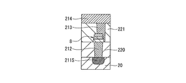
- the size of the diameter is made as large as possible. Therefore, if the forming positions of the conductive vias 213 are misaligned, as shown in FIG. 8B, there is a possibility that the free layer 81 and the pin layer 83 may be short-circuited via the conductive vias 213. It was. It is possible to reduce the diameter of the conductive via 213, but this is not preferable because the contact resistance increases.
- the side surface of the MTJ element 8 is covered with the side protective film 4S having an insulating property, but the conductive via 213 penetrates the side protective film 4S due to misalignment. It is formed by, and there is a risk that a short circuit cannot be avoided.
- the upper protective film 4T surrounds the upper end surface in a plan view within a range not short-circuited with the other adjacent MTJ elements 8. Formed as large as possible.
- the upper protective film 4T can receive the conductive via 213, and the free layer 81 and the pin layer 83 can be received. It is possible to avoid the problem of short-circuiting with and.
- the pixel chip 1 is formed with a plurality of pixel transistors forming a pixel region 103 and a multilayer wiring layer 12 on the first main surface S1 side, which is one surface side thereof.
- An interlayer insulating film 15 for bonding is formed on these upper layers.
- the logic memory chip 2 has a logic circuit unit 200, a memory unit 210, and a multilayer wiring layer 23 formed on the second main surface S2 side, which is one surface side thereof, and is on the upper layer thereof.
- An interlayer insulating film 26 for bonding is formed.
- the pixel chip 1 and the logic memory chip 2 are laminated by joining the interlayer insulating films 15 and 26 formed on the first main surface S1 side and the second main surface S2 side, respectively.
- the first main surface S1 provided with the pixel region 103 of the pixel chip 1 and the second main surface S2 provided with the logic circuit unit 200 and the memory unit 210 of the LM chip 2 was joined to form a laminated chip 3.
- Modification 1 of the first embodiment In the above-described first embodiment, the configuration in which the MTJ element 8 is provided directly above the contact 212 has been described. Modification 1 of the first embodiment is different from the first embodiment in that the MTJ element 8 is not formed directly above the contact 212.
- a lower electrode 85 having a width larger than the width of the MTJ element 8 (the left and right widths in FIG. 10A) is provided above the contact 212. Then, the MTJ element 8 is formed at a position on the lower electrode 85 away from the contact 212.
- the lower electrode 85 may be made of the same material as the upper electrode 84, or may be made of a different material as long as it is a conductive material.
- the upper protective film 4T is included in the entire upper end surface of the MTJ element 8 and the upper end portion of the side protective film 4S in a plan view, and is not short-circuited with other adjacent elements. An example of the size of these surroundings was explained.
- the modified example 2 of the first embodiment is different from the first embodiment in that it is configured to have a size that does not surround the upper end portion of the side protective film 4S in a plan view.
- the upper protective film 4T is formed so as to cover only the entire upper end surface of the MTJ element 8 and the upper end portion of the side protective film 4S.
- the upper protective film 4T may be formed so as to cover only the upper end surface of the MTJ element 8.
- an upper protective film 4T made of a metal film (hereinafter, referred to as “hydrogen storage metal film”) composed of a hydrogen storage metal is provided on the upper end surface of the MTJ element 8 and insulated on the side surface.
- the configuration in which the side protective film 4S made of a film (silicon nitride film) is provided has been described.
- the second embodiment is different from the first embodiment in that a hydrogen storage metal film is also provided on the side surface side of the MTJ element 8.
- the same components as those in the first embodiment will be designated by the same reference numerals, description thereof will be omitted as appropriate, and differences will be described in detail.
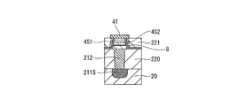
- the side protective film 4S made of an insulating silicon nitride film is provided on the side surface of the MTJ element 8, but as compared with the hydrogen storage metal film, it is caused by the high temperature steam cross-link phenomenon. The ability to prevent the invasion of generated active hydrogen is inferior. Therefore, in the second embodiment, the side protective film 4S2 made of a hydrogen storage metal film is further formed on the side protective film 4S (referred to as “side protective film 4S1” in the second embodiment).
- the memory unit 210 is manufactured using the same manufacturing apparatus as in the first embodiment.
- the steps shown in FIGS. 7A to 7B of the first embodiment are the same, so the description thereof will be omitted, and the following steps will be described.
- the manufacturing apparatus applies, for example, 30 [nm] a hydrogen storage metal film to be the side protective film 4S2 on the entire surface including the portion covering the MTJ element 8 on the silicon nitride film 40 by a sputtering method. Form.
- the manufacturing apparatus performs anisotropic etching so that the hydrogen storage metal film remains only on the side surface side of the MTJ element 8. As a result, the portion of the hydrogen storage metal film that covers the side surface side of the MTJ element 8 becomes the side protective film 4S2.
- the side protective film 4S2 is configured to contain Pd, which is one of the hydrogen storage metals, in the second embodiment. Not limited to Pd, it may be composed of other hydrogen storage metals such as Ti, Mg, Ni, V, Mn, Zr, Ir, etc., or may be composed of any of these alloys. You may.
- the manufacturing apparatus forms, for example, 500 [nm] of a silicon oxide film 221 on the silicon nitride film 40 and the side protective film 4S2 by using the plasma CVD method.
- the manufacturing apparatus removes the silicon oxide film 221 using the CMP apparatus until the upper end surfaces of the silicon nitride film 40 and the side protective film 4S2 on the MTJ element 8 are exposed.
- anisotropic etching is used to remove the silicon nitride film 40 on the MTJ element 8 until the upper surface of the upper electrode 84 is exposed. As a result, the portion of the silicon nitride film 40 that covers the side surface of the MTJ element 8 becomes the side protective film 4S1.
- the manufacturing apparatus forms, for example, 30 [nm] of a metal film to be the upper protective film 4T on the silicon oxide film 221 including the upper electrode 84 and the upper surfaces of the side protective films 4S1 and 4S2 by the sputtering method.
- the metal film is patterned into the same shape as that of the first embodiment by lithography, and then the upper protective film 4T is formed by etching.
- the manufacturing apparatus forms a via hole on the upper protective film 4T of the silicon oxide film 221 by lithography and etching, and then a barrier layer and a seed layer are formed in the via hole by the film forming apparatus.
- a wiring material for example, Cu or Au
- a CMP apparatus to form a conductive via 213.
- an interlayer insulating film 230 (hereinafter, referred to as “silicon oxide film 230”) made of a silicon oxide film is formed on the silicon oxide film 221 by using a plasma CVD method.
- a trench (wiring groove) is formed in the silicon oxide film 230 on the conductive via 213 by lithography and etching, and then a barrier layer and a seed layer are formed in the trench by a film forming apparatus.
- a wiring material for example, Cu or Au
- a CMP apparatus flattened by a CMP apparatus to form a metal wiring 214.
- the manufacturing apparatus forms a plurality of interlayer insulating films such as the interlayer insulating film 230 and 231 and a plurality of layers of metal wiring constituting the multilayer wiring 23b such as the metal wiring 215 on the metal wiring 214.
- the manufacturing method has been described focusing on one memory cell, the same manufacturing method is applied to all the memory cells constituting the memory unit 210. Further, each step is performed for each of a plurality of memory cells or for all memory cells in parallel.
- the upper protective film 4T of the second embodiment includes the entire upper surface of the upper electrode 84, the side protective films 4S1 and 4S2 inside and is not short-circuited with other adjacent MTJ elements 8 in a plan view. Is configured to surround. With this configuration, as shown in FIG. 12, even if the conductive vias 213 are misaligned, they can be received by the upper protective film 4T. As a result, it is possible to prevent a short circuit between the free layer 81 and the pin layer 83 due to misalignment.
- the solid-state imaging device 100 determines the amount of charge generated by the photoelectric conversion formed on the first semiconductor substrate 10 and the first semiconductor substrate 10.
- a pixel chip 1 having a pixel region 103 in which a plurality of pixels 102 that output corresponding pixel signals are arranged in a two-dimensional lattice pattern, a pixel chip 1, and a second semiconductor substrate 20 and a second
- a logic memory chip 2 having a logic circuit unit 200 and a memory unit 210 (composed of a magnetic resistance change memory) formed on the semiconductor substrate 20 of 2 is provided.
- the end surface (upper end surface in the second embodiment) of the MTJ element 8 constituting each memory cell of the memory unit 210 on the side facing the pixel chip 1 is an upper protection made of a metal film composed of a hydrogen storage metal.
- a film 4T is formed.
- an insulating side protective film 4S1 having a property of inhibiting the invasion of hydrogen is formed on the side surface of the MTJ element 8.
- a side protective film 4S2 made of a metal film containing a hydrogen storage metal is formed on the side protective film 4S1.
- the side protective film 4S2 is a metal film composed of, for example, one or a plurality of titanium, magnesium, nickel, palladium, vanadium, manganese, zirconium, and iridium as hydrogen storage metals. Is.
- the upper protective film 4T provided on the end surface of the MTJ element 8 on the junction surface side and the side protective films 4S1 and 4S2 provided on the side surface of the MTJ element 8 adversely affect the MTJ element 8 such as hydrogen. It is possible to prevent not only the invasion of atoms and molecules from the side surface but also the invasion from the end surface on the bonding surface side. In addition, since not only the insulating side protective film 4S1 but also the side protective film 4S2 made of hydrogen storage metal is provided on the side surface side of the MTJ element, the side surfaces of atoms and molecules that adversely affect the MTJ element 8 such as hydrogen are provided. It is possible to more reliably prevent or reduce the invasion from.
- the side protective film 4S2 made of a hydrogen storage metal film is provided on the side protective film 4S1 formed of an insulating silicon nitride film having a property of inhibiting the invasion of hydrogen.
- an insulating film having no property of inhibiting the invasion of hydrogen is provided on the side surface of the MTJ element 8 in place of the side protective film 4S1, and the side protective film 4S2 is provided on the insulating film. Is different from the second embodiment.
- an insulating film having no property of inhibiting the invasion of hydrogen other than the silicon nitride film is formed on the side surface of the MTJ element 8 and is made of a hydrogen storage metal on the insulating film.
- a side protective film 4S2 is provided. Examples of the insulating film having no property of inhibiting the invasion of hydrogen include a silicon oxide film.
- the protective performance is lowered by the amount of the silicon nitride film, but the upper protective film 4T and the side protective film 4S2 allow the upper end surface in addition to the invasion from the side surface of atoms and molecules which adversely affect the memory element 8. It is possible to prevent or reduce the invasion from.
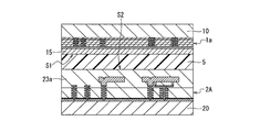
- the solid-state image sensor 100A according to the third embodiment includes a pixel chip 1A and an LM chip 2A.
- the pixel chip 1A according to the third embodiment includes a pixel unit 1a and a lens unit 1b.
- the pixel portion 1a includes a first semiconductor substrate 10 in which pixels such as pixel transistors are formed in a well region 11, a multilayer wiring layer 12, an interlayer insulating film (silicon oxide film) 13, and an interlayer insulating film (silicon oxide film). ) 15 and.
- the interlayer insulating film 13 is formed of a silicon oxide film, and the interlayer insulating film on the LM chip 2A side of the multilayer wiring layer 12 is composed of only a silicon oxide film. That is, the LM chip 2A side of the multilayer wiring layer 12 is not provided with a nitride film such as a silicon nitride film 14 for adjusting the warp, which causes a high temperature steam cross-link phenomenon.
- the lens unit 1b includes a flattening layer 16, a color filter layer 17, and a microlens 18.
- the LM chip 2A has a configuration in which the interlayer insulating film (silicon nitride film) 25 and the interlayer insulating film (silicon oxide film) 26 are removed from the LM chip 2 of the first embodiment.
- the interlayer insulating film on the pixel chip 1A side of the multilayer wiring layer 23 is composed of only a silicon oxide film. That is, similarly to the pixel chip 1A, a nitride film such as a silicon nitride film 25 for warp adjustment, which causes a high temperature steam cross-link phenomenon, is not provided on the pixel chip 1A side of the multilayer wiring layer 23. There is.
- the silicon oxide film 26 is also removed. Not limited to this configuration, the silicon oxide film 26 may be left as an interlayer insulating film for bonding without being removed.
- the end face of the silicon oxide film 15 serving as the first main surface S1 of the pixel chip 1A and the end face of the silicon oxide film 23a serving as the second main surface S2 of the LM chip 2A are formed. It is joined via the adhesive 5.
- the laminated chip 3 (hereinafter, referred to as “laminated chip 3A”) according to the third embodiment in which the pixel chip 1A and the LM chip 2A are laminated is configured.
- the joint portion C1 on the pixel chip 1A side and the joint portion C2 on the LM chip 2A side are formed via the adhesive 5.
- the adhesive 5 is composed of, for example, a resin material.
- the resin material include BCB (Benzocyclobutene) resin, Polyimide (polyimide) resin, Benzoxazole (benzoxazole) resin, Polyarylene (polyarylene) resin and the like. These resin materials have different physical property values, and an appropriate one will be selected according to the process after joining.
- the important characteristics of the adhesive used for bonding semiconductor chips are the heat resistant temperature that can withstand the thermal history of the process after the bonding process, mainly the degassing property during cross-linking, kinematic viscosity, coating film thickness, etc. Is. These are directly linked to product yield.
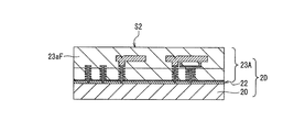
- FIG. 13A the pixel portion 1a and the LM chip 2A having the above configuration are manufactured by a well-known manufacturing method.
- the coating device is used to provide a second main surface S2 (upper end surface in FIG. 13C) which is a joining surface of the silicon oxide film 23a of the LM chip 2A.
- a paste-like resin adhesive 5 is applied onto the entire surface so as to be uniform throughout.
- the method of application is not particularly limited, but for example, application can be performed with a dispenser having a syringe equipped with a precision nozzle or the like.
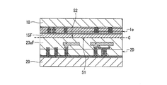
- the first main surface S1 (FIG. 3), which is the bonding surface of the silicon oxide film 15 of the pixel portion 1a, is placed on the coated surface of the adhesive 5 of the LM chip 2A by the bonding device.
- the lower end surface is overlapped and crimped.
- the bonding is completed by heating the adhesive 5 at a temperature and time required for bonding (curing) in a drying device to cure the adhesive 5.
- the method for drying the adhesive 5 is not particularly limited, but for example, the adhesive 5 is cured by applying hot air at 70 to 80 ° C for a predetermined time and then heating at 150 ° C to 220 ° C for a predetermined time. Can be done. That is, in the joining step, the high temperature treatment of 350 ° C to 400 ° C as in the first and second embodiments is not required.
- the lens portion 1b is formed on the back surface 10B of the first semiconductor substrate 10 by a well-known method.
- the laminated chip 3A is formed.
- the chips of the laminated chips 3 are electrically connected to each other before the lens portion 1b is formed. Examples of this connection method include a method of connecting inside the chip by a through silicon via (TSV) and a method of connecting via a joint portion by the above-mentioned Cu-Cu bonding.
- TSV through silicon via
- the connection is made using the TSV.
- the signal lines and the power supply lines formed in the multilayer wiring layers 12 and 23 provided in the pixel chip 1A and the LM chip 2A are electrically connected to each other by the twin contact type TSV6A. Is connected to.
- the TSV 6A is formed by a well-known method, and has a first through electrode 61A that penetrates the first semiconductor substrate 10 from the upper surface of the pixel portion 1a of the pixel chip 1A to reach the multilayer wiring layer 12.
- it has a second through electrode 62A that penetrates the first semiconductor substrate 10 and the multilayer wiring layer 12 from the upper surface of the pixel portion 1a and reaches the multilayer wiring layer 23 of the LM chip 2A.
- it has a through electrode connecting wiring 63A for connecting the first and second through electrodes 61A and 62A. In this way, the signal lines and the power supply lines formed in the multilayer wiring layers 12 and 23 are electrically connected to each other via the two through electrodes (the first through electrode 61A and the second through electrode 62A). ..
- Each through silicon via of TSV6A is formed by the same manufacturing method as the conductive via 213. Further, the example in which the TSV6A is created after stacking the chips has been described, but the present invention is not limited to this, and the TSV6A is created at another timing such as after the pixel chips 1A and the LM chips 2A are created or during the creation of the multilayer wiring layer. You may.
- the pixel chip 1A has a plurality of pixels forming a pixel region 103 on the first main surface S1 side, which is one surface side thereof. A transistor and a multilayer wiring layer 12 are formed, and an interlayer insulating film 15 for bonding is formed on these upper layers.
- the logic memory chip 2A has a logic circuit unit 200, a memory unit 210, and a multilayer wiring layer 23 formed on the second main surface S2 side, which is one surface side thereof, and is on the upper layer thereof. An interlayer insulating film 23a for bonding is formed. Further, the pixel chip 1A and the logic memory chip 2A are laminated by joining the end faces of the interlayer insulating films 15 and 23a, which are the first and second main surfaces S1 and S2, to each other via a resin adhesive 5. Has been done.
- the L / M chip 2A side of the pixel chip 1A is closer to the multilayer wiring layer 12, and the pixel chip is more than the multilayer wiring layer 23 of the L / M chip 2A. Only an oxide film is formed on the 1A side as an interlayer insulating film. That is, on the L / M chip 2A side of the pixel chip 1A from the multilayer wiring layer 12 and on the pixel chip 1A side of the L / M chip 2A from the multilayer wiring layer 23, a silicon nitride film or the like for adjusting the warp of the chip or the like The nitride film is not formed.
- the adhesive 5 is composed of at least one of a BCB resin, a polyimide resin, a benzoxazole resin, and a polyarylene resin.
- the BCB resin has high heat resistance and can be cured by a polymerization reaction using only heat. Therefore, no catalyst or initiator is required, and there are few impurities caused by them.
- volatile substances are not generated during heat curing, for example, condensed water is not generated during the curing of polyimide, there is no concern about corrosion of wiring materials.
- the multilayer wiring 12b of the multilayer wiring layer 12 of the pixel chip 1A and the multilayer wiring 23b of the multilayer wiring layer 23 of the LM chip 2A are in twin contact. It is electrically connected via a TSV (Through Silicon Via) 6A of the mold. With this configuration, since the TSV6A electrically connects the chips, it is possible to improve the degree of freedom in arranging the MTJ element 8. In addition, it is possible to manufacture a laminated chip 3A and thus a solid-state image sensor 100A that does not deteriorate the characteristics of the flexibly arranged MTJ element 8.
- the first modification of the third embodiment is different from the third embodiment in that the connection is performed by the shared contact type TSV. That is, as shown in FIG. 15, the solid-state image sensor 100B according to the first modification has signal lines and power lines formed on the multilayer wiring layers 12 and 23 provided on the pixel chips 1A and the LM chips 2A, respectively. They are electrically connected to each other by a shared contact type TSV6B.
- the shared contact type TSV6B penetrates the first semiconductor substrate 10 from the surface of the pixel portion 1a of the pixel chip 1A and penetrates the multilayer wiring layer 12 while conducting with a part of the multilayer wiring 12b. It has one through electrode 61B provided so as to reach the multilayer wiring layer 23 of the M chip 2A and conduct with a part of the multilayer wiring 23b. Further, the through electrode 61B of the first modification has a structure in which a conductive material is embedded in the through hole. That is, the through silicon via 61B penetrates while exposing a part of the multilayer wiring 12b of the pixel chip 1A, and further penetrates the multilayer wiring layer 23 of the LM chip 2A so as to expose a part of the multilayer wiring 23b.
- a through hole is formed. Then, it is formed by embedding a conductive material (for example, Cu) in the through hole.
- a conductive material for example, Cu
- the structure is not limited to this, and a structure in which a conductive material is formed on the inner wall of the through hole may be used.
- the multilayer wiring layers of the pixel chip 1A and the LM chip 2A share one common through electrode 61B, and electrically connect the signal lines and the power supply lines formed therein.
- laminated chip 3B the laminated chip 3 in which the pixel chips 1A and the LM chips 2A having such a configuration are laminated.
- both the pixel chip 1A and the L / M chip 2A are oxidized as an interlayer insulating film on the L / M chip 2A side of the multilayer wiring layer 12 and on the pixel chip 1A side of the multilayer wiring layer 23.
- the configuration that forms only the film has been described. That is, a configuration has been described in which a nitride film including a silicon nitride film for adjusting the warp of the chip is not provided on the LM chip 2A side of the multilayer wiring layer 12 and on the pixel chip 1A side of the multilayer wiring layer 23.
- only one of the L / M chip 2A side of the pixel chip 1A and the L / M chip 2A and the pixel chip 1A side of the multilayer wiring layer 23 is a nitride film. It is different from the above-mentioned third embodiment in that the configuration is not provided.
- the solid-state imaging device 100A according to the second modification has the configuration shown in FIG. 14, for example, on the LM chip 2A side of the multilayer wiring layer 12 of the pixel chip 1A and the LM chip 2A.
- only one of the pixel chip 1A side of the multilayer wiring layer 23 is formed as an interlayer insulating film and only an oxide film is formed. That is, only one of the L / M chip 2 side of the pixel chip 1A and the L / M chip 2A and the pixel chip 1 side of the multilayer wiring layer 23 does not form a nitride film as an interlayer insulating film. And said.
- the bonding surfaces of the pixel chip 1A and the LM chip 2A having such a configuration are bonded via the adhesive 5.
- this configuration it is possible to suppress the generation of active hydrogen as compared with the configurations of the pixel chip 1 and the LM chip 2 of the first and second embodiments.
- it is possible to facilitate the warp adjustment by providing a silicon nitride film for warp adjustment only on the chip side where the warp becomes larger.
- both the pixel chip 1A and the L / M chip 2A are used for adjusting the warp of the chip on the L / M chip 2A side of the multilayer wiring layer 12 and on the pixel chip 1A side of the multilayer wiring layer 23.
- the configuration in which a nitride film such as a silicon nitride film is not provided has been described. That is, a configuration has been described in which a nitride film including a silicon nitride film for adjusting the warp of the chip is not provided on the LM chip 2A side of the multilayer wiring layer 12 and on the pixel chip 1A side of the multilayer wiring layer 23.
- Modification 3 of the third embodiment is different from the third embodiment in that the pixel chips 1 and LM chips 2 of the first and second embodiments are joined via an adhesive 5. That is, although not shown, the solid-state imaging device 100 according to the third modification has the silicon oxide films 15 and 26 of the pixel chip 1 and the LM chip 2 instead of the plasma activation bonding in the configuration shown in FIG. The joint surface of the above was configured to be joined via the adhesive 5.
- the chip in the configuration of the memory unit 210 of the first and second embodiments, the chip is located on the LM chip 2 side of the multilayer wiring layer 12 and on the pixel chip 1 side of the multilayer wiring layer 23.
- a nitride film such as a silicon nitride film for adjusting the warp is not provided. Then, the configuration in which the pixel chip 1A and the LM chip 2A having such a configuration are joined via the adhesive 5 has been described.
- the configuration of the third embodiment is applied to the configuration in which the protective film is not provided on at least one of the upper surface and the side surface of the MTJ element 8.
- the configuration of the memory cell is, for example, the configuration shown in FIG. 8A. Specifically, a protective film is not formed on both the upper surface and the side surface of the MTJ element 8.
- the pixels are larger than the multilayer wiring layer 12 of the pixel chip 1 and the L / M chip 2A on the L / M chip 2 side and the multilayer wiring layer 23.
- the configuration of joining the bonding surfaces of the interlayer insulating films 15 and 23a of the pixel chip 1A and the LM chip 2A having a structure in which only an oxide film is formed as an interlayer insulating film on the chip 1 side is described via an adhesive 5. ..
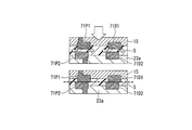
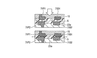
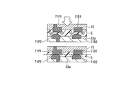
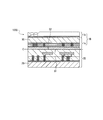
- the fourth embodiment is different from the third embodiment in that the metal electrodes are directly bonded to each other in addition to the bonding by the adhesive 5.
- the same components as those in the third embodiment will be designated by the same reference numerals, description thereof will be omitted as appropriate, and different points will be described in detail.
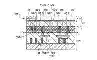
- the solid-state image sensor 100C according to the fourth embodiment includes a pixel chip 1C and an LM chip 2C.
- the pixel chip 1C according to the fourth embodiment includes a pixel unit 1d and a lens unit 1b.
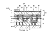
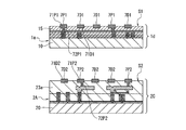
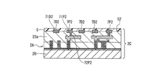
- the pixel portion 1d has a configuration in which the pixel portion 1a of the third embodiment includes a plurality of metal electrodes 7P1 and a plurality of dummy electrodes 7D1 provided on the silicon oxide film 15.
- the metal electrode 7P1 includes a metal electrode pad 71P1 as a joint portion and a metal electrode via 72P1 extending from the metal electrode pad 71P1 and connected to the multilayer wiring 12b.
- the dummy electrode 7D1 includes a metal electrode pad 71D1 as a joint portion.
- the plurality of metal electrodes 7P1 and the plurality of dummy electrodes 7D1 are provided so that at least a part including the pad surfaces (bonding surfaces) of the metal electrode pads 71P1 and 71D1 is exposed from the surface on the bonding side of the silicon oxide film 15. ing.
- the L / M chip 2C has a configuration in which the L / M chip 2A of the third embodiment includes a plurality of metal electrodes 7P2 and a plurality of dummy electrodes 7D2 provided on the silicon oxide film 23a.
- the metal electrode 7P2 includes a metal electrode pad 71P2 as a joint portion and a metal electrode via 72P2 extending from the metal electrode pad 71P2 and connected to the multilayer wiring 23b.
- the dummy electrode 7D2 includes a metal electrode pad 71D2 as a joint portion.
- the plurality of metal electrodes 7P2 and the plurality of dummy electrodes 7D2 are provided so that at least a part including the pad surfaces (bonding surfaces) of the metal electrode pads 71P2 and 71D2 is exposed from the surface on the bonding side of the silicon oxide film 23a. ing.
- the metal electrodes 7P1 and 7P2 are each made of a conductive metal material suitable for direct bonding. Examples of this metal material include Cu, Au, and Al. In the fourth embodiment, it is assumed that it is composed of Cu.
- the dummy electrodes 7D1 and 7D2 are made of the same material as the metal electrodes 7P1 and 7P2, and each has a configuration provided only with the metal electrode pad. That is, the dummy electrodes 7D1 and 7D2 are dummy metal electrodes for increasing the bonding strength, and do not have the role of electrodes.
- the metal electrodes 7P1 and 7P2 and the dummy electrodes 7D1 and 7D2 are paired, respectively, and a plurality of pairs of these are provided. Further, the paired metal electrodes 7P1 and 7P2 and the dummy electrodes 7D1 and 7D2 are provided at positions where at least a part of their respective pad surfaces face each other at the time of joining.
- the metal electrodes 7P1 and 7P2 are formed by, for example, a single damascene method or a dual damascene method, and the dummy electrodes 7D1 and 7D2 are formed by, for example, a single damascene method.
- the metal electrodes 7P1 and 7P2 and the dummy electrodes 7D1 and 7D2 are simply referred to as "metal electrodes 7" when it is not necessary to distinguish them.
- the end surface of the silicon oxide film 23a to be S2 and the pad surface of the metal electrode 7P2 and the dummy electrode 7D2 are joined.
- the metal electrode 7P1 and the dummy electrode 7D1 and the metal electrode 7P2 and the dummy electrode 7D2 are firmly bonded to each other in pairs by direct bonding.
- the opposing portions of the silicon oxide film 15 and the silicon oxide film 23a between these electrodes are joined via an adhesive 5.
- laminated chip 3C (hereinafter, referred to as “laminated chip 3C”) according to the fourth embodiment in which the pixel chip 1C and the LM chip 2C are laminated is configured.
- the pixel portion 1d and the LM chip 2C having the above configuration are manufactured by a well-known manufacturing method.
- the process proceeds to the bonding step, and as shown in FIG. 16C, the second main surface S2, which is the bonding surface of the silicon oxide film 23a of the LM chip 2C and the metal electrode 7P2 and the dummy electrode 7D2, is used by the coating device.
- the adhesive 5 is applied evenly over the entire surface (upper end surface in FIG. 16C).
- the bonding surface of the silicon oxide film 15 of the pixel portion 1d and the metal electrode 7P1 and the dummy electrode 7D1 are formed on the coated surface of the adhesive 5 of the LM chip 2C by the bonding device.
- the first main surface S1 (lower end surface in FIG. 16D) is overlapped and crimped. That is, as shown in FIG. 17, the paired metal electrode pads 71P1 and 71P2 and the paired metal electrode pads 71P1 and 71D2 are pushed out by pushing out the adhesive 5 existing between the 71D1 and 71D2 due to the pressure at the time of joining. Direct bonding between 71P2 and 71D1 and 71D2 is performed.
- the metal electrodes 7 are joined to each other at a relatively low temperature such as room temperature.
- the bonding is completed by heating the adhesive 5 at the temperature and time required for bonding (curing) in a drying device to cure the adhesive 5.
- the lens portion 1b is formed on the back surface 10B of the first semiconductor substrate 10 by a well-known method. As a result, the laminated chip 3C is formed.
- the pixel chip 1C has a plurality of pixels constituting the pixel region 103 on the first main surface S1 side which is one surface side thereof. A transistor and a multilayer wiring layer 12 are formed, and an interlayer insulating film (silicon oxide film) 15 for bonding is formed on these upper layers.
- the logic memory chip 2A has a logic circuit unit 200, a memory unit 210, and a multilayer wiring layer 23 formed on the second main surface S2 side, which is one surface side thereof, and is on the upper layer thereof. An interlayer insulating film (silicon oxide film) 23a for bonding is formed.
- the silicon oxide film 15 is provided with a plurality of metal electrodes 7P1 so that at least a part including the pad surface is exposed on the joint surface side. Further, at a position of the silicon oxide film 23a facing the pad surface of the metal electrode 7P1, a plurality of metal electrodes 7P2 are provided so that at least a part including the pad surface is exposed to the joint surface side. Further, the metal electrodes 7 facing each other between the pixel chip 1C and the LM chip 2C (the bonding surfaces of the paired metal electrode pads 71P1 and 71P2) are directly bonded to each other, and the silicon oxide film 15 and the silicon oxide film 15 and The 23a are joined to each other via the adhesive 5.
- the metal electrodes 7P1 and 7P2 are directly bonded to each other, so that the bonding strength can be increased.
- the connection between the metal electrodes on the joint surface facilitates one-to-one connection between, for example, the pixel 102 and the analog-to-digital conversion circuit (not shown) and the storage element 8, so that analog-to-digital conversion is performed for each pixel 102. It is possible to easily configure a so-called pixel ADC type solid-state image sensor in which the above is performed.
- the silicon oxide film 15 is provided with a plurality of metal electrodes 7P1 having a metal electrode pad 71P1 and a metal electrode via 72P1.
- the silicon oxide film 15 is provided with a plurality of dummy electrodes 7D1 having a metal electrode pad 71D1.
- Each metal electrode 7P1 and dummy electrode 7D1 are provided so that at least a part including a pad surface is exposed from the joint surface of the silicon oxide film 15.
- a plurality of metal electrodes 7P2 having a metal electrode pad 71P2 and a metal electrode via 72P2 are provided at positions of the silicon oxide film 23a facing the plurality of metal electrodes 7P1.
- the silicon oxide film 23a is provided with a plurality of dummy electrodes 7D2 having a metal electrode pad 71D2.
- Each metal electrode 7P2 and dummy electrode 7D2 are provided so that at least a part including a pad surface is exposed from the joint surface of the silicon oxide film 23a.
- the metal electrodes 7 facing each other between the pixel chip 1C and the LM chip 2C (the joint surfaces of the paired metal electrode pads 71P1 and 71P2, and the paired metal electrode pads 71D1 and 71D2) Are directly joined.
- the bonding surfaces of the silicon oxide films 15 and 23a are bonded to each other via an adhesive 5 composed of a resin material.
- dummy electrodes 7D1 and 7D2 are provided so that they can be directly bonded to each other, so that the bonding strength can be further increased.
- the L / M chip 2C side of the multi-layer wiring layer 12 of the pixel chip 1C and the pixel chip 1C of the multi-layer wiring layer 23 of the L / M chip 2C Only an oxide film is formed on the side as an interlayer insulating film. That is, on the L / M chip 2C side of the pixel chip 1C from the multilayer wiring layer 12 and on the pixel chip 1C side of the L / M chip 2C from the multilayer wiring layer 23, a silicon nitride film or the like for adjusting the warp of the chip or the like The nitride film is not formed.
- the adhesive 5 is composed of at least one of a BCB resin, a polyimide resin, a benzoxazole resin, and a polyarylene resin.
- the surface is formed in a convex shape. That is, in the solid-state image sensor 100C according to the first modification, as shown in FIG. 18, the shapes of the joint surfaces of the metal electrodes 7P1 and the dummy electrodes 7D1 formed on the pixel chip 1C side are joined. It is formed in a convex shape in the direction (downward in FIG. 18).
- the convex shape of the metal electrode pads 71P1 and 71D1 on the pixel chip 1C side improves the extruding performance of the adhesive 5 from between the metal electrode pads 71P1 and 71P2 and 71D1 and 71D2 at the time of crimping. Is possible. This makes it possible to facilitate direct bonding between the metal electrodes 7 during the crimping process, and makes it possible to eliminate the need for additional high-temperature processing.
- the solid-state image sensor 100C according to the second modification has the shape of the joint surface of the metal electrode pads 71P2 and 71D2 of the metal electrodes 7P2 and the dummy electrodes 7D2 formed on the LM chip 2C side. Is formed to be convex toward the joining direction (upward in FIG. 19).
- the convex shape of the metal electrode pads 71P2 and 71D2 on the LM chip 2C side improves the extruding performance of the adhesive 5 from between the metal electrode pads 71P1 and 71P2 and 71D1 and 71D2 at the time of crimping. It becomes possible. This makes it possible to facilitate direct bonding between the metal electrodes 7 during the crimping process, and makes it possible to eliminate the need for additional high-temperature processing.
- Modification 3 of the fourth embodiment In the first and second modifications of the fourth embodiment, the configuration in which the joint surface of one of the metal electrode pads 71 of the paired metal electrodes 7 has a convex shape has been described.
- the third modification of the fourth embodiment is different from the first and second modifications of the fourth embodiment in that both of the joint surfaces of the metal electrode pads 71 of the paired metal electrodes 7 are formed in a convex shape.
- the shape of the bonding surface of the metal electrode pads 71P1 and 71D1 formed on the pixel chip 1C side is in the bonding direction (downward in FIG. 20).
- the shape of the joint surface of the metal electrode pads 71P2 and 71D2 formed on the L / M chip 2C side is formed to be convex toward the joint direction (upward in FIG. 20).
- Modification 4 of the fourth embodiment In the fourth embodiment described above, a configuration has been described in which the joint surfaces of the paired metal electrodes 7 are directly joined by crimping each other. Modification 4 of the fourth embodiment is different from the fourth embodiment in that an additional annealing treatment (high temperature treatment) is performed after the crimping treatment between the metal electrodes 7 at a relatively low temperature such as room temperature.
- an additional annealing treatment high temperature treatment
- the adhesive 5 may not be completely pushed out from between the paired metal electrodes 7 in the crimping process by the bonding device, and after the crimping process.
- an annealing treatment high temperature treatment
- the thickness of the adhesive 5 at the time of crimping between the paired metal electrodes 7 is controlled to 15 [nm] or less. By controlling the thickness to 15 [nm] or less, it is possible to realize solid phase diffusion bonding between the metal electrodes 7.
- the additional heat treatment promotes the hillock growth of the joint surface of the metal electrode 7, causes the metal electrode 7 to break through the resin layer of the adhesive 5, and causes the metal electrodes 7 to perform solid-phase diffusion bonding.
- the metal electrodes 7 can be joined more reliably, and the joining strength can be further increased.
- the pixel chip 1C and the LM chip 2C are not formed with a silicon nitride film for adjusting the warp of the chip. Therefore, the high-temperature steam cross-link phenomenon itself does not occur, the generation of active hydrogen can be suppressed, and the desorbed hydrogen from the silicon nitride film does not occur.
- the pixel chip 1 and the LM chip 2A have more pixels than the LM chip 2 side and the multilayer wiring layer 23 than the multilayer wiring layer 12.
- the configuration in which the pixel chip 1A and the LM chip 2A having a structure in which only an oxide film is formed as an interlayer insulating film on the chip 1 side are joined via an adhesive 5 has been described.
- the fifth embodiment is different from the third embodiment in that the silicon oxide films 15 and 23a are directly bonded to each other without using the adhesive 5 in the configuration of the third embodiment.
- the same components as those in the third embodiment will be designated by the same reference numerals, description thereof will be omitted as appropriate, and different points will be described in detail.
- the solid-state image sensor 100D according to the fifth embodiment includes a pixel chip 1D and an LM chip 2D.
- the pixel chip 1D according to the fifth embodiment includes a pixel unit 1e and a lens unit 1b.
- the pixel portion 1e has a configuration in which the silicon oxide film 15F is provided in place of the silicon oxide film 15 in the pixel portion 1a of the third embodiment.
- the LM chip 2D has a configuration in which the silicon oxide film 23aF is provided in place of the silicon oxide film 23a in the LM chip 2C of the third embodiment.
- the silicon oxide films 15F and 23aF are designed so that the warp becomes flat during the BEOL process.
- the end surface of the silicon oxide film 15 serving as the first main surface S1 of the pixel chip 1D and the end surface of the silicon oxide film 23a serving as the second main surface S2 of the LM chip 2D are formed. It is directly joined.
- the laminated chip 3 (hereinafter, referred to as “laminated chip 3D”) according to the fifth embodiment in which the pixel chip 1D and the LM chip 2D are laminated is configured.
- laminated chip 3D an example of a method for manufacturing the laminated chip 3D of the fifth embodiment will be described in order of steps based on FIGS. 21A to 21D.
- the pixel portion 1e and the LM chip 2D having the above configuration are manufactured by a well-known manufacturing method. After that, the process proceeds to a joining step, and the joining surfaces of the silicon oxide films 15F and 23aF are polished by the CMP method to form a highly flat joining surface. Subsequently, as in the first and second embodiments, the bonding is performed by plasma activation bonding. That is, the bonding surface of the pixel chip 1D and the LM chip 2D is subjected to plasma activation treatment, the two are overlapped at room temperature for temporary bonding, and then annealed at 350 ° C to 450 ° C. Both are firmly joined.
- the chips are electrically connected by TSV or the like.
- the lens portion 1b is formed on the back surface 10B of the first semiconductor substrate 10 by a well-known method.
- the laminated chip 3D is formed.
- the adhesive 5 is not used for joining the chips, there are no process restrictions due to the material properties of the adhesive 5, and it is possible to improve the degree of freedom of the process after the joining process.
- the pixel chip 1D and the LM chip 2D have the chip on the LM chip 2D side of the multilayer wiring layer 12 and on the pixel chip 1D side of the multilayer wiring layer 23.
- a nitride film containing a silicon nitride film for adjusting the warp is not formed. Therefore, the high-temperature steam cross-link phenomenon itself does not occur, the generation of active hydrogen can be suppressed, and the desorbed hydrogen from the silicon nitride film does not occur.
- the solid-state image sensor 100E according to the sixth embodiment includes a pixel chip 1E and an LM chip 2E.
- the pixel chip 1E according to the sixth embodiment includes a pixel unit 1f and a lens unit 1b.
- the pixel unit 1f is configured to include a plurality of metal electrodes 7PF1 and a plurality of dummy electrodes 7DF1 in place of the plurality of metal electrodes 7P1 and the plurality of dummy electrodes 7D1 in the pixel unit 1d of the fourth embodiment. ..
- the metal electrode 7PF1 includes a metal electrode pad 71PF1 serving as a joint portion and a metal electrode via 72P1 connected to the multilayer wiring 12b.
- the dummy electrode 7DF1 includes a metal electrode pad 71DF1 as a joint portion.
- the plurality of metal electrodes 7PF1 and the plurality of dummy electrodes 7DF1 are provided so that the pad surfaces (bonding surfaces) of the metal electrode pads 71PF1 and 71DF1 are exposed from the bonding side surface of the silicon oxide film 15.
- the LM chip 2E has a plurality of metal electrodes 7PF2 and a plurality of metal electrodes 7PF2 instead of the plurality of metal electrodes 7P2 and the plurality of dummy electrodes 7D2 provided on the silicon oxide film 23a. It is configured to include the dummy electrode 7DF2 of.
- the metal electrode 7PF2 includes a metal electrode pad 71PF2 as a joint portion and a metal electrode via 72P2 connected to the multilayer wiring 23b.
- the dummy electrode 7DF2 includes a metal electrode pad 71DF2 as a joint portion.
- the plurality of metal electrodes 7PF2 and the plurality of dummy electrodes 7DF2 are provided so that the pad surfaces (bonding surfaces) of the metal electrode pads 71PF2 and 71DF2 are exposed from the bonding side surface of the silicon oxide film 23a.
- the metal electrodes 7PF1 and 7PF2 and the dummy electrodes 7DF1 and 7DF2 are designed so that the warp becomes flat during the BEOL process.
- the metal electrodes 7PF1 and 7PF2 and the dummy electrodes 7DF1 and 7DF2 are each made of a conductive metal material suitable for direct bonding. Examples of this metal material include Cu, Au, and Al. In the sixth embodiment, it is assumed that it is composed of Cu.
- the metal electrodes 7PF1 and 7PF2 and the dummy electrodes 7DF1 and 7DF2 are paired, respectively, and a plurality of pairs of these are provided. Further, the paired metal electrodes 7PF1 and 7PF2 and the dummy electrodes 7DF1 and 7DF2 are provided at positions where at least a part of their respective pad surfaces face each other at the time of joining.
- the metal electrodes 7PF1 and 7PF2 are formed by, for example, the single damascene method or the dual damascene method, and the dummy electrodes 7DF1 and 7DF2 are formed by, for example, the single damascene method.
- the metal electrodes 7PF1 and 7PF2 and the dummy electrodes 7DF1 and 7DF2 are simply referred to as "metal electrode 7F" when it is not necessary to distinguish them.
- the end surface of the silicon oxide film 23aF to be S2 and the pad surface of the metal electrode 7PF2 and the dummy electrode 7DF2 are directly bonded.
- the metal electrode 7PF1 and the dummy electrode 7DF1 and the metal electrode 7PF2 and the dummy electrode 7DF2 are firmly bonded to each other by direct bonding. Further, the silicon oxide film 15F and the silicon oxide film 23aF between these electrodes are directly bonded to each other at facing portions.
- laminated chip 3E laminated chip 3 according to the sixth embodiment in which the pixel chip 1E and the LM chip 2E are laminated is configured.
- the manufacturing method of the laminated chip 3E of the sixth embodiment will be described in order of steps based on FIGS. 22A to 22D.
- the pixel portion 1f and the LM chip 2E having the above configuration are manufactured by a well-known manufacturing method.
- the process proceeds to a joining step, and the joining surfaces of the silicon oxide films 15F and 23aF and the joining surface of the metal electrode 7F are polished by the CMP method to form a highly flat joining surface.
- the bonding is performed by plasma activation bonding.
- the bonding surface of the pixel chip 1E and the LM chip 2E is subjected to plasma activation treatment, the two are overlapped at room temperature for temporary bonding, and then annealed at 350 ° C to 450 ° C. Both are firmly joined. Subsequently, as shown in FIG. 22A, the lens portion 1b is formed on the back surface 10B of the first semiconductor substrate 10 by a well-known method. As a result, the laminated chip 3E is formed.
- the adhesive 5 is not used for joining the chips, there are no process restrictions due to the material properties of the adhesive 5, and it is possible to improve the degree of freedom of the process after the joining process.
- the chip is located on the L / M chip 2E side of the multilayer wiring layer 12 and on the pixel chip 1E side of the multilayer wiring layer 23.
- a nitride film containing a silicon nitride film for adjusting the warp is not formed. Therefore, the high-temperature steam cross-link phenomenon itself does not occur, the generation of active hydrogen can be suppressed, and the desorbed hydrogen from the silicon nitride film does not occur.
- FIG. 23 is a block diagram showing a configuration example of an image pickup apparatus as an electronic device to which the present technology can be applied.
- the image pickup device 301 shown in FIG. 23 includes an optical system 302, a shutter device 303, a solid-state image pickup device 304, a control circuit 305, a signal processing circuit 306, a monitor 307, and a non-volatile memory 308, and includes still images and moving images. The image can be imaged.
- the optical system 302 is configured to have one or a plurality of lenses, guides light (incident light) from a subject to a solid-state image sensor 304, and forms an image on a light receiving surface of the solid-state image sensor 304.
- the shutter device 303 is arranged between the optical system 302 and the solid-state image sensor 304, and controls the light irradiation period and the light-shielding period of the solid-state image sensor 304 according to the control of the control circuit 305.
- the solid-state image sensor 304 accumulates signal charges for a certain period of time according to the light imaged on the light receiving surface via the optical system 302 and the shutter device 303.
- the signal charge accumulated in the solid-state image sensor 304 is transferred according to the drive signal (timing signal) supplied from the control circuit 305.
- the control circuit 305 outputs a drive signal for controlling the transfer operation of the solid-state image sensor 304 and the shutter operation of the shutter device 303 to drive the solid-state image sensor 304 and the shutter device 303.
- the signal processing circuit 306 performs various signal processing on the signal charge output from the solid-state image sensor 304.
- the image (image data) obtained by performing signal processing by the signal processing circuit 306 is supplied to the monitor 307 and displayed, or supplied to the non-volatile memory 308 and stored (recorded).
- an image pickup device capable of reducing memory deterioration due to active hydrogen or the like can be provided. It will be possible to realize it.
- the memory unit 210 does not necessarily have to be composed of the magnetic resistance change memory.
- the ferroelectric memory, the phase change memory, the resistance change memory, and the like described above may be used.
- the configuration is not limited to the configuration in which the protective film composed of the hydrogen storage metal is provided on the upper surface and the side surface of the MTJ element 8.
- a protective film may be provided on the lower surface in addition to the upper surface and the side surface.
- the present disclosure includes various embodiments not described here. At least one of the various omissions, substitutions and modifications of the components may be made without departing from the gist of the embodiments and modifications described above. Further, the effects described in the present specification are merely examples and are not limited, and other effects may be obtained. The technical scope of the present disclosure is defined only by the matters specifying the invention relating to the reasonable claims from the above description.
- the present disclosure may also have the following structure.
- a first substrate and a pixel region formed on the first substrate in which a plurality of pixels for outputting a pixel signal corresponding to the amount of electric charge generated by photoelectric conversion are arranged in a two-dimensional lattice pattern.
- a first structure having A second structure that is laminated with the first structure and has a second substrate and a logic circuit and a non-volatile memory formed on the second substrate is provided.
- a first protective film having a property of inhibiting the invasion of hydrogen is formed on the end face of the storage element constituting the non-volatile memory on the side facing the first structure.
- a solid-state image sensor in which a second protective film having a property of inhibiting the invasion of hydrogen is formed on the side surface of the storage element.
- the non-volatile memory has a magnetoresistive change having a magnetic tunnel junction element as the storage element, a selection transistor, and an electrode portion connecting one of the diffusion regions of the selection transistor and the magnetic tunnel junction element.
- the solid-state imaging device according to (1) above which is a memory.
- the first protective film is a metal film composed of a metal having a function of storing hydrogen, and is formed on the electrode portion forming the end face of the magnetic tunnel junction element.
- the first protective film is composed of one or a plurality of titanium, magnesium, nickel, palladium, vanadium, manganese, zirconium, and iridium as a metal having a function of occluding hydrogen.
- the solid-state imaging device according to (3) above which is a metal film formed.
- the second protective film is a metal film composed of a metal having a function of storing hydrogen, and is formed on the side surface of the storage element via an insulating film.
- the second protective film is composed of one or more of titanium, magnesium, nickel, palladium, vanadium, manganese, zirconium, and iridium as a metal having a function of occluding hydrogen.
- the solid-state imaging device according to (6) above which is a metal film formed.
- a plurality of transistors forming the pixel region and a first wiring layer are formed on the first main surface side, which is one surface side thereof, and these An interlayer insulating film for bonding is formed on the upper layer
- the logic circuit, the non-volatile memory, and the second wiring layer are formed on the second main surface side, which is one surface side thereof, and the second structure is bonded to the upper layer thereof.
- An interlayer insulating film is formed.
- the first structure and the second structure are laminated by joining the interlayer insulating films formed on the first main surface side and the second main surface side, respectively.
- the solid-state imaging device according to any one of (1) to (5).
- the adhesive comprises at least one of BCB (Benzocyclobutene) resin, Polyimide resin, Benzoxazole resin, and Polyarylene resin.
- the first wiring layer of the first structure and the second wiring layer of the second structure are electrically connected via a through silicon via (11).
- the solid-state imaging device according to any one of 8) to (10). (12) At least the second structure side of the first structure with respect to the first wiring layer and the first structure side of the second structure with respect to the second wiring layer.
- the solid-state image sensor according to any one of (8) to (11) above, wherein only an oxide film is formed as an interlayer insulating film on one side.
- a plurality of metal electrodes are provided at positions facing each other in the joint surface portions of the interlayer insulating films of the first structure and the second structure, respectively. The metal electrodes facing each other between the first structure and the second structure are directly bonded to each other, and the interlayer insulating films are bonded to each other via an adhesive composed of a resin material.
- the plurality of metal electrodes are a dummy metal composed of only a metal electrode for connection for electrically connecting the first structure and the second structure and a metal electrode pad.
- the tips of either or both of the metal electrodes facing each other between the first structure and the second structure are convex.
- the solid-state image sensor according to any one of (13) to (15) above, wherein only an oxide film is formed as an interlayer insulating film on one side.
- the adhesive is composed of at least one of BCB (Benzocyclobutene) resin, Polyimide resin, Benzoxazole resin, and Polyarylene resin.
- a plurality of metal electrodes are provided at positions facing each other in the joint surface portions of the interlayer insulating films of the first structure and the second structure, respectively.
- the above (8) wherein the metal electrodes facing each other between the first structure and the second structure are directly bonded to each other, and the interlayer insulating films are directly bonded to each other.
- Solid-state image sensor (19) A step of forming a pixel region in which a plurality of pixels are arranged in a two-dimensional lattice pattern on a first substrate to form a first structure. A process of forming a logic circuit and a non-volatile memory on a second substrate to form a second structure, and Including a step of laminating the first structure and the second structure. In the step of forming the second structure, a second protective film having a property of inhibiting the invasion of hydrogen is formed on the side surface of the storage element, and then the storage element constituting the non-volatile memory is described.
- a method for manufacturing a solid-state image sensor which forms a first protective film having a property of inhibiting the invasion of hydrogen on an end face on the side facing the first structure.
- a first protective film having a property of inhibiting the invasion of hydrogen is formed on the end face of the storage element constituting the non-volatile memory on the side facing the first structure.
- An electronic device including a solid-state image pickup device, wherein a second protective film having a property of inhibiting the invasion of hydrogen is formed on a side surface of the storage element.
Landscapes
- Engineering & Computer Science (AREA)
- Multimedia (AREA)
- Signal Processing (AREA)
- Manufacturing & Machinery (AREA)
- Solid State Image Pick-Up Elements (AREA)
- Hall/Mr Elements (AREA)
- Mram Or Spin Memory Techniques (AREA)
- Transforming Light Signals Into Electric Signals (AREA)
- Internal Circuitry In Semiconductor Integrated Circuit Devices (AREA)
Abstract
固体撮像装置は、第1の基板と、第1の基板に形成された、光電変換により生じた電荷の量に応じた画素信号を出力する複数の画素が2次元格子状に配列された画素領域とを有する第1の構造体と、第1の構造体と積層されていると共に、第2の基板と、第2の基板に形成されたロジック回路及び不揮発性メモリとを有する第2の構造体と、を備え、不揮発性メモリを構成する記憶素子の第1の構造体と対向する側の端面には、水素の侵入を阻害する特性を有する第1の防御膜が形成されており、記憶素子の側面には、水素の侵入を阻害する特性を有する第2の防御膜が形成されている。
Description
本開示は、固体撮像装置及びその製造方法、並びに電子機器に関する。
近年、2以上の半導体基板を接合して積層することにより、1つのシステムを構成する3次元積層集積回路が研究されている。
例えば、固体撮像装置では、メモリ機能の向上を目的として、画素領域(画素アレイ)の形成された基板と、固体撮像装置の動作に関連する信号処理を行うロジック回路と不揮発性メモリとが混在して形成された基板とを積層してなる3次元積層集積回路が研究されている(例えば、特許文献1を参照)。
例えば、固体撮像装置では、メモリ機能の向上を目的として、画素領域(画素アレイ)の形成された基板と、固体撮像装置の動作に関連する信号処理を行うロジック回路と不揮発性メモリとが混在して形成された基板とを積層してなる3次元積層集積回路が研究されている(例えば、特許文献1を参照)。
また、近年、不揮発性メモリとしては、磁気抵抗変化メモリ(MRAM:Magneto-resistive RAM)、強誘電体メモリ(FeRAM:Ferroelectric RAM)、相変化メモリ(PRAM:Phase-change RAM)、抵抗変化メモリ(ReRAM:Resistive RAM)などが注目されている。
特に磁気抵抗変化メモリは、磁気トンネル接合(MTJ:Magnetic Tunnel Junction)素子のトンネル磁気抵抗効果を利用したメモリであり、STT(Spin Transfer Torque)書込み方式を採用したSTT-MRAMは、高密度化、低消費電力化及び低リーク化に有利とされている。そのため、大量の画素データを取り扱う固体撮像装置への適用が考えられている。
しかし、不揮発性メモリを構成するMTJ素子等の記憶素子は、BEOL(Back End Of Line)工程、接合工程、接合工程より後の工程において、積層型の固体撮像装置を構成する層間絶縁膜から発生する活性化した水素等の影響を受けて、特性が劣化するという問題を抱えている。
これに対して、活性化した水素等から記憶素子を保護するために、記憶素子の側壁を絶縁性を有する保護膜で保護する構造が開示されている(例えば、特許文献2を参照)。
ところで、接合領域の近傍に水素含有率の高い酸化膜と耐湿性に優れた窒化膜とが隣接して積層された層間絶縁膜を有する積層型の構成では、接合工程において350°C~400°Cでの高温処理を行った場合に高温スチームクロスリンク現象が発生する。この高温スチームクロスリンク現象によって、活性化した水素が発生する。この活性化した水素は、アルミニウム、銅、タングステンなどの金属も通過するため、上記従来技術のように側壁の保護だけでは水素の記憶素子への侵入を防ぐには不十分である。
本開示はこのような事情に鑑みてなされたもので、記憶素子の側面だけでなく、接合面側の端面からの水素の侵入も防御できるようにした固体撮像装置、電子機器及び固体撮像装置の製造方法を提供することを目的とする。
本開示の第1の態様は、第1の基板と、該第1の基板に形成された、光電変換により生じた電荷の量に応じた画素信号を出力する複数の画素が2次元格子状に配列された画素領域とを有する第1の構造体と、前記第1の構造体と積層されていると共に、第2の基板と、該第2の基板に形成されたロジック回路及び不揮発性メモリとを有する第2の構造体と、を備え、前記不揮発性メモリを構成する記憶素子の前記第1の構造体と対向する側の端面には、水素の侵入を阻害する特性を有する第1の防御膜が形成されており、前記記憶素子の側面には、水素の侵入を阻害する特性を有する第2の防御膜が形成されている、固体撮像装置又はこの固体撮像装置を備えた電子機器である。
また、本技術の第2の態様は、第1の基板に複数の画素が2次元格子状に配列された画素領域を形成して第1の構造体を構成する工程と、第2の基板にロジック回路と不揮発性メモリとを形成して第2の構造体を構成する工程と、前記第1の構造体と前記第2の構造体とを積層する工程と、を含み、前記第2の構造体を構成する工程においては、前記不揮発性メモリを構成する記憶素子の前記第1の構造体と対向する側の端面に水素の侵入を阻害する特性を有する第1の防御膜を形成し、前記記憶素子の側面に水素の侵入を阻害する特性を有する第2の防御膜を形成する、固体撮像装置の製造方法である。
本開示の固体撮像装置及び電子機器によれば、記憶素子の接合面側の端面に設けられた第1の防御膜及び記憶素子の側面に設けられた第2の防御膜によって、水素などの記憶素子に悪影響を与える原子及び分子の側面からの侵入に加えて接合面側の端面からの侵入も防ぐことが可能である。
以下において、図面を参照して本開示の実施形態を説明する。以下の説明で参照する図面の記載において、同一又は類似の部分には同一又は類似の符号を付している。ただし、図面は模式的なものであり、厚みと平面寸法との関係、各層の厚みの比率等は現実のものとは異なることに留意すべきである。したがって、具体的な厚みや寸法は以下の説明を参酌して判断すべきものである。また、図面相互間においても互いの寸法の関係や比率が異なる部分が含まれていることは勿論である。
また、以下の説明における上下等の方向の定義は、単に説明の便宜上の定義であって、本開示の技術的思想を限定するものではない。例えば、対象を90°回転して観察すれば上下は左右に変換して読まれ、180°回転して観察すれば上下は反転して読まれることは勿論である。
図1は、本開示の実施形態に係る固体撮像装置の構成例を示す図である。この固体撮像装置100は、例えばCMOS固体撮像装置である。図1に示すように、固体撮像装置100は、複数の光電変換部を含む画素102が規則的に2次元格子状に配列された画素領域103と、周辺回路部とを備える。画素領域103は、画素アレイ103と称してもよい。画素102は、光電変換部と、複数の画素トランジスタとを有する。例えば、光電変換部はフォトダイオードPDで構成されている。画素トランジスタは、転送トランジスタTr_tra、リセットトランジスタTr_res、増幅トランジスタTr_amp、選択トランジスタTr_selを有する。転送トランジスタTr_tra、リセットトランジスタTr_res、増幅トランジスタTr_amp、選択トランジスタTr_selは、それぞれMOSトランジスタで構成されている。
フォトダイオードPDは、光入射で光電変換され、その光電変換で生成された信号電荷を蓄積する領域を有して成る。転送トランジスタTr_traは、フォトダイオードPDに蓄積された信号電荷をフローティングディフージョン(FD)領域に読み出すトランジスタである。リセットトランジスタTr_resは、フローティングディフージョン(FD)領域の電位を規定の値に設定するためのトランジスタである。増幅トランジスタTr_ampは、フローティングディフージョン(FD)領域に読み出された信号電荷を電気的に増幅するためのトランジスタである。選択トランジスタTr_selは、画素1行を選択して画素信号を垂直信号線109に読み出すためのトランジスタである。なお、図示しないが、選択トランジスタTr_selを省略した3トランジスタとフォトダイオードPDとで画素を構成することも可能である。
画素102の回路構成では、転送トランジスタTr_traのソースがフォトダイオードPDに接続され、そのドレインがリセットトランジスタTr_resのソースに接続される。転送トランジスタTr_traとリセットトランジスタTr_res間の電荷-電圧変換手段となるフローティングディフージョン領域FD(転送トランジスタのドレイン領域、リセットトランジスタのソース領域に相当する)が増幅トランジスタTr_ampのゲートに接続される。増幅トランジスタTr_ampのソースは選択トランジスタTr_selのドレインに接続される。リセットトランジスタTr_resのドレイン及び増幅トランジスタTr_ampのドレインは、電源電圧供給部に接続される。また、選択トランジスタTr_selのソースが垂直信号線109に接続される。
周辺回路部は、垂直駆動回路104と、カラム信号処理回路105と、水平駆動回路106と、出力回路107と、制御回路108を有する。制御回路108は、垂直駆動回路104、カラム信号処理回路105及び水平駆動回路106等の動作の基準となるクロック信号や制御信号を生成する。そして、制御回路108は、これらの信号を垂直駆動回路104、カラム信号処理回路105及び水平駆動回路106等に入力する。
垂直駆動回路104は、例えばシフトレジスタによって構成されている。垂直駆動回路104は、画素領域103の各画素102を行単位で順次垂直方向に選択走査する。そして、垂直駆動回路104は、各画素102において受光量に応じて生成した信号電荷に基づく画素信号を、垂直信号線109を通してカラム信号処理回路105に供給する。
例えば、垂直駆動回路104は、転送トランジスタTr_traのゲートと、リセットトランジスタTr_resのゲートと、選択トランジスタTr_selのゲートとにそれぞれ配線を介して接続している。垂直駆動回路104は、配線を介して、転送トランジスタTr_traと、リセットトランジスタTr_resと、選択トランジスタTr_selの各ゲートにそれぞれ信号を印加することによって、各ゲートをそれぞれオン状態又はオフ状態にすることができる。
画素102における動作は、次の手順で行われる。まず、垂直駆動回路104は、転送トランジスタTr_traのゲートとリセットトランジスタTr_resのゲートをオン状態にして、フォトダイオードPDの電荷を全て空にする。次いで、垂直駆動回路104は、転送トランジスタTr_traのゲートとリセットトランジスタTr_resのゲートをオフ状態にして電荷蓄積を行う。次に、垂直駆動回路104は、フォトダイオードPDの電荷を読み出す直前にリセットトランジスタTr_resのゲートをオン状態にしてフローティングディフージョン領域FDの電位をリセットする。その後、垂直駆動回路104は、リセットトランジスタTr_resのゲートをオフ状態にし、転送トランジスタTr_traのゲートをオン状態にしてフォトダイオードPDからの電荷をフローティングディフージョン領域FDへ転送する。増幅トランジスタTr_ampではゲートに電荷が印加されたことを受けて信号電荷を電気的に増幅する。垂直駆動回路104は、選択トランジスタTr_selのゲートをオン状態にして、増幅トランジスタTr_ampで電荷-電圧変換された画像信号を垂直信号線109に出力する。
カラム信号処理回路105は、画素102の列ごとに配置されている。カラム信号処理回路105は、画素102固有の固定パターンノイズを除去するための処理や、信号増幅、AD変換等の信号処理を行う。カラム信号処理回路105の出力段は、水平選択スイッチ(図示せず)を介して水平信号線110に接続されている。水平駆動回路106は、例えばシフトレジスタによって構成されている。水平駆動回路106は、カラム信号処理回路105の各々を順番に選択し、カラム信号処理回路105の各々から水平信号線110に画素信号を出力させる。
出力回路107は、カラム信号処理回路105の各々から水平信号線110を通して順次に供給される信号に対し、信号処理を行って出力する。例えば、出力回路107は、バファリングだけする場合もあるし、黒レベル調整、列ばらつき補正、各種デジタル信号処理などが行われる場合もある。入出力端子112は、外部と信号のやりとりをする。
図2は、本開示の実施形態に係る固体撮像装置100の構成例を示す模式図である。図2に示すように、固体撮像装置100は、画素チップ1と、画素チップ1に積層されたロジック・メモリチップ2(以下、「L・Mチップ2」という)と、を備える。
画素チップ1には、その一方の面側である第1の主面S1側に、複数の画素102を有する画素領域103が設けられている。また、図示省略するが、第1の裏面B1側に、各画素102に対応するカラーフィルタやマイクロレンズが設けられている。
L・Mチップ2には、その一方の面側である第2の主面S2側に、固体撮像装置100の動作に関する各種信号処理を実行するロジック回路を有するロジック回路部200と、不揮発性メモリを有するメモリ部210とが設けられている。
ロジック回路部200は、ロジック回路として、例えば、図1に示した垂直駆動回路104、カラム信号処理回路105、水平駆動回路106、出力回路107、制御回路108のいずれか1つ以上を含んでいる。なお、本実施形態では、L・Mチップ2だけでなく、画素チップ1にも、ロジック回路の一部が設けられていてもよい。例えば、垂直駆動回路104、カラム信号処理回路105及び制御回路108の少なくとも一部が、画素チップ1に設けられていてもよい。
また、不揮発性メモリとして、例えば、磁気抵抗変化メモリ、強誘電体メモリ、相変化メモリ、抵抗変化メモリなどがあるが、本実施形態のメモリ部210は、磁気抵抗変化メモリから構成されているものとする。
ここで、画素チップ1が特許請求の範囲に記載の第1の構造体に対応し、L・Mチップ2が特許請求の範囲に記載の第2の構造体に対応する。
ここで、画素チップ1が特許請求の範囲に記載の第1の構造体に対応し、L・Mチップ2が特許請求の範囲に記載の第2の構造体に対応する。
画素チップ1とL・Mチップ2とは、画素チップ1の画素領域103の形成された側の面である第1の主面S1と、L・Mチップ2のロジック回路部200及びメモリ部210が形成された側の面である第2の主面S2とが層間絶縁膜を介して接合されている。このように、画素チップ1とL・Mチップ2とは、両者の主面側を接合することで積層されている。これにより、接合部Cが形成される。この接合方式は、一般に、Face to Face接合と呼ばれている。また、本実施形態では、画素チップ1とL・Mチップ2とを貼り合わせた構造体を、積層チップ3という。
なお、図2では、画素チップ1とL・Mチップ2との主面同士を接合することで両者を積層する構成を例に挙げたが、この構成に限らず、画素チップ1の第1の主面S1とL・Mチップ2の第2の裏面B2とを接合して積層する構成としてもよい。
なお、図2では、画素チップ1とL・Mチップ2との主面同士を接合することで両者を積層する構成を例に挙げたが、この構成に限らず、画素チップ1の第1の主面S1とL・Mチップ2の第2の裏面B2とを接合して積層する構成としてもよい。
また、画素チップ1とL・Mチップ2との2層の積層構成としたが、この構成に限らず3層以上の積層構成としてもよい。例えば、画素チップ1と、ロジック回路部200のみを設けたロジックチップと、メモリ部210のみを設けたメモリチップとを積層した3層構成などにしてもよい。
図3に示す固体撮像装置100は、例えば裏面照射型のCMOS固体撮像装置である。図3に示すように、固体撮像装置100は、画素領域103を有する画素チップ1と、ロジック回路部200及びメモリ部210を有するL・Mチップ2とを備える。L・Mチップ2の第2の主面S2に画素チップ1の第1の主面S1が貼り合わされて、積層チップ3が構成されている。
画素チップ1は、第1の半導体基板10を備える。第1の半導体基板10は、シリコンで構成されている。第1の半導体基板10には、一部図示省略するが、ウェル領域11と、光電変換部となる複数のフォトダイオードと、複数の画素トランジスタとが設けられている。図1に示したように、画素トランジスタは、転送トランジスタTr_tra、リセットトランジスタTr_res、増幅トランジスタTr_amp、選択トランジスタTr_selを有する。ウェル領域11に、フォトダイオードと画素トランジスタとが設けられている。図示省略するが、第1の半導体基板10には、ロジック回路部200の一部を構成する複数のMOSトランジスタが設けられていてもよい。
第1の半導体基板10の表面(図3では、下面)10A側には、多層配線層12が設けられている。多層配線層12は、層間絶縁膜12aと、層間絶縁膜12aを介して多層に配置された複数の多層配線12bとを有する。即ち、複数の多層配線12bのそれぞれの間は、層間絶縁膜12aによって絶縁されている。
多層配線12bは、例えば銅(Cu)又は金(Au)で構成されている。多層配線12bは、シングルダマシン法又はデュアルダマシン法で形成されている。
多層配線12bは、例えば銅(Cu)又は金(Au)で構成されている。多層配線12bは、シングルダマシン法又はデュアルダマシン法で形成されている。
第1の半導体基板10の裏面(図3では、上面)10B側には、平坦化層16が設けられている。平坦化層16は、図示省略するが、絶縁膜と、この絶縁膜を介して設けられた遮光膜と、絶縁膜上に設けられた平坦化膜とを有している。遮光膜は、平坦化膜によって覆われている。平坦化層16上には、カラーフィルタ層17及びマイクロレンズ18が設けられている。
第1の半導体基板10の表面10A側には、図示省略するが、ゲート絶縁膜を介してゲート電極が設けられている。ゲート絶縁膜と、ゲート電極と、ソース・ドレイン領域とにより画素トランジスタが構成されている。各単位画素は、例えばSTI(Shallow Trench Isolation)構造の素子分離領域(図示せず)で分離されている。フォトダイオードは、例えばn型半導体領域とp型半導体領域とで構成されている。
更に、多層配線層12上には、層間絶縁膜13が設けられ、層間絶縁膜13上には画素チップ1の反りを調整するための層間絶縁膜14が設けられている。層間絶縁膜14上には接合用の層間絶縁膜15が設けられている。
画素トランジスタと多層配線12bとの間や、上下方向で隣り合う配線部同士の間は、導電ビアを介して電気的に接続されている。また、多層配線12bを構成する複数の配線部のうち、いずれか一部の配線部には、電極が電気的に接続している。この電極は、画素チップ1の画素トランジスタと、L・Mチップ2のロジック回路部200及びメモリ部210とを電気的に接続するように構成されている。電極としては、例えば、TSV(Through Silicon Via)などの貫通電極や、Cu-Cu(カッパーカッパー)接合などのチップ同士の直接接合に用いられる金属電極などが挙げられる。
L・Mチップ2は、第2の半導体基板20を備える。第2の半導体基板20は、シリコンで構成されている。第2の半導体基板20の表面(図3では、上面)20A側には、ロジック回路部200及びメモリ部210が形成されたロジック・メモリ混載層(以下、「L・M混載層」という)22が設けられている。L・M混載層22は、ロジック回路部200及びメモリ部210を構成するトランジスタ、記憶素子8及び電極等(図3では図示略)を有している。L・M混載層22上には、多層配線層23が設けられている。多層配線層23は、層間絶縁膜23aと、層間絶縁膜23aを介して多層に配置された複数の多層配線23bとを有している。多層配線層23上には、L・Mチップ2の反り調整のための層間絶縁膜25が設けられている。層間絶縁膜25上には、接合用の層間絶縁膜26が設けられている。
即ち、画素チップ1とL・Mチップ2とは、画素チップ1の第1の主面S1である層間絶縁膜15の接合面(図3では、下面)と、L・Mチップ2の第2の主面S2である層間絶縁膜26の接合面(図3では、上面)とを接合することで積層されている。
チップの接合方法としては、例えばプラズマ接合と、接着剤による接合とがあるが、本実施の形態では、プラズマ接合により行われるものとする。プラズマ接合の場合は、MTJ素子の温度耐性を考慮して、プラズマ活性化接合により行われるものとする。即ち、画素チップ1とL・Mチップ2の接合面に、プラズマ活性処理を施して、常温で両者を重ね合わせて仮接合し、その後350°C~450°Cでアニール処理(熱処理)をすることにより、両者が強固に接合される。また、他の接合方法として、例えば、上述したCu-Cu接合などのように、層間絶縁膜15及び層間絶縁膜26の対向面(接合界面)から表面(接合面)が露出するように銅パッドを設け、銅パッド同士を直接接合する接合方法もある。このCu-Cu接合であれば、チップ間の電気的な接続も兼ねることが可能である。
なお、層間絶縁膜12a、13~15、23a、25、26は、シリコン酸化膜(SiO2膜、SiO2H膜、SiOCH膜など)又はシリコン窒化膜(SiN膜、SiNH膜など)である。一例を挙げると、層間絶縁膜11a、13、15、23a及び26は、シリコン酸化膜であり、層間絶縁膜14及び25は、シリコン窒化膜である。
図4に示すように、ロジック回路部200は、層間絶縁膜220を介して配置された、CMOSトランジスタを含む複数のMOSトランジスタ201と、複数のコンタクト202とを有している。加えて、層間絶縁膜221を介して配置された複数のコンタクト203を有している。コンタクト202は、層間絶縁膜220を深さ方向に貫通して設けられており、一端部(図4では、下端部)が各MOSトランジスタ201の拡散領域の一方に接続され、他端部(図4では、上端部)がコンタクト203の一端部(図4では、下端部)に接続されている。コンタクト203は、層間絶縁膜221を深さ方向に貫通して設けられており、他端部(図4では、上端部)が多層配線23bを構成する金属配線204の一端部(図4では、下端部)に接続されている。
メモリ部210は、複数のメモリセルが2次元格子状に配列されたメモリセルアレイを有する。各メモリセルは、記憶素子8と、選択トランジスタ211と、コンタクト212とを有する。コンタクト212は、選択トランジスタ211の拡散領域の一方と記憶素子とを電気的に接続するものである。メモリ部210は、更に、記憶素子8の一方の端面(図4では、上端面)を覆う上部防御膜4Tと、記憶素子8の側面を覆う側部防御膜4Sと、導電ビア213を有している。導電ビア213は、記憶素子8と多層配線23bとを電気的に接続するものである。
なお、第1の半導体基板10が特許請求の範囲に記載の第1の基板に対応し、第2の半導体基板20が特許請求の範囲に記載の第2の基板に対応する。また、上部防御膜4Tが特許請求の範囲に記載の第1の防御膜に対応し、側部防御膜4Sが特許請求の範囲に記載の第2の防御膜に対応する。
選択トランジスタ211は、層間絶縁膜220を介して配置され、MOSトランジスタより構成されている。コンタクト212は、層間絶縁膜220を深さ方向に貫通して設けられている。このコンタクト212は、一端部(図4では、上端部)が記憶素子8の他方の端面(図4では、下端面)と接続され、他端部(図4では、下端部)が選択トランジスタ211の拡散領域の一方と接続されている。導電ビア213は、層間絶縁膜221を深さ方向に穿設して設けられており、一端部(図4では、下端部)が上部防御膜4Tと接続され、他端部(図4では、上端部)が金属配線214と接続されている。
ここで、図4では、ロジック回路部200に含まれる複数のMOSトランジスタ201と、メモリ部210に含まれる複数の選択トランジスタ211とを代表で示している。ウェル領域21のロジック回路部200側には、ゲート絶縁膜を介してゲート電極201Gが設けられている。ゲート絶縁膜と、ゲート電極201Gとソース・ドレイン領域とによりMOSトランジスタ201が構成されている。同様に、ウェル領域21のメモリ部210側には、ゲート絶縁膜を介してゲート電極211Gが設けられている。ゲート絶縁膜と、ゲート電極211Gとソース・ドレイン領域とにより選択トランジスタ211が構成されている。複数のMOSトランジスタ201及び複数の選択トランジスタ211は、それぞれのトランジスタが、例えばSTI構造の素子分離領域(図示せず)で分離されている。
多層配線層23を構成する多層配線23bは、層間絶縁膜23aを構成する層間絶縁膜230及び231を介して配置された、ロジック回路部200側の金属配線204及び205と、メモリ部210側の金属配線214及び215とを有している。金属配線204は、一端部(図4では、下端部)がコンタクト203の他端部(図4では、上端部)に接続され、他端部(図4では、上端部)が金属配線205の一端部(図4では、下端部)に接続されている。金属配線214は、一端部(図4では、下端部)が導電ビア213の他端部(図4では、上端部)に接続され、他端部(図4では、上端部)が金属配線215の一端部(図4では、下端部)に接続されている。
なお、金属配線204、205、214、215は、例えばCu又はAuで構成されている。
また、コンタクト202、203、212は、例えばタングステン(W)から構成されている。なお、Wに限らず、チタン(Ti)、白金(Pt)、パラジウム(Pd)、Cu、タングステンチタン(TiW)、タングステン窒化チタン(TiNW)、タングステンシリサイド(WSi2)、モリブデンシリサイド(MoSi2)等によって構成されてもよい。また、不純物がドーピングされたポリシリコン、又は金属シリサイド等によって構成されてもよい。また、コンタクト202、203、212は、上記いずれかの材料を充填したプラグの構成としてもよいし、コンタクトホールの内壁に上記いずれかの材料を成膜したホールの構成としてもよい。
また、導電ビア213は、例えばCu又はAuで構成されている。
また、層間絶縁膜220、221、230、231は、シリコン酸化膜又はシリコン窒化膜である。一例を挙げると、層間絶縁膜220、221、230、231は、いずれもシリコン酸化膜である。
また、コンタクト202、203、212は、例えばタングステン(W)から構成されている。なお、Wに限らず、チタン(Ti)、白金(Pt)、パラジウム(Pd)、Cu、タングステンチタン(TiW)、タングステン窒化チタン(TiNW)、タングステンシリサイド(WSi2)、モリブデンシリサイド(MoSi2)等によって構成されてもよい。また、不純物がドーピングされたポリシリコン、又は金属シリサイド等によって構成されてもよい。また、コンタクト202、203、212は、上記いずれかの材料を充填したプラグの構成としてもよいし、コンタクトホールの内壁に上記いずれかの材料を成膜したホールの構成としてもよい。
また、導電ビア213は、例えばCu又はAuで構成されている。
また、層間絶縁膜220、221、230、231は、シリコン酸化膜又はシリコン窒化膜である。一例を挙げると、層間絶縁膜220、221、230、231は、いずれもシリコン酸化膜である。
(第1実施形態)
次に、固体撮像装置100が備えるL・Mチップ2について、より詳しく説明する。
まず、チップ接合時のアニール処理(熱処理)によって発生する高温スチームクロスリンク現象について説明する。
次に、固体撮像装置100が備えるL・Mチップ2について、より詳しく説明する。
まず、チップ接合時のアニール処理(熱処理)によって発生する高温スチームクロスリンク現象について説明する。
先述したように、画素チップ1とL・Mチップ2とは、互いの第1の主面S1及び第2の主面S2を構成する層間絶縁膜15及び26(以下、「シリコン酸化膜15及び26」という)の接合面同士を、プラズマ活性化接合することで接合される。図5に示すように、接合状態にあるシリコン酸化膜15及び26は、層間絶縁膜14及び25(以下、「シリコン窒化膜14及び25」という)によって上下に挟まれた状態となる。即ち、この挟まれた状態で、アニール処理が行われる。アニール処理では、例えば400°Cの熱履歴がシリコン酸化膜15及び26にかかることになる。
ここで、シリコン酸化膜15及び26は、シラノール基(-OH)を多く含んだ絶縁膜である。また、シリコン窒化膜14及び25は、耐湿性に優れた絶縁膜である。そのため、400°Cの熱履歴がかかると、シリコン酸化膜15及び26から水(H2O)が離脱する。そして、この離脱した水は、シリコン窒化膜14及び25によって閉じこめられるため外方拡散できない状態となる。このように、熱履歴の高いプロセスに起因して封止された水はスチーム化(高圧化)する。その際、下記反応式(1)に示すように、酸化反応が促進され、活性化した水素(H2)が発生する。この現象が高温スチームクロスリンク現象である。
Si-X + H2O→-Si-O-Si- + H2 ・・・(1)
高温スチームクロスリンク現象が発生すると、図5に示すように、活性化した水素(H2)がシリコン窒化膜14及び25を突き抜ける。この水素は、多層配線層23も突き抜けてL・M混載層22へと到達する。
高温スチームクロスリンク現象が発生すると、図5に示すように、活性化した水素(H2)がシリコン窒化膜14及び25を突き抜ける。この水素は、多層配線層23も突き抜けてL・M混載層22へと到達する。
なお、高温スチームクロスリンク現象の発生源となり得る膜構成は、接合部Cの近傍の膜構成以外にも多層配線層12及び23などにも存在する。しかし、トータルの層膜厚並びに水素脱ガス量から接合部Cの近傍のシリコン酸化膜15及び26並びにシリコン窒化膜14及び25の積層構造が記憶素子8の特性劣化に対して支配的となる。
次に、記憶素子8の構成について説明する。第1実施形態において、記憶素子8は、耐熱性(~400°C)を有するMTJ素子から構成されている。以下、記憶素子8を、MTJ素子8という。
MTJ素子8は、垂直磁気異方性を有する磁性材料から構成されている。このMTJ素子8は、磁化方向が可変のフリー層(記憶層、記録層、磁化反転層、磁化自由層、Magnetic Free Layer とも呼ばれる)81を備える。加えて、磁化が固着されたピン層(磁化固定層、Magnetic Pinned Layer とも呼ばれる)83と、フリー層81及びピン層83との間に形成されたトンネルバリア層(トンネル絶縁層とも呼ばれる)82とを備える。更に、フリー層81上に設けられた上部電極84を備える。
第1実施形態に係るMTJ素子8は、下部電極(コンタクト212)の上にピン層83を形成し、ピン層83の上にトンネルバリア層82を介してフリー層81を形成するボトムピン構造となっている。なお、この構造に限らず、下部電極の上にフリー層81を形成し、フリー層81の上にトンネルバリア層82を介してピン層83を形成するトップピン構造であってもよい。また、MTJ素子8は選択トランジスタ211と接続されており、選択トランジスタ211として、通常、NMOS型FETが用いられる。
フリー層81の磁化方向が、ピン層83の磁化方向と平行のとき、MTJ素子8は低抵抗状態となり、反平行のとき、MTJ素子8は高抵抗状態となる。この抵抗状態の違いを情報の記憶に用いる。
フリー層81は、例えば、コバルト(Co)、鉄(Fe)などを主成分とする磁性体金属膜から構成されている。第1実施形態では、フリー層81は、Co、Fe及びホウ素(B)の合金(以下、「CoFeB合金」という)から構成されている。トンネルバリア層82は、例えば、酸化マグネシウム(MgO)、酸化アルミニウム(AlO)などから構成されている。第1実施形態では、トンネルバリア層82は、酸化マグネシウム(MgO)から構成されている。トンネルバリア層82をMgO層から構成することで、磁気抵抗変化率(MR比)を大きくすることができる。ピン層83は、フリー層81と同様の磁性体金属膜から構成されている。即ち、第1実施形態では、ピン層83は、CoFeB合金から構成されている。
上部電極84は、例えば、タンタル(Ta)、Al、Cu、Wなどから構成されている。第1実施形態では、上部電極84は、Taから構成されている。
かかる構成のMTJ素子8は、高温スチームクロスリンク現象によって発生した活性水素の影響を受けて、例えば、MgOの還元反応などが生じて磁気特性が劣化する。活性水素は、MTJ素子8の側面から侵入するだけでなく、上部電極84に用いられるTa、Al、Cu、Wなども貫通して侵入してくる。そのため、MTJ素子8の側面及び上面からの水素の侵入を防ぐ必要がある。
かかる構成のMTJ素子8は、高温スチームクロスリンク現象によって発生した活性水素の影響を受けて、例えば、MgOの還元反応などが生じて磁気特性が劣化する。活性水素は、MTJ素子8の側面から侵入するだけでなく、上部電極84に用いられるTa、Al、Cu、Wなども貫通して侵入してくる。そのため、MTJ素子8の側面及び上面からの水素の侵入を防ぐ必要がある。
そこで、第1実施形態では、MTJ素子8の上面(上部電極84の上面)に水素の侵入を阻害する特性を有する導電性の上部防御膜4Tを形成し、MTJ素子8の側面に水素の侵入を阻害する特性を有する絶縁性の側部防御膜4Sを形成している。
以下、図7Aから図7Fに基づき、L・Mチップ2のメモリ部210の製造方法の一例を工程順に説明する。なお、選択トランジスタ211の形成後からの工程を説明する。メモリ部210は、成膜装置(CVD(Chemical Vapor Deposition)装置、スパッタ装置を含む)、熱処理装置、リソグラフィー装置、エッチング装置、CMP(Chemical Mechanical Polishing)装置など、各種の装置を用いて製造される。以下、これらの装置を、製造装置と総称する。
製造装置は、周知の方法により第2の半導体基板20上に選択トランジスタ211を形成した後に、図7Aに示すように、プラズマCVD法を用いてシリコン酸化膜からなる層間絶縁膜220(以下、「シリコン酸化膜220」という)を形成する。その後、リソグラフィー、エッチング、プラズマCVD法等を用いて、選択トランジスタ211の拡散領域(ここでは、ソース領域211S)上に、シリコン酸化膜220を深さ方向(図7Aでは、上下方向)に貫通するコンタクト212を形成する。第1実施形態において、コンタクト212は、例えばWから構成されている。
続いて、製造装置は、図7Bに示すように、周知の方法によりコンタクト212上にMTJ素子8を形成した後に、MTJ素子8の上面及び側面を含むシリコン酸化膜220上にプラズマCVD法により絶縁膜40を例えば30[nm]程度全面に形成する。ここで、絶縁膜40は、側部防御膜4Sを形成するための膜であり、第1実施形態では活性水素の侵入を阻害する特性を有する絶縁材料から形成されている。具体的に、第1実施形態では、シリコン窒化膜から形成されている。以下、絶縁膜40を、シリコン窒化膜40という。なお、絶縁膜40は、シリコン窒化膜に限らず、同様の機能を有するものであれば他の材料の膜から形成してもよい。
続いて、製造装置は、図7Cに示すように、プラズマCVD法を用いて、シリコン窒化膜40上にシリコン酸化膜からなる層間絶縁膜221(以下、「シリコン酸化膜221」という)を例えば500[nm]形成する。続いて、製造装置は、図7Dに示すように、CMP装置を用いてMTJ素子8上のシリコン窒化膜40が露出するまでシリコン酸化膜221を除去する。引き続き、異方性エッチングによって上部電極84の上面が露出するまでMTJ素子8上のシリコン窒化膜40を除去する。これにより、シリコン窒化膜40のMTJ素子8の側面を覆う部分が側部防御膜4Sとなる。
続いて、製造装置は、スパッタ法によって、上部電極84の上面を含むシリコン酸化膜221上に上部防御膜4Tとなる金属膜を例えば30[nm]形成する。その後、図7Eに示すように、リソグラフィー装置を用いて、金属膜に対して所望の形状にパターニングを行い、その後、エッチングによって上部防御膜4Tを形成する。上部防御膜4Tは、第1実施形態において、MTJ素子8への水素の侵入を阻害する機能を有する導電性の金属材料によって形成されている。具体的に、上部防御膜4Tは、水素を吸蔵する機能を有する金属(以下、「水素吸蔵金属」という)の1つであるパラジウム(Pd)を含んで構成されている。なお、Pdに限らず、Ti、Mg、Ni、バナジウム(V)、マンガン(Mn)、ジルコニウム(Zr)、イリジウム(Ir)などの他の水素吸蔵金属を含んで構成してもよいし、これらのいずれかの合金を含んで構成してもよい。
また、上部防御膜4Tの形状は、例えば、平面視で矩形状、円形状等に形成される。また、上部防御膜4Tは、第1実施形態では、平面視で上部電極84の上面(接合部C側の端面)の全体を含み且つ隣接する他のMTJ素子8と短絡しない範囲で上面を包囲する形状に形成される。第1実施形態では、少なくとも、上部電極84の上面及び側部防御膜4Sの上面の全体とその周囲を含む範囲を覆うように形成し、短絡しない範囲で可能な限り大きく形成している。これにより、上方からのMTJ素子8への活性水素の侵入をより確実に阻むことが可能となり、また、導電ビア213の形成が容易となる。
ここで、上部防御膜4Tが特許請求の範囲に記載の第1の防御膜に対応し、側部防御膜4Sが特許請求の範囲に記載の第2の防御膜に対応する。
ここで、上部防御膜4Tが特許請求の範囲に記載の第1の防御膜に対応し、側部防御膜4Sが特許請求の範囲に記載の第2の防御膜に対応する。
続いて、製造装置は、図7Fに示すように、リソグラフィー及びエッチングによって、シリコン酸化膜221の上部防御膜4T上にビアホールを形成し、その後、成膜装置にてビアホール内にバリア層及びシード層を形成する。続いて、めっき法によって、シード層に覆われたビアホール内に配線材料(例えば、Cu又はAu)を埋込み、その後、CMP装置にて平坦化して導電ビア213を形成する。引き続き、プラズマCVD法を用いてシリコン酸化膜221上にシリコン酸化膜からなる層間絶縁膜230(以下、「シリコン酸化膜230」という)を形成する。続いて、リソグラフィー及びエッチングによって、導電ビア213上のシリコン酸化膜230にトレンチ(配線溝)を形成し、その後、成膜装置にてトレンチ内にバリア層及びシード層を形成する。続いて、めっき法によって、シード層に覆われたトレンチ内に配線材料(例えば、Cu又はAu)を埋込み、その後、CMP装置にて平坦化して金属配線214を形成する。
ここで、バリア層は、ビアホール又はトレンチ内に形成される電極部を構成する材料(例えば、Cu又はAu)が、電極部の周囲に拡散することを防ぐために形成される。バリア層は、例えば、タンタル(Ta)、窒化タンタル(TaN)、チタン(Ti)、窒化チタン(TiN)、又は、これらを含む合金膜で構成されている。また、シード層は、めっきをする際の電流供給のための電極層である。シード層は、例えば、Cu又はAuで構成されている。なお、導電ビア213及び金属配線214を、シングルダマシン法によって形成する例を説明したが、これに限らず、デュアルダマシン法を用いて形成してもよい。
以降、製造装置は、金属配線214上に、層間絶縁膜230、231等の複数の層間絶縁膜、並びに金属配線215等の多層配線23bを構成する複数層の金属配線を形成する。なお、1つのメモリセルに着目して製造方法を説明したが、メモリ部210を構成する全てのメモリセルに対して同様の製造方法が適用される。また、各工程は、複数のメモリセル毎に又は全メモリセルに対して同時並行して行われる。
以上説明したように、本開示の第1実施形態に係る固体撮像装置100は、第1の半導体基板10と、該第1の半導体基板10に形成された、光電変換により生じた電荷の量に応じた画素信号を出力する複数の画素102が2次元格子状に配列された画素領域103とを有する画素チップ1と、画素チップ1と積層されていると共に、第2の半導体基板20と、第2の半導体基板20に形成されたロジック回路部200及びメモリ部210(不揮発性メモリから構成)とを有するロジック・メモリチップ2と、を備える。メモリ部210の各メモリセルを構成する記憶素子8の画素チップ1と対向する側の端面には、水素の侵入を阻害する特性を有する上部防御膜4Tが形成されている。更に、記憶素子8の側面には、水素の侵入を阻害する特性を有する側部防御膜4Sが形成されている。
この構成によれば、記憶素子8の接合面側の端面に設けられた上部防御膜4T及び記憶素子8の側面に設けられた側部防御膜4Sによって、水素などの記憶素子8に悪影響を与える原子及び分子の側面からの侵入に加えて接合面側の端面(第1実施形態では上端面)からの侵入も防ぐことが可能である。
また、固体撮像装置100において、メモリ部210は、記憶素子8として耐熱性を有する磁気トンネル接合素子(MTJ素子)8と、選択トランジスタ211と、選択トランジスタ211の拡散領域の一方(例えば、ソース領域211S)とMTJ素子8とを接続するコンタクト212とを有する磁気抵抗変化メモリである。更に、MTJ素子8は選択トランジスタ211の近傍(第1実施形態では、コンタクト212の直上)に設けられている。
この構成によれば、メモリ部210を構成する不揮発性メモリを、MTJ素子8を有する磁気抵抗変化メモリから構成するようにしたので、メモリ部210の高密度化、低消費電力化且つ低リーク化が可能となる。更に、耐熱性を有するMTJ素子8を選択トランジスタ211の近傍に設けるようにしたので、メモリ部210の機能を向上することが可能である。
また、固体撮像装置100において、上部防御膜4Tは、水素吸蔵金属を含んで構成された金属膜である。具体的に、上部防御膜4Tは、水素吸蔵金属である、例えば、チタン、マグネシウム、ニッケル、パラジウム、バナジウム、マンガン、ジルコニウム、イリジウムのうちいずれか1種類又はいずれか複数種類を含んで構成された金属膜である。そして、上部防御膜4Tは、MTJ素子8の上端面を形成する上部電極84上に設けられている。
この構成によれば、上部電極84の通電を妨げることなく、例えば、高温スチームクロスリンク現象によって、MTJ素子8の上端面側からやってくる活性水素を上部防御膜4Tによって吸蔵して、MTJ素子8へと到達するのを阻害することが可能となる。その結果、活性水素等の原子や分子によるMTJ素子8の劣化を防止又は低減することが可能となる。
また、固体撮像装置100において、上部防御膜4Tは、MTJ素子8の上端面の面積よりも大きい面積を有する。具体的には、平面視で、上端面の全体を内側に含み且つ隣接する他の素子と短絡しない範囲で上端面を包囲するように形成されている。第1実施形態では、隣接する他のMTJ素子8と短絡しない範囲で、可能な限り大きく形成した。
ここで、コンタクト212の直上にMTJ素子8を形成する従来構成では、図8(A)に示すように、コンタクト抵抗の低減のために上部電極84の径のサイズに対して、導電ビア213の径のサイズを可能な限り大きくしている。そのため、導電ビア213の形成位置のあわせずれが発生すると、図8(B)に示すように、導電ビア213を介してフリー層81とピン層83とが短絡するといった問題が発生する恐れがあった。導電ビア213の径のサイズを小さくして対応することも可能であるが、コンタクト抵抗が大きくなるため好ましくない。なお、上記第1実施形態では、MTJ素子8の側面を、絶縁性を有した側部防御膜4Sで覆うようにしているが、あわせずれによって導電ビア213が側部防御膜4Sを突き抜けた状態で形成され、短絡を避けられない恐れがある。
そこで、本開示の第1実施形態に係る固体撮像装置100では、上述したように、上部防御膜4Tを、隣接する他のMTJ素子8と短絡しない範囲で、平面視で上端面を包囲すると共に可能な限り大きく形成した。これによって、例えば、図9に示すように、従来は合わせずれとなるような位置ずれが生じても、上部防御膜4Tにて導電ビア213を受けることが可能となり、フリー層81とピン層83とが短絡するといった問題を回避することが可能となる。
また、固体撮像装置100において、画素チップ1は、その一方の面側である第1の主面S1側に画素領域103を構成する複数の画素トランジスタと多層配線層12とが形成されていると共に、これらの上層に接合用の層間絶縁膜15が形成されている。加えて、ロジック・メモリチップ2は、その一方の面側である第2の主面S2側にロジック回路部200及びメモリ部210と多層配線層23とが形成されていると共に、これらの上層に接合用の層間絶縁膜26が形成されている。更に、画素チップ1及びロジック・メモリチップ2は、第1の主面S1側と第2の主面S2側とにそれぞれ形成された層間絶縁膜15及び26同士の接合により積層されている。
この構成によれば、画素チップ1の画素領域103の設けられた第1の主面S1と、L・Mチップ2のロジック回路部200及びメモリ部210の設けられた第2の主面S2とを接合して積層チップ3を構成するようにした。これにより、例えば第1の主面S1と第2の裏面B2とを接合した場合と比較して、優れたメモリ機能を有する積層チップを構成することが可能となる。
(第1実施形態の変形例1)
上述の第1実施形態では、コンタクト212の直上にMTJ素子8を設けた構成を説明した。第1実施形態の変形例1は、コンタクト212の直上にMTJ素子8を形成していない点が上記第1実施形態と異なる。
(第1実施形態の変形例1)
上述の第1実施形態では、コンタクト212の直上にMTJ素子8を設けた構成を説明した。第1実施形態の変形例1は、コンタクト212の直上にMTJ素子8を形成していない点が上記第1実施形態と異なる。
本変形例1では、例えば、図10Aに示すように、コンタクト212の上部に、MTJ素子8の幅(図10Aでは、左右の幅)よりも大きい幅の下部電極85を設ける。そして、下部電極85上のコンタクト212から離れた位置にMTJ素子8を形成する。なお、下部電極85は、上部電極84と同様の材料から構成してもよいし、導電性の材料であれば異なる材料から構成してもよい。
図10Aの構成であれば、上記第1実施形態と同等の作用及び効果に加えて、上記第1実施形態と比較して、MTJ素子8の配置自由度を向上することが可能となる。
(第1実施形態の変形例2)
上述の第1実施形態では、上部防御膜4Tを、平面視で、MTJ素子8の上端面及び側部防御膜4Sの上端部の全体を内側に含み且つ隣接する他の素子と短絡しない範囲でこれら包囲する大きさに構成した例を説明した。第1実施形態の変形例2は、平面視で、側部防御膜4Sの上端部を包囲しない大きさに構成した点が上記第1実施形態と異なる。
(第1実施形態の変形例2)
上述の第1実施形態では、上部防御膜4Tを、平面視で、MTJ素子8の上端面及び側部防御膜4Sの上端部の全体を内側に含み且つ隣接する他の素子と短絡しない範囲でこれら包囲する大きさに構成した例を説明した。第1実施形態の変形例2は、平面視で、側部防御膜4Sの上端部を包囲しない大きさに構成した点が上記第1実施形態と異なる。
本変形例2では、例えば、図10Bに示すように、MTJ素子8の上端面及び側部防御膜4Sの上端部の全体のみを覆うように上部防御膜4Tを形成した。なお、この構成に限らず、MTJ素子8の上端面のみを覆うように上部防御膜4Tを形成してもよい。
図10Bの構成であれば、上部防御膜4Tが小さくなった分、防御範囲が小さくなり且つあわせずれに対して対応できなくなるが、MTJ素子8への接合部C側からの活性水素の侵入を防ぐ又は低減するという点に関しては上記第1実施形態と同様の作用及び効果が得られる。
(第2実施形態)
上述の第1実施形態では、MTJ素子8の上端面に水素吸蔵金属を含んで構成された金属膜(以下、「水素吸蔵金属製膜」という)からなる上部防御膜4Tを設け、側面に絶縁膜(シリコン窒化膜)からなる側部防御膜4Sを設けた構成を説明した。第2実施形態は、MTJ素子8の側面側にも水素吸蔵金属製膜を設けた点が上記第1実施形態と異なる。
以下、上記第1実施形態と同様の構成部については同様の符号を付して適宜説明を省略し、異なる点を詳細に説明する。
上述の第1実施形態では、MTJ素子8の上端面に水素吸蔵金属を含んで構成された金属膜(以下、「水素吸蔵金属製膜」という)からなる上部防御膜4Tを設け、側面に絶縁膜(シリコン窒化膜)からなる側部防御膜4Sを設けた構成を説明した。第2実施形態は、MTJ素子8の側面側にも水素吸蔵金属製膜を設けた点が上記第1実施形態と異なる。
以下、上記第1実施形態と同様の構成部については同様の符号を付して適宜説明を省略し、異なる点を詳細に説明する。
ここで、上記第1実施形態では、MTJ素子8の側面に絶縁性のシリコン窒化膜からなる側部防御膜4Sを設けたが、水素吸蔵金属製膜と比較して、高温スチームクロスリンク現象によって発生した活性水素の侵入を防ぐ能力は劣っている。
そこで、第2実施形態では、側部防御膜4S(第2実施形態では「側部防御膜4S1」という)上に、更に、水素吸蔵金属製膜からなる側部防御膜4S2を形成した。
そこで、第2実施形態では、側部防御膜4S(第2実施形態では「側部防御膜4S1」という)上に、更に、水素吸蔵金属製膜からなる側部防御膜4S2を形成した。
以下、図11Aから図11Eに基づき、第2実施形態のL・Mチップ2のメモリ部210の製造方法の一例を工程順に説明する。なお、メモリ部210は、上記第1実施形態と同様の製造装置を用いて製造する。
ここで、第2実施形態において、上記第1実施形態の図7A~図7Bに示す工程までは同様となるので説明を省略し、この後の工程から説明する。
図7Bに示す工程の後に、製造装置は、スパッタ法によって、シリコン窒化膜40上のMTJ素子8を覆う部分を含む全面に側部防御膜4S2となる水素吸蔵金属製膜を例えば30[nm]形成する。続いて、製造装置は、図11Aに示すように、MTJ素子8の側面側のみ水素吸蔵金属製膜が残るように異方性エッチングを行う。これにより、水素吸蔵金属製膜のMTJ素子8の側面側を覆う部分が側部防御膜4S2となる。
図7Bに示す工程の後に、製造装置は、スパッタ法によって、シリコン窒化膜40上のMTJ素子8を覆う部分を含む全面に側部防御膜4S2となる水素吸蔵金属製膜を例えば30[nm]形成する。続いて、製造装置は、図11Aに示すように、MTJ素子8の側面側のみ水素吸蔵金属製膜が残るように異方性エッチングを行う。これにより、水素吸蔵金属製膜のMTJ素子8の側面側を覆う部分が側部防御膜4S2となる。
なお、側部防御膜4S2は、第2実施形態において、水素吸蔵金属の1つであるPdを含んで構成されている。なお、Pdに限らず、Ti、Mg、Ni、V、Mn、Zr、Irなどの他の水素吸蔵金属を含んで構成されていてもよいし、これらのいずれかの合金を含んで構成されていてもよい。
続いて、製造装置は、図11Bに示すように、プラズマCVD法を用いて、シリコン窒化膜40及び側部防御膜4S2上にシリコン酸化膜221を例えば500[nm]形成する。続いて、製造装置は、図11Cに示すように、CMP装置を用いてMTJ素子8上のシリコン窒化膜40及び側部防御膜4S2の上端面が露出するまでシリコン酸化膜221を除去する。引き続き、異方性エッチングを用いて上部電極84の上面が露出するまでMTJ素子8上のシリコン窒化膜40を除去する。これにより、シリコン窒化膜40のMTJ素子8の側面を覆う部分が側部防御膜4S1となる。
続いて、製造装置は、スパッタ法によって、上部電極84、側部防御膜4S1及び4S2の上面を含むシリコン酸化膜221上に上部防御膜4Tとなる金属膜を例えば30[nm]形成する。その後、図11Dに示すように、リソグラフィーによって、金属膜に対して上記第1実施形態と同様の形状にパターニングを行い、その後、エッチングによって上部防御膜4Tを形成する。
続いて、製造装置は、図11Eに示すように、リソグラフィー及びエッチングによって、シリコン酸化膜221の上部防御膜4T上にビアホールを形成し、その後、成膜装置にてビアホール内にバリア層及びシード層を形成する。続いて、めっき法によって、シード層に覆われたビアホール内に配線材料(例えば、Cu又はAu)を埋込み、その後、CMP装置にて平坦化して導電ビア213を形成する。引き続き、プラズマCVD法を用いてシリコン酸化膜221上にシリコン酸化膜からなる層間絶縁膜230(以下、「シリコン酸化膜230」という)を形成する。続いて、リソグラフィー及びエッチングによって、導電ビア213上のシリコン酸化膜230にトレンチ(配線溝)を形成し、その後、成膜装置にてトレンチ内にバリア層及びシード層を形成する。続いて、めっき法によって、シード層に覆われたトレンチ内に配線材料(例えば、Cu又はAu)を埋込み、その後、CMP装置にて平坦化して金属配線214を形成する。
以降、製造装置は、金属配線214上に、層間絶縁膜230、231等の複数の層間絶縁膜、並びに金属配線215等の多層配線23bを構成する複数層の金属配線を形成する。なお、1つのメモリセルに着目して製造方法を説明したが、メモリ部210を構成する全てのメモリセルに対して同様の製造方法が適用される。また、各工程は、複数のメモリセル毎又は全メモリセルに対して同時並行して行われる。
なお、第2実施形態の上部防御膜4Tは、平面視で、上部電極84、側部防御膜4S1及び4S2の上面の全体を内側に含み且つ隣接する他のMTJ素子8と短絡しない範囲でこれらを包囲するように構成されている。この構成によって、図12に示すように、導電ビア213の合わせずれがおきても上部防御膜4Tで受けることが可能である。その結果、あわせずれによる、フリー層81とピン層83との短絡を防ぐことが可能となる。
以上説明したように、本開示の第2実施形態に係る固体撮像装置100は、第1の半導体基板10と、該第1の半導体基板10に形成された、光電変換により生じた電荷の量に応じた画素信号を出力する複数の画素102が2次元格子状に配列された画素領域103とを有する画素チップ1と、画素チップ1と積層されていると共に、第2の半導体基板20と、第2の半導体基板20に形成されたロジック回路部200及びメモリ部210(磁気抵抗変化メモリから構成)とを有するロジック・メモリチップ2と、を備える。メモリ部210の各メモリセルを構成するMTJ素子8の画素チップ1と対向する側の端面(第2実施形態では上端面)には、水素吸蔵金属を含んで構成された金属膜からなる上部防御膜4Tが形成されている。更に、MTJ素子8の側面には、水素の侵入を阻害する特性を有する絶縁性の側部防御膜4S1が形成されている。加えて、側部防御膜4S1上には、水素吸蔵金属を含んで構成された金属膜からなる側部防御膜4S2が形成されている。
具体的に、側部防御膜4S2は、水素吸蔵金属として、例えば、チタン、マグネシウム、ニッケル、パラジウム、バナジウム、マンガン、ジルコニウム、イリジウムのうちいずれか1種類又は複数種類を含んで構成された金属膜である。
具体的に、側部防御膜4S2は、水素吸蔵金属として、例えば、チタン、マグネシウム、ニッケル、パラジウム、バナジウム、マンガン、ジルコニウム、イリジウムのうちいずれか1種類又は複数種類を含んで構成された金属膜である。
この構成によれば、MTJ素子8の接合面側の端面に設けられた上部防御膜4T及びMTJ素子8の側面に設けられた側部防御膜4S1及び4S2によって、水素などのMTJ素子8に悪影響を与える原子及び分子の側面からの侵入だけでなく接合面側の端面からの侵入も防ぐことが可能である。加えて、MTJ素子の側面側に絶縁性の側部防御膜4S1だけでなく水素吸蔵金属製の側部防御膜4S2も設けたので、水素などのMTJ素子8に悪影響を与える原子及び分子の側面からの侵入をより確実に防止又は低減することが可能である。
(第2実施形態の変形例1)
上述の第2実施形態では、水素の侵入を阻害する特性を有する絶縁性のシリコン窒化膜から形成された側部防御膜4S1上に水素吸蔵金属製膜からなる側部防御膜4S2を設けた構成を説明した。第2実施形態の変形例1は、側部防御膜4S1に代えて水素の侵入を阻害する特性を有さない絶縁膜をMTJ素子8の側面に設け、この絶縁膜上に側部防御膜4S2を設けた点が上記第2実施形態と異なる。
即ち、本変形例1では、図示省略するが、MTJ素子8の側面にシリコン窒化膜以外の水素の侵入を阻害する特性を有さない絶縁膜を形成し、この絶縁膜上に水素吸蔵金属製の側部防御膜4S2を設ける。水素の侵入を阻害する特性を有さない絶縁膜としては、例えば、シリコン酸化膜などが挙げられる。
上述の第2実施形態では、水素の侵入を阻害する特性を有する絶縁性のシリコン窒化膜から形成された側部防御膜4S1上に水素吸蔵金属製膜からなる側部防御膜4S2を設けた構成を説明した。第2実施形態の変形例1は、側部防御膜4S1に代えて水素の侵入を阻害する特性を有さない絶縁膜をMTJ素子8の側面に設け、この絶縁膜上に側部防御膜4S2を設けた点が上記第2実施形態と異なる。
即ち、本変形例1では、図示省略するが、MTJ素子8の側面にシリコン窒化膜以外の水素の侵入を阻害する特性を有さない絶縁膜を形成し、この絶縁膜上に水素吸蔵金属製の側部防御膜4S2を設ける。水素の侵入を阻害する特性を有さない絶縁膜としては、例えば、シリコン酸化膜などが挙げられる。
この構成によれば、シリコン窒化膜の分だけ防御性能は落ちるが、上部防御膜4T及び側部防御膜4S2によって、記憶素子8に悪影響を与える原子及び分子の側面からの侵入に加えて上端面からの侵入を防ぐ又は低減することが可能となる。
(第3実施形態)
上記の第1及び第2実施形態では、記憶素子8の側面及び上面に防御膜を形成することで、活性水素の記憶素子8への侵入を防ぐ構成を説明した。第3実施形態は、第1又は第2実施形態の構成に加えて、活性水素の発生要因を除去する構成とした点が上記第1及び第2実施形態と異なる。
以下、上記第1及び第2実施形態と同様の構成部については同様の符号を付して適宜説明を省略し、異なる点を詳細に説明する。
上記の第1及び第2実施形態では、記憶素子8の側面及び上面に防御膜を形成することで、活性水素の記憶素子8への侵入を防ぐ構成を説明した。第3実施形態は、第1又は第2実施形態の構成に加えて、活性水素の発生要因を除去する構成とした点が上記第1及び第2実施形態と異なる。
以下、上記第1及び第2実施形態と同様の構成部については同様の符号を付して適宜説明を省略し、異なる点を詳細に説明する。
第3実施形態に係る固体撮像装置100Aは、図13Aに示すように、画素チップ1Aと、L・Mチップ2Aとを備えている。
第3実施形態に係る画素チップ1Aは、画素部1aと、レンズ部1bとを備えている。画素部1aは、ウェル領域11に画素トランジスタ等の画素が形成された第1の半導体基板10と、多層配線層12と、層間絶縁膜(シリコン酸化膜)13と、層間絶縁膜(シリコン酸化膜)15とを備えている。これは、上記第1実施形態の画素チップ1において、シリコン窒化膜14を除去し、層間絶縁膜13上に接合用のシリコン酸化膜15を直接形成した構成となる。第3実施形態では、層間絶縁膜13をシリコン酸化膜で形成し、多層配線層12よりもL・Mチップ2A側の層間絶縁膜をシリコン酸化膜のみで構成している。即ち、多層配線層12よりもL・Mチップ2A側に、高温スチームクロスリンク現象の発生要因となる反り調整用のシリコン窒化膜14等の窒化膜を設けない構成となっている。レンズ部1bは、平坦化層16と、カラーフィルタ層17と、マイクロレンズ18とを備えている。
第3実施形態に係る画素チップ1Aは、画素部1aと、レンズ部1bとを備えている。画素部1aは、ウェル領域11に画素トランジスタ等の画素が形成された第1の半導体基板10と、多層配線層12と、層間絶縁膜(シリコン酸化膜)13と、層間絶縁膜(シリコン酸化膜)15とを備えている。これは、上記第1実施形態の画素チップ1において、シリコン窒化膜14を除去し、層間絶縁膜13上に接合用のシリコン酸化膜15を直接形成した構成となる。第3実施形態では、層間絶縁膜13をシリコン酸化膜で形成し、多層配線層12よりもL・Mチップ2A側の層間絶縁膜をシリコン酸化膜のみで構成している。即ち、多層配線層12よりもL・Mチップ2A側に、高温スチームクロスリンク現象の発生要因となる反り調整用のシリコン窒化膜14等の窒化膜を設けない構成となっている。レンズ部1bは、平坦化層16と、カラーフィルタ層17と、マイクロレンズ18とを備えている。
L・Mチップ2Aは、上記第1実施形態のL・Mチップ2において、層間絶縁膜(シリコン窒化膜)25及び層間絶縁膜(シリコン酸化膜)26を除去した構成となっている。第3実施形態では、多層配線層23よりも画素チップ1A側の層間絶縁膜をシリコン酸化膜のみで構成している。即ち、画素チップ1Aと同様に、多層配線層23よりも画素チップ1A側に、高温スチームクロスリンク現象の発生要因となる反り調整用のシリコン窒化膜25等の窒化膜を設けない構成となっている。また、多層配線層23の層間絶縁膜(シリコン酸化膜)23aを接合用のシリコン酸化膜として利用するためシリコン酸化膜26も除去した構成となっている。なお、この構成に限らず、シリコン酸化膜26を除去せずに接合用の層間絶縁膜として残してもよい。
そして、第3実施形態では、画素チップ1Aの第1の主面S1となるシリコン酸化膜15の端面と、L・Mチップ2Aの第2の主面S2となるシリコン酸化膜23aの端面とを接着剤5を介して接合している。これによって、画素チップ1AとL・Mチップ2Aとが積層された第3実施形態に係る積層チップ3(以下、「積層チップ3A」という)が構成されている。なお、第3実施形態では、接着剤5を介して画素チップ1A側の接合部C1とL・Mチップ2A側の接合部C2とが形成される。
第3実施形態において、接着剤5は、例えば、樹脂材料を含んで構成されている。樹脂材料としては、例えば、BCB(Benzocyclobutene(ベンゾシクロブテン))樹脂、Polyimide(ポリイミド)樹脂、Benzoxazole(ベンゾオキサゾール)樹脂、Polyarylene(ポリアリーレン)樹脂などが挙げられる。これらの樹脂材料は、それぞれ物性値が異なっており、接合以降のプロセスに応じて適切なものを選択することになる。ここで、半導体チップの接合に用いる接着剤の特性として重要視するのは、接合工程以降のプロセスの熱履歴に耐え得る耐熱温度、主に架橋時の脱ガス性、動粘度、塗布膜厚などである。これらは、製品歩留りに直結する。
以下、図13Aから図13Dに基づき、第3実施形態の積層チップ3Aの製造方法の一例を工程順に説明する。
図13Aに示すように、周知の製造方法にて、上記構成の画素部1a及びL・Mチップ2Aを製造する。その後、図13Bに示すように、接合工程へと移行して、塗布装置により、L・Mチップ2Aのシリコン酸化膜23aの接合面である第2の主面S2(図13Cでは、上端面)上に、ペースト状の樹脂製の接着剤5を全体に均一となるように塗布する。塗布の方法としては特に限定はされないが、例えば、精密ノズルを取り付けたシリンジを有するディスペンサ等で塗布することができる。
図13Aに示すように、周知の製造方法にて、上記構成の画素部1a及びL・Mチップ2Aを製造する。その後、図13Bに示すように、接合工程へと移行して、塗布装置により、L・Mチップ2Aのシリコン酸化膜23aの接合面である第2の主面S2(図13Cでは、上端面)上に、ペースト状の樹脂製の接着剤5を全体に均一となるように塗布する。塗布の方法としては特に限定はされないが、例えば、精密ノズルを取り付けたシリンジを有するディスペンサ等で塗布することができる。
引き続き、図13Dに示すように、貼り合わせ装置により、L・Mチップ2Aの接着剤5の塗布面上に、画素部1aのシリコン酸化膜15の接合面である第1の主面S1(図13Dでは、下端面)を重ねて圧着する。続いて、乾燥装置にて、接着(硬化)に必要な温度及び時間にて加熱して、接着剤5を硬化させることで接合が完了する。接着剤5の乾燥方法としては特に限定されないが、例えば、70~80°Cの熱風を所定時間あてた後に、150°C~220°Cで所定時間加熱することで接着剤5を硬化させることができる。即ち、接合工程において、上記第1及び第2実施形態のような、350°C~400°Cといった高温処理が不要となる。
続いて、図13Aに示すように、第1の半導体基板10の裏面10B上に、周知の方法にて、レンズ部1bを形成する。これにより、積層チップ3Aが形成される。
なお、上記工程において図示及び説明を省略したが、レンズ部1bの形成前に積層チップ3のチップ間の電気的な接続を行う。この接続方法としては、例えば、シリコン貫通電極(TSV)によってチップの内部で接続させる方法や、上述したCu-Cu接合によって接合部を介して接続させる方法などがある。
なお、上記工程において図示及び説明を省略したが、レンズ部1bの形成前に積層チップ3のチップ間の電気的な接続を行う。この接続方法としては、例えば、シリコン貫通電極(TSV)によってチップの内部で接続させる方法や、上述したCu-Cu接合によって接合部を介して接続させる方法などがある。
ここで、第3実施形態の固体撮像装置100Aでは、TSVを用いて接続を行う。具体的に、図14に示すように、画素チップ1A及びL・Mチップ2Aの各々に備わる多層配線層12及び23に形成された信号線同士及び電源線同士をツインコンタクト型のTSV6Aによって電気的に接続している。
このTSV6Aは、周知の方法によって形成され、画素チップ1Aの画素部1aの上側の表面から第1の半導体基板10を貫通し多層配線層12に至る第1貫通電極61Aを有する。加えて、画素部1aの上側の表面から第1の半導体基板10と多層配線層12を貫通しL・Mチップ2Aの多層配線層23に至る第2貫通電極62Aを有する。更に、第1及び第2貫通電極61A及び62Aを接続するための貫通電極接続配線63Aを有する。
このように、2つの貫通電極(第1貫通電極61A及び第2貫通電極62A)を介して、多層配線層12及び23に形成された信号線同士及び電源線同士が電気的に接続されている。
このように、2つの貫通電極(第1貫通電極61A及び第2貫通電極62A)を介して、多層配線層12及び23に形成された信号線同士及び電源線同士が電気的に接続されている。
なお、TSV6Aの各貫通電極は、上記導電ビア213と同様の製造方法にて形成される。また、TSV6Aの作成をチップ積層後に行う例を説明したが、これに限らず、画素チップ1A及びL・Mチップ2Aの作成後や、多層配線層の作成途中など他のタイミングで作成するようにしてもよい。
以上説明したように、本開示の第3実施形態に係る固体撮像装置100Aは、画素チップ1Aが、その一方の面側である第1の主面S1側に画素領域103を構成する複数の画素トランジスタと多層配線層12とが形成されていると共に、これらの上層に接合用の層間絶縁膜15が形成されている。加えて、ロジック・メモリチップ2Aが、その一方の面側である第2の主面S2側にロジック回路部200及びメモリ部210と多層配線層23とが形成されていると共に、これらの上層に接合用の層間絶縁膜23aが形成されている。更に、画素チップ1A及びロジック・メモリチップ2Aは、第1及び第2の主面S1及びS2である層間絶縁膜15及び23aの端面同士を樹脂製の接着剤5を介して接合することにより積層されている。
この構成であれば、接着剤5により接合が行われているので、プラズマ接合を用いた接合と比較して、接合工程において低温処理での接合が可能となる。これにより、層間絶縁膜からの活性水素の発生を抑制することが可能となるので、活性水素のMTJ素子8への侵入を防止又は低減することが可能となる。
また、本開示の第3実施形態に係る固体撮像装置100Aおいて、画素チップ1Aの多層配線層12よりもL・Mチップ2A側と、L・Mチップ2Aの多層配線層23よりも画素チップ1A側とには、層間絶縁膜として酸化膜のみが形成されている。即ち、画素チップ1Aの多層配線層12よりもL・Mチップ2A側と、L・Mチップ2Aの多層配線層23よりも画素チップ1A側とには、チップの反りを調整するシリコン窒化膜等の窒化膜が形成されていない。
この構成であれば、特に反り調整用のシリコン窒化膜が要因の高温スチームクロスリンク現象の発生自体を防止することが可能となり、活性水素の発生をより抑制することが可能となる。また、接着剤5によって接合することで、反り調整用のシリコン窒化膜が存在しないことにより発生するチップの反りを吸収することが可能となり、平坦性を確保することが可能となる。
この構成であれば、特に反り調整用のシリコン窒化膜が要因の高温スチームクロスリンク現象の発生自体を防止することが可能となり、活性水素の発生をより抑制することが可能となる。また、接着剤5によって接合することで、反り調整用のシリコン窒化膜が存在しないことにより発生するチップの反りを吸収することが可能となり、平坦性を確保することが可能となる。
また、本開示の第3実施形態に係る固体撮像装置100Aにおいて、上記接着剤5は、BCB樹脂、ポリイミド樹脂、ベンゾオキサゾール樹脂、ポリアリーレン樹脂のうち少なくとも1種を含んで構成されている。
この構成であれば、上記いずれか1種の樹脂材料を含んで構成された接着剤を用いて接合するようにしたので、耐熱性、脱ガス性、動粘性、薄膜性などの良好な接合部を形成することが可能となる。これにより、接合工程において良質な接合が可能であると共に、接合工程よりも後の工程において発生する熱履歴に対して接合強度を損なうといったことを防ぐことが可能である。例えば、BCB樹脂は、高耐熱性を有すると共に、硬化を熱のみによる重合反応で行うことが可能である。そのため、触媒や開始剤が必要なく、それらに起因する不純物が少ない。また、加熱硬化時に揮発性物質の発生、例えばポリイミドの硬化時にみられるような縮合水の発生がないため、配線材料の腐食などの心配がない。
この構成であれば、上記いずれか1種の樹脂材料を含んで構成された接着剤を用いて接合するようにしたので、耐熱性、脱ガス性、動粘性、薄膜性などの良好な接合部を形成することが可能となる。これにより、接合工程において良質な接合が可能であると共に、接合工程よりも後の工程において発生する熱履歴に対して接合強度を損なうといったことを防ぐことが可能である。例えば、BCB樹脂は、高耐熱性を有すると共に、硬化を熱のみによる重合反応で行うことが可能である。そのため、触媒や開始剤が必要なく、それらに起因する不純物が少ない。また、加熱硬化時に揮発性物質の発生、例えばポリイミドの硬化時にみられるような縮合水の発生がないため、配線材料の腐食などの心配がない。
また、本開示の第3実施形態に係る固体撮像装置100Aにおいて、画素チップ1Aの多層配線層12の多層配線12bと、L・Mチップ2Aの多層配線層23の多層配線23bとは、ツインコンタクト型のTSV(貫通電極)6Aを介して電気的に接続されている。
この構成であれば、TSV6Aによってチップ間の電気的な接続が行われるので、MTJ素子8の配置自由度を向上することが可能になる。加えて、フレキシブルに配置されたMTJ素子8の特性を劣化させることがない積層チップ3Aひいては固体撮像装置100Aの作製が可能となる。
この構成であれば、TSV6Aによってチップ間の電気的な接続が行われるので、MTJ素子8の配置自由度を向上することが可能になる。加えて、フレキシブルに配置されたMTJ素子8の特性を劣化させることがない積層チップ3Aひいては固体撮像装置100Aの作製が可能となる。
(第3実施形態の変形例1)
上記の第3実施形態では、ツインコンタクト型のTSV6Aにて、チップ間の信号線及び電極を電気的に接続する構成を説明した。第3実施形態の変形例1は、シェアードコンタクト型のTSVによって接続を行う点が上記第3実施形態と異なる。
即ち、本変形例1に係る固体撮像装置100Bは、図15に示すように、画素チップ1A及びL・Mチップ2Aの各々に備わる多層配線層12及び23に形成された信号線同士及び電源線同士をシェアードコンタクト型のTSV6Bによって電気的に接続している。
上記の第3実施形態では、ツインコンタクト型のTSV6Aにて、チップ間の信号線及び電極を電気的に接続する構成を説明した。第3実施形態の変形例1は、シェアードコンタクト型のTSVによって接続を行う点が上記第3実施形態と異なる。
即ち、本変形例1に係る固体撮像装置100Bは、図15に示すように、画素チップ1A及びL・Mチップ2Aの各々に備わる多層配線層12及び23に形成された信号線同士及び電源線同士をシェアードコンタクト型のTSV6Bによって電気的に接続している。
シェアードコンタクト型のTSV6Bは、画素チップ1Aの画素部1aの表面から第1の半導体基板10を貫通すると共に多層配線層12をその多層配線12bの一部と導通しつつ貫通し、更に、L・Mチップ2Aの多層配線層23に至って多層配線23bの一部と導通するように設けられた1つの貫通電極61Bを有する。更に、本変形例1の貫通電極61Bは、貫通孔内に導電材料が埋め込まれた構造を有している。即ち、貫通電極61Bは、画素チップ1Aの多層配線12bの一部を露出させつつ貫通し、更に、L・Mチップ2Aの多層配線層23に至って多層配線23bの一部を露出させるように貫通する貫通孔を形成する。そして、この貫通孔内に導電材料(例えば、Cuなど)を埋め込むことで形成される。なお、この構成に限らず、貫通孔の内壁に導電材料が成膜された構造としてもよい。
このように、画素チップ1A及びL・Mチップ2Aの各多層配線層が、共通の1つの貫通電極61Bをシェアして、それぞれに形成された信号線同士及び電源線同士を電気的に接続している。以下、かかる構成の画素チップ1A及びL・Mチップ2Aを積層した積層チップ3を「積層チップ3B」という。
この構成であれば、TSV6Bによってチップ間の電気的な接続が行われるので、MTJ素子8の配置自由度を向上することが可能になる。加えて、フレキシブルに配置されたMTJ素子8の特性を劣化させることがない積層チップ3Bひいては固体撮像装置100Bの作製が可能となる。
この構成であれば、TSV6Bによってチップ間の電気的な接続が行われるので、MTJ素子8の配置自由度を向上することが可能になる。加えて、フレキシブルに配置されたMTJ素子8の特性を劣化させることがない積層チップ3Bひいては固体撮像装置100Bの作製が可能となる。
(第3実施形態の変形例2)
上記の第3実施形態では、画素チップ1A及びL・Mチップ2Aの双方ともに、多層配線層12よりもL・Mチップ2A側及び多層配線層23よりも画素チップ1A側に層間絶縁膜として酸化膜のみを形成する構成を説明した。即ち、多層配線層12よりもL・Mチップ2A側及び多層配線層23よりも画素チップ1A側に、チップの反り調整用のシリコン窒化膜を含む窒化膜を設けない構成を説明した。第3実施形態の変形例2は、画素チップ1A及びL・Mチップ2Aの多層配線層12よりもL・Mチップ2A側及び多層配線層23よりも画素チップ1A側のいずれか一方のみ窒化膜を設けない構成とした点が上記第3実施形態と異なる。
上記の第3実施形態では、画素チップ1A及びL・Mチップ2Aの双方ともに、多層配線層12よりもL・Mチップ2A側及び多層配線層23よりも画素チップ1A側に層間絶縁膜として酸化膜のみを形成する構成を説明した。即ち、多層配線層12よりもL・Mチップ2A側及び多層配線層23よりも画素チップ1A側に、チップの反り調整用のシリコン窒化膜を含む窒化膜を設けない構成を説明した。第3実施形態の変形例2は、画素チップ1A及びL・Mチップ2Aの多層配線層12よりもL・Mチップ2A側及び多層配線層23よりも画素チップ1A側のいずれか一方のみ窒化膜を設けない構成とした点が上記第3実施形態と異なる。
即ち、本変形例2に係る固体撮像装置100Aは、図示省略するが、図14に示す構成において、例えば、画素チップ1A及びL・Mチップ2Aの多層配線層12よりもL・Mチップ2A側及び多層配線層23よりも画素チップ1A側のいずれか一方のみ層間絶縁膜として酸化膜のみを形成する構成とした。即ち、画素チップ1A及びL・Mチップ2Aの多層配線層12よりもL・Mチップ2側及び多層配線層23よりも画素チップ1側のいずれか一方のみ層間絶縁膜として窒化膜を形成しない構成とした。加えて、かかる構成の画素チップ1A及びL・Mチップ2Aの接合面を、接着剤5を介して接合する構成とした。
この構成であれば、第1及び第2実施形態の画素チップ1及びL・Mチップ2の構成と比較して、活性水素の発生を抑制することが可能となる。また、例えば、反りがより大きくなるチップ側にのみ反り調整用のシリコン窒化膜を設ける等することで反りの調整を容易とすることが可能となる。
この構成であれば、第1及び第2実施形態の画素チップ1及びL・Mチップ2の構成と比較して、活性水素の発生を抑制することが可能となる。また、例えば、反りがより大きくなるチップ側にのみ反り調整用のシリコン窒化膜を設ける等することで反りの調整を容易とすることが可能となる。
(第3実施形態の変形例3)
上記の第3実施形態では、画素チップ1A及びL・Mチップ2Aの双方ともに、多層配線層12よりもL・Mチップ2A側及び多層配線層23よりも画素チップ1A側にチップの反り調整用のシリコン窒化膜等の窒化膜を設けない構成を説明した。即ち、多層配線層12よりもL・Mチップ2A側及び多層配線層23よりも画素チップ1A側に、チップの反り調整用のシリコン窒化膜を含む窒化膜を設けない構成を説明した。第3実施形態の変形例3は、上記第1及び第2実施形態の画素チップ1及びL・Mチップ2を、接着剤5を介して接合する点が上記第3実施形態と異なる。
即ち、本変形例3に係る固体撮像装置100は、図示省略するが、図3に示す構成において、プラズマ活性化接合に代えて、画素チップ1及びL・Mチップ2のシリコン酸化膜15及び26の接合面を、接着剤5を介して接合する構成とした。
上記の第3実施形態では、画素チップ1A及びL・Mチップ2Aの双方ともに、多層配線層12よりもL・Mチップ2A側及び多層配線層23よりも画素チップ1A側にチップの反り調整用のシリコン窒化膜等の窒化膜を設けない構成を説明した。即ち、多層配線層12よりもL・Mチップ2A側及び多層配線層23よりも画素チップ1A側に、チップの反り調整用のシリコン窒化膜を含む窒化膜を設けない構成を説明した。第3実施形態の変形例3は、上記第1及び第2実施形態の画素チップ1及びL・Mチップ2を、接着剤5を介して接合する点が上記第3実施形態と異なる。
即ち、本変形例3に係る固体撮像装置100は、図示省略するが、図3に示す構成において、プラズマ活性化接合に代えて、画素チップ1及びL・Mチップ2のシリコン酸化膜15及び26の接合面を、接着剤5を介して接合する構成とした。
この構成であれば、プラズマ活性化接合と比較して低温処理にて接合を行うことが可能となるので、高温スチームクロスリンク現象の発生を抑制することが可能となる。これにより、活性水素の発生を抑制し、MTJ素子8へと到達する活性水素の量を低減することが可能となる。
(第3実施形態の変形例4)
上記の第3実施形態では、上記第1及び第2実施形態のメモリ部210の構成において、多層配線層12よりもL・Mチップ2側及び多層配線層23よりも画素チップ1側にチップの反り調整用のシリコン窒化膜等の窒化膜を設けない構成とした。そして、かかる構成の画素チップ1A及びL・Mチップ2Aを、接着剤5を介して接合する構成を説明した。例えば、上記第1実施形態の構成を採用した場合、MTJ素子8の上面及び側面に上部防御膜4T及び側部防御膜4Sが設けられた構成において窒化膜を除去し且つ接着剤5を介して接合する構成を説明した。第3実施形態の変形例4は、MTJ素子8の上面及び側面の少なくとも一方に防御膜が設けられていない構成に対して、上記第3実施形態の構成を適用した点が上記第3実施形態と異なる。
即ち、本変形例4では、上記第3実施形態のメモリ部210の構成において、メモリセルの構成を、例えば、図8Aに示す構成とした。具体的に、MTJ素子8の上面及び側面の双方に防御膜を形成しない構成とした。
上記の第3実施形態では、上記第1及び第2実施形態のメモリ部210の構成において、多層配線層12よりもL・Mチップ2側及び多層配線層23よりも画素チップ1側にチップの反り調整用のシリコン窒化膜等の窒化膜を設けない構成とした。そして、かかる構成の画素チップ1A及びL・Mチップ2Aを、接着剤5を介して接合する構成を説明した。例えば、上記第1実施形態の構成を採用した場合、MTJ素子8の上面及び側面に上部防御膜4T及び側部防御膜4Sが設けられた構成において窒化膜を除去し且つ接着剤5を介して接合する構成を説明した。第3実施形態の変形例4は、MTJ素子8の上面及び側面の少なくとも一方に防御膜が設けられていない構成に対して、上記第3実施形態の構成を適用した点が上記第3実施形態と異なる。
即ち、本変形例4では、上記第3実施形態のメモリ部210の構成において、メモリセルの構成を、例えば、図8Aに示す構成とした。具体的に、MTJ素子8の上面及び側面の双方に防御膜を形成しない構成とした。
この構成であれば、金属膜やシリコン窒化膜による防御はできなくなるが、プラズマ活性化接合を行う従来の構成と比較して低温処理にて接合を行うことが可能となるので、活性水素の発生を抑制することが可能となり、反り調整用のシリコン窒化膜を有した構成や、プラズマ活性化接合を用いた場合と比較して活性水素等の悪影響を与える原子や分子のMTJ素子8への侵入を低減することが可能となる。
(第4実施形態)
上記の第3実施形態では、上記第1又は第2実施形態の構成において、画素チップ1及びL・Mチップ2Aの多層配線層12よりもL・Mチップ2側及び多層配線層23よりも画素チップ1側に層間絶縁膜として酸化膜のみを形成する構成の画素チップ1A及びL・Mチップ2Aの層間絶縁膜15及び23aの接合面同士を、接着剤5を介して接合する構成を説明した。第4実施形態では、接着剤5による接合に加えて、金属電極同士による直接接合も行う点が上記第3実施形態と異なる。
以下、上記第3実施形態と同様の構成部については同様の符号を付して適宜説明を省略し、異なる点を詳細に説明する。
上記の第3実施形態では、上記第1又は第2実施形態の構成において、画素チップ1及びL・Mチップ2Aの多層配線層12よりもL・Mチップ2側及び多層配線層23よりも画素チップ1側に層間絶縁膜として酸化膜のみを形成する構成の画素チップ1A及びL・Mチップ2Aの層間絶縁膜15及び23aの接合面同士を、接着剤5を介して接合する構成を説明した。第4実施形態では、接着剤5による接合に加えて、金属電極同士による直接接合も行う点が上記第3実施形態と異なる。
以下、上記第3実施形態と同様の構成部については同様の符号を付して適宜説明を省略し、異なる点を詳細に説明する。
第4実施形態に係る固体撮像装置100Cは、図16Aに示すように、画素チップ1Cと、L・Mチップ2Cとを備えている。
第4実施形態に係る画素チップ1Cは、画素部1dと、レンズ部1bとを備えている。画素部1dは、上記第3実施形態の画素部1aにおいて、シリコン酸化膜15に設けられた複数の金属電極7P1及び複数のダミー電極7D1を備えた構成となっている。
第4実施形態に係る画素チップ1Cは、画素部1dと、レンズ部1bとを備えている。画素部1dは、上記第3実施形態の画素部1aにおいて、シリコン酸化膜15に設けられた複数の金属電極7P1及び複数のダミー電極7D1を備えた構成となっている。
金属電極7P1は、接合部となる金属電極パッド71P1と、金属電極パッド71P1から伸びて多層配線12bに接続された金属電極ビア72P1とを備えている。ダミー電極7D1は、接合部となる金属電極パッド71D1を備えている。そして、複数の金属電極7P1及び複数のダミー電極7D1は、シリコン酸化膜15の接合側の面から少なくとも金属電極パッド71P1及び71D1のパッド面(接合面)を含む一部が露出するように設けられている。
L・Mチップ2Cは、上記第3実施形態のL・Mチップ2Aにおいて、シリコン酸化膜23aに設けられた複数の金属電極7P2及び複数のダミー電極7D2を備えた構成となっている。
金属電極7P2は、接合部となる金属電極パッド71P2と、金属電極パッド71P2から伸びて多層配線23bに接続された金属電極ビア72P2とを備えている。ダミー電極7D2は、接合部となる金属電極パッド71D2を備えている。そして、複数の金属電極7P2及び複数のダミー電極7D2は、シリコン酸化膜23aの接合側の面から少なくとも金属電極パッド71P2及び71D2のパッド面(接合面)を含む一部が露出するように設けられている。
金属電極7P2は、接合部となる金属電極パッド71P2と、金属電極パッド71P2から伸びて多層配線23bに接続された金属電極ビア72P2とを備えている。ダミー電極7D2は、接合部となる金属電極パッド71D2を備えている。そして、複数の金属電極7P2及び複数のダミー電極7D2は、シリコン酸化膜23aの接合側の面から少なくとも金属電極パッド71P2及び71D2のパッド面(接合面)を含む一部が露出するように設けられている。
なお、金属電極7P1及び7P2は、それぞれ直接接合に適した導電性の金属材料から構成されている。この金属材料としては、例えば、Cu、Au、Alなどがある。第4実施形態では、Cuから構成されているものとする。
ダミー電極7D1及び7D2は、金属電極7P1及び7P2と同様の材料から構成されており、いずれも金属電極パッドのみを備えた構成となっている。即ち、ダミー電極7D1及び7D2は、接合強度を高めるためのダミーの金属電極であり、電極の役割は有していないものとなる。
また、金属電極7P1及び7P2並びにダミー電極7D1及び7D2は、それぞれ対となっており、これらが複数対ずつ設けられている。更に、対となる金属電極7P1及び7P2並びにダミー電極7D1及び7D2は、それぞれのパッド面の少なくとも一部が接合時に対向する位置に設けられている。
また、金属電極7P1及び7P2は、例えば、シングルダマシン法又はデュアルダマシン法で形成され、ダミー電極7D1及び7D2は、例えば、シングルダマシン法で形成される。
以下、金属電極7P1及び7P2並びにダミー電極7D1及び7D2を、区別する必要が無い場合に、単に「金属電極7」という。
以下、金属電極7P1及び7P2並びにダミー電極7D1及び7D2を、区別する必要が無い場合に、単に「金属電極7」という。
そして、第4実施形態では、画素チップ1Cの第1の主面S1となるシリコン酸化膜15の端面並びに金属電極7P1及びダミー電極7D1のパッド面と、L・Mチップ2Cの第2の主面S2となるシリコン酸化膜23aの端面並びに金属電極7P2及びダミー電極7D2のパッド面とが接合されている。具体的に、金属電極7P1及びダミー電極7D1と金属電極7P2及びダミー電極7D2とは、それぞれ対となって対向するもの同士が直接接合によって強固に接合されている。更に、これら電極間のシリコン酸化膜15とシリコン酸化膜23aとの対向する部分は接着剤5を介して接合されている。これによって、画素チップ1CとL・Mチップ2Cとが積層された第4実施形態に係る積層チップ3(以下、「積層チップ3C」という)が構成されている。
以下、図16Aから図16Dに基づき、第4実施形態の積層チップ3Cの製造方法の一例を工程順に説明する。
図16Bに示すように、周知の製造方法にて、上記構成の画素部1d及びL・Mチップ2Cを製造する。その後、接合工程へと移行して、図16Cに示すように、塗布装置により、L・Mチップ2Cのシリコン酸化膜23a並びに金属電極7P2及びダミー電極7D2の接合面である第2の主面S2(図16Cでは、上端面)上に、接着剤5を全体に均一となるように塗布する。
図16Bに示すように、周知の製造方法にて、上記構成の画素部1d及びL・Mチップ2Cを製造する。その後、接合工程へと移行して、図16Cに示すように、塗布装置により、L・Mチップ2Cのシリコン酸化膜23a並びに金属電極7P2及びダミー電極7D2の接合面である第2の主面S2(図16Cでは、上端面)上に、接着剤5を全体に均一となるように塗布する。
引き続き、図16Dに示すように、貼り合わせ装置により、L・Mチップ2Cの接着剤5の塗布面上に、画素部1dのシリコン酸化膜15並びに金属電極7P1及びダミー電極7D1の接合面である第1の主面S1(図16Dでは、下端面)を重ねて圧着する。即ち、図17に示すように、接合時の圧力によって対となる金属電極パッド71P1及び71P2並びに71D1及び71D2の間に存在する接着剤5を外へと押し出すことで対となる金属電極パッド71P1及び71P2並びに71D1及び71D2同士の直接接合が行われる。なお、第4実施形態において、金属電極7同士の接合は、常温等の比較的低温下において行われる。
続いて、乾燥装置にて、接着(硬化)に必要な温度及び時間にて加熱して、接着剤5を硬化させることで接合が完了する。続いて、図16Aに示すように、第1の半導体基板10の裏面10B上に、周知の方法にて、レンズ部1bを形成する。これにより、積層チップ3Cが形成される。
以上説明したように、本開示の第4実施形態に係る固体撮像装置100Cは、画素チップ1Cが、その一方の面側である第1の主面S1側に画素領域103を構成する複数の画素トランジスタと多層配線層12とが形成されていると共に、これらの上層に接合用の層間絶縁膜(シリコン酸化膜)15が形成されている。加えて、ロジック・メモリチップ2Aが、その一方の面側である第2の主面S2側にロジック回路部200及びメモリ部210と多層配線層23とが形成されていると共に、これらの上層に接合用の層間絶縁膜(シリコン酸化膜)23aが形成されている。更に、シリコン酸化膜15には、少なくともパッド面を含む一部が接合面側に露出するように複数の金属電極7P1が設けられている。更に、シリコン酸化膜23aの金属電極7P1のパッド面と対向する位置には、少なくともパッド面を含む一部が接合面側に露出するように複数の金属電極7P2が設けられている。更に、画素チップ1C及びL・Mチップ2Cとの間で対向する各金属電極7同士(対となる金属電極パッド71P1及び71P2の接合面同士)が直接接合されていると共に、シリコン酸化膜15及び23a同士が接着剤5を介して接合されている。
この構成であれば、接着剤5によるシリコン酸化膜15及び23a同士の接合に加えて、金属電極7P1及び7P2同士を直接接合するようにしたので、接合強度を高めることが可能となる。加えて、接合面における金属電極同士の接続によって、例えば画素102とアナログデジタル変換回路(図示略)及び記憶素子8との間で一対一の接続が容易となるため、画素102ごとにアナログデジタル変換が行われる、いわゆる画素ADC方式の固体撮像装置を容易に構成することが可能となる。また、接着剤5を介した金属電極同士の圧着によって、プラズマ接合を用いた場合と比較して、接合工程において低温処理での接合が可能となる。これにより、層間絶縁膜からの活性水素の発生を抑制することが可能となるので、活性水素のMTJ素子8への侵入を防止又は低減することが可能となる。
また、本開示の第4実施形態に係る固体撮像装置100Cにおいて、シリコン酸化膜15には、金属電極パッド71P1及び金属電極ビア72P1を有する複数の金属電極7P1が設けられている。加えて、シリコン酸化膜15には、金属電極パッド71D1を有する複数のダミー電極7D1が設けられている。各金属電極7P1及びダミー電極7D1は、シリコン酸化膜15の接合面から、少なくともパッド面を含む一部が露出するように設けられている。更に、シリコン酸化膜23aの複数の金属電極7P1と対向する位置には、金属電極パッド71P2及び金属電極ビア72P2を有する複数の金属電極7P2が設けられている。加えて、シリコン酸化膜23aには、金属電極パッド71D2を有する複数のダミー電極7D2が設けられている。各金属電極7P2及びダミー電極7D2は、シリコン酸化膜23aの接合面から、少なくともパッド面を含む一部が露出するように設けられている。そして、画素チップ1C及びL・Mチップ2Cとの間で対向する各金属電極7同士(対となる金属電極パッド71P1及び71P2の接合面同士、対となる金属電極パッド71D1及び71D2接合面同士)が直接接合されている。加えて、シリコン酸化膜15及び23aの接合面同士が樹脂材料を含んで構成された接着剤5を介して接合されている。
この構成であれば、金属電極7P1及び7P2に加えて、ダミー電極7D1及び7D2を設け、これら同士も直接接合するようにしたので、接合強度をより高めることが可能となる。
この構成であれば、金属電極7P1及び7P2に加えて、ダミー電極7D1及び7D2を設け、これら同士も直接接合するようにしたので、接合強度をより高めることが可能となる。
また、本開示の第4実施形態に係る固体撮像装置100Cにおいて、画素チップ1Cの多層配線層12よりもL・Mチップ2C側と、L・Mチップ2Cの多層配線層23よりも画素チップ1C側とには、層間絶縁膜として酸化膜のみが形成されている。即ち、画素チップ1Cの多層配線層12よりもL・Mチップ2C側と、L・Mチップ2Cの多層配線層23よりも画素チップ1C側とには、チップの反りを調整するシリコン窒化膜等の窒化膜が形成されていない。
この構成であれば、特に反り調整用のシリコン窒化膜が要因の高温スチームクロスリンク現象の発生自体を防止することが可能となり、活性水素の発生をより抑制することが可能となる。また、接着剤5によって接合することで、反り調整用のシリコン窒化膜が存在しないことにより発生するチップの反りを吸収することが可能となり、平坦性を確保することが可能となる。
また、本開示の第4実施形態に係る固体撮像装置100Cにおいて、上記接着剤5は、BCB樹脂、ポリイミド樹脂、ベンゾオキサゾール樹脂、ポリアリーレン樹脂のうち少なくとも1種を含んで構成されている。
この構成であれば、上記いずれか1種の樹脂材料を含んで構成された接着剤を用いて接合するようにしたので、耐熱性、脱ガス性、動粘性、薄膜性などの良好な接合部を形成することが可能となる。これにより、接合工程において良質な接合が可能であると共に、接合工程よりも後の工程において発生する熱履歴に対して接合強度を損なうといったことを防ぐことが可能である。
この構成であれば、特に反り調整用のシリコン窒化膜が要因の高温スチームクロスリンク現象の発生自体を防止することが可能となり、活性水素の発生をより抑制することが可能となる。また、接着剤5によって接合することで、反り調整用のシリコン窒化膜が存在しないことにより発生するチップの反りを吸収することが可能となり、平坦性を確保することが可能となる。
また、本開示の第4実施形態に係る固体撮像装置100Cにおいて、上記接着剤5は、BCB樹脂、ポリイミド樹脂、ベンゾオキサゾール樹脂、ポリアリーレン樹脂のうち少なくとも1種を含んで構成されている。
この構成であれば、上記いずれか1種の樹脂材料を含んで構成された接着剤を用いて接合するようにしたので、耐熱性、脱ガス性、動粘性、薄膜性などの良好な接合部を形成することが可能となる。これにより、接合工程において良質な接合が可能であると共に、接合工程よりも後の工程において発生する熱履歴に対して接合強度を損なうといったことを防ぐことが可能である。
(第4実施形態の変形例1)
上記の第4実施形態では、対となる金属電極7P1及び7P2並びにダミー電極7D1及び7D2の金属電極パッド71P1及び71P2並びに71D1及び71D2の接合面がいずれも平坦面となっている構成を説明した(図17を参照)。第4実施形態の変形例1は、対となる金属電極7P1及び7P2並びにダミー電極7D1及び7D2の金属電極パッド71P1及び71P2並びに71D1及び71D2のうち画素チップ1C側の金属電極パッド71P1及び71D1の接合面を凸形状に構成した点が上記第4実施形態と異なる。
即ち、本変形例1に係る固体撮像装置100Cは、図18に示すように、画素チップ1C側に形成された金属電極7P1及びダミー電極7D1の金属電極パッド71P1及び71D1の接合面の形状が接合方向(図18では、下方向)に向かって凸状に形成されている。
上記の第4実施形態では、対となる金属電極7P1及び7P2並びにダミー電極7D1及び7D2の金属電極パッド71P1及び71P2並びに71D1及び71D2の接合面がいずれも平坦面となっている構成を説明した(図17を参照)。第4実施形態の変形例1は、対となる金属電極7P1及び7P2並びにダミー電極7D1及び7D2の金属電極パッド71P1及び71P2並びに71D1及び71D2のうち画素チップ1C側の金属電極パッド71P1及び71D1の接合面を凸形状に構成した点が上記第4実施形態と異なる。
即ち、本変形例1に係る固体撮像装置100Cは、図18に示すように、画素チップ1C側に形成された金属電極7P1及びダミー電極7D1の金属電極パッド71P1及び71D1の接合面の形状が接合方向(図18では、下方向)に向かって凸状に形成されている。
この構成であれば、画素チップ1C側の金属電極パッド71P1及び71D1の凸形状によって、圧着時における金属電極パッド71P1及び71P2並びに71D1及び71D2同士の間からの接着剤5の押し出し性能を向上することが可能となる。これにより、圧着処理時に金属電極7同士を直接接合しやすくすることが可能となり、追加の高温処理を不要とすることが可能となる。
(第4実施形態の変形例2)
上記の第4実施形態では、対となる金属電極7P1及び7P2並びにダミー電極7D1及び7D2の金属電極パッド71P1及び71P2並びに71D1及び71D2の接合面がいずれも平坦面となっている構成を説明した。第4実施形態の変形例2では、対となる金属電極7P1及び7P2並びにダミー電極7D1及び7D2の金属電極パッド71P1及び71P2並びに71D1及び71D2のうちL・Mチップ2C側の金属電極7P2及びダミー電極7D2の金属電極パッド71P2及び71D2の接合面を凸形状に構成した点が上記第4実施形態と異なる。
上記の第4実施形態では、対となる金属電極7P1及び7P2並びにダミー電極7D1及び7D2の金属電極パッド71P1及び71P2並びに71D1及び71D2の接合面がいずれも平坦面となっている構成を説明した。第4実施形態の変形例2では、対となる金属電極7P1及び7P2並びにダミー電極7D1及び7D2の金属電極パッド71P1及び71P2並びに71D1及び71D2のうちL・Mチップ2C側の金属電極7P2及びダミー電極7D2の金属電極パッド71P2及び71D2の接合面を凸形状に構成した点が上記第4実施形態と異なる。
即ち、本変形例2に係る固体撮像装置100Cは、図19に示すように、L・Mチップ2C側に形成された金属電極7P2及びダミー電極7D2の金属電極パッド71P2及び71D2の接合面の形状が接合方向(図19では、上方向)に向かって凸状に形成されている。
この構成であれば、L・Mチップ2C側の金属電極パッド71P2及び71D2の凸形状によって、圧着時に金属電極パッド71P1及び71P2並びに71D1及び71D2同士の間からの接着剤5の押し出し性能を向上することが可能となる。これにより、圧着処理時に金属電極7同士を直接接合しやすくすることが可能となり、追加の高温処理を不要とすることが可能となる。
(第4実施形態の変形例3)
上記の第4実施形態の変形例1及び2では、対となる金属電極7の金属電極パッド71のうち、いずれか一方の金属電極パッド71の接合面を凸形状とした構成を説明した。第4実施形態の変形例3では、対となる金属電極7の金属電極パッド71の接合面を双方とも凸形状に構成した点が上記第4実施形態の変形例1及び2と異なる。
上記の第4実施形態の変形例1及び2では、対となる金属電極7の金属電極パッド71のうち、いずれか一方の金属電極パッド71の接合面を凸形状とした構成を説明した。第4実施形態の変形例3では、対となる金属電極7の金属電極パッド71の接合面を双方とも凸形状に構成した点が上記第4実施形態の変形例1及び2と異なる。
即ち、本変形例3に係る固体撮像装置100Cは、図20に示すように、画素チップ1C側に形成された金属電極パッド71P1及び71D1の接合面の形状が接合方向(図20では、下方向)に向かって凸状に形成されている。加えて、L・Mチップ2C側に形成された金属電極パッド71P2及び71D2の接合面の形状が接合方向(図20では、上方向)に向かって凸状に形成されている。
この構成であれば、対となる金属電極パッド71P1及び71P2並びに71D1及び71D2同士の接合面の双方の凸形状によって、圧着時において金属電極パッド71P1及び71P2並びに71D1及び71D2同士の間からの接着剤5の押し出し性能をより向上することが可能となる。これにより、圧着処理時に金属電極7同士を直接接合しやすくすることが可能となり、追加の高温処理を不要とすることが可能となる。
(第4実施形態の変形例4)
上記の第4実施形態では、対となる金属電極7の接合面同士を圧着することで直接接合する構成を説明した。第4実施形態の変形例4は、常温等の比較的低温下における金属電極7同士の圧着処理の後で、追加のアニール処理(高温処理)を行う点が上記第4実施形態と異なる。
上記の第4実施形態では、対となる金属電極7の接合面同士を圧着することで直接接合する構成を説明した。第4実施形態の変形例4は、常温等の比較的低温下における金属電極7同士の圧着処理の後で、追加のアニール処理(高温処理)を行う点が上記第4実施形態と異なる。
即ち、本変形例4では、貼り合わせ装置による圧着処理で対となる金属電極7の間から接着剤5を完全に外へと押し出すことができない場合があることを想定して、圧着処理の後に、追加で、例えば350°Cから400°Cのアニール処理(高温処理)を行う。その際、対となる金属電極7同士の間の圧着時の接着剤5の厚さを15[nm]以下に制御する。厚さを15[nm]以下に制御することで金属電極7同士の固相拡散接合を実現することが可能である。即ち、追加の熱処理によって、金属電極7の接合面のヒロック成長を促進させ、金属電極7に接着剤5の樹脂層を突き破らせて、金属電極7同士の固相拡散接合を行わせる。なお、追加の高温処理を行う場合は、接着剤5の耐熱性からプロセス温度を設定する必要がある。
この構成であれば、金属電極7同士をより確実に接合することが可能になると共に、接合強度をより高めることが可能となる。また、高温処理を伴うことになるが、画素チップ1C及びL・Mチップ2Cには、チップの反りを調整するシリコン窒化膜が形成されていない。そのため、高温スチームクロスリンク現象の発生自体が無く、活性水素の発生を抑制することが可能となると共に、シリコン窒化膜からの離脱水素も発生しない。
(第5実施形態)
上記の第3実施形態では、上記第1又は第2実施形態の構成において、画素チップ1及びL・Mチップ2Aの多層配線層12よりもL・Mチップ2側及び多層配線層23よりも画素チップ1側に層間絶縁膜として酸化膜のみを形成する構成の画素チップ1A及びL・Mチップ2Aを、接着剤5を介して接合する構成を説明した。第5実施形態は、上記第3実施形態の構成において、接着剤5を用いることなくシリコン酸化膜15及び23a同士を直接接合する点が上記第3実施形態と異なる。
以下、上記第3実施形態と同様の構成部については同様の符号を付して適宜説明を省略し、異なる点を詳細に説明する。
上記の第3実施形態では、上記第1又は第2実施形態の構成において、画素チップ1及びL・Mチップ2Aの多層配線層12よりもL・Mチップ2側及び多層配線層23よりも画素チップ1側に層間絶縁膜として酸化膜のみを形成する構成の画素チップ1A及びL・Mチップ2Aを、接着剤5を介して接合する構成を説明した。第5実施形態は、上記第3実施形態の構成において、接着剤5を用いることなくシリコン酸化膜15及び23a同士を直接接合する点が上記第3実施形態と異なる。
以下、上記第3実施形態と同様の構成部については同様の符号を付して適宜説明を省略し、異なる点を詳細に説明する。
第5実施形態に係る固体撮像装置100Dは、図21Aに示すように、画素チップ1Dと、L・Mチップ2Dとを備えている。
第5実施形態に係る画素チップ1Dは、画素部1eと、レンズ部1bとを備えている。画素部1eは、上記第3実施形態の画素部1aにおいて、シリコン酸化膜15に代えて、シリコン酸化膜15Fを備えた構成となっている。L・Mチップ2Dは、上記第3実施形態のL・Mチップ2Cにおいて、シリコン酸化膜23aに代えて、シリコン酸化膜23aFを備えた構成となっている。
なお、第5実施形態において、シリコン酸化膜15F及び23aFは、BEOL工程時に反りがフラットとなるように設計されている。
第5実施形態に係る画素チップ1Dは、画素部1eと、レンズ部1bとを備えている。画素部1eは、上記第3実施形態の画素部1aにおいて、シリコン酸化膜15に代えて、シリコン酸化膜15Fを備えた構成となっている。L・Mチップ2Dは、上記第3実施形態のL・Mチップ2Cにおいて、シリコン酸化膜23aに代えて、シリコン酸化膜23aFを備えた構成となっている。
なお、第5実施形態において、シリコン酸化膜15F及び23aFは、BEOL工程時に反りがフラットとなるように設計されている。
そして、第5実施形態では、画素チップ1Dの第1の主面S1となるシリコン酸化膜15の端面と、L・Mチップ2Dの第2の主面S2となるシリコン酸化膜23aの端面とを直接接合している。これによって、画素チップ1DとL・Mチップ2Dとが積層された第5実施形態に係る積層チップ3(以下、「積層チップ3D」という)が構成されている。
以下、図21Aから図21Dに基づき、第5実施形態の積層チップ3Dの製造方法の一例を工程順に説明する。
以下、図21Aから図21Dに基づき、第5実施形態の積層チップ3Dの製造方法の一例を工程順に説明する。
図21B及び図21Cに示すように、周知の製造方法にて、上記構成の画素部1e及びL・Mチップ2Dを製造する。その後、接合工程へと移行して、CMP法によって、シリコン酸化膜15F及び23aFの接合面を研磨して、高平坦な接合面を形成する。続いて、上記第1及び第2実施形態と同様に、プラズマ活性化接合により接合を行う。即ち、画素チップ1DとL・Mチップ2Dの接合面に、プラズマ活性処理を施して、常温で両者を重ね合わせて仮接合し、その後350°C~450°Cでアニール処理をすることにより、両者が強固に接合される。その後、図示省略するが、TSV等によりチップ間の電気的な接続を行う。
続いて、図21Aに示すように、第1の半導体基板10の裏面10B上に、周知の方法にて、レンズ部1bを形成する。これにより、積層チップ3Dが形成される。
続いて、図21Aに示すように、第1の半導体基板10の裏面10B上に、周知の方法にて、レンズ部1bを形成する。これにより、積層チップ3Dが形成される。
以上説明したように、チップの接合に接着剤5を用いないため、接着剤5の材料特性に起因するプロセス制限がなくなり、接合工程以降のプロセス自由度を向上させることが可能となる。また、高温処理を伴うことになるが、画素チップ1D及びL・Mチップ2Dには、多層配線層12よりもL・Mチップ2D側及び多層配線層23よりも画素チップ1D側に、チップの反りを調整するシリコン窒化膜を含む窒化膜が形成されていない。そのため、高温スチームクロスリンク現象の発生自体が無く、活性水素の発生を抑制することが可能となると共に、シリコン窒化膜からの離脱水素も発生しない。
(第6実施形態)
上記の第4実施形態では、上記第3実施形態の構成において、接着剤5による接合に加えて金属電極7による直接接合も行う構成を説明した。第6実施形態は、第4実施形態の構成において、接着剤5を介さずに接合を行う点が上記第4実施形態と異なる。
以下、上記第4実施形態と同様の構成部については同様の符号を付して適宜説明を省略し、異なる点を詳細に説明する。
上記の第4実施形態では、上記第3実施形態の構成において、接着剤5による接合に加えて金属電極7による直接接合も行う構成を説明した。第6実施形態は、第4実施形態の構成において、接着剤5を介さずに接合を行う点が上記第4実施形態と異なる。
以下、上記第4実施形態と同様の構成部については同様の符号を付して適宜説明を省略し、異なる点を詳細に説明する。
第6実施形態に係る固体撮像装置100Eは、図22Aに示すように、画素チップ1Eと、L・Mチップ2Eとを備えている。
第6実施形態に係る画素チップ1Eは、画素部1fと、レンズ部1bとを備えている。画素部1fは、上記第4実施形態の画素部1dにおいて、複数の金属電極7P1及び複数のダミー電極7D1に代えて、複数の金属電極7PF1及び複数のダミー電極7DF1を備えた構成となっている。
第6実施形態に係る画素チップ1Eは、画素部1fと、レンズ部1bとを備えている。画素部1fは、上記第4実施形態の画素部1dにおいて、複数の金属電極7P1及び複数のダミー電極7D1に代えて、複数の金属電極7PF1及び複数のダミー電極7DF1を備えた構成となっている。
金属電極7PF1は、接合部となる金属電極パッド71PF1と、多層配線12bに接続された金属電極ビア72P1とを備えている。ダミー電極7DF1は、接合部となる金属電極パッド71DF1を備えている。そして、複数の金属電極7PF1及び複数のダミー電極7DF1は、シリコン酸化膜15の接合側の面から金属電極パッド71PF1及び71DF1のパッド面(接合面)が露出するように設けられている。
L・Mチップ2Eは、上記第4実施形態のL・Mチップ2Dにおいて、シリコン酸化膜23aに設けられた複数の金属電極7P2及び複数のダミー電極7D2に代えて、複数の金属電極7PF2及び複数のダミー電極7DF2を備えた構成となっている。
金属電極7PF2は、接合部となる金属電極パッド71PF2と、多層配線23bに接続された金属電極ビア72P2とを備えている。ダミー電極7DF2は、接合部となる金属電極パッド71DF2を備えている。そして、複数の金属電極7PF2及び複数のダミー電極7DF2は、シリコン酸化膜23aの接合側の面から金属電極パッド71PF2及び71DF2のパッド面(接合面)が露出するように設けられている。
第6実施形態において、金属電極7PF1及び7PF2並びにダミー電極7DF1及び7DF2は、BEOL工程時に反りがフラットとなるように設計されている。
第6実施形態において、金属電極7PF1及び7PF2並びにダミー電極7DF1及び7DF2は、BEOL工程時に反りがフラットとなるように設計されている。
なお、金属電極7PF1及び7PF2並びにダミー電極7DF1及び7DF2は、それぞれ直接接合に適した導電性の金属材料から構成されている。この金属材料としては、例えば、Cu、Au、Alなどがある。第6実施形態では、Cuから構成されているものとする。
また、金属電極7PF1及び7PF2並びにダミー電極7DF1及び7DF2は、それぞれ対となっており、これらが複数対ずつ設けられている。更に、対となる金属電極7PF1及び7PF2並びにダミー電極7DF1及び7DF2は、それぞれのパッド面の少なくとも一部が接合時に対向する位置に設けられている。
また、金属電極7PF1及び7PF2は、例えば、シングルダマシン法又はデュアルダマシン法で形成され、ダミー電極7DF1及び7DF2は、例えば、シングルダマシン法で形成される。
以下、金属電極7PF1及び7PF2並びにダミー電極7DF1及び7DF2を、区別する必要が無い場合に、単に「金属電極7F」という。
そして、第6実施形態では、画素チップ1Eの第1の主面S1となるシリコン酸化膜15Fの端面並びに金属電極7PF1及びダミー電極7DF1のパッド面と、L・Mチップ2Eの第2の主面S2となるシリコン酸化膜23aFの端面並びに金属電極7PF2及びダミー電極7DF2のパッド面とが直接接合されている。具体的に、金属電極7PF1及びダミー電極7DF1と金属電極7PF2及びダミー電極7DF2とは、それぞれ対となって対向するもの同士が直接接合によって強固に接合されている。更に、これら電極間のシリコン酸化膜15Fとシリコン酸化膜23aFとが対向する部分同士で直接接合されている。これによって、画素チップ1EとL・Mチップ2Eとが積層された第6実施形態に係る積層チップ3(以下、「積層チップ3E」という)が構成されている。
そして、第6実施形態では、画素チップ1Eの第1の主面S1となるシリコン酸化膜15Fの端面並びに金属電極7PF1及びダミー電極7DF1のパッド面と、L・Mチップ2Eの第2の主面S2となるシリコン酸化膜23aFの端面並びに金属電極7PF2及びダミー電極7DF2のパッド面とが直接接合されている。具体的に、金属電極7PF1及びダミー電極7DF1と金属電極7PF2及びダミー電極7DF2とは、それぞれ対となって対向するもの同士が直接接合によって強固に接合されている。更に、これら電極間のシリコン酸化膜15Fとシリコン酸化膜23aFとが対向する部分同士で直接接合されている。これによって、画素チップ1EとL・Mチップ2Eとが積層された第6実施形態に係る積層チップ3(以下、「積層チップ3E」という)が構成されている。
以下、図22Aから図22Dに基づき、第6実施形態の積層チップ3Eの製造方法の一例を工程順に説明する。
図22B及び図22Cに示すように、周知の製造方法にて、上記構成の画素部1f及びL・Mチップ2Eを製造する。その後、接合工程に移行して、CMP法によって、シリコン酸化膜15F及び23aFの接合面並びに金属電極7Fの接合面を研磨して、高平坦な接合面を形成する。続いて、上記第1及び第2実施形態と同様に、プラズマ活性化接合により接合を行う。即ち、画素チップ1EとL・Mチップ2Eの接合面に、プラズマ活性処理を施して、常温で両者を重ね合わせて仮接合し、その後350°C~450°Cでアニール処理をすることにより、両者が強固に接合される。
続いて、図22Aに示すように、第1の半導体基板10の裏面10B上に、周知の方法にて、レンズ部1bを形成する。これにより、積層チップ3Eが形成される。
図22B及び図22Cに示すように、周知の製造方法にて、上記構成の画素部1f及びL・Mチップ2Eを製造する。その後、接合工程に移行して、CMP法によって、シリコン酸化膜15F及び23aFの接合面並びに金属電極7Fの接合面を研磨して、高平坦な接合面を形成する。続いて、上記第1及び第2実施形態と同様に、プラズマ活性化接合により接合を行う。即ち、画素チップ1EとL・Mチップ2Eの接合面に、プラズマ活性処理を施して、常温で両者を重ね合わせて仮接合し、その後350°C~450°Cでアニール処理をすることにより、両者が強固に接合される。
続いて、図22Aに示すように、第1の半導体基板10の裏面10B上に、周知の方法にて、レンズ部1bを形成する。これにより、積層チップ3Eが形成される。
以上説明したように、チップの接合に接着剤5を用いないため、接着剤5の材料特性に起因するプロセス制限がなくなり、接合工程以降のプロセス自由度を向上させることが可能となる。また、高温処理を伴うことになるが、画素チップ1E及びL・Mチップ2Eには、多層配線層12よりもL・Mチップ2E側及び多層配線層23よりも画素チップ1E側に、チップの反りを調整するシリコン窒化膜を含む窒化膜が形成されていない。そのため、高温スチームクロスリンク現象の発生自体が無く、活性水素の発生を抑制することが可能となると共に、シリコン窒化膜からの離脱水素も発生しない。
<電子機器への応用例>
本開示に係る技術(本技術)は、様々な製品へ応用することができる。例えば、本開示に係る技術は、デジタルスチルカメラやデジタルビデオカメラなどの撮像装置、撮像機能を備えた携帯電話機、または、撮像機能を備えた他の機器といった各種の電子機器に適用することができる。
図23は、本技術が適用され得る電子機器としての撮像装置の構成例を示すブロック図である。図23に示される撮像装置301は、光学系302、シャッタ装置303、固体撮像素子304、制御回路305、信号処理回路306、モニタ307、および不揮発性メモリ308を備えて構成され、静止画像および動画像を撮像可能である。
本開示に係る技術(本技術)は、様々な製品へ応用することができる。例えば、本開示に係る技術は、デジタルスチルカメラやデジタルビデオカメラなどの撮像装置、撮像機能を備えた携帯電話機、または、撮像機能を備えた他の機器といった各種の電子機器に適用することができる。
図23は、本技術が適用され得る電子機器としての撮像装置の構成例を示すブロック図である。図23に示される撮像装置301は、光学系302、シャッタ装置303、固体撮像素子304、制御回路305、信号処理回路306、モニタ307、および不揮発性メモリ308を備えて構成され、静止画像および動画像を撮像可能である。
光学系302は、1枚または複数枚のレンズを有して構成され、被写体からの光(入射光)を固体撮像素子304に導き、固体撮像素子304の受光面に結像させる。
シャッタ装置303は、光学系302および固体撮像素子304の間に配置され、制御回路305の制御に従って、固体撮像素子304への光照射期間および遮光期間を制御する。
シャッタ装置303は、光学系302および固体撮像素子304の間に配置され、制御回路305の制御に従って、固体撮像素子304への光照射期間および遮光期間を制御する。
固体撮像素子304は、光学系302およびシャッタ装置303を介して受光面に結像される光に応じて、一定期間、信号電荷を蓄積する。固体撮像素子304に蓄積された信号電荷は、制御回路305から供給される駆動信号(タイミング信号)に従って転送される。
制御回路305は、固体撮像素子304の転送動作、および、シャッタ装置303のシャッタ動作を制御する駆動信号を出力して、固体撮像素子304およびシャッタ装置303を駆動する。
制御回路305は、固体撮像素子304の転送動作、および、シャッタ装置303のシャッタ動作を制御する駆動信号を出力して、固体撮像素子304およびシャッタ装置303を駆動する。
信号処理回路306は、固体撮像素子304から出力された信号電荷に対して各種の信号処理を施す。信号処理回路306が信号処理を施すことにより得られた画像(画像データ)は、モニタ307に供給されて表示されたり、不揮発性メモリ308に供給されて記憶(記録)されたりする。
このように構成されている撮像装置301においても、上述した固体撮像素子304に代えて、固体撮像装置100、100A~100Eを適用することにより、活性水素等によるメモリの劣化を低減できる撮像装置を実現させることが可能となる。
〔その他の実施形態〕
上記のように、本開示は実施形態及び変形例によって記載したが、この開示の一部をなす論述及び図面は本開示を限定するものであると理解すべきではない。この開示から当業者には様々な代替実施の形態、実施例及び運用技術が明らかとなろう。
上記のように、本開示は実施形態及び変形例によって記載したが、この開示の一部をなす論述及び図面は本開示を限定するものであると理解すべきではない。この開示から当業者には様々な代替実施の形態、実施例及び運用技術が明らかとなろう。
例えば、本実施形態において、メモリ部210は、必ずしも磁気抵抗変化メモリから構成されていなくてもよい。例えば、耐熱性等の条件が合えば、上述した、強誘電体メモリ、相変化メモリ、抵抗変化メモリなどから構成してもよい。
また、本実施形態において、MTJ素子8の上面及び側面に水素吸蔵金属を含んで構成された防御膜を設ける構成に限定されない。例えば、上面及び側面に加えて下面にも防御膜を設けてもよい。
このように、本開示はここでは記載していない様々な実施形態等を含むことは勿論である。上述した実施形態及び変形例の要旨を逸脱しない範囲で、構成要素の種々の省略、置換及び変更のうち少なくとも1つを行うことができる。また、本明細書に記載された効果はあくまでも例示であって限定されるものでは無く、また他の効果があってもよい。本開示の技術的範囲は上記の説明から妥当な特許請求の範囲に係る発明特定事項によってのみ定められるものである。
なお、本開示は以下のような構成も取ることができる。
(1)第1の基板と、該第1の基板に形成された、光電変換により生じた電荷の量に応じた画素信号を出力する複数の画素が2次元格子状に配列された画素領域とを有する第1の構造体と、
前記第1の構造体と積層されていると共に、第2の基板と、該第2の基板に形成されたロジック回路及び不揮発性メモリとを有する第2の構造体と、を備え、
前記不揮発性メモリを構成する記憶素子の前記第1の構造体と対向する側の端面には、水素の侵入を阻害する特性を有する第1の防御膜が形成されており、
前記記憶素子の側面には、水素の侵入を阻害する特性を有する第2の防御膜が形成されている、固体撮像装置。
(2)前記不揮発性メモリは、前記記憶素子としての磁気トンネル接合素子と、選択トランジスタと、該選択トランジスタの拡散領域の一方と前記磁気トンネル接合素子とを接続する電極部とを有する磁気抵抗変化メモリである、前記(1)に記載の固体撮像装置。
(3)前記第1の防御膜は、水素を吸蔵する機能を有した金属を含んで構成された金属膜であり、前記磁気トンネル接合素子の前記端面を形成する前記電極部上に形成されている、前記(1)又は(2)に記載の固体撮像装置。
(4)前記第1の防御膜は、水素を吸蔵する機能を有した金属として、チタン、マグネシウム、ニッケル、パラジウム、バナジウム、マンガン、ジルコニウム、イリジウムのうちいずれか1種類又は複数種類を含んで構成された金属膜である、前記(3)に記載の固体撮像装置。
(5)前記第1の防御膜は、隣接する他の素子と短絡しない範囲で、平面視で前記端面の全体を包囲するように形成されている、前記(1)から(4)のいずれか1項に記載の固体撮像装置。
(6)前記第2の防御膜は、水素を吸蔵する機能を有した金属を含んで構成された金属膜であり、前記記憶素子の側面に絶縁膜を介して形成されている、前記(1)から(4)のいずれか1項に記載の固体撮像装置。
(7)前記第2の防御膜は、水素を吸蔵する機能を有した金属として、チタン、マグネシウム、ニッケル、パラジウム、バナジウム、マンガン、ジルコニウム、イリジウムのうちいずれか1種類又は複数種類を含んで構成された金属膜である、前記(6)に記載の固体撮像装置。
(8)前記第1の構造体は、その一方の面側である第1の主面側に前記画素領域を構成する複数のトランジスタと第1の配線層とが形成されていると共に、これらの上層に接合用の層間絶縁膜が形成されており、
前記第2の構造体は、その一方の面側である第2の主面側に前記ロジック回路及び前記不揮発性メモリと第2の配線層とが形成されていると共に、これらの上層に接合用の層間絶縁膜が形成されており、
前記第1の構造体及び前記第2の構造体は、前記第1の主面側と前記第2の主面側とにそれぞれ形成された前記層間絶縁膜同士の接合により積層されている、前記(1)から(5)のいずれか1項に記載の固体撮像装置。
(9)前記層間絶縁膜同士が樹脂材料を含んで構成された接着剤を介して接合されている、前記(8)に記載の固体撮像装置。
(10)前記接着剤は、BCB(Benzocyclobutene)樹脂、Polyimide樹脂、Benzoxazole樹脂、Polyarylene樹脂のうち少なくとも1種を含んで構成されている、前記(9)に記載の固体撮像装置。
(11)前記第1の構造体の前記第1の配線層と、前記第2の構造体の前記第2の配線層とは、シリコン貫通電極を介して電気的に接続されている、前記(8)から(10)のいずれか1項に記載の固体撮像装置。
(12)前記第1の構造体の前記第1の配線層よりも前記第2の構造体側と、前記第2の構造体の前記第2の配線層よりも前記第1の構造体側との少なくとも一方には、層間絶縁膜として酸化膜のみが形成されている、前記(8)から(11)のいずれか1項に記載の固体撮像装置。
(13)前記第1の構造体及び前記第2の構造体のそれぞれの前記層間絶縁膜の接合面部分における互いに対向する位置に複数の金属電極が設けられており、
前記第1の構造体及び前記第2の構造体の間で対向する各前記金属電極同士が直接接合されていると共に、前記層間絶縁膜同士が樹脂材料を含んで構成された接着剤を介して接合されている、前記(8)に記載の固体撮像装置。
(14)複数の前記金属電極は、前記第1の構造体と前記第2の構造体とを電気的に接続するための接続用の金属電極と、金属電極パッドのみから構成されるダミーの金属電極とを含む、前記(13)に記載の固体撮像装置。
(15)前記第1の構造体及び前記第2の構造体の間で対向する前記金属電極のいずれか一方又は双方の先端部が凸形状となっている、前記(13)又は(14)に記載の固体撮像装置。
(16)前記第1の構造体の前記第1の配線層よりも前記第2の構造体側と、前記第2の構造体の前記第2の配線層よりも前記第1の構造体側との少なくとも一方には、層間絶縁膜として酸化膜のみが形成されている、前記(13)から(15)のいずれか1項に記載の固体撮像装置。
(17)前記接着剤は、BCB(Benzocyclobutene)樹脂、Polyimide樹脂、Benzoxazole樹脂、Polyarylene樹脂のうち少なくとも1種を含んで構成されている、前記(13)から(16)のいずれか1項に記載の固体撮像装置。
(18)前記第1の構造体及び前記第2の構造体のそれぞれの前記層間絶縁膜の接合面部分における互いに対向する位置に複数の金属電極が設けられており、
前記第1の構造体及び前記第2の構造体の間で対向する各前記金属電極同士が直接接合されていると共に、前記層間絶縁膜同士が直接接合されている、前記(8)に記載の固体撮像装置。
(19)第1の基板に複数の画素が2次元格子状に配列された画素領域を形成して第1の構造体を構成する工程と、
第2の基板にロジック回路と不揮発性メモリとを形成して第2の構造体を構成する工程と、
前記第1の構造体と前記第2の構造体とを積層する工程と、を含み、
前記第2の構造体を構成する工程においては、前記記憶素子の側面に水素の侵入を阻害する特性を有する第2の防御膜を形成し、その後、前記不揮発性メモリを構成する記憶素子の前記第1の構造体と対向する側の端面に水素の侵入を阻害する特性を有する第1の防御膜を形成する、固体撮像装置の製造方法。
(20)第1の基板と、該第1の基板に形成された、光電変換により生じた電荷の量に応じた画素信号を出力する複数の画素が2次元格子状に配列された画素領域とを有する第1の構造体と、
前記第1の構造体と積層されていると共に、第2の基板と、該第2の基板に形成されたロジック回路及び不揮発性メモリとを有する第2の構造体と、を備え、
前記不揮発性メモリを構成する記憶素子の前記第1の構造体と対向する側の端面には、水素の侵入を阻害する特性を有する第1の防御膜が形成されており、
前記記憶素子の側面には、水素の侵入を阻害する特性を有する第2の防御膜が形成されている、固体撮像装置を備えた電子機器。
(1)第1の基板と、該第1の基板に形成された、光電変換により生じた電荷の量に応じた画素信号を出力する複数の画素が2次元格子状に配列された画素領域とを有する第1の構造体と、
前記第1の構造体と積層されていると共に、第2の基板と、該第2の基板に形成されたロジック回路及び不揮発性メモリとを有する第2の構造体と、を備え、
前記不揮発性メモリを構成する記憶素子の前記第1の構造体と対向する側の端面には、水素の侵入を阻害する特性を有する第1の防御膜が形成されており、
前記記憶素子の側面には、水素の侵入を阻害する特性を有する第2の防御膜が形成されている、固体撮像装置。
(2)前記不揮発性メモリは、前記記憶素子としての磁気トンネル接合素子と、選択トランジスタと、該選択トランジスタの拡散領域の一方と前記磁気トンネル接合素子とを接続する電極部とを有する磁気抵抗変化メモリである、前記(1)に記載の固体撮像装置。
(3)前記第1の防御膜は、水素を吸蔵する機能を有した金属を含んで構成された金属膜であり、前記磁気トンネル接合素子の前記端面を形成する前記電極部上に形成されている、前記(1)又は(2)に記載の固体撮像装置。
(4)前記第1の防御膜は、水素を吸蔵する機能を有した金属として、チタン、マグネシウム、ニッケル、パラジウム、バナジウム、マンガン、ジルコニウム、イリジウムのうちいずれか1種類又は複数種類を含んで構成された金属膜である、前記(3)に記載の固体撮像装置。
(5)前記第1の防御膜は、隣接する他の素子と短絡しない範囲で、平面視で前記端面の全体を包囲するように形成されている、前記(1)から(4)のいずれか1項に記載の固体撮像装置。
(6)前記第2の防御膜は、水素を吸蔵する機能を有した金属を含んで構成された金属膜であり、前記記憶素子の側面に絶縁膜を介して形成されている、前記(1)から(4)のいずれか1項に記載の固体撮像装置。
(7)前記第2の防御膜は、水素を吸蔵する機能を有した金属として、チタン、マグネシウム、ニッケル、パラジウム、バナジウム、マンガン、ジルコニウム、イリジウムのうちいずれか1種類又は複数種類を含んで構成された金属膜である、前記(6)に記載の固体撮像装置。
(8)前記第1の構造体は、その一方の面側である第1の主面側に前記画素領域を構成する複数のトランジスタと第1の配線層とが形成されていると共に、これらの上層に接合用の層間絶縁膜が形成されており、
前記第2の構造体は、その一方の面側である第2の主面側に前記ロジック回路及び前記不揮発性メモリと第2の配線層とが形成されていると共に、これらの上層に接合用の層間絶縁膜が形成されており、
前記第1の構造体及び前記第2の構造体は、前記第1の主面側と前記第2の主面側とにそれぞれ形成された前記層間絶縁膜同士の接合により積層されている、前記(1)から(5)のいずれか1項に記載の固体撮像装置。
(9)前記層間絶縁膜同士が樹脂材料を含んで構成された接着剤を介して接合されている、前記(8)に記載の固体撮像装置。
(10)前記接着剤は、BCB(Benzocyclobutene)樹脂、Polyimide樹脂、Benzoxazole樹脂、Polyarylene樹脂のうち少なくとも1種を含んで構成されている、前記(9)に記載の固体撮像装置。
(11)前記第1の構造体の前記第1の配線層と、前記第2の構造体の前記第2の配線層とは、シリコン貫通電極を介して電気的に接続されている、前記(8)から(10)のいずれか1項に記載の固体撮像装置。
(12)前記第1の構造体の前記第1の配線層よりも前記第2の構造体側と、前記第2の構造体の前記第2の配線層よりも前記第1の構造体側との少なくとも一方には、層間絶縁膜として酸化膜のみが形成されている、前記(8)から(11)のいずれか1項に記載の固体撮像装置。
(13)前記第1の構造体及び前記第2の構造体のそれぞれの前記層間絶縁膜の接合面部分における互いに対向する位置に複数の金属電極が設けられており、
前記第1の構造体及び前記第2の構造体の間で対向する各前記金属電極同士が直接接合されていると共に、前記層間絶縁膜同士が樹脂材料を含んで構成された接着剤を介して接合されている、前記(8)に記載の固体撮像装置。
(14)複数の前記金属電極は、前記第1の構造体と前記第2の構造体とを電気的に接続するための接続用の金属電極と、金属電極パッドのみから構成されるダミーの金属電極とを含む、前記(13)に記載の固体撮像装置。
(15)前記第1の構造体及び前記第2の構造体の間で対向する前記金属電極のいずれか一方又は双方の先端部が凸形状となっている、前記(13)又は(14)に記載の固体撮像装置。
(16)前記第1の構造体の前記第1の配線層よりも前記第2の構造体側と、前記第2の構造体の前記第2の配線層よりも前記第1の構造体側との少なくとも一方には、層間絶縁膜として酸化膜のみが形成されている、前記(13)から(15)のいずれか1項に記載の固体撮像装置。
(17)前記接着剤は、BCB(Benzocyclobutene)樹脂、Polyimide樹脂、Benzoxazole樹脂、Polyarylene樹脂のうち少なくとも1種を含んで構成されている、前記(13)から(16)のいずれか1項に記載の固体撮像装置。
(18)前記第1の構造体及び前記第2の構造体のそれぞれの前記層間絶縁膜の接合面部分における互いに対向する位置に複数の金属電極が設けられており、
前記第1の構造体及び前記第2の構造体の間で対向する各前記金属電極同士が直接接合されていると共に、前記層間絶縁膜同士が直接接合されている、前記(8)に記載の固体撮像装置。
(19)第1の基板に複数の画素が2次元格子状に配列された画素領域を形成して第1の構造体を構成する工程と、
第2の基板にロジック回路と不揮発性メモリとを形成して第2の構造体を構成する工程と、
前記第1の構造体と前記第2の構造体とを積層する工程と、を含み、
前記第2の構造体を構成する工程においては、前記記憶素子の側面に水素の侵入を阻害する特性を有する第2の防御膜を形成し、その後、前記不揮発性メモリを構成する記憶素子の前記第1の構造体と対向する側の端面に水素の侵入を阻害する特性を有する第1の防御膜を形成する、固体撮像装置の製造方法。
(20)第1の基板と、該第1の基板に形成された、光電変換により生じた電荷の量に応じた画素信号を出力する複数の画素が2次元格子状に配列された画素領域とを有する第1の構造体と、
前記第1の構造体と積層されていると共に、第2の基板と、該第2の基板に形成されたロジック回路及び不揮発性メモリとを有する第2の構造体と、を備え、
前記不揮発性メモリを構成する記憶素子の前記第1の構造体と対向する側の端面には、水素の侵入を阻害する特性を有する第1の防御膜が形成されており、
前記記憶素子の側面には、水素の侵入を阻害する特性を有する第2の防御膜が形成されている、固体撮像装置を備えた電子機器。
1、1A、1C、1D、1E 画素チップ
1a、1d、1e、1f 画素部
1b レンズ部
2、2A、2C、2D、2E ロジック・メモリチップ
3、3A、3B、3C、3D、3E 積層チップ
4T、4T’ 上部防御膜
4S、4S1、4S2 側部防御膜
5 接着剤
6A ツインコンタクト型のTSV
6B シェアードコンタクト型のTSV
7P1、7PF1、7P2、7PF2 金属電極
7D1、7DF1、7D2、7DF2 ダミー電極
8 記憶素子
10A、20A 表面
10B、20B 裏面
11、21 ウェル領域
12a、13~15、23a、25、26、220、221、230、231 層間絶縁膜
12、23 多層配線層
12b、23b 多層配線
14、25 シリコン窒化膜
15、15F、23a、23aF、26、40 シリコン酸化膜
16 平坦化層
17 カラーフィルタ層
18 マイクロレンズ
22 ロジック・メモリ混載層
81 フリー層
82 トンネルバリア層
83 ピン層
84 上部電極
85 下部電極
71C、71P1、71PF1、71P2、71PF2、71D1、71DF1、71DF2 金属電極パッド
72P1、72P2 金属電極ビア
100、100A~100E 固体撮像装置
200 ロジック回路部
201 MOSトランジスタ
201G、211G ゲート電極
202、203、212 コンタクト
204、205、214、215 金属配線
210 メモリ部
211、Tr_sel 選択トランジスタ
211S ソース領域
213 導電ビア
301 撮像装置
302 光学系
303 シャッタ装置
304 固体撮像素子
305 制御回路
306 信号処理回路
307 モニタ
308 不揮発性メモリ
B1 第1の裏面
B2 第2の裏面
C、C1、C2 接合部
FD フローティングディフージョン領域
PD フォトダイオード
S1 第1の主面
S2 第2の主面
Tr_amp 増幅トランジスタ
Tr_res リセットトランジスタ
Tr_tra 転送トランジスタ
1a、1d、1e、1f 画素部
1b レンズ部
2、2A、2C、2D、2E ロジック・メモリチップ
3、3A、3B、3C、3D、3E 積層チップ
4T、4T’ 上部防御膜
4S、4S1、4S2 側部防御膜
5 接着剤
6A ツインコンタクト型のTSV
6B シェアードコンタクト型のTSV
7P1、7PF1、7P2、7PF2 金属電極
7D1、7DF1、7D2、7DF2 ダミー電極
8 記憶素子
10A、20A 表面
10B、20B 裏面
11、21 ウェル領域
12a、13~15、23a、25、26、220、221、230、231 層間絶縁膜
12、23 多層配線層
12b、23b 多層配線
14、25 シリコン窒化膜
15、15F、23a、23aF、26、40 シリコン酸化膜
16 平坦化層
17 カラーフィルタ層
18 マイクロレンズ
22 ロジック・メモリ混載層
81 フリー層
82 トンネルバリア層
83 ピン層
84 上部電極
85 下部電極
71C、71P1、71PF1、71P2、71PF2、71D1、71DF1、71DF2 金属電極パッド
72P1、72P2 金属電極ビア
100、100A~100E 固体撮像装置
200 ロジック回路部
201 MOSトランジスタ
201G、211G ゲート電極
202、203、212 コンタクト
204、205、214、215 金属配線
210 メモリ部
211、Tr_sel 選択トランジスタ
211S ソース領域
213 導電ビア
301 撮像装置
302 光学系
303 シャッタ装置
304 固体撮像素子
305 制御回路
306 信号処理回路
307 モニタ
308 不揮発性メモリ
B1 第1の裏面
B2 第2の裏面
C、C1、C2 接合部
FD フローティングディフージョン領域
PD フォトダイオード
S1 第1の主面
S2 第2の主面
Tr_amp 増幅トランジスタ
Tr_res リセットトランジスタ
Tr_tra 転送トランジスタ
Claims (20)
- 第1の基板と、該第1の基板に形成された、光電変換により生じた電荷の量に応じた画素信号を出力する複数の画素が2次元格子状に配列された画素領域とを有する第1の構造体と、
前記第1の構造体と積層されていると共に、第2の基板と、該第2の基板に形成されたロジック回路及び不揮発性メモリとを有する第2の構造体と、を備え、
前記不揮発性メモリを構成する記憶素子の前記第1の構造体と対向する側の端面には、水素の侵入を阻害する特性を有する第1の防御膜が形成されており、
前記記憶素子の側面には、水素の侵入を阻害する特性を有する第2の防御膜が形成されている、
固体撮像装置。 - 前記不揮発性メモリは、前記記憶素子としての磁気トンネル接合素子と、選択トランジスタと、該選択トランジスタの拡散領域の一方と前記磁気トンネル接合素子とを接続する電極部とを有する磁気抵抗変化メモリである、
請求項1に記載の固体撮像装置。 - 前記第1の防御膜は、水素を吸蔵する機能を有した金属を含んで構成された金属膜であり、前記磁気トンネル接合素子の前記端面を形成する電極部上に形成されている、
請求項2に記載の固体撮像装置。 - 前記第1の防御膜は、水素を吸蔵する機能を有した金属として、チタン、マグネシウム、ニッケル、パラジウム、バナジウム、マンガン、ジルコニウム、イリジウムのうちいずれか1種類又は複数種類を含んで構成された金属膜である、
請求項3に記載の固体撮像装置。 - 前記第1の防御膜は、平面視で前記端面の全体を内側に含み且つ隣接する他の素子と短絡しない範囲で前記端面を包囲するように形成されている、
請求項1に記載の固体撮像装置。 - 前記第2の防御膜は、水素を吸蔵する機能を有した金属を含んで構成された金属膜であり、前記磁気トンネル接合素子の側面に絶縁膜を介して形成されている、
請求項2に記載の固体撮像装置。 - 前記第2の防御膜は、水素を吸蔵する機能を有した金属として、チタン、マグネシウム、ニッケル、パラジウム、バナジウム、マンガン、ジルコニウム、イリジウムのうちいずれか1種類又は複数種類を含んで構成された金属膜である、
請求項6に記載の固体撮像装置。 - 前記第1の構造体は、その一方の面側である第1の主面側に前記画素領域を構成する複数のトランジスタと第1の配線層とが形成されていると共に、これらの上層に接合用の層間絶縁膜が形成されており、
前記第2の構造体は、その一方の面側である第2の主面側に前記ロジック回路及び前記不揮発性メモリと第2の配線層とが形成されていると共に、これらの上層に接合用の層間絶縁膜が形成されており、
前記第1の構造体及び前記第2の構造体は、前記第1の主面側と前記第2の主面側とにそれぞれ形成された前記層間絶縁膜同士の接合により積層されている、
請求項1に記載の固体撮像装置。 - 前記層間絶縁膜同士が樹脂材料を含んで構成された接着剤を介して接合されている、
請求項8に記載の固体撮像装置。 - 前記接着剤は、BCB(Benzocyclobutene)樹脂、Polyimide樹脂、Benzoxazole樹脂、Polyarylene樹脂のうち少なくとも1種を含んで構成されている、
請求項9に記載の固体撮像装置。 - 前記第1の構造体の前記第1の配線層と、前記第2の構造体の前記第2の配線層とは、シリコン貫通電極を介して電気的に接続されている、
請求項8に記載の固体撮像装置。 - 前記第1の構造体の前記第1の配線層よりも前記第2の構造体側と、前記第2の構造体の前記第2の配線層よりも前記第1の構造体側との少なくとも一方には、層間絶縁膜として酸化膜のみが形成されている、
請求項8に記載の固体撮像装置。 - 前記第1の構造体及び前記第2の構造体のそれぞれの前記層間絶縁膜の接合面部分における互いに対向する位置に複数の金属電極が設けられており、
前記第1の構造体及び前記第2の構造体の間で対向する各前記金属電極同士が直接接合されていると共に、前記層間絶縁膜同士が接着剤を介して接合されている、
請求項8に記載の固体撮像装置。 - 複数の前記金属電極は、前記第1の構造体と前記第2の構造体とを電気的に接続するための接続用の金属電極と、金属電極パッドのみから構成されるダミーの金属電極とを含む、
請求項13に記載の固体撮像装置。 - 前記第1の構造体及び前記第2の構造体の間で対向する前記金属電極のいずれか一方又は双方の先端部が凸形状となっている、
請求項13に記載の固体撮像装置。 - 前記第1の構造体の前記第1の配線層よりも前記第2の構造体側と、前記第2の構造体の前記第2の配線層よりも前記第1の構造体側との少なくとも一方には、前記層間絶縁膜として酸化膜のみが形成されている、
請求項13に記載の固体撮像装置。 - 前記接着剤は、BCB(Benzocyclobutene)樹脂、Polyimide樹脂、Benzoxazole樹脂、Polyarylene樹脂のうち少なくとも1種を含んで構成されている、
請求項13に記載の固体撮像装置。 - 前記第1の構造体及び前記第2の構造体のそれぞれの前記層間絶縁膜の接合面部分における互いに対向する位置に複数の金属電極が設けられており、
前記第1の構造体及び前記第2の構造体の間で対向する各前記金属電極同士が直接接合されていると共に、前記層間絶縁膜同士が直接接合されている、
請求項8に記載の固体撮像装置。 - 第1の基板に複数の画素が2次元格子状に配列された画素領域を形成して第1の構造体を構成する工程と、
第2の基板にロジック回路と不揮発性メモリとを形成して第2の構造体を構成する工程と、
前記第1の構造体と前記第2の構造体とを積層する工程と、を含み、
前記第2の構造体を構成する工程においては、前記不揮発性メモリを構成する記憶素子の前記第1の構造体と対向する側の端面に水素の侵入を阻害する特性を有する第1の防御膜を形成し、前記記憶素子の側面に水素の侵入を阻害する特性を有する第2の防御膜を形成する、
固体撮像装置の製造方法。 - 第1の基板と、該第1の基板に形成された、光電変換により生じた電荷の量に応じた画素信号を出力する複数の画素が2次元格子状に配列された画素領域とを有する第1の構造体と、
前記第1の構造体と積層されていると共に、第2の基板と、該第2の基板に形成されたロジック回路及び不揮発性メモリとを有する第2の構造体と、を備え、
前記不揮発性メモリを構成する記憶素子の前記第1の構造体と対向する側の端面には、水素の侵入を阻害する特性を有する第1の防御膜が形成されており、
前記記憶素子の側面には、水素の侵入を阻害する特性を有する第2の防御膜が形成されている、
固体撮像装置を備えた電子機器。
Priority Applications (1)
| Application Number | Priority Date | Filing Date | Title |
|---|---|---|---|
| US17/435,090 US12408452B2 (en) | 2019-03-14 | 2020-01-30 | Solid-state image pickup apparatus and manufacturing method therefor, and electronic equipment |
Applications Claiming Priority (2)
| Application Number | Priority Date | Filing Date | Title |
|---|---|---|---|
| JP2019047653A JP2020150177A (ja) | 2019-03-14 | 2019-03-14 | 固体撮像装置及びその製造方法、並びに電子機器 |
| JP2019-047653 | 2019-03-14 |
Publications (1)
| Publication Number | Publication Date |
|---|---|
| WO2020183965A1 true WO2020183965A1 (ja) | 2020-09-17 |
Family
ID=72427795
Family Applications (1)
| Application Number | Title | Priority Date | Filing Date |
|---|---|---|---|
| PCT/JP2020/003434 Ceased WO2020183965A1 (ja) | 2019-03-14 | 2020-01-30 | 固体撮像装置及びその製造方法、並びに電子機器 |
Country Status (3)
| Country | Link |
|---|---|
| US (1) | US12408452B2 (ja) |
| JP (1) | JP2020150177A (ja) |
| WO (1) | WO2020183965A1 (ja) |
Cited By (3)
| Publication number | Priority date | Publication date | Assignee | Title |
|---|---|---|---|---|
| CN113194224A (zh) * | 2021-04-02 | 2021-07-30 | 维沃移动通信有限公司 | 电路板及电子设备 |
| TWI767747B (zh) * | 2021-02-25 | 2022-06-11 | 日商鎧俠股份有限公司 | 半導體裝置及其製造方法 |
| WO2024005172A1 (ja) * | 2022-06-29 | 2024-01-04 | ソニーセミコンダクタソリューションズ株式会社 | 半導体装置及び電子機器 |
Families Citing this family (9)
| Publication number | Priority date | Publication date | Assignee | Title |
|---|---|---|---|---|
| US11244916B2 (en) | 2018-04-11 | 2022-02-08 | Invensas Bonding Technologies, Inc. | Low temperature bonded structures |
| US11244920B2 (en) | 2018-12-18 | 2022-02-08 | Invensas Bonding Technologies, Inc. | Method and structures for low temperature device bonding |
| US11063008B2 (en) * | 2019-09-16 | 2021-07-13 | Taiwan Semiconductor Manufacturing Company, Ltd. | Semiconductor structure and manufacturing method thereof |
| JP7681611B2 (ja) * | 2020-09-22 | 2025-05-22 | 株式会社半導体エネルギー研究所 | 撮像装置および電子機器 |
| KR102846927B1 (ko) * | 2020-10-28 | 2025-08-14 | 삼성전자주식회사 | 이미지 센서 |
| CN119866533A (zh) * | 2022-09-20 | 2025-04-22 | 东京毅力科创株式会社 | 基板接合方法和接合基板 |
| KR20240044967A (ko) | 2022-09-29 | 2024-04-05 | 삼성전자주식회사 | 반도체 소자 |
| US12545010B2 (en) * | 2022-12-29 | 2026-02-10 | Adeia Semiconductor Bonding Technologies Inc. | Directly bonded metal structures having oxide layers therein |
| US12506114B2 (en) | 2022-12-29 | 2025-12-23 | Adeia Semiconductor Bonding Technologies Inc. | Directly bonded metal structures having aluminum features and methods of preparing same |
Citations (6)
| Publication number | Priority date | Publication date | Assignee | Title |
|---|---|---|---|---|
| JP2012174937A (ja) * | 2011-02-22 | 2012-09-10 | Sony Corp | 半導体装置、半導体装置の製造方法、半導体ウエハの貼り合わせ方法及び電子機器 |
| JP2014056941A (ja) * | 2012-09-12 | 2014-03-27 | Toshiba Corp | 抵抗変化型メモリ |
| US20170154873A1 (en) * | 2015-11-27 | 2017-06-01 | Samsung Electronics Co., Ltd. | Semiconductor Devices Including Stacked Semiconductor Chips |
| JP2018101800A (ja) * | 2013-12-19 | 2018-06-28 | ソニー株式会社 | 半導体装置、半導体装置の製造方法、及び電子機器 |
| JP2018129374A (ja) * | 2017-02-07 | 2018-08-16 | ソニーセミコンダクタソリューションズ株式会社 | 半導体装置および半導体装置の製造方法 |
| JP2018182038A (ja) * | 2017-04-12 | 2018-11-15 | ソニーセミコンダクタソリューションズ株式会社 | 固体撮像素子 |
Family Cites Families (4)
| Publication number | Priority date | Publication date | Assignee | Title |
|---|---|---|---|---|
| JP2012059805A (ja) | 2010-09-07 | 2012-03-22 | Toshiba Corp | 半導体記憶装置およびその製造方法 |
| JP6292049B2 (ja) | 2013-09-02 | 2018-03-14 | ソニー株式会社 | 半導体装置およびその製造方法 |
| JP6299406B2 (ja) | 2013-12-19 | 2018-03-28 | ソニー株式会社 | 半導体装置、半導体装置の製造方法、及び電子機器 |
| WO2018004652A1 (en) * | 2016-07-01 | 2018-01-04 | Intel Corporation | Front-end tunnel junction device plus back-end transistor device |
-
2019
- 2019-03-14 JP JP2019047653A patent/JP2020150177A/ja active Pending
-
2020
- 2020-01-30 WO PCT/JP2020/003434 patent/WO2020183965A1/ja not_active Ceased
- 2020-01-30 US US17/435,090 patent/US12408452B2/en active Active
Patent Citations (6)
| Publication number | Priority date | Publication date | Assignee | Title |
|---|---|---|---|---|
| JP2012174937A (ja) * | 2011-02-22 | 2012-09-10 | Sony Corp | 半導体装置、半導体装置の製造方法、半導体ウエハの貼り合わせ方法及び電子機器 |
| JP2014056941A (ja) * | 2012-09-12 | 2014-03-27 | Toshiba Corp | 抵抗変化型メモリ |
| JP2018101800A (ja) * | 2013-12-19 | 2018-06-28 | ソニー株式会社 | 半導体装置、半導体装置の製造方法、及び電子機器 |
| US20170154873A1 (en) * | 2015-11-27 | 2017-06-01 | Samsung Electronics Co., Ltd. | Semiconductor Devices Including Stacked Semiconductor Chips |
| JP2018129374A (ja) * | 2017-02-07 | 2018-08-16 | ソニーセミコンダクタソリューションズ株式会社 | 半導体装置および半導体装置の製造方法 |
| JP2018182038A (ja) * | 2017-04-12 | 2018-11-15 | ソニーセミコンダクタソリューションズ株式会社 | 固体撮像素子 |
Cited By (3)
| Publication number | Priority date | Publication date | Assignee | Title |
|---|---|---|---|---|
| TWI767747B (zh) * | 2021-02-25 | 2022-06-11 | 日商鎧俠股份有限公司 | 半導體裝置及其製造方法 |
| CN113194224A (zh) * | 2021-04-02 | 2021-07-30 | 维沃移动通信有限公司 | 电路板及电子设备 |
| WO2024005172A1 (ja) * | 2022-06-29 | 2024-01-04 | ソニーセミコンダクタソリューションズ株式会社 | 半導体装置及び電子機器 |
Also Published As
| Publication number | Publication date |
|---|---|
| JP2020150177A (ja) | 2020-09-17 |
| US12408452B2 (en) | 2025-09-02 |
| US20220139975A1 (en) | 2022-05-05 |
Similar Documents
| Publication | Publication Date | Title |
|---|---|---|
| WO2020183965A1 (ja) | 固体撮像装置及びその製造方法、並びに電子機器 | |
| US11798971B2 (en) | Solid-state imaging device, manufacturing method thereof, and electronic apparatus | |
| US11689070B2 (en) | Solid-state imaging device, method of manufacturing solid-state imaging device, and electronic apparatus | |
| US10879293B2 (en) | Solid-state imaging device, method of manufacturing solid-state imaging device, and electronic device | |
| TWI773736B (zh) | 固態成像裝置 | |
| KR102133067B1 (ko) | 반도체장치 및 전자기기 | |
| TWI595638B (zh) | 半導體裝置,固態成像裝置及電子設備 | |
| TWI757433B (zh) | 固態影像感測器,製造固態影像感測器之方法,以及電子器件 | |
| US20130134576A1 (en) | Semiconductor apparatus, semiconductor-apparatus manufacturing method and electronic equipment | |
| US12261187B2 (en) | Semiconductor device | |
| WO2017169505A1 (ja) | 固体撮像装置、固体撮像装置の製造方法および電子機器 |
Legal Events
| Date | Code | Title | Description |
|---|---|---|---|
| 121 | Ep: the epo has been informed by wipo that ep was designated in this application |
Ref document number: 20769029 Country of ref document: EP Kind code of ref document: A1 |
|
| NENP | Non-entry into the national phase |
Ref country code: DE |
|
| 122 | Ep: pct application non-entry in european phase |
Ref document number: 20769029 Country of ref document: EP Kind code of ref document: A1 |
|
| WWG | Wipo information: grant in national office |
Ref document number: 17435090 Country of ref document: US |