WO2020179885A1 - 表示装置 - Google Patents
表示装置 Download PDFInfo
- Publication number
- WO2020179885A1 WO2020179885A1 PCT/JP2020/009516 JP2020009516W WO2020179885A1 WO 2020179885 A1 WO2020179885 A1 WO 2020179885A1 JP 2020009516 W JP2020009516 W JP 2020009516W WO 2020179885 A1 WO2020179885 A1 WO 2020179885A1
- Authority
- WO
- WIPO (PCT)
- Prior art keywords
- gradation
- pixel
- display
- sub
- signal
- Prior art date
- Legal status (The legal status is an assumption and is not a legal conclusion. Google has not performed a legal analysis and makes no representation as to the accuracy of the status listed.)
- Ceased
Links
Images


































Classifications
-
- G—PHYSICS
- G09—EDUCATION; CRYPTOGRAPHY; DISPLAY; ADVERTISING; SEALS
- G09G—ARRANGEMENTS OR CIRCUITS FOR CONTROL OF INDICATING DEVICES USING STATIC MEANS TO PRESENT VARIABLE INFORMATION
- G09G3/00—Control arrangements or circuits, of interest only in connection with visual indicators other than cathode-ray tubes
- G09G3/20—Control arrangements or circuits, of interest only in connection with visual indicators other than cathode-ray tubes for presentation of an assembly of a number of characters, e.g. a page, by composing the assembly by combination of individual elements arranged in a matrix no fixed position being assigned to or needed to be assigned to the individual characters or partial characters
- G09G3/2007—Display of intermediate tones
- G09G3/2018—Display of intermediate tones by time modulation using two or more time intervals
- G09G3/2022—Display of intermediate tones by time modulation using two or more time intervals using sub-frames
-
- G—PHYSICS
- G02—OPTICS
- G02F—OPTICAL DEVICES OR ARRANGEMENTS FOR THE CONTROL OF LIGHT BY MODIFICATION OF THE OPTICAL PROPERTIES OF THE MEDIA OF THE ELEMENTS INVOLVED THEREIN; NON-LINEAR OPTICS; FREQUENCY-CHANGING OF LIGHT; OPTICAL LOGIC ELEMENTS; OPTICAL ANALOGUE/DIGITAL CONVERTERS
- G02F1/00—Devices or arrangements for the control of the intensity, colour, phase, polarisation or direction of light arriving from an independent light source, e.g. switching, gating or modulating; Non-linear optics
- G02F1/01—Devices or arrangements for the control of the intensity, colour, phase, polarisation or direction of light arriving from an independent light source, e.g. switching, gating or modulating; Non-linear optics for the control of the intensity, phase, polarisation or colour
- G02F1/13—Devices or arrangements for the control of the intensity, colour, phase, polarisation or direction of light arriving from an independent light source, e.g. switching, gating or modulating; Non-linear optics for the control of the intensity, phase, polarisation or colour based on liquid crystals, e.g. single liquid crystal display cells
- G02F1/133—Constructional arrangements; Operation of liquid crystal cells; Circuit arrangements
-
- G—PHYSICS
- G09—EDUCATION; CRYPTOGRAPHY; DISPLAY; ADVERTISING; SEALS
- G09G—ARRANGEMENTS OR CIRCUITS FOR CONTROL OF INDICATING DEVICES USING STATIC MEANS TO PRESENT VARIABLE INFORMATION
- G09G3/00—Control arrangements or circuits, of interest only in connection with visual indicators other than cathode-ray tubes
- G09G3/20—Control arrangements or circuits, of interest only in connection with visual indicators other than cathode-ray tubes for presentation of an assembly of a number of characters, e.g. a page, by composing the assembly by combination of individual elements arranged in a matrix no fixed position being assigned to or needed to be assigned to the individual characters or partial characters
-
- G—PHYSICS
- G09—EDUCATION; CRYPTOGRAPHY; DISPLAY; ADVERTISING; SEALS
- G09G—ARRANGEMENTS OR CIRCUITS FOR CONTROL OF INDICATING DEVICES USING STATIC MEANS TO PRESENT VARIABLE INFORMATION
- G09G3/00—Control arrangements or circuits, of interest only in connection with visual indicators other than cathode-ray tubes
- G09G3/20—Control arrangements or circuits, of interest only in connection with visual indicators other than cathode-ray tubes for presentation of an assembly of a number of characters, e.g. a page, by composing the assembly by combination of individual elements arranged in a matrix no fixed position being assigned to or needed to be assigned to the individual characters or partial characters
- G09G3/2003—Display of colours
-
- G—PHYSICS
- G09—EDUCATION; CRYPTOGRAPHY; DISPLAY; ADVERTISING; SEALS
- G09G—ARRANGEMENTS OR CIRCUITS FOR CONTROL OF INDICATING DEVICES USING STATIC MEANS TO PRESENT VARIABLE INFORMATION
- G09G3/00—Control arrangements or circuits, of interest only in connection with visual indicators other than cathode-ray tubes
- G09G3/20—Control arrangements or circuits, of interest only in connection with visual indicators other than cathode-ray tubes for presentation of an assembly of a number of characters, e.g. a page, by composing the assembly by combination of individual elements arranged in a matrix no fixed position being assigned to or needed to be assigned to the individual characters or partial characters
- G09G3/2007—Display of intermediate tones
-
- G—PHYSICS
- G09—EDUCATION; CRYPTOGRAPHY; DISPLAY; ADVERTISING; SEALS
- G09G—ARRANGEMENTS OR CIRCUITS FOR CONTROL OF INDICATING DEVICES USING STATIC MEANS TO PRESENT VARIABLE INFORMATION
- G09G3/00—Control arrangements or circuits, of interest only in connection with visual indicators other than cathode-ray tubes
- G09G3/20—Control arrangements or circuits, of interest only in connection with visual indicators other than cathode-ray tubes for presentation of an assembly of a number of characters, e.g. a page, by composing the assembly by combination of individual elements arranged in a matrix no fixed position being assigned to or needed to be assigned to the individual characters or partial characters
- G09G3/22—Control arrangements or circuits, of interest only in connection with visual indicators other than cathode-ray tubes for presentation of an assembly of a number of characters, e.g. a page, by composing the assembly by combination of individual elements arranged in a matrix no fixed position being assigned to or needed to be assigned to the individual characters or partial characters using controlled light sources
- G09G3/30—Control arrangements or circuits, of interest only in connection with visual indicators other than cathode-ray tubes for presentation of an assembly of a number of characters, e.g. a page, by composing the assembly by combination of individual elements arranged in a matrix no fixed position being assigned to or needed to be assigned to the individual characters or partial characters using controlled light sources using electroluminescent panels
- G09G3/32—Control arrangements or circuits, of interest only in connection with visual indicators other than cathode-ray tubes for presentation of an assembly of a number of characters, e.g. a page, by composing the assembly by combination of individual elements arranged in a matrix no fixed position being assigned to or needed to be assigned to the individual characters or partial characters using controlled light sources using electroluminescent panels semiconductive, e.g. using light-emitting diodes [LED]
- G09G3/3208—Control arrangements or circuits, of interest only in connection with visual indicators other than cathode-ray tubes for presentation of an assembly of a number of characters, e.g. a page, by composing the assembly by combination of individual elements arranged in a matrix no fixed position being assigned to or needed to be assigned to the individual characters or partial characters using controlled light sources using electroluminescent panels semiconductive, e.g. using light-emitting diodes [LED] organic, e.g. using organic light-emitting diodes [OLED]
-
- G—PHYSICS
- G09—EDUCATION; CRYPTOGRAPHY; DISPLAY; ADVERTISING; SEALS
- G09G—ARRANGEMENTS OR CIRCUITS FOR CONTROL OF INDICATING DEVICES USING STATIC MEANS TO PRESENT VARIABLE INFORMATION
- G09G3/00—Control arrangements or circuits, of interest only in connection with visual indicators other than cathode-ray tubes
- G09G3/20—Control arrangements or circuits, of interest only in connection with visual indicators other than cathode-ray tubes for presentation of an assembly of a number of characters, e.g. a page, by composing the assembly by combination of individual elements arranged in a matrix no fixed position being assigned to or needed to be assigned to the individual characters or partial characters
- G09G3/34—Control arrangements or circuits, of interest only in connection with visual indicators other than cathode-ray tubes for presentation of an assembly of a number of characters, e.g. a page, by composing the assembly by combination of individual elements arranged in a matrix no fixed position being assigned to or needed to be assigned to the individual characters or partial characters by control of light from an independent source
- G09G3/36—Control arrangements or circuits, of interest only in connection with visual indicators other than cathode-ray tubes for presentation of an assembly of a number of characters, e.g. a page, by composing the assembly by combination of individual elements arranged in a matrix no fixed position being assigned to or needed to be assigned to the individual characters or partial characters by control of light from an independent source using liquid crystals
-
- G—PHYSICS
- G09—EDUCATION; CRYPTOGRAPHY; DISPLAY; ADVERTISING; SEALS
- G09G—ARRANGEMENTS OR CIRCUITS FOR CONTROL OF INDICATING DEVICES USING STATIC MEANS TO PRESENT VARIABLE INFORMATION
- G09G3/00—Control arrangements or circuits, of interest only in connection with visual indicators other than cathode-ray tubes
- G09G3/20—Control arrangements or circuits, of interest only in connection with visual indicators other than cathode-ray tubes for presentation of an assembly of a number of characters, e.g. a page, by composing the assembly by combination of individual elements arranged in a matrix no fixed position being assigned to or needed to be assigned to the individual characters or partial characters
- G09G3/34—Control arrangements or circuits, of interest only in connection with visual indicators other than cathode-ray tubes for presentation of an assembly of a number of characters, e.g. a page, by composing the assembly by combination of individual elements arranged in a matrix no fixed position being assigned to or needed to be assigned to the individual characters or partial characters by control of light from an independent source
- G09G3/36—Control arrangements or circuits, of interest only in connection with visual indicators other than cathode-ray tubes for presentation of an assembly of a number of characters, e.g. a page, by composing the assembly by combination of individual elements arranged in a matrix no fixed position being assigned to or needed to be assigned to the individual characters or partial characters by control of light from an independent source using liquid crystals
- G09G3/3607—Control arrangements or circuits, of interest only in connection with visual indicators other than cathode-ray tubes for presentation of an assembly of a number of characters, e.g. a page, by composing the assembly by combination of individual elements arranged in a matrix no fixed position being assigned to or needed to be assigned to the individual characters or partial characters by control of light from an independent source using liquid crystals for displaying colours or for displaying grey scales with a specific pixel layout, e.g. using sub-pixels
-
- G—PHYSICS
- G09—EDUCATION; CRYPTOGRAPHY; DISPLAY; ADVERTISING; SEALS
- G09G—ARRANGEMENTS OR CIRCUITS FOR CONTROL OF INDICATING DEVICES USING STATIC MEANS TO PRESENT VARIABLE INFORMATION
- G09G5/00—Control arrangements or circuits for visual indicators common to cathode-ray tube indicators and other visual indicators
- G09G5/02—Control arrangements or circuits for visual indicators common to cathode-ray tube indicators and other visual indicators characterised by the way in which colour is displayed
-
- H—ELECTRICITY
- H04—ELECTRIC COMMUNICATION TECHNIQUE
- H04N—PICTORIAL COMMUNICATION, e.g. TELEVISION
- H04N9/00—Details of colour television systems
- H04N9/64—Circuits for processing colour signals
-
- H—ELECTRICITY
- H04—ELECTRIC COMMUNICATION TECHNIQUE
- H04N—PICTORIAL COMMUNICATION, e.g. TELEVISION
- H04N9/00—Details of colour television systems
- H04N9/77—Circuits for processing the brightness signal and the chrominance signal relative to each other, e.g. adjusting the phase of the brightness signal relative to the colour signal, correcting differential gain or differential phase
-
- G—PHYSICS
- G09—EDUCATION; CRYPTOGRAPHY; DISPLAY; ADVERTISING; SEALS
- G09G—ARRANGEMENTS OR CIRCUITS FOR CONTROL OF INDICATING DEVICES USING STATIC MEANS TO PRESENT VARIABLE INFORMATION
- G09G2300/00—Aspects of the constitution of display devices
- G09G2300/04—Structural and physical details of display devices
- G09G2300/0439—Pixel structures
- G09G2300/0452—Details of colour pixel setup, e.g. pixel composed of a red, a blue and two green components
-
- G—PHYSICS
- G09—EDUCATION; CRYPTOGRAPHY; DISPLAY; ADVERTISING; SEALS
- G09G—ARRANGEMENTS OR CIRCUITS FOR CONTROL OF INDICATING DEVICES USING STATIC MEANS TO PRESENT VARIABLE INFORMATION
- G09G2310/00—Command of the display device
- G09G2310/08—Details of timing specific for flat panels, other than clock recovery
-
- G—PHYSICS
- G09—EDUCATION; CRYPTOGRAPHY; DISPLAY; ADVERTISING; SEALS
- G09G—ARRANGEMENTS OR CIRCUITS FOR CONTROL OF INDICATING DEVICES USING STATIC MEANS TO PRESENT VARIABLE INFORMATION
- G09G2320/00—Control of display operating conditions
- G09G2320/02—Improving the quality of display appearance
- G09G2320/0271—Adjustment of the gradation levels within the range of the gradation scale, e.g. by redistribution or clipping
-
- G—PHYSICS
- G09—EDUCATION; CRYPTOGRAPHY; DISPLAY; ADVERTISING; SEALS
- G09G—ARRANGEMENTS OR CIRCUITS FOR CONTROL OF INDICATING DEVICES USING STATIC MEANS TO PRESENT VARIABLE INFORMATION
- G09G2340/00—Aspects of display data processing
- G09G2340/06—Colour space transformation
Definitions
- the present invention relates to a display device.
- an organic EL display panel using an organic light emitting diode OLED: Organic Light Emitting Pixel
- OLED Organic Light Emitting Pixel
- a conventional R A display device using a so-called RGBW display panel, in which a W (white) pixel is added in addition to a red) sub-pixel, a G (green) sub-pixel, and a B (blue) sub-pixel, is known (for example, a patent). Reference 1).
- the bit depth of the video signal that is, the number of gradations
- higher gradation expression is also desired in the display device. Since the gradation expression in the display device depends on the display gradation of the display panel, there is a problem that the gradation expression higher than the display gradation of the display panel cannot be performed.
- An object of the present invention is to provide a display device capable of expressing gradation higher than the display gradation of a display panel.
- the display device has a first pixel for displaying a first color, a second pixel for displaying a second color, a third pixel for displaying a third color, and a fourth color.
- a display panel having a plurality of fourth pixels to be displayed, and an image signal including gradation data of each of the first color, the second color, and the third color, the first color, the second color.
- a signal processing unit that converts and outputs a first signal including the gradation data of the third color, a first signal including the gradation data of the third color, and a second signal including the gradation data of the fourth color.
- the signal processing unit may have the same value for each gradation data of the first signal and the gradation data of the second signal, or only 1 for each other. There are cases where the values deviate.
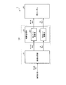
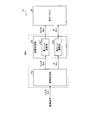
- FIG. 1 is a block diagram showing an example of the configuration of the display device according to the first embodiment.
- FIG. 2 is a block diagram showing an example of the configuration of the signal processing unit according to the first embodiment.
- FIG. 3 is a diagram showing an example of a gradation processing process in the first bit calculation unit according to the first embodiment.
- FIG. 4 is a diagram showing an example of a gradation processing process in the second bit calculation unit according to the first embodiment.
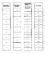
- FIG. 5 is a diagram showing display gradation values visually recognized on the display panel of the first embodiment.
- FIG. 6 is a diagram schematically showing the relationship between the gradation of each part and the display gradation value visually recognized on the display panel in the display device according to the first exemplary embodiment.
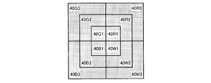
- FIG. 7 is a diagram showing an example of the pixel configuration of the display panel according to the first embodiment.
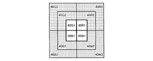
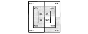
- FIG. 8A is a diagram showing the display pattern shown in A of FIGS. 5 and 6 for the R subpixel, the G subpixel, the B subpixel, and the W subpixel.
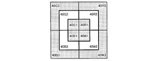
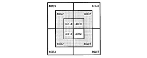
- FIG. 8B is a diagram showing display patterns shown in B of FIGS. 5 and 6 for the R subpixel, the G subpixel, the B subpixel, and the W subpixel.
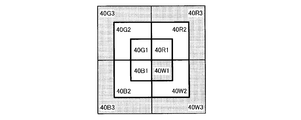
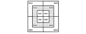
- FIG. 8C is a diagram showing the display pattern shown in C of FIGS. 5 and 6 for the R subpixel, the G subpixel, the B subpixel, and the W subpixel.
- FIG. 9 is a block diagram showing an example of the configuration of the signal processing unit according to the modified example of the first embodiment.
- FIG. 9 is a block diagram showing an example of the configuration of the signal processing unit according to the modified example of the first embodiment.
- FIG. 10 is a block diagram showing an example of the configuration of the signal processing unit according to the second embodiment.
- FIG. 11 is a diagram showing an example of the process of gradation processing in the first bit calculation unit according to the second embodiment.
- FIG. 12 is a diagram showing an example of the process of gradation processing in the second bit calculation unit according to the second embodiment.
- FIG. 13 is a diagram showing display gradation values visually recognized on the display panel of the second embodiment.
- FIG. 14 is a diagram schematically showing the relationship between the gradation of each part and the display gradation value visually recognized on the display panel in the display device according to the second exemplary embodiment.
- FIG. 15 is a diagram showing an example of the pixel configuration of the display panel according to the second embodiment.
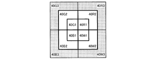
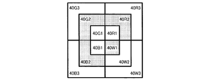
- FIG. 16A is a diagram showing an example of the display pattern shown in A of FIGS. 13 and 14 of the R sub-pixel, the G sub-pixel, the B sub-pixel, and the W sub-pixel.
- FIG. 16B is a diagram showing an example of the display pattern shown in B of FIGS. 13 and 14 of the R sub-pixel, the G sub-pixel, the B sub-pixel, and the W sub-pixel.
- FIG. 16C is a diagram showing an example of the display pattern shown in C of FIGS. 13 and 14 of the R sub-pixel, the G sub-pixel, the B sub-pixel, and the W sub-pixel.
- FIG. 16D is a diagram showing an example of the display pattern shown in D of FIGS.
- FIG. 16E is a diagram showing an example of the display pattern shown in E of FIGS. 13 and 14 of the R sub-pixel, the G sub-pixel, the B sub-pixel, and the W sub-pixel.
- FIG. 16F is a diagram showing an example of the display pattern shown in F of FIGS. 13 and 14 of the R sub-pixel, the G sub-pixel, the B sub-pixel, and the W sub-pixel.
- FIG. 16G is a diagram showing an example of the display pattern shown in G of FIGS. 13 and 14 for the R subpixel, the G subpixel, the B subpixel, and the W subpixel.
- FIG. 16H is a diagram showing an example of the display pattern shown in H of FIGS. 13 and 14 for the R subpixel, the G subpixel, the B subpixel, and the W subpixel.
- FIG. 17 is a block diagram showing an example of the configuration of the signal processing unit according to the third embodiment.
- FIG. 18 is a diagram showing an example of a gradation processing process in the first bit calculation unit according to the third embodiment.
- FIG. 19 is a diagram showing an example of a gradation processing process in the second bit calculation unit according to the third embodiment.
- FIG. 20 is a diagram showing display gradation values visually recognized on the display panel of the third embodiment.
- FIG. 21 is a diagram schematically showing the relationship between the gradation of each part and the display gradation value visually recognized on the display panel in the display device according to the third embodiment.
- FIG. 22 is a diagram showing an example of the pixel configuration of the display panel according to the third embodiment.
- FIG. 23A is a diagram showing an example of the display pattern shown in A of FIGS. 20 and 21 for the R subpixel, the G subpixel, the B subpixel, and the W subpixel.
- FIG. 23B is a diagram showing an example of the display patterns shown in FIGS. 20 and 21 of the R sub-pixel, the G sub-pixel, the B sub-pixel, and the W sub-pixel.
- FIG. 23C is a diagram showing an example of the display patterns shown in FIGS.
- FIG. 23D is a diagram showing an example of the display patterns shown in FIGS. 20 and 21 of the R sub-pixel, the G sub-pixel, the B sub-pixel, and the W sub-pixel.
- FIG. 23E is a diagram showing an example of the display pattern shown in E of FIGS. 20 and 21 of the R sub-pixel, the G sub-pixel, the B sub-pixel, and the W sub-pixel.
- FIG. 23F is a diagram showing an example of the display pattern shown in F of FIGS. 20 and 21 of the R sub-pixel, the G sub-pixel, the B sub-pixel, and the W sub-pixel.
- FIG. 23G is a diagram showing an example of the display pattern shown in G of FIGS. 20 and 21 of the R sub-pixel, the G sub-pixel, the B sub-pixel, and the W sub-pixel.
- FIG. 23H is a diagram showing an example of the display pattern shown in H of FIGS. 20 and 21 of the R sub-pixel, the G sub-pixel, the B sub-pixel, and the W sub-pixel.
- FIG. 23I is a diagram showing an example of the display patterns shown in FIGS. 20 and 21 of the R sub-pixel, the G sub-pixel, the B sub-pixel, and the W sub-pixel.
- FIG. 23J is a diagram showing an example of the display pattern shown in J of FIGS.
- FIG. 23K is a diagram showing an example of the display pattern shown in K of FIGS. 20 and 21 of the R sub-pixel, the G sub-pixel, the B sub-pixel, and the W sub-pixel.
- FIG. 23L is a diagram showing an example of the display pattern shown in L of FIGS. 20 and 21 of the R sub-pixel, the G sub-pixel, the B sub-pixel, and the W sub-pixel.
- FIG. 23M is a diagram showing an example of the display pattern shown in M of FIGS. 20 and 21 for the R subpixel, the G subpixel, the B subpixel, and the W subpixel.
- FIG. 23N is a diagram showing an example of the display pattern shown in N of FIGS. 20 and 21 of the R sub-pixel, the G sub-pixel, the B sub-pixel, and the W sub-pixel.
- FIG. 23O is a diagram showing an example of the display pattern shown in O of FIGS. 20 and 21 of the R sub-pixel, the G sub-pixel, the B sub-pixel, and the W sub-pixel.
- FIG. 24 is a block diagram showing an example of the configuration of the signal processing unit according to the fourth embodiment.
- FIG. 25 is a diagram showing an example of a gradation processing process in the first bit calculation unit according to the fourth embodiment.
- FIG. 26 is a diagram showing an example of a gradation processing process in the second bit calculation unit according to the fourth embodiment.
- FIG. 27 is a diagram showing display gradation values visually recognized on the display panel of the fourth embodiment.
- FIG. 28 is a diagram schematically showing the relationship between the gradation of each part and the display gradation value visually recognized on the display panel in the display device according to the fourth embodiment.
- FIG. 29A is a diagram showing an example of the display pattern shown in A of FIGS. 27 and 28 of the R sub-pixel, the G sub-pixel, the B sub-pixel, and the W sub-pixel.
- FIG. 29B is a diagram showing an example of the display pattern shown in B of FIGS. 27 and 28 of the R sub-pixel, the G sub-pixel, the B sub-pixel, and the W sub-pixel.
- FIG. 29C is a diagram showing an example of the display pattern shown in C of FIGS.
- FIG. 29D is a diagram showing an example of the display pattern shown in D of FIGS. 27 and 28 of the R sub-pixel, the G sub-pixel, the B sub-pixel, and the W sub-pixel.
- FIG. 29E is a diagram showing an example of the display pattern shown in E of FIGS. 27 and 28 of the R sub-pixel, the G sub-pixel, the B sub-pixel, and the W sub-pixel.
- FIG. 29F is a diagram showing an example of the display pattern shown in F of FIGS. 27 and 28 of the R sub-pixel, the G sub-pixel, the B sub-pixel, and the W sub-pixel.
- FIG. 29G is a diagram showing an example of the display pattern shown in G of FIGS. 27 and 28 of the R sub-pixel, the G sub-pixel, the B sub-pixel, and the W sub-pixel.
- FIG. 29H is a diagram showing an example of the display pattern shown in H of FIGS. 27 and 28 for the R subpixel, the G subpixel, the B subpixel, and the W subpixel.
- FIG. 29I is a diagram showing an example of the display pattern shown in I of FIGS. 27 and 28 of the R sub-pixel, the G sub-pixel, the B sub-pixel, and the W sub-pixel.
- FIG. 29J is a diagram showing an example of the display pattern shown in J of FIGS.
- FIG. 29K is a diagram showing an example of the display pattern shown in K of FIGS. 27 and 28 of the R sub-pixel, the G sub-pixel, the B sub-pixel, and the W sub-pixel.
- FIG. 29L is a diagram showing an example of the display pattern shown in L of FIGS. 27 and 28 of the R sub-pixel, the G sub-pixel, the B sub-pixel, and the W sub-pixel.
- FIG. 29M is a diagram showing an example of the display pattern shown in M of FIGS. 27 and 28 of the R sub-pixel, the G sub-pixel, the B sub-pixel, and the W sub-pixel.
- FIG. 29N is a diagram showing an example of the display pattern shown in N of FIGS. 27 and 28 of the R sub-pixel, the G sub-pixel, the B sub-pixel, and the W sub-pixel.
- FIG. 29O is a diagram showing an example of the display pattern shown in O of FIGS. 27 and 28 of the R sub-pixel, the G sub-pixel, the B sub-pixel, and the W sub-pixel.
- FIG. 29P is a diagram showing an example of the display pattern shown in P of FIGS. 27 and 28 of the R sub-pixel, the G sub-pixel, the B sub-pixel, and the W sub-pixel.
- FIG. 29Q is a diagram showing an example of the display patterns shown in Q of FIGS.
- FIG. 29R is a diagram showing an example of the display pattern of R subpixel, G subpixel, B subpixel, and W subpixel shown in R of FIGS. 27 and 28.
- FIG. 29S is a diagram showing an example of the display pattern shown in S of FIGS. 27 and 28 of the R sub-pixel, the G sub-pixel, the B sub-pixel, and the W sub-pixel.
- FIG. 29T is a diagram showing an example of the display pattern shown in T of FIGS. 27 and 28 of the R sub-pixel, the G sub-pixel, the B sub-pixel, and the W sub-pixel.
- FIG. 29U is a diagram showing an example of the display pattern of R sub-pixel, G sub-pixel, B sub-pixel, and W sub-pixel shown in U of FIGS. 27 and 28.
- FIG. 29V is a diagram showing an example of the display pattern shown in V of FIGS. 27 and 28 for the R subpixel, the G subpixel, the B subpixel, and the W subpixel.
- FIG. 1 is a block diagram showing an example of the configuration of the display device according to the first embodiment.
- the display device 1 of the first embodiment includes a signal processing unit 100 and a display panel 30.
- the display panel 30 has a display area 30a in which the pixels 40 are arranged in a two-dimensional matrix (matrix).
- the display panel 30 illustrates a liquid crystal display panel using a liquid crystal display element as a display element constituting the pixel 40.
- the display panel 30 may be an organic EL display panel using an organic light emitting diode (OLED) as a display element, an inorganic EL display using an inorganic light emitting diode (micro LED), or the like. ..
- OLED organic light emitting diode
- micro LED inorganic light emitting diode
- the present disclosure is not limited by the aspect of the display element forming the pixel 40.
- the pixel 40 has three primary color subpixels of R (red) subpixel (first pixel), G (green) subpixel (second pixel), and B (blue) subpixel (third pixel), and W (White) It is composed of a plurality of sub-pixels including a sub-pixel (fourth pixel). Each sub-pixel constituting the pixel 40 will be described later.
- the display panel 30 includes a signal output circuit 31 and a scanning circuit 32.
- the signal output circuit 31 is electrically connected to each sub-pixel included in each pixel 40 by a signal line DTL.
- the signal output circuit 31 sequentially outputs an output signal to each sub-pixel included in each pixel 40.
- the scanning circuit 32 is electrically connected to each sub-pixel included in each pixel 40 by a scanning line SCL.
- the scanning circuit 32 selects each sub-pixel included in each pixel 40 and controls on / off of a switching element (for example, a thin film transistor (TFT)) for controlling the operation of each sub-pixel.
- a switching element for example, a thin film transistor (TFT)
- the display panel 30 includes an R (red) subpixel (first pixel), a G (green) subpixel (second pixel), a B (blue) subpixel (third pixel), and a W (white) subpixel (first pixel).
- Each of the four pixels) has a display gradation of a predetermined number of bits.
- the display gradation of the display panel 30 is 256 gradations, that is, a gradation expression having an 8-bit depth is possible will be described, but the display gradation of the display panel 30 is limited to 256 gradations. is not.
- the display brightness of the R (red) sub-pixel (first pixel), the G (green) sub-pixel (second pixel), the B (blue) sub-pixel (third pixel), and the W (white) sub-pixel The ratio of the pixel (fourth pixel) to the display brightness is 1: 1. In other words, assuming that the brightness when displaying white in one pixel is "1", R (red) sub-pixel (first pixel), G (green) sub-pixel (second pixel), B (blue) The luminance of the sub-pixel (third pixel) and the luminance of the W (white) sub-pixel (fourth pixel) are both “0.5”.
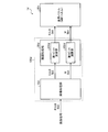
- FIG. 2 is a block diagram showing an example of the configuration of the signal processing unit according to the first embodiment.
- the signal processing unit 100 includes an image processing unit 10 and a gradation processing unit 20.
- An image signal including gradation data of three primary colors of R (red), G (green), and B (blue) is input to the signal processing unit 100 from the host IC 200 of the host system.
- each gradation data of the three primary colors R (red), G (green), and B (blue) of the image signal has an 8-bit depth per sub-pixel will be described, but each gradation of the image signal will be described.
- the data is not limited to 8-bit depth.
- the image processing unit 10 inputs R (red), G (green), and B (blue) image signals including the input R (red), G (green), and B (blue) color 8-bit depth gradation data. It is converted into an RGB signal (first signal) containing each gradation data of 9-bit depth of each color of blue) and a W signal (second signal) including gradation data of 9-bit depth of W (white).
- RGB signal first signal
- W signal second signal
- the present disclosure is not limited to the method of image conversion processing in the image processing unit 10.
- the image processing unit 10 converts the data for one bit of the fraction generated by the internal arithmetic processing such as expansion processing into R ( It is added as the least significant bit to each gradation data of (red), G (green), B (blue), and W (white). As a result, the image processing unit 10 outputs a 9-bit depth RGB signal (first signal) and a 9-bit depth W signal (second signal) with an increased bit depth.
- the gradation processing unit 20 includes a first bit calculation unit 201 and a second bit calculation unit 202.
- the first bit calculation unit 201 performs the first bit calculation processing described later on the RGB signal having a depth of 9 bits output from the image processing unit 10, generates an RGB signal having a depth of 8 bits, and outputs the signal.
- the second bit calculation unit 202 performs the second bit calculation processing described later on the 9-bit depth W signal output from the image processing unit 10, generates an 8-bit depth W signal, and outputs the W signal.
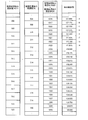
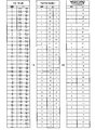
- FIG. 3 is a diagram showing an example of the gradation processing process in the first bit calculation unit according to the first embodiment.
- FIG. 4 is a diagram showing an example of a gradation processing process in the second bit calculation unit according to the first embodiment.
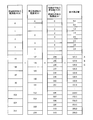
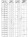
- FIG. 5 is a diagram showing display gradation values visually recognized on the display panel of the first embodiment.
- FIG. 6 is a diagram schematically showing the relationship between the gradation of each part and the display gradation value visually recognized on the display panel in the display device according to the first exemplary embodiment.
- each gradation data of R (red), G (green), and B (blue) included in the image signal input to the signal processing unit 100 is expanded by the image processing unit 10.
- the number of bits increases in the process of image processing such as.
- the 8-bit depth (256 gradations) R (red), G (green), and B (blue) gradation data input to the image processing unit 10 has a 9-bit depth (512 gradations).
- the RGB signal converted into each gradation data of 9-bit depth (512 gradations) is input to the first bit calculation unit 201 of the gradation processing unit 20.
- the W signal converted into gradation data having a depth of 9 bits (512 gradations) is input to the second bit calculation unit 202 of the gradation processing unit 20.
- the least significant bit of each gradation data of 9-bit depth is "0 bit” and the most significant bit is "8 bit”.
- the 0-bit values of the RGB signal gradation data and the W signal gradation data after image processing in the image processing unit 10 are "0" and "1". Either one can be taken.
- the first bit calculation unit 201 of the gradation processing unit 20 converts each gradation data of an RGB signal having a 9-bit depth (512 gradations) into an 8-bit depth (256 gradations). Specifically, as shown in FIG. 3, the first bit calculation unit 201 has the 0th bit (0 bit) of each gradation data of R (red), G (green), and B (blue) having a depth of 9 bits (512 gradations). The least significant bit) is rounded down to an 8-bit depth and output to the display panel 30.
- the second bit calculation unit 202 of the gradation processing unit 20 converts the gradation data of the W signal having a depth of 9 bits (512 gradations) into an 8-bit depth (256 gradations). Specifically, as shown in FIG. 4, the second bit computing unit 202 adds the data value “1” to the grayscale data of W (white) of 9-bit depth (512 grayscales), and then adds the data value of 0 bit ( The least significant bit) is rounded down to an 8-bit depth and output to the display panel 30.
- the RGB signal after gradation processing (first signal) ) And the gradation data of the W signal (second signal) have the same value and the value deviated by 1 from each other.
- the grayscale data of the RGB signal (first signal) and the grayscale data of the W signal (second signal) after the grayscale processing have values that deviate from each other by 1, the 8-bit depth, that is, 256.
- an intermediate value of each gradation value can be expressed. Specifically, since an intermediate value of 8-bit depth (256 gradations) can be expressed, an apparent floor visually recognized on the display panel 30 capable of 8-bit depth (256 gradations) gradation expression.
- the key can be set to 511 steps.
- the gradation value of each gradation data of R (red), G (green), and B (blue) after gradation processing is “127”, and W (white) after gradation processing.
- the gradation value of the gradation data of) is "127”
- the gradation values of R (red), G (green), and B (blue) after the gradation processing are "127” and W
- the apparent display gradation value of the image displayed on the display panel 30 capable of 8-bit depth (256 gradations) gradation display is “127.0” (A in FIGS. 5 and 6). reference).
- the gradation value of each gradation data of R (red), G (green), and B (blue) after gradation processing is “127”, and W after gradation processing is W.
- the gradation value of the (white) gradation data is “128”
- the gradation value of each of the R (red), G (green), and B (blue) gradation data after gradation processing is “127”.
- the gradation value "128" of the gradation data of W (white) is added, it becomes "255”.
- the apparent display gradation value of the image displayed on the display panel 30 capable of gradation expression of 8-bit depth (256 gradations) is “127.5” (B in FIGS. 5 and 6). reference).
- the gradation value of each gradation data of R (red), G (green), and B (blue) after gradation processing is “128”, and W after gradation processing is W.
- the gradation value of the (white) gradation data is “128”
- the gradation value of each of the R (red), G (green), and B (blue) gradation data after the gradation processing is “128”.
- the gradation value "128" of the gradation data of W (white) is added, it becomes "256”.
- the apparent display grayscale value of the image displayed on the display panel 30 capable of 8-bit depth (256 grayscale) gradation display is “128.0” (C in FIGS. 5 and 6). reference).
- the intermediate value of each gradation value can be expressed on the display panel 30 capable of expressing the gradation of 8-bit depth (256 gradations).
- the apparent gradation visually recognized on the display panel 30 can be set to 511 steps.
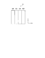
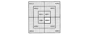
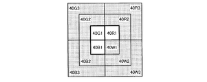
- FIG. 7 is a diagram showing an example of the pixel configuration of the display panel according to the first embodiment.
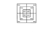
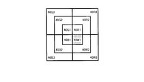
- a plurality of pixels 40 shown in FIG. 7 are arranged and arranged in the X direction and the Y direction in the display area of the display panel 30.
- the pixel 40 includes an R (red) sub-pixel 40R (first pixel), a G (green) sub-pixel 40G (second pixel), a B (blue) sub-pixel 40B (third pixel), and a W (white) sub-pixel. It has 40 W (fourth pixel).
- the display gradation of each sub-pixel 40R, 40G, 40B, 40W can be 256 gradations, that is, gradation expression with an 8-bit depth is possible.
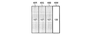
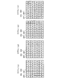
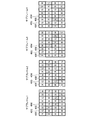
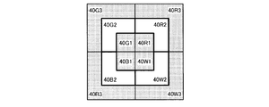
- FIG. 8A is a diagram showing the display patterns shown in A of FIGS. 5 and 6 of the R sub-pixel, the G sub-pixel, the B sub-pixel, and the W sub-pixel.
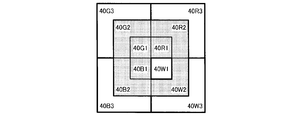
- FIG. 8B is a diagram showing display patterns shown in B of FIGS. 5 and 6 for the R subpixel, the G subpixel, the B subpixel, and the W subpixel.
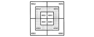
- FIG. 8C is a diagram showing the display pattern shown in C of FIGS. 5 and 6 for the R subpixel, the G subpixel, the B subpixel, and the W subpixel.
- the ratio of the display brightness of the R sub-pixel 40R, the G sub-pixel 40G, and the B sub-pixel 40B to the display brightness of the W sub-pixel 40W is 1: 1.
- the shaded sub-pixel display gradation is "127" and the white sub-pixel display gradation is "128".
- the display gradation "127" of the R sub-pixel 40R, the G sub-pixel 40G, and the B sub-pixel 40B and the display gradation "127" of the W sub-pixel 40W are added to obtain "254".
- the apparent display gradation value of the pixel 40 capable of expressing gradation with an 8-bit depth (256 gradations) is "127.0".
- the first bit calculation unit 201 of the gradation processing unit 20 cuts off the 0-bitth of each gradation data of the RGB signal having a depth of 9 bits (512 gradations) and has an 8-bit depth (256). And output to the display panel 30. Further, the second bit calculation unit 202 of the gradation processing unit 20 adds the data value "1" to the gradation data of the W signal having a depth of 9 bits (512 gradations), and then truncates the 0th bit to the depth of 8 bits. (256 gradations) and output to the display panel 30. As a result, the number of display gradations is 256, that is, the apparent gradation visually recognized on the display panel 30 capable of expressing gradations having an 8-bit depth (256 gradations) can be set to 511 steps.
- the 0th bit is truncated to an 8-bit depth. (256 gradations)
- the 0th bit of the gradation data of the W signal having a depth of 9 bits (512 gradations) is truncated to an 8-bit depth (256 gradations). May be adopted.
- FIG. 9 is a block diagram showing an example of the configuration of the signal processing unit according to the modified example of the first embodiment.
- each gradation data of three primary colors of R (red), G (green), and B (blue) of the image signal input to the signal processing unit 100a of the display device 1a is 1.
- An example in which the depth is 9 bits per sub-pixel will be described.
- the image conversion process in the image processing unit 10a is not affected by the fraction generated by the internal calculation process such as the decompression process. That is, in the modified example of the first embodiment shown in FIG. 9, when each gradation data of the image signal has the same value, each gradation data of the 9-bit depth RGB signal (first signal) output from the image processing unit 10a. And the grayscale data of the 9-bit depth W signal (second signal) have the same value. In this case, if each gradation data of the image signal is increased by one step, each gradation data and 9-bit depth of the RGB signal (first signal) of the 9-bit depth after the gradation processing output from the gradation processing unit 20.
- the grayscale data of the W signal (second signal) is alternately increased and the grayscale data of the image signal is decreased by one step, the 9-bit depth after the grayscale processing output from the grayscale processing unit 20.
- Each gradation data of the RGB signal (first signal) and the gradation data of the W signal (second signal) having a depth of 9 bits are alternately reduced.
- each gradation data of the three primary colors R (red), G (green), and B (blue) of the image signal input to the signal processing unit 100a of the display device 1a has a depth of 9 bits per sub-pixel.
- each gradation data of the three primary colors R (red), G (green), and B (blue) of the image signal has a depth of 10 bits or more per sub-pixel. ..
- the display devices 1 and 1a according to the first embodiment and the modified examples of the first embodiment have R (red) sub-pixel 40R (first pixel) and G (green) sub-pixel 40G (second pixel).
- a display panel 30 composed of a plurality of pixels 40 including W (white) sub-pixels 40W (fourth pixel) in addition to each sub-pixel of the three primary colors of B (blue) sub-pixels 40B (third pixel).
- An image signal containing R (red), G (green), and B (blue) gradation data is used as an RGB signal (first signal) containing R (red), G (green), and B (blue) gradation data.
- a signal processing unit 100 that converts and outputs a W signal (second signal) including W (white) gradation data.
- the signal processing unit 100 when each gradation data of the image signal has the same value, each gradation data of the RGB signal (first signal) and the gradation data of the W signal (second signal) have the same value. The case and the case where the values are shifted from each other by 1 are mixed.
- the signal processing unit 100 converts the gradation data of the RGB signal (first signal) and the W signal (second signal) of the first bit depth (9 bit depth) into the second bit depth (8) smaller than the first bit depth.
- the gradation processing unit 20 for converting into a bit depth) is provided.
- the gradation processing unit 20 cuts off the 0th bit of each gradation data of the RGB signal (first signal) having the first bit depth (9 bit depth) to obtain the second bit depth (8 bit depth). After adding 1 to the grayscale data of the W signal (second signal) of 1-bit depth (9-bit depth), the 0th bit is discarded to obtain the second bit depth (8-bit depth).
- the gradation processing unit 20 adds 1 to each gradation data of the RGB signal (first signal) having the first bit depth (9-bit depth), and then truncates the 0-bit depth to the second bit depth (8-bit depth). ), The 0-bit th of the gradation data of the W signal (second signal) of the first bit depth (9 bit depth) is truncated to obtain the second bit depth (8 bit depth).
- the display panel 30 capable of expressing the gradation of the second bit depth (8 bit depth, that is, 256 gradations)
- an intermediate value of each gradation value can be expressed and visually recognized on the display panel 30.
- the apparent gradation can be increased. In other words, it is possible to express a gradation higher than the display gradation of the display panel 30.
- the display brightness of the R (red) sub-pixel (first pixel), the G (green) sub-pixel (second pixel), and the B (blue) sub-pixel (third pixel) and W The case where the ratio of the (white) sub-pixel (fourth pixel) to the display brightness is 1: 1 has been described, but the R (red) sub-pixel (first pixel) and the G (green) sub-pixel (second pixel) have been described. ),
- the ratio of the display brightness of the B (blue) sub-pixel (third pixel) to the display brightness of the W (white) sub-pixel (fourth pixel) is not limited to this, for example, the R (red) sub-pixel.
- the ratio may be unequal such as 1:0.5. Even in this case, the display brightness is increased by increasing the gradation data of the image signal, and the display brightness is decreased by decreasing the gradation data of the image signal. That is, the inversion phenomenon of the display luminance with respect to the change of the image signal does not occur.
- FIG. 10 is a block diagram showing an example of the configuration of the signal processing unit according to the second embodiment.
- the display device 1b according to the present embodiment is configured to perform a frame rate control (FRC) process in which an image of one frame is time-divided into a plurality of subframes for display.
- FRC frame rate control
- the display device 1b according to the second embodiment includes the FRC control unit 50 at the subsequent stage of the gradation processing unit 20b.
- a known method can be used for the frame rate control process in the FRC control unit 50.
- the present disclosure is not limited to the method of the frame rate control processing in the FRC control unit 50.
- the FRC control unit 50 displays an image of one frame by time division into four subframes, for example. It is possible to extend the gradation expression for 2 bits. That is, as shown in FIG. 10, when the display gradation of the display panel 30b is 256 gradations, that is, when the input signal that can be displayed on the display panel 30b is 8 bit depth, the frame rate control by the FRC control unit 50 is performed. By processing, gradation expression with a depth of 10 bits (2048 gradations) is possible.
- the image processing unit 10b transmits the input image signals including the gradation data of each color of R (red), G (green), and B (blue) at a depth of 8 bits to R (red), G (green), and B ( It is converted into an RGB signal (first signal) containing each gradation data of 11-bit depth of each color of blue) and a W signal (second signal) including gradation data of 11-bit depth of W (white).
- the image processing unit 10b uses R (red), G (green), B (blue), and W (white) for data equivalent to 3 bits generated by internal arithmetic processing such as decompression processing. Is added as lower 3 bits to each gradation data. As a result, the image processing unit 10b outputs an RGB signal (first signal) having an increased bit depth of 11 bits and a W signal (second signal) having an increased bit depth.
- FIG. 11 is a diagram showing an example of the process of gradation processing in the first bit calculation unit according to the second embodiment.
- FIG. 12 is a diagram showing an example of a gradation processing process in the second bit calculation unit according to the second embodiment.
- FIG. 13 is a diagram showing display gradation values visually recognized on the display panel of the second embodiment.
- FIG. 14 is a diagram schematically showing the relationship between the gradation of each part and the display gradation value visually recognized on the display panel in the display device according to the second exemplary embodiment.
- each gradation data of R (red), G (green), and B (blue) included in the image signal input to the signal processing unit 100b is expanded by the image processing unit 10b.
- the number of bits increases in the process of image processing such as.
- the 8-bit depth (256 gradations) R (red), G (green), and B (blue) gradation data input to the image processing unit 10b has an 11-bit depth (2048 gradations).
- the RGB signal converted into each gradation data of 11-bit depth (2048 gradations) is input to the first bit calculation unit 201b of the gradation processing unit 20b.
- the W signal converted into the gradation data of 11-bit depth (2048 gradations) is input to the second bit calculation unit 202b of the gradation processing unit 20b.
- the least significant bit of each gradation data of 11-bit depth is "0 bit”
- the most significant bit is "10 bit”.
- the values of the second bit, the first bit, and the 0 bit of the RGB signal gradation data and the W signal gradation data after image processing in the image processing unit 10b are "000". , “001”, “010”, “011”, “100”, “101”, “110”, “111”.
- the first bit calculation unit 201b of the gradation processing unit 20b converts each gradation data of an RGB signal having an 11-bit depth (2048 gradations) into a 10-bit depth (1024 gradations). Specifically, as shown in FIG. 11, the first bit calculation unit 201b is the 0th bit (0 bit) of each gradation data of R (red), G (green), and B (blue) having an 11-bit depth (2048 gradations). The least significant bit) is truncated to a depth of 10 bits (1024 gradations), and the data is output to the display panel 30b.
- the second bit calculation unit 202b of the gradation processing unit 20b converts the gradation data of the W signal having an 11-bit depth (2048 gradation) into a 10-bit depth (1024 gradation). Specifically, as shown in FIG. 12, the second bit calculation unit 202b adds the data value “1” to the W (white) gradation data having an 11-bit depth (2048 gradations), and then the 0th bit ( The least significant bit) is truncated to a depth of 10 bits (1024 gradations), and the data is output to the display panel 30b.
- the gradation processing of the second bit calculation unit 202b of the gradation processing unit 20b In, the data value "1" is not added. Thereby, bit overflow can be prevented.
- the display panel 30b capable of gradation expression is configured to enable gradation expression of 10-bit depth (1024 gradations) by the frame rate control processing in the FRC control unit 50 described above. Can be expressed.
- the intermediate value of 10-bit depth (1024 gradations) can be expressed, the apparent floor visually recognized on the display panel 30b capable of expressing gradation of 8-bit depth (256 gradations).
- the key can be 2047 steps.
- the gradation value of each gradation data of R (red), G (green), and B (blue) after gradation processing is "508", and W (white) after gradation processing.
- the gradation value of the gradation data of) is "508”
- the gradation values of R (red), G (green), and B (blue) after the gradation processing are "508” and W (
- the gradation value "508" of the gradation data of white) is added, it becomes “1016".
- the apparent display gradation value of the image displayed by the signal after the frame rate control processing by the FRC control unit 50 described above. Is “127,000” (see A in FIGS. 13 and 14).
- the gradation value of each gradation data of R (red), G (green), and B (blue) after the gradation processing is "508", and W after the gradation processing.
- the gradation value of the gradation data of (white) is "509”
- the gradation value of each gradation data of R (red), G (green), and B (blue) after the gradation processing is "508”.
- Addition with the gradation value “509” of the gradation data of W (white) gives “1017”.
- the gradation value of each gradation data of R (red), G (green), and B (blue) after the gradation processing is "509", and W after the gradation processing.
- the gradation value of the gradation data of (white) is "509”
- the gradation value of each gradation data of R (red), G (green), and B (blue) after the gradation processing is "509”.
- the gradation value "509" of the gradation data of W (white) is added, it becomes "1018".
- the gradation value of each gradation data of R (red), G (green), and B (blue) after the gradation processing is "509", and W after the gradation processing.
- the gradation value of the gradation data of (white) is "510”
- the gradation value of each gradation data of R (red), G (green), and B (blue) after the gradation processing is "509”.
- Addition with the gradation value "510" of the gradation data of W (white) gives "1019".
- the gradation value of each gradation data of R (red), G (green), and B (blue) after the gradation processing is "510", and W after the gradation processing.
- the gradation value of the gradation data of (white) is "510”
- the gradation value of each gradation data of R (red), G (green), and B (blue) after the gradation processing is "510”.
- Addition with the gradation value “510” of the W (white) gradation data results in “1020”.
- the gradation value of each gradation data of R (red), G (green), and B (blue) after the gradation processing is "510", and W after the gradation processing.
- the gradation value of the (white) gradation data is “511”
- the gradation value of each of the R (red), G (green) and B (blue) gradation data after the gradation processing is “510”.
- the gradation value "511" of the gradation data of W (white) is added, it becomes "1021".
- the gradation value of each gradation data of R (red), G (green), and B (blue) after the gradation processing is "511", and W after the gradation processing.
- the gradation value of the gradation data of (white) is "511”
- the gradation value of each gradation data of R (red), G (green), and B (blue) after the gradation processing is "511”.
- Addition with the gradation value “511” of the gradation data of W (white) gives “1022”.
- the gradation value of each gradation data of R (red), G (green), and B (blue) after the gradation processing is "511", and W after the gradation processing.
- the gradation value of the gradation data of (white) is "512”
- the gradation value of each gradation data of R (red), G (green), and B (blue) after the gradation processing is "511”.
- Addition with the gradation value “512” of the gradation data of W (white) gives “1023”.
- the apparent display gradation value of the image displayed by the signal after the frame rate control processing by the FRC control unit 50 described above. Is "127.875" (see H in FIGS. 13 and 14).
- the signal after the frame rate control processing in the FRC control unit 50 described above causes the 10 bit depth (1024th floor). It is possible to express the intermediate value of each gradation value of the (tone). As a result, the apparent gradation visually recognized on the display panel 30a capable of expressing gradation with an 8-bit depth (256 gradations) can be set to 2047 steps.
- FIG. 15 is a diagram showing an example of the pixel configuration of the display panel according to the second embodiment.
- the display panel 30b has a plurality of R (red) sub-pixels 40R (first pixel), G (green) sub-pixels 40G (second pixel), and B (blue) sub-pixels 40B (third pixel).
- the pixel group 41 having a plurality of W (white) sub-pixels 40W (fourth pixel) is displayed as one group.
- the display gradation of each sub-pixel 40R, 40G, 40B, 40W is 256 gradations, that is, gradation expression with an 8-bit depth is possible. In the example shown in FIG.
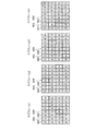
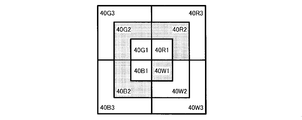
- FIG. 16A is a diagram showing an example of the display pattern shown in A of FIGS. 13 and 14 of the R sub-pixel, the G sub-pixel, the B sub-pixel, and the W sub-pixel.
- FIG. 16B is a diagram showing an example of the display pattern shown in B of FIGS. 13 and 14 of the R sub-pixel, the G sub-pixel, the B sub-pixel, and the W sub-pixel.
- FIG. 16C is a diagram showing an example of the display pattern shown in C of FIGS. 13 and 14 of the R sub-pixel, the G sub-pixel, the B sub-pixel, and the W sub-pixel.
- FIG. 16D is a diagram showing an example of the display pattern shown in D of FIGS.
- FIG. 16E is a diagram showing an example of the display pattern shown in E of FIGS. 13 and 14 of the R sub-pixel, the G sub-pixel, the B sub-pixel, and the W sub-pixel.
- FIG. 16F is a diagram showing an example of the display pattern shown in F of FIGS. 13 and 14 of the R sub-pixel, the G sub-pixel, the B sub-pixel, and the W sub-pixel.
- FIG. 16G is a diagram showing an example of the display pattern shown in G of FIGS. 13 and 14 for the R subpixel, the G subpixel, the B subpixel, and the W subpixel.
- FIGS. 16H is a diagram showing an example of the display pattern shown in H of FIGS. 13 and 14 for the R subpixel, the G subpixel, the B subpixel, and the W subpixel.
- a set of R sub-pixels 40R, a G sub-pixel 40G, a B sub-pixel 40B, and one W sub-pixel 40W constitute a pixel 40, and a set of R sub-pixels.
- the ratio of the display brightness of the 40R, G sub-pixel 40G, and B sub-pixel 40B to the display brightness of one W sub-pixel 40W is 1: 1.
- each display pattern shown in FIGS. 16A to 16H is an example, and is not limited to the example shown in FIGS. 16A to 16H.
- the image of one frame is time-divisioned into four subframes and displayed.
- the FRC control unit 50 displays the subframe 1, the subframe 2, the subframe 3, and the subframe 4 shown in FIGS. 16A to 16H in this order with respect to the pixel group 41 shown in FIG.
- 10-bit depth (1024 gradations) gradation can be expressed by the frame rate control process by the FRC controller 50.
- the shaded sub-pixel display gradation is "127" and the white sub-pixel display gradation is "128".
- the apparent display gradation value of the pixel 40 capable of expressing gradation with an 8-bit depth (256 gradations) is "127.000".
- the apparent display gradation value of the pixel 40 capable of expressing gradation with an 8-bit depth (256 gradations) is "127.125".
- the apparent display gradation value of the pixel 40 capable of expressing gradation with an 8-bit depth (256 gradations) is "127.250".
- four W sub-pixel 40W display gradation "128 x 4" are added.
- the apparent display gradation value of the pixel 40 capable of expressing gradation with an 8-bit depth (256 gradations) is "127.375".
- B sub-pixel 40B display gradation "128 x 4", four W sub-pixel 40W display gradation "127 x 4", and four W sub-pixel 40W display gradation "128 x 4" are added.
- the display gradation per pixel 40 constituting the pixel group 41 becomes "2040/8 255.000".
- the apparent display gradation value of the pixel 40 capable of expressing gradation with an 8-bit depth (256 gradations) is "127.500".
- B sub-pixel 40B display gradation "128x4", two W sub-pixel 40W display gradation "127x2”, and six W sub-pixel 40W display gradation "128x6" are added.
- the apparent display gradation value of the pixel 40 capable of expressing gradation with an 8-bit depth (256 gradations) is "127.675".
- B sub-pixel 40B display gradation "128 x 6"
- six W sub-pixel 40W display gradation "128 x 6" are added.
- the apparent display gradation value of the pixel 40 capable of expressing gradation with an 8-bit depth (256 gradations) is "127.750".
- the display gradation "128 x 6" of the B sub-pixel 40B and the display gradation "128 x 8" of the eight W sub-pixels 40W are added to obtain "2046", which is per 40 pixels constituting the pixel group 41.
- the apparent display gradation value of the pixel 40 capable of expressing gradation with an 8-bit depth (256 gradations) is "127.875".
- the first bit calculation unit 201b of the gradation processing unit 20b cuts off the 0th bit of each gradation data of the RGB signal having an 11-bit depth (2048 gradation) to a depth of 10 bits (1024).
- the second bit calculation unit 202b of the gradation processing unit 20b adds the data value "1" to the gradation data of the W signal having an 11-bit depth (2048 gradation), and then cuts off the 0th bit.
- the depth is 10 bits (1024 gradations).
- the FRC control unit 50 performs frame rate control processing on RGB signals and W signals having a depth of 10 bits (1024 gradations) and outputs them to the display panel 30b.
- the apparent gradation visually recognized on the display panel 30b capable of expressing gradation having a display gradation number of 256, that is, an 8-bit depth (256 gradations) can be set to 2047 steps.
- the 0th bit is truncated to a 10-bit depth. (1024 gradations)
- the 0th bit of the gradation data of the W signal having an 11-bit depth (2048 gradations) is truncated to 10-bit depth (1024 gradations). It may be in the mode of.
- the display device 1b further includes the FRC control unit 50 that time-divides one frame image into a plurality of sub-frames and supplies the sub-frame to the display panel 30b.
- the FRC control unit 50 displays on the display panel 30b in a plurality of display patterns according to each gradation data of the RGB signal (first signal) and the gradation data of the W signal (second signal).
- the signal after the frame rate control processing in the FRC controller 50 causes 10 bit depth (1024 gradations). It is possible to express an intermediate value of each gradation value of, and it is possible to increase the apparent gradation visually recognized on the display panel 30b as compared with the first embodiment.
- FIG. 17 is a block diagram showing an example of the configuration of the signal processing unit according to the third embodiment.
- the display panel 30c has a memory capable of storing binary data (logical value “1” or logical value “0”) in each pixel.
- MIP Memory In Pixel
- the sub-pixel (fourth pixel) is composed of a plurality of segments having the same area ratio, and the combination of the on state and the off state of each segment realizes the display of a plurality of gradations in each sub-pixel.
- This is a so-called area gradation method configuration.
- the display gradation of the display panel 30c is 8 gradations, that is, the gradation expression of 3 bit depth is possible will be described, but the display gradation of the display panel 30c is limited to 8 gradations. is not.
- the display panel 30c includes, for example, R subpixels, G subpixels, B subpixels, and W subpixels.
- R subpixels for example, R subpixels, G subpixels, B subpixels, and W subpixels.
- the pixels are composed of three segments each having an area ratio of 1: 2: 4, and the number of display gradations of the pixels is 8, that is, the bit depth is 3 bits.
- the bit depth of the display gradation of each subpixel is not limited to 8 bits.
- the image processing unit 10c converts the input image signal including the gradation data of each color of R (red), G (green), and B (blue) at an 8-bit depth into R (red), G (green), and B ( It is converted into an RGB signal (first signal) containing each gradation data of each color with a depth of 4 bits (blue) and a W signal (second signal) containing gradation data with a depth of 4 bits of W (white).
- the image processing unit 10c sets the lower bits of each gradation data of the RGB signal (first signal) and the gradation data of the W signal (second signal) whose bit depth is increased by internal arithmetic processing such as expansion processing. Outputs the truncated gradation data of the upper 4 bit depth.
- FIG. 18 is a diagram showing an example of a process of gradation processing in the first bit arithmetic unit according to the third embodiment.
- FIG. 19 is a diagram showing an example of a gradation processing process in the second bit calculation unit according to the third embodiment.
- FIG. 20 is a diagram showing display gradation values visually recognized on the display panel of the third embodiment.
- FIG. 21 is a diagram schematically showing the relationship between the gradation of each part and the display gradation value visually recognized on the display panel in the display device according to the third embodiment.
- 8-bit depth (256 tones) of R (red), G (green), and B (blue) included in the image signal input to the signal processing unit 100c Is an RGB signal including gradation data of R (red), G (green), and B (blue) 4 bit depth (16 gradations), and W (white) 4 bit depth (in the image processing unit 10c). It is converted into a W signal containing gradation data (16 gradations).
- the RGB signal converted into each gradation data having a 4-bit depth (16 gradations) is input to the first bit calculation unit 201c of the gradation processing unit 20c.
- the W signal converted into gradation data having a depth of 4 bits (16 gradations) is input to the second bit calculation unit 202c of the gradation processing unit 20c.
- a W signal having an 8-bit depth (256 gradations) is obtained by truncating the 3rd bit or less of each gradation data of an 8-bit depth (256 gradations) RGB signal to a 4-bit depth (16 gradations).
- 3 shows an example in which the third and lower bits of the gradation data are truncated to form a 4-bit depth (16 gradations).
- the first bit calculation unit 201c of the gradation processing unit 20c converts each gradation data of an RGB signal having a 4-bit depth (16 gradations) into a 3-bit depth (8 gradations). Specifically, as shown in FIG. 18, the first bit operation unit 201c sets the 0-bit (of each gradation data of R (red), G (green), and B (blue) of 4-bit depth (16 gradations) ( The least significant bit) is truncated to a depth of 3 bits (8 gradations), which is output to the display panel 30c.
- the second bit calculation unit 202c of the gradation processing unit 20c converts the gradation data of the W signal having a depth of 4 bits (16 gradations) into a depth of 3 bits (8 gradations). Specifically, as shown in FIG. 19, the second bit operation unit 202c adds the data value “1” to the W (white) gradation data of 4 bit depth (16 gradations), and then adds 0 bit ( The least significant bit) is truncated to a depth of 3 bits (8 gradations), and the data is output to the display panel 30c.
- the gradation data “1111” of the 4-bit depth (16 gradations) W signal output from the image processing unit 10c is processed by the second bit operation unit 202c of the gradation processing unit 20c. , The data value "1" is not added. Thereby, bit overflow can be prevented.
- the depth is 3 bits, that is, 8
- an intermediate value of each gradation value can be expressed. Specifically, since the intermediate value of the 3-bit depth (8 gradations) can be expressed, the apparent floor visually recognized on the display panel 30c capable of expressing the gradation of the 3-bit depth (8 gradations).
- the key can be set to 15 levels.
- the gradation value of each gradation data of R (red), G (green), and B (blue) after gradation processing is “0”, and W (white) after gradation processing.
- the gradation value of the gradation data of) is "0”
- the gradation values of R (red), G (green), and B (blue) after the gradation processing are "0” and W
- the apparent display gradation value of the image displayed on the display panel 30c capable of expressing gradation with a depth of 3 bits (8 gradations) is "0.0" (A in FIGS. 20 and 21). reference).
- the gradation value of each gradation data of R (red), G (green), and B (blue) after the gradation processing is “0”, and W after the gradation processing.
- the gradation value of the (white) gradation data is “1”
- the gradation value of each of the R (red), G (green), and B (blue) gradation data after gradation processing is “0”.
- the gradation value "1" of the gradation data of W (white) is added, it becomes “1”.
- the apparent display gradation value of the image displayed on the display panel 30c capable of expressing gradation with a depth of 3 bits (8 gradations) is "0.5" (B in FIGS. 20 and 21). reference).
- the gradation value of each gradation data of R (red), G (green), and B (blue) after the gradation processing is “1", and W after the gradation processing.
- the gradation value of the (white) gradation data is “1”
- the gradation value of each of the R (red), G (green), and B (blue) gradation data after the gradation processing is “1”.
- the gradation value "1" of the gradation data of W (white) is added, it becomes “2”.
- the apparent display gradation value of the image displayed on the display panel 30c capable of expressing gradation with a depth of 3 bits (8 gradations) is "1.0" (C in FIGS. 20 and 21). reference).
- the gradation value of each gradation data of R (red), G (green), and B (blue) after the gradation processing is "1", and W after the gradation processing.
- the gradation value of the (white) gradation data is “2”
- the gradation value of each of the R (red), G (green), and B (blue) gradation data after gradation processing is “1”.
- the gradation value "2" of the gradation data of W (white) is added, it becomes “3”.
- the apparent display gradation value of the image displayed on the display panel 30c capable of expressing gradation with a depth of 3 bits (8 gradations) is "1.5" (D in FIGS. 20 and 21). reference).
- the gradation value of each gradation data of R (red), G (green), and B (blue) after the gradation processing is "2", and W after the gradation processing.
- the gradation value of the (white) gradation data is “2”
- the gradation value of each of the R (red), G (green), and B (blue) gradation data after the gradation processing is “2”.
- the gradation value "2" of the gradation data of W (white) is added, it becomes “4".
- the apparent display gradation value of the image displayed on the display panel 30c capable of expressing gradation with a depth of 3 bits (8 gradations) is "2.0" (E in FIGS. 20 and 21). reference).
- the gradation value of each gradation data of R (red), G (green), and B (blue) after gradation processing is “2”, and W after gradation processing is W.
- the gradation value of the gradation data of (white) is "3"
- the gradation value of each gradation data of R (red), G (green), and B (blue) after the gradation processing is "2”.
- the gradation value "3" of the gradation data of W (white) is added, it becomes "5".
- the apparent display gradation value of the image displayed on the display panel 30c capable of expressing gradation with a depth of 3 bits (8 gradations) is "2.5" (F in FIGS. 20 and 21). reference).
- the gradation value of each gradation data of R (red), G (green), and B (blue) after the gradation processing is "3", and W after the gradation processing.
- the gradation value of the (white) gradation data is “3”
- the gradation value of each of the R (red), G (green), and B (blue) gradation data after gradation processing is “3”.
- the gradation value "3" of the gradation data of W (white) is added, it becomes “6”.
- the apparent display gradation value of the image displayed on the display panel 30c capable of expressing gradation with a depth of 3 bits (8 gradations) is "3.0" (G in FIGS. 20 and 21). reference).
- the gradation value of each gradation data of R (red), G (green), B (blue) after gradation processing is “3”, and W after gradation processing is W.
- the gradation value of the gradation data of (white) is “4”
- the gradation value of each gradation data of R (red), G (green), and B (blue) after gradation processing is “3”.
- the gradation value "4" of the gradation data of W (white) is added, it becomes "7”.
- the apparent display gradation value of the image displayed on the display panel 30c capable of expressing gradation with a depth of 3 bits (8 gradations) is "3.5" (H in FIGS. 20 and 21). reference).
- the gradation value of each gradation data of R (red), G (green), and B (blue) after gradation processing is “4”, and W after gradation processing is W.
- the gradation value of the (white) gradation data is “4”
- the gradation value of each of the R (red), G (green) and B (blue) gradation data after gradation processing is “4”.
- the gradation value "4" of the gradation data of W (white) is added, it becomes "8".
- the apparent display gradation value of the image displayed on the display panel 30c capable of expressing gradation with a depth of 3 bits (8 gradations) is "4.0" (I in FIGS. 20 and 21). reference).
- the gradation value of each gradation data of R (red), G (green), and B (blue) after the gradation processing is "4", and W after the gradation processing.
- the gradation value of the (white) gradation data is “5”
- the gradation value of each of the R (red), G (green), and B (blue) gradation data after gradation processing is “4”.
- the gradation value "5" of the W (white) gradation data is added, it becomes “9”.
- the apparent display gradation value of the image displayed on the display panel 30c capable of expressing gradation with a depth of 3 bits (8 gradations) is "4.5" (J in FIGS. 20 and 21). reference).
- the gradation value of each gradation data of R (red), G (green), and B (blue) after gradation processing is “5”, and W after gradation processing is W.
- the gradation value of the (white) gradation data is “5”
- the gradation value of each of the R (red), G (green), and B (blue) gradation data after gradation processing is “5”.
- the gradation value "5" of the gradation data of W (white) is added, it becomes "10".
- the apparent display gradation value of the image displayed on the display panel 30c capable of expressing gradation having a depth of 3 bits (8 gradations) is "5.0" (K in FIGS. 20 and 21). reference).
- the gradation value of each gradation data of R (red), G (green), and B (blue) after the gradation processing is "5", and W after the gradation processing.
- the gradation value of the gradation data of (white) is "6”
- the gradation value of each gradation data of R (red), G (green), and B (blue) after the gradation processing is "5".
- the gradation value "6" of the gradation data of W (white) is added, it becomes “11".
- the apparent display gradation value of the image displayed on the display panel 30c capable of expressing gradation with a depth of 3 bits (8 gradations) is "5.5" (L in FIGS. 20 and 21). reference).
- the gradation value of each gradation data of R (red), G (green), and B (blue) after the gradation processing is "6", and W after the gradation processing.
- the gradation value of the gradation data of (white) is "6”
- the gradation value of each gradation data of R (red), G (green), and B (blue) after the gradation processing is "6".
- the gradation value "6" of the gradation data of W (white) is added, it becomes “12”.
- the apparent display gradation value of the image displayed on the display panel 30c capable of expressing gradation with a depth of 3 bits (8 gradations) is "6.0" (M in FIGS. 20 and 21). reference).
- the gradation value of each gradation data of R (red), G (green), and B (blue) after gradation processing is “6”, and W after gradation processing is W.
- the gradation value of the gradation data of (white) is "7”
- the gradation value of each gradation data of R (red), G (green), and B (blue) after the gradation processing is "6”.
- the gradation value "7" of the gradation data of W (white) is added, it becomes "13".
- the apparent display gradation value of the image displayed on the display panel 30c capable of expressing gradation with a depth of 3 bits (8 gradations) is "6.5" (N in FIGS. 20 and 21). reference).
- the gradation value of each gradation data of R (red), G (green), and B (blue) after the gradation processing is "7", and W after the gradation processing.
- the gradation value of the (white) gradation data is “7”
- the gradation value of each of the R (red), G (green) and B (blue) gradation data after gradation processing is “7”.
- the gradation value "7" of the gradation data of W (white) is added, it becomes “14”.
- the apparent display gradation value of the image displayed on the display panel 30c capable of expressing gradation with a depth of 3 bits (8 gradations) is "7.0" (O in FIGS. 20 and 21). reference).
- the intermediate value of each gradation value can be expressed on the display panel 30c capable of expressing the gradation of 3 bit depth (8 gradations).
- the apparent gradation visually recognized on the display panel 30c capable of expressing gradation having a depth of 3 bits (8 gradations) can be set to 15 levels.
- FIG. 22 is a diagram showing an example of the pixel configuration of the display panel according to the third embodiment.
- the pixel 42 of the display panel 30c is a segment 40R1, 40R2, 40R3 that constitutes an R (red) sub-pixel (first pixel), and a segment 40G1 that constitutes a G (green) sub-pixel (second pixel). , 40G2, 40G3, and segments 40B1, 40B2, 40B3 forming B (blue) sub-pixels (third pixel), and segments 40W1, 40W2, 40W3 forming W (white) sub-pixels (fourth pixel). ing.
- Segments 40R1, 40G1, 40B1, 40W1 each have substantially the same area.
- the segments 40R2, 40G2, 40B2, 40W2 each have substantially the same area.
- the segments 40R3, 40G3, 40B3, and 40W3 each have substantially the same area.
- the area ratio of the segments 40R1, 40G1, 40B1, 40W1, the segments 40R2, 40G2, 40B2, 40W2, and the segments 40R3, 40G3, 40B3, 40W3 is set to 1:2:4.
- the ratio of the display brightness of the R sub-pixel, the G sub-pixel, and the B sub-pixel to the display brightness of the W sub-pixel is 1: 1.
- the ratio of the display brightness of the segments 40R1, 40G1, 40B1 and the display brightness of the segment 40W1 the ratio of the display brightness of the segments 40R2, 40G2, 40B2 and the display brightness of the segment 40W2, the display of the segments 40R3, 40G3, 40B3.
- the ratio between the brightness and the display brightness of the segment 40W3 is 1:1.
- the pixel 42 of the display panel 30c according to the third embodiment can express one gradation by lighting the segments 40R1, 40G1, 40B1, 40W1 in the pixel configuration described above. Further, by lighting the segments 40R2, 40G2, 40B2, and 40W2, it is possible to represent two gradations. Further, by lighting the segments 40R3, 40G3, 40B3, 40W3, it is possible to represent four gradations. By switching lighting/non-lighting of these segments 40R1, 40G1, 40B1, 40W1, segments 40R2, 40G2, 40B2, 40W2, and segments 40R3, 40G3, 40B3, 40W3, gradation expression of 3 bit depth (8 gradations) is achieved. It is possible.
- the shape of each segment shown in FIG. 22 is an example, and the shape is not limited to the example shown in FIG.
- FIG. 23A is a diagram showing an example of the display pattern shown in A of FIGS. 20 and 21 of the R sub-pixel, the G sub-pixel, the B sub-pixel, and the W sub-pixel.
- FIG. 23B is a diagram showing an example of the display patterns shown in FIGS. 20 and 19B of the R sub-pixel, the G sub-pixel, the B sub-pixel, and the W sub-pixel.
- FIG. 23C is a diagram showing an example of the display patterns shown in FIGS. 18 and 21 of the R sub-pixel, the G sub-pixel, the B sub-pixel, and the W sub-pixel.
- FIG. 23D is a diagram showing an example of the display patterns shown in FIGS.
- FIG. 23E is a diagram showing an example of the display pattern shown in E of FIGS. 20 and 21 of the R sub-pixel, the G sub-pixel, the B sub-pixel, and the W sub-pixel.
- FIG. 23F is a diagram showing an example of the display pattern shown in F of FIGS. 20 and 21 of the R sub-pixel, the G sub-pixel, the B sub-pixel, and the W sub-pixel.
- FIG. 23G is a diagram showing an example of the display pattern shown in G of FIGS. 20 and 21 of the R sub-pixel, the G sub-pixel, the B sub-pixel, and the W sub-pixel.
- FIG. 23H is a diagram showing an example of the display pattern shown in H of FIGS. 20 and 21 of the R sub-pixel, the G sub-pixel, the B sub-pixel, and the W sub-pixel.
- FIG. 23I is a diagram showing an example of the display patterns shown in FIGS. 20 and 21 of the R sub-pixel, the G sub-pixel, the B sub-pixel, and the W sub-pixel.
- FIG. 23J is a diagram showing an example of the display pattern shown in J of FIGS. 20 and 21 of the R sub-pixel, the G sub-pixel, the B sub-pixel, and the W sub-pixel.
- FIG. 23K is a diagram showing an example of the display pattern shown in K of FIGS.
- FIG. 23L is a diagram showing an example of the display pattern shown in L of FIGS. 20 and 21 of the R sub-pixel, the G sub-pixel, the B sub-pixel, and the W sub-pixel.
- FIG. 23M is a diagram showing an example of the display pattern shown in M of FIGS. 20 and 21 for the R subpixel, the G subpixel, the B subpixel, and the W subpixel.
- FIG. 23N is a diagram showing an example of the display pattern shown in N of FIGS. 20 and 21 of the R sub-pixel, the G sub-pixel, the B sub-pixel, and the W sub-pixel.
- FIGS. 23O is a diagram showing an example of the display pattern shown in O of FIGS. 20 and 21 of the R sub-pixel, the G sub-pixel, the B sub-pixel, and the W sub-pixel. It should be noted that each display pattern shown in FIGS. 23A to 23O is an example, and is not limited to the example shown in FIGS. 23A to 23O.
- the shaded segments 40R1, 40G1, 40B1, 40W1 have a display gradation of “0”, and the shaded segments 40R1, 40G1, 40B1, 40W1 have a display gradation of It is "1".
- the shaded segments 40R2, 40G2, 40B2, 40W2 have a display gradation of “0”, and the shaded segments 40R2, 40G2, 40B2, 40W2 have a display floor.
- the key is "2".
- the shaded segment 40R3, 40G3, 40B3, 40W3 has a display gradation of "0"
- the shaded segment 40R3, 40G3, 40B3, 40W3 has a display floor.
- the key is "4".
- the display gradation of all the sub-pixels is "0", and the gradation value of the pixel 42 is "0".
- the apparent display gradation value of the pixel 42 capable of expressing gradation with a depth of 3 bits (8 gradations) is "0.0".
- the display gradation of the segment 40W1 is “1”.
- the gradation value of the pixel 42 becomes "1".
- the apparent display gradation value of the pixel 42 capable of expressing gradation with a depth of 3 bits (8 gradations) is "0.5".
- the display gradation of the segments 40R1, 40G1, and 40B1 is “1”, and the display gradation of the segment 40W1 is “1”.
- the gradation value of the pixel 42 becomes "2”.
- the apparent display gradation value of the pixel 42 capable of expressing gradation with a depth of 3 bits (8 gradations) is "1.0".
- the display gradation of the segments 40R1, 40G1, 40B1 is "1"
- the display gradation of the segment 40W2 is "2”.
- the gradation value of the pixel 42 becomes "3”.
- the apparent display gradation value of the pixel 42 capable of expressing gradation with a depth of 3 bits (8 gradations) is "1.5".
- the display gradation of the segments 40R2, 40G2, 40B2 is "2"
- the display gradation of the segment 40W2 is "2"
- the gradation value of the pixel 42 becomes "4".
- the apparent display gradation value of the pixel 42 capable of expressing gradation with a depth of 3 bits (8 gradations) is "2.0".
- the display gradation of the segments 40R2, 40G2, 40B2 is “2”
- the display gradation of the segment 40W1 is “1”
- the display gradation of the segment 40W2 is “2”.
- the gradation value of the pixel 42 becomes "5".
- the apparent display gradation value of the pixel 42 capable of expressing gradation with a depth of 3 bits (8 gradations) is "2.5".
- the display gradation of the segments 40R1, 40G1, 40B1 is "1"
- the display gradation of the segments 40R2, 40G2, 40B2 is “2”
- the display gradation of the segment 40W1 is "1”.
- the display gradation of the segment 40W2 is “2”.
- the gradation value of the pixel 42 becomes "6”.
- the apparent display gradation value of the pixel 42 capable of expressing gradation with a depth of 3 bits (8 gradations) is "3.0".
- the display gradation of the segments 40R1, 40G1, and 40B1 is “1”
- the display gradation of the segments 40R2, 40G2, and 40B2 is “2”
- the display gradation of the segment 40W3 is “4”. ".
- the gradation value of the pixel 42 becomes "7”.
- the apparent display gradation value of the pixel 42 capable of expressing gradation with a depth of 3 bits (8 gradations) is "3.5".
- the display gradation of the segments 40R3, 40G3, 40B3 is "4", and the display gradation of the segment 40W3 is "4".
- the gradation value of the pixel 42 becomes "8".
- the apparent display gradation value of the pixel 42 capable of expressing gradation with a depth of 3 bits (8 gradations) is "4.0".
- the display gradation of the segments 40R3, 40G3, 40B3 is "4"
- the display gradation of the segment 40W1 is “1”
- the display gradation of the segment 40W3 is "4".
- the gradation value of the pixel 42 becomes “9”.
- the apparent display gradation value of the pixel 42 capable of expressing gradation with a depth of 3 bits (8 gradations) is "4.5".
- the display gradation of the segments 40R1, 40G1, and 40B1 is “1”
- the display gradation of the segments 40R3, 40G3, and 40B3 is “4”
- the display gradation of the segment 40W1 is “1”.
- the display gradation of the segment 40W3 is “4”.
- the gradation value of the pixel 42 becomes "10”.
- the apparent display gradation value in the pixel 42 capable of gradation expression of 3 bit depth (8 gradations) is “5.0”.
- the display gradation of the segments 40R1, 40G1, 40B1 is “1”
- the display gradation of the segments 40R3, 40G3, 40B3 is “4”
- the display gradation of the segment 40W2 is “2”.
- the display gradation of the segment 40W3 is “4”.
- the gradation value of the pixel 42 becomes "11”.
- the apparent display gradation value of the pixel 42 capable of expressing gradation with a depth of 3 bits (8 gradations) is "5.5".
- the display gradation of the segment 40R2, 40G2, 40B2 is "2"
- the display gradation of the segment 40R3, 40G3, 40B3 is "4"
- the display gradation of the segment 40W2 is "2”.
- the display gradation of the segment 40W3 is “4”.
- the gradation value of the pixel 42 becomes "12”.
- the apparent display gradation value of the pixel 42 capable of expressing gradation with a depth of 3 bits (8 gradations) is "6.0".
- the display gradation of the segments 40R2, 40G2, 40B2 is “2"
- the display gradation of the segments 40R3, 40G3, 40B3 is "4"
- the display gradation of the segment 40W1 is "1”.
- the display gradation of the segment 40W2 is "2”
- the display gradation of the segment 40W3 is "4".
- the gradation value of the pixel 42 becomes "13”.
- the apparent display gradation value of the pixel 42 capable of expressing gradation with a depth of 3 bits (8 gradations) is "6.5".
- the display gradation of the segments 40R1, 40G1, 40B1 is “1”
- the display gradation of the segments 40R2, 40G2, 40B2 is “2”
- the key is "4"
- the display gradation of the segment 40W1 is "1”
- the display gradation of the segment 40W2 is “2”
- the display gradation of the segment 40W3 is "4".
- the gradation value of the pixel 42 becomes "14".
- the apparent display gradation value of the pixel 42 capable of expressing gradation with a depth of 3 bits (8 gradations) is "7.0".
- the first bit calculation unit 201c of the gradation processing unit 20c cuts off the 0th bit of each gradation data of the RGB signal having a depth of 4 bits (16 gradations) to a depth of 3 bits (8). Gradation) and output to the display panel 30c.
- the second bit operation unit 202c of the gradation processing unit 20c adds the data value “1” to the gradation data of the 4-bit depth (16 gradations) W signal, and then cuts off the 0 bit to obtain the 3-bit depth. (8 gradations) and output to the display panel 30c.
- the number of display gradations of the pixel 42 is 8, that is, the apparent gradation visually recognized on the display panel 30c capable of expressing gradations having a depth of 3 bits (8 gradations) can be set to 15 levels.
- the R sub-pixels, the G sub-pixels, the B sub-pixels, and the W sub-pixels each include three segments each having an area ratio of 1:2:4.
- the ratio of the display brightness of the R sub-pixel, the G sub-pixel, and the B sub-pixel to the display brightness of the W sub-pixel is 1:1. It is suitable for the configuration.
- the 0th bit is truncated to a depth of 3 bits. (8 gradations), and in the second bit computing unit 202c of the gradation processing unit 20c, the 0 bit of the gradation data of the 4-bit depth (16 gradations) W signal is cut off and the 3-bit depth (8 gradations). It may be in the mode of.
- the R (red) sub-pixel (first pixel), the G (green) sub-pixel (second pixel), the B (blue) sub-pixel (third pixel). ) And the W (white) sub-pixel (fourth pixel) are each composed of a plurality of segments having a predetermined area ratio, and each segment has a memory capable of storing binary data.
- the display panel 30c displays a plurality of display patterns corresponding to each gradation data of the RGB signal (first signal) and the gradation data of the W signal (second signal).
- the intermediate value of each gradation value can be expressed in the display panel 30c capable of expressing the gradation of the second bit depth (3 bit depth, that is, 8 gradations), and is visually recognized on the display panel 30c.
- the apparent gradation can be increased. In other words, it is possible to express gradation higher than the display gradation of the display panel 30c.
- FIG. 24 is a block diagram showing an example of the configuration of the signal processing unit according to the fourth embodiment.
- the display panel 30d can store binary data in the pixel similarly to the display panel 30c of the display device 1c described in the third embodiment. It is a MIP panel that adopts the MIP method having a memory.
- the pixel configuration of the display panel 30d according to the fourth embodiment is the same as that of the third embodiment, in the present embodiment, the display brightness of the R subpixel, the G subpixel, and the B subpixel and the display brightness of the W subpixel are It is different from the third embodiment in that the ratio of is 2: 1.
- the ratio of the display brightness of the segments 40R1, 40G1, 40B1 and the display brightness of the segment 40W1 is set to 2: 1, respectively.
- the image processing unit 10d transmits the input image signals including the gradation data of each color of R (red), G (green), and B (blue) at a depth of 8 bits to R (red), G (green), and B ( It is converted into an RGB signal (first signal) containing each gradation data having a depth of 5 bits for each color of blue) and a W signal (second signal) containing gradation data having a depth of 5 bits of W (white).
- the image processing unit 10d sets the lower bits of each gradation data of the RGB signal (first signal) and the gradation data of the W signal (second signal) whose bit depth is increased by internal arithmetic processing such as expansion processing. Outputs the truncated gradation data of the upper 5 bit depth.
- FIG. 25 is a diagram showing an example of a process of gradation processing in the first bit arithmetic unit according to the fourth embodiment.
- FIG. 26 is a diagram showing an example of a gradation processing process in the second bit calculation unit according to the fourth embodiment.
- FIG. 27 is a diagram showing display gradation values visually recognized on the display panel of the fourth embodiment.
- FIG. 28 is a diagram schematically showing the relationship between the gradation of each part and the display gradation value visually recognized on the display panel in the display device according to the fourth embodiment.
- each gradation data of 8-bit depth (256 gradations) of R (red), G (green), and B (blue) included in the image signal input to the signal processing unit 100d Is an RGB signal including each gradation data of 5 bit depth (32 gradations) of R (red), G (green) and B (blue) in the image processing unit 10c, and a 5 bit depth of W (white) ( It is converted into a W signal (32 gradations).
- the RGB signal converted into each gradation data having a depth of 5 bits (32 gradations) is input to the first bit calculation unit 201d of the gradation processing unit 20d.
- the W signal converted into the gradation data of 5 bit depth (32 gradations) is input to the second bit computing unit 202d of the gradation processing unit 20d.
- the W signal of 8 bit depth (256 gradations) is obtained by truncating the second bit and below of each gradation data of the RGB signal of 8 bit depth (256 gradations) to 5 bit depth (32 gradations).
- the second bit and lower bits of the gradation data are cut off to have a 5-bit depth (32 gradations).
- the first bit calculation unit 201d of the gradation processing unit 20d converts each gradation data of an RGB signal having a depth of 5 bits (32 gradations) into a depth of 3 bits (8 gradations). Specifically, as shown in FIG. 25, the first bit operation unit 201d, the first bit of each gradation data of R (red), G (green), and B (blue) of 5 bit depth (32 gradations). After adding the value to the value of the 2nd bit, the 1st bit or less is truncated to a depth of 3 bits (8 gradations), and the value is output to the display panel 30d.
- the second bit calculation unit 202d of the gradation processing unit 20d converts the gradation data of the W signal having a depth of 5 bits (32 gradations) into a depth of 3 bits (8 gradations). Specifically, as shown in FIG. 26, the second bit calculation unit 202d adds the 0-bit value of the W (white) gradation data having a depth of 5 bits (32 gradations) to the 2-bit value. The first bit and the subsequent bits are truncated to obtain a 3-bit depth (8 gradations), which is output to the display panel 30d.
- the 2nd bit of the 0th bit value of the gradation data Does not add to the value of. Thereby, bit overflow can be prevented.
- the gradation value ⁇ 2 of each gradation data of R (red), G (green), and B (blue) after gradation processing is “0”, and after gradation processing
- the gradation value of the W (white) gradation data of is "0”
- the gradation value of each gradation data of R (red), G (green), and B (blue) after the gradation processing x 2 When the value "0" of is added and the gradation value "0" of the gradation data of W (white) is added, it becomes “0”.
- the apparent display gradation value of the image displayed on the display panel 30d capable of expressing gradation with a depth of 3 bits (8 gradations) is "0.00" (A in FIGS. 27 and 28). reference).
- the gradation value ⁇ 2 of each gradation data of R (red), G (green), and B (blue) after gradation processing is “0”, the gradation is When the gradation value of the processed W (white) gradation data is "1”, the gradation value of each of the R (red), G (green), and B (blue) gradation data after the gradation processing When the value "0" of x2 and the gradation value "1" of the gradation data of W (white) are added, it becomes “1".
- the apparent display gradation value of the image displayed on the display panel 30d capable of expressing gradation with a depth of 3 bits (8 gradations) is "0.33" (B in FIGS. 27 and 28). reference).
- the gradation value ⁇ 2 of each gradation data of R (red), G (green), and B (blue) after gradation processing is “2”
- the gradation is When the gradation value of the processed W (white) gradation data is “0”, the gradation value of each of the R (red), G (green), and B (blue) gradation data after the gradation processing
- the value "2" of x2 and the gradation value "0" of the gradation data of W (white) are added, it becomes “2”.
- the apparent display gradation value of the image displayed on the display panel 30d capable of expressing gradation with a depth of 3 bits (8 gradations) is "0.67" (C in FIGS. 27 and 28). reference).
- the gradation value ⁇ 2 of each gradation data of R (red), G (green), and B (blue) after gradation processing is “2”
- the gradation is When the gradation value of the W (white) gradation data after processing is "1”
- the gradation value of each gradation data of R (red), G (green), and B (blue) after gradation processing When the value "2" of x2 and the gradation value "1" of the gradation data of W (white) are added, it becomes “3”.
- the apparent display gradation value of the image displayed on the display panel 30d capable of expressing gradation with a depth of 3 bits (8 gradations) is "1.00" (D in FIGS. 27 and 28). reference).
- the gradation value ⁇ 2 of each gradation data of R (red), G (green), and B (blue) after gradation processing is “2”
- the gradation is When the gradation value of the W (white) gradation data after processing is "2”
- the gradation value of each gradation data of R (red), G (green), and B (blue) after the gradation processing When the value “2” of ⁇ 2 and the gradation value “2” of the gradation data of W (white) are added, it becomes “4”.
- the apparent display gradation value of the image displayed on the display panel 30d capable of expressing gradation with a depth of 3 bits (8 gradations) is "1.33" (E in FIGS. 27 and 28). reference).
- the gradation value ⁇ 2 of each gradation data of R (red), G (green), and B (blue) after gradation processing is “4”
- the gradation is When the gradation value of the processed W (white) gradation data is "1”
- the gradation value of each of the R (red), G (green), and B (blue) gradation data after the gradation processing When the value "4" of x2 and the gradation value "1" of the gradation data of W (white) are added, it becomes “5".
- the apparent display gradation value of the image displayed on the display panel 30d capable of expressing gradation with a depth of 3 bits (8 gradations) is "1.67" (F in FIGS. 27 and 28). reference).
- the gradation value ⁇ 2 of each gradation data of R (red), G (green), and B (blue) after gradation processing is “4”
- the gradation is When the gradation value of the processed W (white) gradation data is “2”, the gradation value of each of the R (red), G (green), and B (blue) gradation data after the gradation processing
- the value "4" of x2 and the gradation value "2" of the gradation data of W (white) are added, it becomes “6”.
- the apparent display gradation value of the image displayed on the display panel 30d capable of expressing gradation with a depth of 3 bits (8 gradations) is "2.00" (G in FIGS. 27 and 28). reference).
- the gradation value ⁇ 2 of each gradation data of R (red), G (green), and B (blue) after gradation processing is “4”
- the gradation is When the gradation value of the processed W (white) gradation data is “3”
- the gradation value of each of the R (red), G (green), and B (blue) gradation data after the gradation processing When the value "4" of x2 and the gradation value "3" of the gradation data of W (white) are added, it becomes “7”.
- the apparent display gradation value of the image displayed on the display panel 30d capable of expressing gradation with a depth of 3 bits (8 gradations) is "2.33" (H in FIGS. 27 and 28). reference).
- the gradation value ⁇ 2 of each gradation data of R (red), G (green), and B (blue) after gradation processing is “6”, and the gradation is When the gradation value of the processed W (white) gradation data is “2”, the gradation value of each of the R (red), G (green), and B (blue) gradation data after the gradation processing When the value “6” of ⁇ 2 and the gradation value “2” of the gradation data of W (white) are added, it becomes “8”. At this time, the apparent display gradation value of the image displayed on the display panel 30d capable of expressing gradation with a depth of 3 bits (8 gradations) is "2.67" (I in FIGS. 27 and 28). reference).
- the gradation value ⁇ 2 of each gradation data of R (red), G (green), and B (blue) after gradation processing is “6”, and the gradation is
- the gradation value of the W (white) gradation data after processing is "3”
- the gradation value of each gradation data of R (red), G (green), and B (blue) after the gradation processing The value "6" of x2 and the gradation value "3" of the gradation data of W (white) are added to obtain "9".
- the apparent display gradation value of the image displayed on the display panel 30d capable of expressing gradation with a depth of 3 bits (8 gradations) is "3.00" (J in FIGS. 27 and 28). reference).
- the gradation value ⁇ 2 of each gradation data of R (red), G (green), and B (blue) after gradation processing is “6”, and the gradation is
- the gradation value of the W (white) gradation data after processing is "4"
- the gradation value of each gradation data of R (red), G (green), and B (blue) after the gradation processing When the value "6" of x2 and the gradation value "4" of the gradation data of W (white) are added, it becomes “10".
- the apparent display gradation value of the image displayed on the display panel 30d capable of expressing the gradation of 3 bit depth (8 gradations) is "3.33" (K in FIGS. 27 and 28). reference).
- the gradation value ⁇ 2 of each gradation data of R (red), G (green), and B (blue) after gradation processing is “8”, the gradation is When the gradation value of the processed W (white) gradation data is “3”, the gradation value of each of the R (red), G (green), and B (blue) gradation data after the gradation processing When the value “8” of ⁇ 2 and the gradation value “3” of the gradation data of W (white) are added, it becomes “11”. At this time, the apparent display gradation value of the image displayed on the display panel 30d capable of expressing gradation with a depth of 3 bits (8 gradations) is "3.67" (L in FIGS. 27 and 28). reference).
- the gradation value ⁇ 2 of each gradation data of R (red), G (green), and B (blue) after gradation processing is “8”, the gradation is When the gradation value of the processed W (white) gradation data is “4”, the gradation value of each of the R (red), G (green), and B (blue) gradation data after the gradation processing When the value “8” of ⁇ 2 and the gradation value “4” of the gradation data of W (white) are added, it becomes “12”. At this time, the apparent display gradation value of the image displayed on the display panel 30d capable of expressing gradation with a depth of 3 bits (8 gradations) is "4.00" (M in FIGS. 27 and 28). reference).
- the value of the gradation value ⁇ 2 of each gradation data of R (red), G (green), and B (blue) after the gradation processing is “8”, and the gradation.
- the gradation value of the W (white) gradation data after processing is "5"
- the gradation value of each gradation data of R (red), G (green), and B (blue) after gradation processing When the value “8” of ⁇ 2 and the gradation value “5” of the gradation data of W (white) are added, it becomes “13”.
- the apparent display gradation value of the image displayed on the display panel 30d capable of expressing gradation with a depth of 3 bits (8 gradations) is "4.33" (N in FIGS. 27 and 28). reference).
- the value of the gradation value ⁇ 2 of each gradation data of R (red), G (green), and B (blue) after the gradation processing is “10”, and the gradation.
- the gradation value of the W (white) gradation data after processing is "4"
- the gradation value of each gradation data of R (red), G (green), and B (blue) after the gradation processing When the value “10” of ⁇ 2 and the gradation value “4” of the gradation data of W (white) are added, it becomes “14”.
- the apparent display gradation value of the image displayed on the display panel 30d capable of expressing gradation with a depth of 3 bits (8 gradations) is "4.67" (O in FIGS. 27 and 28). reference).
- the value of the gradation value ⁇ 2 of each gradation data of R (red), G (green), and B (blue) after the gradation processing is “10”, and the gradation.
- the gradation value of the W (white) gradation data after processing is "5"
- the gradation value of each gradation data of R (red), G (green), and B (blue) after gradation processing The value "10" of x2 and the gradation value "5" of the gradation data of W (white) are added to obtain "15”.
- the apparent display gradation value of the image displayed on the display panel 30d capable of expressing gradation with a depth of 3 bits (8 gradations) is "5.00" (P of FIGS. 27 and 28). reference).
- the value of the gradation value ⁇ 2 of each gradation data of R (red), G (green), and B (blue) after the gradation processing is “10”, and the gradation.
- the gradation value of the W (white) gradation data after processing is "6”
- the gradation value of each gradation data of R (red), G (green), and B (blue) after the gradation processing The value "10" of x2 and the gradation value "6" of the gradation data of W (white) are added to obtain "16".
- the apparent display gradation value of the image displayed on the display panel 30d capable of expressing gradation with a depth of 3 bits (8 gradations) is "5.33" (Q of FIGS. 27 and 28). reference).
- the value of the gradation value ⁇ 2 of each gradation data of R (red), G (green), and B (blue) after the gradation processing is “12”, and the gradation.
- the gradation value of the W (white) gradation data after processing is "5"
- the gradation value of each gradation data of R (red), G (green), and B (blue) after gradation processing When the value "12" of x2 and the gradation value "5" of the gradation data of W (white) are added, it becomes “17”.
- the apparent display gradation value of the image displayed on the display panel 30d capable of expressing gradation with a depth of 3 bits (8 gradations) is "5.67" (R of FIGS. 27 and 28). reference).
- the gradation value ⁇ 2 of each gradation data of R (red), G (green), and B (blue) after gradation processing is “12”, and the gradation is
- the gradation value of the processed W (white) gradation data is “6”
- the gradation value of each of the R (red), G (green), and B (blue) gradation data after the gradation processing When the value "12" of x2 and the gradation value "6" of the gradation data of W (white) are added, it becomes “18”.
- the apparent display gradation value of the image displayed on the display panel 30d capable of expressing gradation with a depth of 3 bits (8 gradations) is "6.00" (S of FIGS. 27 and 28). reference).
- the value of the gradation value ⁇ 2 of each gradation data of R (red), G (green), and B (blue) after the gradation processing is “12”, and the gradation.
- the gradation value of the W (white) gradation data after processing is "7”
- the gradation value of each gradation data of R (red), G (green), and B (blue) after the gradation processing When the value "12" of x2 and the gradation value "7” of the gradation data of W (white) are added, it becomes “19".
- the apparent display gradation value of the image displayed on the display panel 30d capable of expressing gradation with a depth of 3 bits (8 gradations) is "6.33" (T in FIGS. 27 and 28). reference).
- the value of the gradation value ⁇ 2 of each gradation data of R (red), G (green), and B (blue) after the gradation processing is “14”, and the gradation.
- the gradation value of the W (white) gradation data after processing is "6”
- the gradation value of each gradation data of R (red), G (green), and B (blue) after the gradation processing The value "14" of x2 and the gradation value "6" of the gradation data of W (white) are added to obtain "20”.
- the apparent display gradation value of the image displayed on the display panel 30d capable of expressing gradation with a depth of 3 bits (8 gradations) is "6.67" (U in FIGS. 27 and 28). reference).
- the value of the gradation value ⁇ 2 of each gradation data of R (red), G (green), and B (blue) after the gradation processing is “14”, and the gradation.
- the gradation value of the W (white) gradation data after processing is "7”
- the gradation value of each gradation data of R (red), G (green), and B (blue) after the gradation processing The value "14” is obtained by adding the value "14" of ⁇ 2 and the gradation value "7” of the gradation data of W (white).
- the apparent display gradation value of the image displayed on the display panel 30d capable of expressing gradation with a depth of 3 bits (8 gradations) is "7.00" (V in FIGS. 27 and 28). reference).
- the intermediate value of each gradation value can be expressed on the display panel 30d capable of expressing the gradation of 3 bit depth (8 gradations).
- the apparent gradation visually recognized on the display panel 30d capable of expressing gradation having a depth of 3 bits (8 gradations) can be set to 22 steps.
- FIG. 29A is a diagram showing an example of the display pattern shown in A of FIGS. 27 and 28 of the R sub-pixel, the G sub-pixel, the B sub-pixel, and the W sub-pixel.
- FIG. 29B is a diagram showing an example of the display pattern shown in B of FIGS. 27 and 28 of the R sub-pixel, the G sub-pixel, the B sub-pixel, and the W sub-pixel.
- FIG. 29C is a diagram showing an example of the display pattern shown in C of FIGS. 27 and 28 of the R sub-pixel, the G sub-pixel, the B sub-pixel, and the W sub-pixel.
- FIG. 29D is a diagram showing an example of the display pattern shown in D of FIGS.
- FIG. 29E is a diagram showing an example of the display pattern shown in E of FIGS. 27 and 28 of the R sub-pixel, the G sub-pixel, the B sub-pixel, and the W sub-pixel.
- FIG. 29F is a diagram showing an example of the display pattern shown in F of FIGS. 27 and 28 of the R sub-pixel, the G sub-pixel, the B sub-pixel, and the W sub-pixel.
- FIG. 29G is a diagram showing an example of the display pattern shown in G of FIGS. 27 and 28 of the R sub-pixel, the G sub-pixel, the B sub-pixel, and the W sub-pixel.
- FIG. 29G is a diagram showing an example of the display pattern shown in G of FIGS. 27 and 28 of the R sub-pixel, the G sub-pixel, the B sub-pixel, and the W sub-pixel.
- FIG. 29H is a diagram showing an example of the display pattern shown in H of FIGS. 27 and 28 for the R subpixel, the G subpixel, the B subpixel, and the W subpixel.
- FIG. 29I is a diagram showing an example of the display pattern shown in I of FIGS. 27 and 28 of the R sub-pixel, the G sub-pixel, the B sub-pixel, and the W sub-pixel.
- FIG. 29J is a diagram showing an example of the display pattern shown in J of FIGS. 27 and 28 for the R subpixel, the G subpixel, the B subpixel, and the W subpixel.
- FIG. 29K is a diagram showing an example of the display pattern shown in K of FIGS.
- FIG. 29L is a diagram showing an example of the display pattern shown in L of FIGS. 27 and 28 of the R sub-pixel, the G sub-pixel, the B sub-pixel, and the W sub-pixel.
- FIG. 29M is a diagram showing an example of the display pattern shown in M of FIGS. 27 and 28 of the R sub-pixel, the G sub-pixel, the B sub-pixel, and the W sub-pixel.
- FIG. 29N is a diagram showing an example of the display pattern shown in N of FIGS. 27 and 28 of the R sub-pixel, the G sub-pixel, the B sub-pixel, and the W sub-pixel.
- FIG. 29O is a diagram showing an example of the display pattern shown in O of FIGS. 27 and 28 of the R sub-pixel, the G sub-pixel, the B sub-pixel, and the W sub-pixel.
- FIG. 29P is a diagram showing an example of the display pattern shown in P of FIGS. 27 and 28 of the R sub-pixel, the G sub-pixel, the B sub-pixel, and the W sub-pixel.
- FIG. 29Q is a diagram showing an example of the display patterns shown in Q of FIGS. 27 and 28 of the R sub-pixel, the G sub-pixel, the B sub-pixel, and the W sub-pixel.
- FIG. 29R is a diagram showing an example of the display pattern of R subpixel, G subpixel, B subpixel, and W subpixel shown in R of FIGS.
- FIG. 29S is a diagram showing an example of the display pattern shown in S of FIGS. 27 and 28 of the R sub-pixel, the G sub-pixel, the B sub-pixel, and the W sub-pixel.
- FIG. 29T is a diagram showing an example of the display pattern shown in T of FIGS. 27 and 28 of the R sub-pixel, the G sub-pixel, the B sub-pixel, and the W sub-pixel.
- FIG. 29U is a diagram showing an example of the display pattern of R sub-pixel, G sub-pixel, B sub-pixel, and W sub-pixel shown in U of FIGS. 27 and 28.
- FIG. 29V is a diagram showing an example of the display pattern shown in V of FIGS.
- each display pattern shown in FIGS. 29A to 29V is an example, and is not limited to the example shown in FIGS. 29A to 29V.
- the ratio of the display brightness of the segments 40R1, 40G1, 40B1 and the display brightness of the segment 40W1, the display brightness of the segments 40R2, 40G2, 40B2 and the segment are set to 2: 1, respectively.
- the shaded segments 40R1, 40G1, 40B1, 40W1 have a display gradation of "0"
- the white segments 40R1, 40G1, 40B1 have a display gradation of "2”.
- the display gradation of the white segment 40W1 is “1”.
- the display gradation of the shaded segments 40R2, 40G2, 40B2, 40W2 is "0"
- the display gradation of the white segments 40R2, 40G2, 40B2 is The display gradation of the “4” and the white segment 40W2 is “2”.
- the display gradation of the shaded segments 40R3, 40G3, 40B3, 40W3 is "0"
- the display gradation of the white segments 40R3, 40G3, 40B3 is The display gradation of the “8” and the white segment 40W3 is “4”.
- the display gradation of all the sub-pixels is "0", and the gradation value of the pixel 42 is "0".
- the apparent display gradation value of the pixel 42 capable of expressing gradation with a depth of 3 bits (8 gradations) is "0.00".
- the display gradation of the segment 40W1 is “1”.
- the gradation value of the pixel 42 becomes "1”.
- the apparent display gradation value of the pixel 42 capable of expressing gradation with a depth of 3 bits (8 gradations) is "0.33".
- the display gradation of the segments 40R1, 40G1, 40B1 is "2".
- the gradation value of the pixel 42 becomes “2".
- the apparent display gradation value of the pixel 42 capable of expressing gradation with a depth of 3 bits (8 gradations) is "0.67".
- the display gradation of the segments 40R1, 40G1, 40B1 is "2"
- the display gradation of the segment 40W2 is "1”.
- the gradation value of the pixel 42 becomes "3”.
- the apparent display gradation value in the pixel 42 capable of gradation expression of 3 bit depth (8 gradations) is “1.00”.
- the display gradation of the segments 40R1, 40G1, 40B1 is "2"
- the display gradation of the segment 40W2 is "2"
- the gradation value of the pixel 42 becomes "4".
- the apparent display gradation value of the pixel 42 capable of expressing gradation with a depth of 3 bits (8 gradations) is "1.33".
- the display gradation of the segments 40R2, 40G2, 40B2 is "4", and the display gradation of the segment 40W1 is "1".
- the gradation value of the pixel 42 becomes "5".
- the apparent display gradation value of the pixel 42 capable of expressing gradation with a depth of 3 bits (8 gradations) is "1.67".
- the display gradation of the segments 40R2, 40G2, 40B2 is "4", and the display gradation of the segment 40W2 is "2".
- the gradation value of the pixel 42 becomes "6".
- the apparent display gradation value of the pixel 42 capable of expressing gradation with a depth of 3 bits (8 gradations) is "2.00".
- the display gradation of the segments 40R2, 40G2, 40B2 is “4”
- the display gradation of the segment 40W1 is “1”
- the display gradation of the segment 40W2 is “2”.
- the gradation value of the pixel 42 becomes "7”.
- the apparent display gradation value of the pixel 42 capable of expressing gradation with a depth of 3 bits (8 gradations) is "2.33".
- the display gradation of the segments 40R1, 40G1, 40B1 is “2"
- the display gradation of the segments 40R2, 40G2, 40B2 is "4"
- the display gradation of the segment 40W2 is “2”.
- the gradation value of the pixel 42 becomes “8”.
- the apparent display gradation value in the pixel 42 capable of gradation expression of 3 bit depth (8 gradations) is “2.67”.
- the display gradation of the segments 40R1, 40G1, 40B1 is “2"
- the display gradation of the segments 40R2, 40G2, 40B2 is "4"
- the display gradation of the segment 40W1 is "1”.
- the display gradation of the segment 40W2 is “2”.
- the gradation value of the pixel 42 becomes "9”.
- the apparent display gradation value in the pixel 42 capable of expressing gradation of 3 bit depth (8 gradations) is “3.00”.
- the display pattern in which the gradation value of the pixel 42 visually recognized on the display panel 30c is “9” is not limited to the display pattern J shown in FIG. 29J, and is, for example, the display floor of the segments 40R3, 40G3, 40B3.
- the mode may be such that the tone is “8” and the display gradation of the segment 40W1 is “1”.
- the display gradation of the segments 40R1, 40G1, 40B1 is “2"
- the display gradation of the segments 40R2, 40G2, 40B2 is "4"
- the display gradation of the segment 40W3 is “4". ".
- the gradation value of the pixel 42 becomes “10”.
- the apparent display gradation value in the pixel 42 capable of gradation expression of 3 bit depth (8 gradations) is “3.33”.
- the display pattern in which the gradation value of the pixel 42 visually recognized on the display panel 30c is “10” is not limited to the display pattern K shown in FIG. 29K, and is, for example, the display floor of the segments 40R3, 40G3, 40B3.
- the mode may be such that the tone is "8" and the display gradation of the segment 40W2 is "2".
- the display gradation of the segments 40R3, 40G3, 40B3 is "8"
- the display gradation of the segment 40W1 is “1”
- the display gradation of the segment 40W2 is “2”.
- the gradation value of the pixel 42 becomes "11”.
- the apparent display gradation value in the pixel 42 capable of gradation expression of 3 bit depth (8 gradations) is “3.67”.
- the display pattern in which the gradation value of the pixel 42 visually recognized on the display panel 30c is "11" is not limited to the display pattern L shown in FIG. 29L, and is, for example, the display floor of the segments 40R1, 40G1, 40B1.
- a mode in which the tone is "2”, the display gradation of the segments 40R3, 40G3, 40B3 is "8", and the display gradation of the segment 40W1 is "1" may be adopted.
- the display gradation of the segments 40R3, 40G3, 40B3 is "8", and the display gradation of the segment 40W3 is "4".
- the gradation value of the pixel 42 becomes "12".
- the apparent display gradation value in the pixel 42 capable of gradation expression of 3 bit depth (8 gradations) is “4.00”.
- the display pattern in which the gradation value of the pixel 42 visually recognized on the display panel 30c is “12” is not limited to the display pattern M shown in FIG. 29M, and is, for example, the display floor of the segments 40R1, 40G1, 40B1.
- a mode in which the tone is "2”, the display gradation of the segments 40R3, 40G3, 40B3 is "8", and the display gradation of the segment 40W2 is "2" may be used.
- the display gradation of the segment 40R3, 40G3, 40B3 is "8"
- the display gradation of the segment 40W1 is “1”
- the display gradation of the segment 40W3 is "4".
- the gradation value of the pixel 42 becomes “13”.
- the apparent display gradation value in the pixel 42 capable of gradation expression of 3 bit depth (8 gradations) is “4.33”.
- the display pattern in which the gradation value of the pixel 42 visually recognized on the display panel 30c is “13” is not limited to the display pattern N shown in FIG. 29N, and is, for example, the display floor of the segments 40R1, 40G1, 40B1.
- the key may be "2”
- the display gradation of the segments 40R3, 40G3, 40B3 may be "8”
- the display gradation of the segment 40W1 may be "1”
- the display gradation of the segment 40W2 may be "2”. ..
- the display gradation of the segments 40R1, 40G1, 40B1 is "2"
- the display gradation of the segments 40R3, 40G3, 40B3 is “8”
- the display gradation of the segment 40W3 is "4". ".
- the gradation value of the pixel 42 becomes “14”.
- the apparent display gradation value of the pixel 42 capable of expressing gradation of 3 bit depth (8 gradations) is “4.67”.
- the display pattern in which the gradation value of the pixel 42 visually recognized on the display panel 30c is "14" is not limited to the display pattern O shown in FIG. 29O, and is, for example, the display floor of the segments 40R2, 40G2, 40B2.
- a mode in which the tone is "4", the display tone of the segments 40R3, 40G3, 40B3 is "8", and the display tone of the segment 40W2 is "2" may be adopted.
- the display gradation of the segments 40R1, 40G1, 40B1 is "2"
- the display gradation of the segments 40R3, 40G3, 40B3 is “8”
- the display gradation of the segment 40W1 is "1”.
- the display gradation of the segment 40W3 is “4”.
- the gradation value of the pixel 42 becomes "15”.
- the apparent display gradation value in the pixel 42 capable of gradation expression of 3 bit depth (8 gradations) is “5.00”.
- the display pattern in which the gradation value of the pixel 42 visually recognized on the display panel 30c is “15” is not limited to the display pattern P shown in FIG. 29P, and is, for example, the display floor of the segments 40R2, 40G2, 40B2.
- the key may be "4", the display gradation of the segments 40R3, 40G3, 40B3 may be "8", the display gradation of the segment 40W1 may be “1”, and the display gradation of the segment 40W2 may be "2". ..
- the display gradation of the segments 40R1, 40G1, 40B1 is “2"
- the display gradation of the segments 40R3, 40G3, 40B3 is “8”
- the display gradation of the segment 40W2 is "2”.
- the display gradation of the segment 40W3 is “4”.
- the gradation value of the pixel 42 becomes "16”.
- the apparent display gradation value in the pixel 42 capable of gradation expression of 3 bit depth (8 gradations) is “5.33”.
- the display pattern in which the gradation value of the pixel 42 visually recognized on the display panel 30c is “16” is not limited to the display pattern Q shown in FIG. 29Q, and is, for example, the display floor of the segments 40R2, 40G2, 40B2.
- a mode in which the tone is "4", the display tone of the segments 40R3, 40G3, 40B3 is "8", and the display tone of the segment 40W3 is "4" may be used.
- the display gradation of the segments 40R2, 40G2, 40B2 is "4"
- the display gradation of the segments 40R3, 40G3, 40B3 is "8”
- the display gradation of the segment 40W1 is "1”.
- the display gradation of the segment 40W3 is “4”.
- the gradation value of the pixel 42 becomes "17”.
- the apparent display gradation value of the pixel 42 capable of expressing gradation of 3 bit depth (8 gradations) is “5.67”.
- the display pattern in which the gradation value of the pixel 42 visually recognized on the display panel 30c is “17” is not limited to the display pattern R shown in FIG. 29R, and is, for example, the display floor of the segments 40R1, 40G1, 40B1.
- the key is "2”
- the display gradation of the segment 40R2, 40G2, 40B2 is "4"
- the display gradation of the segment 40R3, 40G3, 40B3 is "8”
- the display gradation of the segment 40W1 is "1”
- the display gradation of the segment 40W2 is "1".
- the display gradation may be set to "2".
- the display gradation of the segment 40R2, 40G2, 40B2 is "4"
- the display gradation of the segment 40R3, 40G3, 40B3 is "8”
- the display gradation of the segment 40W2 is "2”.
- the display gradation of the segment 40W3 is “4”.
- the gradation value of the pixel 42 becomes "18”.
- the apparent display gradation value in the pixel 42 capable of gradation expression of 3 bit depth (8 gradations) is “6.00”.
- the display pattern in which the gradation value of the pixel 42 visually recognized on the display panel 30c is "18" is not limited to the display pattern S shown in FIG. 29S, and is, for example, the display floor of the segments 40R1, 40G1, 40B1.
- the key is "2”
- the display gradation of the segments 40R2, 40G2, 40B2 is "4"
- the display gradation of the segments 40R3, 40G3, 40B3 is "8”
- the display gradation of the segment 40W3 is "4". There may be.
- the display gradation of the segment 40R2, 40G2, 40B2 is "4"
- the display gradation of the segment 40R3, 40G3, 40B3 is "8”
- the display gradation of the segment 40W1 is "1”.
- the display gradation of the segment 40W2 is "2”
- the display gradation of the segment 40W3 is "4".
- the gradation value of the pixel 42 becomes "19”.
- the apparent display gradation value in the pixel 42 capable of gradation expression of 3 bit depth (8 gradations) is “6.33”.
- the display pattern in which the gradation value of the pixel 42 visually recognized on the display panel 30c is "19” is not limited to the display pattern T shown in FIG. 29T, and is, for example, the display floor of the segments 40R1, 40G1, 40B1.
- the key is "2”
- the display gradation of the segment 40R2, 40G2, 40B2 is "4"
- the display gradation of the segment 40R3, 40G3, 40B3 is "8”
- the display gradation of the segment 40W1 is "1”
- the display gradation of the segment 40W3 is "1".
- the display gradation may be set to "4".
- the display gradation of the segments 40R1, 40G1, 40B1 is “2"
- the display gradation of the segments 40R2, 40G2, 40B2 is "4"
- the gradation is "8”
- the display gradation of the segment 40W2 is "2”
- the display gradation of the segment 40W3 is “4".
- the gradation value of the pixel 42 becomes "20”.
- the apparent display gradation value in the pixel 42 capable of expressing gradation of 3 bit depth (8 gradations) is “6.67”.
- the display gradation of the segments 40R1, 40G1, 40B1 is “2"
- the display gradation of the segments 40R2, 40G2, 40B2 is "4"
- the key is "8”
- the display gradation of the segment 40W1 is “1”
- the display gradation of the segment 40W2 is “2”
- the display gradation of the segment 40W3 is "4".
- the gradation value of the pixel 42 becomes "21”.
- the apparent display gradation value in the pixel 42 capable of gradation expression of 3 bit depth (8 gradations) is “7.00”.
- the first bit calculation unit 201d of the gradation processing unit 20d sets the first bit value of each gradation data of the RGB signal having a depth of 5 bits (32 gradations) to the second bit value. After the addition, the 1st bit and below are truncated to a 3 bit depth (8 gradations), and the data is output to the display panel 30d. Further, the second bit calculation unit 202d of the gradation processing unit 20d adds the 0th bit value of the gradation data of the W signal having a depth of 5 bits (32 gradations) to the 2nd bit value, and then performs the 1st bit or less.
- the number of display gradations of the pixel 42 can be set to 8, that is, the apparent gradation visually recognized on the display panel 30d capable of expressing gradations having a depth of 3 bits (8 gradations) can be set to 22 steps.
- the display panel 30d is composed of three segments in which the R sub-pixel, the G sub-pixel, the B sub-pixel, and the W sub-pixel each have an area ratio of 1: 2: 4.
- the ratio of the display brightness of the R sub-pixel, the G sub-pixel, and the B sub-pixel to the display brightness of the W sub-pixel is 2: 1. It is suitable for the configuration.
- the first bit calculation unit 201d of the gradation processing unit 20d After adding the 0-bit value of each gradation data of the RGB signal having a depth of 5 bits (32 gradations) to the 2-bit value, the 1-bit or less is added. It is truncated to a depth of 3 bits (8 gradations), and in the second bit calculation unit 202d of the gradation processing unit 20d, the value of the 1st bit of the gradation data of the W signal having a depth of 5 bits (32 gradations) is the 2nd bit. After adding to the value, the third bit depth (8 gradations) may be cut off by cutting off the first bit and the following bits.
- the ratio of the display brightness of the R subpixel, the G subpixel, and the B subpixel to the display brightness of the W subpixel may be set to 1:2.
- the ratio of the display brightness of the segments 40R1, 40G1, 40B1 to the display brightness of the segment 40W1 the ratio of the display brightness of the segments 40R2, 40G2, 40B2 to the display brightness of the segment 40W2, and the display of the segments 40R3, 40G3, 40B3.
- the ratio between the brightness and the display brightness of the segment 40W3 may be set to 1:2, respectively.
- the R (red) sub-pixel 40R (first pixel), the G (green) sub-pixel 40G (second pixel), and the B (blue) sub-pixel 40B It is composed of a plurality of pixels 40 including W (white) sub-pixel 40W (fourth pixel) in addition to each sub-pixel of the three primary colors of (third pixel), and R (red) sub-pixel 40R (first pixel), G.
- the ratio of the display brightness of the (green) sub-pixel 40G (second pixel) and B (blue) sub-pixel 40B (third pixel) to the display brightness of the W (white) sub-pixel 40W (fourth pixel) is 2: 1.
- It includes an RGB signal (first signal) including, and a signal processing unit 100d that converts and outputs a W signal (second signal) including W (white) gradation data.
- the signal processing unit 100d When each gradation data of the image signal has the same value, the signal processing unit 100d has the same value for each gradation data of the RGB signal (first signal) and the gradation data of the W signal (second signal). The case and the case where the values are shifted from each other by 1 are mixed.
- the signal processing unit 100d converts the gradation data of the RGB signal (first signal) and the W signal (second signal) of the first bit depth (5 bit depth) into the second bit depth (3) smaller than the first bit depth.
- a gradation processing unit 20d for converting to bit depth) is provided.
- the gradation processing unit 20d adds the value of the 1st bit of each gradation data of the RGB signal (1st signal) of the 1st bit depth (5 bit depth) to the 2nd bit, and then truncates the 1st bit or less.
- the 2nd bit depth (3 bit depth) is set, and the 0th bit value of the gradation data of the W signal (2nd signal) of the 1st bit depth (5 bit depth) is added to the 2nd bit, and then the 1st bit or less is added. It is truncated to the second bit depth (3 bit depth).
- the gradation processing unit 20d adds the value of the 0th bit of each gradation data of the RGB signal (first signal) of the 1st bit depth (5 bit depth) to the 2nd bit, and then truncates the 1st bit or less to the second bit.
- Set to 2 bit depth (3 bit depth) add the 1st bit value of the gradation data of the W signal (2nd signal) of the 1st bit depth (5 bit depth) to the 2nd bit, and then truncate the 1st bit and below. Let it be the 2nd bit depth (3 bit depth).
- the fourth pixel) is composed of a plurality of segments each having a predetermined area ratio, and has a memory capable of storing binary data for each segment.
- the display panel 30d displays in a plurality of display patterns according to each gradation data of the RGB signal (first signal) and the gradation data of the W signal (second signal).
- the intermediate value of each gradation value can be expressed in the display panel 30d capable of expressing the gradation of the second bit depth (3 bit depth, that is, 8 gradations), and is visually recognized on the display panel 30d.
- the apparent gradation can be increased as compared with the third embodiment.
- the display device 1d capable of expressing a gradation higher than the display gradation of the display panel 30d.
- Display device 10 10a, 10b, 10c, 10d Image processing unit 20, 20b, 20c, 20d Gradation processing unit 30, 30b, 30c, 30d Display panel 30a Display area 40 pixels 40R R Sub-pixel (first pixel) 40R1, 40R2, 40R3 segment 40GG sub-pixel (second pixel) 40G1, 40G2, 40G3 segment 40BB sub-pixel (third pixel) 40B1, 40B2, 40B3 segment 40WW sub-pixel (4th pixel) 40W1, 40W2, 40W3 Segment 41 Pixel group 42 Pixel 50 FRC control unit 100, 100a, 100b, 100c, 100d Signal processing unit
Landscapes
- Engineering & Computer Science (AREA)
- Physics & Mathematics (AREA)
- General Physics & Mathematics (AREA)
- Computer Hardware Design (AREA)
- Theoretical Computer Science (AREA)
- Chemical & Material Sciences (AREA)
- Crystallography & Structural Chemistry (AREA)
- Multimedia (AREA)
- Signal Processing (AREA)
- Nonlinear Science (AREA)
- Optics & Photonics (AREA)
- Mathematical Physics (AREA)
- Control Of Indicators Other Than Cathode Ray Tubes (AREA)
- Control Of El Displays (AREA)
- Liquid Crystal Display Device Control (AREA)
- Liquid Crystal (AREA)
Abstract
表示装置は、R副画素、G副画素、B副画素の3原色の各副画素に加え、W副画素を含む複数の画素で構成される表示パネルと、R、G、Bの各階調データを含む画像信号を、R、G、Bの各階調データを含むRGB信号(第1信号)、及び、Wの階調データを含むW信号(第2信号)に変換して出力する信号処理部と、を備える。信号処理部は、画像信号の各階調データが同じ値であるとき、RGB信号(第1信号)の各階調データとW信号(第2信号)の階調データとが、互いに同じ値となる場合と、互いに1だけずれた値となる場合とが混在する。
Description
本発明は、表示装置に関する。
表示素子として液晶表示素子を用いた液晶表示パネルや、表示素子として有機発光ダイオード(OLED: Organic Light Emitting Diode)を用いた有機EL表示パネル等において、例えば輝度の向上を目的として、従来のR(赤)副画素、G(緑)副画素、B(青)副画素に加え、W(白)画素を加えた、所謂RGBW方式の表示パネルを用いた表示装置が知られている(例えば、特許文献1)。
表示品質の向上に伴い、映像信号のビット深度、すなわち階調数が大きくなりつつあり、表示装置においても、より高い階調表現が望まれている。表示装置における階調表現は、表示パネルの表示階調に依存するため、表示パネルの表示階調よりも高い階調表現ができないという課題がある。
本発明は、表示パネルの表示階調よりも高い階調表現が可能な表示装置を提供することを目的とする。
本発明の一態様に係る表示装置は、第1の色を表示する第1画素、第2の色を表示する第2画素、第3の色を表示する第3画素、及び第4の色を表示する第4画素をそれぞれ複数有する表示パネルと、前記第1の色、前記第2の色、及び前記第3の色の各階調データを含む画像信号を、前記第1の色、前記第2の色、及び前記第3の色の各階調データを含む第1信号、及び、前記第4の色の階調データを含む第2信号に変換して出力する信号処理部と、を備え、前記信号処理部は、前記画像信号の各階調データが同じ値であるとき、前記第1信号の各階調データと前記第2信号の階調データとが、互いに同じ値となる場合と、互いに1だけずれた値となる場合とが混在する。
本発明を実施するための形態(実施形態)につき、図面を参照しつつ詳細に説明する。なお、以下の実施形態に記載した内容により本発明が限定されるものではない。また、以下に記載した構成要素には、当業者が容易に想定できるもの、実質的に同一のものが含まれる。さらに、以下に記載した構成要素は適宜組み合わせることが可能である。また、開示はあくまで一例にすぎず、当業者において、発明の主旨を保っての適宜変更について容易に想到し得るものについては、当然に本発明の範囲に含有されるものである。また、図面は説明をより明確にするため、実際の態様に比べ、各部の幅、厚さ、形状等について模式的に表される場合があるが、あくまで一例であって、本発明の解釈を限定するものではない。また、本明細書と各図において、既出の図に関して前述したものと同様の要素には、同一の符号を付して、詳細な説明を適宜省略することがある。
(実施形態1)
図1は、実施形態1に係る表示装置の構成の一例を示すブロック図である。図1に示すように、実施形態1の表示装置1は、信号処理部100と、表示パネル30と、を備える。
図1は、実施形態1に係る表示装置の構成の一例を示すブロック図である。図1に示すように、実施形態1の表示装置1は、信号処理部100と、表示パネル30と、を備える。
表示パネル30は、画素40が2次元のマトリクス状(行列状)に配列された表示領域30aを有する。本実施形態において、表示パネル30は、画素40を構成する表示素子として液晶表示素子を用いた液晶表示パネルを例示している。表示パネル30は、表示素子として有機発光ダイオード(OLED: Organic Light Emitting Diode)を用いた有機EL表示パネルや無機発光ダイオード(マイクロLED(micro LED))を用いた無機ELディスプレイ等であっても良い。画素40を構成する表示素子の態様により本開示が限定されるものではない。
画素40は、R(赤)副画素(第1画素)、G(緑)副画素(第2画素)、B(青)副画素(第3画素)の3原色の各副画素に加え、W(白)副画素(第4画素)を含む複数の副画素で構成される。画素40を構成する各副画素については後述する。
また、表示パネル30は、信号出力回路31と、走査回路32と、を備える。信号出力回路31は、信号線DTLによって各画素40に含まれる各副画素と電気的に接続されている。信号出力回路31は、順次、各画素40に含まれる各副画素に出力信号を出力する。走査回路32は、走査線SCLによって各画素40に含まれる各副画素と電気的に接続されている。走査回路32は、各画素40に含まれる各副画素を選択し、各副画素の動作を制御するためのスイッチング素子(例えば、薄膜トランジスタ(TFT;Thin Film Transistor))のオン及びオフを制御する。
表示パネル30は、R(赤)副画素(第1画素)、G(緑)副画素(第2画素)、B(青)副画素(第3画素)、及びW(白)副画素(第4画素)に対し、それぞれ所定のビット数の表示階調を有している。本実施形態では、表示パネル30の表示階調が256階調、すなわち、8ビット深度の階調表現が可能である例について説明するが、表示パネル30の表示階調は256階調に限るものではない。
本実施形態において、R(赤)副画素(第1画素)、G(緑)副画素(第2画素)、B(青)副画素(第3画素)の表示輝度と、W(白)副画素(第4画素)の表示輝度との比は、1:1である。換言すれば、1つの画素において白を表示するときの輝度を「1」とすると、R(赤)副画素(第1画素)、G(緑)副画素(第2画素)、B(青)副画素(第3画素)の輝度、及び、W(白)副画素(第4画素)の輝度は、それぞれ「0.5」となる。
図2は、実施形態1に係る信号処理部の構成の一例を示すブロック図である。信号処理部100は、画像処理部10と、階調処理部20と、を備える。
信号処理部100には、上位システムのホストIC200から、R(赤)、G(緑)、B(青)の3原色の各階調データを含む画像信号が入力される。本実施形態では、画像信号のR(赤)、G(緑)、B(青)の3原色の各階調データが1副画素当たり8ビット深度である例について説明するが、画像信号の各階調データは8ビット深度に限るものではない。
画像処理部10は、入力されたR(赤)、G(緑)、B(青)の各色8ビット深度の各階調データを含む画像信号を、R(赤)、G(緑)、B(青)の各色9ビット深度の各階調データを含むRGB信号(第1信号)、及び、W(白)の9ビット深度の階調データを含むW信号(第2信号)に変換する。画像処理部10における画像変換処理については、例えば、公知の特開2002-149116号公報に記載された手法を用いることができる。画像処理部10における画像変換処理の手法により、本開示が限定されるものではない。
具体的には、例えば、画像信号の各階調データが8ビット深度である場合、画像処理部10は、伸張処理等の内部演算処理によって端数が生じた分の1ビット分のデータを、R(赤)、G(緑)、B(青)、W(白)の各階調データに最下位ビットとして加える。これにより、画像処理部10は、ビット深度が増加した9ビット深度のRGB信号(第1信号)及び9ビット深度のW信号(第2信号)を出力する。
階調処理部20は、第1ビット演算部201及び第2ビット演算部202を備える。第1ビット演算部201は、画像処理部10から出力される9ビット深度のRGB信号に対し、後述する第1ビット演算処理を行い、8ビット深度のRGB信号を生成して出力する。第2ビット演算部202は、画像処理部10から出力される9ビット深度のW信号に対し、後述する第2ビット演算処理を行い、8ビット深度のW信号を生成して出力する。
次に、実施形態1に係る表示装置1の信号処理例について、図3乃至図6を参照して説明する。
図3は、実施形態1に係る第1ビット演算部における階調処理の過程の一例を示す図である。図4は、実施形態1に係る第2ビット演算部における階調処理の過程の一例を示す図である。図5は、実施形態1の表示パネル上において視認される表示階調値を示す図である。図6は、実施形態1に係る表示装置における各部階調と表示パネル上において視認される表示階調値との関係を模式的に示す図である。
図3及び図4に示すように、信号処理部100に入力された画像信号に含まれるR(赤)、G(緑)、B(青)の各階調データは、画像処理部10における伸張処理等の画像処理の過程でビット数が増加する。実施形態1においては、画像処理部10に入力された8ビット深度(256階調)のR(赤)、G(緑)、B(青)の各階調データが、9ビット深度(512階調)のR(赤)、G(緑)、B(青)の各階調データを含むRGB信号、及び、9ビット深度(512階調)のW(白)の階調データを含むW信号に変換される場合を想定する。9ビット深度(512階調)の各階調データに変換されたRGB信号は、階調処理部20の第1ビット演算部201に入力される。9ビット深度(512階調)の階調データに変換されたW信号は、階調処理部20の第2ビット演算部202に入力される。ここで、9ビット深度の各階調データの最下位ビットを「0bit目」とし、最上位ビットを「8bit目」とする。このとき、図3及び図4に示すように、画像処理部10における画像処理後のRGB信号の各階調データ及びW信号の階調データの0bit目の値は、「0」及び「1」の何れか一方を取り得る。
階調処理部20の第1ビット演算部201は、9ビット深度(512階調)のRGB信号の各階調データを8ビット深度(256階調)に変換する。具体的に、第1ビット演算部201は、図3に示すように、9ビット深度(512階調)のR(赤)、G(緑)、B(青)の各階調データの0bit目(最下位ビット)を切り捨てて8ビット深度とし、表示パネル30に出力する。
階調処理部20の第2ビット演算部202は、9ビット深度(512階調)のW信号の階調データを8ビット深度(256階調)に変換する。具体的に、第2ビット演算部202は、図4に示すように、9ビット深度(512階調)のW(白)の階調データにデータ値「1」を加算した後、0bit目(最下位ビット)を切り捨てて8ビット深度とし、表示パネル30に出力する。なお、画像処理部10における画像処理後の9ビット深度(512階調)のW信号の階調データ「111111111」に対しては、階調処理部20の第2ビット演算部202の階調処理において、データ値「1」の加算を行わない(図中※印参照)。これにより、ビットオーバーフローを防ぐことができる。
以下、階調処理部20の第1ビット演算部201及び第2ビット演算部202における処理を、単に「階調処理」とも称する。
ここで、階調処理前のRGB信号(第1信号)の各階調データとW信号(第2信号)の階調データとが同じ値であるとき、階調処理後のRGB信号(第1信号)の各階調データとW信号(第2信号)の階調データとが、互いに同じ値となる場合と、互いに1だけずれた値となる場合とが混在する。この階調処理後のRGB信号(第1信号)の各階調データとW信号(第2信号)の階調データとが、互いに1だけずれた値となる場合に、8ビット深度、すなわち、256階調の階調表現が可能な表示パネル30において、各階調値の中間値を表現することができる。具体的には、8ビット深度(256階調)の中間値を表現することができるので、8ビット深度(256階調)の階調表現が可能な表示パネル30上において視認される見かけの階調を511段階とすることができる。
図5及び図6に示すように、階調処理後のR(赤)、G(緑)、B(青)の各階調データの階調値が「127」、階調処理後のW(白)の階調データの階調値が「127」であるとき、階調処理後のR(赤)、G(緑)、B(青)の各階調データの階調値「127」とW(白)の階調データの階調値「127」とを加算すると「254」となる。このとき、8ビット深度(256階調)の階調表現が可能な表示パネル30において表示される画像の見かけ上の表示階調値は「127.0」となる(図5及び図6のA参照)。
また、図5及び図6に示すように、階調処理後のR(赤)、G(緑)、B(青)の各階調データの階調値が「127」、階調処理後のW(白)の階調データの階調値が「128」であるとき、階調処理後のR(赤)、G(緑)、B(青)の各階調データの階調値「127」とW(白)の階調データの階調値「128」とを加算すると「255」となる。このとき、8ビット深度(256階調)の階調表現が可能な表示パネル30において表示される画像の見かけ上の表示階調値は「127.5」となる(図5及び図6のB参照)。
また、図5及び図6に示すように、階調処理後のR(赤)、G(緑)、B(青)の各階調データの階調値が「128」、階調処理後のW(白)の階調データの階調値が「128」であるとき、階調処理後のR(赤)、G(緑)、B(青)の各階調データの階調値「128」とW(白)の階調データの階調値「128」とを加算すると「256」となる。このとき、8ビット深度(256階調)の階調表現が可能な表示パネル30において表示される画像の見かけ上の表示階調値は「128.0」となる(図5及び図6のC参照)。
このように、本実施形態では、8ビット深度(256階調)の階調表現が可能な表示パネル30において、各階調値の中間値を表現することができる。これにより、表示パネル30上において視認される見かけの階調を511段階とすることができる。
図7は、実施形態1に係る表示パネルの画素構成の一例を示す図である。
本実施形態において、表示パネル30の表示領域には、複数個の図7に示す画素40がX方向及びY方向に並び配列されている。
画素40は、R(赤)副画素40R(第1画素)、G(緑)副画素40G(第2画素)、B(青)副画素40B(第3画素)、及びW(白)副画素40W(第4画素)を有している。各副画素40R,40G,40B,40Wの表示階調は256階調、すなわち8ビット深度の階調表現が可能である。
図8Aは、R副画素、G副画素、B副画素、及びW副画素の図5及び図6のAに示す表示パターンを示す図である。図8Bは、R副画素、G副画素、B副画素、及びW副画素の図5及び図6のBに示す表示パターンを示す図である。図8Cは、R副画素、G副画素、B副画素、及びW副画素の図5及び図6のCに示す表示パターンを示す図である。なお、図8A乃至図8Cに示す例では、R副画素40R、G副画素40G、B副画素40Bの表示輝度とW副画素40Wの表示輝度との比を1:1としている。
図8A乃至図8Cに示す例において、網掛けされている副画素の表示階調が「127」、白抜きされている副画素の表示階調が「128」である。
図8Aに示す表示パターンAにおいて、R副画素40R、G副画素40G、B副画素40Bの表示階調「127」とW副画素40Wの表示階調「127」とを加算すると「254」となる。このとき、8ビット深度(256階調)の階調表現が可能な画素40における見かけ上の表示階調値は「127.0」となる。
また、図8Bに示す表示パターンBにおいて、R副画素40R、G副画素40G、B副画素40Bの表示階調「127」とW副画素40Wの表示階調「128」とを加算すると「255」となる。このとき、8ビット深度(256階調)の階調表現が可能な画素40における見かけ上の表示階調値は「127.5」となる。
また、図8Cに示す表示パターンCにおいて、R副画素40R、G副画素40G、B副画素40Bの表示階調「128」とW副画素40Wの表示階調「128」とを加算すると「256」となる。このとき、8ビット深度(256階調)の階調表現が可能な画素40における見かけ上の表示階調値は「128.0」となる。
上述したように、本実施形態において、階調処理部20の第1ビット演算部201は、9ビット深度(512階調)のRGB信号の各階調データの0bit目を切り捨てて8ビット深度(256階調)とし、表示パネル30に出力する。また、階調処理部20の第2ビット演算部202は、9ビット深度(512階調)のW信号の階調データにデータ値「1」を加算した後、0bit目を切り捨てて8ビット深度(256階調)とし、表示パネル30に出力する。これにより、表示階調数が256、すなわち8ビット深度(256階調)の階調表現が可能な表示パネル30上において視認される見かけの階調を511段階とすることができる。
なお、階調処理部20の第1ビット演算部201において、9ビット深度(512階調)のRGB信号の各階調データにデータ値「1」を加算した後、0bit目を切り捨てて8ビット深度(256階調)とし、階調処理部20の第2ビット演算部202において、9ビット深度(512階調)のW信号の階調データの0bit目を切り捨てて8ビット深度(256階調)とする態様であっても良い。
(変形例)
図9は、実施形態1の変形例に係る信号処理部の構成の一例を示すブロック図である。図9に示す実施形態1の変形例では、表示装置1aの信号処理部100aに入力される画像信号のR(赤)、G(緑)、B(青)の3原色の各階調データが1副画素当たり9ビット深度である例について説明する。
図9は、実施形態1の変形例に係る信号処理部の構成の一例を示すブロック図である。図9に示す実施形態1の変形例では、表示装置1aの信号処理部100aに入力される画像信号のR(赤)、G(緑)、B(青)の3原色の各階調データが1副画素当たり9ビット深度である例について説明する。
図9に示す実施形態1の変形例では、画像処理部10aにおける画像変換処理において、伸張処理等の内部演算処理によって生じる端数の影響を受けない。すなわち、図9に示す実施形態1の変形例において、画像信号の各階調データが同じ値であるとき、画像処理部10aから出力される9ビット深度のRGB信号(第1信号)の各階調データと9ビット深度のW信号(第2信号)の階調データとが同じ値となる。この場合、画像信号の各階調データを1ステップずつ増加させると、階調処理部20から出力される階調処理後の9ビット深度のRGB信号(第1信号)の各階調データと9ビット深度のW信号(第2信号)の階調データとが交互に増加し、画像信号の各階調データを1ステップずつ減少させると、階調処理部20から出力される階調処理後の9ビット深度のRGB信号(第1信号)の各階調データと9ビット深度のW信号(第2信号)の階調データとが交互に減少する。
なお、図9では、表示装置1aの信号処理部100aに入力される画像信号のR(赤)、G(緑)、B(青)の3原色の各階調データが1副画素当たり9ビット深度である例を示したが、画像信号のR(赤)、G(緑)、B(青)の3原色の各階調データが1副画素当たり10ビット深度あるいはそれ以上であっても同様である。
以上説明したように、実施形態1及び実施形態1の変形例に係る表示装置1,1aは、R(赤)副画素40R(第1画素)、G(緑)副画素40G(第2画素)、B(青)副画素40B(第3画素)の3原色の各副画素に加え、W(白)副画素40W(第4画素)を含む複数の画素40で構成される表示パネル30と、R(赤)、G(緑)、B(青)の各階調データを含む画像信号を、R(赤)、G(緑)、B(青)の各階調データを含むRGB信号(第1信号)、及び、W(白)の階調データを含むW信号(第2信号)に変換して出力する信号処理部100と、を備える。信号処理部100は、画像信号の各階調データが同じ値であるとき、RGB信号(第1信号)の各階調データとW信号(第2信号)の階調データとが、互いに同じ値となる場合と、互いに1だけずれた値となる場合とが混在する。信号処理部100は、第1ビット深度(9ビット深度)のRGB信号(第1信号)及びW信号(第2信号)の階調データを、第1ビット深度よりも小さい第2ビット深度(8ビット深度)に変換する階調処理部20を備える。
上記構成において、階調処理部20は、第1ビット深度(9ビット深度)のRGB信号(第1信号)の各階調データの0bit目を切り捨てて第2ビット深度(8ビット深度)とし、第1ビット深度(9ビット深度)のW信号(第2信号)の階調データに1を加算した後、0bit目を切り捨てて第2ビット深度(8ビット深度)とする。
又は、階調処理部20は、第1ビット深度(9ビット深度)のRGB信号(第1信号)の各階調データに1を加算した後、0bit目を切り捨てて第2ビット深度(8ビット深度)とし、第1ビット深度(9ビット深度)のW信号(第2信号)の階調データの0bit目を切り捨てて第2ビット深度(8ビット深度)とする。
これにより、第2ビット深度(8ビット深度、すなわち256階調)の階調表現が可能な表示パネル30において、各階調値の中間値を表現することができ、表示パネル30上において視認される見かけの階調を増加させることができる。換言すれば、表示パネル30の表示階調よりも高い階調表現が可能となる。
本実施形態により、表示パネル30の表示階調よりも高い階調表現が可能な表示装置1,1aを得ることができる。
なお、上述した実施形態1では、R(赤)副画素(第1画素)、G(緑)副画素(第2画素)、B(青)副画素(第3画素)の表示輝度と、W(白)副画素(第4画素)の表示輝度との比が1:1である場合について説明したが、R(赤)副画素(第1画素)、G(緑)副画素(第2画素)、B(青)副画素(第3画素)の表示輝度と、W(白)副画素(第4画素)の表示輝度との比はこれに限るものではなく、例えば、R(赤)副画素(第1画素)、G(緑)副画素(第2画素)、B(青)副画素(第3画素)の表示輝度と、W(白)副画素(第4画素)の表示輝度との比が1:0.5等の不均等であっても良い。この場合でも、画像信号の各階調データを増加させることで表示輝度は増加し、画像信号の各階調データを減少させることで表示輝度は減少する。すなわち、画像信号の変化に対する表示輝度の逆転現象は生じない。
(実施形態2)
図10は、実施形態2に係る信号処理部の構成の一例を示すブロック図である。本実施形態に係る表示装置1bは、1フレームの画像を複数のサブフレームに時分割して表示を行うフレームレートコントロール(FRC:Frame Rate Control)処理を行う構成である。図10に示すように、実施形態2に係る表示装置1bは、階調処理部20bの後段に、FRC制御部50を備える。
図10は、実施形態2に係る信号処理部の構成の一例を示すブロック図である。本実施形態に係る表示装置1bは、1フレームの画像を複数のサブフレームに時分割して表示を行うフレームレートコントロール(FRC:Frame Rate Control)処理を行う構成である。図10に示すように、実施形態2に係る表示装置1bは、階調処理部20bの後段に、FRC制御部50を備える。
FRC制御部50におけるフレームレートコントロール処理については、公知の手法を用いることができる。FRC制御部50におけるフレームレートコントロール処理の手法により、本開示が限定されるものではないが、FRC制御部50は、例えば、1フレームの画像を4つのサブフレームに時分割して表示を行う場合、2ビット分の階調表現の拡張が可能である。すなわち、図10に示すように、表示パネル30bの表示階調が256階調、すなわち、表示パネル30bにおいて表示可能な入力信号が8ビット深度である場合には、FRC制御部50によるフレームレートコントロール処理により10ビット深度(2048階調)の階調表現が可能である。
画像処理部10bは、入力されたR(赤)、G(緑)、B(青)の各色8ビット深度の各階調データを含む画像信号を、R(赤)、G(緑)、B(青)の各色11ビット深度の各階調データを含むRGB信号(第1信号)、及び、W(白)の11ビット深度の階調データを含むW信号(第2信号)に変換する。
具体的に、画像処理部10bは、伸張処理等の内部演算処理によって端数が生じた分の3ビット分のデータを、R(赤)、G(緑)、B(青)、W(白)の各階調データに下位3ビットとして加える。これにより、画像処理部10bは、ビット深度が増加した11ビット深度のRGB信号(第1信号)及び11ビット深度のW信号(第2信号)を出力する。
次に、実施形態2に係る表示装置1bの信号処理例について、図11乃至図14を参照して説明する。
図11は、実施形態2に係る第1ビット演算部における階調処置の過程の一例を示す図である。図12は、実施形態2に係る第2ビット演算部における階調処理の過程の一例を示す図である。図13は、実施形態2の表示パネル上において視認される表示階調値を示す図である。図14は、実施形態2に係る表示装置における各部階調と表示パネル上において視認される表示階調値との関係を模式的に示す図である。
図11及び図12に示すように、信号処理部100bに入力された画像信号に含まれるR(赤)、G(緑)、B(青)の各階調データは、画像処理部10bにおける伸張処理等の画像処理の過程でビット数が増加する。実施形態2においては、画像処理部10bに入力された8ビット深度(256階調)のR(赤)、G(緑)、B(青)の各階調データが、11ビット深度(2048階調)のR(赤)、G(緑)、B(青)の各階調データを含むRGB信号、及び、11ビット深度(2048階調)のW(白)の階調データを含むW信号に変換される場合を想定する。11ビット深度(2048階調)の各階調データに変換されたRGB信号は、階調処理部20bの第1ビット演算部201bに入力される。11ビット深度(2048階調)の階調データに変換されたW信号は、階調処理部20bの第2ビット演算部202bに入力される。ここで、11ビット深度の各階調データの最下位ビットを「0bit目」とし、最上位ビットを「10bit目」とする。このとき、図11及び図12に示すように、画像処理部10bにおける画像処理後のRGB信号の各階調データ及びW信号の階調データの2bit目、1bit目、0bit目の値は、「000」、「001」、「010」、「011」、「100」、「101」、「110」、「111」を取り得る。
階調処理部20bの第1ビット演算部201bは、11ビット深度(2048階調)のRGB信号の各階調データを10ビット深度(1024階調)に変換する。具体的に、第1ビット演算部201bは、図11に示すように、11ビット深度(2048階調)のR(赤)、G(緑)、B(青)の各階調データの0bit目(最下位ビット)を切り捨てて10ビット深度(1024階調)とし、表示パネル30bに出力する。
階調処理部20bの第2ビット演算部202bは、11ビット深度(2048階調)のW信号の階調データを10ビット深度(1024階調)に変換する。具体的に、第2ビット演算部202bは、図12に示すように、11ビット深度(2048階調)のW(白)の階調データにデータ値「1」を加算した後、0bit目(最下位ビット)を切り捨てて10ビット深度(1024階調)とし、表示パネル30bに出力する。なお、画像処理部10bにおける画像処理後の11ビット深度(2048階調)のW信号の階調データ「11111111111」に対しては、階調処理部20bの第2ビット演算部202bの階調処理において、データ値「1」の加算を行わない。これにより、ビットオーバーフローを防ぐことができる。
ここで、階調処理前のRGB信号(第1信号)の各階調データとW信号(第2信号)の階調データとが同じ値であるとき、階調処理後のRGB信号(第1信号)の各階調データとW信号(第2信号)の階調データとが、互いに同じ値となる場合と、互いに1だけずれた値となる場合とが混在する。この階調処理後のRGB信号(第1信号)の各階調データとW信号(第2信号)の階調データとが、互いに1だけずれた値となる場合に、8ビット深度(256階調)の階調表現が可能な表示パネル30bを、上述したFRC制御部50におけるフレームレートコントロール処理により10ビット深度(1024階調)の階調表現を可能とした構成において、各階調値の中間値を表現することができる。本実施形態では、10ビット深度(1024階調)の中間値を表現することができるので、8ビット深度(256階調)の階調表現が可能な表示パネル30b上において視認される見かけの階調を2047段階とすることができる。
図13及び図14に示すように、階調処理後のR(赤)、G(緑)、B(青)の各階調データの階調値が「508」、階調処理後のW(白)の階調データの階調値が「508」であるとき、階調処理後のR(赤)、G(緑)、B(青)の各階調データの階調値「508」とW(白)の階調データの階調値「508」とを加算すると「1016」となる。このとき、8ビット深度(256階調)の階調表現が可能な表示パネル30bにおいて、上述したFRC制御部50におけるフレームレートコントロール処理後の信号により表示される画像の見かけ上の表示階調値は「127.000」となる(図13及び図14のA参照)。
また、図13及び図14に示すように、階調処理後のR(赤)、G(緑)、B(青)の各階調データの階調値が「508」、階調処理後のW(白)の階調データの階調値が「509」であるとき、階調処理後のR(赤)、G(緑)、B(青)の各階調データの階調値「508」とW(白)の階調データの階調値「509」とを加算すると「1017」となる。このとき、8ビット深度(256階調)の階調表現が可能な表示パネル30bにおいて、上述したFRC制御部50におけるフレームレートコントロール処理後の信号により表示される画像の見かけ上の表示階調値は「127.125」となる(図13及び図14のB参照)。
また、図13及び図14に示すように、階調処理後のR(赤)、G(緑)、B(青)の各階調データの階調値が「509」、階調処理後のW(白)の階調データの階調値が「509」であるとき、階調処理後のR(赤)、G(緑)、B(青)の各階調データの階調値「509」とW(白)の階調データの階調値「509」とを加算すると「1018」となる。このとき、8ビット深度(256階調)の階調表現が可能な表示パネル30bにおいて、上述したFRC制御部50におけるフレームレートコントロール処理後の信号により表示される画像の見かけ上の表示階調値は「127.250」となる(図13及び図14のC参照)。
また、図13及び図14に示すように、階調処理後のR(赤)、G(緑)、B(青)の各階調データの階調値が「509」、階調処理後のW(白)の階調データの階調値が「510」であるとき、階調処理後のR(赤)、G(緑)、B(青)の各階調データの階調値「509」とW(白)の階調データの階調値「510」とを加算すると「1019」となる。このとき、8ビット深度(256階調)の階調表現が可能な表示パネル30bにおいて、上述したFRC制御部50におけるフレームレートコントロール処理後の信号により表示される画像の見かけ上の表示階調値は「127.375」となる(図13及び図14のD参照)。
また、図13及び図14に示すように、階調処理後のR(赤)、G(緑)、B(青)の各階調データの階調値が「510」、階調処理後のW(白)の階調データの階調値が「510」であるとき、階調処理後のR(赤)、G(緑)、B(青)の各階調データの階調値「510」とW(白)の階調データの階調値「510」とを加算すると「1020」となる。このとき、8ビット深度(256階調)の階調表現が可能な表示パネル30bにおいて、上述したFRC制御部50におけるフレームレートコントロール処理後の信号により表示される画像の見かけ上の表示階調値は「127.500」となる(図13及び図14のE参照)。
また、図13及び図14に示すように、階調処理後のR(赤)、G(緑)、B(青)の各階調データの階調値が「510」、階調処理後のW(白)の階調データの階調値が「511」であるとき、階調処理後のR(赤)、G(緑)、B(青)の各階調データの階調値「510」とW(白)の階調データの階調値「511」とを加算すると「1021」となる。このとき、8ビット深度(256階調)の階調表現が可能な表示パネル30bにおいて、上述したFRC制御部50におけるフレームレートコントロール処理後の信号により表示される画像の見かけ上の表示階調値は「127.625」となる(図13及び図14のF参照)。
また、図13及び図14に示すように、階調処理後のR(赤)、G(緑)、B(青)の各階調データの階調値が「511」、階調処理後のW(白)の階調データの階調値が「511」であるとき、階調処理後のR(赤)、G(緑)、B(青)の各階調データの階調値「511」とW(白)の階調データの階調値「511」とを加算すると「1022」となる。このとき、8ビット深度(256階調)の階調表現が可能な表示パネル30bにおいて、上述したFRC制御部50におけるフレームレートコントロール処理後の信号により表示される画像の見かけ上の表示階調値は「127.750」となる(図13及び図14のG参照)。
また、図13及び図14に示すように、階調処理後のR(赤)、G(緑)、B(青)の各階調データの階調値が「511」、階調処理後のW(白)の階調データの階調値が「512」であるとき、階調処理後のR(赤)、G(緑)、B(青)の各階調データの階調値「511」とW(白)の階調データの階調値「512」とを加算すると「1023」となる。このとき、8ビット深度(256階調)の階調表現が可能な表示パネル30bにおいて、上述したFRC制御部50におけるフレームレートコントロール処理後の信号により表示される画像の見かけ上の表示階調値は「127.875」となる(図13及び図14のH参照)。
このように、本実施形態では、8ビット深度(256階調)の階調表現が可能な表示パネル30bにおいて、上述したFRC制御部50におけるフレームレートコントロール処理後の信号により10ビット深度(1024階調)の各階調値の中間値を表現することができる。これにより、8ビット深度(256階調)の階調表現が可能な表示パネル30a上において視認される見かけの階調を2047段階とすることができる。
図15は、実施形態2に係る表示パネルの画素構成の一例を示す図である。
本実施形態において、表示パネル30bは、複数のR(赤)副画素40R(第1画素)、G(緑)副画素40G(第2画素)、B(青)副画素40B(第3画素)、及びW(白)副画素40W(第4画素)をそれぞれ複数有する画素群41を1つのグループとして表示を行う。各副画素40R,40G,40B,40Wの表示階調は256階調、すなわち、8ビット深度の階調表現が可能である。図15に示す例では、8組のR副画素40R、G副画素40G、B副画素40Bと8個のW副画素40Wとを組み合わせて1つの画素群41とし、1024階調、すなわち、10ビット深度の階調表現を可能とした構成を示している。
図16Aは、R副画素、G副画素、B副画素、及びW副画素の図13及び図14のAに示す表示パターンの一例を示す図である。図16Bは、R副画素、G副画素、B副画素、及びW副画素の図13及び図14のBに示す表示パターンの一例を示す図である。図16Cは、R副画素、G副画素、B副画素、及びW副画素の図13及び図14のCに示す表示パターンの一例を示す図である。図16Dは、R副画素、G副画素、B副画素、及びW副画素の図13及び図14のDに示す表示パターンの一例を示す図である。図16Eは、R副画素、G副画素、B副画素、及びW副画素の図13及び図14のEに示す表示パターンの一例を示す図である。図16Fは、R副画素、G副画素、B副画素、及びW副画素の図13及び図14のFに示す表示パターンの一例を示す図である。図16Gは、R副画素、G副画素、B副画素、及びW副画素の図13及び図14のGに示す表示パターンの一例を示す図である。図16Hは、R副画素、G副画素、B副画素、及びW副画素の図13及び図14のHに示す表示パターンの一例を示す図である。なお、図16A乃至図16Hに示す例では、1組のR副画素40R、G副画素40G、B副画素40Bと1つのW副画素40Wとで画素40を構成し、1組のR副画素40R、G副画素40G、B副画素40Bの表示輝度と1つのW副画素40Wの表示輝度との比を1:1としている。また、図16A乃至図16Hに示す各表示パターンは一例であって、図16A乃至図16Hに示す例に限るものではない。
本実施形態では、図16A乃至図16Hに示すように、1フレームの画像を4つのサブフレームに時分割して表示を行う。具体的に、FRC制御部50は、図15に示す画素群41に対し、図16A乃至図16Hに示すサブフレーム1、サブフレーム2、サブフレーム3、サブフレーム4の順に表示する。これにより、表示パネル30bの表示階調が256階調である場合には、FRC制御部50によるフレームレートコントロール処理により10ビット深度(1024階調)の階調表現が可能である。
図16A乃至図16Hに示す例において、網掛けされている副画素の表示階調が「127」、白抜きされている副画素の表示階調が「128」である。
図16Aに示す表示パターンAにおいて、8組のR副画素40R、G副画素40G、B副画素40Bの表示階調「127×8」と8個のW副画素40Wの表示階調「127×8」とを加算すると「2032」となり、画素群41を構成する1つの画素40当たりの表示階調は「2032/8=254.000」となる。このとき、8ビット深度(256階調)の階調表現が可能な画素40における見かけ上の表示階調値は「127.000」となる。
また、図16Bに示す表示パターンBにおいて、8組のR副画素40R、G副画素40G、B副画素40Bの表示階調「127×8」と6個のW副画素40Wの表示階調「127×6」と2個のW副画素40Wの表示階調「128×2」を加算すると「2034」となり、画素群41を構成する1つの画素40当たりの表示階調は「2034/8=254.250」となる。このとき、8ビット深度(256階調)の階調表現が可能な画素40における見かけ上の表示階調値は「127.125」となる。
また、図16Cに示す表示パターンCにおいて、6組のR副画素40R、G副画素40G、B副画素40Bの表示階調「127×6」と2組のR副画素40R、G副画素40G、B副画素40Bの表示階調「128×2」と6個のW副画素40Wの表示階調「127×6」と2個のW副画素40Wの表示階調「128×2」を加算すると「2036」となり、画素群41を構成する1つの画素40当たりの表示階調は「2036/8=254.500」となる。このとき、8ビット深度(256階調)の階調表現が可能な画素40における見かけ上の表示階調値は「127.250」となる。
また、図16Dに示す表示パターンDにおいて、6組のR副画素40R、G副画素40G、B副画素40Bの表示階調「127×6」と2組のR副画素40R、G副画素40G、B副画素40Bの表示階調「128×2」と4個のW副画素40Wの表示階調「127×4」と4個のW副画素40Wの表示階調「128×4」を加算すると「2038」となり、画素群41を構成する1つの画素40当たりの表示階調は「2038/8=254.750」となる。このとき、8ビット深度(256階調)の階調表現が可能な画素40における見かけ上の表示階調値は「127.375」となる。
また、図16Eに示す表示パターンEにおいて、4組のR副画素40R、G副画素40G、B副画素40Bの表示階調「127×4」と4組のR副画素40R、G副画素40G、B副画素40Bの表示階調「128×4」と4個のW副画素40Wの表示階調「127×4」と4個のW副画素40Wの表示階調「128×4」を加算すると「2040」となり、画素群41を構成する1つの画素40当たりの表示階調は「2040/8=255.000」となる。このとき、8ビット深度(256階調)の階調表現が可能な画素40における見かけ上の表示階調値は「127.500」となる。
また、図16Fに示す表示パターンFにおいて、4組のR副画素40R、G副画素40G、B副画素40Bの表示階調「127×4」と4組のR副画素40R、G副画素40G、B副画素40Bの表示階調「128×4」と2個のW副画素40Wの表示階調「127×2」と6個のW副画素40Wの表示階調「128×6」を加算すると「2042」となり、画素群41を構成する1つの画素40当たりの表示階調は「2042/8=255.250」となる。このとき、8ビット深度(256階調)の階調表現が可能な画素40における見かけ上の表示階調値は「127.675」となる。
また、図16Gに示す表示パターンGにおいて、2組のR副画素40R、G副画素40G、B副画素40Bの表示階調「127×2」と6組のR副画素40R、G副画素40G、B副画素40Bの表示階調「128×6」と2個のW副画素40Wの表示階調「127×2」と6個のW副画素40Wの表示階調「128×6」を加算すると「2044」となり、画素群41を構成する1つの画素40当たりの表示階調は「2044/8=255.500」となる。このとき、8ビット深度(256階調)の階調表現が可能な画素40における見かけ上の表示階調値は「127.750」となる。
また、図16Hに示す表示パターンHにおいて、2組のR副画素40R、G副画素40G、B副画素40Bの表示階調「127×2」と6組のR副画素40R、G副画素40G、B副画素40Bの表示階調「128×6」と8個のW副画素40Wの表示階調「128×8」を加算すると「2046」となり、画素群41を構成する1つの画素40当たりの表示階調は「2046/8=255.750」となる。このとき、8ビット深度(256階調)の階調表現が可能な画素40における見かけ上の表示階調値は「127.875」となる。
上述したように、本実施形態において、階調処理部20bの第1ビット演算部201bは、11ビット深度(2048階調)のRGB信号の各階調データの0bit目を切り捨てて10ビット深度(1024階調)とし、階調処理部20bの第2ビット演算部202bは、11ビット深度(2048階調)のW信号の階調データにデータ値「1」を加算した後、0bit目を切り捨てて10ビット深度(1024階調)とする。FRC制御部50は、10ビット深度(1024階調)のRGB信号及びW信号に対してフレームレートコントロール処理を行い、表示パネル30bに出力する。これにより、表示階調数が256、すなわち8ビット深度(256階調)の階調表現が可能な表示パネル30b上において視認される見かけの階調を2047段階とすることができる。
なお、階調処理部20bの第1ビット演算部201bにおいて、11ビット深度(2048階調)のRGB信号の各階調データにデータ値「1」を加算した後、0bit目を切り捨てて10ビット深度(1024階調)とし、階調処理部20bの第2ビット演算部202bにおいて、11ビット深度(2048階調)のW信号の階調データの0bit目を切り捨てて10ビット深度(1024階調)とする態様であっても良い。
以上説明したように、実施形態2に係る表示装置1bは、1フレームの画像を複数のサブフレームに時分割して表示パネル30bに供給するFRC制御部50をさらに備える。FRC制御部50は、RGB信号(第1信号)の各階調データ及びW信号(第2信号)の階調データに応じた複数の表示パターンで表示パネル30bに表示する。
これにより、第2ビット深度(8ビット深度、すなわち256階調)の階調表現が可能な表示パネル30bにおいて、FRC制御部50におけるフレームレートコントロール処理後の信号により10ビット深度(1024階調)の各階調値の中間値を表現することができ、表示パネル30b上において視認される見かけの階調を実施形態1よりも増加させることができる。
本実施形態により、表示パネル30bの表示階調よりも高い階調表現が可能な表示装置1bを得ることができる。
(実施形態3)
図17は、実施形態3に係る信号処理部の構成の一例を示すブロック図である。図17に示すように、実施形態3に係る表示装置1cにおいて、表示パネル30cは、画素内に2値(論理値「1」又は論理値「0」)のデータを記憶可能なメモリを有する、所謂MIP(Memory In Pixel)方式を採用したMIPパネルである。また、表示パネル30cにおける画素を構成する、R(赤)副画素(第1画素)、G(緑)副画素(第2画素)、B(青)副画素(第3画素)、及びW(白)副画素(第4画素)は、それぞれ同一の面積比を有する複数のセグメントで構成され、各セグメントのオン状態及びオフ状態の組み合わせにより、各副画素における複数階調の表示を実現する、所謂面積階調方式の構成である。本実施形態では、表示パネル30cの表示階調が8階調、すなわち、3ビット深度の階調表現が可能である例について説明するが、表示パネル30cの表示階調は8階調に限るものではない。
図17は、実施形態3に係る信号処理部の構成の一例を示すブロック図である。図17に示すように、実施形態3に係る表示装置1cにおいて、表示パネル30cは、画素内に2値(論理値「1」又は論理値「0」)のデータを記憶可能なメモリを有する、所謂MIP(Memory In Pixel)方式を採用したMIPパネルである。また、表示パネル30cにおける画素を構成する、R(赤)副画素(第1画素)、G(緑)副画素(第2画素)、B(青)副画素(第3画素)、及びW(白)副画素(第4画素)は、それぞれ同一の面積比を有する複数のセグメントで構成され、各セグメントのオン状態及びオフ状態の組み合わせにより、各副画素における複数階調の表示を実現する、所謂面積階調方式の構成である。本実施形態では、表示パネル30cの表示階調が8階調、すなわち、3ビット深度の階調表現が可能である例について説明するが、表示パネル30cの表示階調は8階調に限るものではない。
表示パネル30cにおける面積階調方式については、公知の手法を用いることができる。表示パネル30cにおける面積階調方式により、本開示が限定されるものではないが、本実施形態において、表示パネル30cは、例えば、R副画素、G副画素、B副画素、及びW副画素がそれぞれ1:2:4の面積比を有する3つのセグメントで構成され、画素の表示階調数が8、すなわちビット深度が3ビットである例について説明する。なお、各副画素の表示階調のビット深度は8ビットに限るものではない。
画像処理部10cは、入力されたR(赤)、G(緑)、B(青)の各色8ビット深度の各階調データを含む画像信号を、R(赤)、G(緑)、B(青)の各色4ビット深度の各階調データを含むRGB信号(第1信号)、及び、W(白)の4ビット深度の階調データを含むW信号(第2信号)に変換する。
具体的に、画像処理部10cは、伸張処理等の内部演算処理によってビット深度が増加したRGB信号(第1信号)の各階調データ及びW信号(第2信号)の階調データの下位ビットを切り捨てた上位4ビット深度の階調データを出力する。
次に、実施形態3に係る表示装置1cの信号処理例について、図18乃至図21を参照して説明する。
図18は、実施形態3に係る第1ビット演算部における階調処理の過程の一例を示す図である。図19は、実施形態3に係る第2ビット演算部における階調処理の過程の一例を示す図である。図20は、実施形態3の表示パネル上において視認される表示階調値を示す図である。図21は、実施形態3に係る表示装置における各部階調と表示パネル上において視認される表示階調値との関係を模式的に示す図である。
図18及び図19に示すように、信号処理部100cに入力された画像信号に含まれるR(赤)、G(緑)、B(青)の8ビット深度(256階調)の各階調データは、画像処理部10cにおいてR(赤)、G(緑)、B(青)の4ビット深度(16階調)の各階調データを含むRGB信号、及び、W(白)の4ビット深度(16階調)の階調データを含むW信号に変換される。4ビット深度(16階調)の各階調データに変換されたRGB信号は、階調処理部20cの第1ビット演算部201cに入力される。4ビット深度(16階調)の階調データに変換されたW信号は、階調処理部20cの第2ビット演算部202cに入力される。図18及び図19では、8ビット深度(256階調)のRGB信号の各階調データの3bit目以下を切り捨てて4ビット深度(16階調)とし、8ビット深度(256階調)のW信号の階調データの3bit目以下を切り捨てて4ビット深度(16階調)とした例を示している。
階調処理部20cの第1ビット演算部201cは、4ビット深度(16階調)のRGB信号の各階調データを3ビット深度(8階調)に変換する。具体的に、第1ビット演算部201cは、図18に示すように、4ビット深度(16階調)のR(赤)、G(緑)、B(青)の各階調データの0bit目(最下位ビット)を切り捨てて3ビット深度(8階調)とし、表示パネル30cに出力する。
階調処理部20cの第2ビット演算部202cは、4ビット深度(16階調)のW信号の階調データを3ビット深度(8階調)に変換する。具体的に、第2ビット演算部202cは、図19に示すように、4ビット深度(16階調)のW(白)の階調データにデータ値「1」を加算した後、0bit目(最下位ビット)を切り捨てて3ビット深度(8階調)とし、表示パネル30cに出力する。なお、画像処理部10cから出力される4ビット深度(16階調)のW信号の階調データ「1111」に対しては、階調処理部20cの第2ビット演算部202cの階調処理において、データ値「1」の加算を行わない。これにより、ビットオーバーフローを防ぐことができる。
ここで、階調処理前のRGB信号(第1信号)の各階調データとW信号(第2信号)の階調データとが同じ値であるとき、階調処理後のRGB信号(第1信号)の各階調データとW信号(第2信号)の階調データとが、互いに同じ値となる場合と、互いに1だけずれた値となる場合とが混在する。この階調処理後のRGB信号(第1信号)の各階調データとW信号(第2信号)の階調データとが、互いに1だけずれた値となる場合に、3ビット深度、すなわち、8階調の階調表現が可能な表示パネル30cにおいて、各階調値の中間値を表現することができる。具体的には、3ビット深度(8階調)の中間値を表現することができるので、3ビット深度(8階調)の階調表現が可能な表示パネル30c上において視認される見かけの階調を15段階とすることができる。
図20及び図21に示すように、階調処理後のR(赤)、G(緑)、B(青)の各階調データの階調値が「0」、階調処理後のW(白)の階調データの階調値が「0」であるとき、階調処理後のR(赤)、G(緑)、B(青)の各階調データの階調値「0」とW(白)の階調データの階調値「0」とを加算すると「0」となる。このとき、3ビット深度(8階調)の階調表現が可能な表示パネル30cにおいて表示される画像の見かけ上の表示階調値は「0.0」となる(図20及び図21のA参照)。
また、図20及び図21に示すように、階調処理後のR(赤)、G(緑)、B(青)の各階調データの階調値が「0」、階調処理後のW(白)の階調データの階調値が「1」であるとき、階調処理後のR(赤)、G(緑)、B(青)の各階調データの階調値「0」とW(白)の階調データの階調値「1」とを加算すると「1」となる。このとき、3ビット深度(8階調)の階調表現が可能な表示パネル30cにおいて表示される画像の見かけ上の表示階調値は「0.5」となる(図20及び図21のB参照)。
また、図20及び図21に示すように、階調処理後のR(赤)、G(緑)、B(青)の各階調データの階調値が「1」、階調処理後のW(白)の階調データの階調値が「1」であるとき、階調処理後のR(赤)、G(緑)、B(青)の各階調データの階調値「1」とW(白)の階調データの階調値「1」とを加算すると「2」となる。このとき、3ビット深度(8階調)の階調表現が可能な表示パネル30cにおいて表示される画像の見かけ上の表示階調値は「1.0」となる(図20及び図21のC参照)。
また、図20及び図21に示すように、階調処理後のR(赤)、G(緑)、B(青)の各階調データの階調値が「1」、階調処理後のW(白)の階調データの階調値が「2」であるとき、階調処理後のR(赤)、G(緑)、B(青)の各階調データの階調値「1」とW(白)の階調データの階調値「2」とを加算すると「3」となる。このとき、3ビット深度(8階調)の階調表現が可能な表示パネル30cにおいて表示される画像の見かけ上の表示階調値は「1.5」となる(図20及び図21のD参照)。
また、図20及び図21に示すように、階調処理後のR(赤)、G(緑)、B(青)の各階調データの階調値が「2」、階調処理後のW(白)の階調データの階調値が「2」であるとき、階調処理後のR(赤)、G(緑)、B(青)の各階調データの階調値「2」とW(白)の階調データの階調値「2」とを加算すると「4」となる。このとき、3ビット深度(8階調)の階調表現が可能な表示パネル30cにおいて表示される画像の見かけ上の表示階調値は「2.0」となる(図20及び図21のE参照)。
また、図20及び図21に示すように、階調処理後のR(赤)、G(緑)、B(青)の各階調データの階調値が「2」、階調処理後のW(白)の階調データの階調値が「3」であるとき、階調処理後のR(赤)、G(緑)、B(青)の各階調データの階調値「2」とW(白)の階調データの階調値「3」とを加算すると「5」となる。このとき、3ビット深度(8階調)の階調表現が可能な表示パネル30cにおいて表示される画像の見かけ上の表示階調値は「2.5」となる(図20及び図21のF参照)。
また、図20及び図21に示すように、階調処理後のR(赤)、G(緑)、B(青)の各階調データの階調値が「3」、階調処理後のW(白)の階調データの階調値が「3」であるとき、階調処理後のR(赤)、G(緑)、B(青)の各階調データの階調値「3」とW(白)の階調データの階調値「3」とを加算すると「6」となる。このとき、3ビット深度(8階調)の階調表現が可能な表示パネル30cにおいて表示される画像の見かけ上の表示階調値は「3.0」となる(図20及び図21のG参照)。
また、図20及び図21に示すように、階調処理後のR(赤)、G(緑)、B(青)の各階調データの階調値が「3」、階調処理後のW(白)の階調データの階調値が「4」であるとき、階調処理後のR(赤)、G(緑)、B(青)の各階調データの階調値「3」とW(白)の階調データの階調値「4」とを加算すると「7」となる。このとき、3ビット深度(8階調)の階調表現が可能な表示パネル30cにおいて表示される画像の見かけ上の表示階調値は「3.5」となる(図20及び図21のH参照)。
また、図20及び図21に示すように、階調処理後のR(赤)、G(緑)、B(青)の各階調データの階調値が「4」、階調処理後のW(白)の階調データの階調値が「4」であるとき、階調処理後のR(赤)、G(緑)、B(青)の各階調データの階調値「4」とW(白)の階調データの階調値「4」とを加算すると「8」となる。このとき、3ビット深度(8階調)の階調表現が可能な表示パネル30cにおいて表示される画像の見かけ上の表示階調値は「4.0」となる(図20及び図21のI参照)。
また、図20及び図21に示すように、階調処理後のR(赤)、G(緑)、B(青)の各階調データの階調値が「4」、階調処理後のW(白)の階調データの階調値が「5」であるとき、階調処理後のR(赤)、G(緑)、B(青)の各階調データの階調値「4」とW(白)の階調データの階調値「5」とを加算すると「9」となる。このとき、3ビット深度(8階調)の階調表現が可能な表示パネル30cにおいて表示される画像の見かけ上の表示階調値は「4.5」となる(図20及び図21のJ参照)。
また、図20及び図21に示すように、階調処理後のR(赤)、G(緑)、B(青)の各階調データの階調値が「5」、階調処理後のW(白)の階調データの階調値が「5」であるとき、階調処理後のR(赤)、G(緑)、B(青)の各階調データの階調値「5」とW(白)の階調データの階調値「5」とを加算すると「10」となる。このとき、3ビット深度(8階調)の階調表現が可能な表示パネル30cにおいて表示される画像の見かけ上の表示階調値は「5.0」となる(図20及び図21のK参照)。
また、図20及び図21に示すように、階調処理後のR(赤)、G(緑)、B(青)の各階調データの階調値が「5」、階調処理後のW(白)の階調データの階調値が「6」であるとき、階調処理後のR(赤)、G(緑)、B(青)の各階調データの階調値「5」とW(白)の階調データの階調値「6」とを加算すると「11」となる。このとき、3ビット深度(8階調)の階調表現が可能な表示パネル30cにおいて表示される画像の見かけ上の表示階調値は「5.5」となる(図20及び図21のL参照)。
また、図20及び図21に示すように、階調処理後のR(赤)、G(緑)、B(青)の各階調データの階調値が「6」、階調処理後のW(白)の階調データの階調値が「6」であるとき、階調処理後のR(赤)、G(緑)、B(青)の各階調データの階調値「6」とW(白)の階調データの階調値「6」とを加算すると「12」となる。このとき、3ビット深度(8階調)の階調表現が可能な表示パネル30cにおいて表示される画像の見かけ上の表示階調値は「6.0」となる(図20及び図21のM参照)。
また、図20及び図21に示すように、階調処理後のR(赤)、G(緑)、B(青)の各階調データの階調値が「6」、階調処理後のW(白)の階調データの階調値が「7」であるとき、階調処理後のR(赤)、G(緑)、B(青)の各階調データの階調値「6」とW(白)の階調データの階調値「7」とを加算すると「13」となる。このとき、3ビット深度(8階調)の階調表現が可能な表示パネル30cにおいて表示される画像の見かけ上の表示階調値は「6.5」となる(図20及び図21のN参照)。
また、図20及び図21に示すように、階調処理後のR(赤)、G(緑)、B(青)の各階調データの階調値が「7」、階調処理後のW(白)の階調データの階調値が「7」であるとき、階調処理後のR(赤)、G(緑)、B(青)の各階調データの階調値「7」とW(白)の階調データの階調値「7」とを加算すると「14」となる。このとき、3ビット深度(8階調)の階調表現が可能な表示パネル30cにおいて表示される画像の見かけ上の表示階調値は「7.0」となる(図20及び図21のO参照)。
このように、本実施形態では、3ビット深度(8階調)の階調表現が可能な表示パネル30cにおいて、各階調値の中間値を表現することができる。これにより、図20及び図21に示すように、3ビット深度(8階調)の階調表現が可能な表示パネル30c上において視認される見かけの階調を15段階とすることができる。
図22は、実施形態3に係る表示パネルの画素構成の一例を示す図である。
本実施形態において、表示パネル30cの画素42は、R(赤)副画素(第1画素)を構成するセグメント40R1,40R2,40R3、G(緑)副画素(第2画素)を構成するセグメント40G1,40G2,40G3、B(青)副画素(第3画素)を構成するセグメント40B1,40B2,40B3、及びW(白)副画素(第4画素)を構成するセグメント40W1,40W2,40W3を有している。
セグメント40R1,40G1,40B1,40W1は、それぞれ略同一の面積を有している。セグメント40R2,40G2,40B2,40W2は、それぞれ略同一の面積を有している。セグメント40R3,40G3,40B3,40W3は、それぞれ略同一の面積を有している。
また、本実施形態では、セグメント40R1,40G1,40B1,40W1と、セグメント40R2,40G2,40B2,40W2と、セグメント40R3,40G3,40B3,40W3との面積比を1:2:4としている。
また、本実施形態では、R副画素、G副画素、B副画素の表示輝度とW副画素の表示輝度との比を1:1としている。具体的に、セグメント40R1,40G1,40B1の表示輝度とセグメント40W1の表示輝度との比、セグメント40R2,40G2,40B2の表示輝度とセグメント40W2の表示輝度との比、セグメント40R3,40G3,40B3の表示輝度とセグメント40W3の表示輝度との比を、それぞれ1:1としている。
実施形態3に係る表示パネル30cの画素42は、上述した画素構成において、セグメント40R1,40G1,40B1,40W1を点灯させることにより、1階調分の表現が可能である。また、セグメント40R2,40G2,40B2,40W2を点灯させることにより、2階調分の表現が可能である。また、セグメント40R3,40G3,40B3,40W3を点灯させることにより、4階調分の表現が可能である。これらセグメント40R1,40G1,40B1,40W1、セグメント40R2,40G2,40B2,40W2、セグメント40R3,40G3,40B3,40W3の点灯/非点灯を切り替えることにより、3ビット深度(8階調)の階調表現を可能としている。なお、図22に示す各セグメントの形状は一例であって、図22に示す例に限るものではない。
図23Aは、R副画素、G副画素、B副画素、及びW副画素の図20及び図21のAに示す表示パターンの一例を示す図である。図23Bは、R副画素、G副画素、B副画素、及びW副画素の図20及び図19のBに示す表示パターンの一例を示す図である。図23Cは、R副画素、G副画素、B副画素、及びW副画素の図18及び図21のCに示す表示パターンの一例を示す図である。図23Dは、R副画素、G副画素、B副画素、及びW副画素の図20及び図21のDに示す表示パターンの一例を示す図である。図23Eは、R副画素、G副画素、B副画素、及びW副画素の図20及び図21のEに示す表示パターンの一例を示す図である。図23Fは、R副画素、G副画素、B副画素、及びW副画素の図20及び図21のFに示す表示パターンの一例を示す図である。図23Gは、R副画素、G副画素、B副画素、及びW副画素の図20及び図21のGに示す表示パターンの一例を示す図である。図23Hは、R副画素、G副画素、B副画素、及びW副画素の図20及び図21のHに示す表示パターンの一例を示す図である。図23Iは、R副画素、G副画素、B副画素、及びW副画素の図20及び図21のIに示す表示パターンの一例を示す図である。図23Jは、R副画素、G副画素、B副画素、及びW副画素の図20及び図21のJに示す表示パターンの一例を示す図である。図23Kは、R副画素、G副画素、B副画素、及びW副画素の図20及び図21のKに示す表示パターンの一例を示す図である。図23Lは、R副画素、G副画素、B副画素、及びW副画素の図20及び図21のLに示す表示パターンの一例を示す図である。図23Mは、R副画素、G副画素、B副画素、及びW副画素の図20及び図21のMに示す表示パターンの一例を示す図である。図23Nは、R副画素、G副画素、B副画素、及びW副画素の図20及び図21のNに示す表示パターンの一例を示す図である。図23Oは、R副画素、G副画素、B副画素、及びW副画素の図20及び図21のOに示す表示パターンの一例を示す図である。なお、図23A乃至図23Oに示す各表示パターンは一例であって、図23A乃至図23Oに示す例に限るものではない。
図23A乃至図23Oに示す例において、網掛けされているセグメント40R1,40G1,40B1,40W1の表示階調は「0」、白抜きされているセグメント40R1,40G1,40B1,40W1の表示階調は「1」である。
また、図23A乃至図23Oに示す例において、網掛けされているセグメント40R2,40G2,40B2,40W2の表示階調は「0」、白抜きされているセグメント40R2,40G2,40B2,40W2の表示階調は「2」である。
また、図23A乃至図23Oに示す例において、網掛けされているセグメント40R3,40G3,40B3,40W3の表示階調は「0」、白抜きされているセグメント40R3,40G3,40B3,40W3の表示階調は「4」である。
図23Aに示す表示パターンAでは、全ての副画素の表示階調が「0」となり、画素42の階調値は「0」となる。このとき、3ビット深度(8階調)の階調表現が可能な画素42における見かけ上の表示階調値は「0.0」となる。
また、図23Bに示す表示パターンBでは、セグメント40W1の表示階調が「1」となる。この結果として、画素42の階調値は「1」となる。このとき、3ビット深度(8階調)の階調表現が可能な画素42における見かけ上の表示階調値は「0.5」となる。
また、図23Cに示す表示パターンCでは、セグメント40R1,40G1,40B1の表示階調が「1」、セグメント40W1の表示階調が「1」となる。この結果として、画素42の階調値は「2」となる。このとき、3ビット深度(8階調)の階調表現が可能な画素42における見かけ上の表示階調値は「1.0」となる。
また、図23Dに示す表示パターンDでは、セグメント40R1,40G1,40B1の表示階調が「1」、セグメント40W2の表示階調が「2」となる。この結果として、画素42の階調値は「3」となる。このとき、3ビット深度(8階調)の階調表現が可能な画素42における見かけ上の表示階調値は「1.5」となる。
また、図23Eに示す表示パターンEでは、セグメント40R2,40G2,40B2の表示階調が「2」、セグメント40W2の表示階調が「2」となる。この結果として、画素42の階調値は「4」となる。このとき、3ビット深度(8階調)の階調表現が可能な画素42における見かけ上の表示階調値は「2.0」となる。
また、図23Fに示す表示パターンFでは、セグメント40R2,40G2,40B2の表示階調が「2」、セグメント40W1の表示階調が「1」、セグメント40W2の表示階調が「2」となる。この結果として、画素42の階調値は「5」となる。このとき、3ビット深度(8階調)の階調表現が可能な画素42における見かけ上の表示階調値は「2.5」となる。
また、図23Gに示す表示パターンGでは、セグメント40R1,40G1,40B1の表示階調が「1」、セグメント40R2,40G2,40B2の表示階調が「2」、セグメント40W1の表示階調が「1」、セグメント40W2の表示階調が「2」となる。この結果として、画素42の階調値は「6」となる。このとき、3ビット深度(8階調)の階調表現が可能な画素42における見かけ上の表示階調値は「3.0」となる。
また、図23Hに示す表示パターンHでは、セグメント40R1,40G1,40B1の表示階調が「1」、セグメント40R2,40G2,40B2の表示階調が「2」、セグメント40W3の表示階調が「4」となる。この結果として、画素42の階調値は「7」となる。このとき、3ビット深度(8階調)の階調表現が可能な画素42における見かけ上の表示階調値は「3.5」となる。
また、図23Iに示す表示パターンIでは、セグメント40R3,40G3,40B3の表示階調が「4」、セグメント40W3の表示階調が「4」となる。この結果として、画素42の階調値は「8」となる。このとき、3ビット深度(8階調)の階調表現が可能な画素42における見かけ上の表示階調値は「4.0」となる。
また、図23Jに示す表示パターンJでは、セグメント40R3,40G3,40B3の表示階調が「4」、セグメント40W1の表示階調が「1」、セグメント40W3の表示階調が「4」となる。この結果として、画素42の階調値は「9」となる。このとき、3ビット深度(8階調)の階調表現が可能な画素42における見かけ上の表示階調値は「4.5」となる。
また、図23Kに示す表示パターンKでは、セグメント40R1,40G1,40B1の表示階調が「1」、セグメント40R3,40G3,40B3の表示階調が「4」、セグメント40W1の表示階調が「1」、セグメント40W3の表示階調が「4」となる。この結果として、画素42の階調値は「10」となる。このとき、3ビット深度(8階調)の階調表現が可能な画素42における見かけ上の表示階調値は「5.0」となる。
また、図23Lに示す表示パターンLでは、セグメント40R1,40G1,40B1の表示階調が「1」、セグメント40R3,40G3,40B3の表示階調が「4」、セグメント40W2の表示階調が「2」、セグメント40W3の表示階調が「4」となる。この結果として、画素42の階調値は「11」となる。このとき、3ビット深度(8階調)の階調表現が可能な画素42における見かけ上の表示階調値は「5.5」となる。
また、図23Mに示す表示パターンMでは、セグメント40R2,40G2,40B2の表示階調が「2」、セグメント40R3,40G3,40B3の表示階調が「4」、セグメント40W2の表示階調が「2」、セグメント40W3の表示階調が「4」となる。この結果として、画素42の階調値は「12」となる。このとき、3ビット深度(8階調)の階調表現が可能な画素42における見かけ上の表示階調値は「6.0」となる。
また、図23Nに示す表示パターンNでは、セグメント40R2,40G2,40B2の表示階調が「2」、セグメント40R3,40G3,40B3の表示階調が「4」、セグメント40W1の表示階調が「1」、セグメント40W2の表示階調が「2」、セグメント40W3の表示階調が「4」となる。この結果として、画素42の階調値は「13」となる。このとき、3ビット深度(8階調)の階調表現が可能な画素42における見かけ上の表示階調値は「6.5」となる。
また、図23Oに示す表示パターンOでは、セグメント40R1,40G1,40B1の表示階調が「1」、セグメント40R2,40G2,40B2の表示階調が「2」、セグメント40R3,40G3,40B3の表示階調が「4」、セグメント40W1の表示階調が「1」、セグメント40W2の表示階調が「2」、セグメント40W3の表示階調が「4」となる。この結果として、画素42の階調値は「14」となる。このとき、3ビット深度(8階調)の階調表現が可能な画素42における見かけ上の表示階調値は「7.0」となる。
上述したように、本実施形態において、階調処理部20cの第1ビット演算部201cは、4ビット深度(16階調)のRGB信号の各階調データの0bit目を切り捨てて3ビット深度(8階調)とし、表示パネル30cに出力する。また、階調処理部20cの第2ビット演算部202cは、4ビット深度(16階調)のW信号の階調データにデータ値「1」を加算した後、0bit目を切り捨てて3ビット深度(8階調)とし、表示パネル30cに出力する。これにより、画素42の表示階調数が8、すなわち3ビット深度(8階調)の階調表現が可能な表示パネル30c上において視認される見かけの階調を15段階とすることができる。
特に、上述したように、例えば、表示パネル30cとして、R副画素、G副画素、B副画素、及びW副画素がそれぞれ1:2:4の面積比を有する3つのセグメントで構成され、各セグメント毎に2値のデータを記憶可能なメモリを有するMIPパネルを採用した構成において、R副画素、G副画素、B副画素の表示輝度とW副画素の表示輝度との比が1:1である構成に好適である。
なお、階調処理部20cの第1ビット演算部201cにおいて、4ビット深度(16階調)のRGB信号の各階調データにデータ値「1」を加算した後、0bit目を切り捨てて3ビット深度(8階調)とし、階調処理部20cの第2ビット演算部202cにおいて、4ビット深度(16階調)のW信号の階調データの0bit目を切り捨てて3ビット深度(8階調)とする態様であっても良い。
以上説明したように、実施形態3に係る表示装置1cにおいて、R(赤)副画素(第1画素)、G(緑)副画素(第2画素)、B(青)副画素(第3画素)、及びW(白)副画素(第4画素)は、それぞれ所定の面積比を有する複数のセグメントで構成され、セグメント毎に2値のデータを記憶可能なメモリを有する。表示パネル30cは、RGB信号(第1信号)の各階調データ及びW信号(第2信号)の階調データに応じた複数の表示パターンで表示する。
これにより、第2ビット深度(3ビット深度、すなわち8階調)の階調表現が可能な表示パネル30cにおいて、各階調値の中間値を表現することができ、表示パネル30c上において視認される見かけの階調を増加させることができる。換言すれば、表示パネル30cの表示階調よりも高い階調表現が可能となる。
本実施形態により、表示パネル30cの表示階調よりも高い階調表現が可能な表示装置1cを得ることができる。
(実施形態4)
図24は、実施形態4に係る信号処理部の構成の一例を示すブロック図である。図24に示すように、実施形態4に係る表示装置1dにおいて、表示パネル30dは、実施形態3において説明した表示装置1cの表示パネル30cと同様に、画素内に2値のデータを記憶可能なメモリを有するMIP方式を採用したMIPパネルである。なお、実施形態4に係る表示パネル30dの画素構成は実施形態3と同一であるが、本実施形態では、R副画素、G副画素、B副画素の表示輝度とW副画素の表示輝度との比を2:1としている点で、実施形態3とは異なっている。具体的に、本実施形態では、セグメント40R1,40G1,40B1の表示輝度とセグメント40W1の表示輝度との比、セグメント40R2,40G2,40B2の表示輝度とセグメント40W2の表示輝度との比、セグメント40R3,40G3,40B3の表示輝度とセグメント40W3の表示輝度との比を、それぞれ2:1としている。
図24は、実施形態4に係る信号処理部の構成の一例を示すブロック図である。図24に示すように、実施形態4に係る表示装置1dにおいて、表示パネル30dは、実施形態3において説明した表示装置1cの表示パネル30cと同様に、画素内に2値のデータを記憶可能なメモリを有するMIP方式を採用したMIPパネルである。なお、実施形態4に係る表示パネル30dの画素構成は実施形態3と同一であるが、本実施形態では、R副画素、G副画素、B副画素の表示輝度とW副画素の表示輝度との比を2:1としている点で、実施形態3とは異なっている。具体的に、本実施形態では、セグメント40R1,40G1,40B1の表示輝度とセグメント40W1の表示輝度との比、セグメント40R2,40G2,40B2の表示輝度とセグメント40W2の表示輝度との比、セグメント40R3,40G3,40B3の表示輝度とセグメント40W3の表示輝度との比を、それぞれ2:1としている。
画像処理部10dは、入力されたR(赤)、G(緑)、B(青)の各色8ビット深度の各階調データを含む画像信号を、R(赤)、G(緑)、B(青)の各色5ビット深度の各階調データを含むRGB信号(第1信号)、及び、W(白)の5ビット深度の階調データを含むW信号(第2信号)に変換する。
具体的に、画像処理部10dは、伸張処理等の内部演算処理によってビット深度が増加したRGB信号(第1信号)の各階調データ及びW信号(第2信号)の階調データの下位ビットを切り捨てた上位5ビット深度の階調データを出力する。
次に、実施形態4に係る表示装置1cの信号処理例について、図25乃至図28を参照して説明する。
図25は、実施形態4に係る第1ビット演算部における階調処理の過程の一例を示す図である。図26は、実施形態4に係る第2ビット演算部における階調処理の過程の一例を示す図である。図27は、実施形態4の表示パネル上において視認される表示階調値を示す図である。図28は、実施形態4に係る表示装置における各部階調と表示パネル上において視認される表示階調値との関係を模式的に示す図である。
図25及び図26に示すように、信号処理部100dに入力された画像信号に含まれるR(赤)、G(緑)、B(青)の8ビット深度(256階調)の各階調データは、画像処理部10cにおいてR(赤)、G(緑)、B(青)の5ビット深度(32階調)の各階調データを含むRGB信号、及び、W(白)の5ビット深度(32階調)のW信号に変換される。5ビット深度(32階調)の各階調データに変換されたRGB信号は、階調処理部20dの第1ビット演算部201dに入力される。5ビット深度(32階調)の階調データに変換されたW信号は、階調処理部20dの第2ビット演算部202dに入力される。図25及び図26では、8ビット深度(256階調)のRGB信号の各階調データの2bit目以下を切り捨てて5ビット深度(32階調)とし、8ビット深度(256階調)のW信号の階調データの2bit目以下を切り捨てて5ビット深度(32階調)とした例を示している。
階調処理部20dの第1ビット演算部201dは、5ビット深度(32階調)のRGB信号の各階調データを3ビット深度(8階調)に変換する。具体的に、第1ビット演算部201dは、図25に示すように、5ビット深度(32階調)のR(赤)、G(緑)、B(青)の各階調データの1bit目の値を2bit目の値に加算した後、1bit目以下を切り捨てて3ビット深度(8階調)とし、表示パネル30dに出力する。なお、R(赤)、G(緑)、B(青)の各階調データ「111**」に対しては、階調処理部20dの第1ビット演算部201dの階調処理において、当該階調データの1bit目の値の2bit目の値への加算を行わない。これにより、ビットオーバーフローを防ぐことができる。
階調処理部20dの第2ビット演算部202dは、5ビット深度(32階調)のW信号の階調データを3ビット深度(8階調)に変換する。具体的に、第2ビット演算部202dは、図26に示すように、5ビット深度(32階調)のW(白)の階調データの0bit目の値を2bit目の値に加算した後、1bit目以下を切り捨てて3ビット深度(8階調)とし、表示パネル30dに出力する。なお、W(白)の階調データ「111**」に対しては、階調処理部20dの第2ビット演算部202dの階調処理において、当該階調データの0bit目の値の2bit目の値への加算を行わない。これにより、ビットオーバーフローを防ぐことができる。
ここで、階調処理前のRGB信号(第1信号)の各階調データとW信号(第2信号)の階調データとが同じ値であるとき、階調処理後のRGB信号(第1信号)の各階調データとW信号(第2信号)の階調データとが、互いに同じ値となる場合と、互いに1だけずれた値となる場合とが混在する。この階調処理後のRGB信号(第1信号)の各階調データとW信号(第2信号)の階調データとが、互いに1だけずれた値となる場合に、3ビット深度、すなわち、8階調の階調表現が可能な表示パネル30dにおいて、各階調値の中間値を表現することができる。
図27及び図28に示すように、階調処理後のR(赤)、G(緑)、B(青)の各階調データの階調値×2の値が「0」、階調処理後のW(白)の階調データの階調値が「0」であるとき、階調処理後のR(赤)、G(緑)、B(青)の各階調データの階調値×2の値「0」とW(白)の階調データの階調値「0」とを加算すると「0」となる。このとき、3ビット深度(8階調)の階調表現が可能な表示パネル30dにおいて表示される画像の見かけ上の表示階調値は「0.00」となる(図27及び図28のA参照)。
また、図27及び図28に示すように、階調処理後のR(赤)、G(緑)、B(青)の各階調データの階調値×2の値が「0」、階調処理後のW(白)の階調データの階調値が「1」であるとき、階調処理後のR(赤)、G(緑)、B(青)の各階調データの階調値×2の値「0」とW(白)の階調データの階調値「1」とを加算すると「1」となる。このとき、3ビット深度(8階調)の階調表現が可能な表示パネル30dにおいて表示される画像の見かけ上の表示階調値は「0.33」となる(図27及び図28のB参照)。
また、図27及び図28に示すように、階調処理後のR(赤)、G(緑)、B(青)の各階調データの階調値×2の値が「2」、階調処理後のW(白)の階調データの階調値が「0」であるとき、階調処理後のR(赤)、G(緑)、B(青)の各階調データの階調値×2の値「2」とW(白)の階調データの階調値「0」とを加算すると「2」となる。このとき、3ビット深度(8階調)の階調表現が可能な表示パネル30dにおいて表示される画像の見かけ上の表示階調値は「0.67」となる(図27及び図28のC参照)。
また、図27及び図28に示すように、階調処理後のR(赤)、G(緑)、B(青)の各階調データの階調値×2の値が「2」、階調処理後のW(白)の階調データの階調値が「1」であるとき、階調処理後のR(赤)、G(緑)、B(青)の各階調データの階調値×2の値「2」とW(白)の階調データの階調値「1」とを加算すると「3」となる。このとき、3ビット深度(8階調)の階調表現が可能な表示パネル30dにおいて表示される画像の見かけ上の表示階調値は「1.00」となる(図27及び図28のD参照)。
また、図27及び図28に示すように、階調処理後のR(赤)、G(緑)、B(青)の各階調データの階調値×2の値が「2」、階調処理後のW(白)の階調データの階調値が「2」であるとき、階調処理後のR(赤)、G(緑)、B(青)の各階調データの階調値×2の値「2」とW(白)の階調データの階調値「2」とを加算すると「4」となる。このとき、3ビット深度(8階調)の階調表現が可能な表示パネル30dにおいて表示される画像の見かけ上の表示階調値は「1.33」となる(図27及び図28のE参照)。
また、図27及び図28に示すように、階調処理後のR(赤)、G(緑)、B(青)の各階調データの階調値×2の値が「4」、階調処理後のW(白)の階調データの階調値が「1」であるとき、階調処理後のR(赤)、G(緑)、B(青)の各階調データの階調値×2の値「4」とW(白)の階調データの階調値「1」とを加算すると「5」となる。このとき、3ビット深度(8階調)の階調表現が可能な表示パネル30dにおいて表示される画像の見かけ上の表示階調値は「1.67」となる(図27及び図28のF参照)。
また、図27及び図28に示すように、階調処理後のR(赤)、G(緑)、B(青)の各階調データの階調値×2の値が「4」、階調処理後のW(白)の階調データの階調値が「2」であるとき、階調処理後のR(赤)、G(緑)、B(青)の各階調データの階調値×2の値「4」とW(白)の階調データの階調値「2」とを加算すると「6」となる。このとき、3ビット深度(8階調)の階調表現が可能な表示パネル30dにおいて表示される画像の見かけ上の表示階調値は「2.00」となる(図27及び図28のG参照)。
また、図27及び図28に示すように、階調処理後のR(赤)、G(緑)、B(青)の各階調データの階調値×2の値が「4」、階調処理後のW(白)の階調データの階調値が「3」であるとき、階調処理後のR(赤)、G(緑)、B(青)の各階調データの階調値×2の値「4」とW(白)の階調データの階調値「3」とを加算すると「7」となる。このとき、3ビット深度(8階調)の階調表現が可能な表示パネル30dにおいて表示される画像の見かけ上の表示階調値は「2.33」となる(図27及び図28のH参照)。
また、図27及び図28に示すように、階調処理後のR(赤)、G(緑)、B(青)の各階調データの階調値×2の値が「6」、階調処理後のW(白)の階調データの階調値が「2」であるとき、階調処理後のR(赤)、G(緑)、B(青)の各階調データの階調値×2の値「6」とW(白)の階調データの階調値「2」とを加算すると「8」となる。このとき、3ビット深度(8階調)の階調表現が可能な表示パネル30dにおいて表示される画像の見かけ上の表示階調値は「2.67」となる(図27及び図28のI参照)。
また、図27及び図28に示すように、階調処理後のR(赤)、G(緑)、B(青)の各階調データの階調値×2の値が「6」、階調処理後のW(白)の階調データの階調値が「3」であるとき、階調処理後のR(赤)、G(緑)、B(青)の各階調データの階調値×2の値「6」とW(白)の階調データの階調値「3」とを加算すると「9」となる。このとき、3ビット深度(8階調)の階調表現が可能な表示パネル30dにおいて表示される画像の見かけ上の表示階調値は「3.00」となる(図27及び図28のJ参照)。
また、図27及び図28に示すように、階調処理後のR(赤)、G(緑)、B(青)の各階調データの階調値×2の値が「6」、階調処理後のW(白)の階調データの階調値が「4」であるとき、階調処理後のR(赤)、G(緑)、B(青)の各階調データの階調値×2の値「6」とW(白)の階調データの階調値「4」とを加算すると「10」となる。このとき、3ビット深度(8階調)の階調表現が可能な表示パネル30dにおいて表示される画像の見かけ上の表示階調値は「3.33」となる(図27及び図28のK参照)。
また、図27及び図28に示すように、階調処理後のR(赤)、G(緑)、B(青)の各階調データの階調値×2の値が「8」、階調処理後のW(白)の階調データの階調値が「3」であるとき、階調処理後のR(赤)、G(緑)、B(青)の各階調データの階調値×2の値「8」とW(白)の階調データの階調値「3」とを加算すると「11」となる。このとき、3ビット深度(8階調)の階調表現が可能な表示パネル30dにおいて表示される画像の見かけ上の表示階調値は「3.67」となる(図27及び図28のL参照)。
また、図27及び図28に示すように、階調処理後のR(赤)、G(緑)、B(青)の各階調データの階調値×2の値が「8」、階調処理後のW(白)の階調データの階調値が「4」であるとき、階調処理後のR(赤)、G(緑)、B(青)の各階調データの階調値×2の値「8」とW(白)の階調データの階調値「4」とを加算すると「12」となる。このとき、3ビット深度(8階調)の階調表現が可能な表示パネル30dにおいて表示される画像の見かけ上の表示階調値は「4.00」となる(図27及び図28のM参照)。
また、図27及び図28に示すように、階調処理後のR(赤)、G(緑)、B(青)の各階調データの階調値×2の値が「8」、階調処理後のW(白)の階調データの階調値が「5」であるとき、階調処理後のR(赤)、G(緑)、B(青)の各階調データの階調値×2の値「8」とW(白)の階調データの階調値「5」とを加算すると「13」となる。このとき、3ビット深度(8階調)の階調表現が可能な表示パネル30dにおいて表示される画像の見かけ上の表示階調値は「4.33」となる(図27及び図28のN参照)。
また、図27及び図28に示すように、階調処理後のR(赤)、G(緑)、B(青)の各階調データの階調値×2の値が「10」、階調処理後のW(白)の階調データの階調値が「4」であるとき、階調処理後のR(赤)、G(緑)、B(青)の各階調データの階調値×2の値「10」とW(白)の階調データの階調値「4」とを加算すると「14」となる。このとき、3ビット深度(8階調)の階調表現が可能な表示パネル30dにおいて表示される画像の見かけ上の表示階調値は「4.67」となる(図27及び図28のO参照)。
また、図27及び図28に示すように、階調処理後のR(赤)、G(緑)、B(青)の各階調データの階調値×2の値が「10」、階調処理後のW(白)の階調データの階調値が「5」であるとき、階調処理後のR(赤)、G(緑)、B(青)の各階調データの階調値×2の値「10」とW(白)の階調データの階調値「5」とを加算すると「15」となる。このとき、3ビット深度(8階調)の階調表現が可能な表示パネル30dにおいて表示される画像の見かけ上の表示階調値は「5.00」となる(図27及び図28のP参照)。
また、図27及び図28に示すように、階調処理後のR(赤)、G(緑)、B(青)の各階調データの階調値×2の値が「10」、階調処理後のW(白)の階調データの階調値が「6」であるとき、階調処理後のR(赤)、G(緑)、B(青)の各階調データの階調値×2の値「10」とW(白)の階調データの階調値「6」とを加算すると「16」となる。このとき、3ビット深度(8階調)の階調表現が可能な表示パネル30dにおいて表示される画像の見かけ上の表示階調値は「5.33」となる(図27及び図28のQ参照)。
また、図27及び図28に示すように、階調処理後のR(赤)、G(緑)、B(青)の各階調データの階調値×2の値が「12」、階調処理後のW(白)の階調データの階調値が「5」であるとき、階調処理後のR(赤)、G(緑)、B(青)の各階調データの階調値×2の値「12」とW(白)の階調データの階調値「5」とを加算すると「17」となる。このとき、3ビット深度(8階調)の階調表現が可能な表示パネル30dにおいて表示される画像の見かけ上の表示階調値は「5.67」となる(図27及び図28のR参照)。
また、図27及び図28に示すように、階調処理後のR(赤)、G(緑)、B(青)の各階調データの階調値×2の値が「12」、階調処理後のW(白)の階調データの階調値が「6」であるとき、階調処理後のR(赤)、G(緑)、B(青)の各階調データの階調値×2の値「12」とW(白)の階調データの階調値「6」とを加算すると「18」となる。このとき、3ビット深度(8階調)の階調表現が可能な表示パネル30dにおいて表示される画像の見かけ上の表示階調値は「6.00」となる(図27及び図28のS参照)。
また、図27及び図28に示すように、階調処理後のR(赤)、G(緑)、B(青)の各階調データの階調値×2の値が「12」、階調処理後のW(白)の階調データの階調値が「7」であるとき、階調処理後のR(赤)、G(緑)、B(青)の各階調データの階調値×2の値「12」とW(白)の階調データの階調値「7」とを加算すると「19」となる。このとき、3ビット深度(8階調)の階調表現が可能な表示パネル30dにおいて表示される画像の見かけ上の表示階調値は「6.33」となる(図27及び図28のT参照)。
また、図27及び図28に示すように、階調処理後のR(赤)、G(緑)、B(青)の各階調データの階調値×2の値が「14」、階調処理後のW(白)の階調データの階調値が「6」であるとき、階調処理後のR(赤)、G(緑)、B(青)の各階調データの階調値×2の値「14」とW(白)の階調データの階調値「6」とを加算すると「20」となる。このとき、3ビット深度(8階調)の階調表現が可能な表示パネル30dにおいて表示される画像の見かけ上の表示階調値は「6.67」となる(図27及び図28のU参照)。
また、図27及び図28に示すように、階調処理後のR(赤)、G(緑)、B(青)の各階調データの階調値×2の値が「14」、階調処理後のW(白)の階調データの階調値が「7」であるとき、階調処理後のR(赤)、G(緑)、B(青)の各階調データの階調値×2の値「14」とW(白)の階調データの階調値「7」とを加算した「21」となる。このとき、3ビット深度(8階調)の階調表現が可能な表示パネル30dにおいて表示される画像の見かけ上の表示階調値は「7.00」となる(図27及び図28のV参照)。
このように、本実施形態では、3ビット深度(8階調)の階調表現が可能な表示パネル30dにおいて、各階調値の中間値を表現することができる。これにより、図27及び図28に示すように、3ビット深度(8階調)の階調表現が可能な表示パネル30d上において視認される見かけの階調を22段階とすることができる。
図29Aは、R副画素、G副画素、B副画素、及びW副画素の図27及び図28のAに示す表示パターンの一例を示す図である。図29Bは、R副画素、G副画素、B副画素、及びW副画素の図27及び図28のBに示す表示パターンの一例を示す図である。図29Cは、R副画素、G副画素、B副画素、及びW副画素の図27及び図28のCに示す表示パターンの一例を示す図である。図29Dは、R副画素、G副画素、B副画素、及びW副画素の図27及び図28のDに示す表示パターンの一例を示す図である。図29Eは、R副画素、G副画素、B副画素、及びW副画素の図27及び図28のEに示す表示パターンの一例を示す図である。図29Fは、R副画素、G副画素、B副画素、及びW副画素の図27及び図28のFに示す表示パターンの一例を示す図である。図29Gは、R副画素、G副画素、B副画素、及びW副画素の図27及び図28のGに示す表示パターンの一例を示す図である。図29Hは、R副画素、G副画素、B副画素、及びW副画素の図27及び図28のHに示す表示パターンの一例を示す図である。図29Iは、R副画素、G副画素、B副画素、及びW副画素の図27及び図28のIに示す表示パターンの一例を示す図である。図29Jは、R副画素、G副画素、B副画素、及びW副画素の図27及び図28のJに示す表示パターンの一例を示す図である。図29Kは、R副画素、G副画素、B副画素、及びW副画素の図27及び図28のKに示す表示パターンの一例を示す図である。図29Lは、R副画素、G副画素、B副画素、及びW副画素の図27及び図28のLに示す表示パターンの一例を示す図である。図29Mは、R副画素、G副画素、B副画素、及びW副画素の図27及び図28のMに示す表示パターンの一例を示す図である。図29Nは、R副画素、G副画素、B副画素、及びW副画素の図27及び図28のNに示す表示パターンの一例を示す図である。図29Oは、R副画素、G副画素、B副画素、及びW副画素の図27及び図28のOに示す表示パターンの一例を示す図である。図29Pは、R副画素、G副画素、B副画素、及びW副画素の図27及び図28のPに示す表示パターンの一例を示す図である。図29Qは、R副画素、G副画素、B副画素、及びW副画素の図27及び図28のQに示す表示パターンの一例を示す図である。図29Rは、R副画素、G副画素、B副画素、及びW副画素の図27及び図28のRに示す表示パターンの一例を示す図である。図29Sは、R副画素、G副画素、B副画素、及びW副画素の図27及び図28のSに示す表示パターンの一例を示す図である。図29Tは、R副画素、G副画素、B副画素、及びW副画素の図27及び図28のTに示す表示パターンの一例を示す図である。図29Uは、R副画素、G副画素、B副画素、及びW副画素の図27及び図28のUに示す表示パターンの一例を示す図である。図29Vは、R副画素、G副画素、B副画素、及びW副画素の図27及び図28のVに示す表示パターンの一例を示す図である。なお、図29A乃至図29Vに示す各表示パターンは一例であって、図29A乃至図29Vに示す例に限るものではない。
上述したように、本実施形態において、図29A乃至図29Vに示す例では、セグメント40R1,40G1,40B1の表示輝度とセグメント40W1の表示輝度との比、セグメント40R2,40G2,40B2の表示輝度とセグメント40W2の表示輝度との比、セグメント40R3,40G3,40B3の表示輝度とセグメント40W3の表示輝度との比を、それぞれ2:1としている。
図29A乃至図29Vに示す例において、網掛けされているセグメント40R1,40G1,40B1,40W1の表示階調は「0」、白抜きされているセグメント40R1,40G1,40B1の表示階調は「2」、白抜きされているセグメント40W1の表示階調は「1」である。
また、図29A乃至図29Vに示す例において、網掛けされているセグメント40R2,40G2,40B2,40W2の表示階調は「0」、白抜きされているセグメント40R2,40G2,40B2の表示階調は「4」、白抜きされているセグメント40W2の表示階調は「2」である。
また、図29A乃至図29Vに示す例において、網掛けされているセグメント40R3,40G3,40B3,40W3の表示階調は「0」、白抜きされているセグメント40R3,40G3,40B3の表示階調は「8」、白抜きされているセグメント40W3の表示階調は「4」である。
図29Aに示す表示パターンAでは、全ての副画素の表示階調が「0」となり、画素42の階調値は「0」となる。このとき、3ビット深度(8階調)の階調表現が可能な画素42における見かけ上の表示階調値は「0.00」となる。
また、図29Bに示す表示パターンBでは、セグメント40W1の表示階調が「1」となる。この結果として、画素42の階調値は「1」となる。このとき、3ビット深度(8階調)の階調表現が可能な画素42における見かけ上の表示階調値は「0.33」となる。
また、図29Cに示す表示パターンCでは、セグメント40R1,40G1,40B1の表示階調が「2」となる。この結果として、画素42の階調値は「2」となる。このとき、3ビット深度(8階調)の階調表現が可能な画素42における見かけ上の表示階調値は「0.67」となる。
また、図29Dに示す表示パターンDでは、セグメント40R1,40G1,40B1の表示階調が「2」、セグメント40W2の表示階調が「1」となる。この結果として、画素42の階調値は「3」となる。このとき、3ビット深度(8階調)の階調表現が可能な画素42における見かけ上の表示階調値は「1.00」となる。
また、図29Eに示す表示パターンEでは、セグメント40R1,40G1,40B1の表示階調が「2」、セグメント40W2の表示階調が「2」となる。この結果として、画素42の階調値は「4」となる。このとき、3ビット深度(8階調)の階調表現が可能な画素42における見かけ上の表示階調値は「1.33」となる。
また、図29Fに示す表示パターンFでは、セグメント40R2,40G2,40B2の表示階調が「4」、セグメント40W1の表示階調が「1」となる。この結果として、画素42の階調値は「5」となる。このとき、3ビット深度(8階調)の階調表現が可能な画素42における見かけ上の表示階調値は「1.67」となる。
また、図29Gに示す表示パターンGでは、セグメント40R2,40G2,40B2の表示階調が「4」、セグメント40W2の表示階調が「2」となる。この結果として、画素42の階調値は「6」となる。このとき、3ビット深度(8階調)の階調表現が可能な画素42における見かけ上の表示階調値は「2.00」となる。
また、図29Hに示す表示パターンHでは、セグメント40R2,40G2,40B2の表示階調が「4」、セグメント40W1の表示階調が「1」、セグメント40W2の表示階調が「2」となる。この結果として、画素42の階調値は「7」となる。このとき、3ビット深度(8階調)の階調表現が可能な画素42における見かけ上の表示階調値は「2.33」となる。
また、図29Iに示す表示パターンIでは、セグメント40R1,40G1,40B1の表示階調が「2」、セグメント40R2,40G2,40B2の表示階調が「4」、セグメント40W2の表示階調が「2」となる。この結果として、画素42の階調値は「8」となる。このとき、3ビット深度(8階調)の階調表現が可能な画素42における見かけ上の表示階調値は「2.67」となる。
また、図29Jに示す表示パターンJでは、セグメント40R1,40G1,40B1の表示階調が「2」、セグメント40R2,40G2,40B2の表示階調が「4」、セグメント40W1の表示階調が「1」、セグメント40W2の表示階調が「2」となる。この結果として、画素42の階調値は「9」となる。このとき、3ビット深度(8階調)の階調表現が可能な画素42における見かけ上の表示階調値は「3.00」となる。
なお、表示パネル30c上において視認される画素42の階調値を「9」とする表示パターンは、図29Jに示す表示パターンJに限るものではなく、例えば、セグメント40R3,40G3,40B3の表示階調を「8」、セグメント40W1の表示階調を「1」とした態様であっても良い。
また、図29Kに示す表示パターンKでは、セグメント40R1,40G1,40B1の表示階調が「2」、セグメント40R2,40G2,40B2の表示階調が「4」、セグメント40W3の表示階調が「4」となる。この結果として、画素42の階調値は「10」となる。このとき、3ビット深度(8階調)の階調表現が可能な画素42における見かけ上の表示階調値は「3.33」となる。
なお、表示パネル30c上において視認される画素42の階調値を「10」とする表示パターンは、図29Kに示す表示パターンKに限るものではなく、例えば、セグメント40R3,40G3,40B3の表示階調を「8」、セグメント40W2の表示階調を「2」とした態様であっても良い。
また、図29Lに示す表示パターンLでは、セグメント40R3,40G3,40B3の表示階調が「8」、セグメント40W1の表示階調が「1」、セグメント40W2の表示階調が「2」となる。この結果として、画素42の階調値は「11」となる。このとき、3ビット深度(8階調)の階調表現が可能な画素42における見かけ上の表示階調値は「3.67」となる。
なお、表示パネル30c上において視認される画素42の階調値を「11」とする表示パターンは、図29Lに示す表示パターンLに限るものではなく、例えば、セグメント40R1,40G1,40B1の表示階調を「2」、セグメント40R3,40G3,40B3の表示階調を「8」、セグメント40W1の表示階調を「1」とした態様であっても良い。
また、図29Mに示す表示パターンMでは、セグメント40R3,40G3,40B3の表示階調が「8」、セグメント40W3の表示階調が「4」となる。この結果として、画素42の階調値は「12」となる。このとき、3ビット深度(8階調)の階調表現が可能な画素42における見かけ上の表示階調値は「4.00」となる。
なお、表示パネル30c上において視認される画素42の階調値を「12」とする表示パターンは、図29Mに示す表示パターンMに限るものではなく、例えば、セグメント40R1,40G1,40B1の表示階調を「2」、セグメント40R3,40G3,40B3の表示階調を「8」、セグメント40W2の表示階調を「2」とした態様であっても良い。
また、図29Nに示す表示パターンNでは、セグメント40R3,40G3,40B3の表示階調が「8」、セグメント40W1の表示階調が「1」、セグメント40W3の表示階調が「4」となる。この結果として、画素42の階調値は「13」となる。このとき、3ビット深度(8階調)の階調表現が可能な画素42における見かけ上の表示階調値は「4.33」となる。
なお、表示パネル30c上において視認される画素42の階調値を「13」とする表示パターンは、図29Nに示す表示パターンNに限るものではなく、例えば、セグメント40R1,40G1,40B1の表示階調を「2」、セグメント40R3,40G3,40B3の表示階調を「8」、セグメント40W1の表示階調を「1」、セグメント40W2の表示階調を「2」とした態様であっても良い。
また、図29Oに示す表示パターンOでは、セグメント40R1,40G1,40B1の表示階調が「2」、セグメント40R3,40G3,40B3の表示階調が「8」、セグメント40W3の表示階調が「4」となる。この結果として、画素42の階調値は「14」となる。このとき、3ビット深度(8階調)の階調表現が可能な画素42における見かけ上の表示階調値は「4.67」となる。
なお、表示パネル30c上において視認される画素42の階調値を「14」とする表示パターンは、図29Oに示す表示パターンOに限るものではなく、例えば、セグメント40R2,40G2,40B2の表示階調を「4」、セグメント40R3,40G3,40B3の表示階調を「8」、セグメント40W2の表示階調を「2」とした態様であっても良い。
また、図29Pに示す表示パターンPでは、セグメント40R1,40G1,40B1の表示階調が「2」、セグメント40R3,40G3,40B3の表示階調が「8」、セグメント40W1の表示階調が「1」、セグメント40W3の表示階調が「4」となる。この結果として、画素42の階調値は「15」となる。このとき、3ビット深度(8階調)の階調表現が可能な画素42における見かけ上の表示階調値は「5.00」となる。
なお、表示パネル30c上において視認される画素42の階調値を「15」とする表示パターンは、図29Pに示す表示パターンPに限るものではなく、例えば、セグメント40R2,40G2,40B2の表示階調を「4」、セグメント40R3,40G3,40B3の表示階調を「8」、セグメント40W1の表示階調を「1」、セグメント40W2の表示階調を「2」とした態様であっても良い。
また、図29Qに示す表示パターンQでは、セグメント40R1,40G1,40B1の表示階調が「2」、セグメント40R3,40G3,40B3の表示階調が「8」、セグメント40W2の表示階調が「2」、セグメント40W3の表示階調が「4」となる。この結果として、画素42の階調値は「16」となる。このとき、3ビット深度(8階調)の階調表現が可能な画素42における見かけ上の表示階調値は「5.33」となる。
なお、表示パネル30c上において視認される画素42の階調値を「16」とする表示パターンは、図29Qに示す表示パターンQに限るものではなく、例えば、セグメント40R2,40G2,40B2の表示階調を「4」、セグメント40R3,40G3,40B3の表示階調を「8」、セグメント40W3の表示階調を「4」とした態様であっても良い。
また、図29Rに示す表示パターンRでは、セグメント40R2,40G2,40B2の表示階調が「4」、セグメント40R3,40G3,40B3の表示階調が「8」、セグメント40W1の表示階調が「1」、セグメント40W3の表示階調が「4」となる。この結果として、画素42の階調値は「17」となる。このとき、3ビット深度(8階調)の階調表現が可能な画素42における見かけ上の表示階調値は「5.67」となる。
なお、表示パネル30c上において視認される画素42の階調値を「17」とする表示パターンは、図29Rに示す表示パターンRに限るものではなく、例えば、セグメント40R1,40G1,40B1の表示階調を「2」、セグメント40R2,40G2,40B2の表示階調を「4」、セグメント40R3,40G3,40B3の表示階調を「8」、セグメント40W1の表示階調を「1」、セグメント40W2の表示階調を「2」とした態様であっても良い。
また、図29Sに示す表示パターンSでは、セグメント40R2,40G2,40B2の表示階調が「4」、セグメント40R3,40G3,40B3の表示階調が「8」、セグメント40W2の表示階調が「2」、セグメント40W3の表示階調が「4」となる。この結果として、画素42の階調値は「18」となる。このとき、3ビット深度(8階調)の階調表現が可能な画素42における見かけ上の表示階調値は「6.00」となる。
なお、表示パネル30c上において視認される画素42の階調値を「18」とする表示パターンは、図29Sに示す表示パターンSに限るものではなく、例えば、セグメント40R1,40G1,40B1の表示階調を「2」、セグメント40R2,40G2,40B2の表示階調を「4」、セグメント40R3,40G3,40B3の表示階調を「8」、セグメント40W3の表示階調を「4」とした態様であっても良い。
また、図29Tに示す表示パターンTでは、セグメント40R2,40G2,40B2の表示階調が「4」、セグメント40R3,40G3,40B3の表示階調が「8」、セグメント40W1の表示階調が「1」、セグメント40W2の表示階調が「2」、セグメント40W3の表示階調が「4」となる。この結果として、画素42の階調値は「19」となる。このとき、3ビット深度(8階調)の階調表現が可能な画素42における見かけ上の表示階調値は「6.33」となる。
なお、表示パネル30c上において視認される画素42の階調値を「19」とする表示パターンは、図29Tに示す表示パターンTに限るものではなく、例えば、セグメント40R1,40G1,40B1の表示階調を「2」、セグメント40R2,40G2,40B2の表示階調を「4」、セグメント40R3,40G3,40B3の表示階調を「8」、セグメント40W1の表示階調を「1」、セグメント40W3の表示階調を「4」とした態様であっても良い。
また、図29Uに示す表示パターンUでは、セグメント40R1,40G1,40B1の表示階調が「2」、セグメント40R2,40G2,40B2の表示階調が「4」、セグメント40R3,40G3,40B3の表示階調が「8」、セグメント40W2の表示階調が「2」、セグメント40W3の表示階調が「4」となる。この結果として、画素42の階調値は「20」となる。このとき、3ビット深度(8階調)の階調表現が可能な画素42における見かけ上の表示階調値は「6.67」となる。
また、図29Vに示す表示パターンVでは、セグメント40R1,40G1,40B1の表示階調が「2」、セグメント40R2,40G2,40B2の表示階調が「4」、セグメント40R3,40G3,40B3の表示階調が「8」、セグメント40W1の表示階調が「1」、セグメント40W2の表示階調が「2」、セグメント40W3の表示階調が「4」となる。この結果として、画素42の階調値は「21」となる。このとき、3ビット深度(8階調)の階調表現が可能な画素42における見かけ上の表示階調値は「7.00」となる。
上述したように、本実施形態において、階調処理部20dの第1ビット演算部201dは、5ビット深度(32階調)のRGB信号の各階調データの1bit目の値を2bit目の値に加算した後、1bit目以下を切り捨てて3ビット深度(8階調)とし、表示パネル30dに出力する。また、階調処理部20dの第2ビット演算部202dは、5ビット深度(32階調)のW信号の階調データの0bit目の値を2bit目の値に加算した後、1bit目以下を切り捨てて3ビット深度(8階調)とし、表示パネル30dに出力する。これにより、画素42の表示階調数が8、すなわち3ビット深度(8階調)の階調表現が可能な表示パネル30d上において視認される見かけの階調を22段階とすることができる。
特に、上述したように、例えば、表示パネル30dとして、R副画素、G副画素、B副画素、及びW副画素がそれぞれ1:2:4の面積比を有する3つのセグメントで構成され、各セグメント毎に2値のデータを記憶可能なメモリを有するMIPパネルを採用した構成において、R副画素、G副画素、B副画素の表示輝度とW副画素の表示輝度との比が2:1である構成に好適である。
なお、階調処理部20dの第1ビット演算部201dにおいて、5ビット深度(32階調)のRGB信号の各階調データの0bit目の値を2bit目の値に加算した後、1bit目以下を切り捨てて3ビット深度(8階調)とし、階調処理部20dの第2ビット演算部202dにおいて、5ビット深度(32階調)のW信号の階調データの1bit目の値を2bit目の値に加算した後、1bit目以下を切り捨てて3ビット深度(8階調)とする態様であっても良い。この場合には、R副画素、G副画素、B副画素の表示輝度とW副画素の表示輝度との比を1:2とすれば良い。具体的に、セグメント40R1,40G1,40B1の表示輝度とセグメント40W1の表示輝度との比、セグメント40R2,40G2,40B2の表示輝度とセグメント40W2の表示輝度との比、セグメント40R3,40G3,40B3の表示輝度とセグメント40W3の表示輝度との比を、それぞれ1:2とすれば良い。
以上説明したように、実施形態4に係る表示装置1dは、R(赤)副画素40R(第1画素)、G(緑)副画素40G(第2画素)、B(青)副画素40B(第3画素)の3原色の各副画素に加え、W(白)副画素40W(第4画素)を含む複数の画素40で構成され、R(赤)副画素40R(第1画素)、G(緑)副画素40G(第2画素)、B(青)副画素40B(第3画素)の表示輝度とW(白)副画素40W(第4画素)の表示輝度との比が2:1である表示パネル30dと、R(赤)、G(緑)、B(青)の各階調データを含む画像信号を、R(赤)、G(緑)、B(青)の各階調データを含むRGB信号(第1信号)、及び、W(白)の階調データを含むW信号(第2信号)に変換して出力する信号処理部100dと、を備える。信号処理部100dは、画像信号の各階調データが同じ値であるとき、RGB信号(第1信号)の各階調データとW信号(第2信号)の階調データとが、互いに同じ値となる場合と、互いに1だけずれた値となる場合とが混在する。信号処理部100dは、第1ビット深度(5ビット深度)のRGB信号(第1信号)及びW信号(第2信号)の階調データを、第1ビット深度よりも小さい第2ビット深度(3ビット深度)に変換する階調処理部20dを備える。
上記構成において、階調処理部20dは、第1ビット深度(5ビット深度)のRGB信号(第1信号)の各階調データの1bit目の値を2bit目に加算した後、1bit目以下を切り捨てて第2ビット深度(3ビット深度)とし、第1ビット深度(5ビット深度)のW信号(第2信号)の階調データの0bit目の値を2bit目に加算した後、1bit目以下を切り捨てて第2ビット深度(3ビット深度)とする。
又は、階調処理部20dは、第1ビット深度(5ビット深度)のRGB信号(第1信号)の各階調データの0bit目の値を2bit目に加算した後、1bit目以下を切り捨てて第2ビット深度(3ビット深度)とし、第1ビット深度(5ビット深度)のW信号(第2信号)の階調データの1bit目の値を2bit目に加算した後、1bit目以下を切り捨てて第2ビット深度(3ビット深度)とする。
また、上記構成において、R(赤)副画素(第1画素)、G(緑)副画素(第2画素)、B(青)副画素(第3画素)、及びW(白)副画素(第4画素)は、それぞれ所定の面積比を有する複数のセグメントで構成され、セグメント毎に2値のデータを記憶可能なメモリを有する。表示パネル30dは、RGB信号(第1信号)の各階調データ及びW信号(第2信号)の階調データに応じた複数の表示パターンで表示する。
これにより、第2ビット深度(3ビット深度、すなわち8階調)の階調表現が可能な表示パネル30dにおいて、各階調値の中間値を表現することができ、表示パネル30d上において視認される見かけの階調を実施形態3よりも増加させることができる。
本実施形態により、表示パネル30dの表示階調よりも高い階調表現が可能な表示装置1dを得ることができる。
以上、本発明の好適な実施の形態を説明したが、本発明はこのような実施の形態に限定されるものではない。実施の形態で開示された内容はあくまで一例にすぎず、本発明の趣旨を逸脱しない範囲で種々の変更が可能である。本発明の趣旨を逸脱しない範囲で行われた適宜の変更についても、当然に本発明の技術的範囲に属する。
1,1a,1b,1c,1d 表示装置
10,10a,10b,10c,10d 画像処理部
20,20b,20c,20d 階調処理部
30,30b,30c,30d 表示パネル
30a 表示領域
40 画素
40R R副画素(第1画素)
40R1,40R2,40R3 セグメント
40G G副画素(第2画素)
40G1,40G2,40G3 セグメント
40B B副画素(第3画素)
40B1,40B2,40B3 セグメント
40W W副画素(第4画素)
40W1,40W2,40W3 セグメント
41 画素群
42 画素
50 FRC制御部
100,100a,100b,100c,100d 信号処理部
10,10a,10b,10c,10d 画像処理部
20,20b,20c,20d 階調処理部
30,30b,30c,30d 表示パネル
30a 表示領域
40 画素
40R R副画素(第1画素)
40R1,40R2,40R3 セグメント
40G G副画素(第2画素)
40G1,40G2,40G3 セグメント
40B B副画素(第3画素)
40B1,40B2,40B3 セグメント
40W W副画素(第4画素)
40W1,40W2,40W3 セグメント
41 画素群
42 画素
50 FRC制御部
100,100a,100b,100c,100d 信号処理部
Claims (14)
- 第1の色を表示する第1画素、第2の色を表示する第2画素、第3の色を表示する第3画素、及び第4の色を表示する第4画素をそれぞれ複数有する表示パネルと、
前記第1の色、前記第2の色、及び前記第3の色の各階調データを含む画像信号を、前記第1の色、前記第2の色、及び前記第3の色の各階調データを含む第1信号、及び、前記第4の色の階調データを含む第2信号に変換して出力する信号処理部と、
を備え、
前記信号処理部は、
前記画像信号の各階調データが同じ値であるとき、前記第1信号の各階調データと前記第2信号の階調データとが、互いに同じ値となる場合と、互いに1だけずれた値となる場合とが混在する
表示装置。 - 前記第1の色、前記第2の色、及び前記第3の色は、赤、緑、及び青の3原色であり、前記第4の色は、白である
請求項1に記載の表示装置。 - 前記信号処理部は、
前記画像信号の各階調データが同じ値であるとき、前記画像信号の各階調データを1ステップずつ増加させた場合に、前記第1信号の各階調データと前記第2信号の階調データとが交互に増加し、前記画像信号の各階調データを1ステップずつ減少させた場合に、前記第1信号の各階調データと前記第2信号の階調データとが交互に減少する
請求項1又は2に記載の表示装置。 - 前記信号処理部は、
第1ビット深度の前記第1信号、及び、前記第2信号の階調データを、前記第1ビット深度よりも小さい第2ビット深度に変換する階調処理部を備える
請求項1乃至3の何れか一項に記載の表示装置。 - 前記第1画素、前記第2画素、及び前記第3画素の表示輝度と前記第4画素の表示輝度との比は、1:1である
請求項4に記載の表示装置。 - 前記第2ビット深度は、前記第1ビット深度よりも1小さい
請求項5に記載の表示装置。 - 前記階調処理部は、
第1ビット深度の前記第1信号の各階調データの0bit目を切り捨てて第2ビット深度とし、
第1ビット深度の前記第2信号の階調データに1を加算した後、0bit目を切り捨てて第2ビット深度とする
請求項6に記載の表示装置。 - 前記階調処理部は、
第1ビット深度の前記第1信号の各階調データに1を加算した後、0bit目を切り捨てて第2ビット深度とし、
第1ビット深度の前記第2信号の階調データの0bit目を切り捨てて第2ビット深度とする
請求項6に記載の表示装置。 - 前記第1画素、前記第2画素、及び前記第3画素の表示輝度と前記第4画素の表示輝度との比は、2:1である
請求項4に記載の表示装置。 - 前記第2ビット深度は、前記第1ビット深度よりも2小さい
請求項9に記載の表示装置。 - 前記階調処理部は、
第1ビット深度の前記第1信号の各階調データの1bit目の値を2bit目に加算した後、1bit目以下を切り捨てて第2ビット深度とし、
第1ビット深度の前記第2信号の階調データの0bit目の値を2bit目に加算した後、1bit目以下を切り捨てて第2ビット深度とする
請求項10に記載の表示装置。 - 前記階調処理部は、
第1ビット深度の前記第1信号の各階調データの0bit目の値を2bit目に加算し、1bit目以下を切り捨てて第2ビット深度とし、
第1ビット深度の前記第2信号の階調データの1bit目の値を2bit目に加算し、1bit目以下を切り捨てて第2ビット深度とする
請求項10に記載の表示装置。 - 1フレームの画像を複数のサブフレームに時分割して前記表示パネルに供給するFRC制御部をさらに備え、
前記FRC制御部は、
前記第1信号の各階調データ及び前記第2信号の階調データに応じた複数の表示パターンで前記表示パネルに表示する
請求項5乃至12の何れか一項に記載の表示装置。 - 前記第1画素、前記第2画素、前記第3画素、及び前記第4画素は、それぞれ所定の面積比を有する複数のセグメントで構成され、前記セグメント毎に2値のデータを記憶可能なメモリを有し、
前記表示パネルは、
前記第1信号の各階調データ及び前記第2信号の階調データに応じた複数の表示パターンで表示する
請求項5乃至12の何れか一項に記載の表示装置。
Priority Applications (1)
| Application Number | Priority Date | Filing Date | Title |
|---|---|---|---|
| US17/408,587 US11682360B2 (en) | 2019-03-05 | 2021-08-23 | Display device |
Applications Claiming Priority (2)
| Application Number | Priority Date | Filing Date | Title |
|---|---|---|---|
| JP2019-039935 | 2019-03-05 | ||
| JP2019039935A JP2020144198A (ja) | 2019-03-05 | 2019-03-05 | 表示装置 |
Related Child Applications (1)
| Application Number | Title | Priority Date | Filing Date |
|---|---|---|---|
| US17/408,587 Continuation US11682360B2 (en) | 2019-03-05 | 2021-08-23 | Display device |
Publications (1)
| Publication Number | Publication Date |
|---|---|
| WO2020179885A1 true WO2020179885A1 (ja) | 2020-09-10 |
Family
ID=72338198
Family Applications (1)
| Application Number | Title | Priority Date | Filing Date |
|---|---|---|---|
| PCT/JP2020/009516 Ceased WO2020179885A1 (ja) | 2019-03-05 | 2020-03-05 | 表示装置 |
Country Status (3)
| Country | Link |
|---|---|
| US (1) | US11682360B2 (ja) |
| JP (1) | JP2020144198A (ja) |
| WO (1) | WO2020179885A1 (ja) |
Families Citing this family (1)
| Publication number | Priority date | Publication date | Assignee | Title |
|---|---|---|---|---|
| EP4109566A4 (en) * | 2020-03-31 | 2023-08-30 | Sony Semiconductor Solutions Corporation | Display device |
Citations (4)
| Publication number | Priority date | Publication date | Assignee | Title |
|---|---|---|---|---|
| JP2002149116A (ja) * | 2000-10-30 | 2002-05-24 | Koninkl Philips Electronics Nv | 液晶表示装置 |
| JP2006171761A (ja) * | 2004-12-14 | 2006-06-29 | Samsung Electronics Co Ltd | 表示装置及びその駆動方法 |
| WO2007116589A1 (ja) * | 2006-04-10 | 2007-10-18 | Sharp Kabushiki Kaisha | 画像表示装置、画像表示装置の駆動方法、駆動プログラム、およびコンピュータ読み取り可能な記録媒体 |
| JP2018205692A (ja) * | 2017-06-02 | 2018-12-27 | 株式会社ジャパンディスプレイ | 表示装置 |
Family Cites Families (13)
| Publication number | Priority date | Publication date | Assignee | Title |
|---|---|---|---|---|
| CN1343346B (zh) | 1999-11-12 | 2010-05-05 | 统宝香港控股有限公司 | 具有高亮度的液晶显示装置 |
| CN101171594A (zh) * | 2005-04-04 | 2008-04-30 | 克雷沃耶提公司 | 实现低成本全范围映射算法的系统和方法 |
| KR101399017B1 (ko) * | 2006-11-15 | 2014-05-28 | 삼성디스플레이 주식회사 | 표시장치 및 이의 구동방법 |
| JP2011029998A (ja) * | 2009-07-27 | 2011-02-10 | Sony Corp | 画像記録装置、画像記録方法、及びプログラム |
| CN104981861B (zh) * | 2013-02-14 | 2017-04-12 | 三菱电机株式会社 | 信号转换装置和方法 |
| CN103700336B (zh) * | 2013-12-27 | 2017-03-01 | 京东方科技集团股份有限公司 | 信号转换装置、方法和显示装置 |
| KR102119697B1 (ko) * | 2013-12-30 | 2020-06-05 | 엘지디스플레이 주식회사 | 유기발광다이오드 표시장치의 구동방법 |
| JP2015203811A (ja) * | 2014-04-15 | 2015-11-16 | 株式会社ジャパンディスプレイ | 表示装置および表示制御方法 |
| US10129434B2 (en) * | 2014-09-29 | 2018-11-13 | Hewlett-Packard Development Company, L.P. | Generation of images at lower resolution |
| CN105263009B (zh) * | 2015-09-14 | 2017-12-15 | 深圳市华星光电技术有限公司 | 一种图像的自适应转换方法 |
| CN105957482B (zh) * | 2016-06-22 | 2018-09-04 | 深圳市华星光电技术有限公司 | 显示驱动电路及液晶显示面板 |
| TWI620166B (zh) * | 2016-09-12 | 2018-04-01 | 友達光電股份有限公司 | 控制方法 |
| US10317725B2 (en) * | 2017-06-02 | 2019-06-11 | Japan Display Inc. | Display device |
-
2019
- 2019-03-05 JP JP2019039935A patent/JP2020144198A/ja active Pending
-
2020
- 2020-03-05 WO PCT/JP2020/009516 patent/WO2020179885A1/ja not_active Ceased
-
2021
- 2021-08-23 US US17/408,587 patent/US11682360B2/en active Active
Patent Citations (4)
| Publication number | Priority date | Publication date | Assignee | Title |
|---|---|---|---|---|
| JP2002149116A (ja) * | 2000-10-30 | 2002-05-24 | Koninkl Philips Electronics Nv | 液晶表示装置 |
| JP2006171761A (ja) * | 2004-12-14 | 2006-06-29 | Samsung Electronics Co Ltd | 表示装置及びその駆動方法 |
| WO2007116589A1 (ja) * | 2006-04-10 | 2007-10-18 | Sharp Kabushiki Kaisha | 画像表示装置、画像表示装置の駆動方法、駆動プログラム、およびコンピュータ読み取り可能な記録媒体 |
| JP2018205692A (ja) * | 2017-06-02 | 2018-12-27 | 株式会社ジャパンディスプレイ | 表示装置 |
Also Published As
| Publication number | Publication date |
|---|---|
| US20210383767A1 (en) | 2021-12-09 |
| US11682360B2 (en) | 2023-06-20 |
| JP2020144198A (ja) | 2020-09-10 |
Similar Documents
| Publication | Publication Date | Title |
|---|---|---|
| EP2178072B1 (en) | Four color display device and method of converting image signal thereof | |
| CN101663702B (zh) | 彩色显示装置的驱动控制电路及驱动控制方法 | |
| KR100471522B1 (ko) | 매트릭스형 표시장치와 그 구동 방법 | |
| CN100394464C (zh) | 图像显示方法及图像显示装置 | |
| KR102390473B1 (ko) | 표시 패널 및 그를 가지는 표시 장치 | |
| US10229626B2 (en) | Timing controller generating pseudo control data included in control packet and N-bit image data included in RGB packet | |
| KR100499719B1 (ko) | 액정 표시 장치 | |
| US20100134533A1 (en) | Unit and method of controlling frame rate and liquid crystal display device using the same | |
| JP2009193042A (ja) | ガンマ電圧生成部及びガンマ電圧生成方法とこれを利用した有機電界発光表示装置 | |
| CN113763855A (zh) | 驱动控制器、显示设备和驱动显示面板的方法 | |
| WO2020179885A1 (ja) | 表示装置 | |
| CN101093655A (zh) | 多色显示装置及其驱动方法 | |
| KR20110070176A (ko) | 유기전계발광표시장치 및 그 구동방법 | |
| US10943519B2 (en) | Image processing method for vertical sub-pixel rendering and display device using the same | |
| WO2014038348A1 (ja) | 画像表示装置および画像表示装置の駆動方法、並びに、信号生成装置、信号生成プログラムおよび信号生成方法 | |
| JPH11311971A (ja) | モノクロ画像表示装置 | |
| TWI323441B (en) | A method of driving a display | |
| JP2008250065A (ja) | カラー表示装置およびカラー表示方法 | |
| US10354615B2 (en) | Display device | |
| KR100740086B1 (ko) | 데이터 구동장치 및 이를 이용한 발광 표시 장치 | |
| JP2018112711A (ja) | 表示ドライバ、表示装置及び画像処理回路 | |
| CN101174402B (zh) | 矩阵型显示装置及其驱动方法 | |
| US10490146B2 (en) | Display device and image processing method | |
| KR20170124809A (ko) | 시간분할 구동 방법 및 이를 구현하는 장치 | |
| JP4864075B2 (ja) | 異なる平面パネルが同一のディザ演算表を共用する方法 |
Legal Events
| Date | Code | Title | Description |
|---|---|---|---|
| 121 | Ep: the epo has been informed by wipo that ep was designated in this application |
Ref document number: 20765870 Country of ref document: EP Kind code of ref document: A1 |
|
| NENP | Non-entry into the national phase |
Ref country code: DE |
|
| 122 | Ep: pct application non-entry in european phase |
Ref document number: 20765870 Country of ref document: EP Kind code of ref document: A1 |