WO2020179740A1 - 露光用の光源装置、露光装置、及び露光方法 - Google Patents
露光用の光源装置、露光装置、及び露光方法 Download PDFInfo
- Publication number
- WO2020179740A1 WO2020179740A1 PCT/JP2020/008724 JP2020008724W WO2020179740A1 WO 2020179740 A1 WO2020179740 A1 WO 2020179740A1 JP 2020008724 W JP2020008724 W JP 2020008724W WO 2020179740 A1 WO2020179740 A1 WO 2020179740A1
- Authority
- WO
- WIPO (PCT)
- Prior art keywords
- led
- light
- exposure
- light source
- source device
- Prior art date
- Legal status (The legal status is an assumption and is not a legal conclusion. Google has not performed a legal analysis and makes no representation as to the accuracy of the status listed.)
- Ceased
Links
Images






Classifications
-
- G—PHYSICS
- G03—PHOTOGRAPHY; CINEMATOGRAPHY; ANALOGOUS TECHNIQUES USING WAVES OTHER THAN OPTICAL WAVES; ELECTROGRAPHY; HOLOGRAPHY
- G03F—PHOTOMECHANICAL PRODUCTION OF TEXTURED OR PATTERNED SURFACES, e.g. FOR PRINTING, FOR PROCESSING OF SEMICONDUCTOR DEVICES; MATERIALS THEREFOR; ORIGINALS THEREFOR; APPARATUS SPECIALLY ADAPTED THEREFOR
- G03F7/00—Photomechanical, e.g. photolithographic, production of textured or patterned surfaces, e.g. printing surfaces; Materials therefor, e.g. comprising photoresists; Apparatus specially adapted therefor
- G03F7/70—Microphotolithographic exposure; Apparatus therefor
- G03F7/70058—Mask illumination systems
- G03F7/7015—Details of optical elements
-
- G—PHYSICS
- G02—OPTICS
- G02B—OPTICAL ELEMENTS, SYSTEMS OR APPARATUS
- G02B21/00—Microscopes
- G02B21/06—Means for illuminating specimens
-
- G—PHYSICS
- G02—OPTICS
- G02B—OPTICAL ELEMENTS, SYSTEMS OR APPARATUS
- G02B27/00—Optical systems or apparatus not provided for by any of the groups G02B1/00 - G02B26/00, G02B30/00
- G02B27/10—Beam splitting or combining systems
- G02B27/14—Beam splitting or combining systems operating by reflection only
- G02B27/141—Beam splitting or combining systems operating by reflection only using dichroic mirrors
-
- G—PHYSICS
- G03—PHOTOGRAPHY; CINEMATOGRAPHY; ANALOGOUS TECHNIQUES USING WAVES OTHER THAN OPTICAL WAVES; ELECTROGRAPHY; HOLOGRAPHY
- G03F—PHOTOMECHANICAL PRODUCTION OF TEXTURED OR PATTERNED SURFACES, e.g. FOR PRINTING, FOR PROCESSING OF SEMICONDUCTOR DEVICES; MATERIALS THEREFOR; ORIGINALS THEREFOR; APPARATUS SPECIALLY ADAPTED THEREFOR
- G03F7/00—Photomechanical, e.g. photolithographic, production of textured or patterned surfaces, e.g. printing surfaces; Materials therefor, e.g. comprising photoresists; Apparatus specially adapted therefor
- G03F7/20—Exposure; Apparatus therefor
-
- G—PHYSICS
- G03—PHOTOGRAPHY; CINEMATOGRAPHY; ANALOGOUS TECHNIQUES USING WAVES OTHER THAN OPTICAL WAVES; ELECTROGRAPHY; HOLOGRAPHY
- G03F—PHOTOMECHANICAL PRODUCTION OF TEXTURED OR PATTERNED SURFACES, e.g. FOR PRINTING, FOR PROCESSING OF SEMICONDUCTOR DEVICES; MATERIALS THEREFOR; ORIGINALS THEREFOR; APPARATUS SPECIALLY ADAPTED THEREFOR
- G03F7/00—Photomechanical, e.g. photolithographic, production of textured or patterned surfaces, e.g. printing surfaces; Materials therefor, e.g. comprising photoresists; Apparatus specially adapted therefor
- G03F7/70—Microphotolithographic exposure; Apparatus therefor
- G03F7/70008—Production of exposure light, i.e. light sources
- G03F7/7005—Production of exposure light, i.e. light sources by multiple sources, e.g. light-emitting diodes [LED] or light source arrays
Definitions
- the present invention relates to a light source device for exposure, an exposure device, and an exposure method, and more particularly, to a light source device for exposure, a light exposure device, and an exposure method that use light emitted from an LED element as a light source.
- mercury lamps have been used as UV light sources in exposure devices used for lithography such as flat panel displays, printed circuit boards, and semiconductor elements.
- restrictions on the use of mercury have become stricter, and the use of LEDs as UV light sources has been promoted.
- a UV light source is a combination of LED elements having a plurality of wavelengths corresponding to g-line (436 nm), h-line (405 nm), and i-line (365 nm) of a mercury lamp with a high output from a high-pressure mercury lamp. (See, for example, Patent Documents 1 and 2).
- UV light from a plurality of LED elements that irradiate light of wavelengths corresponding to g-line (436 nm), h-line (405 nm), and i-line (365 nm), which have a high output with a high-pressure mercury lamp, are X-shaped.
- a light source device that combines waves using a type of dichroic mirror is described.
- An LED type ultraviolet irradiator comprising the above is described.
- Patent Document 2 describes that UV LED light emitted at a wavelength of less than 300 nm, for example, a nominal wavelength of 240 nm is used.
- the set wavelength of the UV light source is such that the resist can be efficiently exposed to light because the power consumption of the LED light source is low and the cooling work due to heat generation of the light source can be reduced.
- the exposure apparatus generally, there is a demand to make the UV light source compact in order to reduce the number of parts, effectively use the space in the apparatus, and reduce the weight.
- the light from the LED array has a condenser lens attached to each LED element, the light is not parallel and tends to be diffused unless an optical member such as a convex lens is separately used. Therefore, shorten the optical path length, There is a strong need to make the light source device compact.
- an exposure apparatus for a display it is necessary to expose a large area at a time, so that the light source size also becomes large, and there is a strong need for downsizing.
- the light source device described in Patent Document 1 uses an X-shaped dichroic mirror to reduce the installation area, but there is room for further compactification. Further, the LED type ultraviolet irradiator described in Patent Document 2 uses three or more dichroic mirrors in series, and there is room for further improvement as a compact LED light source.
- the present invention has been made in view of the above-mentioned problems, and an object of the present invention is a light source device for exposure, which is a compactly configured light source device that synthesizes light from a plurality of LED elements having different peak wavelengths. It is an object of the present invention to provide an exposure apparatus and an exposure method using the above.
- the photosynthetic element includes two dichroic films that transmit light in a specific wavelength band and reflect light in other wavelength bands, and the two dichroic films are optical axes extending from the photosynthetic element toward the fly-eye lens.
- the first LED array is arranged on the opposite side of the fly-eye lens with respect to the photosynthetic element in the optical axis direction.
- the second LED array is a light source device for exposure, which is arranged on the side of the photosynthetic element so as to intersect the optical axis direction.
- the peak wavelength of the light emitted from the other of the first LED element and the second LED element is 300 to 355 nm or 385 to 410 nm
- the light source device for exposure according to (1) wherein the peak wavelengths of the first LED element and the second LED element are separated by 20 nm or more.
- the length of the second LED array arranged laterally of the photosynthetic element is The light source device for exposure according to (1) or (2), which is shorter than the length of the first LED array arranged on the side opposite to the fly-eye lens with respect to the light combining element.
- the photosynthetic element is two dichroic mirrors each having the dichroic film.
- the light source device for exposure according to (1) wherein the end portion of each dichroic mirror is cut in parallel with the optical axis direction.
- the dichroic mirrors are fixed to each other, and further provided are two dichroic mirror fixing frames opened on a side where the two dichroic mirrors are in close contact with each other.
- the second LED array has two types of two second LED arrays alternately arranged at 90° intervals on a plane orthogonal to the optical axis direction, (1)
- An exposure apparatus which comprises: a light emitted from the illumination device; and irradiating the work through the mask to transfer the pattern of the mask onto the work.
- An exposure method in which the light emitted from the lighting device is applied to the work through the mask by using the exposure device according to (8) to transfer the pattern of the mask to the work.
- a plurality of first LED elements that emit light having a first peak wavelength in the range of 360 to 380 nm, which corresponds to the photosensitive wavelength of the polymerization initiator of the photosensitive material provided on the substrate, and 300 to 355 nm.
- a plurality of second LED elements that emit light having a second peak wavelength in the range, and Equipped with A light source device for exposure in which the light of the first LED element and the light of the second LED element are mixed and emitted to a fly-eye lens.
- the light source device for exposure according to (10) comprising an LED array in which the first LED element and the second LED element are arranged in a mixed manner.
- One of the first LED array and the second LED array is arranged on the opposite side of the fly-eye lens with respect to the photosynthetic element in the optical axis direction.
- Light source device (13) An illumination device including the light source device for exposure according to any one of (10) to (12), A work support part for supporting the work, A mask support part for supporting the mask, An exposure device that irradiates the work with the light emitted from the lighting device through the mask and transfers the pattern of the mask to the work. (14) An exposure method in which the light emitted from the lighting device is applied to the work through the mask using the exposure device according to (13) to transfer the pattern of the mask to the work.
- the light source device for exposure the exposure device using the light source device, and the exposure method of the present invention
- the light source device capable of synthesizing light from a plurality of LED elements having different peak wavelengths is compactly configured, and It is possible to efficiently expose the photosensitive material with synthetic light and improve the exposure work efficiency.
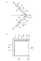
- FIG. 1 It is a front view of the exposure apparatus which concerns on 1st Embodiment of this invention. It is a figure which shows the structure of the lighting apparatus shown in FIG. It is a schematic block diagram of the light source apparatus of 1st Embodiment.
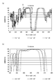
- (A) is a graph which shows the transmissivity of a dichroic mirror which is an example, and (b) is an enlarged view of the IV section of (a).
- (A) is a graph which shows the reflectance of the dichroic mirror of FIG. 4, (b) is an enlarged view of the V section of (a).
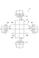
- FIG. 11 is a schematic plan view showing two types of second LED arrays and two dichroic mirrors arranged on a plane perpendicular to the optical axis direction in the case as the light source device of the fourth embodiment. It is a schematic block diagram of the light source apparatus which concerns on the modification of this invention using a dichroic prism. It is a front view of the LED array which is a light source device which concerns on another modification of this invention. It is a front view of the LED array which is the light source device which concerns on still another modification of this invention.
- the proximity exposure apparatus PE uses a mask M smaller than a work W as a material to be exposed, holds the mask M on a mask stage (mask support portion) 1, and holds the work W on a work stage (workpiece).
- the mask M is irradiated with the light for pattern exposure from the illuminating device 3 in a state of being held by the supporting portion 2 and the mask M and the work W are arranged close to each other and face each other with a predetermined exposure gap.
- the pattern of M is exposed and transferred onto the work W.
- the work stage 2 is moved stepwise with respect to the mask M in the biaxial directions of the X axis direction and the Y axis direction, and the exposure transfer is performed for each step.
- an X-axis stage feed mechanism 5 that moves the X-axis feed table 5a stepwise in the X-axis direction is installed on the device base 4.
- a Y-axis stage feed mechanism 6 for step-moving the Y-axis feed base 6a in the Y-axis direction is installed in order to move the work stage 2 in steps in the Y-axis direction.
- a work stage 2 is installed on the Y-axis feed base 6a of the Y-axis stage feed mechanism 6.
- the work W is held on the upper surface of the work stage 2 in a state of being vacuum-sucked by a work chuck or the like. Further, on the side portion of the work stage 2, a substrate side displacement sensor 15 for measuring the height of the lower surface of the mask M is arranged. Therefore, the substrate side displacement sensor 15 can move together with the work stage 2 in the X and Y axis directions.
- a plurality of (four in the embodiment shown in the figure) guide rails 51 of the X-axis linear guides are arranged on the device base 4 in the X-axis direction, and each guide rail 51 has a lower surface of the X-axis feed base 5a.
- a slider 52 fixed to is straddled.
- the X-axis feed base 5a is driven by the first linear motor 20 of the X-axis stage feed mechanism 5 and can reciprocate in the X-axis direction along the guide rail 51.
- a plurality of Y-axis linear guide guide rails 53 are arranged on the X-axis feed base 5a in the Y-axis direction, and each guide rail 53 has a slider 54 fixed to the lower surface of the Y-axis feed base 6a. Is straddled.
- the Y-axis feed base 6a is driven by the second linear motor 21 of the Y-axis stage feed mechanism 6 and can reciprocate in the Y-axis direction along the guide rail 53.
- the vertical coarse movement device 7 Since the work stage 2 is moved in the vertical direction between the Y-axis stage feed mechanism 6 and the work stage 2, the vertical coarse movement device 7 having a relatively coarse positioning resolution but a large movement stroke and movement speed and the vertical coarse movement A vertical fine movement device 8 is installed, which enables positioning with higher resolution than the device 7 and finely adjusts the gap between the facing surfaces of the mask M and the work W to a predetermined amount by finely moving the work stage up and down.
- the vertical coarsening device 7 moves the work stage 2 up and down with respect to the fine movement stage 6b by an appropriate drive mechanism provided in the fine movement stage 6b described later.
- the stage coarse movement shafts 14 fixed at four positions on the bottom surface of the work stage 2 engage with the linear motion bearings 14a fixed to the fine movement stage 6b and are guided in the vertical direction with respect to the fine movement stage 6b. It should be noted that it is desirable that the vertical coarse movement device 7 has a high repeat positioning accuracy even though the resolution is low.
- the vertical fine movement device 8 includes a fixing base 9 fixed to the Y-axis feed base 6a and a guide rail 10 of a linear guide attached to the fixing base 9 with its inner end side inclined diagonally downward.
- a ball screw nut (not shown) is connected to the slide body 12 that reciprocates along the guide rail 10 via the slider 11 straddling the guide rail 10, and the upper end surface of the slide body 12 is connected. Is slidably in contact with the flange 12a fixed to the fine movement stage 6b in the horizontal direction.
- the vertical fine movement device 8 may drive the slide body 12 by a linear motor instead of driving the slide body 12 by the motor 17 and the ball screw.
- This vertical fine movement device 8 is installed at one end in the Y-axis direction (left end side in FIG. 1) of the Z-axis feed base 6a and two at the other end, a total of three units, each of which is independently driven and controlled. It has become so.
- the vertical fine movement device 8 independently finely adjusts the heights of the flanges 12a at the three positions based on the measurement results of the gap amounts between the mask M and the work W at the plurality of positions by the gap sensor 27, and the work stage 2 Finely adjust the height and inclination of. If the height of the work stage 2 can be sufficiently adjusted by the fine vertical movement device 8, the vertical coarse movement device 7 may be omitted.
- a bar mirror (both not shown) facing the interferometer is installed.
- the bar mirror 19 facing the Y-axis laser interferometer 18 is arranged along the X-axis direction on one side of the Y-axis feeder 6a, and the bar mirror facing the X-axis laser interferometer is the Y-axis feeder 6a. It is arranged along the Y-axis direction at one end side.
- the Y-axis laser interferometer 18 and the X-axis laser interferometer are always arranged so as to face the corresponding bar mirrors and supported by the device base 4.
- Two Y-axis laser interferometers 18 are installed so as to be separated from each other in the X-axis direction.
- the two Y-axis laser interferometers 18 detect the position of the Y-axis feed base 6a and, by extension, the work stage 2 in the Y-axis direction and the yawing error via the bar mirror 19.
- the X-axis laser interferometer detects the position in the X-axis direction of the X-axis feed table 5a and by extension, the work stage 2 via the facing bar mirror.
- the mask stage 1 is inserted into the mask base frame 24 made of a substantially rectangular frame and the opening at the center of the mask base frame 24 through a gap in the X, Y, ⁇ directions (in the X, Y plane).
- the mask base frame 24 is movably supported, and the mask base frame 24 is held at a fixed position above the work stage 2 by a column 4 a protruding from the apparatus base 4.
- a frame-shaped mask holder 26 is provided on the lower surface of the central opening of the mask frame 25. That is, a plurality of mask holder suction grooves connected to a vacuum suction device (not shown) are provided on the lower surface of the mask frame 25, and the mask holder 26 sucks the mask frame 25 through the plurality of mask holder suction grooves. Retained.
- a plurality of mask suction grooves for sucking the peripheral portion on which the mask pattern of the mask M is not drawn are provided on the lower surface of the mask holder 26, and the mask M passes through the mask suction grooves. It is detachably held on the lower surface of the mask holder 26 by a vacuum suction device (not shown).
- the lighting device 3 of the exposure device PE of the present embodiment is a plane for changing the direction of the light source device 70 for irradiating ultraviolet rays and the light path EL emitted from the fly-eye lens 65 of the light source device 70.
- a mirror 66, a collimation mirror 67 that irradiates light from the light source device 70 as parallel light, and a flat mirror 68 that irradiates the parallel light toward the mask M are provided.
- the light emitted from the light source device 70 is incident on the incident surface of the fly-eye lens 65.
- the fly-eye lens 65 is used to make the incident light have an illuminance distribution as uniform as possible on the irradiation surface.
- the light emitted from the exit surface of the fly-eye lens 65 is converted into parallel light while its traveling direction is changed by the plane mirror 66, the collimation mirror 67, and the plane mirror 68.
- this parallel light is irradiated as light for pattern exposure substantially perpendicularly to the surface of the mask M held by the mask stage 1 and further the surface of the work W held by the work stage 2, and the pattern of the mask M is changed. It is exposed and transferred onto the work W.
- the light source device 70 of the present embodiment is The first and second LED arrays 71 and 75 emit light having different peak wavelengths, and the photosynthetic element synthesizes light having different peak wavelengths emitted from the first and second LED arrays 71 and 75. It includes a dichroic mirror 80 (80A, 80B) and a fly-eye lens 65 including a plurality of lens elements 65a arranged in a matrix.
- a plurality of first LED elements 72 are arranged two-dimensionally.
- the plurality of first LED elements 72 irradiate UV light having a peak wavelength (first peak wavelength) at any of 360 to 380 nm, for example.
- the peak wavelength of the first LED element 72 is preferably 360 to 370 nm, and more preferably 365 nm.
- a plurality of second LED elements 76 are arranged two-dimensionally.
- the plurality of second LED elements 76 irradiate, for example, UV light having a peak wavelength (second peak wavelength) at either 300 to 355 nm or 385 to 410 nm.
- the peak wavelength of the second LED element 76 is preferably 300 to 355 nm, more preferably 325 to 355 nm, and even more preferably 335 nm.
- the first LED element 72 and the second LED element 76 are selected so that the peak wavelengths of their respective lights are separated by 20 nm or more.
- the reason why the peak wavelengths of the light of the first and second LED elements 72 and 76 are separated by 20 nm or more is that the dichroic mirror 80 needs that the two wavelengths to be combined are separated by 20 nm or more due to its performance. It depends.
- the peak wavelength of the first LED element 72 is set to, for example, 365 nm
- the peak wavelength of the second LED element 76 may be set to 345 nm or less, or may be set to 385 nm or more.
- the dichroic mirror 80 which is a photosynthetic element, forms a thin film (dichroic film) 81 such as a dielectric multilayer film on a plate-shaped transparent medium 82 such as glass or plastic, and reflects light in a specific wavelength band. It is an optical element having a characteristic of transmitting light in other wavelength bands.
- two dichroic mirrors 80A and 80B (two dichroic films 81) having substantially the same length L3 are along the optical axis direction L (that is, along the optical path EL) from the dichroic mirror 80 toward the fly-eye lens 65. It is arranged in a substantially V shape so as to be inclined with respect to the direction) and to be in close contact with the fly-eye lens side.
- the two dichroic mirrors 80A and 80B are combined at an angle of approximately 90 °.
- the first one faces the opening side of the two V-shaped dichroic mirrors 80A and 80B (in the optical axis direction L, the side opposite to the fly eye lens 65 with respect to the dichroic mirror 80, the left side in FIG. 3).
- the LED array 71 is arranged.
- the second LED array is provided on both sides (upper and lower in FIG. 3) of the two V-shaped dichroic mirrors 80A and 80B, which intersect with the optical axis direction L (orthogonal in the present embodiment). 75 are arranged.
- both the first LED array 71 and the second LED array 75 face the V-shaped dichroic mirror 80A or 80B at an angle of approximately 45°.
- the fact that the second LED array 75 is orthogonal to the optical axis direction L is not limited to the case where the second LED array 75 is strictly orthogonal, and the second LED array 75 is incident on the fly-eye lens 65. Including the case where the directionality of light is orthogonal to an allowable degree.
- the number of the second LED elements 76 of the second LED array 75 is half the number of the first LED elements 72 of the first LED array 71. That is, the length L2 of the second LED array 75 is approximately 1 ⁇ 2 of the length L1 of the first LED array 71, and 1 / ⁇ 2 of the length L3 of the dichroic mirror 80A or 80B. Is.
- all the light emitted from the first LED array 71 is transmitted through the dichroic mirror 80A or 80B, and all the light emitted from the two second LED arrays 75 is dichroic mirror 80A or 80B.
- the light reflected from the first LED array 71 and the light emitted from the second LED array 75 are combined and incident on the incident surface of the fly-eye lens 65.
- the two dichroic mirrors 80A and 80B are arranged in a substantially V shape so as to be in close contact with each other on the fly-eye lens 65 side, and the first LED array 71 is arranged in the optical axis direction L.
- the second LED array 75 is arranged on the opposite side of the fly-eye lens 65 with respect to the V-shaped dichroic mirrors 80A and 80B, and the second LED array 75 is orthogonal to the optical axis direction L of the V-shaped dichroic mirrors 80A and 80B.
- the first LED array 71 has a main wavelength having a peak wavelength in any of 360 to 380 nm
- the second LED array 75 has a peak wavelength of, for example, 300 to 355 nm or 385 to 410 nm.
- the sub-wavelength As the sub-wavelength.
- the present embodiment is not limited to this, and the first LED array 71 has a sub-wavelength having a peak wavelength at, for example, 300 to 355 nm or 385 to 410 nm, and the second LED array 75 has a wavelength of 360 to 380 nm. It may be a main wavelength having a peak wavelength in either of them.
- the reflected light by the dichroic mirrors 80A and 80B has better optical efficiency than the transmitted light, it can be appropriately selected according to the photosensitive sensitivity of the resist used.
- the lengths of the first LED array 71, the second LED array 75, and the dichroic mirrors 80A and 80B can also be changed according to the specifications.
- the second LED array 75 passes through the interface of the dichroic mirror 80 once during reflection, whereas the first LED array 71 passes through the interface of the dichroic mirror 80 twice. Further, the light of the second LED array 75 is reflected by the dichroic mirror 80, but since the film thickness of the dichroic mirror 80 is proportional to the reflection wavelength, the shorter the wavelength of the reflected light, the thicker the film thickness. It can be made thinner and easier to manufacture. Therefore, when the dichroic mirror 80 is used, one having a relatively long peak wavelength is applied to the first LED array 71, and one having a relatively short peak wavelength is applied to the second LED array 75. Is preferable.
- preferred combinations of the peak wavelength of the first LED array 71 and the peak wavelength of the second LED array 75 include the following two combinations (A) and (B).
- the exposure sensitivity when the color resist whose absorption peak wavelength range is adjusted to the i-line (365 nm) is exposed by using the LED element having each peak wavelength is confirmed by a test, and is shown in Table 1. The difference in sensitivity was obtained. Table 1 is based on 365 nm.
- the LED element in the long wavelength region (385 nm) is longer than the 365 nm LED element.
- the exposure sensitivity is low, the output is high and the transmittance is high due to the long wavelength.
- the 385 nm LED element arranged in the first LED array 71 has a transmittance of about 98%, and as shown in FIG. 5, the second LED array 75 has a transmittance.
- the arranged 365 nm LED element has a reflectance of about 100%, and the loss as a whole is about 2%.
- FIG. 4 is a graph showing the transmittance of the dichroic mirror 80, which is an example
- FIG. 5 is a graph showing the reflectance of the dichroic mirror 80 of FIG.
- the light emitted from the LED elements 72 and 76 is in the range of angles ⁇ 1 and ⁇ 2 (see FIG. 3) substantially 42 ° to 48 ° with respect to the surfaces of the dichroic mirrors 80A and 80B by the condenser lens.
- the exposure time can be shortened by combining the above two types of LED elements.
- those having a peak wavelength of 365 nm and those having a peak wavelength of 330 nm may be used, and the exposure time can be shortened with the same output.
- the formed pattern can be stabilized.
- the pattern formed depending on the resist is weakly cured, and pattern peeling easily occurs in the developing process.
- the exfoliation is likely to occur at the end of the pattern, and is caused by the leak light passing through the pattern of the mask and the polymerization initiator of the resist.
- both ends 83 of the two dichroic mirrors 80A and 80B are cut in parallel with the optical axis direction L from the dichroic mirror 80 toward the fly-eye lens 65. There is. As a result, the dichroic films 81 of the two dichroic mirrors 80A and 80B are in contact with each other at the top of the V shape, so that the dichroic mirrors 80A and 80B receive the light emitted from the first LED array 71 of the dichroic mirror 80.
- Light can be uniformly transmitted over the entire width direction (direction orthogonal to the optical axis direction L), and the light emitted from the second LED array 75 can be reflected in a wide range, improving efficiency.
- the first LED array 71 and the second LED array 75 can be arranged by exchanging the positions with respect to the two dichroic mirrors 80A and 80B.
- Other configurations and operations are the same as those of the first embodiment of the present invention.
- the dichroic mirror fixing frame 85 three frame bodies 85a, 85b, 85c covering three sides of the four sides of the rectangular dichroic mirrors 80A, 80B are combined in a substantially U-shape, and the dichroic mirrors 80A, 80B have the same shape. It has a shape that opens the side surfaces facing each other. Then, one side surface of the dichroic mirrors 80A and 80B is fitted into the groove 86 formed in the frame body 85a of the substantially U-shaped dichroic mirror fixing frame 85, and the upper surfaces of the dichroic mirrors 80A and 80B are It is pressed toward the frame body 85b by the push screw 87 provided on the frame body 85c via the cushioning material 88, and is fixed to the dichroic mirror fixing frame 85.
- the front end portion 85d of the (frames 85b, 85c) is cut parallel to the optical axis direction L from the dichroic mirror 80 toward the fly-eye lens 65, and adheres so that there is no gap, preferably, there is no gap. ing.
- the tip portion 85d of the dichroic mirror fixing frame 85 (frames 85b, 85c) combined in a V shape on the fly-eye lens side is cut at a right angle to the optical axis direction L from the dichroic mirror 80 toward the fly-eye lens 65, Form planes that are flush with each other.
- the two dichroic mirrors 80A and 80B can be brought closer to the fly-eye lens 65 by the cut length of the dichroic mirror fixing frame 85, the efficiency is improved, and the light source device 70 is made compact.
- the dichroic mirror fixing frame 85 has grooves 86 formed in each of the three frame bodies 85a, 85b, and 85c, and the three grooves 86 are formed.
- Each side (three sides) of the dichroic mirrors 80A and 80B may be fitted to the dichroic mirror 80A and 80B and fixed with an adhesive.
- the tip end portions 83 of the two dichroic mirrors 80A and 80B and the tip end portions 85d of the two dichroic mirror fixing frames 85 are in close contact with each other so that there is no gap. There is no adhesive.
- the light source device 70 of the fourth embodiment will be described with reference to FIG.
- two types of two second LEDs are formed on a plane perpendicular to the optical axis direction L on the side of the two V-shaped dichroic mirrors 80A and 80B.
- Arrays 75A and 75B are arranged. Further, the two second LED arrays 75A and 75A on one side and the two second LED arrays 75B and 75B on the other side are alternately arranged at 90° intervals on the plane.
- the first LED array 71 uses an LED element 72 having a peak wavelength of 365 nm
- the second LED array 75A uses an LED element 76A having a peak wavelength of 385 nm
- the other second LED uses an LED element 76B having a peak wavelength of 330 nm.
- the dichroic mirror 90 is composed of two dichroic mirrors 90A and 90B, like the dichroic mirror 80 described in the first to third embodiments. However, in the present embodiment, the dichroic mirrors 80 and 90 have different characteristics of reflecting the characteristic wavelength band according to the two second LED elements 76A and 76B.
- the dichroic mirror 80 When switching the use of the second LED arrays 75A and 75B, the dichroic mirror 80 when using the first LED array 71 and the one second LED array 75A, the first LED array 71 and the other When the second LED array 75B is used, the dichroic mirror 90 is arranged so that the arrangement directions of the dichroic mirrors 80A, 80B, 90A, and 90B are orthogonal to each other on the plane.
- the second LED arrays 75A and 75B can be replaced by simply replacing the dichroic mirrors 80 and 90. There is no need to replace the second LED arrays 75A and 75B, and the replacement work of the electric system and the cooling system becomes unnecessary.
- the dichroic mirror 80 may be configured to be rotatable when the peak wavelengths of the two types of second LED arrays 75A and 75B are the same. Then, when the LED arrays 75A and 75B are used, the direction of the dichroic mirror 80 is rotated according to the LED arrays 75A and 75B to be used.
- the present invention is not limited to the above-described embodiments, and can be modified, improved, and the like as appropriate.
- the light having different peak wavelengths is described to be combined by the dichroic mirror, but the light combining element of the present invention is not limited to this, and may be a dichroic prism.
- the dichroic prism 180 is a combination of three right-angle prisms 181, 182, 183 made of a material having a high transmittance such as glass or plastic.
- Each prism 181, 182, 183 has a substantially right-angled isosceles triangle shape in a side view, and a prism 181 larger than the prisms 182, 183 is used.
- the dichroic prism 180 has a rectangular shape in a side view in which sides other than the hypotenuse of the prism 181 and the hypotenuses of the prisms 182 and 183 are connected via a dichroic film (not shown).
- the interface 184 of the prisms 181 and 182 on which the dichroic film is arranged and the interface 185 of the prisms 181 and 183 are inclined at approximately 45 ° with respect to the optical axis direction L, and the two interfaces 184 and 185 are 90 °. It is formed to intersect at.
- the two dichroic films are arranged in a substantially V shape so as to be in close contact with each other on the fly-eye lens side.
- the dichroic mirrors arranged in a V shape are used, and the light emitted from the two LED arrays is emitted to the fly-eye lens 65 via the dichroic mirrors.
- the dichroic mirrors 80A and 80B are not provided, and the optical device 70A is composed of only one LED array 78, and the LED array 78 is used as the fly-eye lens 65. They may be arranged directly facing each other.
- the LED array 78 is arranged so that the first LED element 72 and the second LED element 76 are mixed and arranged. Therefore, the light emitted from the LED array 78 is mixed with the light of the first LED element 72 and the light of the second LED element 76, and is emitted to the fly-eye lens 65.
- the peak wavelength of the light emitted from the second LED element 76 is any wavelength of 300 to 355 nm in accordance with the sensitivity of the peak wavelength (photosensitive wavelength) of the polymerization initiator of the photosensitive material.
- the peak wavelength of the light emitted from the LED element 72 of the above is any wavelength in the range of 360 to 380 nm, with the sensitivity adjusted to the absorption hem portion of the polymerization initiator.
- the peak wavelength of the light emitted from the second LED element 76 is set to, for example, 335 nm
- the peak wavelength of the light emitted from the first LED element 72 is set to, for example, 365 nm. ing.
- the resist can be efficiently exposed to light, a photosynthetic element such as a dichroic mirror for synthesizing light is not required, and the LED array 78 can be arranged close to the fly-eye lens 65, resulting in high efficiency. improves. Further, there is no need to restrict the wavelengths of light of the first and second LED elements 72 and 76 by 20 nm or more, and the peak wavelength can be freely set according to the sensitivity of the photosensitive material.
- the light source device 70B may be configured by one dichroic mirror 80 instead of the two dichroic mirrors 80A and 80B arranged in a V shape.
- the first LED array 71 having the plurality of first LED elements 72 and A second LED array 75 having a plurality of second LED elements 76 is arranged orthogonally, and a dichroic mirror 80 is arranged at a 45° angle with respect to the first LED array 71 and the second LED array 75.
- the light emitted from the first LED array 71 passes through the dichroic mirror 80 and enters the fly-eye lens 65, and the light emitted from the second LED array 75 is reflected by the dichroic mirror 80. , It is combined with the light emitted from the first LED array 71 and incident on the fly-eye lens 65.
- the color filter resist is prepared by mixing a polymerization initiator, a pigment, a polymerizable monomer, a polymer, and a solvent.
- a polymerization initiator having an absorption peak in the range of 300 to 355 nm the following (1)
- the items (1) to (10) are listed.
- these polymerization initiators (9) Irgacure OXE01 and (10) Irgacure OXE02, which have high sensitivity, are preferable.
- Omnirad184 registered trademark
- IGM Resins BV 1-hydroxycyclohexyl-phenyl ketone
- Omnirad1173 registered trademark, manufactured by IGM Resins BV (2-hydroxy-2-methyl-1-phenylpropanone)
- Omnirad651 registered trademark
- IGM Resins BV 2,2-dimethoxy-2-phenylacetophenone
- Omnirad2959 (registered trademark), manufactured by IGM Resins BV (1-[4-(2-hydroxyethoxyl)-phenyl]-2-hydroxy-methylpropanone)
- Omnirad127 registered trademark, manufactured by IGM Resins BV (2-hydroxy-1-(4-(4-(2-hydroxy-2-methylpropionyl)benzyl)phenyl)-2-methylpropan-1-one )
- Omnirad369 registered trademark, manufactured by IGM Resins BV (2-benzyl-2- (dimethylamino) -4'-morpholinobutyrophenone)
- Omnirad379EG registered trademark
- IGM Resins BV (2-dimethylamino-2-(4-methyl-benzyl)-1-(4-morpholin-4-yl-phenyl)-butan-1-one )
Landscapes
- Physics & Mathematics (AREA)
- General Physics & Mathematics (AREA)
- Optics & Photonics (AREA)
- Chemical & Material Sciences (AREA)
- Analytical Chemistry (AREA)
- Exposure And Positioning Against Photoresist Photosensitive Materials (AREA)
Abstract
異なるピーク波長を有する複数のLED素子の光を合成可能であり、且つコンパクトに構成された露光用の光源装置、該光源装置を用いた露光装置、及び露光方法を提供する。第1のピーク波長の光を発光する複数の第1のLED素子(72)を有する第1のLEDアレイ(71)と、第1のピーク波長と異なる第2のピーク波長の光を発光する複数の第2のLED素子(76)を有する第2のLEDアレイ(75)と、特定の波長帯域の光を透過させ、その他の波長帯域の光を反射させる2つのダイクロイック膜(81)を備え、第1及び第2のLEDアレイ(71,75)の光を合成する光合成素子(80)と、光合成素子(80)によって合成された光が入射されるフライアイレンズ(65)と、を備える。
Description
本発明は、露光用の光源装置、露光装置、及び露光方法に関し、より詳細には、LED素子から照射される光を光源とする露光用の光源装置、露光装置、及び露光方法に関する。
フラットパネルディスプレイ、プリント基板、及び半導体素子などのリソグラフィーに用いる露光装置において、従来、UV光源として水銀ランプが用いられてきた。しかし、近年、水銀の使用に対する制限が厳しくなり、UV光源のLED化がすすめられている。
ここで、水銀ランプと波長域を合わせた従来のレジストをそのまま用いる場合、単波長のLED素子では、水銀ランプと比べて波長帯域が狭い。そのため、高圧水銀ランプでの出力が強い水銀ランプのg線(436nm)、h線(405nm)、i線(365nm)にあたる、複数の波長のLED素子を組み合わせてUV光源としたものが知られている(例えば、特許文献1及び2参照)。
特許文献1には、高圧水銀ランプでの出力が強いg線(436nm)、h線(405nm)、i線(365nm)にあたる波長の光を照射する複数のLED素子からのUV光を、X字型のダイクロイックミラーを用いて合波させた光源装置が記載されている。また、特許文献2には、360nm~380nm、390nm~410nm、420nm~450nmの波長帯でそれぞれUV光を発光する複数のLED光源と、それぞれのLED光源に対して配置された複数のダイクロイックミラーとを備えるLED型紫外線照射器が記載されている。さらに、特許文献2では、300nm未満の波長、例えば名目上240nmの波長で発行するUV LED光を用いることが記載されている。
ところで、UV光源の設定波長は、効率よくレジストを感光させられる波長のほうが、LED光源の消費電力が少なく、また、光源の発熱による冷却の手間を減らすことができ、好ましい。露光装置では、一般に、部品数の低減、装置内のスペースの有効活用、及び軽量化のため、UV光源をコンパクト化したいという要請がある。LEDアレイからの光は、個々のLED素子に集光レンズがついているものの、特に、凸レンズなどの光学部材を別途用いないと光が平行にならず、拡散する傾向がある。このため、光路長を短くし、
光源装置をコンパクトにする必要性が高い。特に、ディスプレイ向けの露光装置では、一度に広い面積を露光する必要があるため、光源サイズも大きくなり、コンパクト化の必要性が高い。
光源装置をコンパクトにする必要性が高い。特に、ディスプレイ向けの露光装置では、一度に広い面積を露光する必要があるため、光源サイズも大きくなり、コンパクト化の必要性が高い。
特許文献1に記載の光源装置は、X字型のダイクロイックミラーを用いて設置面積の低減を図っているが、さらにコンパクト化する余地があった。また、特許文献2に記載のLED型紫外線照射器は、3個以上のダイクロイックミラーを直列に用いており、コンパクトなLED光源としてはさらに改善の余地があった。
また、発明者が従来のレジストを用いて試験したところ、i線(365nm)より短波長での露光感度が高いレジストが見つかった。これは、レジストの重合開始剤が、吸収ピーク波長だけでなく周辺の波長にも吸収を持つが、吸収する波長域が、可視光域まで伸びると、レジストの用途により問題を生ずることがあるため、あえて、吸収ピーク波長を、水銀ランプのg線、h線、i線より短波長に設定しているため、と考えられる。このような用途としては、例えば、ディスプレイやイメージセンサのカラーフィルター用のレジストがあげられる。したがって、このようなレジストをより効率良く感光させる、光源装置も望まれていた。
本発明は、前述した課題に鑑みてなされたものであり、その目的は、異なるピーク波長を有する複数のLED素子の光を合成し、且つコンパクトに構成された露光用の光源装置、該光源装置を用いた露光装置、及び露光方法を提供することにある。
本発明の上記目的は、下記の構成により達成される。
(1) 第1のピーク波長の光を発光する複数の第1のLED素子を有する第1のLEDアレイと、
第1のピーク波長と異なる第2のピーク波長の光を発光する複数の第2のLED素子を有する第2のLEDアレイと、
該第1及び第2のLEDアレイの光を合成する光合成素子と、
前記光合成素子によって合成された光が入射されるフライアイレンズと、
を備える、露光用の光源装置であって、
前記光合成素子は、特定の波長帯域の光を透過させ、その他の波長帯域の光を反射させる2つのダイクロイック膜を備え、該2つのダイクロイック膜は、前記光合成素子から前記フライアイレンズに向かう光軸方向に対して傾斜し、且つ、前記フライアイレンズ側で密着するように略V字形に配置され、
前記第1のLEDアレイは、前記光軸方向において、前記光合成素子に対して前記フライアイレンズの反対側に配置され、
前記第2のLEDアレイは、前記光軸方向に対して交差して、前記光合成素子の側方に配置される、露光用の光源装置。
(2) 前記第1のLED素子と前記第2のLED素子のいずれか一方から照射される光のピーク波長は、360~380nmであり、
前記第1のLED素子と前記第2のLED素子のいずれか他方から照射される光のピーク波長は、300~355nm又は385~410nmであり、
前記第1のLED素子と前記第2のLED素子の各ピーク波長は、20nm以上離れている、(1)に記載の露光用の光源装置。
(3) 前記光合成素子の側方に配置される前記第2のLEDアレイの長さは、
前記光合成素子に対して前記フライアイレンズの反対側に配置される前記第1のLEDアレイの長さより短い、(1)又は(2)に記載の露光用の光源装置。
(4) 前記光合成素子は、2枚のダイクロイックミラーまたはダイクロイックプリズムである、(1)~(3)のいずれかに記載の露光用の光源装置。
(5) 前記光合成素子は、前記ダイクロイック膜をそれぞれ有する2枚のダイクロイックミラーであって、
前記各ダイクロイックミラーの端部は、前記光軸方向と平行にカットされる、(1)に記載の露光用の光源装置。
(6) 前記ダイクロイックミラーがそれぞれ固定され、前記2枚のダイクロイックミラーが互いに密着する側において開放された2つのダイクロイックミラー固定枠をさらに備え、
前記ダイクロイックミラー固定枠の前記フライアイレンズ側の先端は、前記光軸方向と直角にカットされる、(5)に記載の露光用の光源装置。
(7) 前記第2のLEDアレイは、前記光軸方向に対して直交する平面上に、90°間隔で交互に配置される、2種類の2つの第2のLEDアレイを有する、(1)~(6)のいずれかに記載の露光用の光源装置。
(8) (1)~(7)のいずれかに記載の露光用の光源装置を有する照明装置と、
ワークを支持するワーク支持部と、
マスクを支持しるマスク支持部と、
を備え、前記照明装置から照射される光を、前記マスクを介して前記ワークに照射して前記マスクのパターンを前記ワークに転写する露光装置。
(9) (8)に記載の露光装置を用いて、前記照明装置から照射される光を、前記マスクを介して前記ワークに照射して前記マスクのパターンを前記ワークに転写する露光方法。
(10) 基板に設けられた感光材料の重合開始剤の感光波長に対応する、360~380nmの範囲に第1のピーク波長の光を発光する複数の第1のLED素子と、300~355nmの範囲に第2のピーク波長の光を発光する複数の第2のLED素子と、
を備え、
前記第1のLED素子の光と前記第2のLED素子の光が、混合してフライアイレンズに出射される、露光用の光源装置。
(11) 前記第1のLED素子及び前記第2のLED素子が混在して配置されるLEDアレイを備える、(10)に記載の露光用の光源装置。
(12) 前記複数の第1のLED素子を有する第1のLEDアレイと、
前記複数の第2のLED素子を有する第2のLEDアレイと、
該第1及び第2のLEDアレイの光を合成する光合成素子と、
を備え、
前記光合成素子は、特定の波長帯域の光を透過させ、その他の波長帯域の光を反射させるダイクロイック膜を、前記光合成素子から前記フライアイレンズに向かう光軸方向に対して傾斜して配置し、
前記第1のLEDアレイと前記第2のLEDアレイのいずれか一方は、前記光軸方向において、前記光合成素子に対して前記フライアイレンズの反対側に配置され、
前記第1のLEDアレイと前記第2のLEDアレイのいずれか他方は、前記光軸方向に対して交差して、前記光合成素子の側方に配置される、(9)に記載の露光用の光源装置。
(13) (10)~(12)のいずれかに記載の露光用の光源装置を有する照明装置と、
ワークを支持するワーク支持部と、
マスクを支持しるマスク支持部と、
を備え、前記照明装置から照射される光を、前記マスクを介して前記ワークに照射して前記マスクのパターンを前記ワークに転写する露光装置。
(14) (13)に記載の露光装置を用いて、前記照明装置から照射される光を、前記マスクを介して前記ワークに照射して前記マスクのパターンを前記ワークに転写する露光方法。
(1) 第1のピーク波長の光を発光する複数の第1のLED素子を有する第1のLEDアレイと、
第1のピーク波長と異なる第2のピーク波長の光を発光する複数の第2のLED素子を有する第2のLEDアレイと、
該第1及び第2のLEDアレイの光を合成する光合成素子と、
前記光合成素子によって合成された光が入射されるフライアイレンズと、
を備える、露光用の光源装置であって、
前記光合成素子は、特定の波長帯域の光を透過させ、その他の波長帯域の光を反射させる2つのダイクロイック膜を備え、該2つのダイクロイック膜は、前記光合成素子から前記フライアイレンズに向かう光軸方向に対して傾斜し、且つ、前記フライアイレンズ側で密着するように略V字形に配置され、
前記第1のLEDアレイは、前記光軸方向において、前記光合成素子に対して前記フライアイレンズの反対側に配置され、
前記第2のLEDアレイは、前記光軸方向に対して交差して、前記光合成素子の側方に配置される、露光用の光源装置。
(2) 前記第1のLED素子と前記第2のLED素子のいずれか一方から照射される光のピーク波長は、360~380nmであり、
前記第1のLED素子と前記第2のLED素子のいずれか他方から照射される光のピーク波長は、300~355nm又は385~410nmであり、
前記第1のLED素子と前記第2のLED素子の各ピーク波長は、20nm以上離れている、(1)に記載の露光用の光源装置。
(3) 前記光合成素子の側方に配置される前記第2のLEDアレイの長さは、
前記光合成素子に対して前記フライアイレンズの反対側に配置される前記第1のLEDアレイの長さより短い、(1)又は(2)に記載の露光用の光源装置。
(4) 前記光合成素子は、2枚のダイクロイックミラーまたはダイクロイックプリズムである、(1)~(3)のいずれかに記載の露光用の光源装置。
(5) 前記光合成素子は、前記ダイクロイック膜をそれぞれ有する2枚のダイクロイックミラーであって、
前記各ダイクロイックミラーの端部は、前記光軸方向と平行にカットされる、(1)に記載の露光用の光源装置。
(6) 前記ダイクロイックミラーがそれぞれ固定され、前記2枚のダイクロイックミラーが互いに密着する側において開放された2つのダイクロイックミラー固定枠をさらに備え、
前記ダイクロイックミラー固定枠の前記フライアイレンズ側の先端は、前記光軸方向と直角にカットされる、(5)に記載の露光用の光源装置。
(7) 前記第2のLEDアレイは、前記光軸方向に対して直交する平面上に、90°間隔で交互に配置される、2種類の2つの第2のLEDアレイを有する、(1)~(6)のいずれかに記載の露光用の光源装置。
(8) (1)~(7)のいずれかに記載の露光用の光源装置を有する照明装置と、
ワークを支持するワーク支持部と、
マスクを支持しるマスク支持部と、
を備え、前記照明装置から照射される光を、前記マスクを介して前記ワークに照射して前記マスクのパターンを前記ワークに転写する露光装置。
(9) (8)に記載の露光装置を用いて、前記照明装置から照射される光を、前記マスクを介して前記ワークに照射して前記マスクのパターンを前記ワークに転写する露光方法。
(10) 基板に設けられた感光材料の重合開始剤の感光波長に対応する、360~380nmの範囲に第1のピーク波長の光を発光する複数の第1のLED素子と、300~355nmの範囲に第2のピーク波長の光を発光する複数の第2のLED素子と、
を備え、
前記第1のLED素子の光と前記第2のLED素子の光が、混合してフライアイレンズに出射される、露光用の光源装置。
(11) 前記第1のLED素子及び前記第2のLED素子が混在して配置されるLEDアレイを備える、(10)に記載の露光用の光源装置。
(12) 前記複数の第1のLED素子を有する第1のLEDアレイと、
前記複数の第2のLED素子を有する第2のLEDアレイと、
該第1及び第2のLEDアレイの光を合成する光合成素子と、
を備え、
前記光合成素子は、特定の波長帯域の光を透過させ、その他の波長帯域の光を反射させるダイクロイック膜を、前記光合成素子から前記フライアイレンズに向かう光軸方向に対して傾斜して配置し、
前記第1のLEDアレイと前記第2のLEDアレイのいずれか一方は、前記光軸方向において、前記光合成素子に対して前記フライアイレンズの反対側に配置され、
前記第1のLEDアレイと前記第2のLEDアレイのいずれか他方は、前記光軸方向に対して交差して、前記光合成素子の側方に配置される、(9)に記載の露光用の光源装置。
(13) (10)~(12)のいずれかに記載の露光用の光源装置を有する照明装置と、
ワークを支持するワーク支持部と、
マスクを支持しるマスク支持部と、
を備え、前記照明装置から照射される光を、前記マスクを介して前記ワークに照射して前記マスクのパターンを前記ワークに転写する露光装置。
(14) (13)に記載の露光装置を用いて、前記照明装置から照射される光を、前記マスクを介して前記ワークに照射して前記マスクのパターンを前記ワークに転写する露光方法。
本発明の露光用の光源装置、該光源装置を用いた露光装置、及び露光方法によれば、ピーク波長の異なる複数のLED素子からの光を合成可能な光源装置をコンパクトに構成すると共に、該合成光により効率よく感光材料を感光させて、露光作業効率を向上させることができる。
(第1実施形態)
以下、本発明に係る露光装置の第1実施形態を図面に基づいて詳細に説明する。図1に示すように、近接露光装置PEは、被露光材としてのワークWより小さいマスクMを用い、マスクMをマスクステージ(マスク支持部)1で保持すると共に、ワークWをワークステージ(ワーク支持部)2で保持し、マスクMとワークWとを近接させて所定の露光ギャップで対向配置した状態で、照明装置3からパターン露光用の光をマスクMに向けて照射することにより、マスクMのパターンをワークW上に露光転写する。また、ワークステージ2をマスクMに対してX軸方向とY軸方向の二軸方向にステップ移動させて、ステップ毎に露光転写が行われる。
以下、本発明に係る露光装置の第1実施形態を図面に基づいて詳細に説明する。図1に示すように、近接露光装置PEは、被露光材としてのワークWより小さいマスクMを用い、マスクMをマスクステージ(マスク支持部)1で保持すると共に、ワークWをワークステージ(ワーク支持部)2で保持し、マスクMとワークWとを近接させて所定の露光ギャップで対向配置した状態で、照明装置3からパターン露光用の光をマスクMに向けて照射することにより、マスクMのパターンをワークW上に露光転写する。また、ワークステージ2をマスクMに対してX軸方向とY軸方向の二軸方向にステップ移動させて、ステップ毎に露光転写が行われる。
ワークステージ2をX軸方向にステップ移動させるため、装置ベース4上には、X軸送り台5aをX軸方向にステップ移動させるX軸ステージ送り機構5が設置されている。X軸ステージ送り機構5のX軸送り台5a上には、ワークステージ2をY軸方向にステップ移動させるため、Y軸送り台6aをY軸方向にステップ移動させるY軸ステージ送り機構6が設置されている。Y軸ステージ送り機構6のY軸送り台6a上には、ワークステージ2が設置されている。ワークステージ2の上面には、ワークWがワークチャック等で真空吸引された状態で保持される。また、ワークステージ2の側部には、マスクMの下面高さを測定するための基板側変位センサ15が配設されている。従って、基板側変位センサ15は、ワークステージ2と共にX、Y軸方向に移動可能である。
装置ベース4上には、複数(図に示す実施形態では4本)のX軸リニアガイドのガイドレール51がX軸方向に配置され、それぞれのガイドレール51には、X軸送り台5aの下面に固定されたスライダ52が跨架されている。これにより、X軸送り台5aは、X軸ステージ送り機構5の第1リニアモータ20で駆動され、ガイドレール51に沿ってX軸方向に往復移動可能である。また、X軸送り台5a上には、複数のY軸リニアガイドのガイドレール53がY軸方向に配置され、それぞれのガイドレール53には、Y軸送り台6aの下面に固定されたスライダ54が跨架されている。これにより、Y軸送り台6aは、Y軸ステージ送り機構6の第2リニアモータ21で駆動され、ガイドレール53に沿ってY軸方向に往復移動可能である。
Y軸ステージ送り機構6とワークステージ2の間には、ワークステージ2を上下方向に移動させるため、比較的位置決め分解能は粗いが移動ストローク及び移動速度が大きな上下粗動装置7と、上下粗動装置7と比べて高分解能での位置決めが可能でワークステージを上下に微動させてマスクMとワークWとの対向面間のギャップを所定量に微調整する上下微動装置8が設置されている。
上下粗動装置7は後述の微動ステージ6bに設けられた適宜の駆動機構によりワークステージ2を微動ステージ6bに対して上下動させる。ワークステージ2の底面の4箇所に固定されたステージ粗動軸14は、微動ステージ6bに固定された直動ベアリング14aに係合し、微動ステージ6bに対し上下方向に案内される。なお、上下粗動装置7は、分解能が低くても、繰り返し位置決め精度が高いことが望ましい。
上下微動装置8は、Y軸送り台6aに固定された固定台9と、固定台9にその内端側を斜め下方に傾斜させた状態で取り付けられたリニアガイドの案内レール10とを備えており、該案内レール10に跨架されたスライダ11を介して案内レール10に沿って往復移動するスライド体12にボールねじのナット(図示せず)が連結されると共に、スライド体12の上端面は微動ステージ6bに固定されたフランジ12aに対して水平方向に摺動自在に接している。
そして、固定台9に取り付けられたモータ17によってボールねじのねじ軸を回転駆動させると、ナット、スライダ11及びスライド体12が一体となって案内レール10に沿って斜め方向に移動し、これにより、フランジ12aが上下微動する。
なお、上下微動装置8は、モータ17とボールねじによってスライド体12を駆動する代わりに、リニアモータによってスライド体12を駆動するようにしてもよい。
なお、上下微動装置8は、モータ17とボールねじによってスライド体12を駆動する代わりに、リニアモータによってスライド体12を駆動するようにしてもよい。
この上下微動装置8は、Z軸送り台6aのY軸方向の一端側(図1の左端側)に1台、他端側に2台、合計3台設置されてそれぞれが独立に駆動制御されるようになっている。これにより、上下微動装置8は、ギャップセンサ27による複数箇所でのマスクMとワークWとのギャップ量の計測結果に基づき、3箇所のフランジ12aの高さを独立に微調整してワークステージ2の高さ及び傾きを微調整する。
なお、上下微動装置8によってワークステージ2の高さを十分に調整できる場合には、上下粗動装置7を省略してもよい。
なお、上下微動装置8によってワークステージ2の高さを十分に調整できる場合には、上下粗動装置7を省略してもよい。
また、Y軸送り台6a上には、ワークステージ2のY方向の位置を検出するY軸レーザ干渉計18に対向するバーミラー19と、ワークステージ2のX軸方向の位置を検出するX軸レーザ干渉計に対向するバーミラー(共に図示せず)とが設置されている。Y軸レーザ干渉計18に対向するバーミラー19は、Y軸送り台6aの一側でX軸方向に沿って配置されており、X軸レーザ干渉計に対向するバーミラーは、Y軸送り台6aの一端側でY軸方向に沿って配置されている。
Y軸レーザ干渉計18及びX軸レーザ干渉計は、それぞれ常に対応するバーミラーに対向するように配置されて装置ベース4に支持されている。なお、Y軸レーザ干渉計18は、X軸方向に離間して2台設置されている。2台のY軸レーザ干渉計18により、バーミラー19を介してY軸送り台6a、ひいてはワークステージ2のY軸方向の位置及びヨーイング誤差を検出する。また、X軸レーザ干渉計により、対向するバーミラーを介してX軸送り台5a、ひいてはワークステージ2のX軸方向の位置を検出する。
マスクステージ1は、略長方形状の枠体からなるマスク基枠24と、該マスク基枠24の中央部開口にギャップを介して挿入されてX,Y,θ方向(X,Y平面内)に移動可能に支持されたマスクフレーム25とを備えており、マスク基枠24は装置ベース4から突設された支柱4aによってワークステージ2の上方の定位置に保持されている。
マスクフレーム25の中央部開口の下面には、枠状のマスクホルダ26が設けられている。即ち、マスクフレーム25の下面には、図示しない真空式吸着装置に接続される複数のマスクホルダ吸着溝が設けられており、マスクホルダ26が複数のマスクホルダ吸着溝を介してマスクフレーム25に吸着保持される。
マスクホルダ26の下面には、マスクMのマスクパターンが描かれていない周縁部を吸着するための複数のマスク吸着溝(図示せず)が開設されており、マスクMは、マスク吸着溝を介して図示しない真空式吸着装置によりマスクホルダ26の下面に着脱自在に保持される。
図2に示すように、本実施形態の露光装置PEの照明装置3は、紫外線照射用の光源装置70と、光源装置70のフライアイレンズ65から出射された光路ELの向きを変えるための平面ミラー66と、光源装置70からの光を平行光として照射するコリメーションミラー67と、該平行光をマスクMに向けて照射する平面ミラー68と、を備える。
照明装置3では、光源装置70から照射された光が、フライアイレンズ65の入射面に入射される。フライアイレンズ65は、入射した光を照射面においてできるだけ均一な照度分布とするために使用される。そして、フライアイレンズ65の出射面から発せられた光は、平面ミラー66、コリメーションミラー67、及び平面ミラー68によってその進行方向が変えられるとともに平行光に変換される。そして、この平行光は、マスクステージ1に保持されるマスクM、さらにはワークステージ2に保持されるワークWの表面に対して略垂直にパターン露光用の光として照射され、マスクMのパターンがワークW上に露光転写される。
次に、図3を参照して光源装置70について詳述する。本実施形態の光源装置70は、
互いにピーク波長の異なる光を照射する第1及び第2のLEDアレイ71,75と、該第1及び第2のLEDアレイ71,75から照射されるピーク波長が異なる光を合成する光合成素子であるダイクロイックミラー80(80A,80B)と、マトリックス状に配列された複数のレンズ素子65aを備えるフライアイレンズ65とを備える。
互いにピーク波長の異なる光を照射する第1及び第2のLEDアレイ71,75と、該第1及び第2のLEDアレイ71,75から照射されるピーク波長が異なる光を合成する光合成素子であるダイクロイックミラー80(80A,80B)と、マトリックス状に配列された複数のレンズ素子65aを備えるフライアイレンズ65とを備える。
第1のLEDアレイ71は、複数の第1のLED素子72が二次元に整列配置されている。複数の第1のLED素子72は、例えば、360~380nmのいずれかにピーク波長(第1のピーク波長)を有するUV光を照射する。なお、第1のLED素子72のピーク波長は、好ましくは、360~370nmであり、より好ましくは365nmである。
第2のLEDアレイ75は、複数の第2のLED素子76が二次元に整列配置されている。複数の第2のLED素子76は、例えば、300~355nm又は385~410nmのいずれかにピーク波長(第2のピーク波長)を有するUV光を照射する。なお、第2のLED素子76のピーク波長は、300~355nmのほうが好ましく、より好ましくは、325~355nmであり、さらに好ましくは335nmである。
なお、第1のLED素子72と第2のLED素子76は、それぞれの光のピーク波長が20nm以上離間するように選定される。第1及び第2のLED素子72,76の光のピーク波長を20nm以上離間する理由は、ダイクロイックミラー80は、その性能上から合成する2つの波長が20nm以上離間していることが必要であることによる。
なお、第1のLED素子72のピーク波長が、例えば、365nmに設定された場合、
第2のLED素子76のピーク波長は、345nm以下に設定されてもよいが、又は385nm以上に設定されてもよい。
第2のLED素子76のピーク波長は、345nm以下に設定されてもよいが、又は385nm以上に設定されてもよい。
光合成素子であるダイクロイックミラー80は、誘電体の多層膜などの薄膜(ダイクロイック膜)81をガラスやプラスチック等の板状の透明媒質82上に形成して、特定の波長帯域の光は反射し、それ以外の波長帯域の光を透過する特性を有する光学素子である。
ダイクロイックミラー80は、略等しい長さL3の2枚のダイクロイックミラー80A,80B(2つのダイクロイック膜81)が、ダイクロイックミラー80からフライアイレンズ65に向かう光軸方向L(即ち、光路ELに沿った方向)に対して傾斜し、且つ、フライアイレンズ側で密着するように略V字形に配置されている。なお、本実施形態では、
2枚のダイクロイックミラー80A,80Bは、略90°の角度で組み合わされている。
ダイクロイックミラー80は、略等しい長さL3の2枚のダイクロイックミラー80A,80B(2つのダイクロイック膜81)が、ダイクロイックミラー80からフライアイレンズ65に向かう光軸方向L(即ち、光路ELに沿った方向)に対して傾斜し、且つ、フライアイレンズ側で密着するように略V字形に配置されている。なお、本実施形態では、
2枚のダイクロイックミラー80A,80Bは、略90°の角度で組み合わされている。
そして、V字形の2枚のダイクロイックミラー80A,80Bの開口側(光軸方向Lにおいて、ダイクロイックミラー80に対してフライアイレンズ65と反対側、図3においては左側)に対向して第1のLEDアレイ71が配置される。また、光軸方向Lに対して交差(本実施形態では、直交)して、V字形の2枚のダイクロイックミラー80A,80Bの両側方(図3において上下)には、それぞれ第2のLEDアレイ75が配置されている。これにより、第1のLEDアレイ71及び第2のLEDアレイ75は、いずれもV字形のダイクロイックミラー80A,又は80Bに対して略45°の角度で対向する。
なお、本実施形態において、第2のLEDアレイ75が光軸方向Lに対して直交するとは、厳密に直交する場合だけでなく、フライアイレンズ65に入射される第2のLEDアレイ75からの光の方向性が許容される程度に直交する場合を含む。
なお、本実施形態において、第2のLEDアレイ75が光軸方向Lに対して直交するとは、厳密に直交する場合だけでなく、フライアイレンズ65に入射される第2のLEDアレイ75からの光の方向性が許容される程度に直交する場合を含む。
なお、第2のLEDアレイ75の第2のLED素子76の数は、第1のLEDアレイ71の第1のLED素子72の数の1/2である。即ち、第2のLEDアレイ75の長さL2は、第1のLEDアレイ71の長さL1の略1/2の長さであり、ダイクロイックミラー80A、又は80Bの長さL3の1/√2である。これにより、第1のLEDアレイ71から照射されたすべての光がダイクロイックミラー80A、又は80Bを透過すると共に、2つの第2のLEDアレイ75から照射されたすべての光がダイクロイックミラー80A、又は80Bで反射され、第1のLEDアレイ71から照射された光と、第2のLEDアレイ75から照射された光が合成されて、フライアイレンズ65の入射面に入射される。
このように、2枚のダイクロイックミラー80A,80Bを、フライアイレンズ65側で密着するように略V字形に配置し、第1のLEDアレイ71を、光軸方向Lにおいて、
V字形のダイクロイックミラー80A,80Bに対してフライアイレンズ65の反対側に配置し、第2のLEDアレイ75を、光軸方向Lに対して直交して、V字形のダイクロイックミラー80A,80Bの両側方に分割して配置することで、第1のLEDアレイ71からフライアイレンズ65までの長さを短くすることができ、光源装置70をコンパクトに構成することができる。また、第1のLEDアレイ71とフライアイレンズ65が近接配置されることで、光学効率が向上する。
V字形のダイクロイックミラー80A,80Bに対してフライアイレンズ65の反対側に配置し、第2のLEDアレイ75を、光軸方向Lに対して直交して、V字形のダイクロイックミラー80A,80Bの両側方に分割して配置することで、第1のLEDアレイ71からフライアイレンズ65までの長さを短くすることができ、光源装置70をコンパクトに構成することができる。また、第1のLEDアレイ71とフライアイレンズ65が近接配置されることで、光学効率が向上する。
なお、図3では、第1のLEDアレイ71を360~380nmのいずれかにピーク波長を有する主波長、第2のLEDアレイ75を、例えば、300~355nm又は385~410nmのいずれかにピーク波長を有する副波長としている。しかしながら、本実施形態では、これに限らず、第1のLEDアレイ71を例えば、300~355nm又は385~410nmのいずれかにピーク波長を有する副波長、第2のLEDアレイ75を360~380nmのいずれかにピーク波長を有する主波長としてもよい。
また、ダイクロイックミラー80A,80Bによる反射光は、透過光より光学効率がよいため、使用されるレジストの感光感度に応じて適宜選択可能である。また、第1のLEDアレイ71、第2のLEDアレイ75、及びダイクロイックミラー80A,80Bの長さも、仕様に合わせて変更することができる。
第2のLEDアレイ75は、反射の際、ダイクロイックミラー80の界面を1回通過するのに対し、第1のLEDアレイ71は、ダイクロイックミラー80の界面を2回通過する。また、第2のLEDアレイ75の光は、ダイクロイックミラー80で反射されるが、ダイクロイックミラー80の膜厚は、反射波長に比例するため、反射される光の波長が短い方が、膜厚を薄くすることが可能で、製造が容易となる。このため、ダイクロイックミラー80を使用する場合、第1のLEDアレイ71にはピーク波長が相対的に長いものを適用し、第2のLEDアレイ75にはピーク波長が相対的に短いものを適用するのが好ましい。
具体的に、第1のLEDアレイ71のピーク波長と第2のLEDアレイ75のピーク波長の好ましい組み合わせとしては、次の2つの組み合わせ(A),(B)が挙げられる。
(A)第1のLEDアレイ71のピーク波長:360~380nm
第2のLEDアレイ75のピーク波長:300~355nm
(B)第1のLEDアレイ71のピーク波長:385~410nm
第2のLEDアレイ75のピーク波長:360~380nm
(A)第1のLEDアレイ71のピーク波長:360~380nm
第2のLEDアレイ75のピーク波長:300~355nm
(B)第1のLEDアレイ71のピーク波長:385~410nm
第2のLEDアレイ75のピーク波長:360~380nm
また、一般に、i線(365nm)に吸収ピーク波長域を合わせるカラーレジストに対して、各ピーク波長を有するLED素子を用いて露光した場合の露光感度を試験により確認したところ、表1に示すような感度差が得られた。なお、表1は、365nmを基準としている。

表1からわかるように、例えば、365nmの波長の光に対して330nmの波長の光は露光感度が3倍であるので、365nmのLED素子の出力が30%程度でも同等性能が得られる。よって、レジストの吸収ピーク波長域に合わせて、2種類のLED素子を組み合わせることで、露光時間の短縮による露光工程の効率化が可能となる。
一例として、第2のLED素子76を主波長である365nmとし、第1のLED素子72を副波長の385nmとした場合、長波長域(385nm)のLED素子は、365nmのLED素子に比べて、露光感度は低いものの、出力が高く、また、波長が長い分、透過率が高い。具体的に、図4に示すように、第1のLEDアレイ71に配置された385nmのLED素子は、透過率が約98%であり、図5に示すように、第2のLEDアレイ75に配置された365nmのLED素子は、反射率が略100%であり、全体として約2%の損失で済む。なお、図4は、一例であるダイクロイックミラー80の透過率を示すグラフであり、図5は、図4のダイクロイックミラー80の反射率を示すグラフである。各グラフは、各LED素子72,76から出射される光が、集光レンズにより、ダイクロイックミラー80A,80Bの表面に対して実質42°~48°の角度θ1、θ2(図3参照)の範囲でダイクロイックミラー80A,80Bに入射されるとして、θ1、θ2=42°、45°、48°での透過率、反射率を示している。
このように、上記2種類のLED素子を組み合わせることで、露光時間を短縮することができる。なお、2種類のLED素子の組み合わせとしては、ピーク波長が365nmのものと、330nmのものとを用いてもよく、同一出力として露光時間を短縮することができる。
さらに、主波長となるLED素子と、主波長よりも長い波長を有するLED素子とを組み合わせることで、形成するパターンの安定化が図られる。
例えば、ピーク波長が365nmの単波長のLED素子のみを用いて露光した場合、レジストによっては形成されるパターンの硬化が弱く、現像工程においてパターンのはく離が起こりやすい。はく離は、パターンの端部で発生しやすく、マスクのパターンを通る漏れ光と、レジストの重合開始剤に起因する。通常、はく離の抑制には、露光時間を増やす、又は、前後工程の調整が必要となるが、本例のように、出力が高く、また波長が長い分だけレジストに対する透過率が高く、レジスト深部まで光が届きやすい、385nmの波長を有するLED素子を組み合わせて用いることで、パターンの安定化を図ることができる。
例えば、ピーク波長が365nmの単波長のLED素子のみを用いて露光した場合、レジストによっては形成されるパターンの硬化が弱く、現像工程においてパターンのはく離が起こりやすい。はく離は、パターンの端部で発生しやすく、マスクのパターンを通る漏れ光と、レジストの重合開始剤に起因する。通常、はく離の抑制には、露光時間を増やす、又は、前後工程の調整が必要となるが、本例のように、出力が高く、また波長が長い分だけレジストに対する透過率が高く、レジスト深部まで光が届きやすい、385nmの波長を有するLED素子を組み合わせて用いることで、パターンの安定化を図ることができる。
(第2実施形態)
次に、第2実施形態の光源装置70について図6を参照して説明する。図6に示すように、本実施形態の光源装置70は、2枚のダイクロイックミラー80A,80Bの両端部83が、ダイクロイックミラー80からフライアイレンズ65に向かう光軸方向Lと平行にカットされている。これにより、2枚のダイクロイックミラー80A,80Bの互いのダイクロイック膜81がV字形の頂部で接するので、ダイクロイックミラー80A,80Bは、第1のLEDアレイ71から照射される光を、ダイクロイックミラー80の幅方向
(光軸方向Lに直交する方向)全域に亘って均一に透過すると共に、第2のLEDアレイ75から照射される光を広い範囲で反射することができ、効率が向上する。
なお、この場合も、第1のLEDアレイ71と第2のLEDアレイ75は、2枚のダイクロイックミラー80A,80Bに対する位置を入れ換えて配置することができる。
その他の構成及び作用については、本発明の第1実施形態のものと同様である。
次に、第2実施形態の光源装置70について図6を参照して説明する。図6に示すように、本実施形態の光源装置70は、2枚のダイクロイックミラー80A,80Bの両端部83が、ダイクロイックミラー80からフライアイレンズ65に向かう光軸方向Lと平行にカットされている。これにより、2枚のダイクロイックミラー80A,80Bの互いのダイクロイック膜81がV字形の頂部で接するので、ダイクロイックミラー80A,80Bは、第1のLEDアレイ71から照射される光を、ダイクロイックミラー80の幅方向
(光軸方向Lに直交する方向)全域に亘って均一に透過すると共に、第2のLEDアレイ75から照射される光を広い範囲で反射することができ、効率が向上する。
なお、この場合も、第1のLEDアレイ71と第2のLEDアレイ75は、2枚のダイクロイックミラー80A,80Bに対する位置を入れ換えて配置することができる。
その他の構成及び作用については、本発明の第1実施形態のものと同様である。
(第3実施形態)
次に、第3実施形態の光源装置70について図7を参照して説明する。図7に示すように、本実施形態は、2つのダイクロイックミラー固定枠85を用いて、上記実施形態で説明した2枚のダイクロイックミラー80A,80Bの固定方法について説明する。
次に、第3実施形態の光源装置70について図7を参照して説明する。図7に示すように、本実施形態は、2つのダイクロイックミラー固定枠85を用いて、上記実施形態で説明した2枚のダイクロイックミラー80A,80Bの固定方法について説明する。
ダイクロイックミラー固定枠85は、矩形状のダイクロイックミラー80A,80Bの4辺のうち、3辺を覆う3本の枠体85a,85b,85cが略コの字形に組み合わされ、ダイクロイックミラー80A,80Bの互いに対向する側の側面を開放する形状を有する。そして、ダイクロイックミラー80A,及び80Bは、その一側面が、略コの字形のダイクロイックミラー固定枠85の枠体85aに形成された溝86に嵌合し、ダイクロイックミラー80A,及び80Bの上面が、緩衝材88を介して枠体85cに設けられた押しねじ87により、枠体85bに向けて押圧されて、ダイクロイックミラー固定枠85に固定される。
また、図7では、第2実施形態に対応して、V字形に突き合わされた2枚のダイクロイックミラー80A,80Bの先端部83、及びダイクロイックミラー80A,80Bがそれぞれ固定されるダイクロイックミラー固定枠85(枠85b,85c)の先端部85dは、ダイクロイックミラー80からフライアイレンズ65に向かう光軸方向Lと平行にカットされ、隙間がないように密着し、好ましくは、隙間がないように接着している。
さらに、V字形に組み合わされたダイクロイックミラー固定枠85(枠85b,85c)のフライアイレンズ側の先端部85dは、ダイクロイックミラー80からフライアイレンズ65に向かう光軸方向Lと直角にカットされ、互いに面一となる平面を形成する。これにより、ダイクロイックミラー固定枠85のカットされた長さ分だけ2枚のダイクロイックミラー80A,80Bをフライアイレンズ65にさらに近づけることができ、効率が向上するとともに、光源装置70をコンパクトにすることができる。なお、ダイクロイックミラー80A,80Bを支持しているダイクロイックミラー固定枠85(枠体85a,85b,85c)の図7(b)中、矢印の外側の範囲は、露光光の光路の外側に配置されて、ダイクロイックミラー固定枠85が露光の障害となることはない。
また、本実施形態の変形例として、図8に示すように、ダイクロイックミラー固定枠85は、3本の枠体85a,85b,85cに、それぞれ溝86が形成されており、該3つの溝86にダイクロイックミラー80A,80Bの各辺(3辺)が嵌合し、接着剤で固定されてもよい。また、図7に示すものと同様に、2枚のダイクロイックミラー80A,80Bの先端部83、及び2つのダイクロイックミラー固定枠85の先端部85dは、隙間がないように密着し、好ましくは、隙間がないように接着している。
(第4実施形態)
次に、第4実施形態の光源装置70について図9を参照して説明する。図9に示すように、本実施形態では、V字形の2枚のダイクロイックミラー80A,80Bの側方で、光軸方向Lに対して垂直な平面上に、2種類の2つの第2のLEDアレイ75A,75Bが配置されている。また、一方の2つの第2のLEDアレイ75A,75Aと、他方の2つの第2のLEDアレイ75B,75Bとは、該平面上で90°間隔で交互に配置されている。
次に、第4実施形態の光源装置70について図9を参照して説明する。図9に示すように、本実施形態では、V字形の2枚のダイクロイックミラー80A,80Bの側方で、光軸方向Lに対して垂直な平面上に、2種類の2つの第2のLEDアレイ75A,75Bが配置されている。また、一方の2つの第2のLEDアレイ75A,75Aと、他方の2つの第2のLEDアレイ75B,75Bとは、該平面上で90°間隔で交互に配置されている。
例えば、第1のLEDアレイ71は、ピーク波長が365nmのLED素子72を使用し、一方の第2のLEDアレイ75Aは、ピーク波長が385nmのLED素子76Aを使用し、他方の第2のLEDアレイ75Bは、ピーク波長が330nmのLED素子76Bを使用する。そして、第1のLEDアレイ71と一方の第2のLEDアレイ75Aとを使用する場合、及び、第1のLEDアレイ71と他方の第2のLEDアレイ75Bとを使用する場合では、異なる2種類のダイクロイックミラー80,90を切り替えて使用する。したがって、ダイクロイックミラー80,90は、図示しないミラー取付部に取り付け姿勢を変えて着脱可能に配置される。
なお、ダイクロイックミラー90は、上記実施形態1~3に記載のダイクロイックミラー80と同じく、2枚のダイクロイックミラー90A,90Bにより構成される。ただし、本実施形態では、ダイクロイックミラー80,90は、2つの第2のLED素子76A,76Bに合わせて、特性の波長帯域を反射する特性が異なっている。
なお、ダイクロイックミラー90は、上記実施形態1~3に記載のダイクロイックミラー80と同じく、2枚のダイクロイックミラー90A,90Bにより構成される。ただし、本実施形態では、ダイクロイックミラー80,90は、2つの第2のLED素子76A,76Bに合わせて、特性の波長帯域を反射する特性が異なっている。
第2のLEDアレイ75A,75Bの使用を切り替える際は、第1のLEDアレイ71と一方の第2のLEDアレイ75Aとを使用する際のダイクロイックミラー80と、第1のLEDアレイ71と他方の第2のLEDアレイ75Bとを使用する際のダイクロイックミラー90とは、ダイクロイックミラー80A,80B,90A,90Bの並び方向が、該平面上で互いに直交するような配置となる。
これにより、光源装置が、2種類の第2のLED素子76A,76Bを切り替えて露光可能な仕様とする際に、ダイクロイックミラー80,90を交換するだけで、第2のLEDアレイ75A,75Bを交換する必要がなく、第2のLEDアレイ75A,75Bを交換した場合の電気系統や冷却系統の付け替え作業が不要となる。
また、本実施形態の変形例として、2種類の第2のLEDアレイ75A,75Bのピーク波長が同じ場合には、ダイクロイックミラー80を回転可能な構成としてもよい。そして、LEDアレイ75A,75Bをそれぞれ用いる際に、使用するLEDアレイ75A,75Bに応じて、ダイクロイックミラー80の向きを回転させる。
尚、本発明は、前述した各実施形態に限定されるものではなく、適宜、変形、改良、等が可能である。
例えば、上記実施形態では、ダイクロイックミラーによりピーク波長の異なる光を合成するように説明したが、本発明の光合成素子は、これに限定されず、ダイクロイックプリズムであってもよい。
例えば、上記実施形態では、ダイクロイックミラーによりピーク波長の異なる光を合成するように説明したが、本発明の光合成素子は、これに限定されず、ダイクロイックプリズムであってもよい。
図10に示すように、ダイクロイックプリズム180は、ガラスやプラスチック等の高い透過率を有する材料である3つの直角プリズム181,182,183を結合したものである。各プリズム181,182,183は、側面視において、略直角二等辺三角形状を有し、プリズム181は、プリズム182,183よりも大きいものが使用される。ダイクロイックプリズム180は、プリズム181の斜辺以外の辺と、プリズム182,183の斜辺とを、図示しないダイクロイック膜を介して結合した、側面視長方形形状を有する。また、ダイクロイック膜が配置された、プリズム181,182の界面184と、プリズム181,183の界面185は、光軸方向Lに対して略45°で傾斜し、2つの界面184,185は90°で交差するように形成される。これにより、2つのダイクロイック膜は、フライアイレンズ側で密着するように略V字形に配置される。
ダイクロイックプリズム180は、第1のLEDアレイ71と第2のLEDアレイ75からの光が界面181a,182a,182b,183a,183b,184,185(入光面と出光面を含む)を通過する回数を等しくすることができる。また、ダイクロイックプリズム180を用いることで、2枚のダイクロイックミラーを密着させるための構造が不要となる。
また、上記実施形態では、V字形に配置されたダイクロイックミラーを用いて、2つのLEDアレイから出射した光をダイクロイックミラーを介してフライアイレンズ65に出射している。一方、本発明の他の光学装置70Aとしては、図11に示すように、ダイクロイックミラー80A,80Bを有せず、1つのLEDアレイ78のみで構成され、該LEDアレイ78がフライアイレンズ65に直接対向配置されてもよい。
この場合、LEDアレイ78は、第1のLED素子72と第2のLED素子76が混在して整列配置されている。従って、LEDアレイ78から照射される光は、第1のLED素子72の光と第2のLED素子76の光が、混合してフライアイレンズ65に出射される。
第2のLED素子76から照射される光のピーク波長は、感光材料の重合開始剤のピーク波長(感光波長)に感度を合わせて、300~355nmのいずれかの波長となっており、第1のLED素子72から照射される光のピーク波長は、該重合開始剤の吸収の裾の部分に感度を合わせて、360~380nmの範囲のいずれかの波長となっている。具体的には、第2のLED素子76から照射される光のピーク波長は、例えば、335nmに設定され、第1のLED素子72から照射される光のピーク波長は、例えば、365nmに設定されている。
これにより、効率よくレジストを感光させることができるとともに、光を合成するためのダイクロイックミラーなどの光合成素子が不要となり、また、LEDアレイ78をフライアイレンズ65に近接配置することができ、効率が向上する。また、第1及び第2のLED素子72,76の光の波長を、20nm以上離間する制約も不要となり、感光材料の感度に合わせてピーク波長を自由に設定することができる。
また、図12に示すさらに他の変形例のように、光源装置70Bは、V字形に配置した2枚のダイクロイックミラー80A,80Bに代えて、1枚のダイクロイックミラー80で構成してもよい。この場合、複数の第1のLED素子72を有する第1のLEDアレイ71と、
複数の第2のLED素子76を有する第2のLEDアレイ75とを直交配置し、ダイクロイックミラー80を第1のLEDアレイ71及び第2のLEDアレイ75に対して45°傾斜させて配置している。
複数の第2のLED素子76を有する第2のLEDアレイ75とを直交配置し、ダイクロイックミラー80を第1のLEDアレイ71及び第2のLEDアレイ75に対して45°傾斜させて配置している。
これにより、第1のLEDアレイ71から照射された光は、ダイクロイックミラー80を透過してフライアイレンズ65に入射し、第2のLEDアレイ75から照射された光は、ダイクロイックミラー80で反射され、第1のLEDアレイ71から照射された光と合成されてフライアイレンズ65に入射する。
なお、カラーフィルターレジストは、重合開始剤、顔料、重合性モノマー、ポリマー、溶媒を混合して作成されるが、300~355nmの範囲に吸収ピークを持つ重合開始剤としては、以下の(1)~(10)のものが挙げられる。これらの重合開始剤のうち、高感度である、(9)Irgacure OXE01、及び(10)Irgacure OXE02が好ましい。
(1)名称:Omnirad184(登録商標)、IGM Resins B.V.社製(1-hydroxycyclohexyl-phenyl ketone)

(2)名称:Omnirad1173(登録商標)、IGM Resins B.V.社製(2-hydroxy-2-methyl-1-phenylpropanone)

(3)名称:Omnirad651(登録商標)、IGM Resins B.V.社製(2,2-dimethoxy-2-phenylacetophenone)

(4)名称:Omnirad2959(登録商標)、IGM Resins B.V.社製(1-[4-(2-hydroxyethoxyl)-phenyl]-2-hydroxy-methylpropanone)

(5)名称:Omnirad127(登録商標)、IGM Resins B.V.社製(2-hydroxy-1-(4-(4-(2-hydroxy-2-methylpropionyl)benzyl)phenyl)-2-methylpropan-1-one)
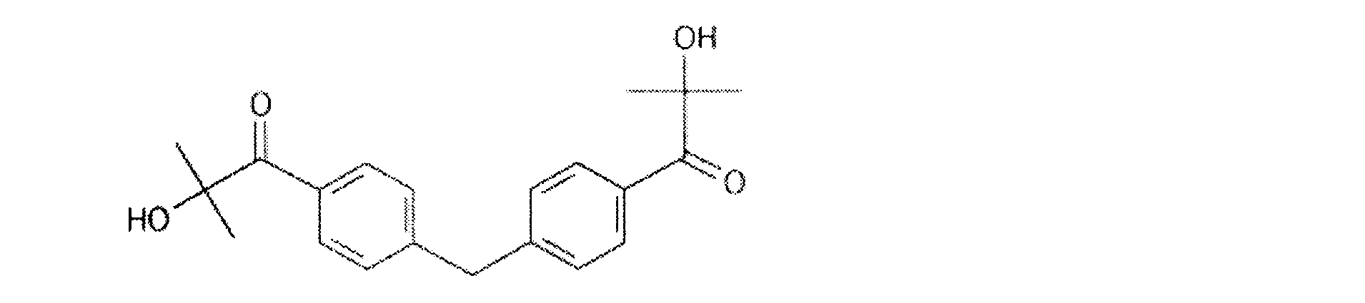
(6)名称:Omnirad369(登録商標)、IGM Resins B.V.社製(2-benzyl-2-(dimethylamino)-4′-morpholinobutyrophenone)
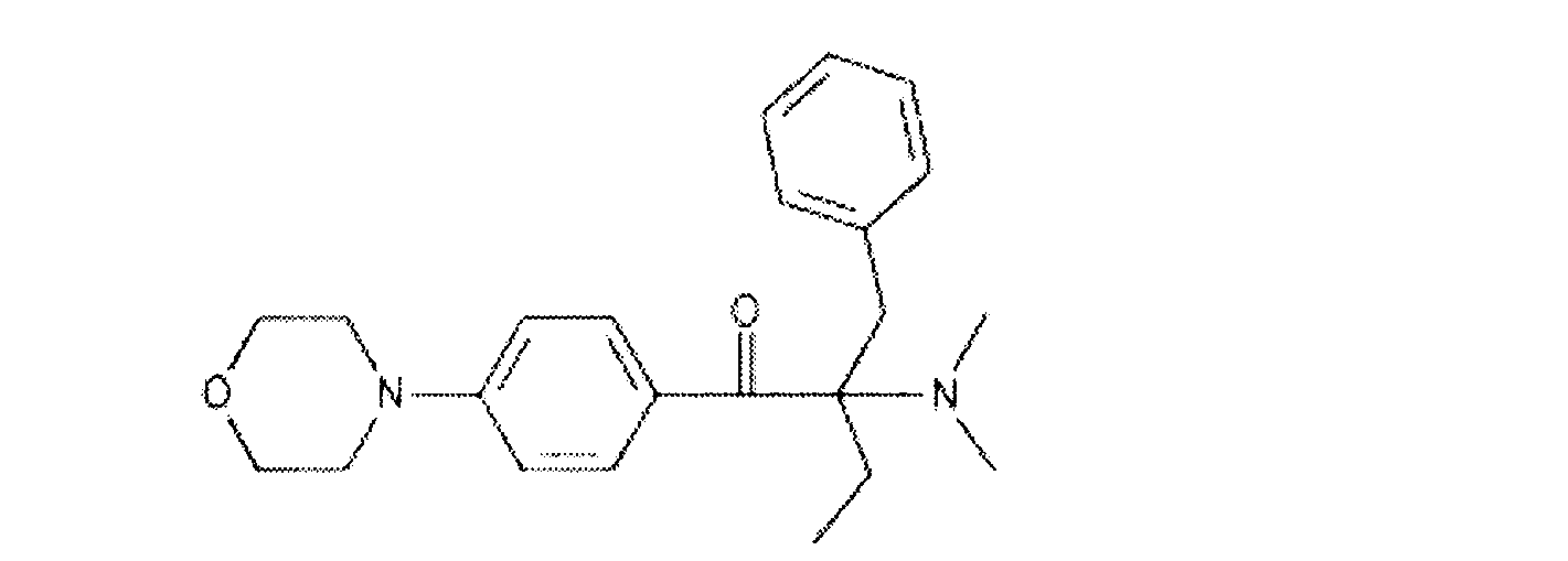
(7)名称:Omnirad379EG(登録商標)、IGM Resins B.V.社製(2-dimethylamino-2-(4-methyl-benzyl)-1-(4-morpholin-4-yl-phenyl)-butan-1-one)
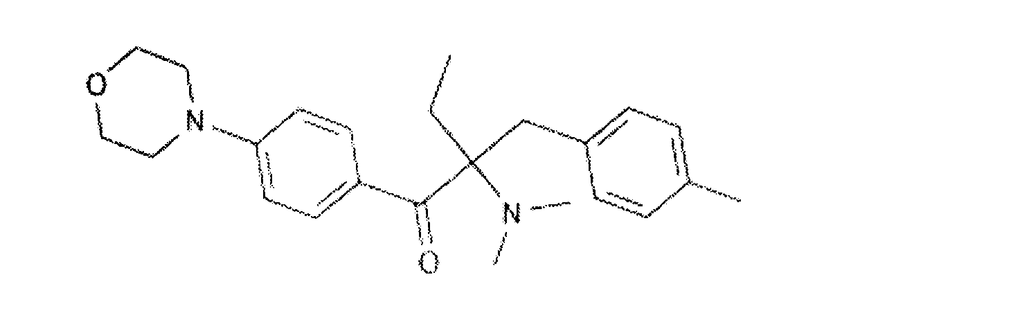
(8)名称:Omnirad MBF(登録商標)、IGM Resins B.V.社製(Methylbenzoylformate)
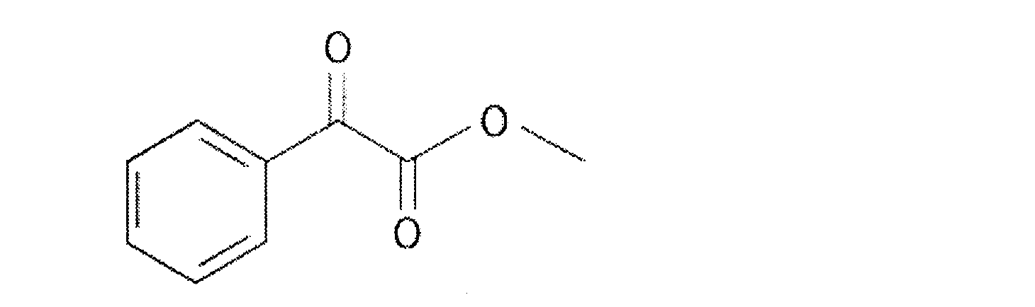
(9)名称:Irgacure OXE01(登録商標)、BASFジャパン株式会社製(1,2-Octanedione, 1-[4-(phenylthio) phenyl]-, 2-(o-benzoyloxime)

(10)名称:Irgacure OXE02(登録商標)、BASFジャパン株式会社製(Ethanone, 1-[9-ethyl-6-(2-methylbenzoyl)-9H-carbazol-3-yl]-, 1-(O-acetyloxime)

なお、本出願は、2019年3月4日出願の日本特許出願(特願2019-038939)に基づくものであり、その内容は本出願の中に参照として援用される。
65 フライアイレンズ
70,70A,70B 光源装置
71 第1のLEDアレイ
72 第1のLED素子
75,75A,75B 第2のLEDアレイ
76,76A,76B 第2のLED素子
78 LEDアレイ(光源装置)
80,80A,80B 光合成素子(ダイクロイックミラー)
81 ダイクロイック膜
83 端部
85 ダイクロイックミラー固定枠
180 光合成素子(ダイクロイックプリズム)
M マスク
PE 近接露光装置
W ワーク(基板)
L1 第1のLEDアレイの長さ
L2 第2のLEDアレイの長さ
70,70A,70B 光源装置
71 第1のLEDアレイ
72 第1のLED素子
75,75A,75B 第2のLEDアレイ
76,76A,76B 第2のLED素子
78 LEDアレイ(光源装置)
80,80A,80B 光合成素子(ダイクロイックミラー)
81 ダイクロイック膜
83 端部
85 ダイクロイックミラー固定枠
180 光合成素子(ダイクロイックプリズム)
M マスク
PE 近接露光装置
W ワーク(基板)
L1 第1のLEDアレイの長さ
L2 第2のLEDアレイの長さ
Claims (14)
- 第1のピーク波長の光を発光する複数の第1のLED素子を有する第1のLEDアレイと、
第1のピーク波長と異なる第2のピーク波長の光を発光する複数の第2のLED素子を有する第2のLEDアレイと、
該第1及び第2のLEDアレイの光を合成する光合成素子と、
前記光合成素子によって合成された光が入射されるフライアイレンズと、
を備える、露光用の光源装置であって、
前記光合成素子は、特定の波長帯域の光を透過させ、その他の波長帯域の光を反射させる2つのダイクロイック膜を備え、該2つのダイクロイック膜は、前記光合成素子から前記フライアイレンズに向かう光軸方向に対して傾斜し、且つ、前記フライアイレンズ側で密着するように略V字形に配置され、
前記第1のLEDアレイは、前記光軸方向において、前記光合成素子に対して前記フライアイレンズの反対側に配置され、
前記第2のLEDアレイは、前記光軸方向に対して交差して、前記光合成素子の側方に配置される、露光用の光源装置。 - 前記第1のLED素子と前記第2のLED素子のいずれか一方から照射される光のピーク波長は、360~380nmであり、
前記第1のLED素子と前記第2のLED素子のいずれか他方から照射される光のピーク波長は、300~355nm又は385~410nmであり、
前記第1のLED素子と前記第2のLED素子の各ピーク波長は、20nm以上離れている、請求項1に記載の露光用の光源装置。 - 前記光合成素子の側方に配置される前記第2のLEDアレイの長さは、
前記光合成素子に対して前記フライアイレンズの反対側に配置される前記第1のLEDアレイの長さより短い、請求項1又は2に記載の露光用の光源装置。 - 前記光合成素子は、2枚のダイクロイックミラーまたはダイクロイックプリズムである、請求項1~3のいずれか1項に記載の露光用の光源装置。
- 前記光合成素子は、前記ダイクロイック膜をそれぞれ有する2枚のダイクロイックミラーであって、
前記各ダイクロイックミラーの端部は、前記光軸方向と平行にカットされる、請求項1に記載の露光用の光源装置。 - 前記ダイクロイックミラーがそれぞれ固定され、前記2枚のダイクロイックミラーが密着する側において開放された2つのダイクロイックミラー固定枠をさらに備え、
前記ダイクロイックミラー固定枠の前記フライアイレンズ側の先端は、前記光軸方向と直角にカットされる、請求項5に記載の露光用の光源装置。 - 前記第2のLEDアレイは、前記光軸方向に対して直交する平面上に、90°間隔で交互に配置される、2種類の2つの第2のLEDアレイを有する、請求項1~6のいずれか1項に記載の露光用の光源装置。
- 請求項1~7のいずれか1項に記載の露光用の光源装置を有する照明装置と、
ワークを支持するワーク支持部と、
マスクを支持しるマスク支持部と、
を備え、前記照明装置から照射される光を、前記マスクを介して前記ワークに照射して前記マスクのパターンを前記ワークに転写する露光装置。 - 請求項8に記載の露光装置を用いて、前記照明装置から照射される光を、前記マスクを介して前記ワークに照射して前記マスクのパターンを前記ワークに転写する露光方法。
- 基板に設けられた感光材料の重合開始剤の感光波長に対応する、360~380nmの範囲に第1のピーク波長の光を発光する複数の第1のLED素子と、300~355nmの範囲に第2のピーク波長の光を発光する複数の第2のLED素子と、
を備え、
前記第1のLED素子の光と前記第2のLED素子の光が、混合してフライアイレンズに出射される、露光用の光源装置。 - 前記第1のLED素子及び前記第2のLED素子が混在して配置されるLEDアレイを備える、請求項10に記載の露光用の光源装置。
- 前記複数の第1のLED素子を有する第1のLEDアレイと、
前記複数の第2のLED素子を有する第2のLEDアレイと、
該第1及び第2のLEDアレイの光を合成する光合成素子と、
を備え、
前記光合成素子は、特定の波長帯域の光を透過させ、その他の波長帯域の光を反射させるダイクロイック膜を、前記光合成素子から前記フライアイレンズに向かう光軸方向に対して傾斜して配置し、
前記第1のLEDアレイと前記第2のLEDアレイのいずれか一方は、前記光軸方向において、前記光合成素子に対して前記フライアイレンズの反対側に配置され、
前記第1のLEDアレイと前記第2のLEDアレイのいずれか他方は、前記光軸方向に対して交差して、前記光合成素子の側方に配置される、請求項10に記載の露光用の光源装置。 - 請求項10~12のいずれか1項に記載の露光用の光源装置を有する照明装置と、
ワークを支持するワーク支持部と、
マスクを支持しるマスク支持部と、
を備え、前記照明装置から照射される光を、前記マスクを介して前記ワークに照射して前記マスクのパターンを前記ワークに転写する露光装置。 - 請求項13に記載の露光装置を用いて、前記照明装置から照射される光を、前記マスクを介して前記ワークに照射して前記マスクのパターンを前記ワークに転写する露光方法。
Priority Applications (3)
| Application Number | Priority Date | Filing Date | Title |
|---|---|---|---|
| KR1020217027927A KR20210134326A (ko) | 2019-03-04 | 2020-03-02 | 노광용 광원 장치, 노광 장치, 및 노광 방법 |
| CN202080018580.0A CN113544589A (zh) | 2019-03-04 | 2020-03-02 | 曝光用的光源装置、曝光装置及曝光方法 |
| JP2021504086A JPWO2020179740A1 (ja) | 2019-03-04 | 2020-03-02 |
Applications Claiming Priority (2)
| Application Number | Priority Date | Filing Date | Title |
|---|---|---|---|
| JP2019038939 | 2019-03-04 | ||
| JP2019-038939 | 2019-03-04 |
Publications (1)
| Publication Number | Publication Date |
|---|---|
| WO2020179740A1 true WO2020179740A1 (ja) | 2020-09-10 |
Family
ID=72338374
Family Applications (1)
| Application Number | Title | Priority Date | Filing Date |
|---|---|---|---|
| PCT/JP2020/008724 Ceased WO2020179740A1 (ja) | 2019-03-04 | 2020-03-02 | 露光用の光源装置、露光装置、及び露光方法 |
Country Status (5)
| Country | Link |
|---|---|
| JP (1) | JPWO2020179740A1 (ja) |
| KR (1) | KR20210134326A (ja) |
| CN (1) | CN113544589A (ja) |
| TW (1) | TW202040281A (ja) |
| WO (1) | WO2020179740A1 (ja) |
Families Citing this family (2)
| Publication number | Priority date | Publication date | Assignee | Title |
|---|---|---|---|---|
| KR102916425B1 (ko) * | 2020-07-07 | 2026-01-23 | 페닉스덴키가부시키가이샤 | 노광용 광원, 광조사 장치, 노광 장치 및 노광 방법 |
| CN115453825A (zh) * | 2022-08-12 | 2022-12-09 | 无锡旭电科技有限公司 | 一种uvled大功率阻焊制程平行光源系统 |
Citations (10)
| Publication number | Priority date | Publication date | Assignee | Title |
|---|---|---|---|---|
| JP2006184709A (ja) * | 2004-12-28 | 2006-07-13 | Nikon Corp | 結像光学系、露光装置及びマイクロデバイスの製造方法 |
| JP2010263218A (ja) * | 2009-05-07 | 2010-11-18 | Ultratech Inc | Led型紫外線照射器及び同照射器を用いたリソグラフィシステム |
| WO2012067246A1 (ja) * | 2010-11-19 | 2012-05-24 | Nskテクノロジー株式会社 | 近接露光装置及び近接露光方法 |
| JP2013162110A (ja) * | 2012-02-09 | 2013-08-19 | Topcon Corp | 露光装置 |
| JP2014207414A (ja) * | 2013-04-16 | 2014-10-30 | 株式会社オーク製作所 | 露光装置 |
| JP2015099247A (ja) * | 2013-11-19 | 2015-05-28 | Hoya株式会社 | フォトマスク及び該フォトマスクを用いた基板の製造方法 |
| JP2016071243A (ja) * | 2014-09-30 | 2016-05-09 | 富士フイルム株式会社 | 樹脂パターンの形成方法、パターンの形成方法、硬化膜、液晶表示装置、有機el表示装置、及び、タッチパネル表示装置 |
| JP2017161603A (ja) * | 2016-03-07 | 2017-09-14 | ウシオ電機株式会社 | 光源装置及びこれを備えた露光装置 |
| JP2017187545A (ja) * | 2016-04-01 | 2017-10-12 | シーシーエス株式会社 | 光照射装置 |
| WO2018211886A1 (ja) * | 2017-05-19 | 2018-11-22 | ソニー株式会社 | 投射型表示装置 |
Family Cites Families (1)
| Publication number | Priority date | Publication date | Assignee | Title |
|---|---|---|---|---|
| DE202016103819U1 (de) | 2016-07-14 | 2017-10-20 | Suss Microtec Lithography Gmbh | Lichtquellenanordnung für ein Belichtungssystem sowie Fotolithografie-Belichtungssystem |
-
2020
- 2020-03-02 JP JP2021504086A patent/JPWO2020179740A1/ja active Pending
- 2020-03-02 KR KR1020217027927A patent/KR20210134326A/ko not_active Withdrawn
- 2020-03-02 WO PCT/JP2020/008724 patent/WO2020179740A1/ja not_active Ceased
- 2020-03-02 CN CN202080018580.0A patent/CN113544589A/zh active Pending
- 2020-03-04 TW TW109107050A patent/TW202040281A/zh unknown
Patent Citations (10)
| Publication number | Priority date | Publication date | Assignee | Title |
|---|---|---|---|---|
| JP2006184709A (ja) * | 2004-12-28 | 2006-07-13 | Nikon Corp | 結像光学系、露光装置及びマイクロデバイスの製造方法 |
| JP2010263218A (ja) * | 2009-05-07 | 2010-11-18 | Ultratech Inc | Led型紫外線照射器及び同照射器を用いたリソグラフィシステム |
| WO2012067246A1 (ja) * | 2010-11-19 | 2012-05-24 | Nskテクノロジー株式会社 | 近接露光装置及び近接露光方法 |
| JP2013162110A (ja) * | 2012-02-09 | 2013-08-19 | Topcon Corp | 露光装置 |
| JP2014207414A (ja) * | 2013-04-16 | 2014-10-30 | 株式会社オーク製作所 | 露光装置 |
| JP2015099247A (ja) * | 2013-11-19 | 2015-05-28 | Hoya株式会社 | フォトマスク及び該フォトマスクを用いた基板の製造方法 |
| JP2016071243A (ja) * | 2014-09-30 | 2016-05-09 | 富士フイルム株式会社 | 樹脂パターンの形成方法、パターンの形成方法、硬化膜、液晶表示装置、有機el表示装置、及び、タッチパネル表示装置 |
| JP2017161603A (ja) * | 2016-03-07 | 2017-09-14 | ウシオ電機株式会社 | 光源装置及びこれを備えた露光装置 |
| JP2017187545A (ja) * | 2016-04-01 | 2017-10-12 | シーシーエス株式会社 | 光照射装置 |
| WO2018211886A1 (ja) * | 2017-05-19 | 2018-11-22 | ソニー株式会社 | 投射型表示装置 |
Also Published As
| Publication number | Publication date |
|---|---|
| JPWO2020179740A1 (ja) | 2020-09-10 |
| CN113544589A (zh) | 2021-10-22 |
| TW202040281A (zh) | 2020-11-01 |
| KR20210134326A (ko) | 2021-11-09 |
Similar Documents
| Publication | Publication Date | Title |
|---|---|---|
| CN100487561C (zh) | 图像显示装置 | |
| KR20190103210A (ko) | 3차원 물체를 성형하기 위해 액상 중합체의 광-경화를 위한 광 엔진을 사용하는 방법 및 장치 | |
| US20090046262A1 (en) | Exposure apparatus and exposure method | |
| CN103299243B (zh) | 接近式曝光装置以及接近式曝光方法 | |
| WO2021251090A1 (ja) | 露光用の光源装置、照明装置、露光装置、及び露光方法 | |
| KR20210134326A (ko) | 노광용 광원 장치, 노광 장치, 및 노광 방법 | |
| TWI276926B (en) | Light irradiating apparatus | |
| CN1516976A (zh) | 投影系统的光学装置 | |
| CN1881091A (zh) | 离轴投影光学系统及使用该系统的超紫外线光刻装置 | |
| JP2004354909A (ja) | 投影露光装置および投影露光方法 | |
| TW200844674A (en) | Reflection-deflection type projection optical system, projection optical apparatus, and scanning aligner | |
| CN101000409A (zh) | 一种可变倍率投影光学系统 | |
| WO2024221878A1 (zh) | 光机系统、投影方法和光固化打印机 | |
| KR101607578B1 (ko) | 노광 장치 및 마스크 얼라이너 | |
| CN105209976B (zh) | 曝光装置和照明单元 | |
| ATE501454T1 (de) | Optisches projektionssystem und belichtungsvorrichtung damit | |
| TWI876438B (zh) | 光源單元、照明單元、曝光裝置、及曝光方法 | |
| JP7806909B2 (ja) | 照明ユニット、露光装置、及び露光方法 | |
| CN220004778U (zh) | 紫外光照结构及紫外光固化设备 | |
| KR101838774B1 (ko) | 투영 광학계와 투영 노광 장치 | |
| JP5571967B2 (ja) | 投影光学系と投影露光装置 | |
| JP2003185920A (ja) | 結像光学系及び投影露光装置 | |
| CN114228147A (zh) | 一种多光谱合成紫外光源模组及dlp面投影系统 | |
| WO2025079172A1 (ja) | 光源ユニット、照明ユニット、露光装置、及び露光方法 | |
| WO2024038537A1 (ja) | 光源ユニット、照明ユニット、露光装置、及び露光方法 |
Legal Events
| Date | Code | Title | Description |
|---|---|---|---|
| 121 | Ep: the epo has been informed by wipo that ep was designated in this application |
Ref document number: 20767246 Country of ref document: EP Kind code of ref document: A1 |
|
| ENP | Entry into the national phase |
Ref document number: 2021504086 Country of ref document: JP Kind code of ref document: A |
|
| NENP | Non-entry into the national phase |
Ref country code: DE |
|
| 122 | Ep: pct application non-entry in european phase |
Ref document number: 20767246 Country of ref document: EP Kind code of ref document: A1 |