WO2020179056A1 - 半導体結晶薄膜の製造方法、及びレーザアニールシステム - Google Patents
半導体結晶薄膜の製造方法、及びレーザアニールシステム Download PDFInfo
- Publication number
- WO2020179056A1 WO2020179056A1 PCT/JP2019/009078 JP2019009078W WO2020179056A1 WO 2020179056 A1 WO2020179056 A1 WO 2020179056A1 JP 2019009078 W JP2019009078 W JP 2019009078W WO 2020179056 A1 WO2020179056 A1 WO 2020179056A1
- Authority
- WO
- WIPO (PCT)
- Prior art keywords
- laser
- laser light
- pulse
- irradiation
- laser annealing
- Prior art date
- Legal status (The legal status is an assumption and is not a legal conclusion. Google has not performed a legal analysis and makes no representation as to the accuracy of the status listed.)
- Ceased
Links
Images













Classifications
-
- H—ELECTRICITY
- H10—SEMICONDUCTOR DEVICES; ELECTRIC SOLID-STATE DEVICES NOT OTHERWISE PROVIDED FOR
- H10P—GENERIC PROCESSES OR APPARATUS FOR THE MANUFACTURE OR TREATMENT OF DEVICES COVERED BY CLASS H10
- H10P72/00—Handling or holding of wafers, substrates or devices during manufacture or treatment thereof
- H10P72/04—Apparatus for manufacture or treatment
- H10P72/0431—Apparatus for thermal treatment
- H10P72/0436—Apparatus for thermal treatment mainly by radiation
-
- H—ELECTRICITY
- H01—ELECTRIC ELEMENTS
- H01S—DEVICES USING THE PROCESS OF LIGHT AMPLIFICATION BY STIMULATED EMISSION OF RADIATION [LASER] TO AMPLIFY OR GENERATE LIGHT; DEVICES USING STIMULATED EMISSION OF ELECTROMAGNETIC RADIATION IN WAVE RANGES OTHER THAN OPTICAL
- H01S3/00—Lasers, i.e. devices using stimulated emission of electromagnetic radiation in the infrared, visible or ultraviolet wave range
- H01S3/005—Optical devices external to the laser cavity, specially adapted for lasers, e.g. for homogenisation of the beam or for manipulating laser pulses, e.g. pulse shaping
-
- H—ELECTRICITY
- H01—ELECTRIC ELEMENTS
- H01S—DEVICES USING THE PROCESS OF LIGHT AMPLIFICATION BY STIMULATED EMISSION OF RADIATION [LASER] TO AMPLIFY OR GENERATE LIGHT; DEVICES USING STIMULATED EMISSION OF ELECTROMAGNETIC RADIATION IN WAVE RANGES OTHER THAN OPTICAL
- H01S3/00—Lasers, i.e. devices using stimulated emission of electromagnetic radiation in the infrared, visible or ultraviolet wave range
- H01S3/005—Optical devices external to the laser cavity, specially adapted for lasers, e.g. for homogenisation of the beam or for manipulating laser pulses, e.g. pulse shaping
- H01S3/0057—Temporal shaping, e.g. pulse compression, frequency chirping
-
- H—ELECTRICITY
- H01—ELECTRIC ELEMENTS
- H01S—DEVICES USING THE PROCESS OF LIGHT AMPLIFICATION BY STIMULATED EMISSION OF RADIATION [LASER] TO AMPLIFY OR GENERATE LIGHT; DEVICES USING STIMULATED EMISSION OF ELECTROMAGNETIC RADIATION IN WAVE RANGES OTHER THAN OPTICAL
- H01S3/00—Lasers, i.e. devices using stimulated emission of electromagnetic radiation in the infrared, visible or ultraviolet wave range
- H01S3/23—Arrangements of two or more lasers not provided for in groups H01S3/02 - H01S3/22, e.g. tandem arrangements of separate active media
- H01S3/2366—Arrangements of two or more lasers not provided for in groups H01S3/02 - H01S3/22, e.g. tandem arrangements of separate active media comprising a gas as the active medium
-
- H—ELECTRICITY
- H10—SEMICONDUCTOR DEVICES; ELECTRIC SOLID-STATE DEVICES NOT OTHERWISE PROVIDED FOR
- H10D—INORGANIC ELECTRIC SEMICONDUCTOR DEVICES
- H10D30/00—Field-effect transistors [FET]
- H10D30/60—Insulated-gate field-effect transistors [IGFET]
- H10D30/67—Thin-film transistors [TFT]
-
- H—ELECTRICITY
- H10—SEMICONDUCTOR DEVICES; ELECTRIC SOLID-STATE DEVICES NOT OTHERWISE PROVIDED FOR
- H10P—GENERIC PROCESSES OR APPARATUS FOR THE MANUFACTURE OR TREATMENT OF DEVICES COVERED BY CLASS H10
- H10P14/00—Formation of materials, e.g. in the shape of layers or pillars
- H10P14/20—Formation of materials, e.g. in the shape of layers or pillars of semiconductor materials
- H10P14/34—Deposited materials, e.g. layers
- H10P14/3402—Deposited materials, e.g. layers characterised by the chemical composition
- H10P14/3404—Deposited materials, e.g. layers characterised by the chemical composition being Group IVA materials
- H10P14/3411—Silicon, silicon germanium or germanium
-
- H—ELECTRICITY
- H10—SEMICONDUCTOR DEVICES; ELECTRIC SOLID-STATE DEVICES NOT OTHERWISE PROVIDED FOR
- H10P—GENERIC PROCESSES OR APPARATUS FOR THE MANUFACTURE OR TREATMENT OF DEVICES COVERED BY CLASS H10
- H10P14/00—Formation of materials, e.g. in the shape of layers or pillars
- H10P14/20—Formation of materials, e.g. in the shape of layers or pillars of semiconductor materials
- H10P14/34—Deposited materials, e.g. layers
- H10P14/3451—Structure
- H10P14/3452—Microstructure
- H10P14/3454—Amorphous
-
- H—ELECTRICITY
- H10—SEMICONDUCTOR DEVICES; ELECTRIC SOLID-STATE DEVICES NOT OTHERWISE PROVIDED FOR
- H10P—GENERIC PROCESSES OR APPARATUS FOR THE MANUFACTURE OR TREATMENT OF DEVICES COVERED BY CLASS H10
- H10P34/00—Irradiation with electromagnetic or particle radiation of wafers, substrates or parts of devices
- H10P34/40—Irradiation with electromagnetic or particle radiation of wafers, substrates or parts of devices with high-energy radiation
- H10P34/42—Irradiation with electromagnetic or particle radiation of wafers, substrates or parts of devices with high-energy radiation with electromagnetic radiation, e.g. laser annealing
-
- H—ELECTRICITY
- H01—ELECTRIC ELEMENTS
- H01S—DEVICES USING THE PROCESS OF LIGHT AMPLIFICATION BY STIMULATED EMISSION OF RADIATION [LASER] TO AMPLIFY OR GENERATE LIGHT; DEVICES USING STIMULATED EMISSION OF ELECTROMAGNETIC RADIATION IN WAVE RANGES OTHER THAN OPTICAL
- H01S3/00—Lasers, i.e. devices using stimulated emission of electromagnetic radiation in the infrared, visible or ultraviolet wave range
- H01S3/09—Processes or apparatus for excitation, e.g. pumping
- H01S3/097—Processes or apparatus for excitation, e.g. pumping by gas discharge of a gas laser
- H01S3/0971—Processes or apparatus for excitation, e.g. pumping by gas discharge of a gas laser transversely excited
-
- H—ELECTRICITY
- H01—ELECTRIC ELEMENTS
- H01S—DEVICES USING THE PROCESS OF LIGHT AMPLIFICATION BY STIMULATED EMISSION OF RADIATION [LASER] TO AMPLIFY OR GENERATE LIGHT; DEVICES USING STIMULATED EMISSION OF ELECTROMAGNETIC RADIATION IN WAVE RANGES OTHER THAN OPTICAL
- H01S3/00—Lasers, i.e. devices using stimulated emission of electromagnetic radiation in the infrared, visible or ultraviolet wave range
- H01S3/14—Lasers, i.e. devices using stimulated emission of electromagnetic radiation in the infrared, visible or ultraviolet wave range characterised by the material used as the active medium
- H01S3/22—Gases
- H01S3/223—Gases the active gas being polyatomic, i.e. containing two or more atoms
- H01S3/225—Gases the active gas being polyatomic, i.e. containing two or more atoms comprising an excimer or exciplex
-
- H—ELECTRICITY
- H01—ELECTRIC ELEMENTS
- H01S—DEVICES USING THE PROCESS OF LIGHT AMPLIFICATION BY STIMULATED EMISSION OF RADIATION [LASER] TO AMPLIFY OR GENERATE LIGHT; DEVICES USING STIMULATED EMISSION OF ELECTROMAGNETIC RADIATION IN WAVE RANGES OTHER THAN OPTICAL
- H01S3/00—Lasers, i.e. devices using stimulated emission of electromagnetic radiation in the infrared, visible or ultraviolet wave range
- H01S3/23—Arrangements of two or more lasers not provided for in groups H01S3/02 - H01S3/22, e.g. tandem arrangements of separate active media
- H01S3/2383—Parallel arrangements
-
- H—ELECTRICITY
- H10—SEMICONDUCTOR DEVICES; ELECTRIC SOLID-STATE DEVICES NOT OTHERWISE PROVIDED FOR
- H10P—GENERIC PROCESSES OR APPARATUS FOR THE MANUFACTURE OR TREATMENT OF DEVICES COVERED BY CLASS H10
- H10P14/00—Formation of materials, e.g. in the shape of layers or pillars
- H10P14/20—Formation of materials, e.g. in the shape of layers or pillars of semiconductor materials
- H10P14/34—Deposited materials, e.g. layers
- H10P14/3451—Structure
-
- H—ELECTRICITY
- H10—SEMICONDUCTOR DEVICES; ELECTRIC SOLID-STATE DEVICES NOT OTHERWISE PROVIDED FOR
- H10P—GENERIC PROCESSES OR APPARATUS FOR THE MANUFACTURE OR TREATMENT OF DEVICES COVERED BY CLASS H10
- H10P14/00—Formation of materials, e.g. in the shape of layers or pillars
- H10P14/20—Formation of materials, e.g. in the shape of layers or pillars of semiconductor materials
- H10P14/38—Formation of materials, e.g. in the shape of layers or pillars of semiconductor materials characterised by treatments done after the formation of the materials
- H10P14/3802—Crystallisation or recrystallisation of non-monocrystalline semiconductor materials, e.g. regrowth
- H10P14/3808—Crystallisation or recrystallisation of non-monocrystalline semiconductor materials, e.g. regrowth using laser beams
- H10P14/381—Beam shaping, e.g. using a mask
-
- H—ELECTRICITY
- H10—SEMICONDUCTOR DEVICES; ELECTRIC SOLID-STATE DEVICES NOT OTHERWISE PROVIDED FOR
- H10P—GENERIC PROCESSES OR APPARATUS FOR THE MANUFACTURE OR TREATMENT OF DEVICES COVERED BY CLASS H10
- H10P14/00—Formation of materials, e.g. in the shape of layers or pillars
- H10P14/20—Formation of materials, e.g. in the shape of layers or pillars of semiconductor materials
- H10P14/38—Formation of materials, e.g. in the shape of layers or pillars of semiconductor materials characterised by treatments done after the formation of the materials
- H10P14/3802—Crystallisation or recrystallisation of non-monocrystalline semiconductor materials, e.g. regrowth
- H10P14/3808—Crystallisation or recrystallisation of non-monocrystalline semiconductor materials, e.g. regrowth using laser beams
- H10P14/3816—Pulsed laser beam
-
- H—ELECTRICITY
- H10—SEMICONDUCTOR DEVICES; ELECTRIC SOLID-STATE DEVICES NOT OTHERWISE PROVIDED FOR
- H10P—GENERIC PROCESSES OR APPARATUS FOR THE MANUFACTURE OR TREATMENT OF DEVICES COVERED BY CLASS H10
- H10P14/00—Formation of materials, e.g. in the shape of layers or pillars
- H10P14/20—Formation of materials, e.g. in the shape of layers or pillars of semiconductor materials
- H10P14/38—Formation of materials, e.g. in the shape of layers or pillars of semiconductor materials characterised by treatments done after the formation of the materials
- H10P14/3802—Crystallisation or recrystallisation of non-monocrystalline semiconductor materials, e.g. regrowth
- H10P14/382—Scanning of a beam
Definitions
- the present disclosure relates to a method for manufacturing a semiconductor crystal thin film and a laser annealing system.
- a thin film transistor (TFT: Thin Film Transistor) is used as a driving element of a flat panel display using a glass substrate.
- TFT Thin Film Transistor
- Polycrystalline silicon, IGZO (Indium gallium zinc oxide), and the like are used for the semiconductor thin film which is the channel material of the TFT.
- Polycrystalline silicon and IGZO have higher carrier mobility than amorphous silicon and are superior in on/off characteristics of transistors.
- semiconductor thin films are also expected to be applied to 3D-ICs that realize more sophisticated devices.
- the 3D-IC is realized by forming active elements such as a sensor, an amplifier circuit, and a CMOS circuit on the uppermost layer of the integrated circuit device. Therefore, a technique for manufacturing a higher quality semiconductor thin film is required.
- a glass substrate used for a display is required to have a process temperature of 400° C.
- an integrated circuit is required to have a process temperature of 400° C.
- a plastic substrate PET is required to have a process temperature of 200° C. or lower.
- Laser annealing is used as a technique to crystallize the underlying substrate of a semiconductor thin film without heat damage.
- pulsed ultraviolet laser light absorbed by the upper semiconductor thin film is used in order to suppress damage to the substrate due to thermal diffusion.
- the semiconductor thin film is silicon
- a 351 nm wavelength XeF excimer laser, a 308 nm wavelength XeCl excimer laser, a 248 nm wavelength KrF excimer laser, etc. are used.
- These gas lasers in the ultraviolet region have the characteristics that the coherence of laser light is lower than that of solid-state lasers, the energy uniformity on the laser light irradiation surface is excellent, and a wide region can be annealed uniformly with high pulse energy.
- a method of manufacturing a semiconductor crystal thin film according to one aspect of the present disclosure includes irradiating an amorphous semiconductor with a first pulsed laser beam having a first pulse time width to polycrystallize the amorphous semiconductor.
- the semiconductor crystal Reducing the height of the ridge of the.
- a laser annealing system includes a first pulse laser beam having a first pulse time width and a second pulse laser having a second pulse time width shorter than the first pulse time width.
- the laser annealing device includes a laser system that outputs light, and a laser annealing device that irradiates the irradiation target with the first pulsed laser light and the second pulsed laser light.
- Optical system that guides the pulsed laser light to the object to be irradiated, a moving mechanism that relatively moves the irradiation positions of the first pulsed laser light and the second pulsed laser light to the object to be irradiated, and a first pulsed laser
- the laser system is controlled so that the irradiation object is irradiated with the first pulsed laser light and then the second pulsed laser light is irradiated to a region of the irradiation object which is irradiated with the first pulsed laser light.
- FIG. 1 is an explanatory diagram of a pulse time width of laser light.
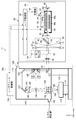
- FIG. 2 schematically illustrates the configuration of an exemplary laser annealing system.
- FIG. 3 is a plan view showing an example of the relationship between the mask pattern and the line beam that illuminates the mask.
- FIG. 4 is a plan view showing an example of scan irradiation of a line beam on an object to be irradiated.
- FIG. 5 is an enlarged view of a portion surrounded by a broken line circle in FIG.
- FIG. 6 is a flowchart showing an example of the operation of the laser annealing system.
- FIG. 1 is an explanatory diagram of a pulse time width of laser light.
- FIG. 2 schematically illustrates the configuration of an exemplary laser annealing system.
- FIG. 3 is a plan view showing an example of the relationship between the mask pattern and the line beam that illuminates the mask.
- FIG. 4 is a plan view showing an example of scan irradiation of a
- FIG. 7 is a flowchart showing an example of a subroutine applied to step S12 of FIG.
- FIG. 8 is a flowchart showing an example of a subroutine applied to step S14 of FIG.
- FIG. 9 is a flowchart showing an example of a subroutine applied to step S20 of FIG.
- FIG. 10 is a flowchart showing an example of a subroutine applied to step S22 of FIG.
- FIG. 11 is a schematic diagram of a semiconductor crystal thin film manufacturing process by laser annealing.
- FIG. 12 is a schematic view schematically showing a manufacturing process of the semiconductor crystal thin film according to the first embodiment.
- FIG. 13 is a chart showing irradiation conditions of the laser beam applied at the time of the test.
- FIG. 14 is a graph showing an example of a pulse waveform of laser light.
- FIG. 15 shows a configuration example of the optical pulse stretcher system.
- FIG. 16 shows an example of a mask pattern and crystal growth.
- FIG. 17 schematically shows the configuration of the laser annealing system according to the first embodiment.
- FIG. 18 is a plan view showing an example of beam scan irradiation during ridge flattening in the first embodiment.
- FIG. 19 is a flowchart showing an example of the operation of the laser annealing system according to the first embodiment.
- FIG. 20 is a flowchart showing an example of a subroutine applied to step S13 of FIG.
- FIG. 21 is a flowchart showing an example of a subroutine applied to step S21 of FIG.
- FIG. 20 is a flowchart showing an example of a subroutine applied to step S13 of FIG.
- FIG. 21 is a flowchart showing an example of a subroutine applied to step S21 of FIG.
- FIG. 22 is a flowchart showing an example of a subroutine applied to step S24 of FIG.
- FIG. 23 is a flowchart showing an example of the subroutine applied to step S26 of FIG.
- FIG. 24 is a flowchart showing an example of the subroutine applied to step S28 of FIG.
- FIG. 25 schematically shows the configuration of the laser annealing system according to the second embodiment.
- FIG. 26 schematically shows the configuration of the laser annealing system according to the third embodiment.
- FIG. 27 is a plan view showing an example of the relationship between the mask pattern and the line beam that illuminates the mask.
- FIG. 28 is a plan view showing an example of scan irradiation of a line beam on an object to be irradiated.
- FIG. 29 schematically shows the configuration of the laser annealing system according to the fourth embodiment.
- FIG. 30 schematically shows the configuration of the laser annealing system according to the fifth embodiment.
- FIG. 31 schematically shows the configuration of the laser annealing system according to the sixth embodiment.
- FIG. 32 shows an example of a mask and a beam irradiation region for the mask.
- FIG. 33 is an enlarged view showing an example of a fine pattern formed in the pattern area of the mask.
- FIG. 34 is an explanatory diagram of the operation of the laser annealing system according to the sixth embodiment.
- FIG. 35 schematically shows the configuration of the laser annealing system according to the seventh embodiment.
- FIG. 36 schematically shows the configuration of the laser annealing system according to the eighth embodiment.
- Embodiment 5 8.1 Configuration 8.2 Operation 8.3 Action/Effect 8.4 Modification 9
- Embodiment 6 9.1 Configuration 9.2 Operation 9.3 Action/Effect 9.4 Modified Example 10.
- Embodiment 7 10.1 Configuration 10.2 Operation 10.3 Action/Effect 10.4 Modification 11.
- Embodiment 8 11.1 Configuration 11.2 Operation 11.3 Action/Effect 11.4 Modified Example 12.
- FIG. 1 is an explanatory diagram of a pulse time width of laser light.
- the vertical axis of FIG. 1 is the light intensity I [a. u. ]
- the horizontal axis is time t [ns].
- Light intensity I [a. u. ] Is a value normalized with the peak value (maximum light intensity value) of the light intensity waveform being 1.
- the pulse time width ⁇ T 50% can be used as one of the indexes of the pulse time width of the laser light.
- the pulse time width ⁇ T 50% refers to the full width of time at the 50% value of the maximum light intensity value, as shown in FIG.
- TIS pulse time width ⁇ T TIS can be used as one of other indices of the pulse time width of the laser light.
- the TIS pulse time width ⁇ T TIS is defined by the following equation (1).
- I(t) is the light intensity at time t.
- FIG. 2 schematically illustrates the configuration of an exemplary laser annealing system.
- the laser annealing system 10 includes a laser device 20, an optical path tube 25, and a laser annealing device 100.
- the optical path tube 25 is arranged on the optical path of the laser light between the laser light emitting port of the laser device 20 and the laser light incident port of the laser annealing device 100.
- the laser device 20 is a laser device that outputs pulsed laser light of ultraviolet rays.
- the laser device 20 may be a discharge excitation laser device using F 2 , ArF, XeCl, or XeF as a laser medium.
- the laser device 20 includes a master oscillator (MO: Master Oscillator) 30, an optical pulse stretcher (OPS) system 32, a monitor module 34, a shutter 36, and a laser controller 38.
- MO Master Oscillator
- OPS optical pulse stretcher
- the master oscillator 30 includes a chamber 40, an optical resonator 42, a charger 44, and a pulse power module (PPM) 46.
- PPM pulse power module
- the excimer laser gas may be a mixed gas containing a rare gas such as Ar, Kr, or Xe, a halogen gas such as F 2 or Cl 2, and a buffer gas such as He or Ne.
- a rare gas such as Ar, Kr, or Xe
- a halogen gas such as F 2 or Cl 2
- a buffer gas such as He or Ne.
- the chamber 40 includes a pair of electrodes 48a and 48b and windows 50 and 52.
- the pair of electrodes 48a and 48b are arranged in the chamber 40.
- the electrode 48a is supported by the insulating member 54.
- the electrode 48 a is connected to the PPM 46 via the conductive portion 56 embedded in the feedthrough of the insulating member 54.
- the electrode 48b is supported by a return plate (not shown), and the return plate is connected to the inner surface of the chamber 40 by using a wiring (not shown).
- the PPM 46 includes a switch 47, a step-up transformer and a magnetic compression circuit, none of which are shown.
- the PPM 46 is connected to the charger 44.
- the charger 44 is a DC power supply device that charges a charging capacitor (not shown) in the PPM 46 with a predetermined voltage.
- the optical resonator 42 includes a rear mirror 60 and an output coupling mirror 62.
- the rear mirror 60 has a flat substrate coated with a highly reflective film.
- the output coupling mirror 62 has a planar substrate coated with a partial reflection film.
- the chamber 40 is arranged on the optical path of the optical resonator 42.
- the OPS system 32 is arranged on the optical path between the master oscillator 30 and the monitor module 34.
- the OPS system 32 includes an optical pulse stretcher (OPS) 33 that delays a portion of the incident light to stretch the time width of the pulsed laser light.
- OPS optical pulse stretcher
- the OPS 33 includes a beam splitter 70 and concave mirrors 71 to 74.
- the beam splitter 70 is arranged on the optical path between the master oscillator 30 and the monitor module 34.
- the beam splitter 70 is coated with a film that partially reflects a part of the incident pulsed laser light.
- the concave mirrors 71 to 74 have the same focal length, and the beams of the pulsed laser light reflected from the beam splitter 70 are highly reflected by the four concave mirrors 71 to 74 and are incident on the beam splitter 70 again. Arranged so that the beam is transferred at.
- the monitor module 34 includes a beam splitter 76 and an optical sensor 77.
- the shutter 36 is arranged on the optical path of the pulsed laser light output from the monitor module 34.
- the optical path of the pulsed laser light may be sealed by a casing (not shown) and the optical path tube 25, and may be purged with N 2 gas or the like.
- the laser annealing apparatus 100 includes an irradiation optical system 110, a frame 170, an XYZ axis stage 172, a table 174, and a laser annealing controller 180.
- the irradiated object 190 is fixed on the table 174.
- the irradiation optical system 110 includes high-reflection mirrors 121 to 123, an attenuator 130, an illumination optical system 140, a mask 148, a projection optical system 150, a window 160, and a housing 164.
- the high-reflection mirror 121 is arranged so that the laser light that has passed through the optical path tube 25 passes through the attenuator 130 and is incident on the high-reflection mirror 122.
- the attenuator 130 is arranged on the optical path between the high reflection mirror 121 and the high reflection mirror 122.
- the attenuator 130 includes two partial reflection mirrors 131 and 132, and rotating stages 135 and 136 that change the incident angle of the partial reflection mirrors 131 and 132, respectively.
- the high-reflection mirror 122 is arranged so that the laser light passing through the attenuator 130 enters the high-reflection mirror 123.
- the high-reflection mirror 123 is arranged so that the incident pulsed laser light is incident on the fly-eye lens 145 of the illumination optical system 140.
- the illumination optical system 140 includes a fly-eye lens 145 and a condenser lens 146.
- the illumination optical system 140 is an optical system for uniformly illuminating a predetermined illumination area on the mask 148, and is arranged so as to perform Koehler illumination on the mask 148 with a rectangular beam.
- the beam width of the rectangular beam with which the mask 148 is irradiated in the X-axis direction is Bmx
- the beam width in the Y-axis direction is Bmy.
- a rectangular beam satisfying Bmx ⁇ Bmy that is, a rectangular beam having the Y-axis direction as the major axis direction.
- a rectangular beam is referred to as a "line beam”.
- the fly-eye lens 145 is arranged, for example, so that the focal plane of the fly-eye lens 145 and the front focal plane of the condenser lens 146 coincide with each other, and the condenser lens 146 is located at the rear focal plane of the condenser lens 146 and the mask 148. Are arranged so that and match.
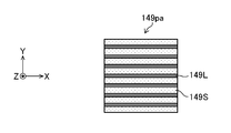
- the mask 148 is, for example, a mask in which a pattern of a metal or dielectric multilayer film is formed on a synthetic quartz substrate that transmits ultraviolet light. For example, a line-and-space pattern is formed on the mask 148 (see FIG. 3).
- the projection optical system 150 is arranged so that the image of the mask 148 is formed on the surface of the irradiation target 190 via the window 160.
- the projection optical system 150 is a combination lens of a plurality of lenses 152, and may be a reduction projection optical system.
- the window 160 is arranged on the optical path between the projection optical system 150 and the irradiation target 190.
- the window 160 is arranged in a hole provided in the housing 164 via an O-ring (not shown) or the like.
- the window 160 is a CaF 2 crystal or synthetic quartz substrate that transmits excimer laser light, and both surfaces may be coated with an antireflection film.
- the housing 164 is provided with an inlet 166 and an outlet 168 for nitrogen (N 2 ) gas.
- the housing 164 may be sealed via an O-ring or the like (not shown) so as to suppress entry of outside air into the housing 164.
- the N 2 gas inlet 166 is connected to an N 2 gas supply source (not shown).
- the irradiation optical system 110 and the XYZ axis stage 172 are fixed to the frame 170.
- the XYZ axis stage 172 is an electric stage that relatively moves the irradiation position of the pulsed laser light with respect to the irradiation object 190.
- the table 174 is fixed on the XYZ axis stage 172.
- the irradiation object 190 is fixed on the table 174.
- the irradiated object 190 is, for example, a substrate in which amorphous silicon is coated on a glass substrate.
- a silicon thin film will be described here as an example, the semiconductor thin film may be at least one of Si, Ge, SiGe, and GeSn.
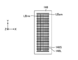
- FIG. 3 is a plan view showing an example of the relationship between the pattern of the mask 148 and the line beam LBm that illuminates the mask 148.
- the pattern of the mask 148 is, for example, a line-and-space pattern in which line portions 148L that are light shielding portions and space portions 148S that are light passing portions (non-light shielding portions) are alternately arranged.
- the short-axis direction (X-axis direction) of the line beam LBm that uniformly illuminates the mask 148 is parallel to the line direction of the line portion 148L, and a plurality of line portions 148L are formed in the long-axis direction (Y-axis direction) of the line beam LBm. Arranged at predetermined intervals.
- the laser light applied to the irradiation object 190 via the mask 148 is a beam group including a pattern corresponding to the image of the pattern of the mask 148. Since the pattern of the laser light with which the irradiation target 190 is irradiated through the mask 148 is substantially rectangular as a whole including the light shielding portion by the mask 148, the laser beam with which the irradiation target 190 is irradiated is also referred to as “line beam”. Is called.
- the line beam satisfies Bx ⁇ By here (see FIG. 4).
- the laser annealing control unit 180 reads the irradiation condition parameters during laser annealing. Specifically, each data of the fluence Fa on the irradiated object 190 when performing laser annealing, the number of irradiation pulses Na, and the repetition frequency fa is read.
- the various data and signals such as the target pulse energy Et are transmitted and received between the laser annealing control unit 180 and the laser control unit 38.
- the laser annealing control unit 180 causes the laser device 20 to perform adjustment oscillation.
- the laser control unit 38 receives the data of the target pulse energy Et from the laser annealing control unit 180.
- the laser control unit 38 Upon receiving the data of the target pulse energy Et, the laser control unit 38 closes the shutter 78 and controls the charger 44 so that the target pulse energy Et is achieved.
- the laser control unit 38 generates an internal trigger signal by an internal trigger generation unit (not shown), and the internal trigger signal is input to the switch 47 of the PPM 46. As a result, the master oscillator 30 spontaneously oscillates.
- the pulse laser light output from the master oscillator 30 is stretched in the time width of the pulse laser light by the OPS system 32.
- the pulsed laser light emitted from the OPS system 32 is sampled by the beam splitter 76 of the monitor module 34, and the pulse energy E is measured.
- the laser control unit 38 controls the charging voltage of the charger 44 so that the difference ⁇ E between the pulse energy E and the target pulse energy Et approaches 0.
- the laser control unit 38 transmits an external trigger OK signal to the laser annealing control unit 180 and opens the shutter 78.
- the laser annealing control unit 180 receives an external trigger OK signal from the laser control unit 38.
- the laser annealing control unit 180 controls the X axis and the Y axis of the XYZ axis stage 172 so that the position where the image of the mask 148 is transferred by the projection optical system 150 becomes the initial position.
- the laser annealing control unit 180 controls the Z axis of the XYZ axis stage 172 so that the image of the mask 148 is imaged at the position of the surface of the irradiation object 190.
- the laser annealing control unit 180 calculates the transmittance T of the attenuator 130 so that the fluence at the surface position of the irradiation object 190 (that is, the position of the image of the mask 148) becomes the target fluence Fa.
- the laser annealing control unit 180 controls the incident angles of the two partial reflection mirrors 131 and 132 by the rotary stages 135 and 136 so that the transmittance of the attenuator 130 becomes T.
- the laser annealing control unit 180 calculates the moving speed Vx of the XYZ axis stage 172 so that the irradiation pulse number is Na when the line beam width Bx on the irradiation object 190 is the repetition frequency fa.
- the laser annealing control unit 180 controls the XYZ axis stage 172 so that the table 174 moves in a uniform linear motion at a speed of Vx in the X axis direction.
- the line beam linearly moves on the surface of the irradiation object 190 in the direction opposite to the moving direction of the table 174 at a velocity of Vx.
- the laser annealing control unit 180 transmits the light emission trigger signal Tr having the repetition frequency fa to the laser control unit 38.
- the pulse laser light is output from the master oscillator 30 in synchronization with the light emission trigger signal Tr, and the pulse laser light transmitted through the beam splitter 76 of the monitor module 34 enters the laser annealing apparatus 100 via the optical path tube 25. To do.
- the pulsed laser light incident on the laser annealing device 100 is reflected by the high reflection mirror 121, dimmed through the attenuator 130, and reflected by the high reflection mirror 122.
- the pulsed laser light highly reflected by the high-reflection mirrors 122 and 123 is spatially equalized in light intensity by the illumination optical system 140, and is incident on the mask 148 as a line beam LBm.
- the pulsed laser light transmitted through the mask 148 is projected by the projection optical system 150 onto the surface of the irradiation object 190.
- the pulsed laser light passes through the projection optical system 150 and is applied to the irradiation object 190 in the area where the transferred image is formed.
- the portion of the surface of the object to be irradiated 190 that has been irradiated with the pulsed laser beam is laser annealed.
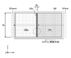
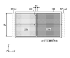
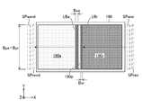
- FIG. 4 is a plan view showing an example of scan irradiation of a line beam on an object to be irradiated.
- FIG. 5 is an enlarged view of a portion surrounded by a broken line circle in FIG.
- the line beam LBa irradiated on the surface of the irradiation object 190 is the line-and-space image pattern of the mask 148 described in FIG. As shown in FIG. 4, the line beam LBa irradiated on the surface of the object to be irradiated 190 has a beam width in the X-axis direction of Bx and a beam width in the Y-axis direction of By.
- the line beam LBa moves relative to the irradiation object 190 by the movement of the XYZ axis stage 172. By moving the XYZ axis stage 172 in the positive direction of the X axis, the line beam LB moves on the surface of the irradiation object 190 in the negative direction of the X axis (leftward in FIG. 4).
- FIG. 4 shows a state of scan irradiation in which the line beam LBa is moved from the scan irradiation initial position SPini to the scan irradiation end position SPaend with respect to the irradiation target 190 to irradiate the surface of the irradiation target 190 with laser light.
- the moving direction of the line beam LBa from the scan irradiation initial position Spaini to the scan irradiation end position Speak is called the "scan irradiation direction" at the time of laser annealing.
- the amorphous silicon is melted and the silicon is polycrystallized by crystal growth 190p. It becomes.
- the crystallization region 190p is a polysilicon film.
- FIG. 5 An enlarged view of the part surrounded by the broken line circle in FIG. 4 is shown in FIG.
- the fluence of the line portion MLI of the imaging pattern of the mask 148 in the line beam LBa irradiated by the irradiation object 190 is lower than that of the space portion MSI. Therefore, in the morphology of the laser-annealed crystal, as shown in FIG. 5, crystal nuclei are generated at positions corresponding to the line portions MLI on the surface of the irradiation object 190, and the space portions MSI between the line portions MLI are generated.
- a large grain boundary 192 is generated at a substantially central portion in the Y-axis direction.
- Scan irradiation is performed while the line beam LBa moves in the negative direction of the X-axis, and when the position of the line beam LBa with respect to the object to be irradiated reaches the scan irradiation end position Spaend (see FIG. 4), the XYZ-axis stage 172 Stop moving.
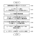
- FIG. 6 is a flowchart showing an example of operation in the laser annealing system 10. The processes and operations shown in the flowchart of FIG. 6 are realized, for example, by a processor functioning as the laser annealing control unit 180 executing a program.
- step S10 the irradiation target 190 is set on the table 174 of the XYZ axis stage 172.
- the irradiation object 190 may be set on the table 174 by a work transfer robot (not shown) or another automatic transfer device.
- step S12 the laser annealing control unit 180 reads (1) the laser irradiation condition parameters during laser annealing.
- the laser irradiation condition parameter at the time of laser annealing is called "laser annealing condition parameter”.
- step S14 the laser annealing control unit 180 causes the laser device 20 to perform adjustment oscillation.
- the laser annealing control unit 180 causes the laser device 20 to oscillate with the repetition frequency f so as to have the target pulse energy Et.
- step S16 the laser annealing control unit 180 controls the XYZ axis stage 172 in the X axis direction and the Y axis direction so that the position of the line beam LB on the irradiation object 190 becomes the initial position.
- step S18 the laser annealing control unit 180 controls the XYZ axis stage 172 in the Z axis direction so that the image of the mask 148 is formed on the surface of the irradiation object 190.
- the laser annealing control unit 180 calculates and sets (1) control parameters for laser annealing. Specifically, the laser annealing controller 180 calculates the transmittance Ta of the attenuator 130 and sets the transmittance Ta so that the fluence Fa is obtained in the case of the line beam width Bx in the short axis direction. In addition, the laser annealing control unit 180 calculates the moving speed Vx of the XYZ axis stage 172 and sets the moving speed Vx so that the irradiation pulse number Na is obtained in the case of the line beam width Bx in the short axis direction.
- step S22 the laser annealing control unit 180 performs beam scan irradiation during laser annealing according to the control parameter settings in step S20.
- pulse laser light is irradiated to the irradiation object 190 under the conditions of the set repetition frequency fa, fluence Fa, and irradiation pulse number Na.
- step S22 the laser annealing control unit 180 ends the flowchart of FIG.
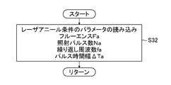
- FIG. 7 is a flowchart showing an example of a subroutine applied to step S12 of FIG. That is, FIG. 7 shows an example of the contents of processing performed in the step (1) of reading parameters of laser irradiation conditions during laser annealing.
- the laser annealing control unit 180 reads the parameters of laser annealing conditions. For example, the laser annealing control unit 180 reads each data of the fluence Fa on the irradiation object 190 when performing the laser annealing process, the irradiation pulse number Na, and the repetition frequency fa.
- the irradiation pulse number Na is an integer of 2 or more.
- the laser annealing control unit 180 returns to the flowchart of FIG. 6 after step S31.
- FIG. 8 is a flowchart showing an example of a subroutine applied to step S14 of FIG. That is, FIG. 8 shows an example of the processing content performed in the step of adjusting oscillation of the laser apparatus.
- the laser annealing control unit 180 transmits the data of the target pulse energy Et and the repetition frequency fa to the laser control unit 38.
- the target pulse energy Et and the repetition frequency fa are data of a rating with which the laser device 20 can operate stably.
- the target pulse energy Et may be a value in the range of 30 mJ to 1000 mJ.
- the repetition frequency fa may be a value in the range of 600 Hz to 6000 Hz.
- the laser annealing control unit 180 may store the rated pulse energy of the laser device 20 as the target pulse energy Et in advance and use this value.
- step S 42 the laser annealing control unit 180 determines whether or not the pulse energy OK signal has been received from the laser control unit 38.
- the determination process in step S42 corresponds to, for example, determining whether or not the difference between the pulse energy E of the pulsed laser light output from the laser device 20 and the target pulse energy Et is within the permissible range.
- the laser annealing control unit 180 repeats step S42 until the determination result of step S42 becomes Yes.
- the laser annealing control unit 180 exits the subroutine of FIG. 8 and returns to the flowchart of FIG.
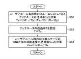
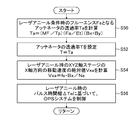
- FIG. 9 is a flowchart showing an example of a subroutine applied to step S20 of FIG. That is, FIG. 9 shows an example of the processing contents performed in the step (1) of calculating and setting the control parameters during laser annealing.
- step S50 of FIG. 9 the laser annealing control unit 180 calculates the transmittance Ta of the attenuator 130 that is the fluence Fa of the laser annealing condition.
- the fluence on the surface of the irradiated object 190 is expressed by the following formula (2).
- M in the equation represents the magnification of the projection optical system 150.
- M may be a value in the range of 1 to 1/5, for example.
- Tp in the formula represents the transmittance of the optical system until the pulsed laser light output from the laser device 20 when the attenuator 130 has the maximum transmittance reaches the irradiation object 190.
- Ta (M 2 /Tp)(Fa/Et)(Bx ⁇ By) (3)
- the laser annealing control unit 180 obtains the transmittance Ta of the attenuator 130 from the equation (3).
- step S52 the laser annealing controller 180 sets the transmittance T of the attenuator 130 to Ta. That is, the laser annealing control unit 180 controls the angles of the partial reflection mirrors 131 and 132 so that the transmittance T of the attenuator 130 becomes Ta.
- step S54 the laser annealing control unit 180 calculates the absolute value Vxa of the moving speed of the XYZ axis stage 172 in the X axis direction during laser annealing.
- Vxa can be calculated from the following equation (4).
- the irradiation pulse number Na during laser annealing is expressed by the following equation (5).
- Na fa ⁇ Bx/Vxa (5)
- Na is the number of pulses (Na ⁇ 2) with which the pulsed laser light is irradiated at the same position.
- the absolute value Vxa of the moving speed can be obtained from the equation (4) obtained by modifying the equation (5).
- step S54 the laser annealing control unit 180 ends the flowchart of FIG. 9 and returns to the flowchart of FIG.
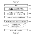
- FIG. 10 is a flowchart showing an example of a subroutine applied to step S22 of FIG. That is, FIG. 10 shows an example of the processing content performed in the step of beam scan irradiation at the time of laser annealing.
- step S62 the laser annealing control unit 180 calculates the moving speed Vx of the XYZ-axis stage 172 in the X-axis direction.
- Vx is determined according to the following equation (6).
- step S64 the laser annealing control unit 180 sets the parameter Vx of the moving speed of the XYZ-axis stage 172 in the X-axis direction according to the calculation result of step S62.
- the parameters are set so that acceleration, constant velocity linear motion, and deceleration are performed at predetermined times according to the moving distance of the beam scan.
- Vxa the absolute value of the velocity during constant-velocity linear motion is Vxa.
- step S66 the laser annealing control unit 180 transmits a movement start signal of the XYZ axis stage 172.
- This movement start signal is a control signal that gives a command to start the movement of the XYZ axis stage 172.
- the XYZ-axis stage 172 starts moving according to the movement start signal transmitted from the laser annealing control unit 180.
- step S68 the laser annealing control unit 180 outputs the light emission trigger signal at the repetition frequency fa.
- step S70 the laser annealing control unit 180 determines whether or not the movement of the XYZ-axis stage 172 in the X-axis direction has been completed. For example, the laser annealing control unit 180 determines whether or not the scan irradiation end position Spaend described with reference to FIG. 4 has been reached. If the determination result of step S70 is No, the laser annealing control unit 180 returns to step S68. Steps S68 to S70 are repeated until the movement of the XYZ-axis stage 172 in the X-axis direction is completed.
- the laser annealing control unit 180 instructs the laser control unit 38 to emit a light emission trigger signal at the repetition frequency fa during the uniform linear motion of the XYZ axis stage 172 in the X axis direction. Is output. As a result, the pulsed laser light is applied to the scan irradiation area of the irradiation object 190 at the repetition frequency fa.
- step S70 When the determination result of step S70 is Yes, that is, when the beam scan irradiation for one scan irradiation region is completed and the movement of the XYZ axis stage 172 in the X axis direction ends, the laser annealing control unit 180 causes the laser annealing controller 180 to perform step S72. And the output of the light emission trigger signal is stopped. As a result, the output of the pulsed laser light from the laser device 20 is stopped.
- step S72 the laser annealing control unit 180 ends the flowchart of FIG. 10 and returns to the flowchart of FIG.
- the imaging pattern of the mask 148 is guided to the irradiated object 190, and the imaging pattern of the mask 148 is scanned and irradiated on the surface of the irradiated object 190.
- the method of performing laser annealing is shown by.
- the irradiation method of the laser light when performing the laser annealing is not limited to this example.
- the XYZ axis stage 172 is fixed, and when the irradiation pulse number Na is reached, the XYZ axis stage 172 is moved to be positioned at the next position and a pulse laser beam is irradiated to the step and repeat method. It may be.
- FIG. 11 is a schematic view of a method of manufacturing a semiconductor crystal thin film by laser annealing.
- an example of the irradiated object 190 in which the amorphous silicon film 202 is arranged on the glass substrate 200 is shown.
- a polysilicon film 204 which is a semiconductor crystal thin film is obtained by melting and polycrystallizing silicon.
- a protrusion (raised portion) of about 50 nm called a ridge 205 is generated on the surface in the process of melting and polycrystallizing silicon.
- a ridge having a height of 50 nm to 70 nm may be generated on the surface of the polysilicon film 204 formed by laser annealing the amorphous silicon film 202 having a film thickness of 50 nm.
- the ridge 205 Since the ridge 205 has a great influence on the characteristics of the semiconductor element formed by using the polysilicon film 204, it is desired to suppress the height of the ridge 205.
- the problem of the ridge 205 is also described in paragraph 0052 of JP-A 2007-287866.
- the threshold voltage of the thin film transistor formed by using the polysilicon film 204 varies due to the influence of the ridge 205, and it may be difficult to lower the power supply voltage.
- a thin film transistor is applied to, for example, a liquid crystal display element, it is difficult to reduce power consumption.
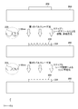
- FIG. 12 is a schematic view exemplifying the method for manufacturing a semiconductor crystal thin film according to the first embodiment.
- the method for producing the semiconductor crystal thin film according to the first embodiment is to irradiate the amorphous silicon film 202 with the first pulsed laser beam to make the amorphous silicon polycrystalline (step 1), and to irradiate the amorphous silicon film 202 with the first pulsed laser beam.
- the ridge 205 of the polycrystalline polysilicon film 204 generated by the above is irradiated with a second pulsed laser beam to flatten the ridge (step 2).
- planearizing the ridge is meant reducing the height of the ridge.
- Step 1 is the process of melting and polycrystallization by laser annealing.
- Step 2 is a step of flattening the polycrystalline ridge produced in Step 1 by laser irradiation.
- laser annealing the operation of step 1
- ridge flattening the operation of step 2
- the irradiation conditions of the laser beam at the time of laser annealing include fluence Fa, pulse time width ⁇ Ta, and irradiation pulse number Na.
- the irradiation conditions of the laser beam at the time of ridge flattening include fluence Fr, pulse time width ⁇ Tr, and irradiation pulse number Nr.
- the pulse time width ⁇ Tr of the second pulse laser light is shorter than the pulse time width ⁇ Ta of the first pulse laser light. That is, ⁇ Tr ⁇ Ta.
- the electric field concentration due to the shape effect of the ridge causes the pulse energy of the laser given to the ridge to be compared with other regions. And grow bigger.
- the crystalline state of the ridge can be improved and the height can be controlled by partially melting the ridge and its periphery without melting and solidifying the entire film.
- the fluence Fr of the second pulse laser light is smaller than the fluence Fa of the first pulse laser light. That is, it is preferable that Fr ⁇ Fa.
- the irradiation pulse number Nr of the second pulse laser light is set to be smaller than the irradiation pulse number Na of the first pulse laser light. That is, it is preferable that Nr ⁇ Na.
- the laser irradiation condition for laser annealing in step 1 is set to a condition for completely melting the amorphous silicon
- the laser irradiation condition for flattening the ridge in step 2 is the ridge of polysilicon generated by polycrystallization of laser annealing.
- the condition is set to lower the part of.
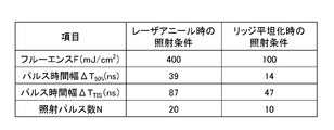
- FIG. 13 is a table showing examples of irradiation conditions applied in the test for producing the semiconductor crystal thin film. It was confirmed that by combining the irradiation conditions shown in FIG. 13, a semiconductor crystal thin film in which the height of the ridge was suppressed to less than 10 nm was obtained.
- the time width is 8%.
- the pulse time width of the full width at half maximum of the pulse laser light for flattening the ridge is preferably 40% or less of the pulse time width of the pulse laser light for laser annealing.
- the TIS pulse time width of the pulsed laser beam for ridge flattening is preferably 60% or less of the pulse time width of the pulsed laser beam for laser annealing.
- (Fa, Na) (50, 20), (100, 10) , (150,10), (200,1) and so on.
- the unit of fluence Fa is millijoule per square centimeter [mJ/cm 2 ] as in FIG. 13.
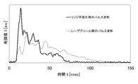
- FIG. 14 is a graph showing an example of the pulse waveform of the laser light used in the test.
- the pulse waveform at the time of ridge flattening has a shorter pulse time width than the pulse waveform at the time of laser annealing.
- the heads of both pulses are aligned and displayed in order to compare the pulse time widths.
- the same position (irradiation region) of the object to be irradiated 190 is irradiated with the second pulse laser light after the irradiation of the first pulse laser light. Therefore, there is a time difference between the two pulses as the timing of irradiation of the first pulse laser light and the second pulse laser light with respect to the same position of the object to be irradiated 190.
- irradiation of the second pulse laser beam to the same region is started after the silicon film is polycrystallized by the irradiation of the first pulse laser beam, that is, after the ridge 205 is formed.
- the melting and polycrystallization times by the irradiation with the first pulsed laser light are approximately 200 ns. Therefore, for example, after 200 ns or more (that is, after crystallization) from the irradiation timing of the first pulse laser light that is the laser annealing pulse, the second pulse laser light that is the ridge flattening pulse is used as the first pulse laser light. It suffices to irradiate the same area (place) as the light irradiation area. As a result, the ridge 205 formed by polycrystallization can be partially melted and the ridge 205 can be flattened.
- FIG. 15 shows a configuration example of an optical pulse stretcher (OPS) system for adjusting the pulse time width.
- OPS optical pulse stretcher
- the OPS system 220 shown in FIG. 15 includes a first OPS 221 and a second OPS 222.
- Each of the first OPS 221 and the second OPS 222 may have the same configuration as the OPS system 32 described with reference to FIG.
- the first OPS 221 includes a beam splitter 230 and concave mirrors 231 to 234.
- the second OPS 222 includes a beam splitter 240 and concave mirrors 241 to 244.
- the second OPS 222 is arranged so that the laser light transmitted through the beam splitter 230 of the first OPS 221 is incident on the beam splitter 240 of the second OPS 222.
- the OPS system 220 is arranged on the optical path between the excimer laser device 210 and the laser annealing device 100.
- the excimer laser device 210 may be, for example, the master oscillator 30 described with reference to FIG.
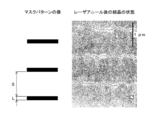
- FIG. 16 shows an example of a mask pattern and crystal growth.
- FIG. 16 shows an example of an image of a mask pattern and a state of crystals after laser annealing.
- the left figure of FIG. 16 shows an image of a mask pattern projected on the surface of the irradiated object 190.
- the right figure of FIG. 16 shows the state of the crystal after laser annealing at the position corresponding to the image of the mask pattern.
- the right diagram of FIG. 16 shows a sample obtained by etching the ridge portion to remove the ridge portion (crystal grain boundary) by observing it with a scanning electron microscope (SEM). It is an example of the image of.
- the lines that look like “cracks” are the grain boundaries.
- a thick grain boundary is generated at a substantially intermediate position in the space portion of the mask pattern image.
- irradiating the pulse for laser annealing for example, 200 ns or more, irradiate the pulse for flattening the ridge.
- the ridge is partially melted and flattened.
- “Flatness” implies that the ridge is suppressed to an acceptable height (eg, less than 10 nm), that is, the flatness is improved.
- FIG. 17 schematically shows the configuration of the laser annealing system 11 according to the first embodiment. Differences between the configuration shown in FIG. 17 and FIG. 2 will be described.
- the laser annealing system 11 shown in FIG. 17 differs from the configuration of FIG. 2 in that the beam splitter 70 of the OPS system 32 includes an optical element switching unit 82 that can replace the window 80.
- the laser annealing control unit 180 arranges the beam splitter 70 on the optical path at the time of laser annealing and arranges the window 80 on the optical path instead of the beam splitter 70 at the time of flattening the ridge.
- the optical element switching unit 82 is controlled.
- FIG. 18 is a plan view showing an example of beam scan irradiation at the time of ridge flattening in the first embodiment.
- the line beam LBr irradiated on the surface of the irradiation object 190 during the ridge flattening includes an image of the line and space pattern of the mask 148 described in FIG.
- the line beam LBr with which the surface of the irradiation object 190 is irradiated has a beam width in the X-axis direction of Bx and a beam width in the Y-axis direction of By.
- the line beam LBr moves relative to the irradiated object 190 due to the movement of the XYZ axis stage 172.
- the line beam LBr moves on the surface of the irradiation object 190 in the positive direction of the X axis (rightward in FIG. 18).
- FIG. 18 shows a state of scan irradiation in which the surface of the irradiation object 190 is irradiated with laser light by moving the line beam LBr from the scanning irradiation initial position SPrini to the irradiation object 190 to the scanning irradiation end position SPrend.
- the moving direction of the line beam LBr from the scan irradiation initial position SPrini toward the scan irradiation end position SPrend is referred to as a "scan irradiation direction during ridge flattening".
- the scan irradiation initial position SPrini at the time of ridge flattening may be the scan irradiation end position SPrind at the time of laser annealing described in FIG.
- the scan irradiation end position SPrend during the ridge flattening shown in FIG. 18 may be the scan irradiation initial position SPaini during laser annealing described in FIG.
- a region of the surface of the irradiation object 190 through which the line beam LBr passes that is, a region where scan irradiation for ridge flattening is performed becomes a ridge flattening region 190r in which the ridge is flattened.
- the region through which the line beam LBr does not pass, that is, the region where the scan irradiation for ridge flattening is not performed is the crystallization region 190p in which the high ridge is still contained.
- the entire crystallization region 190p can be changed to the ridge flattening region 190r.
- FIG. 19 is a flowchart showing an example of operation in the laser annealing system 11 according to the first embodiment. The difference between FIG. 19 and FIG. 6 will be described.
- the flowchart shown in FIG. 19 includes steps S13 and S21 in place of steps S12 and S20 of FIG. 6, and steps S24, S26, and S28 are added after step S22.
- step S13 the laser annealing control unit 180 reads the laser irradiation condition parameter at the time of laser annealing (2). Steps S14 to S18 after step S13 are the same as in FIG.
- step S21 the laser annealing control unit 180 calculates and sets (2) control parameters for laser annealing.
- Step S22 after step S21 is the same as in FIG.
- step S24 the laser annealing control unit 180 reads (1) the laser irradiation condition parameters for flattening the ridge.
- step S26 the laser annealing control unit 180 calculates and sets (1) control parameters for flattening the ridge.
- step S28 the laser annealing control unit 180 performs beam scan irradiation at the time of ridge flattening according to the setting of the control parameters in step S26.
- the irradiation object 190 is irradiated with the pulsed laser light under the conditions of the set repetition frequency fr, fluence Fr, and irradiation pulse number Nr.
- step S28 the laser annealing control unit 180 ends the flowchart of FIG.
- FIG. 20 is a flowchart showing an example of a subroutine applied to step S13 of FIG. That is, FIG. 20 shows an example of the processing content carried out in the step (2) of reading the laser irradiation condition parameter at the time of laser annealing.
- the laser annealing control unit 180 reads the parameters of the laser annealing conditions. For example, the laser annealing control unit 180 reads each data of the fluence Fa on the irradiation object 190 when performing the laser annealing process, the irradiation pulse number Na, the repetition frequency fa, and the pulse time width ⁇ Ta.
- the irradiation pulse number Na is an integer of 2 or more.
- the laser annealing control unit 180 returns to the flowchart of FIG. 19 after step S32.
- FIG. 21 is a flowchart showing an example of a subroutine applied to step S21 of FIG. That is, FIG. 21 shows an example of processing contents performed in the step (2) of calculation and setting of control parameters during laser annealing. The differences between FIG. 21 and FIG. 9 will be described.
- step S56 is added to steps S50 to S54 of FIG.
- the laser annealing control unit 180 controls the OPS system 32 based on the pulse time width ⁇ Ta at the time of laser annealing.
- the laser annealing control unit 180 controls the OPS system 32 so that the pulse time width of the pulsed laser light emitted from the OPS system 32 is close to the pulse time width ⁇ Ta required as a condition for laser annealing.
- the laser annealing control unit 180 controls the optical element switching unit 82 so as to arrange the beam splitter 70 on the optical path.
- step S56 the laser annealing control unit 180 ends the flowchart of FIG. 21 and returns to the flowchart of FIG.
- FIG. 22 is a flowchart showing an example of a subroutine applied to step S24 of FIG. That is, FIG. 22 shows an example of the processing content performed in the step (1) of reading the laser irradiation condition parameter at the time of ridge flattening.
- the laser irradiation condition parameters for flattening the ridge are referred to as “parameters for flattening the ridge”.
- the laser annealing control unit 180 reads the parameters of the ridge flattening condition. For example, the laser annealing control unit 180 reads each data of the fluence Fr on the irradiated object 190 when performing the ridge flattening process, the number of irradiation pulses Nr, the repetition frequency fr, and the pulse time width ⁇ Tr. ..
- the irradiation pulse number Nr is an integer of 1 or more.
- the laser annealing controller 180 returns to the flowchart of FIG. 19 after step S80.
- FIG. 23 is a flowchart showing an example of a subroutine applied to step S26 of FIG. That is, FIG. 23 shows an example of the processing content executed in the step of calculation and setting (1) of the control parameter at the time of ridge flattening.
- the laser annealing control unit 180 calculates the transmittance Tr of the attenuator 130, which is the fluence Fr under the ridge flattening condition.
- the transmittance Tr of the attenuator 130 can be obtained from the equation (2) to the following equation (7).
- Tr (M 2 /Tp)(Fr/Et)(Bx ⁇ By) (7)
- the laser annealing controller 180 sets the transmittance T of the attenuator 130 to Tr. That is, the laser annealing controller 180 controls the angles of the partial reflection mirrors 131 and 132 so that the transmittance T of the attenuator 130 becomes Tr.
- step S94 the laser annealing control unit 180 calculates the absolute value Vxr of the speed at which the line beam LBr moves on the surface of the irradiation object 190 during flattening of the ridge. That is, the laser annealing control unit 180 calculates the absolute value Vxr of the moving speed of the XYZ-axis stage 172 in the X-axis direction at the time of ridge flattening. Vxr can be calculated from the following equation (8).
- the laser annealing control unit 180 controls the OPS system 32 based on the pulse time width ⁇ Tr for flattening the ridge.
- the laser annealing control unit 180 controls the OPS system 32 so that the pulse time width of the pulsed laser light emitted from the OPS system 32 is close to the pulse time width ⁇ Tr required as a condition for flattening the ridge.
- the laser annealing control unit 180 controls the optical element switching unit 82 so that the window 80 is arranged on the optical path.
- step S96 the laser annealing control unit 180 ends the flowchart of FIG. 23 and returns to the flowchart of FIG.
- FIG. 24 is a flowchart showing an example of a subroutine applied to step S28 of FIG. That is, FIG. 24 shows an example of the processing content performed by the beam scan irradiation at the time of ridge flattening.
- step S102 the laser annealing control unit 180 calculates the moving speed Vx of the XYZ-axis stage 172 in the X-axis direction.
- Vx is determined according to the following equation (9).
- step S104 the laser annealing control unit 180 sets the parameter Vx of the moving speed of the XYZ-axis stage 172 in the X-axis direction according to the calculation result of step S102.
- the parameters are set so that acceleration, constant velocity linear motion, and deceleration are performed at predetermined times according to the moving distance of the beam scan.
- Vxr the absolute value of the velocity during constant-velocity linear motion is illustrated.
- step S106 the laser annealing control unit 180 transmits a movement start signal for the XYZ axis stage 172.
- Vx determined from the equation (9) is negative
- the XYZ-axis stage 172 is moved in the negative direction of the X-axis.
- the line beam LBr moves in the positive direction of the X-axis relative to the irradiated object 190.
- step S108 of FIG. 24 the laser annealing control unit 180 outputs a light emission trigger signal at the repetition frequency fr.
- step S110 the laser annealing control unit 180 determines whether or not the movement of the XYZ-axis stage 172 in the X-axis direction has been completed.
- the laser annealing control unit 180 determines whether or not the scanning irradiation end position SPrend shown in FIG. 18 has been reached. If the determination result in step S110 is No, the laser annealing control unit 180 returns to step S108. Steps S108 to S110 are repeated until the movement of the XYZ axis stage 172 in the X axis direction is completed.
- the laser annealing controller 180 outputs a light emission trigger signal to the laser controller 38 at the repetition frequency fr during the uniform linear motion of the XYZ axis stage 172 in the X-axis direction.
- the pulsed laser beam is applied to the scan irradiation region of the object to be irradiated 190 at the repetition frequency fr.
- step S110 determines whether the beam scan irradiation for one scan irradiation region is completed and the movement of the XYZ axis stage 172 in the X axis direction is completed.
- the laser annealing control unit 180 is set to step S112. To stop the output of the light emission trigger signal. As a result, the output of the pulsed laser light from the laser device 20 is stopped.
- step S112 the laser annealing control unit 180 ends the flowchart of FIG. 24 and returns to the flowchart of FIG.
- one laser device can output two types of pulse laser lights having different pulse time widths. Laser annealing and ridge flattening can be performed using these two types of pulsed laser beams.
- the laser device 20 in the first embodiment is an example of the "laser system” in the present disclosure.
- the master oscillator 30 is an example of the “laser oscillator” in the present disclosure.
- the XYZ axis stage 172 is an example of the "moving mechanism” in the present disclosure.
- the laser annealing control unit 180 is an example of the “control unit” in the present disclosure.
- the optical system including the illumination optical system 140 and the projection optical system 150 of the irradiation optical system 110 is an example of the “irradiation optical system” in the present disclosure.
- Each of the beam splitter 70 and the window 80 of the optical element switching unit 82 is an example of the “optical element” in the present disclosure.
- the projection optical system 150 is an example of the “transfer optical system” in the present disclosure.
- the amorphous silicon film 202 is an example of the “amorphous semiconductor” in the present disclosure.
- the region irradiated with the line beam LBa for laser annealing and polycrystallized is an example of the “semiconductor crystal region” in the present disclosure.
- the polysilicon film 204 is an example of the "semiconductor crystal" and the "semiconductor crystal thin film” in the present disclosure.
- the line beam LBa irradiated to the irradiated object 190 is an example of the “first pulsed laser light illumination pattern” in the present disclosure
- the line beam LBr irradiated to the irradiated object 190 is the “second pulse laser light illumination pattern” in the present disclosure. It is an example of the "illumination pattern of a pulsed laser beam.”
- the pulse time width ⁇ Ta of the pulsed laser beam for laser annealing is an example of the “first pulse time width” in the present disclosure.
- the pulse time width ⁇ Tr of the pulsed laser beam for ridge flattening is an example of the “second pulse time width” in the present disclosure.
- the OPS system may include a plurality of optical pulse stretchers. Good.
- an optical element switching unit similar to the optical element switching unit 82 may be arranged in each of the plurality of optical pulse stretchers arranged in the OPS system to control the switching of optical elements.
- the OPS system 32 may be arranged in the optical path between the laser annealing apparatus 100 and the laser apparatus 20.
- a method of performing laser annealing and ridge flattening by performing beam scan irradiation in which the imaging pattern of the mask 148 is moved on the object to be irradiated 190 is shown, but the present invention is not limited to this example. ..
- laser irradiation may be performed by the step and repeat method under the irradiation conditions at the time of laser annealing, and then laser irradiation may be performed by the step and repeat method under the irradiation conditions at the time of ridge flattening at the time of ridge flattening.
- FIG. 25 schematically shows the configuration of the laser annealing system 12 according to the second embodiment. Differences between the configuration shown in FIG. 25 and FIG. 17 will be described.
- the laser annealing system 12 shown in FIG. 25 differs from the configuration of FIG. 17 in that a shutter 84 for opening and closing the delay optical path is arranged on the delay optical path of the OPS 33 instead of the optical element switching unit 82 of FIG. ..
- Other configurations are the same as in FIG.
- the laser annealing controller 180 controls the opening/closing operation of the shutter 84 via the laser controller 38.
- the reflectance of the beam splitter 70 of the OPS 33 is preferably 55% to 65%, more preferably 60%.
- the laser annealing controller 180 outputs a delayed optical path opening/closing control signal for operating the shutter 84.
- the delayed optical path opening/closing control signal transmitted from the laser annealing control unit 180 is transmitted to the drive unit of the shutter 84 via the laser control unit 38.
- a control signal for opening the shutter 84 is transmitted from the laser annealing control unit 180.
- the pulse laser light pulse-stretched by the OPS 33 is applied to the irradiation object 190.
- the pulsed laser light pulse-stretched by the OPS 33 is an example of the “first pulsed laser light” in the present disclosure.
- a control signal for closing the shutter 84 is transmitted from the laser annealing control unit 180.
- the shutter 84 is closed, the delayed optical path of the OPS 33 is blocked, so that the pulse laser light that has not been pulse stretched by the OPS 33 is applied to the irradiation target 190.
- the pulse laser light that is not pulse stretched by the OPS 33 that is, the pulse laser light that has passed through the beam splitter 70 when the shutter 84 is in the closed state is an example of the “second pulse laser light” in the present disclosure.
- the pulse laser light for laser annealing and the pulse laser light for flattening the ridge are switched and irradiated only by controlling the opening/closing operation of the shutter 84. can do.
- FIG. 26 schematically shows the configuration of the laser annealing system 13 according to the third embodiment. Differences between the configuration shown in FIG. 26 and FIG. 17 will be described.
- the laser annealing system 13 according to the third embodiment has a first laser device 21 that outputs a first pulsed laser beam for laser annealing and a second laser that outputs a second pulsed laser beam for ridge flattening.
- a device 22, a first lightpath tube 26, and a second lightpath tube 27 are included.
- the first laser device 21 and the first optical path tube 26 may have the same configuration as the laser device 20 and the optical path tube 25 described with reference to FIG.
- the first optical path tube 26 is arranged on the optical path of the laser beam between the laser beam emitting port of the first laser device 21 and the first laser beam incident port of the laser annealing device 100.
- the second laser device 22 outputs a second pulse laser light having a pulse time width shorter than the pulse time width of the first pulse laser light output from the first laser device 21.
- the second laser device 22 may be a laser device having a configuration in which the OPS system 32 is deleted from the configuration of the first laser device 21.
- the second optical path tube 27 is arranged on the optical path of the laser beam between the laser beam emitting port of the second laser device 22 and the second laser beam incident port of the laser annealing device 100.
- the irradiation optical system 113 of the laser annealing system 13 has, in addition to the configuration of the irradiation optical system 110 described with reference to FIG. 17, a high reflection for irradiating the irradiation target 190 with the second pulsed laser light for flattening the ridge.
- Mirrors 321 to 323, an attenuator 330, and an illumination optical system 340 are added.
- the high-reflection mirror 321 is arranged so that the laser light that has passed through the second optical path tube 27 passes through the attenuator 330 and is incident on the high-reflection mirror 322.
- the attenuator 330 is arranged on the optical path between the high reflection mirror 321 and the high reflection mirror 322.
- the attenuator 330 includes two partial reflection mirrors 331 and 332, and rotating stages 335 and 336 that change the incident angle of the partial reflection mirrors 331 and 332, respectively.
- the high-reflection mirror 322 is arranged so that the laser light passing through the attenuator 330 enters the high-reflection mirror 323.
- the high-reflection mirror 323 is arranged so that the incident pulsed laser light is incident on the fly-eye lens 345 of the illumination optical system 340.
- the illumination optical system 340 includes a fly-eye lens 345 and a condenser lens 346.
- the illumination optical system 340 is an optical system for uniformly illuminating a predetermined illumination area on the mask 148, and is arranged so as to perform Koehler illumination on the mask 148 with a rectangular beam.
- the fly-eye lens 345 is arranged so that, for example, the focal plane of the fly-eye lens 345 and the front focal plane of the condenser lens 346 coincide with each other, and the condenser lens 346 is positioned between the rear focal plane of the condenser lens 346 and the mask 148. Are arranged so that and match.
- the line beam LBa for laser annealing that irradiates the surface of the irradiated object 190 via the illumination optical system 140 and the projection optical system 150 has a beam width in the Y-axis direction of Bya on the surface of the irradiated object 190.
- the beam width in the X-axis direction is Bxa.
- the line beam LBr for flattening the ridge that is irradiated onto the surface of the irradiation target 190 via the illumination optical system 340 and the projection optical system 150 has a beam width in the Y-axis direction on the surface of the irradiation target 190. It is assumed that it is Byr and the beam width in the X-axis direction is Bxr.
- the number of irradiation pulses at the time of laser annealing is Na
- the number of irradiation pulses at the time of ridge flattening is Nr.
- 340 is configured.
- the fly-eye lens 145 of the illumination optical system 140 and the fly-eye lens 345 of the illumination optical system 340 have the same pitch interval in the Y-axis direction, and the ratio of the pitch intervals in the X-axis direction is the same as the ratio of Na to Nr.
- the focal lengths of the condenser lenses 146 and 346 of the illumination optical system 140 and the illumination optical system 340 may be the same.
- the operation of performing laser annealing by irradiating the irradiated object 190 with the pulsed laser light output from the first laser device 21 is the same as that of the laser annealing system 10 described with reference to FIG.
- the laser annealing control unit 180 transmits/receives various data such as target pulse energy and signals to/from a laser control unit (not shown) of the second laser device 22.
- the laser annealing control unit 180 transmits the light emission trigger signal Tr2 to the second laser device 22 in synchronization with the light emission trigger Tr1 of the first laser device 21.
- the pulsed laser light output from the second laser device 22 passes through the second optical path tube 27, is reflected by the high reflection mirror 321, and enters the attenuator 330.
- the pulsed laser light transmitted through the attenuator 330 is incident on the illumination optical system 340 via the high reflection mirrors 322 and 323.
- the pulsed laser light that has passed through the illumination optical system 340 is shaped into a line beam having a rectangular beam shape and a uniform light intensity, and is irradiated onto the mask 148.
- FIG. 27 is a plan view showing an example of the relationship between the pattern of the mask 148 and the line beams LBam and LBrm that illuminate the mask 148. As shown in FIG. 27, the line beam LBam for laser annealing and the line beam LBrm for ridge flattening are irradiated on the mask 148, respectively.
- the laser annealing control unit 180 controls the transmittance of the attenuator 130 so that the fluence of the laser annealing line beam LBa on the surface of the irradiation object 190 becomes Fa. Further, the laser annealing control unit 180 controls the transmittance of the attenuator 330 so that the fluence of the ridge flattening line beam LBr on the surface of the irradiation object 190 becomes Fr.
- the moving speed Vxa of the XYZ axis stage 172 in the X axis direction at the time of laser annealing is obtained by the following equation (10).
- Vxa fa ⁇ Bxa/Na (10)
- the moving speed Vxr of the XYZ axis stage 172 in the X axis direction when the ridge is flattened is expressed by the following equation (11).
- Vxr fr ⁇ Bxr/Nr (11)
- fa fr
- Vxa Vxr.
- FIG. 28 is a plan view showing an example of scan irradiation of a line beam on the irradiated object 190.
- Laser irradiation and ridge flattening are performed by scanning and irradiating the irradiation object 190 with two line beams, that is, a line beam LBa for laser annealing and a line beam LBr for flattening the ridge. can do.
- the line beam LBa for laser annealing applied to the surface of the irradiation object 190 is the line-and-space image forming pattern of the mask 148 described with reference to FIG. As shown in FIG. 28, the line beam LBa for laser annealing irradiated on the surface of the object to be irradiated 190 has a beam width in the X-axis direction of Bxa and a beam width in the Y-axis direction of Bya.
- the line beam LBr for ridge flattening irradiated on the surface of the object to be irradiated 190 has a beam width in the X-axis direction of Bxr and a beam width in the Y-axis direction of Byr.
- Bya Byr.
- the two line beams LBa and LBr move relative to the irradiated object 190 due to the movement of the XYZ axis stage 172.
- the line beams LBa and LBr move the surface of the object to be irradiated 190 in the negative direction of the X-axis (leftward in FIG. 28).
- the line beam LBa for laser annealing moves from the scan irradiation initial position SPani to the scan irradiation end position Buck with respect to the irradiated object 190.
- the line beam LBr for ridge flattening follows the movement of the line beam LBa for laser annealing and moves from the scan irradiation initial position SPrini to the scan irradiation end position SPrend with respect to the irradiated object 190.
- a region of the surface of the irradiation object 190 where the line beam LBa does not pass that is, a region where scan irradiation is not performed, is not yet irradiated with laser light and is amorphous (amorphous).
- the amorphous region 190a remains in this state.
- the region of the surface of the irradiated object 190 through which the line beam LBa has passed is a crystallization region 190p in which silicon is polycrystalline due to crystal growth.
- the region of the surface of the irradiated object 190 through which the line beam LBr for ridge flattening has passed is the ridge flattening region 190r in which the ridge is flattened.
- a region of the surface of the object to be irradiated 190 which is a region through which the laser annealing line beam LBa has passed and which does not pass through the ridge flattening line beam LBr, is a crystal containing a ridge. This is a converted region 190p.
- the laser annealing system 13 according to the third embodiment has the following actions and effects as compared with the laser annealing system 11 according to the first embodiment.
- the amount of dimming can be reduced. This improves the utilization efficiency of the pulsed laser light.
- Laser annealing and ridge flattening can be performed by one scan irradiation operation in the X-axis direction of the XYZ-axis stage 172, and throughput is improved.
- the combination of the first laser device 21 and the second laser device 22 in the third embodiment is an example of the “laser system” in the present disclosure.
- FIG. 29 schematically shows the configuration of the laser annealing system 14 according to the fourth embodiment. Differences between the configuration shown in FIG. 29 and FIG. 26 will be described.
- the laser annealing system 14 shown in FIG. 29 includes a laser device 23 and a branching system 250 in place of the first laser device 21 and the second laser device 22 in FIG. 26.
- the laser device 23 is an excimer laser device that does not include an OPS system.
- the laser device 23 may have, for example, a configuration in which the OPS system 32 is deleted from the laser device 20 described in FIG. 2, and includes the master oscillator 30, the monitor module 34, and the laser control unit 38.
- a third optical path tube 28, a branching system 250, a first optical path tube 26 and a second optical path tube 27 are arranged on the optical path between the laser device 23 and the laser annealing device 100.
- the third optical path tube 28 is arranged on the optical path of the laser light between the laser light emitting port of the laser device 23 and the laser light incident port of the branching system 250.
- the branching system 250 includes a beam splitter 254, an OPS system 32, and a high reflection mirror 257.
- the beam splitter 254 is arranged on the optical path of laser light between the laser device 23 and the OPS system 32.
- the beam splitter 254 is coated with a partially reflective film.
- the reflected light reflected by the beam splitter 245 is arranged so as to enter the high reflection mirror 321 of the laser annealing apparatus 100 via the high reflection mirror 257 and the second optical path tube 27.
- the reflectance R4 of the beam splitter 254 is a value close to the reflectance calculated by the following formula (12).
- the OPS system 32 is on the optical path of the transmitted light of the beam splitter 254 and is arranged between the high reflection mirror 121 of the laser annealing device 100 and the beam splitter 254.
- the laser annealing control unit 180 transmits the light emission trigger signal Tr3 to the laser device 23.
- the pulsed laser light output from the laser device 23 enters the branching system 250.
- the pulsed laser light reflected by the beam splitter 254 is not pulse-stretched, passes through the high-reflection mirror 257 and the second optical path tube 27, and enters the high-reflection mirror 321.
- the pulsed laser light highly reflected by the high-reflection mirror 321 is incident on the attenuator 330.
- the pulsed laser light transmitted through the attenuator 330 enters the illumination optical system 340 via the high reflection mirrors 322 and 323.
- the pulsed laser light transmitted through the illumination optical system 340 has a rectangular beam shape, is shaped into a line beam whose light intensity is spatially uniform, and irradiates the mask 148 as a line beam LBrm for ridge flattening. To be done.
- the relationship between the line beam LBrm and the pattern of the mask 148 is the same as in FIG. 27.
- the pulsed laser light transmitted through the beam splitter 254 of the branching system 250 is pulse-stretched by the OPS system 32 and incident on the illumination optical system 140 via the high-reflection mirror 121, the attenuator 130, the high-reflection mirror 122 and 123. ..
- the pulsed laser light transmitted through the illumination optical system 140 has a rectangular beam shape, is shaped into a line beam having a spatially uniform light intensity, and is irradiated onto the mask 148 as a line beam LBam for laser annealing. It The relationship between the line beam LBam and the pattern of the mask 148 is the same as in FIG. 27.
- the scanning irradiation operation for laser annealing and ridge flattening for the irradiation target 190 is the same as the scanning irradiation operation of the third embodiment described in FIG. 28.
- the laser annealing system 14 according to the fourth embodiment can perform laser annealing and ridge flattening with one laser device 23 as compared with the configuration of the third embodiment shown in FIG.
- the reflectance R4 of the beam splitter 254 is closer to the value of the equation (12) as compared with the first embodiment (17) and the second embodiment (25). By doing so, the utilization efficiency of the pulsed laser beam is improved.
- the laser device 23 in the fourth embodiment is an example of the "third laser device” in the present disclosure.
- the combination of the laser device 23 and the branching system 250 is an example of the "laser system” in the present disclosure.
- the branching system 250 is arranged between the laser annealing device 100 and the laser device 23, but the branching system 250 is not limited to this example. May be arranged in the laser apparatus 23 or in the laser annealing apparatus 100.
- the attenuator 330 does not have to be arranged as long as it is within the control range of the pulse energy of the pulse laser light of the laser device 23.
- FIG. 30 schematically shows the configuration of the laser annealing system 15 according to the fifth embodiment. Differences between the configuration shown in FIG. 30 and FIG. 29 will be described.
- the laser annealing system 15 shown in FIG. 30 includes a laser device 24 and a polarization branching system 251 instead of the laser device 23 and the branching system 250 in FIG.
- the laser device 24 is an excimer laser device that does not include an OPS system, and is a laser device that outputs a linearly polarized pulsed laser light that is orthogonal to the XZ plane.
- Two windows (not shown) in the optical resonator of the laser device 24 may be arranged at a brewer angle so that the polarized light orthogonal to the XZ plane becomes P-polarized light.
- the polarization branching system 251 is arranged on the optical path between the laser device 24 and the laser annealing device 100.
- the second optical path tube 27 shown in FIG. 29 is deleted.
- the polarization branching system 251 includes a retarder 255 and an OPS system 32.
- the retarder 255 is arranged on the optical path between the OPS system 32 and the laser device 24.
- the retarder 255 is a ⁇ /2 plate, and the material of the retarder 255 is, for example, crystal, MgF 2 crystal, or sapphire crystal.
- the retarder 255 further includes a rotary stage 256 that rotates an angle ⁇ formed by the optical axis of the retarder 255 and the polarization plane of the pulsed laser light incident on the retarder 255.
- the OPS system 32 is arranged on the optical path of laser light between the laser device 24 and the laser annealing device 100.
- the beam splitter 70P arranged in the OPS system 32 is coated with a film that partially reflects the S-polarized component and highly transmits the P-polarized component, and is arranged so that the polarized component orthogonal to the XZ plane becomes the S-polarized component.
- the high reflection mirrors 121 and 321 of FIG. 29 have been deleted, and instead, a polarization beam splitter 324 and a high reflection mirror 325 have been added.
- the polarization beam splitter 324 is arranged so that the pulsed laser light having a polarization plane orthogonal to the XZ plane becomes S-polarized light and enters the attenuator 130.
- the polarization beam splitter 324 is coated with a film that highly reflects S-polarized light and highly transmits P-polarized light.
- the high reflection mirror 325 reflects the transmitted light of the polarizing beam splitter 324, and is arranged so that the reflected light is incident on the attenuator 330.
- the laser device 24 outputs pulsed laser light having a plane of polarization orthogonal to the XZ plane.
- the pulsed laser light output from the laser device 24 enters the retarder 255.
- the retarder 255 rotates the plane of polarization of the pulsed laser light by 2 ⁇ .
- the pulsed laser light whose plane of polarization is rotated is incident on the beam splitter 70p.
- a part of the pulsed laser light having a polarization component orthogonal to the XZ plane is reflected by the beam splitter 70p of the OPS system 32, and the other part is transmitted through the beam splitter 70p, and thus pulse-stretched by the OPS system 32. ..
- the pulsed laser light of the polarization component including the XZ plane is highly transmitted through the beam splitter 70p and is not pulse stretched.
- the pulsed laser light that has passed through the OPS system 32 enters the polarization beam splitter 324 of the irradiation optical system 114.
- the polarization component orthogonal to the XZ plane pulse-stretched by the OPS system 32 is highly reflected by the polarization beam splitter 324, and enters the illumination optical system 140 via the attenuator 130 and the high-reflection mirrors 122 and 123.
- the pulsed laser light that has passed through the illumination optical system 140 is shaped into a rectangular line beam having a uniform intensity distribution, and is irradiated onto the mask 148 for laser annealing.
- the polarization component including the XZ plane not pulse-stretched by the OPS system 32 is highly transmitted by the polarization beam splitter 324, and is transmitted to the illumination optical system 340 via the high reflection mirror 325, the attenuator 330, and the high reflection mirrors 322 and 323. Incident.
- the pulsed laser light that has passed through the illumination optical system 340 is shaped into a rectangular line beam having a uniform intensity distribution, and is irradiated onto the mask 148 for flattening the ridge.
- the operation of irradiating the irradiated object 190 with the pulsed laser light for laser annealing and the pulsed laser light for ridge flattening that have passed through the mask 148 via the projection optical system 150 is the same as that of the fourth embodiment.
- the laser annealing control unit 180 has a ratio Rab of the pulse energy Ea of the pulsed laser light of the polarized component orthogonal to the XZ plane of the pulsed laser light transmitted through the retarder 255 and the pulse energy Eb of the pulsed laser light of the polarized component including the XZ plane.
- the retarder 255 is rotated so as to satisfy the relationship of the following expression (13).
- the ratio of the pulsed laser light for laser annealing and the pulsed laser light for ridge flattening is adjusted by rotating the optical axis of the retarder 255 as compared with the third embodiment shown in FIG. By doing so, the utilization efficiency of the pulsed laser beam is improved.
- the utilization efficiency of the pulsed laser light is adjusted by adjusting the ratio of the pulsed laser light for laser annealing and the pulsed laser light for ridge flattening. Can be optimized.
- the combination of the laser device 24 and the polarization splitting system 251 according to the fifth embodiment is an example of the “laser system” in the present disclosure.
- the laser device 24 is an example of the “fourth laser device” in the present disclosure.
- the polarization component orthogonal to the XZ plane is an example of the "first polarization component” in the present disclosure.
- the polarization component including the XZ plane is an example of the "second polarization component" in the present disclosure.
- the polarization splitting system 251 is arranged between the laser annealing device 100 and the laser device 24.
- the present invention is not limited to this example. It may be arranged in the apparatus 24 or in the laser annealing apparatus 100.
- the attenuator 330 does not have to be arranged as long as it is within the control range of the pulse energy of the pulsed laser beam of the laser device 24.
- FIG. 31 schematically shows the configuration of the laser annealing system 16 according to the sixth embodiment.
- the projection optical system 151 is used to locally laser-anneal the region portion of the irradiated object 190 that forms the TFT. Differences between the configuration shown in FIG. 31 and FIG. 26 will be described.
- the irradiation optical system 115 of the laser annealing system 16 shown in FIG. 31 includes illumination optical systems 141 and 341 in place of the illumination optical systems 140 and 340 of FIG. 26. Further, the laser annealing system 16 includes a mask 149 and a projection optical system 151 instead of the mask 148 and the projection optical system 150 in FIG. 26.
- the first pulsed laser light for laser annealing output from the first laser device 21 enters the illumination optical system 141 via the high reflection mirror 121, the attenuator 130, and the high reflection mirrors 122 and 123.
- the second pulsed laser beam for ridge flattening output from the second laser device 22 is incident on the illumination optical system 341 via the high reflection mirror 321 and the attenuator 330, and the high reflection mirrors 322 and 323.
- Each of the illumination optical systems 141 and 341 is an optical system for uniformly illuminating a predetermined illumination area on the mask 148, and is arranged so that the mask 149 is Koehler-illuminated with a rectangular beam.
- FIG. 32 shows an example of the irradiation region of the beam on the mask 149 and the mask 149.
- the mask 149 includes a plurality of pattern regions 149pa for forming a plurality of TFTs and a shielding region 149sh. The same fine pattern that promotes crystal growth is formed in each of the plurality of pattern regions 149pa (see FIG. 33).
- FIG. 32 shows a uniform illumination region LB1 m by the illumination optical system 141 and a uniform illumination region LB2 m by the illumination optical system 341.
- the uniform illumination region LB1m is an illumination region of a uniform beam for laser annealing.
- the uniform illumination region LB2m is an irradiation region of a uniform beam for ridge flattening.
- the number of pattern areas 149pa in the X-axis direction within the uniform illumination area LB1m by the illumination optical system 141 is a number corresponding to the irradiation pulse number Na during laser annealing.
- the number of pattern regions 149pa in the X-axis direction in the uniform illumination region LB2m by the illumination optical system 341 is the number corresponding to the irradiation pulse number Nr at the ridge flattening.
- the number of pattern regions 149pa in the X-axis direction arranged on the mask 149 is set to 30, and the number of pattern regions 149pa in the X-axis direction is 30 in the X-axis direction within the uniform illumination region LB1m by the illumination optical system 141.
- the number of pattern regions 149pa may be 20, and the number of pattern regions 149pa in the X-axis direction within the uniform illumination region LB2m by the illumination optical system 341 may be 20.
- the number of the pattern region 149pa in the Y-axis direction in each of the uniform illumination region LB1m by the illumination optical system 141 and the uniform illumination region LB2m by the illumination optical system 341 is the same number.
- the number of pattern regions 149pa in the Y-axis direction is five in FIG. 32, the number is not limited to this example and may be any number that can maintain the fluence during laser annealing.
- FIG. 33 is an enlarged view showing an example of a fine pattern formed in the pattern area 149pa.
- This fine pattern may be a line-and-space pattern in which line portions 149L and space portions 149S are alternately arranged as shown in FIG. 33.
- the fine pattern formed in the pattern region 149pa may be a fine pattern in which crystal nuclei corresponding to the fine pattern are formed by laser annealing and crystals grow.
- it may be a fine pattern in which dots arranged at the same pitch intervals in the X-axis direction and the Y-axis direction are formed.
- the projection optical system 150 shown in FIG. 31 is arranged so as to form an image of the fine pattern of each pattern region 149pa of the mask 149 on the formation region of the TFT on the amorphous silicon on the irradiation object 190. In this case, a fine pattern of the pattern region 149pa is projected on the irradiated object 190.
- the laser annealing control unit 180 controls the first laser device 21 and the attenuator 130 so that the fluence of the pulsed laser light for laser annealing is Fa. Further, the laser annealing controller 180 controls the second laser device 22 and the attenuator 330 so that the fluence of the pulse laser light for flattening the ridge becomes Fr.
- the laser annealing control unit 180 calculates the velocity Vx in the X-axis direction of the XYZ-axis stage 172 so that the following equation (14) holds.
- Vx p ⁇ f (14)
- p is the distance between the TFT formation regions on the irradiation object 190 in the X-axis direction (see FIG. 34).
- f is the repetition frequency of the first laser device 21 and the second laser device 22.
- the repetition frequencies of the first laser device 21 and the second laser device 22 are the same f.
- the laser annealing control unit 180 sets the speed of the XYZ-axis stage 172 in the X-axis direction so that the XYZ-axis stage 172 performs a uniform linear motion at the speed Vx.
- FIG. 34 is an explanatory diagram of the operation of the laser annealing system 16 according to the sixth embodiment.
- the laser annealing control unit 180 synchronizes the light emission trigger signals Tr1 and Tr2 with each other so that the laser light is irradiated when each pattern transfer image reaches the TFT formation region on the surface of the irradiation target 190. It transmits to the 1st laser apparatus 21 and the 2nd laser apparatus 22.
- the pulse-stretched pulsed laser light for laser annealing output from the first laser apparatus 21 is the respective TFTs on the surface of the object to be irradiated 190 under the irradiation conditions of fluence Fa, irradiation pulse number Na, and repetition frequency f.
- the formation area is irradiated.
- the amorphous silicon in the TFT forming region is laser-annealed, crystal grows, and a ridge is formed.
- the pulsed laser light for ridge flattening (pulse laser light without pulse stretching) output from the second laser device 22 is applied to the TFT forming region of each crystallized polysilicon with fluence Fr and irradiation pulse.
- the ridge is flattened by irradiation under irradiation conditions of several Nr and a repetition frequency f.
- each of the 50 quadrangular regions arranged in an array of 5 rows and 10 columns indicates a TFT forming region in which the TFT is formed. From right to left in FIG. 34, the beam of the transfer pattern image for laser annealing and the beam of the transfer pattern image for ridge flattening are irradiated.
- the laser annealing pulse irradiation unit is irradiated with the laser annealing pulse laser light, and amorphous silicon crystal grows to form a ridge.
- Each square area in the first column from the left represents a TFT forming area in which pulse irradiation for laser annealing was performed only once.
- Each square region in the second column from the left represents a TFT formation region in which pulse irradiation for laser annealing has been performed twice.
- the third column shows the TFT formation region where the pulse irradiation is performed three times and the fourth column is performed four times.
- the ridge flattening pulse irradiation portion is a region crystallized by the preceding pulse irradiation (irradiation pulse number Na) for laser annealing, and is irradiated with the ridge flattening pulse laser light to partially melt the ridge. Is flattened.
- the TFT formation region in the fifth row is the region where the number of pulse irradiations of the pulsed laser beam for ridge flattening is the first.
- the TFT formation region in the sixth column represents the TFT formation region in which the pulse irradiation for flattening the ridge was performed twice.
- the TFT formation region in the seventh column represents the TFT formation region in which the pulse irradiation for flattening the ridge was performed three times.
- pulse irradiation of the pulse laser light for flattening the ridge is performed three times on one (same) TFT formation region.
- the region other than the TFT formation region is an amorphous portion which is not irradiated with laser light.
- the sixth embodiment has the following actions and effects as compared with the first embodiment described in FIG. That is, the projection optical system 151 can reduce the mask pattern to the TFT forming region on the object to be irradiated 190 to form a transfer image, and irradiate the pulse laser light for laser annealing and the pulse laser light for ridge flattening. Use efficiency of light becomes high.
- the first laser device 21 that outputs a pulse laser beam having a long pulse time width for laser annealing and the pulse laser beam that has a short pulse time width for flattening the ridge are output.
- the present invention is not limited to this example.
- the laser device 23 and the branching system 250 of FIG. 29 are arranged, or as shown in FIG. 30, the laser device 24 and the polarization branching are performed. It is also possible to adopt a configuration in which the system 251 is arranged and separately irradiate the pulsed laser light for laser annealing and the pulsed laser light for flattening the ridge.
- the projection optical system 151 of the mask 149 a plurality of pattern regions 149pa are transferred and imaged on the TFT formation region by one projection optical system 151, but the present invention is not limited to this example.
- the projection optical system may be a projection optical system that includes a plurality of projection optical systems and transfers and forms one image for one pattern region, or a projection optical system for laser annealing.
- a projection optical system for flattening the ridge may be included.
- FIG. 35 schematically shows the configuration of the laser annealing system 17 according to the seventh embodiment. Differences between the configuration of FIG. 35 and FIG. 26 will be described.
- the laser annealing system 17 shown in FIG. 35 is different from that of FIG. 26 in that it does not have the projection optical system 150.
- the irradiation optical system 116 of the laser annealing system 17 includes an illumination optical system 142 and an illumination optical system 342 instead of the illumination optical system 140 and the illumination optical system 340 of FIG.
- the mask 148 shown in FIG. 35 is arranged close to the surface of the irradiation object 190.
- the distance between the mask 148 and the irradiation object 190 may be, for example, a distance in the range of 0.2 mm to 0.5 mm.
- the illumination optical system 142 uniformly illuminates the surface of the irradiation object 190 with a line beam through the mask 148.
- the line beam irradiated to the irradiated object 190 by the illumination optical system 142 is used for laser annealing.
- the illumination optical system 342 uniformly illuminates the surface of the irradiation object 190 with a line beam through the mask 148.
- the line beam applied to the irradiation object 190 by the illumination optical system 342 is used for flattening the ridge.
- the pulsed laser light for laser annealing and the pulsed laser light for ridge flattening pass through the mask 148 arranged close to the irradiated object 190, and a pattern close to the mask pattern is transmitted on the irradiated object 190. Of the pulsed laser light.
- the projection optical system can be omitted, and the system configuration can be simplified as compared with the third embodiment.
- the first laser device 21 that outputs a pulsed laser beam having a long pulse time width for laser annealing and the pulsed laser beam having a short pulse time width for ridge flattening are output.
- the present invention is not limited to this example.
- the laser device 23 and the branching system 250 in FIG. 29 are arranged, or as shown in FIG. 30, the laser device 24 and the polarization branching are performed.
- a configuration in which the system 251 is arranged may be adopted, and the pulse laser light for laser annealing and the pulse laser light for flattening the ridge may be separately irradiated.
- Embodiment 8 11.1 Configuration FIG. 36 schematically shows the configuration of the laser annealing system 18 according to the eighth embodiment. Differences between the configuration shown in FIG. 36 and FIG. 26 will be described.
- the laser annealing system 18 shown in FIG. 36 includes an irradiation optical system 117 instead of the irradiation optical system 113 shown in FIG.
- the illumination optical system 117 does not include the high reflection mirrors 123 and 323 and the illumination optical systems 140 and 340 in FIG. 26, and includes an illumination optical system system 360 instead of these optical systems.
- the illumination optical system system 360 includes fly-eye lenses 361 and 362, high-reflection mirrors 365 and 366, and condenser lenses 368.
- the fly-eye lens 361 and the high-reflection mirror 365 are arranged on the optical path of the pulsed laser light for laser annealing.
- the fly-eye lens 361 is arranged so that the pulsed laser light for laser annealing emitted from the high-reflection mirror 122 is incident on the fly-eye lens 361.
- the fly-eye lens 362 and the high-reflection mirror 366 are arranged on the optical path of the pulsed laser light for ridge flattening.
- the fly-eye lens 362 is arranged so that the pulsed laser light for ridge flattening emitted from the high-reflection mirror 322 is incident on the fly-eye lens 362.
- the high-reflection mirror 366 is arranged so that the central axis of the pulsed laser light transmitted through the fly-eye lens 362 is vertically incident on the condenser lens 368 as shown in the drawing.
- the central axis of the pulsed laser light transmitted through the fly-eye lens 361 is obliquely incident on the condenser lens 368 as shown in the figure. Arranged to do so.
- the reflection angle of the high-reflection mirror 365 is adjusted so that the ridge flattening line beam LBr is arranged near the laser annealing line beam LBa on the surface of the irradiation object 190.
- Modification “1” For flattening the ridge on the surface of the irradiation object 190 by adjusting the angle of the high-reflection mirror 366 instead of or in addition to adjusting the angle of the high-reflection mirror 365.
- the arrangement position of the line beam may be adjusted.
- a tilt rotation stage that tilts the Y-axis as a center is attached to the high-reflection mirror 365, and the position of the line beam for laser annealing is controlled according to the moving direction of the XYZ-axis stage 172 in the X-axis direction. Good.
- a laser device and a branching system or a polarization branching system may be arranged so that pulsed laser lights for laser annealing and ridge flattening are separately irradiated.
- An electronic device including a semiconductor element represented by a TFT can be manufactured by using the semiconductor thin film manufactured by the method for manufacturing a semiconductor crystal thin film of the present disclosure.
Landscapes
- Physics & Mathematics (AREA)
- Electromagnetism (AREA)
- Optics & Photonics (AREA)
- Engineering & Computer Science (AREA)
- Plasma & Fusion (AREA)
- Recrystallisation Techniques (AREA)
- Thin Film Transistor (AREA)
- Health & Medical Sciences (AREA)
- Toxicology (AREA)
Abstract
Description
1.用語の説明
2.レーザアニールシステムの全体説明
2.1 構成
2.2 動作
2.3 動作の例
2.4 その他
3.課題
4.実施形態1
4.1 半導体結晶薄膜の製造方法の概要
4.2 照射条件に関する実施例
4.3 マスクパターンと結晶成長の例
4.4 レーザアニールシステムの構成
4.5 動作
4.6 動作の例
4.7 作用・効果
4.8 変形例
5.実施形態2
5.1 構成
5.2 動作
5.3 作用・効果
6.実施形態3
6.1 構成
6.2 動作
6.3 作用・効果
7.実施形態4
7.1 構成
7.2 動作
7.3 作用・効果
7.4 変形例
8.実施形態5
8.1 構成
8.2 動作
8.3 作用・効果
8.4 変形例
9.実施形態6
9.1 構成
9.2 動作
9.3 作用・効果
9.4 変形例
10.実施形態7
10.1 構成
10.2 動作
10.3 作用・効果
10.4 変形例
11.実施形態8
11.1 構成
11.2 動作
11.3 作用・効果
11.4 変形例
12.その他
以下、本開示の実施形態について、図面を参照しながら詳しく説明する。以下に説明される実施形態は、本開示のいくつかの例を示すものであって、本開示の内容を限定するものではない。また、各実施形態で説明される構成及び動作の全てが本開示の構成及び動作として必須であるとは限らない。なお、同一の構成要素には同一の参照符号を付して、重複する説明を省略する。
図1は、レーザ光のパルス時間幅の説明図である。図1の縦軸は光強度I[a.u.]であり、横軸は時間t[ns]である。光強度I[a.u.]は、光強度の波形のピーク値(最大光強度値)を1として規格化した値である。レーザ光のパルス時間幅の指標の1つとしてパルス時間幅ΔT50%を用いることができる。パルス時間幅ΔT50%は、図1に示されるように、最大光強度値の50%値における時間の全幅をいう。

2.1 構成
図2は、例示的なレーザアニールシステムの構成を概略的に示す。レーザアニールシステム10は、レーザ装置20と、光路管25と、レーザアニール装置100と、を含む。光路管25は、レーザ装置20のレーザ光出射口とレーザアニール装置100のレーザ光入射口との間のレーザ光の光路上に配置される。
レーザアニール制御部180は、レーザアニール時の照射条件パラメータを読み込む。具体的には、レーザアニールを行う際の被照射物190上でのフルーエンスFaと、照射パルス数Naと、繰り返し周波数faとの各データを読み込む。
図6は、レーザアニールシステム10における動作の例を示すフローチャートである。図6のフローチャートに示す処理及び動作は、例えば、レーザアニール制御部180として機能するプロセッサがプログラムを実行することによって実現される。
式中のMは、投影光学系150の倍率を表す。Mは、例えば1から1/5の範囲の値であってよい。
レーザアニール制御部180は式(3)からアッテネータ130の透過率Taを求める。
式(4)の導出は次のとおりである。
ここで、Naは同じ位置でパルスレーザ光が照射されるパルス数(Na≧2)となる。
ステップS64において、レーザアニール制御部180はステップS62の計算結果に従い、XYZ軸ステージ172のX軸方向の移動速度のパラメータVxをセットする。なお、実際には、ビームスキャンの移動距離に対応して、加速、等速直線運動、及び減速のそれぞれが所定の時間で行われるようにパラメータをセットする。ここでは、説明を簡単にするために、等速直線運動時の速度の絶対値がVxaである場合を例示する。
図2から図10を用いて説明した例では、マスク148の結像パターンを被照射物190に導き、被照射物190の表面上にマスク148の結像パターンをスキャン照射することによってレーザアニールを実施する方式を示した。しかし、レーザアニールを実施する際のレーザ光の照射方式はこの例に限定されない。例えば、スキャン照射方式でなく、XYZ軸ステージ172を固定して、照射パルス数Naに到達したら、XYZ軸ステージ172を移動させて次の位置に位置決めしてパルスレーザ光を照射するステップアンドリピート方式であってもよい。
図11は、レーザアニールによる半導体結晶薄膜の製造方法の模式図である。ここではガラス基板200の上にアモルファスシリコン膜202が配置された被照射物190の例が示されている。このアモルファスシリコン膜202にパルスレーザ光を照射してレーザアニールを実施すると、シリコンの溶融及び多結晶化により半導体結晶薄膜であるポリシリコン膜204が得られる。
4.1 半導体結晶薄膜の製造方法の概要
図12は、実施形態1に係る半導体結晶薄膜の製造方法を例示的に示す模式図である。実施形態1に係る半導体結晶薄膜の製造方法は、アモルファスシリコン膜202に第1のパルスレーザ光を照射してアモルファスシリコンを多結晶化すること(ステップ1)と、第1のパルスレーザ光の照射によって生成された多結晶のポリシリコン膜204のリッジ205に対して第2のパルスレーザ光を照射してリッジを平坦化すること(ステップ2)と、を含む。「リッジを平坦化する」とは、リッジの高さを低減することを意味する。
図13は、半導体結晶薄膜を生成する試験の際に適用した照射条件の例を示す図表である。図13に示される照射条件の組み合わせにより、リッジの高さが10nm未満に抑制された半導体結晶薄膜が得られることが確認された。図13に示されたリッジ平坦化用のパルスレーザ光の半値全幅のパルス時間幅ΔTr50%=14nsは、レーザアニール用のパルスレーザ光の半値全幅のパルス時間幅ΔTa50%=39nsの35.8%の時間幅となっている。リッジ平坦化用のパルスレーザ光の半値全幅のパルス時間幅は、レーザアニール用のパルスレーザ光のパルス時間幅の40%以下の時間幅であることが好ましい。
図16は、マスクパターンと結晶成長の例を示す。図16は、マスクパターンの像とレーザアニール後の結晶の状態の例を示す。ここでは、被照射物190に照射されるマスクパターンの像がライン幅L=0.15μm、スペース幅S=1μmの場合のレーザアニール後の結晶の状態を示す。
図17は、実施形態1に係るレーザアニールシステム11の構成を概略的に示す。図17に示す構成について図2との相違点を説明する。図17に示すレーザアニールシステム11は、OPSシステム32のビームスプリッタ70がウインドウ80と置換可能な光学素子切替ユニット82を備えている点で図2の構成と異なる。
レーザアニール時の動作は図2の例と同様である。リッジ平坦化時は、リッジ平坦化時の照射条件に変更して、XYZ軸ステージ172のX軸を負の方向に移動させて、スキャン照射を行う。ただし、レーザアニール時とリッジ平坦化時とでパルス波形を変更する際には、OPSシステム32の光学素子切替ユニット82を制御する。
図19は、実施形態1に係るレーザアニールシステム11における動作の例を示すフローチャートである。図19について図6との相違点を説明する。図19に示すフローチャートは、図6のステップS12及びステップS20に代えて、ステップS13及びステップS21を含み、さらに、ステップS22の後に、ステップS24、ステップS26、及びステップS28が追加されている。
ステップS92において、レーザアニール制御部180はアッテネータ130の透過率TをTrに設定する。すなわち、レーザアニール制御部180は、アッテネータ130の透過率TがTrとなるように、部分反射ミラー131及び132の角度を制御する。
ステップS96において、レーザアニール制御部180はリッジ平坦化時のパルス時間幅ΔTrに基づいてOPSシステム32を制御する。レーザアニール制御部180は、OPSシステム32から出射されるパルスレーザ光のパルス時間幅が、リッジ平坦化時の条件として要求されているパルス時間幅ΔTrに近くなるようにOPSシステム32を制御する。図17に示す構成の場合、レーザアニール制御部180は、光路上にウインドウ80を配置するように光学素子切替ユニット82を制御する。
ステップS104において、レーザアニール制御部180はステップS102の計算結果に従い、XYZ軸ステージ172のX軸方向の移動速度のパラメータVxをセットする。なお、実際には、ビームスキャンの移動距離に対応して、加速、等速直線運動、及び減速のそれぞれが所定の時間で行われるようにパラメータをセットする。ここでは、説明を簡単にするために、等速直線運動時の速度の絶対値がVxrである場合を例示する。
実施形態1に係るレーザアニールシステム11によれば、OPSシステム32を制御することによってレーザ装置1台でパルス時間幅の異なる2種類のパルスレーザ光を出力することができ、これら2種類のパルスレーザ光を用いてレーザアニールとリッジ平坦化を行うことが可能である。
(1)実施形態1ではOPSシステム32にOPS33を1台のみ用いる場合を示したが、図5のように、OPSシステムは複数台の光学パルスストレッチャを含む構成であってもよい。この場合、OPSシステムに配置された複数台の光学パルスストレッチャのそれぞれに、光学素子切替ユニット82と同様の光学素子切替ユニットを配置して光学素子の切替を制御してもよい。
5.1 構成
図25は、実施形態2に係るレーザアニールシステム12の構成を概略的に示す。図25に示す構成について図17との相違点を説明する。図25に示すレーザアニールシステム12は、図17の光学素子切替ユニット82に代えて、OPS33の遅延光路上に遅延光路を開閉するためのシャッタ84が配置されている点で図17の構成と異なる。他の構成は、図17と同様である。レーザアニール制御部180は、レーザ制御部38を介してシャッタ84の開閉動作を制御する。
レーザアニール制御部180は、シャッタ84を動作させるための遅延光路開閉制御信号を出力する。レーザアニール制御部180から送信された遅延光路開閉制御信号は、レーザ制御部38を介してシャッタ84の駆動部に送られる。
実施形態2に係るレーザアニールシステム12によれば、シャッタ84の開閉動作のみの制御で、レーザアニール用のパルスレーザ光とリッジ平坦化用のパルスレーザ光とを切り替えて照射することができる。
6.1 構成
図26は、実施形態3に係るレーザアニールシステム13の構成を概略的に示す。図26に示す構成について図17との相違点を説明する。実施形態3に係るレーザアニールシステム13は、レーザアニール用の第1のパルスレーザ光を出力する第1のレーザ装置21と、リッジ平坦化用の第2のパルスレーザ光を出力する第2のレーザ装置22と、第1の光路管26と、第2の光路管27と、を含む。第1のレーザ装置21及び第1の光路管26は、図17で説明したレーザ装置20及び光路管25と同様の構成であってよい。第1の光路管26は、第1のレーザ装置21のレーザ光出射口とレーザアニール装置100の第1のレーザ光入射口との間のレーザ光の光路上に配置される。
第1のレーザ装置21から出力されたパルスレーザ光を被照射物190に照射することによってレーザアニールを行う動作については図2で説明したレーザアニールシステム10と同様である。レーザアニール制御部180は第2のレーザ装置22の図示しないレーザ制御部との間で目標パルスエネルギ等の各種データや信号の送受信を行う。レーザアニール制御部180は第2のレーザ装置22に発光トリガ信号Tr2を第1のレーザ装置21の発光トリガTr1と同期して送信する。
リッジ平坦化時のXYZ軸ステージ172のX軸方向への移動速度Vxrは次式(11)で表される。
ここで、繰り返し周波数fa=fr、R=Bxa/Bxr=Na/Nrに設定することによって、Vxa=Vxrとなる。
実施形態3に係るレーザアニールシステム13は、実施形態1に係るレーザアニールシステム11と比較して、以下の作用効果がある。
7.1 構成
図29は、実施形態4に係るレーザアニールシステム14の構成を概略的に示す。図29に示す構成について図26との相違点を説明する。図29に示すレーザアニールシステム14は、図26における第1のレーザ装置21及び第2のレーザ装置22に代えて、レーザ装置23と分岐システム250とを含む。
=(Bxa・Fa)/(Bxr・Fr) (12)
OPSシステム32は、ビームスプリッタ254の透過光の光路上であって、レーザアニール装置100の高反射ミラー121とビームスプリッタ254との間に配置される。
レーザアニール制御部180はレーザ装置23に発光トリガ信号Tr3を送信する。レーザ装置23から出力されたパルスレーザ光は分岐システム250に入射する。
実施形態4に係るレーザアニールシステム14は、図26の実施形態3の構成に比べて、1台のレーザ装置23で、レーザアニールとリッジ平坦化とが可能である。
(1)図29に示す実施形態4では、分岐システム250をレーザアニール装置100とレーザ装置23の間に配置したが、この例に限定されることなく、例えば、分岐システム250を、レーザ装置23内又はレーザアニール装置100内に配置してもよい。
8.1 構成
図30は、実施形態5に係るレーザアニールシステム15の構成を概略的に示す。図30に示す構成について図29との相違点を説明する。図30に示すレーザアニールシステム15は、図29におけるレーザ装置23及び分岐システム250に代えて、レーザ装置24及び偏光分岐システム251を含む。
レーザ装置24からXZ平面に対して直交する偏光面のパルスレーザ光が出力される。レーザ装置24から出力されたパルスレーザ光はリターダ255に入射する。
=(Bxa・Fa)/(Bxr・Fr) (13)
8.3 作用・効果
図30に示す実施形態5は、図26の実施形態3に比べて、1台のレーザ装置でレーザアニールとリッジ平坦化が可能である。
[1]実施形態5では、偏光分岐システム251をレーザアニール装置100とレーザ装置24の間に配置したが、この例に限定されることなく、例えば、偏光分岐システム251をレーザ装置24内又はレーザアニール装置100内に配置してもよい。
9.1 構成
図31は、実施形態6に係るレーザアニールシステム16の構成を概略的に示す。実施形態6では、投影光学系151を用いて、被照射物190上のTFTを形成する領域部分を局所的にレーザアニールする場合の例を示す。図31に示す構成について図26との相違点を説明する。
レーザアニール制御部180は、レーザアニール用のパルスレーザ光のフルーエンスがFaとなるように、第1のレーザ装置21とアッテネータ130を制御する。また、レーザアニール制御部180は、リッジ平坦化用のパルスレーザ光のフルーエンスがFrとなるように、第2のレーザ装置22とアッテネータ330を制御する。
ここで、pは被照射物190上におけるTFT形成領域のX軸方向の間隔である(図34参照)。fは第1のレーザ装置21及び第2のレーザ装置22の繰り返し周波数である。ここでは、第1のレーザ装置21及び第2のレーザ装置22の繰り返し周波数をそれぞれ同じfとする。
実施形態6は、図17で説明した実施形態1に比べて次の作用効果がある。すなわち、投影光学系151によって被照射物190上のTFT形成領域にマスクパターンを縮小して転写結像させて、レーザアニール用パルスレーザ光とリッジ平坦化用パルスレーザ光を照射できるので、パルスレーザ光の利用効率が高くなる。
[1]実施形態6では、レーザアニール用のパルス時間幅が長いパルスレーザ光を出力する第1のレーザ装置21とリッジ平坦化用のパルス時間幅が短いパルスレーザ光を出力する第2のレーザ装置22の2台を使用する構成を示しているが、この例に限定されない。例えば、図31の第1のレーザ装置21及び第2のレーザ装置22に代えて、図29のレーザ装置23と分岐システム250を配置する構成、又は図30のように、レーザ装置24と偏光分岐システム251を配置する構成を採用して、レーザアニール用のパルスレーザ光とリッジ平坦化用のパルスレーザ光とに分けて照射してもよい。
10.1 構成
図35は、実施形態7に係るレーザアニールシステム17の構成を概略的に示す。図35の構成について図26との相違点を説明する。図35に示すレーザアニールシステム17は、投影光学系150を有していない点で図26の形態と相違する。また、レーザアニールシステム17の照射光学システム116は、図26の照明光学系140及び照明光学系340に代えて、照明光学系142及び照明光学系342を含む。図35に示すマスク148は、被照射物190の表面に近接配置される。マスク148と被照射物190との間の距離は、例えば、0.2mm~0.5mmの範囲の距離であってよい。
レーザアニール用のパルスレーザ光とリッジ平坦化用のパルスレーザ光は、被照射物190に対して近接配置されたマスク148を透過し、被照射物190上にマスクパターンに近いパターンのパルスレーザ光が照射される。
実施形態7によれば、投影光学系を省略することができ、実施形態3と比較して、システム構成を簡略化できる。
[1]実施形態7では、レーザアニール用のパルス時間幅が長いパルスレーザ光を出力する第1のレーザ装置21とリッジ平坦化用のパルス時間幅が短いパルスレーザ光を出力する第2のレーザ装置22の2台を使用する構成を示しているが、この例に限定されない。例えば、図35の第1のレーザ装置21及び第2のレーザ装置22に代えて、図29のレーザ装置23と分岐システム250を配置する構成、又は図30のように、レーザ装置24と偏光分岐システム251を配置する構成を採用して、レーザアニール用のパルスレーザ光とリッジ平坦化用のパルスレーザ光とに分けて照射してもよい。
11.1 構成
図36は、実施形態8に係るレーザアニールシステム18の構成を概略的に示す。図36に示す構成について図26との相違点を説明する。
高反射ミラー365の反射角度を調節することにより、被照射物190の表面上においてレーザアニール用のラインビームLBaが照射される位置を調節することができる。すなわち、高反射ミラー365の反射角度の調節によって、被照射物190の表面上におけるレーザアニール用のラインビームLBaとリッジ平坦化用のラインビームLBrの相対的な位置関係を調節することができる。
高反射ミラー365の角度を調節することによって、レーザアニール用のラインビームの隣にリッジ平坦化用のラインビームを近接配置することができる。その結果、X軸方向の移動距離を短くでき、スループットが改善される。
「1」高反射ミラー365の角度の調節に代えて、又はこれに加えて、高反射ミラー366の角度を調節することによって、被照射物190の表面上におけるリッジ平坦化用のラインビームの配置位置を調節してもよい。
上述した各実施形態及び変形例で説明した技術事項は、可能な範囲で適宜組み合わせてもよい。
Claims (20)
- 半導体結晶薄膜の製造方法であって、
第1のパルス時間幅の第1のパルスレーザ光を非晶質半導体に照射することによって前記非晶質半導体を多結晶化することと、
前記多結晶化した半導体結晶の領域に、前記第1のパルス時間幅よりも短い第2のパルス時間幅の第2のパルスレーザ光を照射することにより前記半導体結晶のリッジの高さを低減させることと、
を含む半導体結晶薄膜の製造方法。 - 請求項1に記載の半導体結晶薄膜の製造方法であって、
前記第1のパルスレーザ光のフルーエンスをFa、前記第2のパルスレーザ光のフルーエンスをFrとする場合に、Fr<Faの関係を満たす、
半導体結晶薄膜の製造方法。 - 請求項1に記載の半導体結晶薄膜の製造方法であって、
前記非晶質半導体を含む被照射物上の同一領域に照射する前記第1のパルスレーザ光の照射パルス数をNa、前記同一領域に照射する前記第2のパルスレーザ光の照射パルス数をNrとする場合に、Nr<Naの関係を満たす、
半導体結晶薄膜の製造方法。 - 請求項1に記載の半導体結晶薄膜の製造方法であって、
前記第2のパルス時間幅は、前記第1のパルス時間幅の60%以下である、
半導体結晶薄膜の製造方法。 - 請求項1に記載の半導体結晶薄膜の製造方法であって、
前記被照射物上における前記第1のパルスレーザ光の照射領域に対し、前記第1のパルスレーザ光を照射してから200ナノ秒以上後に、前記第2のパルスレーザ光の照射を開始する、
半導体結晶薄膜の製造方法。 - 請求項1に記載の半導体結晶薄膜の製造方法であって、
前記非晶質半導体は、アモルファスシリコンである、
半導体結晶薄膜の製造方法。 - 請求項1に記載の半導体結晶薄膜の製造方法であって、
所定のマスクパターンを有するマスクを用いて、前記第1のパルスレーザ光及び前記第2のパルスレーザ光の照明パターンを形成することを含み、
前記マスクパターンに応じた前記第1のパルスレーザ光の照明パターンを前記非晶質半導体に照射し、
前記マスクパターンに応じた前記第2のパルスレーザ光の照明パターンを前記多結晶化した前記半導体結晶の領域に照射する、
半導体結晶薄膜の製造方法。 - 請求項7に記載の半導体結晶薄膜の製造方法であって、
前記マスクパターンは、遮光部としてのライン部と光通過部としてのスペース部とが交互に並ぶラインアンドスペースパターンを含む、
半導体結晶薄膜の製造方法。 - 第1のパルス時間幅の第1のパルスレーザ光と前記第1のパルス時間幅よりも短い第2のパルス時間幅の第2のパルスレーザ光を出力するレーザシステムと、
前記第1のパルスレーザ光及び前記第2のパルスレーザ光を被照射物に照射するレーザアニール装置と、を含み、
前記レーザアニール装置は、
前記第1のパルスレーザ光及び前記第2のパルスレーザ光を前記被照射物に導く照射光学系と、
前記被照射物に対する前記第1のパルスレーザ光及び前記第2のパルスレーザ光の照射位置を相対的に移動させる移動機構と、
前記第1のパルスレーザ光を前記被照射物に照射し、前記第1のパルスレーザ光の照射後に、前記被照射物における前記第1のパルスレーザ光が照射された領域に前記第2のパルスレーザ光を照射するように前記レーザシステムを制御する制御部と、
を含むレーザアニールシステム。 - 請求項9に記載のレーザアニールシステムであって、
前記第1のパルスレーザ光が照射される前記被照射物は非晶質半導体であり、
前記制御部は、前記第1のパルスレーザ光を前記非晶質半導体に照射することによって前記非晶質半導体を多結晶化し、前記多結晶化した半導体結晶の領域に、第2のパルスレーザ光を照射することにより前記半導体結晶のリッジの高さを低減させるように前記レーザシステム及び前記移動機構を制御する、
レーザアニールシステム。 - 請求項10に記載のレーザアニールシステムであって、
前記第1のパルスレーザ光のフルーエンスと前記第1のパルス時間幅は、前記非晶質半導体を完全溶融させる条件に設定され、
前記第2のパルスレーザ光のフルーエンスと前記第2のパルス時間幅は、前記多結晶化によって生成された前記半導体結晶の前記リッジの部分を低くさせる条件に設定される、
レーザアニールシステム。 - 請求項9に記載のレーザアニールシステムであって、
前記照射光学系は、所定のマスクパターンを有するマスクを含み、
前記マスクパターンに応じた前記第1のパルスレーザ光及び前記第2のパルスレーザ光の照明パターンが前記被照射物に照射される、
レーザアニールシステム。 - 請求項12に記載のレーザアニールシステムであって、
前記照射光学系は、前記マスクの前記マスクパターンを前記被照射物上に転写結像させる転写光学系を含む、
レーザアニールシステム。 - 請求項13に記載のレーザアニールシステムであって、
前記転写光学系は、前記被照射物上において薄膜トランジスタを形成する複数の領域の各々に、前記マスクパターンを結像させる投影光学系である、
レーザアニールシステム。 - 請求項9に記載のレーザアニールシステムであって、
前記レーザシステムは、
パルスレーザ光を出力するレーザ発振器と、
前記レーザ発振器から出力されたパルスレーザ光をパルスストレッチする光学パルスストレッチャと、
前記光学パルスストレッチャの光路を切り替えるように前記光路上に配置する光学素子を切り替える光学素子切替ユニットと、を含み、
前記制御部は、前記光学素子切替ユニットを制御して前記光路上の前記光学素子の切り替えを行うことにより、前記第1のパルスレーザ光と前記第2のパルスレーザ光の出力を制御する、
レーザアニールシステム。 - 請求項9に記載のレーザアニールシステムであって、
前記レーザシステムは、
パルスレーザ光を出力するレーザ発振器と、
前記レーザ発振器から出力されたパルスレーザ光をパルスストレッチする光学パルスストレッチャと、
前記光学パルスストレッチャの遅延光路に配置されるシャッタと、を含み、
前記制御部は、前記シャッタの開閉を制御することにより、前記第1のパルスレーザ光と前記第2のパルスレーザ光の出力を制御する、
レーザアニールシステム。 - 請求項9に記載のレーザアニールシステムであって、
前記レーザシステムは、
前記第1のパルスレーザ光を出力する第1のレーザ装置と、
前記第2のパルスレーザ光を出力する第2のレーザ装置と、
を含む、
レーザアニールシステム。 - 請求項17に記載のレーザアニールシステムであって、
前記第1のレーザ装置は、
パルスレーザ光を出力するレーザ発振器と、
前記レーザ発振器から出力されたパルスレーザ光をパルスストレッチする光学パルスストレッチャと、を含む、
レーザアニールシステム。 - 請求項9に記載のレーザアニールシステムであって、
前記レーザシステムは、
パルスレーザ光を出力する第3のレーザ装置と、
前記第3のレーザ装置から出力された前記パルスレーザ光をパルスストレッチする光学パルスストレッチャと、
前記第3のレーザ装置と前記光学パルスストレッチャとの間の光路に配置されたビームスプリッタと、を含み、
前記光学パルスストレッチャによってパルスストレッチされたレーザ光である前記第1のパルスレーザ光が出力され、
前記ビームスプリッタによって分岐されたレーザ光である前記第2のパルスレーザ光が出力される、
レーザアニールシステム。 - 請求項9に記載のレーザアニールシステムであって、
前記レーザシステムは、
パルスレーザ光を出力する第4のレーザ装置と、
前記第4のレーザ装置から出力された前記パルスレーザ光をパルスストレッチする光学パルスストレッチャと、
前記第4のレーザ装置と前記光学パルスストレッチャとの間の光路に配置されたリターダと、を含み、
前記光学パルスストレッチャによってパルスストレッチされた第1の偏光成分のレーザ光である前記第1のパルスレーザ光が出力され、
前記光学パルスストレッチャによってパルスストレッチされない第2の偏光成分のレーザ光である前記第2のパルスレーザ光が出力される、
レーザアニールシステム。
Priority Applications (4)
| Application Number | Priority Date | Filing Date | Title |
|---|---|---|---|
| CN201980090884.5A CN113383407B (zh) | 2019-03-07 | 2019-03-07 | 激光退火系统 |
| PCT/JP2019/009078 WO2020179056A1 (ja) | 2019-03-07 | 2019-03-07 | 半導体結晶薄膜の製造方法、及びレーザアニールシステム |
| JP2021503369A JP7397447B2 (ja) | 2019-03-07 | 2019-03-07 | レーザアニールシステム |
| US17/392,926 US20210366710A1 (en) | 2019-03-07 | 2021-08-03 | Method for manufacturing semiconductor crystalline thin film and laser annealing system |
Applications Claiming Priority (1)
| Application Number | Priority Date | Filing Date | Title |
|---|---|---|---|
| PCT/JP2019/009078 WO2020179056A1 (ja) | 2019-03-07 | 2019-03-07 | 半導体結晶薄膜の製造方法、及びレーザアニールシステム |
Related Child Applications (1)
| Application Number | Title | Priority Date | Filing Date |
|---|---|---|---|
| US17/392,926 Continuation US20210366710A1 (en) | 2019-03-07 | 2021-08-03 | Method for manufacturing semiconductor crystalline thin film and laser annealing system |
Publications (1)
| Publication Number | Publication Date |
|---|---|
| WO2020179056A1 true WO2020179056A1 (ja) | 2020-09-10 |
Family
ID=72338517
Family Applications (1)
| Application Number | Title | Priority Date | Filing Date |
|---|---|---|---|
| PCT/JP2019/009078 Ceased WO2020179056A1 (ja) | 2019-03-07 | 2019-03-07 | 半導体結晶薄膜の製造方法、及びレーザアニールシステム |
Country Status (4)
| Country | Link |
|---|---|
| US (1) | US20210366710A1 (ja) |
| JP (1) | JP7397447B2 (ja) |
| CN (1) | CN113383407B (ja) |
| WO (1) | WO2020179056A1 (ja) |
Citations (9)
| Publication number | Priority date | Publication date | Assignee | Title |
|---|---|---|---|---|
| JP2001060551A (ja) * | 1999-08-19 | 2001-03-06 | Fujitsu Ltd | 半導体装置の製造方法 |
| JP2002329666A (ja) * | 2001-04-27 | 2002-11-15 | Semiconductor Energy Lab Co Ltd | 半導体装置の作製方法 |
| JP2006135192A (ja) * | 2004-11-08 | 2006-05-25 | Sharp Corp | 半導体デバイスの製造方法と製造装置 |
| JP2007221062A (ja) * | 2006-02-20 | 2007-08-30 | Sharp Corp | 半導体デバイスの製造方法および製造装置 |
| JP2007299911A (ja) * | 2006-04-28 | 2007-11-15 | Sharp Corp | 半導体膜の製造方法 |
| JP2008546188A (ja) * | 2005-05-26 | 2008-12-18 | サイマー インコーポレイテッド | ラインビームとして成形されたレーザと基板上に堆積された膜との間の相互作用を実現するためのシステム及び方法 |
| JP2009032952A (ja) * | 2007-07-27 | 2009-02-12 | Sharp Corp | レーザ照射装置、レーザ照射方法、結晶材料、および、機能素子 |
| JP2009032942A (ja) * | 2007-07-27 | 2009-02-12 | Sharp Corp | 結晶成長装置およびレーザ照射モニター方法 |
| WO2016151723A1 (ja) * | 2015-03-23 | 2016-09-29 | 国立大学法人九州大学 | レーザドーピング装置及びレーザドーピング方法 |
Family Cites Families (6)
| Publication number | Priority date | Publication date | Assignee | Title |
|---|---|---|---|---|
| US20050259709A1 (en) * | 2002-05-07 | 2005-11-24 | Cymer, Inc. | Systems and methods for implementing an interaction between a laser shaped as a line beam and a film deposited on a substrate |
| JP4831961B2 (ja) * | 2003-12-26 | 2011-12-07 | 株式会社半導体エネルギー研究所 | 半導体装置の作製方法、選択方法 |
| CN101123183B (zh) * | 2004-03-31 | 2012-02-01 | 日本电气株式会社 | 光束成形掩模 |
| JP2008124321A (ja) * | 2006-11-14 | 2008-05-29 | Nikon Corp | レーザ装置、光照射装置及び露光装置、並びに光生成方法、光照射方法、露光方法及びデバイス製造方法 |
| US10226837B2 (en) * | 2013-03-15 | 2019-03-12 | Nlight, Inc. | Thermal processing with line beams |
| CN106936062A (zh) * | 2015-12-30 | 2017-07-07 | 上海微电子装备有限公司 | 一种脉冲展宽装置、脉冲展宽激光退火装置及退火方法 |
-
2019
- 2019-03-07 JP JP2021503369A patent/JP7397447B2/ja active Active
- 2019-03-07 WO PCT/JP2019/009078 patent/WO2020179056A1/ja not_active Ceased
- 2019-03-07 CN CN201980090884.5A patent/CN113383407B/zh active Active
-
2021
- 2021-08-03 US US17/392,926 patent/US20210366710A1/en not_active Abandoned
Patent Citations (9)
| Publication number | Priority date | Publication date | Assignee | Title |
|---|---|---|---|---|
| JP2001060551A (ja) * | 1999-08-19 | 2001-03-06 | Fujitsu Ltd | 半導体装置の製造方法 |
| JP2002329666A (ja) * | 2001-04-27 | 2002-11-15 | Semiconductor Energy Lab Co Ltd | 半導体装置の作製方法 |
| JP2006135192A (ja) * | 2004-11-08 | 2006-05-25 | Sharp Corp | 半導体デバイスの製造方法と製造装置 |
| JP2008546188A (ja) * | 2005-05-26 | 2008-12-18 | サイマー インコーポレイテッド | ラインビームとして成形されたレーザと基板上に堆積された膜との間の相互作用を実現するためのシステム及び方法 |
| JP2007221062A (ja) * | 2006-02-20 | 2007-08-30 | Sharp Corp | 半導体デバイスの製造方法および製造装置 |
| JP2007299911A (ja) * | 2006-04-28 | 2007-11-15 | Sharp Corp | 半導体膜の製造方法 |
| JP2009032952A (ja) * | 2007-07-27 | 2009-02-12 | Sharp Corp | レーザ照射装置、レーザ照射方法、結晶材料、および、機能素子 |
| JP2009032942A (ja) * | 2007-07-27 | 2009-02-12 | Sharp Corp | 結晶成長装置およびレーザ照射モニター方法 |
| WO2016151723A1 (ja) * | 2015-03-23 | 2016-09-29 | 国立大学法人九州大学 | レーザドーピング装置及びレーザドーピング方法 |
Also Published As
| Publication number | Publication date |
|---|---|
| CN113383407A (zh) | 2021-09-10 |
| JPWO2020179056A1 (ja) | 2020-09-10 |
| CN113383407B (zh) | 2025-06-06 |
| JP7397447B2 (ja) | 2023-12-13 |
| US20210366710A1 (en) | 2021-11-25 |
Similar Documents
| Publication | Publication Date | Title |
|---|---|---|
| JP3903761B2 (ja) | レ−ザアニ−ル方法およびレ−ザアニ−ル装置 | |
| US7863541B2 (en) | Laser annealing apparatus and semiconductor device manufacturing method | |
| KR101167324B1 (ko) | 레이저 박막 폴리실리콘 어닐링 광학 시스템 | |
| KR101115077B1 (ko) | 레이저 박막 폴리실리콘 어닐링 시스템 | |
| JP4748836B2 (ja) | レーザ照射装置 | |
| KR100685344B1 (ko) | 레이저 어닐링 방법 및 레이저 어닐링 장치 | |
| US7193693B2 (en) | Apparatus for manufacturing flat panel display devices | |
| US20050252894A1 (en) | Laser annealing device and method for producing thin-film transistor | |
| KR101268107B1 (ko) | 레이저 조사장치, 레이저 조사방법, 및 반도체장치 제조방법 | |
| US8658939B2 (en) | Laser annealing apparatus | |
| JP5231234B2 (ja) | ラインビームとして整形されたレーザー光を生成するためのシステム | |
| US7998841B2 (en) | Method for dehydrogenation treatment and method for forming crystalline silicon film | |
| JP2013021353A (ja) | ラインビームとして成形されたレーザと基板上に堆積された膜との間の相互作用を実現するためのシステム及び方法 | |
| JP7397447B2 (ja) | レーザアニールシステム | |
| US20220009031A1 (en) | Laser annealing apparatus and method for manufacturing electronic device | |
| JP5095135B2 (ja) | 結晶化装置および結晶化方法 | |
| JP4628879B2 (ja) | 表示装置の製造方法 | |
| JP2004342954A (ja) | レーザアニール方法及び装置 | |
| JP2001296817A (ja) | フラットパネルディスプレイ及びその製造方法 |
Legal Events
| Date | Code | Title | Description |
|---|---|---|---|
| 121 | Ep: the epo has been informed by wipo that ep was designated in this application |
Ref document number: 19918020 Country of ref document: EP Kind code of ref document: A1 |
|
| ENP | Entry into the national phase |
Ref document number: 2021503369 Country of ref document: JP Kind code of ref document: A |
|
| NENP | Non-entry into the national phase |
Ref country code: DE |
|
| 122 | Ep: pct application non-entry in european phase |
Ref document number: 19918020 Country of ref document: EP Kind code of ref document: A1 |
|
| WWG | Wipo information: grant in national office |
Ref document number: 201980090884.5 Country of ref document: CN |