WO2020175705A1 - スズ系ペロブスカイト層の製造方法,重ハロゲン化スズ系物質の精製方法,溶液,スズ系ペロブスカイト層,発光性材料,及び光電変換素子 - Google Patents
スズ系ペロブスカイト層の製造方法,重ハロゲン化スズ系物質の精製方法,溶液,スズ系ペロブスカイト層,発光性材料,及び光電変換素子 Download PDFInfo
- Publication number
- WO2020175705A1 WO2020175705A1 PCT/JP2020/008529 JP2020008529W WO2020175705A1 WO 2020175705 A1 WO2020175705 A1 WO 2020175705A1 JP 2020008529 W JP2020008529 W JP 2020008529W WO 2020175705 A1 WO2020175705 A1 WO 2020175705A1
- Authority
- WO
- WIPO (PCT)
- Prior art keywords
- tin
- group
- reducing agent
- solution
- dihalide
- Prior art date
- Legal status (The legal status is an assumption and is not a legal conclusion. Google has not performed a legal analysis and makes no representation as to the accuracy of the status listed.)
- Ceased
Links
Classifications
-
- C—CHEMISTRY; METALLURGY
- C07—ORGANIC CHEMISTRY
- C07C—ACYCLIC OR CARBOCYCLIC COMPOUNDS
- C07C251/00—Compounds containing nitrogen atoms doubly-bound to a carbon skeleton
- C07C251/02—Compounds containing nitrogen atoms doubly-bound to a carbon skeleton containing imino groups
- C07C251/30—Compounds containing nitrogen atoms doubly-bound to a carbon skeleton containing imino groups having nitrogen atoms of imino groups quaternised
-
- C—CHEMISTRY; METALLURGY
- C07—ORGANIC CHEMISTRY
- C07F—ACYCLIC, CARBOCYCLIC OR HETEROCYCLIC COMPOUNDS CONTAINING ELEMENTS OTHER THAN CARBON, HYDROGEN, HALOGEN, OXYGEN, NITROGEN, SULFUR, SELENIUM OR TELLURIUM
- C07F7/00—Compounds containing elements of Groups 4 or 14 of the Periodic Table
- C07F7/02—Silicon compounds
- C07F7/08—Compounds having one or more C—Si linkages
- C07F7/10—Compounds having one or more C—Si linkages containing nitrogen having a Si-N linkage
-
- C—CHEMISTRY; METALLURGY
- C07—ORGANIC CHEMISTRY
- C07F—ACYCLIC, CARBOCYCLIC OR HETEROCYCLIC COMPOUNDS CONTAINING ELEMENTS OTHER THAN CARBON, HYDROGEN, HALOGEN, OXYGEN, NITROGEN, SULFUR, SELENIUM OR TELLURIUM
- C07F7/00—Compounds containing elements of Groups 4 or 14 of the Periodic Table
- C07F7/22—Tin compounds
-
- C—CHEMISTRY; METALLURGY
- C09—DYES; PAINTS; POLISHES; NATURAL RESINS; ADHESIVES; COMPOSITIONS NOT OTHERWISE PROVIDED FOR; APPLICATIONS OF MATERIALS NOT OTHERWISE PROVIDED FOR
- C09K—MATERIALS FOR MISCELLANEOUS APPLICATIONS, NOT PROVIDED FOR ELSEWHERE
- C09K11/00—Luminescent materials, e.g. electroluminescent or chemiluminescent
- C09K11/08—Luminescent materials, e.g. electroluminescent or chemiluminescent containing inorganic luminescent materials
- C09K11/66—Luminescent materials, e.g. electroluminescent or chemiluminescent containing inorganic luminescent materials containing germanium, tin or lead
-
- H—ELECTRICITY
- H10—SEMICONDUCTOR DEVICES; ELECTRIC SOLID-STATE DEVICES NOT OTHERWISE PROVIDED FOR
- H10F—INORGANIC SEMICONDUCTOR DEVICES SENSITIVE TO INFRARED RADIATION, LIGHT, ELECTROMAGNETIC RADIATION OF SHORTER WAVELENGTH OR CORPUSCULAR RADIATION
- H10F71/00—Manufacture or treatment of devices covered by this subclass
-
- H—ELECTRICITY
- H10—SEMICONDUCTOR DEVICES; ELECTRIC SOLID-STATE DEVICES NOT OTHERWISE PROVIDED FOR
- H10F—INORGANIC SEMICONDUCTOR DEVICES SENSITIVE TO INFRARED RADIATION, LIGHT, ELECTROMAGNETIC RADIATION OF SHORTER WAVELENGTH OR CORPUSCULAR RADIATION
- H10F77/00—Constructional details of devices covered by this subclass
- H10F77/10—Semiconductor bodies
- H10F77/12—Active materials
-
- Y—GENERAL TAGGING OF NEW TECHNOLOGICAL DEVELOPMENTS; GENERAL TAGGING OF CROSS-SECTIONAL TECHNOLOGIES SPANNING OVER SEVERAL SECTIONS OF THE IPC; TECHNICAL SUBJECTS COVERED BY FORMER USPC CROSS-REFERENCE ART COLLECTIONS [XRACs] AND DIGESTS
- Y02—TECHNOLOGIES OR APPLICATIONS FOR MITIGATION OR ADAPTATION AGAINST CLIMATE CHANGE
- Y02P—CLIMATE CHANGE MITIGATION TECHNOLOGIES IN THE PRODUCTION OR PROCESSING OF GOODS
- Y02P70/00—Climate change mitigation technologies in the production process for final industrial or consumer products
- Y02P70/50—Manufacturing or production processes characterised by the final manufactured product
Definitions
- the present invention relates to a method for producing a tin-based perovskite layer having excellent photoelectric conversion efficiency, a method for purifying a tin dihalide-based material, and the like.
- tin-based perovskites unlike lead-based perovskites, tend to oxidize Sn 2+ in the material to Sn 4+ , which increases the hole density in the film and increases the solar cell. There is a problem of deteriorating the characteristics.
- the photoelectric conversion efficiency of tin-based perovskite solar cells has the problem that the lifetime of the carriers generated by photoexcitation is short.
- Non-Patent Document 1 Sh i ,Z ⁇ ; Guo, J.; Chen, Y. ;L i , ⁇ . ;Pan, Y. ;Zhang, H.;
- One embodiment of the invention described in this specification is to capture Sn 4+ present in a trace amount in a system. ⁇ 2020/175 705 2 ⁇ (:171? 2020 /008529
- 3# is hard to be oxidized to 3 and has a good photoelectric conversion efficiency, a tin-based perovskite layer, a passivation-based tin-based perovskite layer, and such a
- One of the purposes is to provide a method for manufacturing a tin-based perovskite layer.
- One embodiment of the invention described in this specification is The purpose of the present invention is to provide a method for purifying a tin dihalide-based material, which is adjusted so that # + is hard to be oxidized to 3 # + while removing.
- One embodiment of the invention described in this specification is to provide a precursor solution of a tin-based perovskite layer and a tin-halogenide capable of obtaining a highly pure tin-halide-based material. , And to provide a solution containing tin fluoride and a reducing agent.
- An aspect of the invention described in this specification is to provide a light-emitting material or a photoelectric conversion element (for example, an organic solar cell 1_ element, a solar cell) having an excellent tin-based perovskite layer.
- a photoelectric conversion element for example, an organic solar cell 1_ element, a solar cell
- An aspect of the invention described in this specification is that by using a predetermined reducing agent, Based on the findings of the example, it is possible to prevent the situation in which divalent tin ions are oxidized while preventing the oxidation of divalent tin ions while increasing the purity by removing the impurities and increasing the photoelectric conversion efficiency of the tin-based perovskite layer. If an extremely strong reducing agent is used, divalent tin ions will be reduced and the characteristics of the tin-based perovskite layer will be impaired.
- One embodiment of the invention described in this specification is a method for manufacturing a belovskite layer. ⁇ 2020/175705 ⁇ (: 171? 2020/008529
- This method of producing a perovskite layer includes the step of adding a reducing agent to a solution containing tin dihalide to obtain a tin-based perovskite precursor solution.
- the tin halide is selected from tin iodide, tin bromide and tin chloride.
- the tin-based perovskite precursor solution further contains tin fluoride.
- the reducing agent is a reducing agent that reduces tin fluoride in the tin-based perovskite precursor solution to tin and does not reduce tin dihalide in the tin-based perovskite precursor solution to tin.
- the redox potential of the reducing agent is cyclic voltammetry and the oxidation potential is 1.0.
- the reducing agent may be a reducing agent having a silyl group.
- Examples of the reducing agent include any of the compounds represented by the following formula ( ⁇ ) to formula (V).
- They may be the same or different and represent a hydrogen atom or a ⁇ 1 to ⁇ 4 alkyl group,
- 19-24 is the same - or different, too, represents a hydrogen atom, or ⁇ 1-0 4 alkyl group,
- the groups 3 and 4 may be the same or different and represent 1 ⁇ 1 or a carbon atom.
- ( ⁇ ) Medium, They may be the same or different, hydrogen atom, ⁇ ! ⁇ 4 alkyl group, ⁇ 2 ⁇ ⁇ 4 alkenyl group, ⁇ 2 ⁇ ⁇ 4 alkynyl group, ⁇ 1 ⁇ ⁇ 4 alkoxy group, ⁇ 1 ⁇ ⁇ 4 alkylthio group, aryl group, aryloxy group, or arylthio group .. )
- ⁇ V May be the same or different, and may be a hydrogen atom, ⁇ 1 to ⁇ 4 alkyl group, ⁇ 2 to ⁇ 4 alkenyl group, ⁇ 2 to ⁇ 4 alkynyl group, ⁇ 1 to ⁇ 4 alkoxy group, ⁇ 1 to ⁇ 4 alkylthio group, Represents an aryl group, an aryloxy group, or an arylthio group,
- Line 5 represents a halogen atom.
- the tin dihalide is, for example, S n X ml (where X is one or more of ⁇ , ⁇ ", and ⁇ ⁇ , and 01 1 is 1.8 £ ⁇ 1 1 £ 2 .2).
- the tin dihalide preferably contains tin iodide
- the tin dihalide may include tin iodide, tin bromide and tin chloride.
- the concentration of the reducing agent in the tin-based perovskite precursor solution is preferably lower than the concentration of tin fluoride in the tin-based perovskite precursor solution.
- One embodiment of the invention described in this specification relates to a method for purifying a tin dihalide-based material, which is adjusted so that 3# is hardly oxidized to 3#.
- This method includes a reducing agent addition step of adding a reducing agent to a solution of tin dihalide containing impurities, and an acquisition step of obtaining a substance derived from tin dihalide after the reducing agent addition step.
- the tin dihalide and the reducing agent are as described above.
- the tin-based perovskite precursor solution before adding the reducing agent contains tin fluoride. This The solution in 1 may contain tetravalent tin ions.
- a method for purifying a tin dihalide-based material comprises a step of removing a precipitate after a step of adding a reducing agent, and a step of removing a precipitate.
- the method may further include a stationary step of allowing the solution from which the precipitate has been removed to stand after the step of removing the precipitate.
- the acquisition step may include a crystal acquisition step of obtaining crystals precipitated by the stationary step.
- One embodiment of the invention described in this specification is to provide a precursor solution for a tin-based perovskite layer, a tin dihalide-based material capable of obtaining a highly pure tin dihalide-based material, and a fluorine-containing tin halide. It relates to a solution containing tin and a reducing agent.
- This solution is a solution containing tin dihalide, tin fluoride, and a reducing agent.
- the tin dihalide and the reducing agent are as described above.
- This solution may contain tetravalent tin ions as impurities in addition to tin fluoride.
- This solution may be used as a tin-based perovskite precursor solution.
- tin-based perovskite layer having good photoelectric conversion efficiency.
- This tin-based perovskite layer contains one or more selected from zero-valent tin, pyrazine-based compounds, silicon-based compounds, and germanium-based compounds in total of not less than 0.01 ppm and not more than 100 ppm. Including.
- This tin-based perovskite layer can be obtained based on the above-mentioned manufacturing method of the tin-based perovskite layer, and a certain amount of the reducing agent and other residues are present. As shown by the examples, the tin-based perovskite layer was excellent in passivation because a predetermined amount of the specific substance remained.
- This luminescent material contains one or more selected from zero-valent tin, pyrazine-based compounds, silicon-based compounds, and germanium-based compounds in total. ⁇ 2020/175 705 7 ⁇ (:171? 2020 /008529
- This luminescent material can be obtained by using the above-mentioned tin dihalide solution, and it becomes a luminescent material with excellent passivation because a specified amount of a specific substance remains.
- An embodiment of the invention described in this specification relates to a photoelectric conversion device having a tin-based perovskite layer having good photoelectric conversion efficiency.
- This specification is of high purity. It is difficult to oxidize 3 into 3, and a tin-based perovskite layer with good photoelectric conversion efficiency, a tin-based perovskite layer with excellent passivation, and a method for producing such a tin-based perovskite layer are provided. Can be provided.
- This specification can provide a method for purifying a tin dihalide-based material, in which Sn is removed and 3# is adjusted so as not to be easily oxidized.
- This specification describes that a precursor solution of a tin-based perovskite layer or a highly pure tin heavy halogenide-based material can be obtained, tin dihalide, tin fluoride, and a reducing agent. Can be provided.
- This specification can provide a light-emitting material or a photoelectric conversion device (for example, an organic semiconductor device, a solar cell) having an excellent tin-based perovskite layer.
- a photoelectric conversion device for example, an organic semiconductor device, a solar cell
- Fig. 1 is a graph replacing the drawing showing the !_ spectrum when the reducing agent 1 in Example 1 was used, and the results thereof.
- the vertical axis of Fig. 1 is intensity (arbitrary unit), and the horizontal axis is wavelength ( ⁇ ).
- FIG. 2 is a graph replacing the drawing showing the measurement result of the fluorescence lifetime when the reducing agent 1 in Example 1 was used, and the result thereof.
- the vertical axis in Fig. 2 is intensity (arbitrary unit), and the horizontal axis is time ( ⁇ s).
- FIG. 3 is a graph replacing the drawing showing the !_ spectrum in the case of using the reducing agent 2 in Example 1 and the results thereof.
- the vertical axis of Fig. 3 is 20/175705 8 ⁇ (: 171? 2020 /008529
- FIG. 4 is a graph replacing the drawing showing the measurement results of the fluorescence lifetime when the reducing agent 2 in Example 1 was used and the results thereof.
- the vertical axis in Fig. 4 is the intensity (arbitrary unit), and the horizontal axis is the time (0 seconds).
- FIG. 5 is a photograph of the surface 3 of the perovskite film, which is used as a substitute for the drawing, in Example 2 ⁇ 1 ⁇ /1. See from left, reducing agent Then ⁇ 1 ⁇ % against 1.001110 1%)) added, reducing agent against 5.0.01% against 1 ⁇ % To 50 ⁇ ⁇ ⁇ % to 501110 1%) ).
- FIG. 6 is a graph, instead of a drawing, showing the solar cell characteristics (” _ curve) in Example 2.
- the vertical axis shows the current density, and the horizontal axis shows the voltage.
- FIG. 7 is a photograph of the surface 3 of the perovskite film, which is a substitute for the drawing, in Example 3 1 ⁇ /1. See from left, reducing agent Then 0.5 0 1 0 1% 51110 1% against) added), reducing agent 1 ⁇ 1% (3 2 10_Rei_1_rei 1% relative)) have been added with respect to the reducing agent against ⁇ ! ⁇ % against 501110)) added, reducing agent To 100% of Sn 2 ).
- FIG. 8 is a graph, instead of a drawing, showing the solar cell characteristics (” _ curve) in Example 3.
- the vertical axis shows the current density, and the horizontal axis shows the voltage.
- FIG. 9 is a graph, instead of a drawing, showing the evaluation results of the solar cell characteristics in Example 4.
- the vertical axis represents count and the horizontal axis represents current density.
- FIG. 10 is a graph, instead of a drawing, showing the evaluation results of the solar cell characteristics in Example 4.
- the vertical axis represents count and the horizontal axis represents voltage.
- Fig. 11 is a graph instead of a drawing, which shows the evaluation results of the solar cell characteristics in Example 4.
- the vertical axis represents count and the horizontal axis represents (fill factor).
- Fig. 12 shows the evaluation results of the solar cell characteristics in Example 4. ⁇ 2020/175 705 9 boxes (:171? 2020 /008529
- Fig. 13 is a photograph of the surface 3 of the perovskite film, which is a substitute for the drawing, in Example 5, and is 1 ⁇ /1. From the left, it is reduced to a tin-based perovskite precursor solution of 0.9 1/11. To the tin-based perovskite precursor solution of 1.2 11/1 was added as a reducing agent. To the tin-based perovskite precursor solution of 1.3 1/11/1 and a reducing agent.
- Fig. 14 is a 3 x 1 ⁇ /1 photo of the cross section of the perovskite film in place of the drawing in Example 5. From the left, return to the tin-based perovskite precursor solution of 0.9/11/1. To the tin-based perovskite precursor solution of 1.2 11/1, a reducing agent. 1 1110 was added to the solution, and the reducing agent was added to the tin-based perovskite precursor solution of 1.3 11/1. On the other hand, it was prepared from the solution containing 1 1110 added, and the reducing agent was added to the tin-based perovskite precursor solution of 1.4 11/1. In contrast, 1 (110) shows the one prepared from the added solution.
- FIG. 15 is a graph, instead of a drawing, showing the solar cell characteristics (”-curve) in Example 5.
- the vertical axis shows the current density, and the horizontal axis shows the voltage.
- Fig. 16-1 is a photograph replacing a drawing, which shows a state before and after the addition of the reducing agent 2 in Example 6.
- the photograph on the upper left is a photograph of the solution (2) before adding reducing agent 2, and the photograph on the lower left is the photograph of the solution (2) after adding reducing agent 2.
- the photograph above the center is a photograph of the solution (3) before adding the reducing agent 2, and the photograph below the center is the photograph of the solution (3) after adding the reducing agent 2.
- the photograph in the upper right is a photograph of the solution (4) before adding reducing agent 2, and the photograph in the lower right is the photograph of the solution (4) after adding reducing agent 2.
- Fig. 16-2 is a photograph of the surface of the perovskite film in Example 6, replacing the drawing. From left, entry _ 1 (reducing agent 2 not included) (see 20/175705 10 ⁇ (: 171? 2020 /008529
- FIG. 17 is a graph replacing the drawing showing the !_ spectrum when the reducing agent 2 in Example 6 was used and the results thereof.
- the vertical axis of Fig. 17 is intensity (arbitrary unit), and the horizontal axis is wavelength ( ⁇ ).
- FIG. 18 is a graph replacing the drawing showing the measurement results of the fluorescence lifetime when the reducing agent 2 in Example 6 was used, and the results thereof are summarized.
- the vertical axis in Fig. 18 is intensity (arbitrary unit), and the horizontal axis is time (1!sec).
- Fig. 19 is a photograph of the surface of the perovskite film in Example 6, which was used as a drawing and was 3 mm IV! Entry _ 1 does not contain a reducing agent 2 from the left (see), entry _ 2 (3 n I 2 of 01 ⁇ 0 solution of the reducing agent 2 as added), and an entry -. 4 (FA 0 7 5 MA 0. 2 5 S n ⁇ 3 of 01 ⁇ 0 solution of the reducing agent 2 which was added) shows the.
- FIG. 20 is a graph, instead of a drawing, showing the solar cell characteristics (“ ⁇ curve”) in Example 6.
- the vertical axis shows the current density, and the horizontal axis shows the voltage.
- FIG. 21 is a graph replacing the drawing showing the !_ spectrum when the reducing agent 2 in Example 7 was used and the results thereof.
- the vertical axis of Fig. 21 is intensity (arbitrary unit), and the horizontal axis is wavelength ( ⁇ ).
- FIG. 22 is a graph replacing the drawing showing the measurement results of the fluorescence lifetime when the reducing agent 2 in Example 7 was used and the results thereof.
- the vertical axis in Fig. 22 is intensity (arbitrary unit), and the horizontal axis is time (1!sec).
- FIG. 23 is a graph, instead of a drawing, showing the solar cell characteristics (“ ⁇ curve”) in Example 8.
- the vertical axis shows the current density, and the horizontal axis shows the voltage.
- FIG. 24 is a graph, instead of a drawing, showing the ⁇ spectrum in Example 8.
- the vertical axis shows the value of ⁇ , and the horizontal axis shows the wavelength (nm).
- FIG. 25 is a graph instead of a drawing showing the chemical shift of 3 n 2 in Example 9. The above figure shows sample 1 (without reducing agent 2 added). ⁇ 2020/175 705 1 1 ⁇ (:171? 2020 /008529
- FIG. 26 is a graph instead of a drawing, which shows a chemical shift of 3 n 2 in Example 9.
- the upper figure shows the sample 1 (without reducing agent 2 added), and the lower figure shows the sample 2 (with reducing agent 2 added).
- Fig. 27 is a photograph of Dingbo IV! instead of the drawing, which shows that particles were obtained in Example 9.
- FIG. 28 is a graph replacing the drawing showing the chemical shift of 3 n 4 in Example 9.
- the upper figure shows the sample 1 (without reducing agent 2 added), and the lower figure shows the sample 2 (with reducing agent 2 added).
- FIG. 29 is a graph replacing a drawing showing the chemical shift of the system containing 3 n 4 and 3 n 2 in Example 9.
- the upper figure shows sample 1 (without reducing agent 2 added), and the lower figure shows sample 2 (with reducing agent 2 added).
- FIG. 30 is a graph instead of a drawing showing the measurement results of the fluorescence lifetime in the case of using Mi 3 3 1 to 1 in Example 10 as a reducing agent and the results are summarized.
- the vertical axis in Fig. 30 is intensity (arbitrary unit), and the horizontal axis is time ( n seconds).
- Fig. 31 is a photograph of the surface of the belovskite film in Example 10, which was used as an alternative to the drawing. From left to right, reference without reducing agent ([3 ⁇ 46ch6r6n ⁇ 6), reducing agent Those obtained by adding ⁇ %, reducing agents snake 1: 3 I 1 to 1 those added 5_Rei_1_rei 1%, and a reducing agent, M. 1: 3 3 ⁇ 1-1 O O 1 1 with respect to the 3 ⁇ 2 % Is added.
- FIG. 32 is a graph, instead of a drawing, showing the solar cell characteristics () curve in Example 10.
- the vertical axis shows the current density, and the horizontal axis shows the voltage.
- Fig. 33 is a graph instead of a drawing showing time-resolved !_ measurement results for analyzing the effect of eight-site sources.
- the method for producing a tin-based perovskite layer described in the present specification includes a step of adding a reducing agent to a solution containing tin dihalide to obtain a tin-based perovskite precursor solution.
- a reducing agent to a solution containing tin dihalide to obtain a tin-based perovskite precursor solution.
- known steps and conditions for producing the perovskite layer can be appropriately adopted.
- the method may include the steps of applying a solution containing a tin-based perovskite compound to the substrate, applying a poor solvent to the substrate, and annealing the substrate.
- the reducing agent for example, reduces tin fluoride in the tin-based perovskite precursor solution to tin (zero-valent tin), and does not reduce tin dihalide in the tin-based perovskite precursor solution to tin. It is a reducing agent.
- the reduction of tin fluoride in a tin-based perovskite precursor solution to tin does not have to mean complete reduction of tin fluoride or ions derived from tin fluoride in the solution. It suffices if the tin fluoride in the solution can be reduced by, for example, 1% or more, 3% or more, 5% or more, or 10% or more.
- tin dihalide for example, 50% or more, 60% or more, 70% or more, 80% or more, 85% or more, 90% or more % Or more, 95% or more, or 98% or more, as long as it does not return to tin.
- the redox potential of the reducing agent is cyclic voltammetry and the oxidation potential is 1
- the reducing agent may be a reducing agent having a silyl group.
- a silyl group as a basic skeleton, or a reducing agent containing a part of the basic skeleton is 3 since 3 ⁇ Ko fluorine atom and silyl group n 2 is selectively reacted, for example in comparison to 3 n ⁇ 2 It is thought to react selectively with 3 n 2 .
- the reducing agents having a silyl group [is effective in extending the fluorescence lifetime, and in this case as well, 3 n 2 is coordinated to _1! !__ (hydride) reduces Sn. ⁇ 2020/175 705 13 ⁇ (:171? 2020/008529
- Examples of the reducing agent are any of the compounds represented by the following formulas () to (V).
- ⁇ 4 alkyl group ⁇ may be the same or different, and represent a hydrogen atom or a ⁇ 1 to ⁇ 4 alkyl group, and X ! and B 2 may be the same or different,
- ⁇ May be the same or different and are a hydrogen atom, a methyl group, or an ethyl group
- ⁇ may be the same or different and are preferably a methyl group or an ethyl group.
- ⁇ 1 is a compound of the following ( ⁇ 3).
- Expression ( ⁇ May be the same or different and may be a hydrogen atom, methyl ⁇ 2020/175 705 14 ⁇ (: 171? 2020 /008529
- OH may be the same or different and are preferably a methyl group or an ethyl group.
- 2 and 3 may be methyl groups.
- the compound represented by the specific formula ( ⁇ ) is Are all hydrogen atoms, It is a compound that is all methyl groups.
- ⁇ is a hydrogen atom, a methyl group, or an ethyl group
- ⁇ may be the same or different and are preferably a methyl group or an ethyl group.
- ⁇ may be methyl groups, Is a methyl group, May be a hydrogen atom. ⁇ May be all methyl groups.
- the compound represented by the specific formula ( ⁇ ) is Is a methyl group, Is a hydrogen atom, ⁇ is a compound with all methyl groups.
- [3 ⁇ 4 1 1 to [3 ⁇ 4 18 may be the same or different, a hydrogen atom represents a methyl group or an ethyl group, and may be the same or different, ⁇ 2020/175 705 16 ⁇ (: 171? 2020 /008529
- a specific compound represented by the formula ( ⁇ 3) is Is a hydrogen atom and is a methyl group compound.
- [3 ⁇ 4 31 to [3 ⁇ 4 34 may be the same or different and each is a hydrogen atom, ⁇ ! ⁇ 4 alkyl group, ⁇ 2 ⁇ ⁇ 4 alkenyl group, ⁇ 2 ⁇ ⁇ 4 alkynyl group, ⁇ 1 ⁇ ⁇ 4 alkoxy group, ⁇ 1 ⁇ ⁇ 4 alkylthio group, aryl group, aryloxy group, or arylthio group .
- the aryl group is, for example, an aryl group having 6 to 12 carbon atoms
- an example of the aryl group is a benzyl group or a phenyl group
- the aryloxy group is, for example, an aryloxy group having 6 to 2 carbon atoms.
- an example of an aryloxy group is a phenoxy group.
- the arylthio group is, for example, an arylthio group having 6 to 12 carbon atoms.
- ⁇ 2 to ⁇ 4 alkenyl groups are straight-chain or 2 to 4 carbon atoms. ⁇ 02020/175705 17 ⁇ (: 17 2020/008529
- Examples of ⁇ 2 to ⁇ 4 alkenyl groups are vinyl, propyl, and butenyl groups.
- the ⁇ 2 to ⁇ 4 alkynyl group is an alkynyl group having a linear or branched side chain having 2 to 4 carbon atoms. Examples of ⁇ 2 ⁇ ⁇ 4 alkynyl group, an ethynyl group and propynyl group.
- [3 ⁇ 4 3 1 to [3 ⁇ 4 34 may all be other than a hydrogen atom (for example, a methyl group or an ethyl group),
- [3 ⁇ 435 ⁇ [3 ⁇ 4 37 may be the same or different, a hydrogen atom, ⁇ 1 ⁇ 4 alkyl group, ⁇ 2 ⁇ ⁇ 4 alkenyl group, ⁇ 2 ⁇ ⁇ 4 alkynyl A group, 0 1 to 0 4 alkoxy group, 0 1 to 0 4 alkylthio group, aryl group, aryloxy group, or arylthio group,
- Line 5 represents a halogen atom.
- [3 ⁇ 4 35 to [3 ⁇ 4 37 may be all other than hydrogen atoms (eg, methyl group or ethyl group).
- halogen atoms are heavy halogen atoms (chlorine atom, bromine atom and iodine atom).
- Equation (V) May be other than a hydrogen atom (for example, a methyl group, or an ethyl group), or one of [3 ⁇ 4 41 to [3 ⁇ 4 46 is a hydrogen atom and the rest is other than a hydrogen atom (for example, A methyl group or an ethyl group).
- a hydrogen atom for example, a methyl group, or an ethyl group
- one of [3 ⁇ 4 41 to [3 ⁇ 4 46 is a hydrogen atom and the rest is other than a hydrogen atom (for example, A methyl group or an ethyl group).
- the reducing agent basically reduces tin fluoride in the tin-based perovskite precursor solution to tin, and does not reduce tin dihalide in the tin-based perovskite precursor solution to tin.
- the reducing agent is not limited to any one of the compounds represented by the above formulas ( ⁇ ) to (V).
- the reducing agent does not remain in the layer during the film formation process, or even if it remains, it does not adversely affect the perovskite layer, or it remains in a trace amount. It is preferable to improve the above.
- the compounds represented by the formulas (1) to (V) are the reducing agents of the present invention having such desirable properties. From the same viewpoint, it is considered that the following compounds are also effective as the reducing agent of the present invention.
- Germanium-based reducing agent [0065] Germanium-based reducing agent
- germanium-type reducing agents are: ⁇ 6 2 , 060 I 2 » ⁇ 6 ⁇ 1" 2 , 06 I 2 , 0 ⁇ 0, 0 ⁇ ?, 0 ⁇ 3, ,0 ⁇ I 4 » and 0 ⁇ 0 I Is 4 .
- borane-based reducing agents are: ⁇ 2020/175 705 19 ⁇ (:171? 2020/008529
- Examples of aluminum-based reducing agents are 0BAL_H (diisoputylaluminium hydride) and 1_8 1 to 1 (lithium aluminum hydride).
- Examples of reducing agents other than the above are naphthaceno [5, : 1 1 ,1 2 - ⁇ ,
- tin-based perovskite precursor solution is a solution containing a precursor for forming a tin-based perovskite layer (tin-based perovskite precursor solution).
- This solution contains, for example, tin fluoride as an impurity. The content of tin fluoride is usually very small.
- the tin dihalide contains one or more selected from tin iodide, tin bromide and tin chloride.
- the tin-based perovskite compound itself used for the perovskite layer is known, and in this specification, 3 A tin-based perovskite compound containing (tin) can be appropriately used.
- the tin dihalide is, for example, S n X ml (where X is one or more of ⁇ , ⁇ ”, ⁇ ⁇ , and 1 is ⁇ ! 8 £ ⁇ 11 £ 2
- the tin dihalide preferably contains tin iodide.
- the tin dihalide may include tin iodide, tin bromide and tin chloride.
- tin dihalide is mainly composed of tin iodide and tin bromide.
- tin dihalide may exist as ions in the ionized state.
- the tin dihalide may be a tin-based perovskite compound represented by the formula (V) (also referred to as the perovskite compound of the present invention).
- the oxidation number of 3 n is 1.5 to 4.
- X represents at least one heavy halogen atom. ⁇ Is 2.5 ⁇ 3.
- the oxidation number of 3 doors is preferably from 1.5 to 3.5, from 1.5 to 2.5, from 1.8 to 2.2, or from 1.5 to 2.
- [0072] In the general formula (V), is at least one monovalent cation. May be two or more cations. Examples of such monovalent cations are alkali metal cations and monovalent transition metal cations.
- alkali metal cations are sodium cation, potassium cation, cesium cation, and rubidium cation.
- Examples of monovalent transition metal cations are copper cations, silver cations, gold cations, iron cations, and ruthenium cations.
- [0075] is a cation represented is [3 ⁇ 4 51 1 ⁇ ! 1 ⁇ 1 3+ ([3 ⁇ 4 51 monovalent location ⁇ denotes an unsubstituted hydrocarbon group.).
- Substituted hydrocarbon group means a hydrocarbon in which a hydrogen atom of a hydrocarbon group is replaced by another atom or a substituent.
- Another specific example of 8 is
- examples of the "monovalent hydrocarbon group” are an alkyl group, an aryl group or an aralkyl group.
- the alkyl group is preferably a linear, branched or cyclic alkyl group having 1 to 20 carbon atoms.
- Specific examples of the alkyl group include a methyl group, an ethyl group, Propyl group, 2-propyl group, door-butyl group, 1-methylpropyl group, 2-methylpropyl group, 16-butyl group, Pentyl group, 1-Methylbutyl group, 1-Ethylpropyl group, pp.
- Pentyl group 2-Methylbutyl group, 3-Methylbutyl group, 2,2-Dimethylpropyl group, Hexyl group, 1-methylpentyl group, 1-ethylbutyl group, 2-methylpentyl group, 3-methylpentyl group, 4-methylpentyl group, 2-methyl ⁇ 2020/175705 21 ⁇ (:171? 2020/008529 Pentane-3-yl group, 3,3-Dimethylbutyl group, 2,2-Dimethylbutyl group, 1,
- the "aryl group” is preferably an aryl group having 6 to 20 carbon atoms.
- aryl groups are phenyl, indenyl, pentalenyl, naphthyl, azulenyl, fluorenyl, phenanthrenyl, anthracenyl, acenaphthylenyl, biphenylenyl, naphthacenyl and pyrenyl groups.
- the "aralkyl group” is preferably an aralkyl group having 7 to 20 carbon atoms.
- the aralkyl group are a benzyl group, a phenethyl group, a 1-phenylpropyl group, a 2-phenylpropyl group, a 3-phenylpropyl group, a 1-phenylbutyl group, a 2-phenylbutyl group, a 3-phenylethyl group, a 4-phenylalkyl group, and a 4-phenylalkyl group.
- Phenylbutyl group 1-phenylpentylbutyl group, 2-phenylpentylethyl group, 3-phenylpentylethyl group, 4-phenylpentylethyl group, 5-phenylpentylethyl group, 1-phenylhexylbutyl group, 2- Phenylhexylbutyl group, 3-phenylhexylbutyl group, 4-phenylhexylbutyl group, 5-phenylhexylbutyl group, 6-phenylhexylbutyl group, 1-phenylheptyl group, 1-phenyloctyl group, 1 —Phenylnonyl group, 1-phenyldecyl group, 1-phenylundecyl group, 1-phenyldodecyl group, 1-phenyltridecyl group, 1-phenyltetradecyl group.
- Examples of the "substituent” include the above-mentioned monovalent hydrocarbon group, halogen atom (eg, fluorine atom, chlorine atom, bromine atom, iodine atom), _ ⁇ (is a hydrogen atom or the above 1 Valent hydrocarbon group), 3( ⁇ (( ⁇ represents a hydrogen atom or the above monovalent hydrocarbon group), nitro group, amino group, cyano group, sulfo group, carboxy group, cal group ⁇ 2020/175 705 22 ⁇ (: 171? 2020 /008529
- the number of substituents is not particularly limited and is preferably 10 or less, more preferably 5 or less,
- the perovskite compound of the present invention tends to have a three-dimensional structure, absorbs light in a wider wavelength range, and easily improves energy conversion efficiency ( ⁇ £) and internal quantum efficiency (1( ⁇ )).
- An alkyl group having 1 to 10 carbon atoms, an aryl group having 6 to 20 carbon atoms and an aralkyl group having 7 to 12 carbon atoms are preferable, and an alkyl group having 1 to 6 carbon atoms and an aryl group having 6 to 14 carbon atoms are particularly preferable.
- alkyl group having 1 to 4 carbon atoms More preferred is an alkyl group having 1 to 4 carbon atoms, and for the same reason, as 1 ⁇ 51 and 2 , an alkyl group is preferred, and a linear or branched alkyl group is more preferred, and a linear chain is more preferred. Alkyl groups are more preferred, with methyl groups being most preferred.
- .4 or less is preferable, and may be 0.2 or more and 0.3 or less).
- An example of the perovskite compound of the present invention satisfying such a condition is sudsmethylammonium iodide ( ⁇ 1 ⁇ 1 3 1 ⁇ 11 ⁇ 1 3 3 3 ⁇ 3 : "1 ⁇ /1 8 3 Abbreviated as “ ⁇ 3 ”), ( 2 3
- Nium ( ⁇ 1 ⁇ 1 3 1 ⁇ 11 ⁇ 1 3 3 ⁇ “ 3: “1 ⁇ /1 8 3 ⁇ “ 3 “ abbreviated), tin tin iodide amidinium ((1 ⁇ 11 ⁇ 1 2 )) 2 ⁇ 1 to 13 n ⁇ 3 : abbreviated as “8 3 n ⁇ 3 ”), and tinformamidinium bromide ((1 ⁇ 11 to 1 2 ) 2 ⁇ 1 to 13 ⁇ “ 3: ”8 3 ⁇ Abbreviated as “3”), It is a number from 0 to 1, preferably 0.1 or more and 0.4 or less, and may be 0.2 or more and 0.3 or less)
- ⁇ 3 and 8 3 3 are preferred.
- the solution containing the tin-based perovskite compound is basically a tin halide.
- a halogenated compound serving as a cation source can be obtained by dissolving a halogenated compound serving as a cation source in a solvent.
- the solvent is preferably a polar solvent, more preferably an aprotic polar solvent.
- Examples of compounds that serve as a halogenated cation source are: Hachijo, 1 ⁇ /1 Hachijo, Hachimi ", 1 ⁇ /1 Hachimi ", Doha ] -hajimi "and mixtures thereof.
- the molar ratio of the tin halide to the halogenated cation source compound may be 1:3 or more and 3:1, or 1:2 to 2:1. However, it may be 3:2 to 2:3, or 3:4 to 4:3.
- the solvent is preferably a solvent having a boiling point of about 35 to 250°.
- solvents are 1 ⁇ 1, 1 ⁇ 1_ dimethylformamide 1 ⁇ ), dimethylsulfoxide 1 ⁇ 0), sulfolane,
- Cycloheptanone Aniline, Piperidine, Pyridine, 4_ 6 _Putylpyridine, 4-Amylpyridine, 4-Aminopyridine, 2-Amylpyridine, 4-Methylpyridine, Pentafluoropyridine, 2, 4, 6-Tetra Methyl pyridine,
- 2, 6-di _ 6-butyl-4-methylpyridine 4-pyridineethylamine, cyclooctanone, 2, 5-dimethoxytetrahydrofuran, 1, 4, 7, 10-tetraoxacyclododecane, ethyltoluate, 1, 2-dime Examples include toxybenzene, tetrahydrofurfuryl acetate, cyclohexyl acetate, cyclopentyl methyl ether, phenylethylamine, ethylenediamine, triethylamine, diisopropylethylamine and hydrazine. Above all, from the viewpoint of forming a coordinate bond in the metal center, -Dimethylformamide 1 ⁇ ) or dimethylsulfoxide 1 ⁇ 0) is preferred.
- tin halide concentration in the solvent is 0. 1 to 5 0 1 0 1 / 1_ (or 0. 5 to 3 0 1 0 1 /1_).
- the solution containing the tin-based perovskite compound can be obtained by appropriately mixing the above compound with the above solvent. If necessary, the solvent may be appropriately stirred and heated to dissolve the compound.
- a well-known substrate for bevelovite solar cells or organic semiconductor 1_ devices can be used as appropriate.
- substrates are glass substrates, insulator substrates, semiconductor substrates, metal substrates and conductive substrates (including conductive films).
- a substrate in which at least one kind of metal film, semiconductor film, conductive film and insulating film is formed on part or all of these surfaces can also be suitably used.
- Examples of the constituent metals of the metal film include gallium, iron, indium, aluminum, vanadium, titanium, chromium, rhodium, nickel, cobalt, zinc, magnesium, calcium, silicon, yttrium, strontium and barium. It is one or more metals selected.
- Examples of the constituent material of the semiconductor film are elemental elements such as silicon and germanium, groups 3 to 5 and 13 to 1 of the periodic table. ⁇ 2020/175 705 25 ⁇ (: 171? 2020 /008529
- Examples include compounds containing Group 5 elements, metal oxides, metal sulfides, metal selenides, and metal nitrides.
- examples of the constituent materials of the conductive film are tin-doped indium oxide (1), fluorine-doped indium oxide), and zinc oxide (iron 0).
- Examples of the constituent material of the insulating film are aluminum oxide (8 1 2 0 3 ), titanium oxide (d
- Examples of the shape of the substrate include a plate-like shape such as a flat plate or a disc, a fibrous shape, a rod-like shape, a cylindrical shape, a prismatic shape, a cylindrical shape, a spiral shape, a spherical shape, and a ring shape, and even a porous structure Good.
- a plate-shaped substrate is preferable.
- As an example of the thickness of the substrate 0.1 to 1001 0! is preferable, and 101 to 1001 01 is more preferable.
- a semiconductor layer which is an underlayer
- applying the solution containing the tin-based perovskite compound to the substrate means applying the solution containing the tin-based perovskite compound to (on the underlayer of) the substrate on which the underlayer is formed. means.
- spin coating is a method in which the substrate is rotated while the solution is dropped and the solution is applied onto the substrate.
- the substrate on which the solution is mounted may be rotated to apply the solution to the substrate.
- the maximum speed may be 100 to 10,000" for 30 to 5 minutes, the maximum speed to 2 to 15 seconds, and the maximum speed to stop for 1 to 15 seconds. ..
- a poor solvent means a solvent that has the ability to dissolve a solute but does not have a high solubility.
- the poor solvent are substituted aliphatic hydrocarbons such as dichloromethane and chloroform; aromatic hydrocarbons such as toluene and benzene; substituted aromatic hydrocarbons such as chlorobenzene, dichlorobenzene and nitrobenzene; acetic acid; diethyl ether, tetrahydrofuran.
- the poor solvent may be used alone or as a mixture with a polar solvent.
- the tin-based perovskite compound is applied to the substrate. Therefore, applying the poor solvent to the substrate means that the tin-based perovskite compound is applied to the substrate. It means that a poor solvent is applied to.
- the method of applying the poor solvent to the substrate is the same as the method of applying the tin-based perovskite compound.
- the poor solvent may be dropped onto the substrate to apply the poor solvent to the substrate. The amount of poor solvent applied may be adjusted appropriately.
- the volume ratio of the solution containing the tin-based perovskite compound to the poor solvent may be 1:10 to 2:1 or 1:5 to 1:1.
- the temperature of the poor solvent when the poor solvent is applied to the substrate is not less than 45° and not more than 100°. Under the conditions shown by the examples described later, when a poor solvent of this temperature is used, the crystal growth from the seed crystal can be suppressed and the formation of the seed crystal can be promoted. Filled with a perovskite-based layer to reduce irregularities in the tin-based perovskite layer, and to provide a flat, solid tin-based perovskite ⁇ 2020/175 705 27 ⁇ (: 171? 2020 /008529
- a temperature of the poor solvent may be a 8 5 ° ⁇ hereinafter 4 5 ° ⁇ As, 5 0 ° ⁇ As 7 0 ° may be ⁇ less.
- the tin-based perovskite compound can be grown without damaging the underlayer.
- the temperature of the poor solvent may be appropriately adjusted according to the type of tin-based perovskite compound.
- the poor solvent is applied by dropping the poor solvent while rotating the substrate, and 0.5 seconds or more and 7.5 seconds or less after the poor solvent is applied (for example, 1 second or more and 7 seconds or less,
- the state of the tin-based perovskite compound can be adjusted by stopping the rotation very quickly after dropping the poor solvent.
- the rotation of the substrate was usually slowed after maintaining the rotation speed for about 30 seconds after dropping the poor solvent.
- immediately after the completion of the addition of the poor solvent to within 10 seconds immediate after the completion of the addition of the poor solvent to within 10 seconds (immediately within 5 seconds, immediately after 3 seconds, immediately after 2 seconds, immediately after 1 second
- the step of applying the solution containing the tin-based perovskite compound and the step of applying the poor solvent it is preferable to perform in a closed system, as in the annealing step described later.
- the vapor of the solvent contained in the solution containing the tin-based perovskite compound is preferably present, and more preferably, the solvent has a saturated vapor pressure or a saturated vapor pressure of 90%. It is preferable that the partial pressure is at least %.
- Annealing means the process of heating the substrate.
- the annealing step is preferably performed immediately after the poor solvent is dropped or after the substrate is stopped. It is preferable that the annealing process includes a step of heating the substrate stepwise in a closed system containing a solvent vapor, as shown in Examples described later. In a closed system, it is preferable that the solvent vapor contained in the solution containing the tin-based perovskite compound is present. ⁇ 2020/175 705 28 ⁇ (:171? 2020 /008529
- the solvent has a saturated vapor pressure or a partial pressure of 90% or more of the saturated vapor pressure in the closed system.
- the temperature is preferably raised in two or more steps.
- the growth of the tin-based perovskite compound can be promoted and the particle size can be increased, as demonstrated by the examples, and as a result, the tin-based perovskite layer can be formed. Can be filled.
- the substrate temperature is raised to a plurality of target temperatures, then the set temperature is maintained for a predetermined time, and then the substrate temperature is raised to the next set temperature. Means to let.
- An example of the set temperature of the first stage is 30° ⁇ or more and 60° ⁇ or less, and may be 35° ⁇ or more and 55°° or less, or 40° 0 or more and 50° 0 or less.
- the residence time of the first stage set temperature may be 5 seconds or more and 1 minute or less, or 5 minutes or more.
- the second stage set temperature is preferably higher than the first stage set temperature.
- An example of the set temperature in the second stage is 50° ⁇ or more and 80° ⁇ or less, and may be 55° ⁇ or more and 75° ⁇ or less, or 60°° or more and 70°° or less. ..
- the residence time at the second stage set temperature may be 5 seconds or longer and 1 minute or shorter, or 5 minutes or longer.
- the third set temperature (or the second set temperature if the first or second stage is omitted) is preferably higher than the first or second set temperature.
- Examples of the third stage of the setting temperature, 7 is a 0 ° ⁇ As 1 2 0 ° ⁇ below may be a 8 0 ° ⁇ As 1 1 0 ° ⁇ below 9 0 ° ⁇ least 1 1 0 ° ⁇ It may be less than.
- the residence time at the third stage set temperature may be 5 seconds or more and 1 minute or less, or 5 minutes or more and 20 minutes or less.
- an example of the film thickness of the perovskite layer from which the perovskite layer can be obtained is from 1001 to 100000!.
- the film thickness is 50! ⁇ 2020/175 705 29 ⁇ (:171? 2020 /008529
- the perovskite-type solar cell can be manufactured by the usual method.
- the perovskite layer can also be used for the production of organic semiconductor devices, the perovskite layer is obtained after the perovskite layer is obtained by the above-mentioned method for producing perovskite layer. Can be used to manufacture organic semiconductor devices.
- the following invention described in the present specification relates to a perovskite type solar cell including a perovskite layer and its perovskite layer.
- the perovskite layer contains a tin-based perovskite compound, and the coverage with the tin-based perovskite compound is preferably 95% or more and 100% or less.
- the coverage is more preferably 98% or more and 100% or less, and more preferably 99% or more and 100% or less.
- the coverage is higher than that when manufactured based on the conventional technology, which is preferable.
- This perovskite layer contains tin-based perovskite compounds with an average particle size of 15
- the coverage can be calculated by taking an image of 3M IV! and measuring the area. More specifically, the coverage may be determined using an image analysis software, or the area covered by the perovskite compound is surrounded by a blackened area, and the area of the surrounding area is calculated. The coverage, which is the ratio of the area where the rovskite compound covers the substrate, may be obtained.
- the average particle size of the tin-based perovskite compound was also taken by photographing the tin-based perovskite layer and using the tin-based perovskite compound boundary surface, the average size (for example, the maximum length of the boundary surface). The average value of) can be calculated. For the average particle diameter, the arithmetic average value may be adopted.
- Perovskite solar cells are equipped with a transparent electrode, a (hole) blocking layer, an electron transport layer, a perovskite layer (light absorption layer), a hole transport layer, and a metal electrode, in that order.
- a perovskite solar cell is a type 0 semiconductor on a transparent electrode. ⁇ 2020/175 705 30 boxes (: 171? 2020 /008529
- perovskite-type solar cell that includes a transparent electrode, a (hole) blocking layer, an electron transport layer, a perovskite layer (light absorption layer), a hole transport layer, and a metal electrode in this order is given below.
- a perovskite solar cell will be described.
- the transparent electrode is a support for the electron transport layer and also has the function of extracting current (electrons) from the perovskite layer (light absorption layer) through the (hole) blocking layer, it is electrically conductive.
- a substrate is preferable, and a transparent conductive layer having a light-transmitting property capable of transmitting light that contributes to photoelectric conversion is preferable.
- the transparent conductive layer e.g., indium tin oxide ( ⁇ Ding ⁇ ) film, indium oxide doped ( ⁇ 2 ⁇ 3) film, zinc oxide doped (Z N_ ⁇ ) film, a fluorine Dopuni Examples include tin oxide (Oxide) films and laminated films formed by laminating these films.
- the thickness of these transparent conductive layers is not particularly limited, and normally it is preferable to adjust the resistance to be 5 to 150/ ⁇ (per unit area).
- the transparent conductive layer can be obtained by a known film forming method depending on the material to be molded.
- the transparent conductive layer may be covered with a translucent coating, if necessary, for protection from the outside.
- the translucent coating include resin sheets such as fluororesin, polyvinyl chloride, and polyimide; inorganic sheets such as white plate glass and soda glass; and hybrid sheets formed by combining these materials.
- the thickness of these translucent coatings is not particularly limited, and it is usually preferable to adjust the resistance to be 5 to 150/0.
- the blocking layer is a layer that is provided to prevent leakage of holes and suppress reverse current to improve solar cell characteristics (in particular, photoelectric conversion efficiency).
- the transparent electrode and perovskite layer And a light absorption layer).
- the blocking layer is preferably a layer made of a metal oxide such as titanium oxide. ⁇ 2020/175 705 31 ⁇ (:171? 2020 /008529
- the layer surface was Tsu covering smooth and densely transparent electrode type semiconductor such as a compact Ding ⁇ 2 is more preferable.
- “Dense” means that the metal compound is packed at a density higher than the packing density of the metal compound in the electron transport layer. If the transparent electrode and electron transport layer are not electrically connected, pinholes, cracks, etc. may exist.
- the thickness of the blocking layer is, for example, 5 to 300.
- the thickness of the blocking layer is more preferably 10 to 200 from the viewpoint of electron injection efficiency into the electrode.
- the blocking layer is formed on the transparent electrode.
- a metal oxide used for the (hole) blocking layer
- a known method can be used (see, for example, Non-Patent Document 4, Section. , 2008, 41, 102002., etc.), and can be prepared by spray pyrolysis.
- a transparent electrode placed on a hot plate heated to 200 to 550 ° ⁇ (particularly 300 to 500 ° ⁇ ) has 0.01 to 0.4011/1 (particularly 0.02 to 0.201/1) metal alkoxide (titanium di(isopropoxide).
- a titanium alkoxide such as bis(acetylacetonate) etc.
- an alcohol solution eg, isopropyl alcohol solution etc.
- the immersion temperature is preferably 30 to 100 ° ⁇ , and more preferably 50 to 80 ° ⁇ .
- the heating conditions are preferably 200 to 1000° ⁇ (especially 300 to 700° ⁇ ) and 5 to 60 minutes (especially 10 to 30 minutes).
- the electron transport layer is formed to increase the active surface area of the perovskite layer (light absorption layer), improve photoelectric conversion efficiency, and facilitate electron collection.
- the electron transport layer may be formed on the substrate, but the (hole) blocking layer ⁇ 2020/175 705 32 ⁇ (: 171? 2020 /008529
- the (hole) blocking layer may function as an electron transport layer, or the electron transport layer may also serve as a (hole) blocking layer.
- the electron transport layer may be a flat layer using an organic semiconductor material such as a fullerene derivative. Further, the electron transport layer, (including mesoporous scan Ding ⁇ 2) Titanium oxide (Ding ⁇ 0 2), 3
- Electron-transporting layer preferably has a mesoporous Ding ⁇ 2 like porous structure.
- the porous structure preferably has a porous property as a whole by, for example, assembling particles, needles, tubes, and columns. Further, the pore size is preferably nanoscale. Since it has a nano-scale structure due to its porous structure, it significantly increases the active surface area of the light absorption layer, improves the solar cell characteristics (especially photoelectric conversion efficiency), and provides a porous electron transport layer with excellent electron collection. can do.
- the electron transport layer may be a layer made of a metal oxide such as titanium oxide or tin oxide.
- a metal oxide such as titanium oxide or tin oxide.
- the metal compound when a semiconductor is used, a donor can be doped.
- the electron transport layer serves as a window layer for introducing into the belovskite layer (light absorption layer), and the electric power obtained from the perovskite layer (light absorption layer) can be extracted more efficiently.
- the thickness of the electron transport layer is not particularly limited, and is preferably about 10 to 300, and more preferably about 10 to 250, from the viewpoint that electrons from the perovskite layer (light absorbing layer) can be collected more.
- the electron transport layer can be obtained by using a known film forming method depending on the material to be molded. For example, it can be prepared by coating a (hole) blocking layer with an alcohol solution (for example, ethanol solution) of 5 to 50% by mass (particularly 10 to 30% by mass) of titanium oxide based. As the titanium oxide paste, known or commercially available products can be used.
- the coating method is preferably spin coating. The coating can be performed at, for example, about 15 to 30 ° .
- the perovskite layer (light absorbing layer) in a perovskite solar cell is a layer that absorbs light and transfers excited electrons to perform photoelectric conversion. ⁇ 2020/175 705 33 ⁇ (:171? 2020 /008529
- the perovskite layer (light absorbing layer) contains a perovskite material and a perovskite complex.
- the perovskite layer may be manufactured based on the method described above. It is preferable that the perovskite layer realizes the production of large children by mouth-to-mouth. Mixture spin coating, dip coating, SCREEN printing, mouth _ Turkey _ Bok, Daigo _ Bok method, a transfer printing method, spray _ law, slit Tokoto method, be preferably applied to a substrate by spin coating I like it.
- the thickness of the perovskite layer (light absorption layer) is, for example, 50 to 100. 0 n is preferred, More preferable.
- the thickness of the perovskite layer (light absorption layer) of the present invention is 100 to 100 Is more preferable, and it is more preferable that it is in the range of 250 to 500n.
- the lower limit of the film thickness of the perovskite layer (light absorption layer) of the present invention is 100 0! or more (particularly 250 0 00 or more, and the upper limit is
- the thickness of the belovsky layer (light absorption layer) of the present invention is measured by a cross-sectional scanning electron microscope (cross section 3! IV!) of the film made of the complex of the present invention.
- the flatness of the perovskite layer (light absorption layer) of the present invention is measured by a scanning electron microscope in the horizontal direction of 5 0 0 1 ⁇ ⁇ 1 ⁇ 5 0 0
- the height difference in the range Is preferable, and the height difference is 4001 or less. It is more preferable that it is from 111 to +200. This makes it easier to balance the light absorption efficiency with the exciton diffusion length, and further improves the absorption efficiency of the light reflected by the transparent electrode.
- the flatness of the perovskite layer (light-absorbing layer) is defined as the upper limit of the difference between the measurement point determined arbitrarily and the point where the film thickness is the largest within the measurement range, and the point where the film thickness is the smallest.
- the difference is used as the lower limit value, and the cross-sectional scanning electron microscope (measured by a cross section) of the perovskite layer (light absorbing layer) of the present invention is used.
- This tin-based perovskite layer is composed of zero-valent tin, a pyrazine-based compound, and silicon. ⁇ 2020/175 705 34 ⁇ (: 171? 2020 /008529
- This tin-based perovskite layer can be obtained based on the above-mentioned method for producing a tin-based perovskite layer, and a certain amount of a reducing agent residue is present.
- the tin-based perovskite layer becomes excellent in passivation because a certain amount of a specific substance remains.
- the contents of these substances can be analyzed by component analysis of the tin-based perovskite layer. In the examples described below, tin-based perovskite layers were actually obtained. And, the above content is critical (the passivation is significantly different between outside and within the above range).
- Examples of the pyrazine-based compound and the silicon-based compound are compounds represented by the formulas ( ⁇ ) to (V).
- the germanium-based compound is a compound produced by reacting the germanium-based reducing agents described above or those reducing agents with the compound in the solution.
- the above total amount may be not less than 0.1111 and not more than 5001 or may be not less than 101 and not more than 500.
- Luminescent materials and photoelectric conversion elements that have such tin-based perovskite layers will have good characteristics by taking advantage of the above characteristics.
- the hole transport layer is a layer that has the function of transporting charges.
- a conductor, a semiconductor, an organic hole transport material or the like can be used.
- the material can function as a hole transport material that receives holes from the perovskite layer (light absorption layer) and transports the holes.
- the hole transport layer is formed on the perovskite layer (light absorption layer).
- Examples of the conductors and semiconductors are compound semiconductors containing monovalent copper such as ⁇ i I, ⁇ uln Se 2 , 0 ri 3; ⁇ 3, N 10 ,0 ⁇ ⁇ , 6 ⁇ , 6 I 2
- monovalent copper such as ⁇ i I, ⁇ uln Se 2 , 0 ri 3; ⁇ 3, N 10 ,0 ⁇ ⁇ , 6 ⁇ , 6 I 2
- metals other than copper such as 0 3 ,1 ⁇ /1 ⁇ 2 ,0 ” 2 0 3
- a semiconductor containing monovalent copper is preferable, and ⁇ Li is more preferable.
- Examples of organic hole transport materials include poly-3-hexylthiophene (3 1 to 1) and polyethylenedioxythiophene. Polythiols such as Fuen ⁇ 2020/175 705 35 ⁇ (: 171? 2020 /008529
- Lithium bis (trifluoromethylsulfonyl) imide (!_ ⁇ 3 3 ), silver bis (trifluoromethyl sulfonyl) were used in the hole transport layer for the purpose of further improving the hole transport property.
- imide, trifluoromethylsulfinate Honiruokishi silver can also contain 1 ⁇ 1_Rei_36 6, 360 I 5, 3 spoon oxidizing agent such as 5.
- the hole-transporting layer may also contain a basic compound such as I-butyl pyridine (Chome), 2-picoline, and 2,6-lutidine.
- the contents of the oxidizing agent and the basic compound can be those conventionally used conventionally.
- the thickness of the hole transport layer is more efficiently receive only holes, from the viewpoint of obtaining a higher SeianaUtsuri Dodo, for example, preferably 30 ⁇ 200 n m, 50 ⁇ 1 00 nm is more preferable.
- the method of forming the hole transport layer is preferably performed in a dry atmosphere, for example.
- a solution containing an organic hole transport material is applied (spin coating, etc.) on a perovskite layer (light absorption layer) in a dry atmosphere, and 30 to 150° ⁇ (particularly 50 to 100. It is preferable to heat in (o).
- the metal electrode is placed so as to face the transparent electrode and is formed on the hole transport layer, so that charges can be exchanged with the hole transport layer.
- the metal electrode known materials used in the industry can be used, and examples thereof include metals such as platinum, titanium, stainless steel, aluminum, gold, silver and nickel or alloys thereof. Among these, the metal electrode forms the electrode in a dry atmosphere. ⁇ 2020/175 705 36 ⁇ (: 171? 2020 /008529
- a material that can be formed by a method such as vapor deposition is preferable because it can be formed.
- a perovskite solar cell having a structure other than the above layer structure can be manufactured by the same method.
- the organic semiconductor !_ element is a known element as described in, for example, Japanese Unexamined Patent Publication Nos. 2 0 1 7-1 2 3 3 5 2 and 2 0 1 5-0 7 1 6 1 9. , Its manufacturing method is also known.
- An example of an organic material !_ element has a substrate, an anode, a cathode, and an organic layer disposed between the anode and the negative electrode.
- the organic layer is composed of a hole injection layer, a hole transport layer, a light emitting layer, an electron transport layer, and an electron injection layer, which are stacked in this order from the anode side.
- the compound of the present invention can be used as an electron transport material in an electron transport layer.
- the present invention also provides a method for manufacturing a solar cell.
- This method uses the above-described method of manufacturing a perovskite layer to form an electron-transporting (blocking) layer on a substrate, and a step to form a perovskite layer on the electron-transporting layer. It includes the steps of forming a hole transport layer on the rovskite layer and the step of forming an electrode on the hole transport layer.
- the present invention relates to a method for purifying a tin dihalide-based material, which is adjusted so that # + is less likely to be oxidized to 3# + while removing.
- This method includes a reducing agent addition step of adding a reducing agent to a solution of tin dihalide containing impurities, and an acquisition step of acquiring a substance derived from tin dihalide after the reducing agent addition step.
- the tin dihalide and the reducing agent are as described above.
- the solution of tin dihalide contains fluoride fluoride as an impurity.
- the impurities may include tetravalent tin ions derived from 3 n 0 2 or 3 n 4 types, or may include both tin fluoride and tetravalent tin ions. ..
- the method for purifying a tin dihalide-based material is such that the precipitate is removed after the reducing agent addition step. ⁇ 2020/175 705 37 ⁇ (: 171? 2020 /008529
- a precipitate removal step to remove is
- the method may further include a stationary step of allowing the solution from which the precipitate has been removed to stand after the step of removing the precipitate.
- the acquisition step may include a crystal acquisition step of obtaining crystals precipitated by the stationary step.
- One embodiment of the invention described in this specification is to provide a precursor solution for a tin-based perovskite layer, a tin dihalide-based material capable of obtaining a highly pure tin dihalide-based material, and a fluorine-containing tin halide. It relates to a solution containing tin and a reducing agent.
- the bevelovite precursor solution described above functions as a tin dihalide solution.
- 3 2 is reduced and nanoparticles derived from 3 are generated, and these are made to function as a scavenger (scavenger).
- S n X 2 is oxidized to S n X 4.
- This solution is a solution containing tin dihalide, tin fluoride, and a reducing agent.
- the tin dihalide and the reducing agent are as described above.
- This solution may contain tetravalent tin ions as impurities in addition to tin fluoride.
- This solution may be used as a tin-based perovskite precursor solution.
- the concentration of the reducing agent used as the tin-based perovskite precursor solution may be lower than the concentration of tin fluoride used as the tin-based perovskite precursor solution.
- Picosecond laser pulse (wavelength 444nm or 688nm, Advanced Laser Diode bystems, Inc)
- Time-correlated single photon counting board (Becker & Hickl, Inc)
- JEM-1011 (JEOL Co., Ltd.)
- perovskite precursor solutions (1) and (2) prepared as described below were applied on a quartz substrate. 200 ML was applied, spin-coated, and 300 ML of chlorobenzene heated to 65 °C was dropped into it to obtain a brown film (slope was set to 5000 rpm for 5 seconds, and spin coating was continued for 60 seconds. Drop chlorobenzene between 2 seconds and 1 second Down and stopped for 1 second on the slope).
- the obtained brown film was annealed at 45 ° C for 10 minutes and at 65 °C for 10 to 30 minutes, then annealed at 100 °C for 5 minutes and then at 100 °C for 30 minutes to give a black film.
- a perovskite film was obtained.
- the obtained perovskite film was put in a sample case filled with argon, and Photoluminescence (PL) spectrum measurement and time-resolved Pl_ measurement were performed.
- a picosecond laser pulse (wavelength 444nm or 688nm, Advanced Laser Diode Systems, Inc) was used as the excitation light for the measurement.
- the excitation density at the sample position was 127 nJ/cm 2, and the measurement was performed under weak excitation conditions.
- PL spectra were measured using a spectrometer and a nitrogen cooled CCD camera (Princeton Instruments, Inc).
- time-resolved P! ⁇ measurement PL from the sample was detected by an avalanche Schottky diode (ID Quant ique, Inc), and a time-resolved decay curve was obtained using a time-correlated single-photon counting board (Becker & Hickl, Inc). Obtained.
- the perovskite precursor solutions (1) and (2) were obtained as follows. ⁇ 02020/175705 40 ?01/1?2020/008529
- Precursor solution (1) Berovskite precursor solution with reducing agent 1 added
- Precursor solution (2) Perovskite precursor solution with reducing agent 2 added
- the addition of the reducing agent 2 changed the yellow solution of 75 1 ⁇ 0.25 3 3 precursor solution into a deep green suspension. After stirring for 15 minutes at 45 °, the suspension became a yellow solution again and a precipitate formed. ? Precipitate solution is removed by filtration using a chopped filter. Added) ..
- a patterned transparent conductive glass substrate (IT0, 25 mmX25 mm, 5 Q, Geomat ec Co., Ltd. Japan) was sonicated in the order of 1 w% neutral detergent solution, acetone, and 2-propanol for 10 minutes each. Washed. Finally, UV ozone cleaning was performed for 15 minutes.
- a reducing agent 1 was added to Snl 2 at 0.1, 0.5, 1.0, and 5.0 mOa to obtain a perovskite precursor solution. .. About 200 ML of this was applied onto the PED0T:PSS substrate, spin-coated, and 300 ML of chlorobenzene heated to 65 °C was added dropwise during the process to obtain a brown film (slope was set to 5000 rpm in 5 seconds). Then, chlorobenzene was dropped during the last 2 seconds to 1 second after spin coating for another 60 seconds, and then stopped at the slope for 1 second). The brown film obtained was
- Annealing was performed at 45 °C for 10 minutes, at 65 °C for 10 to 30 minutes, then at 100 °C for 5 minutes, and then at 100 ° C for 30 minutes to form a black perovskite layer.
- a reducing agent was prepared in the same manner as in the preparation of the belovskite precursor solution (2).
- a perovskite precursor solution containing 0.5, 1.0, 5.0, and 10.011 ⁇ was obtained.
- a tin-based perovskite solar cell device having an inverted structure was produced in the same manner as in Example 2.
- the reducing agent 2 was added in the same manner as in the preparation of the belovskite precursor solution (2). In comparison with the above, a solution of the added verobskite precursor and a solution not added were prepared. Using this, in the same manner as in Example 2, 20 tin-based perovskite solar cell elements each having an inverted structure were produced. On the other hand, the solar cell characteristics were evaluated in an inert gas atmosphere. As a result, due to the addition of reducing agent 2. Was confirmed with good reproducibility, and V. .. , Dodo showed almost the same value (Figs. 9, 10 and 11). as a result, Was found to increase from 6.9% to 7.5% on average (Fig. 12).
- a tin-based perovskite solar cell element with an inverted structure was prepared in the same manner as in Example 2 From the observation, it was found that the grain size of the perovskite crystal increased from about 500 to about 1
- the film thickness of the perovskite layer was 210 (0.911/) by increasing the concentration of the precursor solution from 0.9 11/1 to 1.2, 1.3, 1.411/1. It was found that the thickness increased from 1) to 450 (1.411/1) (Fig. 14).
- the solar cell characteristics of the obtained device were evaluated in an inert gas atmosphere. Even when using the precursor solution of (1.2, 1.3, 1.411/1), by adding reducing agent 2, Was improved (Fig. 15, Table 3). Also, in correlation with the increase in film thickness. Increase, reducing agent 2 On the other hand, the device fabricated using the 1.411/1 precursor solution with 1.0 1110 added is the highest in this study. showed that . From this result, it became clear that by increasing the carrier life, it is possible to collect charges efficiently even if a perovskite layer with a thick film of about 450 is used.
- the perovskite precursor solution (3) was obtained as follows.
- Precursor solution (3) Berovskite precursor solution with reducing agent 2 added
- 11100 is dissolved in 01 ⁇ (50 ! ⁇ ) at 65°, and 1 1111_ is 0.75 1 ⁇ 0.2 >1 3 precursor solution (
- I-8 prepared by the method described below and containing 0.0 to 25% of 8_ was mixed with perovskite on a quartz substrate in the same manner as in Example 1 using the mixed berovskite precursor solution (4). A skyt layer was formed and I measurement and time-resolved I measurement were performed.
- the perovskite precursor solution (4) was obtained as follows.
- a patterned transparent conductive glass substrate (FT0, 25 mm X 25 mm, Asahi Glass Co., Ltd., Japan) was applied in the order of 1 w% neutral detergent solution, acetone, 2-propanol and distilled water in this order. Ultrasonic cleaning was performed for a minute. Finally, UV ozone cleaning was performed for 15 minutes.
- Titanium di (isopropoxide) bis (acetylacetonate) (Ti(0iPr) 2 (acac) 2 , 2—75 mass% solution of propanol in 39 mL of ethanol (wako, ultra dehydration), Tokyo Chemical Industry Co., Ltd. , Japan) was added.
- the resultant substrate T i C 1 4 (440 /, l, special grad e, Wako Pure Chemical Industries Ltd., Japan) was crushed immersed for 30 minutes at 70 ° C in an aqueous solution 100 mL of. After that, the substrate was baked at 500 °C for 20 minutes to form a (hole) blocking layer.
- the substrate prepared up to the mesoporous Ti0 2 layer (electron transport layer) immediately before UV ozone treatment was placed in a glove box.
- About 200 ML of velovskite precursor solution (4) was coated on PED0T:PSS substrate, spin-coated, and heated to 65 ° C during the coating. ⁇ 0 2020/175 705 49 ⁇ (: 17 2020 /008529
- Hole-transporting material (Hobadahachi; Poly[bis(4-phenyl)(2,4,6-trimethylphenyl)amine], 20. 2 1119) and 4-isopropyl-4'-methyl Diphenyl iodonium tetrakis(pentafluorophenyl)borate 2. 7 11 ⁇ ) was dissolved in 1 111 chlorobenzene. After stirring for 30 minutes, the solution was filtered with a membrane filter, and the filtrate was spin-coated on the perovskite layer. The obtained substrate is annealed at 70 ° for 5 minutes to form a hole transport layer, and then 80 gold electrodes are laminated on the hole transport layer by vacuum evaporation to obtain a normal structure. We obtained a tin-based perovskite solar cell.
- a bevelskite layer was formed and time-resolved measurements were performed.
- the plate was spin-coated at 5000′′ for 60 seconds, and other conditions were the same as in Example 1 to form a perovskite layer.
- FIG. 33 is a graph instead of a drawing showing the time-resolved !_ measurement results for analyzing the effect of eight-site sources.
- 5% by mass of P EA ⁇ , and 1% by mass of Ding IV! _ 01 ⁇ 1 (reducing agent 2) were added to the precursor solution, and chlorobenzene at 65° ⁇ was added. It is a thing.
- the precursor solution was added with 5% by weight of Mimi, TM_DHP (reducing agent 2) was not added, and chlorobenzene was 65°.
- Table 6 shows the fluorescence lifetime of each perovskite.
- PEA phenyl iodide iodide: 0 2 1 to 1 4 1 ⁇ 1 1 to 1 3 ⁇
- the source of 8-site cations is an amine cation (phenylethylamine ion: ⁇ 2 1 to 1 4 1 ⁇ 1 1 to 1 3 +).
- a phenylethylamine ion is an aromatic amine cation
- an aromatic amine cation is thought to function similarly to a phenylethylamine ion because it has an ammonium ion and an aromatic molecular moiety.
- the 8-site cation source may be present in the precursor solution in an amount of 0.5% by mass or more and 20% by mass or less, and may be 1% by mass or more and 10% by mass or less.
- the present invention relates to a method for manufacturing a perovskite layer, etc., it can be used in the industry for manufacturing solar cells and organic semiconductor devices.
Landscapes
- Chemical & Material Sciences (AREA)
- Organic Chemistry (AREA)
- Inorganic Chemistry (AREA)
- Engineering & Computer Science (AREA)
- Materials Engineering (AREA)
- Photovoltaic Devices (AREA)
- Electroluminescent Light Sources (AREA)
- Organic Low-Molecular-Weight Compounds And Preparation Thereof (AREA)
Abstract
【解決課題】 系中に微量存在するSn4+を取り除き高純度化し,Sn2+がSn4+へと酸化されにくく,良好な光電変換効率を有するスズ系ペロブスカイト層,パッシベーションに優れたスズ系ペロブスカイト層,及びそのようなスズ系ペロブスカイト層の製造方法を提供する。 【解決手段】 重ハロゲン化スズを含む溶液に,還元剤を添加し,スズ系ペロブスカイト前駆体溶液を得る工程と,スズ系ペロブスカイト前駆体溶液からペロブスカイト層を作製する工程とを含み, 重ハロゲン化スズは,ヨウ化スズ,臭化スズおよび塩化スズから選ばれる1種又は2種以上を含み, スズ系ペロブスカイト前駆体溶液は,フッ化スズを含み, 還元剤は,スズ系ペロブスカイト前駆体溶液中のフッ化スズをスズに還元し,スズ系ペロブスカイト前駆体溶液中の重ハロゲン化スズをスズに還元しない還元剤である,スズ系ペロブスカイト層の製造方法や,その方法により得られたスズ系ペロブスカイト層。
Description
明 細 書
発明の名称 :
スズ系べロブスカイ ト層の製造方法, 重ハロゲン化スズ系物質の精製方法 , 溶液, スズ系べロブスカイ ト層, 発光性材料, 及び光電変換素子
技術分野
[0001 ] この発明は, 光電変換効率に優れたスズ系べロブスカイ ト層の製造方法や , 重ハロゲン化スズ系物質の精製方法などに関する。
背景技術
[0002] これまで, 鉛 (Pb2+) を Bサイ トに含むベロブスカイ トを用いて 20%を超え る高い光電変換効率 (PCE) を示す太陽電池が報告されている。 しかしながら , 鉛系べロブスカイ トを光吸収層に用いた太陽電池は, 材料中の鉛が環境へ 及ぼす影響が懸念されている。 そこで, 実用化の観点から, 鉛をスズ (Sn2+) に置き換えたスズ系べロブスカイ トを光吸収層に用いた太陽電池が, 環境負 荷の少ない太陽電池として期待されている (非特許文献 1) 。
[0003] しかし, スズ系べロブスカイ トは, 鉛系べロブスカイ トと異なり, 材料中 の Sn2+が Sn4+へと酸化されやすく, これが膜中の正孔密度を増加させ, 太陽電 池特性を低下させるという問題がある。 また, スズ系べロブスカイ ト太陽電 池の光電変換効率は, 光励起によって生成したキヤリアの寿命が短いという 問題がある。
先行技術文献
非特許文献
[0004] 非特許文献 1 : Sh i , Z· ; Guo, J. ; Chen, Y. ; L i , 〇. ; Pan, Y. ; Zhang, H. ;
X i a, Y. ; Huang, W. Adv. Mater. 2017, 29, 1605005.
発明の概要
発明が解決しようとする課題
[0005] この明細書に記載される発明のある態様は, 系中に微量存在する Sn4+を (捕
〇 2020/175705 2 卩(:171? 2020 /008529
捉することで) 取り除いて高純度化し, 3#が3 へと酸化されにくく, 良好 な光電変換効率を有するスズ系ぺロブスカイ ト層, パッシベーションに優れ たスズ系べロブスカイ ト層, 及びそのようなスズ系べロブスカイ ト層の製造 方法を提供することを目的のひとつとする。
[0006] この明細書に記載される発明のある態様は,
 を取り除くととともに, # +が3#+へと酸化されにくいように調整した, 重ハロゲン化スズ系物質の精製方 法を提供することを目的とする。
[0007] この明細書に記載される発明のある態様は, スズ系べロブスカイ ト層の前 駆体溶液や, 純度の高い重ハロゲン化スズ系物質を得ることができる, 重ハ ロゲン化スズと, フッ化スズと, 還元剤とを含む溶液を提供することを目的 とする。
[0008] この明細書に記載される発明のある態様は, 優れたスズ系べロブスカイ ト 層を有する発光性材料や光電変換素子 (例えば有機日 1_素子, 太陽電池) を 提供することを目的とする。
[0009] この明細書に記載される発明は, 上記の目的に限定されず, この明細書中 に記載された各種効果を得ることを目的とするものであっても構わない。 課題を解決するための手段
[0010] この明細書に記載される発明のうちある態様のものは, 所定の還元剤を用 いることで,
 を取り除き高純度化するとともに, スズ系ぺロブスカイ ト層 による光電変換効率を高めつつ, 2価のスズイオンが酸化される事態を防止 することができるという, 実施例による知見に基づく。 極めて強い還元剤を 用いれば, 2価のスズイオンが還元され, スズ系べロブスカイ ト層の特性を 損なうことになる。 一方, この明細書に記載される還元剤 (本発明の還元剤 ) を用いることで, スズ系ぺロブスカイ ト層による光電変換効率を高めつつ , 4価のスズイオンの混入と 2価のスズイオンが酸化される事態を防止でき , 極めて良好な太陽電池などを得ることができた。
[001 1 ] ぺロブスカイ ト層の製造方法
この明細書に記載される発明のある態様は, ベロブスカイ ト層の製造方法
〇 2020/175705 卩(:171? 2020 /008529
に関する。
このべロブスカイ ト層の製造方法は, 重ハロゲン化スズを含む溶液に, 還 元剤を添加し, スズ系べロブスカイ ト前駆体溶液を得る工程を含む。
[0012] 重ハロゲン化スズは, ヨウ化スズ, 臭化スズおよび塩化スズから選ばれる
1種又は 2種以上を含む。
[0013] スズ系ぺロブスカイ ト前駆体溶液は, さらにフッ化スズを含む。
そして, 還元剤は, スズ系ぺロブスカイ ト前駆体溶液中のフッ化スズをスズ に還元し, スズ系ぺロブスカイ ト前駆体溶液中の重ハロゲン化スズをスズに 還元しない還元剤である。
[0014] 還元剤の酸化還元電位は, サイクリックボルタンメ トリーで酸化電位が一 1 . 0
V ド〇 〇+以上 +0. 8 V ド〇 〇+以下であり, より好ましくは一 0. 5 V ド 〇/ 〇+以上 +0 3 V 〇/ 〇+である。 また, 還元剤は, シリル基を有する還元 剤であってもよい。
[0015] 還元剤の例は, 下記式 (丨) から式 (V) で示されるいずれかの化合物を含 む。
[化 1 ]

(式 (丨) 中,
 は, 同一でも異なってもよく, 水素原子, 又は〇1 ~ 〇4アルキル基を示し,

X !及び乂2は, 同一でも異なってもよく, 1\1又は炭素原子を示す。 )
\¥02020/175705 4 卩(:17 2020 /008529
[0016] [化 2]

(式 (丨 丨) 中,
 同一でも異なってもよく, 水素原子, 又は 〇 1〜〇 4アルキル基を示し,
19〜 24は, 同—でも異なってもよく, 水素原子, 又は〇1〜04アルキ ル基を示し,
乂3及び乂4は, 同一でも異なってもよく, 1\1又は炭素原子を示す。 )
[0017] [化 3]

(式 (丨 丨 丨) 中,
 同一でも異なってもよく, 水素原子, 〇! ~〇4アルキル基, 〇2~〇4アルケニル基, 〇2~〇4アルキニル基, 〇1~〇 4アルコキシ基, 〇 1~〇4アルキルチオ基, アリール基, アリールオキシ基, 又はアリールチオ基を示す。 )
[0018] [化 4]
#5 5— 51—
37
( 1 V )
〇 2020/175705 5 卩(:171? 2020 /008529
(式 (丨 V) 中,
 同一でも異なってもよく, 水素原子, 〇1〜 〇4アルキル基, 〇2 ~〇4アルケニル基, 〇2 ~〇4アルキニル基, 〇1 ~〇4 アルコキシ基, 〇 1 ~〇4アルキルチオ基, アリール基, アリールオキシ基, 又はアリールチオ基を示し,
乂5は, ハロゲン原子を示す。 )
[0019] [化 5]
只42
(式 (V) 中, は, 同一でも異なってもよく, 水素原子, 〇1 ~〇
& 0:〇:: I I
4アルキル基, 〇2 ~〇4アルケニル基, 〇2 ~〇4アルキニル基, 〇1 ~〇4ア ルコキシ基, 11 〇1〜〇4アルキルチオ基, アリール基, アリールオキシ基, 又 はアリールチオ基を示す。 )
[0020] 重ハロゲン化スズは, 例えば, S n X m l (Xは 丨, 巳 「, 〇 丨のいずれ か 1種以上であり, 01 1は, 1 . 8 £〇1 1 £ 2 . 2) で示される。 重ハロゲン 化スズは, ヨウ化スズを含むものが好ましい。 重ハロゲン化スズは, ヨウ化 スズ, 臭化スズ及び塩化スズを含むものであってもよい。
[0021 ] スズ系ぺロブスカイ ト前駆体溶液中の還元剤の濃度は, スズ系ぺロプスカ イ ト前駆体溶液中のフッ化スズの濃度よりも小さいことが好ましい。
[0022] 重ハロゲン化スズ系物質の精製方法
この明細書に記載される発明のある態様は, 3#が3#へと酸化されにくい ように調整した, 重ハロゲン化スズ系物質の精製方法に関する。 この方法は , 不純物を含む重ハロゲン化スズの溶液に, 還元剤を添加する還元剤添加工 程と, 還元剤添加工程の後に, 重ハロゲン化スズ由来の物質を取得する取得 工程とを含む。 重ハロゲン化スズ及び還元剤は, 先に説明した通りである。 還元剤添加前のスズ系ぺロブスカイ ト前駆体溶液は, フッ化スズを含む。 こ
の溶液は, 4価のスズイオンを含むものであってもよい。
[0023] 重ハロゲン化スズ系物質の精製方法は, 還元剤添加工程の後に, 沈殿物を 除去する沈殿物除去工程と,
沈殿物除去工程の後に, 沈殿物を除去した溶液を静置する静置工程をさら に含むものであってもよい。
そして, 取得工程は, 静置工程により析出した結晶を得る結晶取得工程を 含んでもよい。
[0024] 重ハロゲン化スズ溶液
この明細書に記載される発明のある態様は, スズ系べロブスカイ ト層の前 駆体溶液や, 純度の高い重ハロゲン化スズ系物質を得ることができる, 重ハ ロゲン化スズと, フッ化スズと, 還元剤とを含む溶液に関する。
[0025] この溶液は, 重ハロゲン化スズと, フッ化スズと, 還元剤とを含む溶液で ある。 重ハロゲン化スズ及び還元剤は, 先に説明した通りである。 この溶液 は, フッ化スズの他に, 4価のスズイオンを不純物として含んでもよい。 こ の溶液は, スズ系ぺロブスカイ ト前駆体溶液として用いられてもよい。
[0026] スズ系べロブスカイ ト層
この明細書に記載される発明のある態様は, 良好な光電変換効率を有する スズ系ぺロブスカイ ト層に関する。 このスズ系ぺロブスカイ ト層は, 0価の スズ, ピラジン系化合物, ケイ素系化合物, 及びゲルマニウム系化合物から 選ばれる 1種又は 2種以上を合計で 0 . 0 1 p p m以上 1 0 0 0 p p m以下 含む。 このスズ系ぺロブスカイ ト層は, 上記のスズ系ぺロブスカイ ト層の製 造方法に基づいて得ることができ, 還元剤などの残留物が所定量存在する。 実施例により示された通り, 所定量の特定の物質が残留することで, スズ系 ぺロブスカイ ト層は, パッシベーシヨンに優れたものとなった。
[0027] 発光性材料
この明細書に記載される発明のある態様は, 良好な特性を有する発光性材 料に関する。 この発光性材料は, 0価のスズ, ピラジン系化合物, ケイ素系 化合物, 及びゲルマニウム系化合物から選ばれる 1種又は 2種以上を合計で
〇 2020/175705 7 卩(:171? 2020 /008529
〇. 0 1 01以上 1 0 0 0 01以下含む, スズ系ぺロブスカイ トを含む 。 この発光性材料は, 上記した重ハロゲン化スズ溶液を用いて得ることがで き, 所定量の特定の物質が残留することで, パッシベーシヨンに優れた発光 性材料となる。
[0028] 光電変換素子
この明細書に記載される発明のある態様は, 良好な光電変換効率を有する スズ系べロブスカイ ト層を有する光電変換素子に関する。
発明の効果
[0029] この明細書は, 高純度の
 からなり, 3 が3 へと酸化されにくく, 良好 な光電変換効率を有するスズ系ぺロブスカイ ト層, パッシベーシヨンに優れ たスズ系べロブスカイ ト層, 及びそのようなスズ系べロブスカイ ト層の製造 方法を提供できる。
[0030] この明細書は, Sn を取り除くととともに, 3#が3 へと酸化されにくいよ うに調整した, 重ハロゲン化スズ系物質の精製方法を提供できる。
[0031] この明細書は, スズ系ぺロブスカイ ト層の前駆体溶液や, 純度の高い重ハ ロゲン化スズ系物質を得ることができる, 重ハロゲン化スズと, フッ化スズ と, 還元剤とを含む溶液を提供できる。
[0032] この明細書は, 優れたスズ系べロブスカイ ト層を有する発光性材料や光電 変換素子 (例えば有機巳 !_素子, 太陽電池) を提供できる。
図面の簡単な説明
[0033] [図 1]図 1は, 実施例 1 における還元剤 1 を用いた場合の !_スペクトルを示 す図面に代わるグラフ及びその結果をまとめたものである。 図 1の縦軸は, 強度 (任意単位) であり, 横軸は波長 (〇〇〇 である。
[図 2]図 2は, 実施例 1 における還元剤 1 を用いた場合の蛍光寿命の測定結果 を示す図面に代わるグラフ及びその結果をまとめたものである。 図 2の縦軸 は, 強度 (任意単位) であり, 横軸は時間 (〇秒) である。
[図 3]図 3は, 実施例 1 における還元剤 2を用いた場合の !_スぺクトルを示 す図面に代わるグラフ及びその結果をまとめたものである。 図 3の縦軸は,
20/175705 8 卩(:171? 2020 /008529
強度 (任意単位) であり, 横軸は波長 (〇〇〇 である。
[図 4]図 4は, 実施例 1 における還元剤 2を用いた場合の蛍光寿命の測定結果 を示す図面に代わるグラフ及びその結果をまとめたものである。 図 4の縦軸 は, 強度 (任意単位) であり, 横軸は時間 (〇秒) である。
[図 5]図 5は, 実施例 2における, 図面に代わる, ぺロブスカイ ト膜の表面 3 巳1\/1写真である。 左から参照, 還元剤
 して〇. 1 〇 丨%
 に対して 1 . 01110 1%) ) 添加したもの, 還元剤
 に対して 5 . 〇 〇 1 %
 に対して 1 〇 丨%
 に対して 5〇!〇 丨% に対して 501110 1%) ) 添加したものを示す。
[図 6]図 6は, 実施例 2における太陽電池特性 (」 _ カーブ) を示す, 図面 に代わるグラフである。 縦軸は電流密度を示し, 横軸は電圧を示す。
[図 7]図 7は, 実施例 3における, 図面に代わる, ぺロブスカイ ト膜の表面 3 巳1\/1写真である。 左から参照, 還元剤
 して〇. 5〇1〇 1 %
 に対して 51110 1%) ) 添加したもの, 還元剤
 に対して 1 〇 1 % (3 2 に対して 10〇1〇 1%) ) 添加したもの, 還元剤
 に対して 5〇!〇 丨%
 に対して 501110 ) ) 添加したもの, 還元剤
 に対して 1 〇 〇 1 % (Sn ド2に対して 100111〇 ) ) 添加したものを示す。
[図 8]図 8は, 実施例 3における太陽電池特性 (」 _ カーブ) を示す, 図面 に代わるグラフである。 縦軸は電流密度を示し, 横軸は電圧を示す。
[図 9]図 9は, 実施例 4における太陽電池特性の評価結果を示す, 図面に代わ るグラフである。 縦軸はカウント, 横軸は電流密度を示す。
[図 10]図 1 0は, 実施例 4における太陽電池特性の評価結果を示す, 図面に 代わるグラフである。 縦軸はカウント, 横軸は電圧を示す。
[図 1 1]図 1 1は, 実施例 4における太陽電池特性の評価結果を示す, 図面に 代わるグラフである。 縦軸はカウント, 横軸は (フィルファクター) を 示す。
[図 12]図 1 2は, 実施例 4における太陽電池特性の評価結果を示す, 図面に
〇 2020/175705 9 卩(:171? 2020 /008529
代わるグラフである。 縦軸はカウント, 横軸は 〇巳 (変換効率) を示す。
[図 13]図 1 3は, 実施例 5における, 図面に代わる, ぺロブスカイ ト膜の表 面 3巳1\/1写真である。 左から 0. 9 11/1のスズ系べロブスカイ ト前駆体溶液に還元
 に対して 1 111〇 添加した溶液から作製したもの, 1 . 2 11/1のスズ系べ ロブスカイ ト前駆体溶液に還元剤
 に対して 1 111〇 添加した溶液から作 製したもの, 1 . 3 11/1のスズ系べロブスカイ ト前駆体溶液に還元剤
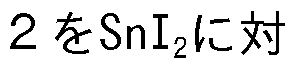
して 1 1110 添加した溶液から作製したもの, 1 . 4 11/1のスズ系ぺロブスカイ ト前 駆体溶液に還元剤
 に対して 1 (11〇 添加した溶液から作製したものを示 す。
[図 14]図 1 4は, 実施例 5における, 図面に代わる, ぺロブスカイ ト膜の断 面の 3巳1\/1写真である。 左から 0. 9 11/1のスズ系ぺロブスカイ ト前駆体溶液に還
 に対して 1 111〇 添加した溶液から作製したもの, 1 . 2 11/1のスズ系 ベロブスカイ ト前駆体溶液に還元剤
 に対して 1 1110 添加した溶液から 作製したもの, 1 . 3 11/1のスズ系べロブスカイ ト前駆体溶液に還元剤
 対して 1 1110 添加した溶液から作製したもの, 1 . 4 11/1のスズ系ぺロブスカイ ト 前駆体溶液に還元剤
 に対して 1 (11〇 添加した溶液から作製したものを 示す。
[図 15]図 1 5は, 実施例 5における太陽電池特性 (」ー カーブ) を示す, 図面に代わるグラフである。 縦軸は電流密度を示し, 横軸は電圧を示す。
[図 16-1]図 1 6— 1は, 実施例 6における還元剤 2の添加前後の様子を示す 図面に代わる写真である。 左上の写真は, 還元剤 2の添加前の溶液 (2) の 写真であり, 左下の写真は還元剤 2の添加後の溶液 (2) の写真である。 中 央上の写真は, 還元剤 2の添加前の溶液 (3) の写真であり, 中央下の写真 は還元剤 2の添加後の溶液 (3) の写真である。 右上の写真は, 還元剤 2の 添加前の溶液 (4) の写真であり, 右下の写真は還元剤 2の添加後の溶液 ( 4) の写真である。
[図 16-2]図 1 6— 2は, 実施例 6における, 図面に代わる, ぺロブスカイ ト 膜の表面 3巳!\/1写真である。 左から還元剤 2を含まないエントリ _ 1 (参照
20/175705 10 卩(:171? 2020 /008529
) , エントリ _ 2 (S n
 に還元剤 2を添加したもの) , エント リ _ 3 (3 n 2の 01^0溶液に還元剤 2を添加したもの) , 及びエントリ _ 4 ( 八〇. 7 5 1\/1八0. 2 5 3 1^ I 3の 01^0溶液に還元剤 2を添加したもの) を示す。 [図 17]図 1 7は, 実施例 6における還元剤 2を用いた場合の !_スペクトル を示す図面に代わるグラフ及びその結果をまとめたものである。 図 1 7の縦 軸は, 強度 (任意単位) であり, 横軸は波長 (〇〇〇 である。
[図 18]図 1 8は, 実施例 6における還元剤 2を用いた場合の蛍光寿命の測定 結果を示す図面に代わるグラフ及びその結果をまとめたものである。 図 1 8 の縦軸は, 強度 (任意単位) であり, 横軸は時間 (1·!秒) である。
[図 19]図 1 9は, 実施例 6における, 図面に代わる, ぺロブスカイ ト膜の表 面 3巳 IV!写真である。 左から還元剤 2を含まないエントリ _ 1 (参照) , エ ントリ _ 2 (3 n I 2の 01^0溶液に還元剤 2を添加したもの) , 及びエントリ — 4 (F A 0. 7 5 M A 0. 2 5 S n 丨 3の 01^0溶液に還元剤 2を添加したもの) を示 す。
[図 20]図 2 0は, 実施例 6における太陽電池特性 (」ー カーブ) を示す, 図面に代わるグラフである。 縦軸は電流密度を示し, 横軸は電圧を示す。
[図 21]図 2 1は, 実施例 7における還元剤 2を用いた場合の !_スペクトル を示す図面に代わるグラフ及びその結果をまとめたものである。 図 2 1の縦 軸は, 強度 (任意単位) であり, 横軸は波長 (〇〇〇 である。
[図 22]図 2 2は, 実施例 7における還元剤 2を用いた場合の蛍光寿命の測定 結果を示す図面に代わるグラフ及びその結果をまとめたものである。 図 2 2 の縦軸は, 強度 (任意単位) であり, 横軸は時間 (1·!秒) である。
[図 23]図 2 3は, 実施例 8における太陽電池特性 (」ー カーブ) を示す, 図面に代わるグラフである。 縦軸は電流密度を示し, 横軸は電圧を示す。
[図 24]図 2 4は, 実施例 8における 丨 〇巳スペクトルを示す, 図面に代わ るグラフである。 縦軸は丨 〇巳を示し, 横軸は波長 (n m) を示す。
[図 25]図 2 5は, 実施例 9における 3 n 丨 2のケミカルシフトを示す図面に代 わるグラフである。 上図は, 試料 1 (還元剤 2を添加しない状態) のものを
〇 2020/175705 1 1 卩(:171? 2020 /008529
示し, 下図は, 試料 2 (還元剤 2を添加した状態) のものを示す。
[図 26]図 2 6は, 実施例 9における 3 n 2のケミカルシフトを示す図面に代 わるグラフである。 上図は, 試料 1 (還元剤 2を添加しない状態) のものを 示し, 下図は, 試料 2 (還元剤 2を添加した状態) のものを示す。
[図 27]図 2 7は, 実施例 9において粒子が得られたことを示す図面に代わる 丁巳 IV!写真である。
[図 28]図 2 8は, 実施例 9における 3 n 丨 4のケミカルシフトを示す図面に代 わるグラフである。 上図は, 試料 1 (還元剤 2を添加しない状態) のものを 示し, 下図は, 試料 2 (還元剤 2を添加した状態) のものを示す。
[図 29]図 2 9は, 実施例 9における 3 n 丨 4及び 3 n 2を含む系のケミカル シフトを示す図面に代わるグラフである。 上図は, 試料 1 (還元剤 2を添加 しない状態) のものを示し, 下図は, 試料 2 (還元剤 2を添加した状態) の ものを示す。
[図 30]図 3 0は, 実施例 1 0における巳 3 3 丨 1~1を還元剤として用いた場合 の蛍光寿命の測定結果を示す図面に代わるグラフ及びその結果をまとめたも のである。 図 3 0の縦軸は, 強度 (任意単位) であり, 横軸は時間 (n秒) である。
[図 31]図 3 1は, 実施例 1 0における, 図面に代わる, ベロブスカイ ト膜の 表面 3巳 IV!写真である。 左から還元剤を含まない参照 ([¾ 6チ 6 r 6 n〇 6 ) , 還元剤
 丨%添加したもの, 還元剤巳 1 : 3 I 1~1を 5〇1〇 1 %添加したもの, 及び還元剤巳 1: 3 3 丨 1~1を3^2に対して 1 〇 〇 1 %添加したものを示す。
[図 32]図 3 2は, 実施例 1 0における太陽電池特性 (」 _ カーブ) を示す , 図面に代わるグラフである。 縦軸は電流密度を示し, 横軸は電圧を示す。
[図 33]図 3 3は, 八サイ ト源の影響を分析するための時間分解 !_測定結果 を示す図面に代わるグラフである。
発明を実施するための形態
[0034] 以下, 図面を用いて本発明を実施するための形態について説明する。 本発
〇 2020/175705 12 卩(:171? 2020 /008529
明は, 以下に説明する形態に限定されるものではなく, 以下の形態から当業 者が自明な範囲で適宜修正したものも含む。
[0035] 1 . ぺロブスカイ ト層の製造方法
本明細書に記載されるスズ系べロブスカイ ト層の製造方法は, 重ハロゲン化 スズを含む溶液に, 還元剤を添加し, スズ系べロブスカイ ト前駆体溶液を得 る工程を含む。 このべロブスカイ ト層の製造方法は, ぺロブスカイ ト層の製 造するための公知の工程や条件を適宜採用できる。 例えば, 方法は, スズ系 ぺロブスカイ ト化合物を含む溶液を基板に塗布する工程と, 基板に貧溶媒を 塗布する工程と, 基板をアニール処理する工程とを含んでもよい。
[0036] 還元剤
還元剤は, 例えば, スズ系ぺロブスカイ ト前駆体溶液中のフッ化スズをスズ (0価のスズ) に還元し, スズ系べロブスカイ ト前駆体溶液中の重ハロゲン 化スズをスズに還元しない還元剤である。 スズ系ぺロブスカイ ト前駆体溶液 中のフッ化スズをスズに還元するとは, 溶液中のフッ化スズ又はフッ化スズ 由来のイオンを完全に還元することまでは意味しなくてもよい。 溶液中のフ ッ化スズを, 例えば 1 %以上, 3%以上, 5%以上, 又は 10%以上, 還元できれば 良い。 重ハロゲン化スズをスズに還元しないという用語についても同様に, 重ハロゲン化スズのうち例えば 5 0 %以上, 6 0 %以上, 7 0 %以上, 8 0 %以上, 8 5 %以上, 9 0 %以上, 9 5 %以上, 又は 9 8 %以上, スズに還 元しないものであればよい。
[0037] 還元剤の酸化還元電位は, サイクリックボルタンメ トリーで酸化電位が一 1
. 8 V ド〇 〇+以下であり, より好ましくは一 0. 5 V
 ド〇 〇+である。 また, 還元剤は, シリル基を有する還 元剤であってもよい。 例えば, シリル基を基本骨格として, 又は基本骨格の 一部に含む還元剤は, 3 n 2のフッ素原子とシリル基の 3 丨原子が選択的に 反応するので, 例えば 3 n 丨 2に比べて 3 n 2と選択的に反応すると考えら れる。 シリル基を有する還元剤のうち, [ は, 蛍光寿命の延長に効果があ り, この場合も 3 n 2が _1に配位して生じる ! ! _ (ヒドリ ド) が Snを還元し
〇 2020/175705 13 卩(:171? 2020 /008529
ド〇 〇+である。 また, 還元剤は, シリル基を有する還 元剤であってもよい。 例えば, シリル基を基本骨格として, 又は基本骨格の 一部に含む還元剤は, 3 n 2のフッ素原子とシリル基の 3 丨原子が選択的に 反応するので, 例えば 3 n 丨 2に比べて 3 n 2と選択的に反応すると考えら れる。 シリル基を有する還元剤のうち, [ は, 蛍光寿命の延長に効果があ り, この場合も 3 n 2が _1に配位して生じる ! ! _ (ヒドリ ド) が Snを還元し
〇 2020/175705 13 卩(:171? 2020 /008529
ているものと考えられる。 )
[0038] 還元剤の例は, 下記式 (丨) から式 (V) で示されるいずれかの化合物で ある。
[化 6]

[0039] 式 (丨) 中,
 は, 同一でも異なってもよく, 水素原子, 又は〇1 ~
〇4アルキル基を示し,
 ◦は, 同一でも異なってもよく, 水素原子, 又は〇1 ~〇4アルキル基を示し, X !及び乂2は, 同一でも異なってもよく,
1\1又は炭素原子を示す。
式 (丨) において,
 は, 同一でも異なってもよく, 水素原子, メ チル基, 又はエチル基であり,
 ◦は, 同一でも異なってもよく, メチ ル基, 又はエチル基であることが好ましい。
[0040] 式 (丨) で示される化合物のうち, X !及び乂2が 1\1で示されるものは, 以 下の化合物 (丨 3) である。
[0041 ] [化 7]

[0042] 式 (丨
 は, 同一でも異なってもよく, 水素原子, メチル
〇 2020/175705 14 卩(:171? 2020 /008529
は, 同一でも異なってもよく, 水素原子, メチル
〇 2020/175705 14 卩(:171? 2020 /008529
基, 又はエチル基であり, ◦は, 同一でも異なってもよく, メチル基 , 又はエチル基であることが好ましい。
例えば,
 は, 全て水素原子又はメチル基であってもよいし,
2及び 3がメチル基であってもよい。

[0043] 式 (丨) で示される化合物のうち, X !が 1\1で示され, 乂2が炭素原子であ るものは, 以下の化合物 (丨 13) である。
[0044] [化 8]

[0045] 式 (丨 匕) 中,
 は, 同一でも異なってもよく, 水素原子, メチル 基, 又はェチル基であり,
 ◦は, 同一でも異なってもよく, メチル基
, 又はエチル基であることが好ましい。
例えば,
 は, 全て水素原子又はメチル基であってもよいし,
 , 2及び 3がメチル基であってもよいし,
4が水素原子であってもよい。

具体的な式 (丨 匕) で示される化合物は,
 は, 全て水素原子であり ,
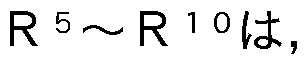 全てメチル基である化合物である。
[0046] 式 (丨) で示される化合物のうち, X !及び乂2が炭素原子であるものは, 以下の化合物 (丨 〇) である。
[0047]
〇 2020/175705 15 卩(:171? 2020 /008529
[化 9]

[0048] 式 (丨 〇) 中,
 は, 同一でも異なってもよく, 水素原子, メチル 基, 又はエチル基であり,
 ◦は, 同一でも異なってもよく, メチル基 , 又はエチル基であることが好ましい。
例えば, 例えば,
 は, 全て水素原子又はメチル基であってもよいし »


[0049] [化 10]

[0050] 式 (丨 丨) 中,
 同一でも異なってもよく, 水素原子, 又は 〇1~〇4アルキル基を示し,
 同一でも異なってもよく, 水 素原子, 又は〇1~〇4アルキル基を示し, 乂3及び乂4は, 同一でも異なって もよく, 1\1又は単結合を示す。
式 (丨 丨) において, [¾1 1~[¾18は, 同一でも異なってもよく, 水素原子 メチル基又はェチル基を示し, は, 同一でも異なってもよく,
〇 2020/175705 16 卩(:171? 2020 /008529
水素原子, メチル基又はエチル基を示し, 乂3及び乂4は, 同一でも異なって もよく, 1\1又は炭素原子を示すものが好ましい。
[0051] 式 (丨 丨) で示される化合物のうち, 乂3及び乂4が 1\1で示されるものは, 以下の式 (丨 丨 3) で示される。
[0052] [化 11]

[0053] 式 (丨 丨 3) で示される具体的な化合物は,
 が水素原子であり , がメチル基の化合物である。
[0054] [化 12]
 1 )
1 )
[0055] 式 (丨 丨 丨) 中, [¾31~[¾34は, 同一でも異なってもよく, 水素原子, 〇! ~〇4アルキル基, 〇2~〇4アルケニル基, 〇2~〇4アルキニル基, 〇1~〇 4アルコキシ基, 〇 1~〇4アルキルチオ基, アリール基, アリールオキシ基, 又はアリールチオ基を示す。
[0056] 上記において, アリール基は, 例えば炭素数 6_ 1 2のアリール基であり , アリール基の例は, ベンジル基又はフエニル基であり, アリールオキシ基 は, 例えば炭素数 6 -2のアリールオキシ基であり, アリールオキシ基の例 は, フエノキシ基である。 アリールチオ基は, 例えば, 炭素数 6- 1 2のア リールチオ基である。 〇2~〇4アルケニル基は, 炭素数が 2〜 4の直鎖状又
\¥02020/175705 17 卩(:17 2020 /008529
は分岐側鎖を有するアルケニル基である。 〇2~〇4アルケニル基の例は, ビ ニル基, プロべニル基, 及びブテニル基等である。 〇2~〇4アルキニル基は , 炭素数が 2〜 4の直鎖状又は分岐側鎖を有するアルキニル基である。 〇2〜 〇4アルキニル基の例は, エチニル基及びプロピニル基である。
以下同様である。
[0057] 式 ( I I I) において,
[¾ 3 1〜[¾ 34のすべてが水素原子以外のもの (例えばメチル基, 又はエチル基 ) であってもよいし,
[¾31〜[¾34のうち ]つが水素原子で, 残りが 〇1~〇4アルキル基, 〇1~〇 4アルコキシ基, 〇 1~〇4アルキルチオ基, アリール基, アリールオキシ基, 又はアリールチオ基であってもよい。
[0058] 式 (丨 丨 丨) において, [¾31が水素原子であり, [¾32~[¾34がエチル基で ある化合物は, 巳 133 丨 1~1である。
[0059] [化 13]

[0060] 式 (丨 V) 中, [¾35〜[¾37は, 同一でも異なってもよく, 水素原子, 〇1~ 〇4アルキル基, 〇2~〇4アルケニル基, 〇2~〇4アルキニル基, 〇1~〇4 アルコキシ基, 〇 1 ~〇4アルキルチオ基, アリール基, アリールオキシ基, 又はアリールチオ基を示し,
乂5は, ハロゲン原子を示す。
式 (丨 V) において,
[¾ 35〜[¾ 37のすべてが水素原子以外のもの (例えばメチル基, 又はエチル基 ) であってもよい。 ハロゲン原子の例は, 重ハロゲン原子 (塩素原子, 臭素 原子及びヨウ素原子) である。
[0061]
\¥02020/175705 18 卩(:17 2020 /008529
[化 14]

[0062] 式 (V) 中,
 同一でも異なってもよく, 水素原子, 〇1~〇 4アルキル基, 〇2~〇4アルケニル基, 〇2~〇4アルキニル基, 〇1~〇4ア ルコキシ基, 〇1〜〇4アルキルチオ基, アリール基, アリールオキシ基, 又 はアリールチオ基を示す。
[0063] 式 (V) において,
 のすべてが水素原子以外のもの (例えばメ チル基, 又はエチル基) であってもよいし, [¾41~[¾46のうち 1つが水素原 子で, 残りが水素原子以外のもの (例えばメチル基, 又はエチル基) であっ てもよい。
[0064] 還元剤は, 基本的には, スズ系ぺロブスカイ ト前駆体溶液中のフッ化スズ をスズに還元し, スズ系ぺロブスカイ ト前駆体溶液中の重ハロゲン化スズを スズに還元しないものであり, 上記式 (丨) から式 (V) で示されるいずれ かの化合物で表される還元剤に限られない。 また, 還元剤は, 成膜工程にお いて, 層中に残留しないか, 残留しても, ぺロブスカイ ト層に悪影響を与え ない, 又は微量に残留することがかえって, ぺロブスカイ ト層の特性を向上 させるものであることが好ましい。 上記の通り, 式 (1) から式 (V) で示 される化合物は, そのような望ましい特性を有する, 本発明の還元剤である 。 これと同様の観点から, 以下の化合物も, 本発明の還元剤として有効であ ると考えられる。
[0065] ゲルマニウム系還元剤
ゲルマニウ厶系還元剤の例は, 〇6 2, 060 I 2» 〇6巳 1"2, 06 I 2 , 0 © 0 , 0 © ? , 0 © 3 , 0 © I 4 » 及び 0 © 0 I 4である。
[0066] ボラン系還元剤
ボラン系還元剤の例は,
 〇 2020/175705 19 卩(:171? 2020 /008529
[0067] アルミニウム系還元剤
アルミニウム系還元剤の例は, 0 丨 BAL_H (水素化ジイソプチルアルミ ニウム) 及び 1_八1~1 (水素化アルミニウムリチウム) である。
[0068] 上記以外の還元剤の例は, ナフタセノ [5,
 : 1 1 , 1 2 -〇,
, 〇1’ ] ビス [1 , 2] ジチオール

[1,2] 丨〇16) :〇八番号 1 93 -44 - 2又は, その誘導体 (例えば, こ の化合物の環の 1又は複数の水素原子がアルキル基又はアルコキシ基により 置換されたもの, この環の一部の炭素原子が, 窒素原子又は硫黄原子で置換 されたもの) である。
[0069] 重ハロゲン化スズ
重ハロゲン化スズを含む溶液 (スズ系べロブスカイ ト前駆体溶液) の例は , スズ系べロブスカイ ト層を作成するための前駆体を含む溶液 (スズ系べ口 ブスカイ ト前駆体溶液) である。 この溶液は, 例えば不純物として, フッ化 スズを含む。 フッ化スズの含有量は, 通常微量である。 重ハロゲン化スズは , ヨウ化スズ, 臭化スズおよび塩化スズから選ばれる 1種又は 2種以上を含 む。
[0070] ぺロブスカイ ト層に用いられるスズ系ぺロブスカイ ト化合物自体は公知で あり, 本明細書においても, 3
 (スズ) を含むスズ系ぺロブスカイ ト化合 物を適宜用いることができる。 重ハロゲン化スズは, 例えば, S n Xml (X は 丨, 巳 「, 〇 丨のいずれか 1種以上であり, 1は, ·! . 8£〇11 £ 2
. 2) で示される。 重ハロゲン化スズは, ヨウ化スズを含むものが好ましい 。 重ハロゲン化スズは, ヨウ化スズ, 臭化スズおよび塩化スズを含むもので あってもよい。 例えば, 重ハロゲン化スズは, ヨウ化スズおよび臭化スズか ら主に構成される。 スズ系ぺロブスカイ ト前駆体溶液において, 重ハロゲン 化スズは, イオンとして電離した状態で存在していてもよい。
[0071] 重ハロゲン化スズは, 式 (V 丨) で示されるスズ系べロブスカイ ト化合 物 (本発明のぺロブスカイ ト化合物ともよぶ) であってもよい。

[式中, 3 nの酸化数は 1. 5〜 4である。
 は少なくとも 1種の 1価のカチ オンを示す。 Xは少なくとも 1種の重ハロゲン原子を示す。 』は 2. 5〜 3.
5を示す。 ]
3门の酸化数は 1. 5〜 3. 5であることが好ましく 1. 5〜 2. 5でも よいし, 1. 8~2. 2でもよいし, 1. 5〜 2でもよい。
[0072] —般式 (V 丨) において, は少なくとも 1種の 1価のカチオンである。
 は 2種以上のカチオンであってもよい。 このような 1価のカチオンの例は, アルカリ金属カチオンや 1価の遷移金属カチオンである。
[0073] アルカリ金属カチオンの例は, ナトリウムカチオン, カリウムカチオン, セシウムカチオン, ルビジウムカチオンである。
[0074] 1価の遷移金属カチオンの例は, 銅カチオン, 銀カチオン, 金カチオン, 鉄 カチオン, ルテニウムカチオンである。
[0075] の具体的な例は, [¾511\! 1~13+である示されるカチオン ([¾51は 1価の置 換又は非置換の炭化水素基を示す。 ) である。 置換の炭化水素基は, 炭化水 素基の水素原子が他の原子又は置換基によって置換された炭化水素を意味す る。 8の別の具体的な例は,
[0076] ^2 + = 0 ( 2) - 1\11~12
[0077] (?¾42は水素原子又は 1価の置換若しくは非置換炭化水素基を示す。 )
で表されるカチオンである。
[0078] 本明細書において, 「1価の炭化水素基」 の例は, アルキル基, アリール基 又はアラルキル基である。
[0079] アルキル基は, 炭素数 1〜 20の直鎖状, 分岐状又は環状アルキル基が好ま しい。 アルキル基の具体例は, メチル基, エチル基,
 プロピル基, 2—プ ロピル基, 门ーブチル基, 1—メチルプロピル基, 2—メチルプロピル基, 16 —ブチル基,
 ペンチル基, 1—メチルブチル基, 1—エチルプロピル基, 士6 「1:_ペンチル基, 2—メチルブチル基, 3—メチルブチル基, 2,2—ジメチルプ ロピル基,
 ヘキシル基, 1—メチルペンチル基, 1—エチルブチル基, 2— メチルペンチル基, 3—メチルペンチル基, 4—メチルペンチル基, 2—メチル
〇 2020/175705 21 卩(:171? 2020 /008529 ペンタンー 3—イル基, 3, 3—ジメチルブチル基, 2, 2—ジメチルブチル基, 1,
ヘキシル基, 1—メチルペンチル基, 1—エチルブチル基, 2— メチルペンチル基, 3—メチルペンチル基, 4—メチルペンチル基, 2—メチル
〇 2020/175705 21 卩(:171? 2020 /008529 ペンタンー 3—イル基, 3, 3—ジメチルブチル基, 2, 2—ジメチルブチル基, 1,
1—ジメチルプチル基, 1 , 2—ジメチルプチル基, 1 , 3—ジメチルプチル基, 2, 3—ジメチルブチル基, 1—エチルブチル基, 2—エチルブチル基,
 ヘプチ ル基, 门ーオクチル基, n—ノニル基, n—デシル基, 门ーウンデシル基, n—ド デシル基,
 トリデシル基, n _テトラデシル基,
 ペンタデシル基,
 へキサデシル基, n _ヘプタデシル基, n _オクタデシル基, n _ノナデシル基 , 门ーイコシル基, シクロプロピル基, シクロブチル基, シクロペンチル基, シクロヘキシル基である。
[0080] 「アリール基」 は, 炭素数 6〜 20のアリール基が好ましい。 アリール基の例 は, フエニル基, インデニル基, ペンタレニル基, ナフチル基, アズレニル 基, フルオレニル基, フエナントレニル基, アントラセニル基, アセナフチ レニル基, ビフエニレニル基, ナフタセニル基, ピレニル基である。
[0081 ] 「アラルキル基」 は, 炭素数 7〜 20のアラルキル基が好ましい。 アラルキル 基の例は, ベンジル基, フエネチル基, 1—フエニルプロピル基, 2—フエニ ルプロピル基, 3—フエニルプロピル基, 1—フエニルプチル基, 2—フエニル プチル基, 3—フエニルプチル基, 4—フエニルプチル基, 1—フエニルペンチ ルプチル基, 2—フエニルペンチルプチル基, 3—フエニルペンチルプチル基 , 4—フエニルペンチルプチル基, 5—フエニルペンチルプチル基, 1—フエニ ルヘキシルブチル基, 2—フエニルヘキシルブチル基, 3—フエニルヘキシル ブチル基, 4—フエニルヘキシルブチル基, 5—フエニルヘキシルブチル基, 6 —フエニルヘキシルブチル基, 1—フエニルへプチル基, 1—フエニルオクチ ル基, 1—フエニルノニル基, 1—フエニルデシル基, 1—フエニルウンデシル 基, 1—フエニルドデシル基, 1—フエニルトリデシル基, 1—フエニルテトラ デシル基である。
[0082] 「置換基」 の例は, 上記した 1価の炭化水素基, ハロゲン原子 (例えば, フ ツ素原子, 塩素原子, 臭素原子, ヨウ素原子) , _〇 ( は水素原子又は上 記 1価の炭化水素基を示す) , 一3(^ ((^は水素原子又は上記 1価の炭化水素基 を示す) , ニトロ基, アミノ基, シアノ基, スルホ基, カルボキシ基, カル
〇 2020/175705 22 卩(:171? 2020 /008529
バモイル基, アミノスルホニル基, オキソ基である。 置換基を有する場合の 置換基の数は, 特に限定されず, 10以下が好ましく, 5以下がより好ましく,
3以下がさらに好ましい。
[0083]
 本発明のぺロブスカイ ト化 合物が三次元構造を有しやすく, より広い波長域で光を吸収し, エネルギー 変換効率 ( 〇£) 及び内部量子効率 (1(^) を向上させやすい観点から, 炭素 数 1〜 10のアルキル基, 炭素数 6〜 20のアリール基及び炭素数 7〜 12のアラルキ ル基が好ましく, 炭素数 1〜 6のアルキル基及び炭素数 6〜 14のアリール基がよ り好ましく, 炭素数 1〜 4のアルキル基がさらに好ましい。 また, 同様の理由 により, 1^51及び 2としては, アルキル基が好ましく, 直鎖状又は分岐状ア ルキル基がより好ましく, 直鎖状アルキル基がさらに好ましい。 特に, メチ ル基が最も好ましい。
[0084] 上記(¾51及び(¾52としては, 本発明のぺロブスカイ ト化合物が三次元構造を 有しやすく, より広い波長域で光を吸収し, エネルギー変換効率 ( 〇£) 及び 内部量子効率 (1(^) を向上させやすい観点から, (¾51はメチル基が好ましく , 52は水素原子が好ましい。 つまり, としては, アルカリ金属カチオンや 1 価の遷移金属カチオンの他には, (^3 3 +又は以下のカチオンであることが好ま しい。

. 4以下が好ましく, 〇. 2以上〇. 3以下でもよい) で示される基である
[0087] —般式 (丨 丨) において, エネルギー変換効率 0£) 及び内部量子効率 ( 1(^) を向上させやすい観点から, 」は, 2. 8〜 3. 2が好ましい。
[0088] このような条件を満たす本発明のぺロブスカイ ト化合物の例は, ヨウ化ス ズメチルアンモニウム (〇 1~131\11~133门 丨 3 : 「1\/1八 3门 丨 3」 と略記) , (
 23 |^3 丨 8 : 「1\/1八23 |^3 丨 8」 と略記, 臭化スズメチルアンモ
〇 2020/175705 23 卩(:171? 2020 /008529
23 |^3 丨 8 : 「1\/1八23 |^3 丨 8」 と略記, 臭化スズメチルアンモ
〇 2020/175705 23 卩(:171? 2020 /008529
ニウム (〇1~131\11~133门巳 「3 : 「1\/1八3门巳 「3」 と略記) , ヨウ化スズホ ルムアミジニウム ( (1\11~12) 2〇 1~13 n 丨 3 : 「 八3 n 丨 3」 と略記) , 及 び臭化スズホルムアミジニウム ( (1\11~12) 2〇1~13门巳 「3 : 「 八3门巳 「 3」 と略記) ,
 〇〜 1の数であり, 0. 1以上 0. 4以 下が好ましく, 〇. 2以上〇. 3以下でもよい)

らの混合物である。 これらの中では, ド八0.751^0.2 13, 1\/1八3 |^ 丨 3及び 八3 丨 3が好ましい。
[0089] 以下の実施例では, 微量のフッ化スズを含む重ハロゲン化スズを用いたぺ ロブスカイ ト層の製造方法を中心として, 説明されている。 一方, 上記の還 元剤は, 例えば, AS n X3型といった, 様々なスズ系べロブスカイ ト層にお いても, フッ化スズ由来のスズのナノパーテイクルによるスカベンジャーの 効果が期待される。
[0090] スズ系ぺロブスカイ ト化合物を含む溶液は, 基本的には, ハロゲン化スズ
, ハロゲン化されたカチオン源となる化合物を溶媒に溶解させることで得る ことができる。 溶媒は, 極性溶媒であることが好ましく, 非プロトン性の極 性溶媒であることがより好ましい。 ハロゲン化されたカチオン源となる化合 物の例は, 八 丨, 1\/1八 丨, 八巳 「, 1\/1八巳 「,
 ド八] - 八 巳 「及びこれらの混合物である。 ハロゲン化スズとハロゲン化されたカチオン 源となる化合物とのモル比は, 1 : 3以上 3 : 1でもよく, 1 : 2〜 2 : 1 でもよく, 3 : 2〜 2 : 3でもよく, 3 : 4〜 4 : 3でもよい。
[0091] 溶媒は, 沸点が 35〜 250°〇程度の溶媒が好ましい。 溶媒の例は, 1\1, 1\1_ジ メチルホルムアミ ド 1^) , ジメチルスルホキシド 1^0) , スルホラン,
1\1—メチルピロリ ドン, プロピレンカーボネート, 《—アセチルー· —プチ ロラクトン, テトラメチレンスルホキシド, エチルシアノアセテート, アセ チルアセトン, 3—メ トキシ
 1\1, ‘ージメチ ルエチレンウレア, 1, 1,3, 3—テトラメチルウレア, 2—アセチルシクロヘキ サノン, 1,3 -ジメチルー 3, 4, 5, 6 -テトラヒドロー 2(1 -ピリミジノン, 3, 4—ジヒドロー 1(2 —ナフタレノン, シクロペンタノン, シクロへキサノン
〇 2020/175705 24 卩(:171? 2020 /008529
1\1, ‘ージメチ ルエチレンウレア, 1, 1,3, 3—テトラメチルウレア, 2—アセチルシクロヘキ サノン, 1,3 -ジメチルー 3, 4, 5, 6 -テトラヒドロー 2(1 -ピリミジノン, 3, 4—ジヒドロー 1(2 —ナフタレノン, シクロペンタノン, シクロへキサノン
〇 2020/175705 24 卩(:171? 2020 /008529
, シクロへプタノン, アニリン, ピぺリジン, ピリジン, 4_ 6 _プチルビ リジン, 4—アミルピリジン, 4—アミノピリジン, 2—アミルピリジン, 4— メチルピリジン, ペンタフルオロピリジン, 2, 4, 6—テトラメチルピリジン,
2, 6—ジ _ 6 ーブチルー 4—メチルピリジン, 4—ピリジンエチルアミン, シ クロオクタノン, 2, 5—ジメ トキシテトラヒドロフラン, 1 , 4, 7, 10—テトラオ キサシクロドデカン, エチル トルエート, 1 , 2—ジメ トキシベンゼン, テ トラヒドロフルフリルアセテート, シクロヘキシルアセテート, シクロペン チルメチルエーテル, フエニルエチルアミン, エチレンジアミン, トリエチ ルアミン, ジイソプロピルエチルアミン, ヒドラジン等が挙げられる。 なか でも, 金属中心に配位結合を形成するという観点から,
 -ジメチルホルム アミ ド 1^) 又はジメチルスルホキシド 1^0) が好ましい。
[0092] 溶媒中におけるハロゲン化スズの濃度の例は, 〇. 1 ~ 5〇1〇 1 / 1_ (又 は〇. 5 ~ 3〇1〇 丨 / 1_) である。 スズ系ぺロブスカイ ト化合物を含む溶液 は, 上記の溶媒に, 上記した化合物を適宜混合することにより得ることがで きる。 また, 必要に応じて, 溶媒を適宜攪拌及び加熱し, 化合物を溶解すれ ばよい。
[0093] 基板
基板として, ベロブスカイ ト型太陽電池や有機巳 1_素子における公知の基 板を適宜用いることができる。 基板の例は, ガラス基板, 絶縁体基板, 半導 体基板, 金属基板及び導電性基板 (導電性フィルムも含む) である。 また, これらの表面の一部又は全部の上に, 金属膜, 半導体膜, 導電性膜及び絶縁 性膜の少なくとも 1種の膜が形成されている基板も好適に用いることができる
[0094] 金属膜の構成金属の例は, ガリウム, 鉄, インジウム, アルミニウム, バ ナジウム, チタン, クロム, ロジウム, ニッケル, コバルト, 亜鉛, マグネ シウム, カルシウム, シリコン, イッ トリウム, ストロンチウム及びバリウ ムから選ばれる 1種又は 2種以上の金属である。 半導体膜の構成材料の例は, シリコン, ゲルマニウム等の元素単体, 周期表の第 3族〜第 5族, 第 13族〜第 1
〇 2020/175705 25 卩(:171? 2020 /008529
5族の元素を有する化合物, 金属酸化物, 金属硫化物, 金属セレン化物, 金属 窒化物等が挙げられる。 また, 導電性膜の構成材料の例は, スズドープ酸化 インジウム (1丁0) , フッ素ドープ酸化インジウム 丁〇) , 酸化亜鉛 (å门0)
, アルミニウムドープ酸化亜鉛 (八å0) , ガリウムドープ酸化亜鉛 (0å0) , 酸化スズ ^2) , 酸化インジウム (1¾03) , 酸化タングステン (1«03) であ る。 絶縁性膜の構成材料の例は, 酸化アルミニウム (八1203) , 酸化チタン (丁 |〇2) , 酸化シリコン 102) , 窒化シリコン ⑸ ) , 酸窒化シリコン 〇 51\13) である。
[0095] 基板の形状の例は, 平板や円板等の板状, 繊維状, 棒状, 円柱状, 角柱状 , 筒状, 螺旋状, 球状, リング状であり,多孔質構造体であてもよい。 これら のうちでは板状の基板が好ましい。 基板の厚さの例は, 0 . 1 ~ 1 0 0 01〇!が好ましく, 1 01 ~ 1 0 01 01がより好ましい。
[0096] スズ系べロブスカイ ト化合物を含む溶液を基板に塗布する工程
スズ系べロブスカイ ト化合物を含む溶液を基板に塗布する際に, 基板には , 下地層である半導体層が形成されている場合がある。 その場合, スズ系べ ロブスカイ ト化合物を含む溶液を基板に塗布するとは, 下地層が形成された 基板に (の下地層の上に) スズ系べロブスカイ ト化合物を含む溶液を塗布す る工程を意味する。
[0097] スズ系べロブスカイ ト化合物を含む溶液を基板に塗布するためには, スピ ンコート, ディップコート, スクリーン印刷法, 口ールコート, ダイコート 法, 転写印刷法, スプレー法, 又はスリッ トコートを用いればよい。 これら の中では, スピンコートにより基板上に溶液を塗布することが好ましい。 ス ビンコートは, 基板を回転させつつ, 溶液を滴下し, 基板上に溶液を塗布す る方法である。 また, 溶液を搭載した基板を回転させ, 基板に溶液を塗布し てもよい。 回転速度は, 最大速度が 1 0 0 0〜 1万「 を 3 0秒から 5分 , 最高速度までを 2秒から 1 5秒, 最大速度から停止までを 1秒から 1 5秒 とすればよい。
[0098] 次に, 基板に貧溶媒を塗布する工程について説明する
〇 2020/175705 26 卩(:171? 2020 /008529
[0099] 貧溶媒とは, 溶質を溶かす能力はあるものの, 溶質の溶解度が高くない溶媒 を意味する。 貧溶媒の例は, ジクロロメタン, クロロホルム等の置換脂肪 族炭化水素; トルエン, ベンゼン等の芳香族炭化水素; クロロベンゼン, 才 ルトジクロロベンゼン, ニトロベンゼン等の置換芳香族炭化水素;酢酸;ジ エチルエーテル, テトラヒドロフラン (丁#) 等のエーテル; メタノール, エ タノール, イソプロパノール, ブタノール, オクタノール等のアルコール; ヘキサン等の長鎖炭化水素 (特に 0 4 - 1 0炭化水素) ; ァセトニトリル等 が挙げられる。 これら貧溶媒は, 単独で使用することもできるし, 2種以上を 組合せて使用することもできる。 これらの中では, クロロベンゼン又はトル エンが好ましい。
[0100] 貧溶媒は, 単独でも, 極性溶媒と混合して用いられてもよい。 貧溶媒が極 性溶媒と混合される場合, 極性溶媒と, 貧溶媒との比が, 貧溶媒/極性溶媒 = 2. 0〜 10. 0/1 . 0 (体積比) が好ましく, 3. 0〜 8. 0/1 . 0 (体積比) がより好 ましい。
[0101 ] 貧溶媒を塗布する際には, スズ系べロブスカイ ト化合物が基板に塗布され ているので, 基板に貧溶媒を塗布するとは, スズ系ぺロブスカイ ト化合物が 塗布されている状態の基板に貧溶媒を塗布することを意味する。 基板に貧溶 媒を塗布する方法は, スズ系ぺロブスカイ ト化合物を塗布する方法と同様で ある。 なお, スズ系ぺロブスカイ ト化合物をスピンコート塗布している際に , 貧溶媒を基板に滴下して, 貧溶媒を基板に塗布してもよい。 塗布される貧 溶媒の量は適宜調整すればよい。 スズ系ぺロブスカイ ト化合物を含む溶液と 貧溶媒の体積比は, 1 : 1 〇〜 2 : 1でもよいし, 1 : 5〜 1 : 1でもよい
[0102] 基板に貧溶媒を塗布する際の貧溶媒の温度が 4 5 °〇以上 1 0 0 °〇以下であ ることが好ましい。 後述する実施例により示された条件のもとでは, この温 度の貧溶媒を用いる場合には, 種結晶からの結晶成長を抑制し, 種結晶の形 成を促進できるので, その結果, スズ系ぺロブスカイ ト層を充填させ, スズ 系べロブスカイ ト層の凹凸を軽減し, 平坦で抜けのないスズ系べロブスカイ
〇 2020/175705 27 卩(:171? 2020 /008529
卜層を得ることができる。 この方法は, 貧溶媒の温度が 4 5 °〇以上 8 5 °〇以 下であってもよいし, 5 0 °〇以上 7 0 °〇以下であってもよい。 この温度であ れば, 下地層を傷つけずにスズ系べロブスカイ ト化合物を成長させることが できる。 貧溶媒の温度は, スズ系ぺロブスカイ ト化合物の種類等に応じて適 宜調整すればよい。
[0103] 貧溶媒は, 基板を回転しつつ貧溶媒を滴下することにより塗布され, 貧溶 媒が塗布された後 0 . 5秒以上 7 . 5秒以内 (例えば, 1秒以上 7秒以下,
1秒以上 6秒以下) に回転が停止するものが好ましい。 後述する実施例によ り実証された通り, 貧溶媒を滴下後, 極めて迅速に回転を停止させることで , スズ系ぺロブスカイ ト化合物の状態を調整できることとなる。 また, 従来 , 通常貧溶媒を滴下後 3 0秒程度回転速度を維持した後に, 基板の回転を減 速させていた。 本明細書においては, 後述する実施例により示された通り, 貧溶媒の滴下完了直後〜 1 〇秒以内 (直後から 5秒以内, 直後から 3秒以内 , 直後から 2秒以内, 直後から 1秒以内, 又は直後) に, 基板の回転速度を 減速し始めることが好ましい。 このようにすることで, ぺロブスカイ ト層 ( 膜) 内での特性のばらつきを抑えることができる。
[0104] なお, スズ系ぺロブスカイ ト化合物を含む溶液を塗布する工程や, 貧溶媒 を塗布する工程においては, 後述するアニール処理工程と同様, 密閉系で行 うことが好ましい。 そして, 密閉系では, スズ系べロブスカイ ト化合物を含 む溶液に含まれる溶媒の蒸気が存在することが好ましく, さらに好ましくは , 密閉系内ではその溶媒が飽和蒸気圧又は飽和蒸気圧の 9 0 %以上の分圧と なっていることが好ましい。
[0105] 次に, 基板をアニール処理する工程について説明する。 アニール処理とは, 基板を加熱等する工程を意味する。 アニールエ程は, 貧溶媒の滴下後, 又は 基板が停止した後, 速やかに行うことが好ましい。 アニール処理する工程は , 後述する実施例により示された通り, 溶媒蒸気を含む密閉系にて, 段階的 に基板加熱する工程を含むものが好ましい。 そして, 密閉系では, スズ系べ ロブスカイ ト化合物を含む溶液に含まれる溶媒の蒸気が存在することが好ま
〇 2020/175705 28 卩(:171? 2020 /008529
しく, さらに好ましくは, 密閉系内ではその溶媒が飽和蒸気圧又は飽和蒸気 圧の 9 0 %以上の分圧となっていることが好ましい。
[0106] 基板をアニール処理する工程は, 2段又はそれ以上の段階で温度を上昇さ せることが好ましい。 そのように多段で温度を上昇させることで, 実施例に より実証された通り, スズ系べロブスカイ ト化合物の成長を促し, 粒子サイ ズを大きくすることができ, それによりスズ系べロブスカイ ト層を充填させ ることができる。
[0107] アニール処理が多段階を含む場合とは, 目標となる複数の温度まで基板温 度を上昇させた後, その設定温度で所定時間維持し, その後次の設定温度ま で基板温度を上昇させることを意味する。
第 1段の設定温度の例は, 3 0 °〇以上 6 0 °〇以下であり, 3 5 °〇以上 5 5 °〇以下でもよいし, 4 0 °0以上 5 0 °0以下でもよい。
第 1段の設定温度の滞留時間は, 5秒以上 1分以下でもよいし, 5分以上
2 0分以下でもよい。
第 2段の設定温度は, 第 1段の設定温度より高いことが好ましい。 第 2段 の設定温度の例は, 5 0 °〇以上 8 0 °〇以下であり, 5 5 °〇以上 7 5 °〇以下で もよいし, 6 0 °◦以上 7 0 °◦以下でもよい。
第 2段の設定温度の滞留時間は, 5秒以上 1分以下でもよいし, 5分以上
3 0分以下でもよいし, 5分以上 2 0分以下でもよいし, 1 0分以上 2 0分 以下でもよい。
第 3弾の設定温度 (第 1段又は第 2段を省略した場合は, 第 2段の設定温 度) は, 第 1段又は第 2段の設定温度より高いものが好ましい。 第 3段の設 定温度の例は, 7 0 °〇以上 1 2 0 °〇以下であり, 8 0 °〇以上 1 1 0 °〇以下で もよいし, 9 0 °◦以上 1 1 0 °◦以下でもよい。
第 3段の設定温度の滞留時間は, 5秒以上 1分以下でもよいし, 5分以 上 2 0分以下でもよい。
このようにして, ぺロブスカイ ト層を得ることができるぺロブスカイ ト 層の膜厚の例は, 1 〇 01以上 1 0 0 0 〇!以下である。 膜厚は, 5 0门〇!
〇 2020/175705 29 卩(:171? 2020 /008529
以上 5 0 0 01以下でもよいし,
 以下でもよいし
,
 以下でもよい。
[0108] 上記のベロブスカイ ト層の製造方法によりべロブスカイ ト層を得た後, 通常 の方法に従って, ぺロブスカイ ト型太陽電池を製造できる。 もっとも, ぺ口 ブスカイ ト層は, 有機巳 !_素子の製造にも用いることができるため, 上記の ぺロブスカイ ト層の製造方法によりべロプスカイ ト層を得た後に, そのぺ口 ブスカイ ト層を用いて有機巳 !_素子を製造できる。
[0109] 本明細書に記載される次の発明は, ぺロブスカイ ト層及びそのべロプスカ イ ト層を含むぺロブスカイ ト型太陽電池に関する。 そのべロブスカイ ト層は , スズ系ぺロブスカイ ト化合物を含み, スズ系ぺロブスカイ ト化合物による 被覆率が 9 5 %以上 1 0 0 %以下であることが好ましい。 被覆率は 9 8 %以 上 1 0 0 %以下がより好ましく, 9 9 %以上 1 0 0 %以下がより好ましい。 もっとも, 特性を損なわない限り, 被覆率が 9 5 %以上 1 0 0 %であっても , 従来技術に基づいて製造した場合に比べて被覆率が高まるので好ましい。 このべロブスカイ ト層は, スズ系べロブスカイ ト化合物の平均粒子径が 1 5
 以下であることが好ましい。 被覆率は, 3巳 IV!画像を 撮影し, その面積から算出すればよい。 具体的に説明すると, 画像解析ソフ 卜を用いて被覆率を求めてもよいし, ぺロブスカイ ト化合物が覆っておらず 黒くなっている領域を取り囲み, 取り囲んだ部分の面積を求めることで, ぺ ロブスカイ ト化合物が基板を覆っている面積の割合である被覆率を求めても よい。 また, スズ系ぺロブスカイ ト化合物の平均粒子径もスズ系ぺロプスカ イ ト層を撮影し, スズ系べロブスカイ ト化合物境界面を用いて, 平均となる 大きさ (例えば, 境界面の最大長さの平均値) を求めればよい。 平均粒子径 は, 算術平均値を採用すればよい。
[01 10] 2 . ぺロブスカイ ト型太陽電池
ぺロブスカイ ト型太陽電池は, 例えば, 透明電極, (正孔) ブロッキング 層, 電子輸送層, ぺロブスカイ ト層 (光吸収層) , 正孔輸送層, 及び金属電 極をこの順に備える。 ぺロブスカイ ト型太陽電池は, 透明電極上に〇型半導
〇 2020/175705 30 卩(:171? 2020 /008529
体層が設けられた順型であってもよいし, 透明電極上に 型半導体層が設け られた逆型であってもよい。 以下に, 透明電極, (正孔) ブロッキング層, 電子輸送層, ぺロブスカイ ト層 (光吸収層) , 正孔輸送層, 及び金属電極を この順に備えるぺロブスカイ ト型太陽電池を例にして, ぺロブスカイ ト型太 陽電池を説明する。
[01 1 1 ] 2 . 1 . 透明電極
透明電極は, 電子輸送層の支持体であるとともに, (正孔) ブロッキング 層を介してべロブスカイ ト層 (光吸収層) より電流 (電子) を取り出す機能 を有する層であることから, 導電性基板が好ましく, 光電変換に寄与する光 を透過可能な透光性を有する透明導電層が好ましい。
[01 12] 透明導電層としては, 例えば, スズドープ酸化インジウム (丨 丁〇) 膜, 不純物ドープの酸化インジウム (丨 门2〇3) 膜, 不純物ドープの酸化亜鉛 ( Z n〇) 膜, フッ素ドープニ酸化スズ ( 丁〇) 膜, これらを積層してなる 積層膜等が挙げられる。 これら透明導電層の厚みは特に制限されず, 通常, 抵抗が 5〜 1 5 0 /□ (単位面積当たり) となるように調整することが好ま しい。 当該透明導電層は, 成形する材料に応じ, 公知の成膜方法により得る ことができる。
[01 13] 透明導電層は, 外部から保護するために, 必要に応じて, 透光性被覆体に より覆われ得る。 当該透光性被覆体としては, 例えば, フッ素樹脂, ポリ塩 化ビニル, ポリイミ ド等の樹脂シート ; 白板ガラス, ソーダガラス等の無機 シート ; これらの素材を組合せてなるハイブリッ ドシート等が挙げられる。 これら透光性被覆体の厚みは特に制限されず, 通常, 抵抗が 5〜 1 5 0 /0 となるように調整することが好ましい。
[01 14] 2 . 2 . (正孔) ブロッキング層
(正孔) ブロッキング層は, 正孔の漏れを防ぎ, 逆電流を抑制して太陽電 池特性 (特に光電変換効率) を向上させるために設けられる層であり, 透明 電極とぺロブスカイ ト層 (光吸収層) との間に設けられることが好ましい。
(正孔) ブロッキング層は, 酸化チタン等の金属酸化物からなる層が好まし
〇 2020/175705 31 卩(:171? 2020 /008529
く, コンパクト丁 丨 〇2等の 型半導体で透明電極の表面を平滑且つ緻密に覆 った層がより好ましい。 「緻密」 とは, 電子輸送層中の金属化合物の充填密 度より高密度で金属化合物が充填されていることを意味する。 なお, 透明電 極と電子輸送層とが電気的に接続されなければ, ピンホール, クラック等が 存在していてもよい。
[0115] (正孔) ブロッキング層の膜厚は, 例えば, 5〜 300 である。 (正孔) ブ ロッキング層の膜厚は, 電極への電子注入効率の観点より, 10〜 200 がより 好ましい。
[0116] (正孔) ブロッキング層は上記透明電極上に形成される。 金属酸化物を ( 正孔) ブロッキング層に用いる場合, 既知の方法に従って (例えば, 非特許 文献 4, 丄 卩 .
 卩 . 2008, 41, 102002.等) , スプレーパイロ リシスを行うことにより作製できる。 例えば, 200〜 550°〇 (特に 300〜 500°〇 ) に加熱したホッ トプレート上に置いた透明電極に 0.01〜 0.4011/1 (特に 0.02〜 0.2011/1) の金属アルコキシド (チタンジ (イソプロポキシド) ビス (アセチル アセトナート) 等のチタンアルコキシド等) のアルコール溶液 (例えばイソ プロピルアルコール溶液等) をスプレーで吹き付けて作製できる。
[0117] その後, 得られた基板を, 酸化チタン (丁 丨 〇2等) , チタンアルコキシド (チタンイソプロポキシド等) , チタンハロゲン化物 (丁 丨 〇 丨 4等) の水溶 液中に浸漬して加熱することで, より緻密な膜とすることもできる。
[0118] (正孔) ブロッキング層の原料を含む水溶液における原料の濃度は, 〇.
1 ~ 1. 0 IV!が好ましく, 〇. 2〜〇. 7 IV!がより好ましい。 また, 浸 潰温度は 30〜 1 00 °〇が好ましく, 50〜 80 °〇がより好ましい。 さらに , 加熱条件は 200〜 1 000°〇 (特に 300〜 700°〇 で 5〜 60分 ( 特に 10〜 30分) が好ましい。
[0119] 2. 3. 電子輸送層
電子輸送層は, ぺロブスカイ ト層 (光吸収層) の活性表面積を増加させ, 光電変換効率を向上させるとともに, 電子収集しやすくするために形成され る。 電子輸送層は, 基板上に形成してもよいが, (正孔) ブロッキング層の
〇 2020/175705 32 卩(:171? 2020 /008529
上に形成することが好ましい。 また, 上記の (正孔) ブロッキング層が, 電 子輸送層として機能してもよいし, 電子輸送層が (正孔) ブロッキング層を 兼ねてもよい。 電子輸送層はフラーレン誘導体等有機半導体材料を用いた平 坦な層でもよい。 また, 電子輸送層は, 酸化チタン (丁 丨 0 2) (メソポーラ ス丁 丨 〇2を含む) , 3 |^〇2層, 又は 〇層であってもよい。 電子輸送層 は, メソポーラス丁 丨 〇2等多孔質構造を有していることが好ましい。 多孔質 構造は, 例えば, 粒状体, 針状体, チューブ状体, 柱状体等が集合して, 全 体として多孔質な性質を有していることが好ましい。 また, 細孔サイズはナ ノスケールが好ましい。 多孔質構造を有することにより, ナノスケールであ るため, 光吸収層の活性表面積を著しく増加させ, 太陽電池特性 (特に光電 変換効率) を向上させるとともに, 電子収集に優れる多孔質電子輸送層とす ることができる。
[0120] 電子輸送層は, 酸化チタン, 酸化スズ等の金属酸化物からなる層であって もよい。 なお, 金属化合物が半導体である場合, 半導体を使用する場合には , ドナーをドープすることもできる。 これにより, 電子輸送層がベロブスカ イ ト層 (光吸収層) に導入するための窓層となり, 且つ, ぺロブスカイ ト層 (光吸収層) から得られた電力をより効率よく取り出すことができる。
[0121 ] 電子輸送層の厚みは, 特に制限されず, ぺロブスカイ ト層 (光吸収層) か らの電子をより収集できる観点から, 10〜 300 程度が好ましく, 10〜 250 程度がより好ましい。 電子輸送層は, 成形する材料に応じて公知の成膜方法 を用いて得ることができる。 例えば, (正孔) ブロッキング層の上に, 5〜 50 質量% (特に 10〜 30質量%) の酸化チタンべーストのアルコール溶液 (例えば エタノール溶液等) を塗布して作製することができる。 酸化チタンペースト は公知又は市販品を用いることができる。 塗布の方法は, スピンコート法が 好ましい。 なお, 塗布は例えば 15〜 30°〇程度で行うことができる。
[0122] 2 . 4 . ぺロブスカイ ト層 (光吸収層)
ぺロブスカイ ト型太陽電池におけるぺロブスカイ ト層 (光吸収層) は, 光 を吸収し, 励起された電子を移動させることにより, 光電変換を行う層であ
〇 2020/175705 33 卩(:171? 2020 /008529
る。 ぺロブスカイ ト層 (光吸収層) は, ぺロブスカイ ト材料や, ぺロプスカ イ ト錯体を含む。 ぺロブスカイ ト層は, 先に説明した方法に基づいて製造す ればよい。 ぺロブスカイ ト層は, 口ール · トゥ · 口ールによる大童生産を実 現することが好ましい。 混合液をスピンコート, ディップコート, スクリー ン印刷法, 口 _ルコ_卜, ダイコ _卜法, 転写印刷法, スプレ _法, スリッ トコート法等, 好ましくはスピンコートにより基板上に塗布することが好ま しい。
[0123] ぺロブスカイ ト層 (光吸収層) の膜厚は, 光吸収効率と励起子拡散長との バランス及び透明電極で反射した光の吸収効率の観点から, 例えば, 5 0〜 1 0 0 0 n が好ましく,
 より好ましい。 なお, 本発 明のぺロブスカイ ト層 (光吸収層) の膜厚は, 1 0 0 ~ 1 0 0 0
 の範囲 内であることが好ましく, 2 5 0〜 5 0 0 n の範囲内であることがより好 ましい。 具体的には, 本発明のぺロブスカイ ト層 (光吸収層) の膜厚の下限 値が 1 0 0 〇!以上 (特に 2 5 0 〇〇 以上であり, 上限値が

以下 (特に 5 0 0 n 以下) であることが好ましい。 本発明のベロブスカイ 卜層 (光吸収層) の膜厚は, 本発明の錯体からなる膜の断面走査型電子顕微 鏡 (断面 3巳 IV!) により測定する。
[0124] また, 本発明のぺロブスカイ ト層 (光吸収層) の平坦性は, 走査型電子顕 微鏡により測定した表面の水平方向 5 0 0 1^〇1 \ 5 0 0 |·! の範囲において 高低差が
 であるものが好ましく, 高低差が 4 0 01以下
 111 ~ + 2 0 〇〇 であるのがより好ましい 。 これにより, 光吸収効率と励起子拡散長とのバランスをより取りやすく し , 透明電極で反射した光の吸収効率をより向上させることができる。 なお, ぺロブスカイ ト層 (光吸収層) の平坦性とは, 任意に決定した測定点を基準 点とし, 測定範囲内において最も膜厚が大きいところとの差を上限値, 最も 小さいところとの差を下限値としており, 本発明のぺロブスカイ ト層 (光吸 収層) の断面走査型電子顕微鏡 (断面 により測定する。
[0125] このスズ系べロブスカイ ト層は, 0価のスズ, ピラジン系化合物, ケイ素
〇 2020/175705 34 卩(:171? 2020 /008529
系化合物, 及びゲルマニウム系化合物から選ばれる 1種又は 2種以上を合計 で〇. 0 1 以上 1 0 0 0 以下含む。 このスズ系ぺロブスカイ ト 層は, 上記のスズ系べロブスカイ ト層の製造方法に基づいて得ることができ , 還元剤などの残留物が所定量存在する。 所定量の特定の物質が残留するこ とで, スズ系ぺロブスカイ ト層は, パッシベーシヨンに優れたものとなる。 これらの物質の含有量は, スズ系べロブスカイ ト層を成分分析することによ り分析できる。 以下に説明する実施例において実際にスズ系べロブスカイ ト 層が得られている。 そして, 上記の含有量には, 臨界性がある (上記の数値 の範囲外と範囲内とではパッシベーシヨンに有意差がある) 。 ピラジン系化 合物及びケイ素系化合物の例は, 式 (丨) 〜式 (V) で示される化合物であ る。 ゲルマニウム系化合物は, 先に説明したゲルマニウム系還元剤や, それ らの還元剤と, 溶液中の化合物が反応して生成された化合物である。 上記の 合計量は, 〇. 1 111以上 5 0 0 01以下でもよいし, 1 〇1以上 5 0 0 以下でもよい。 このようなスズ系ぺロブスカイ ト層を有する発光 性材料や, 光電変換素子は, 上記の特性を生かし, 良好な特定を有すること となる。
[0126] 2 . 5 . 正孔輸送層
正孔輸送層は, 電荷を輸送する機能を有する層である。 正孔輸送層には, 例えば, 導電体, 半導体, 有機正孔輸送材料等を用いることができる。 当該 材料は, ぺロブスカイ ト層 (光吸収層) から正孔を受け取り, 正孔を輸送す る正孔輸送材料として機能し得る。 正孔輸送層はぺロブスカイ ト層 (光吸収 層) 上に形成される。 当該導電体及び半導体としては, 例えば, 〇リ I , 〇 u l n S e 2 , 0リ 3等の 1価銅を含む化合物半導体; ◦ 3 , N 1 0 , 0〇 〇, 6〇, 6 I 2 0 3 , 1\/1〇〇2 , 0 「2〇3等の銅以外の金属を含む化合物が 挙げられる。 なかでも, より効率的に正孔のみを受け取り, より高い正孔移 動度を得る観点から, 1価銅を含む半導体が好ましく, 〇リ 丨がより好まし い。 有機正孔輸送材料としては, 例えば, ポリー 3—ヘキシルチオフエン ( 3 1~1丁) , ポリエチレンジオキシチオフエン ( 巳〇〇丁) 等のポリチオ
〇 2020/175705 35 卩(:171? 2020 /008529
フェン誘導体; 2, 2, , 7, 7, ーテトラキスー (1\1, 1\1 -ジー ーメ トキ シフエニルアミン) 一9, 9’ ースピロビフルオレン (3 1 「〇_〇1\/16丁 八〇) 等のフルオレン誘導体;ポリビニルカルバゾール等のカルバゾール誘 導体;ポリ [ビス (4—フェニル) (2, 4, 6—トリメチルフェニル) ア ミン] ( 丁八八) 等のトリフェニルアミン誘導体;ジフェニルアミン誘導 体;ポリシラン誘導体;ポリアニリン誘導体等が挙げられる。 なかでも, よ り効率的に正孔のみを受け取り, より高い正孔移動度を得る観点から, トリ フェニルアミン誘導体, フルオレン誘導体等が好ましく, P T AA 3 1 「〇—〇 IV! 6丁八 0などがより好ましい。
[0127] 正孔輸送層中には, 正孔輸送特性をさらに向上させることを目的として, リチウムビス (トリフルオロメチルスルホニル) イミ ド (!_ 丨 丁 3 丨) , 銀ビス (トリフルオロメチルスルホニル) イミ ド, トリフルオロメチルスル ホニルオキシ銀, 1\1〇36 6, 360 I 5, 3匕 5等の酸化剤を含むことも できる。 また, 正孔輸送層中には, I -ブチルピリジン (丁巳 ) , 2 -ピ コリン, 2, 6—ルチジン等の塩基性化合物を含むこともできる。 酸化剤及 び塩基性化合物の含有量は, 従来から通常使用される量とすることができる 。 正孔輸送層の膜厚は, より効率的に正孔のみを受け取り, より高い正孔移 動度を得る観点から, 例えば, 30〜 200 n mが好ましく, 50〜 1 00 n mがより好ましい。 正孔輸送層を成膜する方法は, 例えば, 乾燥雰囲気下 で行うことが好ましい。 例えば, 有機正孔輸送材料を含む溶液を, 乾燥雰囲 気下, ぺロブスカイ ト層 (光吸収層) 上に塗布 (スピンコート等) し, 30 〜 1 50°〇 (特に 50〜 1 00。〇) で加熱することが好ましい。
[0128] 2. 6. 金属電極
金属電極は, 透明電極に対向配置され, 正孔輸送層の上に形成されること で, 正孔輸送層と電荷のやり取りが可能である。 金属電極としては, 当業界 で用いられる公知の素材を用いることが可能であり, 例えば, 白金, チタン , ステンレス, アルミニウム, 金, 銀, ニッケル等の金属又はこれらの合金 が挙げられる。 これらの中でも金属電極は, 乾燥雰囲気下で電極を形成する
〇 2020/175705 36 卩(:171? 2020 /008529
ことができる点から, 蒸着等の方法で形成できる材料が好ましい。 上記層 構成以外の構成を有するぺロブスカイ ト型太陽電池についても, 同様の方法 により, 製造することができる。
[0129] 3 . 有機エレクトロルミネッセンス素子 (有機巳 !_素子)
有機巳 !_素子は, 例えば特開 2 0 1 7 - 1 2 3 3 5 2号公報, 特開 2 0 1 5 - 0 7 1 6 1 9号公報に記載される通り, 公知の素子であり, その製造方 法も公知である。 有機巳 !_素子の例は, 基板と, 陽極と, 陰極と, 陽極と陰 極との間に配置された有機層と, を有する。 そして, 有機層は, 陽極側から 順に, 正孔注入層, 正孔輸送層, 発光層, 電子輸送層, および電子注入層が , この順番で積層されて構成される。 本発明の化合物は, 電子輸送層におけ る電子輸送材料として用いることができる。
[0130] 4 . 太陽電池の製造方法
本発明は, 太陽電池の製造方法をも提供する。 この方法は, 先に説明したぺ ロブスカイ ト層の製造方法を用いて, 基板上に, 電子輸送 (ブロッキング) 層を形成する工程と, 電子輸送層上にベロブスカイ ト層を形成する工程と, ぺロブスカイ ト層上にホール輸送層を形成する工程と, ホール輸送層上に電 極を形成する工程とを含む。
[0131 ] 5 . 重ハロゲン化スズ系物質の精製方法
この明細書に記載される発明のある態様は,
 を取り除くととともに, # +が3#+へと酸化されにくいように調整した, 重ハロゲン化スズ系物質の精製方 法に関する。 この方法は, 不純物を含む重ハロゲン化スズの溶液に, 還元剤 を添加する還元剤添加工程と, 還元剤添加工程の後に, 重ハロゲン化スズ由 来の物質を取得する取得工程とを含む。 重ハロゲン化スズ及び還元剤は, 先 に説明した通りである。 重ハロゲン化スズの溶液は, 不純物としてフッ化ス ズを含む。 また, 不純物は, 3 n〇2や3 n乂4種などに起因する 4価のスズイ オンを含むものであってもよいし, フッ化スズと 4価のスズイオンとを共に 含んでいてもよい。
[0132] 重ハロゲン化スズ系物質の精製方法は, 還元剤添加工程の後に, 沈殿物を
〇 2020/175705 37 卩(:171? 2020 /008529
除去する沈殿物除去工程と,
沈殿物除去工程の後に, 沈殿物を除去した溶液を静置する静置工程をさら に含むものであってもよい。
そして, 取得工程は, 静置工程により析出した結晶を得る結晶取得工程を 含んでもよい。
[0133] 重ハロゲン化スズ溶液
この明細書に記載される発明のある態様は, スズ系べロブスカイ ト層の前 駆体溶液や, 純度の高い重ハロゲン化スズ系物質を得ることができる, 重ハ ロゲン化スズと, フッ化スズと, 還元剤とを含む溶液に関する。 例えば, 先 に説明したベロブスカイ ト前駆体溶液が, 重ハロゲン化スズ溶液として機能 する。 純度の高い重ハロゲン化スズ: 3门乂2 (X = 〇 丨, 巳 「, 丨) を生 成することは難しく, 例えば, 3 n〇2や3 n乂4種などの 4価のスズイオン種 といった不純物が混入する。 重ハロゲン化スズと 3 n 2との混合系 において, 3 2を還元し, 3 由来のナノパーティクルを生成させ, これ を捕捉材 (スカべンジャー) として機能させることで, S n X 2が S n X 4に 酸化される事態を効果的に防止できる。 その結果, 純度の高い重ハロゲン化 スズ系物質を得ることができる。 重ハロゲン化スズ系物質は, 重ハロゲン化 スズであってもよいし, 重ハロゲン化スズをその組成の一部に含む化合物で あってもよい。
[0134] この溶液は, 重ハロゲン化スズと, フッ化スズと, 還元剤とを含む溶液で ある。 重ハロゲン化スズ及び還元剤は, 先に説明した通りである。 この溶液 は, フッ化スズの他に, 4価のスズイオンを不純物として含んでもよい。 こ の溶液は, スズ系ぺロブスカイ ト前駆体溶液として用いられてもよい。 なお , このスズ系ぺロブスカイ ト前駆体溶液として用いられる還元剤の濃度は, スズ系ぺロブスカイ ト前駆体溶液として用いられるフッ化スズの濃度よりも 小さくてもよい。
[0135] 実施例
以下に, 実施例を用いて, 本発明を具体的に説明する。 本発明は, 上記の
記載や, 実施例に限定されるものではなく, 当業者にとって自明な事項を適 宜含んでもよい。
[0136] 以下に説明する実施例では, 以下の装置を用いた。
Photo lumi nescence (PL) スぺクトル測定:
ピコ秒レーザーパルス (波長 444nm もしくは 688nm, Advanced Laser Diode bystems, Inc)
窒素冷却 CCDカメラ (Princeton Instruments, Inc)
[0137] 時間分解 Pl_測定
アバランシェフォトダイオード (ID Quant ique, Inc)
時間相関単一光子計数ボード (Becker & Hickl, Inc)
[0138] J _V測定
0TENT0-SUN-P1G (BUNKOUKEIKI Co., Ltd. )
Keith ley 2400
[0139] IPCE測定
S M- 250 diffuse reflection unit (BUNKOUKEIKI Co., Ltd. )
[0140] SEM観察
S8010 (Hitachi High— Technologies Co. , Ltd)
[0141] 119Sn NMR測定
Bruker Avarice III 600US Plus NMR
[0142] TEM観察
JEM-1011 (JEOL Co., Ltd.)
実施例 1
[0143] スズ系べロブスカイ ト膜の光物#測定
グローブボックス中 (Arガス, H20 < 0.1 ppm, H20 <0.1 ppm) にて, 後述 の様にして調整したぺロブスカイ ト前駆体溶液 ( 1 )および (2)を石英基板上に 約 200 ML塗布し, スピンコートし, その最中に 65 ° Cに加温した 300 MLの クロロベンゼンを滴下し, 褐色の膜を得た (スロープ 5秒で 5000 rpm にし, さらに 60秒間スピンコートした最後の 2秒から 1秒の間でクロロベンゼンを滴
下し, スロープ 1秒で停止させた) 。 得られた褐色膜を, 45 °Cで 10分間, 65 °Cで 10〜 30分間アニールし, その後 100 °Cで 5分間, 続いて 100 °Cで 30分間ア 二ールして, 黒色のぺロブスカイ ト膜を得た。
[0144] 得られたぺロブスカイ ト膜をアルゴン充填した試料ケースに入れ, Photolu minescence (PL) スぺクトル測定および時間分解 Pl_測定を行った。 測定の励 起光には, ピコ秒レーザーパルス (波長 444nm もしくは 688nm, Advanced La ser Diode Systems, Inc) を用いた。 試料位置での励起密度は 127 nJ/cm2とし , 弱励起条件下で測定を行った。 PLスペクトルは, 分光器および窒素冷却 CCD カメラ (Princeton Instruments, Inc) を用いて測定した。 時間分解 P!·測定 では, 試料からの PLをアバランシェフオトダイオード (ID Quant ique, Inc) で検出し, 時間相関単一光子計数ボード (Becker & Hickl, Inc) を用いて時 間分解減衰曲線を得た。
[0145] Pl_測定および時間分解 Pl_測定より, 還元剤 1を Snl2に対して 0.1 mol%加えた 際に, 蛍光波長を保持しながら蛍光寿命が 6.0 ns から 7.3 nsへと伸びている ことが分かった (図 1 , 図 2)。 還元剤 1を Snl2に対して 10.0 mol%まで加えた 際に蛍光波長が短波長側へシフトしていることは, 後述する様に, 添加剤と して加えている SnF2がすべて還元されたことによる影響だと考えられる。 また , 還元剤 2を加えた際には, 蛍光波長を保持しながら, 蛍光寿命が顕著に長く なり, Snl2に対して 1.0 mol%加えた際には, 14 nsまで延びることが明らかに なった (図 3, 4)。 これは, Sn4+種の補足剤として還元剤 1および 2を加えた 溶液を用いて成膜することで, ベロブスカイ ト化合物の構造や組成は保持し ながら, 光励起によって生成したキヤリアの再結合が抑えられたことを示唆 する結果である。
[0146] なお, ぺロブスカイ ト前駆体溶液 (1)および (2)は, 以下のようにして得た
\¥02020/175705 40 ?01/1?2020/008529
[化 15]
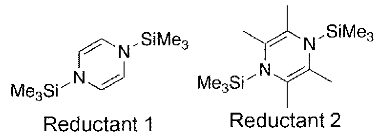
[0147] 前駆体溶液 (1) :還元剤 1を添加したベロブスカイ ト前駆体溶液
グローブボックス内にて 3门12 (1341 1119, 3.611111101), 八1 (4641119, 2.71111110 〇, 11/1八1 (1431119, 0■ 911111101), 3 2 (561119, 0.3611111101) を超脱水 01^0 (4.0 1_) に 45 ° にて溶解させた。 1時間 45 ° にて撹拌後,
 フィルターを用 いて濾過し,

)— 1,4—〇1.||1〇1「〇卩 「32.1门6 (1) (7.91119, 0.035111111〇1)を 01^(50 1_)に 65。 0 にて溶解させ, これを
 1.3 !·滴下した。 還 兀剤'!の添加によって, 黄色の卩八0.7511/1八0.258^3刖駆体溶液は深緑色の懸濁液へと 変化した。 15分間 45 ° にて撹拌すると懸濁液は再び黄色の溶液となり金属

[0148] 前駆体溶液 (2) :還元剤 2を添加したぺロブスカイ ト前駆体溶液
グローブボックス内にて 3门12 (1341 1119, 3.611111101), 八1 (4641119, 2.71111110 〇, 11/1八1 (1431119, 0.911111101), 3 2 (561119, 0.3611111101) を超脱水 01^0 (4.0

035111111〇1)を 01^(50 1_)に 65 ° 0にて溶解させ, これを 1 〇11_のド八0.751^0.253门13 前駆体溶液に 1.3 !·滴下した。 還元剤 2の添加によって, 黄色のド\751^0.253 3前駆体溶液は深緑色の懸濁液へと変化した。 15分間 45 ° にて撹拌すると懸 濁液は再び黄色の溶液となり沈殿が生成した。 ?丁ド£フィルターを用いて濾過 して沈殿を除き, 前駆体溶液
 添加) を得た
。 同様にして, 還元剤 2を Snl2に対して 1.0および 10.0 moL%添加した溶液を得 た。
添加) を得た
。 同様にして, 還元剤 2を Snl2に対して 1.0および 10.0 moL%添加した溶液を得 た。
実施例 2
[0149] 逆 ¾1」構造のスズ系べロブスカイ ト ¾1」太陽電池作製
パターン化した透明導電性ガラス基板 (IT0, 25 mmX25 mm, 5 Q, Geomat ec Co., Ltd. Japan) を, 1 w%中性洗剤水溶液, アセトン, 2 -プロパノール の順でそれぞれ 10分間超音波洗浄した。 最後に, 15分間の UVオゾン洗浄を行 った。
[0150] PEDOTiPSS (Clevious P VP AI 4083) の水分散液を PTFEフィルターにより 濾過した後に, IT0基板上に約 400 ML塗布し, スピンコートした (スロープ 1 秒で 500 rpm にし, 9秒間スピンコートした後に, スロープ 1秒で 4000 rpmに し, 60秒間スピンコートし, スロープ 1秒で停止させた) 。 続いて, 基板を 14 0 ° Cで加熱して約 20 nmの膜厚の PED0T:PSS層 (正孔輸送層)を成膜した。 得ら れた基板をグローブボックスに入れ, 続くベロブスカイ ト層の成膜を行った
[0151] ぺロブスカイ ト前駆体溶液 (1)の調製と同様にして, 還元剤 1を Snl2に対して 0.1, 0.5, 1.0,および 5.0m〇a添加したぺロブスカイ ト前駆体溶液を得た。 これを PED0T:PSS基板上に約 200 ML塗布し, スピンコートし, その最中に 65 ° Cに加温したクロロベンゼンを 300 ML滴下し, 褐色の膜を得た (スロープ 5 秒で 5000 rpm にし, さらに 60秒間スピンコートした最後の 2秒から 1秒の間で クロロベンゼンを滴下し, スロープ 1秒で停止させた) 。 得られた褐色膜を,
45 °Cで 10分間, 65 °Cで 10〜 30分間アニールし, その後 100 °Cで 5分間, 続い て 100 °Cで 30分間アニールして, 黒色のぺロブスカイ ト層を作製した。
得られたベロブスカイ ト膜に, C60 (20 nm), BCP (8 nm), Ag (100 nm)を真 空蒸着にて積層して, 逆型構造のスズ系べロブスカイ ト型太陽電池素子を作 製した。
[0152] ぺロブスカイ ト膜の表面 SEM観察により, 還元剤 1の添加の有無や量の違い ではべロプスカイ ト結晶の形態に変化がなく, いずれの場合も表面被覆率が
\¥0 2020/175705 42 卩(:17 2020 /008529
高く緻密な膜が得られることを確認した (図 5)。 不活性ガス雰囲気下で太陽 電池特性を評価したところ, 還元剤 1を添加したデバイスにおいて, 短絡電流 密度 ( 。 (電圧〇 の際の電流密度」) ) , 開放電圧 (V。。 (電流密度」 = 0の 時の電圧 V) ) が向上し, その光電変換効率 0£) は還元剤 1を 0. 5 1110 1%加え ることで最大の 7. 05%となった (図 6 , 表 1)。
[0153] [表 1 ]

0.0 17.72 0,50 0.46 4.03 5.9 87
0.1 19.00 0.58 0.64 6.97 3.3 302
0.5 18.69 0.58 0.65 7.05 3.2 274
1.0 18.33 0.56 0.61 6.25 3.5 266
5.0 14.47 0,48 0.59 4.06 3.8 215
実施例 3
[0154] 逆 構造のスズ系べロブスカイ ト 太陽電池作製
ベロブスカイ ト前駆体溶液(2)の調製と同様にして, 還元剤
 に対して 0. 5, 1 . 0, 5. 0, および 10. 0 111〇 添加したぺロブスカイ ト前駆体溶液を得た 。 これを用いて実施例 2と同様にして逆型構造のスズ系べロブスカイ ト型太 陽電池素子を作製した。
ベロブスカイ ト膜の表面
 観察により, 還元剤 2の添加の有無や量の違い ではべロブスカイ ト結晶の形態に変化がなく, いずれの場合も表面被覆率が 高く緻密な膜が得られることを確認した (図 7)。 不活性ガス雰囲気下で太陽 電池特性を評価したところ, 還元剤 2の添加によって, 。が向上し,
 は還元剤
は還元剤
 表 2)。 。が増加したのは, ぺロブスカイ ト層内でのキヤリアの再結合が抑え られたためだと考えられる。
[0155] [表 2]

0.0 20.27 0.56 0.72 8.12 2.8 460
0.5 20.71 0.56 0.71 8.25 2.6 668
1.0 20.68 0.56 0.72 8.45 2.5 574
5.0 17.91 0.45 0.68 5.52 2.6 425
10.0 11.62 0.29 0.61 2.04 3.5 390

実施例 4
[0156] 再現#の確認
ベロブスカイ ト前駆体溶液 (2) の調製と同様にして, 還元剤 2を
 に対 して 1 . 0 111〇 添加したベロブスカイ ト前駆体溶液と添加しない溶液を調整し た。 これを用いて実施例 2と同様にして逆型構造のスズ系べロブスカイ ト型 太陽電池素子をそれぞれ 2 0個ずつ作製した。 これらに対し, 不活性ガス雰 囲気下で太陽電池特性を評価した。 その結果, 還元剤 2の添加による 。の増 加が再現性良く確認され, V。。, ドドはほぼ同程度の値を示した (図 9 , 1 0 , 1 1)。 結果として,
 は平均で 6. 9%から 7. 5%にまで向上することが明らか となった (図 1 2)。
実施例 5
[0157] ぺロブスカイ ト層の厚膜化
後述の様にして調整したぺロブスカイ ト前駆体溶液 (3) を用いて実施
\¥02020/175705 44 卩(:17 2020 /008529
例 2と同様にして逆型構造のスズ系べロブスカイ ト型太陽電池素子を作製した ベロブスカイ ト膜の表面
 観察により, 前駆体溶液の濃度を 0.911/1から 1.2 , 1.3, 1.411/1と高くすることでぺロブスカイ ト結晶の粒径が約 500 から約 1 |11まで大きくなっていることが分かった。 また, 還元剤 2の添加の有無では ベロブスカイ ト結晶の形態に変化がなく, いずれの場合も表面被覆率が高く 緻密な膜が得られることを確認した (図 1 3)。
また, 得られた素子の断面 観察を行ったところ, ぺロブスカイ ト層の膜 厚は, 前駆体溶液の濃度を 0.9 11/1から 1.2, 1.3, 1.411/1と高くすることで 210 (0.911/1) から 450 (1.411/1) にまで厚くなっていることが分かった (図 1 4) 得られた素子に対して, 不活性ガス雰囲気下で太陽電池特性を評価したと ころ, いずれの濃度の前駆体溶液(1.2, 1.3, 1.411/1 )を用いた場合において も還元剤 2の添加によって, 。が向上した(図 1 5, 表 3)。 また, 膜厚の増加 に相関して 。が増加し, 還元剤 2を
 に対して 1.0 1110 添加した 1.411/1の前駆 体溶液を用いて作製した素子が本検討において最も高い 8.
 を示した 。 この結果から, キャリア寿命の長寿命化によって, 450 程度の厚膜のぺ ロブスカイ ト層を用いても効率的な電荷の回収が可能であることが明らかに なった。
[0158] [表 3]

1.2 0.0 17.85 0.45 0.44 3.55 6.8 67
1.2 1.0 20.76 0.58 0.66 7.96 2.9 296
1.3 0.0 19.38 0.58 0.67 7.43 3.0 175
1.3 10 2079 057 066 7.84 30 295
1.4 0.0 20.08 0.55 0.64 7.05 3.2 202
1.4 1.0 20.88 0.56 0.69 8.14 2,5 255
〇 2020/175705 45 卩(:171? 2020 /008529
[0159] なお, ぺロブスカイ ト前駆体溶液 (3)は, 以下のようにして得た。
[0160] 前駆体溶液 (3) :還元剤 2を添加したベロブスカイ ト前駆体溶液
グローブボックス内にて 3门12 (1341 1119, 3.6 11111101), 八1 (4641119, 2.7 1111110 〇, 11/1八1 (143 1119, 0.9 11111101), 3 2 (56 1119, 0.36 11111101) を超脱水 01^0 (3.0
 ィルターを用 いて濾過し, ド八0.7 0.2>13前駆体溶液 (1.2 11/1) を調製した。 同様にして, ド八0 .7511/1八0.2>13前駆体溶液 (1.3 11/1および 1.411/1)を調製した。

— 1 , 4— 13.13(
 (2) (9.9 1119, 0■ 035
11100を 01^(50 !·)に 65 ° にて溶解させ, 1 1111_のド八0.751^0.2>13前駆体溶液 (
1.2 11/1) に, これを 17 !·滴下した。 還元剤 2の添加によって, 黄色のド\7 八0. 2>13前駆体溶液は深緑色の懸濁液へと変化した。 15分間 45 ° にて撹拌する と懸濁液は再び黄色の溶液となり沈殿が生成した。
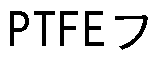 ィルターを用いて 濾過して沈殿を除き, 還元剤 2を 1.0 1110 添加したド八0.751^0.253 3前駆体溶液 (1 .2 11/1)を得た。 同様にして, 還元剤 2を 1.0 (11〇 添加したド八0.751^0.2 13前駆体 溶液 (1.3 11/1および 1.4
 を得た。
を得た。
実施例 6
[0161] 還元剤 2の添加法の最谪化
グローブボックス内にて ( 1 ) 门 (335 1^, 0.9 111111〇〇, ド八1 (116 1^, 0■

9 11/1), (3) 3 2の 1^0溶液 (0.09 11/1), を調整した。
[0162] 2, 3, 5, 6—士61;「311161;11 I— 1 , 4— 13.13(1;「 .111161;11 .1 I)— 1 , 4—〇1.111 〇1「〇卩 「32.1门
0 (2) (9.9 1^. 0.035 11111100を 01^(50 !·)に 65 ° にて溶解させ, これを 1
〇 2020/175705 46 卩(:171? 2020 /008529
1111の溶液 (2) , (3) , (4) にそれぞれ 13 !·滴下した。 (2) にド八1 (
116 1119, 0.7 11111101) , 11/1八1 (36 1119, 0■ 2 11111101), 3 2 (141119, 0.09 111111〇1)を, (3) に 3门12 (335 1119, 0■ 9 11111101), 八1 (116 1119, 0.7 11111101), 11/1八1 (36 1119, 0 .2 11111101)を加えド八0.751^0.2 13前駆体溶液 (0.9 11/1) を調整した。 これらの溶液 (1 ) 〜 (4) を用いて実施例 1 と同様にして石英基板上にぺロブスカイ ト 層を成膜した。
[0163] 得られたぺロブスカイ ト膜の表面
 により,
により,

を加えた場合
 (2) ) のみ, ぺロブスカイ ト結晶の粒径が約 2 111ま で大きくなっていることが分かった (図 1 6— 2)。

ルが 0.02 6 程度短波長へシフトし, 半値全幅が 104
 くなっているこ とがわかった (図 1 7)。 短波長へシフトした理由は, ぺロブスカイ ト結晶の 粒径が大きくなったことで, 再結合サイ トとなりやすい結晶の表面積の割合 が減ったためと推察される。 また, 発光寿命は
 + および (4) ) に, そ
 (2) の結果について はべロブスカイ ト結晶の粒径増大の寄与が大きいと考えられる (図 1 8)。
[0165] そこで, これらの前駆体溶液 ( 1 ) , (2) , (4) を用いて, 実施例 2 と同様にして [ 〇丁 基板上にベロブスカイ ト層を成膜した。 得られたベロ ブスカイ ト膜の表面 観察により, いずれの方法で調製した前駆体溶液を用 いた場合にも 1 111以下の粒径のぺロブスカイ ト結晶が形成されていることが 分かった (図 1 9)。 これらの膜を用いて実施例 2と同様にして作製した逆型 構造デバイスに対して, 太陽電池特性を評価したところ, ド八1 + 1^1 + 3^2 十
 (8.0 %) が得られた (図 20, 表 4)。
[0166]
[表 4]
Entry

1 12.14 0.49 0.59 3.48 6.3 132
2 17.22 0.51 0.56 4.95 3.8 218
4 20,23 0.56 0.70 8.03 2.5 263 実施例 7
[0167] 混合系べロブスカイ ト膜の光物#測定
後述の様にして調整した, 8 _を 0.0〜 25%まで加えた I— 8「混合系べロブス カイ ト前駆体溶液 (4) を用いて実施例 1 と同様にして石英基板上にぺロブ スカイ ト層を成膜し I測定および時間分解 I測定を行った。
い測定および時間分解 い測定より, いずれの
 混合系べロブスカイ ト膜 も還元剤 2の添加によって, 蛍光波長を保持しながら蛍光寿命が顕著に長くな り, 2 程度から最大で 11 まで長くなることが確認できた (図 21 , 22 )。 これは, ド\751^0.2 13の場合と同様に, ぺロブスカイ トの構造や組成は保 持しながら, 光励起によって生成したキヤリアの再結合が抑えられたことを 示唆している。
[0168] なお, ぺロブスカイ ト前駆体溶液 (4)は, 以下のようにして得た。
[0169] 前駆体溶液 (4) : 1_日「混合系べロブスカイ ト前駆体溶液
グローブボックス内にて 3门12 (3351119, 0■ 911111101), (841119, 0■ 7 11111101 ) , 1^1 (361119, 0■ 211111101), 3 2 (141119, 0.0911111101) を超脱水 01^0 (1.0 〇11_ ) に 45 ° にて溶解させた。 45 ° にて 1時間撹拌後,
 フイルターを用い て濾過し,
 同 様にして 8「をそれぞれ 5%および 10%混合したド八0.75MA0.25Snd0.95B「0.05) 3およびド八0 .7 0.2>(10.8 0.10)3前駆体溶液を調製した。 また, 2, 3, 5, 6-士61;「311161;11 ー1 , 4— 13.13(
 (2) (9.91119, 0.035111111
)を 01^(50 !·)に 65 ° にて溶解させ, これを 500 しのド八0.751^0.2 (11_ )()
3(x=0.0, 0.05, 0.10, 0.25) 前駆体溶液に 6.5 ML滴下した。 還元剤 2の添加 によって, 黄色の FAusMAwsSndnBrJs(x=0.0, 0.05, 0.10, 0.25) 前駆体溶 液は深緑色の懸濁液へと変化した。 15分間 45° Cにて撹拌すると懸濁液は再び 黄色の溶液となり沈殿が生成した。 PTFEフィルターを用いて濾過して沈殿を 除き, 還元剤 2を Snl2 (換算) に対して 1.0m〇a添加した FVJAuSndmBrA (x=0.0, 0.05, 0.10, 0.25) 前駆体溶液を得た。
実施例 8
[0170] 順 ¾1」構诰のスズ系べロブスカイ ト ¾1」太陽雷池
パターン化した透明導電性ガラス基板 (FT0, 25 mm X 25 mm, Asahi Glass Co., Ltd., Japan) を, 1w%中性洗剤水溶液, アセトン, 2 -プロパノール及 び蒸留水の順でそれぞれ 10分間超音波洗浄した。 最後に, 15分間の UVオゾン 洗浄を行った。
エタノール (wako, 超脱水) 39 mLにチタンジ (イソプロポキシド) ビス ( アセチルアセトナート) (Ti(0iPr)2(acac)2, 2—プロパノールの 75質量%溶液 , Tokyo Chemical Industry Co. , Ltd. , Japan) を 1 mL加えた。 上記の FTO基 板 (透明電極) を 450 °Cのホッ トプレート上に並べ, Ti(0iPr)2(acac)2溶液を スプレー (キャリアガス: N2, 0.5 MPa) で吹き付け, コンパクト Ti02層 (約 3 0 nm) を作製した。 さらに, 得られた基板を, T i C 14 (440 /,l, special grad e, Wako Pure Chemical Industries Ltd. , Japan) の水溶液 100 mLに 70 °Cで 30分間浸潰した。 その後, 基板を 500 °Cで 20分間焼成し, (正孔) ブロッキ ング層を形成した。
[0171] 得られたコンパクト ^(^層 ( (正孔) ブロッキング層) の上に, Ti02ぺース 卜 (PST— 18NR, JGC Catalysts and Chemicals Ltd.) のエタノール溶液 (pa ste: ethano 1= 1 : 8(質量比)) を約 190 ML滴下してスピンコートすることで , 約 100〜 150 nmの厚みのメソポーラス Ti02層 (電子輸送層) を形成した。
[0172] 直前に UVオゾン処理したメソポーラス Ti02層 (電子輸送層) まで作製した基 板をグローブボックスに入れた。 ベロブスカイ ト前駆体溶液(4)を PED0T:PSS 基板上に約 200 ML塗布し, スピンコートし, その最中に 65 ° Cに加温したク
\¥0 2020/175705 49 卩(:17 2020 /008529
ロロベンゼンを 300 し落とし, 褐色の膜を得た (スロープ 5秒で 5000 111 に し, さらに 60秒間スピンコートした最後の 2秒から 1秒の間でクロロベンゼン を滴下し, スロープ 1秒で停止させた) 。 得られた褐色膜を, 45 °〇で 10分間 , 65 °〇で 10〜 30分間アニールし, その後 100 °〇で 5分間, 続いて 100 °〇で 30 分間アニールして, 黒色のぺロブスカイ ト層を作製した。
[0173] 正孔輸送材料 (卩丁八八;ポリ [ビス(4 -フエニル)(2, 4, 6 -トリメチルフエニ ル)アミン], 20. 2 1119) と 4—イソプロピルー 4' —メチルジフエニルヨードニ ウムテトラキス(ペンタフルオロフエニル)ボレート
 2. 7 11^)を 1 111の クロロベンゼンに溶解させた。 30分間撹拌後, 溶液をメンブランフィルター でろ過し, ろ液をぺロブスカイ ト層上にスピンコートした。 得られた基板を 7 0 °〇で 5分間アニールして正孔輸送層を成膜した後, 真空蒸着により, 正孔輸 送層の上に 80 の金電極を積層して, 順型構造のスズ系べロブスカイ ト型太 陽電池を得た。
[0174] 不活性ガス雰囲気下で太陽電池特性を評価したところ, 還元剤 2の添加によ って, 。が向上し, その
 は還元剤 2を
 (換算) に対して 1 . 0 111〇 添加し たド八0.75^八0.25 ( #「ø.05) 3刖駆体溶液を用いて作製した素子において, 本検目寸 において最大の 2. 9%となった (図 2 3 , 表 5)。 また, 各素子の外部量子収率 (^)を測定したところ, 還元剤 2を (換算) に対して 1 . 0 111〇 添加した 八

80%を超える高い値を示した (図 2 4)。
[0175] [表 5]


れたことから, 還元剤 2の
 への反応性は高くないことが分かった (図 2 5) 。 一方で, (2) に関して, 還元剤 2の添加後には
 由来のピークが無くな ったことから, 溶液中の 2価のスズが還元され, 固体の 0価のスズとして析出 したと考えられ, このことは還元剤 2の
 への反応性が高いことを示唆して いる (図 2 6)。
[0178] この現象に関して,
 に対して還元剤 2を加えて得 られる懸濁液に対して透過型電子顕微鏡による観察を行ったところ, 粒径が 1 5 程度までのナノ粒子が形成されていることを確認した (図 2 7)。
[0179] 続いて, (3) に関して, 還元剤 2の添加後では
 に由来するピークに加 えて, わずかに
 に由来するピークが得られ, 還元剤 2によ
 が部分的 に還元されていることが確認された (図 2 8)。 (4) に関して,
 の存在 下で還元剤 2を添加した後では, 4価のスズに由来するピークが完全になく なり,
 に由来するピークのみが得られた (図 2 9)。 この結果は,
 還元によって生成した反応活性の高い 0価の Snナノ粒子と
 を係中で反応さ せることで, 4価のスズが効果的に還元されたということを示唆している。 実施例 10
[0180] の添加による光物#. 太陽電池特忡への効果
後述の様にして調整した, [士 を に対して 0. 0~ 10. 0 1110 まで加えた ベロブスカイ ト前駆体溶液 (5)を用いて実施例 1 と同様にして石英基板上に
〇 2020/175705 51 卩(:171? 2020 /008529
ベロブスカイ ト層を成膜し, 時間分解 測定を行った。

[0181] 続いて, ぺロブスカイ ト前駆体溶液 (5) を用いて, 実施例 2と同様にして 逆型構造のスズ系べロブスカイ ト型太陽電池素子を作製した。 得られたベロ ブスカイ ト膜の表面 画像より, [ の添加の有無やその量はベロブスカ イ ト結晶形態に影響しないことが分かった (図 3 1) 。 不活性ガス雰囲気下 で太陽電池特性を評価したところ, 時間分解 い測定の結果から予想されるよ うに,
 に対して
に対して
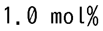 加えた場合に
 となった (図 32) 。 この結果は, やはり ぺロブスカイ ト層内で生成したキヤリアの再結合が抑制されたことを示唆し ている。
[0182] 前駆体溶液(5) : _1 Hを添加したぺロブスカイ ト前駆体溶液
グローブボックス内にて 3门12 (1341 1119, 3.6 11111101), 八1 (4641119, 2.7 1111110 〇, 11/1八1 (143 1119, 0.9 11111101), 3 2 (56 1119, 0.36 11111101) を超脱水 01^0 (4.0
 ィルターを 用いて濾過し, ド八0.7 0.2 13前駆体溶液を調製した。 脱気脱水した巳 を 1 111!_のド八0.751^0.253 3前駆体溶液に 1.4 !~滴下した。 15分間 45 ° にて撹拌した 後に, 卩丁ド巳フィルターを用いて濾過し, 前駆体溶液
 に対して 1.0
 £ 士 添加) を得た。 同様にして, [士 を
 に対して 5.0および 10.0 1110 添加した溶液を得た。
実施例 11
[0183] 八サイ トカチオンの提供
ぺロブスカイ ト層の作成過程で欠陥を生じていると仮定し, ぺロブスカイ 卜前駆体溶液に サイ トカチオン源を混合することとした。
[0184]
 を用いて〇. 91\/1のド八3 3前駆体溶液 を調整した。 クロロベンゼンを貧溶媒として用い, プラズマ洗浄後の液晶基
\¥02020/175705 52 卩(:17 2020 /008529
を用いて〇. 91\/1のド八3 3前駆体溶液 を調整した。 クロロベンゼンを貧溶媒として用い, プラズマ洗浄後の液晶基
\¥02020/175705 52 卩(:17 2020 /008529
板に 5000 「 にて 60秒間スピン塗布し, 他の条件は実施例 1 と同様 にして, ぺロブスカイ ト層を作成した。
この際, 前駆体溶液に 5質量%の 巳八 I を添加したものと, しないもの
»
1質量%の TM_DH P (還元剤 2) を添加したものと, しないもの, クロロベンゼンが室温のもの (1^〇 1~1八丁) と, クロロベンゼンが 65°〇 のもの (1~1八丁法)
を用いた。
[0185] 得られたぺロブスカイ ト層について, 時間分解 !_測定を行った。 その結 果を図 33に示す。 図 33は, 八サイ ト源の影響を分析するための時間分解 !_測定結果を示す図面に代わるグラフである。 グラフの最も上部に位置す るものは, 前駆体溶液に 5質量%の P EA \ , 及び 1質量%の丁 IV! _ 01~1 (還元剤 2) を添加し, クロロベンゼンが 65°〇のものである。 次が, 前駆 体溶液に 5質量%の 巳 丨 を添加し, TM_DH P (還元剤 2) を添加せ ず, クロロベンゼンが 65°〇のものである。 各ぺロブスカイ トの蛍光寿命を 表 6に示す。
[0186] [表 6]

[0187] 表 6から, 八サイ トカチオン源を前駆体溶液に添加することで, 虽光寿命
〇 2020/175705 53 卩(:171? 2020 /008529
が向上することが分かる。 また, 表 6から 1~1八丁法を用いることによっても 虽光寿命が向上することが分かる。 さらに, 表 6から還元剤が存在している 条件で、 サイ トカチオン源を前駆体溶液に添加し, 1~1 丁法を用いること により蛍光寿命が飛躍的に向上することが示された。
[0188] この実施例では, 八サイ トカチオン源として, P E A (ヨウ化フエニル エチルアミン: 〇2 1~1 4 1\1 1~1 3 丨) を用いた。 この例では, 八サイ トカチオ ン源は, アミン系カチオン (フエニルエチルアミンイオン: 〇2 1~1 4 1\1 1~1 3 +) である。 例えば, フエニルエチルアミンイオンは, 芳香族アミン系陽イオ ンであり, 芳香族アミン系陽イオンはアンモニウムイオンと芳香族分子部分 とが存在するため, フエニルエチルアミンイオンと同様に機能すると考えら れる。 八サイ トカチオン源は, その機能から前駆体溶液に〇. 5質量%以上 2 0質量%以下存在すればよく, 1質量%以上 1 0質量%以下でもよいと考 えられる。
[0189] この実施例では, 貧溶媒として 6 5 °〇のクロロベンゼンを用いた (1~1八丁 法) 。 貧溶媒は 4 0 °〇以上 8 0 °〇以下であっても同様に機能すると考えられ る。
産業上の利用可能性
[0190] 本発明は, ぺロブスカイ ト層の製造方法などに関するため, 太陽電池や有 機巳 !_素子を製造するための産業において利用されうる。
Claims
[化 1 ]

(式 (丨) 中,
 は, 同一でも異なってもよく, 水素原子, 又は <3 1〜<3 4アルキル基を示し,

X !及び乂2は, 同一でも異なってもよく, !\1又は炭素原子を示す
\¥0 2020/175705 55 卩(:171? 2020 /008529

[化 2]

(式 (丨 丨) 中,
 同一でも異なってもよく, 水素原 子, 又は〇1〜〇4アルキル基を示し,

乂3及び乂4は, 同一でも異なってもよく, 1\1又は炭素原子を示す

[化 3]

(式 (丨 丨 丨) 中,
 同一でも異なってもよく, 水素 原子, 〇1 ~〇4アルキル基, 〇2 ~〇4アルケニル基, 〇2 ~〇4アル キニル基, 〇1〜〇4アルコキシ基, 〇1〜〇4アルキルチオ基, アリ —ル基, アリールオキシ基, 又はアリールチオ基を示す。 )
\¥02020/175705 56 卩(:171? 2020 /008529
同一でも異なってもよく, 水素 原子, 〇1 ~〇4アルキル基, 〇2 ~〇4アルケニル基, 〇2 ~〇4アル キニル基, 〇1〜〇4アルコキシ基, 〇1〜〇4アルキルチオ基, アリ —ル基, アリールオキシ基, 又はアリールチオ基を示す。 )
\¥02020/175705 56 卩(:171? 2020 /008529
[化 4]
#5
乂5— 8|一 6
( I V )
(式 (丨 V) 中,
 同一でも異なってもよく, 水素原 子, 〇1~〇4アルキル基, 〇2~〇4アルケニル基, 〇2~〇 4アルキ ニル基, 〇1〜〇4アルコキシ基, 〇 1〜〇4アルキルチオ基, ァリ_ ル基, アリールオキシ基, 又はアリールチオ基を示し, 乂5は, ハロゲン原子を示す。 )
[化 5]

(式 (V) 中,
 同一でも異なってもよく, 水素原子 , 〇1~〇4アルキル基, 〇2~〇4アルケニル基, 〇2~〇4アルキニ ル基, 〇1〜〇4アルコキシ基, 〇 1〜〇4アルキルチオ基, アリール 基, アリールオキシ基, 又はアリールチオ基を示す。 ) 。
[請求項 4] 請求項 1 に記載の方法であって, 前記還元剤の酸化還元電位は, サ イクリックボルタンメ トリーで酸化電位が一 1.0 V ド〇 〇+以上 +0. 8 V ド〇/^〇+以下である, 方法。
[請求項 5] 請求項 1 に記載の方法であって,
前記重ハロゲン化スズは, S n Xml (Xは I , 巳 「, 〇 丨のい ずれか 1種以上であり, 011は, ·! . 8£〇11 £ 2. 2) で示される , 方法。
\¥0 2020/175705 57 卩(:171? 2020 /008529
[請求項 6] 請求項 1 に記載の方法であって,
前記重ハロゲン化スズは, ヨウ化スズを含む, 方法。
[請求項· 7] 請求項 6に記載の方法であって,
前記重ハロゲン化スズは, さらに臭化スズおよび塩化スズのいずれ か 1種以上を含む, 方法。
[請求項 8] 請求項 1 に記載の方法であって,
前記スズ系べロブスカイ ト前駆体溶液中の還元剤の濃度は, 前記ス ズ系ぺロブスカイ ト前駆体溶液中に添加するフッ化スズの濃度よりも 小さい, 方法。
[請求項 9] 請求項 1 に記載の方法であって,
前記スズ系べロブスカイ ト前駆体溶液は, さらに芳香族アミン系陽 イオンを含む, 方法。
[請求項 10] 請求項 1 に記載の方法であって,
前記スズ系べロブスカイ ト前駆体溶液を基板に塗布する工程と, 前記スズ系ぺロブスカイ ト前駆体溶液を前記基板に塗布した後に, 貧溶媒を前記基板に塗布する工程を含み,
前記貧溶媒を含む溶液は, 4 0 °〇以上 8 0 °〇以下である, 方法。
[請求項 1 1 ] 不純物を含む重ハロゲン化スズの溶液に, 還元剤を添加する還元剤 添加工程であって,
前記重ハロゲン化スズの溶液は, ヨウ化スズ, 臭化スズおよび塩化ス ズから選ばれる 1種又は 2種以上を含み,
前記不純物は, フッ化スズを含み,
前記還元剤は, フッ化スズをスズに還元し, 前記重ハロゲン化スズを スズに還元しない還元剤である工程と,
前記還元剤添加工程の後に, 前記重ハロゲン化スズ由来の物質を取 得する取得工程とを含む,
重ハロゲン化スズ系物質の精製方法。
[請求項 12] 不純物を含む重ハロゲン化スズの溶液に, 還元剤を添加する還元剤
〇 2020/175705 58 卩(:171? 2020 /008529
添加工程であって,
前記重ハロゲン化スズの溶液は, ヨウ化スズ, 臭化スズおよび塩化ス ズから選ばれる 1種又は 2種以上を含み,
前記不純物は, 4価のスズイオンを含み,
前記還元剤は, フッ化スズをスズに還元し, 前記重ハロゲン化スズを スズに還元しない還元剤である工程と,
前記還元剤添加工程の後に, 前記重ハロゲン化スズ由来の物質を取 得する取得工程とを含む,
重ハロゲン化スズ系物質の精製方法。
[請求項 13] 請求項 1 1 または 1 2に記載の方法であって,
前記還元剤添加工程の後に, 沈殿物を除去する沈殿物除去工程と, 前記沈殿物除去工程の後に, 前記沈殿物を除去した溶液を静置する 静置工程をさらに含み,
前記取得工程は, 前記静置工程により析出した結晶を得る結晶取得 工程を含む, 方法。
[請求項 14] 重ハロゲン化スズと, フッ化スズと, 還元剤とを含む溶液であって 前記重ハロゲン化スズは, ヨウ化スズ, 臭化スズおよび塩化スズか ら選ばれる 1種又は 2種以上を含み,
前記還元剤は, 前記溶液中のフッ化スズをスズに還元し, 前記溶液 中の前記重ハロゲン化スズをスズに還元しない還元剤である, 溶液。
[請求項 15] 請求項 1 4に記載の溶液であって, 前記溶液は, スズ系べロプスカ イ ト前駆体溶液である, 溶液。
[請求項 16] スズ系ぺロブスカイ ト層であって,
前記スズ系べロブスカイ ト層は, 0価のスズ, ピラジン系化合物, ケイ素系化合物, 及びゲルマニウム系化合物から選ばれる 1種又は 2 種以上を合計で〇. 0 1 111以上 1 0 0 0 以下含む, スズ系 ぺロブスカイ ト層。
〇 2020/175705 59 卩(:171? 2020 /008529
[請求項 17] 発光性材料であって,
前記発光性材料は, 0価のスズ, ピラジン系化合物, ケイ素系化合 物, 及びゲルマニウム系化合物から選ばれる 1種又は 2種以上を合計 で 0 . 0 1 01以上 1 0 0 0 以下含む, スズ系ぺロブスカイ 卜を含む, 発光性材料。
[請求項 18] スズ系ぺロブスカイ ト層を有する光電変換素子であって,
前記スズ系べロブスカイ ト層は, 0価のスズ, ピラジン系化合物, ケイ素系化合物, 及びゲルマニウム系化合物から選ばれる 1種又は 2 種以上を合計で〇. 0 1 111以上 1 0 0 0 01以下含む, 光電変 換素子。
Priority Applications (1)
| Application Number | Priority Date | Filing Date | Title |
|---|---|---|---|
| JP2021502668A JP7432088B2 (ja) | 2019-02-28 | 2020-02-28 | スズ系ペロブスカイト層の製造方法,重ハロゲン化スズ系物質の精製方法,溶液,スズ系ペロブスカイト層,発光性材料,及び光電変換素子 |
Applications Claiming Priority (2)
| Application Number | Priority Date | Filing Date | Title |
|---|---|---|---|
| JP2019036863 | 2019-02-28 | ||
| JP2019-036863 | 2019-02-28 |
Publications (1)
| Publication Number | Publication Date |
|---|---|
| WO2020175705A1 true WO2020175705A1 (ja) | 2020-09-03 |
Family
ID=72239815
Family Applications (1)
| Application Number | Title | Priority Date | Filing Date |
|---|---|---|---|
| PCT/JP2020/008529 Ceased WO2020175705A1 (ja) | 2019-02-28 | 2020-02-28 | スズ系ペロブスカイト層の製造方法,重ハロゲン化スズ系物質の精製方法,溶液,スズ系ペロブスカイト層,発光性材料,及び光電変換素子 |
Country Status (2)
| Country | Link |
|---|---|
| JP (1) | JP7432088B2 (ja) |
| WO (1) | WO2020175705A1 (ja) |
Cited By (4)
| Publication number | Priority date | Publication date | Assignee | Title |
|---|---|---|---|---|
| JPWO2022244289A1 (ja) * | 2021-05-19 | 2022-11-24 | ||
| CN116018039A (zh) * | 2022-12-26 | 2023-04-25 | 南方科技大学 | 一类锡基钙钛矿材料及其制备方法与应用 |
| WO2023068015A1 (ja) | 2021-10-18 | 2023-04-27 | Ckd株式会社 | 錫系ペロブスカイト層の製造方法 |
| CN117106438A (zh) * | 2023-07-07 | 2023-11-24 | 北京大学 | 一种核壳结构锡基钙钛矿纳米晶制备方法及应用 |
Families Citing this family (3)
| Publication number | Priority date | Publication date | Assignee | Title |
|---|---|---|---|---|
| CN114388698B (zh) * | 2022-01-05 | 2025-03-14 | 大连理工大学 | 一种预质子化氨基吡啶辅助制备高效钙钛矿太阳能电池的方法 |
| CN115666196B (zh) * | 2022-11-01 | 2026-03-27 | 仁烁光能(苏州)有限公司 | 一种锡铅混合钙钛矿供液系统及其使用方法 |
| CN120614936A (zh) * | 2024-03-08 | 2025-09-09 | 宁德时代新能源科技股份有限公司 | 太阳能电池及其制备方法、用电设备、发电设备 |
Citations (1)
| Publication number | Priority date | Publication date | Assignee | Title |
|---|---|---|---|---|
| JP2016528384A (ja) * | 2013-06-28 | 2016-09-15 | ウェイン ステイト ユニバーシティー | 基板上に層を形成するための還元剤としてのビス(トリメチルシリル)6員環系および類縁化合物 |
-
2020
- 2020-02-28 WO PCT/JP2020/008529 patent/WO2020175705A1/ja not_active Ceased
- 2020-02-28 JP JP2021502668A patent/JP7432088B2/ja active Active
Patent Citations (1)
| Publication number | Priority date | Publication date | Assignee | Title |
|---|---|---|---|---|
| JP2016528384A (ja) * | 2013-06-28 | 2016-09-15 | ウェイン ステイト ユニバーシティー | 基板上に層を形成するための還元剤としてのビス(トリメチルシリル)6員環系および類縁化合物 |
Non-Patent Citations (3)
| Title |
|---|
| OZAKI, MASASHI ET AL., ACS OMEGA, vol. 2, 2017, pages 7 016 - 7021 * |
| STEVENS, ERIC C. ET AL., JOURNAL OF VACUUM SCIENCE & TECHNOLOGY A: VACUUM, SURFACES, AND FILMS, vol. 36, no. 6, 2018 * |
| ZHAO, ZIRAN ET AL., ADVANCED SCIENCE, vol. 4, no. 1-7, 2017 * |
Cited By (7)
| Publication number | Priority date | Publication date | Assignee | Title |
|---|---|---|---|---|
| JPWO2022244289A1 (ja) * | 2021-05-19 | 2022-11-24 | ||
| WO2022244289A1 (ja) * | 2021-05-19 | 2022-11-24 | パナソニックIpマネジメント株式会社 | 半導体材料および光電変換素子 |
| US12660405B2 (en) | 2021-05-19 | 2026-06-16 | Panasonic Intellectual Property Management Co., Ltd. | Semiconductor material and photoelectric conversion element |
| WO2023068015A1 (ja) | 2021-10-18 | 2023-04-27 | Ckd株式会社 | 錫系ペロブスカイト層の製造方法 |
| KR20240069740A (ko) | 2021-10-18 | 2024-05-20 | 시케이디 가부시키가이샤 | 주석계 페로브스카이트층의 제조 방법 |
| CN116018039A (zh) * | 2022-12-26 | 2023-04-25 | 南方科技大学 | 一类锡基钙钛矿材料及其制备方法与应用 |
| CN117106438A (zh) * | 2023-07-07 | 2023-11-24 | 北京大学 | 一种核壳结构锡基钙钛矿纳米晶制备方法及应用 |
Also Published As
| Publication number | Publication date |
|---|---|
| JP7432088B2 (ja) | 2024-02-16 |
| JPWO2020175705A1 (ja) | 2020-09-03 |
Similar Documents
| Publication | Publication Date | Title |
|---|---|---|
| Li et al. | NiO x/spiro hole transport bilayers for stable perovskite solar cells with efficiency exceeding 21% | |
| JP7389018B2 (ja) | Sn系ペロブスカイト層及び太陽電池の製造方法 | |
| JP7432088B2 (ja) | スズ系ペロブスカイト層の製造方法,重ハロゲン化スズ系物質の精製方法,溶液,スズ系ペロブスカイト層,発光性材料,及び光電変換素子 | |
| US10937972B2 (en) | Complex and perovskite material, and perovskite-type solar cell using complex or perovskite material | |
| US11355720B2 (en) | High efficiency large area perovskite solar cells and process for producing the same | |
| Cho et al. | Acridine-based novel hole transporting material for high efficiency perovskite solar cells | |
| Thambidurai et al. | Improved photovoltaic performance of triple-cation mixed-halide perovskite solar cells with binary trivalent metals incorporated into the titanium dioxide electron transport layer | |
| US20160155974A1 (en) | Complex pnictide metal halides for optoelectronic applications | |
| EP3499597A1 (en) | Electron specific oxide double layer contacts for highly efficient and uv stable perovskite device | |
| JP7623714B2 (ja) | 高純度化スズ含有ペロブスカイト半導体材料 | |
| KR20190141742A (ko) | 장기 고 가동 안정성을 갖는 무기 홀 도체 기초 퍼로브스카이트 광전 전환 장치 | |
| US11066431B2 (en) | Complex and method for producing same | |
| EP3518301A1 (en) | Crystal defects mitigating agents for high power conversion efficiency and stability of perovskite photovoltaic devices | |
| EP2804232A1 (en) | High performance perovskite-sensitized mesoscopic solar cells | |
| EP3223323A1 (en) | High efficiency large area perovskite solar cells and process for producing the same | |
| Sakthivel et al. | Efficient and stable planar perovskite solar cells using co-doped tin oxide as the electron transport layer | |
| Xie et al. | High-performance perovskite photodetectors with suppressed dark current density via small molecule in antisolvent strategy | |
| Rahman et al. | Boosting the efficiency of perovskite solar cells through molecular interface-driven grain and defect control | |
| KR101351303B1 (ko) | 고 전도도 정공전달물질 및 이를 이용한 염료감응 태양전지 | |
| JP5347329B2 (ja) | 光電変換素子及び太陽電池 | |
| US20240065093A1 (en) | Compound, and electronic device and light-emitting device using the same | |
| JP2009187821A (ja) | 光電変換素子及び太陽電池 | |
| WO2023054073A1 (ja) | 光電変換素子およびその製造方法、ならびに組成物 | |
| EP4496449A1 (en) | Photoelectric conversion material and photoelectric conversion element using same | |
| Webb | Organometallocenes for high performance perovskite solar cells |
Legal Events
| Date | Code | Title | Description |
|---|---|---|---|
| 121 | Ep: the epo has been informed by wipo that ep was designated in this application |
Ref document number: 20763426 Country of ref document: EP Kind code of ref document: A1 |
|
| ENP | Entry into the national phase |
Ref document number: 2021502668 Country of ref document: JP Kind code of ref document: A |
|
| NENP | Non-entry into the national phase |
Ref country code: DE |
|
| 122 | Ep: pct application non-entry in european phase |
Ref document number: 20763426 Country of ref document: EP Kind code of ref document: A1 |