WO2020170795A1 - フォトニック結晶光共振器 - Google Patents
フォトニック結晶光共振器 Download PDFInfo
- Publication number
- WO2020170795A1 WO2020170795A1 PCT/JP2020/004040 JP2020004040W WO2020170795A1 WO 2020170795 A1 WO2020170795 A1 WO 2020170795A1 JP 2020004040 W JP2020004040 W JP 2020004040W WO 2020170795 A1 WO2020170795 A1 WO 2020170795A1
- Authority
- WO
- WIPO (PCT)
- Prior art keywords
- photonic crystal
- lattice
- lattice element
- optical resonator
- shift
- Prior art date
- Legal status (The legal status is an assumption and is not a legal conclusion. Google has not performed a legal analysis and makes no representation as to the accuracy of the status listed.)
- Ceased
Links
Images
Classifications
-
- G—PHYSICS
- G02—OPTICS
- G02B—OPTICAL ELEMENTS, SYSTEMS OR APPARATUS
- G02B6/00—Light guides; Structural details of arrangements comprising light guides and other optical elements, e.g. couplings
- G02B6/10—Light guides; Structural details of arrangements comprising light guides and other optical elements, e.g. couplings of the optical waveguide type
- G02B6/12—Light guides; Structural details of arrangements comprising light guides and other optical elements, e.g. couplings of the optical waveguide type of the integrated circuit kind
- G02B6/122—Basic optical elements, e.g. light-guiding paths
- G02B6/1225—Basic optical elements, e.g. light-guiding paths comprising photonic band-gap structures or photonic lattices
-
- G—PHYSICS
- G02—OPTICS
- G02B—OPTICAL ELEMENTS, SYSTEMS OR APPARATUS
- G02B6/00—Light guides; Structural details of arrangements comprising light guides and other optical elements, e.g. couplings
- G02B6/10—Light guides; Structural details of arrangements comprising light guides and other optical elements, e.g. couplings of the optical waveguide type
- G02B6/12—Light guides; Structural details of arrangements comprising light guides and other optical elements, e.g. couplings of the optical waveguide type of the integrated circuit kind
- G02B6/13—Integrated optical circuits characterised by the manufacturing method
Definitions
- the present invention relates to a photonic crystal optical resonator.
- Photonic crystals are artificial materials that have a periodic crystal structure consisting of two or more types of media with different refractive indices, and have functions such as light propagation, refraction, reflection control, and light trapping.
- a photonic crystal with a submicron crystal period drastically reduces the size of an optical integrated circuit that uses conventional optical waveguides for light of various wavelengths, or the size of an optical device that is extremely compact and reduces energy consumption. It is especially expected that a significant reduction will be achieved.
- the photonic crystal can be composed of a periodic crystal structure with a lattice element including a base portion and through holes formed in the base portion.
- a photonic crystal two-dimensional photonic crystal
- a resonator can be formed by an optical confinement structure due to a defect obtained by removing lattice elements from lattice points.
- the position of the grid point from which the grid element is removed is called a point defect.
- a resonator having an optical confinement structure composed of one point defect has a 6-fold crystal symmetry in a plan view with respect to the optical confinement structure, and is called an H1 resonator.
- the H1 resonator is one of the smallest photonic crystal optical resonators in terms of actual resonator size (footprint) and optical volume (mode volume: V). However, there is no report up to now on a design in which the mode volume V of the H1 resonator is less than 1( ⁇ /2n) 3 when the slot structure described later is not arranged.
- the slot structure is a structure in which, for example, a rectangular parallelepiped embedded structure called a slot is embedded in the base of the optical confinement structure.
- the width of the slot in the slot structure is generally less than 200 nm, and has the effect of strongly confining the electric field of light in the slot having a small sub-wavelength and strongly enhancing the strength.
- Such properties of the slot structure are considered to be extremely useful for application in capturing atoms and molecules, detecting and capturing molecules and DNA in a biosensor, and realizing a high-performance optical device by filling an active medium.
- a slot having a short length and a very narrow width that fits within a point defect of an H1 resonator is arranged in a portion of an optical confinement structure.
- the mode volume V of the H1 resonator it is possible to design the mode volume V of the H1 resonator to be significantly smaller than 1( ⁇ /2n) 3 while maintaining the single point defect resonator.
- an optical resonator having a Q value of 200,000 and a Q/V of 10 million has been experimentally obtained by the technique described above (see Non-Patent Document 1).
- Patent Document 1 discloses a technique of shifting a plurality of grid elements on the extension line in the longitudinal direction of the slot outward in order to enhance the Q value to a practically useful value.
- the mode volume V of the H1 resonator in the case of a silicon oxide film (refractive index 1.45) is slightly large, about 0.1 ( ⁇ /n) 3 .
- Patent Document 1 since a specific lattice element is shifted for the purpose of enhancing the Q value, the fact that the mode volume V of the H1 resonator becomes large is not taken into consideration.
- the present invention has been made to solve the above problems, and even when the refractive index of the low refractive index medium of the photonic crystal is larger than that of air, the mode volume of the resonator is smaller.
- the purpose is to be able to.
- the photonic crystal optical resonator according to the present invention includes a base and a plurality of columnar lattice elements having a refractive index different from that of the base, and the plurality of lattice elements are arranged on the base at intervals equal to or less than the wavelength of the target light.
- a plate-shaped photonic crystal body that is periodically provided in a lattice shape, an optical confinement portion due to a defect composed of a portion of the photonic crystal body that has no lattice element at the lattice point, and a photonic crystal formed by the lattice element A longitudinal direction extending in the first direction along the ⁇ -K crystal orientation of the optical confinement section, embedded in the base section of the optical confinement section, and having a lower refractive index than the base section.
- One of the modes is said to have only one electric field antinode inside the buried structure, which has a refractive index greater than that of air and is the first on the plane where the grating elements are arranged.
- the first lattice element adjacent to the light confinement portion in the second direction perpendicular to the one direction shifts from the lattice point to the side away from the light confinement portion in the second direction, and is adjacent to the first lattice element in the first direction.
- the second lattice element shifts from the lattice point toward the side away from the light confinement portion in the second direction, and is adjacent to the first lattice element and the second lattice element on the side away from the light confinement portion in the second direction.
- the element is shifted from the lattice point in a direction away from the light confinement portion in a second direction, and the shift amount of the first lattice element is in the range of 0.05 to 0.5 times the crystal period.
- the shift amount of is in the range of 0.02 to 0.5 times the crystal period
- the shift amount of the third lattice element is in the range of 0.01 to 0.5 times the crystal period.
- the fourth lattice element adjacent to the optical confinement portion in the first direction is shifted to the side away from the optical confinement portion in the first direction.
- the first lattice element, the second lattice element, and the third lattice element are shifted in the first direction.
- the amount of shift is optimized in accordance with the difference in refractive index between the base and the grating element so that the Q value of the resonator is maximized. ..
- the optical confinement section is composed of a point defect in which one photonic crystal lattice element is removed.
- the length of the embedded structure in the first direction is set to a range of 0.65 to 1.25 times the crystal period.
- the mode volume of the resonator can be made smaller even when the refractive index of the low refractive index medium of the photonic crystal is larger than that of air.
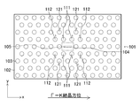
- FIG. 1 is a plan view showing the configuration of the photonic crystal optical resonator according to the embodiment of the present invention.
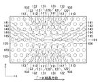
- FIG. 2 is a plan view showing a more detailed structure of the photonic crystal optical resonator according to the embodiment of the present invention.
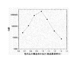
- FIG. 3 is a characteristic diagram showing the result of calculating the relationship between the length (crystal period unit) of the embedded structure 105 and the Q value for the photonic crystal optical resonator having the respective shift amounts shown in Table 1.
- a photonic crystal optical resonator according to an embodiment of the present invention will be described below with reference to FIG.
- this photonic crystal optical resonator includes a base portion 102 and a plurality of columnar lattice elements 103 having a refractive index different from that of the base portion 102.
- the plurality of lattice elements 103 includes plate-shaped photonic crystal bodies 101 that are periodically provided in a lattice pattern on the base 102 at intervals equal to or less than the wavelength of the target light.
- the photonic crystal body 101 is a so-called two-dimensional slab type photonic crystal.
- the lattice element 103 has, for example, a columnar structure. Similar to the embedded structure 105 described later, the refractive index of the lattice element 103 is lower than that of the base 102 and larger than that of air.
- this photonic crystal optical resonator is provided in the photonic crystal body 101, and is provided with an optical confinement portion 104 due to a defect constituted by a portion where the lattice element 103 does not exist at the lattice point of the photonic crystal.
- the light confinement portion 104 is composed of, for example, a point defect in which one photonic crystal lattice element 103 is removed.
- this photonic crystal optical resonator includes an embedded structure 105 in the base portion 102 of the optical confinement portion 104.
- the embedded structure 105 has a longitudinal direction extending in the first direction (x direction) along the ⁇ -K crystal orientation of the photonic crystal formed by the lattice element 103.
- the embedded structure 105 is embedded in the base 102.
- the embedded structure 105 is arranged at the center of the light confinement portion 104 in plan view.
- the refractive index of the embedded structure 105 is lower than that of the base 102 and larger than that of air.
- the embedded structure 105 is composed of water.
- the fundamental resonance mode of the resonator formed by the optical confinement unit 104 is in a state in which the embedded structure 105 has only one antinode of the electric field.
- the length of the embedded structure 105 in the first direction is set to a range of 0.65 to 1.25 times the crystal period.
- the length of the embedded structure 105 in the second direction (y direction) perpendicular to the first direction in plan view is set within a range of 1/20 to 1/8 of the crystal period.
- the longitudinal direction of the embedded structure 105 is the left-right direction of the paper surface.
- an equivalent structure can be obtained by rotating the longitudinal direction by ⁇ 60 degrees from the state shown in FIG. Becomes
- the first lattice element 111 adjacent to the optical confinement unit 104 is arranged in the second direction (y direction) perpendicular to the first direction on the plane where the lattice elements 103 are arranged. , From the lattice point to the side away from the light confinement portion 104 in the second direction.
- the shift amount of the first lattice element 111 is in the range of 0.05 to 0.5 times the crystal period.
- the second lattice element 112 adjacent to the first lattice element 111 in the first direction is shifted from the lattice point to the side away from the light confinement unit 104 in the second direction.
- the amount of shift of the second lattice element 112 is in the range of 0.02 to 0.5 times the crystal period.
- the third lattice element 121 adjacent to the first lattice element 111 and the second lattice element 112 on the side away from the light confinement unit 104 in the second direction has lattice points on the side away from the light confinement unit 104 in the second direction. Have shifted from.
- the shift amount of the third lattice element 121 is in the range of 0.01 to 0.5 times the crystal period.
- the photonic crystal optical resonator can be used as a refractive index sensor because the resonance wavelength and the like are sensitively changed by a minute change in the refractive index in the embedded structure 105. Further, by using the embedded structure 105 on a micro to sub-micro scale, it can be applied as a sensor used for detecting a minute object or a bio-related polymer such as DNA. Further, if a low-refractive index medium having functionality such as optical nonlinear effect and optical amplification is filled in the embedded structure 105 and an optical resonator device using this as an active layer is created, optical material mutual interaction with high Q/V can be achieved. In principle, the enhancement of the action makes it possible to realize a device that operates at a very low energy or a device that is extremely energy efficient.
- the base 102 is made of silicon (refractive index 3.46), and the refractive index of the grating element 103 and the embedded structure 105 is 1.31.
- a clad layer having a refractive index of 1.31 is formed on the upper surface side and the back surface side of the base 102.
- the refractive index of 1.31 corresponds to the refractive index of water or heavy water in the wavelength band of 1.3 to 1.6 ⁇ m used in optical communication.
- the lattice element 103 is a cylindrical through hole, and the radius of this hole is 96 nm.
- the base 102 has a thickness of 220 nm.
- the period a of the photonic crystal is 420 nm.
- the dimensions of the embedded structure 105 on the plane where the lattice elements 103 are arranged are set to the first direction: 410 nm and the second direction: 40 nm.
- the fourth lattice element 141, the fifth lattice element 113, the sixth lattice element 120, the seventh lattice element 122, the The 8th lattice element 131, the 9th lattice element 132, the 10th lattice element 133, the 11th lattice element 142, the 12th lattice element 143, the 13th lattice element 144, and the 14th lattice element 145 are also shifted.
- the grid points are also shifted in the first direction. The amount of each shift is optimized according to the difference in the refractive index between the base portion 102 and the grating element 103 so that the Q value of the resonator is maximized.
- Patent Document 1 a lattice element that does not shift from the lattice point is provided even if it is adjacent to the optical confinement unit 104.
- such a limitation is not provided, and all the above-mentioned lattice elements around the optical confinement portion 104 are targeted, and the shift of the lattice elements for controlling the Q value and the mode volume V is performed.
- the shift of the lattice elements for controlling the Q value and the mode volume V is performed.
- a in the table is the lattice constant of the photonic crystal.
- the shift amounts shown in the table are positive in the direction away from the optical confinement portion 104 (embedded structure 105) which is the center of the resonator. Therefore, the shift closer to the light confining unit 104 is shown as a negative value. Further, “x” indicates the shift amount in the first direction (x direction), and “y” indicates the shift amount in the second direction (y direction).
- This resonance mode has substantially the same properties as the resonance mode of the embedded structure targeted by Patent Document 1, such that only the antinode of one electric field occupying the inside of the embedded structure 105 has a particularly strong electric field strength. Is. However, in the present invention, the light confinement is stronger and the mode volume V becomes half or less.
- Patent Document 1 a large shift to the outside of the resonator is given to the eleventh lattice element 142 to the fourteenth lattice element 145, for example, by giving the eleventh lattice element 142 a shift exceeding 0.1a.
- the eleventh lattice element 142 to the thirteenth lattice element 144 are provided with a shift toward the inside of the resonator in the opposite direction.
- the two are fundamentally different, such as giving a large shift to other lattice elements that are not shifted.
- the shift of the first lattice element 111 and the second lattice element 112 adjacent to the embedded structure 105 has a significant influence on the performance such as the Q value and the mode volume V.
- the shift amounts of the first lattice element 111 and the second lattice element 112 become 0, it becomes difficult to obtain useful Q and mode volume V except for the design of Patent Document 1.
- the third lattice element 121 when the shift in the second direction (y direction) is 0 or the inward direction (negative value), a Q value reduction that cannot be ignored occurs in comparison with the case of the outward shift. To do.
- the low-refractive-index portions (cladding layers) above and below the base 102, excluding the high-refractive-index base 102, are not air but water (refractive index 1.3) or more.
- the shift amounts of the first lattice element 111, the second lattice element 112, and the third lattice element 121 tend to have a large positive value (outward direction).
- FIG. 3 shows the result of calculating the relationship between the length (crystal period unit) of the embedded structure 105 and the Q value for the photonic crystal optical resonator having the respective shift amounts shown in Table 1.
- a Q value of approximately 10,000 or more can be obtained. I understand.
- the base 102 is made of silicon (refractive index 3.46), and the refractive index of the grating element 103 and the embedded structure 105 is 1.45.
- a clad layer having a refractive index of 1.45 is formed on the upper surface side and the rear surface side of the base 102.
- the refractive index of 1.45 corresponds to the refractive index of silicon oxide (SiO 2 ) in the wavelength band of 1.3 to 1.6 ⁇ m used in optical communication.
- the composition of silicon and silicon oxide is a typical material composition in well-known silicon photonics. Therefore, it can be said that this is important in introducing a high Q/V photonic crystal optical resonator into silicon photonics by adjusting the shift amount of each lattice element shown in Table 2.
- the lattice element 103 is a cylindrical through hole, and the radius of this hole is 99 nm.
- the base 102 has a thickness of 220 nm.
- the period a of the photonic crystal is 415 nm.
- the dimensions of the embedded structure 105 on the plane where the lattice elements 103 are arranged are set to the first direction: 390 nm and the second direction: 40 nm.
- the refractive index of the low refractive index medium (SiO 2 ) filling the periphery of the base 102 such as the clad layer, the grating element 103, and the embedded structure 105 is higher, The volume V is being suppressed to a very small value.
- the theoretical Q/V value of the photonic crystal optical resonator due to the shift shown in Table 2 exceeds 50 million. As described above, the present invention can achieve high performance which was difficult to be realized by the conventional photonic crystal optical resonator.
- the shift amount of the first lattice element 111 in the y direction and the shift amount of the second lattice element 112 in the y direction are extremely large. Further, it is important that the shift amount of the second lattice element 112 in the y direction is a positive (outward direction) value that is not small.
- the base 102 is made of silicon (refractive index 3.46), and the grating element 103 and the embedded structure 105 have a refractive index of 1.70.
- a clad layer having a refractive index of 1.70 is formed on the upper surface side and the rear surface side of the base 102.
- This refractive index of 1.70 corresponds to the refractive index of various electro-optic polymer materials in the 1.3-1.6 ⁇ m wavelength band used in optical communication. It can be said that this is important in realizing a photonic crystal optical resonator using an electro-optic polymer as an active medium by adjusting the shift amount of each lattice element shown in Table 3.
- the lattice element 103 is a cylindrical through hole, and the radius of this hole is 92 nm.
- the base 102 has a thickness of 220 nm.
- the period a of the photonic crystal is 390 nm.
- the dimensions of the embedded structure 105 on the plane where the lattice elements 103 are arranged are set to the first direction: 390 nm and the second direction: 40 nm.
- This resonance mode has substantially the same properties as the photonic crystal optical resonator due to the shift shown in Table 1, such that only the antinode of one electric field occupying the embedded structure 105 has a particularly strong electric field strength. ..
- the mode volume V is still as small as about half of ( ⁇ /2n) 3 and the theoretical Q/V value is 10 million. Is over. As described above, according to the present invention, it is possible to achieve high performance which was difficult to realize with the conventional photonic crystal optical resonator.
- the first grating element shifts to the side away from the light confinement portion in the second direction
- the second grating element moves to the side away from the light confinement portion in the second direction
- the third lattice element shifts in the second direction to the side away from the optical confinement portion, so that the mode volume of the resonator is increased even when the refractive index of the low refractive index medium of the photonic crystal is larger than that of air. Can be smaller.
- a longitudinal structure extends in the ⁇ -K crystal orientation direction of a photonic crystal formed by a lattice element, and an embedded structure is provided at the base of an optical confinement portion to obtain a high Q value and a single antinode.
- the photonic crystal optical resonator according to the present invention is a kind of single point defect (H1) optical resonator because the embedded structure is embedded in the single point defect.
- the photonic crystal optical resonator of the present invention realizes a very high Q value and a small mode volume as an H1 resonator, and the low refractive index medium forming the photonic crystal is any substance other than vacuum and air. In some cases, it has features that are particularly effective.
- the shift of the first lattice element, the second lattice element, and the third lattice element to the outside of the resonator plays an important role in the second direction perpendicular to the ⁇ -K crystal orientation. ..
- the fourth grid element, the fifth grid element, the sixth grid element, the seventh grid element, the eighth grid element, the ninth grid element, the tenth grid element, and the eleventh grid element Adjustment is performed to shift the positions of a total of 44 lattice elements of the lattice element, the 12th lattice element, the 13th lattice element, and the 14th lattice element in the first direction and the second direction.
- the shifts of these lattice elements are also effective in increasing the Q value and suppressing the mode volume V of the photonic crystal optical resonator, and it is desirable that the shifts are properly performed without fail.
- the optimum shift amount of each lattice element of the above-mentioned photonic crystal optical resonator varies greatly depending on the dimensions of the embedded structure and the lattice element as well as the refractive index of the material/medium. Most of the shifts of the 44 lattice elements greatly change due to changes in the refractive index and the above dimensions, and the shift amount may be extremely large or almost zero. Furthermore, the direction of the shift may be inside or outside the center of the resonator.
- the low refractive index medium forming the photonic crystal such as the lattice element or the embedded structure is vacuum or air (refractive index 1)
- the first lattice element, the second lattice element, and the third lattice element when the respective shift amounts of the lattice element are set outside the ranges shown in the above-described embodiments, there may be cases where the resonator characteristics become better.
- the medium of the embedded structure is the same as the cladding layers arranged above and below the lattice element and the photonic crystal, but in order to enhance the performance of a specific device, Even if the medium of the embedded structure is replaced with a functional active medium different from the clad layer or the lattice element and filled, the resonance mode having the above-mentioned features of the present invention can be realized.
- the base of the photonic crystal body may be made of Ge, GaAs, InP, GaP, GaN, AlN, SiC, diamond, SiN, etc., which have a refractive index of 2 or more.
- the embedded structure and the lattice element can also be composed of air or vacuum.
- the embedded structure and the grating element can also be made of a low refractive index medium having a refractive index of 1.8 or less.
- Photonic crystal body 102... Base, 103... Lattice element, 104... Optical confinement section, 105... Embedded structure, 111... First lattice element, 112... Second lattice element, 121... Third lattice element.
Landscapes
- Physics & Mathematics (AREA)
- Engineering & Computer Science (AREA)
- Microelectronics & Electronic Packaging (AREA)
- General Physics & Mathematics (AREA)
- Optics & Photonics (AREA)
- Optical Integrated Circuits (AREA)
- Semiconductor Lasers (AREA)
Abstract
第1格子要素(111)は、第2方向に光閉じ込め部(104)より離れる側にシフトしている。また、第2格子要素(112)は、第2方向に光閉じ込め部(104)より離れる側にシフトしている。また、第3格子要素(121)は、第2方向に光閉じ込め部(104)より離れる側にシフトしている。第1格子要素(111)のシフトの量は、結晶周期の0.05~0.5倍の範囲とされている。第2格子要素(112)のシフトの量は、結晶周期の0.02~0.5倍の範囲とされている。第3格子要素(121)のシフトの量は、結晶周期の0.01~0.5倍の範囲とされている。
Description
本発明は、フォトニック結晶光共振器に関する。
フォトニック結晶は、屈折率の異なる2種類以上の媒体からなる周期結晶構造を有する人工素材であり、光の伝播、屈折、反射の制御や光の捕獲などの機能を有している。サブミクロンの結晶周期で構成されるフォトニック結晶により、様々な波長の光を対象とした従来型の光導波路による光集積回路の大幅な小型化、あるいは光デバイスの超小型化、かつ消費エネルギーの大幅な低減が図られることが特に期待される。
これまで、様々な設計で作製されたフォトニック結晶光共振器が提案・開発されてきたが、ここでは、単一点欠陥型光共振器に注目する。フォトニック結晶は、基部と、基部に形成された貫通穴からなる格子要素による周期結晶構造から構成できる。例えば、格子要素を2次元の三角格子に配列した周期結晶構造によりフォトニック結晶(2次元フォトニック結晶)が構成できる。このフォトニック結晶において、格子点から格子要素を取り除いた欠陥による光閉じ込め構造で、共振器が構成できる。格子要素を取り除いた格子点の箇所は、点欠陥と呼ばれている。1つの点欠陥から構成した光閉じ込め構造による共振器は、光閉じ込め構造を中心に、平面視で結晶の6回対称性を有し、H1共振器と呼ばれている。
H1共振器は、フォトニック結晶光共振器の中でも実共振器サイズ(フットプリント)および光学的な体積(モード体積:V)が最も小さい部類に入る。しかし、後述するスロット構造を配置しない場合において、H1共振器のモード体積Vが1(λ/2n)3 を下回る設計はこれまで報告が無い。スロット構造は、光閉じ込め構造における基部に、スロットと呼ばれる例えば直方体状の埋め込み構造体が埋め込まれている構造である。スロット構造におけるスロットは、一般に、200nmを下回る幅が採用されており、光の電界をサブ波長の小さなスロット内に強く閉じ込め、強度を強く増強する効果を有する。このようなスロット構造の性質は、応用上、原子・分子の捕獲、バイオセンサにおける分子やDNAの検出や捕獲、活性媒質の充填による高性能光デバイスの実現などに極めて有用と考えられている。
以上の性質に鑑み、特許文献1に開示された技術では、H1共振器の点欠陥内に収まる長さが短く、かつ幅が非常に狭いスロットを、光閉じ込め構造の部分に配置している。この構成とすることにより、単一点欠陥共振器を維持しながら、H1共振器のモード体積Vを1(λ/2n)3を大幅に下回る設計を可能とした。加えて、特許文献1の技術では、スロットの長手方向の延長線上にある格子要素を、スロットより外側へ格子点からシフトすることでQ値の大幅な増強を可能としている。実際、上述した技術により、Q値が20万、Q/Vが1000万に達する光共振器が実験的に得られている(非特許文献1参照)。
E. Kuramochi, J. K. Kim, H. Taniyama, A. Shinya, S. Kita, and M. Notomi, "Ultrahigh-Q/V single point-defect photonic crystal nanocavity with embedded sub-wavelength air-slot", Conference on Lasers and Electro-Optics OSA Technical Digest (online) (Optical Society of America, 2017), paper JTh3M.5 .https://doi.org/10.1364/CLEO_AT.2017.
杉原 興浩 他、「電気光学ポリマーと光導波路デバイス 有機光デバイス―導波素子から受発光素子まで」、応用物理学会、光学、38巻、12号、598-603頁、2009年。
上述した特許文献1により、サブ波長の寸法のスロット内の1つの電界のアンチノード(antinode)に光を集中し、H1共振器のモード体積Vが1(λ/2n)3を大きく下回り、Q値が10万を大きく上回る設計技術が示された。H1共振器内に、H1共振器を本質的に破壊することない小さなスロットを配置して組み合わせたことが、特許文献1の技術上の最大のポイントであった。特許文献1において、Q値を実用上有用な値に増強するために、スロットの長手方向の延長線上の複数の格子要素を外側方向にシフトする技術が示された。ただし、共振器周囲には上述した技術にしたがって格子点からシフトされる格子要素の他にも多数の格子要素が存在するが、これらの他の格子要素のシフトにより同様のQ値が高くVが小さい共振器が実現されるのかについてはこれまで明らかではなかった。
また、特許文献1の技術では、フォトニック結晶のスロットやフォトニック結晶本体の上下に形成されているクラッド層を構成する低屈折率媒体の屈折率が、1(真空/空気)よりも高い場合でも、Q値およびQ/Vの非常に高い共振器を実現することが可能であった。しかしながら、この技術では、低屈折率媒体の屈折率が空気より高い場合、モード体積Vが大きくなるという問題があった。例えば、低屈折率媒体が水(屈折率1.3)の場合のH1共振器のモード体積Vは、0.06(λ/n)3程度になる。また、シリコン酸化膜(屈折率1.45)の場合のH1共振器のモード体積Vは、0.1(λ/n)3程度とやや大きくなる。特許文献1では、Q値を増強する目的で特定の格子要素をシフトしているので、H1共振器のモード体積Vが大きくなってしまうことについては、考慮されていない。
本発明は、以上のような問題点を解消するためになされたものであり、フォトニック結晶の低屈折率媒体の屈折率が空気より大きい場合であっても、共振器のモード体積がより小さくできるようにすることを目的とする。
本発明に係るフォトニック結晶光共振器は、基部および基部とは異なる屈折率を有する柱状の複数の格子要素を備え、複数の格子要素は、基部上に、対象とする光の波長以下の間隔で格子状に周期的に設けられている板状のフォトニック結晶本体と、フォトニック結晶本体の格子点に格子要素がない部分から構成された欠陥による光閉じ込め部と、格子要素によるフォトニック結晶のΓ-K結晶方位に沿う第1方向に長手方向が延在して、光閉じ込め部の基部に埋め込まれ、基部より屈折率の低い埋め込み構造体とを備え、光閉じ込め部による共振器の共振モードの1つは埋め込み構造体の内部に1つのみの電界のアンチノードを有する状態とされ、埋め込み構造体は、空気より大きい屈折率を有し、格子要素が配列されている平面上で第1方向に垂直な第2方向で、光閉じ込め部に隣り合う第1格子要素は、第2方向に光閉じ込め部より離れる側に格子点からシフトし、第1方向で第1格子要素に隣り合う第2格子要素は、第2方向に光閉じ込め部より離れる側に格子点からシフトし、第2方向に光閉じ込め部より離れる側で、第1格子要素および第2格子要素に隣り合う第3格子要素は、第2方向に光閉じ込め部より離れる側に格子点からシフトし、第1格子要素のシフトの量は、結晶周期の0.05~0.5倍の範囲とされ、第2格子要素のシフトの量は、結晶周期の0.02~0.5倍の範囲とされ、第3格子要素のシフトの量は、結晶周期の0.01~0.5倍の範囲とされている。
上記フォトニック結晶光共振器の一構成例において、第1方向で光閉じ込め部に隣り合う第4格子要素は、第1方向に光閉じ込め部より離れる側にシフトしている。
上記フォトニック結晶光共振器の一構成例において、第1格子要素、第2格子要素、および第3格子要素は、第1方向にシフトしている。
上記フォトニック結晶光共振器の一構成例において、シフトの量は、共振器のQ値が最大となるように、基部と格子要素との間の屈折率の差に合わせて最適化されている。
上記フォトニック結晶光共振器の一構成例において、光閉じ込め部は、フォトニック結晶の格子要素が1つ取り除かれた点欠陥により構成される。
上記フォトニック結晶光共振器の一構成例において、埋め込み構造体の第1方向の長さは、結晶周期の0.65~1.25倍の範囲とされている。
以上説明したことにより、本発明によれば、フォトニック結晶の低屈折率媒体の屈折率が空気より大きい場合であっても、共振器のモード体積がより小さくできる。
以下、本発明の実施の形態に係るフォトニック結晶光共振器について図1を参照して説明する。
このフォトニック結晶光共振器は、まず、基部102および基部102とは異なる屈折率を有する柱状の複数の格子要素103を備える。また、複数の格子要素103が、基部102上に、対象とする光の波長以下の間隔で格子状に周期的に設けられている板状のフォトニック結晶本体101を備える。フォトニック結晶本体101は、いわゆる2次元スラブ型のフォトニック結晶である。格子要素103は、例えば円柱状の構造である。後述する埋め込み構造体105と同様に、格子要素103の屈折率は、基部102の屈折率より低く、空気より大きくされている。
また、このフォトニック結晶光共振器は、フォトニック結晶本体101に設けられて、フォトニック結晶の格子点に格子要素103がない部分から構成された欠陥による光閉じ込め部104を備える。光閉じ込め部104は、例えば、フォトニック結晶の格子要素103が1つ取り除かれた点欠陥により構成されている。
また、このフォトニック結晶光共振器は、光閉じ込め部104における基部102に埋め込み構造体105を備える。埋め込み構造体105は、格子要素103によるフォトニック結晶のΓ-K結晶方位に沿う第1方向(x方向)に、長手方向が延在している。また、埋め込み構造体105は、基部102に埋め込まれて設けられている。埋め込み構造体105は、平面視で光閉じ込め部104の中心に配置されている。
また、埋め込み構造体105の屈折率は、基部102の屈折率より低く、空気より大きくされている。例えば、埋め込み構造体105は、水から構成されている。なお、光閉じ込め部104による共振器の基底共振モードは、埋め込み構造体105の内部に1つのみの電界のアンチノードを有する状態とされている。例えば、埋め込み構造体105の第1方向の長さは、結晶周期の0.65~1.25倍の範囲とされている。また、例えば、埋め込み構造体105の、平面視で第1方向に垂直な第2方向(y方向)の長さは、結晶周期の1/20~1/8の範囲とされている。
図1では、埋め込み構造体105は、長手方向を紙面左右方向としているが、フォトニック結晶の6回対称性より、長手方向を、図1に示す状態より±60度回転させても等価な構造となる。
また、このフォトニック結晶光共振器は、格子要素103が配列されている平面上で第1方向に垂直な第2方向(y方向)で、光閉じ込め部104に隣り合う第1格子要素111は、第2方向に光閉じ込め部104より離れる側に格子点からシフトしている。第1格子要素111のシフトの量は、結晶周期の0.05~0.5倍の範囲とされている。
また、第1方向で第1格子要素111に隣り合う第2格子要素112は、第2方向に光閉じ込め部104より離れる側に格子点からシフトしている。第2格子要素112のシフトの量は、結晶周期の0.02~0.5倍の範囲とされている。
また、第2方向に光閉じ込め部104より離れる側で、第1格子要素111および第2格子要素112に隣り合う第3格子要素121は、第2方向に光閉じ込め部104より離れる側に格子点からシフトしている。第3格子要素121のシフトの量は、結晶周期の0.01~0.5倍の範囲とされている。
以下、実施の形態に係るフォトニック結晶光共振器について、より詳細に説明する。このフォトニック結晶光共振器は、埋め込み構造体105の部分における微小な屈折率変化で、共振波長などが敏感に変化するため、屈折率センサとして用いることができる。また、マイクロ~サブマイクロスケールとした埋め込み構造体105を用いることで、微小な物体、またDNAなどの生体関連高分子の検出に用いるセンサとして応用できる。また、光非線形効果や光増幅などの機能性を有する低屈折率媒体を埋め込み構造体105に充填し、ここを活性層とする光共振器デバイスを作成すれば、高いQ/Vによる光物質相互作用の増強により、特に非常に低エネルギーで動作するデバイスや、極めてエネルギー効率の高いデバイスを実現することが原理的に可能となる。
以下では、基部102をシリコン(屈折率3.46)から構成し、格子要素103および埋め込み構造体105の屈折率1.31とする。また、図示していないが、基部102の上面側および裏面側には、屈折率が1.31のクラッド層が形成されているものとする。この屈折率1.31は、光通信で用いられている1.3-1.6μmの波長帯における、水や重水の屈折率に相当する。
また、格子要素103は、円柱形状の貫通穴とし、この穴の半径は96nmとする。また、基部102は、厚さ220nmとする。また、フォトニック結晶の周期aは、420nmとする。また、格子要素103が配列されている平面上における埋め込み構造体105の寸法を、第1方向:410nm、第2方向:40nmとする。
また、以下では、第1格子要素111、第2格子要素112、第3格子要素121に加え、第4格子要素141、第5格子要素113、第6格子要素120、第7格子要素122、第8格子要素131、第9格子要素132、第10格子要素133、第11格子要素142、第12格子要素143、第13格子要素144、第14格子要素145についても、シフトの対象とする。また、第2方向に加え、第1方向にも格子点からシフトさせる。各シフトの量は、共振器のQ値が最大となるように、基部102と格子要素103との間の屈折率の差に合わせて最適化する。
特許文献1では、光閉じ込め部104に隣り合っていても、格子点からシフトしない格子要素を設けている。これに対し、本発明においては、そのような制限を設けず、光閉じ込め部104の周囲の上述した全ての格子要素を対象とし、Q値やモード体積Vを制御するための格子要素のシフトの調整を検討した。この検討において、電磁界解析により、以下の表1~3に示す各格子要素のシフト量の調整により、有用な共振器性能が得られることを見いだした。
なお、表中のaは、フォトニック結晶の格子定数である。また、表に示すシフト量は、共振器中心である光閉じ込め部104(埋め込み構造体105)より離れる方向のシフト量を正としている。したがって、光閉じ込め部104に近づけるシフトは、負の値として示している。また、「x」は、第1方向(x方向)へのシフト量を示し、「y」は、第2方向(y方向)へのシフト量を示している。

表1に示すシフトにより調整されたフォトニック結晶光共振器の共振モードは、電磁界解析によりQ値が200万、モード体積V=0.028(λ/n)3を、共振モード波長1578nmにて示した。この共振モードは、埋め込み構造体105の内部を占める1つの電界のアンチノードのみが特に強い電界強度を有するなど、特許文献1の対象とする埋め込み構造体の共振モードとほぼ同等の性質を有するものである。ただし、本発明の方が、光閉じ込めがより強く、モード体積Vが半分以下になる。
また、特許文献1では第11格子要素142に0.1aを超えるシフトを与えるなど、第11格子要素142~第14格子要素145に対して共振器外側への大きなシフトを与えている。これに対し、表1に示すシフトでは、第11格子要素142から第13格子要素144には、逆方向の共振器内側へのシフトを与えている。一方、特許文献1ではシフトしていない他の格子要素に大きなシフトを与えるなど、両者は根本的に異なっている。
表1に示す各シフト量において、特に埋め込み構造体105に隣り合う第1格子要素111および第2格子要素112のシフトは、Q値やモード体積Vのなどの性能におよぼす影響は重大である。例えば、第1格子要素111,第2格子要素112のシフト量が0になると、特許文献1の設計を除けば有用なQおよびモード体積Vを得ることが困難になる。また、第3格子要素121については、第2方向(y方向)へのシフトが、0か内側方向(負の値)になると、外側へのシフトする場合に対して無視できないQ値減少が発生する。以下の表2,表3にも示すように、高屈折率の基部102を除く、基部102の上下の低屈折率部分(クラッド層)が空気ではなく、水(屈折率1.3)やより高い屈折率の媒質である場合、第1格子要素111,第2格子要素112,第3格子要素121のシフト量は、正(外側方向)の大きな値になる傾向がある。
図3に、表1に示す各シフト量としたフォトニック結晶光共振器について、埋め込み構造体105の長さ(結晶周期単位)とQ値との関係を計算した結果を示す。図3に示すように、埋め込み構造体105の第1方向の長さを、結晶周期の0.65~1.25倍の範囲とすることで、概ね1万を超えるQ値が得られることが分かる。
次に、表2を用いて説明する。表2では、基部102をシリコン(屈折率3.46)から構成し、格子要素103および埋め込み構造体105の屈折率1.45とする。また、図示していないが、基部102の上面側および裏面側には、屈折率が1.45のクラッド層が形成されているものとする。この屈折率1.45は、光通信で用いられている1.3-1.6μmの波長帯における、酸化シリコン(SiO2)の屈折率に相当する。シリコンと酸化シリコンの構成は、よく知られたシリコンフォトニクスにおける代表的な材料構成である。したがって、表2に示す各格子要素のシフト量の調整により、シリコンフォトニクスに高Q/Vのフォトニック結晶光共振器を導入するうえで重要なものであるといえる。
表2では、格子要素103は、円柱形状の貫通穴とし、この穴の半径は99nmとする。また、基部102は、厚さ220nmとする。また、フォトニック結晶の周期aは、415nmとする。また、格子要素103が配列されている平面上における埋め込み構造体105の寸法を、第1方向:390nm、第2方向:40nmとする。
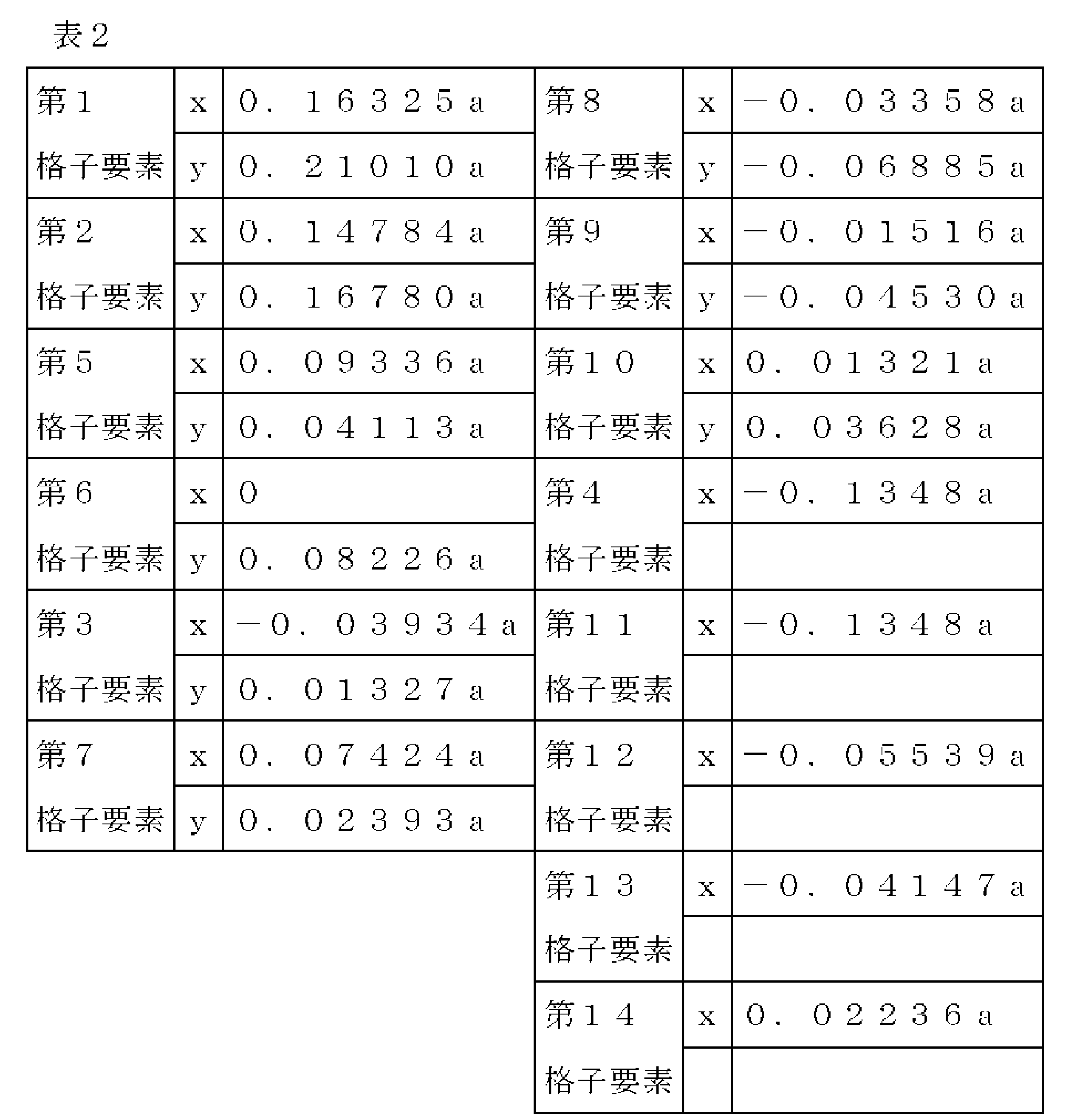
表2に示すシフトにより調整されたフォトニック結晶光共振器の共振モードは、電磁界解析によりQ値180万、モード体積V=0.032(λ/n)3を共振モード波長1578nmにて示した。この共振モードは、埋め込み構造体105を占める1つの電界のアンチノードのみが特に強い電界強度を有するなど、表1に示したシフトによるフォトニック結晶光共振器とほぼ同等の性質を有するものである。
注目すべきは、クラッド層などの基部102の周囲や、格子要素103や、埋め込み構造体105を充たす低屈折率媒体(SiO2)の屈折率が更に高くなっているのにもかかわらず、モード体積Vが極めて小さく抑制されているところである。表2に示すシフトによるフォトニック結晶光共振器の理論上のQ/V値は、5千万を超えている。このように従来のフォトニック結晶光共振器では実現が困難であった高性能が、本発明により達成可能となる。
また、表2に示すシフトにより調整されたフォトニック結晶光共振器においても、第1格子要素111のy方向へのシフト量、第2格子要素112のy方向へのシフト量が極めて大きい。また、第2格子要素112のy方向へのシフト量は正(外側方向)の小さくない値になることは重要である。
次に、表3を用いて説明する。表3では、基部102をシリコン(屈折率3.46)から構成し、格子要素103および埋め込み構造体105の屈折率1.70とする。また、図示していないが、基部102の上面側および裏面側には、屈折率が1.70のクラッド層が形成されているものとする。この屈折率1.70は、光通信で用いられている1.3-1.6μmの波長帯における、様々な電気光学ポリマー材料の屈折率に相当する。表3に示す各格子要素のシフト量の調整により、電気光学ポリマーを活性媒質として用いるフォトニック結晶光共振器を実現するうえで重要なものであるといえる。
表3では、格子要素103は、円柱形状の貫通穴とし、この穴の半径は92nmとする。また、基部102は、厚さ220nmとする。また、フォトニック結晶の周期aは、390nmとする。また、格子要素103が配列されている平面上における埋め込み構造体105の寸法を、第1方向:390nm、第2方向:40nmとする。
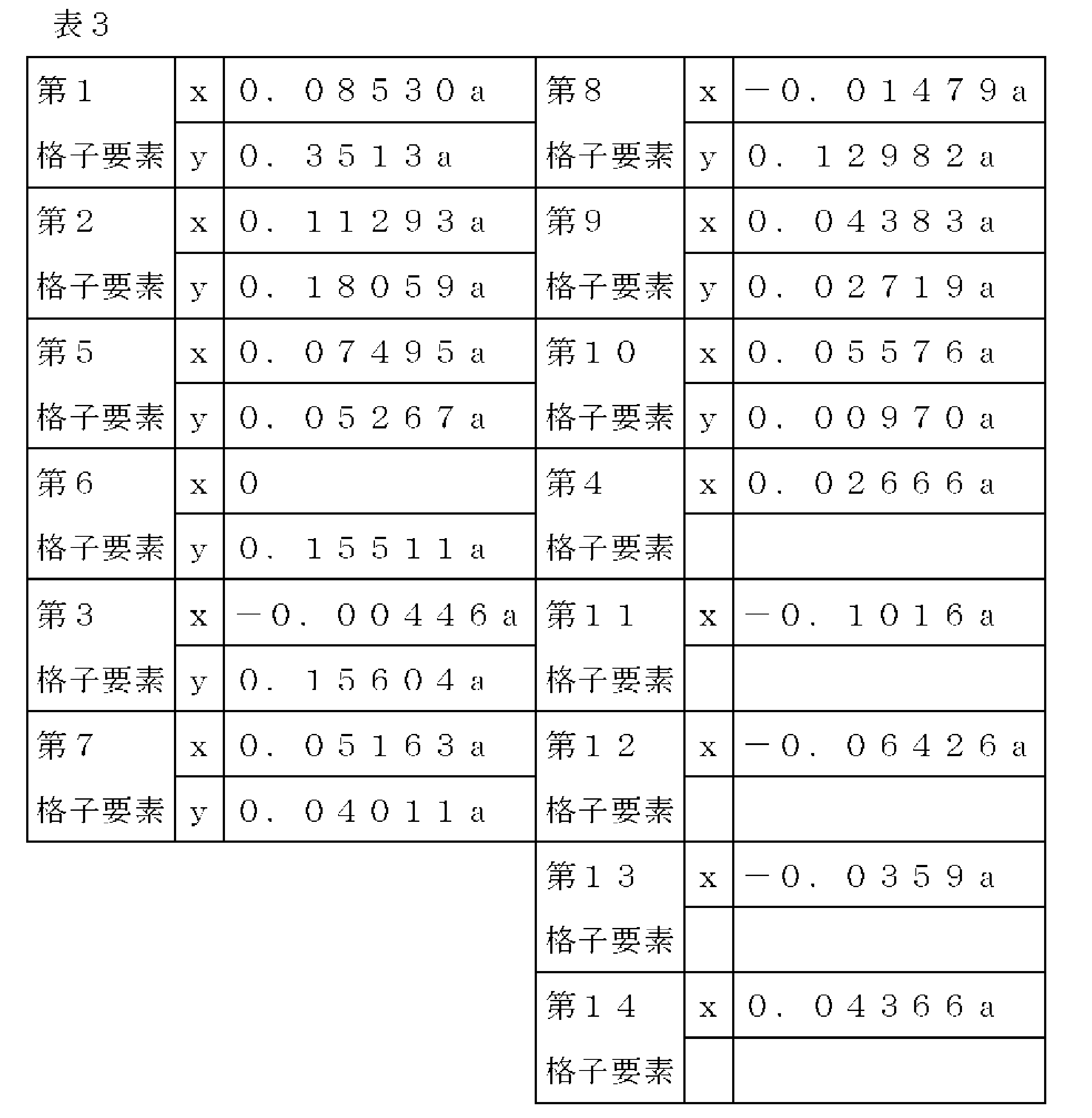
表3に示すシフトにより調整されたフォトニック結晶光共振器の共振モードは、電磁界解析によりQ値は80万、モード体積V=0.063(λ/n)3を共振モード波長1565nmにて示した。この共振モードは、埋め込み構造体105を占める1つの電界のアンチノードのみが特に強い電界強度を有するなど、表1に示したシフトによるフォトニック結晶光共振器とほぼ同等の性質を有するものである。低屈折率媒体(電気光学ポリマー)の屈折率が非常に高いのもかかわらず、モード体積Vは(λ/2n)3の半分程度となお極めて小さく、理論上のQ/V値は1千万を超えている。このように従来のフォトニック結晶光共振器では実現が困難であった高性能が、本発明によれば達成可能となる。
また、表3に示すシフトにより調整されたフォトニック結晶光共振器においても、第1格子要素111のy方向へのシフト量、第2格子要素112のy方向へのシフト量、および第3格子要素121のy方向へのシフト量が極めて大きい。これらのシフトが、フォトニック結晶光共振器のQ値の増大に重要な役割を果たしている。
以上に説明したように、本発明によれば、第1格子要素は、第2方向に光閉じ込め部より離れる側にシフトし、第2格子要素は、第2方向に光閉じ込め部より離れる側にシフトし、第3格子要素は、第2方向に光閉じ込め部より離れる側にシフトするので、フォトニック結晶の低屈折率媒体の屈折率が空気より大きい場合であっても、共振器のモード体積がより小さくできる。
本発明によれば、格子要素によるフォトニック結晶のΓ-K結晶方位方向に長手方向が延在して光閉じ込め部における基部に、埋め込み構造体を設け、高いQ値と単一のアンチノードへの電界集中とが両立できる2次元フォトニック結晶光共振器を、特許文献1とは異なる特定の格子要素の外側へのシフトと組み合わせることにより、より高い光閉じ込め効果を伴って得られる。
本発明によるフォトニック結晶光共振器は、埋め込み構造体が単一点欠陥内に埋め込まれているため、単一点欠陥(H1)光共振器の一種である。本発明のフォトニック結晶光共振器は、H1共振器としては非常に高いQ値と小さなモード体積が実現され、フォトニック結晶を構成する低屈折率媒体が真空・空気以外の任意の物質である場合において、特に有効である特徴を有する。本発明では、第1格子要素、第2格子要素、第3格子要素の、Γ-K結晶方位に垂直な第2方向で、共振器外側へのシフトが重要な役割を果たしていることを提示した。
また、表1~表3では、他にも、第4格子要素、第5格子要素、第6格子要素、第7格子要素、第8格子要素、第9格子要素、第10格子要素、第11格子要素、第12格子要素、第13格子要素、第14格子要素の合計44個の格子要素の位置を第1方向、第2方向にシフトする調整を実施している。これらの格子要素のシフトも、フォトニック結晶光共振器のQ値の増大やモード体積Vの抑制に効果があり、欠くことなく適切にシフトされることが望ましい。
ただし、上述したフォトニック結晶光共振器の、各格子要素の最適なシフト量は、材料・媒質の屈折率はもとより、埋め込み構造体や格子要素の寸法にも依存して大きく変化する。44個の格子要素のシフトのうち大部分は、屈折率や上記寸法が変化することにより大きく変化し、シフト量が極めて大きくなることもあれば、ほぼ0になることもある。更には、シフトの向きが共振器中心に対し内側になることもあれば外側になることもある。
どのようなシフトを与えるべきかは、フォトニック結晶の各部寸法や屈折率に大きく依存するため、経験的知見を得ることが困難である。一方で、本発明では、第1格子要素、第2格子要素、第3格子要素の各シフトについては、フォトニック結晶各部寸法や屈折率に関わらずに常に有用な効果が得られる。一方、第1格子要素、第2格子要素、第3格子要素について、本発明によるシフト量としない場合は、光共振器の性能が大きく損なわれる。
本発明において、格子要素や埋め込み構造体などのフォトニック結晶を構成する低屈折率媒体が、真空または空気(屈折率1)である場合においては、第1格子要素、第2格子要素、第3格子要素の各シフト量は、上述した実施の形態に示した範囲外に設定すると、共振器特性がより良好になる場合が存在しうる。
表1~表3に示した各シフト量において、埋め込み構造体の媒質は、格子要素やフォトニック結晶の上下に配置するクラッド層と同一であるが、特定のデバイスの性能を増強するために、埋め込み構造体の媒質を、クラッド層や格子要素とは異なる機能性活性媒質に置き換えて充填しても、上述した本発明の特徴を有する共振モードが実現可能である。
なお、本発明は以上に説明した実施の形態に限定されるものではなく、本発明の技術的思想内で、当分野において通常の知識を有する者により、多くの変形および組み合わせが実施可能であることは明白である。
例えば、フォトニック結晶本体の基部は、2以上の屈折率を有するGe,GaAs,InP,GaP,GaN,AlN,SiC,ダイヤモンド、SiNなどから構成することもできる。また、埋め込み構造体および格子要素は、空気、真空から構成することもできる。また、埋め込み構造体および格子要素は、屈折率1.8以下の低屈折率媒体から構成することもできる。
101…フォトニック結晶本体、102…基部、103…格子要素、104…光閉じ込め部、105…埋め込み構造体、111…第1格子要素、112…第2格子要素、121…第3格子要素。
Claims (6)
- 基部および前記基部とは異なる屈折率を有する柱状の複数の格子要素を備え、前記複数の格子要素は、前記基部上に、対象とする光の波長以下の間隔で格子状に周期的に設けられている板状のフォトニック結晶本体と、
前記フォトニック結晶本体の格子点に前記格子要素がない部分から構成された欠陥による光閉じ込め部と、
前記格子要素によるフォトニック結晶のΓ-K結晶方位に沿う第1方向に長手方向が延在して、前記光閉じ込め部の前記基部に埋め込まれ、前記基部より屈折率の低い埋め込み構造体と
を備え、
前記光閉じ込め部による共振器の共振モードの1つは前記埋め込み構造体の内部に1つのみの電界のアンチノードを有する状態とされ、
前記埋め込み構造体は、空気より大きい屈折率を有し、
前記格子要素が配列されている平面上で前記第1方向に垂直な第2方向で、前記光閉じ込め部に隣り合う第1格子要素は、前記第2方向に前記光閉じ込め部より離れる側に格子点からシフトし、
前記第1方向で前記第1格子要素に隣り合う第2格子要素は、前記第2方向に前記光閉じ込め部より離れる側に格子点からシフトし、
前記第2方向に前記光閉じ込め部より離れる側で、前記第1格子要素および前記第2格子要素に隣り合う第3格子要素は、前記第2方向に前記光閉じ込め部より離れる側に格子点からシフトし、
前記第1格子要素のシフトの量は、結晶周期の0.05~0.5倍の範囲とされ、
前記第2格子要素のシフトの量は、結晶周期の0.02~0.5倍の範囲とされ、
前記第3格子要素のシフトの量は、結晶周期の0.01~0.5倍の範囲とされ
ていること特徴とするフォトニック結晶光共振器。 - 請求項1記載のフォトニック結晶光共振器において、
前記第1方向で前記光閉じ込め部に隣り合う第4格子要素は、前記第1方向に前記光閉じ込め部より離れる側にシフトしていることを特徴とするフォトニック結晶光共振器。 - 請求項1または2記載のフォトニック結晶光共振器において、
前記第1格子要素、前記第2格子要素、および前記第3格子要素は、前記第1方向にシフトしていることを特徴とするフォトニック結晶光共振器。 - 請求項3記載のフォトニック結晶光共振器において、
シフトの量は、共振器のQ値が最大となるように、前記基部と前記格子要素との間の屈折率の差に合わせて最適化されていることを特徴とするフォトニック結晶光共振器。 - 請求項1~4のいずれか1項に記載のフォトニック結晶光共振器において、
前記光閉じ込め部は、フォトニック結晶の前記格子要素が1つ取り除かれた点欠陥により構成されることを特徴とするフォトニック結晶光共振器。 - 請求項1~5のいずれか1項に記載のフォトニック結晶光共振器において、
前記埋め込み構造体の前記第1方向の長さは、結晶周期の0.65~1.25倍の範囲とされていることを特徴とするフォトニック結晶光共振器。
Priority Applications (1)
| Application Number | Priority Date | Filing Date | Title |
|---|---|---|---|
| US17/431,013 US11747558B2 (en) | 2019-02-18 | 2020-02-04 | Photonic crystal optical resonator |
Applications Claiming Priority (2)
| Application Number | Priority Date | Filing Date | Title |
|---|---|---|---|
| JP2019-026454 | 2019-02-18 | ||
| JP2019026454A JP7124752B2 (ja) | 2019-02-18 | 2019-02-18 | フォトニック結晶光共振器 |
Publications (1)
| Publication Number | Publication Date |
|---|---|
| WO2020170795A1 true WO2020170795A1 (ja) | 2020-08-27 |
Family
ID=72144695
Family Applications (1)
| Application Number | Title | Priority Date | Filing Date |
|---|---|---|---|
| PCT/JP2020/004040 Ceased WO2020170795A1 (ja) | 2019-02-18 | 2020-02-04 | フォトニック結晶光共振器 |
Country Status (3)
| Country | Link |
|---|---|
| US (1) | US11747558B2 (ja) |
| JP (1) | JP7124752B2 (ja) |
| WO (1) | WO2020170795A1 (ja) |
Families Citing this family (1)
| Publication number | Priority date | Publication date | Assignee | Title |
|---|---|---|---|---|
| JP7139990B2 (ja) * | 2019-02-14 | 2022-09-21 | 日本電信電話株式会社 | フォトニック結晶光共振器 |
Citations (4)
| Publication number | Priority date | Publication date | Assignee | Title |
|---|---|---|---|---|
| JP2004245866A (ja) * | 2003-02-10 | 2004-09-02 | Univ Kyoto | 2次元フォトニック結晶中の共振器と波長分合波器 |
| US20060067605A1 (en) * | 2004-09-30 | 2006-03-30 | Laura Wills Mirkarimi | Photonic crystal optical temperature measuring system |
| JP2016154163A (ja) * | 2015-02-20 | 2016-08-25 | 日本電信電話株式会社 | フォトニック結晶共振器およびその設計方法 |
| JP2018132726A (ja) * | 2017-02-17 | 2018-08-23 | 日本電信電話株式会社 | フォトニック結晶光共振器 |
Family Cites Families (3)
| Publication number | Priority date | Publication date | Assignee | Title |
|---|---|---|---|---|
| JP4870706B2 (ja) * | 2008-03-26 | 2012-02-08 | 日本電信電話株式会社 | 光双安定素子及びメモリ安定化方法 |
| US20130042679A1 (en) * | 2011-08-16 | 2013-02-21 | The Johns Hopkins University | Chip-Scale Optomechanical Gravimeter |
| JP6251159B2 (ja) * | 2014-12-15 | 2017-12-20 | 日本電信電話株式会社 | 光素子 |
-
2019
- 2019-02-18 JP JP2019026454A patent/JP7124752B2/ja active Active
-
2020
- 2020-02-04 WO PCT/JP2020/004040 patent/WO2020170795A1/ja not_active Ceased
- 2020-02-04 US US17/431,013 patent/US11747558B2/en active Active
Patent Citations (4)
| Publication number | Priority date | Publication date | Assignee | Title |
|---|---|---|---|---|
| JP2004245866A (ja) * | 2003-02-10 | 2004-09-02 | Univ Kyoto | 2次元フォトニック結晶中の共振器と波長分合波器 |
| US20060067605A1 (en) * | 2004-09-30 | 2006-03-30 | Laura Wills Mirkarimi | Photonic crystal optical temperature measuring system |
| JP2016154163A (ja) * | 2015-02-20 | 2016-08-25 | 日本電信電話株式会社 | フォトニック結晶共振器およびその設計方法 |
| JP2018132726A (ja) * | 2017-02-17 | 2018-08-23 | 日本電信電話株式会社 | フォトニック結晶光共振器 |
Non-Patent Citations (2)
| Title |
|---|
| KURAMOCHI,EIICHI ET AL.: "Slot effect in ultrahigh Q/V Hl photonic crystal nanocavities with a subwavelength slot.", JSAP AUTUMN MEETING 2017, 25 August 2017 (2017-08-25), XP055734240 * |
| MINKOV, M. ET AL.: "Automated optimization of photonic crystal slab cavities", SCIENTIFIC REPORTS, vol. 4, no. 5124, 30 May 2014 (2014-05-30), pages 1 - 8, XP055675129, DOI: 10.1038/srep05124 * |
Also Published As
| Publication number | Publication date |
|---|---|
| JP7124752B2 (ja) | 2022-08-24 |
| US11747558B2 (en) | 2023-09-05 |
| JP2020134646A (ja) | 2020-08-31 |
| US20220075116A1 (en) | 2022-03-10 |
Similar Documents
| Publication | Publication Date | Title |
|---|---|---|
| JP5188009B2 (ja) | 3次元周期構造及びそれを有する機能素子および発光素子 | |
| JP4612844B2 (ja) | 3次元周期構造及びそれを有する機能素子 | |
| CN1875303A (zh) | 电磁波频率滤波器 | |
| US20170082842A1 (en) | Ultra-small cavity with reflecting metasurfaces | |
| CN105576384A (zh) | 一种多通道可调谐Tamm等离子体完美吸收器 | |
| Subashiev et al. | Modal control in semiconductor optical waveguides with uniaxially patterned layers | |
| WO2020170795A1 (ja) | フォトニック結晶光共振器 | |
| WO2007027982A2 (en) | Devices and methods for providing stimulated raman lasing | |
| CN110618486B (zh) | 基于对称三波导与亚波长结构的偏振无关的功率分配器 | |
| JP7389263B2 (ja) | 光走査素子 | |
| JP7782559B2 (ja) | 光デバイス | |
| JP4684861B2 (ja) | 導波路及びそれを有するデバイス | |
| Park et al. | Optical properties of superlattice photonic crystal waveguides | |
| JP2024177334A (ja) | 光走査素子 | |
| JP4964726B2 (ja) | 光共振器構造 | |
| CN111175871B (zh) | 一种基于近对称保护型连续束缚态的亚波长光栅结构 | |
| JP6162665B2 (ja) | フォトニック結晶共振器 | |
| JP6317278B2 (ja) | フォトニック結晶共振器の設計方法 | |
| Kim et al. | Nano stepping-stone laser | |
| Kumar et al. | Widely tunable mirror based on 3D hollow waveguide for tunable photonic integrated circuits | |
| WO2022019143A1 (ja) | 光走査素子 | |
| Zhen et al. | A novel application of two-dimensional photonic crystals: polarization beam splitter | |
| JP7675657B2 (ja) | フォトニック結晶素子用複合基板およびフォトニック結晶素子 | |
| CN111061008A (zh) | 一种结构缺陷为“d”形空气孔的平板光子晶体微腔 | |
| Parker et al. | InP/InGaAsP flattened ring lasers with low-loss etched beam splitters |
Legal Events
| Date | Code | Title | Description |
|---|---|---|---|
| 121 | Ep: the epo has been informed by wipo that ep was designated in this application |
Ref document number: 20758788 Country of ref document: EP Kind code of ref document: A1 |
|
| NENP | Non-entry into the national phase |
Ref country code: DE |
|
| 122 | Ep: pct application non-entry in european phase |
Ref document number: 20758788 Country of ref document: EP Kind code of ref document: A1 |