WO2020170535A1 - 半導体基板および半導体モジュール - Google Patents
半導体基板および半導体モジュール Download PDFInfo
- Publication number
- WO2020170535A1 WO2020170535A1 PCT/JP2019/046006 JP2019046006W WO2020170535A1 WO 2020170535 A1 WO2020170535 A1 WO 2020170535A1 JP 2019046006 W JP2019046006 W JP 2019046006W WO 2020170535 A1 WO2020170535 A1 WO 2020170535A1
- Authority
- WO
- WIPO (PCT)
- Prior art keywords
- protective material
- glass substrate
- semiconductor substrate
- corner portion
- semiconductor
- Prior art date
- Legal status (The legal status is an assumption and is not a legal conclusion. Google has not performed a legal analysis and makes no representation as to the accuracy of the status listed.)
- Ceased
Links
Images

Classifications
-
- H—ELECTRICITY
- H10—SEMICONDUCTOR DEVICES; ELECTRIC SOLID-STATE DEVICES NOT OTHERWISE PROVIDED FOR
- H10W—GENERIC PACKAGES, INTERCONNECTIONS, CONNECTORS OR OTHER CONSTRUCTIONAL DETAILS OF DEVICES COVERED BY CLASS H10
- H10W76/00—Containers; Fillings or auxiliary members therefor; Seals
- H10W76/60—Seals
-
- C—CHEMISTRY; METALLURGY
- C03—GLASS; MINERAL OR SLAG WOOL
- C03C—CHEMICAL COMPOSITION OF GLASSES, GLAZES OR VITREOUS ENAMELS; SURFACE TREATMENT OF GLASS; SURFACE TREATMENT OF FIBRES OR FILAMENTS MADE FROM GLASS, MINERALS OR SLAGS; JOINING GLASS TO GLASS OR OTHER MATERIALS
- C03C17/00—Surface treatment of glass, not in the form of fibres or filaments, by coating
- C03C17/28—Surface treatment of glass, not in the form of fibres or filaments, by coating with organic material
- C03C17/32—Surface treatment of glass, not in the form of fibres or filaments, by coating with organic material with synthetic or natural resins
-
- H—ELECTRICITY
- H10—SEMICONDUCTOR DEVICES; ELECTRIC SOLID-STATE DEVICES NOT OTHERWISE PROVIDED FOR
- H10W—GENERIC PACKAGES, INTERCONNECTIONS, CONNECTORS OR OTHER CONSTRUCTIONAL DETAILS OF DEVICES COVERED BY CLASS H10
- H10W42/00—Arrangements for protection of devices
- H10W42/121—Arrangements for protection of devices protecting against mechanical damage
-
- H—ELECTRICITY
- H10—SEMICONDUCTOR DEVICES; ELECTRIC SOLID-STATE DEVICES NOT OTHERWISE PROVIDED FOR
- H10W—GENERIC PACKAGES, INTERCONNECTIONS, CONNECTORS OR OTHER CONSTRUCTIONAL DETAILS OF DEVICES COVERED BY CLASS H10
- H10W70/00—Package substrates; Interposers; Redistribution layers [RDL]
- H10W70/60—Insulating or insulated package substrates; Interposers; Redistribution layers
- H10W70/67—Insulating or insulated package substrates; Interposers; Redistribution layers characterised by their insulating layers or insulating parts
- H10W70/68—Shapes or dispositions thereof
-
- H—ELECTRICITY
- H10—SEMICONDUCTOR DEVICES; ELECTRIC SOLID-STATE DEVICES NOT OTHERWISE PROVIDED FOR
- H10W—GENERIC PACKAGES, INTERCONNECTIONS, CONNECTORS OR OTHER CONSTRUCTIONAL DETAILS OF DEVICES COVERED BY CLASS H10
- H10W76/00—Containers; Fillings or auxiliary members therefor; Seals
- H10W76/10—Containers or parts thereof
- H10W76/12—Containers or parts thereof characterised by their shape
- H10W76/15—Containers comprising an insulating or insulated base
-
- H—ELECTRICITY
- H10—SEMICONDUCTOR DEVICES; ELECTRIC SOLID-STATE DEVICES NOT OTHERWISE PROVIDED FOR
- H10W—GENERIC PACKAGES, INTERCONNECTIONS, CONNECTORS OR OTHER CONSTRUCTIONAL DETAILS OF DEVICES COVERED BY CLASS H10
- H10W76/00—Containers; Fillings or auxiliary members therefor; Seals
- H10W76/10—Containers or parts thereof
- H10W76/17—Containers or parts thereof characterised by their materials
-
- H—ELECTRICITY
- H05—ELECTRIC TECHNIQUES NOT OTHERWISE PROVIDED FOR
- H05K—PRINTED CIRCUITS; CASINGS OR CONSTRUCTIONAL DETAILS OF ELECTRIC APPARATUS; MANUFACTURE OF ASSEMBLAGES OF ELECTRICAL COMPONENTS
- H05K1/00—Printed circuits
- H05K1/02—Details
- H05K1/03—Use of materials for the substrate
- H05K1/0306—Inorganic insulating substrates, e.g. ceramic, glass
-
- H—ELECTRICITY
- H05—ELECTRIC TECHNIQUES NOT OTHERWISE PROVIDED FOR
- H05K—PRINTED CIRCUITS; CASINGS OR CONSTRUCTIONAL DETAILS OF ELECTRIC APPARATUS; MANUFACTURE OF ASSEMBLAGES OF ELECTRICAL COMPONENTS
- H05K2201/00—Indexing scheme relating to printed circuits covered by H05K1/00
- H05K2201/09—Shape and layout
- H05K2201/09009—Substrate related
- H05K2201/09027—Non-rectangular flat PCB, e.g. circular
-
- H—ELECTRICITY
- H05—ELECTRIC TECHNIQUES NOT OTHERWISE PROVIDED FOR
- H05K—PRINTED CIRCUITS; CASINGS OR CONSTRUCTIONAL DETAILS OF ELECTRIC APPARATUS; MANUFACTURE OF ASSEMBLAGES OF ELECTRICAL COMPONENTS
- H05K2201/00—Indexing scheme relating to printed circuits covered by H05K1/00
- H05K2201/09—Shape and layout
- H05K2201/09145—Edge details
- H05K2201/09154—Bevelled, chamferred or tapered edge
-
- H—ELECTRICITY
- H10—SEMICONDUCTOR DEVICES; ELECTRIC SOLID-STATE DEVICES NOT OTHERWISE PROVIDED FOR
- H10F—INORGANIC SEMICONDUCTOR DEVICES SENSITIVE TO INFRARED RADIATION, LIGHT, ELECTROMAGNETIC RADIATION OF SHORTER WAVELENGTH OR CORPUSCULAR RADIATION
- H10F39/00—Integrated devices, or assemblies of multiple devices, comprising at least one element covered by group H10F30/00, e.g. radiation detectors comprising photodiode arrays
- H10F39/80—Constructional details of image sensors
- H10F39/804—Containers or encapsulations
-
- H—ELECTRICITY
- H10—SEMICONDUCTOR DEVICES; ELECTRIC SOLID-STATE DEVICES NOT OTHERWISE PROVIDED FOR
- H10F—INORGANIC SEMICONDUCTOR DEVICES SENSITIVE TO INFRARED RADIATION, LIGHT, ELECTROMAGNETIC RADIATION OF SHORTER WAVELENGTH OR CORPUSCULAR RADIATION
- H10F39/00—Integrated devices, or assemblies of multiple devices, comprising at least one element covered by group H10F30/00, e.g. radiation detectors comprising photodiode arrays
- H10F39/80—Constructional details of image sensors
- H10F39/805—Coatings
- H10F39/8057—Optical shielding
-
- H—ELECTRICITY
- H10—SEMICONDUCTOR DEVICES; ELECTRIC SOLID-STATE DEVICES NOT OTHERWISE PROVIDED FOR
- H10F—INORGANIC SEMICONDUCTOR DEVICES SENSITIVE TO INFRARED RADIATION, LIGHT, ELECTROMAGNETIC RADIATION OF SHORTER WAVELENGTH OR CORPUSCULAR RADIATION
- H10F39/00—Integrated devices, or assemblies of multiple devices, comprising at least one element covered by group H10F30/00, e.g. radiation detectors comprising photodiode arrays
- H10F39/80—Constructional details of image sensors
- H10F39/806—Optical elements or arrangements associated with the image sensors
-
- H—ELECTRICITY
- H10—SEMICONDUCTOR DEVICES; ELECTRIC SOLID-STATE DEVICES NOT OTHERWISE PROVIDED FOR
- H10W—GENERIC PACKAGES, INTERCONNECTIONS, CONNECTORS OR OTHER CONSTRUCTIONAL DETAILS OF DEVICES COVERED BY CLASS H10
- H10W70/00—Package substrates; Interposers; Redistribution layers [RDL]
- H10W70/60—Insulating or insulated package substrates; Interposers; Redistribution layers
- H10W70/67—Insulating or insulated package substrates; Interposers; Redistribution layers characterised by their insulating layers or insulating parts
- H10W70/69—Insulating materials thereof
- H10W70/692—Ceramics or glasses
-
- H—ELECTRICITY
- H10—SEMICONDUCTOR DEVICES; ELECTRIC SOLID-STATE DEVICES NOT OTHERWISE PROVIDED FOR
- H10W—GENERIC PACKAGES, INTERCONNECTIONS, CONNECTORS OR OTHER CONSTRUCTIONAL DETAILS OF DEVICES COVERED BY CLASS H10
- H10W90/00—Package configurations
- H10W90/701—Package configurations characterised by the relative positions of pads or connectors relative to package parts
Definitions
- the present technology relates to semiconductor substrates. More specifically, the present invention relates to a semiconductor substrate and a semiconductor module protection structure using a glass substrate.
- the image sensor Due to the higher functionality and larger size of the image sensor, if it is mounted using an organic substrate or a ceramic substrate as in the past, the image sensor may rise due to warpage, or it may be connected due to the difference in thermal expansion coefficient. The reliability may not be maintained. Therefore, it is required to employ a glass substrate that ensures evenness. On the other hand, since the glass substrate is fragile and is easily damaged by an impact during transportation, it is necessary to protect the outer peripheral portion of the substrate with resin or the like. In this glass substrate, the end face is particularly fragile, and, for example, a manufacturing method for forming a thick protective layer on the end face has been proposed (for example, refer to Patent Document 1).
- an etching resistant layer is provided, and a space surrounded by the etching resistant layer and the side surface of the glass substrate is filled with a polymer agent for end face protection, so that the protective layer is formed in the direction outside the side surface of the glass substrate. Has formed.
- this conventional technique requires a step of peeling after forming the etching resistant layer, and the substrate may be warped due to the contraction of the protective layer.
- the present technology was created in view of such circumstances, and its purpose is to provide a protective structure that appropriately protects the side surface of the glass substrate.
- a first side surface thereof includes a glass substrate having a plurality of linear portions and a corner portion sandwiched between the linear portions on the side surface, and A semiconductor substrate and a semiconductor module, comprising: a protective material formed on at least a part of a side surface of a glass substrate, wherein the corner portion is inside a straight line connecting ridge lines of the protective material formed in the straight portion. Is. This brings about an effect of protecting the corner portion of the glass substrate by the protective material formed on the straight portion of the glass substrate.
- the protective material may be discontinuous at the corner portion. That is, it is the protective material formed on the straight portion that provides the function of protecting the corner portion.
- the protective material may be made of a material having a thixotropy with a thixo ratio of 1 to 6. This brings about the effect that the protective material is applied to the side surface of the glass substrate in a state where it has high viscosity and swells outward.
- the protective material may be made of a material having heat resistance against the reflow process. This brings about an effect that it is possible to cope with high-temperature treatment several times in the reflow step after applying the protective material. Specifically, it may be made of a material having a heat resistant temperature of 200 degrees or more.
- the protective material may be made of a material containing epoxy or silicone as a main component.
- the protective material may have a property of blocking visible light.
- the first side surface may further include a wiring layer laminated on at least one of the upper surface and the lower surface of the glass substrate.
- the protective material be formed lower than the thickness of the wiring layer in the thickness direction. This brings about an effect of avoiding the influence of the protective material on the surroundings.
- the protective material may have a discontinuous portion in the corner portion, and may further include a material different in material from the protective material in the discontinuous portion. This brings about the effect of effectively utilizing the corner portion when fixing the glass substrate in the semiconductor module.
- FIG. It is a top view showing an example of a semiconductor substrate in a 1st embodiment of this art. It is a top view showing an example of formation of protective material 200 in a 1st embodiment of this art. 7 is a top view showing another example of forming the protective material 200.
- FIG. It is sectional drawing which shows the example of formation of the protective material 200 of the linear part 101 of the glass substrate 100 in 1st Embodiment of this technique. It is a sectional view showing an example of a semiconductor module in a 2nd embodiment of this art.
- First embodiment example of forming a protective material on a side surface of a glass substrate
- Second embodiment example of mounting on a semiconductor module
- FIG. 1 is a top view showing an example of a semiconductor substrate according to the first embodiment of the present technology.
- This semiconductor substrate includes a glass substrate 100 having an octagonal plane shape. That is, the glass substrate 100 includes eight straight line portions 101 and a corner portion 102 sandwiched between these straight line portions 101 on the side surface. Although an octagonal planar shape is shown in this example, this is an example and may be an arbitrary shape such as a quadrangle or a hexagon.
- the protective material 200 is formed on at least a part of the side surface around the glass substrate 100.
- the protective material 200 is made of a material having thixotropy.
- the thixotropy is a property in which the viscosity changes with time. A material having thixotropy gradually decreases in viscosity when a force is applied, and gradually increases in viscosity when the force is stopped.
- the protective material 200 in this embodiment is preferably made of a material having thixotropy with a thixo ratio of 1 to 6. By having such thixotropy, the protective material 200 is formed on the side surface of the glass substrate 100 in a state where it has high viscosity and swells outward.
- the protective material 200 is formed by applying the protective material 200 to the glass substrate 100 with a dispenser (liquid quantitative discharge device).
- solder reflow is performed as a post-process after forming the protective material 200 in order to perform solder bonding.
- the high temperature treatment is performed several times. For example, a temperature of 260 degrees is maintained for 30 seconds. Therefore, it is necessary to prevent the protective material 200 from shrinking in the solder reflow process and the glass substrate 100 from being deformed by the knitting stress associated with the shrinkage.
- the material of the protective material 200 has heat resistance to the solder reflow process. More specifically, it is desirable that the material of the protective material 200 be a material having a heat resistant temperature (heat deformation temperature) of 200 degrees or more. As such a material, for example, a resin whose main component is epoxy or silicone is assumed.
- the glass substrate 100 may have a structure in which, for example, glass, an insulating material, or a conductive material is laminated, in addition to a material using glass as a material. In that case, these stacked materials are exposed to the end surface of the substrate, but even in that case, protection by the protective material 200 is applicable.
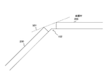
- FIG. 2 is a top view showing an example of forming the protective material 200 according to the first embodiment of the present technology.
- the corner material 102 is coated with the protective material 200, it is apt to be thin due to the surface tension, and the film thickness and shape are likely to be unstable. Further, there is a possibility that the end face becomes convex due to the influence of wet etching used when separating the substrates, and the protective material 200 becomes thinner. Therefore, in this example, the protective material 200 is formed on the linear portion 101 on the side surface of the glass substrate 100, and the corner portion 102 is not formed. That is, the protective material 200 is discontinuous at the corner portion 102. Then, without intentionally forming the protective material 200 on the corner portion 102, the corner portion 102 is protected by the protective material 200 formed on the linear portion 101. However, as will be described later, the protective material 200 may be formed on the corner portion 102 in some cases.
- a straight line 501 connecting the ridgelines of the protective material 200 formed on the straight line portion 101 of the glass substrate 100 is hypothesized.
- the ridge line is a straight line that is in contact with the peaks of the protective material 200 formed on the adjacent straight line portions 101, respectively.
- the corner portion 102 of the glass substrate 100 is inside the straight line 501 (on the center side of the glass substrate 100). Therefore, even if an impact is applied to the glass substrate 100 from a linear object, the corner portion 102 is protected from the impact.
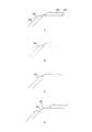
- FIG. 3 is a top view showing another example of forming the protective material 200.
- the protective material 200 in the corner portion 102 was discontinuous, but in a in the figure, the protective material 200 is also formed in the corner portion 102. Also in this case, the protective material 200 of the corner portion 102 of the glass substrate 100 is inside the straight line 501. Therefore, also in this case, even if an impact is applied to the glass substrate 100 from a linear object, the impact does not reach the protective material 200 of the corner portion 102, and the glass substrate 100 is protected from the impact.
- the protective materials 200 formed on the linear portion 101 of the glass substrate 100 are in contact with each other. Further, in c in the figure, the protective materials 200 formed on the linear portion 101 of the glass substrate 100 are closer to each other and integrated with each other. Also in these cases, even if an impact is applied to the glass substrate 100 from a linear object, the corner portion 102 is protected from the impact.
- the corner portion 102 of the glass substrate 100 is outside the straight line 501 (on the opposite side from the center of the glass substrate 100).
- the protective material 200 formed on the straight portion 101 cannot protect the corner portion 102, and the corner portion 102 is impacted. ..
- the example of forming a to c in the figure has the function of this embodiment of protecting the corner portion 102.
- the protective material 200 of the linear portion 101 is displaced due to variations in manufacturing, or the protective material 200 is applied to the corner portion 102, as long as it is an example of forming a to c in FIG. It functions as the protective material 200 of this embodiment.
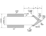
- FIG. 4 is a cross-sectional view showing an example of forming the protective material 200 on the linear portion 101 of the glass substrate 100 according to the first embodiment of the present technology.
- the wiring layer 300 is provided on at least one of the upper surface and the lower surface of the glass substrate 100 and is used as a wiring board.
- the wiring layer 300 is formed by laminating a polyimide-based insulating material and a metal conductive material. Therefore, the total thickness of the substrate when used as a wiring substrate is the thickness of the glass substrate 100 plus the thickness of the wiring layer 300.
- the thickness of the glass substrate 100 is assumed to be about 800 ⁇ m.
- the thickness of the wiring layer 300 is assumed to be about 20 to 40 ⁇ m.
- the sectional shape of the protective material 200 is a shape that bulges outward along the side surface of the glass substrate 100.
- the upper end ridge portion 104 and the lower end ridge portion 105 of the glass substrate 100 are the most widened portions. Therefore, if the protective material 200 of the upper edge portion 104 and the lower edge portion 105 is formed to be lower than the height of the wiring layer 300, there will be no practical problem as a wiring board.
- the thickness of the tip portion 203 of the protective material 200 at the tip portion 103 of the glass substrate 100 be thicker than other portions. .. This is to avoid damage at the end faces.
- a material having thixotropy is assumed as the protective material 200, it is suitable for obtaining such a shape.
- the distance from the edge of the wiring layer 300 to the upper edge portion 104 or the lower edge portion 105 of the glass substrate 100 is assumed to be, for example, about 450 to 500 ⁇ m.
- the distance (B in the figure) from the upper edge 104 or the lower edge 105 of the glass substrate 100 to the tip 103 of the glass substrate 100 is assumed to be, for example, about 200 to 250 ⁇ m.
- the thickness (C in the figure) of the tip portion 203 of the protective material 200 at the tip portion 103 of the glass substrate 100 is assumed to be, for example, about 200 ⁇ m.
- the end surface of the glass substrate 100 is projected outward, but, for example, the center portion in the thickness direction has a shape in which it enters the substrate side from both ends in the thickness direction. Good.
- the corner portion 102 of the glass substrate 100 or the protective material 200 of the corner portion 102 has the ridge lines of the protective material 200 formed on the straight portion 101 of the glass substrate 100. It is formed inside the connecting straight line 501. Accordingly, even if an impact is applied to the glass substrate 100 by a linear object, the corner portion 102 can be protected from the impact.
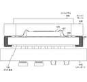
- FIG. 5 is a cross-sectional view showing an example of a semiconductor module according to the second embodiment of the present technology.
- This semiconductor module is formed including the semiconductor substrate according to the first embodiment described above. That is, the semiconductor chip 420 is mounted on the upper surface of the glass substrate 100. In this example, a semiconductor module for an image pickup device having an image pickup element (image sensor) as the semiconductor chip 420 is assumed. Each electrode of the semiconductor chip 420 is connected to the wiring layer 300 by a bonding wire 421.
- a cover glass 450 is arranged on the upper side of the glass substrate 100, that is, on the incident light side.
- a mold frame 430 is formed around the glass substrate 100 to fix the cover glass 450.
- the mold frame 430 is fixed at the corner portion 102 of the glass substrate 100 by the fixing material 440. That is, a material different from the protective material 200 is filled in the discontinuous portion of the protective material 200 in the subsequent process.
- the fixing material 440 is an example of the “material different from the protective material” in the claims.
- a solder bump or the like is provided on the lower side of the glass substrate 100 and is mounted on the motherboard 410.
- Another semiconductor chip may be mounted on the motherboard 410. In this way, the semiconductor module is formed.
- this semiconductor module is supposed to be equipped with an image pickup element as the semiconductor chip 420, it is desirable that the protective material 200 for the glass substrate 100 has a property of blocking visible light. Thereby, it is possible to avoid the influence of the external light on the glass substrate 100 on the semiconductor chip 420.
- the corner portion 102 of the glass substrate 100 on which the semiconductor chip 420 is mounted or the protective material 200 thereof is the protective material 200 formed on the straight portion 101 of the glass substrate 100. It is formed inside the straight line 501 connecting the ridge lines. Accordingly, even if a linear object impacts the glass substrate 100 of the semiconductor module, the corner portion 102 of the glass substrate 100 can be protected from the impact.
- the present technology may have the following configurations.
- the protective material is made of a material having thixotropy with a thixo ratio of 1 to 6.
- the protective material has a discontinuous portion at the corner portion, The semiconductor module according to (10), further including a material different from the protective material in the discontinuous portion.
Landscapes
- Engineering & Computer Science (AREA)
- Chemical & Material Sciences (AREA)
- Ceramic Engineering (AREA)
- Inorganic Chemistry (AREA)
- Microelectronics & Electronic Packaging (AREA)
- Chemical Kinetics & Catalysis (AREA)
- Life Sciences & Earth Sciences (AREA)
- General Chemical & Material Sciences (AREA)
- Geochemistry & Mineralogy (AREA)
- Materials Engineering (AREA)
- Organic Chemistry (AREA)
- Solid State Image Pick-Up Elements (AREA)
- Surface Treatment Of Glass (AREA)
Abstract
半導体モジュールにおけるガラス基板の側面を適切に保護する保護構造を提供する。 半導体モジュールは、ガラス基板を備える。ガラス基板は、複数の直線部と、それら直線部に挟まれたコーナー部とを側面に備える。ガラス基板の側面の少なくとも一部には、保護材が形成される。ガラス基板のコーナー部は、直線部に形成された保護材の稜線同士を結ぶ直線よりも内側(ガラス基板の中心側)にある。これにより、ガラス基板の側面に対する衝撃からコーナー部を保護する。
Description
本技術は、半導体基板に関する。詳しくは、ガラス基板を利用した半導体基板および半導体モジュールの保護構造に関する。
撮像素子の高機能化および大判化に伴い、従来のように有機基板やセラミック基板を用いて実装した場合には、反りに起因して撮像素子が浮き上がってしまったり、熱膨張率の差から接続信頼性を維持できなくなったりするおそれが生じ得る。そのため、より平坦性が担保されるガラス基板の採用が求められている。一方、ガラス基板は脆弱であり、搬送に伴う衝撃などで破損し易いため、基板外周部を樹脂などによって保護する必要がある。このガラス基板においては、特に端面が脆弱であり、例えば、端面において保護層を厚く形成するための製造方法が提案されている(例えば、特許文献1参照。)。
上述の従来技術では、耐エッチング層を設けて、耐エッチング層とガラス基板の側面とに囲まれる空間に端面保護用ポリマー剤を充填することにより、ガラス基板の側面の外側の方向に保護層を形成している。しかしながら、この従来技術では、耐エッチング層を形成した後に剥離する工程が必要になり、また、保護層が収縮することにより基板に反りが生じるおそれがある。
本技術はこのような状況に鑑みて生み出されたものであり、ガラス基板の側面を適切に保護する保護構造を提供することを目的とする。
本技術は、上述の問題点を解消するためになされたものであり、その第1の側面は、複数の直線部と上記直線部に挟まれたコーナー部とを側面に備えるガラス基板と、上記ガラス基板の側面の少なくとも一部に形成された保護材とを具備し、上記コーナー部は、上記直線部に形成された上記保護材の稜線同士を結ぶ直線よりも内側にある半導体基板および半導体モジュールである。これにより、ガラス基板の直線部に形成された保護材によってガラス基板のコーナー部を保護するという作用をもたらす。
また、この第1の側面において、上記保護材は、上記コーナー部において不連続であってもよい。すなわち、コーナー部の保護という作用をもたらすのは、直線部に形成された保護材である。
また、この第1の側面において、上記保護材は、チクソ比が1乃至6のチクソ性を有する材料からなるものであってもよい。これにより、粘性が高く外側に膨らんだ状態でガラス基板の側面に保護材を塗布するという作用をもたらす。
また、この第1の側面において、上記保護材は、リフロー工程に対する耐熱性を有する材料からなるものであってもよい。これにより、保護材を塗布した後のリフロー工程における数回に亘る高温下の処理に対応するという作用をもたらす。具体的には、耐熱温度が200度以上の材料からなるものであってもよい。
また、この第1の側面において、上記保護材は、エポキシまたはシリコーンを主成分とする材料からなるものであってもよい。
また、この第1の側面において、上記保護材は、可視光に対して遮光性を有するものであってもよい。これにより、ガラス基板に撮像素子を搭載した場合に、ガラス基板における外光による撮像素子への影響を回避するという作用をもたらす。
また、この第1の側面において、上記ガラス基板の上面および下面の少なくとも一方に積層される配線層をさらに具備してもよい。この場合、上記保護材は、上記配線層の厚みよりも厚さ方向に低く形成されることが望ましい。これにより、保護材による周囲への影響を回避するという作用をもたらす。
また、この第1の側面において、上記保護材は、上記コーナー部において不連続部を有し、上記不連続部において上記保護材とは材質の異なる材料をさらに具備してもよい。これにより、半導体モジュールにおいてガラス基板を固定する際に、コーナー部を有効に利用するという作用をもたらす。
以下、本技術を実施するための形態(以下、実施の形態と称する)について説明する。説明は以下の順序により行う。
1.第1の実施の形態(ガラス基板の側面に保護材を形成する例)
2.第2の実施の形態(半導体モジュールへの実装例)
1.第1の実施の形態(ガラス基板の側面に保護材を形成する例)
2.第2の実施の形態(半導体モジュールへの実装例)
<1.第1の実施の形態>
[半導体基板]
図1は、本技術の第1の実施の形態における半導体基板の一例を示す上面図である。
[半導体基板]
図1は、本技術の第1の実施の形態における半導体基板の一例を示す上面図である。
この半導体基板は、八角形の平面形状を有するガラス基板100を備える。すなわち、ガラス基板100は、8つの直線部101と、これら直線部101に挟まれたコーナー部102とを側面に備える。なお、この例では八角形の平面形状を示したが、これは一例であり、四角形、六角形など任意の形状であってもよい。
ガラス基板100の周囲の側面には、少なくともその一部に保護材200が形成される。この保護材200は、チクソ性(thixotropy:擬塑性)を有する材料からなる。チクソ性とは、粘度が時間経過とともに変化する性質である。チクソ性を有する材料は、力を加えると粘度が次第に低くなり、力を停止すると粘度が次第に高くなる。
この実施の形態における保護材200としては、チクソ比が1乃至6のチクソ性を有する材料からなることが望ましい。このようなチクソ性を有することにより、保護材200は、粘性が高く外側に膨らんだ状態でガラス基板100の側面に形成される。この保護材200は、ディスペンサ(液体定量吐出装置)によって、ガラス基板100に対して塗布することにより形成される。
また、ガラス基板100においては、はんだ接合を行うために、保護材200を形成した後工程として、はんだリフローが行われる。このはんだリフロー工程においては、数回に亘り高温下の処理が行われる。例えば、260度の温度が30秒間継続される。そのため、はんだリフロー工程において保護材200が収縮して、その収縮に伴う編応力によりガラス基板100が変形することを回避する必要がある。
したがって、保護材200の材料としては、はんだリフロー工程に対する耐熱性を有することが望ましい。より具体的には、保護材200の材料としては、耐熱温度(熱変形温度)が200度以上の材料からなることが望ましい。そのような材料として、例えば、エポキシ(epoxy)またはシリコーン(silicone)を主成分とする樹脂が想定される。
なお、ガラス基板100としては、ガラスを材料として用いたものの他、例えば、ガラス、絶縁材、導電材料を積層した構造であってもよい。その場合、積層されたこれらの材料が基板の端面に露出するが、その場合であっても保護材200による保護は適用可能である。
[保護材の形成]
図2は、本技術の第1の実施の形態における保護材200の形成例を示す上面図である。
図2は、本技術の第1の実施の形態における保護材200の形成例を示す上面図である。
コーナー部102は、保護材200を塗布したとしても、表面張力により薄くなり易く、また、膜厚や形状が不安定になり易い。また、基板分離の際に用いられるウエットエッチングの影響により端面が凸型になり、さらに保護材200が薄くなるおそれがある。そこで、この例では、保護材200は、ガラス基板100の側面の直線部101に形成され、コーナー部102は形成されない。すなわち、コーナー部102において保護材200は不連続となっている。そして、コーナー部102に保護材200を敢えて形成せずに、直線部101に形成された保護材200によってコーナー部102の保護を図る。ただし、後述するように、コーナー部102に保護材200が形成されていてもよい場合がある。
ここで、ガラス基板100の直線部101に形成された保護材200の稜線同士を結ぶ直線501を仮想する。稜線とは、隣り合う直線部101にそれぞれ形成された保護材200の山に対して、それぞれ接する直線である。このとき、ガラス基板100のコーナー部102は、直線501よりも内側(ガラス基板100の中心側)にある。したがって、ガラス基板100に対して直線上の物体から衝撃が加えられても、コーナー部102についてはその衝撃から保護されるようになっている。
図3は、保護材200の他の形成例を示す上面図である。
上述の例では、コーナー部102における保護材200が不連続となっていたが、同図におけるaでは、コーナー部102にも保護材200が形成されている。この場合においても、ガラス基板100のコーナー部102の保護材200は、直線501よりも内側にある。したがって、この場合も、ガラス基板100に対して直線上の物体から衝撃が加えられても、コーナー部102の保護材200にも衝撃が届かず、その衝撃から保護されるようになっている。
同図におけるbでは、ガラス基板100の直線部101に形成された保護材200同士が互いに接している。また、同図におけるcでは、ガラス基板100の直線部101に形成された保護材200同士がさらに近くなり、互いに一体化している。これらの場合においても、ガラス基板100に対して直線上の物体から衝撃が加えられても、コーナー部102についてはその衝撃から保護されるようになっている。
一方、同図におけるdの場合には、ガラス基板100のコーナー部102は、直線501よりも外側(ガラス基板100の中心から反対側)にある。この場合、ガラス基板100のコーナー部102に対して直線上の物体から衝撃が加えられると、直線部101に形成された保護材200では保護しきれずに、コーナー部102に衝撃を及ぼすことになる。
したがって、同図におけるa乃至cの形成例であれば、コーナー部102を保護するという本実施の形態としての作用を奏することがわかる。例えば、製造時のばらつきなどにより、直線部101の保護材200の位置がずれ、または、コーナー部102に保護材200が塗布されたとしても、同図におけるa乃至cの形成例であれば、この実施の形態の保護材200として機能する。
[保護材の寸法]
図4は、本技術の第1の実施の形態におけるガラス基板100の直線部101の保護材200の形成例を示す断面図である。
図4は、本技術の第1の実施の形態におけるガラス基板100の直線部101の保護材200の形成例を示す断面図である。
ガラス基板100を半導体基板として用いる際には、ガラス基板100の上面および下面の少なくとも一方に配線層300が設けられ、配線基板として利用されることになる。この配線層300は、ポリイミド系の絶縁材および金属の導電材料が積層されることにより形成される。したがって、配線基板として利用される際の基板総厚さは、ガラス基板100の厚さに配線層300の厚さを加えたものとなる。例えば、ガラス基板100の厚さとしては、800μm程度が想定される。また、配線層300の厚さとしては、20乃至40μm程度が想定される。
上述のように、保護材200としてチクソ性を有する材料を想定しているため、保護材200の断面形状は、ガラス基板100の側面に沿って外側に膨らんだ形状になる。このとき、高さ方向(厚さ方向)に着目すると、ガラス基板100の上端稜部104および下端稜部105が最も広がりのある部分である。したがって、上端稜部104および下端稜部105の保護材200が配線層300の高さよりも低く形成されていれば、配線基板としての実用上の問題は生じない。
一方、長さ方向(側面方向)に着目すると、ガラス基板100の先端部103における保護材200の先端部203の厚さ(同図におけるC)は他の部分よりも厚く形成されることが望ましい。これは、端面における破損を避けるためである。上述のように、保護材200としてチクソ性を有する材料を想定しているため、このような形状を得ることに適している。
寸法の一例として、配線層300の端からガラス基板100の上端稜部104または下端稜部105までの距離(同図におけるA)は、例えば、450乃至500μm程度が想定される。また、ガラス基板100の上端稜部104または下端稜部105からガラス基板100の先端部103までの距離(同図におけるB)は、例えば、200乃至250μm程度が想定される。また、ガラス基板100の先端部103における保護材200の先端部203の厚さ(同図におけるC)は、例えば、200μm程度が想定される。
なお、この例では、ガラス基板100の端面が外側に突出している形状を示したが、例えば、厚さ方向の中心部が厚さ方向の両端部より基板側に入り込んだ形状を有していてもよい。
このように、本技術の第1の実施の形態では、ガラス基板100のコーナー部102またはコーナー部102の保護材200が、ガラス基板100の直線部101に形成された保護材200の稜線同士を結ぶ直線501よりも内側に形成される。これにより、ガラス基板100に対して直線上の物体から衝撃が加えられても、その衝撃からコーナー部102を保護することができる。
<2.第2の実施の形態>
[半導体モジュール]
図5は、本技術の第2の実施の形態における半導体モジュールの一例を示す断面図である。
[半導体モジュール]
図5は、本技術の第2の実施の形態における半導体モジュールの一例を示す断面図である。
この半導体モジュールは、上述の第1の実施の形態における半導体基板を含んで形成される。すなわち、ガラス基板100の上面には、半導体チップ420が搭載される。この例では、半導体チップ420として撮像素子(イメージセンサ)を搭載する撮像装置のための半導体モジュールを想定する。半導体チップ420の各電極は、ボンディングワイヤ421によって配線層300に接続される。
ガラス基板100の上側、すなわち入射光側には、カバーガラス450が配置される。このカバーガラス450を固定するために、ガラス基板100の周囲にはモールドフレーム430が形成される。このモールドフレーム430は、ガラス基板100のコーナー部102において固定材440によって固定される。すなわち、上述の保護材200が不連続となっている部分に、後工程において保護材200とは異なる材料が充填される。なお、固定材440は、特許請求の範囲に記載の「保護材とは材質の異なる材料」の一例である。
ガラス基板100の下側には、はんだバンプ等が設けられ、マザーボード410に搭載される。マザーボード410にはさらに他の半導体チップが搭載され得る。このようにして、半導体モジュールが形成される。
この半導体モジュールは、半導体チップ420として撮像素子を搭載することを想定しているため、ガラス基板100の保護材200としては、可視光に対して遮光性を有することが望ましい。これにより、ガラス基板100における外光による半導体チップ420への影響を回避することができる。
このように、本技術の第2の実施の形態では、半導体チップ420を搭載するガラス基板100のコーナー部102またはその保護材200が、ガラス基板100の直線部101に形成された保護材200の稜線同士を結ぶ直線501よりも内側に形成される。これにより、半導体モジュールのガラス基板100に対して直線上の物体から衝撃が加えられても、その衝撃からガラス基板100のコーナー部102を保護することができる。
なお、上述の実施の形態は本技術を具現化するための一例を示したものであり、実施の形態における事項と、特許請求の範囲における発明特定事項とはそれぞれ対応関係を有する。同様に、特許請求の範囲における発明特定事項と、これと同一名称を付した本技術の実施の形態における事項とはそれぞれ対応関係を有する。ただし、本技術は実施の形態に限定されるものではなく、その要旨を逸脱しない範囲において実施の形態に種々の変形を施すことにより具現化することができる。
なお、本明細書に記載された効果はあくまで例示であって、限定されるものではなく、また、他の効果があってもよい。
なお、本技術は以下のような構成もとることができる。
(1)複数の直線部と前記直線部に挟まれたコーナー部とを側面に備えるガラス基板と、
前記ガラス基板の側面の少なくとも一部に形成された保護材とを具備し、
前記コーナー部は、前記直線部に形成された前記保護材の稜線同士を結ぶ直線よりも内側にある
半導体基板。
(2)前記保護材は、前記コーナー部において不連続である
前記(1)に記載の半導体基板。
(3)前記保護材は、チクソ比が1乃至6のチクソ性を有する材料からなる
前記(1)または(2)に記載の半導体基板。
(4)前記保護材は、リフロー工程に対する耐熱性を有する材料からなる
前記(1)から(3)のいずれかに記載の半導体基板。
(5)前記保護材は、耐熱温度が200度以上の材料からなる
前記(1)から(4)のいずれかに記載の半導体基板。
(6)前記保護材は、エポキシまたはシリコーンを主成分とする材料からなる
前記(1)から(5)のいずれかに記載の半導体基板。
(7)前記保護材は、可視光に対して遮光性を有する
前記(1)から(6)のいずれかに記載の半導体基板。
(8)前記ガラス基板の上面および下面の少なくとも一方に積層される配線層をさらに具備する前記(1)から(7)のいずれかに記載の半導体基板。
(9)前記保護材は、前記配線層の厚みよりも厚さ方向に低く形成される
前記(8)に記載の半導体基板。
(10)複数の直線部と前記直線部に挟まれたコーナー部とを側面に備えるガラス基板と、
前記ガラス基板の側面の少なくとも一部に形成された保護材とを具備し、
前記コーナー部は、前記直線部に形成された前記保護材の稜線同士を結ぶ直線よりも前記ガラス基板の内側にある
半導体モジュール。
(11)前記保護材は、前記コーナー部において不連続部を有し、
前記不連続部において前記保護材とは材質の異なる材料をさらに具備する
前記(10)に記載の半導体モジュール。
(1)複数の直線部と前記直線部に挟まれたコーナー部とを側面に備えるガラス基板と、
前記ガラス基板の側面の少なくとも一部に形成された保護材とを具備し、
前記コーナー部は、前記直線部に形成された前記保護材の稜線同士を結ぶ直線よりも内側にある
半導体基板。
(2)前記保護材は、前記コーナー部において不連続である
前記(1)に記載の半導体基板。
(3)前記保護材は、チクソ比が1乃至6のチクソ性を有する材料からなる
前記(1)または(2)に記載の半導体基板。
(4)前記保護材は、リフロー工程に対する耐熱性を有する材料からなる
前記(1)から(3)のいずれかに記載の半導体基板。
(5)前記保護材は、耐熱温度が200度以上の材料からなる
前記(1)から(4)のいずれかに記載の半導体基板。
(6)前記保護材は、エポキシまたはシリコーンを主成分とする材料からなる
前記(1)から(5)のいずれかに記載の半導体基板。
(7)前記保護材は、可視光に対して遮光性を有する
前記(1)から(6)のいずれかに記載の半導体基板。
(8)前記ガラス基板の上面および下面の少なくとも一方に積層される配線層をさらに具備する前記(1)から(7)のいずれかに記載の半導体基板。
(9)前記保護材は、前記配線層の厚みよりも厚さ方向に低く形成される
前記(8)に記載の半導体基板。
(10)複数の直線部と前記直線部に挟まれたコーナー部とを側面に備えるガラス基板と、
前記ガラス基板の側面の少なくとも一部に形成された保護材とを具備し、
前記コーナー部は、前記直線部に形成された前記保護材の稜線同士を結ぶ直線よりも前記ガラス基板の内側にある
半導体モジュール。
(11)前記保護材は、前記コーナー部において不連続部を有し、
前記不連続部において前記保護材とは材質の異なる材料をさらに具備する
前記(10)に記載の半導体モジュール。
100 ガラス基板
101 ガラス基板の直線部
102 ガラス基板のコーナー部
103 ガラス基板の先端部
104 ガラス基板の上端稜部
105 ガラス基板の下端稜部
200 保護材
203 保護材の先端部
300 配線層
410 マザーボード
420 半導体チップ
421 ボンディングワイヤ
430 モールドフレーム
440 固定材
450 カバーガラス
501 保護材の稜線同士を結ぶ直線
101 ガラス基板の直線部
102 ガラス基板のコーナー部
103 ガラス基板の先端部
104 ガラス基板の上端稜部
105 ガラス基板の下端稜部
200 保護材
203 保護材の先端部
300 配線層
410 マザーボード
420 半導体チップ
421 ボンディングワイヤ
430 モールドフレーム
440 固定材
450 カバーガラス
501 保護材の稜線同士を結ぶ直線
Claims (11)
- 複数の直線部と前記直線部に挟まれたコーナー部とを側面に備えるガラス基板と、
前記ガラス基板の側面の少なくとも一部に形成された保護材とを具備し、
前記コーナー部は、前記直線部に形成された前記保護材の稜線同士を結ぶ直線よりも内側にある
半導体基板。 - 前記保護材は、前記コーナー部において不連続である
請求項1記載の半導体基板。 - 前記保護材は、チクソ比が1乃至6のチクソ性を有する材料からなる
請求項1記載の半導体基板。 - 前記保護材は、リフロー工程に対する耐熱性を有する材料からなる
請求項1記載の半導体基板。 - 前記保護材は、耐熱温度が200度以上の材料からなる
請求項1記載の半導体基板。 - 前記保護材は、エポキシまたはシリコーンを主成分とする材料からなる
請求項1記載の半導体基板。 - 前記保護材は、可視光に対して遮光性を有する
請求項1記載の半導体基板。 - 前記ガラス基板の上面および下面の少なくとも一方に積層される配線層をさらに具備する請求項1記載の半導体基板。
- 前記保護材は、前記配線層の厚みよりも厚さ方向に低く形成される
請求項8記載の半導体基板。 - 複数の直線部と前記直線部に挟まれたコーナー部とを側面に備えるガラス基板と、
前記ガラス基板の側面の少なくとも一部に形成された保護材とを具備し、
前記コーナー部は、前記直線部に形成された前記保護材の稜線同士を結ぶ直線よりも前記ガラス基板の内側にある
半導体モジュール。 - 前記保護材は、前記コーナー部において不連続部を有し、
前記不連続部において前記保護材とは材質の異なる材料をさらに具備する
請求項10記載の半導体モジュール。
Priority Applications (2)
| Application Number | Priority Date | Filing Date | Title |
|---|---|---|---|
| US17/310,568 US20220102230A1 (en) | 2019-02-21 | 2019-11-25 | Semiconductor substrate and semiconductor module |
| JP2021501579A JP7441820B2 (ja) | 2019-02-21 | 2019-11-25 | 半導体基板および半導体モジュール |
Applications Claiming Priority (2)
| Application Number | Priority Date | Filing Date | Title |
|---|---|---|---|
| JP2019-029026 | 2019-02-21 | ||
| JP2019029026 | 2019-02-21 |
Publications (1)
| Publication Number | Publication Date |
|---|---|
| WO2020170535A1 true WO2020170535A1 (ja) | 2020-08-27 |
Family
ID=72144878
Family Applications (1)
| Application Number | Title | Priority Date | Filing Date |
|---|---|---|---|
| PCT/JP2019/046006 Ceased WO2020170535A1 (ja) | 2019-02-21 | 2019-11-25 | 半導体基板および半導体モジュール |
Country Status (3)
| Country | Link |
|---|---|
| US (1) | US20220102230A1 (ja) |
| JP (1) | JP7441820B2 (ja) |
| WO (1) | WO2020170535A1 (ja) |
Cited By (1)
| Publication number | Priority date | Publication date | Assignee | Title |
|---|---|---|---|---|
| EP4158686A4 (en) * | 2021-07-23 | 2024-06-19 | Absolics Inc. | Substrate comprising a lid structure, package substrate comprising the same and semiconductor device |
Families Citing this family (2)
| Publication number | Priority date | Publication date | Assignee | Title |
|---|---|---|---|---|
| KR102697845B1 (ko) * | 2023-11-02 | 2024-08-21 | 앱솔릭스 인코포레이티드 | 측면보호층을 갖는 기판 및 이의 제조방법 |
| US20250210586A1 (en) * | 2023-12-26 | 2025-06-26 | Intel Corporation | Semiconductor package substrate dicing and edge passivation |
Citations (5)
| Publication number | Priority date | Publication date | Assignee | Title |
|---|---|---|---|---|
| JP2000319040A (ja) * | 1999-05-10 | 2000-11-21 | Futou Denshi Kogyo Kk | 電子機器用ガラス板 |
| JP2005244052A (ja) * | 2004-02-27 | 2005-09-08 | New Japan Radio Co Ltd | 半導体装置の製造方法 |
| JP2013049629A (ja) * | 2012-12-10 | 2013-03-14 | Furukawa Electric Co Ltd:The | 薄板ガラスおよび薄板ガラスの製造方法 |
| JP2014502950A (ja) * | 2011-01-06 | 2014-02-06 | コーニング インコーポレイテッド | ポリマー端面保護を有する完全一体型タッチ品 |
| JP2015070047A (ja) * | 2013-09-27 | 2015-04-13 | 京セラ株式会社 | 電子部品搭載用基板および電子装置 |
Family Cites Families (4)
| Publication number | Priority date | Publication date | Assignee | Title |
|---|---|---|---|---|
| US4360820A (en) * | 1979-10-01 | 1982-11-23 | Omex | Laser recording medium |
| KR100601976B1 (ko) * | 2004-12-08 | 2006-07-18 | 삼성전자주식회사 | 스트레인 실리콘 온 인슐레이터 구조체 및 그 제조방법 |
| EP2432744B1 (en) * | 2009-05-21 | 2020-07-15 | Corning Inc. | Thin substrates having mechanically durable edges |
| JP5789889B2 (ja) * | 2014-01-10 | 2015-10-07 | 株式会社Nsc | 端面保護層付きガラス基板の製造方法 |
-
2019
- 2019-11-25 WO PCT/JP2019/046006 patent/WO2020170535A1/ja not_active Ceased
- 2019-11-25 JP JP2021501579A patent/JP7441820B2/ja active Active
- 2019-11-25 US US17/310,568 patent/US20220102230A1/en not_active Abandoned
Patent Citations (5)
| Publication number | Priority date | Publication date | Assignee | Title |
|---|---|---|---|---|
| JP2000319040A (ja) * | 1999-05-10 | 2000-11-21 | Futou Denshi Kogyo Kk | 電子機器用ガラス板 |
| JP2005244052A (ja) * | 2004-02-27 | 2005-09-08 | New Japan Radio Co Ltd | 半導体装置の製造方法 |
| JP2014502950A (ja) * | 2011-01-06 | 2014-02-06 | コーニング インコーポレイテッド | ポリマー端面保護を有する完全一体型タッチ品 |
| JP2013049629A (ja) * | 2012-12-10 | 2013-03-14 | Furukawa Electric Co Ltd:The | 薄板ガラスおよび薄板ガラスの製造方法 |
| JP2015070047A (ja) * | 2013-09-27 | 2015-04-13 | 京セラ株式会社 | 電子部品搭載用基板および電子装置 |
Cited By (1)
| Publication number | Priority date | Publication date | Assignee | Title |
|---|---|---|---|---|
| EP4158686A4 (en) * | 2021-07-23 | 2024-06-19 | Absolics Inc. | Substrate comprising a lid structure, package substrate comprising the same and semiconductor device |
Also Published As
| Publication number | Publication date |
|---|---|
| JP7441820B2 (ja) | 2024-03-01 |
| US20220102230A1 (en) | 2022-03-31 |
| JPWO2020170535A1 (ja) | 2020-08-27 |
Similar Documents
| Publication | Publication Date | Title |
|---|---|---|
| KR100793468B1 (ko) | 반도체 장치 및 그 제조 방법과, 상기 반도체 장치를 구비한 액정 모듈 및 반도체 모듈 | |
| KR102475417B1 (ko) | 댐 구조를 갖는 프리즘 시트를 포함한 반도체 패키지 | |
| JP7441820B2 (ja) | 半導体基板および半導体モジュール | |
| JP2013243340A (ja) | 電子部品、実装部材、電子機器およびこれらの製造方法 | |
| US20240055385A1 (en) | Package structure and method for fabricating the same | |
| JP2008193441A (ja) | 光学デバイス及びその製造方法 | |
| JP4197140B2 (ja) | 半導体装置 | |
| US8274125B2 (en) | Semiconductor device and semiconductor device manufacturing method | |
| CN108206195A (zh) | 半导体结构及其制作方法 | |
| US6737590B2 (en) | Tape circuit board and semiconductor chip package including the same | |
| US8026598B2 (en) | Semiconductor chip module with stacked flip-chip unit | |
| US20100181636A1 (en) | Optical device, solid-state imaging device, and method of manufacturing optical device | |
| TWI849785B (zh) | 電路裝置 | |
| JP2019046825A (ja) | 半導体装置 | |
| US20100084771A1 (en) | Flexible semiconductor package and method for fabricating the same | |
| JP7605334B2 (ja) | 気密パッケージ素子および素子モジュール | |
| US7998834B2 (en) | Substrate level bonding method and substrate level package | |
| KR100834442B1 (ko) | 증가된 결합 신뢰성을 갖는 반도체 모듈들 | |
| KR101320973B1 (ko) | 집적회로 소자 패키지 및 이의 제조 방법 | |
| TW202431577A (zh) | 電子裝置 | |
| TW202416486A (zh) | 電子裝置及其製造方法 | |
| JP2007042736A (ja) | 半導体装置及び電子モジュール、並びに、電子モジュールの製造方法 | |
| US5179435A (en) | Resin sealed semiconductor integrated circuit device | |
| KR102946108B1 (ko) | 반도체 패키지 및 그의 제조 방법 | |
| CN112038301A (zh) | 芯片、电子器件及芯片的制作方法 |
Legal Events
| Date | Code | Title | Description |
|---|---|---|---|
| 121 | Ep: the epo has been informed by wipo that ep was designated in this application |
Ref document number: 19915696 Country of ref document: EP Kind code of ref document: A1 |
|
| ENP | Entry into the national phase |
Ref document number: 2021501579 Country of ref document: JP Kind code of ref document: A |
|
| NENP | Non-entry into the national phase |
Ref country code: DE |
|
| 122 | Ep: pct application non-entry in european phase |
Ref document number: 19915696 Country of ref document: EP Kind code of ref document: A1 |