WO2020166583A1 - 大判半導体基板および割断半導体基板の製造方法 - Google Patents
大判半導体基板および割断半導体基板の製造方法 Download PDFInfo
- Publication number
- WO2020166583A1 WO2020166583A1 PCT/JP2020/005240 JP2020005240W WO2020166583A1 WO 2020166583 A1 WO2020166583 A1 WO 2020166583A1 JP 2020005240 W JP2020005240 W JP 2020005240W WO 2020166583 A1 WO2020166583 A1 WO 2020166583A1
- Authority
- WO
- WIPO (PCT)
- Prior art keywords
- semiconductor substrate
- cleaving
- main
- groove
- sized semiconductor
- Prior art date
- Legal status (The legal status is an assumption and is not a legal conclusion. Google has not performed a legal analysis and makes no representation as to the accuracy of the status listed.)
- Ceased
Links
Images





Classifications
-
- H—ELECTRICITY
- H10—SEMICONDUCTOR DEVICES; ELECTRIC SOLID-STATE DEVICES NOT OTHERWISE PROVIDED FOR
- H10F—INORGANIC SEMICONDUCTOR DEVICES SENSITIVE TO INFRARED RADIATION, LIGHT, ELECTROMAGNETIC RADIATION OF SHORTER WAVELENGTH OR CORPUSCULAR RADIATION
- H10F71/00—Manufacture or treatment of devices covered by this subclass
-
- Y—GENERAL TAGGING OF NEW TECHNOLOGICAL DEVELOPMENTS; GENERAL TAGGING OF CROSS-SECTIONAL TECHNOLOGIES SPANNING OVER SEVERAL SECTIONS OF THE IPC; TECHNICAL SUBJECTS COVERED BY FORMER USPC CROSS-REFERENCE ART COLLECTIONS [XRACs] AND DIGESTS
- Y02—TECHNOLOGIES OR APPLICATIONS FOR MITIGATION OR ADAPTATION AGAINST CLIMATE CHANGE
- Y02P—CLIMATE CHANGE MITIGATION TECHNOLOGIES IN THE PRODUCTION OR PROCESSING OF GOODS
- Y02P70/00—Climate change mitigation technologies in the production process for final industrial or consumer products
- Y02P70/50—Manufacturing or production processes characterised by the final manufactured product
Definitions
- the present invention relates to a method for manufacturing a large-sized semiconductor substrate and a cleaved semiconductor substrate.
- a square (square) shape or a semi-square (octagonal shape obtained by cutting the four corners of a quadrangle) shape is conventionally used to cut a large-sized round semiconductor wafer.
- Patent Document 1 a square (square) shape or a semi-square (octagonal shape obtained by cutting the four corners of a quadrangle) shape is conventionally used to cut a large-sized round semiconductor wafer.
- solar cells are expected to be used in various fields, and not only square-shaped or semi-square-shaped solar cells, but also various-shaped solar cells, particularly circular or elliptical solar cells. Battery cells are desired. Therefore, it is necessary to cut a square or semi-square large-sized semiconductor substrate to form a round semiconductor substrate.
- a round-shaped cleaved semiconductor obtained by cleaving a large-sized semiconductor substrate having a square shape or a semi-square shape by forming a cleaving groove (half cut) on a large-sized semiconductor substrate with a laser or a dicing saw and folding along the cleaving groove. Get the substrate.
- An object of the present invention is to provide a large-sized semiconductor substrate for obtaining a round-shaped cleaved semiconductor substrate and a method for manufacturing the round-shaped cleaved semiconductor substrate.
- the large-sized semiconductor substrate according to the present invention is a large-sized semiconductor substrate having a cleaving groove or a cleaving mark for cleaving on at least one main surface in order to obtain a cleaving semiconductor substrate by cleaving.
- a main cutting groove along a shape, at least a part of which is a closed curved main cutting groove having a circular or elliptical shape, and an auxiliary cutting groove extending from the main cutting groove toward the peripheral edge of the large-sized semiconductor substrate.
- the mark is a main cleave mark along the shape of the cleaved semiconductor substrate and has a closed curved main cleave mark having at least a part of a circular shape or an elliptical shape, and an auxiliary extending from the main cleave mark toward the peripheral edge of the large-sized semiconductor substrate. Includes fracture marks.
- a method for manufacturing a cleaved semiconductor substrate according to the present invention is a method for manufacturing a cleaved semiconductor substrate to obtain a cleaved semiconductor substrate by cleaving the large-sized semiconductor substrate, wherein in the large-sized semiconductor substrate, a main cleaving groove and an auxiliary cleaving groove are provided.
- the portion surrounded by the periphery of the large-sized semiconductor substrate is removed by folding along the main cleaving groove and the auxiliary cleaving groove, or surrounded by the main cleaving mark and the auxiliary cleaving mark and the periphery of the large-sized semiconductor substrate.
- the part is removed by folding along the main and auxiliary cleavage marks.
- a round-shaped cleaved semiconductor substrate can be obtained by cleaving a large-sized semiconductor substrate.
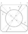
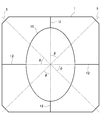
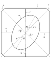
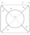
- FIG. 1 It is a figure which shows an example of the large-sized semiconductor substrate concerning this embodiment. It is a figure which shows another example of the large-sized semiconductor substrate concerning this embodiment. It is a figure which shows an example of the cleaved semiconductor substrate obtained by cleaving the large-sized semiconductor substrate shown in FIG. 1 or FIG. It is a figure which shows an example of the large-sized semiconductor substrate concerning the modification 1 of this embodiment. It is a figure which shows another example of the large-sized semiconductor substrate concerning the modification 1 of this embodiment. It is a figure which shows an example of the large-sized semiconductor substrate concerning the modification 2 of this embodiment. It is a figure which shows another example of the large-sized semiconductor substrate concerning the modification 2 of this embodiment.
- FIG. 9 is a diagram showing an example of a cleaved semiconductor substrate obtained by cleaving the large-sized semiconductor substrate of Modification 1 shown in FIG. 4 or FIG. 5 or the large-sized semiconductor substrate of Modification 2 shown in FIG. 6 or 7. It is a figure which shows an example of the large-sized semiconductor substrate which concerns on a comparative example. It is a figure which shows an example of the cleaved semiconductor substrate obtained by cleaving the large-sized semiconductor substrate of the comparative example shown in FIG.
- FIG. 1 is a diagram showing an example of a large-sized semiconductor substrate according to this embodiment
- FIG. 2 is a diagram showing another example of a large-sized semiconductor substrate according to this embodiment.
- the large-sized semiconductor substrate 1 shown in FIG. 1 or 2 is a semiconductor substrate used for, for example, a solar battery cell, and is a square-shaped or semi-square-shaped semiconductor substrate.
- the large-sized semiconductor substrate 1 has, on at least one main surface thereof, a cleaving groove or a cleaving mark (10 and 12 described later) for performing cleaving by folding.
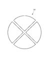
- FIG. 3 shows an example of a circular (perfect circular) cleaved semiconductor substrate 2 obtained by cleaving the large-sized semiconductor substrate 1.
- the cleaving grooves (10, 12) are formed by half-cutting with a laser or a dicing saw.
- the cleavage marks (10, 12) are laser marks formed inside the semiconductor substrate by focusing the laser inside the semiconductor substrate (so-called stealth dicing).
- stealth dicing the formation of the cleaving groove or the cleaving mark (10, 12) may be performed after stacking (forming) the layers of the solar cell, or the solar cell. It may be performed before the lamination (film formation) of the respective layers.
- a semiconductor wafer means a substrate layer such as a crystalline silicon layer, an i-type semiconductor layer, a p-type semiconductor layer, an n-type semiconductor layer, a TCO (Transparent Conductive Oxide) layer and a metal electrode.
- a substrate (wafer) on which various functional layers such as layers are formed (film formation) may be used, or a substrate layer (substrate) such as a crystalline silicon layer before these functional layers are formed (film formation). It may be a substrate consisting of only a layer).
- the cleaving grooves (10, 12) are formed up to the base material layer such as a crystalline silicon layer, and the cleaving marks (10, 12) are formed in the base material layer such as a crystalline silicon layer. Formed inside.
- Such a large-sized semiconductor substrate 1 has two cleavage directions 5 orthogonal to each other along a diagonal line due to the crystal structure (crystal orientation) of the base material layer such as a crystalline silicon layer.
- the cleaving groove includes a main cleaving groove 10 and an auxiliary cleaving groove 12.
- the cleaving trace includes the main cleaving trace 10 and the auxiliary cleaving trace 12.
- the main cleaving groove or the main cleaving trace 10 has a closed curve shape along the shape of the cleaving semiconductor substrate 2.
- the main cleaving groove or the main cleaving trace 10 has a circular shape, particularly a perfect circular closed curve shape.
- the auxiliary cleaving groove or the auxiliary cleaving mark 12 extends linearly from the main cleaving groove or the main cleaving mark 10 toward the peripheral edge of the large-sized semiconductor substrate 1.
- the closed curved main cleaving groove 10 having a circular shape (a perfect circular shape) following the shape of the cleaved semiconductor substrate 2 and the large-sized cleaving groove 10 are used. It has an auxiliary cleaving groove 12 extending toward the peripheral edge of the semiconductor substrate 1.
- the portion surrounded by the main cleaving groove 10 and the auxiliary cleaving groove 12 and the peripheral edge of the large-sized semiconductor substrate 1 is folded along the main cleaving groove 10 and the auxiliary cleaving groove 12 and removed. A round-shaped cleaved semiconductor substrate 2 is obtained.
- a closed curved main cleaving mark 10 having a circular shape (a perfect circular shape) along the shape of the cleaving semiconductor substrate 2 and the large-sized semiconductor substrate 1 from the main cleaving mark 10 are formed. It has an auxiliary fracture mark 12 extending toward the peripheral edge.
- the portion surrounded by the main cutting marks 10 and the auxiliary cutting marks 12 and the peripheral edge of the large-sized semiconductor substrate 1 is cut along the main cutting marks 10 and the auxiliary cutting marks 12 and removed.
- a round-shaped cleaved semiconductor substrate 2 is obtained.
- FIG. 9 shows an example of a large-sized semiconductor substrate of a comparative example
- FIG. 10 shows an example of a cleaved semiconductor substrate obtained by cleaving the large-sized semiconductor substrate of a comparative example.
- the auxiliary cleavage groove 12X is 0 in the cleavage direction 5X of the large-sized semiconductor substrate 1X. They differ in that they have an angle ⁇ of °.
- the large-sized semiconductor substrate 1X of the comparative example has, on one main surface thereof, a main cutting groove 10X having a circular (true circular) closed curved shape along the shape of the cutting semiconductor substrate 2X, and the large-sized semiconductor substrate 1X from the main cutting groove 10X.
- the auxiliary cutting groove 12X extends linearly toward the peripheral edge.
- the cleaving groove 10X may be cleaved along the cleavage direction 5X on the extension of the auxiliary cleaving groove 12X.
- the circular (true circular) cleaved semiconductor substrate 2 may be divided into four.
- the auxiliary cleaving groove (or auxiliary cleaving mark) 12 forms an angle ⁇ (15° or more and 45° or less) with respect to the cleavage direction 5 of the large-sized semiconductor substrate 1. Make an acute angle side.
- the portion surrounded by the main cleaving groove (or main cleaving mark) 10 and the auxiliary cleaving groove (or auxiliary cleaving mark) 12 and the peripheral edge of the large-sized semiconductor substrate 1 is divided into the main cleaving groove (or main cleaving mark) 10 and When folding along the auxiliary cleaving groove (or auxiliary cleaving mark) 12, inside the main cleaving groove (or main cleaving mark) 10, along the cleavage direction 5 on the extension of the auxiliary cleaving groove (or auxiliary cleaving mark) 12.
- auxiliary cleavage groove (or the auxiliary cleavage mark) 12 is extended and the damage is caused in the cleavage direction 5 on the extension.
- a decrease in the yield of the solar battery cell can be suppressed, and a decrease in the performance of the solar battery cell can be suppressed.
- FIG. 4 is a diagram showing an example of a large-sized semiconductor substrate according to the modified example 1 of the present embodiment
- FIG. 5 is a diagram showing another example of a large-sized semiconductor substrate according to the modified example 1 of the present embodiment
- FIG. 8 is a diagram showing an example of an elliptic cleaved semiconductor substrate 2 obtained by cleaving the large-sized semiconductor substrate of Comparative Example 1.
- the large-sized semiconductor substrate 1 of the modified example 1 shown in FIG. 4 is different from the large-sized semiconductor substrate 1 shown in FIG. 1 in that the main cleaving groove or the main cleaving mark 10 forms an elliptic closed curve.
- the large-sized semiconductor substrate 1 of the modified example 1 shown in FIG. 5 is different from the large-sized semiconductor substrate 1 shown in FIG. 2 in that the main cleaving groove or the main cleaving trace 10 forms an elliptical closed curve.
- the large-sized semiconductor substrate 1 of Modification 1 can also obtain the same advantages as the large-sized semiconductor substrate 1 of the above-described embodiment.
- FIG. 6 is a diagram showing an example of a large-sized semiconductor substrate according to Modification 2 of this embodiment
- FIG. 7 is a diagram showing another example of a large-sized semiconductor substrate according to Modification 2 of this embodiment.
- FIG. 8 is also a diagram showing an example of an elliptic cleaved semiconductor substrate 2 obtained by cleaving the large-sized semiconductor substrate of Modification 2.
- the large-sized semiconductor substrate 1 of the modified example 2 shown in FIG. The difference is that it is not located on the extension of the auxiliary cleavage mark 12.
- the major axis in the elliptical shape of the main cleaving groove or main cleaving mark 10 is auxiliary as compared with the large-sized semiconductor substrate 1 of Modification 1 shown in FIG. The difference is that it is not located on the extension of the cleaving groove or the auxiliary fracturing mark 12.
- the major axis in the elliptical shape of the main cleaving groove or main cleaving mark 10 and the auxiliary cleaving groove or auxiliary cleaving mark 12 do not have to be positioned on a straight line.
- the major-axis angle ⁇ 1 (acute angle side) in the elliptical shape of the main cleaving groove or the main cleaving mark 10 with respect to the cleavage direction 5 of the large-sized semiconductor substrate 1 is 45°
- the auxiliary for the cleavage direction 5 of the large-sized semiconductor substrate 1 is shown.
- the angle ⁇ 2 (on the acute angle side) of the cleaving groove or the auxiliary cleaving mark 12 is 15°.
- the major axis angle ⁇ 1 (acute angle side) in the elliptical shape of the main cleaving groove or main cleaving trace 10 with respect to the cleavage direction 5 of the large-sized semiconductor substrate 1 is 15°, and the cleavage direction 5 of the large-sized semiconductor substrate 1 is 5°.
- the angle ⁇ 2 (acute angle side) of the auxiliary cleaving groove or the auxiliary cleaving mark 12 with respect to is 45°.
- the large-sized semiconductor substrate 1 of Modification 2 can also obtain the same advantages as those of the large-sized semiconductor substrate 1 of the embodiment and Modification 1 described above.
- the present invention is not limited to the above-described embodiments and modifications, and various changes and modifications are possible.
- a large-sized semiconductor substrate for obtaining a circular (true circular) or elliptical cleaved semiconductor substrate has been illustrated.
- the present invention is not limited to this, and can be applied to a large-sized semiconductor substrate for obtaining a cleaved semiconductor substrate having at least a part of a circular shape (a perfect circle shape) or an elliptical shape.
- the main cleaving groove or the main cleaving trace may be a main cleaving groove or a main cleaving trace along the shape of the cleaved semiconductor substrate, and may have a closed curve shape in which at least a part is circular or elliptical.
- the large-sized semiconductor substrate in which the auxiliary cleaving groove or the auxiliary cleaving mark extends linearly has been illustrated, but the present invention is not limited to this, and the auxiliary cleaving groove or the auxiliary cleaving mark has a curved shape. It can also be applied to a large-sized semiconductor substrate extending to the.
- a large-sized semiconductor wafer including a substrate layer of a crystalline silicon layer has been illustrated.
- the present invention is not limited to this, and can be applied to a large-sized semiconductor substrate including various base material layers such as GaAs having a cleavage direction due to a crystal structure (crystal orientation).
- a large-sized semiconductor substrate for obtaining a cleaved semiconductor substrate used for a solar cell has been illustrated.
- the present invention is not limited to this, and can be applied to various large-sized semiconductor substrates for obtaining a cleaved semiconductor substrate by cleaving.
Landscapes
- Dicing (AREA)
- Mechanical Treatment Of Semiconductor (AREA)
- Photovoltaic Devices (AREA)
Abstract
ラウンド形状の割断半導体基板を得るための大判半導体基板を提供する。大判半導体基板1は、割断によって割断半導体基板を得るために、少なくとも一方主面に割断のための割断溝を有する大判半導体基板であって、割断溝は、割断半導体基板の形状に沿う主割断溝であって、少なくとも一部が円形状または楕円形状である閉曲線状の主割断溝10と、主割断溝10から大判半導体基板の周縁に向けて延びる補助割断溝12とを含む。
Description
本発明は、大判半導体基板および割断半導体基板の製造方法に関する。
例えば太陽電池セルでは、従来、ラウンド(円)形状の大判半導体基板(semiconductor wafer)をカットしたスクエア(四角)形状またはセミスクエア(四角形状の四隅をカットした八角)形状の半導体基板が用いられていた(例えば、特許文献1参照)。これにより、太陽電池モジュールにおける限られた太陽電池セル実装面積に、より多くの太陽電池セルが実装可能になり、光電変換のための受光面積が増え、太陽電池モジュールの出力が向上する。
このようなカット工程を省略するため、例えば太陽電池セルでは、近年、ラウンド形状の大判半導体基板に代えて、スクエア形状またはセミスクエア形状の大判半導体基板が用いられている。
例えば太陽電池セルは、様々な分野で利用されることが期待されており、スクエア形状またはセミスクエア形状の太陽電池セルのみならず、様々な形状の太陽電池セル、特に円形状または楕円形状の太陽電池セルが望まれている。そのため、スクエア形状またはセミスクエア形状の大判半導体基板をカットして、ラウンド形状の半導体基板を形成する必要がある。
例えば、レーザまたはダイシングソーなどにより大判半導体基板に割断溝を形成し(ハーフカット)、割断溝に沿って折り割ることにより、スクエア形状またはセミスクエア形状の大判半導体基板を割断したラウンド形状の割断半導体基板を得る。
本発明は、ラウンド形状の割断半導体基板を得るための大判半導体基板、およびラウンド形状の割断半導体基板の製造方法を提供することを目的とする。
本発明に係る大判半導体基板は、割断によって割断半導体基板を得るために、少なくとも一方主面に割断のための割断溝または割断痕を有する大判半導体基板であって、割断溝は、割断半導体基板の形状に沿う主割断溝であって、少なくとも一部が円形状または楕円形状である閉曲線状の主割断溝と、主割断溝から大判半導体基板の周縁に向けて延びる補助割断溝とを含み、割断痕は、割断半導体基板の形状に沿う主割断痕であって、少なくとも一部が円形状または楕円形状である閉曲線状の主割断痕と、主割断痕から大判半導体基板の周縁に向けて延びる補助割断痕とを含む。
本発明に係る割断半導体基板の製造方法は、上記の大判半導体基板を割断することによって割断半導体基板を得る割断半導体基板の製造方法であって、大判半導体基板において、主割断溝および補助割断溝と大判半導体基板の周縁とで囲まれた部分を、主割断溝および補助割断溝に沿って折り割ることにより除去する、または、主割断痕および補助割断痕と大判半導体基板の周縁とで囲まれた部分を、主割断痕および補助割断痕に沿って折り割ることにより除去する。
本発明によれば、大判半導体基板を割断することにより、ラウンド形状の割断半導体基板を得ることができる。
以下、添付の図面を参照して本発明の実施形態の一例について説明する。なお、各図面において同一または相当の部分に対しては同一の符号を附すこととする。また、便宜上、ハッチングや部材符号等を省略する場合もあるが、かかる場合、他の図面を参照するものとする。
図1は、本実施形態に係る大判半導体基板の一例を示す図であり、図2は、本実施形態に係る大判半導体基板の他の一例を示す図である。図1または図2に示す大判半導体基板1は、例えば太陽電池セルに用いられる半導体基板であり、スクエア形状またはセミスクエア形状の半導体基板である。大判半導体基板1は、少なくとも一方主面に、折り割りによって割断を行うための割断溝または割断痕(後述の10および12)を有する。図3に、大判半導体基板1を割断することによって得られる円形状(真円形状)の割断半導体基板2の一例を示す。
割断溝(10,12)は、レーザまたはダイシングソーなどによりハーフカットされて形成される。或いは、割断痕(10,12)は、レーザを半導体基板内部に集光することにより、半導体基板内部に形成されるレーザ痕である(所謂、ステルスダイシング)。例えば大判半導体基板1が太陽電池セルとして用いられる場合、割断溝または割断痕(10,12)の形成は、太陽電池セルの各層の積層(製膜)後に行われてもよいし、太陽電池セルの各層の積層(製膜)前に行われてもよい。
すなわち、半導体基板(semiconductor wafer)とは、結晶シリコン層等の基材層(substrate layer)に、i型半導体層、p型半導体層、n型半導体層、TCO(Transparent Conductive Oxide)層および金属電極層等の種々の機能層が形成(製膜)された基板(wafer)であってもよいし、これらの機能層が形成(製膜)される前の結晶シリコン層等の基材層(substrate layer)のみからなる基板(wafer)であってもよい。
大判半導体基板1がいずれの構成であっても、割断溝(10,12)は結晶シリコン層等の基材層まで形成され、割断痕(10,12)は結晶シリコン層等の基材層の内部に形成される。
大判半導体基板1がいずれの構成であっても、割断溝(10,12)は結晶シリコン層等の基材層まで形成され、割断痕(10,12)は結晶シリコン層等の基材層の内部に形成される。
このような大判半導体基板1は、結晶シリコン層等の基材層の結晶構造(結晶方位)に起因して、対角線に沿って直交する2つの劈開方向5を有する。
割断溝は、主割断溝10と補助割断溝12とを含む。或いは、割断痕は、主割断痕10と補助割断痕12とを含む。
主割断溝または主割断痕10は、割断半導体基板2の形状に沿う閉曲線状をなす。図1および図2では、主割断溝または主割断痕10は、円形状、特に真円形状の閉曲線状をなす。
主割断溝または主割断痕10は、割断半導体基板2の形状に沿う閉曲線状をなす。図1および図2では、主割断溝または主割断痕10は、円形状、特に真円形状の閉曲線状をなす。
補助割断溝または補助割断痕12は、主割断溝または主割断痕10から大判半導体基板1の周縁に向けて直線状に延びる。補助割断溝または補助割断痕12は、大判半導体基板1の劈開方向5に対して15°以上45°以下の角度θ(鋭角側)を有する。なお、図1ではθ=45°であり、図2ではθ=15°である。
以上説明したように、本実施形態の大判半導体基板1によれば、割断半導体基板2の形状に沿う円形状(真円形状)である閉曲線状の主割断溝10と、主割断溝10から大判半導体基板1の周縁に向けて延びる補助割断溝12とを有する。この大判半導体基板1では、主割断溝10および補助割断溝12と大判半導体基板1の周縁とで囲まれた部分を、主割断溝10および補助割断溝12に沿って折り割り、除去することにより、ラウンド形状の割断半導体基板2が得られる。或いは、本実施形態の大判半導体基板1によれば、割断半導体基板2の形状に沿う円形状(真円形状)である閉曲線状の主割断痕10と、主割断痕10から大判半導体基板1の周縁に向けて延びる補助割断痕12とを有する。この大判半導体基板1では、主割断痕10および補助割断痕12と大判半導体基板1の周縁とで囲まれた部分を、主割断痕10および補助割断痕12に沿って折り割り、除去することにより、ラウンド形状の割断半導体基板2が得られる。
ここで、図9に、比較例の大判半導体基板の一例を示し、図10に、比較例の大判半導体基板を割断することによって得られる割断半導体基板の一例を示す。図9に示す比較例の大判半導体基板1Xは、図1または図2に示す本実施形態の大判半導体基板1と比較して、補助割断溝12Xが大判半導体基板1Xの劈開方向5Xに対して0°の角度θを有する点で異なる。
比較例の大判半導体基板1Xは、一方主面に、割断半導体基板2Xの形状に沿う円形状(真円形状)の閉曲線状をなす主割断溝10Xと、主割断溝10Xから大判半導体基板1Xの周縁に向けて直線状に延びる補助割断溝12Xとを有する。
比較例の大判半導体基板1Xは、一方主面に、割断半導体基板2Xの形状に沿う円形状(真円形状)の閉曲線状をなす主割断溝10Xと、主割断溝10Xから大判半導体基板1Xの周縁に向けて直線状に延びる補助割断溝12Xとを有する。
比較例の大判半導体基板1Xでは、主割断溝10Xおよび補助割断溝12Xと大判半導体基板1Xの周縁とで囲まれた部分を、主割断溝10Xおよび補助割断溝12Xに沿って折り割る際、主割断溝10Xの内部においても、補助割断溝12Xの延長上の劈開方向5Xに沿って割断されてしまう可能性がある。これにより、図10に示すように、円形状(真円形状)の割断半導体基板2が4つに分割されてしまう可能性がある。その結果、大判半導体基板1Xを太陽電池セルとして用いる際に、太陽電池セルの歩留りが低下してしまう。
なお、主割断溝10Xの内部において、補助割断溝12Xの延長上の劈開方向5Xに沿って割断されないとしても、補助割断溝12Xの延長上の劈開方向5Xにダメージが生じる可能性がある。その結果、大判半導体基板1Xを太陽電池セルとして用いる際に、太陽電池セルの性能が低下してしまう。
これに対して、本実施形態の大判半導体基板1によれば、補助割断溝(または補助割断痕)12が、大判半導体基板1の劈開方向5に対して15°以上45°以下の角度θ(鋭角側)をなす。これにより、主割断溝(または主割断痕)10および補助割断溝(または補助割断痕)12と大判半導体基板1の周縁とで囲まれた部分を、主割断溝(または主割断痕)10および補助割断溝(または補助割断痕)12に沿って折り割る際、主割断溝(または主割断痕)10の内部において、補助割断溝(または補助割断痕)12の延長上の劈開方向5に沿って割断されること、および補助割断溝(または補助割断痕)12の延長上の劈開方向5にダメージが生じることが抑制される。その結果、大判半導体基板1を太陽電池セルとして用いる際に、太陽電池セルの歩留り低下を抑制でき、また太陽電池セルの性能低下を抑制できる。
ところで、レーザを用いたフルカットでは、割断半導体基板の端面、特に結晶シリコン層等の基材層にダメージを与えてしまうことが知られている。
これに対して、本実施形態の大判半導体基板1によれば、ハーフカット(または内部レーザ痕)と折り割りとにより、割断半導体基板2の端面、特に結晶シリコン層等の基材層に与えるダメージを抑制することができる。その結果、大判半導体基板1を太陽電池セルとして用いる際に、太陽電池セルの性能低下を抑制できる。
これに対して、本実施形態の大判半導体基板1によれば、ハーフカット(または内部レーザ痕)と折り割りとにより、割断半導体基板2の端面、特に結晶シリコン層等の基材層に与えるダメージを抑制することができる。その結果、大判半導体基板1を太陽電池セルとして用いる際に、太陽電池セルの性能低下を抑制できる。
(変形例1)
図4は、本実施形態の変形例1に係る大判半導体基板の一例を示す図であり、図5は、本実施形態の変形例1に係る大判半導体基板の他の一例を示す図である。また、図8は、比較例1の大判半導体基板を割断することによって得られる楕円形状の割断半導体基板2の一例を示す図である。
図4に示す変形例1の大判半導体基板1は、図1に示す大判半導体基板1と比較して、主割断溝または主割断痕10が楕円形状の閉曲線状をなす点で異なる。同様に、図5に示す変形例1の大判半導体基板1は、図2に示す大判半導体基板1と比較して、主割断溝または主割断痕10が楕円形状の閉曲線状をなす点で異なる。
図4は、本実施形態の変形例1に係る大判半導体基板の一例を示す図であり、図5は、本実施形態の変形例1に係る大判半導体基板の他の一例を示す図である。また、図8は、比較例1の大判半導体基板を割断することによって得られる楕円形状の割断半導体基板2の一例を示す図である。
図4に示す変形例1の大判半導体基板1は、図1に示す大判半導体基板1と比較して、主割断溝または主割断痕10が楕円形状の閉曲線状をなす点で異なる。同様に、図5に示す変形例1の大判半導体基板1は、図2に示す大判半導体基板1と比較して、主割断溝または主割断痕10が楕円形状の閉曲線状をなす点で異なる。
主割断溝または主割断痕10の楕円形状における長軸は、補助割断溝または補助割断痕12の延長上に位置する。すなわち、主割断溝または主割断痕10の楕円形状における長軸は、大判半導体基板1の劈開方向5に対して15°以上45°以下の角度θ(鋭角側)を有する。図1ではθ=45°であり、図2ではθ=15°である。
この変形例1の大判半導体基板1でも、上述した実施形態の大判半導体基板1と同様の利点を得ることができる。
(変形例2)
図6は、本実施形態の変形例2に係る大判半導体基板の一例を示す図であり、図7は、本実施形態の変形例2に係る大判半導体基板の他の一例を示す図である。また、図8は、変形例2の大判半導体基板を割断することによって得られる楕円形状の割断半導体基板2の一例をも示す図である。
図6に示す変形例2の大判半導体基板1は、図4に示す変形例1の大判半導体基板1と比較して、主割断溝または主割断痕10の楕円形状における長軸が補助割断溝または補助割断痕12の延長上に位置しない点で異なる。同様に、図7に示す変形例2の大判半導体基板1は、図5に示す変形例1の大判半導体基板1と比較して、主割断溝または主割断痕10の楕円形状における長軸が補助割断溝または補助割断痕12の延長上に位置しない点で異なる。
図6は、本実施形態の変形例2に係る大判半導体基板の一例を示す図であり、図7は、本実施形態の変形例2に係る大判半導体基板の他の一例を示す図である。また、図8は、変形例2の大判半導体基板を割断することによって得られる楕円形状の割断半導体基板2の一例をも示す図である。
図6に示す変形例2の大判半導体基板1は、図4に示す変形例1の大判半導体基板1と比較して、主割断溝または主割断痕10の楕円形状における長軸が補助割断溝または補助割断痕12の延長上に位置しない点で異なる。同様に、図7に示す変形例2の大判半導体基板1は、図5に示す変形例1の大判半導体基板1と比較して、主割断溝または主割断痕10の楕円形状における長軸が補助割断溝または補助割断痕12の延長上に位置しない点で異なる。
このように、主割断溝または主割断痕10の楕円形状における長軸と補助割断溝または補助割断痕12とは一直線上に位置していなくともよい。図6では、大判半導体基板1の劈開方向5に対する主割断溝または主割断痕10の楕円形状における長軸の角度θ1(鋭角側)は45°であり、大判半導体基板1の劈開方向5に対する補助割断溝または補助割断痕12の角度θ2(鋭角側)は15°である。一方、図7では、大判半導体基板1の劈開方向5に対する主割断溝または主割断痕10の楕円形状における長軸の角度θ1(鋭角側)は15°であり、大判半導体基板1の劈開方向5に対する補助割断溝または補助割断痕12の角度θ2(鋭角側)は45°である。
この変形例2の大判半導体基板1でも、上述した実施形態および変形例1の大判半導体基板1と同様の利点を得ることができる。
以上、本発明の実施形態および変形例について説明したが、本発明は上述した実施形態および変形例に限定されることなく、種々の変更および変形が可能である。例えば、上述した実施形態および変形例では、円形状(真円形状)または楕円形状の割断半導体基板を得るための大判半導体基板を例示した。しかし、本発明はこれに限定されず、少なくとも一部が円形状(真円形状)または楕円形状の割断半導体基板を得るための大判半導体基板にも適用可能である。この場合、主割断溝または主割断痕は、割断半導体基板の形状に沿う主割断溝または主割断痕であって、少なくとも一部が円形状または楕円形状である閉曲線状であればよい。
また、上述した実施形態および変形例では、補助割断溝または補助割断痕が直線状に延びる大判半導体基板を例示したが、本発明はこれに限定されず、補助割断溝または補助割断痕が曲線状に延びる大判半導体基板にも適用可能である。
また、上述した実施形態および変形例では、結晶シリコン層の基材層(substrate layer)を含む大判半導体基板(semiconductor wafer)を例示した。しかし、本発明はこれに限定されず、結晶構造(結晶方位)に起因する劈開方向を有するGaAs等の種々の基材層を含む大判半導体基板に適用可能である。
また、上述した実施形態および変形例では、太陽電池セルに用いられる割断半導体基板を得るための大判半導体基板を例示した。しかし、本発明はこれに限定されず、割断によって割断半導体基板を得るための種々の大判半導体基板に適用可能である。
1,1X 大判半導体基板
2,2X 割断半導体基板
5,5X 劈開方向(結晶方位)
10,10X 主割断溝または主割断痕
12,12X 補助割断溝または補助割断痕
2,2X 割断半導体基板
5,5X 劈開方向(結晶方位)
10,10X 主割断溝または主割断痕
12,12X 補助割断溝または補助割断痕
Claims (6)
- 割断によって割断半導体基板を得るために、少なくとも一方主面に前記割断のための割断溝または割断痕を有する大判半導体基板であって、
前記割断溝は、
前記割断半導体基板の形状に沿う主割断溝であって、少なくとも一部が円形状または楕円形状である閉曲線状の前記主割断溝と、
前記主割断溝から前記大判半導体基板の周縁に向けて延びる補助割断溝と、
を含み、
前記割断痕は、
前記割断半導体基板の形状に沿う主割断痕であって、少なくとも一部が円形状または楕円形状である閉曲線状の前記主割断痕と、
前記主割断痕から前記大判半導体基板の周縁に向けて延びる補助割断痕と、
を含む、
大判半導体基板。 - 前記主割断溝または前記主割断痕は真円形状である、請求項1に記載の大判半導体基板。
- 前記主割断溝または前記主割断痕は楕円形状である、請求項1に記載の大判半導体基板。
- 前記主割断溝または前記主割断痕の前記楕円形状における長軸は、前記大判半導体基板の劈開方向に対して15°以上45°以下の角度を有する、請求項3に記載の大判半導体基板。
- 前記補助割断溝または補助割断痕は、前記大判半導体基板の劈開方向に対して15°以上45°以下の角度を有する、請求項1~4のいずれか1項に記載の大判半導体基板。
- 請求項1~5のいずれか1項に記載の大判半導体基板を割断することによって割断半導体基板を得る割断半導体基板の製造方法であって、
前記大判半導体基板において、前記主割断溝および前記補助割断溝と前記大判半導体基板の周縁とで囲まれた部分を、前記主割断溝および前記補助割断溝に沿って折り割ることにより除去する、または、前記主割断痕および前記補助割断痕と前記大判半導体基板の周縁とで囲まれた部分を、前記主割断痕および前記補助割断痕に沿って折り割ることにより除去する、割断半導体基板の製造方法。
Priority Applications (1)
| Application Number | Priority Date | Filing Date | Title |
|---|---|---|---|
| JP2020572257A JP7178431B2 (ja) | 2019-02-12 | 2020-02-12 | 大判半導体基板および割断半導体基板の製造方法 |
Applications Claiming Priority (2)
| Application Number | Priority Date | Filing Date | Title |
|---|---|---|---|
| JP2019022614 | 2019-02-12 | ||
| JP2019-022614 | 2019-02-12 |
Publications (1)
| Publication Number | Publication Date |
|---|---|
| WO2020166583A1 true WO2020166583A1 (ja) | 2020-08-20 |
Family
ID=72044911
Family Applications (1)
| Application Number | Title | Priority Date | Filing Date |
|---|---|---|---|
| PCT/JP2020/005240 Ceased WO2020166583A1 (ja) | 2019-02-12 | 2020-02-12 | 大判半導体基板および割断半導体基板の製造方法 |
Country Status (2)
| Country | Link |
|---|---|
| JP (1) | JP7178431B2 (ja) |
| WO (1) | WO2020166583A1 (ja) |
Citations (2)
| Publication number | Priority date | Publication date | Assignee | Title |
|---|---|---|---|---|
| JP2010083016A (ja) * | 2008-09-30 | 2010-04-15 | Mitsuboshi Diamond Industrial Co Ltd | 脆性材料基板のスクライブ方法 |
| JP2018182078A (ja) * | 2017-04-13 | 2018-11-15 | 株式会社ディスコ | 分割方法 |
-
2020
- 2020-02-12 JP JP2020572257A patent/JP7178431B2/ja active Active
- 2020-02-12 WO PCT/JP2020/005240 patent/WO2020166583A1/ja not_active Ceased
Patent Citations (2)
| Publication number | Priority date | Publication date | Assignee | Title |
|---|---|---|---|---|
| JP2010083016A (ja) * | 2008-09-30 | 2010-04-15 | Mitsuboshi Diamond Industrial Co Ltd | 脆性材料基板のスクライブ方法 |
| JP2018182078A (ja) * | 2017-04-13 | 2018-11-15 | 株式会社ディスコ | 分割方法 |
Also Published As
| Publication number | Publication date |
|---|---|
| JPWO2020166583A1 (ja) | 2021-10-28 |
| JP7178431B2 (ja) | 2022-11-25 |
Similar Documents
| Publication | Publication Date | Title |
|---|---|---|
| JP7587624B2 (ja) | 半導体装置の製造方法 | |
| US8772137B2 (en) | Semiconductor wafer with assisting dicing structure and dicing method thereof | |
| US5182233A (en) | Compound semiconductor pellet, and method for dicing compound semiconductor wafer | |
| JP2015146446A (ja) | レーザアブレーションを利用する、太陽電池のコンタクトの形成 | |
| JP2004031526A (ja) | 3族窒化物系化合物半導体素子の製造方法 | |
| US10908022B2 (en) | Production method for fabry-perot interference filter | |
| KR20150045945A (ko) | 가공 대상물 절단 방법 | |
| KR20150044851A (ko) | 가공 대상물 절단 방법 | |
| WO2014188773A1 (ja) | 太陽電池の製造方法及び太陽電池 | |
| CN110335922A (zh) | 太阳能半片电池的切割方法 | |
| JPWO2017204326A1 (ja) | ファブリペロー干渉フィルタの製造方法 | |
| CN109920759A (zh) | 芯片的切割方法 | |
| CN107305920B (zh) | 基板晶片以及ⅲ族氮化物半导体元件的制造方法 | |
| WO2020166583A1 (ja) | 大判半導体基板および割断半導体基板の製造方法 | |
| WO2012127545A1 (ja) | 太陽電池を用いて電力を発生させる方法 | |
| CN103378211B (zh) | 太阳能电池单元及其制造方法 | |
| JP2011155057A (ja) | 半導体デバイスの製造方法および半導体基板 | |
| JP2014239085A (ja) | 太陽電池素子およびその製造方法 | |
| US11646392B2 (en) | Method of manufacturing light-emitting device | |
| JP2014239152A (ja) | 電極層を分断する溝を有する半導体素子及びその溝の形成方法 | |
| CN115939166A (zh) | 半导体装置以及其制造方法 | |
| JP7093953B2 (ja) | 半導体装置とその製造方法 | |
| US7294559B2 (en) | Wafer dicing process for optical electronic packing | |
| US20240146030A1 (en) | Semiconductor device | |
| JP3454355B2 (ja) | 窒化ガリウム系化合物半導体発光素子 |
Legal Events
| Date | Code | Title | Description |
|---|---|---|---|
| 121 | Ep: the epo has been informed by wipo that ep was designated in this application |
Ref document number: 20756174 Country of ref document: EP Kind code of ref document: A1 |
|
| ENP | Entry into the national phase |
Ref document number: 2020572257 Country of ref document: JP Kind code of ref document: A |
|
| NENP | Non-entry into the national phase |
Ref country code: DE |
|
| 122 | Ep: pct application non-entry in european phase |
Ref document number: 20756174 Country of ref document: EP Kind code of ref document: A1 |