WO2020166502A1 - 光モジュール - Google Patents
光モジュール Download PDFInfo
- Publication number
- WO2020166502A1 WO2020166502A1 PCT/JP2020/004780 JP2020004780W WO2020166502A1 WO 2020166502 A1 WO2020166502 A1 WO 2020166502A1 JP 2020004780 W JP2020004780 W JP 2020004780W WO 2020166502 A1 WO2020166502 A1 WO 2020166502A1
- Authority
- WO
- WIPO (PCT)
- Prior art keywords
- light
- optical
- optical module
- housing
- module according
- Prior art date
- Legal status (The legal status is an assumption and is not a legal conclusion. Google has not performed a legal analysis and makes no representation as to the accuracy of the status listed.)
- Ceased
Links
Images




Classifications
-
- H—ELECTRICITY
- H01—ELECTRIC ELEMENTS
- H01S—DEVICES USING THE PROCESS OF LIGHT AMPLIFICATION BY STIMULATED EMISSION OF RADIATION [LASER] TO AMPLIFY OR GENERATE LIGHT; DEVICES USING STIMULATED EMISSION OF ELECTROMAGNETIC RADIATION IN WAVE RANGES OTHER THAN OPTICAL
- H01S5/00—Semiconductor lasers
- H01S5/02—Structural details or components not essential to laser action
- H01S5/022—Mountings; Housings
- H01S5/0239—Combinations of electrical or optical elements
-
- H—ELECTRICITY
- H01—ELECTRIC ELEMENTS
- H01S—DEVICES USING THE PROCESS OF LIGHT AMPLIFICATION BY STIMULATED EMISSION OF RADIATION [LASER] TO AMPLIFY OR GENERATE LIGHT; DEVICES USING STIMULATED EMISSION OF ELECTROMAGNETIC RADIATION IN WAVE RANGES OTHER THAN OPTICAL
- H01S5/00—Semiconductor lasers
- H01S5/02—Structural details or components not essential to laser action
- H01S5/022—Mountings; Housings
- H01S5/023—Mount members, e.g. sub-mount members
- H01S5/02325—Mechanically integrated components on mount members or optical micro-benches
-
- H—ELECTRICITY
- H01—ELECTRIC ELEMENTS
- H01S—DEVICES USING THE PROCESS OF LIGHT AMPLIFICATION BY STIMULATED EMISSION OF RADIATION [LASER] TO AMPLIFY OR GENERATE LIGHT; DEVICES USING STIMULATED EMISSION OF ELECTROMAGNETIC RADIATION IN WAVE RANGES OTHER THAN OPTICAL
- H01S5/00—Semiconductor lasers
- H01S5/005—Optical components external to the laser cavity, specially adapted therefor, e.g. for homogenisation or merging of the beams or for manipulating laser pulses, e.g. pulse shaping
- H01S5/0064—Anti-reflection components, e.g. optical isolators
-
- H—ELECTRICITY
- H01—ELECTRIC ELEMENTS
- H01S—DEVICES USING THE PROCESS OF LIGHT AMPLIFICATION BY STIMULATED EMISSION OF RADIATION [LASER] TO AMPLIFY OR GENERATE LIGHT; DEVICES USING STIMULATED EMISSION OF ELECTROMAGNETIC RADIATION IN WAVE RANGES OTHER THAN OPTICAL
- H01S5/00—Semiconductor lasers
- H01S5/02—Structural details or components not essential to laser action
- H01S5/022—Mountings; Housings
- H01S5/02218—Material of the housings; Filling of the housings
-
- H—ELECTRICITY
- H01—ELECTRIC ELEMENTS
- H01S—DEVICES USING THE PROCESS OF LIGHT AMPLIFICATION BY STIMULATED EMISSION OF RADIATION [LASER] TO AMPLIFY OR GENERATE LIGHT; DEVICES USING STIMULATED EMISSION OF ELECTROMAGNETIC RADIATION IN WAVE RANGES OTHER THAN OPTICAL
- H01S5/00—Semiconductor lasers
- H01S5/02—Structural details or components not essential to laser action
- H01S5/022—Mountings; Housings
- H01S5/0225—Out-coupling of light
- H01S5/02253—Out-coupling of light using lenses
-
- H—ELECTRICITY
- H01—ELECTRIC ELEMENTS
- H01S—DEVICES USING THE PROCESS OF LIGHT AMPLIFICATION BY STIMULATED EMISSION OF RADIATION [LASER] TO AMPLIFY OR GENERATE LIGHT; DEVICES USING STIMULATED EMISSION OF ELECTROMAGNETIC RADIATION IN WAVE RANGES OTHER THAN OPTICAL
- H01S5/00—Semiconductor lasers
- H01S5/02—Structural details or components not essential to laser action
- H01S5/024—Arrangements for thermal management
- H01S5/02469—Passive cooling, e.g. where heat is removed by the housing as a whole or by a heat pipe without any active cooling element like a TEC
-
- H—ELECTRICITY
- H01—ELECTRIC ELEMENTS
- H01S—DEVICES USING THE PROCESS OF LIGHT AMPLIFICATION BY STIMULATED EMISSION OF RADIATION [LASER] TO AMPLIFY OR GENERATE LIGHT; DEVICES USING STIMULATED EMISSION OF ELECTROMAGNETIC RADIATION IN WAVE RANGES OTHER THAN OPTICAL
- H01S5/00—Semiconductor lasers
- H01S5/02—Structural details or components not essential to laser action
- H01S5/022—Mountings; Housings
- H01S5/02208—Mountings; Housings characterised by the shape of the housings
-
- H—ELECTRICITY
- H01—ELECTRIC ELEMENTS
- H01S—DEVICES USING THE PROCESS OF LIGHT AMPLIFICATION BY STIMULATED EMISSION OF RADIATION [LASER] TO AMPLIFY OR GENERATE LIGHT; DEVICES USING STIMULATED EMISSION OF ELECTROMAGNETIC RADIATION IN WAVE RANGES OTHER THAN OPTICAL
- H01S5/00—Semiconductor lasers
- H01S5/02—Structural details or components not essential to laser action
- H01S5/022—Mountings; Housings
- H01S5/0225—Out-coupling of light
- H01S5/02257—Out-coupling of light using windows, e.g. specially adapted for back-reflecting light to a detector inside the housing
-
- H—ELECTRICITY
- H01—ELECTRIC ELEMENTS
- H01S—DEVICES USING THE PROCESS OF LIGHT AMPLIFICATION BY STIMULATED EMISSION OF RADIATION [LASER] TO AMPLIFY OR GENERATE LIGHT; DEVICES USING STIMULATED EMISSION OF ELECTROMAGNETIC RADIATION IN WAVE RANGES OTHER THAN OPTICAL
- H01S5/00—Semiconductor lasers
- H01S5/02—Structural details or components not essential to laser action
- H01S5/024—Arrangements for thermal management
- H01S5/02407—Active cooling, e.g. the laser temperature is controlled by a thermo-electric cooler or water cooling
- H01S5/02415—Active cooling, e.g. the laser temperature is controlled by a thermo-electric cooler or water cooling by using a thermo-electric cooler [TEC], e.g. Peltier element
-
- H—ELECTRICITY
- H01—ELECTRIC ELEMENTS
- H01S—DEVICES USING THE PROCESS OF LIGHT AMPLIFICATION BY STIMULATED EMISSION OF RADIATION [LASER] TO AMPLIFY OR GENERATE LIGHT; DEVICES USING STIMULATED EMISSION OF ELECTROMAGNETIC RADIATION IN WAVE RANGES OTHER THAN OPTICAL
- H01S5/00—Semiconductor lasers
- H01S5/02—Structural details or components not essential to laser action
- H01S5/024—Arrangements for thermal management
- H01S5/02438—Characterized by cooling of elements other than the laser chip, e.g. an optical element being part of an external cavity or a collimating lens
-
- H—ELECTRICITY
- H01—ELECTRIC ELEMENTS
- H01S—DEVICES USING THE PROCESS OF LIGHT AMPLIFICATION BY STIMULATED EMISSION OF RADIATION [LASER] TO AMPLIFY OR GENERATE LIGHT; DEVICES USING STIMULATED EMISSION OF ELECTROMAGNETIC RADIATION IN WAVE RANGES OTHER THAN OPTICAL
- H01S5/00—Semiconductor lasers
- H01S5/10—Construction or shape of the optical resonator, e.g. extended or external cavity, coupled cavities, bent-guide, varying width, thickness or composition of the active region
- H01S5/14—External cavity lasers
- H01S5/141—External cavity lasers using a wavelength selective device, e.g. a grating or etalon
- H01S5/142—External cavity lasers using a wavelength selective device, e.g. a grating or etalon which comprises an additional resonator
Definitions
- the present invention relates to an optical module.
- an optical module a configuration is disclosed in which an optical functional element that outputs light such as a semiconductor laser element, an optical isolator and a lens that are optical components, and the like are housed in a housing (see Patent Document 1).
- the present invention has been made in view of the above, and an object thereof is to provide an optical module in which characteristic deterioration and unstable operation are suppressed.
- an optical module is an optical functional element that outputs a first light, and the first light is input, and the first light is predetermined. And the second light is input, and exerts a predetermined action on the second light to output as the third light, and at the same time, to input the second light.
- a second optical component that reflects the reflected light generated from the second light on a surface in a direction that is not coupled to the first optical component, the optical functional element, the first optical component, and the second optical component. It is characterized by comprising a housing and an optical attenuating unit which is provided inside the housing and attenuates the power of the reflected light that has been input in the housing.
- the optical module according to one aspect of the present invention is characterized in that the first optical component is a lens.
- the optical module according to one aspect of the present invention is characterized in that the second optical component is an optical isolator.
- the optical module according to one aspect of the present invention is characterized in that the housing has a height of 6.5 mm or less.
- An optical module is characterized in that the light attenuating portion is provided in a part of the housing, and the reflected light is attenuated by scattering, absorption, or transmission.
- An optical module according to an aspect of the present invention is characterized in that the light attenuating section includes a resin that scatters the reflected light.
- An optical module according to an aspect of the present invention is characterized in that the resin contains filler particles having a particle size of 0.1 ⁇ m or more and 500 ⁇ m or less.
- the optical module according to an aspect of the present invention is characterized in that the light attenuating portion is formed by subjecting a part of the housing to a surface treatment.
- the optical module according to an aspect of the present invention is characterized in that the light attenuating portion is a translucent window provided in a part of the housing.
- An optical module according to an aspect of the present invention is characterized in that an angle formed by an optical axis of the first light and an optical axis of the reflected light is 20 degrees or more.
- the distance between the position where the first optical component outputs the second light and the position where the second light is input to the input surface of the second optical component is 0. It is characterized by being 0.3 mm or more.
- the optical module according to one aspect of the present invention is characterized in that the distance between the optical axis of the second light and the optical axis of the third light is 300 ⁇ m or less.
- the optical module according to one aspect of the present invention is characterized in that the wavelength of the first light is 900 nm or more and 1650 nm or less.
- the present invention it is possible to suppress the characteristic deterioration and unstable operation of the optical module.
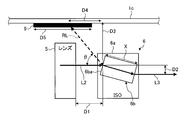
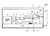
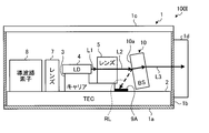
- FIG. 1 is a schematic partially cutaway side view of the optical module according to the first embodiment.
- FIG. 2 is an explanatory diagram of the configuration of FIG.
- FIG. 3 is a schematic partially cutaway side view of the optical module according to the second embodiment.
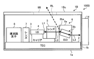
- FIG. 4 is a schematic partially cutaway side view of the optical module according to the third embodiment.
- FIG. 5 is a schematic top view of the optical module according to the fourth embodiment.
- FIG. 6 is a schematic top view of the optical module according to the fifth embodiment.
- FIG. 7 is a schematic partially cutaway side view of the optical module according to the sixth embodiment.
- FIG. 8 is a schematic top view of the optical module according to the seventh embodiment.
- FIG. 9 is a schematic top view of the optical module according to the eighth embodiment.
- FIG. 1 is a schematic partially cutaway side view of the optical module according to the first embodiment.
- FIG. 2 is an explanatory diagram of the configuration of FIG.
- FIG. 3 is a schematic partially cutaway side view of the optical module
- FIG. 10 is a schematic partially cutaway side view of the optical module according to the ninth embodiment.
- FIG. 11 is a schematic partially cutaway side view of the optical module according to the tenth embodiment.
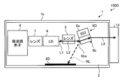
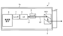
- FIG. 12 is an explanatory diagram of an example of the manufacturing process of the optical module.
- FIG. 13 is an explanatory diagram of another example of the manufacturing process of the optical module.
- FIG. 14 is an explanatory diagram of still another example of the manufacturing process of the optical module.
- FIG. 1 is a schematic partially cutaway side view of the optical module according to the first embodiment.
- the optical module 100 includes a housing 1.
- the housing 1 includes a bottom plate portion 1a, a side wall portion 1b, an upper lid portion 1c, and a light output portion 1d.
- the bottom plate portion 1a is a plate-shaped member.
- the side wall portion 1b is a frame plate-shaped member having four surfaces, and each surface is substantially orthogonal to the bottom plate portion 1a.
- the upper lid portion 1c is a plate-shaped member that is arranged to face the bottom plate portion 1a.
- the light output part 1d is a circular tubular member, and is provided on one surface of the side wall part 1b.
- a translucent window is provided in the side wall portion 1b, and light can pass from the inside of the housing 1 through the window and the light output portion 1d.
- the bottom plate portion 1a is made of a material having a high thermal conductivity such as copper tungsten (CuW), copper molybdenum (CuMo), and aluminum oxide (Al 2 O 3 ).
- the side wall portion 1b, the upper lid portion 1c, and the light output portion 1d are made of a material having a low coefficient of thermal expansion such as Fe—Ni—Co alloy and aluminum oxide (Al 2 O 3 ).
- the height of the housing 1 is defined as the height from the surface of the bottom plate portion 1a outside the housing 1 to the surface of the upper lid portion 1c outside the housing 1, the height is increased from the recent demand for downsizing of the optical module. Is preferably 6.5 mm or less.
- thermoelectric cooling element TEC
- carrier carrier
- semiconductor laser element LD
- lens optical isolator
- ISO optical isolator
- the optical module 100 is configured such that these components are mounted inside the housing 1 and the upper lid portion 1c is attached and hermetically sealed.
- the optical module 100 is configured as a semiconductor laser module. The configuration and function of each component will be described below.
- thermoelectric cooling element 2 is fixed to the bottom plate portion 1a.
- the thermoelectric cooling element 2 is externally supplied with electric power through a lead (not shown) and absorbs heat or generates heat according to the direction in which a current flows.
- the carrier 3, the semiconductor laser element 4, the lens 5, the optical isolator 6, the lens 7, and the waveguide element 8 are mounted on the thermoelectric cooling element 2. These components are controlled to the desired temperature by passing an electric current through the thermoelectric cooling element 2.
- the semiconductor laser device 4 which is an optical functional device, is mounted on the carrier 3 and is, for example, a wavelength tunable laser device.
- the carrier 3, which is also called a submount, is made of an insulating material having high thermal conductivity, and efficiently transports the heat generated by the semiconductor laser element 4 to the thermoelectric cooling element 2.
- the semiconductor laser element 4 which is an optical functional element, is supplied with power from outside via a lead (not shown) and outputs the laser light L1 as the first light to the lens 5 side.
- the wavelength of the laser light L1 is 900 nm or more and 1650 nm or less, which is suitable as a wavelength for optical communication, for example.
- the lens 5, which is the first optical component, is mounted on the carrier 3.
- the laser light L1 is input to the lens 5, and the lens 5 exerts an action due to the refractive index on the laser light L1 to collimate the laser light L1 and outputs the laser light L2 as the second light.
- the optical isolator 6, which is the second optical component, includes a magnet 6a and an optical element section 6b including a magneto-optical element and a polarizing plate.
- the laser beam L2 is input to the input surface 6ba of the optical element unit 6b, the optical isolator 6 exerts polarization and magneto-optical effects on the laser beam L2, and outputs the laser beam L3 as the third beam.
- the optical isolator 6 blocks passage of light traveling from the side of the light output unit 1d. As a result, the optical isolator 6 blocks reflected light or the like from entering the semiconductor laser element 4 from the outside.
- the optical axis of the optical element section 6b and the input surface 6ba are inclined with respect to the optical axis of the laser beam L2.
- the reflected light RL generated from the laser light L2 on the input surface 6ba travels to the upper lid portion 1c side.
- the optical isolator 6 reflects the reflected light RL in a direction not coupled to the lens 5.
- the reflected light RL is suppressed from causing characteristic deterioration and unstable operation of the semiconductor laser device 4.
- the input surface 6ba is AR-coated in order to reduce the reflectance, and the reflectance is 5% or less, preferably 2% or less.
- the angle ⁇ formed by the optical axis of the laser light L2 and the optical axis of the reflected light RL is preferably 20 degrees or more.
- the distance D1 between the position where the lens 5 outputs the laser light L2 and the position where the laser light L2 is input to the input surface 6ba is preferably 0.3 mm or more, and 0.6 mm or more. More preferable.
- the effective diameter of the optical isolator 6 is 0.5 mm when the length of the input surface 6ba of the optical element portion 6b in the tilt direction is 1.0 mm. The above can be done.
- the beam diameter LW1 of the laser beam L2 is 0.5 mm, the laser beam L2 is prevented from being eclipsed by the optical isolator 6.
- the beam diameter LW1 can be 1/e 2 full width of the beam profile of the laser beam L2.
- the angle ⁇ and the distance D1 are set so that the reflected light RL is not coupled to the lens 5 and the laser light L2 is not blocked by the optical isolator 6 according to the length of the input surface 6ba in the tilt direction.
- the angle ⁇ and the distance D1 are set so that the reflected light RL is not coupled to the lens 5 and the laser light L2 is not blocked by the optical isolator 6 according to the length of the input surface 6ba in the tilt direction.
- the angle ⁇ and the distance D1 are set so that the reflected light RL is not coupled to the lens 5 and the laser light L2 is not blocked by the optical isolator 6 according to the length of the input surface 6ba in the tilt direction.
- optical axis of the optical element portion 6b is inclined with respect to the optical axis of the laser light L2, the optical axis of the laser light L2 and the optical axis of the laser light L3 are displaced by a predetermined distance D2.
- This distance D2 is preferably 300 ⁇ m or less.
- the semiconductor laser device 4 outputs the rear-end laser light having relatively weak power from the end face (rear end face) opposite to the end face (output end face) that outputs the laser light L1 facing the lens 5. To do.
- the lens 7 collects the rear end side laser light and outputs it to the waveguide element 8.
- the waveguide element 8 is, for example, a planar lightwave circuit (PLC) element, and is provided with a ring filter whose transmission characteristics change periodically with respect to wavelength.
- the waveguide element 8 splits the rear-end side laser light into two, guides one and outputs it to a first photodetecting element (PD) (not shown), and the other transmits the ring filter to pass a ring filter (not shown). Output to 2PD.
- the current signal output from each of the first PD and the second PD is output to an external controller and used for wavelength control of the laser light L1 as in a known technique.
- An optical attenuator 9 is provided on the inside of the housing 1 of the upper lid 1c.
- the light attenuator 9 is provided at a position where the reflected light RL is input, and attenuates the power of the reflected light RL inside the housing 1.
- the reflected light RL is further reflected and input to the semiconductor laser element 4, the first PD, and the second PD, causing characteristic deterioration and unstable operation of the semiconductor laser element 4, and lowering the wavelength control accuracy of the laser light L1. It is suppressed to cause.
- the distance D3 between the position where the laser light L2 is input to the input surface 6ba and the surface of the upper lid portion 1c on the inner side of the housing 1 is determined by the magnetism of the magnet 6a of the optical isolator 6 affecting the system outside the housing 1.
- the thickness is preferably 1.0 mm or more.
- the distance D4 in the parallel direction is preferably 2.5 mm or less, for example.
- the reflected light RL irradiates the surface of the upper lid 1c on the inner side of the housing 1.
- the length of the beam diameter (length in the optical axis direction) LW2 at the time of irradiation is equal to or greater than LW2.
- the optical axis direction is the optical axis direction of the laser light L2 that is the reflected laser light.
- the length D5 is at least LW2/2 in the direction toward the semiconductor laser element 4 and the direction toward the optical isolator 6 from the position where the reflected light RL is input to the surface of the upper lid portion 1c on the inner side of the housing 1.
- the angle ⁇ is 20 degrees
- the distance D3 is 1.0 mm
- the length D5 is 1.5 mm
- the beam diameter of the reflected light RL (same as the beam diameter of the laser light L2) LW1 is 0.5 mm. It is possible to prevent the characteristics of the semiconductor laser element 4 from deteriorating, the unstable operation, and the like, and the deterioration of the wavelength control accuracy of the laser light L1 to be suppressed.
- the distance D3, the distance D4, and the angle ⁇ have the relationship of Expression (1). Further, if the beam diameter LW1 of the reflected light RL is used, the length LW2 is obtained from the angle ⁇ by the equation (2). Furthermore, the length X of the optical element portion 6b, the refractive index n of the optical element portion 6b, the angle ⁇ , and the distance D2 have the relationship of Expression (3).
- the distance D4 is 1750 ⁇ m.
- the distance D4 is 1300 ⁇ m.
- the distance D4 is 1000 ⁇ m.
- the light attenuating portion 9 can be provided at a position effective for the reflected light RL.
- the light attenuating portion 9 is formed on the surface of the upper lid portion 1c.
- the light attenuator 9 is made of resin or contains resin, and scatters the reflected light RL.
- the resin is, for example, an epoxy resin, an acrylic resin, a thermosetting polyimide, or the like, and contains filler particles having a particle diameter of 0.1 ⁇ m or more and 500 ⁇ m or less, whereby the reflected light RL can be scattered appropriately.
- the filler particles are made of a light absorbing material such as carbon black. Further, the filler particles may be made of a light scattering material such as titanium oxide (TiO 2 ), calcium carbonate (CaCO 3 ), aluminum nitride (AlN), aluminum oxide (Al 2 O 3 ).
- the light attenuating portion 9 may be formed by subjecting the surface of the upper lid portion 1c to a surface treatment.
- the light attenuating portion 9 may be configured to roughen the surface of the upper lid portion 1c to scatter the reflected light RL.
- the light attenuating portion 9 may be configured to absorb the reflected light RL by subjecting the surface of the upper lid portion 1c to surface treatment such as electroless nickel plating treatment or Raydent (registered trademark) treatment.
- the optical module 100 has suppressed characteristic deterioration and unstable operation.
- the optical functional element is not limited to the semiconductor laser element, and a semiconductor optical amplifier or a light emitting diode may be used, for example. The same applies to the following embodiments.
- FIG. 3 is a schematic partially cutaway side view of the optical module according to the second embodiment.
- This optical module 100A has a configuration in which the optical isolator 6 is replaced by the optical isolator 6A and the optical attenuator 9 is replaced by the optical attenuator 9A in the configuration of the optical module 100 according to the first embodiment.
- the other elements of the optical module 100A are the same as the corresponding elements of the optical module 100, and therefore their explanations are omitted.
- the optical isolator 6A is obtained by changing the inclination direction of the optical isolator 6 with respect to the optical axis of the optical element section 6b and the optical axis of the laser beam L2 of the input surface 6ba. As a result, the reflected light RL travels toward the thermoelectric cooling element 2 side without being coupled to the lens 5.
- the optical attenuator 9A is provided on the surface of the thermoelectric cooling element 2 on which the carrier 3 is mounted.
- the light attenuator 9A is provided at a position where the reflected light RL is input, and attenuates the power of the reflected light RL inside the housing 1.
- the light attenuating portion 9 ⁇ /b>A may be formed of resin or by subjecting the surface of the thermoelectric cooling element 2 to a surface treatment.
- the optical module 100A according to the second embodiment suppresses characteristic deterioration and unstable operation by the same action as the optical module 100.
- FIG. 4 is a schematic partially cutaway side view of the optical module according to the third embodiment.
- the optical module 100B has a configuration in which the housing 1 is replaced with the housing 1B and the light attenuating portion 9 is replaced with a light attenuating portion 9B in the configuration of the optical module 100 according to the first embodiment.
- the other elements of the optical module 100B are the same as the corresponding elements of the optical module 100, and therefore their explanations are omitted.
- the case 1B has a structure in which the upper cover 1c is replaced with an upper cover 1Bc in the structure of the case 1.
- a light attenuating portion 9B which is a translucent window, is fitted in a part of the upper lid portion 1Bc.
- the light attenuating portion 9B is made of a material that transmits the laser light L1, such as glass. It is preferable that the light attenuating portion 9A is AR-coated.
- the light attenuator 9A is provided at a position where the reflected light RL is input, and attenuates the power of the reflected light RL in the housing 1B by transmitting the reflected light RL.
- the optical module 100 ⁇ /b>B suppresses characteristic deterioration and unstable operation by the same action as the optical module 100.
- FIG. 5 is a schematic top view of the optical module according to the fourth embodiment.
- This optical module 100C has a configuration in which the optical isolator 6 is replaced by an optical isolator 6C and the optical attenuator 9 is replaced by an optical attenuator 9C in the configuration of the optical module 100 according to the first embodiment.
- the other elements of the optical module 100C are the same as the corresponding elements of the optical module 100, and thus the description thereof is omitted.
- the carrier 3 is not shown.
- FIG. 5 shows a state in which the upper lid portion 1c is removed. 6 to 9 below, the carrier 3 is not shown and the upper lid 1c is removed.
- the optical isolator 6C is obtained by changing the inclination direction of the optical isolator 6 with respect to the optical axis of the optical element section 6b and the optical axis of the laser beam L2 of the input surface 6ba. As a result, the reflected light RL travels toward the side wall portion 1b on the upper side of the drawing without being coupled to the lens 5.
- the light attenuating portion 9C is provided on the surface of the side wall portion 1b on the upper side of the drawing.
- the light attenuator 9C is provided at a position where the reflected light RL is input, and attenuates the power of the reflected light RL inside the housing 1.
- the light attenuating portion 9C may be formed of resin or by subjecting the surface of the side wall portion 1b to a surface treatment. As a result, the optical module 100C has the same function as that of the optical module 100, and thus characteristic deterioration and unstable operation are suppressed.
- FIG. 6 is a schematic top view of the optical module according to the fifth embodiment.
- This optical module 100D has a configuration in which the optical isolator 6C is replaced with an optical isolator 6D and the optical attenuating section 9C is replaced with an optical attenuating section 9D in the configuration of the optical module 100C according to the fourth embodiment.
- the other elements of the optical module 100D are the same as the corresponding elements of the optical module 100, and thus the description thereof is omitted.
- the optical isolator 6D is obtained by changing the tilt direction of the optical isolator 6 with respect to the optical axis of the optical element portion 6b and the optical axis of the laser beam L2 of the input surface 6ba. As a result, the reflected light RL travels toward the side wall 1b on the lower side of the drawing without being coupled to the lens 5.
- the light attenuating portion 9D is provided on the surface of the side wall portion 1b on the lower side of the drawing.
- the light attenuator 9D is provided at a position where the reflected light RL is input, and attenuates the power of the reflected light RL inside the housing 1.
- the light attenuating portion 9D may be formed of resin or by subjecting the surface of the side wall portion 1b to a surface treatment.
- the optical module 100D has a characteristic similar to that of the optical module 100, in which characteristic deterioration and unstable operation are suppressed.
- FIG. 7 is a schematic top view of the optical module according to the sixth embodiment.
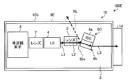
- This optical module 100E has a configuration in which the housing 1 is replaced by the housing 1E and the light attenuating portion 9C is replaced by a light attenuating portion 9E in the configuration of the optical module 100C according to the fourth embodiment.
- the other elements of the optical module 100E are the same as the corresponding elements of the optical module 100C, and thus the description thereof is omitted.
- the case 1E has a structure in which the side wall 1b is replaced with a side wall 1Eb in the structure of the case 1C.
- a light attenuating portion 9E which is a translucent window, is fitted in a part of the side wall portion 1Eb.
- the light attenuator 9E is made of a material that transmits the laser light L1, such as glass.
- the light attenuating portion 9E is preferably AR-coated.
- the light attenuator 9E is provided at a position where the reflected light RL is input, and attenuates the power of the reflected light RL in the housing 1E by transmitting the reflected light RL.
- the optical module 100E has the same function as that of the optical module 100C, and the characteristic deterioration and unstable operation are suppressed.
- FIG. 8 is a schematic top view of the optical module according to the seventh embodiment.
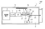
- the optical module 100F has a configuration in which the optical isolator 6C is replaced with the beam splitter 10 and the PD 11 is added in the configuration of the optical module 100C according to the fourth embodiment.
- the other elements of the optical module 100F are the same as the corresponding elements of the optical module 100, and thus the description thereof is omitted.
- the beam splitter 10 which is the second optical component, receives the laser light L2 on the input surface 10a, exerts a partial reflection action on the laser light L2, and splits the laser light L3, which is the third light, and the laser light L4. And output.
- the laser beam L4 is a part of the laser beam L2, and has a power of several% of the laser beam L2, for example.
- the input surface 10a is AR-coated to reduce the reflectance, and the reflectance is 5% or less, preferably 2% or less.
- the PD 11 is mounted on the thermoelectric cooling element 2 inside the housing 1.
- the PD 11 receives the laser beam L4 and outputs a current signal.
- the current signal is output to an external controller and used for power monitoring of the laser beam L3 as in the known technique.
- the optical axis of the beam splitter 10 and the input surface 10a are inclined with respect to the optical axis of the laser light L2.
- the reflected light RL generated from the laser light L2 on the input surface 10a travels toward the side wall portion 1b on the upper side of the drawing without being coupled to the lens 5.
- the light attenuator 9C is provided at a position where the reflected light RL is input, and attenuates the power of the reflected light RL inside the housing 1.
- the optical module 100F has a characteristic similar to that of the optical module 100C, in which characteristic deterioration and unstable operation are suppressed.
- FIG. 9 is a schematic top view of the optical module according to the eighth embodiment.
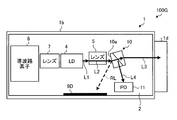
- This optical module 100G is different from the optical module 100F according to the seventh embodiment in that the optical axis of the beam splitter 10 and the inclination direction of the input surface 10a with respect to the optical axis of the laser beam L2 are changed, and the optical attenuating unit 9C is optically attenuated. It has a configuration replaced with the section 9D.
- the other elements of the optical module 100G are the same as the corresponding elements of the optical module 100F, and thus the description thereof is omitted.
- the light attenuating portion 9D is provided on the surface of the side wall portion 1b on the lower side of the drawing.
- the light attenuator 9D is provided at a position where the reflected light RL is input, and attenuates the power of the reflected light RL inside the housing 1.
- the optical module 100G suppresses characteristic deterioration and unstable operation by the same action as the optical module 100F.
- FIG. 10 is a schematic partially cutaway side view of the optical module according to the ninth embodiment.
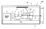
- This optical module 100H has a configuration in which the optical isolator 6 is replaced with a beam splitter 10 in the configuration of the optical module 100 according to the first embodiment, and a PD (not shown) is added.
- the other elements of the optical module 100H are the same as the corresponding elements of the optical module 100, and therefore their explanations are omitted.
- the beam splitter 10 outputs a part of the laser light L2 toward a PD (not shown).
- the optical axis of the beam splitter 10 and the input surface 10a are inclined with respect to the optical axis of the laser light L2.
- the reflected light RL generated from the laser light L2 on the input surface 10a does not couple to the lens 5 and travels toward the upper lid 1c side.
- the light attenuating portion 9 is provided on the surface of the upper lid portion 1c on the inner side of the housing 1.
- the light attenuator 9 is provided at a position where the reflected light RL is input, and attenuates the power of the reflected light RL inside the housing 1.
- the optical module 100H has the characteristics similar to those of the optical module 100, and the characteristic deterioration and the unstable operation are suppressed.
- FIG. 11 is a schematic partially cutaway side view of the optical module according to the tenth embodiment.
- This optical module 100I has a configuration in which the optical isolator 6A is replaced by the beam splitter 10 in the configuration of the optical module 100A according to the second embodiment, and a PD (not shown) is added.
- the other elements of the optical module 100I are the same as the corresponding elements of the optical module 100A, and thus the description thereof will be omitted.
- the beam splitter 10 has its optical axis and the input surface 10a inclined with respect to the optical axis of the laser beam L2 on the side opposite to that shown in FIG. Thereby, the reflected light RL generated from the laser light L2 on the input surface 10a travels to the thermoelectric cooling element 2 side without being coupled to the lens 5.
- the light attenuating portion 9A is provided on the surface of the upper lid portion 1c on the inner side of the housing 1.
- the light attenuator 9A is provided at a position where the reflected light RL is input, and attenuates the power of the reflected light RL inside the housing 1.
- the optical module 100I has a characteristic deterioration and an unstable operation suppressed by the same action as the optical module 100A.
- the reflected light RL causes deterioration of the characteristics of the semiconductor laser device 4 or failure. It is possible to suppress a stable operation and the like, and a decrease in the wavelength control accuracy of the laser light L1.
- the light attenuating portions 9A to 9E are made of, for example, resin, a material configured to absorb the reflected light RL by a surface treatment such as electroless nickel plating treatment or a raydent treatment, and a material that transmits the reflected light RL such as glass. In either case, it is preferable that the length D5 is equal to or longer than the length LW2, and the processing is easy.
- FIGS. 12 to 14 are explanatory views of an example of a manufacturing process of the optical module according to the above embodiment.
- the manufacturing processes shown in FIGS. 12 to 14 are all processes for aligning the semiconductor laser device 4.
- the optical axis conversion element OC1 is used when the semiconductor laser element 4 is arranged in the housing 1.
- the optical axis conversion element OC1 is an element that converts the position of the optical axis of the input laser beam L2 in the width direction of the housing 1 and outputs the result.
- the accuracy of the optical axis position (height direction, width direction) of the laser light L2 can be verified, and the beam quality can also be confirmed.
- the optical axis position accuracy and the beam quality of the laser light L2 can be inspected. As a result, a compact and high-quality optical module can be assembled.
- the optical axis conversion element OC2 is used when the semiconductor laser element 4 is arranged in the housing 1.
- the optical axis conversion element OC2 is an element that converts the position of the optical axis of the input laser light L2 in the height direction of the housing 1 and outputs the result.
- the optical axis conversion element OC3 is used when the semiconductor laser element 4 is arranged in the housing 1.
- the optical axis conversion element OC3 is an element that converts the position of the optical axis of the input laser light L2 in the height direction of the housing 1 and outputs the converted laser light L2. Located above the outside of 1.
- an optical axis conversion element an element that converts the position of the optical axis of the input laser and outputs it in the direction opposite to the input direction is also known.
- an optical axis conversion element even when the semiconductor laser element 4 is arranged so as to output the laser light L1 toward the side wall portion 1b opposite to the light output portion 1d, that laser light is also emitted.
- L1 can be output from the light output unit 1d to the outside of the housing 1 by an optical axis conversion element and tested.
- the present invention is not limited to the above embodiment.
- the present invention also includes those configured by appropriately combining the above-described components. Further, further effects and modified examples can be easily derived by those skilled in the art. Therefore, the broader aspects of the present invention are not limited to the above embodiments, and various modifications can be made.
- the present invention can be applied to an optical module.
- Optical output unit 2 Thermoelectric cooling element 3 Carrier 4 Semiconductor laser element 5, 7 Lens 6, 6A, 6C, 6D Optical isolator 6a Magnet 6b Optical element section 6ba, 10a Input surface 8 Waveguide element 9, 9A, 9B, 9C, 9D, 9E Optical attenuation section 10 Beam splitter 100, 100A, 100B, 100C, 100D, 100E, 100F, 100G, 100H, 100I Optical modules D1, D2 Distances L1, L2, L3, L4 Laser light OC1, OC2, OC3 Optical axis conversion element RL Reflected light ⁇ Angle
Landscapes
- Physics & Mathematics (AREA)
- Condensed Matter Physics & Semiconductors (AREA)
- General Physics & Mathematics (AREA)
- Electromagnetism (AREA)
- Optics & Photonics (AREA)
- Semiconductor Lasers (AREA)
- Optical Couplings Of Light Guides (AREA)
Abstract
光モジュールは、第1光を出力する光機能素子と、前記第1光が入力され、前記第1光に所定の作用を及ぼして第2光として出力する第1光部品と、前記第2光が入力され、前記第2光に所定の作用を及ぼして第3光として出力するとともに、前記第2光の入力面において前記第2光から発生した反射光を前記第1光部品に結合しない方向に反射させる第2光部品と、前記光機能素子、前記第1光部品、および前記第2光部品を収容する筐体と、前記筐体の内部に設けられ、入力された前記反射光の前記筐体内におけるパワーを減衰させる光減衰部と、を備える。
Description
本発明は、光モジュールに関する。
光モジュールとして、半導体レーザ素子などの光を出力する光機能素子や、光部品である光アイソレータやレンズなどが、筐体に収容された構成のものが開示されている(特許文献1参照)。
半導体レーザ素子に外部から光が入力されると、半導体レーザ素子の動作が不安定になったり、レーザ光の線幅が広くなり半導体レーザ素子の特性が劣化したりするなどの問題がある。この問題を解決するため、半導体レーザ素子が出力するレーザ光の光路上に光アイソレータを配置し、外部から半導体レーザ素子に光が入力されることを防止する構成が知られている。
しかしながら、従来の構成では、半導体レーザ素子から出力されたレーザ光の一部が光アイソレータの光入力面で反射されて半導体レーザ素子に入力し、半導体レーザ素子の特性劣化や不安定動作などの問題を引き起こす場合がある。
本発明は、上記に鑑みてなされたものであって、特性劣化や不安定動作が抑制された光モジュールを提供することを目的とする。
上述した課題を解決し、目的を達成するために、本発明の一態様に係る光モジュールは、第1光を出力する光機能素子と、前記第1光が入力され、前記第1光に所定の作用を及ぼして第2光として出力する第1光部品と、前記第2光が入力され、前記第2光に所定の作用を及ぼして第3光として出力するとともに、前記第2光の入力面において前記第2光から発生した反射光を前記第1光部品に結合しない方向に反射させる第2光部品と、前記光機能素子、前記第1光部品、および前記第2光部品を収容する筐体と、前記筐体の内部に設けられ、入力された前記反射光の前記筐体内におけるパワーを減衰させる光減衰部と、を備えることを特徴とする。
本発明の一態様に係る光モジュールは、前記第1光部品はレンズであることを特徴とする。
本発明の一態様に係る光モジュールは、前記第2光部品は光アイソレータであることを特徴とする。
本発明の一態様に係る光モジュールは、前記筐体は高さが6.5mm以下であることを特徴とする。
本発明の一態様に係る光モジュールは、前記光減衰部は、前記筐体の一部に設けられており、前記反射光は散乱または吸収または透過によって減衰されることを特徴とする。
本発明の一態様に係る光モジュールは、前記光減衰部は、前記反射光を散乱する樹脂を含むことを特徴とする。
本発明の一態様に係る光モジュールは、前記樹脂は、粒子径が0.1μm以上500μm以下のフィラー粒子を含むことを特徴とする。
本発明の一態様に係る光モジュールは、前記光減衰部は、前記筐体の一部に表面処理を行うことによって形成されているものであることを特徴とする。
本発明の一態様に係る光モジュールは、前記光減衰部は、前記筐体の一部に設けられた透光性の窓であることを特徴とする。
本発明の一態様に係る光モジュールは、前記第1光の光軸と前記反射光の光軸とが成す角度が20度以上であることを特徴とする。
本発明の一態様に係る光モジュールは、前記第1光部品が前記第2光を出力する位置と前記第2光部品の前記入力面に前記第2光が入力される位置との距離が0.3mm以上であることを特徴とする。
本発明の一態様に係る光モジュールは、前記第2光の光軸と前記第3光の光軸との距離が300μm以下であることを特徴とする。
本発明の一態様に係る光モジュールは、前記第1光の波長が900nm以上1650nm以下であることを特徴とする。
本発明によれば、光モジュールの特性劣化や不安定動作を抑制できるという効果を奏する。
(実施形態1)
図1は、実施形態1に係る光モジュールの模式的な一部切欠側面図である。この光モジュール100は、筐体1を備えている。筐体1は、底板部1aと、側壁部1bと、上蓋部1cと、光出力部1dとを備えている。底板部1aは板状の部材である。側壁部1bは、4面を有する枠板状の部材であり、各面は底板部1aと略直交している。上蓋部1cは、底板部1aと対向して配置された板状の部材である。光出力部1dは円管状の部材であり、側壁部1bの1面に設けられている。側壁部1bには透光性の窓が設けられており、筐体1内部から窓および光出力部1dを通って光が通過可能となっている。
図1は、実施形態1に係る光モジュールの模式的な一部切欠側面図である。この光モジュール100は、筐体1を備えている。筐体1は、底板部1aと、側壁部1bと、上蓋部1cと、光出力部1dとを備えている。底板部1aは板状の部材である。側壁部1bは、4面を有する枠板状の部材であり、各面は底板部1aと略直交している。上蓋部1cは、底板部1aと対向して配置された板状の部材である。光出力部1dは円管状の部材であり、側壁部1bの1面に設けられている。側壁部1bには透光性の窓が設けられており、筐体1内部から窓および光出力部1dを通って光が通過可能となっている。
底板部1aは、銅タングステン(CuW)、銅モリブデン(CuMo)、酸化アルミニウム(Al2O3)などの熱伝導率が高い材料からなる。側壁部1b、上蓋部1c、光出力部1dは、Fe-Ni-Co合金、酸化アルミニウム(Al2O3)などの熱膨張係数が低い材料からなる。なお、筐体1の高さを、底板部1aの筐体1外側の表面から上蓋部1cの筐体1外側の表面までの高さとすると、近年の光モジュールの小型化の要求から、高さは6.5mm以下が好ましい。
光モジュール100の内部には、以下のコンポーネントが収容されている:熱電冷却素子(TEC)2、キャリア3、半導体レーザ素子(LD)4、レンズ5、光アイソレータ(ISO)6、レンズ7、導波路素子8である。
光モジュール100では、筐体1の内部にこれらのコンポーネントが実装され、上蓋部1cを取り付けて気密封止されて構成されている。
光モジュール100は、半導体レーザモジュールとして構成されている。以下、各コンポーネントの構成および機能について説明する。
熱電冷却素子2は、底板部1aに固定されている。熱電冷却素子2は、外部から不図示のリードを介して電力を供給されて、電流を流す方向に応じて吸熱または発熱を行う。
キャリア3、半導体レーザ素子4、レンズ5、光アイソレータ6、レンズ7、導波路素子8は、熱電冷却素子2に搭載されている。これらのコンポーネントは、熱電冷却素子2に電流を流すことによって所望の温度に制御される。
光機能素子である半導体レーザ素子4は、キャリア3に搭載されており、たとえば波長可変レーザ素子である。キャリア3は、サブマウントとも呼ばれ、熱伝導性が高い絶縁性の材料からなり、半導体レーザ素子4が発する熱を熱電冷却素子2に効率良く輸送する。
光機能素子である半導体レーザ素子4は、外部から不図示のリードを介して電力を供給されて、第1光としてのレーザ光L1をレンズ5側に出力する。レーザ光L1の波長は、たとえば光通信の波長として好適な900nm以上1650nm以下である。
第1光部品であるレンズ5は、キャリア3に搭載されている。レンズ5は、レーザ光L1が入力され、レーザ光L1に屈折率による作用を及ぼしてコリメートし、第2光であるレーザ光L2として出力する。
第2光部品である光アイソレータ6は、磁石6aと、磁気光学素子および偏光板からなる光学素子部6bとを備えている。光アイソレータ6は、光学素子部6bの入力面6baにレーザ光L2が入力されて、レーザ光L2に偏光および磁気光学作用を及ぼし、第3光であるレーザ光L3として出力する。光アイソレータ6は、光出力部1d側から進行してきた光の通過を阻止する。これにより、光アイソレータ6は、外部から反射光などが半導体レーザ素子4に入力することを阻止する。
光学素子部6bの光軸および入力面6baは、レーザ光L2の光軸に対して傾斜している。これにより、入力面6baにおいてレーザ光L2から発生した反射光RLは、上蓋部1c側に進行する。その結果、光アイソレータ6は、反射光RLを、レンズ5に結合しない方向に反射させる。これにより、反射光RLが半導体レーザ素子4の特性劣化や不安定動作などを引き起こすことが抑制される。なお、入力面6baには反射率を低減するためにARコートが施されており、反射率は5%以下であり、好ましくは2%以下である。
反射光RLがレンズ5に結合しないようにするためには、レーザ光L2の光軸と反射光RLの光軸とが成す角度θは、20度以上であることが好ましい。また、レンズ5がレーザ光L2を出力する位置と、入力面6baにレーザ光L2が入力される位置との距離D1は、0.3mm以上であることが好ましく、0.6mm以上であることがより好ましい。角度θが20度、距離D1が0.3mmであれば、光学素子部6bの入力面6baの、傾斜方向での長さが1.0mmの場合に、光アイソレータ6の有効径を0.5mm以上とできる。これにより、レーザ光L2のビーム径LW1が0.5mmの場合には、光アイソレータ6によってレーザ光L2がけられることが防止される。ビーム径LW1は、レーザ光L2のビームプロファイルの1/e2全幅とすることができる。このように、角度θ、距離D1は、入力面6baの傾斜方向での長さに応じて、反射光RLがレンズ5に結合せず、かつ光アイソレータ6によってレーザ光L2がけられないように設定することが好ましい。
なお、光学素子部6bの光軸がレーザ光L2の光軸に対して傾斜しているので、レーザ光L2の光軸とレーザ光L3の光軸とが所定の距離D2だけずれることとなる。この距離D2は300μm以下であることが好ましい。
なお、半導体レーザ素子4は、レンズ5と対向してレーザ光L1を出力する端面(出力端面)とは反対側の端面(後端面)からも、比較的パワーが弱い後端側レーザ光を出力する。レンズ7は、後端側レーザ光を集光し、導波路素子8に出力する。
導波路素子8は、たとえば平面光波回路(PLC)素子であり、波長に対して透過特性が周期的に変化するリングフィルタを備えている。導波路素子8は、後端側レーザ光を2分割し、一方を導波して不図示の第1光検出素子(PD)に出力し、他方を、リングフィルタを透過させて不図示の第2PDに出力する。第1PDおよび第2PDのそれぞれから出力された電流信号は、外部の制御器に出力され、公知技術と同様にレーザ光L1の波長制御に使用される。
上蓋部1cの筐体1内部側には、光減衰部9が設けられている。光減衰部9は、反射光RLが入力される位置に設けられており、筐体1内における反射光RLのパワーを減衰させる。これにより、反射光RLがさらに反射して半導体レーザ素子4や第1PDや第2PDに入力され、半導体レーザ素子4の特性劣化や不安定動作などを引き起こしたり、レーザ光L1の波長制御精度の低下を引き起こしたりすることが抑制される。
図2を参照して具体的に説明する。入力面6baにレーザ光L2が入力される位置と上蓋部1cの筐体1内部側の面との距離D3は、光アイソレータ6の磁石6aによる磁性が筐体1外のシステムに影響を与えることを防ぐため、あるいは、上蓋部1cと光アイソレータ6の磁石6aが引き合い光アイソレータ6が剥離することを防ぐため等の理由から、1.0mm以上であることが好ましい。また、上蓋部1cの筐体1内部側の面に反射光RLが入力される位置と入力面6baにレーザ光L2が入力される位置との、上蓋部1cの筐体1内部側の面に平行な方向における距離D4は、例えば2.5mm以下であることが好ましい。また、上蓋部1cの筐体1内部側の面に設けられている光減衰部9の光軸方向における長さD5については、反射光RLが上蓋部1cの筐体1内部側の面に照射された時のビーム径の長さ(光軸方向における長さ)LW2以上であることが好ましい。ここで、光軸方向とは、反射されるレーザ光であるレーザ光L2の光軸方向である。この時、長さD5は、上蓋部1cの筐体1内部側の面に反射光RLが入力される位置から、半導体レーザ素子4側の方向および光アイソレータ6側の方向にそれぞれLW2/2以上であることが好ましい。また、角度θが20度、距離D3が1.0mm、長さD5が1.5mmであれば、反射光RLのビーム径(レーザ光L2のビーム径と同じ)LW1が0.5mmの場合に、半導体レーザ素子4の特性劣化や不安定動作などを引き起こしたり、レーザ光L1の波長制御精度の低下を引き起こしたりすることが抑制される。なお、距離D3、距離D4と角度θは、式(1)の関係がある。また、反射光RLのビーム径LW1を用いると、長さLW2は角度θより式(2)で求められる。さらに、光学素子部6bの長X、光学素子部6bの屈折率n、角度θと距離D2は、式(3)の関係がある。

式(1)、式(2)により、光学素子部6bの長さXが1300μm、光学素子部6bの屈折率nが2.38であるとき、以下の値になる。たとえば、角度θが30度、距離D2が200μmのとき、距離D4は1750μmである。また、角度θが38度、距離D2が250μmのとき、距離D4は1300μmである。また、角度θが45度、距離D2が300μmのとき、距離D4は1000μmである。これらのいずれの場合も、反射光RLに対して効果的な位置に光減衰部9を設けることが可能である。
光減衰部9は、上蓋部1cの表面に形成されている。光減衰部9は、樹脂からなり、または樹脂を含んで構成されており、反射光RLを散乱させる。樹脂はたとえばエポキシ樹脂、アクリル樹脂、熱硬化性ポリイミドなどであり、粒子径が0.1μm以上500μm以下のフィラー粒子を含んでおり、これにより反射光RLを好適に散乱させることができる。フィラー粒子はたとえばカーボンブラックなどの光吸収材からなる。また、フィラー粒子は、酸化チタン(TiO2)、炭酸カルシウム(CaCO3)、窒化アルミ(AlN)、酸化アルミニウム(Al2O3)などの光散乱材からなっていてもよい。また、光減衰部9は、上蓋部1cの表面に表面処理を行うことによって形成されたものでもよい。たとえば、光減衰部9は、上蓋部1cの表面に粗面処理をして反射光RLを散乱させるように構成したものでもよい。また、光減衰部9は、上蓋部1cの表面に、無電界ニッケルメッキ処理やレイデント(登録商標)処理などの表面処理をして、反射光RLを吸収するように構成したものでもよい。
以上説明した様に、実施形態1に係る光モジュール100は、特性劣化や不安定動作が抑制されたものとなる。なお、光機能素子は、半導体レーザ素子に限定されず、たとえば半導体光増幅器や発光ダイオードを用いてもよい。以降の実施形態においても同様である。
(実施形態2)
図3は、実施形態2に係る光モジュールの模式的な一部切欠側面図である。この光モジュール100Aは、実施形態1に係る光モジュール100の構成において、光アイソレータ6を光アイソレータ6Aに置き換え、光減衰部9を光減衰部9Aに置き換えた構成を有する。光モジュール100Aにおけるその他の要素については、光モジュール100における対応する要素と同様であるので、説明を省略する。
図3は、実施形態2に係る光モジュールの模式的な一部切欠側面図である。この光モジュール100Aは、実施形態1に係る光モジュール100の構成において、光アイソレータ6を光アイソレータ6Aに置き換え、光減衰部9を光減衰部9Aに置き換えた構成を有する。光モジュール100Aにおけるその他の要素については、光モジュール100における対応する要素と同様であるので、説明を省略する。
光アイソレータ6Aは、光アイソレータ6の構成において、光学素子部6bの光軸および入力面6baのレーザ光L2の光軸に対する傾斜方向を変更したものである。これにより、反射光RLはレンズ5に結合せずに熱電冷却素子2側に進行する。
光減衰部9Aは、熱電冷却素子2の、キャリア3を搭載している側の表面に設けられている。光減衰部9Aは、反射光RLが入力される位置に設けられており、筐体1内における反射光RLのパワーを減衰させる。光減衰部9Aは、光減衰部9と同様に、樹脂や、熱電冷却素子2の表面に表面処理を行うことによって形成されたものであってよい。
実施形態2に係る光モジュール100Aは、光モジュール100と同様の作用によって、特性劣化や不安定動作が抑制されたものとなる。
(実施形態3)
図4は、実施形態3に係る光モジュールの模式的な一部切欠側面図である。この光モジュール100Bは、実施形態1に係る光モジュール100の構成において、筐体1を筐体1Bに置き換え、光減衰部9を光減衰部9Bに置き換えた構成を有する。光モジュール100Bにおけるその他の要素については、光モジュール100における対応する要素と同様であるので、説明を省略する。
図4は、実施形態3に係る光モジュールの模式的な一部切欠側面図である。この光モジュール100Bは、実施形態1に係る光モジュール100の構成において、筐体1を筐体1Bに置き換え、光減衰部9を光減衰部9Bに置き換えた構成を有する。光モジュール100Bにおけるその他の要素については、光モジュール100における対応する要素と同様であるので、説明を省略する。
筐体1Bは、筐体1の構成において、上蓋部1cを上蓋部1Bcに置き換えた構成を有する。上蓋部1Bcの一部には透光性の窓である光減衰部9Bが嵌設されている。光減衰部9Bはレーザ光L1を透過する材料、たとえばガラスからなる。光減衰部9AにはARコートが施されていることが好ましい。光減衰部9Aは、反射光RLが入力される位置に設けられており、反射光RLを透過させることによって筐体1B内における反射光RLのパワーを減衰させる。これにより、光モジュール100Bは、光モジュール100と同様の作用によって、特性劣化や不安定動作が抑制されたものとなる。
(実施形態4)
図5は、実施形態4に係る光モジュールの模式的な上面図である。この光モジュール100Cは、実施形態1に係る光モジュール100の構成において、光アイソレータ6を光アイソレータ6Cに置き換え、光減衰部9を光減衰部9Cに置き換えた構成を有する。光モジュール100Cにおけるその他の要素については、光モジュール100における対応する要素と同様であるので、説明を省略する。なお、キャリア3は図示を省略している。また、説明のため、図5では上蓋部1cを取り外した状態を図示している。なお、以下の図6~図9でも、キャリア3は図示を省略し、上蓋部1cを取り外した状態を図示している。
図5は、実施形態4に係る光モジュールの模式的な上面図である。この光モジュール100Cは、実施形態1に係る光モジュール100の構成において、光アイソレータ6を光アイソレータ6Cに置き換え、光減衰部9を光減衰部9Cに置き換えた構成を有する。光モジュール100Cにおけるその他の要素については、光モジュール100における対応する要素と同様であるので、説明を省略する。なお、キャリア3は図示を省略している。また、説明のため、図5では上蓋部1cを取り外した状態を図示している。なお、以下の図6~図9でも、キャリア3は図示を省略し、上蓋部1cを取り外した状態を図示している。
光アイソレータ6Cは、光アイソレータ6の構成において、光学素子部6bの光軸および入力面6baのレーザ光L2の光軸に対する傾斜方向を変更したものである。これにより、反射光RLはレンズ5に結合せずに図面上側の側壁部1b側に進行する。
光減衰部9Cは、図面上側の側壁部1bの表面に設けられている。光減衰部9Cは、反射光RLが入力される位置に設けられており、筐体1内における反射光RLのパワーを減衰させる。光減衰部9Cは、光減衰部9と同様に、樹脂や、側壁部1bの表面に表面処理を行うことによって形成されたものであってよい。これにより、光モジュール100Cは、光モジュール100と同様の作用によって、特性劣化や不安定動作が抑制されたものとなる。
(実施形態5)
図6は、実施形態5に係る光モジュールの模式的な上面図である。この光モジュール100Dは、実施形態4に係る光モジュール100Cの構成において、光アイソレータ6Cを光アイソレータ6Dに置き換え、光減衰部9Cを光減衰部9Dに置き換えた構成を有する。光モジュール100Dにおけるその他の要素については、光モジュール100における対応する要素と同様であるので、説明を省略する。
図6は、実施形態5に係る光モジュールの模式的な上面図である。この光モジュール100Dは、実施形態4に係る光モジュール100Cの構成において、光アイソレータ6Cを光アイソレータ6Dに置き換え、光減衰部9Cを光減衰部9Dに置き換えた構成を有する。光モジュール100Dにおけるその他の要素については、光モジュール100における対応する要素と同様であるので、説明を省略する。
光アイソレータ6Dは、光アイソレータ6の構成において、光学素子部6bの光軸および入力面6baのレーザ光L2の光軸に対する傾斜方向を変更したものである。これにより、反射光RLはレンズ5に結合せずに図面下側の側壁部1b側に進行する。
光減衰部9Dは、図面下側の側壁部1bの表面に設けられている。光減衰部9Dは、反射光RLが入力される位置に設けられており、筐体1内における反射光RLのパワーを減衰させる。光減衰部9Dは、光減衰部9と同様に、樹脂や、側壁部1bの表面に表面処理を行うことによって形成されたものであってよい。これにより、光モジュール100Dは、光モジュール100と同様の作用によって、特性劣化や不安定動作が抑制されたものとなる。
(実施形態6)
図7は、実施形態6に係る光モジュールの模式的な上面図である。この光モジュール100Eは、実施形態4に係る光モジュール100Cの構成において、筐体1を筐体1Eに置き換え、光減衰部9Cを光減衰部9Eに置き換えた構成を有する。光モジュール100Eにおけるその他の要素については、光モジュール100Cにおける対応する要素と同様であるので、説明を省略する。
図7は、実施形態6に係る光モジュールの模式的な上面図である。この光モジュール100Eは、実施形態4に係る光モジュール100Cの構成において、筐体1を筐体1Eに置き換え、光減衰部9Cを光減衰部9Eに置き換えた構成を有する。光モジュール100Eにおけるその他の要素については、光モジュール100Cにおける対応する要素と同様であるので、説明を省略する。
筐体1Eは、筐体1Cの構成において、側壁部1bを側壁部1Ebに置き換えた構成を有する。側壁部1Ebの一部には透光性の窓である光減衰部9Eが嵌設されている。光減衰部9Eはレーザ光L1を透過する材料、たとえばガラスからなる。光減衰部9EにはARコートが施されていることが好ましい。光減衰部9Eは、反射光RLが入力される位置に設けられており、反射光RLを透過させることによって筐体1E内における反射光RLのパワーを減衰させる。これにより、光モジュール100Eは、光モジュール100Cと同様の作用によって、特性劣化や不安定動作が抑制されたものとなる。
(実施形態7)
図8は、実施形態7に係る光モジュールの模式的な上面図である。この光モジュール100Fは、実施形態4に係る光モジュール100Cの構成において、光アイソレータ6Cをビームスプリッタ10に置き換え、PD11を追加した構成を有する。光モジュール100Fにおけるその他の要素については、光モジュール100における対応する要素と同様であるので、説明を省略する。
図8は、実施形態7に係る光モジュールの模式的な上面図である。この光モジュール100Fは、実施形態4に係る光モジュール100Cの構成において、光アイソレータ6Cをビームスプリッタ10に置き換え、PD11を追加した構成を有する。光モジュール100Fにおけるその他の要素については、光モジュール100における対応する要素と同様であるので、説明を省略する。
第2光部品であるビームスプリッタ10は、入力面10aにレーザ光L2が入力されて、レーザ光L2に部分的反射作用を及ぼし、第3光であるレーザ光L3と、レーザ光L4とに分岐して出力する。レーザ光L4はレーザ光L2の一部であり、たとえばレーザ光L2の数%のパワーである。なお、入力面10aには反射率を低減するためにARコートが施されており、反射率は5%以下であり、好ましくは2%以下である。
PD11は、筐体1内で熱電冷却素子2に搭載されている。PD11は、レーザ光L4を受光し、電流信号を出力する。電流信号は、外部の制御器に出力され、公知技術と同様にレーザ光L3のパワーモニタに使用される。
ビームスプリッタ10の光軸および入力面10aは、レーザ光L2の光軸に対して傾斜している。これにより、入力面10aにおいてレーザ光L2から発生した反射光RLは、レンズ5に結合せずに図面上側の側壁部1b側に進行する。光減衰部9Cは、反射光RLが入力される位置に設けられており、筐体1内における反射光RLのパワーを減衰させる。これにより、光モジュール100Fは、光モジュール100Cと同様の作用によって、特性劣化や不安定動作が抑制されたものとなる。
(実施形態8)
図9は、実施形態8に係る光モジュールの模式的な上面図である。この光モジュール100Gは、実施形態7に係る光モジュール100Fの構成において、ビームスプリッタ10の光軸および入力面10aのレーザ光L2の光軸に対する傾斜方向を変更し、かつ光減衰部9Cを光減衰部9Dに置き換えた構成を有する。光モジュール100Gにおけるその他の要素については、光モジュール100Fにおける対応する要素と同様であるので、説明を省略する。
図9は、実施形態8に係る光モジュールの模式的な上面図である。この光モジュール100Gは、実施形態7に係る光モジュール100Fの構成において、ビームスプリッタ10の光軸および入力面10aのレーザ光L2の光軸に対する傾斜方向を変更し、かつ光減衰部9Cを光減衰部9Dに置き換えた構成を有する。光モジュール100Gにおけるその他の要素については、光モジュール100Fにおける対応する要素と同様であるので、説明を省略する。
光減衰部9Dは、図面下側の側壁部1bの表面に設けられている。光減衰部9Dは、反射光RLが入力される位置に設けられており、筐体1内における反射光RLのパワーを減衰させる。これにより、光モジュール100Gは、光モジュール100Fと同様の作用によって、特性劣化や不安定動作が抑制されたものとなる。
(実施形態9)
図10は、実施形態9に係る光モジュールの模式的な一部切欠側面図である。この光モジュール100Hは、実施形態1に係る光モジュール100の構成において、光アイソレータ6をビームスプリッタ10に置き換え、不図示のPDを追加した構成を有する。光モジュール100Hにおけるその他の要素については、光モジュール100における対応する要素と同様であるので、説明を省略する。
図10は、実施形態9に係る光モジュールの模式的な一部切欠側面図である。この光モジュール100Hは、実施形態1に係る光モジュール100の構成において、光アイソレータ6をビームスプリッタ10に置き換え、不図示のPDを追加した構成を有する。光モジュール100Hにおけるその他の要素については、光モジュール100における対応する要素と同様であるので、説明を省略する。
ビームスプリッタ10は、レーザ光L2の一部を不図示のPDに向けて出力する。ビームスプリッタ10は、その光軸および入力面10aが、レーザ光L2の光軸に対して傾斜している。これにより、入力面10aにおいてレーザ光L2から発生した反射光RLは、レンズ5に結合せず、上蓋部1c側に進行する。光減衰部9は、上蓋部1cにおける筐体1の内部側の表面に設けられている。光減衰部9は、反射光RLが入力される位置に設けられており、筐体1内における反射光RLのパワーを減衰させる。これにより、光モジュール100Hは、光モジュール100と同様の作用によって、特性劣化や不安定動作が抑制されたものとなる。
(実施形態10)
図11は、実施形態10に係る光モジュールの模式的な一部切欠側面図である。この光モジュール100Iは、実施形態2に係る光モジュール100Aの構成において、光アイソレータ6Aをビームスプリッタ10に置き換え、不図示のPDを追加した構成を有する。光モジュール100Iにおけるその他の要素については、光モジュール100Aにおける対応する要素と同様であるので、説明を省略する。
図11は、実施形態10に係る光モジュールの模式的な一部切欠側面図である。この光モジュール100Iは、実施形態2に係る光モジュール100Aの構成において、光アイソレータ6Aをビームスプリッタ10に置き換え、不図示のPDを追加した構成を有する。光モジュール100Iにおけるその他の要素については、光モジュール100Aにおける対応する要素と同様であるので、説明を省略する。
ビームスプリッタ10は、その光軸および入力面10aが、レーザ光L2の光軸に対して、図10に示す場合とは反対側に傾斜している。これにより、入力面10aにおいてレーザ光L2から発生した反射光RLは、レンズ5に結合せずに熱電冷却素子2側に進行する。光減衰部9Aは、上蓋部1cにおける筐体1の内部側の表面に設けられている。光減衰部9Aは、反射光RLが入力される位置に設けられており、筐体1内における反射光RLのパワーを減衰させる。これにより、光モジュール100Iは、光モジュール100Aと同様の作用によって、特性劣化や不安定動作が抑制されたものとなる。
光減衰部9A~9Eについても、長さD5(図2における光減衰部9の長さD5に相当)が長さLW2以上であれば、反射光RLが、半導体レーザ素子4の特性劣化や不安定動作などを引き起こしたり、レーザ光L1の波長制御精度の低下を引き起こしたりすることを抑制することができる。光減衰部9A~9Eは、たとえば、樹脂、無電界ニッケルメッキ処理やレイデント処理などの表面処理により反射光RLを吸収するように構成したもの、および反射光RLを透過する材料たとえばガラスからなるもののいずれかであるが、いずれの場合でも、長さD5が長さLW2以上であることが好ましく、加工が容易である。
(組み立て方法)
図12、13、14は、上記実施形態に係る光モジュールの製造工程の一例の説明図である。図12~14に示す製造工程は、いずれも半導体レーザ素子4の位置合わせを行うための工程である。
図12、13、14は、上記実施形態に係る光モジュールの製造工程の一例の説明図である。図12~14に示す製造工程は、いずれも半導体レーザ素子4の位置合わせを行うための工程である。
図12に示す例では、筐体1内に半導体レーザ素子4を配置する際に、光軸変換素子OC1を利用する。光軸変換素子OC1は、入力されたレーザ光L2の光軸の位置を、筐体1の幅方向で変換して出力する素子である。このような素子を用いることで、レーザ光L2の光軸位置(高さ方向、幅方向)の精度を検証でき、ビーム品質も確認可能である。具体的には、レーザ光L2を光出力部1dから筐体1の外部に出力させて機器等で観測することによって、レーザ光L2の光軸位置精度やビーム品質を検査できる。これにより、小型かつ高品質な光モジュールの組み立てを実現できる。
図13に示す例では、筐体1内に半導体レーザ素子4を配置する際に、光軸変換素子OC2を利用する。光軸変換素子OC2は、入力されたレーザ光L2の光軸の位置を、筐体1の高さ方向で変換して出力する素子である。レーザ光L2を光出力部1dから筐体1の外部に出力させて機器等で観測することによって、レーザ光L2の光軸位置精度やビーム品質を検査できる。これにより、小型かつ高品質な光モジュールの組み立てを実現できる。
図14に示す例では、筐体1内に半導体レーザ素子4を配置する際に、光軸変換素子OC3を利用する。光軸変換素子OC3は、入力されたレーザ光L2の光軸の位置を、筐体1の高さ方向で変換して出力する素子であるが、変換されたレーザ光L2の光軸は筐体1の外部の上方に位置する。このようにしてレーザ光L2を筐体1の外部に出力させて機器等で観測することによって、レーザ光L2の光軸位置精度やビーム品質を検査できる。これにより、小型かつ高品質な光モジュールの組み立てを実現できる。
なお、光軸変換素子として、入力されたレーザの光軸の位置を変換し、入力された方向とは反対の方向に出力する素子も公知である。このような光軸変換素子を利用すれば、半導体レーザ素子4が光出力部1dとは反対側の側壁部1bに向けてレーザ光L1を出力するように配置される場合にも、そのレーザ光L1を光軸変換素子によって光出力部1dから筐体1の外部に出力させ、検査することができる。
また、上記実施形態により本発明が限定されるものではない。上述した各構成要素を適宜組み合わせて構成したものも本発明に含まれる。また、さらなる効果や変形例は、当業者によって容易に導き出すことができる。よって、本発明のより広範な態様は、上記の実施形態に限定されるものではなく、様々な変更が可能である。
本発明は、光モジュールに利用することができる。
1、1B、1C、1E 筐体
1a 底板部
1b、1Eb 側壁部
1c、1Bc 上蓋部
1d 光出力部
2 熱電冷却素子
3 キャリア
4 半導体レーザ素子
5、7 レンズ
6、6A、6C、6D 光アイソレータ
6a 磁石
6b 光学素子部
6ba、10a 入力面
8 導波路素子
9、9A、9B、9C、9D、9E 光減衰部
10 ビームスプリッタ
100、100A、100B、100C、100D、100E、100F、100G、100H、100I 光モジュール
D1、D2 距離
L1、L2、L3、L4 レーザ光
OC1、OC2、OC3 光軸変換素子
RL 反射光
θ 角度
1a 底板部
1b、1Eb 側壁部
1c、1Bc 上蓋部
1d 光出力部
2 熱電冷却素子
3 キャリア
4 半導体レーザ素子
5、7 レンズ
6、6A、6C、6D 光アイソレータ
6a 磁石
6b 光学素子部
6ba、10a 入力面
8 導波路素子
9、9A、9B、9C、9D、9E 光減衰部
10 ビームスプリッタ
100、100A、100B、100C、100D、100E、100F、100G、100H、100I 光モジュール
D1、D2 距離
L1、L2、L3、L4 レーザ光
OC1、OC2、OC3 光軸変換素子
RL 反射光
θ 角度
Claims (13)
- 第1光を出力する光機能素子と、
前記第1光が入力され、前記第1光に所定の作用を及ぼして第2光として出力する第1光部品と、
前記第2光が入力され、前記第2光に所定の作用を及ぼして第3光として出力するとともに、前記第2光の入力面において前記第2光から発生した反射光を前記第1光部品に結合しない方向に反射させる第2光部品と、
前記光機能素子、前記第1光部品、および前記第2光部品を収容する筐体と、
前記筐体の内部に設けられ、入力された前記反射光の前記筐体内におけるパワーを減衰させる光減衰部と、
を備えることを特徴とする光モジュール。 - 前記第1光部品はレンズであることを特徴とする請求項1に記載の光モジュール。
- 前記第2光部品は光アイソレータであることを特徴とする請求項1または2に記載の光モジュール。
- 前記筐体は高さが6.5mm以下であることを特徴とする請求項1~3のいずれか一つに記載の光モジュール。
- 前記光減衰部は、前記筐体の一部に設けられており、前記反射光は散乱または吸収または透過によって減衰されることを特徴とする請求項1~4のいずれか一つに記載の光モジュール。
- 前記光減衰部は、前記反射光を散乱する樹脂を含むことを特徴とする請求項5に記載の光モジュール。
- 前記樹脂は、粒子径が0.1μm以上500μm以下のフィラー粒子を含むことを特徴とする請求項6に記載の光モジュール。
- 前記光減衰部は、前記筐体の一部に表面処理を行うことによって形成されているものであることを特徴とする請求項5に記載の光モジュール。
- 前記光減衰部は、前記筐体の一部に設けられた透光性の窓であることを特徴とする請求項5に記載の光モジュール。
- 前記第1光の光軸と前記反射光の光軸とが成す角度が20度以上であることを特徴とする請求項1~9のいずれか一つに記載の光モジュール。
- 前記第1光部品が前記第2光を出力する位置と前記第2光部品の前記入力面に前記第2光が入力される位置との距離が0.3mm以上であることを特徴とする請求項1~10のいずれか一つに記載の光モジュール。
- 前記第2光の光軸と前記第3光の光軸との距離が300μm以下であることを特徴とする請求項1~11のいずれか一つに記載の光モジュール。
- 前記第1光の波長が900nm以上1650nm以下であることを特徴とする請求項1~12のいずれか一つに記載の光モジュール。
Priority Applications (3)
| Application Number | Priority Date | Filing Date | Title |
|---|---|---|---|
| JP2020572217A JP7502200B2 (ja) | 2019-02-13 | 2020-02-07 | 光モジュール |
| CN202080013596.2A CN113412562A (zh) | 2019-02-13 | 2020-02-07 | 光模块 |
| US17/397,020 US12191627B2 (en) | 2019-02-13 | 2021-08-09 | Optical module |
Applications Claiming Priority (2)
| Application Number | Priority Date | Filing Date | Title |
|---|---|---|---|
| JP2019023984 | 2019-02-13 | ||
| JP2019-023984 | 2019-02-13 |
Related Child Applications (1)
| Application Number | Title | Priority Date | Filing Date |
|---|---|---|---|
| US17/397,020 Continuation US12191627B2 (en) | 2019-02-13 | 2021-08-09 | Optical module |
Publications (1)
| Publication Number | Publication Date |
|---|---|
| WO2020166502A1 true WO2020166502A1 (ja) | 2020-08-20 |
Family
ID=72045437
Family Applications (1)
| Application Number | Title | Priority Date | Filing Date |
|---|---|---|---|
| PCT/JP2020/004780 Ceased WO2020166502A1 (ja) | 2019-02-13 | 2020-02-07 | 光モジュール |
Country Status (4)
| Country | Link |
|---|---|
| US (1) | US12191627B2 (ja) |
| JP (1) | JP7502200B2 (ja) |
| CN (1) | CN113412562A (ja) |
| WO (1) | WO2020166502A1 (ja) |
Cited By (2)
| Publication number | Priority date | Publication date | Assignee | Title |
|---|---|---|---|---|
| WO2023042461A1 (ja) * | 2021-09-14 | 2023-03-23 | ソニーグループ株式会社 | 半導体発光デバイス |
| WO2024024734A1 (ja) * | 2022-07-29 | 2024-02-01 | 日亜化学工業株式会社 | 発光モジュール |
Families Citing this family (2)
| Publication number | Priority date | Publication date | Assignee | Title |
|---|---|---|---|---|
| DE102019215098A1 (de) * | 2019-10-01 | 2021-04-01 | Robert Bosch Gmbh | Mikromechanisch-optisches Bauteil und Herstellungsverfahren |
| DE102022113156A1 (de) | 2022-05-24 | 2023-11-30 | Baumer Electric Ag | Optoelektronische Messeinrichtung |
Citations (4)
| Publication number | Priority date | Publication date | Assignee | Title |
|---|---|---|---|---|
| JPH0248914U (ja) * | 1988-09-30 | 1990-04-05 | ||
| JPH11307872A (ja) * | 1998-04-24 | 1999-11-05 | Hitachi Ltd | 半導体光結合装置 |
| JP2008136178A (ja) * | 2006-10-31 | 2008-06-12 | Matsushita Electric Ind Co Ltd | 光空間伝送モジュール |
| JP2009175176A (ja) * | 2008-01-21 | 2009-08-06 | Japan Aviation Electronics Industry Ltd | 光デバイス |
Family Cites Families (5)
| Publication number | Priority date | Publication date | Assignee | Title |
|---|---|---|---|---|
| US4984855A (en) * | 1987-11-10 | 1991-01-15 | Anritsu Corporation | Ultra-black film and method of manufacturing the same |
| JP4639578B2 (ja) | 2003-06-27 | 2011-02-23 | 日本電気株式会社 | 半導体レーザモジュール及びその製造方法 |
| US7907845B2 (en) | 2006-10-31 | 2011-03-15 | Panasonic Corporation | Optical space transmission module |
| CN201780389U (zh) * | 2010-05-21 | 2011-03-30 | 浙江合波光学科技有限公司 | 一种集成滤波、隔离、模场匹配功能的光纤器件 |
| JP6459296B2 (ja) * | 2014-08-20 | 2019-01-30 | 住友電気工業株式会社 | 発光モジュール及び多チャネル発光モジュール |
-
2020
- 2020-02-07 JP JP2020572217A patent/JP7502200B2/ja active Active
- 2020-02-07 WO PCT/JP2020/004780 patent/WO2020166502A1/ja not_active Ceased
- 2020-02-07 CN CN202080013596.2A patent/CN113412562A/zh active Pending
-
2021
- 2021-08-09 US US17/397,020 patent/US12191627B2/en active Active
Patent Citations (4)
| Publication number | Priority date | Publication date | Assignee | Title |
|---|---|---|---|---|
| JPH0248914U (ja) * | 1988-09-30 | 1990-04-05 | ||
| JPH11307872A (ja) * | 1998-04-24 | 1999-11-05 | Hitachi Ltd | 半導体光結合装置 |
| JP2008136178A (ja) * | 2006-10-31 | 2008-06-12 | Matsushita Electric Ind Co Ltd | 光空間伝送モジュール |
| JP2009175176A (ja) * | 2008-01-21 | 2009-08-06 | Japan Aviation Electronics Industry Ltd | 光デバイス |
Cited By (3)
| Publication number | Priority date | Publication date | Assignee | Title |
|---|---|---|---|---|
| WO2023042461A1 (ja) * | 2021-09-14 | 2023-03-23 | ソニーグループ株式会社 | 半導体発光デバイス |
| JPWO2023042461A1 (ja) * | 2021-09-14 | 2023-03-23 | ||
| WO2024024734A1 (ja) * | 2022-07-29 | 2024-02-01 | 日亜化学工業株式会社 | 発光モジュール |
Also Published As
| Publication number | Publication date |
|---|---|
| US20210367398A1 (en) | 2021-11-25 |
| US12191627B2 (en) | 2025-01-07 |
| CN113412562A (zh) | 2021-09-17 |
| JP7502200B2 (ja) | 2024-06-18 |
| JPWO2020166502A1 (ja) | 2021-12-16 |
Similar Documents
| Publication | Publication Date | Title |
|---|---|---|
| US12191627B2 (en) | Optical module | |
| US7467897B2 (en) | Light transmitting modules with optical power monitoring | |
| US7734121B2 (en) | Bidirectional optical module | |
| US7628547B2 (en) | Optical module and optical communications device | |
| US20040190836A1 (en) | Package with a light emitting device | |
| EP1169757A1 (en) | Vcsel power monitoring system using plastic encapsulation techniques | |
| CN1448000A (zh) | 用于半导体激光器泵浦的固体激光器系统中的具有集成微透镜的vcsel及vcsel阵列 | |
| JP5837493B2 (ja) | レーザーミラー上に取り付けられた吸収体を備える半導体レーザー | |
| US20110182305A1 (en) | Small Packaged Tunable Laser with Beam Splitter | |
| US9865991B2 (en) | Laser device with optical isolator | |
| KR101124173B1 (ko) | 레이저 다이오드 패키지 | |
| JP7075016B2 (ja) | 光源装置 | |
| JP2005019820A (ja) | 半導体レーザモジュール及びその製造方法 | |
| JP5598845B2 (ja) | レーザモジュール | |
| US7439533B2 (en) | Optical module and optical communication device | |
| US20080187321A1 (en) | Optical transceiver module | |
| JP2016102834A (ja) | 光アセンブリ及び光モジュール | |
| JP2005010484A (ja) | 光モジュール | |
| US11769984B2 (en) | Laser module, laser oscillator and laser processing system | |
| CA2732912C (en) | External cavity laser module comprising a multi-functional optical element | |
| US6724784B2 (en) | Optical wavelength locker module having a high thermal conductive material | |
| EP4692879A1 (en) | Optical coupling assembly | |
| JP7623237B2 (ja) | 光学装置、光源装置、および光ファイバレーザ | |
| KR100731859B1 (ko) | 외부 광귀환 잡음특성의 향상구조를 갖는 레이저 다이오드 | |
| JP7265213B2 (ja) | 光源装置 |
Legal Events
| Date | Code | Title | Description |
|---|---|---|---|
| 121 | Ep: the epo has been informed by wipo that ep was designated in this application |
Ref document number: 20755333 Country of ref document: EP Kind code of ref document: A1 |
|
| ENP | Entry into the national phase |
Ref document number: 2020572217 Country of ref document: JP Kind code of ref document: A |
|
| NENP | Non-entry into the national phase |
Ref country code: DE |
|
| 122 | Ep: pct application non-entry in european phase |
Ref document number: 20755333 Country of ref document: EP Kind code of ref document: A1 |