WO2020162237A1 - 導電フィルム、導電フィルム巻回体およびその製造方法、ならびに温度センサフィルム - Google Patents
導電フィルム、導電フィルム巻回体およびその製造方法、ならびに温度センサフィルム Download PDFInfo
- Publication number
- WO2020162237A1 WO2020162237A1 PCT/JP2020/002637 JP2020002637W WO2020162237A1 WO 2020162237 A1 WO2020162237 A1 WO 2020162237A1 JP 2020002637 W JP2020002637 W JP 2020002637W WO 2020162237 A1 WO2020162237 A1 WO 2020162237A1
- Authority
- WO
- WIPO (PCT)
- Prior art keywords
- film
- metal thin
- thin film
- temperature sensor
- temperature
- Prior art date
- Legal status (The legal status is an assumption and is not a legal conclusion. Google has not performed a legal analysis and makes no representation as to the accuracy of the status listed.)
- Ceased
Links
Images
Classifications
-
- G—PHYSICS
- G01—MEASURING; TESTING
- G01K—MEASURING TEMPERATURE; MEASURING QUANTITY OF HEAT; THERMALLY-SENSITIVE ELEMENTS NOT OTHERWISE PROVIDED FOR
- G01K7/00—Measuring temperature based on the use of electric or magnetic elements directly sensitive to heat ; Power supply therefor, e.g. using thermoelectric elements
- G01K7/16—Measuring temperature based on the use of electric or magnetic elements directly sensitive to heat ; Power supply therefor, e.g. using thermoelectric elements using resistive elements
-
- C—CHEMISTRY; METALLURGY
- C23—COATING METALLIC MATERIAL; COATING MATERIAL WITH METALLIC MATERIAL; CHEMICAL SURFACE TREATMENT; DIFFUSION TREATMENT OF METALLIC MATERIAL; COATING BY VACUUM EVAPORATION, BY SPUTTERING, BY ION IMPLANTATION OR BY CHEMICAL VAPOUR DEPOSITION, IN GENERAL; INHIBITING CORROSION OF METALLIC MATERIAL OR INCRUSTATION IN GENERAL
- C23C—COATING METALLIC MATERIAL; COATING MATERIAL WITH METALLIC MATERIAL; SURFACE TREATMENT OF METALLIC MATERIAL BY DIFFUSION INTO THE SURFACE, BY CHEMICAL CONVERSION OR SUBSTITUTION; COATING BY VACUUM EVAPORATION, BY SPUTTERING, BY ION IMPLANTATION OR BY CHEMICAL VAPOUR DEPOSITION, IN GENERAL
- C23C14/00—Coating by vacuum evaporation, by sputtering or by ion implantation of the coating forming material
- C23C14/22—Coating by vacuum evaporation, by sputtering or by ion implantation of the coating forming material characterised by the process of coating
- C23C14/34—Sputtering
-
- G—PHYSICS
- G01—MEASURING; TESTING
- G01K—MEASURING TEMPERATURE; MEASURING QUANTITY OF HEAT; THERMALLY-SENSITIVE ELEMENTS NOT OTHERWISE PROVIDED FOR
- G01K7/00—Measuring temperature based on the use of electric or magnetic elements directly sensitive to heat ; Power supply therefor, e.g. using thermoelectric elements
- G01K7/16—Measuring temperature based on the use of electric or magnetic elements directly sensitive to heat ; Power supply therefor, e.g. using thermoelectric elements using resistive elements
- G01K7/18—Measuring temperature based on the use of electric or magnetic elements directly sensitive to heat ; Power supply therefor, e.g. using thermoelectric elements using resistive elements the element being a linear resistance, e.g. platinum resistance thermometer
-
- G—PHYSICS
- G01—MEASURING; TESTING
- G01K—MEASURING TEMPERATURE; MEASURING QUANTITY OF HEAT; THERMALLY-SENSITIVE ELEMENTS NOT OTHERWISE PROVIDED FOR
- G01K7/00—Measuring temperature based on the use of electric or magnetic elements directly sensitive to heat ; Power supply therefor, e.g. using thermoelectric elements
- G01K7/16—Measuring temperature based on the use of electric or magnetic elements directly sensitive to heat ; Power supply therefor, e.g. using thermoelectric elements using resistive elements
- G01K7/18—Measuring temperature based on the use of electric or magnetic elements directly sensitive to heat ; Power supply therefor, e.g. using thermoelectric elements using resistive elements the element being a linear resistance, e.g. platinum resistance thermometer
- G01K7/183—Measuring temperature based on the use of electric or magnetic elements directly sensitive to heat ; Power supply therefor, e.g. using thermoelectric elements using resistive elements the element being a linear resistance, e.g. platinum resistance thermometer characterised by the use of the resistive element
-
- G—PHYSICS
- G01—MEASURING; TESTING
- G01K—MEASURING TEMPERATURE; MEASURING QUANTITY OF HEAT; THERMALLY-SENSITIVE ELEMENTS NOT OTHERWISE PROVIDED FOR
- G01K7/00—Measuring temperature based on the use of electric or magnetic elements directly sensitive to heat ; Power supply therefor, e.g. using thermoelectric elements
- G01K7/16—Measuring temperature based on the use of electric or magnetic elements directly sensitive to heat ; Power supply therefor, e.g. using thermoelectric elements using resistive elements
- G01K7/18—Measuring temperature based on the use of electric or magnetic elements directly sensitive to heat ; Power supply therefor, e.g. using thermoelectric elements using resistive elements the element being a linear resistance, e.g. platinum resistance thermometer
- G01K7/20—Measuring temperature based on the use of electric or magnetic elements directly sensitive to heat ; Power supply therefor, e.g. using thermoelectric elements using resistive elements the element being a linear resistance, e.g. platinum resistance thermometer in a specially-adapted circuit, e.g. bridge circuit
-
- G—PHYSICS
- G01—MEASURING; TESTING
- G01K—MEASURING TEMPERATURE; MEASURING QUANTITY OF HEAT; THERMALLY-SENSITIVE ELEMENTS NOT OTHERWISE PROVIDED FOR
- G01K7/00—Measuring temperature based on the use of electric or magnetic elements directly sensitive to heat ; Power supply therefor, e.g. using thermoelectric elements
- G01K7/16—Measuring temperature based on the use of electric or magnetic elements directly sensitive to heat ; Power supply therefor, e.g. using thermoelectric elements using resistive elements
- G01K2007/163—Measuring temperature based on the use of electric or magnetic elements directly sensitive to heat ; Power supply therefor, e.g. using thermoelectric elements using resistive elements provided with specially adapted connectors
-
- G—PHYSICS
- G01—MEASURING; TESTING
- G01K—MEASURING TEMPERATURE; MEASURING QUANTITY OF HEAT; THERMALLY-SENSITIVE ELEMENTS NOT OTHERWISE PROVIDED FOR
- G01K2217/00—Temperature measurement using electric or magnetic components already present in the system to be measured
Definitions
- the present invention relates to a conductive film having a metal thin film on a film substrate, and a temperature sensor film having a patterned metal thin film on the film substrate.
- thermocouple or a chip thermistor is generally used as the temperature sensor.
- thermocouple or chip thermistor When measuring the temperature at multiple points on the surface with a thermocouple or chip thermistor, it is necessary to place a temperature sensor at each measurement point and connect each temperature sensor to a printed wiring board, etc. Becomes complicated. Further, in order to measure the in-plane temperature distribution, it is necessary to dispose a large number of sensors on the substrate, which causes a cost increase.
- Patent Document 1 proposes a temperature sensor film in which a metal film is provided on a film base and the metal film is patterned to form a temperature measuring resistance portion and a lead portion.
- the temperature measuring resistance portion and the lead portion connected to the temperature measuring resistance portion can be formed from one layer of the metal film, and the work of connecting the individual temperature measuring sensors with wiring is required. And not. Further, since a film base material is used, it has advantages that it is excellent in flexibility and that it is easy to cope with a large area.
- Patent Document 2 describes that nickel has about twice the sensitivity (change in resistance) to temperature as compared to copper.
- a temperature sensor film can be obtained by producing a conductive film having a metal thin film on a film substrate and patterning the metal thin film.
- a continuous film forming method such as roll-to-roll sputtering is used, so that a metal having a uniform film thickness and characteristics can be formed on a long film base (for example, about 10 m to 10,000 m).
- a thin film can be formed.
- TCR temperature coefficient of resistance
- an object of the present invention is to provide a conductive film having a metal thin film having a large temperature coefficient of resistance on a resin film substrate and having excellent slipperiness.
- the present inventors have found that, when the metal thin film provided on the resin film substrate has a predetermined surface shape, it is possible to achieve both an increase in the temperature coefficient of resistance and the slipperiness of the film, leading to the present invention. It was
- the conductive film for temperature sensor has a metal thin film on one main surface of the resin film substrate.
- the arithmetic average roughness Ra1 obtained from the roughness curve of the metal thin film surface having a length of 1 ⁇ m is preferably 2 nm or less.
- the maximum height Rz2 obtained from the roughness curve of the surface of the metal thin film having a length of 0.7 mm is preferably 150 nm or more.
- the conductive film may be a roll-shaped roll of a long film.
- the temperature sensor film can be formed by patterning the metal thin film of the conductive film.
- the temperature sensor film includes a patterned metal thin film on one main surface of the resin film substrate, and the metal thin film is patterned on the temperature measuring resistance portion and the lead portion.
- Metal thin films may be provided on both surfaces of the resin film substrate.
- the metal thin films of the conductive film and the temperature sensor film preferably have a temperature coefficient of resistance of 3100 ppm/°C or higher.
- the thickness of the metal thin film is preferably 20 to 500 nm.
- the metal thin film may be a nickel-based thin film made of nickel or a nickel alloy.
- the resin film substrate may have a hard coat layer on the surface of the resin film.
- the resin film substrate has a hard coat layer, it is preferable to provide a metal thin film on the hard coat layer directly or via another layer.
- the hard coat layer may contain fine particles.
- the conductive film of the present invention has a large temperature coefficient of resistance and excellent slidability. Therefore, blocking is less likely to occur when the conductive film is wound into a roll, and the film has excellent runnability during roll transport, and the temperature sensor film obtained by patterning the metal thin film achieves high temperature measurement accuracy. You can
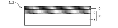
- FIG. 1 is a cross-sectional view showing an example of a laminated structure of a conductive film used for forming a temperature sensor film, and a metal thin film 10 is provided on one main surface of a resin film substrate 50.
- the temperature sensor film 110 shown in the plan view of FIG. 3 is obtained by patterning the metal thin film of the conductive film 101.
- the resin film substrate 50 may be transparent or opaque.
- the resin film substrate 50 may be made of only a resin film, or may be provided with a hard coat layer (cured resin layer) 6 on the surface of the resin film 5, as shown in FIG.
- the thickness of the resin film substrate 50 is not particularly limited, it is generally about 2 to 500 ⁇ m, preferably about 20 to 300 ⁇ m.
- An easily adhesive layer, an antistatic layer, or the like may be provided on the surface of the resin film substrate 50 (the surface of the hard coat layer 6 when the hard coat layer 6 is provided).
- the surface of the resin film substrate 50 may be subjected to treatments such as corona discharge treatment, ultraviolet irradiation treatment, plasma treatment, and sputter etching treatment for the purpose of improving the adhesion to the metal thin film 10 (or the underlayer 20). Good.
- the surface of the resin film substrate 50 on which the metal thin film 10 is formed preferably has an arithmetic average roughness Ra1 of 2 nm or less, which is obtained from a roughness curve having a length of 1 ⁇ m.
- Ra1 of the metal thin film 10 provided thereon tends to decrease.
- the smaller Ra1 of the metal thin film tends to increase the temperature coefficient of resistance (TCR).
- Ra1 of the resin film substrate 50 may be 1.5 nm or less, 1.2 nm or less, or 1.0 nm or less.
- the maximum height Rz2 of the surface of the resin film substrate 50 on which the metal thin film 10 is formed which is obtained from the roughness curve having a length of 0.7 mm, is preferably 150 nm or more. Increasing Rz2 of the film base material also increases Rz2 of the metal thin film 10 provided thereon, and tends to improve the slipperiness and blocking resistance of the conductive film.
- the surface of the resin film substrate 50 on which the metal thin film 10 is formed preferably has an arithmetic average roughness Ra2 of about 0.5 to 25 nm, more preferably 1 to 20 nm, which is obtained from a roughness curve having a length of 0.7 mm. ..
- Ra2 is within the above range, irregularities are formed on the surface of the metal thin film 10, and appropriate slipperiness can be imparted.
- Ra1 is calculated from a roughness curve with a length of 1 ⁇ m extracted from the three-dimensional surface shape measured using a scanning probe microscope.
- Ra2 and Rz2 are calculated from a roughness curve having a length of 0.7 mm extracted from the three-dimensional surface shape measured by the vertical scanning low coherence interferometry (ISO25178).
- the arithmetic average roughness Ra and the maximum height Rz both follow the definition of JIS B0601:2013.
- the resin material of the resin film 5 examples include polyester such as polyethylene terephthalate, polyimide, polyolefin, cyclic polyolefin such as norbornene, polycarbonate, polyether sulfone, and polyarylate. From the viewpoint of heat resistance, dimensional stability, electrical characteristics, mechanical characteristics, chemical resistance, etc., polyimide or polyester is preferable. Although the thickness of the resin film 5 is not particularly limited, it is generally about 2 to 500 ⁇ m, preferably about 20 to 300 ⁇ m.
- the hard coat layer 6 By providing the hard coat layer 6 on the surface of the resin film 5, the hardness of the conductive film is improved and the scratch resistance of the conductive film is increased.
- the hard coat layer 6 can be formed, for example, by applying a solution containing a curable resin on the resin film 5.
- the curable resin examples include a thermosetting resin, an ultraviolet curable resin, an electron beam curable resin and the like.
- examples of the curable resin include various resins such as polyester resins, acrylic resins, urethane resins, acryl urethane resins, amide resins, silicone resins, silicate resins, epoxy resins, melamine resins, oxetane resins, and acrylic urethane resins.
- the UV curable resin includes UV curable monomers, oligomers and polymers.
- the UV-curable resin preferably used is, for example, one having an ultraviolet-polymerizable functional group, and among them, one containing an acrylic monomer or oligomer having two or more, especially 3 to 6 functional groups as a component.
- the hard coat layer 6 may contain fine particles. By including fine particles in the hard coat layer 6, the surface shape of the surface of the resin film substrate 50 on which the metal thin film 10 is formed can be adjusted.
- various metal oxide fine particles such as silica, alumina, titania, zirconia, calcium oxide, tin oxide, indium oxide, cadmium oxide and antimony oxide, glass fine particles, polymethylmethacrylate, polystyrene, polyurethane, acryl-styrene copolymer
- a coalesced, crosslinked or uncrosslinked organic fine particles, a silicone fine particle or the like made of a polymer such as benzoguanamine, melamine or polycarbonate can be used without particular limitation.
- the average particle size of the fine particles is preferably 0.5 to 10 ⁇ m, more preferably 0.8 to 5 ⁇ m.
- unevenness is formed on the surface of the hard coat layer 6 (the surface of the resin film substrate 50) and the surface of the metal thin film 10 provided thereon.
- the sliding property and blocking resistance of the conductive film can be improved.
- the particle size of the fine particles is on the order of submicron or ⁇ m, the unevenness has an appropriate size, so that the surface becomes smooth and Ra1 tends to be small when viewed on a nm scale.
- the amount of fine particles is preferably 0.05 to 50 parts by weight, more preferably 0.1 to 30 parts by weight, based on 100 parts by weight of the resin component. ..
- the solution for forming the hard coat layer contains an ultraviolet polymerization initiator.
- the solution may contain additives such as a leveling agent, a thixotropic agent and an antistatic agent.
- the thickness of the hard coat layer 6 is not particularly limited, but in order to achieve high hardness, it is preferably 0.5 ⁇ m or more, more preferably 0.8 ⁇ m or more, still more preferably 1 ⁇ m or more. Considering the ease of formation by coating, the thickness of the hard coat layer is preferably 15 ⁇ m or less, more preferably 10 ⁇ m or less.
- the surface shape of the film base material may be adjusted by including fine particles in the order of submicron or ⁇ m in the resin film 5.
- the metal thin film 10 provided on the underlayer 20 plays a central role in temperature measurement in the temperature sensor.
- the lead portion 11 and the temperature measuring resistance portion 12 are formed as shown in FIG.
- Examples of the metal material forming the metal thin film 10 are copper, silver, aluminum, gold, rhodium, tungsten, molybdenum, zinc, tin, cobalt, indium, nickel, iron, platinum, palladium, tin, antimony, bismuth, magnesium. , And alloys thereof.
- nickel, copper, or an alloy containing these as the main components is preferable because of its low resistance, high temperature coefficient of resistance (TCR), and inexpensive material, and particularly nickel.
- a nickel alloy containing nickel as a main component is preferable.
- the thickness of the metal thin film 10 is not particularly limited, but from the viewpoint of low resistance (particularly from the viewpoint of reducing the resistance of the lead portion), 20 nm or more is preferable, 40 nm or more is more preferable, and 50 nm or more is further preferable.
- the thickness of the metal thin film 10 is preferably 500 nm or less, more preferably 300 nm or less, and further preferably 250 nm or less, from the viewpoint of shortening the film formation time, improving patterning accuracy, and the like.
- the specific resistance at a temperature of 25° C. is preferably 1.6 ⁇ 10 ⁇ 5 ⁇ cm or less, more preferably 1.5 ⁇ 10 ⁇ 5 ⁇ cm or less. ..
- the temperature coefficient of resistance (TCR) of the metal thin film 10 is preferably 3100 ppm/°C or higher, more preferably 3200 ppm/°C or higher.
- TCR is the rate of change of resistance with increasing temperature.
- Metals such as nickel and copper have the characteristic that the resistance increases linearly with the temperature rise (positive characteristic).
- the larger the TCR the larger the change in resistance with temperature changes, and the more accurate the temperature measurement in the temperature sensor film. Therefore, the larger the TCR of the metal thin film, the more preferable, but it is difficult to make the TCR larger than that of the bulk metal, and the TCR of the metal thin film is generally 6000 ppm/° C. or less.
- the metal thin film 10 preferably has an arithmetic average roughness Ra1 of 2 nm or less obtained from a roughness curve having a length of 1 ⁇ m.
- the smaller Ra1 of the metal thin film 10 tends to increase the TCR.
- Ra1 of the metal thin film 10 may be 1.5 nm or less, 1.2 nm or less, or 1.0 nm or less. It is not clear why TCR increases as Ra1 decreases, but since nano-scale irregularities are small and the metal thin film has a dense structure, having properties close to those of bulk metal contributes to the increase in TCR. It is estimated that
- the metal thin film 10 preferably has a maximum height Rz2 of 150 nm or more obtained from a roughness curve having a length of 0.7 mm.
- Rz2 of the metal thin film When the Rz2 of the metal thin film is large, the slip property is improved, the running property of the conductive film is improved, and the scratch resistance tends to be improved.
- the metal thin film 10 preferably has an arithmetic average roughness Ra2 of about 0.5 to 25 nm, more preferably 1 to 20 nm, which is determined from a roughness curve having a length of 0.7 mm. When Ra2 is within the above range, irregularities are formed on the surface of the metal thin film 10, and appropriate slipperiness can be imparted.
- the metal thin film 10 As described above, decreasing Ra1 on the surface of the metal thin film 10 tends to increase TCR, and increasing Rz2 tends to improve slipperiness.
- the metal thin film 10 is formed by a dry coating method such as a sputtering method, an uneven shape that reflects the surface shape of the resin film substrate 50 is likely to be formed on the surface of the metal thin film 10. Therefore, it is preferable that the resin film substrate 50 has a small Ra1 and a large Rz2.
- Ra1 can be kept small and Rz2 can be made large by forming a hard coat layer 6 containing fine particles having a particle size of submicron or ⁇ m order on the surface of the resin film 5 and forming a metal thin film 10 thereon. .. Further, by forming a metal thin film on the hard coat layer, mechanical strength such as scratch resistance can be improved.
- the method for forming the metal thin film is not particularly limited, and examples thereof include a film forming method such as a sputtering method, a vacuum evaporation method, an electron beam evaporation method, a chemical vapor deposition method (CVD), a chemical solution deposition method (CBD), and a plating method.
- a film forming method such as a sputtering method, a vacuum evaporation method, an electron beam evaporation method, a chemical vapor deposition method (CVD), a chemical solution deposition method (CBD), and a plating method.
- the sputtering method is preferable because a thin film having excellent film thickness uniformity can be formed. It is preferable to form the metal thin film while continuously transporting the long resin film substrate in the longitudinal direction by the roll-to-roll method.
- the length of the long conductive film is, for example, 10 m or more, and the larger the length, the better the productivity.
- the length of the long conductive film is not particularly limited, and may be appropriately set according to the allowable weight and diameter (roll diameter) of the winding rack, and is generally 10,000 m or less.
- the sputtering method is suitable for forming a metal thin film by roll-to-roll.
- a roll-to-roll sputtering device to perform film formation while continuously running a long resin film substrate in the longitudinal direction, the productivity of the conductive film can be increased.
- the metal thin film has a predetermined surface shape, whereby the slipperiness and blocking resistance of the conductive film are enhanced, scratches on the surface of the metal thin film, and winding deviation when wound in a roll shape. Etc. can be suppressed.
- the inside of the sputtering device is evacuated before starting the sputtering film formation, and the organic gas generated from the film substrate It is preferable to create an atmosphere from which impurities such as By removing the gas in the apparatus and in the film base material in advance, the amount of water, organic gas, or the like mixed into the metal thin film 10 can be reduced.
- the degree of vacuum (achievement degree of vacuum) in the sputtering apparatus before the start of sputtering film formation is, for example, 1 ⁇ 10 ⁇ 1 Pa or less, preferably 5 ⁇ 10 ⁇ 2 Pa or less, and more preferably 1 ⁇ 10 ⁇ 2 Pa or less. It is preferably 5 ⁇ 10 ⁇ 3 Pa or less and more preferably 5 ⁇ 10 ⁇ 3 Pa or less.
- a metal target is used and film formation is performed while introducing an inert gas such as argon.
- an inert gas such as argon.
- the film forming conditions for the metal thin film are not particularly limited, but it is preferable to select the film forming conditions so as to reduce the mixing of impurities into the metal thin film due to water or organic gas from the film base material.
- the film base material is processed under vacuum to remove moisture, organic gas, etc. in the film base material before the sputtering film formation. (2) Reducing damage to the film base material during sputter deposition; (3) Providing a base layer on the film base material to block moisture and organic gas from the film base material.
- the substrate temperature during the film formation may be lowered and the discharge power density may be lowered.
- the substrate temperature is preferably 200°C or lower, more preferably 150°C or lower, and further preferably 120°C or lower.
- the substrate temperature is preferably 0° C. or higher from the viewpoint of preventing embrittlement of the film substrate.
- the discharge power density is preferably 1 ⁇ 15W / cm 2, 2 ⁇ 10W / cm 2 is more preferable.
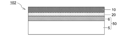
- the conductive film may include a base layer 20 between the resin film substrate 50 and the metal thin film 10.
- the base layer 20 By providing the base layer 20 on the resin film base material 50 and forming the metal thin film 10 thereon, plasma damage to the resin film base material 50 during film formation of the metal thin film 10 can be suppressed. Further, by providing the base layer 20, it is possible to block moisture, organic gas, and the like generated from the resin film base material 50, and suppress mixing of impurities into the metal thin film 10.
- the underlayer 20 is preferably an inorganic material.
- the base layer 20 may be conductive or insulating.
- the underlayer 20 may be patterned together with the metal thin film 10 when the temperature sensor film is manufactured.
- the underlayer 20 is an insulating inorganic material (inorganic dielectric)
- the underlayer 20 may or may not be patterned.
- Inorganic materials include Si, Ge, Sn, Pb, Al, Ga, In, Tl, As, Sb, Bi, Se, Te, Mg, Ca, Sr, Ba, Sc, Y, Ti, Zr, Hf, V. , Nb, Ta, Cr, Mo, W, Mn, Tc, Re, Fe, Ru, Os, Ni, Co, Rh, Ir, Pd, Pt, Cu, Ag, Au, Zn, Cd, etc.
- Silicon or silicon oxide is preferable as the material for the underlayer because it has excellent adhesion to both the resin film substrate and the metal thin film such as nickel, and has a high effect of suppressing the mixing of impurities into the metal thin film.
- a silicon oxide layer may be formed on the silicon layer.
- the base layer may include multiple layers.
- an inorganic dielectric may be formed on an inorganic conductor as a base layer, and a metal thin film may be formed thereon. In this mode, since the dielectric layer is in contact with the metal thin film, it is not necessary to pattern the underlayer 20 when manufacturing the temperature sensor film.
- the thickness of the underlayer is not particularly limited. From the viewpoint of reducing plasma damage to the film base material and enhancing the effect of blocking outgas from the film base material, the thickness of the underlayer is preferably 1 nm or more, more preferably 3 nm or more, still more preferably 5 nm or more. From the viewpoint of improving productivity and reducing material costs, the thickness of the underlayer is preferably 200 nm or less, more preferably 100 nm or less. When the underlayer 20 is composed of a plurality of layers, the total thickness is preferably within the above range.
- the method of forming the underlayer 20 is not particularly limited, and either dry coating or wet coating can be adopted.
- the metal thin film is formed by the sputtering method, it is preferable that the underlayer 20 is also formed by the sputtering method from the viewpoint of productivity.
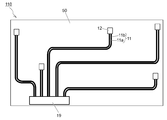
- the temperature sensor film is formed by patterning the metal thin film 10 of the conductive film. As shown in FIG. 3, in the temperature sensor film, the metal thin film has a lead portion 11 formed in a wiring shape and a temperature measuring resistance portion 12 connected to one end of the lead portion 11. The other end of the lead portion 11 is connected to the connector 19.
- the temperature measuring resistance unit 12 is a region that acts as a temperature sensor, and a temperature is measured by applying a voltage to the temperature measuring resistance unit 12 via the lead unit 11 and calculating the temperature from the resistance value.
- a temperature measuring resistance unit 12 is provided at five points on the surface.
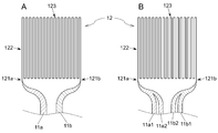
- FIG. 4A is an enlarged view of the vicinity of the temperature measuring resistance part in the two-wire type temperature sensor.
- the temperature measuring resistance portion 12 is formed by sensor wirings 122 and 123 in which a metal thin film is patterned in a thin line shape.
- the sensor wiring has a plurality of vertical electrodes 122 connected at their ends via a horizontal wiring 123 to form a hairpin-shaped bent portion, and has a zigzag pattern.
- the wiring pattern in a zigzag shape as shown in FIG. 4 the area of the temperature measuring resistance portion 12 can be made small and the length of the sensor wiring (the line length from the one end 121a to the other end 121b) can be made large.
- the pattern shape of the sensor wiring of the temperature measuring unit is not limited to the shape shown in FIG. 4, and may be a spiral pattern shape.
- the line width of the sensor wiring 122 (vertical wiring) and the distance (space width) between adjacent wirings may be set according to the patterning accuracy of photolithography.
- the line width and the space width are generally about 1 to 150 ⁇ m. From the viewpoint of preventing disconnection of the sensor wiring, the line width is preferably 3 ⁇ m or more, more preferably 5 ⁇ m or more.
- the line width is preferably 100 ⁇ m or less, and more preferably 70 ⁇ m or less from the viewpoint of increasing the resistance change and increasing the temperature measurement accuracy.
- the space width is preferably 3 to 100 ⁇ m, more preferably 5 to 70 ⁇ m.
- Both ends 121a and 121b of the sensor wiring of the resistance temperature detector 12 are connected to one ends of the lead portions 11a and 11b, respectively.
- the two lead portions 11a and 11b are formed in an elongated pattern in a state of facing each other with a slight gap therebetween, and the other end of the lead portion is connected to the connector 19.
- the lead portion is formed wider than the sensor wiring of the temperature measuring resistance portion 12 in order to secure a sufficient current capacity.
- the width of the lead portions 11a and 11b is, for example, about 0.5 to 10 mm.
- the line width of the lead portion is preferably 3 times or more, more preferably 5 times or more, and further preferably 10 times or more of the line width of the sensor wiring 122 of the temperature measuring resistance part 12.
- the connector 19 is provided with a plurality of terminals, and the plurality of lead portions are connected to different terminals.
- the connector 19 is connected to an external circuit, and when a voltage is applied between the lead portion 11a and the lead portion 11b, a current flows through the lead portion 11a, the temperature measuring resistance portion 12 and the lead portion 11b.
- the resistance value is calculated from the current value when the predetermined voltage is applied or the applied voltage when the voltage is applied so that the current has the predetermined value.
- the temperature is calculated from the resistance value based on the relational expression between the obtained resistance value and the temperature obtained in advance, or a table recording the relationship between the resistance value and the temperature.
- the resistance value obtained here includes the resistance of the lead portion 11a and the lead portion 11b in addition to the resistance of the temperature measuring resistance portion 12, but the resistance of the temperature measuring resistance portion 12 is the resistance of the lead portions 11a and 11b. Therefore, the measured value to be obtained may be regarded as the resistance of the temperature measuring resistance unit 12. From the viewpoint of reducing the influence of the resistance of the lead portion, the lead portion may be a 4-wire type.
- FIG. 4B is an enlarged view of the vicinity of the temperature measuring resistance part in the 4-wire type temperature sensor.
- the pattern shape of the resistance temperature detector 12 is similar to that of FIG. 4A.
- four lead portions 11a1, 11a2, 11b1 and 11b2 are connected to one temperature measuring resistance portion 12.
- the lead portions 11a1 and 11b1 are voltage measurement leads, and the lead portions 11a2 and 11b2 are current measurement leads.
- the voltage measuring lead 11a1 and the current measuring lead 11a2 are connected to one end 121a of the sensor wiring of the temperature measuring resistance unit 12, and the voltage measuring lead 11b1 and the current measuring lead 11b2 are the sensors of the temperature measuring resistance unit 12. It is connected to the other end 121b of the wiring.
- the resistance value of only the temperature measuring resistance portion 12 can be measured by excluding the resistance of the lead portion, so that the measurement with less error becomes possible.
- the 3-wire type may be adopted.
- the patterning method of the metal thin film is not particularly limited. It is preferable to perform patterning by a photolithography method because patterning is easy and accuracy is high.
- a photolithography on the surface of the metal thin film, an etching resist corresponding to the shape of the lead portion and the temperature measuring resistance portion is formed, and the metal thin film in the region where the etching resist is not formed is removed by wet etching, and then etching is performed. Strip the resist. Patterning of the metal thin film can also be performed by dry etching such as laser processing.
- the metal thin film 10 is formed on the resin film base material 50 by the sputtering method or the like, and the metal thin film is patterned to form a plurality of lead portions and temperature measuring resistance portions within the substrate surface. ..
- a temperature sensor element is obtained by connecting the connector 19 to the end portion of the lead portion 11 of this temperature sensor film.
- the lead portions are connected to the plurality of temperature measuring resistance portions, and the plurality of lead portions may be connected to one connector 19. Therefore, it is possible to easily form the temperature sensor element capable of measuring the temperatures at a plurality of positions in the plane.
- the metal thin film is provided on one main surface of the film substrate, but the metal thin film may be provided on both sides of the film substrate.
- the film substrate may have a hard coat layer on one side or both sides.
- the method of connecting the lead part of the temperature sensor film to the external circuit is not limited to the form via the connector.
- a controller for measuring the resistance by applying a voltage to the lead portion may be provided on the temperature sensor film.
- the lead portion and the lead wiring from the external circuit may be connected by soldering or the like without using a connector.
- the temperature sensor film has a simple structure in which a thin film is provided on the film substrate, has excellent productivity, is easy to process, and can be applied to curved surfaces. Further, since the TCR of the metal thin film is large, it is possible to realize more accurate temperature measurement. Further, in the embodiment of the present invention, since the metal thin film has a predetermined surface shape, the film is excellent in slipperiness, and the production efficiency and the yield of the temperature sensor film can be expected to improve.
- Example 1 A roll of a polyethylene terephthalate (PET) film (“Lumirror 149UNS” manufactured by Toray Co., Ltd.) having a thickness of 150 ⁇ m was set in the roll-to-roll sputter device, and the inside of the sputter device was evacuated until the ultimate vacuum reached 5 ⁇ 10 ⁇ 3 Pa. After that, argon is introduced, and DC sputtering film formation is performed under the conditions of a substrate temperature of 40° C., a pressure of 0.3 Pa, and a power density of 5.0 W/cm 2 , to produce a conductive film having a Ni thin film with a thickness of 70 nm on a PET film. did. A metallic nickel target was used to form the Ni layer.
- PET polyethylene terephthalate
- Example 2 Conductivity including a Ni thin film formed on the PI film by performing sputter deposition in the same manner as in Example 1 except that the film base material was changed to a polyimide (PI) film having a thickness of 38 ⁇ m (“Kapton 150EN” manufactured by DuPont Toray). A film was made.
- PI polyimide
- Example 3 Crosslinked polymethylmethacrylate particles with an average particle diameter of 1.5 ⁇ m (“Techpolymer SSX-101” manufactured by Sekisui Plastics) and UV-curable urethane acrylate resin (“Aika Itron” manufactured by Aika Kogyo Co., Ltd.) A coating composition using a ketone as a solvent was prepared. The amount of particles in the composition was 0.2 part by weight based on 100 parts by weight of the binder resin. This composition was applied to the surface of the PET film used in Example 1 and dried at 100° C. for 1 minute.
- Example 2 After that, a curing treatment was performed by irradiating with ultraviolet rays to form a 1.2 ⁇ m-thick hard coat layer having a surface uneven structure of microparticles. Using this hard coat film as a base material, sputter film formation was performed in the same manner as in Example 1 to produce a conductive film having a Ni thin film on the hard coat layer forming surface of the PET film.
- Example 1 The particles in the coating composition were changed to silica particles having an average particle diameter of 30 nm (“CSZ9281” manufactured by CIK Nanotech), and the amount of particles in the composition was changed to 15 parts by weight based on 100 parts by weight of the binder resin. .. Otherwise in the same manner as in Example 3, a hard coat layer was formed on the PET film, and a conductive film having a Ni thin film on the hard coat layer formation surface was produced.
- Example 2 A hard coat layer was formed on a PET film in the same manner as in Example 3 except that a coating composition containing no particles was used to prepare a conductive film having a Ni thin film on the hard coat layer formation surface.
- ⁇ Temperature coefficient of resistance> (Production of temperature sensor film)
- the conductive film was cut into a size of 10 mm ⁇ 200 mm, and the nickel layer was patterned by laser patterning into a stripe shape having a line width of 30 ⁇ m to form a temperature measuring resistance portion having a shape shown in FIG. 4A.
- the length of the pattern was adjusted so that the entire wiring resistance was about 10 k ⁇ and the resistance of the temperature measuring resistance portion was 30 times the resistance of the lead portion, and a temperature sensor film was produced.
- the temperature measuring resistance part of the temperature sensor film was set to 5°C, 25°C, and 45°C.
- the two-terminal resistance at each temperature was measured by connecting one end and the other end of the lead portion to a tester, applying a constant current and reading the voltage.
- the average value of the TCR calculated from the resistance values of 5° C. and 25° C. and the TCR calculated from the resistance values of 25° C. and 45° C. was taken as the TCR of the nickel layer.
- ⁇ Blocking resistance> A film with a smooth surface (“ZEONOR film ZF-16” manufactured by Nippon Zeon Co., Ltd.) is pressed onto the surface of the conductive film on which the Ni thin film is formed by finger pressure, and the blocking state between the films is visually observed. evaluated. ⁇ : No blocking occurred immediately after crimping ⁇ : Blocking occurred immediately after crimping, but the blocking was resolved over time ⁇ : Blocking occurred immediately after crimping, and time passed Even the blocking did not disappear
- Table 1 shows the surface roughness of the film substrate before the formation of the Ni thin film, the surface roughness of the Ni thin film of the conductive film, and the characteristics (TCR and blocking resistance) of the conductive film.
- the surface of the film substrate was smoothed and the TCR was improved, but the blocking resistance was deteriorated because Rz2 was small.
- Ra1 was larger than that in Example 1, and the TCR was lowered accordingly.
- Example 3 in which the Ni thin film was formed on the hard coat layer containing fine particles of the order of ⁇ m, Ra1 was smaller than that in Example 1, and the TCR was increased.
- the particle diameter of the fine particles contained in the hard coat layer was large, and the size of the protrusions due to the particles was large. Therefore, the arithmetic average roughness Ra1 when the surface shape was observed on the nm scale was smaller than that in Example 1. It is thought that On the other hand, in Example 3, the maximum height Rz2 on the ⁇ m scale was large due to the protrusions formed by the particles, and thus the blocking resistance was improved.
- Example 2 in which the Ni thin film was formed on the polyimide film substrate without providing the hard coat layer, high TCR and good blocking resistance were exhibited as in Example 3. From these results, it can be seen that by adjusting the surface shape of the film substrate, it is possible to form a conductive film having a large TCR and excellent blocking resistance. By providing a hard coat layer containing particles with a large particle size on a resin film, it is possible to improve both TCR and blocking resistance at the same time, as well as increase surface hardness and scratch resistance of a metal thin film. It is possible to improve the property.
Landscapes
- Physics & Mathematics (AREA)
- General Physics & Mathematics (AREA)
- Chemical & Material Sciences (AREA)
- Chemical Kinetics & Catalysis (AREA)
- Engineering & Computer Science (AREA)
- Materials Engineering (AREA)
- Mechanical Engineering (AREA)
- Metallurgy (AREA)
- Organic Chemistry (AREA)
- Physical Vapour Deposition (AREA)
- Laminated Bodies (AREA)
Abstract
導電フィルム(101)は、樹脂フィルム基材(50)の一主面上に金属薄膜(10)を備える。金属薄膜表面の長さ1μmの粗さ曲線から求められる算術平均粗さRa1は2nm以下が好ましい。金属薄膜表面の長さ0.7mmの粗さ曲線から求められる最大高さRz2は150nm以上が好ましい。樹脂フィルム基材(50)は、樹脂フィルム(5)の表面にハードコート層(6)を備えるものであってもよい。導電フィルムの金属薄膜をパターニングすることにより温度センサフィルムを作製できる。
Description
本発明は、フィルム基材上に金属薄膜を備える導電フィルム、およびフィルム基材上にパターニングされた金属薄膜を備える温度センサフィルムに関する。
電子機器には多数の温度センサが用いられている。温度センサとしては、熱電対やチップサーミスタが一般的である。熱電対やチップサーミスタ等により、面内の複数箇所の温度を測定する場合は、測定点ごとに温度センサを配置し、それぞれの温度センサをプリント配線基板等に接続する必要があるため、製造プロセスが煩雑となる。また、面内の温度分布を測定するためには基板上に多数のセンサを配置する必要があり、コストアップの要因となる。
特許文献1には、フィルム基材上に金属膜を設け、金属膜をパターニングして、測温抵抗部とリード部を形成した温度センサフィルムが提案されている。金属膜をパターニングする形態では、1層の金属膜から測温抵抗部と、測温抵抗部に接続されたリード部とを形成可能であり、個々の測温センサを配線で接続する作業を必要としない。また、フィルム基材を用いるため、可撓性に優れ、大面積化への対応も容易であるとの利点を有する。
金属膜をパターニングした温度センサでは、リード部を介して測温抵抗部に電圧を印加し、金属の抵抗値が温度により変化する特性を利用して、温度を測定する。温度測定の精度を高めるためには、温度変化に対する抵抗変化の大きい材料が好ましい。特許文献2には、ニッケルは、銅に比べて温度に対する感度(抵抗変化)が約2倍であることが記載されている。
フィルム基材上に金属薄膜を備える導電フィルムを作製し、金属薄膜をパターニングすることにより、温度センサフィルムが得られる。フィルム基材を用いる場合、ロールトゥーロールスパッタ等の連続成膜方式を採用することにより、長尺(例えば、10m~1万m程度)のフィルム基材上に、膜厚や特性が均一な金属薄膜を形成できる。
ニッケル等の金属は、温度が高いほど抵抗が大きくなる特性(正特性)を示し、バルクのニッケルは、温度上昇に対する抵抗の変化率(抵抗温度係数;TCR)が約6000ppm/℃であることが知られている。一方、本発明者らが、樹脂フィルム基材上にスパッタ法によりニッケル薄膜を形成し、その特性を評価したところ、抵抗温度係数(TCR)がバルクのニッケルの半分程度であり、温度センサフィルムとして使用する際の温度測定精度に改善の余地があることが判明した。また、長尺の樹脂フィルム基材上に金属薄膜を設けた導電フィルムは、ブロッキングに起因するフィルムの走行安定性や、金属薄膜の耐擦傷性等にも課題があることが判明した。
当該課題に鑑み、本発明は、樹脂フィルム基材上に抵抗温度係数の大きい金属薄膜を備え、かつ滑り性に優れる導電フィルムの提供を目的とする。
本発明者らは、樹脂フィルム基材上に設けられる金属薄膜が所定の表面形状を有する場合に、抵抗温度係数の上昇とフィルムの滑り性とを両立可能であることを見出し、本発明に至った。
温度センサ用導電フィルムは、樹脂フィルム基材の一主面上に金属薄膜を備える。金属薄膜表面の長さ1μmの粗さ曲線から求められる算術平均粗さRa1は2nm以下が好ましい。金属薄膜表面の長さ0.7mmの粗さ曲線から求められる最大高さRz2は150nm以上が好ましい。導電フィルムは、長尺状フィルムのロール状巻回体でもよい。
導電フィルムの金属薄膜をパターニングすることにより、温度センサフィルムを形成できる。温度センサフィルムは、樹脂フィルム基材の一主面上にパターニングされた金属薄膜を備え、金属薄膜が、測温抵抗部とリード部とにパターニングされている。樹脂フィルム基材の両面に金属薄膜が設けられていてもよい。
導電フィルムおよび温度センサフィルムの金属薄膜は、抵抗温度係数が3100ppm/℃以上であることが好ましい。金属薄膜の厚みは20~500nmが好ましい。金属薄膜は、ニッケルまたはニッケル合金からなるニッケル系薄膜であってもよい。
樹脂フィルム基材は、樹脂フィルムの表面にハードコート層を備えるものであってもよい。樹脂フィルム基材がハードコート層を備える場合、ハードコート層上に、直接または他の層を介して金属薄膜を設けることが好ましい。ハードコート層には微粒子が含まれていてもよい。
本発明の導電フィルムは、抵抗温度係数が大きく、かつ滑り性に優れている。そのため、導電フィルムをロール状に巻回した際にブロッキングが生じ難く、ロール搬送時のフィルムの走行性に優れるとともに、金属薄膜をパターニングすることにより得られる温度センサフィルムは、高い温度測定精度を実現し得る。
図1は、温度センサフィルムの形成に用いられる導電フィルムの積層構成例を示す断面図であり、樹脂フィルム基材50の一主面上に金属薄膜10を備える。この導電フィルム101の金属薄膜をパターニングすることにより、図3の平面図に示す温度センサフィルム110が得られる。
[導電フィルム]
<フィルム基材>
樹脂フィルム基材50は、透明でも不透明でもよい。樹脂フィルム基材50は、樹脂フィルムのみからなるものでもよく、図1に示すように、樹脂フィルム5の表面にハードコート層(硬化樹脂層)6を備えるものでもよい。樹脂フィルム基材50の厚みは特に限定されないが、一般には、2~500μm程度であり、20~300μm程度が好ましい。
<フィルム基材>
樹脂フィルム基材50は、透明でも不透明でもよい。樹脂フィルム基材50は、樹脂フィルムのみからなるものでもよく、図1に示すように、樹脂フィルム5の表面にハードコート層(硬化樹脂層)6を備えるものでもよい。樹脂フィルム基材50の厚みは特に限定されないが、一般には、2~500μm程度であり、20~300μm程度が好ましい。
樹脂フィルム基材50の表面(ハードコート層6が設けられている場合にはハードコート層6の表面)には、易接着層、帯電防止層等が設けられていてもよい。樹脂フィルム基材50の表面には、金属薄膜10(または下地層20)との密着性向上等を目的として、コロナ放電処理、紫外線照射処理、プラズマ処理、スパッタエッチング処理等の処理を施してもよい。
樹脂フィルム基材50の金属薄膜10形成面は、長さ1μmの粗さ曲線から求められる算術平均粗さRa1が、2nm以下であることが好ましい。フィルム基材のRa1を小さくすることにより、その上に設けられる金属薄膜10のRa1も小さくなる傾向がある。金属薄膜のRa1が小さいほど、抵抗温度係数(TCR)が大きくなる傾向がある。樹脂フィルム基材50のRa1は、1.5nm以下、1.2nm以下、または1.0nm以下であってもよい。
樹脂フィルム基材50の金属薄膜10形成面は、長さ0.7mmの粗さ曲線から求められる最大高さRz2が150nm以上であることが好ましい。フィルム基材のRz2を大きくすることにより、その上に設けられる金属薄膜10のRz2も大きくなり、導電フィルムの滑り性および耐ブロッキング性が向上する傾向がある。
樹脂フィルム基材50の金属薄膜10形成面は、長さ0.7mmの粗さ曲線から求められる算術平均粗さRa2が、0.5~25nm程度であることが好ましく、1~20nmがより好ましい。Ra2が上記範囲内であることにより、金属薄膜10表面に凹凸が形成され、適度の滑り性を付与できる。
Ra1は、走査型プローブ顕微鏡を用いて測定した三次元表面形状から抽出した長さ1μmの粗さ曲線にから算出される。Ra2およびRz2は、垂直走査型低コヒーレンス干渉法(ISO25178)により測定した三次元表面形状から抽出した長さ0.7mmの粗さ曲線から算出される。算術平均粗さRaおよび最大高さRzは、いずれもJIS B0601:2013の定義に従う。
(樹脂フィルム)
樹脂フィルム5の樹脂材料としては、ポリエチレンテレフタレート等のポリエステル、ポリイミド、ポリオレフィン、ノルボルネン系等の環状ポリオレフィン、ポリカーボネート、ポリエーテルスルフォン、ポリアリレート等が挙げられる。耐熱性、寸法安定性、電気的特性、機械的特性、耐薬品特性等の観点から、ポリイミドまたはポリエステルが好ましい。樹脂フィルム5の厚みは特に限定されないが、一般には、2~500μm程度であり、20~300μm程度が好ましい。
樹脂フィルム5の樹脂材料としては、ポリエチレンテレフタレート等のポリエステル、ポリイミド、ポリオレフィン、ノルボルネン系等の環状ポリオレフィン、ポリカーボネート、ポリエーテルスルフォン、ポリアリレート等が挙げられる。耐熱性、寸法安定性、電気的特性、機械的特性、耐薬品特性等の観点から、ポリイミドまたはポリエステルが好ましい。樹脂フィルム5の厚みは特に限定されないが、一般には、2~500μm程度であり、20~300μm程度が好ましい。
(ハードコート層)
樹脂フィルム5の表面にハードコート層6が設けられることにより、導電フィルムの硬度が向上し、導電フィルムの耐擦傷性が高められる。ハードコート層6は、例えば、樹脂フィルム5上に、硬化性樹脂を含有する溶液を塗布することにより形成できる。
樹脂フィルム5の表面にハードコート層6が設けられることにより、導電フィルムの硬度が向上し、導電フィルムの耐擦傷性が高められる。ハードコート層6は、例えば、樹脂フィルム5上に、硬化性樹脂を含有する溶液を塗布することにより形成できる。
硬化性樹脂としては、熱硬化型樹脂、紫外線硬化型樹脂、電子線硬化型樹脂等が挙げられる。硬化性樹脂の種類としてはポリエステル系、アクリル系、ウレタン系、アクリルウレタン系、アミド系、シリコーン系、シリケート系、エポキシ系、メラミン系、オキセタン系、アクリルウレタン系等の各種の樹脂が挙げられる。
これらの中でも、硬度が高く、紫外線硬化が可能で生産性に優れることから、アクリル系樹脂、アクリルウレタン系樹脂、およびエポキシ系樹脂が好ましい。紫外線硬化型樹脂には、紫外線硬化型のモノマー、オリゴマー、ポリマー等が含まれる。好ましく用いられる紫外線硬化型樹脂は、例えば紫外線重合性の官能基を有するもの、中でも当該官能基を2個以上、特に3~6個有するアクリル系のモノマーやオリゴマーを成分として含むものが挙げられる。
ハードコート層6には微粒子が含まれていてもよい。ハードコート層6に微粒子を含めることにより、樹脂フィルム基材50の金属薄膜10形成面の表面形状を調整できる。微粒子としては、シリカ、アルミナ、チタニア、ジルコニア、酸化カルシウム、酸化錫、酸化インジウム、酸化カドミウム、酸化アンチモン等の各種金属酸化物微粒子、ガラス微粒子、ポリメチルメタクリレート、ポリスチレン、ポリウレタン、アクリル-スチレン共重合体、ベンゾグアナミン、メラミン、ポリカーボネート等のポリマーからなる架橋又は未架橋の有機系微粒子、シリコーン系微粒子等を特に制限なく使用できる。
微粒子の平均粒子径は0.5~10μmが好ましく、0.8~5μmがより好ましい。サブミクロンまたはμmオーダーの平均粒子径を有する微粒子を添加することにより、ハードコート層6の表面(樹脂フィルム基材50の表面)、およびその上に設けられる金属薄膜10の表面に凹凸を形成し、導電フィルムの滑り性および耐ブロッキング性を向上できる。また、微粒子の粒子径がサブミクロンまたはμmオーダーであれば、凹凸が適度の大きさを有するため、nmスケールでみた場合には表面が平滑となり、Ra1が小さくなる傾向がある。ハードコート層の表面の全体に均一に凹凸を形成する観点から、微粒子の量は、樹脂成分100重量部に対して0.05~50重量部が好ましく、0.1~30重量部がより好ましい。
ハードコート層を形成するための溶液には、紫外線重合開始剤が配合されていることが好ましい。溶液中には、レベリング剤、チクソトロピー剤、帯電防止剤等の添加剤が含まれていてもよい。
ハードコート層6の厚みは特に限定されないが、高い硬度を実現するためには、0.5μm以上が好ましく、0.8μm以上がより好ましく、1μm以上がさらに好ましい。塗布による形成の容易性を考慮すると、ハードコート層の厚みは15μm以下が好ましく、10μm以下がより好ましい。
樹脂フィルム基材50がハードコート層を有していない場合は、樹脂フィルム5に、サブミクロンまたはμmオーダーの微粒子を含めることにより、フィルム基材の表面形状を調整してもよい。
<金属薄膜>
下地層20上に設けられる金属薄膜10は、温度センサにおける温度測定の中心的な役割を果たす。金属薄膜10をパターニングすることにより、図3に示すように、リード部11および測温抵抗部12が形成される。
下地層20上に設けられる金属薄膜10は、温度センサにおける温度測定の中心的な役割を果たす。金属薄膜10をパターニングすることにより、図3に示すように、リード部11および測温抵抗部12が形成される。
金属薄膜10を構成する金属材料の例としては、銅、銀、アルミニウム、金、ロジウム、タングステン、モリブデン、亜鉛、スズ、コバルト、インジウム、ニッケル、鉄、白金、パラジウム、スズ、アンチモン、ビスマス、マグネシウム、およびこれらの合金等が挙げられる。これらの中でも、低抵抗であり、抵抗温度係数(TCR)が高く、材料が安価であることから、ニッケル、銅、またはこれらを主成分とする(50重量%以上含む)合金が好ましく、特にニッケル、またはニッケルを主成分とするニッケル合金が好ましい。
金属薄膜10の厚みは特に限定されないが、低抵抗化の観点(特に、リード部の抵抗を小さくする観点)から、20nm以上が好ましく、40nm以上がより好ましく、50nm以上がさらに好ましい。一方、成膜時間の短縮およびパターニング精度向上等の観点から、金属薄膜10の厚みは、500nm以下が好ましく、300nm以下がより好ましく、250nm以下がさらに好ましい。
金属薄膜10がニッケル薄膜またはニッケル合金薄膜である場合、温度25℃における比抵抗は、1.6×10⁻⁵Ω・cm以下が好ましく、1.5×10⁻⁵Ω・cm以下がより好ましい。リード部の抵抗を小さくする観点からは、金属薄膜の比抵抗は小さいほど好ましく、1.2×10⁻⁵Ω・cm以下、または1.0×10⁻⁵Ω・cm以下であってもよい。金属薄膜の比抵抗は小さいほど好ましいが、バルクのニッケルよりも比抵抗を小さくすることは困難であり、一般に比抵抗は7.0×10⁻⁶Ω・cm以上である。
金属薄膜10の抵抗温度係数(TCR)は、3100ppm/℃以上が好ましく、3200ppm/℃以上がより好ましい。TCRは、温度上昇に対する抵抗の変化率である。ニッケルや銅等の金属は、温度上昇に伴って抵抗が線形的に増加する特性(正特性)を有する。正特性を有する材料のTCRは、温度T0における抵抗値R0と、温度T1における抵抗値R1から、下記式により算出される。
TCR={(R1-R0)/R0}/(T1-T0)
TCR={(R1-R0)/R0}/(T1-T0)
本明細書では、T0=25℃およびT1=5℃における抵抗値から算出されるTCRと、T0=25℃およびT1=45℃における抵抗値から算出されるTCRの平均値を金属薄膜のTCRとする。
TCRが大きいほど、温度変化に対する抵抗の変化が大きく、温度センサフィルムにおける温度測定精度が向上する。そのため、金属薄膜のTCRは大きいほど好ましいが、バルクの金属よりもTCRを大きくすることは困難であり、金属薄膜のTCRは一般に6000ppm/℃以下である。
金属薄膜10は、長さ1μmの粗さ曲線から求められる算術平均粗さRa1が、2nm以下であることが好ましい。金属薄膜10のRa1が小さいほど、TCRが大きくなる傾向がある。TCRの増加に伴って、金属薄膜をパターニングした温度センサフィルムの温度測定精度が向上する。金属薄膜10のRa1は、1.5nm以下、1.2nm以下、または1.0nm以下であってもよい。Ra1が小さいほど、TCRが大きくなる理由は定かではないが、ナノスケールでの凹凸が少なく、金属薄膜が緻密な構造を有するため、バルクの金属に近い特性を有することがTCRの上昇に寄与していると推定される。
金属薄膜10は、長さ0.7mmの粗さ曲線から求められる最大高さRz2が150nm以上であることが好ましい。金属薄膜のRz2が大きい場合に、滑り性が向上し、導電フィルムの走行性が向上するとともに、耐擦傷性が向上する傾向がある。金属薄膜10は、長さ0.7mmの粗さ曲線から求められる算術平均粗さRa2が、0.5~25nm程度であることが好ましく、1~20nmがより好ましい。Ra2が上記範囲内であることにより、金属薄膜10表面に凹凸が形成され、適度の滑り性を付与できる。
上記のように、金属薄膜10の表面のRa1を小さくすることにより、TCRが大きくなる傾向があり、Rz2を大きくすることにより滑り性が向上する傾向がある。スパッタ法等のドライコーティング法により金属薄膜10を形成する場合、金属薄膜10の表面には、樹脂フィルム基材50の表面形状を反映した凹凸形状が形成されやすい。そのため、樹脂フィルム基材50のRa1が小さく、Rz2が大きいことが好ましい。
nmスケールでの算術平均粗さRa1が小さく、かつμmスケールの最大高さRz2を大きくするためには、前述のように、粒子径がサブミクロンまたはμmオーダーの微粒子により、フィルム面における直径がサブミクロンまたはμmオーダーの突起を形成することが好ましい。樹脂フィルム5の表面に、粒子径がサブミクロンまたはμmオーダーの微粒子を含むハードコート層6を形成し、その上に金属薄膜10を形成すれば、Ra1を小さく保ち、Rz2を大きくすることができる。また、ハードコート層上に金属薄膜を形成することにより、耐擦傷性等の機械強度の向上を図ることができる。
<金属薄膜の形成方法>
金属薄膜の形成方法は特に限定されず、例えば、スパッタ法、真空蒸着法、電子ビーム蒸着法、化学気相蒸着法(CVD)、化学溶液析出法(CBD)、めっき法等の成膜方法を採用できる。これらの中でも、膜厚均一性に優れた薄膜を成膜できることから、スパッタ法が好ましい。長尺の樹脂フィルム基材を、ロールトゥーロール法により長手方向に連続的に搬送しながら、金属薄膜を成膜することが好ましい。ロールトゥーロール法により金属薄膜を成膜後の樹脂フィルム基材をロール状に巻回することにより、長尺状の導電フィルムの巻回体が得られる。長尺状の導電フィルムの長さは、例えば10m以上であり、長さが大きいほど生産性に優れる。長尺上の導電フィルムの長さは特に限定されず、巻き取り架台の許容可能な重量や直径(巻径)に応じて適宜設定すればよく、一般には1万m以下である。
金属薄膜の形成方法は特に限定されず、例えば、スパッタ法、真空蒸着法、電子ビーム蒸着法、化学気相蒸着法(CVD)、化学溶液析出法(CBD)、めっき法等の成膜方法を採用できる。これらの中でも、膜厚均一性に優れた薄膜を成膜できることから、スパッタ法が好ましい。長尺の樹脂フィルム基材を、ロールトゥーロール法により長手方向に連続的に搬送しながら、金属薄膜を成膜することが好ましい。ロールトゥーロール法により金属薄膜を成膜後の樹脂フィルム基材をロール状に巻回することにより、長尺状の導電フィルムの巻回体が得られる。長尺状の導電フィルムの長さは、例えば10m以上であり、長さが大きいほど生産性に優れる。長尺上の導電フィルムの長さは特に限定されず、巻き取り架台の許容可能な重量や直径(巻径)に応じて適宜設定すればよく、一般には1万m以下である。
ロールトゥーロールによる金属薄膜の形成には、スパッタ法が適している。ロールトゥーロールスパッタ装置を用い、長尺の樹脂フィルム基材を長手方向に連続的に走行させながら成膜を行うことにより、導電フィルムの生産性が高められる。また、前述のように、金属薄膜が所定の表面形状を有することにより、導電フィルムの滑り性および耐ブロッキング性が高められ、金属薄膜表面への傷つきや、ロール状に巻回する際の巻きズレ等を抑制できる。
ロールトゥーロールスパッタによる金属薄膜の形成においては、スパッタ装置内にロール状のフィルム基材を装填後、スパッタ成膜の開始前に、スパッタ装置内を排気して、フィルム基材から発生する有機ガス等の不純物を取り除いた雰囲気とすることが好ましい。事前に装置内およびフィルム基材中のガスを除去することにより、金属薄膜10への水分や有機ガス等の混入量を低減できる。スパッタ成膜開始前のスパッタ装置内の真空度(到達真空度)は、例えば、1×10⁻¹Pa以下であり、5×10⁻²Pa以下が好ましく、1×10⁻²Pa以下がより好ましく、5×10⁻³Pa以下がさらに好ましい。
金属薄膜のスパッタ成膜には、金属ターゲットを用い、アルゴン等の不活性ガスを導入しながら成膜が行われる。例えば、金属薄膜10としてニッケル薄膜を形成する場合は、金属Niターゲットが用いられる。金属薄膜の成膜条件は特に限定されないが、フィルム基材からの水分や有機ガス等に起因する金属薄膜への不純物の混入を低減するように成膜条件を選択することが好ましい。金属薄膜への不純物の混入を低減する方法としては、(1)前述のように、スパッタ成膜前に真空下でフィルム基材を処理して、フィルム基材中の水分や有機ガス等を除去する;(2)スパッタ成膜時のフィルム基材へのダメージを低減する;(3)フィルム基材上に下地層を設け、フィルム基材からの水分や有機ガス等を遮断する、等が挙げられる。
スパッタ成膜時のフィルム基材へのダメージを低減する方法としては、成膜時の基板温度を低くする、放電パワー密度を低くする等が挙げられる。基板温度は200℃以下が好ましく、150℃以下がより好ましく、120℃以下がさらに好ましい。一方、フィルム基材の脆化防止等の観点から、基板温度は0℃以上が好ましい。プラズマ放電を安定させつつ、フィルム基材へのダメージを抑制する観点から、放電パワー密度は、1~15W/cm2が好ましく、2~10W/cm2がより好ましい。
<下地層>
図2に示すように、導電フィルムは、樹脂フィルム基材50と金属薄膜10との間に下地層20を備えていてもよい。樹脂フィルム基材50上に下地層20を設け、その上に金属薄膜10を形成することにより、金属薄膜10成膜時の樹脂フィルム基材50へのプラズマダメージを抑制できる。また、下地層20を設けることにより、樹脂フィルム基材50から発生する水分や有機ガス等を遮断して、金属薄膜10への不純物の混入を抑制できる。
図2に示すように、導電フィルムは、樹脂フィルム基材50と金属薄膜10との間に下地層20を備えていてもよい。樹脂フィルム基材50上に下地層20を設け、その上に金属薄膜10を形成することにより、金属薄膜10成膜時の樹脂フィルム基材50へのプラズマダメージを抑制できる。また、下地層20を設けることにより、樹脂フィルム基材50から発生する水分や有機ガス等を遮断して、金属薄膜10への不純物の混入を抑制できる。
金属薄膜への有機ガスの混入を抑制する観点から、下地層20は無機材料であることが好ましい。下地層20は導電性でも絶縁性でもよい。下地層20が導電性の無機材料(無機導電体)である場合は、温度センサフィルムの作製時に金属薄膜10とともに下地層20をパターニングすればよい。下地層20が絶縁性の無機材料(無機誘電体)である場合、下地層20はパターニングしてもよく、パターニングしなくてもよい。
無機材料としては、Si,Ge,Sn,Pb,Al,Ga,In,Tl,As,Sb,Bi,Se,Te,Mg,Ca,Sr,Ba,Sc,Y,Ti,Zr,Hf,V,Nb,Ta,Cr,Mo,W,Mn,Tc,Re,Fe,Ru,Os,Ni,Co,Rh,Ir,Pd,Pt,Cu,Ag,Au,Zn,Cd等の金属元素または半金属元素、およびこれらの合金、窒化物、酸化物、炭化物、窒酸化物等が挙げられる。樹脂フィルム基材およびニッケル等の金属薄膜の両方に対する密着性に優れ、かつ金属薄膜への不純物混入抑制効果が高いことから、下地層の材料としては、シリコンまたは酸化シリコンが好ましい。下地層として、シリコン層の上に酸化シリコン層を形成してもよい。
下地層は複数の層を含んでいてもよい。例えば、下地層として無機導電体の上に無機誘電体を形成し、その上に金属薄膜を形成してもよい。この形態では、金属薄膜に誘電体層が接しているため、温度センサフィルムの作製時に、下地層20をパターニングする必要がない。
下地層の厚みは特に限定されない。フィルム基材へのプラズマダメージの低減、およびフィルム基材からのアウトガスの遮断効果を高める観点から、下地層の厚みは、1nm以上が好ましく、3nm以上がより好ましく、5nm以上がさらに好ましい。生産性向上や材料コスト低減の観点から、下地層の厚みは200nm以下が好ましく、100nm以下がより好ましい。下地層20が複数層からなる場合は、合計厚みが上記範囲であることが好ましい。
下地層20の形成方法は特に限定されず、ドライコーティング、ウェットコーティングのいずれも採用し得る。スパッタ法により金属薄膜を形成する場合は、生産性の観点から、下地層20もスパッタ法により形成することが好ましい。
[温度センサフィルム]
導電フィルムの金属薄膜10をパターニングすることにより、温度センサフィルムが形成される。図3に示すように、温度センサフィルムにおいて、金属薄膜は、配線状に形成されたリード部11と、リード部11の一端に接続された測温抵抗部12を有する。リード部11の他端は、コネクタ19に接続されている。
導電フィルムの金属薄膜10をパターニングすることにより、温度センサフィルムが形成される。図3に示すように、温度センサフィルムにおいて、金属薄膜は、配線状に形成されたリード部11と、リード部11の一端に接続された測温抵抗部12を有する。リード部11の他端は、コネクタ19に接続されている。
測温抵抗部12は、温度センサとして作用する領域であり、リード部11を介して測温抵抗部12に電圧を印加し、その抵抗値から温度を算出することにより温度測定が行われる。温度センサフィルム110の面内に複数の測温抵抗部を設けることにより、複数個所の温度を同時に測定できる。例えば、図3に示す形態では、面内の5箇所に測温抵抗部12が設けられている。
図4Aは、2線式の温度センサにおける測温抵抗部近傍の拡大図である。測温抵抗部12は、金属薄膜が細線状にパターニングされたセンサ配線122,123により形成されている。センサ配線は、複数の縦電極122が、その端部で横配線123を介して連結されてヘアピン状の屈曲部を形成し、つづら折れ状のパターンを有している。
測温抵抗部12のパターン形状を形成する細線の線幅が小さく(断面積が小さく)、測温抵抗部12のセンサ配線の一端121aから他端121bまでの線長が大きいほど、2点間の抵抗が大きく、温度変化に伴う抵抗変化量も大きいため、温度測定精度が向上する。図4に示すようなつづら折れ状の配線パターンとすることにより、測温抵抗部12の面積が小さく、かつセンサ配線の長さ(一端121aから他端121bまでの線長)を大きくできる。なお、温度測定部のセンサ配線のパターン形状は図4に示すような形態に限定されず、らせん状等のパターン形状でもよい。
センサ配線122(縦配線)の線幅、および隣接する配線間の距離(スペース幅)は、フォトリソグラフィーのパターニング精度に応じて設定すればよい。線幅およびスペース幅は、一般には1~150μm程度である。センサ配線の断線を防止する観点から、線幅は3μm以上が好ましく、5μm以上がより好ましい。抵抗変化を大きくして温度測定精度を高める観点から、線幅は100μm以下が好ましく、70μm以下がより好ましい。同様の観点から、スペース幅は3~100μmが好ましく、5~70μmがより好ましい。
測温抵抗部12のセンサ配線の両端121a,121bは、それぞれ、リード部11a、11bの一端に接続されている。2本のリード部11a,11bは、わずかな隙間を隔てて対向する状態で、細長のパターン状に形成されており、リード部の他端は、コネクタ19に接続されている。リード部は、十分な電流容量を確保するために、測温抵抗部12のセンサ配線よりも広幅に形成されている。リード部11a,11bの幅は、例えば0.5~10mm程度である。リード部の線幅は、測温抵抗部12のセンサ配線122の線幅の3倍以上が好ましく、5倍以上がより好ましく、10倍以上がさらに好ましい。
コネクタ19には複数の端子が設けられており、複数のリード部は、それぞれ異なる端子に接続されている。コネクタ19は外部回路と接続されており、リード部11aとリード部11bの間に電圧を印加することにより、リード部11a、測温抵抗部12およびリード部11bに電流が流れる。所定電圧を印加した際の電流値、または電流が所定値となるように電圧を印加した際の印加電圧から抵抗値が算出される。得られた抵抗値と、予め求められている温度との関係式、または抵抗値と温度の関係を記録したテーブル等に基づいて、抵抗値から温度が算出される。
ここで求められる抵抗値は、測温抵抗部12の抵抗に加えて、リード部11aおよびリード部11bの抵抗も含んでいるが、測温抵抗部12の抵抗は、リード部11a,11bの抵抗に比べて十分に大きいため、求められる測定値は、測温抵抗部12の抵抗とみなしてよい。なお、リード部の抵抗による影響を低減する観点から、リード部を4線式としてもよい。
図4Bは、4線式の温度センサにおける測温抵抗部近傍の拡大図である。測温抵抗部12のパターン形状は、図4Aと同様である。4線式では、1つの測温抵抗部12に4本のリード部11a1,11a2,11b1,11b2が接続されている。リード部11a1,11b1は電圧測定用リードであり、リード部11a2,11b2は電流測定用リードである。電圧測定用リード11a1および電流測定用リード11a2は、測温抵抗部12のセンサ配線の一端121aに接続されており、電圧測定用リード11b1および電流測定用リード11b2は、測温抵抗部12のセンサ配線の他端121bに接続されている。4線式では、リード部の抵抗を除外して測温抵抗部12のみの抵抗値を測定できるため、より誤差の少ない測定が可能となる。2線式および4線式以外に、3線式を採用してもよい。
金属薄膜のパターニング方法は特に限定されない。パターニングが容易であり、精度が高いことからフォトリソグラフィー法によりパターニングを行うことが好ましい。フォトリソグラフィーでは、金属薄膜の表面に、上記のリード部および測温抵抗部の形状に対応するエッチングレジストを形成し、エッチングレジストが形成されていない領域の金属薄膜をウェットエッチングにより除去した後、エッチングレジストを剥離する。金属薄膜のパターニングは、レーザ加工等のドライエッチングにより実施することもできる。
上記の実施形態では、樹脂フィルム基材50上に、スパッタ法等により金属薄膜10を形成し、金属薄膜をパターニングすることにより、基板面内に、複数のリード部および測温抵抗部を形成できる。この温度センサフィルムのリード部11の端部にコネクタ19を接続することにより、温度センサ素子が得られる。この実施形態では、複数の測温抵抗部にリード部が接続されており、複数のリード部を1つのコネクタ19と接続すればよい。そのため、面内の複数個所の温度を測定可能な温度センサ素子を簡便に形成できる。
上記の実施形態では、フィルム基材の一方の主面上に金属薄膜を設けたが、フィルム基材の両面に金属薄膜を設けてもよい。フィルム基材の両面に金属薄膜を設ける場合、フィルム基材は片面または両面にハードコート層を備えるものでもよい。
温度センサフィルムのリード部と外部回路との接続方法は、コネクタを介した形態に限定されない。例えば、温度センサフィルム上に、リード部に電圧を印加して抵抗を測定するためのコントローラを設けてもよい。また、リード部と外部回路からのリード配線とを、コネクタを介さずに半田付け等により接続してもよい。
温度センサフィルムは、フィルム基材上に薄膜が設けられた簡素な構成であり、生産性に優れるとともに、加工が容易であり、曲面への適用も可能である。また、金属薄膜のTCRが大きいため、より精度の高い温度測定を実現可能である。さらに、本発明の実施形態では、金属薄膜が所定の表面形状を有するため、フィルムの滑り性に優れ、温度センサフィルムの生産効率や歩留まりの向上が期待できる。
以下に、実施例を挙げて本発明をより詳細に説明するが、本発明は以下の実施例に限定されるものではない。
[実施例1]
ロールトゥーロールスパッタ装置内に、厚み150μmのポリエチレンテレフタレート(PET)フィルム(東レ製「ルミラー 149UNS」)のロールをセットし、スパッタ装置内を到達真空度が5×10⁻³Paとなるまで排気した後、アルゴンを導入し、基板温度40℃、圧力0.3Pa、パワー密度5.0W/cm2の条件でDCスパッタ成膜を行い、PETフィルム上に厚み70nmのNi薄膜を備える導電フィルムを作製した。Ni層の形成には、金属ニッケルターゲットを用いた。
ロールトゥーロールスパッタ装置内に、厚み150μmのポリエチレンテレフタレート(PET)フィルム(東レ製「ルミラー 149UNS」)のロールをセットし、スパッタ装置内を到達真空度が5×10⁻³Paとなるまで排気した後、アルゴンを導入し、基板温度40℃、圧力0.3Pa、パワー密度5.0W/cm2の条件でDCスパッタ成膜を行い、PETフィルム上に厚み70nmのNi薄膜を備える導電フィルムを作製した。Ni層の形成には、金属ニッケルターゲットを用いた。
[実施例2]
フィルム基材を、厚み38μmのポリイミド(PI)フィルム(東レ・デュポン製「カプトン150EN)に変更したこと以外は、実施例1と同様にスパッタ成膜を行い、PIフィルム上にNi薄膜を備える導電フィルムを作製した。
フィルム基材を、厚み38μmのポリイミド(PI)フィルム(東レ・デュポン製「カプトン150EN)に変更したこと以外は、実施例1と同様にスパッタ成膜を行い、PIフィルム上にNi薄膜を備える導電フィルムを作製した。
[実施例3]
平均粒子径1.5μmの架橋ポリメタクリル酸メチル粒子(積水化成品工業製「テクポリマー SSX-101」)と紫外線硬化型ウレタンアクリレート樹脂(アイカ工業製「アイカアイトロン」)とを含み,メチルイソブチルケトンを溶媒とするコーティング組成物を調製した。組成物中の粒子の量は、バインダー樹脂100重量部に対して,0.2重量部であった.この組成物を実施例1で用いたPETフィルムの表面に塗布し,100℃で1分間乾燥した。その後,紫外線照射により硬化処理を行い,マイクロ粒子による表面凹凸構造を有する厚み1.2μmのハードコート層を形成した.このハードコートフィルムを基材として,実施例1と同様にスパッタ成膜を行い,PETフィルムのハードコート層形成面上にNi薄膜を備える導電フィルムを作製した。
平均粒子径1.5μmの架橋ポリメタクリル酸メチル粒子(積水化成品工業製「テクポリマー SSX-101」)と紫外線硬化型ウレタンアクリレート樹脂(アイカ工業製「アイカアイトロン」)とを含み,メチルイソブチルケトンを溶媒とするコーティング組成物を調製した。組成物中の粒子の量は、バインダー樹脂100重量部に対して,0.2重量部であった.この組成物を実施例1で用いたPETフィルムの表面に塗布し,100℃で1分間乾燥した。その後,紫外線照射により硬化処理を行い,マイクロ粒子による表面凹凸構造を有する厚み1.2μmのハードコート層を形成した.このハードコートフィルムを基材として,実施例1と同様にスパッタ成膜を行い,PETフィルムのハードコート層形成面上にNi薄膜を備える導電フィルムを作製した。
[比較例1]
コーティング組成物中の粒子を平均粒子径30nmのシリカ粒子(CIKナノテック製「CSZ9281」)に変更し、組成物中の粒子の量を、バインダー樹脂100重量部に対して,15重量部に変更した。それ以外は、実施例3と同様にして、PETフィルム上にハードコート層を形成し、ハードコート層形成面上にNi薄膜を備える導電フィルムを作製した。
コーティング組成物中の粒子を平均粒子径30nmのシリカ粒子(CIKナノテック製「CSZ9281」)に変更し、組成物中の粒子の量を、バインダー樹脂100重量部に対して,15重量部に変更した。それ以外は、実施例3と同様にして、PETフィルム上にハードコート層を形成し、ハードコート層形成面上にNi薄膜を備える導電フィルムを作製した。
[比較例2]
粒子を含まないコーティング組成物を用いたこと以外は実施例3と同様にして、PETフィルム上にハードコート層を形成し、ハードコート層形成面上にNi薄膜を備える導電フィルムを作製した。
粒子を含まないコーティング組成物を用いたこと以外は実施例3と同様にして、PETフィルム上にハードコート層を形成し、ハードコート層形成面上にNi薄膜を備える導電フィルムを作製した。
[評価]
<1μm四方の表面形状の測定>
原子間力顕微鏡(Bruker製「Dimension3100」)を用い、下記の条件により三次元表面形状を測定し、長さ1μmの粗さ曲線を抽出し、JIS B0601に準じて、算術平均粗さRa1を算出した。
コントローラ:NanoscopeV
測定モード:タッピングモード
カンチレバー:Si単結晶
測定視野:1μm×1μm
<1μm四方の表面形状の測定>
原子間力顕微鏡(Bruker製「Dimension3100」)を用い、下記の条件により三次元表面形状を測定し、長さ1μmの粗さ曲線を抽出し、JIS B0601に準じて、算術平均粗さRa1を算出した。
コントローラ:NanoscopeV
測定モード:タッピングモード
カンチレバー:Si単結晶
測定視野:1μm×1μm
<0.7mm四方の表面形状の測定>
コヒーレンス走査型干渉計(Zygo NewView 7300)により、下記の条件で測定し、得られた三次元表面形状から、長さ0.7mmの粗さ曲線を抽出し、JIS B0601に準じて、算術平均粗さRa2、および最大高さRz2を算出した。
対物レンズ:10倍、ズームレンズ1倍
測定視野:0.7mm×0.7mm
Removed: None
Filter: High Pass
Filter Type: Gauss Spline
Low wavelength: 300μm
Remove spikes: on
Spike Height (xRMS): 2.5
コヒーレンス走査型干渉計(Zygo NewView 7300)により、下記の条件で測定し、得られた三次元表面形状から、長さ0.7mmの粗さ曲線を抽出し、JIS B0601に準じて、算術平均粗さRa2、および最大高さRz2を算出した。
対物レンズ:10倍、ズームレンズ1倍
測定視野:0.7mm×0.7mm
Removed: None
Filter: High Pass
Filter Type: Gauss Spline
Low wavelength: 300μm
Remove spikes: on
Spike Height (xRMS): 2.5
<抵抗温度係数>
(温度センサフィルムの作製)
導電フィルムを、10mm×200mmのサイズにカットし、レーザーパターニングにより、ニッケル層を線幅30μmのストライプ形状にパターン加工して、図4Aに示す形状の測温抵抗部を形成した。パターニングに際しては、全体の配線抵抗が約10kΩ、測温抵抗部の抵抗がリード部の抵抗の30倍となるように、パターンの長さを調整し、温度センサフィルムを作製した。
(温度センサフィルムの作製)
導電フィルムを、10mm×200mmのサイズにカットし、レーザーパターニングにより、ニッケル層を線幅30μmのストライプ形状にパターン加工して、図4Aに示す形状の測温抵抗部を形成した。パターニングに際しては、全体の配線抵抗が約10kΩ、測温抵抗部の抵抗がリード部の抵抗の30倍となるように、パターンの長さを調整し、温度センサフィルムを作製した。
(抵抗温度係数の測定)
小型の加熱冷却オーブンで、温度センサフィルムの測温抵抗部を5℃、25℃、45℃とした。リード部の一方の先端と他方の先端をテスタに接続し、定電流を流し電圧を読み取ることにより、それぞれの温度における2端子抵抗を測定した。5℃および25℃の抵抗値から計算したTCRと、25℃、45℃の抵抗値から計算したTCRの平均値を、ニッケル層のTCRとした。
小型の加熱冷却オーブンで、温度センサフィルムの測温抵抗部を5℃、25℃、45℃とした。リード部の一方の先端と他方の先端をテスタに接続し、定電流を流し電圧を読み取ることにより、それぞれの温度における2端子抵抗を測定した。5℃および25℃の抵抗値から計算したTCRと、25℃、45℃の抵抗値から計算したTCRの平均値を、ニッケル層のTCRとした。
<耐ブロッキング性>
導電フィルムのNi薄膜形成面に、表面が平滑なフィルム(日本ゼオン製、「ZEONORフィルム ZF-16」)を指圧にて圧着させ、フィルム同士のブロッキングの状態を目視により観察し、下記の基準により評価した。
○:圧着直後にブロッキングが生じていなかったもの
△:圧着直後はブロッキングが生じているが、時間の経過とともにブロッキングが解消されたもの
×:圧着直後にブロッキングが生じており、時間が経過してもブロッキングが解消しなかったもの
導電フィルムのNi薄膜形成面に、表面が平滑なフィルム(日本ゼオン製、「ZEONORフィルム ZF-16」)を指圧にて圧着させ、フィルム同士のブロッキングの状態を目視により観察し、下記の基準により評価した。
○:圧着直後にブロッキングが生じていなかったもの
△:圧着直後はブロッキングが生じているが、時間の経過とともにブロッキングが解消されたもの
×:圧着直後にブロッキングが生じており、時間が経過してもブロッキングが解消しなかったもの
Ni薄膜形成前のフィルム基材の表面粗さ、導電フィルムのNi薄膜の表面粗さ、導電フィルムの特性(TCRおよび耐ブロッキング性)を表1に示す。
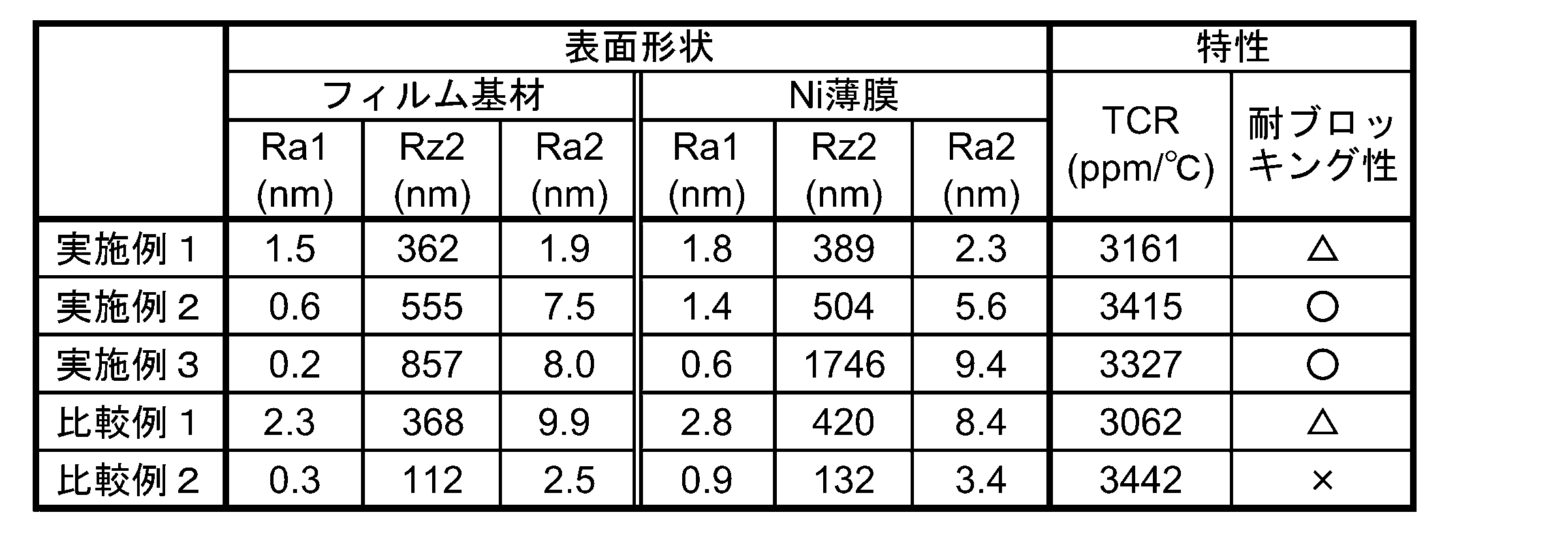
実施例および比較例では、フィルム基材のRa1が大きいほどNi薄膜のRa1が大きく、Ra1が小さいほどTCRが大きくなる傾向がみられた。また、フィルム基材のRz2が大きいほどNi薄膜のRz2が大きく、Rz2が大きいほど耐ブロッキング性が向上する傾向がみられた。
ハードコート層を設けていないフィルム基材を用いた実施例1と、粒子を含まないハードコート層を設けたフィルム基材を用いた比較例2とを対比すると、比較例2では、ハードコート層を設けたことにより、フィルム基材の表面が平滑化され、TCRが向上していたが、Rz2が小さいために、耐ブロッキング性が低下していた。nmオーダーの微粒子を含むハードコート層上にNi薄膜を形成した比較例1では、実施例1に比べてRa1が大きくなり、これに伴ってTCRが低下していた。
μmオーダーの微粒子を含むハードコート層上にNi薄膜を形成した実施例3では、実施例1よりもRa1が小さくなっており、TCRが上昇していた。実施例3では、ハードコート層に含まれる微粒子の粒子径が大きく、粒子による突起のサイズが大きいため、nmスケールで表面形状をみた場合の算術平均粗さRa1は、実施例1よりも小さくなっていると考えられる。一方、実施例3では粒子により形成された突起により、μmスケールでみた場合の最大高さRz2が大きく、これにより、耐ブロッキング性が向上していた。
ポリイミドフィルム基材上にハードコート層を設けずにNi薄膜を形成した実施例2では、実施例3と同様、高いTCRと良好な耐ブロッキング性を示した。これらの結果から、フィルム基材の表面形状を調整することにより、TCRが大きく、かつ耐ブロッキング性に優れる導電フィルムを形成可能であることが分かる。樹脂フィルム上に、粒子径の大きい粒子を含むハードコート層を設けることにより、TCRの向上と耐ブロッキング性の向上とを両立可能であることに加えて、表面硬度を高め、金属薄膜の耐擦傷性向上を図ることができる。
50 フィルム基材
5 樹脂フィルム
6 ハードコート層
20 下地層
10 金属薄膜
11 リード部
12 測温抵抗部
122,123 センサ配線
19 コネクタ
101,102 導電フィルム
110 温度センサフィルム
5 樹脂フィルム
6 ハードコート層
20 下地層
10 金属薄膜
11 リード部
12 測温抵抗部
122,123 センサ配線
19 コネクタ
101,102 導電フィルム
110 温度センサフィルム
Claims (11)
- 樹脂フィルム基材の一主面上に金属薄膜を備え、
前記金属薄膜表面の長さ1μmの粗さ曲線から求められる算術平均粗さRa1が2nm以下であり、
前記金属薄膜表面の長さ0.7mmの粗さ曲線から求められる最大高さRz2が150nm以上である、温度センサ用導電フィルム。 - 前記金属薄膜の抵抗温度係数が3100ppm/℃以上である、請求項1に記載の温度センサ用導電フィルム。
- 前記樹脂フィルム基材は、樹脂フィルムの表面にハードコート層を備え、
前記ハードコート層上に、直接または他の層を介して、前記金属薄膜が設けられている、請求項1または2に記載の温度センサ用導電フィルム。 - 前記ハードコート層が微粒子を含む、請求項3に記載の温度センサ用導電フィルム。
- 前記金属薄膜の厚みが、20~500nmである、請求項1~4のいずれか1項に記載の温度センサ用導電フィルム。
- 前記金属薄膜がニッケルまたはニッケル合金からなる、請求項1~5のいずれか1項に記載の温度センサ用導電フィルム。
- 請求項1~6のいずれか1項に記載の導電フィルムがロール状に巻回されている、導電フィルム巻回体。
- 請求項7に記載の導電フィルム巻回体を製造する方法であって、長尺状の樹脂フィルム基材を一方向に走行させながら、ロールトゥーロールスパッタにより前記金属薄膜を成膜する、導電フィルム巻回体の製造方法。
- 樹脂フィルム基材の一主面上にパターニングされた金属薄膜を備え、
前記金属薄膜が、細線にパターニングされており温度測定に用いられる測温抵抗部と、前記測温抵抗部に接続され、前記測温抵抗部よりも大きな線幅にパターニングされているリード部とにパターニングされており、
前記金属薄膜表面の長さ1μmの粗さ曲線から求められる算術平均粗さRa1が2nm以下であり、
前記金属薄膜表面の長さ0.7mmの粗さ曲線から求められる最大高さRz2が150nm以上である、温度センサフィルム。 - 前記樹脂フィルム基材は、樹脂フィルムの表面にハードコート層を備え、
前記ハードコート層上に、直接または他の層を介して、前記金属薄膜が設けられている、請求項9に記載の温度センサフィルム。 - 前記ハードコート層が微粒子を含む、請求項10に記載の温度センサフィルム。
Priority Applications (2)
| Application Number | Priority Date | Filing Date | Title |
|---|---|---|---|
| CN202080012783.9A CN113396322A (zh) | 2019-02-06 | 2020-01-24 | 导电薄膜、导电薄膜卷绕体及其制造方法、以及温度传感器薄膜 |
| KR1020217021372A KR102920966B1 (ko) | 2019-02-06 | 2020-01-24 | 도전 필름, 도전 필름 권회체 및 그 제조 방법, 그리고 온도 센서 필름 |
Applications Claiming Priority (2)
| Application Number | Priority Date | Filing Date | Title |
|---|---|---|---|
| JP2019020159A JP7373284B2 (ja) | 2019-02-06 | 2019-02-06 | 導電フィルム、導電フィルム巻回体およびその製造方法、ならびに温度センサフィルム |
| JP2019-020159 | 2019-02-06 |
Publications (1)
| Publication Number | Publication Date |
|---|---|
| WO2020162237A1 true WO2020162237A1 (ja) | 2020-08-13 |
Family
ID=71947631
Family Applications (1)
| Application Number | Title | Priority Date | Filing Date |
|---|---|---|---|
| PCT/JP2020/002637 Ceased WO2020162237A1 (ja) | 2019-02-06 | 2020-01-24 | 導電フィルム、導電フィルム巻回体およびその製造方法、ならびに温度センサフィルム |
Country Status (5)
| Country | Link |
|---|---|
| JP (1) | JP7373284B2 (ja) |
| KR (1) | KR102920966B1 (ja) |
| CN (1) | CN113396322A (ja) |
| TW (1) | TWI859188B (ja) |
| WO (1) | WO2020162237A1 (ja) |
Families Citing this family (1)
| Publication number | Priority date | Publication date | Assignee | Title |
|---|---|---|---|---|
| JP7558027B2 (ja) * | 2020-10-15 | 2024-09-30 | ジオマテック株式会社 | 薄膜熱電対素子、測温素子及び薄膜熱電対素子の製造方法 |
Citations (4)
| Publication number | Priority date | Publication date | Assignee | Title |
|---|---|---|---|---|
| JPH07333073A (ja) * | 1994-06-07 | 1995-12-22 | Casio Comput Co Ltd | 温度センサおよびこれを用いた温度測定器 |
| JP2007232669A (ja) * | 2006-03-03 | 2007-09-13 | Tokyo Univ Of Agriculture & Technology | 温度センサおよびその製造方法 |
| WO2008143011A1 (ja) * | 2007-05-11 | 2008-11-27 | Mitsui Mining & Smelting Co., Ltd. | 薄膜センサ、薄膜センサモジュールおよび薄膜センサの製造方法 |
| JP2019001002A (ja) * | 2017-06-12 | 2019-01-10 | 日東電工株式会社 | 導電性フィルム |
Family Cites Families (6)
| Publication number | Priority date | Publication date | Assignee | Title |
|---|---|---|---|---|
| JP3733962B2 (ja) | 2003-09-12 | 2006-01-11 | 山里産業株式会社 | 薄膜抵抗測温シート |
| TW200916745A (en) * | 2007-07-09 | 2009-04-16 | Kobe Steel Ltd | Temperature-measuring member, temperature-measuring device, and method for measuring temperature |
| JP5515554B2 (ja) * | 2009-09-18 | 2014-06-11 | 凸版印刷株式会社 | 透明導電性薄膜の製造方法 |
| JP5932098B2 (ja) * | 2014-04-17 | 2016-06-08 | 日東電工株式会社 | 透明導電性フィルム |
| JP6433707B2 (ja) * | 2014-07-28 | 2018-12-05 | 日東電工株式会社 | 透明導電性積層体およびその製造方法、透明導電性フィルムの製造方法、ならびに透明導電性フィルム巻回体の製造方法 |
| JP6953170B2 (ja) * | 2017-04-19 | 2021-10-27 | 日東電工株式会社 | 導電性フィルムおよびタッチパネル |
-
2019
- 2019-02-06 JP JP2019020159A patent/JP7373284B2/ja active Active
-
2020
- 2020-01-24 WO PCT/JP2020/002637 patent/WO2020162237A1/ja not_active Ceased
- 2020-01-24 KR KR1020217021372A patent/KR102920966B1/ko active Active
- 2020-01-24 CN CN202080012783.9A patent/CN113396322A/zh active Pending
- 2020-02-05 TW TW109103516A patent/TWI859188B/zh active
Patent Citations (4)
| Publication number | Priority date | Publication date | Assignee | Title |
|---|---|---|---|---|
| JPH07333073A (ja) * | 1994-06-07 | 1995-12-22 | Casio Comput Co Ltd | 温度センサおよびこれを用いた温度測定器 |
| JP2007232669A (ja) * | 2006-03-03 | 2007-09-13 | Tokyo Univ Of Agriculture & Technology | 温度センサおよびその製造方法 |
| WO2008143011A1 (ja) * | 2007-05-11 | 2008-11-27 | Mitsui Mining & Smelting Co., Ltd. | 薄膜センサ、薄膜センサモジュールおよび薄膜センサの製造方法 |
| JP2019001002A (ja) * | 2017-06-12 | 2019-01-10 | 日東電工株式会社 | 導電性フィルム |
Also Published As
| Publication number | Publication date |
|---|---|
| KR20210124211A (ko) | 2021-10-14 |
| JP7373284B2 (ja) | 2023-11-02 |
| CN113396322A (zh) | 2021-09-14 |
| TWI859188B (zh) | 2024-10-21 |
| JP2020126033A (ja) | 2020-08-20 |
| KR102920966B1 (ko) | 2026-01-30 |
| TW202045353A (zh) | 2020-12-16 |
Similar Documents
| Publication | Publication Date | Title |
|---|---|---|
| JP7345341B2 (ja) | 導電フィルム、導電フィルム巻回体およびその製造方法、ならびに温度センサフィルム | |
| US12135247B2 (en) | Electroconductive film, method for manufacturing same, temperature sensor film, and method for manufacturing same | |
| KR102920966B1 (ko) | 도전 필름, 도전 필름 권회체 및 그 제조 방법, 그리고 온도 센서 필름 | |
| TWI886154B (zh) | 導電膜、溫度感測膜及導電膜之製造方法 | |
| US12146799B2 (en) | Temperature sensor film, conductive film and method for producing same | |
| KR102954585B1 (ko) | 도전 필름 및 온도 센서 필름 | |
| KR102954678B1 (ko) | 도전 필름 및 그 제조 방법, 그리고 온도 센서 필름 및 그 제조 방법 | |
| KR102954674B1 (ko) | 온도 센서 필름, 도전 필름 및 그 제조 방법 | |
| KR102954606B1 (ko) | 도전 필름, 도전 필름의 제조 방법 및 온도 센서 필름 |
Legal Events
| Date | Code | Title | Description |
|---|---|---|---|
| 121 | Ep: the epo has been informed by wipo that ep was designated in this application |
Ref document number: 20752285 Country of ref document: EP Kind code of ref document: A1 |
|
| ENP | Entry into the national phase |
Ref document number: 20217021372 Country of ref document: KR Kind code of ref document: A |
|
| NENP | Non-entry into the national phase |
Ref country code: DE |
|
| 122 | Ep: pct application non-entry in european phase |
Ref document number: 20752285 Country of ref document: EP Kind code of ref document: A1 |