WO2020158952A1 - 振動センサ - Google Patents
振動センサ Download PDFInfo
- Publication number
- WO2020158952A1 WO2020158952A1 PCT/JP2020/003828 JP2020003828W WO2020158952A1 WO 2020158952 A1 WO2020158952 A1 WO 2020158952A1 JP 2020003828 W JP2020003828 W JP 2020003828W WO 2020158952 A1 WO2020158952 A1 WO 2020158952A1
- Authority
- WO
- WIPO (PCT)
- Prior art keywords
- substrate
- vibration sensor
- main surface
- convex member
- region
- Prior art date
- Legal status (The legal status is an assumption and is not a legal conclusion. Google has not performed a legal analysis and makes no representation as to the accuracy of the status listed.)
- Ceased
Links
Images





Classifications
-
- G—PHYSICS
- G01—MEASURING; TESTING
- G01H—MEASUREMENT OF MECHANICAL VIBRATIONS OR ULTRASONIC, SONIC OR INFRASONIC WAVES
- G01H11/00—Measuring mechanical vibrations or ultrasonic, sonic or infrasonic waves by detecting changes in electric or magnetic properties
- G01H11/06—Measuring mechanical vibrations or ultrasonic, sonic or infrasonic waves by detecting changes in electric or magnetic properties by electric means
- G01H11/08—Measuring mechanical vibrations or ultrasonic, sonic or infrasonic waves by detecting changes in electric or magnetic properties by electric means using piezoelectric devices
-
- H—ELECTRICITY
- H10—SEMICONDUCTOR DEVICES; ELECTRIC SOLID-STATE DEVICES NOT OTHERWISE PROVIDED FOR
- H10N—ELECTRIC SOLID-STATE DEVICES NOT OTHERWISE PROVIDED FOR
- H10N30/00—Piezoelectric or electrostrictive devices
- H10N30/01—Manufacture or treatment
- H10N30/02—Forming enclosures or casings
-
- H—ELECTRICITY
- H10—SEMICONDUCTOR DEVICES; ELECTRIC SOLID-STATE DEVICES NOT OTHERWISE PROVIDED FOR
- H10N—ELECTRIC SOLID-STATE DEVICES NOT OTHERWISE PROVIDED FOR
- H10N30/00—Piezoelectric or electrostrictive devices
- H10N30/30—Piezoelectric or electrostrictive devices with mechanical input and electrical output, e.g. functioning as generators or sensors
- H10N30/302—Sensors
-
- H—ELECTRICITY
- H10—SEMICONDUCTOR DEVICES; ELECTRIC SOLID-STATE DEVICES NOT OTHERWISE PROVIDED FOR
- H10N—ELECTRIC SOLID-STATE DEVICES NOT OTHERWISE PROVIDED FOR
- H10N30/00—Piezoelectric or electrostrictive devices
- H10N30/80—Constructional details
- H10N30/802—Circuitry or processes for operating piezoelectric or electrostrictive devices not otherwise provided for, e.g. drive circuits
-
- H—ELECTRICITY
- H10—SEMICONDUCTOR DEVICES; ELECTRIC SOLID-STATE DEVICES NOT OTHERWISE PROVIDED FOR
- H10N—ELECTRIC SOLID-STATE DEVICES NOT OTHERWISE PROVIDED FOR
- H10N30/00—Piezoelectric or electrostrictive devices
- H10N30/80—Constructional details
- H10N30/87—Electrodes or interconnections, e.g. leads or terminals
- H10N30/875—Further connection or lead arrangements, e.g. flexible wiring boards, terminal pins
-
- H—ELECTRICITY
- H10—SEMICONDUCTOR DEVICES; ELECTRIC SOLID-STATE DEVICES NOT OTHERWISE PROVIDED FOR
- H10N—ELECTRIC SOLID-STATE DEVICES NOT OTHERWISE PROVIDED FOR
- H10N30/00—Piezoelectric or electrostrictive devices
- H10N30/80—Constructional details
- H10N30/88—Mounts; Supports; Enclosures; Casings
-
- H—ELECTRICITY
- H10—SEMICONDUCTOR DEVICES; ELECTRIC SOLID-STATE DEVICES NOT OTHERWISE PROVIDED FOR
- H10N—ELECTRIC SOLID-STATE DEVICES NOT OTHERWISE PROVIDED FOR
- H10N30/00—Piezoelectric or electrostrictive devices
- H10N30/80—Constructional details
- H10N30/88—Mounts; Supports; Enclosures; Casings
- H10N30/883—Additional insulation means preventing electrical, physical or chemical damage, e.g. protective coatings
-
- G—PHYSICS
- G01—MEASURING; TESTING
- G01L—MEASURING FORCE, STRESS, TORQUE, WORK, MECHANICAL POWER, MECHANICAL EFFICIENCY, OR FLUID PRESSURE
- G01L1/00—Measuring force or stress, in general
- G01L1/16—Measuring force or stress, in general using properties of piezoelectric devices
Definitions
- the present invention relates to a vibration sensor.
- a vibration sensor having a piezoelectric element is brought into contact with an object that can generate vibration, and the vibration from the object is detected by the piezoelectric element and converted into an electrical signal and output.
- a vibration sensor when vibration is transmitted from an object to a piezoelectric element, the piezoelectric element is displaced to generate an electric signal, and the generated electric signal is subjected to a predetermined amplification process to output the amplified signal. Output. At this time, it is desirable to efficiently transmit the vibration from the object to the piezoelectric element and suppress the EMI noise from mixing in the signal generated by the piezoelectric element to improve the vibration detection accuracy of the vibration sensor. Be done.
- the present invention has been made in view of the above, and an object thereof is to obtain a vibration sensor suitable for improving vibration detection accuracy.
- a vibration sensor has a first main surface and a second main surface arranged on the opposite side of the first main surface. It has a substrate, a piezoelectric element arranged on the 2nd principal surface, and a conductive film arranged on the 1st principal surface.
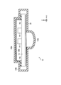
- FIG. 1 is a cross-sectional view showing the configuration of the vibration sensor according to the embodiment.
- FIG. 2 is a plan view showing the configuration of the vibration sensor according to the embodiment.
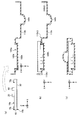
- FIG. 3 is a cross-sectional view showing the operation of the vibration sensor according to the embodiment (when the substrate is fixed in a doubly supported beam shape).
- FIG. 4 is a cross-sectional view showing the operation of the vibration sensor according to the embodiment (when the substrate is fixed in a cantilever shape).
- FIG. 5: is sectional drawing which shows operation
- FIG. 6 is a plan view showing the configuration of the vibration sensor according to the first modified example of the embodiment.
- FIG. 1 is a cross-sectional view showing the configuration of the vibration sensor according to the embodiment.
- FIG. 2 is a plan view showing the configuration of the vibration sensor according to the embodiment.
- FIG. 3 is a cross-sectional view showing the operation of the vibration sensor according to the embodiment (when the substrate is
- FIG. 7 is a cross-sectional view showing the configuration of the vibration sensor according to the second modification of the embodiment.
- FIG. 8 is a sectional view showing the operation of the vibration sensor according to the second modification of the embodiment.
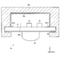
- FIG. 9 is a cross-sectional view showing the configuration of the vibration sensor according to the third modification of the embodiment.
- FIG. 10 is a cross-sectional view showing the configuration of the vibration sensor according to the fourth modified example of the embodiment.
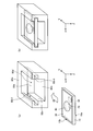
- FIG. 11 is a process cross-sectional view showing the method of manufacturing the vibration sensor according to the fourth modification of the embodiment.
- FIG. 12 is a plan view showing the method of manufacturing the vibration sensor according to the fourth modification of the embodiment.
- FIG. 13 is a cross-sectional view showing the configuration of the vibration sensor according to the fifth modified example of the embodiment.
- FIG. 14 is a perspective view showing the method of manufacturing the vibration sensor according to the fifth modification of the embodiment.
- the vibration sensor according to the embodiment has a piezoelectric element, is brought into contact with an object, detects vibration from the object by the piezoelectric element, converts the vibration into an electric signal, and outputs the electric signal.
- the object includes any object that can generate vibration.
- the vibration sensor if the vibration from the object can be more efficiently transmitted to the piezoelectric element, the sensitivity of the sensor can be increased, and the vibration detection accuracy can be expected to be improved in terms of the sensitivity. Further, in the vibration sensor, if it is possible to further suppress the mixing of EMI noise (electromagnetic wave noise) due to an external electromagnetic wave, the S/N ratio for the same sensitivity can be increased, and the vibration detection accuracy can be improved in terms of the S/N ratio. It can be expected to improve.
- EMI noise electromagnetic wave noise
- the piezoelectric element is arranged on the main surface of the substrate opposite to the object, and the conductive film is provided on the object-side main surface.
- the board structurally improve the board so that it can be easily bent.
- components are mounted on one surface (main surface opposite to the object) of the front surface, and a structure convex on the back surface (convex member) to bend the board from the back surface (main surface on the object side) side. ) Is provided.
- the substrate is easily bent via the convex member.
- the force due to the vibration can be efficiently applied from the substrate to the piezoelectric element, and the force and frequency can be efficiently detected by the piezoelectric element.
- the back surface is entirely covered with a conductive film and the conductive film is electrically connected to the ground potential. Thereby, the path of the piezoelectric element and its output signal can be shielded from electromagnetic noise.
- FIG. 1 is a cross-sectional view showing the configuration of the vibration sensor 1.
- FIG. 2 is a plan view showing the configuration of the vibration sensor 1.
- the direction perpendicular to the surface of the substrate is the Z direction
- two directions orthogonal to each other in the plane perpendicular to the Z direction are the X direction and the Y direction.
- 2A is a plan view when the substrate is viewed from the +Z side
- FIG. 2B is a plan view when the substrate is viewed from the ⁇ Z side.
- the vibration sensor 1 has a substrate 10, a piezoelectric element 20, a conductive film 30, a convex member 40, and an element 50.
- the substrate 10 has a substantially plate shape extending in the XY directions and has a front surface (second main surface) 10a and a back surface (first main surface) 10b.
- the substrate 10 may have a rectangular shape, a substantially rectangular shape, or a substantially square shape in the XY plan view.
- the substrate 10 may have a size of 15 mm ⁇ 15 mm ⁇ 0.8 mm (width), for example.
- FIG. 2A illustrates a case where the substrate 10 has a substantially rectangular shape with the X direction as the longitudinal direction.
- the front surface 10a and the back surface 10b are main surfaces facing each other.
- the back surface 10b extends in the XY directions.
- the back surface 10b is a surface that receives vibration, and can be a main surface on the side of an object (for example, a part of a human body) that the vibration sensor 1 contacts when the vibration sensor 1 is used.
- the surface 10a extends in the XY directions.
- the surface 10a serves as a main surface opposite to the object.
- the substrate 10 may be formed of an insulating material, and may be formed of a material containing an insulating resin (for example, glass epoxy) or an insulating ceramic (for example, alumina) as a main component.
- the substrate 10 may be a metal plate or an alloy plate whose surface 10a is insulation-treated. Further, in FIG. 2, the planar shape of the substrate 10 is a rectangle, but the left and right sides are long enough to be held.
- it may have a structure such as a circle, an ellipse, a rhombus or the like, which is cut out at both sides and provided with a straight side edge having a side and holding it there.
- the piezoelectric element 20 is arranged on the surface 10 a of the substrate 10. As shown in FIG. 2A, the piezoelectric element 20 can be arranged near the center of the substrate 10 in XY plan view. The piezoelectric element 20 may be fixedly supported on the surface 10 a of the substrate 10. The piezoelectric element 20 may have a size of 3.2 mm ⁇ 1.6 mm ⁇ 0.8 (width), for example. When the area of the surface 10a of the substrate 10 that overlaps the convex member 40p when seen through from the Z direction is called the fixing area of the convex member 40p, the piezoelectric element 20 is positioned within the fixing area of the convex member 40p. To do.
- the piezoelectric element 20 shown in FIG. 1 has a piezoelectric body 21, a terminal electrode 22, and a terminal electrode 23.
- the piezoelectric body 21 may have a single plate structure.
- the piezoelectric body 21 may be formed of a material exhibiting piezoelectricity, and may be formed of, for example, a material containing PZT (lead zirconate titanate) as a main component.
- the piezoelectric body 21 may be provided with polarization terminals on the +Z side and the ⁇ Z side in advance, and may be polarized by applying a predetermined voltage from the XY directions, and the polarization direction may be the Z direction.
- the terminal electrode 22 and the terminal electrode 23 are arranged on opposite sides of the piezoelectric body 21.
- the terminal electrode 22 may be arranged on the ⁇ X side of the piezoelectric body 21, and the terminal electrode 23 may be arranged on the +X side of the piezoelectric body 21.
- the vibration modes of the piezoelectric element include a d33 mode when vibrating in the polarization direction and a d31 mode or d32 mode when vibrating in the direction orthogonal to the polarization direction.
- the d33 mode is the vibration mode in the Z direction
- the d31 mode is the vibration mode in the X direction
- the d32 mode is the vibration mode in the Y direction.
- the piezoelectric element 20 has better excitation efficiency and higher sensitivity when the piezoelectric element 20 is mounted on a substrate so that the d31 mode is in the X direction and is displaced in the X direction d31 mode than in the Z direction d33 mode.
- a conductive pattern is provided on the surface 10a of the substrate 10, and the conductive pattern is formed with electrodes and wirings integrated with the electrodes.
- the terminal electrode 22 and the terminal electrode 23 are on the surface 10a of the substrate 10, respectively. It may be bonded to the electrode with a conductive bonding material such as solder. That is, the piezoelectric element 20 is electrically connected to the conductive pattern.
- the conductive pattern and the piezoelectric element 20 may each be covered with an insulating resin.
- the wiring is electrically connected to the element 50 to realize a desired circuit configuration.
- the element 50 may be electrically connected to the piezoelectric element 20 via a wiring.
- the element 50 is arranged on the surface 10 a of the substrate 10.
- the element 50 is a peripheral component for the piezoelectric element 20, and may be, for example, a semiconductor element such as a FET (Field Effect Transistor) that performs an amplification process on a signal generated in the piezoelectric element 20.
- the element 50 can be arranged around the piezoelectric element 20 in XY plan view.
- the element 50 may be fixedly supported on the surface 10a of the substrate 10.
- the element 50 may have a plurality of terminal electrodes, and the plurality of terminal electrodes may be joined to the electrodes on the surface 10a of the substrate 10 with a conductive joining material such as solder.
- the element 50 is provided in the fixing region of the convex member 40p. It may be provided, or may be provided in a region other than the fixed region.
- the conductive film 30 is arranged on the back surface 10b of the substrate 10.
- the conductive film 30 may extend from the periphery of the substrate 10 and the convex member 40 in the XY direction between the side edges of the substrate 10, and as shown in FIG. It may extend to the outside.
- the conductive film 30 may be continuously arranged on the back surface 10b of the substrate 10 or may be discontinuously arranged in a mesh shape. Further, the conductive film 30 may cover the region including the piezoelectric element 20 and having a large area outside the piezoelectric element 20 when viewed from the Z direction on the back surface 10b.
- the conductive film 30 may cover the region including the piezoelectric element 20 and the element 50 and having a large area outside each of the piezoelectric element 20 and the element 50 on the back surface 10b when seen through from the Z direction. As shown in FIGS. 1 and 2B, the conductive film 30 may entirely cover the back surface 10b of the substrate 10. In FIG. 2, the conductive film 30 is covered over the entire area of the substrate 10 with a slight space (a portion where the lead wire 10 is in contact) inward from each side.
- the conductive film 30 may be formed of a material having a metal (for example, copper or aluminum) as a main component.
- the conductive film 30 may be electrically connected to the ground potential, as shown by the wavy line in FIG. Thereby, for example, when electromagnetic wave noise arrives from the ⁇ Z side, the electromagnetic wave noise can be converted into a noise current such as an induced current by the conductive film 30, and the converted noise current is converted from the conductive film 30 to the ground potential. Since it can escape, the piezoelectric element 20, the other element 50, and their signal paths can be shielded from electromagnetic noise.
- the convex member 40 is arranged on the back surface 10 b of the substrate 10. As shown in FIG. 2B, the convex member 40 can be arranged at a position corresponding to the piezoelectric element 20 on the back surface 10b of the substrate 10.
- the convex member 40 may be arranged at a position including the piezoelectric element 20 on the back surface 10b when viewed from the Z direction, and the center of the convex member 40 is arranged at a position overlapping the piezoelectric element 20. May be.
- the plane width of the convex member 40 (the lengths of the long axis and the short axis since it is an ellipse) is significantly smaller than the plane width of the substrate 10.
- the convex member 40 may have a size of, for example, a diameter of 9.5 mm and a height of 4.0 mm. As shown in FIG. 2B, the plane width of the convex member 40 in the X direction is significantly smaller than the plane width of the substrate 10 in the X direction.
- the plane width of the convex member 40 in the Y direction is significantly smaller than the plane width of the substrate 10 in the Y direction.
- the plane width of the convex member 40 may be smaller than the plane width of the conductive film 30.
- the plane width of the convex member 40 in the X direction may be smaller than the plane width of the conductive film 30 in the X direction.
- the plane width of the convex member 40 in the Y direction may be smaller than the plane width of the conductive film 30 in the Y direction.
- the convex member 40 can be fixed to the back surface 10b of the substrate 10 and bulges in the ⁇ Z direction from the back surface 10b of the substrate 10.
- the convex member 40 may be fixed to the back surface 10b of the substrate 10 at substantially the center of the substrate 10.
- the convex member 40 may be in contact with the conductive film 30, and projects downward from the back side of the substrate with respect to the conductive film 30 (see FIG. 1 ).
- the convex member 40 may be formed of any material capable of transmitting stress due to vibration to the substrate 10.
- the convex member 40 is made of metal, the convex member 40 may be fixed to the back surface 10b of the substrate 10 by alloying the convex member 40 to the conductive film 30.
- the convex member 40 When the convex member 40 is made of a material other than metal, the convex member 40 is adhered to the conductive film 30 with an adhesive or the like, so that the convex member 40 is fixed to the back surface 10b of the substrate 10. Good.
- the convex member 40 When the convex member 40 is made of metal, the convex member 40 may be fixed to the back surface 10b of the substrate 10 by being fixed to the conductive film 30 with an adhesive.
- the adhesive may be a fixing agent having electrical conductivity and adhesiveness, and is, for example, a brazing material, a conductive paste, a conductive resin, or the like.
- the material of the adhesive used in this embodiment may be an acrylic instant adhesive.
- the elastic modulus is, for example, 8 MPa.
- the convex member 40 has at least a flat surface 40a and a convex surface 40b.
- the flat surface 40a extends flat in the XY directions.
- the flat surface 40a is a fixing surface to which the convex member 40 is fixed to the back surface 10b of the substrate 10.
- the convex surface 40b projects in the ⁇ Z direction from the end of the flat surface 40a (the surface that contacts the substrate 10).
- the convex surface 40b extends perpendicularly to the ⁇ Z direction from the end of the flat surface 40a and forms a closed surface along with the flat surface 40a from the middle.
- the convex surface 40b can form a curved surface that is convex in the ⁇ Z direction.
- the convex surface 40b may include a cylindrical surface 40b2 and a bulging surface 40b1.
- the cylindrical surface 40b2 is a surface extending in a substantially cylindrical shape in the Z direction while keeping the dimension in the X direction substantially constant, and may have a substantially circular shape or a substantially elliptical shape in XY plan view. Good.
- the convex member 40 may be fixed to the back surface 10b at an approximately flat center 40a of the substrate 10 by an adhesive material with a flat surface 40a.
- the portion 10b2 of the protruding member 40 is a tubular member having a circular or elliptical cross section cut in the horizontal direction.
- Reference numeral 40b1 is a member that is bulged like a lens from the tubular member, and has a shape like a circular ball or an elliptical ball that is sliced.
- FIG. 2B illustrates a case where the cylindrical surface 40b2 has a substantially elliptical shape in XY plan view.
- the bulging surface 40b1 is convexly curved and bulges from the ⁇ Z side end of the cylindrical surface 40b2, and is arcuate from the ⁇ Z side end of the cylindrical surface 40b2 toward the ⁇ Z side in the XZ sectional view. It bulges out.
- the bulging surface 40b1 may be a substantially spherical surface or an aspherical surface.
- the convex member 40 may be configured by the bulging surface 40b1 with the cylindrical surface 40b2 omitted.
- the convex member 40 is a member that receives vibration, and is brought into contact with an object (for example, a part of a human body) when the vibration sensor 1 is used.
- the substrate 10 may be fixed in a cantilever shape by another member that can be fixed so that the force due to the vibration received by the convex member 40 can be transmitted to the substrate 10. It may be fixed in a doubly supported beam shape.
- the vibration sensor 1 when the vibration sensor 1 is attached to an appropriate position such as an arm, a wrist or a neck of a human body so that the convex member 40 is brought into contact with the skin of the human body with a medical fixing tape or the like, the other substrate 10 can be fixed. It is equivalent to being fixed in the shape of a doubly supported beam by a member.
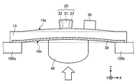
- the substrate 10 is fixed in a doubly supported beam shape by other members 100a and 100b, for example. If the substrate 10 has a substantially rectangular shape in the XY plan view, two short sides of the substrate 10 may be supported. In this case, when the convex member 40 receives a force due to vibration from an object (for example, a part of a human body) as indicated by a white arrow, the force is transmitted from the convex member 40 to the substrate 10, 10 is displaced from the position shown by the broken line to the position shown by the solid line, which causes vertical bending.
- FIG. 3 is a cross-sectional view showing the operation of the vibration sensor 1 (when the substrate is fixed in a doubly supported beam shape).
- the convex member 40 can efficiently bend the substrate 10. Further, since the convex member 40 is arranged at the position corresponding to the piezoelectric element 20 on the back surface 10b of the substrate 10, it is possible to efficiently bend the region on the front surface 10a of the substrate 10 near the piezoelectric element 20. Thereby, the piezoelectric body 21 in the piezoelectric element 20 can be efficiently displaced, and the force due to vibration can be detected by the piezoelectric element 20 with high sensitivity.
- the substrate 10 is fixed in a cantilever shape by another member 100a, for example.
- the substrate 10 has a substantially rectangular shape in the XY plan view, one short side of the substrate 10 may be supported.
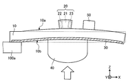
- the convex member 40 receives a force due to vibration from an object (for example, a part of the human body) as indicated by the white arrow, the force is transmitted from the convex member 40 to the substrate 10, and the substrate 10 is The position indicated by the broken line can be displaced to the position indicated by the solid line to bend.
- FIG. 4 is a cross-sectional view showing the operation of the vibration sensor 1 (when the substrate is fixed in a cantilever shape).
- the convex member 40 can efficiently bend the substrate 10. Further, since the convex member 40 is arranged at the position corresponding to the piezoelectric element 20 on the back surface 10b of the substrate 10, it is possible to efficiently bend the region on the front surface 10a of the substrate 10 near the piezoelectric element 20. Thereby, the piezoelectric body 21 in the piezoelectric element 20 can be efficiently displaced, and the force due to vibration can be detected by the piezoelectric element 20 with high sensitivity.
- the piezoelectric element 20 is arranged on the surface 10a of the substrate 10 opposite to the object, and the conductive film 30 and the conductive film 30 are formed on the object-side back surface 10b. And a convex member 40 which is projected. As a result, it is possible to efficiently transmit (force by) vibration to the piezoelectric element 20, and it is possible to efficiently reduce electromagnetic noise.
- the most deformable portion of the substrate is the center of the rectangle and its vicinity. Therefore, it is preferable that at least the center of the convex member that is first subjected to vibration overlaps the center of the rectangle and the vicinity thereof in plan view.
- the convex member 40 is made of a soft material such as acrylic resin, since the flat surface 40a of the convex member and the substrate 10 are fixed by the adhesive, the fixing area does not greatly bend. , To some extent, but tends to retain its flatness.
- the elastic modulus of this acrylic resin is, for example, 10 MPa.
- the flat surface corresponding to the fixing region and the surface of the substrate are further kept flat as shown in FIG. Tend to be.
- the convex member 40p of the vibration sensor 1p and/or its adhesive to the substrate 10 is made of a material capable of maintaining the flatness of the flat surface 40a when a large stress is applied from the bulging surface 40b1 side, as shown in FIG. May be formed of.
- the material of the convex member 40p capable of maintaining the flatness of the flat surface 40a may be, for example, a metal, resin, rubber or the like having a hardness capable of maintaining the flatness.
- the adhesive that can maintain the flatness of the flat surface 40a may be a resin having curability and impact resistance.
- FIG. 5 is a cross-sectional view showing the operation of the vibration sensor 1p according to the first modified example of the embodiment. At this time, as shown in FIG.
- a region that overlaps the convex member 40p when seen through from the Z direction is called a convex portion corresponding area (fixed region) 10a1 and its surroundings.
- the area will be referred to as a convex non-corresponding area (non-fixed area) 10a2.
- a region that overlaps the convex member 40p when seen through from the Z direction is called a convex portion corresponding area (fixed region) 10b1, and the surrounding region is convex.
- the non-corresponding area (non-fixed area) 10b2 will be referred to.
- the convex corresponding area 10b1 is a fixed region to which the flat surface 40a of the convex member 40p is fixed.
- the convex non-corresponding area 10b2 is a non-fixed area to which the flat surface 40a of the convex member 40p is not fixed.
- the substrate 10 when the substrate 10 is fixed in a doubly supported beam shape by the other members 100a and 100b, it is projected from an object (for example, a part of a human body) as indicated by a white arrow.
- the member 40p receives a force due to vibration, the force is transmitted from the convex member 40p to the substrate 10, and the substrate 10 can be displaced from the position indicated by the broken line to the position indicated by the solid line and bent. Since the convex member 40p is formed of a material that can maintain the flatness of the flat surface 40a, the convex member 40 suppresses the curvature of the convex portion corresponding areas 10a1 and 10b1 and maintains the flatness thereof.
- the non-corresponding areas 10a2 and 10b2 can be curved with a larger curvature to efficiently bend the substrate 10. That is, as shown in FIG. 5, when stress is applied to the convex member 40p from the convex surface 40b side ( ⁇ Z side), the substrate 10 has a hardness due to the solidification of the adhesive, or the convex member 40p.
- the hardness of the flat surface 40a of the above the flatness of the convex portion corresponding areas (fixed areas) 10a2, 10b2 is maintained, and the convex portion corresponding areas (fixed areas) 10a1, 10b1 and the convex portion non-corresponding areas (non-fixed areas).
- the degree of bending is different between 10a2 and 10b2.
- the non-convex portion areas 10a2 and 10b2 are more curved than the convex portion corresponding areas 10a1 and 10b1.
- the bending in the XY direction is transmitted to the area near the piezoelectric element 20 while suppressing the bending in the Z direction, and the boundary portion 10c between the convex portion corresponding area 10a1 and the convex portion non-corresponding area 10a2 serves as a fulcrum.
- Z-direction bending is efficiently absorbed in the convex portion non-corresponding area 10a2.
- the flatness can be maintained in the convex portion corresponding area 10a1, so that the crack of the conductive bonding material such as solder can be suppressed and the reliability of the piezoelectric element 20 can be improved.
- the polarities of the piezoelectric element 20 are in the XY directions, and the piezoelectric body 21 can be efficiently displaced by the bending in the XY direction in the convex portion corresponding area 10a1, so that the piezoelectric element 20 can detect the force due to the vibration with high sensitivity. Can be made. That is, it is possible to improve the reliability and the sensitivity of the piezoelectric element 20 at the same time.
- the elements 50 other than the piezoelectric element 20 are arranged on the surface 10a of the substrate 10 while avoiding the boundary portion 10c between the convex portion corresponding area 10a1 and the convex portion non-corresponding area 10a2.
- the element 50 may be arranged so as to be included in the convex portion corresponding area 10a1 or to be included in the convex portion non-corresponding area 10a2 when seen through from the Z direction.
- FIG. 6A illustrates a configuration in which the element 50 is arranged so as to be included in the convex portion corresponding area 10a1.
- the flatness of the region where the element 50 is arranged can be improved and the stress on the element 50 can be suppressed. It is possible to suppress cracks in the conductive bonding material such as solder, and improve the reliability of the element 50.
- the convex member 40i of the vibration sensor 1i may be configured so as to be substantially in point contact with the back surface 10b of the substrate 10, as shown in FIG.
- FIG. 7 is a cross-sectional view showing the configuration of the vibration sensor 1i according to the second modified example of the embodiment.
- the vibration sensor 1i has a convex member 40i instead of the convex member 40 (see FIG. 1).
- the convex member 40i further includes a rod-shaped member 40c.
- the rod-shaped member 40c is arranged at a position corresponding to the piezoelectric element 20 on the back surface 10b side of the substrate 10, and is arranged between the back surface 10b of the substrate 10 and the flat surface 40a.
- the ⁇ Z side end of the rod member 40c is in contact with the flat surface 40a and can be fixed to the flat surface 40a.
- the +Z side end of the rod member 40c is in contact with the back surface 10b of the substrate 10 and can be fixed to the back surface 10b of the substrate 10.
- the +Z side end of the rod-shaped member 40c is in contact with the conductive film 30 and can be fixed to the conductive film 30.
- the area of contact with the back surface 10b at the end on the rod-shaped member 40c+Z side is smaller than the area of the flat surface 40a. Accordingly, it can be considered that the rod-shaped member 40c substantially comes into point contact with the back surface 10b of the substrate 10.
- FIG. 8 is a sectional view showing the operation of the vibration sensor 1i.
- the convex member 40i can bend the substrate 10 more efficiently. Thereby, the piezoelectric body 21 in the piezoelectric element 20 can be displaced more efficiently, and the force due to the vibration can be detected by the piezoelectric element 20 with higher sensitivity.
- the vibration sensor 1 j may be provided with a waterproof structure around the piezoelectric element 20 by utilizing that it is not necessary to provide a member for transmitting the vibration from the object around the piezoelectric element 20. ..
- the vibration sensor 1j has a cover 60j, an adhesive layer 70j, and a conductive film 80j.
- FIG. 9 is a cross-sectional view showing the configuration of the vibration sensor 1j according to the third modification of the embodiment.
- the cover 60j is arranged on the front surface 10a side of the substrate 10 and surrounds the piezoelectric element 20 on the front surface 10a side.
- the cover 60j may be formed of any material capable of blocking external moisture such as an insulating resin.
- the cover 60j has an opening structure 60a that opens to the piezoelectric element 20 side.
- the adhesive layer 70j seals the end of the opening structure 60a in the cover 60j to the peripheral edge 10a1 of the surface 10a of the substrate 10. Thereby, the space surrounded by the cover 60j and the substrate 10 can be substantially shielded from the external space, and the piezoelectric element 20 and the other element 50 can be protected from the external moisture.
- the conductive film 80j covers the surface of the cover 60j on the piezoelectric element 20 side (that is, the inner surface of the cover 60j).
- the conductive film 80j may be formed of a material containing a metal (for example, copper or aluminum) as a main component.
- the conductive film 80j can be electrically connected to the ground potential, as shown by the wavy line in FIG. Thereby, for example, when electromagnetic wave noise arrives from the +Z side, the electromagnetic wave noise can be converted into a noise current such as an induced current by the conductive film 80j, and the converted noise current is released from the conductive film 80j to the ground potential. Therefore, the piezoelectric element 20, the other element 50, and their signal paths can be more reliably shielded from electromagnetic noise.
- the convex member and the cover may be integrally molded as part of a common case.
- the vibration sensor 1k includes a convex member 140k, a cover 160k, and a conductive film 180k instead of the convex member 40, the cover 60j, and the conductive film 80j (see FIG. 9).
- Has 110k the case 110k can be formed of any material that can be resin-molded, such as plastic.
- the convex member 140k, the cover 160k, and the conductive film 180k can be formed at low cost. It is sectional drawing which shows the structure of the vibration sensor 1k concerning the 4th modification of embodiment.
- the vibration sensor 1k may be manufactured as shown in FIG. 11A to 11C are process cross-sectional views showing the method of manufacturing the vibration sensor 1k according to the fourth modification of the embodiment.
- the piezoelectric element 20 and the other element 50 are mounted on the surface 10a of the substrate 10 and an adhesive is applied to the peripheral portion of the piezoelectric element 20 to form the adhesive layer 70j.
- the conductive film 30 is formed on the back surface 10b of the substrate 10 by plating or the like.
- the case 110k including the convex member 140k and the cover 160k is integrally molded by resin molding or the like, and the conductive film 180k is formed on the surface corresponding to the inner surface of the cover 160k by plating or the like.
- the substrate 10 is installed upside down so that the piezoelectric element 20 and the other component 50 are housed in the opening structure 180a of the cover 160k, and the adhesive layer 70j is used as a case.
- the substrate 10 and the case 110k are adhered to each other via the adhesive layer 70j by contacting the substrate 110k.
- the case 110k is provided with a fitting structure including an inner wall portion 110k1 and an outer wall portion 110k2.
- the inner wall portion 110k1 rises in the ⁇ Z direction from the height of the surface to which the substrate 10 is bonded in XZ sectional view.
- the inner wall portion 110k1 includes a portion 110k11 extending along the Y direction, a portion 110k12 extending in the ⁇ X direction from the ⁇ Y side end of the portion 110k11, and a portion 110k12.
- 110k11 has a portion 110k13 extending in the -X direction from the +Y side end portion thereof.
- the outer wall portion 110k2 rises in the ⁇ Z direction from the height of the ⁇ Z side end of the convex member 140k in the XZ sectional view.
- the outer wall portion 110k2 includes a portion 110k21 extending in the Y direction, a portion 110k22 extending in the +X direction from the ⁇ Y side end of the portion 110k21, and a portion 110k21 in the XY plane view. And a portion 110k23 extending in the +X direction from the +Y side end of the.
- the width of the inner surface of the inner wall portion 110k1 in the Y direction corresponds to the width of the inner surface of the outer wall portion 110k2 in the Y direction, and the inner wall portion 110k1 and the outer wall portion 110k2 are configured to fit with each other.
- the case 110k is bent along the fold line 110k3 and the inner side wall 110k1 and the outer side wall 110k2 are fitted to each other to complete the housing of the substrate 10 in the case 110k.
- the convex member 140k, the cover 160k, and the conductive film 180k can be manufactured by simple steps.
- the cover 60n may be a fitting type.
- the vibration sensor 1n includes a cover 60n and a conductive film 80n instead of the cover 60j and the conductive film 80j (see FIG. 9), and does not include the adhesive layer 70j (see FIG. 9). May be.
- FIG. 13 is a cross-sectional view showing the configuration of the vibration sensor 1n according to the fifth modified example of the embodiment.
- the cover 60n has a groove 60n1 into which the +X side end and the ⁇ X side end of the substrate 10 are respectively fitted, on the inner surface of the opening structure 60a'.
- a portion of the convex member 40 located on the most ⁇ Z side when the substrate 10 is fitted is located on the ⁇ Z side of the end of the opening structure 60a′ of the cover 60n. Can be formed.
- the vibration sensor 1n may be manufactured as shown in FIG. 14A to 14B are process cross-sectional views showing the method for manufacturing the vibration sensor 1n according to the fifth modification of the embodiment.
- the piezoelectric element 20 and another element 50 are mounted on the surface 10a of the substrate 10. Further, the conductive film 30 is formed on the back surface 10b of the substrate 10 by plating or the like, and the convex member 40 is fixed thereon. Further, a conductive film 80n is formed by plating or the like on a region of the inner surface of the cover 60n which should be the piezoelectric element 20 side.
- the substrate 10 is fitted into the groove 60n-1 of the cover 60n so that the piezoelectric element 20 and the other component 50 are accommodated in the opening structure 60a' of the cover 60n, and then the inside of the cover 60n is inserted.
- the housing of the substrate 10 is completed.
- the cover 60n and the conductive film 80n can be manufactured by a simpler process.
- Vibration sensor 10 Substrate 20 Piezoelectric element 30 Conductive film 40, 40i Convex member 50 Element 60j, 60n Cover 70j Adhesive layer 80j, 80n Conductive film 110k Case 140k Convex member 160k Cover 180k Conductive film
Landscapes
- Physics & Mathematics (AREA)
- General Physics & Mathematics (AREA)
- Engineering & Computer Science (AREA)
- Manufacturing & Machinery (AREA)
- Measurement Of Mechanical Vibrations Or Ultrasonic Waves (AREA)
Abstract
振動の検知精度を向上させることに適した振動センサを得ること。本発明の1つの側面に係る振動センサは、第1主面と前記第1主面の反対側に配された第2主面とを有する基板と、前記第2主面に配された圧電素子と、前記第1主面に配される導電膜とを有することを特徴とする。
Description
本発明は、振動センサに関する。
圧電素子を有する振動センサは、振動を発生し得る対象物に接触され、対象物からの振動を圧電素子で検知し電気信号に変換して出力する。
振動センサでは、対象物から圧電素子へ振動が伝達されると、圧電素子が変位されることで電気信号を発生させ、発生された電気信号に対して所定の増幅処理を施し増幅された信号を出力させる。このとき、対象物からの振動を圧電素子へ効率的に伝達させるとともに圧電素子で発生された信号にEMIノイズが混入することを抑制して、振動センサによる振動の検知精度を向上させることが望まれる。
本発明は、上記に鑑みてなされたものであって、振動の検知精度を向上させることに適した振動センサを得ることを目的とする。
上述した課題を解決し、目的を達成するために、本発明の1つの側面に係る振動センサは、第1主面と前記第1主面の反対側に配された第2主面とを有する基板と、前記第2主面に配された圧電素子と、前記第1主面に配される導電膜とを有することを特徴とする。
本発明によれば、振動の検知精度を向上させることに適した振動センサを得ることができるという効果を奏する。
以下に、本発明にかかる振動センサの実施の形態を図面に基づいて詳細に説明する。なお、この実施の形態によりこの発明が限定されるものではない。
(実施形態)
実施形態にかかる振動センサは、圧電素子を有し、対象物に接触され、対象物からの振動を圧電素子で検知し電気信号に変換して出力する。対象物は、振動を発生し得る任意の物体を含む。振動センサにおいて、対象物からの振動を圧電素子へより効率的に伝達させることができれば、センサとしての感度を高めることができ、感度の点から振動の検知精度の向上が期待できる。また、振動センサにおいて、外来の電磁波によるEMIノイズ(電磁波ノイズ)が混入することをより抑制できれば、同じ感度に対するS/N比を上げることができ、S/N比の点から振動の検知精度の向上が期待できる。
実施形態にかかる振動センサは、圧電素子を有し、対象物に接触され、対象物からの振動を圧電素子で検知し電気信号に変換して出力する。対象物は、振動を発生し得る任意の物体を含む。振動センサにおいて、対象物からの振動を圧電素子へより効率的に伝達させることができれば、センサとしての感度を高めることができ、感度の点から振動の検知精度の向上が期待できる。また、振動センサにおいて、外来の電磁波によるEMIノイズ(電磁波ノイズ)が混入することをより抑制できれば、同じ感度に対するS/N比を上げることができ、S/N比の点から振動の検知精度の向上が期待できる。
そこで、実施形態では、振動センサにおいて、基板における対象物と反対側の主面上に圧電素子を配置するとともに対象物側の主面上に導電膜を設け、さらに、基板に対して突起した凸状部材とを設けることで、圧電素子への効率的な振動伝達と電磁波ノイズの効率的な低減とを図る。
具体的には、基板を撓ませやすいように構造的に改善する。基板において、部品の実装は表面の片面(対象物と反対側の主面)とし、裏面(対象物側の主面)側から基板を撓ませるため裏面上に凸上の構造物(凸状部材)を設ける。対象物から基板側へ振動が伝達された際に、凸状部材を介して基板を撓ませやすくする。これにより、振動による力を基板から圧電素子へ効率的に加えることができ、その力および周波数を圧電素子で効率よく検知できる。また、裏面側は全面的に導電膜で覆うとともに導電膜をグランド電位に電気的に接続する。これにより、圧電素子及びその出力信号の経路を電磁波ノイズからシールドできる。
より具体的には、振動センサ1は、図1及び図2に示すように構成され得る。図1は、振動センサ1の構成を示す断面図である。図2は、振動センサ1の構成を示す平面図である。図1及び図2において、基板の表面に垂直な方向をZ方向とし、Z方向に垂直な面内で互いに直交する2方向をX方向及びY方向とする。図2(a)は、基板を+Z側から見た場合の平面であり、図2(b)は、基板を-Z側から見た場合の平面図である。
振動センサ1は、基板10、圧電素子20、導電膜30、凸状部材40、及び素子50を有する。
基板10は、XY方向に延びた略板形状を有し、表面(第2主面)10a及び裏面(第1主面)10bを有する。基板10は、XY平面視において、矩形又は略長方形状であってもよいし、略正方形状であってもよい。基板10は、例えば、15mm×15mm×0.8mm(幅)のサイズを有していてもよい。図2(a)では、基板10がX方向を長手方向とする略長方形状である場合について例示されている。表面10a及び裏面10bは、互いに、相対向する主面である。裏面10bは、XY方向に延びている。裏面10bは、振動を受ける側の面であり、振動センサ1の使用時において振動センサ1が接触する対象物(例えば、人体の一部)の側の主面となり得る。表面10aは、XY方向に延びている。表面10aは、対象物と反対側の主面となる。基板10は、絶縁性を有する材料で形成されてもよく、絶縁性樹脂(例えば、ガラスエポキシ)又は絶縁性セラミック(例えば、アルミナ)などを主成分とする材料で形成され得る。尚、基板10は、表面10aが絶縁処理された金属板または合金板でもよい。また、図2に於いて、基板10の平面形状は、矩形であるが、左右両側が保持できる長さを持っている。この様に、保持可能なものであれば、円形、楕円、ひし形などで、両側を切り取って側辺がある長さ直線側辺が設けられ、そこで保持する様な構造にしても良い。
圧電素子20は、基板10の表面10aに配されている。圧電素子20は、図2(a)に示すように、XY平面視において、基板10の中心付近に配され得る。圧電素子20は、基板10の表面10a上に固定支持され得る。圧電素子20は、例えば、3.2mm×1.6mm×0.8(幅)のサイズを有していてもよい。基板10の表面10aにおいて、Z方向から透視した場合に凸状部材40pに重なる領域を凸状部材40pの固着領域と呼ぶことにすると、圧電素子20は、凸状部材40pの固着領域内に位置する。
例えば、図1に示す圧電素子20は、圧電体21、端子電極22、及び端子電極23を有する。圧電体21は、単板の構造とされ得る。圧電体21は、圧電性を示す材料で形成されていてもよく、例えば、PZT(チタン酸ジルコン酸鉛)を主成分とする材料で形成され得る。圧電体21は、予め+Z側及び-Z側にそれぞれ分極端子を配置してXY方向から所定の電圧をかけて分極が行われてもよく、その分極方向がZ方向とされ得る。圧電素子20において、端子電極22及び端子電極23は、圧電体21を間にして互いに反対側に配される。端子電極22は、圧電体21の-X側に配され、端子電極23は、圧電体21の+X側に配され得る。これにより、圧電体21がX方向及び/又はY方向に力を受けて変位すると、圧電効果により端子電極22及び端子電極23に分極(表面電荷)が現れ、端子電極22及び端子電極23間に電圧が発生し、力に応じた信号が圧電素子20から出力され得る。
ここで、圧電素子の振動モードには、分極方向に振動するときのd33モードと、分極方向と直交方向に振動するときのd31モード又はd32モードがある。例えば、分極方向がZ方向とされる場合、d33モードは、Z方向の振動モードであり、d31モードは、X方向の振動モードであり、d32モードは、Y方向の振動モードである。本実施形態のように、圧電素子20を基板10に実装する場合、基板10を撓ませたときに、圧電素子20のd33方向(Z方向)の振動による応力より圧電素子20のd31方向(X方向)の振動による応力が大きくなる。そのため、圧電素子20は、d31モードがX方向となるように圧電素子20を基板に実装してZ方向のd33モードよりもX方向のd31モードで変位させた方が励振効率が良く、高感度なセンサとなり得る。なお、d31モードがX方向となるように圧電素子20を基板10に実装したときが好適であるが、d32モードがX方向となるように圧電素子20を基板10に実装してもセンシングは可能である。あるいは、d33モードがX方向となるように圧電素子20を基板10に実装してもセンシングは可能である。
基板10の表面10aには導電パターンが設けられ、その導電パターンは、電極および電極と一体の配線などが形成されており、端子電極22及び端子電極23は、それぞれ、基板10の表面10a上の電極にハンダ等の導電性接合材で接合されていてもよい。すなわち、圧電素子20は、導電パターンと電気的に接続されている。なお、導電パターンと圧電素子20とは、それぞれ、絶縁性の樹脂で覆われていてもよい。尚、配線は、素子50と電気的に接続されて、所望の回路構成を実現している。素子50は、配線を介して圧電素子20に電気的に接続されていてもよい。
素子50は、基板10の表面10aに配されている。素子50は、圧電素子20に対する周辺部品であり、例えば、圧電素子20で発生した信号に対して増幅処理を施すFET(Field Effect Transistor)などの半導体素子であってもよい。素子50は、図2(a)に示すように、XY平面視において、圧電素子20の周辺に配され得る。素子50は、基板10の表面10a上に固定支持され得る。例えば、素子50は、複数の端子電極をしていてもよく、複数の端子電極は、それぞれ、基板10の表面10a上の電極にハンダ等の導電性接合材で接合されていてもよい。例えば、基板10の表面10aにおいて、Z方向から透視した場合に凸状部材40pに重なる領域を凸状部材40pの固着領域と呼ぶことにすると、素子50は、凸状部材40pの固着領域に設けられてもよいし、固着領域以外の領域に設けられてもよい。
導電膜30は、基板10の裏面10bに配されている。導電膜30は、基板10及び凸状部材40の周囲から基板10の側辺の間をXY方向に延びていてもよく、図2(b)に示すように、XY平面視において凸状部材40より外側まで延びていてもよい。また、導電膜30は、基板10の裏面10bに連続的に配されていてもよく、メッシュ状に非連続的に配されてもよい。
また、導電膜30は、裏面10bにおいて、Z方向から透視した場合に、圧電素子20を含むとともに圧電素子20の外側に大きな面積を有する領域を覆ってもよい。導電膜30は、裏面10bにおいて、Z方向から透視した場合に、圧電素子20及び素子50を含むとともに圧電素子20及び素子50のそれぞれの外側に大きな面積を有する領域を覆ってもよい。導電膜30は、図1及び図2(b)に示すように、基板10の裏面10bを全面的に覆ってもよい。尚、図2では、基板10の各側辺から内側に若干のスペース(符号10の引き出し線が当たっている部分)をあけて、全域に導電膜30が被覆されている。
また、導電膜30は、裏面10bにおいて、Z方向から透視した場合に、圧電素子20を含むとともに圧電素子20の外側に大きな面積を有する領域を覆ってもよい。導電膜30は、裏面10bにおいて、Z方向から透視した場合に、圧電素子20及び素子50を含むとともに圧電素子20及び素子50のそれぞれの外側に大きな面積を有する領域を覆ってもよい。導電膜30は、図1及び図2(b)に示すように、基板10の裏面10bを全面的に覆ってもよい。尚、図2では、基板10の各側辺から内側に若干のスペース(符号10の引き出し線が当たっている部分)をあけて、全域に導電膜30が被覆されている。
導電膜30は、金属(例えば、銅又はアルミニウム)を主成分とする材料で形成されてもよい。導電膜30は、図1に波線で示すように、グランド電位に電気的に接続され得る。これにより、例えば、-Z側から電磁波ノイズが到来した際にその電磁波ノイズを導電膜30で誘導電流等のノイズ電流に変換することができ、変換されたノイズ電流を導電膜30からグランド電位に逃がすことができるので、圧電素子20、他の素子50、及びそれらの信号経路を電磁波ノイズからシールドできる。
凸状部材40は、基板10の裏面10bに配されている。凸状部材40は、図2(b)に示すように、基板10の裏面10bにおける圧電素子20に対応した位置に配され得る。
ここで、凸状部材40が基板10の裏面10bにおける圧電素子20に対応した位置に配されるとは、圧電素子20が配され基板10と接触する領域と、凸状部材40が配され基板10と接触する領域が、Z方向から透視した時に重なる部分があることを意味する。例えば、凸状部材40は、裏面10bにおいて、Z方向から透視した場合に、圧電素子20を含む位置に配されていてもよく、凸状部材40の中心が圧電素子20に重なる位置に配されていてもよい。
凸状部材40の平面幅(楕円なので長軸および短軸の長さ)は、基板10の平面幅より大幅に小さい。凸状部材40は、例えば、径9.5mm、高さ4.0mmのサイズを有していてもよい。図2(b)に示すように、凸状部材40のX方向の平面幅は、基板10のX方向の平面幅より大幅に小さい。凸状部材40のY方向の平面幅は、基板10のY方向の平面幅より大幅に小さい。凸状部材40の平面幅は、導電膜30の平面幅より小さくてもよい。凸状部材40のX方向の平面幅は、導電膜30のX方向の平面幅より小さくてもよい。凸状部材40のY方向の平面幅は、導電膜30のY方向の平面幅より小さくてもよい。
凸状部材40は、基板10の裏面10bに固定され得るとともに、基板10の裏面10bから-Z方向に膨出している。凸状部材40は、基板10のほぼ中央で、基板10の裏面10bに固定されていてもよい。凸状部材40は、導電膜30に接触されていてもよく、導電膜30に対して、基板裏側から下方に突起している(図1参照)。凸状部材40は、振動による応力を基板10へ伝達可能な任意の材料で形成され得る。凸状部材40が金属で形成される場合、凸状部材40が導電膜30に合金接合されることで、凸状部材40が基板10の裏面10bに固着されていてもよい。凸状部材40が金属以外の材料で形成される場合、凸状部材40が導電膜30に接着剤等で接着されることで、凸状部材40が基板10の裏面10bに固着されていてもよい。凸状部材40が金属で形成される場合に、凸状部材40が導電膜30に接着剤で固着されることで、凸状部材40が基板10の裏面10bに固着されていてもよい。接着剤は、導電性及び接着性を有する固着剤であってもよく、例えば、ろう材、導電ペースト、導電性樹脂などである。尚、本実施形態で採用する接着剤の材料は、アクリル系瞬間接着剤であってもよい。弾性率は例えば8MPaである。
凸状部材40は、平坦面40a及び凸面40bを少なくとも有する。平坦面40aは、XY方向に平坦に延びている。平坦面40aは、凸状部材40が基板10の裏面10bに固着される固着面である。凸面40bは、平坦面40aの端部(基板10との当接面)から-Z方向に突出している。凸面40bは、平坦面40aの端部から-Z方向に垂直に延びるとともに、途中から平坦面40aとともに閉じた面を形成している。凸面40bは、-Z方向に凸となる曲面を形成し得る。凸面40bは、筒面40b2及び膨出面40b1を含んでもよい。筒面40b2は、X方向の寸法を略一定に保ちながらZ方向に概ね筒状に延びた面であり、XY平面視において、略円形状であってもよいし、略楕円形状であってもよい。凸状部材40は、基板10のほぼ中央で、裏面10bに接着材により平坦面40aで固着されていてもよい。
別の表現をすれば、突状部材40の符号10b2の部分は、水平方向にカットした断面が円または楕円の筒状部材である。そして符号40b1は、前記筒状部材からレンズ状に隆起した部材であり、円形のボール、または楕円のボールを輪切りにした様な形状である。
図2(b)では、筒面40b2がXY平面視において略楕円形状である場合について例示されている。膨出面40b1は、筒面40b2の-Z側の端部から凸状に湾曲して膨出しており、筒面40b2の-Z側の端部からXZ断面視において-Z側へ向けて円弧状に膨出している。膨出面40b1は、略球面であってもよいし、非球面であってもよい。なお、凸状部材40は、筒面40b2が省略され膨出面40b1で構成されていてもよい。
凸状部材40は、振動を受ける部材であり、振動センサ1の使用時において対象物(例えば、人体の一部)に接触される。
このとき、凸状部材40で受けた振動による力が基板10へ伝達され得るように、基板10は、固定可能な他の部材により、片持ち梁状(カンチレバー状)に固定されてもよく、両持ち梁状に固定されてもよい。例えば、振動センサ1が人体の腕、手首または首などの適宜位置に医療用の固定テープなどによって凸状部材40が人体の皮膚に当たるように装着される場合は、基板10が固定可能な他の部材により両持ち梁状に固定されることに相当する。
別の表現で言えば、図2で説明すれば、矩形の相対向する短辺の一方の側辺、その一端から他端に渡りを支持すれば、片持ち梁状であり、相対向する2つの短辺を、その一端から他端に渡り支持すれば両持ち梁状である。
図3に示すように、基板10は、例えば、他の部材100a,100bにより両持ち梁状に固定される。基板10がXY平面視において略長方形状であれば、基板10における2つ短辺が支持されてもよい。この場合、白抜きの矢印で示すように、対象物(例えば、人体の一部)から凸状部材40が振動による力を受けると、その力が凸状部材40から基板10へ伝達され、基板10が破線で示す位置から実線で示す位置へ変位して、上下撓みとなる。図3は、振動センサ1の動作(基板が両持ち梁状に固定される場合)を示す断面図である。このとき、凸状部材40の平面幅が基板10の平面幅より小さいので、凸状部材40が基板10を効率的に撓ませることができる。また、凸状部材40が基板10の裏面10bにおける圧電素子20に対応した位置に配されているので、基板10の表面10aにおける圧電素子20付近の領域を効率的に撓ませることができる。これにより、圧電素子20における圧電体21を効率的に変位させることができ、振動による力を圧電素子20で感度よく検知させることができる。
また、図4に示すように、基板10は、例えば、他の部材100aにより片持ち梁状に固定される。場合、基板10がXY平面視において略長方形状であれば、基板10における1つ短辺が支持されてもよい。この白抜きの矢印で示すように、対象物(例えば、人体の一部)から凸状部材40が振動による力を受けると、その力が凸状部材40から基板10へ伝達され、基板10が破線で示す位置から実線で示す位置へ変位して撓み得る。図4は、振動センサ1の動作(基板が片持ち梁状に固定される場合)を示す断面図である。このとき、凸状部材40の平面幅が基板10の平面幅より大幅に小さいので、凸状部材40が基板10を効率的に撓ませることができる。また、凸状部材40が基板10の裏面10bにおける圧電素子20に対応した位置に配されているので、基板10の表面10aにおける圧電素子20付近の領域を効率的に撓ませることができる。これにより、圧電素子20における圧電体21を効率的に変位させることができ、振動による力を圧電素子20で感度よく検知させることができる。
以上のように、実施形態では、振動センサ1において、基板10における対象物と反対側の表面10a上に圧電素子20を配置するとともに対象物側の裏面10b上に導電膜30と導電膜30に対して突起した凸状部材40とを設ける。これにより、圧電素子20へ効率的に振動(による力)を伝達できるとともに、電磁波ノイズを効率的に低減できる。
特に、図2(a)に於いて、長方形の左右の側辺を支持して、両持ち梁状にすると、基板の最も変形する部分は、長方形の中心およびその近傍である。よって少なくとも最初に振動を受ける凸状部材は、その平面視のセンターが、長方形の中心およびその近傍と重なる事が好ましい。
更には、凸状部材40がアクリル系樹脂の様に柔らかな材料であっても、凸状部材の平坦面40aと基板10が接着剤で固着されるため、その固着領域は、大きく湾曲せず、ある程度湾曲するが、その平坦性を保持する傾向にある。このアクリル系樹脂の弾性率は、例えば、10MPaである。
更には、凸状部材の硬さ、および/または接着剤の硬化後の硬さにより、図4の様に、その固着領域に対応する平坦面、および基板の表面は、更に平坦性が保持される傾向にある。
この固着領域は、圧電素子20や素子50の信頼性向上にも通じる所がある。
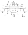
振動センサ1pにおける凸状部材40p及び/又はその基板10への接着剤は、図5に示すように、膨出面40b1側から大きな応力を受けた際に平坦面40aの平坦性を維持可能な材質で形成されていてもよい。平坦面40aの平坦性を維持可能な凸状部材40pの材質は、例えば、平坦性を維持可能な硬質性を有する金属、樹脂、ゴムなどであってもよい。平坦面40aの平坦性を維持可能な接着剤は、硬化性・耐衝撃性を有する樹脂などであってもよい。図5は、実施形態の第1の変形例にかかる振動センサ1pの動作を示す断面図である。このとき、図6(a)に示すように、基板10の表面10aにおいて、Z方向から透視した場合に凸状部材40pに重なる領域を凸部対応エリア(固着領域)10a1と呼び、その周囲の領域を凸部非対応エリア(非固着領域)10a2と呼ぶことにする。図6(b)に示すように、基板10の裏面10bにおいて、Z方向から透視した場合に凸状部材40pに重なる領域を凸部対応エリア(固着領域)10b1と呼び、その周囲の領域を凸部非対応エリア(非固着領域)10b2と呼ぶことにする。凸部対応エリア10b1は、凸状部材40pの平坦面40aが固着される固着領域である。凸部非対応エリア10b2は、凸状部材40pの平坦面40aが固着されない非固着領域である。
例えば、図5に示すように、基板10が他の部材100a,100bにより両持ち梁状に固定される場合、白抜きの矢印で示すように、対象物(例えば、人体の一部)から凸状部材40pが振動による力を受けると、その力が凸状部材40pから基板10へ伝達され、基板10が破線で示す位置から実線で示す位置へ変位して撓み得る。凸状部材40pが平坦面40aの平坦性を維持可能な材質で形成されているので、凸状部材40が凸部対応エリア10a1,10b1の湾曲を抑制してその平坦性を維持しながら凸部非対応エリア10a2,10b2をより大きな曲率で湾曲させ、基板10を効率的に撓ませることができる。すなわち、図5に示されるように、凸状部材40pに凸面40bの側(-Z側)から応力が加えられた際に、基板10は、接着剤の固化による硬さ、または凸状部材40pの平坦面40aの部分の硬さにより、凸部対応エリア(固着領域)10a2,10b2の平坦性が保持され、凸部対応エリア(固着領域)10a1,10b1と凸部非対応エリア(非固着領域)10a2,10b2とで湾曲の度合いが異なる。すなわち、基板10は、凸部非対応エリア10a2,10b2の方が凸部対応エリア10a1,10b1より湾曲性が大きくなる。凸部対応エリア10a1では、Z方向の撓みが抑制されつつXY方向の撓みが圧電素子20付近の領域に伝達され、凸部対応エリア10a1と凸部非対応エリア10a2との境界部分10cが支点となり、Z方向の撓みが凸部非対応エリア10a2で効率的に吸収される。これにより、凸部対応エリア10a1においてその平坦性を維持できるので、ハンダ等の導電性接合材のクラックを抑制でき、圧電素子20の信頼性を向上できる。それとともに、圧電素子20の極性がXY方向であり、凸部対応エリア10a1におけるXY方向の撓みで圧電体21を効率的に変位させることができるので、振動による力を圧電素子20で感度よく検知させることができる。すなわち、圧電素子20の信頼性向上と感度向上とを両立化できる。
また、圧電素子20以外の素子50は、図6(a)に示すように、凸部対応エリア10a1と凸部非対応エリア10a2との境界部分10cを避けて基板10の表面10aに配置されてもよい。素子50は、Z方向から透視した場合に、凸部対応エリア10a1内に含まれるように配置されてもよいし、凸部非対応エリア10a2に含まれるように配置されてもよい。図6(a)では、素子50が凸部対応エリア10a1内に含まれるように配置される構成が例示されている。これにより、素子50が境界部分10cを跨ぐように基板10の表面10aに配置される場合に比べて、素子50が配置される領域の平坦性を向上でき、素子50への応力を抑制できるので、ハンダ等の導電性接合材のクラックを抑制でき、素子50の信頼性を向上できる。
あるいは、振動センサ1iにおける凸状部材40iは、図7に示すように、基板10の裏面10bに対して実質的に点接触するように構成されていてもよい。図7は、実施形態の第2の変形例にかかる振動センサ1iの構成を示す断面図である。振動センサ1iは、凸状部材40(図1参照)に代えて凸状部材40iを有する。凸状部材40iは、棒状部材40cをさらに有する。棒状部材40cは、基板10の裏面10b側における圧電素子20に対応した位置に配されており、基板10の裏面10bと平坦面40aとの間に配されている。棒状部材40cの-Z側の端部は、平坦面40aに接触しており、平坦面40aに固定され得る。棒状部材40cの+Z側の端部は、基板10の裏面10bに接触しており、基板10の裏面10bに固定され得る。棒状部材40cの+Z側の端部は、導電膜30に接触しており、導電膜30に固定され得る。棒状部材40c+Z側の端部における裏面10bへの接触面積は、平坦面40aの面積より小さい。これにより、棒状部材40cが基板10の裏面10bに対して実質的に点接触すると見なすことができる。
図8に示すように、基板10が他の部材100a,100bにより両持ち梁状に固定される場合、白抜きの矢印で示すように、対象物(例えば、人体の一部)から凸状部材40iが振動による力を受けると、その力が凸状部材40iにおける棒状部材40cから基板10へ伝達され、基板10が破線で示す位置から実線で示す位置へ変位して撓み得る。図8は、振動センサ1iの動作を示す断面図である。このとき、凸状部材40iにおける棒状部材40cが基板10の裏面10bに実質的に点接触しているので、凸状部材40iが基板10をさらに効率的に撓ませることができる。これにより、圧電素子20における圧電体21をさらに効率的に変位させることができ、振動による力を圧電素子20でさらに感度よく検知させることができる。
あるいは、振動センサ1jは、対象物からの振動を伝達するための部材を圧電素子20の周囲に設ける必要がないことを利用して、圧電素子20の周囲に防水構造が設けられていてもよい。例えば、図9に示すように、振動センサ1jは、カバー60j、接着層70j、及び導電膜80jを有する。図9は、実施形態の第3の変形例にかかる振動センサ1jの構成を示す断面図である。カバー60jは、基板10の表面10a側に配され、表面10a側で圧電素子20を囲っている。カバー60jは、絶縁性樹脂等の外部の水分を遮断可能な任意の材料で形成され得る。カバー60jは、圧電素子20の側に開口した開口構造60aを有する。接着層70jは、カバー60jにおける開口構造60aの端部を基板10の表面10aにおける周縁部10a1へ封止する。これにより、カバー60j及び基板10で囲まれた空間を実質的に外部の空間から遮蔽でき、圧電素子20及び他の素子50を外部の水分から保護することができる。
また、導電膜80jをカバー60jにおける圧電素子20の側の面(すなわち、カバー60jの内面)を覆っている。導電膜80jは、金属(例えば、銅又はアルミニウム)を主成分とする材料で形成されてもよい。導電膜80jは、図9に波線で示すように、グランド電位に電気的に接続され得る。これにより、例えば、+Z側から電磁波ノイズが到来した際にその電磁波ノイズを導電膜80jで誘導電流等のノイズ電流に変換することができ、変換されたノイズ電流を導電膜80jからグランド電位に逃がすことができるので、圧電素子20、他の素子50、及びそれらの信号経路を電磁波ノイズからさらに確実にシールドできる。
あるいは、振動センサ1kにおいて、凸状部材及びカバーは、それぞれ、共通のケースの一部として一体成型されていてもよい。例えば、図10に示すように、振動センサ1kは、凸状部材40、カバー60j、及び導電膜80j(図9参照)に代えて、凸状部材140k、カバー160k、及び導電膜180kを含むケース110kを有する。図10は、ケース110kは、プラスチック等の樹脂成型可能な任意の材料で形成され得る。これにより、凸状部材140k、カバー160k、及び導電膜180kを低コストで構成できる。実施形態の第4の変形例にかかる振動センサ1kの構成を示す断面図である。
このとき、振動センサ1kは、図11に示すように製造されてもよい。図11(a)~図11(c)は、実施形態の第4の変形例にかかる振動センサ1kの製造方法を示す工程断面図である。
図11(a)に示す工程では、基板10の表面10aに圧電素子20及び他の素子50を実装するとともにその周縁部に接着剤を塗布して接着層70jを形成する。また、基板10の裏面10bにメッキ等により導電膜30を形成する。凸状部材140k及びカバー160kを含むケース110kを樹脂成型等により一体成型し、カバー160kの内面に相当する面にメッキ等により導電膜180kを形成する。
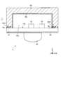
図11(b)及び図12に示す工程では、カバー160kの開口構造180a内に圧電素子20及び他の部品50が収容されるように基板10を上下逆にして設置し、接着層70jをケース110kに接触させ、接着層70jを介して基板10及びケース110kを互いに接着させる。
なお、ケース110kには、内側壁部110k1及び外側壁部110k2を含む嵌合構造が設けられている。内側壁部110k1は、図11(b)に示すように、XZ断面視において、基板10が接着される面の高さから-Z方向に立ち上がっている。内側壁部110k1は、図12に示すように、XY平面視において、Y方向に沿って延びた部分110k11と、部分110k11の-Y側の端部から-X方向に延びた部分110k12と、部分110k11の+Y側の端部から-X方向に延びた部分110k13とを有する。
外側壁部110k2は、図11(b)に示すように、XZ断面視において、凸状部材140kの-Z側の端部の高さから-Z方向に立ち上がっている。外側壁部110k2は、図12に示すように、XY平面視において、Y方向に沿って延びた部分110k21と、部分110k21の-Y側の端部から+X方向に延びた部分110k22と、部分110k21の+Y側の端部から+X方向に延びた部分110k23とを有する。
内側壁部110k1の外面のY方向幅は外側壁部110k2の内面のY方向幅に対応しており、内側壁部110k1及び外側壁部110k2は、互いに嵌合するように構成されている。
図11(c)に示す工程では、ケース110kを折れ線110k3で折り曲げて内側壁部110k1及び外側壁部110k2を互いに嵌合させ、ケース110k内への基板10の収容を完成させる。
このように、実施形態の第4の変形例では、簡易な工程で凸状部材140k、カバー160k、及び導電膜180kを製造できる。
あるいは、振動センサ1nにおいて、カバー60nは、嵌め込み式で構成されていてもよい。例えば、振動センサ1nは、図13に示すように、カバー60j及び導電膜80j(図9参照)に代えてカバー60n及び導電膜80nを有し、接着層70j(図9参照)を有さなくてもよい。図13は、実施形態の第5の変形例にかかる振動センサ1nの構成を示す断面図である。カバー60nは、基板10の+X側端部及び-X側端部がそれぞれ嵌め込まれるべき溝60n1をその開口構造60a’の内面に有する。開口構造60a’の内面において、溝60n1は、基板10が嵌め込まれた際に凸状部材40の最も-Z側に位置する部分がカバー60nの開口構造60a’の端部より-Z側に位置するように形成され得る。
このとき、振動センサ1nは、図14に示すように製造されてもよい。図14(a)~図14(b)は、実施形態の第5の変形例にかかる振動センサ1nの製造方法を示す工程断面図である。
図14(a)に示す工程では、基板10の表面10aに圧電素子20及び他の素子50を実装する。また、基板10の裏面10bにメッキ等により導電膜30を形成し、その上に凸状部材40を固定する。また、カバー60nの内面における圧電素子20の側となるべき領域にメッキ等により導電膜80nを形成する。
図14(b)に示す工程では、カバー60nの開口構造60a’内に圧電素子20及び他の部品50が収容される向きで基板10をカバー60nの溝60n-1に嵌め込み、カバー60n内への基板10の収容を完成させる。
このように、実施形態の第5の変形例では、さらに簡易な工程でカバー60n、及び導電膜80nを製造できる。
1,1i,1j,1k,1n 振動センサ
10 基板
20 圧電素子
30 導電膜
40,40i 凸状部材
50 素子
60j,60n カバー
70j 接着層
80j,80n 導電膜
110k ケース
140k 凸状部材
160k カバー
180k 導電膜
10 基板
20 圧電素子
30 導電膜
40,40i 凸状部材
50 素子
60j,60n カバー
70j 接着層
80j,80n 導電膜
110k ケース
140k 凸状部材
160k カバー
180k 導電膜
Claims (21)
- 第1主面と相対向する第2主面とを有し、第1主面側で片端又は両端が支持された基板と、
前記基板の第2主面に設けられた導電パターンと、
前記基板のほぼ中央で、前記第1主面に接着材により平坦面で固着された凸状部材と、
前記凸状部材が固着された第1領域内に位置し、前記導電パターンと電気的に接続されて前記第2主面に設けられた圧電素子と、
を備えた振動センサ。 - 平面視で矩形となり、第1主面と相対向する第2主面とを有し、第1主面側で1つの短辺または2つの短辺が支持された基板と、
前記基板の第2主面に設けられた導電パターンと、
前記基板のほぼ中央で、前記第1主面に接着材により平坦面で固着された凸状部材と、
前記凸状部材が固着された第1領域内に位置し、前記導電パターンと電気的に接続されて前記第2主面に設けられた圧電素子と、
を備えた振動センサ。 - 前記基板の第2主面に設けられ、前記導電パターンを介して前記圧電素子と電気的に接続されて設けられた素子とを有し、
前記素子は、前記第1領域または前記第1領域以外の第2領域に設けられる
請求項1または請求項2に記載の振動センサ。 - 前記接着材の固化による硬さ、または前記凸状部材の平坦面の部分の硬さにより、前記第1領域の平坦性が保持され、前記第1領域と前記第1領域以外の第2領域とで湾曲の度合いが異なる
請求項1から請求項3のいずれか1項に記載の振動センサ。 - 前記基板は、平面視で長方形となり、前記第1主面側で一方の短辺または2つの短辺が支持される、
請求項1から請求項4のいずれか1項に記載の振動センサ。 - 第1主面と前記第1主面の反対側に配された第2主面とを有する基板と、
前記第2主面に配された圧電素子と、
前記第1主面に配される導電膜と、
を備えた振動センサ。 - 前記基板に対して前記第1主面側に配された凸状部材をさらに備えた
請求項6に記載の振動センサ。 - 前記凸状部材の平面幅は、前記基板の平面幅より小さい
請求項7に記載の振動センサ。 - 前記凸状部材は、前記基板に対して前記第1主面側における前記圧電素子に対応した位置に配されている
請求項8に記載の振動センサ。 - 前記凸状部材は、
前記導電膜に接触している平坦面と、
前記平坦面の端部から前記導電膜に対して突出する凸面と、
を有する
請求項7から9のいずれか1項に記載の振動センサ。 - 前記第1主面は、前記第1主面に垂直な方向から透視した場合に前記凸状部材に重なる第1の固着領域と前記第1の固着領域の周囲に配された第1の非固着領域とを含み、
前記凸状部材は、前記第1の固着領域に固着剤で固着される平坦面を有し、
前記第2主面は、前記第2主面に垂直な方向から透視した場合に前記凸状部材に重なる第2の固着領域と前記第2の固着領域の周囲に配された第2の非固着領域とを含み、
前記圧電素子は、前記第2の固着領域に配されている
請求項7から9のいずれか1項に記載の振動センサ。 - 前記固着剤は、ろう材、導電ペーストまたは導電性樹脂である
請求項11に記載の振動センサ。 - 前記凸状部材は、前記平坦面の端部から前記導電膜に対して突出する凸面をさらに有し、
前記凸状部材に前記凸面の側から応力が加えられた際に、前記基板は、前記第1の非固着領域及び前記第2の非固着領域の方が前記第1の固着領域及び前記第2の固着領域より湾曲性が大きくなる
請求項11又は12に記載の振動センサ。 - 前記圧電素子に電気的に接続され、前記第2の固着領域内に又は前記第2の非固着領域内に配されている素子をさらに備えた
請求項11から13のいずれか1項に記載の振動センサ。 - 前記凸状部材は、
一端が前記導電膜に接触している棒状部材と、
前記棒状部材の他端が接続された平坦面と、
前記平坦面の端部から前記導電膜に対して突出する凸面と、
を有する
請求項7から9のいずれか1項に記載の振動センサ。 - 前記第1主面の側で前記圧電素子を囲うカバーをさらに備えた
請求項7から15のいずれか1項に記載の振動センサ。 - 前記カバーは、開口構造を有し、
前記振動センサは、前記開口構造の端部を前記基板の周縁部へ封止する接着層をさらに備えた
請求項16に記載の振動センサ。 - 前記カバーは、前記圧電素子の側の面が第2の導電膜で覆われる
請求項17に記載の振動センサ。 - 前記凸状部材及び前記カバーは、それぞれ、共通のケースの一部として一体成型されている
請求項16に記載の振動センサ。 - 前記凸状部材は、前記ケースにおける前記導電膜を覆う部分に対して突出する凸面を有する
請求項19に記載の振動センサ。 - 前記カバーは、前記基板の端部をスライド可能に収容する溝が形成された開口構造を有する
請求項16に記載の振動センサ。
Priority Applications (2)
| Application Number | Priority Date | Filing Date | Title |
|---|---|---|---|
| JP2020568647A JPWO2020158952A1 (ja) | 2019-01-31 | 2020-01-31 | 振動センサ |
| US17/390,172 US20210356318A1 (en) | 2019-01-31 | 2021-07-30 | Vibration sensor |
Applications Claiming Priority (2)
| Application Number | Priority Date | Filing Date | Title |
|---|---|---|---|
| JP2019016427 | 2019-01-31 | ||
| JP2019-016427 | 2019-01-31 |
Related Child Applications (1)
| Application Number | Title | Priority Date | Filing Date |
|---|---|---|---|
| US17/390,172 Continuation US20210356318A1 (en) | 2019-01-31 | 2021-07-30 | Vibration sensor |
Publications (1)
| Publication Number | Publication Date |
|---|---|
| WO2020158952A1 true WO2020158952A1 (ja) | 2020-08-06 |
Family
ID=71841042
Family Applications (1)
| Application Number | Title | Priority Date | Filing Date |
|---|---|---|---|
| PCT/JP2020/003828 Ceased WO2020158952A1 (ja) | 2019-01-31 | 2020-01-31 | 振動センサ |
Country Status (3)
| Country | Link |
|---|---|
| US (1) | US20210356318A1 (ja) |
| JP (1) | JPWO2020158952A1 (ja) |
| WO (1) | WO2020158952A1 (ja) |
Cited By (4)
| Publication number | Priority date | Publication date | Assignee | Title |
|---|---|---|---|---|
| JP2022182865A (ja) * | 2021-05-28 | 2022-12-08 | アルプスアルパイン株式会社 | 検出装置 |
| JP2023001820A (ja) * | 2021-06-21 | 2023-01-06 | 株式会社弘栄ドリームワークス | 押し当て部材および振動情報取得装置 |
| JP2023031624A (ja) * | 2021-08-25 | 2023-03-09 | 前田建設工業株式会社 | 振動センサ |
| JP2025037302A (ja) * | 2023-09-06 | 2025-03-18 | 株式会社村田製作所 | 電子機器 |
Citations (7)
| Publication number | Priority date | Publication date | Assignee | Title |
|---|---|---|---|---|
| JPH06201451A (ja) * | 1993-01-08 | 1994-07-19 | Fujikura Ltd | 圧電型振動センサ装置 |
| JPH0843430A (ja) * | 1994-07-28 | 1996-02-16 | Fujikura Ltd | 圧電型振動センサとその製法 |
| JPH08129071A (ja) * | 1994-11-02 | 1996-05-21 | Tokyo Gas Co Ltd | 地震動検出器およびsi値検出装置 |
| US20130144176A1 (en) * | 2010-06-25 | 2013-06-06 | Drexel University | Non-invasive blood pressure sensor |
| KR20170128654A (ko) * | 2016-05-12 | 2017-11-23 | (주) 센불 | 패치형 압전 변환기를 이용한 진동 센서노드 |
| JP2018149094A (ja) * | 2017-03-13 | 2018-09-27 | ヤマハ株式会社 | 生体振動センサー |
| JP2019010240A (ja) * | 2017-06-29 | 2019-01-24 | ヤマハ株式会社 | 振動センサ |
Family Cites Families (13)
| Publication number | Priority date | Publication date | Assignee | Title |
|---|---|---|---|---|
| US6491647B1 (en) * | 1998-09-23 | 2002-12-10 | Active Signal Technologies, Inc. | Physiological sensing device |
| KR100754507B1 (ko) * | 2005-11-30 | 2007-09-03 | (주)아이블포토닉스 | 맥파측정용 압전 센서 및 이를 이용한 맥파 측정 시스템 |
| US20070287923A1 (en) * | 2006-05-15 | 2007-12-13 | Charles Adkins | Wrist plethysmograph |
| CN201514275U (zh) * | 2009-10-10 | 2010-06-23 | 精量电子(深圳)有限公司 | 一种高灵敏度接触式振动监测压电传感器 |
| JP5590248B2 (ja) * | 2011-10-05 | 2014-09-17 | 株式会社村田製作所 | 超音波センサ |
| CN203232772U (zh) * | 2013-05-02 | 2013-10-09 | 群丰科技股份有限公司 | 电感元件 |
| JP2016024107A (ja) * | 2014-07-23 | 2016-02-08 | 日本電気株式会社 | 振動センサユニット |
| JP5798699B1 (ja) * | 2014-10-24 | 2015-10-21 | 太陽誘電株式会社 | 電気音響変換装置 |
| ITUB20159497A1 (it) * | 2015-12-24 | 2017-06-24 | St Microelectronics Srl | Dispositivo piezoelettrico mems e relativo procedimento di fabbricazione |
| CN109069029A (zh) * | 2016-04-28 | 2018-12-21 | 太阳诱电株式会社 | 振动波形传感器和脉搏波检测装置 |
| JP6742797B2 (ja) * | 2016-04-28 | 2020-08-19 | 太陽誘電株式会社 | 振動波形センサ |
| CN106361299B (zh) * | 2016-09-22 | 2023-03-24 | 安徽理工大学 | 一种三重薄膜心血管检测传感器 |
| CN207832310U (zh) * | 2018-02-06 | 2018-09-07 | 麒盛科技股份有限公司 | 一体式生理信号检测传感器 |
-
2020
- 2020-01-31 JP JP2020568647A patent/JPWO2020158952A1/ja active Pending
- 2020-01-31 WO PCT/JP2020/003828 patent/WO2020158952A1/ja not_active Ceased
-
2021
- 2021-07-30 US US17/390,172 patent/US20210356318A1/en not_active Abandoned
Patent Citations (7)
| Publication number | Priority date | Publication date | Assignee | Title |
|---|---|---|---|---|
| JPH06201451A (ja) * | 1993-01-08 | 1994-07-19 | Fujikura Ltd | 圧電型振動センサ装置 |
| JPH0843430A (ja) * | 1994-07-28 | 1996-02-16 | Fujikura Ltd | 圧電型振動センサとその製法 |
| JPH08129071A (ja) * | 1994-11-02 | 1996-05-21 | Tokyo Gas Co Ltd | 地震動検出器およびsi値検出装置 |
| US20130144176A1 (en) * | 2010-06-25 | 2013-06-06 | Drexel University | Non-invasive blood pressure sensor |
| KR20170128654A (ko) * | 2016-05-12 | 2017-11-23 | (주) 센불 | 패치형 압전 변환기를 이용한 진동 센서노드 |
| JP2018149094A (ja) * | 2017-03-13 | 2018-09-27 | ヤマハ株式会社 | 生体振動センサー |
| JP2019010240A (ja) * | 2017-06-29 | 2019-01-24 | ヤマハ株式会社 | 振動センサ |
Cited By (7)
| Publication number | Priority date | Publication date | Assignee | Title |
|---|---|---|---|---|
| JP2022182865A (ja) * | 2021-05-28 | 2022-12-08 | アルプスアルパイン株式会社 | 検出装置 |
| JP7655786B2 (ja) | 2021-05-28 | 2025-04-02 | アルプスアルパイン株式会社 | 検出装置 |
| JP2023001820A (ja) * | 2021-06-21 | 2023-01-06 | 株式会社弘栄ドリームワークス | 押し当て部材および振動情報取得装置 |
| JP7748083B2 (ja) | 2021-06-21 | 2025-10-02 | 株式会社弘栄ドリームワークス | 押し当て部材および振動情報取得装置 |
| JP2023031624A (ja) * | 2021-08-25 | 2023-03-09 | 前田建設工業株式会社 | 振動センサ |
| JP7687905B2 (ja) | 2021-08-25 | 2025-06-03 | 前田建設工業株式会社 | 振動センサ |
| JP2025037302A (ja) * | 2023-09-06 | 2025-03-18 | 株式会社村田製作所 | 電子機器 |
Also Published As
| Publication number | Publication date |
|---|---|
| US20210356318A1 (en) | 2021-11-18 |
| JPWO2020158952A1 (ja) | 2021-12-02 |
Similar Documents
| Publication | Publication Date | Title |
|---|---|---|
| WO2020158952A1 (ja) | 振動センサ | |
| CN102901493B (zh) | 振动器件以及电子设备 | |
| US8551003B2 (en) | Ultrasonic probe and ultrasonic diagnosis device | |
| JP5487672B2 (ja) | 物理量センサ | |
| US20100179430A1 (en) | Ultrasonic probe and method for manufacturing the same and ultrasonic diagnostic device | |
| CN107249763B (zh) | 包括多个单换能器的声换能器和用于其制造的方法 | |
| US10848123B2 (en) | Vibration device | |
| JP2012193971A (ja) | センサーモジュール、センサーデバイス、センサーデバイスの製造方法及び電子機器 | |
| JP5590248B2 (ja) | 超音波センサ | |
| CN111384134B (zh) | 显示装置 | |
| US11650054B2 (en) | Vibrator device, electronic apparatus, and vehicle | |
| CN112448690B (zh) | 振动器件 | |
| CN106206927A (zh) | 压电体、振动波马达和电子设备 | |
| WO2021191948A1 (ja) | 振動測定用基板モジュール及び振動検出装置 | |
| CN107409262B (zh) | 超声波传感器 | |
| JP2013137330A (ja) | 圧電式加速度センサ | |
| JP2020128899A (ja) | 振動センサ | |
| JP2010044005A (ja) | 圧電振動子、圧電デバイス | |
| US20250024755A1 (en) | Ultrasonic transducer and method of manufacturing the same | |
| JPWO2021186860A5 (ja) | ||
| JP7343048B2 (ja) | 加速度検出装置 | |
| US11114995B2 (en) | Piezoelectric component | |
| JP2019125968A (ja) | 車載用超音波センサ | |
| JP2010199889A (ja) | コンデンサマイクロホン | |
| JP5270622B2 (ja) | 圧電式加速度センサ |
Legal Events
| Date | Code | Title | Description |
|---|---|---|---|
| 121 | Ep: the epo has been informed by wipo that ep was designated in this application |
Ref document number: 20749092 Country of ref document: EP Kind code of ref document: A1 |
|
| ENP | Entry into the national phase |
Ref document number: 2020568647 Country of ref document: JP Kind code of ref document: A |
|
| NENP | Non-entry into the national phase |
Ref country code: DE |
|
| 122 | Ep: pct application non-entry in european phase |
Ref document number: 20749092 Country of ref document: EP Kind code of ref document: A1 |