WO2020158507A1 - Dispersion liquid, conductive film and method for producing same, electrode, and solar cell - Google Patents
Dispersion liquid, conductive film and method for producing same, electrode, and solar cell Download PDFInfo
- Publication number
- WO2020158507A1 WO2020158507A1 PCT/JP2020/001921 JP2020001921W WO2020158507A1 WO 2020158507 A1 WO2020158507 A1 WO 2020158507A1 JP 2020001921 W JP2020001921 W JP 2020001921W WO 2020158507 A1 WO2020158507 A1 WO 2020158507A1
- Authority
- WO
- WIPO (PCT)
- Prior art keywords
- conductive film
- condensate
- less
- solar cell
- dispersion
- Prior art date
Links
Images

Classifications
-
- C—CHEMISTRY; METALLURGY
- C08—ORGANIC MACROMOLECULAR COMPOUNDS; THEIR PREPARATION OR CHEMICAL WORKING-UP; COMPOSITIONS BASED THEREON
- C08L—COMPOSITIONS OF MACROMOLECULAR COMPOUNDS
- C08L61/00—Compositions of condensation polymers of aldehydes or ketones; Compositions of derivatives of such polymers
- C08L61/04—Condensation polymers of aldehydes or ketones with phenols only
- C08L61/06—Condensation polymers of aldehydes or ketones with phenols only of aldehydes with phenols
- C08L61/14—Modified phenol-aldehyde condensates
-
- C—CHEMISTRY; METALLURGY
- C08—ORGANIC MACROMOLECULAR COMPOUNDS; THEIR PREPARATION OR CHEMICAL WORKING-UP; COMPOSITIONS BASED THEREON
- C08G—MACROMOLECULAR COMPOUNDS OBTAINED OTHERWISE THAN BY REACTIONS ONLY INVOLVING UNSATURATED CARBON-TO-CARBON BONDS
- C08G8/00—Condensation polymers of aldehydes or ketones with phenols only
- C08G8/04—Condensation polymers of aldehydes or ketones with phenols only of aldehydes
- C08G8/08—Condensation polymers of aldehydes or ketones with phenols only of aldehydes of formaldehyde, e.g. of formaldehyde formed in situ
- C08G8/18—Condensation polymers of aldehydes or ketones with phenols only of aldehydes of formaldehyde, e.g. of formaldehyde formed in situ with phenols substituted by carboxylic or sulfonic acid groups
-
- C—CHEMISTRY; METALLURGY
- C08—ORGANIC MACROMOLECULAR COMPOUNDS; THEIR PREPARATION OR CHEMICAL WORKING-UP; COMPOSITIONS BASED THEREON
- C08G—MACROMOLECULAR COMPOUNDS OBTAINED OTHERWISE THAN BY REACTIONS ONLY INVOLVING UNSATURATED CARBON-TO-CARBON BONDS
- C08G8/00—Condensation polymers of aldehydes or ketones with phenols only
- C08G8/04—Condensation polymers of aldehydes or ketones with phenols only of aldehydes
- C08G8/08—Condensation polymers of aldehydes or ketones with phenols only of aldehydes of formaldehyde, e.g. of formaldehyde formed in situ
- C08G8/24—Condensation polymers of aldehydes or ketones with phenols only of aldehydes of formaldehyde, e.g. of formaldehyde formed in situ with mixtures of two or more phenols which are not covered by only one of the groups C08G8/10 - C08G8/20
-
- C—CHEMISTRY; METALLURGY
- C08—ORGANIC MACROMOLECULAR COMPOUNDS; THEIR PREPARATION OR CHEMICAL WORKING-UP; COMPOSITIONS BASED THEREON
- C08J—WORKING-UP; GENERAL PROCESSES OF COMPOUNDING; AFTER-TREATMENT NOT COVERED BY SUBCLASSES C08B, C08C, C08F, C08G or C08H
- C08J5/00—Manufacture of articles or shaped materials containing macromolecular substances
- C08J5/18—Manufacture of films or sheets
-
- C—CHEMISTRY; METALLURGY
- C08—ORGANIC MACROMOLECULAR COMPOUNDS; THEIR PREPARATION OR CHEMICAL WORKING-UP; COMPOSITIONS BASED THEREON
- C08K—Use of inorganic or non-macromolecular organic substances as compounding ingredients
- C08K3/00—Use of inorganic substances as compounding ingredients
- C08K3/02—Elements
- C08K3/04—Carbon
- C08K3/046—Carbon nanorods, nanowires, nanoplatelets or nanofibres
-
- C—CHEMISTRY; METALLURGY
- C08—ORGANIC MACROMOLECULAR COMPOUNDS; THEIR PREPARATION OR CHEMICAL WORKING-UP; COMPOSITIONS BASED THEREON
- C08L—COMPOSITIONS OF MACROMOLECULAR COMPOUNDS
- C08L61/00—Compositions of condensation polymers of aldehydes or ketones; Compositions of derivatives of such polymers
- C08L61/04—Condensation polymers of aldehydes or ketones with phenols only
- C08L61/06—Condensation polymers of aldehydes or ketones with phenols only of aldehydes with phenols
-
- C—CHEMISTRY; METALLURGY
- C09—DYES; PAINTS; POLISHES; NATURAL RESINS; ADHESIVES; COMPOSITIONS NOT OTHERWISE PROVIDED FOR; APPLICATIONS OF MATERIALS NOT OTHERWISE PROVIDED FOR
- C09D—COATING COMPOSITIONS, e.g. PAINTS, VARNISHES OR LACQUERS; FILLING PASTES; CHEMICAL PAINT OR INK REMOVERS; INKS; CORRECTING FLUIDS; WOODSTAINS; PASTES OR SOLIDS FOR COLOURING OR PRINTING; USE OF MATERIALS THEREFOR
- C09D161/00—Coating compositions based on condensation polymers of aldehydes or ketones; Coating compositions based on derivatives of such polymers
- C09D161/04—Condensation polymers of aldehydes or ketones with phenols only
- C09D161/06—Condensation polymers of aldehydes or ketones with phenols only of aldehydes with phenols
- C09D161/14—Modified phenol-aldehyde condensates
-
- H—ELECTRICITY
- H01—ELECTRIC ELEMENTS
- H01B—CABLES; CONDUCTORS; INSULATORS; SELECTION OF MATERIALS FOR THEIR CONDUCTIVE, INSULATING OR DIELECTRIC PROPERTIES
- H01B1/00—Conductors or conductive bodies characterised by the conductive materials; Selection of materials as conductors
- H01B1/04—Conductors or conductive bodies characterised by the conductive materials; Selection of materials as conductors mainly consisting of carbon-silicon compounds, carbon or silicon
-
- H—ELECTRICITY
- H01—ELECTRIC ELEMENTS
- H01B—CABLES; CONDUCTORS; INSULATORS; SELECTION OF MATERIALS FOR THEIR CONDUCTIVE, INSULATING OR DIELECTRIC PROPERTIES
- H01B1/00—Conductors or conductive bodies characterised by the conductive materials; Selection of materials as conductors
- H01B1/20—Conductive material dispersed in non-conductive organic material
- H01B1/24—Conductive material dispersed in non-conductive organic material the conductive material comprising carbon-silicon compounds, carbon or silicon
-
- H—ELECTRICITY
- H01—ELECTRIC ELEMENTS
- H01B—CABLES; CONDUCTORS; INSULATORS; SELECTION OF MATERIALS FOR THEIR CONDUCTIVE, INSULATING OR DIELECTRIC PROPERTIES
- H01B13/00—Apparatus or processes specially adapted for manufacturing conductors or cables
- H01B13/0036—Details
-
- H—ELECTRICITY
- H10—SEMICONDUCTOR DEVICES; ELECTRIC SOLID-STATE DEVICES NOT OTHERWISE PROVIDED FOR
- H10K—ORGANIC ELECTRIC SOLID-STATE DEVICES
- H10K85/00—Organic materials used in the body or electrodes of devices covered by this subclass
- H10K85/10—Organic polymers or oligomers
-
- C—CHEMISTRY; METALLURGY
- C08—ORGANIC MACROMOLECULAR COMPOUNDS; THEIR PREPARATION OR CHEMICAL WORKING-UP; COMPOSITIONS BASED THEREON
- C08J—WORKING-UP; GENERAL PROCESSES OF COMPOUNDING; AFTER-TREATMENT NOT COVERED BY SUBCLASSES C08B, C08C, C08F, C08G or C08H
- C08J2361/00—Characterised by the use of condensation polymers of aldehydes or ketones; Derivatives of such polymers
- C08J2361/04—Condensation polymers of aldehydes or ketones with phenols only
- C08J2361/06—Condensation polymers of aldehydes or ketones with phenols only of aldehydes with phenols
- C08J2361/08—Condensation polymers of aldehydes or ketones with phenols only of aldehydes with phenols with monohydric phenols
- C08J2361/10—Phenol-formaldehyde condensates
-
- C—CHEMISTRY; METALLURGY
- C08—ORGANIC MACROMOLECULAR COMPOUNDS; THEIR PREPARATION OR CHEMICAL WORKING-UP; COMPOSITIONS BASED THEREON
- C08K—Use of inorganic or non-macromolecular organic substances as compounding ingredients
- C08K2201/00—Specific properties of additives
- C08K2201/011—Nanostructured additives
-
- C—CHEMISTRY; METALLURGY
- C08—ORGANIC MACROMOLECULAR COMPOUNDS; THEIR PREPARATION OR CHEMICAL WORKING-UP; COMPOSITIONS BASED THEREON
- C08K—Use of inorganic or non-macromolecular organic substances as compounding ingredients
- C08K3/00—Use of inorganic substances as compounding ingredients
- C08K3/02—Elements
- C08K3/04—Carbon
- C08K3/041—Carbon nanotubes
-
- C—CHEMISTRY; METALLURGY
- C08—ORGANIC MACROMOLECULAR COMPOUNDS; THEIR PREPARATION OR CHEMICAL WORKING-UP; COMPOSITIONS BASED THEREON
- C08K—Use of inorganic or non-macromolecular organic substances as compounding ingredients
- C08K7/00—Use of ingredients characterised by shape
- C08K7/02—Fibres or whiskers
- C08K7/04—Fibres or whiskers inorganic
- C08K7/06—Elements
-
- Y—GENERAL TAGGING OF NEW TECHNOLOGICAL DEVELOPMENTS; GENERAL TAGGING OF CROSS-SECTIONAL TECHNOLOGIES SPANNING OVER SEVERAL SECTIONS OF THE IPC; TECHNICAL SUBJECTS COVERED BY FORMER USPC CROSS-REFERENCE ART COLLECTIONS [XRACs] AND DIGESTS
- Y02—TECHNOLOGIES OR APPLICATIONS FOR MITIGATION OR ADAPTATION AGAINST CLIMATE CHANGE
- Y02E—REDUCTION OF GREENHOUSE GAS [GHG] EMISSIONS, RELATED TO ENERGY GENERATION, TRANSMISSION OR DISTRIBUTION
- Y02E10/00—Energy generation through renewable energy sources
- Y02E10/50—Photovoltaic [PV] energy
- Y02E10/549—Organic PV cells
Definitions
- the present invention relates to a dispersion, a conductive film and a method for manufacturing the same, an electrode, and a solar cell, and particularly to a dispersion, a conductive film obtained by using the dispersion and a method for manufacturing the same, an electrode including the conductive film, and , A solar cell provided with the electrode.
- Carbon nanotubes (hereinafter sometimes referred to as “CNTs”), which is one of the carbon materials, are excellent in various properties such as electrical conductivity, thermal conductivity, mechanical strength, etc. Applications are under consideration. For example, a technique for forming a conductive film with CNT has been conventionally studied, paying attention to its excellent conductivity.
- the conductive film containing CNTs is obtained by, for example, applying a carbon nanotube dispersion liquid (hereinafter, also referred to as “CNT dispersion liquid”) containing CNTs, a solvent, and a dispersant onto a base material, and then drying it. , Can be formed on a substrate. Then, in order to improve the performance of such a conductive film or a conductive film having a conductive film on a base material, attempts have been made to improve the dispersant used and the CNT dispersion liquid.
- CNT dispersion liquid carbon nanotube dispersion liquid
- Patent Document 1 a transparent conductive film including a conductive film made of CNT and an aromatic polymer as a dispersant, and a layer made of a resin layer on the conductive film, and having a specific light transmittance and surface resistivity, is provided. It has been reported that the conductive film has high durability, high conductivity, and excellent light transmittance.
- an aqueous CNT dispersion liquid containing a dispersant having a number average molecular weight of 10,000 or more and 150,000 or less, such as a polysaccharide, at a specific ratio with respect to CNTs and having a pH adjusted within a specific range has been reported that while maintaining high dispersibility, it is excellent in stability against high shearing force.
- Patent Document 3 a styrenesulfonic acid monomer residue, a maleimide residue having a substituted or unsubstituted aromatic hydrocarbon group on the nitrogen atom, and itaconic acid and fumaric acid each represented by a specific structural formula.
- Polystyrene sulfonic acid copolymer containing another vinyl monomer residue derived from an acid or the like as a repeating structural unit, and the content ratio of each residue is 30 to 95 mol %, 5 to 70 mol %, and 0 to 20 mol %.
- Patent Document 4 when dispersing CNT in a solvent, a sulfonic acid group-containing monomer unit is contained as a dispersant, and an ethylenically unsaturated aliphatic carboxylic acid monomer unit is contained in a specific ratio.
- a polymer dispersant made of a polymer while suppressing the aggregation of CNTs in a CNT dispersion, it is possible to improve the adhesion between a conductive film formed using the dispersion and a substrate. It has been reported that it is possible.
- a dispersion liquid such as a CNT dispersion liquid is required to have coating properties (wettability) with respect to a base material.
- the conductive film formed from the dispersion liquid is required to have conductivity and excellent adhesion to the substrate. Further, for example, when the conductive film is used as a counter electrode of a dye-sensitized solar cell, excellent catalytic activity is required. In addition, a solar cell manufactured using a conductive film is required to have high conversion efficiency.
- the coating property (wettability) of the dispersion liquid to the substrate and/or the adhesion between the conductive film formed from the dispersion liquid and the substrate are still insufficient. Therefore, there is room for improvement in the above-mentioned conventional technique in that the coating property (wettability) of the dispersion liquid with respect to the base material is improved while the adhesion of the conductive film formed from the dispersion liquid with the base material is improved. was there.
- an object of the present invention is to provide a dispersion liquid capable of improving the coating property (wettability) with respect to a base material and forming a conductive film having high adhesion to the base material.
- Another object of the present invention is to provide the conductive film, an electrode including the conductive film, and a solar cell including the electrode.
- the dispersion liquid contains a carbon material (A), a condensate (B) of an aromatic sulfonic acid compound, a hydroxyphenol compound and an aldehyde compound, and a solvent (C), and The inventors have found that it is possible to improve the coating property (wettability) with respect to, and to form a conductive film having high adhesion to a substrate, and completed the present invention.
- the present invention has an object to advantageously solve the above-mentioned problems, and the dispersion of the present invention comprises a carbon material (A), a condensation of an aromatic sulfonic acid compound, a hydroxyphenol compound and an aldehyde compound.
- the product (B) and the solvent (C) are included.
- the coating property (wettability) with respect to the substrate is improved.
- a conductive film that can be improved and has high adhesion to a base material can be formed.
- aromatic sulfonic acid compound means “a compound in which any one of hydrogen atoms in the aromatic compound is replaced with —SO 3 X (X is a hydrogen atom or a cation)”
- Hydrophenol compound means “a compound having at least one hydroxy group (hydroxyl group)” and other than “aromatic sulfonic acid compound”.
- the dispersion of the present invention comprises a hydroxyphenol compound monomer unit derived from a hydroxyphenol compound relative to an aromatic sulfonic acid compound monomer unit derived from an aromatic sulfonic acid compound in the condensate (B).
- the molar ratio (hydroxyphenol compound monomer unit/aromatic sulfonic acid compound monomer unit) is preferably 1/9 or more and 9/1 or less.
- the dispersibility of the condensate (B) can be improved.
- a conductive film having high adhesion to the base material can be efficiently formed.
- the dispersion of the present invention preferably has a weight average molecular weight (converted to standard polyethylene glycol) of the condensate (B) of 500 or more and 100,000 or less.
- the weight average molecular weight (converted to standard polyethylene glycol) of the condensate (B) is 500 or more and 100,000 or less, the dispersibility of the carbon material can be improved and the coating property (wettability) on the substrate can be improved. it can.
- a conductive film having high adhesion to the substrate can be efficiently formed, and a conductive film having improved conductivity, film strength, and catalytic activity when used as an electrode can be obtained.
- a solar cell manufactured using this conductive film has high conversion efficiency.
- the condensate (B) is preferably a resol type.
- the condensate (B) is preferably represented by the following general formula (1) or the following general formula (2).
- X represents a hydrogen atom or a cation
- R 1 represents a hydroxyl group, —CH 2 —OH , or a group represented by the following general formula (3)
- m, n, o and p are each an integer of 1 or more.
- l is an integer of 0 to 4
- Q is a divalent organic group
- R 2 is a hydroxyl group, —CH 2 —OH, or a hydrogen atom.
- Q in the general formula (3) is preferably a sulfonyl group.
- the carbon material (A) is preferably a fibrous carbon nanostructure.
- the solvent (C) contains water and the pH of the dispersion liquid is less than 7.
- the dispersion of the present invention preferably contains 50 parts by mass or more and 500 parts by mass or less of the condensate (B) per 100 parts by mass of the carbon material (A).
- the present invention has an object to advantageously solve the above problems, and the conductive film of the present invention is characterized by being obtained by using any one of the above-mentioned dispersion liquids.
- the dispersion liquid of the present invention it is possible to provide a conductive film having excellent adhesion to a substrate.
- an electrode of the present invention is characterized by including the above-mentioned conductive film.
- the electrode provided with the conductive film of the present invention has excellent conductivity.
- the present invention is intended to advantageously solve the above problems, and a solar cell of the present invention is characterized by including the above-mentioned electrode.
- the solar cell provided with the electrode of the present invention has high conversion efficiency.
- the present invention is intended to advantageously solve the above problems, the method for producing a conductive film of the present invention, any one of the above dispersion is applied to the substrate and dried to conduct A step (1) of forming a film, a step (2) of washing the conductive film obtained in the step (1) with a solvent to remove at least a part of the condensate (B) from the conductive film, It is characterized by including.
- INDUSTRIAL APPLICABILITY The conductive film manufacturing method of the present invention can efficiently manufacture a conductive film having excellent adhesion to a substrate.
- a dispersion liquid capable of improving the coating property (wettability) with respect to a substrate and forming a conductive film having high adhesion to the substrate.
- a conductive film having high adhesion to a base material a method for producing the conductive film, an electrode having the conductive film and having high conductivity, and a solar cell having the electrode and having high conversion efficiency. Can be provided.
- the carbon material dispersion liquid of the present invention contains the carbon material (A), the condensate (B), and the solvent (C), and further contains any other component as necessary.
- the dispersion of the present invention is preferably acidic.
- the dispersion liquid is acidic, when the dispersion liquid is applied on the conductive layer formed on the substrate, the conductive layer formed on the substrate and the dispersion liquid are eroded by the erosion of the conductive layer formed on the substrate. It is possible to improve the adhesion to the conductive layer.
- the carbon material (A) is not particularly limited, and has conductivity, fibrous carbon nanostructure, graphene, fullerene, carbon nanohorn, graphite, activated carbon, carbon fiber, porous carbon, expanded graphite, carbon particles.
- carbon black such as Ketjen black and acetylene black
- the fibrous carbon nanostructure is preferable in that the conductive film obtained has excellent strength and catalytic performance.
- the fibrous carbon nanostructure include a structure formed by stacking conical structures such as cup-stacked carbon nanotubes, and a cylindrical shape such as carbon nanobats and carbon nanotubes (CNTs).
- a carbon nanostructure such as a carbon nanostructure or a non-cylindrical carbon nanostructure such as a graphene nanoribbon formed by forming a carbon six-membered ring network in a flat tubular shape can be used. These may be used alone or in combination of two or more.
- a fibrous carbon nanostructure containing CNT as the fibrous carbon nanostructure.
- the fibrous carbon nanostructure may be made of CNT only. If a fibrous carbon nanostructure containing CNTs is used, even if the compounding amount is small, the obtained conductive film can have properties such as conductivity, film strength, and catalytic activity when used for a solar cell electrode. This is because it can be efficiently given.
- CNTs in the fibrous carbon nanostructure are not particularly limited, and single-walled carbon nanotubes and/or multi-walled carbon nanotubes can be used.
- the CNTs are preferably single-walled to five-walled carbon nanotubes, and more preferably single-walled carbon nanotubes. These may be used alone or in combination of two or more.
- the average diameter of the fibrous carbon nanostructures is preferably 1 nm or more, preferably 60 nm or less, more preferably 30 nm or less, and particularly preferably 10 nm or less.
- the average diameter of the fibrous carbon nanostructures is 1 nm or more, the dispersibility of the fibrous carbon nanostructures can be enhanced and the conductive film can be stably imparted with favorable characteristics such as conductivity.
- the average diameter of the fibrous carbon nanostructures is 60 nm or less, even if the compounding amount is small, the obtained conductive film can efficiently exhibit characteristics such as catalytic activity when used in a solar cell electrode. Can be given to.
- the “average diameter of fibrous carbon nanostructures” is, for example, the diameter (outer diameter) of 20 fibrous carbon nanostructures measured on a transmission electron microscope (TEM) image. , Can be obtained by calculating the number average value.
- the fibrous carbon nanostructure the ratio (3 ⁇ /Av) of the value (3 ⁇ ) obtained by multiplying the standard deviation ( ⁇ : sample standard deviation) of the diameter by 3 with respect to the average diameter (Av) is more than 0.20.
- a fibrous carbon nanostructure of less than 0.60 is preferably used, and a fibrous carbon nanostructure of 3 ⁇ /Av of more than 0.25 is more preferably used, and a fibrous carbon of 3 ⁇ /Av of more than 0.40 is used. It is particularly preferred to use carbon nanostructures.
- the use of the fibrous carbon nanostructure having 3 ⁇ /Av of more than 0.20 and less than 0.60 can further improve the performance of the produced conductive film.
- the average diameter (Av) and standard deviation ( ⁇ ) of the fibrous carbon nanostructure may be adjusted by changing the production method or production conditions of the fibrous carbon nanostructure, or obtained by a different production method.
- the fibrous carbon nanostructure may be adjusted by combining a plurality of types.
- the fibrous carbon nanostructure it is usually used that the diameter measured as described above is plotted on the abscissa and the frequency is plotted on the ordinate, and a normal distribution is obtained when approximated by Gaussian. To be done.
- the average length of the fibrous carbon nanostructure is preferably 10 ⁇ m or more, more preferably 50 ⁇ m or more, particularly preferably 80 ⁇ m or more, and preferably 600 ⁇ m or less, 500 ⁇ m It is more preferably not more than 400 ⁇ m, particularly preferably not more than 400 ⁇ m.
- the average length is 10 ⁇ m or more, a conductive path can be formed in the conductive film with a small amount and the strength of the conductive film is high.
- the average length is 600 ⁇ m or less, the coating property on the base material can be improved when the dispersion liquid is coated.
- the average length of the fibrous carbon nanostructures is, for example, the length of 20 fibrous carbon nanostructures measured on a scanning electron microscope (SEM) image. It can be obtained by calculating the average value.
- the fibrous carbon nanostructure usually has an aspect ratio of more than 10.
- the aspect ratio of the fibrous carbon nanostructures was determined by measuring the diameter and length of 100 randomly selected fibrous carbon nanostructures using a scanning electron microscope or a transmission electron microscope. It can be determined by calculating the average value of the ratio to the length (length/diameter).
- the fibrous carbon nanostructure has a BET specific surface area of preferably 200 m 2 /g or more, more preferably 400 m 2 /g or more, particularly preferably 600 m 2 /g or more, It is preferably 2000 m 2 /g or less, more preferably 1800 m 2 /g or less, and particularly preferably 1600 m 2 /g or less.
- the BET specific surface area of the fibrous carbon nanostructures is 200 m 2 /g or more, the dispersibility of the fibrous carbon nanostructures is increased, and the conductive film and the solar cell with respect to the conductive film obtained can be obtained with a small amount. It is possible to satisfactorily impart characteristics such as catalytic activity when used as a working electrode.
- BET specific surface area of the fibrous carbon nanostructure is 2000 m 2 /g or less
- the obtained conductive film is satisfactorily imparted with properties such as conductivity and catalytic activity when used as a solar cell electrode.
- the coating property of the dispersion liquid can be stabilized.
- BET specific surface area refers to the nitrogen adsorption specific surface area measured using the BET method.
- the fibrous carbon nanostructure preferably has a t-plot obtained from the adsorption isotherm showing a convex shape.
- the “t-plot” is obtained by converting the relative pressure into the average thickness t (nm) of the nitrogen gas adsorption layer in the adsorption isotherm of the fibrous carbon nanostructure measured by the nitrogen gas adsorption method. You can That is, from the known standard isotherm obtained by plotting the average thickness t of the nitrogen gas adsorption layer against the relative pressure P/P0, obtain the average thickness t of the nitrogen gas adsorption layer corresponding to the relative pressure and perform the above conversion. Gives a t-plot of the fibrous carbon nanostructure (t-plot method by de Boer et al.).
- the t-plot showing the upward convex shape is located on a straight line passing through the origin in the region where the average thickness t of the nitrogen gas adsorption layer is small, whereas when t becomes large, the plot becomes the straight line. The position is shifted downward from.
- the fibrous carbon nanostructure having the shape of the t-plot has a large ratio of the internal specific surface area to the total specific surface area of the fibrous carbon nanostructure, and many carbon nanostructures constituting the fibrous carbon nanostructure. Indicates that an opening is formed.
- the bending point of the t-plot of the fibrous carbon nanostructure is preferably in the range of 0.2 ⁇ t(nm) ⁇ 1.5, and 0.45 ⁇ t(nm) ⁇ 1.5. Is more preferable, and 0.55 ⁇ t(nm) ⁇ 1.0 is particularly preferable.
- the inflection point of the t-plot of the fibrous carbon nanostructure is within such a range, the dispersibility of the fibrous carbon nanostructure can be enhanced, and the properties such as conductivity of the conductive film can be enhanced with a small amount of compounding. ..
- the fibrous carbon nanostructures are likely to aggregate and the dispersibility decreases, and if the value of the bending point exceeds 1.5, the fibrous carbon nanostructure is formed.
- the structures may be easily entangled with each other and the dispersibility may be reduced.
- the "position of the bending point" is the intersection of the approximate straight line A in the above process (1) and the approximate straight line B in the above process (3).
- the ratio (S2/S1) of the internal specific surface area S2 to the total specific surface area S1 obtained from the t-plot is preferably 0.05 or more and 0.30 or less.
- the dispersibility of the fibrous carbon nanostructure can be enhanced and the properties such as the conductivity of the conductive film can be enhanced with a small blending amount.
- the total specific surface area S1 and the internal specific surface area S2 of the fibrous carbon nanostructure can be obtained from its t-plot.
- the total specific surface area S1 can be obtained from the slope of the approximate straight line in the process (1), and the external specific surface area S3 can be obtained from the slope of the approximate straight line in the process (3). Then, the internal specific surface area S2 can be calculated by subtracting the external specific surface area S3 from the total specific surface area S1.
- the measurement of the adsorption isotherm of the fibrous carbon nanostructure, the preparation of the t-plot, and the calculation of the total specific surface area S1 and the internal specific surface area S2 based on the analysis of the t-plot are carried out by using, for example, a commercially available measuring device.
- "BELSORP (registered trademark)-mini” manufactured by Nippon Bell Co., Ltd.
- the fibrous carbon nanostructure containing CNT suitable as the fibrous carbon nanostructure has a peak of Radial Breathing Mode (RBM) when evaluated using Raman spectroscopy. It should be noted that RBM does not exist in the Raman spectrum of the fibrous carbon nanostructure composed of only multi-walled carbon nanotubes having three or more layers.
- the ratio of the G band peak intensity to the D band peak intensity (G/D ratio) in the Raman spectrum is preferably 0.5 or more and 10.0 or less, and 1 It is more preferably from 0.0 to 5.0.
- G/D ratio is 0.5 or more and 10.0 or less, characteristics such as catalytic activity when used for a solar cell electrode can be favorably imparted to the obtained conductive film.
- the fibrous carbon nanostructure containing CNTs preferably has an oxygen atom amount of 5 atom% or less, and preferably 2 atom% or less, based on the total of carbon atoms and oxygen atoms by XPS elemental analysis. More preferably, it is particularly preferably 1 atomic% or less. When the amount of oxygen atoms is within the preferable range, it is possible to favorably provide the obtained conductive film with properties such as catalytic activity when used in a solar cell electrode.
- the proportion of carbon atoms is preferably 85% by mass or more, more preferably 90% by mass or more, and 95% by mass or more by elemental analysis of CHN. More preferably, it is particularly preferably 98 mass% or more, the proportion of hydrogen atoms is preferably 1 mass% or less, more preferably 0.8 mass% or less, 0.3 mass% The content is more preferably the following or less, and particularly preferably 0.1% by mass or less.
- the ratio of carbon atoms (hydrogen atoms) is within the preferable range, it is possible to satisfactorily provide the obtained conductive film with properties such as catalytic activity when used for a solar cell electrode.
- the fibrous carbon nanostructure containing CNTs is not particularly limited, and is manufactured using a known CNT synthesis method such as an arc discharge method, a laser ablation method, or a chemical vapor deposition method (CVD method). can do.
- a fibrous carbon nanostructure containing CNTs is prepared by, for example, supplying a raw material compound and a carrier gas onto a base material having a catalyst layer for producing carbon nanotubes on the surface thereof and performing chemical vapor deposition (CVD). Method), by which a small amount of an oxidizing agent (catalyst activating substance) is present in the system when CNTs are synthesized by the method (super growth method; WO 2006). /011655), and can be efficiently produced.
- the carbon nanotube obtained by the super growth method may be referred to as “SGCNT”.
- the fibrous carbon nanostructure manufactured by the super growth method may be composed of only SGCNT, or in addition to SGCNT, for example, another carbon nanostructure such as a non-cylindrical carbon nanostructure. May be included.
- the content of the carbon material (A) in the dispersion is not particularly limited, but is preferably 0.001 mass% or more, more preferably 0.01 mass% or more, and 0 in the entire dispersion. 0.1 mass% or more is particularly preferable, 30.0 mass% or less is preferable, 10.0 mass% or less is more preferable, 5.0 mass% or less is further preferable, It is particularly preferably 1.0% by mass or less.
- the condensate (B) is a condensate of an aromatic sulfonic acid compound, a hydroxyphenol compound and an aldehyde compound, and functions as a dispersant for the carbon material (A). Since the condensate (B) has excellent dispersibility of the carbon material (A) such as CNT and is easily removed by washing with a solvent, the catalytic activity is improved, the adhesion is high, and the strength of the film itself is high. A film can be obtained, and thus an excellent electrode such as a counter electrode can be obtained.
- Aromatic sulfonic acid compound means “a compound in which any of hydrogen atoms in an aromatic compound is replaced by —SO 3 X (X is a hydrogen atom or a cation)”.
- aromatic sulfonic acid compound include phenolsulfonic acid (PSA) such as p-phenolsulfonic acid, o-phenolsulfonic acid and phenoldisulfonic acid; 1-naphthol-4-sulfonic acid, 2-naphthol-6-sulfone.
- Hydroxyphenol compound means "a compound having at least one hydroxy group (hydroxyl group)" and other than "aromatic sulfonic acid compound".
- hydroxyphenol compound include hydroxy such as bisphenol A, 4,4-biphenol, 3,3,5,5-tetramethyl-4,4-biphenol, and bis(4-hydroxy-3,5-dimethylphenyl)methane.
- Phenol those having a naphthalene skeleton such as 2,7-dihydroxynaphthalene, 1,6-dihydroxynaphthalene, 1,1-bis(2-naphthol); 4,4'-dihydroxydiphenyl sulfone, 2,4'-dihydroxydiphenyl Hydroxydiphenylsulfone (BS) such as sulfone and bis(4-hydroxy-3,5-dimethylphenyl)sulfone; 1,1,1-tris(4-hydroxyphenyl)methane, 1,1,2,2,-tetrakis And polyfunctional phenols such as (4-hydroxyphenyl)ethane; and the like.
- BS 2,4'-dihydroxydiphenyl Hydroxydiphenylsulfone
- BS 2,4'-dihydroxydiphenyl Hydroxydiphenylsulfone
- 1,1,1-tris(4-hydroxyphenyl)methane 1,1,2,2,-tetra
- These may be used individually by 1 type and may be used in combination of 2 or more types by arbitrary ratios.
- adhesion to a base material, and solubility of the resulting condensate in a solvent it has 2 to 4 hydroxyl groups such as dihydroxydiphenyl sulfone and has a 6-membered ring.
- a compound having 1 or more and 3 or less and a linking group such as a sulfonyl group is preferable.
- aldehyde compound examples include aliphatic aldehydes such as formaldehyde, acetaldehyde, propionaldehyde, n-butyraldehyde, isobutyraldehyde, and glyoxal; aldehydes having a cyclic structure such as furfural, benzaldehyde, salicylaldehyde, and paraformaldehyde; An aqueous solution may be used as the aldehyde compound.
- aliphatic aldehydes such as formaldehyde, acetaldehyde, propionaldehyde, n-butyraldehyde, isobutyraldehyde, and glyoxal
- aldehydes having a cyclic structure such as furfural, benzaldehyde, salicylaldehyde, and paraformaldehyde
- An aqueous solution may be used as the aldeh
- the aldehyde compound is preferably used in an amount of 0.5 times or more and 2 times or less, and 1.0 times or more and 1.9 times the total amount of the aromatic sulfonic acid compound and the hydroxyphenol compound used. It is more preferable to use about a molar amount or less. When it is at least the above lower limit, a large amount of unreacted aromatic sulfonic acid compound and hydroxyphenol compound at the end of the reaction can be suppressed, and when it is at most the above upper limit, the free aldehyde compound in the condensate liquid Can be suppressed.
- the condensation reaction of the aromatic sulfonic acid compound, the hydroxyphenol compound and the aldehyde compound is performed by a known method.
- an aromatic sulfonic acid compound, a hydroxyphenol compound and an aldehyde compound are subjected to a condensation reaction under an acid catalyst or an alkali catalyst to produce an aldehyde condensate (condensate (B)).
- condensation reaction of the aromatic sulfonic acid compound, the hydroxyphenol compound and the aldehyde compound is performed, water, alcohol or the like is used as a solvent.
- Examples of the acid catalyst include hydrochloric acid, sulfuric acid, oxalic acid, acetic acid, toluenesulfonic acid, and the like. These may be used individually by 1 type and may be used in combination of 2 or more types by arbitrary ratios.
- Examples of the alkali catalyst include alkali metal hydroxides such as sodium hydroxide and potassium hydroxide; alkaline earth metal hydroxides such as calcium hydroxide and barium hydroxide; amines such as ammonia and triethylamine; To be These may be used individually by 1 type and may be used in combination of 2 or more types by arbitrary ratios. Among these, sodium hydroxide is preferable from the viewpoint of easy operation.
- an acid catalyst may be selected when a novolac type is prepared, and an alkali catalyst is selected when a resol type is prepared.
- an aromatic sulfonic acid compound a hydroxyphenol compound and an aldehyde compound in the presence of an alkali catalyst
- the amount of alkali necessary to neutralize the strongly acidic component present in the reaction system is used. ..
- the strongly acidic component present in the reaction system include free sulfuric acid and sulfonic acid groups bonded to phenols.
- the reaction temperature and the reaction time are not particularly limited, and the reaction temperature and the reaction that facilitate the production of the condensate (B) having a desired weight average molecular weight (standard polyethylene glycol conversion) from the viewpoint of management.
- the time may be selected appropriately.
- the reaction temperature is not particularly limited, but it is preferably 60° C. or higher, and preferably 120° C. or lower.
- the reaction time is not particularly limited, but is preferably 3 hours or longer, and preferably 20 hours or shorter.
- the obtained formaldehyde condensate may be isolated after the condensation reaction, or the reaction product may be used as it is.
- the structure of the condensate (B) includes, for example, novolak type (thermoplastic type) such as random novolac and high ortho novolac, and resol type (thermosetting type) such as benzyl ether resole, ammonia resole, and alkali resole.
- novolak type thermoplastic type
- resol type thermosetting type
- the condensate (B) preferably has a structure of the resol type, and has the following general formula (1) Or more preferably represented by the following general formula (2).
- X is a hydrogen atom or a cation
- R 1 is a hydroxyl group, —CH 2 —OH, or a group represented by the following general formula (3)
- m, n, o, and p are each an integer of 1 or more, preferably an integer of 1 ⁇ m ⁇ 235, an integer of 1 ⁇ n ⁇ 206, an integer of 1 ⁇ o ⁇ 192, and 1 ⁇ p ⁇ It is an integer of 206.
- l is an integer of 0 to 4
- R 2 is a hydroxyl group, —CH 2 —OH, or a hydrogen atom.
- the cation as X in the general formula (1) includes, for example, lithium ion, sodium ion, potassium ion, calcium ion, magnesium ion, ammonium ion and the like.
- the molar ratio of the hydroxyphenol compound monomer unit derived from the hydroxyphenol compound to the aromatic sulfonic acid compound monomer unit derived from the aromatic sulfonic acid compound is preferably 1/9 or more, more preferably 1/5 or more, further preferably 1/4 or more, and 1/3 or more. It is particularly preferable that it is 9/1 or less, more preferably 5/1 or less, still more preferably 4/1 or less, and particularly preferably 3/1 or less.
- the solubility of the condensate (B) in the solvent (C) can be improved, and a conductive film having high adhesion to the substrate can be formed.
- the dispersibility of the carbon material (A) can be improved.
- the weight average molecular weight (calculated as standard polyethylene glycol) of the condensate (B) is preferably 500 or more, more preferably 1,000 or more, further preferably 2,000 or more, and 5,000. It is particularly preferable that it is not less than 100, preferably 100,000 or less, more preferably 50,000 or less, and particularly preferably 30,000 or less.
- the weight-average molecular weight (converted to standard polyethylene glycol) of the condensate (B) is at least the above lower limit, sufficient adhesion to the substrate and film strength can be imparted to the obtained conductive film.
- it is at most the above upper limit the dispersibility of the carbon material, the rinsing property of the obtained conductive film, and the electrode performance of the obtained electrode will be excellent.
- the content of the condensate (B) per 100 parts by mass of the carbon material (A) is preferably 50 parts by mass or more, more preferably 80 parts by mass or more, and particularly preferably 130 parts by mass or more. It is preferably 500 parts by mass or less, more preferably 350 parts by mass or less, and particularly preferably 250 parts by mass or less.
- the content is at least the above lower limit, it is possible to sufficiently impart the adhesiveness to the substrate and the film strength to the obtained conductive film, and when it is at most the above upper limit, the dispersion of the carbon material is achieved. , Excellent rinsing properties and electrode performance of the obtained electrode.
- the solvent (C) may be an aqueous solvent or an organic solvent solvent, but it is preferable to use an aqueous solvent (that is, the solvent (C) preferably contains water).
- the aqueous solvent is not particularly limited as long as the carbon material (A) such as CNT can be dispersed therein, and water may be used alone, or a mixed solvent of solvents miscible with water. May be used.
- ethers dioxane, tetrahydrofuran, methyl cellosolve, ethylene glycol dimethyl ether, ethylene glycol butyl ether, etc.
- ether alcohols ethoxyethanol, methoxyethoxyethanol, etc.
- esters methyl acetate, ethyl acetate, etc.
- Ketones acetone, methyl isobutyl ketone, cyclohexanone, methyl ethyl ketone, etc.
- alcohols methanol, ethanol, isopropanol, propylene glycol, ethylene glycol, diacetone alcohol, phenol, etc.
- lower carboxylic acids acetic acid, etc.
- amines examples thereof include triethylamine, trimethanolamine and the like), nitrogen-containing polar solvents (N,N-dimethylformamide, nitromethane, N-methylpyrrolidone, acetonitrile and the
- ethers, ketones, and alcohols are preferable as the solvent miscible with water, from the viewpoint of improving the stability of the dispersion liquid. These may be deaerated and the like at appropriate times.
- the pH of the dispersion liquid is not particularly limited, but is preferably 0.1 or higher, more preferably 0.2 or higher, and 0.5 or higher. It is particularly preferable that it is less than 7, that is, it is acidic, more preferably 6 or less, still more preferably 5 or less, even more preferably 4 or less, and 2.5 or less. Is particularly preferable.
- An acidic substance may be added to lower the pH of the dispersion liquid.
- the acidic substance for example, sulfuric acid, hydrochloric acid, nitric acid, citric acid, oxalic acid, tartaric acid, formic acid, phosphoric acid and the like are preferable, and hydrochloric acid and nitric acid are more preferable from the viewpoint of easy rinse removal.
- ⁇ Other ingredients> include inorganic materials such as silica, metal particles, binders, conductive aids, surfactants, defoamers, antiaging agents, preservatives and the like. Known materials may be appropriately used as these. One kind may be used alone, and two kinds or more may be used in combination at an arbitrary ratio.
- the method for producing the dispersion is not particularly limited, but the condensate (B)-containing solution obtained by dissolving the condensate (B) that functions as a dispersant in a solvent is used as a carbon material (A) and a solvent (C). ), and the carbon material (A) may be added to the mixture of the condensate (B) and the solvent (C).
- the condensate (B)-containing alkaline aqueous solution obtained by dissolving the condensate (B) that functions as a dispersant in a good solvent is used as a carbon material (A) and a solvent (C) (for example, an acidic aqueous solution). ) May be added to the mixture.
- a known method can be used for the mixing treatment and the dispersion treatment of the dispersion liquid.
- a method using a wet jet mill such as a nanomizer or an optimizer, a high pressure homogenizer, an ultrasonic disperser, a ball mill, a sand grinder, a dyno mill, a spike mill, a DCP mill, a basket mill, a paint conditioner, a homomixer, or the like.
- a wet jet mill such as a nanomizer or an optimizer, a high pressure homogenizer, an ultrasonic disperser, a ball mill, a sand grinder, a dyno mill, a spike mill, a DCP mill, a basket mill, a paint conditioner, a homomixer, or the like.
- these may be used alone or in combination of two or more.
- a high-pressure homogenizer, an ultrasonic disperser, a ball mill, a sand grinder, a dyno mill, a spike mill, a DCP mill, a basket mill, a paint conditioner, a homomixer, or other high-speed agitator is used as the preliminary dispersion, and a main atomizer such as a nanomizer or an optimizer is used as the main dispersion.
- a main atomizer such as a nanomizer or an optimizer is used as the main dispersion.
- the temperature at the time of dispersion is not particularly limited, but is usually not more than the boiling point of the solvent, preferably not more than 60°C, more preferably not more than 40°C, preferably not less than -10°C, more preferably not less than 0°C.
- the solubility and structure of the dispersant can be controlled, and the dispersibility of the carbon material (A) can be improved. For example, even when treated in an acidic solution, the carbon material ( The deterioration of A) can be suppressed.
- the conductive film of the present invention is formed using the above-mentioned dispersion liquid. Since the conductive film of the present invention contains the carbon material (A) that is well dispersed, it has excellent conductivity and mechanical properties. Such a conductive film is excellent in adhesiveness (adhesiveness) with a substrate and catalytic activity.
- the conductive film of the present invention is suitably used, for example, as a conductive film of a photoelectrode substrate or a counter electrode (catalyst electrode) substrate or a catalyst layer of a counter electrode (catalyst electrode) described later. Particularly, it is preferably used as a catalyst layer of a counter electrode (catalyst electrode).
- the method for producing a conductive film of the present invention comprises a step (1) of applying the dispersion of the present invention onto a substrate and drying it to form a conductive film, and washing the conductive film obtained in the step (1) with a solvent.
- the method further includes the step (3) of decomposing.
- Step (1) the dispersion liquid of the present invention is applied onto a substrate, and the applied dispersion liquid is dried to form a conductive film.
- the base material can be coated with the above-mentioned dispersion liquid, and the shape, the constituent material, and the size (thickness, etc.) are not particularly limited as long as the obtained conductive film can be supported, and are appropriately selected depending on the intended use. can do.
- the base material a base material on which a known conductive film other than the conductive film of the present invention is formed, a base material provided with an undercoat layer of resin or the like, an organic/inorganic barrier layer having a barrier property against oxygen and moisture. You may use the base material which has.
- a known application method can be adopted.
- dipping method, roll coating method, gravure coating method, knife coating method, air knife coating method, roll knife coating method, die coating method, screen printing method, spray coating method, gravure offset method, inkjet method, spraying method and the like can be mentioned. ..
- the screen printing method is preferable because it is easy to form the electrode pattern.
- the coating may be carried out not only once but also as many times as necessary, and two different coating methods may be combined.
- the coating thickness (wet thickness) at the time of applying the dispersion of the present invention onto a substrate is not particularly limited as long as the conductivity of the obtained film is secured, but is preferably 0.001 ⁇ m or more, and 0 It is more preferably 0.005 ⁇ m or more, particularly preferably 0.01 ⁇ m or more, preferably 50 ⁇ m or less, more preferably 10 ⁇ m or less, and particularly preferably 3 ⁇ m or less.
- the coating amount of CNT per unit area of the base material when the dispersion liquid of the present invention is applied onto the base material is preferably 0.001 mg/m 2 or more, and 0.005 mg/m 2 More preferably, it is more preferably 0.01 mg/m 2 or more, particularly preferably 50 g/m 2 or less, more preferably 10 g/m 2 or less, and 3 g/m 2 or less. Is particularly preferable.
- the type (shape) and thickness of the carbon material used are usually reflected in the conductive film obtained as it is. Therefore, the thickness of the conductive film of the present invention is not particularly limited, but is usually 100 nm to 1 mm.
- the thickness of the conductive film is usually 0.01 ⁇ m to 100 ⁇ m, preferably 0.1 ⁇ m to It is 20 ⁇ m, more preferably 0.5 ⁇ m to 10 ⁇ m.
- the conductivity as an electrode and the catalytic performance are excellent, and when a module is formed, the overall series resistance and the like are excellent in balance.
- the conductivity becomes more excellent.
- the conductive film of the present invention has excellent conductivity.
- the sheet resistance of the conductive film of the present invention is usually 0.01 ⁇ / ⁇ to 1000 ⁇ / ⁇ , preferably 0.1 ⁇ / ⁇ to 100 ⁇ / ⁇ , and more preferably 0.5 to 20 ⁇ / ⁇ .
- the surface resistivity of this conductive film is measured by a method according to JIS K7194 using a low resistivity meter (for example, product name “Loresta (registered trademark)-GP MCP-T610” manufactured by Mitsubishi Chemical Analytech Co., Ltd.). Can be measured.
- a known drying method can be adopted. For example, by air drying method, heat drying method such as hot roll drying method, reduced pressure drying method, infrared irradiation method, light irradiation method using xenon lamp, flash lamp, etc., electromagnetic wave heating method using microwave etc. Then, the dispersion liquid on the base material is dried to form a conductive film on the base material.
- the drying temperature is not particularly limited as long as the solvent (C) can be removed by vaporization and is lower than the heat resistant temperature of the substrate.
- the drying temperature is preferably 0°C or higher, more preferably 15°C or higher, even more preferably room temperature or higher, particularly preferably 80°C or higher, and preferably 250°C or lower. It is more preferably 200° C. or lower, particularly preferably 150° C. or lower.
- the drying time is not particularly limited, but it is preferably 0.1 minutes or longer, and preferably 150 minutes or shorter.
- the drying atmosphere is not particularly limited, such as a humidified atmosphere, the atmosphere, an inert gas such as nitrogen or argon, or a reduced pressure such as a vacuum.
- step (2) is performed after the step (1). From the viewpoint of more efficiently removing the condensate (B) (dispersant) from the conductive film, it is preferable to perform both step (2) and step (3).
- step (2) the conductive film obtained in step (1) is washed with a solvent to remove at least part of the condensate (B) (dispersant) from the conductive film.
- the cleaning may be performed on the conductive film obtained in step (1), for example.
- the conductive film and a solvent capable of dissolving the condensate (B) are brought into contact with each other, and the condensate (B) in the conductive film is eluted into the solvent to remove one of the condensate (B) in the conductive film. Part is removed from the conductive film.
- the solvent capable of dissolving the condensate (B) is not particularly limited, and the same solvent as the solvent (C) can be used. Among them, water, alcohols, ketones, nitrogen-containing polar solvents and the like are preferable, and alkaline aqueous solutions are more preferable, from the viewpoint of easy handling.
- the cleaning of the conductive film using the solvent capable of dissolving the condensate (B) described above can be performed by, for example, immersing the conductive film in the solvent or applying the solvent to the conductive film.
- cleaning of the conductive film may be performed plural times.
- the conductive film after cleaning can be dried by using a known method.
- the immersion time is preferably 30 seconds or longer, more preferably 1 minute or longer, and further preferably 3 minutes or longer. Is particularly preferable, it is preferably 1 hour or less, and more preferably 30 minutes or less. This is because the condensate (B) can be sufficiently removed by setting the immersion time to 30 seconds or more. Further, if the immersion time is set to 1 hour or less, it is possible to prevent the carbon material from falling off from the conductive film and the conductive film from peeling off from the base material due to excessive cleaning.
- Step (3) at least one treatment selected from the group consisting of plasma treatment, UV treatment, and ozone treatment (hereinafter referred to as “decomposition treatment”) on at least the conductive film obtained in step (1). Is performed) to decompose at least part of the condensate (B) contained in the conductive film.
- the order of the steps is not particularly limited, but the conductive film that has been washed in the step (2) is decomposed in the step (3). Is preferred. That is, when both step (2) and step (3) are performed, it is preferable that the condensate (B) remaining in the conductive film after the washing in step (2) is decomposed in step (3). ..
- the decomposition treatment may be performed on the conductive film, for example.
- at least one treatment selected from the group consisting of plasma treatment, UV treatment, and ozone treatment is performed on the conductive film, whereby at least the condensate (B ) Part of.
- a decomposed product generated during the decomposition treatment may be optionally removed by a technique such as washing after the decomposition treatment. From the viewpoint of ease of treatment, it is preferable to use UV treatment as the decomposition treatment.
- the amount of the condensate (B) (dispersing agent) in the conductive film is reduced and the carbon content in the conductive film is improved.
- a long CNT such as SGCNT is used as A
- the CNTs are entangled with each other to form a network structure, even if the condensate (B) (dispersant) is removed, the layer shape is changed. Can be maintained well.
- the cleaning and decomposition treatment may be performed on the conductive film formed on the base material or may be performed on the conductive film separated from the base material.
- the cleaning and/or decomposition treatment described above reduces the content ratio of the condensate (B) (dispersant) contained in the conductive film, while it is contained in the conductive film.
- the carbon content ratio increases.
- the condensate (B) (dispersing agent) existing on the surface of the conductive film is removed, and more carbon is exposed on the surface of the conductive film. Therefore, the catalytic activity of the conductive film is improved.
- the electrode of the present invention is obtained by using the conductive film of the present invention.
- the electrode of the present invention is suitably used for an organic solar cell such as a dye-sensitized solar cell (DSC), an organic thin film solar cell, and a perovskite solar cell.
- DSC dye-sensitized solar cell
- the electrode of the present invention will be described by taking DSC as an example.
- the DSC usually has a structure in which a photoelectrode, an electrolyte layer, and a counter electrode are arranged in this order.
- the photoelectrode is an electrode that can emit electrons to an external circuit by receiving light.
- the photoelectrode is usually a photoelectrode substrate having a conductive film formed on a base material, a porous semiconductor fine particle layer formed on the photoelectrode substrate, and a sensitizing dye on the surface of the porous semiconductor fine particle layer. And a sensitizing dye layer formed by adsorption.
- the electrolyte layer is a layer for separating the photoelectrode and the counter electrode and efficiently performing charge transfer.
- the counter electrode is an electrode for efficiently passing electrons that have entered from an external circuit to the electrolyte layer.
- the counter electrode usually has a counter electrode substrate having a conductive film formed on a base material, and a catalyst layer formed on the counter electrode substrate.
- the photoelectrode is usually composed of a photoelectrode substrate having a conductive film of the present invention formed on a substrate, a porous semiconductor fine particle layer formed on the photoelectrode substrate, and a porous semiconductor fine particle layer. And a sensitizing dye layer formed by adsorbing a sensitizing dye on the surface.
- the base material is not particularly limited in shape, constituent material, and size (thickness, etc.) as long as the dispersion liquid of the present invention can be applied on the base material and the resulting conductive film can be supported. You can choose.
- the materials forming the base material examples of the inorganic material include metals such as titanium, stainless steel, aluminum, iron, gold and silver, and glass.
- examples of organic materials include carbon materials and plastic substrate materials.
- a plastic substrate material is preferable from the viewpoint of improving the adhesion (adhesiveness) to the conductive film, and the stretchability and flexibility of the conductive film. Further, as the plastic substrate material, a material having high heat resistance, excellent chemical resistance and gas barrier property, and low cost is preferable.
- plastic substrate material may be non-colored and transparent.
- plastic substrate materials include polyesters (polyethylene terephthalate (PET), polyethylene naphthalate (PEN), etc.), styrenes (syndiotactic polystyrene (SPS), etc.), polyphenylene sulfide (PPS), etc. , Polycarbonate (PC), Polyarylate (PAr), Polysulfone (PSF), Polyester sulfone (PES), Polyetherimide (PEI), Transparent polyimide (PI), Cycloolefin copolymer (trade name "Arton” (registered trademark), etc.
- PET polyethylene terephthalate
- PEN polyethylene naphthalate
- SPS styrenes
- PPS polyphenylene sulfide
- PC Polycarbonate
- PAr Polyarylate
- PSF Polysulfone
- PET Polyetherimide
- PI Transparent polyimide
- PI Cycloolef
- alicyclic polyolefin (trade name “Zeonor” (registered trademark), etc.), polycarbonate, polyamide, polyurethane, polymethylmethacrylate, cellulose, triacetylcellulose, aramid, polypropylene, polyethylene, polylactic acid, polyvinyl chloride, alicyclic Formula acrylic resin, etc. are used.
- polyethylene terephthalate (PET), polyethylene naphthalate (PEN), and alicyclic polyolefin are particularly preferable from the viewpoint of chemical stability and cost.
- the preferable thickness of the base material is not particularly limited and can range from a moderate thickness to a very thin thickness.
- the thickness of the base material is preferably 1 ⁇ m or more, more preferably 5 ⁇ m or more, particularly preferably 20 ⁇ m or more, preferably 1000 ⁇ m or less, and more preferably 500 ⁇ m or less.
- the thickness is preferably 250 ⁇ m or less, and particularly preferably 250 ⁇ m or less.
- a base material on which a known conductive film other than the conductive film of the present invention is formed, or a base material provided with an undercoat layer such as resin may be used as the base material.
- the known conductive film include metals such as platinum, gold, silver, copper, aluminum, indium, and titanium; conductive metal oxides such as tin oxide and zinc oxide; indium-tin oxide (ITO) and indium.
- -Composite metal oxides such as zinc oxide (IZO) and fluorine-doped tin oxide (FTO); carbon materials such as carbon nanotubes, carbon nanobats, graphene, fullerenes, diamond-like carbon (DLC); and two or more of these. Examples include combinations.
- the thickness thereof is not particularly limited, it is usually 0.001 ⁇ m or more, preferably 0.01 ⁇ m or more, more preferably 0.1 ⁇ m or more and 100 ⁇ m or less, preferably 50 ⁇ m or less, more preferably 1 ⁇ m or less, further preferably 0.1 ⁇ m or less. It is 5 ⁇ m or less.
- the substrate may be subjected to surface hydrophilic treatment such as glow discharge treatment, corona discharge treatment or UV ozone treatment on the surface on which the dispersion liquid of the present invention is applied or the surface on which a porous semiconductor fine particle layer described below is formed. .. Further, abrasion resistance, high surface hardness, solvent resistance, stain resistance, fingerprint resistance, antireflection property, etc. were imparted to the surface of the base material on which the dispersion of the present invention is applied or the surface opposite thereto. A hard coat treatment, a UV cut layer, an organic and/or inorganic oxygen/moisture barrier layer, an easy slip layer, an easy adhesion layer and the like may be applied.
- surface hydrophilic treatment such as glow discharge treatment, corona discharge treatment or UV ozone treatment on the surface on which the dispersion liquid of the present invention is applied or the surface on which a porous semiconductor fine particle layer described below is formed. ..
- the photoelectrode substrate constituting the photoelectrode in the present invention is not particularly limited, and (2) base material/present invention, even if (1) base material/conductive film of the present invention is laminated in this order.
- the conductive film/known conductive film may be laminated in this order, or (3) substrate/known conductive film/conductive film of the invention may be laminated in this order, but the performance is The aspect (3) is preferable because it is stable and easy to manufacture.
- a substrate for example, PEN
- a known conductive film for example, ITO
- a conductive film of the present invention for example, a CNT film
- porous semiconductor fine particle layer is a porous layer containing semiconductor fine particles. Since it is a porous layer, the amount of the sensitizing dye adsorbed increases, and a dye-sensitized solar cell with high conversion efficiency can be easily obtained.
- semiconductor fine particles examples include particles of metal oxides such as titanium oxide, zinc oxide, and tin oxide. Titanium oxide is preferred as the semiconductor particles. A layer in which titanium oxide is used as semiconductor fine particles is a titanium oxide layer.
- the particle size of the semiconductor fine particles is preferably 1 nm or more, usually 500 nm or less, preferably 150 nm or less, and more preferably 80 nm or less.
- the particles having a particle size of 1 to 100 nm may be used alone or in combination of two or more. Further, particles larger than 100 nm and particles smaller than 500 nm may be further combined.
- the specific surface area of the porous semiconductor fine particle layer can be increased by using a particle having a particle size of 100 nm or less, and when the particle having a particle size of more than 100 nm is used, the porous semiconductor fine particle layer has a scattering property, and the solar cell The incident light can be efficiently used.
- the thickness of the porous semiconductor fine particle layer is usually 0.01 ⁇ m or more, preferably 0.1 ⁇ m or more, more preferably 5 ⁇ m or more, preferably 30 ⁇ m or less, and 10 ⁇ m or less. More preferable. Within this range, incident light can be efficiently used in the DSC.
- the method for forming the porous semiconductor fine particle layer is not particularly limited, and a known method can be appropriately selected and used.
- the porous semiconductor fine particle layer can be formed by a known method such as a pressing method, a hydrothermal decomposition method, an electrophoretic deposition method, an aerosol deposition method (AD method), a transfer method, and a binder-free coating method.
- the heating temperature at the time of forming the porous semiconductor fine particle layer is usually 100° C. or higher and 600° C. or lower. When using a plastic or the like for the substrate, it is preferably 200° C. or lower, more preferably 160° C. or lower. preferable.
- a buffer layer may be formed between the porous semiconductor fine particle layer and the conductive layer of the base material.
- the composition and manufacturing method of the buffer layer are not particularly limited, for example, metal oxides such as titanium, tin, and niobium are sputter-deposited or CVD-deposited, or an alkoxy compound or chloride of a corresponding metal element is applied to the conductive layer. Formed by that.
- the thickness of the buffer layer is usually 0.001 nm to 1000 nm, preferably 0.01 nm to 10 nm. Within this range, it is possible to improve the reverse electron reaction of electrons, the adhesion of the porous semiconductor fine particle layer to the conductive layer, the reduction of the series resistance of the module, and the like.
- the sensitizing dye layer is a layer in which a compound (sensitizing dye) that is excited by light and can transfer electrons to the porous semiconductor fine particle layer is adsorbed on the surface of the porous semiconductor fine particle layer.
- the sensitizing dye is not particularly limited and can be used by appropriately selecting a sensitizing dye of a known dye-sensitized solar cell, for example, a cyanine dye, a merocyanine dye, an oxonol dye, a xanthene dye, a squarylium dye, Examples thereof include organic dyes such as polymethine dyes, coumarin dyes, riboflavin dyes and perylene dyes; metal complex dyes such as phthalocyanine complexes of metals such as iron, copper and ruthenium and porphyrin complexes; and the like.
- a sensitizing dye of a known dye-sensitized solar cell for example, a cyanine dye, a merocyanine dye, an oxonol dye, a xanthene dye, a squarylium dye
- organic dyes such as polymethine dyes, coumarin dyes, riboflavin dyes and perylene
- N3, N719, N749, D102, D131, D150, N205, HRS-1, MK-2, SK-1 and CYC are typical sensitizing dyes.
- the organic solvent that dissolves the dye (dye solvent) is preferably degassed, distilled and purified, and dried in advance in order to remove the water and gas existing in the solvent.
- methanol, ethanol, propanol for example, methanol, ethanol, propanol.
- Solvents such as alcohols such as; nitriles such as acetonitrile; halogenated hydrocarbons; ethers; amides; esters; carbonic acid esters; ketones; hydrocarbons; aromatics; nitromethane; It may also contain a co-adsorbent such as carboxylic acids having a steroid skeleton such as cholic acid and deoxycholic acid. These dyes, solvents and coadsorbents may be used alone or in combination of two or more.
- the method for forming the sensitizing dye layer is not particularly limited, and a known method can be appropriately selected and used, for example, a method of immersing the porous semiconductor fine particle layer in a solution of the sensitizing dye, or sensitizing
- the sensitizing dye layer can be formed by a known method such as a method of applying a dye solution onto the porous semiconductor fine particle layer. After impregnation or coating, it is preferable to wash the substrate containing the porous semiconductor layer and the like with the above-mentioned dye solvent to wash excess dye and the like. After forming the sensitizing dye layer or washing, it may be dried by a known method such as heating, leaving in the air, and drying under reduced pressure.
- the counter electrode usually has a counter electrode substrate having a conductive film of the present invention formed on a base material, and a catalyst layer formed on the counter electrode substrate.
- the counter electrode substrate constituting the counter electrode is not particularly limited, and (2) base material/present invention, even if (1) base material/conductive film of the present invention is laminated in this order.
- the conductive film/known conductive film may be laminated in this order, or (3) substrate/known conductive film/conductive film of the invention may be laminated in this order, but the performance is The aspect (3) is preferable because it is stable and easy to manufacture.
- the counter electrode substrate having the above configurations (1) to (3) can be used as it is as a counter electrode.
- the conductive film of the present invention is a CNT film
- the conductive film exhibits catalytic activity and also serves as a catalyst layer.
- a counter electrode among others, a substrate (for example, PEN)/a known conductive film (for example, ITO)/a conductive film of the present invention (for example, a CNT film) is used because of its excellent catalytic activity and durability. It is more preferable that the layers are laminated in order.
- the base material and the known conductive film can be the same as those described in the description of the photoelectrode, and the preferred embodiments are also the same.
- the catalyst layer functions as a catalyst when electrons are transferred from the counter electrode to the electrolyte layer described later in the organic solar cell.
- the catalyst layer can be formed of the conductive film (CNT film) of the present invention, but a known catalyst layer can be appropriately selected and used.
- Examples of the conductive polymer include poly(thiophene-2,5-diyl), poly(3-butylthiophene-2,5-diyl), poly(3-hexylthiophene-2,5-diyl), poly( Polythiophenes such as 2,3-dihydrothieno-[3,4-b]-1,4-dioxin) (PEDOT); polyacetylene and its derivatives; polyaniline and its derivatives; polypyrrole and its derivatives; poly(p-xylenetetrahydrothiophe) Aluminum chloride), poly[(2-methoxy-5-(2'-ethylhexyloxy))-1,4-phenylenevinylene], poly[(2-methoxy-5-(3',7'-dimethyloctyloxy) )-1,4-phenylenevinylene)], poly[2-2′,5′-bis(2′′-ethylhexyloxy)
- the noble metal particles are not particularly limited as long as they have a catalytic action, and known noble metal particles can be appropriately selected and used. Examples thereof include metal platinum, metal palladium, metal ruthenium, and the like, alone or in alloy, and those having a core-shell structure.
- the particle diameter of these particles is not particularly limited, but is usually 0.01 nm to 50 nm.
- the method for forming the catalyst layer is not particularly limited, and a known method can be appropriately selected and used.
- a conductive polymer, a carbon material, a noble metal particle, or a mixed solution obtained by dissolving or dispersing both a carbon material and a noble metal particle in a suitable solvent is applied or sprayed on a conductive film to obtain a mixture of the mixed solution. This can be done by drying the solvent.
- the mixed solution may further contain a binder, and as the binder, a hydroxyl group, a carboxyl group, a sulfonyl group, a phosphoric acid, from the viewpoint of the dispersibility of the carbon material and the adhesion to the substrate. It is preferable to use a polymer compound having a functional group such as a group and a sodium salt of these functional groups.
- the thickness of the catalyst layer is preferably 0.005 ⁇ m or more, and preferably 100 ⁇ m or less.
- the thickness is more preferably 0.01 ⁇ m to 50 ⁇ m, further preferably 0.1 ⁇ m to 10 ⁇ m, and particularly preferably 0.5 ⁇ m to 5 ⁇ m.
- the film strength of the catalyst layer, the adhesion, the catalyst performance, the series resistance as a solar cell module, and the like are low, and the performance of the solar cell is excellent.
- the electrolyte layer is a layer for separating the photoelectrode and the counter electrode and efficiently performing charge transfer.
- the electrolyte layer is not particularly limited to a solid, liquid, semi-solid such as gel.
- the electrolyte layer usually contains a supporting electrolyte, a redox couple (a pair of chemical species capable of reversibly converting each other in the form of an oxidant and a reductant in a redox reaction), a solvent and the like.
- Examples of the supporting electrolyte include (i) salts of alkali metals or alkaline earth metals such as lithium iodide and sodium iodide; (ii) pyridinium salts; compounds having a imidazolium ion quaternary nitrogen atom as a spiro atom; And an ionic liquid containing a cation such as a quaternary ammonium ion.
- Examples of the redox couple include iodine compound-iodine, bromine compound-bromine, zinc complex, iron complex, cobalt complex and the like.
- solvent those known as a solvent for forming an electrolyte layer can be used.
- the solvent include highly polar solvents such as acetonitrile, methoxyacetonitrile, methoxypropionitrile, N,N-dimethylformamide, ethylmethylimidazolium bistrifluoromethylsulfonylimide, propylene carbonate, glycol ether and ⁇ -butyrolactone.
- an aprotic solvent is preferable.
- the method for forming the electrolyte layer is not particularly limited, and a known method can be appropriately selected and used. For example, applying a solution (electrolyte solution) containing components of the electrolyte layer under atmospheric pressure or reduced pressure onto the photoelectrode and/or the counter electrode; preparing a cell having the photoelectrode and the counter electrode, and forming a gap between them. It can be formed by injecting an electrolytic solution into.
- the solar cell of the present invention comprises the above-mentioned electrode of the present invention.
- the solar cell of the present invention is not particularly limited as long as it has the electrode of the present invention.
- Examples of the solar cell of the present invention include organic solar cells such as the above-described dye-sensitized solar cell, organic thin film solar cell, and perovskite solar cell. Examples of perovskite solar cells are described in, for example, JP-A-04-049631, JP-A-2015-046583, and JP-A-2016-009737.
- crystalline silicon solar cells such as single crystal silicon solar cells, polycrystalline silicon solar cells, microcrystalline silicon solar cells, and multi-bond silicon solar cells. Batteries; amorphous silicon solar cells; compound solar cells such as GaAs solar cells, CIS solar cells, CdTe solar cells; and the like.
- the solar cell of the present invention is not limited to one using the sun as a light source, and may be one using, for example, indoor lighting as a light source. Since the solar cell of the present invention includes the electrode of the present invention, it has high conversion efficiency. Since such characteristics are particularly utilized, the solar cell of the present invention is preferably used as a portable solar cell or an indoor solar cell.
- the shape of the solar cell is not particularly limited, and there are Z type, W type, parallel type, current collecting array type, monolithic type, and the like.
- One or more of these solar cells may be combined and connected in series or in parallel, or may be connected in plurality.
- a connection method known means may be used, and solder, a metal plate, a cable, a flat cable, a flexible base material, a cable, or the like may be appropriately selected.
- a solar cell or a module may be provided with a take-out electrode for taking an electric current from the module. There is no particular limitation on the position of the extraction electrode, the material, the manufacturing method, etc., and a known method may be used.
- a metal such as aluminum, nickel, stainless steel, copper, gold, silver or solder, a paste such as carbon, a conductive tape or the like can be used.
- the extraction electrodes can be appropriately manufactured so that a total of two extraction electrodes are connected to each of the negative electrode and the positive electrode of the solar cell module. Further, the electrodes can be provided with a current collecting wiring for efficiently collecting electrons generated from the cells of the solar battery.
- the current collecting wiring is not particularly limited, and a known current collecting wiring can be appropriately selected and used.
- the current collecting wiring is formed by, for example, a sputtering method, a vapor deposition method, a plating method, or a coating method such as an inkjet method or a screen printing method using a conductive paste containing photocurable and/or thermosetting silver or carbon. Can be made.
- a protective seal for protecting the current collecting wiring from the electrolyte can be used for the current collecting wiring.
- a thermoplastic resin such as a low-polarity acrylic resin, polyisobutylene, polyisoprene, polybutadiene and an epoxy resin, a heat and/or photocurable resin, or high milan can be used.
- insulative spacer particles, conductive fine particles, or the like can be used to separate the electrodes of the solar cell module or electrically connect the cells. These may be used by being contained in a sealing resin such as a thermosetting resin for sealing the electrolyte of the solar cell module and/or adhering between the electrodes and/or a thermoplastic resin such as photocurable resin or high milan.
- a sealing resin such as a thermosetting resin for sealing the electrolyte of the solar cell module and/or adhering between the electrodes and/or a thermoplastic resin such as photocurable resin or high milan.
- a sealing resin such as a thermosetting resin for sealing the electrolyte of the solar cell module and/or adhering between the electrodes and/or a thermoplastic resin such as photocurable resin or high milan.
- a sealing resin such as a thermosetting resin for sealing the electrolyte of the solar cell module and/or adhering between the electrodes and/or a thermoplastic resin such as photocurable resin or high
- the DSC module 100 includes a first substrate 1 and a first substrate 3 including a plurality of (four in the illustrated example) photoelectrodes 2 that are first electrodes and are provided on the first substrate 1 so as to be separated from each other.
- the second substrate 5 and the second substrate 7 provided with the counter electrodes 6 that are the plurality of (four in the illustrated example) second electrodes provided on the second substrate 5 so as to be separated from each other are the first substrate 3 and the second substrate 7.
- the partition wall 8 interposed between the second substrate 7 and the second substrate 7, the photoelectrode 2 and the counter electrode 6 forming each cell face each other via the electrolyte layer 4, which is a functional layer (that is, the cell).
- Each cell of the DSC module 100 includes a photoelectrode 2, a counter electrode 6 facing the photoelectrode 2, and an electrolyte layer 4 provided between the photoelectrode 2 and the counter electrode 6.
- the DSC module 100 also includes a first extraction electrode 12A connected to the photoelectrode conductive layer 21 forming the photoelectrode 2, and a second extraction electrode 12B connected to the counter electrode conductive layer 61 forming the counter electrode 6. Equipped with.
- CNT and/or KB paste Dispersibility of dispersion liquid (CNT and/or KB paste)> First, a transparent conductive plastic film (thickness: 186 ⁇ m, surface resistance on conductive layer side: 15 ⁇ ) in which a conductive layer made of indium-tin composite oxide (ITO) is formed on a polyethylene naphthalate (PEN) substrate. / ⁇ ) was prepared. Next, the CNT and/or KB paste (dispersion liquid) obtained in each Example or each Comparative Example was wet jet milled (manufactured) on the surface of the transparent conductive plastic film on which the conductive layer was formed.
- ITO indium-tin composite oxide
- PEN polyethylene naphthalate
- a pseudo-sunlight irradiation device (PEC-L11 type, manufactured by Pexel Technologies, Inc.) in which an AM1.5G filter was mounted on a 150 W xenon lamp light source was used. The light amount was adjusted to 1 sun [AM 1.5G, 100 mW/cm 2 (JIS C8912 class A)].
- the manufactured solar cell was connected to a source meter (2400 type source meter, manufactured by Keithley), and the following current-voltage characteristics were measured. The output current was measured under the irradiation of light for 1 sun while changing the bias voltage from 0 V to 0.8 V in units of 0.01 V.
- the output current was measured at each voltage step by changing the voltage and then integrating the values from 0.05 seconds to 0.15 seconds.
- the bias voltage was also varied in the reverse direction from 0.8 V to 0 V, and the average value of the forward and reverse measurements was used as the photocurrent.
- the energy conversion efficiency (%) was calculated from the above measurement result of the current-voltage characteristics.
- the energy conversion efficiency of the solar cell was evaluated according to the following criteria. The evaluation results are shown in Table 1. ⁇ Evaluation criteria>> A: Conversion efficiency is 4.0% or more B: Conversion efficiency is 3.5% or more and less than 4.0% C: Conversion efficiency is 3.0% or more and less than 3.5% D: Conversion efficiency is less than 3.0%
- Ketjen black manufactured by Lion Specialty Chemicals Co., Ltd., trade name: EC600JD, primary particle size: 34 nm
- EC600JD primary particle size: 34 nm
- Dispersant F Phenolsulfonic acid resin (manufactured by Konishi Chemical Industry Co., Ltd.)
- Dispersant G ⁇ -naphthalenesulfonic acid formalin condensate sodium salt (manufactured by Kao Corporation, trade name: Demol RN)
- Dispersant H sodium phenolsulfonate (manufactured by Junsei Chemical Co., Ltd.)
- Dispersant I Norylphenol (Nichika Chemical Co., Ltd.)
- Example 1 ⁇ Preparation of dispersion> To 500 mL of polyvin, 140 g of pure water and hydrochloric acid were added to adjust the pH to 2.0, and 60 g of ethanol (solvent (C)) was further added to prepare a 200 g solution. To this solution, a 30 mass% alkaline solution of Dispersant A prepared so that the mass ratio (nanocarbon/dispersant) (carbon material (A)/condensate (B)) in Table 1 was added, and SGCNT was further added. In addition, a mixture in a wet state was prepared such that SGCNT was 0.40 mass% and pH was 2.0.
- the mixture was stirred with a homomixer at 6000 rpm for 30 minutes while cooling the polybin to 25° C. in a water bath to obtain a crude dispersion liquid.
- the obtained crude dispersion liquid was subjected to 10 Pass treatment at 100 MPa with a wet jet mill (manufacturing company name: Yoshida Machinery Co., Ltd., trade name: Nanoveta) at 100C, and CNT paste as the dispersion liquid.
- a wet jet mill manufactured company name: Yoshida Machinery Co., Ltd., trade name: Nanoveta
- a sensitizing dye solution (concentration 0.4 mM) was prepared.
- An ITO-PEN film (50 mm ⁇ 50 mm 15 ⁇ / ⁇ ) was coated with a isopropyl alcohol solution of titanium isopropoxide having a concentration of 5 mM by a bar coating method, and was heated in an inert oven (Yamato Scientific Co., Ltd.) at 150° C. for 15 minutes. Dried.
- a thermosetting Ag paste (manufactured by Toyochem Co., Ltd.) was used to print using a screen printing machine (SFA-PC610CTN manufactured by Ceria), and heated in an inert oven (manufactured by Yamato Scientific Co., Ltd.) at 130° C. for 30 minutes.
- a take-out electrode (thickness 8 ⁇ m) is formed, and a water-based titanium oxide paste (PECC-AW1-01, manufactured by Pexel Technologies Co., Ltd.) is further applied by a screen printing machine, and an inert oven (Yamato Scientific Co., Ltd.) is used. It was dried at 150° C. for 15 minutes to form a porous semiconductor layer (the thickness of the titanium oxide layer was 8 ⁇ m).
- the substrate on which this porous semiconductor layer was formed was placed in a dye solution (50 cm vat) and immersed at 40° C. for 2 hours. After the immersion, it was washed with an ethanol solution and dried at 40° C. for 24 hours under reduced pressure to prepare a photoelectrode.
- Sealing agent polybutylene-based photo-curable resin and 8% by mass insulating spacer resin (25 ⁇ m)
- a vacuum laminating device Width 0.9 mm, height 30 ⁇ m
- the electrolytic solution was applied to the titanium oxide layer (porous semiconductor fine particle layer) with a dispenser so as to cover one circumference.
- the counter electrode was placed in a vacuum bonding apparatus, superposed in a vacuum, and UV irradiation was performed with a metal halide lamp at an integrated light amount of 3000 mJ/cm 2 to cure the sealing material and bonding was performed.
- the vacuum was released to atmospheric pressure and the organic solar cell was taken out.
- Example 1 instead of preparing the dispersion liquid (CNT paste) under the conditions shown in Example 1 of Table 1, dispersion was carried out under the conditions shown in Examples 2 to 9 and Comparative Examples 1 to 4 of Table 1.
- the preparation of the dispersion liquid, the preparation of the dye solution, the preparation of the photoelectrode, the preparation of the counter electrode, the preparation of the organic solar cell, and Various evaluations were performed. The results are shown in Table 1.
- ion-exchanged water pH 7.0
- Example 2> In the same manner as in Example 1 except that a neutral rinse solution was used instead of the alkaline rinse solution in Example 1, preparation of a dispersion, preparation of a dye solution, preparation of a photoelectrode, counter electrode. Was manufactured, an organic solar cell was manufactured, and various evaluations were performed. The results are shown in Table 1.
- Example 3> In the same manner as in Example 2 except that single-walled carbon nanotubes (HiPco) were used instead of single-walled carbon nanotubes (SGCNT) in Example 2, preparation of a dispersion liquid, preparation of a dye solution, and photoelectrode Was manufactured, a counter electrode was manufactured, an organic solar cell was manufactured, and various evaluations were performed. The results are shown in Table 1.
- HiPco single-walled carbon nanotubes
- SGCNT single-walled carbon nanotubes
- Example 4> In the same manner as in Example 2 except that 4.00% by mass of Ketjen Black (KB) was used in place of 0.40% by mass of the single-walled carbon nanotube (SGCNT) in Example 2, Preparation, preparation of dye solution, preparation of photoelectrode, preparation of counter electrode, preparation of organic solar cell, and various evaluations were performed. The results are shown in Table 1.
- Example 5> In Example 1, instead of using single-walled carbon nanotubes (SGCNT), a mixture of single-walled carbon nanotubes (SGCNT) and Ketjenblack (KB) (blending ratio (mass %): 80/20) was used.
- Example 6 In the same manner as in Example 2 except that the dispersant B was used instead of the dispersant A in Example 2, preparation of the dispersion liquid, preparation of the dye solution, preparation of the photoelectrode, preparation of the counter electrode, Fabrication of an organic solar cell and various evaluations were performed. The results are shown in Table 1.
- Example 7> In the same manner as in Example 2 except that the dispersant C was used instead of the dispersant A in Example 2, preparation of the dispersion liquid, preparation of the dye solution, preparation of the photoelectrode, preparation of the counter electrode, Fabrication of an organic solar cell and various evaluations were performed. The results are shown in Table 1.
- Example 8> In the same manner as in Example 2 except that the dispersant D was used instead of the dispersant A in Example 2, preparation of the dispersion liquid, preparation of the dye solution, preparation of the photoelectrode, preparation of the counter electrode, Fabrication of an organic solar cell and various evaluations were performed. The results are shown in Table 1.
- Example 9> In the same manner as in Example 2 except that the dispersant E was used instead of the dispersant A in Example 2, preparation of a dispersion liquid, preparation of a dye solution, preparation of a photoelectrode, preparation of a counter electrode, Fabrication of an organic solar cell and various evaluations were performed. The results are shown in Table 1.
- ⁇ Comparative Example 1> A dispersion liquid was prepared in the same manner as in Example 2 except that the dispersant A was used in an amount of 20 times the mass of the carbon material instead of the dispersant A used in the amount of 2.5 times the mass of the carbon material. It was The results are shown in Table 1. Since the dispersibility was poor, a coating film could not be obtained by screen printing, and other evaluations were not conducted.
- ⁇ Comparative example 2> Preparation of dispersion liquid and dye in the same manner as in Example 2 except that the dispersant A was used in an amount of 20 times by mass of the carbon material instead of the dispersing material A in an amount of 2.5 times by mass of the carbon material.
- ⁇ Comparative example 3> Preparation of dispersion liquid and dye in the same manner as in Example 2 except that the dispersant A was used 20 times by mass of the carbon material instead of the dispersant A 2.5 times by mass of the carbon material.
- a dispersion liquid capable of improving the coating property (wettability) with respect to a substrate and forming a conductive film having high adhesion to the substrate.
- a conductive film having high adhesion to a base material a method for producing the conductive film, an electrode having the conductive film and having high conductivity, and a solar cell having the electrode and having high conversion efficiency. Can be provided.
Abstract
The present invention provides a dispersion liquid which is able to improve the coatability (wettability) with respect to a base material, and which is thus capable of forming a conductive film that exhibits high adhesion to a base material. A dispersion liquid according to the present invention contains (A) a carbon material, (B) a condensation product of an aromatic sulfonic acid compound, a hydroxyphenolic compound and an aldehyde compound, and (C) a solvent.
Description
本発明は、分散液、導電膜およびその製造方法、電極、並びに、太陽電池に関し、特に、分散液、該分散液を用いて得られる導電膜およびその製造方法、該導電膜を備える電極、並びに、該電極を備える太陽電池に関するものである。
TECHNICAL FIELD The present invention relates to a dispersion, a conductive film and a method for manufacturing the same, an electrode, and a solar cell, and particularly to a dispersion, a conductive film obtained by using the dispersion and a method for manufacturing the same, an electrode including the conductive film, and , A solar cell provided with the electrode.
カーボン材料の1つであるカーボンナノチューブ(以下、「CNT」と称することがある。)は、導電性、熱伝導性、力学強度など種々の特性に優れていることから、従来から様々な工業的応用が検討されている。例えば、その優れた導電性に着目し、CNTで導電膜を形成する技術が従来から検討されている。
BACKGROUND ART Carbon nanotubes (hereinafter sometimes referred to as “CNTs”), which is one of the carbon materials, are excellent in various properties such as electrical conductivity, thermal conductivity, mechanical strength, etc. Applications are under consideration. For example, a technique for forming a conductive film with CNT has been conventionally studied, paying attention to its excellent conductivity.
CNTを含む導電膜は、例えば、CNT、溶媒、および分散剤を配合したカーボンナノチューブ分散液(以下、「CNT分散液」と称することがある。)を基材上に塗布し、乾燥することで、基材上に形成することができる。そして、かかる導電膜や、導電膜を基材上に備えた導電性フィルムの性能を向上させるべく、用いる分散剤、およびCNT分散液の改良が試みられている。
The conductive film containing CNTs is obtained by, for example, applying a carbon nanotube dispersion liquid (hereinafter, also referred to as “CNT dispersion liquid”) containing CNTs, a solvent, and a dispersant onto a base material, and then drying it. , Can be formed on a substrate. Then, in order to improve the performance of such a conductive film or a conductive film having a conductive film on a base material, attempts have been made to improve the dispersant used and the CNT dispersion liquid.
例えば特許文献1では、CNTと分散剤としての芳香族ポリマーとからなる導電膜、および、該導電膜の上の樹脂層からなる層を備え、特定の光線透過率および表面抵抗率を有する透明導電性フィルムが、耐久性が高く、高導電性で光透過性に優れる旨が報告されている。
For example, in Patent Document 1, a transparent conductive film including a conductive film made of CNT and an aromatic polymer as a dispersant, and a layer made of a resin layer on the conductive film, and having a specific light transmittance and surface resistivity, is provided. It has been reported that the conductive film has high durability, high conductivity, and excellent light transmittance.
また、例えば特許文献2では、CNTに対して特定の割合で、多糖類などの数平均分子量1万以上15万以下の分散剤を含み、pHを特定の範囲内に調整した水系のCNT分散液が、高分散性を維持しつつ、高せん断力に対する安定性に優れる旨が報告されている。
Further, for example, in Patent Document 2, an aqueous CNT dispersion liquid containing a dispersant having a number average molecular weight of 10,000 or more and 150,000 or less, such as a polysaccharide, at a specific ratio with respect to CNTs and having a pH adjusted within a specific range. However, it has been reported that while maintaining high dispersibility, it is excellent in stability against high shearing force.
そして、例えば特許文献3では、それぞれ特定の構造式で表される、スチレンスルホン酸モノマー残基、窒素原子上に置換または非置換の芳香族炭化水素基を有するマレイミド残基、およびイタコン酸およびフマル酸など由来の他のビニルモノマー残基を繰り返し構造単位として含み、それぞれの残基の含有割合が30~95モル%、5~70モル%、0~20モル%であるポリスチレンスルホン酸共重合体が、水性媒体中にCNT等を分散させる能力が高い旨が報告されている。
And, for example, in Patent Document 3, a styrenesulfonic acid monomer residue, a maleimide residue having a substituted or unsubstituted aromatic hydrocarbon group on the nitrogen atom, and itaconic acid and fumaric acid each represented by a specific structural formula. Polystyrene sulfonic acid copolymer containing another vinyl monomer residue derived from an acid or the like as a repeating structural unit, and the content ratio of each residue is 30 to 95 mol %, 5 to 70 mol %, and 0 to 20 mol %. However, it has been reported that the ability to disperse CNT and the like in an aqueous medium is high.
さらに、例えば特許文献4では、CNTを溶媒に分散させるに当たり、分散剤として、スルホン酸基含有単量体単位を含み、且つエチレン性不飽和脂肪族カルボン酸単量体単位を特定の割合で含む重合体からなる高分子分散剤を用いることで、CNT分散液中のCNTの凝集を抑制しつつ、該分散液を用いて形成される導電膜と基材の接着性を優れたものとすることができる旨が報告されている。
Further, for example, in Patent Document 4, when dispersing CNT in a solvent, a sulfonic acid group-containing monomer unit is contained as a dispersant, and an ethylenically unsaturated aliphatic carboxylic acid monomer unit is contained in a specific ratio. By using a polymer dispersant made of a polymer, while suppressing the aggregation of CNTs in a CNT dispersion, it is possible to improve the adhesion between a conductive film formed using the dispersion and a substrate. It has been reported that it is possible.
ここで、CNT分散液等の分散液には、基材に対する塗布性(濡れ性)が求められる。また、分散液から形成される導電膜には、導電性や基材との優れた密着性が求められる。さらに、例えば、導電膜を色素増感型太陽電池の対向電極に用いるような場合には、優れた触媒活性が求められる。また、導電膜を用いて作製される太陽電池には、高い変換効率が求められる。
Here, a dispersion liquid such as a CNT dispersion liquid is required to have coating properties (wettability) with respect to a base material. In addition, the conductive film formed from the dispersion liquid is required to have conductivity and excellent adhesion to the substrate. Further, for example, when the conductive film is used as a counter electrode of a dye-sensitized solar cell, excellent catalytic activity is required. In addition, a solar cell manufactured using a conductive film is required to have high conversion efficiency.
しかし、上記従来の技術では、分散液の基材に対する塗布性(濡れ性)、および/または、分散液から形成される導電膜と基材との密着性が未だ不十分であった。そのため、上記従来の技術には、分散液の基材に対する塗布性(濡れ性)を向上させつつ、分散液から形成される導電膜の基材との密着性を向上させるという点において改善の余地があった。
However, in the above-mentioned conventional technique, the coating property (wettability) of the dispersion liquid to the substrate and/or the adhesion between the conductive film formed from the dispersion liquid and the substrate are still insufficient. Therefore, there is room for improvement in the above-mentioned conventional technique in that the coating property (wettability) of the dispersion liquid with respect to the base material is improved while the adhesion of the conductive film formed from the dispersion liquid with the base material is improved. was there.
そこで、本発明は、基材に対する塗布性(濡れ性)を向上させることができ、基材との密着性が高い導電膜を形成することができる分散液を提供することを目的とする。また、本発明は、前記導電膜、該導電膜を備える電極、および該電極を備える太陽電池を提供することを目的とする。
Therefore, an object of the present invention is to provide a dispersion liquid capable of improving the coating property (wettability) with respect to a base material and forming a conductive film having high adhesion to the base material. Another object of the present invention is to provide the conductive film, an electrode including the conductive film, and a solar cell including the electrode.
本発明者らは、上記目的を達成するために鋭意検討を行った。そして、本発明者らは、分散液が、カーボン材料(A)、芳香族スルホン酸化合物とヒドロキシフェノール化合物とアルデヒド化合物との縮合物(B)、および溶媒(C)を含むことにより、基材に対する塗布性(濡れ性)を向上させることができ、基材との密着性が高い導電膜を形成することができることを見出し、本発明を完成させた。
The inventors of the present invention have made earnest studies to achieve the above object. Then, the present inventors have found that the dispersion liquid contains a carbon material (A), a condensate (B) of an aromatic sulfonic acid compound, a hydroxyphenol compound and an aldehyde compound, and a solvent (C), and The inventors have found that it is possible to improve the coating property (wettability) with respect to, and to form a conductive film having high adhesion to a substrate, and completed the present invention.
即ち、この発明は、上記課題を有利に解決することを目的とするものであり、本発明の分散液は、カーボン材料(A)、芳香族スルホン酸化合物とヒドロキシフェノール化合物とアルデヒド化合物との縮合物(B)、および溶媒(C)を含む、ことを特徴とする。このように、カーボン材料(A)、芳香族スルホン酸化合物とヒドロキシフェノール化合物とアルデヒド化合物との縮合物(B)、および溶媒(C)を含むことにより、基材に対する塗布性(濡れ性)を向上させることができ、基材との密着性が高い導電膜を形成することができる。
なお、本明細書において、「芳香族スルホン酸化合物」は、「芳香族化合物における水素原子の何れかが-SO3X(Xは水素原子または陽イオン)で置換された化合物」を意味し、「ヒドロキシフェノール化合物」は、「ヒドロキシ基(水酸基)を1個以上有する化合物」であって「芳香族スルホン酸化合物」以外のものを意味する。 That is, the present invention has an object to advantageously solve the above-mentioned problems, and the dispersion of the present invention comprises a carbon material (A), a condensation of an aromatic sulfonic acid compound, a hydroxyphenol compound and an aldehyde compound. The product (B) and the solvent (C) are included. In this way, by containing the carbon material (A), the condensate (B) of the aromatic sulfonic acid compound, the hydroxyphenol compound and the aldehyde compound, and the solvent (C), the coating property (wettability) with respect to the substrate is improved. A conductive film that can be improved and has high adhesion to a base material can be formed.
In the present specification, the “aromatic sulfonic acid compound” means “a compound in which any one of hydrogen atoms in the aromatic compound is replaced with —SO 3 X (X is a hydrogen atom or a cation)”, "Hydroxyphenol compound" means "a compound having at least one hydroxy group (hydroxyl group)" and other than "aromatic sulfonic acid compound".
ここで、本発明の分散液は、前記縮合物(B)中における、芳香族スルホン酸化合物に由来する芳香族スルホン酸化合物単量体単位に対するヒドロキシフェノール化合物に由来するヒドロキシフェノール化合物単量体単位のモル比(ヒドロキシフェノール化合物単量体単位/芳香族スルホン酸化合物単量体単位)が1/9以上9/1以下であることが好ましい。縮合物(B)中における、芳香族スルホン酸化合物単量体単位とヒドロキシフェノール化合物単量体単位とのモル比が所定範囲内であれば、縮合物(B)の分散性を向上させることができると共に、基材との密着性が高い導電膜を効率よく形成することができる。
Here, the dispersion of the present invention comprises a hydroxyphenol compound monomer unit derived from a hydroxyphenol compound relative to an aromatic sulfonic acid compound monomer unit derived from an aromatic sulfonic acid compound in the condensate (B). The molar ratio (hydroxyphenol compound monomer unit/aromatic sulfonic acid compound monomer unit) is preferably 1/9 or more and 9/1 or less. When the molar ratio of the aromatic sulfonic acid compound monomer unit and the hydroxyphenol compound monomer unit in the condensate (B) is within the predetermined range, the dispersibility of the condensate (B) can be improved. In addition to this, a conductive film having high adhesion to the base material can be efficiently formed.
そして、本発明の分散液は、前記縮合物(B)の重量平均分子量(標準ポリエチレングリコール換算)が500以上100000以下であることが好ましい。縮合物(B)の重量平均分子量(標準ポリエチレングリコール換算)が500以上100000以下であれば、カーボン材料の分散性を向上させることができ、基材に対する塗布性(濡れ性)を向上させることができる。それにより、基材との密着性が高い導電膜を効率よく形成することができ、導電性、膜強度、および電極として用いた場合における触媒活性が向上した導電膜を得ることができる。また、この導電膜を用いて作製される太陽電池は、高い変換効率が得られる。
The dispersion of the present invention preferably has a weight average molecular weight (converted to standard polyethylene glycol) of the condensate (B) of 500 or more and 100,000 or less. When the weight average molecular weight (converted to standard polyethylene glycol) of the condensate (B) is 500 or more and 100,000 or less, the dispersibility of the carbon material can be improved and the coating property (wettability) on the substrate can be improved. it can. Thereby, a conductive film having high adhesion to the substrate can be efficiently formed, and a conductive film having improved conductivity, film strength, and catalytic activity when used as an electrode can be obtained. In addition, a solar cell manufactured using this conductive film has high conversion efficiency.
さらに、本発明の分散液は、前記縮合物(B)がレゾール型であることが好ましい。
Furthermore, in the dispersion liquid of the present invention, the condensate (B) is preferably a resol type.
そして、本発明の分散液は、前記縮合物(B)が、下記一般式(1)または下記一般式(2)で表されることが好ましい。
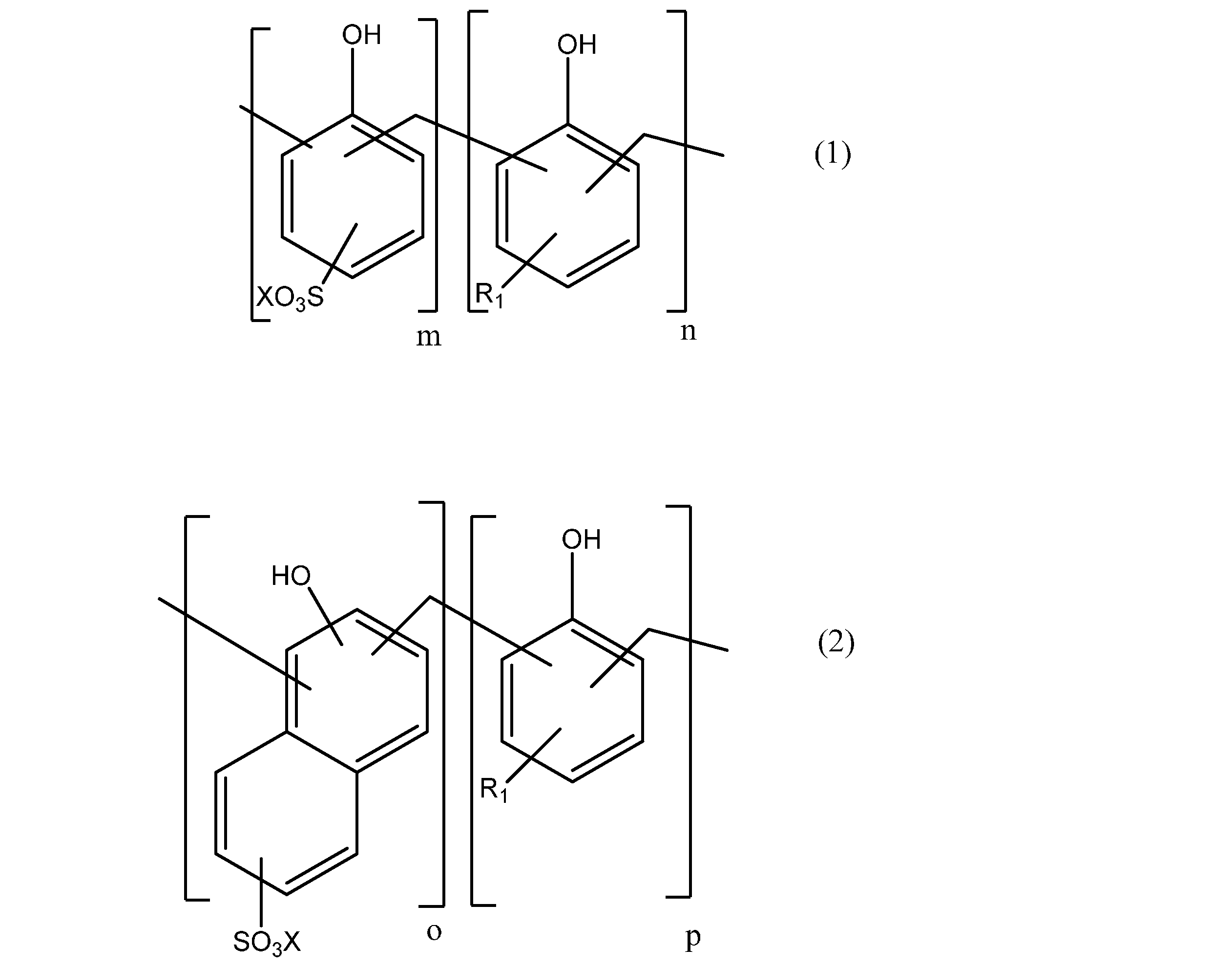
〔一般式(1)および一般式(2)中、Xは水素原子または陽イオンであり、R1は水酸基、-CH2-OH、または下記一般式(3)で表される基であり、m、n、oおよびpはそれぞれ1以上の整数である。〕

〔一般式(3)中、lは、0から4の整数であり、Qは二価の有機基であり、R2は水酸基、-CH2-OH、または水素原子である。〕
In the dispersion liquid of the present invention, the condensate (B) is preferably represented by the following general formula (1) or the following general formula (2).
[In the general formulas (1) and (2), X represents a hydrogen atom or a cation, R 1 represents a hydroxyl group, —CH 2 —OH , or a group represented by the following general formula (3), m, n, o and p are each an integer of 1 or more. ]
[In the general formula (3), l is an integer of 0 to 4, Q is a divalent organic group, and R 2 is a hydroxyl group, —CH 2 —OH, or a hydrogen atom. ]
さらに、本発明の分散液は、前記一般式(3)におけるQがスルホニル基であることが好ましい。
Further, in the dispersion liquid of the present invention, Q in the general formula (3) is preferably a sulfonyl group.
そして、本発明の分散液は、前記カーボン材料(A)が繊維状炭素ナノ構造体であることが好ましい。
In the dispersion liquid of the present invention, the carbon material (A) is preferably a fibrous carbon nanostructure.
さらに、本発明の分散液は、前記溶媒(C)が水を含み、前記分散液のpHが7未満であることが好ましい。
Further, in the dispersion liquid of the present invention, it is preferable that the solvent (C) contains water and the pH of the dispersion liquid is less than 7.
そして、本発明の分散液は、前記カーボン材料(A)100質量部当たり、前記縮合物(B)を50質量部以上500質量部以下含むことが好ましい。
The dispersion of the present invention preferably contains 50 parts by mass or more and 500 parts by mass or less of the condensate (B) per 100 parts by mass of the carbon material (A).
また、この発明は、上記課題を有利に解決することを目的とするものであり、本発明の導電膜は、上述のいずれかの分散液を用いて得られることを特徴とする。本発明の分散液を用いれば、基材との密着性に優れる導電膜を提供することができる。
Further, the present invention has an object to advantageously solve the above problems, and the conductive film of the present invention is characterized by being obtained by using any one of the above-mentioned dispersion liquids. By using the dispersion liquid of the present invention, it is possible to provide a conductive film having excellent adhesion to a substrate.
また、この発明は、上記課題を有利に解決することを目的とするものであり、本発明の電極は、上述の導電膜を備えることを特徴とする。本発明の導電膜を備える電極は、優れた導電性を有する。
Further, the present invention is intended to advantageously solve the above problems, and an electrode of the present invention is characterized by including the above-mentioned conductive film. The electrode provided with the conductive film of the present invention has excellent conductivity.
また、この発明は、上記課題を有利に解決することを目的とするものであり、本発明の太陽電池は、上述の電極を備えることを特徴とする。本発明の電極を備える太陽電池は、高い変換効率を有する。
Further, the present invention is intended to advantageously solve the above problems, and a solar cell of the present invention is characterized by including the above-mentioned electrode. The solar cell provided with the electrode of the present invention has high conversion efficiency.
また、この発明は、上記課題を有利に解決することを目的とするものであり、本発明の導電膜の製造方法は、上述のいずれかの分散液を基材上に塗布し乾燥させて導電膜を形成する工程(1)と、前記工程(1)で得られた導電膜を溶媒で洗浄し、前記導電膜から前記縮合物(B)の少なくとも一部を除去する工程(2)と、を含むことを特徴とする。本発明の導電膜の製造方法は、基材との密着性に優れる導電膜を効率よく製造することができる。
Further, the present invention is intended to advantageously solve the above problems, the method for producing a conductive film of the present invention, any one of the above dispersion is applied to the substrate and dried to conduct A step (1) of forming a film, a step (2) of washing the conductive film obtained in the step (1) with a solvent to remove at least a part of the condensate (B) from the conductive film, It is characterized by including. INDUSTRIAL APPLICABILITY The conductive film manufacturing method of the present invention can efficiently manufacture a conductive film having excellent adhesion to a substrate.
本発明によれば、基材に対する塗布性(濡れ性)を向上させることができ、基材との密着性が高い導電膜を形成することができる分散液を提供することができる。
また、本発明によれば、基材との密着性が高い導電膜およびその製造方法、該導電膜を備え、高い導電性を有する電極、並びに、該電極を備え、高い変換効率を有する太陽電池を提供することができる。 According to the present invention, it is possible to provide a dispersion liquid capable of improving the coating property (wettability) with respect to a substrate and forming a conductive film having high adhesion to the substrate.
Further, according to the present invention, a conductive film having high adhesion to a base material, a method for producing the conductive film, an electrode having the conductive film and having high conductivity, and a solar cell having the electrode and having high conversion efficiency. Can be provided.
(分散液)
本発明のカーボン材料分散液は、カーボン材料(A)、縮合物(B)、および溶媒(C)を含み、必要に応じて、任意のその他の成分をさらに含む。
本発明の分散液は、酸性であることが好ましい。分散液が酸性であることで、基板上に形成された導電層上に分散液を塗布する場合に、基板上に形成された導電層に対する浸食により、基板上に形成された導電層と分散液による導電層との密着性を向上させることができる。 (Dispersion liquid)
The carbon material dispersion liquid of the present invention contains the carbon material (A), the condensate (B), and the solvent (C), and further contains any other component as necessary.
The dispersion of the present invention is preferably acidic. When the dispersion liquid is acidic, when the dispersion liquid is applied on the conductive layer formed on the substrate, the conductive layer formed on the substrate and the dispersion liquid are eroded by the erosion of the conductive layer formed on the substrate. It is possible to improve the adhesion to the conductive layer.
<カーボン材料(A)>
カーボン材料(A)としては、特に制限されることなく、導電性を有する、繊維状炭素ナノ構造体、グラフェン、フラーレン、カーボンナノホーン、グラファイト、活性炭、カーボンファイバー、多孔質カーボン、膨張黒鉛、カーボン粒子(例えば、ケッチェンブラック、アセチレンブラック等のカーボンブラック)などを用いることができる。これらは、1種単独で使用してもよいし、2種以上を併用してもよい。
これらの中でも、得られる導電膜の強度や触媒性能に優れる点で、繊維状炭素ナノ構造体が好ましい。 <Carbon material (A)>
The carbon material (A) is not particularly limited, and has conductivity, fibrous carbon nanostructure, graphene, fullerene, carbon nanohorn, graphite, activated carbon, carbon fiber, porous carbon, expanded graphite, carbon particles. (For example, carbon black such as Ketjen black and acetylene black) can be used. These may be used alone or in combination of two or more.
Among these, the fibrous carbon nanostructure is preferable in that the conductive film obtained has excellent strength and catalytic performance.
<<繊維状炭素ナノ構造体>>
繊維状炭素ナノ構造体としては、具体的には、例えば、カップスタック型カーボンナノチューブなどの円錐状の構造体が積み重なってできた構造体、カーボンナノバット、カーボンナノチューブ(CNT)等の円筒形状の炭素ナノ構造体や、炭素の六員環ネットワークが扁平筒状に形成されてなるグラフェンナノリボン等の非円筒形状の炭素ナノ構造体などの炭素ナノ構造体を用いることができる。これらは、1種単独で使用してもよいし、2種以上を併用してもよい。 <<Fibrous carbon nanostructure>>
Specific examples of the fibrous carbon nanostructure include a structure formed by stacking conical structures such as cup-stacked carbon nanotubes, and a cylindrical shape such as carbon nanobats and carbon nanotubes (CNTs). A carbon nanostructure such as a carbon nanostructure or a non-cylindrical carbon nanostructure such as a graphene nanoribbon formed by forming a carbon six-membered ring network in a flat tubular shape can be used. These may be used alone or in combination of two or more.
そして、上述した中でも、繊維状炭素ナノ構造体としては、CNTを含む繊維状炭素ナノ構造体を用いることがより好ましい。なお、繊維状炭素ナノ構造体はCNTのみからなってもよい。CNTを含む繊維状炭素ナノ構造体を使用すれば、少ない配合量であっても、得られる導電膜に対して、導電性、膜強度、太陽電池用電極に用いる場合における触媒活性等の特性を効率的に付与することができるからである。
Further, among the above, it is more preferable to use a fibrous carbon nanostructure containing CNT as the fibrous carbon nanostructure. The fibrous carbon nanostructure may be made of CNT only. If a fibrous carbon nanostructure containing CNTs is used, even if the compounding amount is small, the obtained conductive film can have properties such as conductivity, film strength, and catalytic activity when used for a solar cell electrode. This is because it can be efficiently given.
繊維状炭素ナノ構造体中のCNTとしては、特に制限されることなく、単層カーボンナノチューブおよび/または多層カーボンナノチューブを用いることができる。CNTは、単層から5層までのカーボンナノチューブであることが好ましく、単層カーボンナノチューブであることがより好ましい。これらは、1種単独で使用してもよいし、2種以上を併用してもよい。カーボンナノチューブの層数が少ないほど、配合量が少量であっても、比表面積が大きくなり、得られる導電膜に対して、太陽電池用電極に用いる場合における触媒活性等の特性を良好に付与することができる。
CNTs in the fibrous carbon nanostructure are not particularly limited, and single-walled carbon nanotubes and/or multi-walled carbon nanotubes can be used. The CNTs are preferably single-walled to five-walled carbon nanotubes, and more preferably single-walled carbon nanotubes. These may be used alone or in combination of two or more. The smaller the number of layers of carbon nanotubes is, the larger the specific surface area is, even if the blending amount is small, so that the obtained conductive film can be provided with good properties such as catalytic activity when used as a solar cell electrode. be able to.
また、繊維状炭素ナノ構造体の平均直径は、1nm以上であることが好ましく、60nm以下であることが好ましく、30nm以下であることがより好ましく、10nm以下であることが特に好ましい。繊維状炭素ナノ構造体の平均直径が1nm以上であれば、繊維状炭素ナノ構造体の分散性を高め、導電膜に安定的に導電性等の特性を良好に付与することができる。また、繊維状炭素ナノ構造体の平均直径が60nm以下であれば、少ない配合量であっても、得られる導電膜に対して、太陽電池用電極に用いる場合における触媒活性等の特性を効率的に付与することができる。
なお、本発明において、「繊維状炭素ナノ構造体の平均直径」は、透過型電子顕微鏡(TEM)画像上で、例えば、20本の繊維状炭素ナノ構造体について直径(外径)を測定し、個数平均値を算出することで求めることができる。 The average diameter of the fibrous carbon nanostructures is preferably 1 nm or more, preferably 60 nm or less, more preferably 30 nm or less, and particularly preferably 10 nm or less. When the average diameter of the fibrous carbon nanostructures is 1 nm or more, the dispersibility of the fibrous carbon nanostructures can be enhanced and the conductive film can be stably imparted with favorable characteristics such as conductivity. In addition, if the average diameter of the fibrous carbon nanostructures is 60 nm or less, even if the compounding amount is small, the obtained conductive film can efficiently exhibit characteristics such as catalytic activity when used in a solar cell electrode. Can be given to.
In the present invention, the “average diameter of fibrous carbon nanostructures” is, for example, the diameter (outer diameter) of 20 fibrous carbon nanostructures measured on a transmission electron microscope (TEM) image. , Can be obtained by calculating the number average value.
また、繊維状炭素ナノ構造体としては、平均直径(Av)に対する、直径の標準偏差(σ:標本標準偏差)に3を乗じた値(3σ)の比(3σ/Av)が0.20超0.60未満の繊維状炭素ナノ構造体を用いることが好ましく、3σ/Avが0.25超の繊維状炭素ナノ構造体を用いることがより好ましく、3σ/Avが0.40超の繊維状炭素ナノ構造体を用いることが特に好ましい。3σ/Avが0.20超0.60未満の繊維状炭素ナノ構造体を使用すれば、製造される導電膜の性能を更に向上させることができる。
なお、繊維状炭素ナノ構造体の平均直径(Av)および標準偏差(σ)は、繊維状炭素ナノ構造体の製造方法や製造条件を変更することにより調整してもよいし、異なる製法で得られた繊維状炭素ナノ構造体を複数種類組み合わせることにより調整してもよい。 Further, as the fibrous carbon nanostructure, the ratio (3σ/Av) of the value (3σ) obtained by multiplying the standard deviation (σ: sample standard deviation) of the diameter by 3 with respect to the average diameter (Av) is more than 0.20. A fibrous carbon nanostructure of less than 0.60 is preferably used, and a fibrous carbon nanostructure of 3σ/Av of more than 0.25 is more preferably used, and a fibrous carbon of 3σ/Av of more than 0.40 is used. It is particularly preferred to use carbon nanostructures. The use of the fibrous carbon nanostructure having 3σ/Av of more than 0.20 and less than 0.60 can further improve the performance of the produced conductive film.
The average diameter (Av) and standard deviation (σ) of the fibrous carbon nanostructure may be adjusted by changing the production method or production conditions of the fibrous carbon nanostructure, or obtained by a different production method. The fibrous carbon nanostructure may be adjusted by combining a plurality of types.
そして、繊維状炭素ナノ構造体としては、前述のようにして測定した直径を横軸に、その頻度を縦軸に取ってプロットし、ガウシアンで近似した際に、正規分布を取るものが通常使用される。
And, as the fibrous carbon nanostructure, it is usually used that the diameter measured as described above is plotted on the abscissa and the frequency is plotted on the ordinate, and a normal distribution is obtained when approximated by Gaussian. To be done.
また、繊維状炭素ナノ構造体は、平均長さが、10μm以上であることが好ましく、50μm以上であることがより好ましく、80μm以上であることが特に好ましく、600μm以下であることが好ましく、500μm以下であることがより好ましく、400μm以下であることが特に好ましい。平均長さが10μm以上であれば、少ない配合量で導電膜中において導電パスを形成でき、また、導電膜の強度が高い。そして、平均長さが600μm以下であれば、分散液を塗布する際、基材への塗布性を向上させることができる。従って、繊維状炭素ナノ構造体の平均長さを上記範囲内とすれば、導電膜の表面抵抗率を十分に低下させることや導電膜に対して高い触媒活性を付与することができる。
なお、本発明において、「繊維状炭素ナノ構造体」の平均長さは、走査型電子顕微鏡(SEM)画像上で、例えば、20本の繊維状炭素ナノ構造体について長さを測定し、個数平均値を算出することで求めることができる。 The average length of the fibrous carbon nanostructure is preferably 10 μm or more, more preferably 50 μm or more, particularly preferably 80 μm or more, and preferably 600 μm or less, 500 μm It is more preferably not more than 400 μm, particularly preferably not more than 400 μm. When the average length is 10 μm or more, a conductive path can be formed in the conductive film with a small amount and the strength of the conductive film is high. When the average length is 600 μm or less, the coating property on the base material can be improved when the dispersion liquid is coated. Therefore, by setting the average length of the fibrous carbon nanostructure within the above range, it is possible to sufficiently reduce the surface resistivity of the conductive film and impart high catalytic activity to the conductive film.
In the present invention, the average length of the “fibrous carbon nanostructures” is, for example, the length of 20 fibrous carbon nanostructures measured on a scanning electron microscope (SEM) image. It can be obtained by calculating the average value.
更に、繊維状炭素ナノ構造体は、通常、アスペクト比が10超である。なお、繊維状炭素ナノ構造体のアスペクト比は、走査型電子顕微鏡または透過型電子顕微鏡を用いて、無作為に選択した繊維状炭素ナノ構造体100本の直径および長さを測定し、直径と長さとの比(長さ/直径)の平均値を算出することにより求めることができる。
Further, the fibrous carbon nanostructure usually has an aspect ratio of more than 10. In addition, the aspect ratio of the fibrous carbon nanostructures was determined by measuring the diameter and length of 100 randomly selected fibrous carbon nanostructures using a scanning electron microscope or a transmission electron microscope. It can be determined by calculating the average value of the ratio to the length (length/diameter).
また、繊維状炭素ナノ構造体は、BET比表面積が、200m2/g以上であることが好ましく、400m2/g以上であることがより好ましく、600m2/g以上であることが特に好ましく、2000m2/g以下であることが好ましく、1800m2/g以下であることがより好ましく、1600m2/g以下であることが特に好ましい。繊維状炭素ナノ構造体のBET比表面積が200m2/g以上であれば、繊維状炭素ナノ構造体の分散性を高め、少ない配合量で、得られる導電膜に対して、導電性、太陽電池用電極に用いる場合における触媒活性等の特性を良好に付与することができる。また、繊維状炭素ナノ構造体のBET比表面積が2000m2/g以下であれば、得られる導電膜に対して、導電性、太陽電池用電極に用いる場合における触媒活性等の特性を良好に付与することができ、また、分散液の塗布性を安定化させることができる。
なお、本発明において、「BET比表面積」とは、BET法を用いて測定した窒素吸着比表面積を指す。 Further, the fibrous carbon nanostructure has a BET specific surface area of preferably 200 m 2 /g or more, more preferably 400 m 2 /g or more, particularly preferably 600 m 2 /g or more, It is preferably 2000 m 2 /g or less, more preferably 1800 m 2 /g or less, and particularly preferably 1600 m 2 /g or less. When the BET specific surface area of the fibrous carbon nanostructures is 200 m 2 /g or more, the dispersibility of the fibrous carbon nanostructures is increased, and the conductive film and the solar cell with respect to the conductive film obtained can be obtained with a small amount. It is possible to satisfactorily impart characteristics such as catalytic activity when used as a working electrode. In addition, when the BET specific surface area of the fibrous carbon nanostructure is 2000 m 2 /g or less, the obtained conductive film is satisfactorily imparted with properties such as conductivity and catalytic activity when used as a solar cell electrode. The coating property of the dispersion liquid can be stabilized.
In addition, in this invention, "BET specific surface area" refers to the nitrogen adsorption specific surface area measured using the BET method.
また、繊維状炭素ナノ構造体は、吸着等温線から得られるt-プロットが上に凸な形状を示すことが好ましい。なお、「t-プロット」は、窒素ガス吸着法により測定された繊維状炭素ナノ構造体の吸着等温線において、相対圧を窒素ガス吸着層の平均厚みt(nm)に変換することにより得ることができる。すなわち、窒素ガス吸着層の平均厚みtを相対圧P/P0に対してプロットした、既知の標準等温線から、相対圧に対応する窒素ガス吸着層の平均厚みtを求めて上記変換を行うことにより、繊維状炭素ナノ構造体のt-プロットが得られる(de Boerらによるt-プロット法)。
Also, the fibrous carbon nanostructure preferably has a t-plot obtained from the adsorption isotherm showing a convex shape. The “t-plot” is obtained by converting the relative pressure into the average thickness t (nm) of the nitrogen gas adsorption layer in the adsorption isotherm of the fibrous carbon nanostructure measured by the nitrogen gas adsorption method. You can That is, from the known standard isotherm obtained by plotting the average thickness t of the nitrogen gas adsorption layer against the relative pressure P/P0, obtain the average thickness t of the nitrogen gas adsorption layer corresponding to the relative pressure and perform the above conversion. Gives a t-plot of the fibrous carbon nanostructure (t-plot method by de Boer et al.).
ここで、表面に細孔を有する物質では、窒素ガス吸着層の成長は、次の(1)~(3)の過程に分類される。そして、下記の(1)~(3)の過程によって、t-プロットの傾きに変化が生じる。
(1)全表面への窒素分子の単分子吸着層形成過程
(2)多分子吸着層形成とそれに伴う細孔内での毛管凝縮充填過程
(3)細孔が窒素によって満たされた見かけ上の非多孔性表面への多分子吸着層形成過程 Here, in a substance having pores on the surface, the growth of the nitrogen gas adsorption layer is classified into the following processes (1) to (3). Then, the slopes of the t-plot change due to the following processes (1) to (3).
(1) Monomolecular adsorption layer formation process of nitrogen molecules on the whole surface (2) Multimolecular adsorption layer formation and accompanying capillary condensation filling process in pores (3) Apparently pores filled with nitrogen Formation process of multi-molecular adsorption layer on non-porous surface
そして、上に凸な形状を示すt-プロットは、窒素ガス吸着層の平均厚みtが小さい領域では、原点を通る直線上にプロットが位置するのに対し、tが大きくなると、プロットが当該直線から下にずれた位置となる。かかるt-プロットの形状を有する繊維状炭素ナノ構造体は、繊維状炭素ナノ構造体の全比表面積に対する内部比表面積の割合が大きく、繊維状炭素ナノ構造体を構成する炭素ナノ構造体に多数の開口が形成されていることを示している。
The t-plot showing the upward convex shape is located on a straight line passing through the origin in the region where the average thickness t of the nitrogen gas adsorption layer is small, whereas when t becomes large, the plot becomes the straight line. The position is shifted downward from. The fibrous carbon nanostructure having the shape of the t-plot has a large ratio of the internal specific surface area to the total specific surface area of the fibrous carbon nanostructure, and many carbon nanostructures constituting the fibrous carbon nanostructure. Indicates that an opening is formed.
なお、繊維状炭素ナノ構造体のt-プロットの屈曲点は、0.2≦t(nm)≦1.5を満たす範囲にあることが好ましく、0.45≦t(nm)≦1.5の範囲にあることがより好ましく、0.55≦t(nm)≦1.0の範囲にあることが特に好ましい。繊維状炭素ナノ構造体のt-プロットの屈曲点がかかる範囲内にあれば、繊維状炭素ナノ構造体の分散性を高め、少ない配合量で導電膜の導電性等の特性を高めることができる。具体的には、屈曲点の値が0.2未満であれば、繊維状炭素ナノ構造体が凝集し易く分散性が低下し、屈曲点の値が1.5超であれば繊維状炭素ナノ構造体同士が絡み合いやすくなり分散性が低下する虞がある。
なお、「屈曲点の位置」は、前述した(1)の過程の近似直線Aと、前述した(3)の過程の近似直線Bとの交点である。 The bending point of the t-plot of the fibrous carbon nanostructure is preferably in the range of 0.2≦t(nm)≦1.5, and 0.45≦t(nm)≦1.5. Is more preferable, and 0.55≦t(nm)≦1.0 is particularly preferable. When the inflection point of the t-plot of the fibrous carbon nanostructure is within such a range, the dispersibility of the fibrous carbon nanostructure can be enhanced, and the properties such as conductivity of the conductive film can be enhanced with a small amount of compounding. .. Specifically, if the value of the bending point is less than 0.2, the fibrous carbon nanostructures are likely to aggregate and the dispersibility decreases, and if the value of the bending point exceeds 1.5, the fibrous carbon nanostructure is formed. The structures may be easily entangled with each other and the dispersibility may be reduced.
The "position of the bending point" is the intersection of the approximate straight line A in the above process (1) and the approximate straight line B in the above process (3).
更に、繊維状炭素ナノ構造体は、t-プロットから得られる全比表面積S1に対する内部比表面積S2の比(S2/S1)が0.05以上0.30以下であるのが好ましい。繊維状炭素ナノ構造体のS2/S1の値がかかる範囲内であれば、繊維状炭素ナノ構造体の分散性を高め、少ない配合量で導電膜の導電性等の特性を高めることができる。
ここで、繊維状炭素ナノ構造体の全比表面積S1および内部比表面積S2は、そのt-プロットから求めることができる。具体的には、まず、(1)の過程の近似直線の傾きから全比表面積S1を、(3)の過程の近似直線の傾きから外部比表面積S3を、それぞれ求めることができる。そして、全比表面積S1から外部比表面積S3を差し引くことにより、内部比表面積S2を算出することができる。 Further, in the fibrous carbon nanostructure, the ratio (S2/S1) of the internal specific surface area S2 to the total specific surface area S1 obtained from the t-plot is preferably 0.05 or more and 0.30 or less. When the value of S2/S1 of the fibrous carbon nanostructure is within such a range, the dispersibility of the fibrous carbon nanostructure can be enhanced and the properties such as the conductivity of the conductive film can be enhanced with a small blending amount.
Here, the total specific surface area S1 and the internal specific surface area S2 of the fibrous carbon nanostructure can be obtained from its t-plot. Specifically, first, the total specific surface area S1 can be obtained from the slope of the approximate straight line in the process (1), and the external specific surface area S3 can be obtained from the slope of the approximate straight line in the process (3). Then, the internal specific surface area S2 can be calculated by subtracting the external specific surface area S3 from the total specific surface area S1.
因みに、繊維状炭素ナノ構造体の吸着等温線の測定、t-プロットの作成、および、t-プロットの解析に基づく全比表面積S1と内部比表面積S2との算出は、例えば、市販の測定装置である「BELSORP(登録商標)-mini」(日本ベル(株)製)を用いて行うことができる。
Incidentally, the measurement of the adsorption isotherm of the fibrous carbon nanostructure, the preparation of the t-plot, and the calculation of the total specific surface area S1 and the internal specific surface area S2 based on the analysis of the t-plot are carried out by using, for example, a commercially available measuring device. "BELSORP (registered trademark)-mini" (manufactured by Nippon Bell Co., Ltd.) can be used.
更に、繊維状炭素ナノ構造体として好適なCNTを含む繊維状炭素ナノ構造体は、ラマン分光法を用いて評価した際に、Radial Breathing Mode(RBM)のピークを有することが好ましい。なお、三層以上の多層カーボンナノチューブのみからなる繊維状炭素ナノ構造体のラマンスペクトルには、RBMが存在しない。
Furthermore, it is preferable that the fibrous carbon nanostructure containing CNT suitable as the fibrous carbon nanostructure has a peak of Radial Breathing Mode (RBM) when evaluated using Raman spectroscopy. It should be noted that RBM does not exist in the Raman spectrum of the fibrous carbon nanostructure composed of only multi-walled carbon nanotubes having three or more layers.
また、CNTを含む繊維状炭素ナノ構造体は、ラマンスペクトルにおけるDバンドピーク強度に対するGバンドピーク強度の比(G/D比)が、0.5以上10.0以下であることが好ましく、1.0以上5.0以下であることがより好ましい。G/D比が0.5以上10.0以下であれば、得られる導電膜に対して、太陽電池用電極に用いる場合における触媒活性等の特性を良好に付与することができる。
Further, in the fibrous carbon nanostructure containing CNT, the ratio of the G band peak intensity to the D band peak intensity (G/D ratio) in the Raman spectrum is preferably 0.5 or more and 10.0 or less, and 1 It is more preferably from 0.0 to 5.0. When the G/D ratio is 0.5 or more and 10.0 or less, characteristics such as catalytic activity when used for a solar cell electrode can be favorably imparted to the obtained conductive film.
また、CNTを含む繊維状炭素ナノ構造体は、XPSによる元素分析で、炭素原子と酸素原子の合計に対し、酸素原子量が5原子%以下であることが好ましく、2原子%以下であることがより好ましく、1原子%以下であることが特に好ましい。酸素原子量が好ましい範囲内であれば、得られる導電膜に対して、太陽電池用電極に用いる場合における触媒活性等の特性を良好に付与することができる。
The fibrous carbon nanostructure containing CNTs preferably has an oxygen atom amount of 5 atom% or less, and preferably 2 atom% or less, based on the total of carbon atoms and oxygen atoms by XPS elemental analysis. More preferably, it is particularly preferably 1 atomic% or less. When the amount of oxygen atoms is within the preferable range, it is possible to favorably provide the obtained conductive film with properties such as catalytic activity when used in a solar cell electrode.
CNTを含む繊維状炭素ナノ構造体は、CHNの元素分析による、炭素原子の割合は、85質量%以上であることが好ましく、90質量%以上であることがより好ましく、95質量%以上であることがさらに好ましく、98質量%以上であることが特に好ましく、水素原子の割合は、1質量%以下であることが好ましく、0.8質量%以下であることがより好ましく、0.3質量%以下であることがより好ましく、0.1質量%以下であることが特に好ましい。
炭素原子(水素原子)の割合が好ましい範囲内であれば、得られる導電膜に対して、太陽電池用電極に用いる場合における触媒活性等の特性を良好に付与することができる。 In the fibrous carbon nanostructure containing CNT, the proportion of carbon atoms is preferably 85% by mass or more, more preferably 90% by mass or more, and 95% by mass or more by elemental analysis of CHN. More preferably, it is particularly preferably 98 mass% or more, the proportion of hydrogen atoms is preferably 1 mass% or less, more preferably 0.8 mass% or less, 0.3 mass% The content is more preferably the following or less, and particularly preferably 0.1% by mass or less.
When the ratio of carbon atoms (hydrogen atoms) is within the preferable range, it is possible to satisfactorily provide the obtained conductive film with properties such as catalytic activity when used for a solar cell electrode.
なお、CNTを含む繊維状炭素ナノ構造体は、特に制限されることなく、アーク放電法、レーザーアブレーション法、化学的気相成長法(CVD法)などの既知のCNTの合成方法を用いて製造することができる。具体的には、CNTを含む繊維状炭素ナノ構造体は、例えば、カーボンナノチューブ製造用の触媒層を表面に有する基材上に原料化合物およびキャリアガスを供給し、化学的気相成長法(CVD法)によりCNTを合成する際に、系内に微量の酸化剤(触媒賦活物質)を存在させることで、触媒層の触媒活性を飛躍的に向上させるという方法(スーパーグロース法;国際公開第2006/011655号参照)に準じて、効率的に製造することができる。なお、以下では、スーパーグロース法により得られるカーボンナノチューブを「SGCNT」と称することがある。
そして、スーパーグロース法により製造された繊維状炭素ナノ構造体は、SGCNTのみから構成されていてもよいし、SGCNTに加え、例えば、非円筒形状の炭素ナノ構造体等の他の炭素ナノ構造体を含んでいてもよい。 The fibrous carbon nanostructure containing CNTs is not particularly limited, and is manufactured using a known CNT synthesis method such as an arc discharge method, a laser ablation method, or a chemical vapor deposition method (CVD method). can do. Specifically, a fibrous carbon nanostructure containing CNTs is prepared by, for example, supplying a raw material compound and a carrier gas onto a base material having a catalyst layer for producing carbon nanotubes on the surface thereof and performing chemical vapor deposition (CVD). Method), by which a small amount of an oxidizing agent (catalyst activating substance) is present in the system when CNTs are synthesized by the method (super growth method; WO 2006). /011655), and can be efficiently produced. Note that, hereinafter, the carbon nanotube obtained by the super growth method may be referred to as “SGCNT”.
The fibrous carbon nanostructure manufactured by the super growth method may be composed of only SGCNT, or in addition to SGCNT, for example, another carbon nanostructure such as a non-cylindrical carbon nanostructure. May be included.
分散液中のカーボン材料(A)の含有量は、特に制限されないが、分散液全体中、0.001質量%以上であることが好ましく、0.01質量%以上であることがより好ましく、0.1質量%以上であることが特に好ましく、30.0質量%以下であることが好ましく、10.0質量%以下であることがより好ましく、5.0質量%以下であることがさらに好ましく、1.0質量%以下であることが特に好ましい。
The content of the carbon material (A) in the dispersion is not particularly limited, but is preferably 0.001 mass% or more, more preferably 0.01 mass% or more, and 0 in the entire dispersion. 0.1 mass% or more is particularly preferable, 30.0 mass% or less is preferable, 10.0 mass% or less is more preferable, 5.0 mass% or less is further preferable, It is particularly preferably 1.0% by mass or less.
<縮合物(B)>
縮合物(B)は、芳香族スルホン酸化合物とヒドロキシフェノール化合物とアルデヒド化合物との縮合物であり、カーボン材料(A)の分散剤として機能する。
縮合物(B)はCNT等のカーボン材料(A)の分散性に優れ、また、溶媒洗浄により除去容易であるため、触媒活性が向上し、密着性が高く、また膜自体の強度の高い導電膜が得られ、ひいては、良好な対向電極等の電極を得ることができる。 <Condensate (B)>
The condensate (B) is a condensate of an aromatic sulfonic acid compound, a hydroxyphenol compound and an aldehyde compound, and functions as a dispersant for the carbon material (A).
Since the condensate (B) has excellent dispersibility of the carbon material (A) such as CNT and is easily removed by washing with a solvent, the catalytic activity is improved, the adhesion is high, and the strength of the film itself is high. A film can be obtained, and thus an excellent electrode such as a counter electrode can be obtained.
<<芳香族スルホン酸化合物>>
「芳香族スルホン酸化合物」は、「芳香族化合物における水素原子の何れかが-SO3X(Xは水素原子または陽イオン)で置換された化合物」を意味する。
芳香族スルホン酸化合物としては、例えば、p-フェノールスルホン酸、o-フェノールスルホン酸、フェノールジスルホン酸等のフェノールスルホン酸(PSA);1-ナフトール-4―スルホン酸、2-ナフトール-6-スルホン酸、2-ナフトール-7-スルホン酸、1-ナフトール-6-スルホン酸、2-ナフトール-8-スルホン酸等のナフトールスルホン酸;4-アミノナフタレンスルホン酸等のナフタレンスルホン酸;スルファニル酸(4-アミノベンゼンスルホン酸);などが挙げられる。これらは、1種類を単独で用いてもよく、2種類以上を任意の比率で組み合わせて用いてもよい。
これらの中でも、縮合反応性、および、生成した縮合物の溶媒への溶解性の点で、フェノールスルホン酸(PSA)、4-アミノベンゼンスルホン酸が好ましい。 << aromatic sulfonic acid compound >>
“Aromatic sulfonic acid compound” means “a compound in which any of hydrogen atoms in an aromatic compound is replaced by —SO 3 X (X is a hydrogen atom or a cation)”.
Examples of the aromatic sulfonic acid compound include phenolsulfonic acid (PSA) such as p-phenolsulfonic acid, o-phenolsulfonic acid and phenoldisulfonic acid; 1-naphthol-4-sulfonic acid, 2-naphthol-6-sulfone. Acid, 2-naphthol-7-sulfonic acid, 1-naphthol-6-sulfonic acid, 2-naphthol-8-sulfonic acid and other naphtholsulfonic acids; 4-aminonaphthalenesulfonic acid and other naphthalenesulfonic acids; sulfanilic acid (4 -Aminobenzenesulfonic acid); and the like. These may be used individually by 1 type and may be used in combination of 2 or more types by arbitrary ratios.
Among these, phenol sulfonic acid (PSA) and 4-aminobenzene sulfonic acid are preferable in terms of condensation reactivity and solubility of the generated condensate in a solvent.
<<ヒドロキシフェノール化合物>>
「ヒドロキシフェノール化合物」は、「ヒドロキシ基(水酸基)を1個以上有する化合物」であって「芳香族スルホン酸化合物」以外のものを意味する。
ヒドロキシフェノール化合物は、例えば、ビスフェノールA、4,4-ビフェノール、3,3,5,5-テトラメチル-4,4-ビフェノール、ビス(4-ヒドロキシ-3,5-ジメチルフェニル)メタン等のヒドロキシフェノール;2,7-ジヒドロキシナフタレン、1,6-ジヒドロキシナフタレン、1,1-ビス(2-ナフトール)等のナフタレン骨格を有するもの;4,4’-ジヒドロキシジフェニルスルホン、2,4’-ジヒドロキシジフェニルスルホン、ビス(4-ヒドロキシ-3,5-ジメチルフェニル)スルホン等のヒドロキシジフェニルスルホン(BS);1,1,1-トリス(4-ヒドロキシフェニル)メタン、1,1,2,2、-テトラキス(4-ヒドロキシフェニル)エタン等の多官能フェノール類;などが挙げられる。これらは、1種類を単独で用いてもよく、2種類以上を任意の比率で組み合わせて用いてもよい。
これらの中でも、製造の容易さ、基材との接着性、生成した縮合物の溶媒への溶解性の点で、ジヒドロキシジフェニルスルホン等の水酸基を2個以上4個以下有し、六員環を1個以上3個以下有し、スルホニル基等の連結基を有する化合物、が好ましい。 << hydroxyphenol compound >>
"Hydroxyphenol compound" means "a compound having at least one hydroxy group (hydroxyl group)" and other than "aromatic sulfonic acid compound".
Examples of the hydroxyphenol compound include hydroxy such as bisphenol A, 4,4-biphenol, 3,3,5,5-tetramethyl-4,4-biphenol, and bis(4-hydroxy-3,5-dimethylphenyl)methane. Phenol; those having a naphthalene skeleton such as 2,7-dihydroxynaphthalene, 1,6-dihydroxynaphthalene, 1,1-bis(2-naphthol); 4,4'-dihydroxydiphenyl sulfone, 2,4'-dihydroxydiphenyl Hydroxydiphenylsulfone (BS) such as sulfone and bis(4-hydroxy-3,5-dimethylphenyl)sulfone; 1,1,1-tris(4-hydroxyphenyl)methane, 1,1,2,2,-tetrakis And polyfunctional phenols such as (4-hydroxyphenyl)ethane; and the like. These may be used individually by 1 type and may be used in combination of 2 or more types by arbitrary ratios.
Among these, from the viewpoint of ease of production, adhesion to a base material, and solubility of the resulting condensate in a solvent, it has 2 to 4 hydroxyl groups such as dihydroxydiphenyl sulfone and has a 6-membered ring. A compound having 1 or more and 3 or less and a linking group such as a sulfonyl group is preferable.
<<アルデヒド化合物>>
アルデヒド化合物としては、ホルムアルデヒド、アセトアルデヒド、プロピオンアルデヒド、n-ブチルアルデヒド、イソブチルアルデヒド、グリオキサール等の脂肪族アルデヒド;フルフラール、ベンゾアルデヒド、サリチルアルデヒド、パラホルムアルデヒド等の環状構造をもつアルデヒド;等が挙げられる。
アルデヒド化合物としては、水溶液を用いてもよい。
アルデヒド化合物は、芳香族スルホン酸化合物と、ヒドロキシフェノール化合物との総使用量に対して、0.5倍モル以上2倍モル以下程度使用するのが好ましく、1.0倍モル以上1.9倍モル以下程度使用するのがより好ましい。上記下限以上であると、反応終了時の未反応の芳香族スルホン酸化合物およびヒドロキシフェノール化合物が多く残存するのを抑制することができ、上記上限以下であると、縮合物液中の遊離アルデヒド化合物が多くなるのを抑制することができる。 << aldehyde compound >>
Examples of the aldehyde compound include aliphatic aldehydes such as formaldehyde, acetaldehyde, propionaldehyde, n-butyraldehyde, isobutyraldehyde, and glyoxal; aldehydes having a cyclic structure such as furfural, benzaldehyde, salicylaldehyde, and paraformaldehyde;
An aqueous solution may be used as the aldehyde compound.
The aldehyde compound is preferably used in an amount of 0.5 times or more and 2 times or less, and 1.0 times or more and 1.9 times the total amount of the aromatic sulfonic acid compound and the hydroxyphenol compound used. It is more preferable to use about a molar amount or less. When it is at least the above lower limit, a large amount of unreacted aromatic sulfonic acid compound and hydroxyphenol compound at the end of the reaction can be suppressed, and when it is at most the above upper limit, the free aldehyde compound in the condensate liquid Can be suppressed.
芳香族スルホン酸化合物とヒドロキシフェノール化合物とアルデヒド化合物との縮合反応は、公知の方法により行われる。
例えば、芳香族スルホン酸化合物とヒドロキシフェノール化合物とアルデヒド化合物とを、酸触媒またはアルカリ触媒下で、縮合反応させてアルデヒド縮合物(縮合物(B))を製造する。
芳香族スルホン酸化合物とヒドロキシフェノール化合物とアルデヒド化合物とを縮合反応させるに際し、溶媒としては、水、アルコール等が使用される。 The condensation reaction of the aromatic sulfonic acid compound, the hydroxyphenol compound and the aldehyde compound is performed by a known method.
For example, an aromatic sulfonic acid compound, a hydroxyphenol compound and an aldehyde compound are subjected to a condensation reaction under an acid catalyst or an alkali catalyst to produce an aldehyde condensate (condensate (B)).
When the condensation reaction of the aromatic sulfonic acid compound, the hydroxyphenol compound and the aldehyde compound is performed, water, alcohol or the like is used as a solvent.
酸触媒としては、例えば、塩酸、硫酸、蓚酸、酢酸、トルエンスルホン酸、などが挙げられる。これらは、1種類を単独で用いてもよく、2種類以上を任意の比率で組み合わせて用いてもよい。
アルカリ触媒としては、例えば、水酸化ナトリウム、水酸化カリウム等のアルカリ金属水酸化物;水酸化カルシウム、水酸化バリウム等のアルカリ土類金属水酸化物;アンモニア、トリエチルアミン等のアミン類;などが挙げられる。これらは、1種類を単独で用いてもよく、2種類以上を任意の比率で組み合わせて用いてもよい。これらの中でも、操作の簡便性の点で、水酸化ナトリウムが好ましい。
後述する縮合物(B)の構造として、ノボラック型を作製する場合は酸触媒、レゾール型を作製する場合は、アルカリ触媒を選択するとよい。
ところで、アルカリ触媒存在下で、芳香族スルホン酸化合物とヒドロキシフェノール化合物とアルデヒド化合物とを縮合反応させるに際しては、反応系に存在する強酸性成分を中和するのに必要なアルカリ量が使用される。ここで、反応系に存在する強酸性成分としては、遊離の硫酸並びにフェノール類に結合しているスルホン酸基が挙げられる。 Examples of the acid catalyst include hydrochloric acid, sulfuric acid, oxalic acid, acetic acid, toluenesulfonic acid, and the like. These may be used individually by 1 type and may be used in combination of 2 or more types by arbitrary ratios.
Examples of the alkali catalyst include alkali metal hydroxides such as sodium hydroxide and potassium hydroxide; alkaline earth metal hydroxides such as calcium hydroxide and barium hydroxide; amines such as ammonia and triethylamine; To be These may be used individually by 1 type and may be used in combination of 2 or more types by arbitrary ratios. Among these, sodium hydroxide is preferable from the viewpoint of easy operation.
As the structure of the condensate (B) described later, an acid catalyst may be selected when a novolac type is prepared, and an alkali catalyst is selected when a resol type is prepared.
By the way, in the condensation reaction of an aromatic sulfonic acid compound, a hydroxyphenol compound and an aldehyde compound in the presence of an alkali catalyst, the amount of alkali necessary to neutralize the strongly acidic component present in the reaction system is used. .. Here, examples of the strongly acidic component present in the reaction system include free sulfuric acid and sulfonic acid groups bonded to phenols.
縮合物(B)を調製するに際し、反応温度、反応時間は特に制限はなく、所望の重量平均分子量(標準ポリエチレングリコール換算)の縮合物(B)の製造が管理上容易となる反応温度、反応時間を適宜選択すればよい。
When the condensate (B) is prepared, the reaction temperature and the reaction time are not particularly limited, and the reaction temperature and the reaction that facilitate the production of the condensate (B) having a desired weight average molecular weight (standard polyethylene glycol conversion) from the viewpoint of management. The time may be selected appropriately.
反応温度としては、特に制限されないが、60℃以上であることが好ましく、120℃以下であることが好ましい。
反応時間としては、特に制限されないが、3時間以上であることが好ましく、20時間以下であることが好ましい。
得られたホルムアルデヒド縮合物は、縮合反応後に単離してもよいし、反応生成物をそのまま使用してもよい。 The reaction temperature is not particularly limited, but it is preferably 60° C. or higher, and preferably 120° C. or lower.
The reaction time is not particularly limited, but is preferably 3 hours or longer, and preferably 20 hours or shorter.
The obtained formaldehyde condensate may be isolated after the condensation reaction, or the reaction product may be used as it is.
縮合物(B)の構造は、例えばランダムノボラック、ハイオルトノボラックなどノボラック型(熱可塑型)、ベンジルエーテルレゾール、アンモニアレゾール、アルカリレゾールなどレゾール型(熱硬化型)などがある。分散液を塗布乾燥した後の、CNT等のカーボン材料(A)と基材との密着性の観点から、縮合物(B)の構造は、レゾール型であることが好ましく、下記一般式(1)または下記一般式(2)で表されることがより好ましい。
〔一般式(1)および一般式(2)中、Xは水素原子または陽イオンであり、R1は水酸基、-CH2-OH、または下記一般式(3)で表される基であり、m、n、o、およびpは、それぞれ、1以上の整数であり、好ましくは、1≦m≦235の整数、1≦n≦206の整数、1≦o≦192の整数、1≦p≦206の整数である。〕

〔一般式(3)中、lは0から4の整数であり、Qは、二価の有機基(例えば、-CH2-、―C(CH3)2-、-S-、-SO2-(スルホニル基)、-NH-、-N=N-)、好ましくは、-S-、-SO2-(スルホニル基)であり、より好ましくは-SO2-(スルホニル基)であり、R2は水酸基、-CH2-OH、または水素原子である。〕
The structure of the condensate (B) includes, for example, novolak type (thermoplastic type) such as random novolac and high ortho novolac, and resol type (thermosetting type) such as benzyl ether resole, ammonia resole, and alkali resole. From the viewpoint of the adhesion between the carbon material (A) such as CNT and the substrate after the dispersion is applied and dried, the condensate (B) preferably has a structure of the resol type, and has the following general formula (1) Or more preferably represented by the following general formula (2).
[In the general formulas (1) and (2), X is a hydrogen atom or a cation, R 1 is a hydroxyl group, —CH 2 —OH, or a group represented by the following general formula (3), m, n, o, and p are each an integer of 1 or more, preferably an integer of 1≦m≦235, an integer of 1≦n≦206, an integer of 1≦o≦192, and 1≦p≦ It is an integer of 206. ]
[In the general formula (3), l is an integer of 0 to 4, and Q is a divalent organic group (eg, —CH 2 —, —C(CH 3 ) 2 —, —S—, —SO 2 - (sulfonyl group), - NH -, - N = N-), preferably, -S -, - SO 2 - a (sulfonyl group), more preferably -SO 2 - a (sulfonyl group), R 2 is a hydroxyl group, —CH 2 —OH, or a hydrogen atom. ]
なお、一般式(1)におけるXとしての陽イオンは、例えば、リチウムイオン、ナトリウムイオン、カリウムイオン、カルシウムイオン、マグネシウムイオン、アンモニウムイオンなどが挙げられる。
The cation as X in the general formula (1) includes, for example, lithium ion, sodium ion, potassium ion, calcium ion, magnesium ion, ammonium ion and the like.
縮合物(B)中における、芳香族スルホン酸化合物に由来する芳香族スルホン酸化合物単量体単位に対するヒドロキシフェノール化合物に由来するヒドロキシフェノール化合物単量体単位のモル比(ヒドロキシフェノール化合物単量体単位/芳香族スルホン酸化合物単量体単位)は、1/9以上であることが好ましく、1/5以上であることがより好ましく、1/4以上であることがさらに好ましく、1/3以上であることが特に好ましく、9/1以下であることが好ましく、5/1以下であることがより好ましく、4/1以下であることがさらに好ましく、3/1以下であることが特に好ましい。
上記モル比が、上記下限以上であることにより、縮合物(B)の溶媒(C)への溶解性を向上させて、基材への密着性が高い導電膜を形成することができ、上記上限以下であることにより、カーボン材料(A)の分散性を向上させることができる。 In the condensate (B), the molar ratio of the hydroxyphenol compound monomer unit derived from the hydroxyphenol compound to the aromatic sulfonic acid compound monomer unit derived from the aromatic sulfonic acid compound (hydroxyphenol compound monomer unit /Aromatic sulfonic acid compound monomer unit) is preferably 1/9 or more, more preferably 1/5 or more, further preferably 1/4 or more, and 1/3 or more. It is particularly preferable that it is 9/1 or less, more preferably 5/1 or less, still more preferably 4/1 or less, and particularly preferably 3/1 or less.
When the above molar ratio is at least the above lower limit, the solubility of the condensate (B) in the solvent (C) can be improved, and a conductive film having high adhesion to the substrate can be formed. When it is at most the upper limit, the dispersibility of the carbon material (A) can be improved.
縮合物(B)の重量平均分子量(標準ポリエチレングリコール換算)は、500以上であることが好ましく、1,000以上であることがより好ましく、2,000以上であることがさらに好ましく、5,000以上であることが特に好ましく、100,000以下であることが好ましく、50,000以下であることがより好ましく、30,000以下であることが特に好ましい。
縮合物(B)の重量平均分子量(標準ポリエチレングリコール換算)が、上記下限以上であることにより、得られる導電膜に対して、基材との密着性および膜強度を十分付与することができ、上記上限以下であることにより、カーボン材料の分散性、得られる導電膜のリンス性、得られる電極の電極性能が優れる。 The weight average molecular weight (calculated as standard polyethylene glycol) of the condensate (B) is preferably 500 or more, more preferably 1,000 or more, further preferably 2,000 or more, and 5,000. It is particularly preferable that it is not less than 100, preferably 100,000 or less, more preferably 50,000 or less, and particularly preferably 30,000 or less.
When the weight-average molecular weight (converted to standard polyethylene glycol) of the condensate (B) is at least the above lower limit, sufficient adhesion to the substrate and film strength can be imparted to the obtained conductive film. When it is at most the above upper limit, the dispersibility of the carbon material, the rinsing property of the obtained conductive film, and the electrode performance of the obtained electrode will be excellent.
カーボン材料(A)100質量部当たりの縮合物(B)の含有量は、50質量部以上であることが好ましく、80質量部以上であることがより好ましく、130質量部以上であることが特に好ましく、500質量部以下であることが好ましく、350質量部以下であることがより好ましく、250質量部以下であることが特に好ましい。
上記含有量が、上記下限以上であることにより、得られる導電膜に対して、基材との密着性および膜強度を十分付与することができ、上記上限以下であることにより、カーボン材料の分散性、リンス性、得られる電極の電極性能が優れる。 The content of the condensate (B) per 100 parts by mass of the carbon material (A) is preferably 50 parts by mass or more, more preferably 80 parts by mass or more, and particularly preferably 130 parts by mass or more. It is preferably 500 parts by mass or less, more preferably 350 parts by mass or less, and particularly preferably 250 parts by mass or less.
When the content is at least the above lower limit, it is possible to sufficiently impart the adhesiveness to the substrate and the film strength to the obtained conductive film, and when it is at most the above upper limit, the dispersion of the carbon material is achieved. , Excellent rinsing properties and electrode performance of the obtained electrode.
<溶媒(C)>
溶媒(C)は、水系でも有機溶剤系でもよいが、水系溶媒を用いることが好ましい(すなわち、溶媒(C)が水を含むことが好ましい)。ここで水系溶媒としては、その中でCNT等のカーボン材料(A)が分散しうるものであれば特に制限されず、水を単独で使用してもよく、水と混和する溶媒類の混合溶媒を用いてもよい。水と混和する溶媒としては、エーテル類(ジオキサン、テトラヒドロフラン、メチルセロソルブ、エチレングリコールジメチルエーテル、エチレングリコールブチルエーテル等)、エーテルアルコール(エトキシエタノール、メトキシエトキシエタノール等)、エステル類(酢酸メチル、酢酸エチル等)、ケトン類(アセトン、メチルイソブチルケトン、シクロヘキサノン、メチルエチルケトン等)、アルコール類(メタノール、エタノール、イソプロパノール、プロピレングリコール、エチレングリコール、ジアセトンアルコール、フェノール等)、低級カルボン酸(酢酸等)、アミン類(トリエチルアミン、トリメタノールアミン等)、窒素含有極性溶媒(N,N-ジメチルホルムアミド、ニトロメタン、N-メチルピロリドン、アセトニトリル等)、硫黄化合物類(ジメチルスルホキシド等)などを挙げることができる。これらは、1種類を単独で用いてもよく、2種類以上を任意の比率で組み合わせて用いてもよい。
これらの中でも、水と混和する溶媒としては、分散液の安定性を向上させる観点からは、エーテル類、ケトン類、アルコール類が好ましい。
これらは、脱気などを適時行ってもよい。 <Solvent (C)>
The solvent (C) may be an aqueous solvent or an organic solvent solvent, but it is preferable to use an aqueous solvent (that is, the solvent (C) preferably contains water). Here, the aqueous solvent is not particularly limited as long as the carbon material (A) such as CNT can be dispersed therein, and water may be used alone, or a mixed solvent of solvents miscible with water. May be used. As a solvent miscible with water, ethers (dioxane, tetrahydrofuran, methyl cellosolve, ethylene glycol dimethyl ether, ethylene glycol butyl ether, etc.), ether alcohols (ethoxyethanol, methoxyethoxyethanol, etc.), esters (methyl acetate, ethyl acetate, etc.) , Ketones (acetone, methyl isobutyl ketone, cyclohexanone, methyl ethyl ketone, etc.), alcohols (methanol, ethanol, isopropanol, propylene glycol, ethylene glycol, diacetone alcohol, phenol, etc.), lower carboxylic acids (acetic acid, etc.), amines ( Examples thereof include triethylamine, trimethanolamine and the like), nitrogen-containing polar solvents (N,N-dimethylformamide, nitromethane, N-methylpyrrolidone, acetonitrile and the like), sulfur compounds (dimethylsulfoxide and the like) and the like. These may be used individually by 1 type and may be used in combination of 2 or more types by arbitrary ratios.
Among these, ethers, ketones, and alcohols are preferable as the solvent miscible with water, from the viewpoint of improving the stability of the dispersion liquid.
These may be deaerated and the like at appropriate times.
分散液の溶媒(C)が水を含む場合、分散液のpHは、特に制限されないが、0.1以上であることが好ましく、0.2以上であることがより好ましく、0.5以上であることが特に好ましく、7未満(すなわち酸性)であることが好ましく、6以下であることがより好ましく、5以下であることがさらに好ましく、4以下であることがさらにより好ましく、2.5以下であることが特に好ましい。分散液のpHを上記の範囲内とすることで、分散液の安定性を確保することができる。
なお、分散液のpHを下げるためには、酸性物質を添加すればよい。酸性物質としては、例えば、硫酸、塩酸、硝酸、クエン酸、シュウ酸、酒石酸、ギ酸、リン酸、などが好ましく、リンス除去の容易さの観点から塩酸、硝酸がより好ましい。 When the solvent (C) of the dispersion liquid contains water, the pH of the dispersion liquid is not particularly limited, but is preferably 0.1 or higher, more preferably 0.2 or higher, and 0.5 or higher. It is particularly preferable that it is less than 7, that is, it is acidic, more preferably 6 or less, still more preferably 5 or less, even more preferably 4 or less, and 2.5 or less. Is particularly preferable. By setting the pH of the dispersion within the above range, the stability of the dispersion can be ensured.
An acidic substance may be added to lower the pH of the dispersion liquid. As the acidic substance, for example, sulfuric acid, hydrochloric acid, nitric acid, citric acid, oxalic acid, tartaric acid, formic acid, phosphoric acid and the like are preferable, and hydrochloric acid and nitric acid are more preferable from the viewpoint of easy rinse removal.
<その他の成分>
その他の成分としては、シリカ等の無機物、金属粒子、結着剤、導電助剤、界面活性化剤、消泡剤、老化防止剤、防腐剤等が挙げられる。これらは、公知のものを適宜使用すればよい。1種類を単独で用いてもよく、2種類以上を任意の比率で組み合わせて用いてもよい。 <Other ingredients>
Other components include inorganic materials such as silica, metal particles, binders, conductive aids, surfactants, defoamers, antiaging agents, preservatives and the like. Known materials may be appropriately used as these. One kind may be used alone, and two kinds or more may be used in combination at an arbitrary ratio.
<分散液の製造方法>
分散液の製造方法としては、特に制限はないが、分散剤として機能する縮合物(B)を溶媒に溶解させて得られる縮合物(B)含有溶液を、カーボン材料(A)と溶媒(C)との混合物に加えてもよく、縮合物(B)と溶媒(C)との混合物にカーボン材料(A)を加えてもよい。なお、分散剤として機能する縮合物(B)を良溶媒(例えばアルカリ水溶液)に溶解させて得られる縮合物(B)含有アルカリ水溶液を、カーボン材料(A)と溶媒(C)(例えば酸性水溶液)との混合物に加えてもよい。 <Method for producing dispersion>
The method for producing the dispersion is not particularly limited, but the condensate (B)-containing solution obtained by dissolving the condensate (B) that functions as a dispersant in a solvent is used as a carbon material (A) and a solvent (C). ), and the carbon material (A) may be added to the mixture of the condensate (B) and the solvent (C). The condensate (B)-containing alkaline aqueous solution obtained by dissolving the condensate (B) that functions as a dispersant in a good solvent (for example, an alkaline aqueous solution) is used as a carbon material (A) and a solvent (C) (for example, an acidic aqueous solution). ) May be added to the mixture.
分散液の混合処理や分散処理は、公知の方法を利用することができる。例えば、ナノマイザーやアルティマイザーなどの湿式ジェットミル、高圧ホモジナイザー、超音波分散機、ボールミル、サンドグラインダー、ダイノミル、スパイクミル、DCPミル、バスケットミル、ペイントコンディショナー、ホモミキサー等の高速攪拌装置などを用いる方法が挙げられる。これらは、1種類を単独で用いてもよく、2種類以上を組み合わせて用いてもよい。
予備分散として高圧ホモジナイザー、超音波分散機、ボールミル、サンドグラインダー、ダイノミル、スパイクミル、DCPミル、バスケットミル、ペイントコンディショナー、ホモミキサー等の高速攪拌装置などを用い、本分散としてナノマイザーやアルティマイザーなどの湿式ジェットミル、高圧ホモジナイザーなどを用いると、分散液の製造効率が向上する。
分散時の温度は、特に限定されないが、通常、溶媒の沸点以下であり、好ましくは60℃以下、より好ましくは40℃以下、好ましくは-10℃以上、より好ましくは0℃以上である。この範囲であれば、分散剤の溶解性・構造の制御ができ、カーボン材料(A)の分散性を向上させることができ、例えば、酸性溶液中で処理した場合などであってもカーボン材料(A)の変質などを抑えることができる。 A known method can be used for the mixing treatment and the dispersion treatment of the dispersion liquid. For example, a method using a wet jet mill such as a nanomizer or an optimizer, a high pressure homogenizer, an ultrasonic disperser, a ball mill, a sand grinder, a dyno mill, a spike mill, a DCP mill, a basket mill, a paint conditioner, a homomixer, or the like. Are listed. These may be used alone or in combination of two or more.
A high-pressure homogenizer, an ultrasonic disperser, a ball mill, a sand grinder, a dyno mill, a spike mill, a DCP mill, a basket mill, a paint conditioner, a homomixer, or other high-speed agitator is used as the preliminary dispersion, and a main atomizer such as a nanomizer or an optimizer is used as the main dispersion. Use of a wet jet mill, a high pressure homogenizer or the like improves the production efficiency of the dispersion liquid.
The temperature at the time of dispersion is not particularly limited, but is usually not more than the boiling point of the solvent, preferably not more than 60°C, more preferably not more than 40°C, preferably not less than -10°C, more preferably not less than 0°C. Within this range, the solubility and structure of the dispersant can be controlled, and the dispersibility of the carbon material (A) can be improved. For example, even when treated in an acidic solution, the carbon material ( The deterioration of A) can be suppressed.
(導電膜)
本発明の導電膜は、上述した分散液を用いて形成される。そして、本発明の導電膜は、良好に分散したカーボン材料(A)を含有しているので、優れた導電性および機械的特性を有している。かかる導電膜は基材との密着性(接着性)および触媒活性に優れる。
本発明の導電膜は、例えば、後述する光電極基板や対向電極(触媒電極)基板の導電膜または対向電極(触媒電極)の触媒層として好適に用いられる。特に、対向電極(触媒電極)の触媒層として好適に用いられる。 (Conductive film)
The conductive film of the present invention is formed using the above-mentioned dispersion liquid. Since the conductive film of the present invention contains the carbon material (A) that is well dispersed, it has excellent conductivity and mechanical properties. Such a conductive film is excellent in adhesiveness (adhesiveness) with a substrate and catalytic activity.
The conductive film of the present invention is suitably used, for example, as a conductive film of a photoelectrode substrate or a counter electrode (catalyst electrode) substrate or a catalyst layer of a counter electrode (catalyst electrode) described later. Particularly, it is preferably used as a catalyst layer of a counter electrode (catalyst electrode).
(導電膜の製造方法)
本発明の導電膜の製造方法は、本発明の分散液を基材上に塗布し乾燥させて導電膜を形成する工程(1)と、工程(1)で得られた導電膜を溶媒で洗浄し、導電膜から縮合物(B)の少なくとも一部を除去する工程(2)と、を含み、さらに、必要に応じて、導電膜中に含まれている縮合物(B)の一部を分解する工程(3)をさらに含む。 (Method for manufacturing conductive film)
The method for producing a conductive film of the present invention comprises a step (1) of applying the dispersion of the present invention onto a substrate and drying it to form a conductive film, and washing the conductive film obtained in the step (1) with a solvent. A step (2) of removing at least a part of the condensate (B) from the conductive film, and further, if necessary, a part of the condensate (B) contained in the conductive film. The method further includes the step (3) of decomposing.
<工程(1)>
工程(1)では、本発明の分散液を基材上に塗布し、塗布した分散液を乾燥させて、導電膜を形成する。 <Step (1)>
In the step (1), the dispersion liquid of the present invention is applied onto a substrate, and the applied dispersion liquid is dried to form a conductive film.
工程(1)では、本発明の分散液を基材上に塗布し、塗布した分散液を乾燥させて、導電膜を形成する。 <Step (1)>
In the step (1), the dispersion liquid of the present invention is applied onto a substrate, and the applied dispersion liquid is dried to form a conductive film.
<<基材>>
基材は、上述した分散液を塗布することができ、得られる導電膜を担持可能であれば形状、構成する材料、およびサイズ(厚みなど)は特に制限されず、目的とする用途によって適宜選択することができる。
なお、基材として、本発明の導電膜以外の公知の導電膜が形成された基材や、樹脂等のアンダーコート層を備える基材、酸素や水分に対するバリア性を有する有機/無機のバリア層を持つ基材を用いてもよい。 <<Substrate>>
The base material can be coated with the above-mentioned dispersion liquid, and the shape, the constituent material, and the size (thickness, etc.) are not particularly limited as long as the obtained conductive film can be supported, and are appropriately selected depending on the intended use. can do.
As the base material, a base material on which a known conductive film other than the conductive film of the present invention is formed, a base material provided with an undercoat layer of resin or the like, an organic/inorganic barrier layer having a barrier property against oxygen and moisture. You may use the base material which has.
そして、本発明の分散液を基材上に塗布する方法としては、公知の塗布方法を採用できる。
例えば、ディッピング法、ロールコート法、グラビアコート法、ナイフコート法、エアナイフコート法、ロールナイフコート法、ダイコート法、スクリーン印刷法、スプレーコート法、グラビアオフセット法、インクジェット法、噴霧法等が挙げられる。これらの中でも、電極のパターンの形成がしやすい点で、スクリーン印刷法が好ましい。
また塗布は、1回だけでなく必要に応じて何度か行ってもよく、異なる2種類の塗布方法を組み合わせてもよい。
本発明の分散液を基材上に塗布する際の塗布厚み(ウェット厚)は、得られるフィルムの導電性が確保されれば、特に制限されないが、0.001μm以上であることが好ましく、0.005μm以上であることがより好ましく、0.01μm以上であることが特に好ましく、50μm以下であることが好ましく、10μm以下であることがより好ましく、3μm以下であることが特に好ましい。
また、本発明の分散液を基材上に塗布する際の、基材の単位面積当たりのCNTの塗布量としては、0.001mg/m2以上であることが好ましく、0.005mg/m2以上であることがより好ましく、0.01mg/m2以上であることが特に好ましく、50g/m2以下であることが好ましく、10g/m2以下であることがより好ましく、3g/m2以下であることが特に好ましい。
本発明の導電膜の形成においては、通常、用いるカーボン材の種類(形状)や厚みが、そのまま得られる導電膜に反映される。したがって、本発明の導電膜の厚みは、特に制限されないが、通常、100nmから1mmである。
例えば色素増感型太陽電池、有機薄膜太陽電池、ペロブスカイト型太陽電池等の有機系太陽電池の対向電極として用いる場合の、導電膜の厚みは、通常0.01μm~100μm、好ましくは0.1μm~20μm、より好ましくは0.5μm~10μmである。この範囲であると、電極としての導電性と触媒性能に優れ、モジュールとした場合、全体の直列抵抗等のバランスに優れる。
導電膜の厚みが上記範囲内であることで、より導電性に優れるものとなる。
また、本発明の導電膜は、導電性に優れる。本発明の導電膜のシート抵抗は、通常、0.01Ω/□~1000Ω/□、好ましくは0.1Ω/□~100Ω/□、より好ましくは0.5~20Ω/□である。
この導電膜の表面抵抗率は、低抵抗率計(例えば、株式会社三菱ケミカルアナリテック製、製品名「ロレスタ(登録商標)-GP MCP-T610」)を使用し、JIS K7194に準拠した方法で測定することができる。 As a method for applying the dispersion liquid of the present invention onto a substrate, a known application method can be adopted.
For example, dipping method, roll coating method, gravure coating method, knife coating method, air knife coating method, roll knife coating method, die coating method, screen printing method, spray coating method, gravure offset method, inkjet method, spraying method and the like can be mentioned. .. Among these, the screen printing method is preferable because it is easy to form the electrode pattern.
Further, the coating may be carried out not only once but also as many times as necessary, and two different coating methods may be combined.
The coating thickness (wet thickness) at the time of applying the dispersion of the present invention onto a substrate is not particularly limited as long as the conductivity of the obtained film is secured, but is preferably 0.001 μm or more, and 0 It is more preferably 0.005 μm or more, particularly preferably 0.01 μm or more, preferably 50 μm or less, more preferably 10 μm or less, and particularly preferably 3 μm or less.
The coating amount of CNT per unit area of the base material when the dispersion liquid of the present invention is applied onto the base material is preferably 0.001 mg/m 2 or more, and 0.005 mg/m 2 More preferably, it is more preferably 0.01 mg/m 2 or more, particularly preferably 50 g/m 2 or less, more preferably 10 g/m 2 or less, and 3 g/m 2 or less. Is particularly preferable.
In the formation of the conductive film of the present invention, the type (shape) and thickness of the carbon material used are usually reflected in the conductive film obtained as it is. Therefore, the thickness of the conductive film of the present invention is not particularly limited, but is usually 100 nm to 1 mm.
For example, when it is used as a counter electrode of an organic solar cell such as a dye-sensitized solar cell, an organic thin-film solar cell, a perovskite solar cell, the thickness of the conductive film is usually 0.01 μm to 100 μm, preferably 0.1 μm to It is 20 μm, more preferably 0.5 μm to 10 μm. Within this range, the conductivity as an electrode and the catalytic performance are excellent, and when a module is formed, the overall series resistance and the like are excellent in balance.
When the thickness of the conductive film is within the above range, the conductivity becomes more excellent.
Further, the conductive film of the present invention has excellent conductivity. The sheet resistance of the conductive film of the present invention is usually 0.01 Ω/□ to 1000 Ω/□, preferably 0.1 Ω/□ to 100 Ω/□, and more preferably 0.5 to 20 Ω/□.
The surface resistivity of this conductive film is measured by a method according to JIS K7194 using a low resistivity meter (for example, product name “Loresta (registered trademark)-GP MCP-T610” manufactured by Mitsubishi Chemical Analytech Co., Ltd.). Can be measured.
更に、塗布した分散液を乾燥する方法としては、公知の乾燥方法を採用できる。
例えば、風乾乾燥法、熱ロール乾燥法等の加熱乾燥法、減圧乾燥法、赤外線照射法、キセノンランプ、フラッシュランプなどを用いた光照射法、マイクロ波などを用いた電磁波加熱法などの方法により、基材上の分散液を乾燥し、基材上に導電膜を形成する。乾燥温度は、溶媒(C)の気化による除去が可能であり、かつ、基材の耐熱温度以下であれば特に制限されない。乾燥温度は、0℃以上であることが好ましく、15℃以上であることがより好ましく、室温以上であることがさらに好ましく、80℃以上であることが特に好ましく、250℃以下であることが好ましく、200℃以下であることがより好ましく、150℃以下であることが特に好ましい。
乾燥時間は、特に制限されないが、0.1分間以上であることが好ましく、150分間以下であることが好ましい。
乾燥雰囲気は、加湿雰囲気下、大気中、窒素、アルゴンなどの不活性ガス中、真空などの減圧下など特に限定されない。 Further, as a method for drying the applied dispersion liquid, a known drying method can be adopted.
For example, by air drying method, heat drying method such as hot roll drying method, reduced pressure drying method, infrared irradiation method, light irradiation method using xenon lamp, flash lamp, etc., electromagnetic wave heating method using microwave etc. Then, the dispersion liquid on the base material is dried to form a conductive film on the base material. The drying temperature is not particularly limited as long as the solvent (C) can be removed by vaporization and is lower than the heat resistant temperature of the substrate. The drying temperature is preferably 0°C or higher, more preferably 15°C or higher, even more preferably room temperature or higher, particularly preferably 80°C or higher, and preferably 250°C or lower. It is more preferably 200° C. or lower, particularly preferably 150° C. or lower.
The drying time is not particularly limited, but it is preferably 0.1 minutes or longer, and preferably 150 minutes or shorter.
The drying atmosphere is not particularly limited, such as a humidified atmosphere, the atmosphere, an inert gas such as nitrogen or argon, or a reduced pressure such as a vacuum.
そして、本発明の導電膜の製造方法においては、工程(1)の後、以下の工程(2)を行う。なお、より効率的に導電膜から縮合物(B)(分散剤)を除去する観点からは、工程(2)および工程(3)の双方を行うのが好ましい。
Then, in the conductive film manufacturing method of the present invention, the following step (2) is performed after the step (1). From the viewpoint of more efficiently removing the condensate (B) (dispersant) from the conductive film, it is preferable to perform both step (2) and step (3).
<工程(2)>
工程(2)では、工程(1)で得られた導電膜を溶媒で洗浄し、縮合物(B)(分散剤)の少なくとも一部を導電膜から除去する。
前記洗浄は、例えば、工程(1)により得られた導電膜に対して行えばよい。洗浄では、導電膜と縮合物(B)を溶解可能な溶媒とを接触させ、導電膜中の縮合物(B)を溶媒中に溶出させることにより、導電膜中の縮合物(B)の一部を導電膜から除去する。 <Step (2)>
In step (2), the conductive film obtained in step (1) is washed with a solvent to remove at least part of the condensate (B) (dispersant) from the conductive film.
The cleaning may be performed on the conductive film obtained in step (1), for example. In the washing, the conductive film and a solvent capable of dissolving the condensate (B) are brought into contact with each other, and the condensate (B) in the conductive film is eluted into the solvent to remove one of the condensate (B) in the conductive film. Part is removed from the conductive film.
なお、縮合物(B)を溶解可能な溶媒としては、特に制限されることなく、溶媒(C)と同じものを使用することができる。中でも、取り扱いの容易性などの観点からは、水、アルコール類、ケトン類、窒素含有極性溶媒などが好ましく、アルカリ性水溶液がより好ましい。
The solvent capable of dissolving the condensate (B) is not particularly limited, and the same solvent as the solvent (C) can be used. Among them, water, alcohols, ketones, nitrogen-containing polar solvents and the like are preferable, and alkaline aqueous solutions are more preferable, from the viewpoint of easy handling.
そして、上述した縮合物(B)を溶解可能な溶媒を用いた導電膜の洗浄は、例えば、導電膜の溶媒中への浸漬、または、溶媒の導電膜への塗布により行なうことができる。なお、導電膜の洗浄は複数回に分けて行なってもよい。また、洗浄後の導電膜は、既知の方法を用いて乾燥させることができる。
なお、溶媒中への浸漬により縮合物(B)の除去を行なう場合には、浸漬時間は、30秒間以上とするのが好ましく、1分間以上とするのがより好ましく、3分間以上とするのが特に好ましく、また、1時間以下とするのが好ましく、30分間以下とするのがより好ましい。浸漬時間を30秒間以上とすれば、十分に縮合物(B)を除去することができるからである。また、浸漬時間を1時間以下とすれば、過度の洗浄により導電膜からカーボン材料が脱落したり、基材から導電膜が剥離したりするのを防止することができるからである。 Then, the cleaning of the conductive film using the solvent capable of dissolving the condensate (B) described above can be performed by, for example, immersing the conductive film in the solvent or applying the solvent to the conductive film. Note that cleaning of the conductive film may be performed plural times. Further, the conductive film after cleaning can be dried by using a known method.
When the condensate (B) is removed by immersion in a solvent, the immersion time is preferably 30 seconds or longer, more preferably 1 minute or longer, and further preferably 3 minutes or longer. Is particularly preferable, it is preferably 1 hour or less, and more preferably 30 minutes or less. This is because the condensate (B) can be sufficiently removed by setting the immersion time to 30 seconds or more. Further, if the immersion time is set to 1 hour or less, it is possible to prevent the carbon material from falling off from the conductive film and the conductive film from peeling off from the base material due to excessive cleaning.
<工程(3)>
工程(3)では、少なくとも、工程(1)で得られた導電膜に対し、プラズマ処理、UV処理およびオゾン処理からなる群より選択される少なくとも1つの処理(以下、「分解処理」と称することがある。)を行って、少なくとも、導電膜中に含まれている縮合物(B)の一部を分解する。
なお、工程(2)および工程(3)の双方を行う場合、工程の順番は特に限定されないが、工程(2)での洗浄を経た導電膜に対し、工程(3)で分解処理を行うのが好ましい。即ち、工程(2)および工程(3)の双方を行う場合、工程(2)での洗浄の後に導電膜中に残存している縮合物(B)を工程(3)で分解することが好ましい。 <Step (3)>
In step (3), at least one treatment selected from the group consisting of plasma treatment, UV treatment, and ozone treatment (hereinafter referred to as “decomposition treatment”) on at least the conductive film obtained in step (1). Is performed) to decompose at least part of the condensate (B) contained in the conductive film.
In addition, when both the step (2) and the step (3) are performed, the order of the steps is not particularly limited, but the conductive film that has been washed in the step (2) is decomposed in the step (3). Is preferred. That is, when both step (2) and step (3) are performed, it is preferable that the condensate (B) remaining in the conductive film after the washing in step (2) is decomposed in step (3). ..
前記分解処理は、例えば、導電膜に対して行えばよい。導電膜の分解処理では、導電膜に対し、プラズマ処理、UV処理およびオゾン処理からなる群より選択される少なくとも1つの処理を行うことにより、少なくとも、導電膜中に含まれている縮合物(B)の一部を分解する。なお、分解処理の際に生じる分解物は、任意に、分解処理を行った後に洗浄などの手法を用いて除去してもよい。
なお、処理の容易性の観点からは、分解処理としては、UV処理を用いることが好ましい。 The decomposition treatment may be performed on the conductive film, for example. In the decomposition treatment of the conductive film, at least one treatment selected from the group consisting of plasma treatment, UV treatment, and ozone treatment is performed on the conductive film, whereby at least the condensate (B ) Part of. In addition, a decomposed product generated during the decomposition treatment may be optionally removed by a technique such as washing after the decomposition treatment.
From the viewpoint of ease of treatment, it is preferable to use UV treatment as the decomposition treatment.
ここで、上述した洗浄および/または分解処理を行った場合、導電膜中の縮合物(B)(分散剤)の量が減少し、導電膜のカーボンの含有割合が向上するが、カーボン材料(A)としてSGCNT等の長さが長いCNTを使用した場合、当該CNTは互いに絡まり合って網目構造を形成しているので、縮合物(B)(分散剤)が除去されても、層形状を良好に維持することができる。
Here, when the above-mentioned washing and/or decomposition treatment is carried out, the amount of the condensate (B) (dispersing agent) in the conductive film is reduced and the carbon content in the conductive film is improved. When a long CNT such as SGCNT is used as A), since the CNTs are entangled with each other to form a network structure, even if the condensate (B) (dispersant) is removed, the layer shape is changed. Can be maintained well.
なお、洗浄および分解処理は、基材上に形成した導電膜に対して実施してもよいし、基材から剥離した導電膜に対して実施してもよい。
The cleaning and decomposition treatment may be performed on the conductive film formed on the base material or may be performed on the conductive film separated from the base material.
本発明の導電膜の製造方法では、上述した洗浄および/または分解処理を行うことで、導電膜に含まれる縮合物(B)(分散剤)の含有割合が減り、一方、導電膜に含まれるカーボンの含有割合が増加する。また、導電膜の表面に存在する縮合物(B)(分散剤)が除去されて、より多くのカーボンが導電膜の表面に露出することになる。従って、導電膜の触媒活性が向上する。
In the method for producing a conductive film of the present invention, the cleaning and/or decomposition treatment described above reduces the content ratio of the condensate (B) (dispersant) contained in the conductive film, while it is contained in the conductive film. The carbon content ratio increases. Further, the condensate (B) (dispersing agent) existing on the surface of the conductive film is removed, and more carbon is exposed on the surface of the conductive film. Therefore, the catalytic activity of the conductive film is improved.
(電極)
本発明の電極は、本発明の導電膜を用いて得られるものである。本発明の電極は、例えば、色素増感型太陽電池(DSC)、有機薄膜太陽電池、およびペロブスカイト型太陽電池等の有機系太陽電池に好適に用いられる。
本発明の電極について、DSCを例にとり説明する。DSCは、通常、光電極、電解質層、対向電極がこの順に並んでなる構造を有する。
光電極は、光を受けることで、外部の回路に電子を放出し得る電極である。光電極は、通常、基材上に導電膜が形成されてなる光電極基板と、この光電極基板上に形成された多孔質半導体微粒子層と、この多孔質半導体微粒子層の表面に増感色素が吸着されて形成された増感色素層とを有する。
電解質層は、光電極と対向電極とを分離するとともに、電荷移動を効率よく行うための層である。
対向電極は、外部の回路から入ってきた電子を電解質層に効率よく渡すための電極である。対向電極は、通常、基材上に導電膜が形成されてなる対向電極基板と、この対向電極基板上に形成された触媒層とを有する。 (electrode)
The electrode of the present invention is obtained by using the conductive film of the present invention. The electrode of the present invention is suitably used for an organic solar cell such as a dye-sensitized solar cell (DSC), an organic thin film solar cell, and a perovskite solar cell.
The electrode of the present invention will be described by taking DSC as an example. The DSC usually has a structure in which a photoelectrode, an electrolyte layer, and a counter electrode are arranged in this order.
The photoelectrode is an electrode that can emit electrons to an external circuit by receiving light. The photoelectrode is usually a photoelectrode substrate having a conductive film formed on a base material, a porous semiconductor fine particle layer formed on the photoelectrode substrate, and a sensitizing dye on the surface of the porous semiconductor fine particle layer. And a sensitizing dye layer formed by adsorption.
The electrolyte layer is a layer for separating the photoelectrode and the counter electrode and efficiently performing charge transfer.
The counter electrode is an electrode for efficiently passing electrons that have entered from an external circuit to the electrolyte layer. The counter electrode usually has a counter electrode substrate having a conductive film formed on a base material, and a catalyst layer formed on the counter electrode substrate.
<光電極>
本発明において光電極は通常、基材上に本発明の導電膜が形成されてなる光電極基板と、この光電極基板上に形成された多孔質半導体微粒子層と、この多孔質半導体微粒子層の表面に増感色素が吸着されて形成された増感色素層とを有する。 <Photoelectrode>
In the present invention, the photoelectrode is usually composed of a photoelectrode substrate having a conductive film of the present invention formed on a substrate, a porous semiconductor fine particle layer formed on the photoelectrode substrate, and a porous semiconductor fine particle layer. And a sensitizing dye layer formed by adsorbing a sensitizing dye on the surface.
<基材>
基材は、その上に本発明の分散液が塗布でき、得られる導電膜を担持可能であれば形状、構成する材料、およびサイズ(厚みなど)は特に制限されず、目的とする用途によって適宜選択することができる。
基材を構成する材料のうち、無機材料としては、チタン、ステンレス、アルミ、鉄、金、銀などの金属、およびガラスなどが挙げられる。有機材料としては、炭素材料、プラスチック基板材料などが挙げられる。導電膜との密着性(接着性)、および導電性フィルムの延伸追従性や柔軟性を向上させる観点から、プラスチック基板材料が好ましい。さらにプラスチック基板材料としては、耐熱性が高く、耐薬品性およびガス遮断性に優れ、かつ低コストの材料が好ましい。また、プラスチック基板材料は、無着色で透明性を有するものであってもよい。そのような具体的なプラスチック基板材料としては、例えば、ポリエステル類(ポリエチレンテレフタレート(PET)、ポリエチレンナフタレート(PEN)など)、スチレン類(シンジオタクチックポリスチレン(SPS)など)、ポリフェニレンスルフィド(PPS)、ポリカーボネート(PC)、ポリアリレート(PAr)、ポリスルホン(PSF)、ポリエステルスルホン(PES)、ポリエーテルイミド(PEI)、透明ポリイミド(PI)、シクロオレフィンコポリマー(商品名「アートン」(登録商標)など)および脂環式ポリオレフィン(商品名「ゼオノア」(登録商標)など)、ポリカーボネート、ポリアミド、ポリウレタン、ポリメチルメタクリレート、セルロース、トリアセチルセルロース、アラミド、ポリプロピレン、ポリエチレン、ポリ乳酸、ポリ塩化ビニル、脂環式アクリル樹脂、などが用いられる。中でも、化学的安定性とコストの観点から、ポリエチレンテレフタレート(PET)、ポリエチレンナフタレート(PEN)、脂環式ポリオレフィンが特に好ましい。
基材にプラスチック基板材料を用いた場合、好ましい基材の厚みは、特に制限されず中程度の厚さから非常に薄い厚さまで種々の範囲をとることができる。かかる場合の基材の厚みは、1μm以上であることが好ましく、5μm以上であることがより好ましく、20μm以上であることが特に好ましく、1000μm以下であることが好ましく、500μm以下であることがより好ましく、250μm以下であることが特に好ましい。
また、基材としては、本発明の導電膜以外の公知の導電膜が形成された基材や、樹脂などのアンダーコート層を備える基材を用いてもよい。
前記公知の導電膜としては、例えば、白金、金、銀、銅、アルミニウム、インジウム、チタンなどの金属;酸化スズ、酸化亜鉛などの導電性金属酸化物;インジウム-スズ酸化物(ITO)、インジウム-亜鉛酸化物(IZO)、フッ素ドープ酸化スズ(FTO)などの複合金属酸化物;カーボンナノチューブ、カーボンナノバット、グラフェン、フラーレン、ダイヤモンドライクカーボン(DLC)などの炭素材料;およびこれら2種以上の組み合わせなどからなるものが挙げられる。これらの厚みは特に限定されないが、通常0.001μm以上、好ましくは0.01μm以上、より好ましくは0.1μm以上で、100μm以下、好ましくは50μm以下、より好ましくは1μm以下、さらに好ましくは0.5μm以下である。
基材は、本発明の分散液を塗布する面または後述の多孔質半導体微粒子層を形成する面にグロー放電処理、コロナ放電処理やUVオゾン処理等の表面親水化処理が施されていてもよい。
また、基材の、本発明の分散液を塗布する面またはその反対側の面に、耐摩耗性、高表面硬度、耐溶剤性、耐汚染性、耐指紋性、反射防止性等を付与したハードコート処理、UVカット層、有機および/または無機の酸素・水分バリア層、易滑層、易接着層などが施されていてもよい。
本発明において光電極を構成する光電極基板は、特に限定されることなく、(1)基材/本発明の導電膜の順に積層されたものであっても、(2)基材/本発明の導電膜/公知の導電膜の順に積層されたものであっても、(3)基材/公知の導電膜/本発明の導電膜の順に積層されたものであっても良いが、性能が安定しており、製造容易であることから、前記(3)の態様が好ましい。中でも、導電性や耐久性に優れることから、基材(例えば、PEN)/公知の導電膜(例えば、ITO)/本発明の導電膜(例えば、CNT膜)の順に積層されてなるものがより好ましい。 <Substrate>
The base material is not particularly limited in shape, constituent material, and size (thickness, etc.) as long as the dispersion liquid of the present invention can be applied on the base material and the resulting conductive film can be supported. You can choose.
Among the materials forming the base material, examples of the inorganic material include metals such as titanium, stainless steel, aluminum, iron, gold and silver, and glass. Examples of organic materials include carbon materials and plastic substrate materials. A plastic substrate material is preferable from the viewpoint of improving the adhesion (adhesiveness) to the conductive film, and the stretchability and flexibility of the conductive film. Further, as the plastic substrate material, a material having high heat resistance, excellent chemical resistance and gas barrier property, and low cost is preferable. Further, the plastic substrate material may be non-colored and transparent. Examples of such specific plastic substrate materials include polyesters (polyethylene terephthalate (PET), polyethylene naphthalate (PEN), etc.), styrenes (syndiotactic polystyrene (SPS), etc.), polyphenylene sulfide (PPS), etc. , Polycarbonate (PC), Polyarylate (PAr), Polysulfone (PSF), Polyester sulfone (PES), Polyetherimide (PEI), Transparent polyimide (PI), Cycloolefin copolymer (trade name "Arton" (registered trademark), etc. ) And alicyclic polyolefin (trade name “Zeonor” (registered trademark), etc.), polycarbonate, polyamide, polyurethane, polymethylmethacrylate, cellulose, triacetylcellulose, aramid, polypropylene, polyethylene, polylactic acid, polyvinyl chloride, alicyclic Formula acrylic resin, etc. are used. Among them, polyethylene terephthalate (PET), polyethylene naphthalate (PEN), and alicyclic polyolefin are particularly preferable from the viewpoint of chemical stability and cost.
When a plastic substrate material is used as the base material, the preferable thickness of the base material is not particularly limited and can range from a moderate thickness to a very thin thickness. In such a case, the thickness of the base material is preferably 1 μm or more, more preferably 5 μm or more, particularly preferably 20 μm or more, preferably 1000 μm or less, and more preferably 500 μm or less. The thickness is preferably 250 μm or less, and particularly preferably 250 μm or less.
Further, as the base material, a base material on which a known conductive film other than the conductive film of the present invention is formed, or a base material provided with an undercoat layer such as resin may be used.
Examples of the known conductive film include metals such as platinum, gold, silver, copper, aluminum, indium, and titanium; conductive metal oxides such as tin oxide and zinc oxide; indium-tin oxide (ITO) and indium. -Composite metal oxides such as zinc oxide (IZO) and fluorine-doped tin oxide (FTO); carbon materials such as carbon nanotubes, carbon nanobats, graphene, fullerenes, diamond-like carbon (DLC); and two or more of these. Examples include combinations. Although the thickness thereof is not particularly limited, it is usually 0.001 μm or more, preferably 0.01 μm or more, more preferably 0.1 μm or more and 100 μm or less, preferably 50 μm or less, more preferably 1 μm or less, further preferably 0.1 μm or less. It is 5 μm or less.
The substrate may be subjected to surface hydrophilic treatment such as glow discharge treatment, corona discharge treatment or UV ozone treatment on the surface on which the dispersion liquid of the present invention is applied or the surface on which a porous semiconductor fine particle layer described below is formed. ..
Further, abrasion resistance, high surface hardness, solvent resistance, stain resistance, fingerprint resistance, antireflection property, etc. were imparted to the surface of the base material on which the dispersion of the present invention is applied or the surface opposite thereto. A hard coat treatment, a UV cut layer, an organic and/or inorganic oxygen/moisture barrier layer, an easy slip layer, an easy adhesion layer and the like may be applied.
The photoelectrode substrate constituting the photoelectrode in the present invention is not particularly limited, and (2) base material/present invention, even if (1) base material/conductive film of the present invention is laminated in this order. The conductive film/known conductive film may be laminated in this order, or (3) substrate/known conductive film/conductive film of the invention may be laminated in this order, but the performance is The aspect (3) is preferable because it is stable and easy to manufacture. Above all, a substrate (for example, PEN)/a known conductive film (for example, ITO)/a conductive film of the present invention (for example, a CNT film) is laminated in this order because of excellent conductivity and durability. preferable.
<<多孔質半導体微粒子層>>
以下、増感色素層を含む多孔質半導体微粒子層について例示説明する。
多孔質半導体微粒子層は、半導体微粒子を含有する多孔質状の層である。多孔質状の層であることで、増感色素の吸着量が増え、変換効率が高い色素増感型太陽電池が得られやすくなる。 << Porous semiconductor fine particle layer >>
Hereinafter, the porous semiconductor fine particle layer including the sensitizing dye layer will be described as an example.
The porous semiconductor fine particle layer is a porous layer containing semiconductor fine particles. Since it is a porous layer, the amount of the sensitizing dye adsorbed increases, and a dye-sensitized solar cell with high conversion efficiency can be easily obtained.
半導体微粒子としては、例えば、酸化チタン、酸化亜鉛、酸化スズなどの金属酸化物の粒子が挙げられる。半導体微粒子として酸化チタンが好ましい。半導体微粒子として酸化チタンを採用した層が、酸化チタン層である。
Examples of semiconductor fine particles include particles of metal oxides such as titanium oxide, zinc oxide, and tin oxide. Titanium oxide is preferred as the semiconductor particles. A layer in which titanium oxide is used as semiconductor fine particles is a titanium oxide layer.
半導体微粒子の粒子径(一次粒子の平均粒子径)は、1nm以上であることが好ましく、通常500nm以下、好ましくは150nm以下、より好ましくは80nm以下である。粒径は、1~100nmのものなどを一種単独または二種以上を組み合わせて用いてよい。また100nmより大きい粒子や、500nm以下の粒子をさらに組み合せてもよい。100nm以下の粒子径が小さいものを用いることで、多孔質半導体微粒子層の比表面積を増大させることができ、100nmより大きい粒子を使用すると、多孔質半導体微粒子層に散乱性を持たせ、太陽電池の入射光を効率的に利用できる。
The particle size of the semiconductor fine particles (average particle size of primary particles) is preferably 1 nm or more, usually 500 nm or less, preferably 150 nm or less, and more preferably 80 nm or less. The particles having a particle size of 1 to 100 nm may be used alone or in combination of two or more. Further, particles larger than 100 nm and particles smaller than 500 nm may be further combined. The specific surface area of the porous semiconductor fine particle layer can be increased by using a particle having a particle size of 100 nm or less, and when the particle having a particle size of more than 100 nm is used, the porous semiconductor fine particle layer has a scattering property, and the solar cell The incident light can be efficiently used.
多孔質半導体微粒子層の厚みは、通常0.01μm以上であり、0.1μm以上であることが好ましく、5μm以上であることがより好ましく、30μm以下であることが好ましく、10μm以下であることがより好ましい。この範囲だと、DSCにおいて入射光を効率的に利用できる。
The thickness of the porous semiconductor fine particle layer is usually 0.01 μm or more, preferably 0.1 μm or more, more preferably 5 μm or more, preferably 30 μm or less, and 10 μm or less. More preferable. Within this range, incident light can be efficiently used in the DSC.
多孔質半導体微粒子層の形成方法は、特に制限されず、公知の方法を適宜選択して用いることができる。例えば、プレス法、水熱分解法、泳動電着法、エアロゾルディポジション法(AD法)、転写法、バインダーフリーコーティング法などの公知の方法により多孔質半導体微粒子層を形成することができる。
The method for forming the porous semiconductor fine particle layer is not particularly limited, and a known method can be appropriately selected and used. For example, the porous semiconductor fine particle layer can be formed by a known method such as a pressing method, a hydrothermal decomposition method, an electrophoretic deposition method, an aerosol deposition method (AD method), a transfer method, and a binder-free coating method.
多孔質半導体微粒子層を形成する際の加熱温度は、通常100℃以上600℃以下であり、基板にプラスチックなどを用いる場合は、200℃以下であることが好ましく、160℃以下であることがより好ましい。
また多孔質半導体微粒子層と基材の導電層との間に、バッファ層を形成してもよい。バッファ層の組成や製法は特に限定されないが、例えばチタン、スズ、ニオブなどの金属酸化物などを、スパッタ蒸着やCVD蒸着するか、対応する金属元素のアルコキシ化合物や塩化物を導電層に塗布することで形成される。バッファ層の厚みは、通常0.001nm~1000nm、好ましくは0.01nm~10nmである。この範囲であれば、電子の逆電反応や多孔質半導体微粒子層の導電層との密着性、モジュールの直列抵抗の低減などを向上させることができる。 The heating temperature at the time of forming the porous semiconductor fine particle layer is usually 100° C. or higher and 600° C. or lower. When using a plastic or the like for the substrate, it is preferably 200° C. or lower, more preferably 160° C. or lower. preferable.
A buffer layer may be formed between the porous semiconductor fine particle layer and the conductive layer of the base material. Although the composition and manufacturing method of the buffer layer are not particularly limited, for example, metal oxides such as titanium, tin, and niobium are sputter-deposited or CVD-deposited, or an alkoxy compound or chloride of a corresponding metal element is applied to the conductive layer. Formed by that. The thickness of the buffer layer is usually 0.001 nm to 1000 nm, preferably 0.01 nm to 10 nm. Within this range, it is possible to improve the reverse electron reaction of electrons, the adhesion of the porous semiconductor fine particle layer to the conductive layer, the reduction of the series resistance of the module, and the like.
<<増感色素層>>
増感色素層は、光によって励起されて多孔質半導体微粒子層に電子を渡し得る化合物(増感色素)が、多孔質半導体微粒子層の表面に吸着されてなる層である。 <<Sensitizing dye layer>>
The sensitizing dye layer is a layer in which a compound (sensitizing dye) that is excited by light and can transfer electrons to the porous semiconductor fine particle layer is adsorbed on the surface of the porous semiconductor fine particle layer.
増感色素としては、特に制限はなく、公知の色素増感型太陽電池の増感色素を適宜選択して用いることができ、例えば、シアニン色素、メロシアニン色素、オキソノール色素、キサンテン色素、スクワリリウム色素、ポリメチン色素、クマリン色素、リボフラビン色素、ペリレン色素等の有機色素;鉄、銅、ルテニウム等の金属のフタロシアニン錯体やポルフィリン錯体等の金属錯体色素;などが挙げられる。例えばN3、N719、N749、D102、D131、D150、N205、HRS-1、MK-2、SK-1、CYCなどが代表的な増感色素として挙げられる。色素を溶解させる有機溶媒(色素溶媒)は、溶媒に存在している水分および気体を除去するために、予め脱気や蒸留精製、乾燥をしておくことが好ましく、例えば、メタノール、エタノール、プロパノール等のアルコール類;アセトニトリル等のニトリル類;ハロゲン化炭化水素;エーテル類;アミド類;エステル類;炭酸エステル類;ケトン類;炭化水素;芳香族;ニトロメタン;などの溶媒が好ましい。
またコール酸、デオキシコール酸などステロイド骨格を有するカルボン酸類などの共吸着剤を含有してもよい。これらの色素、溶媒、共吸着剤は一種単独または二種以上を併用して用いてもよい。 The sensitizing dye is not particularly limited and can be used by appropriately selecting a sensitizing dye of a known dye-sensitized solar cell, for example, a cyanine dye, a merocyanine dye, an oxonol dye, a xanthene dye, a squarylium dye, Examples thereof include organic dyes such as polymethine dyes, coumarin dyes, riboflavin dyes and perylene dyes; metal complex dyes such as phthalocyanine complexes of metals such as iron, copper and ruthenium and porphyrin complexes; and the like. For example, N3, N719, N749, D102, D131, D150, N205, HRS-1, MK-2, SK-1 and CYC are typical sensitizing dyes. The organic solvent that dissolves the dye (dye solvent) is preferably degassed, distilled and purified, and dried in advance in order to remove the water and gas existing in the solvent. For example, methanol, ethanol, propanol. Solvents such as alcohols such as; nitriles such as acetonitrile; halogenated hydrocarbons; ethers; amides; esters; carbonic acid esters; ketones; hydrocarbons; aromatics; nitromethane;
It may also contain a co-adsorbent such as carboxylic acids having a steroid skeleton such as cholic acid and deoxycholic acid. These dyes, solvents and coadsorbents may be used alone or in combination of two or more.
増感色素層の形成方法としては、特に制限はなく、公知の方法を適宜選択して用いることができ、例えば、増感色素の溶液中に多孔質半導体微粒子層を浸漬する方法や、増感色素の溶液を多孔質半導体微粒子層上に塗布する方法などの公知の方法により増感色素層を形成することができる。含侵や塗布したあと、上述の色素溶媒などで、多孔質半導体層を含む基板などを洗浄し、過剰な色素などを洗浄することが好ましい。増感色素層形成または洗浄後は、加熱、大気放置、減圧乾燥など公知の方法で乾燥すればよい。
The method for forming the sensitizing dye layer is not particularly limited, and a known method can be appropriately selected and used, for example, a method of immersing the porous semiconductor fine particle layer in a solution of the sensitizing dye, or sensitizing The sensitizing dye layer can be formed by a known method such as a method of applying a dye solution onto the porous semiconductor fine particle layer. After impregnation or coating, it is preferable to wash the substrate containing the porous semiconductor layer and the like with the above-mentioned dye solvent to wash excess dye and the like. After forming the sensitizing dye layer or washing, it may be dried by a known method such as heating, leaving in the air, and drying under reduced pressure.
<対向電極>
本発明において対向電極は通常、基材上に本発明の導電膜が形成されてなる対向電極基板と、この対向電極基板上に形成された触媒層とを有する。
本発明において対向電極を構成する対向電極基板は、特に限定されることなく、(1)基材/本発明の導電膜の順に積層されたものであっても、(2)基材/本発明の導電膜/公知の導電膜の順に積層されたものであっても、(3)基材/公知の導電膜/本発明の導電膜の順に積層されたものであっても良いが、性能が安定しており、製造容易であることから、前記(3)の態様が好ましい。導電膜は材質により、触媒活性を示すものがあり、その場合、上記(1)~(3)の構成を有する対向電極基板はそのまま対向電極として使用可能である。例えば、本発明の導電膜がCNT膜である場合、当該導電膜は触媒活性を示し、触媒層を兼ねる。そのような対向電極としては、中でも、触媒活性や耐久性に優れることから、基材(例えば、PEN)/公知の導電膜(例えば、ITO)/本発明の導電膜(例えば、CNT膜)の順に積層されてなるものがより好ましい。
なお、基材や公知の導電膜は、前記光電極の説明において記載したものと同じものを使用可能であり、その好適態様も同じである。 <Counter electrode>
In the present invention, the counter electrode usually has a counter electrode substrate having a conductive film of the present invention formed on a base material, and a catalyst layer formed on the counter electrode substrate.
In the present invention, the counter electrode substrate constituting the counter electrode is not particularly limited, and (2) base material/present invention, even if (1) base material/conductive film of the present invention is laminated in this order. The conductive film/known conductive film may be laminated in this order, or (3) substrate/known conductive film/conductive film of the invention may be laminated in this order, but the performance is The aspect (3) is preferable because it is stable and easy to manufacture. Some conductive films exhibit catalytic activity depending on the material, and in that case, the counter electrode substrate having the above configurations (1) to (3) can be used as it is as a counter electrode. For example, when the conductive film of the present invention is a CNT film, the conductive film exhibits catalytic activity and also serves as a catalyst layer. As such a counter electrode, among others, a substrate (for example, PEN)/a known conductive film (for example, ITO)/a conductive film of the present invention (for example, a CNT film) is used because of its excellent catalytic activity and durability. It is more preferable that the layers are laminated in order.
The base material and the known conductive film can be the same as those described in the description of the photoelectrode, and the preferred embodiments are also the same.
<<触媒層>>
触媒層は、有機系太陽電池において、対向電極から後述する電解質層に電子を渡すときの触媒として機能する。触媒層は、前記の通り、本発明の導電膜(CNT膜)により形成可能であるが、公知の触媒層を適宜選択して用いることもできる。例えば、触媒作用を有する、導電性高分子、カーボン材料、貴金属粒子、またはカーボン材料と貴金属粒子の両方を含むことが好ましい。 <<Catalyst layer>>
The catalyst layer functions as a catalyst when electrons are transferred from the counter electrode to the electrolyte layer described later in the organic solar cell. As described above, the catalyst layer can be formed of the conductive film (CNT film) of the present invention, but a known catalyst layer can be appropriately selected and used. For example, it is preferable to contain a conductive polymer, a carbon material, a noble metal particle, or both a carbon material and a noble metal particle, which have a catalytic action.
[導電性高分子]
導電性高分子としては、例えば、ポリ(チオフェン-2,5-ジイル)、ポリ(3-ブチルチオフェン-2,5-ジイル)、ポリ(3-ヘキシルチオフェン-2,5-ジイル)、ポリ(2,3-ジヒドロチエノ-[3,4-b]-1,4-ジオキシン)(PEDOT)等のポリチオフェン;ポリアセチレンおよびその誘導体;ポリアニリンおよびその誘導体;ポリピロールおよびその誘導体;ポリ(p-キシレンテトラヒドロチオフェニウムクロライド)、ポリ[(2-メトキシ-5-(2’-エチルヘキシロキシ))-1,4-フェニレンビニレン]、ポリ[(2-メトキシ-5-(3’,7’-ジメチルオクチロキシ)-1,4-フェニレンビニレン)]、ポリ[2-2’,5’-ビス(2’’-エチルヘキシロキシ)フェニル]-1,4-フェニレンビニレン]等のポリフェニレンビニレン類;などを挙げることができる。
[貴金属粒子]
貴金属粒子としては、触媒作用のあるものであれば、特に制限はなく、公知の貴金属粒子を適宜選択して用いることができる。例えば、金属白金、金属パラジウムおよび金属ルテニウムなどの単独または合金、コアシェル構造のものが挙げられる。これらの粒子径は特に限定されないが、通常直径0.01nm~50nmである。 [Conductive polymer]
Examples of the conductive polymer include poly(thiophene-2,5-diyl), poly(3-butylthiophene-2,5-diyl), poly(3-hexylthiophene-2,5-diyl), poly( Polythiophenes such as 2,3-dihydrothieno-[3,4-b]-1,4-dioxin) (PEDOT); polyacetylene and its derivatives; polyaniline and its derivatives; polypyrrole and its derivatives; poly(p-xylenetetrahydrothiophe) Aluminum chloride), poly[(2-methoxy-5-(2'-ethylhexyloxy))-1,4-phenylenevinylene], poly[(2-methoxy-5-(3',7'-dimethyloctyloxy) )-1,4-phenylenevinylene)], poly[2-2′,5′-bis(2″-ethylhexyloxy)phenyl]-1,4-phenylenevinylene] and the like; be able to.
[Precious metal particles]
The noble metal particles are not particularly limited as long as they have a catalytic action, and known noble metal particles can be appropriately selected and used. Examples thereof include metal platinum, metal palladium, metal ruthenium, and the like, alone or in alloy, and those having a core-shell structure. The particle diameter of these particles is not particularly limited, but is usually 0.01 nm to 50 nm.
触媒層の形成方法は、特に制限はなく、公知の方法を適宜選択して用いることができる。例えば、導電性高分子、カーボン材料、貴金属粒子、またはカーボン材料と貴金属粒子の両方を適当な溶媒に溶解または分散させて得られる混合液を、導電膜上に塗布または噴霧し、該混合液の溶媒を乾燥させることにより行うことができる。カーボン材料や貴金属粒子を用いる場合、混合液にさらにバインダーを含有させてもよく、バインダーとしてはカーボン材料の分散性や基材との密着性の点から、水酸基、カルボキシル基、スルホニル基、リン酸基などの官能基、およびこれら官能基のナトリウム塩などをもつ高分子化合物を用いるのが好ましい。
The method for forming the catalyst layer is not particularly limited, and a known method can be appropriately selected and used. For example, a conductive polymer, a carbon material, a noble metal particle, or a mixed solution obtained by dissolving or dispersing both a carbon material and a noble metal particle in a suitable solvent is applied or sprayed on a conductive film to obtain a mixture of the mixed solution. This can be done by drying the solvent. When using a carbon material or noble metal particles, the mixed solution may further contain a binder, and as the binder, a hydroxyl group, a carboxyl group, a sulfonyl group, a phosphoric acid, from the viewpoint of the dispersibility of the carbon material and the adhesion to the substrate. It is preferable to use a polymer compound having a functional group such as a group and a sodium salt of these functional groups.
触媒層の厚みは、0.005μm以上であることが好ましく、100μm以下であることが好ましい。より好ましくは、0.01μm~50μm、さらに好ましくは0.1μm~10μm、特に好ましくは0.5μm~5μmである。この範囲であると、触媒層の膜強度、密着性、触媒性能、太陽電池のモジュールとしての直列抵抗などが低く、太陽電池の性能が優れる。
The thickness of the catalyst layer is preferably 0.005 μm or more, and preferably 100 μm or less. The thickness is more preferably 0.01 μm to 50 μm, further preferably 0.1 μm to 10 μm, and particularly preferably 0.5 μm to 5 μm. Within this range, the film strength of the catalyst layer, the adhesion, the catalyst performance, the series resistance as a solar cell module, and the like are low, and the performance of the solar cell is excellent.
<電解質層>
電解質層は、光電極と対向電極とを分離するとともに、電荷移動を効率よく行わせるための層である。電解質層としては、固体、液体、ゲル状などの半固体など特に制限されない。電解質層は、通常、支持電解質、酸化還元対(酸化還元反応において可逆的に酸化体および還元体の形で相互に変換しうる一対の化学種)、溶媒などを含有する。 <Electrolyte layer>
The electrolyte layer is a layer for separating the photoelectrode and the counter electrode and efficiently performing charge transfer. The electrolyte layer is not particularly limited to a solid, liquid, semi-solid such as gel. The electrolyte layer usually contains a supporting electrolyte, a redox couple (a pair of chemical species capable of reversibly converting each other in the form of an oxidant and a reductant in a redox reaction), a solvent and the like.
<<支持電解質>>
支持電解質としては、例えば、(i)ヨウ化リチウム、ヨウ化ナトリウム等のアルカリ金属やアルカリ土類金属等の塩;(ii)ピリジニウム塩、イミダゾリウムイオン4級窒素原子をスピロ原子に持つ化合物、4級アンモニウムイオン等の陽イオンを含むイオン性液体;などが挙げられる。 <<Supporting electrolyte>>
Examples of the supporting electrolyte include (i) salts of alkali metals or alkaline earth metals such as lithium iodide and sodium iodide; (ii) pyridinium salts; compounds having a imidazolium ion quaternary nitrogen atom as a spiro atom; And an ionic liquid containing a cation such as a quaternary ammonium ion.
<<酸化還元対>>
酸化還元対としては、酸化された増感色素を還元し得るものであれば、公知のものを用いることができる。酸化還元対としては、例えば、ヨウ素化合物-ヨウ素、臭素化合物-臭素、亜鉛錯体、鉄錯体、コバルト錯体などが挙げられる。 <<Redox pair>>
Any known redox couple can be used as long as it can reduce an oxidized sensitizing dye. Examples of the redox couple include iodine compound-iodine, bromine compound-bromine, zinc complex, iron complex, cobalt complex and the like.
<<溶媒>>
溶媒は、電解質層の形成用溶媒として公知のものを用いることができる。溶媒としては、例えば、アセトニトリル、メトキシアセトニトリル、メトキシプロピオニトリル、N,N-ジメチルホルムアミド、エチルメチルイミダゾリウムビストリフルオロメチルスルホニルイミド、炭酸プロピレン、グリコールエーテル、γ-ブチロラクトンなどの極性の高い溶媒が挙げられ、太陽電池モジュールの信頼性の点で、非プロトン性溶媒が好ましい。 <<solvent>>
As the solvent, those known as a solvent for forming an electrolyte layer can be used. Examples of the solvent include highly polar solvents such as acetonitrile, methoxyacetonitrile, methoxypropionitrile, N,N-dimethylformamide, ethylmethylimidazolium bistrifluoromethylsulfonylimide, propylene carbonate, glycol ether and γ-butyrolactone. In view of the reliability of the solar cell module, an aprotic solvent is preferable.
電解質層の形成方法は、特に制限はなく、公知の方法を適宜選択して用いることができる。例えば、大気圧下または減圧下で電解質層の構成成分を含有する溶液(電解液)を光電極および/または対向電極上に塗布すること;光電極と対向電極を有するセルを作製し、その隙間に電解液を注入することで形成することができる。
The method for forming the electrolyte layer is not particularly limited, and a known method can be appropriately selected and used. For example, applying a solution (electrolyte solution) containing components of the electrolyte layer under atmospheric pressure or reduced pressure onto the photoelectrode and/or the counter electrode; preparing a cell having the photoelectrode and the counter electrode, and forming a gap between them. It can be formed by injecting an electrolytic solution into.
(太陽電池)
本発明の太陽電池は、上述した本発明の電極を備えるものである。本発明の太陽電池は、本発明の電極を備えるものであれば、特に限定されない。本発明の太陽電池としては、上述した色素増感型太陽電池、有機薄膜太陽電池、ペロブスカイト型太陽電池等の有機系太陽電池が挙げられる。ペロブスカイト型太陽電池の例としては、例えば、特開2014-049631号公報、特開2015-046583号公報、特開2016-009737号公報などに記載されている。かかる有機系太陽電池のほか、半導体基板の種類により、例えば、単結晶シリコン型太陽電池、多結晶シリコン型太陽電池、微結晶シリコン型太陽電池、多結合型シリコン系太陽電池等の結晶シリコン系太陽電池;アモルファスシリコン型太陽電池;GaAs系太陽電池、CIS系太陽電池、CdTe系太陽電池などの化合物系太陽電池;などに分類されるものが挙げられる。
また、本発明の太陽電池は、太陽を光源とするものに限定されず、例えば屋内照明を光源とするものであってもよい。
本発明の太陽電池は、本発明の電極を備えるものであるため、変換効率が高い。このような特性が特に活かされることから、本発明の太陽電池は、携帯型太陽電池や屋内用太陽電池として好ましく用いられる。
1つまたは複数の本発明の太陽電池セルにより太陽電池モジュールを構成してもよい。太陽電池セルの形状に特に制限はなく、Z型、W型、並列型、集電配列型、モノリシック型などがある。これらの太陽電池セルを1つまたは2つ以上組み合わせて直列や並列接続し、複数接続してもよい。接続方法は、公知の手段を用いればよく、半田、金属板、ケーブル、フラットケーブル、フレキシブル基材、ケーブルなどを適宜選択すればよい。
太陽電池セルまたはモジュールには、該モジュールから電流を取り出すために、取り出し電極を設置することができる。取り出し電極の位置、材料、作製方法など、特に制限はなく、公知の方法で実施すればよい。材料としては、アルミニウム、ニッケル、ステンレス鋼、銅、金、銀、半田などの金属や、カーボンなどのペースト、導電性テープなどを用いることができる。取り出し電極は、太陽電池モジュールの負極と正極のそれぞれに計2つ接続されるよう適宜作製することができる。
また、太陽電池のセルから発生した電子を効率よく収集する集電配線を電極に備えることができる。集電配線は、特に制限されず、公知の集電配線を適宜選択して用いることができる。集電配線は、例えば、スパッタ法、蒸着法、メッキ法などや、光硬化性および/または熱硬化性の銀やカーボンなどを含む導電性ペーストを用いるインクジェット法やスクリーン印刷法などの塗布法により作製することができる。この集電配線には、電解質から集電配線を保護する保護用のシールを用いることができる。保護用のシールとしては、低極性のアクリル樹脂、ポリイソブチレン、ポリイソプレン、ポリブタジエンおよびエポキシ樹脂など、熱および/または光硬化性樹脂やハイミランなどの熱可塑性樹脂を用いることができる。
さらに、太陽電池モジュールの電極間の離隔や、セル間の電気接続を行うために、それぞれ絶縁性のスペーサー粒子や、導電性の微粒子などを用いることができる。これらは、太陽電池モジュールの電解質封止および/または電極間を接着する熱および/または光硬化性樹脂やハイミランなど熱可塑性樹脂など封止樹脂の中に含有させて用いてもよい。
かかる太陽電池モジュールの例として、DSCモジュールの一例を図1に示す。DSCモジュール100は、隔壁8により区画された複数の(図示例では4つの)セルを直列接続してなる接続体を含むDSCモジュールであり、Z型の集積構造を有している。DSCモジュール100は、第1基材1および第1基材1上に互いに離隔させて設けられた複数の(図示例では4つの)第1電極である光電極2を備える第1基板3と、第2基材5および第2基材5上に互いに離隔させて設けられた複数の(図示例では4つの)第2電極である対向電極6を備える第2基板7とが、第1基板3および第2基板7の間に隔壁8を介在させた状態で、各セルを形成する光電極2と対向電極6とが機能層である電解質層4を介して互いに対向するように(即ち、セルを形成するように)、且つ、隣接するセル間で一方のセルの光電極2と他方のセルの対向電極6とが、導電性樹脂組成物からなるセル接続部9を介して電気的に接続されるように貼り合わされた構造を有している。そして、DSCモジュール100の各セルは、光電極2と、光電極2に対向する対向電極6と、光電極2と対向電極6との間に設けられた電解質層4とを備えている。また、DSCモジュール100は、光電極2を構成する光電極用導電層21と接続する第1取り出し電極12Aと、対向電極6を構成する対向電極用導電層61と接続する第2取り出し電極12Bとを備える。 (Solar cell)
The solar cell of the present invention comprises the above-mentioned electrode of the present invention. The solar cell of the present invention is not particularly limited as long as it has the electrode of the present invention. Examples of the solar cell of the present invention include organic solar cells such as the above-described dye-sensitized solar cell, organic thin film solar cell, and perovskite solar cell. Examples of perovskite solar cells are described in, for example, JP-A-04-049631, JP-A-2015-046583, and JP-A-2016-009737. In addition to such organic solar cells, depending on the type of semiconductor substrate, for example, crystalline silicon solar cells such as single crystal silicon solar cells, polycrystalline silicon solar cells, microcrystalline silicon solar cells, and multi-bond silicon solar cells. Batteries; amorphous silicon solar cells; compound solar cells such as GaAs solar cells, CIS solar cells, CdTe solar cells; and the like.
Further, the solar cell of the present invention is not limited to one using the sun as a light source, and may be one using, for example, indoor lighting as a light source.
Since the solar cell of the present invention includes the electrode of the present invention, it has high conversion efficiency. Since such characteristics are particularly utilized, the solar cell of the present invention is preferably used as a portable solar cell or an indoor solar cell.
You may comprise a solar cell module by the one or several solar cell of this invention. The shape of the solar cell is not particularly limited, and there are Z type, W type, parallel type, current collecting array type, monolithic type, and the like. One or more of these solar cells may be combined and connected in series or in parallel, or may be connected in plurality. As a connection method, known means may be used, and solder, a metal plate, a cable, a flat cable, a flexible base material, a cable, or the like may be appropriately selected.
A solar cell or a module may be provided with a take-out electrode for taking an electric current from the module. There is no particular limitation on the position of the extraction electrode, the material, the manufacturing method, etc., and a known method may be used. As a material, a metal such as aluminum, nickel, stainless steel, copper, gold, silver or solder, a paste such as carbon, a conductive tape or the like can be used. The extraction electrodes can be appropriately manufactured so that a total of two extraction electrodes are connected to each of the negative electrode and the positive electrode of the solar cell module.
Further, the electrodes can be provided with a current collecting wiring for efficiently collecting electrons generated from the cells of the solar battery. The current collecting wiring is not particularly limited, and a known current collecting wiring can be appropriately selected and used. The current collecting wiring is formed by, for example, a sputtering method, a vapor deposition method, a plating method, or a coating method such as an inkjet method or a screen printing method using a conductive paste containing photocurable and/or thermosetting silver or carbon. Can be made. A protective seal for protecting the current collecting wiring from the electrolyte can be used for the current collecting wiring. As the protective seal, a thermoplastic resin such as a low-polarity acrylic resin, polyisobutylene, polyisoprene, polybutadiene and an epoxy resin, a heat and/or photocurable resin, or high milan can be used.
Further, insulative spacer particles, conductive fine particles, or the like can be used to separate the electrodes of the solar cell module or electrically connect the cells. These may be used by being contained in a sealing resin such as a thermosetting resin for sealing the electrolyte of the solar cell module and/or adhering between the electrodes and/or a thermoplastic resin such as photocurable resin or high milan.
As an example of such a solar cell module, an example of a DSC module is shown in FIG. TheDSC module 100 is a DSC module including a connection body in which a plurality of (four in the illustrated example) cells partitioned by the partition wall 8 are connected in series, and has a Z-type integrated structure. The DSC module 100 includes a first substrate 1 and a first substrate 3 including a plurality of (four in the illustrated example) photoelectrodes 2 that are first electrodes and are provided on the first substrate 1 so as to be separated from each other. The second substrate 5 and the second substrate 7 provided with the counter electrodes 6 that are the plurality of (four in the illustrated example) second electrodes provided on the second substrate 5 so as to be separated from each other are the first substrate 3 and the second substrate 7. With the partition wall 8 interposed between the second substrate 7 and the second substrate 7, the photoelectrode 2 and the counter electrode 6 forming each cell face each other via the electrolyte layer 4, which is a functional layer (that is, the cell). And between the adjacent cells, the photoelectrode 2 of one cell and the counter electrode 6 of the other cell are electrically connected via the cell connecting portion 9 made of a conductive resin composition. It has a structure that is laminated as described above. Each cell of the DSC module 100 includes a photoelectrode 2, a counter electrode 6 facing the photoelectrode 2, and an electrolyte layer 4 provided between the photoelectrode 2 and the counter electrode 6. The DSC module 100 also includes a first extraction electrode 12A connected to the photoelectrode conductive layer 21 forming the photoelectrode 2, and a second extraction electrode 12B connected to the counter electrode conductive layer 61 forming the counter electrode 6. Equipped with.
本発明の太陽電池は、上述した本発明の電極を備えるものである。本発明の太陽電池は、本発明の電極を備えるものであれば、特に限定されない。本発明の太陽電池としては、上述した色素増感型太陽電池、有機薄膜太陽電池、ペロブスカイト型太陽電池等の有機系太陽電池が挙げられる。ペロブスカイト型太陽電池の例としては、例えば、特開2014-049631号公報、特開2015-046583号公報、特開2016-009737号公報などに記載されている。かかる有機系太陽電池のほか、半導体基板の種類により、例えば、単結晶シリコン型太陽電池、多結晶シリコン型太陽電池、微結晶シリコン型太陽電池、多結合型シリコン系太陽電池等の結晶シリコン系太陽電池;アモルファスシリコン型太陽電池;GaAs系太陽電池、CIS系太陽電池、CdTe系太陽電池などの化合物系太陽電池;などに分類されるものが挙げられる。
また、本発明の太陽電池は、太陽を光源とするものに限定されず、例えば屋内照明を光源とするものであってもよい。
本発明の太陽電池は、本発明の電極を備えるものであるため、変換効率が高い。このような特性が特に活かされることから、本発明の太陽電池は、携帯型太陽電池や屋内用太陽電池として好ましく用いられる。
1つまたは複数の本発明の太陽電池セルにより太陽電池モジュールを構成してもよい。太陽電池セルの形状に特に制限はなく、Z型、W型、並列型、集電配列型、モノリシック型などがある。これらの太陽電池セルを1つまたは2つ以上組み合わせて直列や並列接続し、複数接続してもよい。接続方法は、公知の手段を用いればよく、半田、金属板、ケーブル、フラットケーブル、フレキシブル基材、ケーブルなどを適宜選択すればよい。
太陽電池セルまたはモジュールには、該モジュールから電流を取り出すために、取り出し電極を設置することができる。取り出し電極の位置、材料、作製方法など、特に制限はなく、公知の方法で実施すればよい。材料としては、アルミニウム、ニッケル、ステンレス鋼、銅、金、銀、半田などの金属や、カーボンなどのペースト、導電性テープなどを用いることができる。取り出し電極は、太陽電池モジュールの負極と正極のそれぞれに計2つ接続されるよう適宜作製することができる。
また、太陽電池のセルから発生した電子を効率よく収集する集電配線を電極に備えることができる。集電配線は、特に制限されず、公知の集電配線を適宜選択して用いることができる。集電配線は、例えば、スパッタ法、蒸着法、メッキ法などや、光硬化性および/または熱硬化性の銀やカーボンなどを含む導電性ペーストを用いるインクジェット法やスクリーン印刷法などの塗布法により作製することができる。この集電配線には、電解質から集電配線を保護する保護用のシールを用いることができる。保護用のシールとしては、低極性のアクリル樹脂、ポリイソブチレン、ポリイソプレン、ポリブタジエンおよびエポキシ樹脂など、熱および/または光硬化性樹脂やハイミランなどの熱可塑性樹脂を用いることができる。
さらに、太陽電池モジュールの電極間の離隔や、セル間の電気接続を行うために、それぞれ絶縁性のスペーサー粒子や、導電性の微粒子などを用いることができる。これらは、太陽電池モジュールの電解質封止および/または電極間を接着する熱および/または光硬化性樹脂やハイミランなど熱可塑性樹脂など封止樹脂の中に含有させて用いてもよい。
かかる太陽電池モジュールの例として、DSCモジュールの一例を図1に示す。DSCモジュール100は、隔壁8により区画された複数の(図示例では4つの)セルを直列接続してなる接続体を含むDSCモジュールであり、Z型の集積構造を有している。DSCモジュール100は、第1基材1および第1基材1上に互いに離隔させて設けられた複数の(図示例では4つの)第1電極である光電極2を備える第1基板3と、第2基材5および第2基材5上に互いに離隔させて設けられた複数の(図示例では4つの)第2電極である対向電極6を備える第2基板7とが、第1基板3および第2基板7の間に隔壁8を介在させた状態で、各セルを形成する光電極2と対向電極6とが機能層である電解質層4を介して互いに対向するように(即ち、セルを形成するように)、且つ、隣接するセル間で一方のセルの光電極2と他方のセルの対向電極6とが、導電性樹脂組成物からなるセル接続部9を介して電気的に接続されるように貼り合わされた構造を有している。そして、DSCモジュール100の各セルは、光電極2と、光電極2に対向する対向電極6と、光電極2と対向電極6との間に設けられた電解質層4とを備えている。また、DSCモジュール100は、光電極2を構成する光電極用導電層21と接続する第1取り出し電極12Aと、対向電極6を構成する対向電極用導電層61と接続する第2取り出し電極12Bとを備える。 (Solar cell)
The solar cell of the present invention comprises the above-mentioned electrode of the present invention. The solar cell of the present invention is not particularly limited as long as it has the electrode of the present invention. Examples of the solar cell of the present invention include organic solar cells such as the above-described dye-sensitized solar cell, organic thin film solar cell, and perovskite solar cell. Examples of perovskite solar cells are described in, for example, JP-A-04-049631, JP-A-2015-046583, and JP-A-2016-009737. In addition to such organic solar cells, depending on the type of semiconductor substrate, for example, crystalline silicon solar cells such as single crystal silicon solar cells, polycrystalline silicon solar cells, microcrystalline silicon solar cells, and multi-bond silicon solar cells. Batteries; amorphous silicon solar cells; compound solar cells such as GaAs solar cells, CIS solar cells, CdTe solar cells; and the like.
Further, the solar cell of the present invention is not limited to one using the sun as a light source, and may be one using, for example, indoor lighting as a light source.
Since the solar cell of the present invention includes the electrode of the present invention, it has high conversion efficiency. Since such characteristics are particularly utilized, the solar cell of the present invention is preferably used as a portable solar cell or an indoor solar cell.
You may comprise a solar cell module by the one or several solar cell of this invention. The shape of the solar cell is not particularly limited, and there are Z type, W type, parallel type, current collecting array type, monolithic type, and the like. One or more of these solar cells may be combined and connected in series or in parallel, or may be connected in plurality. As a connection method, known means may be used, and solder, a metal plate, a cable, a flat cable, a flexible base material, a cable, or the like may be appropriately selected.
A solar cell or a module may be provided with a take-out electrode for taking an electric current from the module. There is no particular limitation on the position of the extraction electrode, the material, the manufacturing method, etc., and a known method may be used. As a material, a metal such as aluminum, nickel, stainless steel, copper, gold, silver or solder, a paste such as carbon, a conductive tape or the like can be used. The extraction electrodes can be appropriately manufactured so that a total of two extraction electrodes are connected to each of the negative electrode and the positive electrode of the solar cell module.
Further, the electrodes can be provided with a current collecting wiring for efficiently collecting electrons generated from the cells of the solar battery. The current collecting wiring is not particularly limited, and a known current collecting wiring can be appropriately selected and used. The current collecting wiring is formed by, for example, a sputtering method, a vapor deposition method, a plating method, or a coating method such as an inkjet method or a screen printing method using a conductive paste containing photocurable and/or thermosetting silver or carbon. Can be made. A protective seal for protecting the current collecting wiring from the electrolyte can be used for the current collecting wiring. As the protective seal, a thermoplastic resin such as a low-polarity acrylic resin, polyisobutylene, polyisoprene, polybutadiene and an epoxy resin, a heat and/or photocurable resin, or high milan can be used.
Further, insulative spacer particles, conductive fine particles, or the like can be used to separate the electrodes of the solar cell module or electrically connect the cells. These may be used by being contained in a sealing resin such as a thermosetting resin for sealing the electrolyte of the solar cell module and/or adhering between the electrodes and/or a thermoplastic resin such as photocurable resin or high milan.
As an example of such a solar cell module, an example of a DSC module is shown in FIG. The
以下、本発明について実施例に基づき具体的に説明するが、本発明はこれら実施例に限定されるものではない。なお、以下の説明において、量を表す「%」および「部」は、特に断らない限り、質量基準である。本実施例における測定乃至評価は、以下の方法によって行った。
Hereinafter, the present invention will be specifically described based on examples, but the present invention is not limited to these examples. In the following description, "%" and "parts" representing amounts are based on mass unless otherwise specified. The measurement and evaluation in this example were performed by the following methods.
<(1)分散液(CNTおよび/またはKBペースト)の分散性>
まず、ポリエチレンナフタレート(PEN)製の基材上にインジウム-スズ複合酸化物(ITO)からなる導電層が形成されてなる透明導電性プラスチックフィルム(厚み:186μm、導電層側の表面抵抗:15Ω/□)を準備した。
次に、当該透明導電性プラスチックフィルムの導電層が形成されている側の面上に、各実施例または各比較例で得られたCNTおよび/またはKBペースト(分散液)を湿式ジェットミル(製造会社名:吉田機械株式会社、商品名:ナノヴェイタ)で分散させた上で、アプリケータ(製造会社名:松尾産業株式会社)を用いて、ギャップ30μmの条件で塗布して、炭素ナノ構造体(CNTおよび/またはKB)の塗膜を形成した。形成された塗膜を目視で状態を観察し、以下の基準に従って、CNTおよび/またはKBペーストの分散性を評価した。評価結果を表1に示す。
<<評価基準>>
A:凝集物がなく、塗布面にスジがない。
B:凝集物がある、および/または、塗布面にスジがある。
C:凝集物が多く、塗膜を形成できない。 <(1) Dispersibility of dispersion liquid (CNT and/or KB paste)>
First, a transparent conductive plastic film (thickness: 186 μm, surface resistance on conductive layer side: 15Ω) in which a conductive layer made of indium-tin composite oxide (ITO) is formed on a polyethylene naphthalate (PEN) substrate. /□) was prepared.
Next, the CNT and/or KB paste (dispersion liquid) obtained in each Example or each Comparative Example was wet jet milled (manufactured) on the surface of the transparent conductive plastic film on which the conductive layer was formed. Company name: Yoshida Machinery Co., Ltd., trade name: Nanoveta), and then dispersed with an applicator (manufacturing company name: Matsuo Sangyo Co., Ltd.) under the condition of a gap of 30 μm, and a carbon nanostructure ( A coating film of CNT and/or KB) was formed. The state of the formed coating film was visually observed, and the dispersibility of the CNT and/or KB paste was evaluated according to the following criteria. The evaluation results are shown in Table 1.
<<Evaluation criteria>>
A: No agglomerates and no streaks on the coated surface.
B: There are aggregates and/or there are streaks on the coated surface.
C: There are many aggregates and a coating film cannot be formed.
<(2)分散液(CNTおよび/またはKBペースト)のスクリーン印刷性>
まず、ポリエチレンナフタレート(PEN)製の基材上にインジウム-スズ複合酸化物(ITO)からなる導電層が形成されてなる透明導電性プラスチックフィルム(厚み:186μm、導電層側の表面抵抗:15Ω/□)を準備した。
次に、当該透明導電性プラスチックフィルムの導電層が形成されている側の面上に、各実施例または各比較例で得られたCNTおよび/またはKBペースト(分散液)を、100メッシュのスクリーンを用いたスクリーン印刷法により塗布して、イナートオーブン(ヤマト科学株式会社製)で、大気雰囲気、125℃、15分間乾燥させて、塗膜を形成した。形成された塗膜のうち任意の1cm2の箇所を目視観察し、以下の基準に従って、CNTペーストのスクリーン印刷性を評価した。評価結果を表1に示す。なお、塗膜の目視観察においてピンホールが少ないほど、CNTおよび/またはKBペーストはスクリーン印刷性に優れることを示す。
<<評価基準>>
A:ピンホールの発生なし
B:直径1mm以下のピンホールの発生あり
C:直径1mmを超えるピンホールの発生あり <(2) Screen printability of dispersion liquid (CNT and/or KB paste)>
First, a transparent conductive plastic film (thickness: 186 μm, surface resistance on conductive layer side: 15Ω) in which a conductive layer made of indium-tin composite oxide (ITO) is formed on a polyethylene naphthalate (PEN) substrate. /□) was prepared.
Then, the CNT and/or KB paste (dispersion liquid) obtained in each Example or each Comparative Example was applied to a 100 mesh screen on the surface of the transparent conductive plastic film on which the conductive layer was formed. Was applied by a screen printing method using, and dried in an inert oven (manufactured by Yamato Scientific Co., Ltd.) at 125° C. for 15 minutes in an air atmosphere to form a coating film. An arbitrary 1 cm 2 portion of the formed coating film was visually observed, and the screen printability of the CNT paste was evaluated according to the following criteria. The evaluation results are shown in Table 1. It should be noted that the smaller the number of pinholes in the visual observation of the coating film, the better the screen printability of the CNT and/or KB paste.
<<Evaluation criteria>>
A: No pinhole is generated B: Pinhole with a diameter of 1 mm or less is generated C: Pinhole with a diameter of 1 mm or more is generated
<(3)導電膜の基材密着性>
まず、ポリエチレンナフタレート(PEN)製の基材上にインジウム-スズ複合酸化物(ITO)からなる導電層が形成されてなる透明導電性プラスチックフィルム(厚み:186μm、導電層側の表面抵抗:15Ω/□)を準備した。
次に、当該透明導電性プラスチックフィルムの導電層が形成されている側の面上に、各実施例または各比較例で得られたCNTおよび/またはKBペースト(分散液)を、100メッシュのスクリーンを用いたスクリーン印刷法により塗布して、イナートオーブン(ヤマト科学株式会社製)で、大気雰囲気、125℃、15分間乾燥させて、塗膜を形成した。その後、各実施例または各比較例のリンス液を用いてリンスを行った。リンス後の塗膜について、「表面のふくれ」および「塗布面のはがれ」を、形成された塗膜における任意の3箇所(各箇所1cm2)を目視観察し、以下の基準に従って、導電膜の基材密着性を評価した。評価結果を表1に示す。
<<評価基準>>
A:「表面のふくれ」および「塗布面のはがれ」が3箇所において全く観察されない。
B:「表面のふくれ」および「塗布面のはがれ」が3箇所のうち2箇所において全く観察されず、「表面のふくれ」および「塗布面のはがれ」のいずれかが観察された1箇所において合計1個しか観察されない。
C:上記AおよびB以外の場合。 <(3) Adhesion of conductive film to substrate>
First, a transparent conductive plastic film (thickness: 186 μm, surface resistance on conductive layer side: 15Ω) in which a conductive layer made of indium-tin composite oxide (ITO) is formed on a polyethylene naphthalate (PEN) substrate. /□) was prepared.
Then, the CNT and/or KB paste (dispersion liquid) obtained in each Example or each Comparative Example was applied to a 100 mesh screen on the surface of the transparent conductive plastic film on which the conductive layer was formed. Was applied by a screen printing method using, and dried in an inert oven (manufactured by Yamato Scientific Co., Ltd.) at 125° C. for 15 minutes in an air atmosphere to form a coating film. After that, rinsing was performed using the rinsing liquid of each example or each comparative example. With respect to the coating film after rinsing, "swelling of the surface" and "peeling of the coating surface" were visually observed at three arbitrary points (1 cm 2 at each point) in the formed coating film, and the conductive film The substrate adhesion was evaluated. The evaluation results are shown in Table 1.
<<Evaluation criteria>>
A: "Blistering of the surface" and "peeling of the coated surface" are not observed at all at three places.
B: "Blistering of the surface" and "peeling of the coated surface" were not observed at 2 out of 3 locations, and total was found at 1 location where either "blister of the surface" or "peeling of the coated surface" was observed. Only one is observed.
C: In cases other than A and B above.
<(4)太陽電池のエネルギー変換効率>
光源として、150Wキセノンランプ光源にAM1.5Gフィルタを装着した擬似太陽光照射装置(PEC-L11型、ペクセル・テクノロジーズ社製)を用いた。光量は、1sun〔AM1.5G、100mW/cm2(JIS C8912のクラスA)〕に調整した。作製した太陽電池をソースメータ(2400型ソースメータ、Keithley社製)に接続し、以下の電流電圧特性の測定を行なった。
1sunの光照射下、バイアス電圧を0Vから0.8Vまで0.01V単位で変化させながら出力電流を測定した。出力電流の測定は、各電圧ステップにおいて、電圧を変化させた後、0.05秒後から0.15秒後までの値を積算することで行った。バイアス電圧を、逆方向に0.8Vから0Vまで変化させる測定も行い、順方向と逆方向の測定の平均値を光電流とした。
上記の電流電圧特性の測定結果より、エネルギー変換効率(%)を算出した。
以下の基準に従って、太陽電池のエネルギー変換効率を評価した。評価結果を表1に示す。
<<評価基準>>
A:変換効率が4.0%以上
B:変換効率が3.5%以上4.0%未満
C:変換効率が3.0%以上3.5%未満
D:変換効率が3.0%未満 <(4) Solar cell energy conversion efficiency>
As the light source, a pseudo-sunlight irradiation device (PEC-L11 type, manufactured by Pexel Technologies, Inc.) in which an AM1.5G filter was mounted on a 150 W xenon lamp light source was used. The light amount was adjusted to 1 sun [AM 1.5G, 100 mW/cm 2 (JIS C8912 class A)]. The manufactured solar cell was connected to a source meter (2400 type source meter, manufactured by Keithley), and the following current-voltage characteristics were measured.
The output current was measured under the irradiation of light for 1 sun while changing the bias voltage from 0 V to 0.8 V in units of 0.01 V. The output current was measured at each voltage step by changing the voltage and then integrating the values from 0.05 seconds to 0.15 seconds. The bias voltage was also varied in the reverse direction from 0.8 V to 0 V, and the average value of the forward and reverse measurements was used as the photocurrent.
The energy conversion efficiency (%) was calculated from the above measurement result of the current-voltage characteristics.
The energy conversion efficiency of the solar cell was evaluated according to the following criteria. The evaluation results are shown in Table 1.
<<Evaluation criteria>>
A: Conversion efficiency is 4.0% or more B: Conversion efficiency is 3.5% or more and less than 4.0% C: Conversion efficiency is 3.0% or more and less than 3.5% D: Conversion efficiency is less than 3.0%
<(5)縮合物(B)(分散剤)の重量平均分子量(Mw)および分子量分布(Mn/Mw)の測定>
ゲル浸透クロマトグラフィー(GPC)(日本ウォーターズ株式会社、alliance HPLCシステム)を用いて、以下の条件で、縮合物(B)(分散剤)の重量平均分子量(Mw)および分子量分布(Mn/Mw)を測定した。なお、重量平均分子量(Mw)は、標準ポリエチレングリコール換算で算出した値を用いた。
<測定条件>
カラム:「SH0DEX GF1G-7B:1本」と、「SHODEX GF310HQ(充填剤粒子径:5μm、内径(I.D.):30cm):1本」とを直列に接続して使用した。
溶離液:LiCl水溶液(0.05mol/L)/アセトニトリル=40/60
流速:0.6mL/min
カラム温度:30℃
検出器:示差屈折率(RI)
注入量:50μL <(5) Measurement of Weight Average Molecular Weight (Mw) and Molecular Weight Distribution (Mn/Mw) of Condensate (B) (Dispersant)>
Weight average molecular weight (Mw) and molecular weight distribution (Mn/Mw) of the condensate (B) (dispersant) using gel permeation chromatography (GPC) (Japan Waters, Inc., Alliance HPLC system) under the following conditions: Was measured. The weight average molecular weight (Mw) used was a value calculated in terms of standard polyethylene glycol.
<Measurement conditions>
A column: "SHODX GF1G-7B: 1 bottle" and "SHODEX GF310HQ (filler particle diameter: 5 μm, inner diameter (ID): 30 cm): 1 bottle" were connected in series and used.
Eluent: LiCl aqueous solution (0.05 mol/L)/acetonitrile=40/60
Flow rate: 0.6 mL/min
Column temperature: 30°C
Detector: Differential refractive index (RI)
Injection volume: 50 μL
<(6)縮合物(B)(分散剤)の共重合比(モル比)の測定>
1H-NMR(製造会社名:ブルッカージャパン株式会社、商品名:AVANCEIII(500MHz))にて、サンプル濃度1%で、各モノマーの特徴となるシグナル強度の比率から、共重合比を求めた。重溶媒はCDCl3を用いた。 <(6) Measurement of Copolymerization Ratio (Molar Ratio) of Condensate (B) (Dispersant)>
The copolymerization ratio was determined by 1 H-NMR (manufacturing company name: Brooker Japan KK, trade name: AVANCEIII (500 MHz)) at a sample concentration of 1% from the ratio of the signal intensity that characterizes each monomer. CDCl 3 was used as a heavy solvent.
<単層カーボンナノチューブ(SGCNT)の準備>
国際公開第2006/011655号に従って、スーパーグロース法により得られる単層カーボンナノチューブ(SGCNT)を合成し以下のものが、得られた。
なお、長さ、直径、および直径分布は、任意に選んだ20本の平均値をTEMにより求め、比表面積は、窒素によりBET比表面積により求め、G/D比は、ラマンスペクトルより求めた。
長さ:500μm
直径:3.5nm:
直径分布(3σ/Av):0.57
比表面積:880m2/g
G/D比:4.0
CH元素分析:C:99.9%、H0.1% <Preparation of single-walled carbon nanotube (SGCNT)>
According to WO 2006/011655, single-walled carbon nanotubes (SGCNT) obtained by the super growth method were synthesized, and the following were obtained.
The length, diameter, and diameter distribution were determined by TEM by averaging 20 arbitrarily selected fibers, the specific surface area was determined by the BET specific surface area using nitrogen, and the G/D ratio was determined by the Raman spectrum.
Length: 500 μm
Diameter: 3.5 nm:
Diameter distribution (3σ/Av): 0.57
Specific surface area: 880 m 2 /g
G/D ratio: 4.0
CH elemental analysis: C: 99.9%, H 0.1%
<単層カーボンナノチューブ(HiPco)の準備>
単層カーボンナノチューブ(製造会社名:NanoIntegris社、商品名:HiPco(登録商標))を準備した。 <Preparation of single-walled carbon nanotube (HiPco)>
Single-walled carbon nanotubes (manufacturing company name: NanoIntegris, trade name: HiPco (registered trademark)) were prepared.
単層カーボンナノチューブ(製造会社名:NanoIntegris社、商品名:HiPco(登録商標))を準備した。 <Preparation of single-walled carbon nanotube (HiPco)>
Single-walled carbon nanotubes (manufacturing company name: NanoIntegris, trade name: HiPco (registered trademark)) were prepared.
<カーボン粒子(KB)の準備>
カーボン粒子としてケッチェンブラック(製造会社名:ライオンスペシャリティケミカルズ株式会社、商品名:EC600JD、一次粒子径:34nm)を準備した。 <Preparation of carbon particles (KB)>
Ketjen black (manufacturing company name: Lion Specialty Chemicals Co., Ltd., trade name: EC600JD, primary particle size: 34 nm) was prepared as carbon particles.
カーボン粒子としてケッチェンブラック(製造会社名:ライオンスペシャリティケミカルズ株式会社、商品名:EC600JD、一次粒子径:34nm)を準備した。 <Preparation of carbon particles (KB)>
Ketjen black (manufacturing company name: Lion Specialty Chemicals Co., Ltd., trade name: EC600JD, primary particle size: 34 nm) was prepared as carbon particles.
<合成例1:縮合物(B)(分散剤A)の準備>
反応容器に、4,4’-ジヒドロキシジフェニルスルホン(DSF)(A成分:ヒドロキシフェノール化合物)125.1g(0.50mol)、p-フェノールスルホン酸(FS)(B成分:芳香族スルホン酸化合物)87.0g(0.10mol)、および水210.4g(後述するC成分滴下後の固形分濃度が50質量%となりうる水量)を仕込み、48質量%の水酸化ナトリウム水溶液(C成分)68.3g(0.82mol)を滴下した。
次いで、80℃の温度条件下で、37質量%のホルムアルデヒド水溶液(D成分)81.2g(1.00mol)を滴下し、還流下(98℃~100℃)で4時間反応させた後、反応終了前に、水368.2g(仕込みモノマー(A成分+B成分)濃度が25質量%となりうる水量)を投入して、分散剤Aを含有する水溶液970gを得た。この分散剤Aの重量平均分子量をGPC(ゲル浸透クロマトグラフィー)によって測定したところ、790(標準ポリエチレングリコール換算)であり、1H-NMRを測定したところ、A成分(ヒドロキシフェノール化合物):B成分(芳香族スルホン酸化合物)のモル比は1:1であった。 <Synthesis Example 1: Preparation of Condensate (B) (Dispersant A)>
In a reaction vessel, 4,4'-dihydroxydiphenyl sulfone (DSF) (A component: hydroxyphenol compound) 125.1 g (0.50 mol), p-phenol sulfonic acid (FS) (B component: aromatic sulfonic acid compound) 87.0 g (0.10 mol) and 210.4 g of water (the amount of water whose solid content concentration after dropping the C component described later can be 50% by mass) were charged, and a 48% by mass aqueous sodium hydroxide solution (C component) 68. 3 g (0.82 mol) was added dropwise.
Then, under the temperature condition of 80° C., 81.2 g (1.00 mol) of 37% by mass aqueous formaldehyde solution (D component) was added dropwise, and the mixture was reacted under reflux (98° C. to 100° C.) for 4 hours, and then reacted. Before the end, 368.2 g of water (the amount of water that can bring the concentration of the charged monomer (A component+B component) to 25 mass%) was added to obtain 970 g of an aqueous solution containing the dispersant A. The weight average molecular weight of the dispersant A was measured by GPC (gel permeation chromatography) and found to be 790 (converted to standard polyethylene glycol). By 1 H-NMR measurement, the component A (hydroxyphenol compound): component B The molar ratio of (aromatic sulfonic acid compound) was 1:1.
<合成例2:縮合物(B)(分散剤B)の準備>
合成例1において、4時間反応させる代わりに、8時間反応させたこと以外は、合成例1と同様に操作を行なった。
この分散剤Bの重量平均分子量をGPC(ゲル浸透クロマトグラフィー)によって測定したところ、2400(標準ポリエチレングリコール換算)であり、1H-NMRを測定したところ、A成分(ヒドロキシフェノール化合物):B成分(芳香族スルホン酸化合物)のモル比は1:1であった。 <Synthesis Example 2: Preparation of Condensate (B) (Dispersant B)>
The same operation as in Synthesis Example 1 was performed except that the reaction was performed for 8 hours instead of for 4 hours in Synthesis Example 1.
The weight average molecular weight of this dispersant B was measured by GPC (gel permeation chromatography) and found to be 2400 (converted to standard polyethylene glycol), and 1 H-NMR was measured, showing that A component (hydroxyphenol compound): B component. The molar ratio of (aromatic sulfonic acid compound) was 1:1.
<合成例3:縮合物(B)(分散剤C)の準備>
合成例1において、上記仕込み量(モル比)とする代わりに、下記仕込み量(モル比)としたこと以外は、合成例1と同様に操作を行なった。
この分散剤Cの重量平均分子量をGPC(ゲル浸透クロマトグラフィー)によって測定したところ、1130(標準ポリエチレングリコール換算)であり、1H-NMRを測定したところ、A成分(ヒドロキシフェノール化合物):B成分(芳香族スルホン酸化合物)のモル比は1:3であった。
<<合成例3の仕込み量(モル比)>>
4,4’-ジヒドロキシジフェニルスルホン(A成分):p-フェノールスルホン酸(B成分)=1:3
4,4’-ジヒドロキシジフェニルスルホン(A成分):48質量%の水酸化ナトリウム水溶液(C成分)=1:0.75
(4,4’-ジヒドロキシジフェニルスルホン(A成分)+p-フェノールスルホン酸(B成分)):(37質量%のホルムアルデヒド水溶液(D成分))=1:1.25 <Synthesis Example 3: Preparation of Condensate (B) (Dispersant C)>
The same operation as in Synthesis Example 1 was performed except that the following charging amount (molar ratio) was used instead of the above charging amount (molar ratio) in Synthesis Example 1.
When the weight average molecular weight of this dispersant C was measured by GPC (gel permeation chromatography), it was 1130 (converted to standard polyethylene glycol), and when 1 H-NMR was measured, A component (hydroxyphenol compound): B component The molar ratio of (aromatic sulfonic acid compound) was 1:3.
<<Amount (Mole Ratio) of Synthesis Example 3>>
4,4'-Dihydroxydiphenyl sulfone (A component): p-phenol sulfonic acid (B component) = 1:3
4,4′-Dihydroxydiphenyl sulfone (component A): 48% by mass aqueous sodium hydroxide solution (component C)=1:0.75
(4,4′-dihydroxydiphenylsulfone (A component)+p-phenolsulfonic acid (B component)): (37% by mass formaldehyde aqueous solution (D component))=1:1.25
<合成例4:縮合物(B)(分散剤D)の準備>
合成例1において、上記仕込み量(モル比)とする代わりに、下記仕込み量(モル比)としたこと以外は、合成例1と同様に操作を行なった。
この分散剤Dの重量平均分子量をGPC(ゲル浸透クロマトグラフィー)によって測定したところ、870(標準ポリエチレングリコール換算)であり、1H-NMRを測定したところ、A成分(ヒドロキシフェノール化合物):B成分(芳香族スルホン酸化合物)のモル比は3:1であった。
<<合成例4の仕込み量(モル比)>>
4,4’-ジヒドロキシジフェニルスルホン(A成分):p-フェノールスルホン酸(B成分)=3:1
4,4’-ジヒドロキシジフェニルスルホン(A成分):48質量%の水酸化ナトリウム水溶液(C成分)=1:0.75
(4,4’-ジヒドロキシジフェニルスルホン(A成分)+p-フェノールスルホン酸(B成分)):(37質量%のホルムアルデヒド水溶液(D成分))=1:1.25 <Synthesis Example 4: Preparation of Condensate (B) (Dispersant D)>
The same operation as in Synthesis Example 1 was performed except that the following charging amount (molar ratio) was used instead of the above charging amount (molar ratio) in Synthesis Example 1.
The weight average molecular weight of the dispersant D was measured by GPC (gel permeation chromatography) and found to be 870 (converted to standard polyethylene glycol), and 1 H-NMR was measured, showing that the component A (hydroxyphenol compound): component B The molar ratio of (aromatic sulfonic acid compound) was 3:1.
<<Amount (Mole Ratio) of Synthesis Example 4>>
4,4'-Dihydroxydiphenylsulfone (A component): p-phenolsulfonic acid (B component) = 3:1
4,4′-Dihydroxydiphenyl sulfone (component A): 48% by mass aqueous sodium hydroxide solution (component C)=1:0.75
(4,4′-dihydroxydiphenylsulfone (A component)+p-phenolsulfonic acid (B component)): (37% by mass formaldehyde aqueous solution (D component))=1:1.25
<合成例5:縮合物(B)(分散剤E)の準備>
合成例1において、4時間反応させる代わりに、16時間反応させたこと以外は、合成例1と同様に操作を行なった。
この分散剤Eの重量平均分子量をGPC(ゲル浸透クロマトグラフィー)によって測定したところ、3200(標準ポリエチレングリコール換算)であり、1H-NMRを測定したところ、A成分(ヒドロキシフェノール化合物):B成分(芳香族スルホン酸化合物)のモル比は1:1であった。 <Synthesis Example 5: Preparation of Condensate (B) (Dispersant E)>
The same operation as in Synthesis Example 1 was performed except that the reaction was performed for 16 hours instead of for 4 hours in Synthesis Example 1.
The weight average molecular weight of the dispersant E was measured by GPC (gel permeation chromatography) and found to be 3200 (converted to standard polyethylene glycol). By 1 H-NMR measurement, the component A (hydroxyphenol compound): component B The molar ratio of (aromatic sulfonic acid compound) was 1:1.
<分散剤F~Iの準備>
以下の分散剤F~Iを準備した。
分散剤F:フェノールスルホン酸樹脂(小西化学工業株式会社製)
分散剤G:β‐ナフタレンスルホン酸ホルマリン縮合物ナトリウム塩(花王株式会社製、商品名:デモールRN)
分散剤H:フェノールスルホン酸ナトリウム(純正化学株式会社製)
分散剤I:ノリルフェノール(日華化学株式会社製) <Preparation of dispersants F to I>
The following dispersants FI were prepared.
Dispersant F: Phenolsulfonic acid resin (manufactured by Konishi Chemical Industry Co., Ltd.)
Dispersant G: β-naphthalenesulfonic acid formalin condensate sodium salt (manufactured by Kao Corporation, trade name: Demol RN)
Dispersant H: sodium phenolsulfonate (manufactured by Junsei Chemical Co., Ltd.)
Dispersant I: Norylphenol (Nichika Chemical Co., Ltd.)
(実施例1)
<分散液の作製>
500mLのポリビンに、純水140gと塩酸を加えpH2.0にし、さらにエタノール(溶媒(C))を60g加え、200gの溶液を作製した。この溶液に、表1の質量比(ナノカーボン/分散剤)(カーボン材料(A)/縮合物(B))になるように作製した分散剤Aの30質量%アルカリ性溶液を加え、さらにSGCNTを更に加えてSGCNTが0.40質量%、pH2.0になるようなウエット状態の混合物を作製した。
この混合物を、ホモミキサーで6000rpm、30分間、水浴でポリビンを25℃に冷却しながら攪拌して粗分散液を得た。
得られた粗分散液を湿式ジェットミル(製造会社名:吉田機械株式会社、商品名:ナノヴェイタ)で、分散液を25℃に冷却しながら、100MPaで10Pass処理をし、分散液としてのCNTペーストを得た。
このCNTペースト(分散液)を用いて、各種評価を行った。 (Example 1)
<Preparation of dispersion>
To 500 mL of polyvin, 140 g of pure water and hydrochloric acid were added to adjust the pH to 2.0, and 60 g of ethanol (solvent (C)) was further added to prepare a 200 g solution. To this solution, a 30 mass% alkaline solution of Dispersant A prepared so that the mass ratio (nanocarbon/dispersant) (carbon material (A)/condensate (B)) in Table 1 was added, and SGCNT was further added. In addition, a mixture in a wet state was prepared such that SGCNT was 0.40 mass% and pH was 2.0.
The mixture was stirred with a homomixer at 6000 rpm for 30 minutes while cooling the polybin to 25° C. in a water bath to obtain a crude dispersion liquid.
The obtained crude dispersion liquid was subjected to 10 Pass treatment at 100 MPa with a wet jet mill (manufacturing company name: Yoshida Machinery Co., Ltd., trade name: Nanoveta) at 100C, and CNT paste as the dispersion liquid. Got
Various evaluations were performed using this CNT paste (dispersion liquid).
<色素溶液の準備>
色素溶液として、増感色素溶液(濃度0.4mM)を準備した。
なお、増感色素としてルテニウム錯体(ソラロニクス社製:商品名N719)を用い、溶媒としてアセトニトリル:tert-ブタノール=1:1の溶媒を用いた。 <Preparation of dye solution>
As a dye solution, a sensitizing dye solution (concentration 0.4 mM) was prepared.
A ruthenium complex (manufactured by Solaronics: trade name N719) was used as a sensitizing dye, and a solvent of acetonitrile:tert-butanol=1:1 was used as a solvent.
<光電極の作製>
ITO-PENフィルム(50mm×50mm 15Ω/□)上に、濃度5mMのチタンイソプロポキシドのイソプロピルアルコール溶液をバーコート法により塗布し、イナートオーブン(ヤマト科学株式会社製)で、150℃、15分間乾燥させた。熱硬化性のAgペースト(トーヨーケム株式会社製)を用いて、スクリーン印刷機(セリア製SFA-PC610CTN)を用いて印刷し、イナートオーブン(ヤマト科学株式会社製)で、130℃、30分間加熱し取り出し電極(厚み8μm)を形成し、さらに、水系の酸化チタンペースト(ペクセル・テクノロジーズ株式会社製、PECC-AW1-01)を使用し、スクリーン印刷機で、塗布し、イナートオーブン(ヤマト科学株式会社製)で150℃、15分間乾燥させ、多孔質半導体層を形成した(酸化チタン層の厚みは、8μmであった)。
この多孔質半導体層を形成した基材を、色素溶液(50cm各のバット)に入れ、40℃、2時間浸漬した。浸漬後、エタノール溶液で洗浄し、40℃/24時間、減圧下で乾燥をして、光電極を作製した。 <Production of photoelectrode>
An ITO-PEN film (50 mm×50 mm 15 Ω/□) was coated with a isopropyl alcohol solution of titanium isopropoxide having a concentration of 5 mM by a bar coating method, and was heated in an inert oven (Yamato Scientific Co., Ltd.) at 150° C. for 15 minutes. Dried. A thermosetting Ag paste (manufactured by Toyochem Co., Ltd.) was used to print using a screen printing machine (SFA-PC610CTN manufactured by Ceria), and heated in an inert oven (manufactured by Yamato Scientific Co., Ltd.) at 130° C. for 30 minutes. A take-out electrode (thickness 8 μm) is formed, and a water-based titanium oxide paste (PECC-AW1-01, manufactured by Pexel Technologies Co., Ltd.) is further applied by a screen printing machine, and an inert oven (Yamato Scientific Co., Ltd.) is used. It was dried at 150° C. for 15 minutes to form a porous semiconductor layer (the thickness of the titanium oxide layer was 8 μm).
The substrate on which this porous semiconductor layer was formed was placed in a dye solution (50 cm vat) and immersed at 40° C. for 2 hours. After the immersion, it was washed with an ethanol solution and dried at 40° C. for 24 hours under reduced pressure to prepare a photoelectrode.
ITO-PENフィルム(50mm×50mm 15Ω/□)上に、濃度5mMのチタンイソプロポキシドのイソプロピルアルコール溶液をバーコート法により塗布し、イナートオーブン(ヤマト科学株式会社製)で、150℃、15分間乾燥させた。熱硬化性のAgペースト(トーヨーケム株式会社製)を用いて、スクリーン印刷機(セリア製SFA-PC610CTN)を用いて印刷し、イナートオーブン(ヤマト科学株式会社製)で、130℃、30分間加熱し取り出し電極(厚み8μm)を形成し、さらに、水系の酸化チタンペースト(ペクセル・テクノロジーズ株式会社製、PECC-AW1-01)を使用し、スクリーン印刷機で、塗布し、イナートオーブン(ヤマト科学株式会社製)で150℃、15分間乾燥させ、多孔質半導体層を形成した(酸化チタン層の厚みは、8μmであった)。
この多孔質半導体層を形成した基材を、色素溶液(50cm各のバット)に入れ、40℃、2時間浸漬した。浸漬後、エタノール溶液で洗浄し、40℃/24時間、減圧下で乾燥をして、光電極を作製した。 <Production of photoelectrode>
An ITO-PEN film (50 mm×50 mm 15 Ω/□) was coated with a isopropyl alcohol solution of titanium isopropoxide having a concentration of 5 mM by a bar coating method, and was heated in an inert oven (Yamato Scientific Co., Ltd.) at 150° C. for 15 minutes. Dried. A thermosetting Ag paste (manufactured by Toyochem Co., Ltd.) was used to print using a screen printing machine (SFA-PC610CTN manufactured by Ceria), and heated in an inert oven (manufactured by Yamato Scientific Co., Ltd.) at 130° C. for 30 minutes. A take-out electrode (
The substrate on which this porous semiconductor layer was formed was placed in a dye solution (50 cm vat) and immersed at 40° C. for 2 hours. After the immersion, it was washed with an ethanol solution and dried at 40° C. for 24 hours under reduced pressure to prepare a photoelectrode.
<対向電極の作製>
ITO-PENフィルム(50mm×50mm、15Ω/□)上に、上記作製したCNTペースト(分散液)を100メッシュのスクリーンを用いたスクリーン印刷法により塗布して、イナートオーブン(ヤマト科学株式会社製)で、大気雰囲気、125℃、15分間乾燥させて、塗膜を形成した。その後、アルカリ性のリンス液(NaOH溶液:pH10)を用いて、CNTペースト(分散液)を塗布した基材を洗浄し、60℃、減圧下、2時間の条件で乾燥して、本発明の導電膜が形成されたPEN基材(PEN+ITO+本発明の導電膜)の対向電極を作製した。 <Fabrication of counter electrode>
The above-prepared CNT paste (dispersion liquid) was applied onto an ITO-PEN film (50 mm×50 mm, 15 Ω/□) by a screen printing method using a 100 mesh screen, and an inert oven (Yamato Scientific Co., Ltd.). Then, it was dried at 125° C. for 15 minutes in the air atmosphere to form a coating film. After that, the substrate coated with the CNT paste (dispersion liquid) is washed with an alkaline rinse liquid (NaOH solution: pH 10), and dried under the conditions of 60° C. and a reduced pressure for 2 hours to obtain the conductivity of the present invention. A counter electrode of a PEN substrate (PEN+ITO+conductive film of the present invention) on which a film was formed was prepared.
<有機系太陽電池の作製>
真空貼り合せ装置にて、作製した光電極上に、シール剤(ポリブチレン系光硬化性樹脂と8質量%の絶縁性スペーサー樹脂(25μm))を貼り合せ後のシール剤幅0.9mm、高さ30μmになるようにディスペンサーで、1周囲むように塗布した後、電解液を酸化チタン層(多孔質半導体微粒子層)に塗布した。対向電極を真空貼り合せ装置に設置し、真空中で重ねあわせを行い、メタルハライドランプによりUV照射を積算光量3000mJ/cm2で行って封止材を硬化させて、貼り合せを行った。真空中から大気圧に開放して、有機系太陽電池を取出した。 <Production of organic solar cell>
Sealing agent (polybutylene-based photo-curable resin and 8% by mass insulating spacer resin (25 μm)) was pasted on the produced photoelectrode with a vacuum laminating device. Width 0.9 mm, height 30 μm Then, the electrolytic solution was applied to the titanium oxide layer (porous semiconductor fine particle layer) with a dispenser so as to cover one circumference. The counter electrode was placed in a vacuum bonding apparatus, superposed in a vacuum, and UV irradiation was performed with a metal halide lamp at an integrated light amount of 3000 mJ/cm 2 to cure the sealing material and bonding was performed. The vacuum was released to atmospheric pressure and the organic solar cell was taken out.
(実施例2~9、比較例1~4)
実施例1において、表1の実施例1に示す条件で分散液(CNTペースト)の作製を行う代わりに、表1の実施例2~9および比較例1~4のいずれかに示す条件で分散液の作製および対向電極の作製を行ったこと以外、実施例1と同様に、分散液の作製、色素溶液の準備、光電極の作製、対向電極の作製、有機系太陽電池の作製、および、各種評価を行った。結果を表1に示す。
なお、表1における「中性のリンス液」としては、イオン交換水(pH7.0)を用いた。
具体的には、以下のように行った。
<実施例2>
実施例1において、アルカリ性のリンス液を用いる代わりに、中性のリンス液を用いたこと以外は、実施例1と同様に、分散液の作製、色素溶液の準備、光電極の作製、対向電極の作製、有機系太陽電池の作製、および、各種評価を行った。結果を表1に示す。
<実施例3>
実施例2において、単層カーボンナノチューブ(SGCNT)を用いる代わりに、単層カーボンナノチューブ(HiPco)を用いたこと以外は、実施例2と同様に、分散液の作製、色素溶液の準備、光電極の作製、対向電極の作製、有機系太陽電池の作製、および、各種評価を行った。結果を表1に示す。
<実施例4>
実施例2において、単層カーボンナノチューブ(SGCNT)0.40質量%を用いる代わりに、ケッチェンブラック(KB)4.00質量%を用いたこと以外は、実施例2と同様に、分散液の作製、色素溶液の準備、光電極の作製、対向電極の作製、有機系太陽電池の作製、および、各種評価を行った。結果を表1に示す。
<実施例5>
実施例1において、単層カーボンナノチューブ(SGCNT)を用いる代わりに、単層カーボンナノチューブ(SGCNT)とケッチェンブラック(KB)との混合物(配合比(質量%):80/20)を用いたこと以外は、実施例1と同様に、分散液の作製、色素溶液の準備、光電極の作製、対向電極の作製、有機系太陽電池の作製、および、各種評価を行った。結果を表1に示す。
<実施例6>
実施例2において、分散剤Aを用いる代わりに、分散剤Bを用いたこと以外は、実施例2と同様に、分散液の作製、色素溶液の準備、光電極の作製、対向電極の作製、有機系太陽電池の作製、および、各種評価を行った。結果を表1に示す。
<実施例7>
実施例2において、分散剤Aを用いる代わりに、分散剤Cを用いたこと以外は、実施例2と同様に、分散液の作製、色素溶液の準備、光電極の作製、対向電極の作製、有機系太陽電池の作製、および、各種評価を行った。結果を表1に示す。
<実施例8>
実施例2において、分散剤Aを用いる代わりに、分散剤Dを用いたこと以外は、実施例2と同様に、分散液の作製、色素溶液の準備、光電極の作製、対向電極の作製、有機系太陽電池の作製、および、各種評価を行った。結果を表1に示す。
<実施例9>
実施例2において、分散剤Aを用いる代わりに、分散剤Eを用いたこと以外は、実施例2と同様に、分散液の作製、色素溶液の準備、光電極の作製、対向電極の作製、有機系太陽電池の作製、および、各種評価を行った。結果を表1に示す。
<比較例1>
実施例2において、分散剤Aをカーボン材料の2.5質量倍用いる代わりに、分散剤Fをカーボン材料の20質量倍用いたこと以外は、実施例2と同様に、分散液の作製を行った。結果を表1に示す。なお、分散性が悪いため、スクリーン印刷で塗膜を得ることができず、その他の評価は未実施とした。
<比較例2>
実施例2において、分散剤Aをカーボン材料の2.5質量倍用いる代わりに、分散剤Gをカーボン材料の20質量倍用いたこと以外は、実施例2と同様に、分散液の作製、色素溶液の準備、光電極の作製、対向電極の作製、有機系太陽電池の作製、および、各種評価を行った。結果を表1に示す。
<比較例3>
実施例2において、分散剤Aをカーボン材料の2.5質量倍用いる代わりに、分散剤Hをカーボン材料の20質量倍用いたこと以外は、実施例2と同様に、分散液の作製、色素溶液の準備、光電極の作製、対向電極の作製、有機系太陽電池の作製、および、各種評価を行った。結果を表1に示す。
<比較例4>
実施例2において、分散剤Aをカーボン材料の2.5質量倍用いる代わりに、分散剤Iをカーボン材料の20質量倍用いたこと以外は、実施例2と同様に、分散液の作製、色素溶液の準備、光電極の作製、対向電極の作製、有機系太陽電池の作製、および、各種評価を行った。結果を表1に示す。 (Examples 2-9, Comparative Examples 1-4)
In Example 1, instead of preparing the dispersion liquid (CNT paste) under the conditions shown in Example 1 of Table 1, dispersion was carried out under the conditions shown in Examples 2 to 9 and Comparative Examples 1 to 4 of Table 1. In the same manner as in Example 1 except that the preparation of the liquid and the preparation of the counter electrode were carried out, the preparation of the dispersion liquid, the preparation of the dye solution, the preparation of the photoelectrode, the preparation of the counter electrode, the preparation of the organic solar cell, and Various evaluations were performed. The results are shown in Table 1.
As the "neutral rinse liquid" in Table 1, ion-exchanged water (pH 7.0) was used.
Specifically, it carried out as follows.
<Example 2>
In the same manner as in Example 1 except that a neutral rinse solution was used instead of the alkaline rinse solution in Example 1, preparation of a dispersion, preparation of a dye solution, preparation of a photoelectrode, counter electrode. Was manufactured, an organic solar cell was manufactured, and various evaluations were performed. The results are shown in Table 1.
<Example 3>
In the same manner as in Example 2 except that single-walled carbon nanotubes (HiPco) were used instead of single-walled carbon nanotubes (SGCNT) in Example 2, preparation of a dispersion liquid, preparation of a dye solution, and photoelectrode Was manufactured, a counter electrode was manufactured, an organic solar cell was manufactured, and various evaluations were performed. The results are shown in Table 1.
<Example 4>
In the same manner as in Example 2 except that 4.00% by mass of Ketjen Black (KB) was used in place of 0.40% by mass of the single-walled carbon nanotube (SGCNT) in Example 2, Preparation, preparation of dye solution, preparation of photoelectrode, preparation of counter electrode, preparation of organic solar cell, and various evaluations were performed. The results are shown in Table 1.
<Example 5>
In Example 1, instead of using single-walled carbon nanotubes (SGCNT), a mixture of single-walled carbon nanotubes (SGCNT) and Ketjenblack (KB) (blending ratio (mass %): 80/20) was used. Except for the above, in the same manner as in Example 1, the dispersion was prepared, the dye solution was prepared, the photoelectrode was prepared, the counter electrode was prepared, the organic solar cell was prepared, and various evaluations were performed. The results are shown in Table 1.
<Example 6>
In the same manner as in Example 2 except that the dispersant B was used instead of the dispersant A in Example 2, preparation of the dispersion liquid, preparation of the dye solution, preparation of the photoelectrode, preparation of the counter electrode, Fabrication of an organic solar cell and various evaluations were performed. The results are shown in Table 1.
<Example 7>
In the same manner as in Example 2 except that the dispersant C was used instead of the dispersant A in Example 2, preparation of the dispersion liquid, preparation of the dye solution, preparation of the photoelectrode, preparation of the counter electrode, Fabrication of an organic solar cell and various evaluations were performed. The results are shown in Table 1.
<Example 8>
In the same manner as in Example 2 except that the dispersant D was used instead of the dispersant A in Example 2, preparation of the dispersion liquid, preparation of the dye solution, preparation of the photoelectrode, preparation of the counter electrode, Fabrication of an organic solar cell and various evaluations were performed. The results are shown in Table 1.
<Example 9>
In the same manner as in Example 2 except that the dispersant E was used instead of the dispersant A in Example 2, preparation of a dispersion liquid, preparation of a dye solution, preparation of a photoelectrode, preparation of a counter electrode, Fabrication of an organic solar cell and various evaluations were performed. The results are shown in Table 1.
<Comparative Example 1>
A dispersion liquid was prepared in the same manner as in Example 2 except that the dispersant A was used in an amount of 20 times the mass of the carbon material instead of the dispersant A used in the amount of 2.5 times the mass of the carbon material. It was The results are shown in Table 1. Since the dispersibility was poor, a coating film could not be obtained by screen printing, and other evaluations were not conducted.
<Comparative example 2>
Preparation of dispersion liquid and dye in the same manner as in Example 2 except that the dispersant A was used in an amount of 20 times by mass of the carbon material instead of the dispersing material A in an amount of 2.5 times by mass of the carbon material. Preparation of a solution, production of a photoelectrode, production of a counter electrode, production of an organic solar cell, and various evaluations were performed. The results are shown in Table 1.
<Comparative example 3>
Preparation of dispersion liquid and dye in the same manner as in Example 2 except that the dispersant A was used 20 times by mass of the carbon material instead of the dispersant A 2.5 times by mass of the carbon material. Preparation of a solution, production of a photoelectrode, production of a counter electrode, production of an organic solar cell, and various evaluations were performed. The results are shown in Table 1.
<Comparative example 4>
Preparation of dispersion liquid and dye in the same manner as in Example 2 except that the dispersant A was used in an amount of 20 times the mass of the carbon material instead of the dispersant A used in the amount of 2.5 times the mass of the carbon material. Preparation of a solution, production of a photoelectrode, production of a counter electrode, production of an organic solar cell, and various evaluations were performed. The results are shown in Table 1.
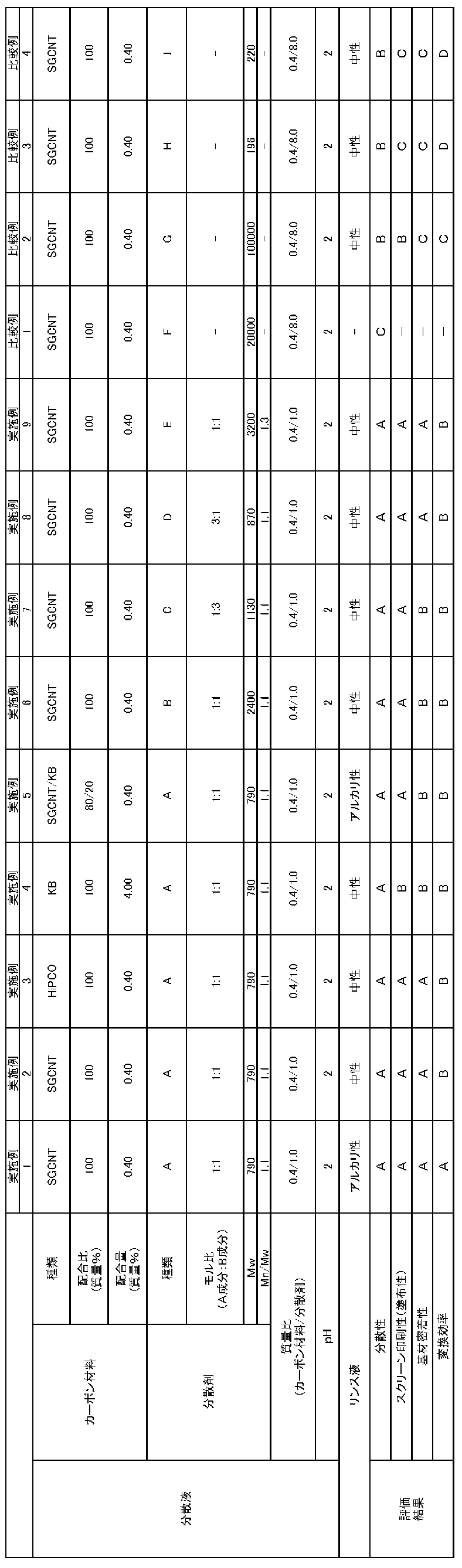
表1より、実施例1~9の分散液を用いれば、基材に対する塗布性(濡れ性)を向上させる(スクリーン印刷性を向上させる)ことができ、基材との密着性が高い導電膜を形成することができることが分かる。
From Table 1, by using the dispersions of Examples 1 to 9, it is possible to improve the coating property (wettability) on the substrate (improve the screen printability), and the conductive film having high adhesion to the substrate. It can be seen that can be formed.
本発明によれば、基材に対する塗布性(濡れ性)を向上させることができ、基材との密着性が高い導電膜を形成することができる分散液を提供することができる。
また、本発明によれば、基材との密着性が高い導電膜およびその製造方法、該導電膜を備え、高い導電性を有する電極、並びに、該電極を備え、高い変換効率を有する太陽電池を提供することができる。 According to the present invention, it is possible to provide a dispersion liquid capable of improving the coating property (wettability) with respect to a substrate and forming a conductive film having high adhesion to the substrate.
Further, according to the present invention, a conductive film having high adhesion to a base material, a method for producing the conductive film, an electrode having the conductive film and having high conductivity, and a solar cell having the electrode and having high conversion efficiency. Can be provided.
また、本発明によれば、基材との密着性が高い導電膜およびその製造方法、該導電膜を備え、高い導電性を有する電極、並びに、該電極を備え、高い変換効率を有する太陽電池を提供することができる。 According to the present invention, it is possible to provide a dispersion liquid capable of improving the coating property (wettability) with respect to a substrate and forming a conductive film having high adhesion to the substrate.
Further, according to the present invention, a conductive film having high adhesion to a base material, a method for producing the conductive film, an electrode having the conductive film and having high conductivity, and a solar cell having the electrode and having high conversion efficiency. Can be provided.
1 第1基材
2 光電極
3 第1基板
4 電解質層
5 第2基材
6 対向電極
7 第2基板
8 隔壁
9 セル接続部(導電性樹脂組成物)
12A 第1取り出し電極
12B 第2取り出し電極
21 光電極用導電層
22 多孔質半導体微粒子層
61 対向電極用導電層
62 触媒層
100 DSCモジュール DESCRIPTION OF SYMBOLS 1 1st base material 2Photoelectrode 3 1st substrate 4 Electrolyte layer 5 2nd base material 6 Counter electrode 7 2nd substrate 8 Partition 9 Cell connection part (electroconductive resin composition)
12A 1st take-outelectrode 12B 2nd take-out electrode 21 Conductive layer 22 for photoelectrodes Porous semiconductor fine particle layer 61 Conductive layer 62 for counter electrodes Catalytic layer 100 DSC module
2 光電極
3 第1基板
4 電解質層
5 第2基材
6 対向電極
7 第2基板
8 隔壁
9 セル接続部(導電性樹脂組成物)
12A 第1取り出し電極
12B 第2取り出し電極
21 光電極用導電層
22 多孔質半導体微粒子層
61 対向電極用導電層
62 触媒層
100 DSCモジュール DESCRIPTION OF SYMBOLS 1 1st base material 2
12A 1st take-out
Claims (13)
- カーボン材料(A)、芳香族スルホン酸化合物とヒドロキシフェノール化合物とアルデヒド化合物との縮合物(B)、および溶媒(C)を含む、分散液。 A dispersion liquid containing a carbon material (A), a condensate of an aromatic sulfonic acid compound, a hydroxyphenol compound and an aldehyde compound (B), and a solvent (C).
- 前記縮合物(B)中における、芳香族スルホン酸化合物に由来する芳香族スルホン酸化合物単量体単位に対するヒドロキシフェノール化合物に由来するヒドロキシフェノール化合物単量体単位のモル比(ヒドロキシフェノール化合物単量体単位/芳香族スルホン酸化合物単量体単位)が1/9以上9/1以下である、請求項1に記載の分散液。 The molar ratio of the hydroxyphenol compound monomer unit derived from the hydroxyphenol compound to the aromatic sulfonic acid compound monomer unit derived from the aromatic sulfonic acid compound in the condensate (B) (hydroxyphenol compound monomer The dispersion according to claim 1, wherein the ratio (unit/aromatic sulfonic acid compound monomer unit) is 1/9 or more and 9/1 or less.
- 前記縮合物(B)の重量平均分子量(標準ポリエチレングリコール換算)が500以上100000以下である、請求項1または2に記載の分散液。 The dispersion according to claim 1 or 2, wherein the condensate (B) has a weight average molecular weight (converted to standard polyethylene glycol) of 500 or more and 100,000 or less.
- 前記縮合物(B)がレゾール型である、請求項1~3のいずれかに記載の分散液。 The dispersion according to any one of claims 1 to 3, wherein the condensate (B) is a resol type.
- 前記縮合物(B)が、下記一般式(1)または下記一般式(2)で表される、請求項1~4のいずれかに記載の分散液。

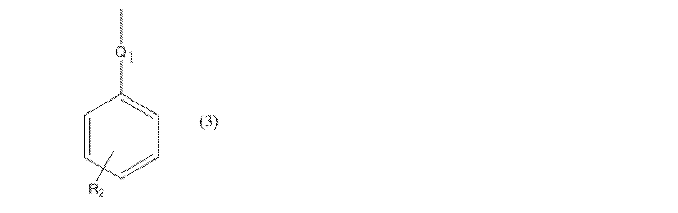
- 前記一般式(3)におけるQがスルホニル基である、請求項5に記載の分散液。 The dispersion according to claim 5, wherein Q in the general formula (3) is a sulfonyl group.
- 前記カーボン材料(A)が繊維状炭素ナノ構造体である、請求項1~6のいずれかに記載の分散液。 The dispersion according to any one of claims 1 to 6, wherein the carbon material (A) is a fibrous carbon nanostructure.
- 前記溶媒(C)が水を含み、前記分散液のpHが7未満である、請求項1~7のいずれかに記載の分散液。 The dispersion according to any one of claims 1 to 7, wherein the solvent (C) contains water and the pH of the dispersion is less than 7.
- 前記カーボン材料(A)100質量部当たり、前記縮合物(B)を50質量部以上500質量部以下含む、請求項1~8のいずれかに記載の分散液。 The dispersion according to any one of claims 1 to 8, which contains 50 parts by mass or more and 500 parts by mass or less of the condensate (B) per 100 parts by mass of the carbon material (A).
- 請求項1~9のいずれかに記載の分散液を用いて得られる導電膜。 A conductive film obtained by using the dispersion according to any one of claims 1 to 9.
- 請求項10に記載の導電膜を備える電極。 An electrode provided with the conductive film according to claim 10.
- 請求項11に記載の電極を備える太陽電池。 A solar cell provided with the electrode according to claim 11.
- 請求項1~9いずれかに記載の分散液を基材上に塗布し乾燥させて導電膜を形成する工程(1)と、
前記工程(1)で得られた導電膜を溶媒で洗浄し、前記導電膜から前記縮合物(B)の少なくとも一部を除去する工程(2)と、
を含む、導電膜の製造方法。 A step (1) of forming a conductive film by applying the dispersion according to any one of claims 1 to 9 onto a base material and drying the dispersion.
A step (2) of washing the conductive film obtained in the step (1) with a solvent to remove at least part of the condensate (B) from the conductive film;
A method of manufacturing a conductive film, comprising:
Priority Applications (4)
| Application Number | Priority Date | Filing Date | Title |
|---|---|---|---|
| CN202080009731.6A CN113330066B (en) | 2019-02-01 | 2020-01-21 | Dispersion, conductive film, method for producing same, electrode, and solar cell |
| US17/424,163 US20220098354A1 (en) | 2019-02-01 | 2020-01-21 | Dispersion liquid, conductive film and production method thereof, electrode, and solar cell |
| JP2020569534A JPWO2020158507A1 (en) | 2019-02-01 | 2020-01-21 | Dispersion liquid, conductive film and its manufacturing method, electrodes, and solar cells |
| EP20749148.1A EP3919560A4 (en) | 2019-02-01 | 2020-01-21 | Dispersion liquid, conductive film and method for producing same, electrode, and solar cell |
Applications Claiming Priority (2)
| Application Number | Priority Date | Filing Date | Title |
|---|---|---|---|
| JP2019017429 | 2019-02-01 | ||
| JP2019-017429 | 2019-02-01 |
Publications (1)
| Publication Number | Publication Date |
|---|---|
| WO2020158507A1 true WO2020158507A1 (en) | 2020-08-06 |
Family
ID=71840895
Family Applications (1)
| Application Number | Title | Priority Date | Filing Date |
|---|---|---|---|
| PCT/JP2020/001921 WO2020158507A1 (en) | 2019-02-01 | 2020-01-21 | Dispersion liquid, conductive film and method for producing same, electrode, and solar cell |
Country Status (6)
| Country | Link |
|---|---|
| US (1) | US20220098354A1 (en) |
| EP (1) | EP3919560A4 (en) |
| JP (1) | JPWO2020158507A1 (en) |
| CN (1) | CN113330066B (en) |
| TW (1) | TW202040595A (en) |
| WO (1) | WO2020158507A1 (en) |
Cited By (1)
| Publication number | Priority date | Publication date | Assignee | Title |
|---|---|---|---|---|
| WO2022064939A1 (en) * | 2020-09-24 | 2022-03-31 | 日本ゼオン株式会社 | Carbon nanotube aqueous dispersion, conductive film, electrode, and solar cell and method for producing same |
Families Citing this family (1)
| Publication number | Priority date | Publication date | Assignee | Title |
|---|---|---|---|---|
| CN115182021A (en) * | 2021-04-01 | 2022-10-14 | 浙江正泰电器股份有限公司 | Composite dispersant and mixed electroplating solution |
Citations (17)
| Publication number | Priority date | Publication date | Assignee | Title |
|---|---|---|---|---|
| US3219607A (en) * | 1961-02-21 | 1965-11-23 | Kuhlmann Ets | Aqueous dispersions of vinyl chloride-acrylic ester copolymers emulsified with sulfonated phenol aldehyde condensates |
| CS214121B1 (en) * | 1980-05-30 | 1982-04-09 | Vlastimil Fiedler | Method for the production of negative electrodes of lead accumulators |
| WO2005031204A2 (en) * | 2003-09-24 | 2005-04-07 | Terramix, S.A. | Protective coating compositions and techniques for fluid piping systems |
| WO2006011655A1 (en) | 2004-07-27 | 2006-02-02 | National Institute Of Advanced Industrial Scienceand Technology | Single-layer carbon nanotube and alinged single-layer carbon nanotube bulk structure, and their production process, production apparatus and use |
| CN101274831A (en) * | 2008-05-16 | 2008-10-01 | 哈尔滨工业大学 | Carbon nano-tube fiber cement-based material and preparation thereof |
| JP2009163959A (en) | 2007-12-28 | 2009-07-23 | Toray Ind Inc | Transparent conductive film, and manufacturing method thereof |
| WO2011108175A1 (en) * | 2010-03-02 | 2011-09-09 | 新神戸電機株式会社 | Lead storage battery |
| WO2012042917A1 (en) * | 2010-09-30 | 2012-04-05 | 新神戸電機株式会社 | Lead storage battery |
| CN102924020A (en) * | 2012-10-26 | 2013-02-13 | 青岛理工大学 | Piezoresistance/piezoelectric composite material, manufacturing method of material, sensor utilizing material and manufacturing method of sensor |
| WO2013042482A1 (en) | 2011-09-20 | 2013-03-28 | 東ソー有機化学株式会社 | Polystyrene sulfonate copolymer, dispersant using same, aqueous nanocarbon material dispersion, and method for producing polystyrene sulfonate copolymer |
| JP2013199419A (en) | 2012-02-23 | 2013-10-03 | Toray Ind Inc | Carbon nanotube dispersion |
| JP2014049631A (en) | 2012-08-31 | 2014-03-17 | Peccell Technologies Inc | Photoelectric conversion element using perovskite compound and method of manufacturing the same |
| JP2015046583A (en) | 2013-07-31 | 2015-03-12 | 富士フイルム株式会社 | Photoelectric conversion element, and solar cell |
| WO2015115102A1 (en) | 2014-01-31 | 2015-08-06 | 日本ゼオン株式会社 | Carbon nanotube dispersion liquid, conductor film and conductive film |
| WO2015156293A1 (en) * | 2014-04-08 | 2015-10-15 | 日立化成株式会社 | Bisphenol-based resin, electrode, lead storage battery, production methods for these, and resin composition |
| JP2016009737A (en) | 2014-06-24 | 2016-01-18 | 株式会社リコー | Method for manufacturing perovskite type solar battery |
| JP2017160326A (en) * | 2016-03-09 | 2017-09-14 | 日立化成株式会社 | Phenolic resin, electrode, lead storage battery and method of producing the same, and resin composition |
Family Cites Families (7)
| Publication number | Priority date | Publication date | Assignee | Title |
|---|---|---|---|---|
| JP5621841B2 (en) * | 2010-03-01 | 2014-11-12 | 新神戸電機株式会社 | Lead acid battery |
| WO2012086008A1 (en) * | 2010-12-21 | 2012-06-28 | 新神戸電機株式会社 | Lead storage battery |
| JP5445655B2 (en) * | 2012-10-25 | 2014-03-19 | 新神戸電機株式会社 | Lead acid battery |
| KR101771506B1 (en) * | 2013-08-27 | 2017-08-25 | 닛산 가가쿠 고교 가부시키 가이샤 | Agent for dispersing electrically conductive carbon material, and dispersion of electrically conductive carbon material |
| JP6222239B2 (en) * | 2013-10-28 | 2017-11-01 | 日立化成株式会社 | Resin composition, electrode, lead-acid battery, and production method thereof |
| JP6202197B2 (en) * | 2014-04-22 | 2017-09-27 | 日立化成株式会社 | Bisphenol resin, resin composition, electrode layer, electrode and lead acid battery |
| EP3188289A4 (en) * | 2014-08-27 | 2018-03-07 | Hitachi Chemical Company, Ltd. | Lead storage battery |
-
2020
- 2020-01-21 WO PCT/JP2020/001921 patent/WO2020158507A1/en unknown
- 2020-01-21 EP EP20749148.1A patent/EP3919560A4/en active Pending
- 2020-01-21 US US17/424,163 patent/US20220098354A1/en active Pending
- 2020-01-21 CN CN202080009731.6A patent/CN113330066B/en active Active
- 2020-01-21 JP JP2020569534A patent/JPWO2020158507A1/en active Pending
- 2020-01-22 TW TW109102613A patent/TW202040595A/en unknown
Patent Citations (17)
| Publication number | Priority date | Publication date | Assignee | Title |
|---|---|---|---|---|
| US3219607A (en) * | 1961-02-21 | 1965-11-23 | Kuhlmann Ets | Aqueous dispersions of vinyl chloride-acrylic ester copolymers emulsified with sulfonated phenol aldehyde condensates |
| CS214121B1 (en) * | 1980-05-30 | 1982-04-09 | Vlastimil Fiedler | Method for the production of negative electrodes of lead accumulators |
| WO2005031204A2 (en) * | 2003-09-24 | 2005-04-07 | Terramix, S.A. | Protective coating compositions and techniques for fluid piping systems |
| WO2006011655A1 (en) | 2004-07-27 | 2006-02-02 | National Institute Of Advanced Industrial Scienceand Technology | Single-layer carbon nanotube and alinged single-layer carbon nanotube bulk structure, and their production process, production apparatus and use |
| JP2009163959A (en) | 2007-12-28 | 2009-07-23 | Toray Ind Inc | Transparent conductive film, and manufacturing method thereof |
| CN101274831A (en) * | 2008-05-16 | 2008-10-01 | 哈尔滨工业大学 | Carbon nano-tube fiber cement-based material and preparation thereof |
| WO2011108175A1 (en) * | 2010-03-02 | 2011-09-09 | 新神戸電機株式会社 | Lead storage battery |
| WO2012042917A1 (en) * | 2010-09-30 | 2012-04-05 | 新神戸電機株式会社 | Lead storage battery |
| WO2013042482A1 (en) | 2011-09-20 | 2013-03-28 | 東ソー有機化学株式会社 | Polystyrene sulfonate copolymer, dispersant using same, aqueous nanocarbon material dispersion, and method for producing polystyrene sulfonate copolymer |
| JP2013199419A (en) | 2012-02-23 | 2013-10-03 | Toray Ind Inc | Carbon nanotube dispersion |
| JP2014049631A (en) | 2012-08-31 | 2014-03-17 | Peccell Technologies Inc | Photoelectric conversion element using perovskite compound and method of manufacturing the same |
| CN102924020A (en) * | 2012-10-26 | 2013-02-13 | 青岛理工大学 | Piezoresistance/piezoelectric composite material, manufacturing method of material, sensor utilizing material and manufacturing method of sensor |
| JP2015046583A (en) | 2013-07-31 | 2015-03-12 | 富士フイルム株式会社 | Photoelectric conversion element, and solar cell |
| WO2015115102A1 (en) | 2014-01-31 | 2015-08-06 | 日本ゼオン株式会社 | Carbon nanotube dispersion liquid, conductor film and conductive film |
| WO2015156293A1 (en) * | 2014-04-08 | 2015-10-15 | 日立化成株式会社 | Bisphenol-based resin, electrode, lead storage battery, production methods for these, and resin composition |
| JP2016009737A (en) | 2014-06-24 | 2016-01-18 | 株式会社リコー | Method for manufacturing perovskite type solar battery |
| JP2017160326A (en) * | 2016-03-09 | 2017-09-14 | 日立化成株式会社 | Phenolic resin, electrode, lead storage battery and method of producing the same, and resin composition |
Non-Patent Citations (1)
| Title |
|---|
| See also references of EP3919560A4 |
Cited By (1)
| Publication number | Priority date | Publication date | Assignee | Title |
|---|---|---|---|---|
| WO2022064939A1 (en) * | 2020-09-24 | 2022-03-31 | 日本ゼオン株式会社 | Carbon nanotube aqueous dispersion, conductive film, electrode, and solar cell and method for producing same |
Also Published As
| Publication number | Publication date |
|---|---|
| EP3919560A4 (en) | 2022-10-26 |
| CN113330066A (en) | 2021-08-31 |
| JPWO2020158507A1 (en) | 2021-12-09 |
| EP3919560A1 (en) | 2021-12-08 |
| CN113330066B (en) | 2024-01-30 |
| TW202040595A (en) | 2020-11-01 |
| US20220098354A1 (en) | 2022-03-31 |
Similar Documents
| Publication | Publication Date | Title |
|---|---|---|
| RU2578664C2 (en) | Transparent conducting large-area coatings, including doped carbon nanotubes and nano-wire composite materials, and methods for obtaining thereof | |
| Zhu et al. | Anthocyanin-sensitized solar cells using carbon nanotube films as counter electrodes | |
| EP2543087B1 (en) | Electronic devices including transparent conductive coatings including carbon nanotubes and nanowire composites | |
| JP5690852B2 (en) | Method for producing coated article comprising alloyed carbon nanotube thin film | |
| KR20160060042A (en) | Carbon nanotubes, dispersion liquid thereof, carbon nanotube-containing film and composition material | |
| WO2020158507A1 (en) | Dispersion liquid, conductive film and method for producing same, electrode, and solar cell | |
| Shiraz et al. | Carbonaceous materials as substitutes for conventional dye-sensitized solar cell counter electrodes | |
| US20190066933A1 (en) | Transparent conductive film, photoelectrode for dye-sensitized solar cell, touch panel, and dye-sensitized solar cell | |
| WO2021106660A1 (en) | Carbon nanotube aqueous dispersion, conductive film, electrode, and solar cell | |
| JP6783998B2 (en) | Method for manufacturing laminate for organic-inorganic composite solar cell and method for manufacturing organic-inorganic composite solar cell | |
| WO2020158370A1 (en) | Conductive film, method for producing same, electrode and solar cell | |
| WO2022064939A1 (en) | Carbon nanotube aqueous dispersion, conductive film, electrode, and solar cell and method for producing same | |
| WO2023026764A1 (en) | Electrically conductive composition for solar cell, electrode for solar cell, solar cell, and solar cell module | |
| JP7276364B2 (en) | Counter electrode for photoelectric conversion element, dye-sensitized solar cell and solar cell module | |
| WO2023085215A1 (en) | Solar cell electrode, solar cell, and solar cell module | |
| JP6911833B2 (en) | Electrodes for solar cells, their manufacturing methods, and solar cells | |
| JP6135166B2 (en) | Redox catalyst, electrode material, electrode, solar cell, fuel cell, and nitrogen oxide removal catalyst | |
| JP6613556B2 (en) | Conductive composition, dye-sensitized solar cell electrode and method for producing the same, and dye-sensitized solar cell | |
| JP2020123480A (en) | Method for producing conductive film, method for producing counter electrode for dye-sensitized solar cell, method for producing photoelectrode for dye-sensitized solar cell, and method for producing wiring |
Legal Events
| Date | Code | Title | Description |
|---|---|---|---|
| 121 | Ep: the epo has been informed by wipo that ep was designated in this application |
Ref document number: 20749148 Country of ref document: EP Kind code of ref document: A1 |
|
| ENP | Entry into the national phase |
Ref document number: 2020569534 Country of ref document: JP Kind code of ref document: A |
|
| NENP | Non-entry into the national phase |
Ref country code: DE |
|
| ENP | Entry into the national phase |
Ref document number: 2020749148 Country of ref document: EP Effective date: 20210901 |