WO2020157958A1 - スピン軌道トルク型磁気抵抗効果素子及び磁気メモリ - Google Patents
スピン軌道トルク型磁気抵抗効果素子及び磁気メモリ Download PDFInfo
- Publication number
- WO2020157958A1 WO2020157958A1 PCT/JP2019/003628 JP2019003628W WO2020157958A1 WO 2020157958 A1 WO2020157958 A1 WO 2020157958A1 JP 2019003628 W JP2019003628 W JP 2019003628W WO 2020157958 A1 WO2020157958 A1 WO 2020157958A1
- Authority
- WO
- WIPO (PCT)
- Prior art keywords
- orbit torque
- spin orbit
- magnetoresistive effect
- spin
- type magnetoresistive
- Prior art date
- Legal status (The legal status is an assumption and is not a legal conclusion. Google has not performed a legal analysis and makes no representation as to the accuracy of the status listed.)
- Ceased
Links
Images





Classifications
-
- H—ELECTRICITY
- H10—SEMICONDUCTOR DEVICES; ELECTRIC SOLID-STATE DEVICES NOT OTHERWISE PROVIDED FOR
- H10B—ELECTRONIC MEMORY DEVICES
- H10B61/00—Magnetic memory devices, e.g. magnetoresistive RAM [MRAM] devices
- H10B61/20—Magnetic memory devices, e.g. magnetoresistive RAM [MRAM] devices comprising components having three or more electrodes, e.g. transistors
- H10B61/22—Magnetic memory devices, e.g. magnetoresistive RAM [MRAM] devices comprising components having three or more electrodes, e.g. transistors of the field-effect transistor [FET] type
-
- H—ELECTRICITY
- H10—SEMICONDUCTOR DEVICES; ELECTRIC SOLID-STATE DEVICES NOT OTHERWISE PROVIDED FOR
- H10N—ELECTRIC SOLID-STATE DEVICES NOT OTHERWISE PROVIDED FOR
- H10N52/00—Hall-effect devices
- H10N52/80—Constructional details
-
- H—ELECTRICITY
- H10—SEMICONDUCTOR DEVICES; ELECTRIC SOLID-STATE DEVICES NOT OTHERWISE PROVIDED FOR
- H10N—ELECTRIC SOLID-STATE DEVICES NOT OTHERWISE PROVIDED FOR
- H10N50/00—Galvanomagnetic devices
- H10N50/10—Magnetoresistive devices
-
- H—ELECTRICITY
- H10—SEMICONDUCTOR DEVICES; ELECTRIC SOLID-STATE DEVICES NOT OTHERWISE PROVIDED FOR
- H10N—ELECTRIC SOLID-STATE DEVICES NOT OTHERWISE PROVIDED FOR
- H10N52/00—Hall-effect devices
- H10N52/101—Semiconductor Hall-effect devices
Definitions
- the present invention relates to a spin orbit torque type magnetoresistive effect element and a magnetic memory.
- the magnetoresistive effect element is expected to be applied to magnetic sensors, high-frequency components, magnetic heads, and nonvolatile random access memory (MRAM).
- MRAM nonvolatile random access memory
- the magnetoresistive effect element outputs the change in the mutual magnetization directions of the two ferromagnetic layers sandwiching the non-magnetic layer as the change in resistance of the element.
- the magnetoresistive element records the data by controlling the magnetization direction of the ferromagnetic layer.
- Known methods for controlling the direction of magnetization include a method using a magnetic field generated by a current and a method using spin transfer torque (STT) generated when a current is passed in the stacking direction of the magnetoresistive effect element. In the method using STT, it is necessary to apply a potential difference in the direction of penetrating the nonmagnetic layer, which may damage the nonmagnetic layer.
- SOT spin orbit torque
- Patent Document 1 a method using spin orbit torque (SOT) has been studied as a new method for controlling the direction of magnetization.
- SOT is induced in the ferromagnetic layer by the spin current generated by the spin-orbit interaction or the Rashba effect at the interface between different materials.
- the SOT acts on the magnetization in the ferromagnetic layer and reverses the magnetization of the ferromagnetic layer.
- the spin current and the Rashba effect occur when a current flows in a direction intersecting the stacking direction of the ferromagnetic layers.
- the method using the SOT can prevent a large write current from flowing in the stacking direction of the nonmagnetic layer and the ferromagnetic layer, and can suppress damage to the nonmagnetic layer and the like.
- the magnetoresistive effect element is a recording area for recording data, and is often used as a magnetic memory in which a plurality of magnetoresistive effect elements are integrated. In order to reduce the size of the entire magnetic memory, it is required to enhance the integration of the magnetoresistive effect element.
- the present invention has been made in view of the above circumstances, and an object of the present invention is to provide a spin-orbit torque type magnetoresistive effect element capable of improving integration. Another object is to provide a magnetic memo having a high degree of integration.
- the present invention provides the following means in order to solve the above problems.
- the spin-orbit torque type magnetoresistive effect element includes a first ferromagnetic layer, a second ferromagnetic layer, and between the first ferromagnetic layer and the second ferromagnetic layer.
- the gate insulating layer and the gate are located between the conductive portion and the second surface of the spin orbit torque wiring, which faces the first surface of the spin orbit torque wiring opposite to the first surface, and is close to the spin orbit torque wiring.
- a gate portion having an electrode, and the spin orbit torque wiring includes a semiconductor.
- the spin-orbit torque type magnetoresistive effect element according to the above aspect is electrically connected to the second ferromagnetic layer of the element section and electrically connected to the element section by the via wiring extending in the first direction. And a first transistor connected to.
- the semiconductor forming the spin-orbit torque wiring may be any one selected from the group consisting of Si, SiGe, GaAs, Ge and InGaAs. Good.
- the spin-orbit torque wiring may include a scattering element.
- the scattering element may be a heavy metal element having an atomic number of yttrium or more.
- the scattering element may be a magnetic element.
- the magnetic memory according to the second aspect includes a plurality of spin orbit torque type magnetoresistive effect elements according to the above aspect.
- the plurality of spin orbit torque type magnetoresistive effect elements have a first element row in which the spin orbit torque type magnetoresistive effect elements are arranged in the second direction, and In the first element row, the two spin orbit torque type magnetoresistive effect elements adjacent to each other in the second direction have the second conductive portion of one of the spin orbit torque type magnetoresistive effect elements and the other spin orbit. It is shared as the first conductive portion of the torque type magnetoresistive effect element.
- the plurality of spin orbit torque type magnetoresistive effect elements have a first element row in which the spin orbit torque type magnetoresistive effect elements are arranged in the second direction, and
- the spin orbit torque wirings of the plurality of spin orbit torque type magnetoresistive effect elements forming the first element row may be connected to each other.
- the spin orbit torque type magnetoresistive effect elements are arranged in a third direction different from the first direction and the second direction.
- the respective second conductive portions of the spin orbit torque type magnetoresistive effect element may be connected to each other.
- the integration of the element can be enhanced. Further, the magnetic memory according to the above aspect can be miniaturized.
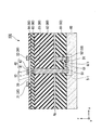
- FIG. 3 is a cross-sectional view of a main part of the spin orbit torque type magnetoresistive effect element according to the first embodiment.
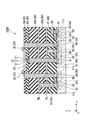
- FIG. 3 is a cross-sectional view of the spin orbit torque type magnetoresistive effect element according to the first embodiment.
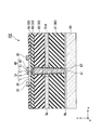
- FIG. 6 is a cross-sectional view of a spin orbit torque type magnetoresistive effect element having no gate portion.
- FIG. 7 is a sectional view of a first modification of the spin orbit torque type magnetoresistive effect element according to the first embodiment.
- FIG. 6 is a cross-sectional view of a second modification of the spin orbit torque type magnetoresistive effect element according to the first embodiment. It is a perspective view of a part of magnetic memory concerning 2nd Embodiment.
- FIG. 6 is a cross-sectional view of a spin orbit torque type magnetoresistive effect element that constitutes a magnetic memory according to a second embodiment.
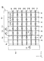
- FIG. 9 is a circuit diagram for explaining a data write operation of the magnetic memory according to the second embodiment.
- FIG. 9 is a circuit diagram for explaining a data read operation from the magnetic memory according to the second embodiment.
- FIG. 9 is a circuit diagram for explaining another example of the data writing operation of the magnetic memory according to the second embodiment. It is a circuit diagram of a modification of the magnetic memory according to the second embodiment.
- the z direction is the direction in which the spin orbit torque wiring 20 is located with respect to the element unit 10 described later.
- the x direction is the direction in which the spin orbit torque wiring, which will be described later, extends.
- the y direction is a direction orthogonal to the x direction and the z direction.
- the z direction is an example of the first direction
- the x direction is an example of the second direction
- the y direction is an example of the third direction.
- “extending in the x direction” means, for example, that the dimension in the x direction is larger than the minimum dimension among the dimensions in the x direction, the y direction, and the z direction. The same applies when extending in other directions.
- FIG. 1 is a sectional view of a main portion of a spin orbit torque type magnetoresistive effect element according to the first embodiment.
- FIG. 2 is a sectional view of the spin orbit torque type magnetoresistive effect element according to the first embodiment. 1 and 2 are cross sections taken along the xz plane that passes through the center of the spin orbit torque wiring 20 to be described later in the y direction.
- the spin orbit torque type magnetoresistive effect element 100 includes an element portion 10, a spin orbit torque wiring 20, a plurality of conductive portions 30, a gate portion 40, a plurality of via wirings 50, a substrate 60, and an insulating layer 80. , And the read wiring Rp.
- the element unit 10 has a first ferromagnetic layer 1, a second ferromagnetic layer 2, and a nonmagnetic layer 3.
- the element unit 10 faces the first surface 20 a of the spin orbit torque wiring 20.
- “facing” means a relationship facing each other, and two layers may be in contact with each other or may have another layer between them.
- the element unit 10 is a magnetoresistive element in which the resistance value in the z direction changes based on the difference in relative angle between the magnetization of the first ferromagnetic layer 1 and the magnetization of the second ferromagnetic layer 2.
- the element unit 10 is, for example, a columnar body.
- the shape of the element unit 10 when viewed from the z direction is not particularly limited.
- the element unit 10 has, for example, a circular shape, a quadrangular shape, or an oval shape when viewed from the z direction.
- the widths of the element portion 10 in the x direction and the y direction may be constant or may change in the z direction.
- the widths of the element unit 10 in the x direction and the y direction may increase or decrease with increasing distance from the spin orbit torque wiring 20.
- the first ferromagnetic layer 1 contains a ferromagnetic material, especially a soft magnetic material.
- the first ferromagnetic layer 1 may be referred to as a magnetization free layer.
- the first ferromagnetic layer 1 is, for example, a metal selected from the group consisting of Cr, Mn, Co, Fe, and Ni, an alloy containing at least one of these metals, and at least these metals and B, C, and N. It includes an alloy containing one or more elements.
- the first ferromagnetic layer 1 is, for example, Co-Fe, Co-Fe-B, Ni-Fe, Co-Ho alloy, Sm-Fe alloy, Fe-Pt alloy, Co-Pt alloy, CoCrPt alloy.
- the first ferromagnetic layer 1 may include a Heusler alloy such as Co 2 FeSi.
- Heusler alloys include intermetallic compounds having a chemical composition of XYZ or X 2 YZ.
- X is a transition metal element or noble metal element of Co, Fe, Ni, or Cu group on the periodic table
- Y is a transition metal of Mn, V, Cr, or Ti group or element species of X
- Z is Group III.
- To V are typical elements of group V.
- the Heusler alloy is, for example, Co 2 FeSi, Co 2 FeGe, Co 2 FeGa, Co 2 MnSi, Co 2 Mn 1-a Fe a Al b Si 1-b , Co 2 FeGe 1-c Ga c, or the like. Heusler alloys have a high spin polarizability.
- the first ferromagnetic layer 1 has an easy axis of magnetization either in the xy plane or in the z direction.
- the first ferromagnetic layer 1 has an easy axis of magnetization in any direction in the xy plane, the first ferromagnetic layer 1 is called an in-plane magnetized film.
- the first ferromagnetic layer 1 has an easy axis of magnetization in the z direction, the first ferromagnetic layer 1 is called a perpendicular magnetization film.
- the second ferromagnetic layer 2 is located so as to sandwich the first ferromagnetic layer 1 and the nonmagnetic layer 3.
- the second ferromagnetic layer 2 includes a ferromagnetic material.
- the ferromagnetic material forming the second ferromagnetic layer 2 for example, the same material as that of the first ferromagnetic layer 1 is used.
- the magnetization of the second ferromagnetic layer 2 is less likely to move in a given environment than the magnetization of the first ferromagnetic layer 1.
- the second ferromagnetic layer 2 may be referred to as a magnetization fixed layer.
- the second ferromagnetic layer 2 for example, the second ferromagnetic layer 2 is made of one ferromagnetic material.
- the material forming the second ferromagnetic layer 2 is selected so that the coercive force is higher than that of the first ferromagnetic layer 1.
- the second ferromagnetic layer 2 has a first layer, a second layer and a third layer.
- the first layer and the second layer are made of a ferromagnetic material and are antiferromagnetically coupled to each other.
- the third layer is a non-magnetic body sandwiched between the first layer and the second layer.
- the first layer and the second layer are made of the same material as that of the first ferromagnetic layer 1.
- the third layer is made of, for example, Ru. Due to the antiferromagnetic coupling between the first layer and the second layer, the coercive force of the entire second ferromagnetic layer 2 becomes larger than the coercive force of the first ferromagnetic layer 1.
- the non-magnetic layer 3 is located between the first ferromagnetic layer 1 and the second ferromagnetic layer 2.
- the non-magnetic layer 3 is made of a non-magnetic insulator, semiconductor or metal.
- the element unit 10 is a tunnel magnetic effect (TMR) element.
- TMR tunnel magnetic effect
- the nonmagnetic layer 3 is made of a semiconductor or a metal
- the element unit 10 is a giant magnetoresistive (GMR) element.
- the non-magnetic insulator is, for example, Al 2 O 3 , SiO 2 , MgO, MgAl 2 O 4 , or a material in which some of Al, Ga, Si, and Mg are replaced with Zn, Be, or the like.
- the nonmagnetic layer 3 is made of a nonmagnetic insulator, the nonmagnetic layer 3 is a tunnel barrier layer. MgO or MgAl 2 O 4 easily realizes a coherent tunnel between the first ferromagnetic layer 1 and the second ferromagnetic layer 2.
- the non-magnetic metal is, for example, Cu, Au, Ag or the like.
- the non-magnetic semiconductor is, for example, Si, Ge, Si-Ge, CuInSe 2 , CuGaSe 2 , Cu(In,Ga)Se 2 or the like.
- the element unit 10 may have layers other than the first ferromagnetic layer 1, the second ferromagnetic layer 2, and the nonmagnetic layer 3.
- the spin orbit torque wiring 20 is located in the z direction of the element unit 10.
- the spin orbit torque wiring 20 faces the first ferromagnetic layer 1 of the element unit 10.
- the spin orbit torque wiring 20 extends in the x direction across the two conductive parts 30 when viewed from the z direction.
- a current I flows along the spin orbit torque wiring 20.
- the first spin s1 oriented in one direction and the second spin s2 oriented in the opposite direction to the first spin s1 are respectively bent in a direction orthogonal to the current.
- the first spin s1 oriented in the +y direction is bent in the +z direction
- the second spin s2 oriented in the ⁇ y direction is bent in the ⁇ z direction.
- the ordinary Hall effect and spin Hall effect are common in that the moving (moving) charge (electron) can bend the moving (moving) direction.
- the ordinary Hall effect charged particles moving in a magnetic field are bent by the Lorentz force, and the spin Hall effect causes electrons to move (current The difference is that the moving direction of the spin can be bent only by.
- the number of electrons in the first spin s1 and the number of electrons in the second spin s2 generated by the spin Hall effect are equal.
- the number of electrons of the first spin s1 toward the +z direction and the number of electrons of the second spin s2 toward the ⁇ z direction are equal.
- the spin current without an electric current is particularly called a pure spin current.
- the spin orbit torque wiring 20 faces the element unit 10.
- Spin is injected from the spin orbit torque wiring 20 into the first ferromagnetic layer 1 of the element unit 10.
- the injected spin adds a spin orbit torque (SOT) to the magnetization of the first ferromagnetic layer 1.
- SOT spin orbit torque
- the spin orbit torque wiring 20 includes a semiconductor.
- the semiconductor forming the spin-orbit torque wiring 20 is, for example, any one selected from the group consisting of Si, SiGe, GaAs, Ge, and InGaAs.
- the spin orbit torque wiring 20 may be a semiconductor to which a scattering element is added.
- the scattering element is, for example, a heavy metal element having an atomic number of yttrium (Y) or higher.
- the scattering element is also, for example, a magnetic element.
- Semiconductors have smaller spin-orbit interaction than non-magnetic heavy metals, for example.
- the generation efficiency of the spin current is low, but if a current with a large current density is applied to the spin orbit torque wiring 20, the magnetization of the first ferromagnetic layer 1 is reversed. Sufficient torque can be applied to the magnetization of the first ferromagnetic layer 1.
- the scattering element becomes a spin scattering factor.
- the spins moving inside the spin-orbit torque wiring 20 are scattered, the spin-orbit interaction is enhanced, and the spin current generation efficiency with respect to the current density of the current applied to the spin-orbit torque wiring 20 is improved.
- the amount of current applied to the spin orbit torque wiring 20 can be significantly reduced.
- the first ferromagnetic layer 1 A torque sufficient to reverse the magnetization can be applied to the magnetization of the first ferromagnetic layer 1.
- the amount of the scattering element added is, for example, 1 ⁇ 10 13 cm ⁇ 3 or more and 1 ⁇ 10 18 cm ⁇ 3 or less.
- the spin orbit torque wiring 20 behaves like a metal. Further, when the scattering elements increase, the movement of the generated spin current in the z direction may be hindered by the scattering elements, and the spin current generation efficiency may decrease.
- the conductive portion 30 is provided at a position sandwiching the element portion 10 when viewed from the z direction.
- the conductive portion 30 shown in FIG. 1 faces the second surface 20b of the spin orbit torque wiring 20.
- the second surface 20b is a surface opposite to the first surface 20a facing the element unit 10.
- the conductive portion 30 may face the first surface 20a.
- one of the two conductive parts 30 is referred to as a first conductive part 31, and the other is referred to as a second conductive part 32.
- the conductive portion 30 is, for example, a wiring or an electrode.
- the conductive portion 30 is made of a conductive material.
- the conductive portion 30 is, for example, aluminum, copper, or silver.
- the conductive portion 30 shown in FIG. 1 extends in the y direction.
- the gate section 40 is located between the first conductive section 31 and the second conductive section 32 when viewed in the z direction.
- the gate portion 40 faces the second surface 20b of the spin orbit torque wiring 20.
- the gate section 40 faces the element section 10 with the spin orbit torque wiring 20 interposed therebetween, for example.
- the gate portion 40 has a gate insulating layer 41 and a gate electrode 42 from a position close to the spin orbit torque wiring 20.
- the gate insulating layer 41 is, for example, silicon oxide (SiO x ), silicon nitride (SiN x ), silicon carbide (SiC), chromium nitride, silicon carbonitride (SiCN), silicon oxynitride (SiON), aluminum oxide (Al 2 O 3 ) and zirconium oxide (ZrO x ).
- the gate electrode 42 is made of a conductive material.
- the gate electrode 42 is, for example, aluminum, copper, or silver.
- the width of the gate section 40 in the x direction is, for example, wider than the width of the element section 10 in the x direction.
- a voltage is applied to the gate electrode 42, a channel is formed between the first conductive portion 31 and the second conductive portion 32, and the first conductive portion 31 and the second conductive portion 32 are electrically connected.
- the width of the gate portion 40 in the x direction is large, the leakage current between the first conductive portion 31 and the second conductive portion 32 is suppressed.
- the via wiring 50 is located in the first insulating layer 81 and the second insulating layer 82 (see FIG. 2).
- the via wiring 50 is formed in the opening provided in the first insulating layer 81 and the second insulating layer 82.
- the via wiring 50 extends in the z direction, for example.
- the via wiring 50 that electrically connects the second ferromagnetic layer 2 of the element portion 10 and the substrate 60 is referred to as a first via wiring 51
- the via wiring that electrically connects the read wiring Rp and the substrate 60 is referred to as a second via wiring 52.
- the via wiring 50 includes a material having high conductivity.
- the via wiring 50 is, for example, copper, aluminum, silver, a conductive oxide film, a conductive nitride film, or amorphous silicon.
- the substrate 60 is, for example, a semiconductor substrate.
- the substrate 60 is, for example, a silicon substrate.
- the substrate 60 has a source region S1 and a drain region D1.
- the source region S1 and the drain region D1 are regions where impurities are implanted into the substrate 60.
- a first transistor Tr1 is formed near the surface of the substrate 60.
- the first transistor Tr1 has a source region S1, a drain region D1, a gate electrode G1, and a gate insulating layer GI1.
- the first transistor Tr1 is electrically connected to the element unit 10 by the first via wiring 51.
- the gate electrode G1 and the gate insulating layer GI1 are located between the source region S1 and the drain region D1 when viewed from the z direction.
- the gate electrode G1 faces the surface of the substrate 60.
- the gate insulating layer GI1 is located between the substrate 60 and the gate electrode G1.
- the gate electrode G1 is made of the same material as the gate electrode 42, and the gate insulating layer GI1 is made of the same material as the gate insulating layer 41.
- the insulating layer 80 is an insulating layer that insulates between the wirings of the multilayer wiring and between the elements.
- the insulating layer 80 insulates the element unit 10, the first transistor Tr1, and the read wiring Rp except the via wiring 50.
- the insulating layer 80 has, for example, a first insulating layer 81, a second insulating layer 82, a third insulating layer 83, and a fourth insulating layer 84.
- the first insulating layer 81 is located between the substrate 60 and the read wiring Rp.
- the second insulating layer 82 covers the periphery of the first via wiring 51 at a position closer to the element unit 10 than the read wiring Rp.
- the third insulating layer 83 covers the periphery of the element unit 10.
- the fourth insulating layer 84 covers the periphery of the spin orbit torque wiring 20.
- the insulating layer 80 is made of, for example, a material similar to the material used for an interlayer insulating layer of a semiconductor device or the like.
- the insulating layer 80 includes, for example, silicon oxide (SiO x ), silicon nitride (SiN x ), silicon carbide (SiC), chromium nitride, silicon carbonitride (SiCN), silicon oxynitride (SiON), aluminum oxide (Al 2 O). 3 ), zirconium oxide (ZrO x ), and the like.
- the spin orbit torque type magnetoresistive effect element 100 controls the direction of magnetization of the first ferromagnetic layer 1 to write data. Further, the spin-orbit torque magnetoresistive effect element 100 reads, as data, a change in the resistance value of the element unit 10 due to a difference in relative angle between the magnetization of the first ferromagnetic layer 1 and the magnetization of the second ferromagnetic layer 2. ..
- a voltage is first applied to the gate electrode 42. Since the spin orbit torque wiring 20 is a semiconductor, when a voltage is applied to the gate electrode 42, a channel is formed between the first conductive portion 31 and the second conductive portion 32. A channel is a passage for electrons. When the channel is formed between the first conductive portion 31 and the second conductive portion 32, the current I flows in the spin orbit torque wiring 20.
- the first spin s1 and the second spin s2 are unevenly distributed near the surface of the spin orbit torque wiring 20 due to the spin Hall effect.
- a spin current is generated in a direction (z direction) that eliminates uneven distribution of the first spin s1 and the second spin s2.
- a part of the spins in the spin orbit torque wiring 20 is injected into the first ferromagnetic layer 1 of the element unit 10 by the spin current.
- the spin injected into the first ferromagnetic layer 1 gives a spin orbit torque (SOT) to the magnetization of the first ferromagnetic layer 1.
- SOT spin orbit torque
- the magnetization of the first ferromagnetic layer 1 receives a spin orbit torque and rotates (reverses).
- the resistance value of the element unit 10 changes, and data is written in the spin orbit torque type magnetoresistive effect element 100.
- a voltage is applied to the gate electrode G1 of the first transistor Tr1 and the gate electrode 42 of the gate section 40.
- the source region S1 and the drain region D1 are brought into conduction.
- the first conductive portion 31 or the second conductive portion 32 and the element portion 10 are electrically connected.
- conduction is established between these, a current path is formed between the read wiring Rp and the first conductive portion 31 or the second conductive portion 32.
- the resistance value of the spin orbit torque type magnetoresistive effect element 100 is obtained by measuring the potential difference between the read wiring Rp and the first conductive portion 31 or the second conductive portion 32.
- the resistance value of the spin orbit torque type magnetoresistive effect element 100 changes depending on the difference in relative angle of magnetization between the first ferromagnetic layer 1 and the second ferromagnetic layer 2 of the element unit 10. Therefore, the data can be read from the resistance value of the spin orbit torque type magnetoresistive effect element 100.
- the source region S1 and the drain region D1 are formed on the substrate 60.
- the source region S1 and the drain region D1 are formed by a known method.
- a gate insulating layer GI1 and a gate electrode G1 are formed between the source region S1 and the drain region D1.
- the first insulating layer 81 is formed so as to cover the substrate 60, the gate insulating layer GI1, and the gate electrode G1.
- An opening is formed in the first insulating layer 81 from the surface of the first insulating layer 81 toward the drain region D1.
- the opening is filled with a conductor, and the second via wiring 52 is formed.
- One surface of the second via wiring 52 and the first insulating layer 81 is preferably planarized by chemical mechanical polishing (CMP).
- the read wiring Rp and the second insulating layer 82 are formed on one surface of the second via wiring 52 and the first insulating layer 81.
- An opening from the surface of the second insulating layer 82 to the source region S1 is formed in the first insulating layer 81, the read wiring Rp, and the second insulating layer 82.
- the opening is filled with a conductor, and the first via wiring 51 is formed.
- One surface of the first via wiring 51 and the second insulating layer 82 is preferably planarized by chemical mechanical polishing (CMP).
- the element unit 10 is formed at a position overlapping the first via wiring 51 when viewed from the z direction. After forming each layer, the element portion 10 is processed into a predetermined shape by photolithography or the like. Then, the third insulating layer 83 is formed around the element unit 10.
- the spin orbit torque wiring 20 is formed at a position overlapping the element unit 10.
- the spin orbit torque wiring 20 is processed into a predetermined shape by photolithography or the like.
- the fourth insulating layer 84 is formed around the spin orbit torque wiring 20.
- the gate section 40 is formed at a position overlapping with the element section 10 when viewed from the z direction.
- conductive portions 30 are formed on both ends of the spin orbit torque wiring 20.
- Each layer is formed by, for example, a sputtering method, a chemical vapor deposition (CVD) method, or the like.
- the spin orbit torque type magnetoresistive effect element 100 it is possible to improve the integration property when integrating a plurality of elements.
- FIG. 3 is a sectional view of a spin orbit torque type magnetoresistive effect element 100A having no gate portion 40.
- the spin-orbit torque type magnetoresistive element 100A has no gate portion 40, the substrate 61 has a plurality of transistors, the write wiring Wp and the common wiring Cm, and the second insulating layer 82 has the write wiring Wp. 2 is that it is separated into a first portion 82a and a second portion 82b by, and that it has a third via wiring 53, a fourth via wiring 54, a fifth via wiring 55, and a sixth via wiring 56. This is different from the spin orbit torque type magnetoresistive effect element 100 according to the first embodiment shown. The description of the same configuration as the spin orbit torque type magnetoresistive effect element 100 according to the first embodiment is omitted.
- the substrate 61 has a plurality of source regions S1, S2, S3 and a plurality of drain regions D1, D2, D3.
- the plurality of source regions S1, S2, S3 and the plurality of drain regions D1, D2, D3 are regions where impurities are implanted into the substrate 61.
- a first transistor Tr1, a second transistor Tr2, and a third transistor Tr3 are formed near the surface of the substrate 61.
- the second transistor Tr2 has a source region S2, a drain region D2, a gate electrode G2, and a gate insulating layer GI2.
- the third transistor Tr3 has a source region S3, a drain region D3, a gate electrode G3, and a gate insulating layer GI3.
- the third via wiring 53 electrically connects the write wiring Wp and the source region S2.
- the fourth via wiring 54 electrically connects the drain region D2 and the first conductive portion 31.
- the fifth via wiring 55 electrically connects the second conductive portion 32 and the source region S3.
- the sixth via wiring 56 electrically connects the drain region D3 and the common wiring Cm.
- the spin orbit torque type magnetoresistive effect element 100A shown in FIG. 3 controls writing and reading of data by using the three transistors (first transistor Tr1, second transistor Tr2, and third transistor Tr3).
- the area occupied by one transistor in the xy plane is larger than the area occupied by the element unit 10 in the xy plane.
- the spin-orbit torque type magnetoresistive effect element 100A shown in FIG. 3 requires three transistors for controlling data writing and reading. Therefore, the spin orbit torque type magnetoresistive effect element 100A shown in FIG. 3 needs an area for three transistors.
- the spin-orbit torque type magnetoresistive effect element 100 according to the first embodiment shown in FIG. 2 requires only one transistor (first transistor Tr1) for controlling writing and reading of data. Therefore, the spin orbit torque type magnetoresistive effect element 100 shown in FIG. 2 can operate in an area for one transistor, and is excellent in integration.
- FIG. 4 is a sectional view of an essential part of a first modification of the spin orbit torque type magnetoresistive effect element according to the first embodiment.
- the same components as those of the spin orbit torque type magnetoresistive effect element 100 according to the first embodiment are designated by the same reference numerals, and the description thereof will be omitted.
- the gate insulating layer 41A shown in FIG. 4 occupies a larger area than the gate electrode 42 when viewed from the z direction.
- the gate insulating layer 41 covers a part of the surfaces of the second surface 20b of the spin orbit torque wiring 20, the first conductive portion 31, and the second conductive portion 32. Since the gate insulating layer 41A covers the first conductive portion 31 and the second conductive portion 32, the insulation between the first conductive portion 31 or the second conductive portion 32 and the gate electrode 42 can be improved.
- FIG. 5 is a sectional view of a second modification of the spin orbit torque type magnetoresistive effect element according to the first embodiment.
- the same components as those of the spin orbit torque type magnetoresistive effect element 100 according to the first embodiment are designated by the same reference numerals, and the description thereof will be omitted.
- the spin orbit torque type magnetoresistive effect element 102 shown in FIG. 5 is different in the configuration on the substrate 60 side from the element unit 10.
- the spin orbit torque type magnetoresistive effect element 102 includes an element portion 10, a spin orbit torque wiring 20, a plurality of conductive portions 30, a gate portion 40, a first via wiring 51, an insulating film 57, and a substrate 60. , A plurality of insulating layers 80, a read wiring Rp, and a gate wiring Gp.
- the intersection of the first via wiring 51 and the insulating film 57 and the gate wiring Gp functions as the fourth transistor Tr4.
- the insulating film 57 covers the periphery of the first via wiring 51.
- the insulating film 57 is, for example, silicon oxide.
- the gate line Gp is made of, for example, a conductive material.
- the first via wiring 51 is a semiconductor, for example, amorphous silicon.
- a voltage is applied to the gate wiring Gp and the gate electrode 42 of the gate section 40.
- the read line Rp and the element portion 10 are electrically connected.
- the element section 10 and the first conductive section 31 or the second conductive section 32 are energized.
- the resistance value of the spin orbit torque type magnetoresistive effect element 102 is obtained by measuring the potential difference between the read wiring Rp and the first conductive portion 31 or the second conductive portion 32.
- the resistance value of the spin orbit torque type magnetoresistive effect element 102 changes depending on the difference in relative angle of magnetization between the first ferromagnetic layer 1 and the second ferromagnetic layer 2 of the element unit 10. Therefore, data can be read from the resistance value of the spin orbit torque type magnetoresistive effect element 102.
- the spin-orbit torque type magnetoresistive effect element 102 according to the modification 2 can be controlled by one transistor (fourth transistor Tr4), and thus has excellent integration property. Further, since the fourth transistor Tr4 is formed at a position overlapping the element unit 10 in the z direction, the spin orbit torque type magnetoresistive effect element 102 can be integrated with higher density.
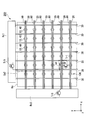
- FIG. 6 is a schematic diagram of the magnetic memory according to the second embodiment.
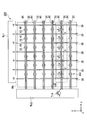
- FIG. 7 is a circuit diagram of the magnetic memory according to the second embodiment.
- the magnetic memory 200 has a memory region Rm and peripheral circuit regions Rc1 and Rc2.
- the memory region Rm has a plurality of element portions 10, a plurality of spin orbit torque wirings 20, a plurality of conductive portions 30, a plurality of gate portions 40, and a plurality of wirings 90.
- the same components as those of the spin orbit torque type magnetoresistive effect element 100 according to the first embodiment are designated by the same reference numerals, and the description thereof will be omitted.
- the memory region Rm of the magnetic memory 200 has a plurality of spin orbit torque type magnetoresistive effect elements 100.
- a portion including one element portion 10, the spin orbit torque wiring 20, the two conductive portions 30, and one gate portion 40 corresponds to the spin orbit torque type magnetoresistive effect element 100 according to the first embodiment.
- the plurality of spin orbit torque type magnetoresistive effect elements 100 are arranged in the x direction and the y direction.
- the plurality of spin orbit torque type magnetoresistive effect elements 100 arranged in the x direction will be referred to as a first element row L1
- the plurality of spin orbit torque type magnetoresistive effect elements 100 arranged in the y direction will be referred to as a second element row R1.
- FIG. 8 is a cross-sectional view of the spin orbit torque type magnetoresistive effect element 100 that constitutes the magnetic memory 200 according to the second embodiment.
- FIG. 8 is a cross-sectional view of two spin orbit torque type magnetoresistive effect elements 100 that are adjacent to the first element row L1 in the x direction.
- first element 100a one of the two spin orbit torque type magnetoresistive effect elements 100 is referred to as a first element 100a, and the other is referred to as a second element 100b.
- the second conductive portion 32 of the first element 100a functions as the first conductive portion 31 of the second element 100b. That is, the second conductive portion 32 of the first element 100a is shared as the first conductive portion 31 of the second element 100b.
- the spin orbit torque wiring 21 of the first element 100a and the spin orbit torque wiring 22 of the second element 100b are connected to each other to form one spin orbit torque wiring 20.
- the conductive portion 30 extends over the plurality of spin orbit torque wirings 20.
- the respective first conductive portions 31 of the plurality of spin orbit torque type magnetoresistive effect elements 100 constituting the second element row L2 are connected to each other to form one first conductive portion 31.
- the second conductive portions 32 of each of the plurality of spin orbit torque type magnetoresistive effect elements 100 forming the second element row L2 are connected to each other to form one second conductive portion 32.
- the peripheral circuit areas Rc1 and Rc2 are located outside the memory area Rm.
- the peripheral circuit region Rc1 has a fifth transistor Tr5.
- the fifth transistor Tr5 is connected to the conductive portion 30.
- the fifth transistor Tr5 controls the current flowing through the conductive portion 30.
- the peripheral circuit region Rc2 has a sixth transistor Tr6.
- the sixth transistor Tr6 is connected to the wiring 90.
- the sixth transistor Tr6 controls the current flowing through the wiring 90 and applies a voltage to the gate electrode 42 of the gate section 40.
- the fifth transistor Tr5 and the sixth transistor Tr6 are located outside the memory region Rm. Therefore, the fifth transistor Tr5 and the sixth transistor Tr6 have little influence on the integration of the magnetic memory 200.
- FIG. 9 is a circuit diagram for explaining a data write operation of the magnetic memory 200.
- a specific description will be given of a case where data is written to one spin orbit torque type magnetoresistive effect element (hereinafter, referred to as a selection element sd) among a plurality of spin orbit torque type magnetoresistive effect elements in the memory region Rm.
- a selection element sd spin orbit torque type magnetoresistive effect element
- the data write operation to the selection element sd is performed by the following procedure, for example. First, a part of the fifth transistor Tr5 in the peripheral circuit region Rc1 is turned on.
- the fifth transistor Tr5 to be turned on is the fifth transistor Tr5 connected to the two conductive parts 30 that sandwich the selection element sd closest thereto (in FIG. 9, only the fifth transistor Tr5 to be turned on is shown).
- the sixth transistor Tr6 to be turned on is the sixth transistor Tr6 connected to the wiring 90 connected to the selection element sd (in FIG. 9, only the sixth transistor Tr6 to be turned on is shown).
- a current flows through the wiring 90 a voltage is applied to the gate portion 40 and a channel is formed in a part of the spin orbit torque wiring 20.
- FIG. 10 is a circuit diagram for explaining a data read operation of the magnetic memory 200.
- a specific description will be given by taking as an example a case where data is read from one spin orbit torque type magnetoresistive effect element (hereinafter referred to as a selection element sd) among a plurality of spin orbit torque type magnetoresistive effect elements in the memory region Rm.
- a selection element sd spin orbit torque type magnetoresistive effect element
- the data read operation from the selection element sd is performed in the following procedure, for example. First, a part of the fifth transistor Tr5 in the peripheral circuit region Rc1 is turned on.
- the fifth transistor Tr5 that is turned on is the fifth transistor Tr5 that is connected to either one of the two conductive portions 30 that sandwich the selection element sd closest thereto (in FIG. 10, only the fifth transistor Tr5 that is turned on is selected). (Shown).
- the sixth transistor Tr6 to be turned on is the sixth transistor Tr6 connected to the wiring 90 connected to the selection element sd (in FIG. 9, only the sixth transistor Tr6 to be turned on is shown).
- a current flows through the wiring 90 a voltage is applied to the gate portion 40 and a channel is formed in a part of the spin orbit torque wiring 20.
- the first transistor Tr1 connected to the selection element sd is turned on (in FIG. 10, only the first transistor Tr1 to be turned on is shown).
- a current path Cp2 that connects the turned-on fifth transistor Tr5 and the turned-on first transistor Tr1 is formed. ..
- a resistance value of the selection element sd is read as data by causing a current to flow along the current path Cp2 and obtaining the potential difference between the current paths Cp2.
- the magnetic memory 200 can record multivalued information by using a plurality of spin orbit torque type magnetoresistive effect elements 100.
- spin orbit torque type magnetoresistive effect element 100 records binary data in a high resistance state and a low resistance state.
- Multi-valued information means information with three or more values.
- FIG. 11 is a circuit diagram for explaining another example of the data write operation of the magnetic memory 200.
- data is written at once to the same element row (hereinafter, referred to as selected element row sdL).
- the selection element row sdL turns on the sixth transistor Tr6 connected to the selection element row sdL in the peripheral circuit region Rc2 (in FIG. 11, only the sixth transistor Tr6 to be turned on is shown).
- the potential connected to each fifth transistor Tr5 is changed.
- the potential of the conductive portion 30 is a positive potential (denoted as +V in FIG. 11), a zero potential (denoted as G in FIG. 11), and a negative potential ( ⁇ V in FIG. 11). ,), zero potential, positive potential, zero potential, and positive potential.
- current flows in the +x direction, +x direction, ⁇ x direction, ⁇ x direction, +x direction, and ⁇ x direction between the two conductive parts 30 in order from the left.
- the magnetization of the first ferromagnetic layer 1 of the element unit 10 changes according to the direction of the current flowing in the spin orbit torque wiring 20. For example, when a current flows in the +x direction of the spin orbit torque wiring 20, the magnetization of the first ferromagnetic layer 1 becomes antiparallel to the magnetization of the second ferromagnetic layer 2. Further, for example, when a current flows in the ⁇ x direction of the spin orbit torque wiring 20, the magnetization of the first ferromagnetic layer 1 becomes parallel to the magnetization of the second ferromagnetic layer 2.
- the spin orbit torque type magnetoresistive effect element 100 records information of “1”, “1”, “0”, “0”, “1”, “0” in order from the left. ..
- the magnetic memory 200 records the sum of the information of two spin orbit torque type magnetoresistive effect elements 100 adjacent in the x direction as one information.
- the sum of the information of the two leftmost spin orbit torque type magnetoresistive effect elements 100 in the selection element array sdL is “2”.
- the sum of the information of the third and fourth spin-orbit torque type magnetoresistive effect elements 100 from the left in the selection element array sdL is “0”.
- the sum of the information of the fifth and sixth spin orbit torque type magnetoresistive effect elements 100 from the left of the selection element array sdL is “1”. That is, the magnetic memory 200 can record ternary information of “2”, “1”, and “0”.
- the magnetic memory 200 may record the difference between the information of two spin orbit torque type magnetoresistive effect elements 100 adjacent in the x direction as one information. For example, the difference in information between the two leftmost spin orbit torque type magnetoresistive effect elements 100 in the selection element array sdL is “0”. Further, for example, the difference in information between the third and fourth spin orbit torque type magnetoresistive effect elements 100 from the left of the selection element array sdL is “0”. Further, for example, the difference in information between the fifth and sixth spin orbit torque type magnetoresistive effect elements 100 from the left of the selection element array sdL is “1”.
- the spin orbit torque type magnetoresistive effect element 100 is integrated with high density. Further, since the two spin orbit torque type magnetoresistive effect elements 100 belonging to the first element row L1 share the conductive portions 30, the number of the conductive portions 30 can be reduced and the integration property of the magnetic memory 200 can be further enhanced. You can
- the plurality of spin orbit torque type magnetoresistive effect elements 100 belonging to the first element row L1 share the spin orbit torque wiring 20, and the plurality of spin orbit torque type magnetoresistive effect elements 100 belonging to the second element row R1 are conductive portions.
- the number of wirings forming the magnetic memory 200 is reduced. The reduction in the number of wirings improves the integration of the magnetic memory 200. Further, the reduction in the number of wirings facilitates the manufacture of the magnetic memory 200.
- the magnetic memory 200 can record multivalued information depending on the data recording method.
- FIG. 12 is a circuit of a third modification of the magnetic memory according to the second embodiment.
- the same components as those of the magnetic memory 200 according to the second embodiment are designated by the same reference numerals and the description thereof will be omitted.
- the spin-orbit torque wirings 20 in the first element row L1 are not connected to each other, and the first spin-torque torque magnetoresistive effect element 100 is provided between two adjacent spin-orbit torque magnetoresistive effect elements 100. It differs from the magnetic memory 200 shown in FIG. 7 in that the conductive portion 31 and the second conductive portion 32 are not used.
- the number of transistors in the memory region Rm is small, and the spin-orbit torque type magnetoresistive effect element 100 has high integration.
Landscapes
- Hall/Mr Elements (AREA)
- Mram Or Spin Memory Techniques (AREA)
Abstract
本実施形態にかかるスピン軌道トルク型磁気抵抗効果素子は、第1強磁性層と、第2強磁性層と、前記第1強磁性層と前記第2強磁性層との間に位置する非磁性層と、を有する素子部と、前記素子部に対し第1方向に位置し、前記素子部の前記第1強磁性層に面し、第2方向に延びるスピン軌道トルク配線と、前記第1方向から見て前記素子部を挟む位置で、前記スピン軌道トルク配線に面する第1導電部及び第2導電部と、前記第1方向から見て前記第1導電部と前記第2導電部との間に位置し、前記スピン軌道トルク配線の前記素子部に面する第1面と反対側の第2面に面し、前記スピン軌道トルク配線に近い位置から順にゲート絶縁層とゲート電極とを有するゲート部と、を備え、前記スピン軌道トルク配線は、散乱元素が添加された半導体を含む。
Description
本発明は、スピン軌道トルク型磁気抵抗効果素子及び磁気メモリに関するものである。
磁気抵抗効果素子は、磁気センサ、高周波部品、磁気ヘッド及び不揮発性ランダムアクセスメモリ(MRAM)への応用が期待されている。
磁気抵抗効果素子は、非磁性層を挟む二つの強磁性層の互いの磁化の向きの変化を素子の抵抗変化として出力する。磁気抵抗効果素子は、強磁性層の磁化の向きを制御して、データを記録する。磁化の向きを制御する方法として、電流が生み出す磁場を利用する方式、磁気抵抗効果素子の積層方向に電流を流した際に生ずるスピントランスファートルク(STT)を利用する方式が知られている。STTを利用する方式は、非磁性層を貫通する方向に電位差を与える必要があり、非磁性層にダメージを与える場合がある。
近年、磁化の向きを制御する新たな方式としてスピン軌道トルク(SOT)を利用する方式が検討されている(例えば、特許文献1)。SOTは、スピン軌道相互作用によって生じたスピン流又は異種材料の界面におけるラシュバ効果により強磁性層内に誘起される。SOTは、強磁性層内の磁化に作用し、強磁性層の磁化を反転する。スピン流及びラシュバ効果は、強磁性層の積層方向と交差する方向に電流が流れると生じる。SOTを利用する方式は、非磁性層及び強磁性層の積層方向に大きな書き込み電流を流すことを避けられ、非磁性層等へのダメージを抑制できる。
磁気抵抗効果素子は、データを記録する記録領域であり、複数の磁気抵抗効果素子を集積した磁気メモリとして用いることが多い。磁気メモリ全体の小型化を図るためには、磁気抵抗効果素子の集積性を高めることが求められている。
本発明は上記事情に鑑みてなされたものであり、集積性を高めることができるスピン軌道トルク型磁気抵抗効果素子を提供することを目的とする。また集積性の高い磁気メモを提供することを目的とする。
本発明は、上記課題を解決するため、以下の手段を提供する。
(1)第1の態様にかかるスピン軌道トルク型磁気抵抗効果素子は、第1強磁性層と、第2強磁性層と、前記第1強磁性層と前記第2強磁性層との間に位置する非磁性層と、を有する素子部と、前記素子部に対し第1方向に位置し、前記素子部の前記第1強磁性層に面し、第2方向に延びるスピン軌道トルク配線と、前記第1方向から見て前記素子部を挟む位置で、前記スピン軌道トルク配線に面する第1導電部及び第2導電部と、前記第1方向から見て前記第1導電部と前記第2導電部との間に位置し、前記スピン軌道トルク配線の前記素子部に面する第1面と反対側の第2面に面し、前記スピン軌道トルク配線に近い位置から順にゲート絶縁層とゲート電極とを有するゲート部と、を備え、前記スピン軌道トルク配線は、半導体を含む。
(2)上記態様にかかるスピン軌道トルク型磁気抵抗効果素子は、前記素子部の第2強磁性層に接続され、前記第1方向に延びるビア配線と、前記ビア配線により前記素子部と電気的に接続された第1トランジスタと、を備えてもよい。
(3)上記態様にかかるスピン軌道トルク型磁気抵抗効果素子において、前記スピン軌道トルク配線を構成する半導体は、Si、SiGe、GaAs、Ge、InGaAsからなる群から選択されるいずれかであってもよい。
(4)上記態様にかかるスピン軌道トルク型磁気抵抗効果素子において、前記スピン軌道トルク配線は散乱元素を含んでもよい。
(5)上記態様にかかるスピン軌道トルク型磁気抵抗効果素子において、前記散乱元素は、イットリウム以上の原子番号を有する重金属元素であってもよい。
(6)上記態様にかかるスピン軌道トルク型磁気抵抗効果素子において、前記散乱元素は、磁性元素であってもよい。
(7)第2の態様にかかる磁気メモリは、上記態様にかかるスピン軌道トルク型磁気抵抗効果素子を複数備える。
(8)上記態様にかかる磁気メモリにおいて、複数の前記スピン軌道トルク型磁気抵抗効果素子は、前記スピン軌道トルク型磁気抵抗効果素子が前記第2方向に配列した第1素子列を有し、前記第1素子列において、前記第2方向に隣接する2つの前記スピン軌道トルク型磁気抵抗効果素子は、一方の前記スピン軌道トルク型磁気抵抗効果素子の前記第2導電部を、他方の前記スピン軌道トルク型磁気抵抗効果素子の前記第1導電部として共有している。
(9)上記態様にかかる磁気メモリにおいて、複数の前記スピン軌道トルク型磁気抵抗効果素子は、前記スピン軌道トルク型磁気抵抗効果素子が前記第2方向に配列した第1素子列を有し、前記第1素子列を構成する複数の前記スピン軌道トルク型磁気抵抗効果素子のそれぞれのスピン軌道トルク配線は、互いに接続されていてもよい。
(10)上記態様にかかる磁気メモリにおいて、複数の前記スピン軌道トルク型磁気抵抗効果素子は、前記スピン軌道トルク型磁気抵抗効果素子が前記第1方向及び前記第2方向と異なる第3方向に配列した第2素子列をさらに有し、前記第2素子列を構成する複数の前記スピン軌道トルク型磁気抵抗効果素子のそれぞれの第1導電部は互いに接続され、前記第2素子列を構成する複数の前記スピン軌道トルク型磁気抵抗効果素子のそれぞれの第2導電部は互いに接続されていてもよい。
上記態様にかかるスピン軌道トルク型磁気抵抗効果素子によれば、素子の集積性を高めることができる。また上記態様にかかる磁気メモリは小型化が可能である。
以下、本実施形態について、図を適宜参照しながら詳細に説明する。以下の説明で用いる図面は、特徴をわかりやすくするために便宜上特徴となる部分を拡大して示している場合があり、各構成要素の寸法比率などは実際とは異なっていることがある。以下の説明において例示される材料、寸法等は一例であって、本発明はそれらに限定されるものではなく、本発明の効果を奏する範囲で適宜変更して実施することが可能である。
まず方向について定義する。z方向は、後述する素子部10に対しスピン軌道トルク配線20が位置する方向である。x方向は、後述するスピン軌道トルク配線が延びる方向である。y方向は、x方向及びz方向と直交する方向である。z方向は第1方向の一例であり、x方向は第2方向の一例であり、y方向は第3方向の一例である。また本明細書で「x方向に延びる」とは、例えば、x方向、y方向、及びz方向の各寸法のうち最小の寸法よりもx方向の寸法が大きいことを意味する。他の方向に延びる場合も同様である。
「第1実施形態」
(スピン軌道トルク型磁気抵抗効果素子)
図1は、第1実施形態にかかるスピン軌道トルク型磁気抵抗効果素子の要部の断面図である。図2は、第1実施形態にかかるスピン軌道トルク型磁気抵抗効果素子の断面図である。図1及び図2は、後述するスピン軌道トルク配線20のy方向の中央を通るxz平面で切断した断面である。
(スピン軌道トルク型磁気抵抗効果素子)
図1は、第1実施形態にかかるスピン軌道トルク型磁気抵抗効果素子の要部の断面図である。図2は、第1実施形態にかかるスピン軌道トルク型磁気抵抗効果素子の断面図である。図1及び図2は、後述するスピン軌道トルク配線20のy方向の中央を通るxz平面で切断した断面である。
スピン軌道トルク型磁気抵抗効果素子100は、素子部10と、スピン軌道トルク配線20と、複数の導電部30と、ゲート部40と、複数のビア配線50と、基板60と、絶縁層80と、読み出し配線Rpと、を備える。
<素子部>
素子部10は、第1強磁性層1と第2強磁性層2と非磁性層3とを有する。素子部10は、スピン軌道トルク配線20の第1面20aに面する。ここで「面する」とは、互いに向き合う関係を言い、2つの層が接触していても、間に他の層を有してもよい。素子部10は、第1強磁性層1の磁化と第2強磁性層2の磁化との相対角の違いに基づき、z方向の抵抗値が変化する磁気抵抗効果素子である。
素子部10は、第1強磁性層1と第2強磁性層2と非磁性層3とを有する。素子部10は、スピン軌道トルク配線20の第1面20aに面する。ここで「面する」とは、互いに向き合う関係を言い、2つの層が接触していても、間に他の層を有してもよい。素子部10は、第1強磁性層1の磁化と第2強磁性層2の磁化との相対角の違いに基づき、z方向の抵抗値が変化する磁気抵抗効果素子である。
素子部10は、例えば、柱状体である。z方向から見た際の素子部10の形状は、特に問わない。素子部10は、z方向から見て、例えば、円形、四角形、楕円形である。素子部10のx方向及びy方向の幅は、z方向に一定でも、変化してもよい。例えば、素子部10のx方向及びy方向の幅は、スピン軌道トルク配線20から離れるに従い、大きくなってもよく、小さくなってもよい。
第1強磁性層1は、強磁性体、特に軟磁性体を含む。第1強磁性層1は、磁化自由層と言われる場合がある。第1強磁性層1は、例えば、Cr、Mn、Co、Fe及びNiからなる群から選択される金属、これらの金属を1種以上含む合金、これらの金属とB、C、及びNの少なくとも1種以上の元素とが含まれる合金を含む。第1強磁性層1は、例えば、Co-Fe、Co-Fe-B、Ni-Fe、Co-Ho合金、Sm-Fe合金、Fe-Pt合金、Co-Pt合金、CoCrPt合金である。
第1強磁性層1は、Co2FeSi等のホイスラー合金を含んでもよい。ホイスラー合金は、XYZまたはX2YZの化学組成をもつ金属間化合物を含む。Xは周期表上でCo、Fe、Ni、あるいはCu族の遷移金属元素または貴金属元素であり、YはMn、V、CrあるいはTi族の遷移金属又はXの元素種であり、ZはIII族からV族の典型元素である。ホイスラー合金は、例えば、Co2FeSi、Co2FeGe、Co2FeGa、Co2MnSi、Co2Mn1-aFeaAlbSi1-b、Co2FeGe1-cGac等である。ホイスラー合金は高いスピン分極率を有する。
第1強磁性層1は、xy面内のいずれかの方向又はz方向に磁化容易軸を有する。第1強磁性層1がxy面内のいずれかの方向に磁化容易軸を有する場合、第1強磁性層1は面内磁化膜と言われる。第1強磁性層1がz方向に磁化容易軸を有する場合、第1強磁性層1は垂直磁化膜と言われる。
第2強磁性層2は、第1強磁性層1と非磁性層3を挟む位置にある。第2強磁性層2は、強磁性体を含む。第2強磁性層2を構成する強磁性体は、例えば、第1強磁性層1と同様の材料が用いられる。
第2強磁性層2の磁化は、第1強磁性層1の磁化より所定の環境下で動きにくい。第2強磁性層2は、磁化固定層と言われる場合がある。
第2強磁性層2は、例えば、第2強磁性層2は、一つの強磁性体からなる。この場合、第2強磁性層2を構成する材料は、第1強磁性層1より保磁力が高くなるものを選択する。
また例えば、第2強磁性層2は、第1層と第2層と第3層とを有する。第1層と第2層とは、強磁性体からなり、互いに反強磁性結合する。第3層は、第1層と第2層との間に挟まれた非磁体である。第1層と第2層は、第1強磁性層1と同様の材料からなる。第3層は、例えば、Ru等からなる。第1層と第2層とが反強磁性結合することで、第2強磁性層2全体の保磁力が第1強磁性層1の保磁力より大きくなる。
非磁性層3は、第1強磁性層1と第2強磁性層2との間に位置する。
非磁性層3は、非磁性の絶縁体、半導体又は金属からなる。非磁性層3が絶縁体からなる場合、素子部10はトンネル磁気効果(TMR)素子である。非磁性層3が半導体又は金属からなる場合、素子部10は巨大磁気抵抗効果(GMR)素子である。
非磁性の絶縁体は、例えば、Al2O3、SiO2、MgO、MgAl2O4、およびこれらのAl、Ga、Si、Mgの一部がZn、Be等に置換された材料である。非磁性層3が非磁性の絶縁体からなる場合、非磁性層3はトンネルバリア層である。MgOやMgAl2O4は、第1強磁性層1と第2強磁性層2との間にコヒーレントトンネルを実現しやすい。非磁性の金属は、例えば、Cu、Au、Ag等である。さらに、非磁性の半導体は、例えば、Si、Ge、Si-Ge、CuInSe2、CuGaSe2、Cu(In,Ga)Se2等である。
素子部10は、第1強磁性層1、第2強磁性層2及び非磁性層3以外の層を有してもよい。
<スピン軌道トルク配線>
スピン軌道トルク配線20は、素子部10のz方向に位置する。スピン軌道トルク配線20は、素子部10の第1強磁性層1に面する。スピン軌道トルク配線20は、z方向から見て、2つの導電部30に亘ってx方向に延びる。
スピン軌道トルク配線20は、素子部10のz方向に位置する。スピン軌道トルク配線20は、素子部10の第1強磁性層1に面する。スピン軌道トルク配線20は、z方向から見て、2つの導電部30に亘ってx方向に延びる。
スピン軌道トルク配線20の両端に電位差を与えると、スピン軌道トルク配線20に沿って電流Iが流れる。一方向に配向した第1スピンs1と、第1スピンs1と反対方向に配向した第2スピンs2とは、それぞれ電流と直交する方向に曲げられる。例えば、+y方向に配向した第1スピンs1が+z方向に曲げられ、-y方向に配向した第2スピンs2が-z方向に曲げられる。
通常のホール効果とスピンホール効果とは、運動(移動)する電荷(電子)が運動(移動)方向を曲げられる点で共通する。一方で、通常のホール効果は磁場中で運動する荷電粒子がローレンツ力を受けて運動方向を曲げられるのに対して、スピンホール効果は磁場が存在しなくても、電子が移動するだけ(電流が流れるだけ)でスピンの移動方向が曲げられる点が大きく異なる。
非磁性体(強磁性体ではない材料)は、スピンホール効果により生じる第1スピンs1の電子数と第2スピンs2の電子数とが等しい。図1において、+z方向に向かう第1スピンs1の電子数と-z方向に向かう第2スピンs2の電子数とは等しい。この場合、電荷の流れは互いに相殺され、電流量はゼロとなる。電流を伴わないスピン流は特に純スピン流と呼ばれる。
第1スピンs1の電子の流れをJ↑、第2スピンs2の電子の流れをJ↓、スピン流をJSと表すと、JS=J↑-J↓で定義される。スピン流JSは、z方向に生じる。図1において、スピン軌道トルク配線20は素子部10に面する。スピンは、スピン軌道トルク配線20から素子部10の第1強磁性層1に注入される。注入されたスピンは、スピン軌道トルク(SOT)を、第1強磁性層1の磁化にくわえる。第1強磁性層1の磁化は、スピン軌道トルク(SOT)により磁化反転する。
スピン軌道トルク配線20は、半導体を含む。スピン軌道トルク配線20を構成する半導体は、例えば、Si、SiGe、GaAs、Ge、InGaAsからなる群から選択されるいずれかである。スピン軌道トルク配線20は、散乱元素が添加された半導体でも良い。散乱元素は、例えば、イットリウム(Y)以上の原子番号を有する重金属元素である。散乱元素は、また例えば、磁性元素である。
半導体は、例えば、非磁性の重金属と比較して、スピン軌道相互作用が小さい。スピン軌道トルク配線20に半導体を用いた場合、スピン流の生成効率は低いが、スピン軌道トルク配線20に大きな電流密度の電流を印加すれば、第1強磁性層1の磁化を反転させるのに十分なトルクを第1強磁性層1の磁化に与えることができる。また半導体に散乱元素を添加すると、散乱元素がスピンの散乱因子となる。スピン軌道トルク配線20内部を移動するスピンが散乱するとスピン軌道相互作用が増強され、スピン軌道トルク配線20に印加した電流の電流密度に対するスピン流の生成効率が向上する。その結果、スピン軌道トルク配線20に散乱元素が添加された半導体を用いた場合は、スピン軌道トルク配線20に印加する電流量を大幅に低減できる。スピン軌道トルク配線20に散乱元素が添加された半導体を用いた場合は、スピン軌道トルク配線20が非磁性の重金属の場合と同等の電流密度の電流を印加すれば、第1強磁性層1の磁化を反転させるのに十分なトルクを第1強磁性層1の磁化に与えることができる。
散乱元素の添加量は、例えば、1×1013cm-3以上1×1018cm-3以下である。散乱元素が増大し過ぎると、スピン軌道トルク配線20が金属的な挙動を示す。また散乱元素が増大すると、発生したスピン流のz方向の移動が、散乱元素によって阻害され、スピン流の生成効率が低下する場合がある。
<導電部>
導電部30は、z方向から見て、素子部10を挟む位置に設けられている。図1に示す導電部30は、スピン軌道トルク配線20の第2面20bに面する。第2面20bは、素子部10に面する第1面20aと反対側の面である。導電部30は、第1面20aに面してもよい。以下、便宜上、2つの導電部30のうちの一方を第1導電部31と称し、他方を第2導電部32と称する。
導電部30は、z方向から見て、素子部10を挟む位置に設けられている。図1に示す導電部30は、スピン軌道トルク配線20の第2面20bに面する。第2面20bは、素子部10に面する第1面20aと反対側の面である。導電部30は、第1面20aに面してもよい。以下、便宜上、2つの導電部30のうちの一方を第1導電部31と称し、他方を第2導電部32と称する。
導電部30は、例えば、配線、電極である。導電部30は、導電性を有する材料からなる。導電部30は、例えば、アルミニウム、銅、銀である。導電部30が配線の場合、図1に示す導電部30はy方向に延びる。
<ゲート部>
ゲート部40は、z方向から見て、第1導電部31と第2導電部32との間に位置する。ゲート部40は、スピン軌道トルク配線20の第2面20bに面する。ゲート部40は、例えば、スピン軌道トルク配線20を挟んで、素子部10と対向する。
ゲート部40は、z方向から見て、第1導電部31と第2導電部32との間に位置する。ゲート部40は、スピン軌道トルク配線20の第2面20bに面する。ゲート部40は、例えば、スピン軌道トルク配線20を挟んで、素子部10と対向する。
ゲート部40は、スピン軌道トルク配線20に近い位置から、ゲート絶縁層41とゲート電極42とを有する。ゲート絶縁層41は、例えば、酸化シリコン(SiOx)、窒化シリコン(SiNx)、炭化シリコン(SiC)、窒化クロム、炭窒化シリコン(SiCN)、酸窒化シリコン(SiON)、酸化アルミニウム(Al2O3)、酸化ジルコニウム(ZrOx)である。ゲート電極42は、導電性を有する材料からなる。ゲート電極42は、例えば、アルミニウム、銅、銀である。
ゲート部40のx方向の幅は、例えば、素子部10のx方向の幅より広い。ゲート電極42に電圧を印加すると、第1導電部31と第2導電部32との間にチャネルが形成され、第1導電部31と第2導電部32とが導通する。ゲート部40のx方向の幅が広いと、第1導電部31と第2導電部32との間の漏れ電流が抑制される。
<ビア配線>
ビア配線50は、第1絶縁層81及び第2絶縁層82内に位置する(図2参照)。ビア配線50は、第1絶縁層81及び第2絶縁層82に設けられた開口内に形成される。ビア配線50は、例えば、z方向に延びる。ビア配線50は、複数ある。以下、便宜上、素子部10の第2強磁性層2と基板60とを電気的に接続するビア配線50を第1ビア配線51と称し、読み出し配線Rpと基板60とを電気的に接続するビア配線50を第2ビア配線52と称する。
ビア配線50は、第1絶縁層81及び第2絶縁層82内に位置する(図2参照)。ビア配線50は、第1絶縁層81及び第2絶縁層82に設けられた開口内に形成される。ビア配線50は、例えば、z方向に延びる。ビア配線50は、複数ある。以下、便宜上、素子部10の第2強磁性層2と基板60とを電気的に接続するビア配線50を第1ビア配線51と称し、読み出し配線Rpと基板60とを電気的に接続するビア配線50を第2ビア配線52と称する。
ビア配線50は、導電性の高い材料を含む。ビア配線50は、例えば、銅、アルミニウム、銀、導電性を有する酸化膜、導電性を有する窒化膜、アモルファスシリコン等である。
<基板>
基板60は、例えば、半導体基板である。基板60は、例えば、シリコン基板である。基板60は、ソース領域S1及びドレイン領域D1を有する。ソース領域S1及びドレイン領域D1は、基板60に不純物が注入された領域である。
基板60は、例えば、半導体基板である。基板60は、例えば、シリコン基板である。基板60は、ソース領域S1及びドレイン領域D1を有する。ソース領域S1及びドレイン領域D1は、基板60に不純物が注入された領域である。
基板60の表面近傍には、第1トランジスタTr1が形成される。第1トランジスタTr1は、ソース領域S1、ドレイン領域D1、ゲート電極G1、ゲート絶縁層GI1を有する。第1トランジスタTr1は、第1ビア配線51により素子部10と電気的に接続される。
ゲート電極G1及びゲート絶縁層GI1は、z方向から見て、ソース領域S1とドレイン領域D1との間に位置する。ゲート電極G1は、基板60の表面に面する。ゲート絶縁層GI1は、基板60とゲート電極G1との間に位置する。ゲート電極G1は、ゲート電極42と同様の材料からなり、ゲート絶縁層GI1は、ゲート絶縁層41と同様の材料からなる。
<絶縁層>
絶縁層80は、多層配線の配線間や素子間を絶縁する絶縁層である。絶縁層80は、ビア配線50を除き、素子部10と第1トランジスタTr1と読み出し配線Rpとを絶縁する。絶縁層80は、例えば、第1絶縁層81と第2絶縁層82と第3絶縁層83と第4絶縁層84を有する。第1絶縁層81は、基板60と読み出し配線Rpとの間に位置する。第2絶縁層82は、読み出し配線Rpより素子部10に近い位置で、第1ビア配線51の周囲を覆う。第3絶縁層83は、素子部10の周囲を覆う。第4絶縁層84は、スピン軌道トルク配線20の周囲を覆う。
絶縁層80は、多層配線の配線間や素子間を絶縁する絶縁層である。絶縁層80は、ビア配線50を除き、素子部10と第1トランジスタTr1と読み出し配線Rpとを絶縁する。絶縁層80は、例えば、第1絶縁層81と第2絶縁層82と第3絶縁層83と第4絶縁層84を有する。第1絶縁層81は、基板60と読み出し配線Rpとの間に位置する。第2絶縁層82は、読み出し配線Rpより素子部10に近い位置で、第1ビア配線51の周囲を覆う。第3絶縁層83は、素子部10の周囲を覆う。第4絶縁層84は、スピン軌道トルク配線20の周囲を覆う。
絶縁層80は、例えば、半導体デバイス等の層間絶縁層に用いられる材料と同様の材料からなる。絶縁層80は、例えば、酸化シリコン(SiOx)、窒化シリコン(SiNx)、炭化シリコン(SiC)、窒化クロム、炭窒化シリコン(SiCN)、酸窒化シリコン(SiON)、酸化アルミニウム(Al2O3)、酸化ジルコニウム(ZrOx)等である。
次いで、第1実施形態にかかるスピン軌道トルク型磁気抵抗効果素子100の動作について説明する。
スピン軌道トルク型磁気抵抗効果素子100は、第1強磁性層1の磁化の向きを制御して、データを書き込む。またスピン軌道トルク型磁気抵抗効果素子100は、第1強磁性層1の磁化と第2強磁性層2の磁化との相対角の違いに伴う素子部10の抵抗値の変化を、データとして読み出す。
まずスピン軌道トルク型磁気抵抗効果素子100へのデータの書き込みについて説明する。スピン軌道トルク型磁気抵抗効果素子100へデータを書き込む場合、まずゲート電極42に電圧を印加する。スピン軌道トルク配線20は半導体であるため、ゲート電極42に電圧を印加すると、第1導電部31と第2導電部32との間にチャネルが形成される。チャネルは、電子の通路である。第1導電部31と第2導電部32との間にチャネルが形成されると、スピン軌道トルク配線20に電流Iが流れる。
スピン軌道トルク配線20に電流Iが流れると、スピンホール効果により第1スピンs1と第2スピンs2とがスピン軌道トルク配線20の表面近傍に偏在する。スピン軌道トルク配線20の内部では、第1スピンs1及び第2スピンs2の偏在を解消する方向(z方向)にスピン流が生成される。スピン軌道トルク配線20内のスピンの一部は、スピン流により素子部10の第1強磁性層1に注入される。
第1強磁性層1に注入されたスピンは、第1強磁性層1の磁化にスピン軌道トルク(SOT)を与える。第1強磁性層1の磁化は、スピン軌道トルクを受けて、回転(反転)する。第1強磁性層1の磁化の向きが変わることで、素子部10の抵抗値が変動し、スピン軌道トルク型磁気抵抗効果素子100にデータが書き込まれる。
次いで、スピン軌道トルク型磁気抵抗効果素子100からのデータの読み出しについて説明する。まず第1トランジスタTr1のゲート電極G1及びゲート部40のゲート電極42に電圧を印加する。ゲート電極G1に電圧を印加すると、ソース領域S1とドレイン領域D1とが導通する。またゲート電極42に電圧を印加すると、第1導電部31又は第2導電部32と素子部10との間が導通する。これらの間が導通すると、読み出し配線Rpと第1導電部31又は第2導電部32との間に電流の経路が形成される。読み出し配線Rpと第1導電部31又は第2導電部32との間の電位差を測定し、スピン軌道トルク型磁気抵抗効果素子100の抵抗値が求められる。スピン軌道トルク型磁気抵抗効果素子100の抵抗値は、素子部10の第1強磁性層1と第2強磁性層2との磁化の相対角の違いにより変化する。したがって、スピン軌道トルク型磁気抵抗効果素子100の抵抗値からデータを読み出すことができる。
次いで、第1実施形態にかかるスピン軌道トルク型磁気抵抗効果素子100の製造方法について、図2を基に説明する。
まず基板60にソース領域S1,ドレイン領域D1を形成する。ソース領域S1及びドレイン領域D1は公知の方法で形成される。ソース領域S1とドレイン領域D1との間には、ゲート絶縁層GI1及びゲート電極G1が形成される。
次いで、基板60、ゲート絶縁層GI1及びゲート電極G1を覆うように第1絶縁層81が形成される。第1絶縁層81には、第1絶縁層81の表面からドレイン領域D1に向かう開口が形成される。開口は導体で充填され、第2ビア配線52が形成される。第2ビア配線52及び第1絶縁層81の一面は、化学機械研磨(CMP)で平坦化することが好ましい。
次いで、第2ビア配線52及び第1絶縁層81の一面に、読み出し配線Rp及び第2絶縁層82が形成される。第1絶縁層81、読み出し配線Rp及び第2絶縁層82には、第2絶縁層82の表面からソース領域S1に向かう開口が形成される。開口は導体で充填され、第1ビア配線51が形成される。第1ビア配線51及び第2絶縁層82の一面は、化学機械研磨(CMP)で平坦化することが好ましい。
次いで、z方向から見て、第1ビア配線51と重なる位置に素子部10が形成される。素子部10は各層を形成した後に、フォトリソグラフィー等により所定の形状に加工される。そして、素子部10の周囲に第3絶縁層83が形成される。
次いで、z方向から見て、素子部10と重なる位置にスピン軌道トルク配線20が形成される。スピン軌道トルク配線20は、フォトリソグラフィー等により所定の形状に加工される。そして、スピン軌道トルク配線20の周囲に第4絶縁層84が形成される。
次いで、スピン軌道トルク配線20の一面において、z方向から見て、素子部10と重なる位置にゲート部40が形成される。また最後に、スピン軌道トルク配線20の両端に、導電部30が形成される。このような手順で、第1実施形態にかかるスピン軌道トルク型磁気抵抗効果素子100が得られる。各層は、例えば、スパッタリング法、化学気相成長(CVD)法等により形成される。
第1実施形態にかかるスピン軌道トルク型磁気抵抗効果素子100によれば、複数の素子を集積する際の集積性を高めることができる。
図3は、ゲート部40を有さないスピン軌道トルク型磁気抵抗効果素子100Aの断面図である。スピン軌道トルク型磁気抵抗効果素子100Aは、ゲート部40を有さない点、基板61が複数のトランジスタを有する点、書き込み配線Wp及び共通配線Cmを有する点、第2絶縁層82が書き込み配線Wpにより第1部分82aと第2部分82bに分離されている点、及び、第3ビア配線53、第4ビア配線54、第5ビア配線55及び第6ビア配線56を有する点が、図2に示す第1実施形態にかかるスピン軌道トルク型磁気抵抗効果素子100と異なる。第1実施形態にかかるスピン軌道トルク型磁気抵抗効果素子100と同様の構成については、説明を省く。
基板61は、複数のソース領域S1,S2,S3及び複数のドレイン領域D1,D2,D3を有する。複数のソース領域S1,S2,S3及び複数のドレイン領域D1,D2,D3は、基板61に不純物が注入された領域である。基板61の表面近傍には、第1トランジスタTr1、第2トランジスタTr2及び第3トランジスタTr3が形成されている。第2トランジスタTr2は、ソース領域S2、ドレイン領域D2、ゲート電極G2、ゲート絶縁層GI2を有する。第3トランジスタTr3は、ソース領域S3、ドレイン領域D3、ゲート電極G3、ゲート絶縁層GI3を有する。
第3ビア配線53は、書き込み配線Wpとソース領域S2とを電気的に接続する。第4ビア配線54は、ドレイン領域D2と第1導電部31とを電気的に接続する。第5ビア配線55は、第2導電部32とソース領域S3とを電気的に接続する。第6ビア配線56は、ドレイン領域D3と共通配線Cmとを電気的に接続する。
例えば、スピン軌道トルク配線20が金属の場合、第1導電部31と第2導電部32との間は常に導通するため、ゲート部40によって第1導電部31と第2導電部32との間の通電を制御することはできない。したがって、図3に示すスピン軌道トルク型磁気抵抗効果素子100Aは、3つのトランジスタ(第1トランジスタTr1、第2トランジスタTr2及び第3トランジスタTr3)を用いて、データの書き込み及び読み出しを制御する。
素子部10がxy面内で占める面積と比較して、一つのトランジスタがxy面内で占める面積は大きい。図3に示すスピン軌道トルク型磁気抵抗効果素子100Aは、データの書き込み及び読み出しの制御のために、3つのトランジスタが必要である。したがって、図3に示すスピン軌道トルク型磁気抵抗効果素子100Aは、3つのトランジスタ分の面積が必要である。
これに対し、図2に示す第1実施形態にかかるスピン軌道トルク型磁気抵抗効果素子100は、データの書き込み及び読み出しの制御のために、1つのトランジスタ(第1トランジスタTr1)で足りる。したがって、図2に示すスピン軌道トルク型磁気抵抗効果素子100は、1つのトランジスタ分の面積で、動作することが可能であり、集積性に優れる。
以上、第1実施形態にかかるスピン軌道トルク型磁気抵抗効果素子100の一例について詳述したが、本発明の趣旨から逸脱しない範囲内で、構成の付加、省略、置換、及びその他の変更が可能である。
(第1変形例)
図4は、第1実施形態にかかるスピン軌道トルク型磁気抵抗効果素子の第1変形例の要部の断面図である。第1実施形態にかかるスピン軌道トルク型磁気抵抗効果素子100と同様の構成については、同様の符号を付し、説明を省く。
図4は、第1実施形態にかかるスピン軌道トルク型磁気抵抗効果素子の第1変形例の要部の断面図である。第1実施形態にかかるスピン軌道トルク型磁気抵抗効果素子100と同様の構成については、同様の符号を付し、説明を省く。
図4に示すゲート絶縁層41Aは、z方向から見て、ゲート電極42より広い面積を占める。ゲート絶縁層41は、スピン軌道トルク配線20の第2面20b及び第1導電部31及び第2導電部32の表面の一部を覆う。ゲート絶縁層41Aが第1導電部31及び第2導電部32にかかることで、第1導電部31又は第2導電部32とゲート電極42との絶縁性を高めることができる。
(第2変形例)
図5は、第1実施形態にかかるスピン軌道トルク型磁気抵抗効果素子の第2変形例の断面図である。第1実施形態にかかるスピン軌道トルク型磁気抵抗効果素子100と同様の構成については、同様の符号を付し、説明を省く。
図5は、第1実施形態にかかるスピン軌道トルク型磁気抵抗効果素子の第2変形例の断面図である。第1実施形態にかかるスピン軌道トルク型磁気抵抗効果素子100と同様の構成については、同様の符号を付し、説明を省く。
図5に示すスピン軌道トルク型磁気抵抗効果素子102は、素子部10より基板60側の構成が異なる。スピン軌道トルク型磁気抵抗効果素子102は、素子部10と、スピン軌道トルク配線20と、複数の導電部30と、ゲート部40と、第1ビア配線51と、絶縁膜57と、基板60と、複数の絶縁層80と、読み出し配線Rpと、ゲート配線Gpとを備える。
第1ビア配線51及び絶縁膜57と、ゲート配線Gpとの交差部分が、第4トランジスタTr4として機能する。絶縁膜57は、第1ビア配線51の周囲を被覆する。絶縁膜57は、例えば、酸化シリコンである。ゲート配線Gpは、例えば、導電性を有する材料からなる。第1ビア配線51は半導体であり、例えば、アモルファスシリコンである。
スピン軌道トルク型磁気抵抗効果素子102へデータを書き込む際は、第1実施形態にかかるスピン軌道トルク型磁気抵抗効果素子100と同様に行う。
スピン軌道トルク型磁気抵抗効果素子102からデータを読み出す際は、ゲート配線Gp及びゲート部40のゲート電極42に電圧を印加する。ゲート配線Gpに電圧を印加すると、読み出し配線Rpと素子部10との間が通電する。ゲート電極42に電圧を印加すると、素子部10と第1導電部31又は第2導電部32との間が通電する。これらの間が導通すると、読み出し配線Rpと第1導電部31又は第2導電部32との間に電流の経路が形成される。読み出し配線Rpと第1導電部31又は第2導電部32との間の電位差を測定し、スピン軌道トルク型磁気抵抗効果素子102の抵抗値が求められる。スピン軌道トルク型磁気抵抗効果素子102の抵抗値は、素子部10の第1強磁性層1と第2強磁性層2との磁化の相対角の違いにより変化する。したがって、スピン軌道トルク型磁気抵抗効果素子102の抵抗値からデータを読み出すことができる。
変形例2にかかるスピン軌道トルク型磁気抵抗効果素子102も、一つのトランジスタ(第4トランジスタTr4)で制御できるため、集積性に優れる。また第4トランジスタTr4は、素子部10とz方向に重なる位置に形成されているため、スピン軌道トルク型磁気抵抗効果素子102をより高密度に集積できる。
「第2実施形態」
(磁気メモリ)
図6は、第2実施形態にかかる磁気メモリの模式図である。図7は、第2実施形態にかかる磁気メモリの回路図である。磁気メモリ200は、メモリ領域Rmと周辺回路領域Rc1、Rc2を有する。メモリ領域Rmは、複数の素子部10と複数のスピン軌道トルク配線20と複数の導電部30と複数のゲート部40と複数の配線90とを有する。第1実施形態にかかるスピン軌道トルク型磁気抵抗効果素子100と同様の構成については、同様の符号を付し、説明を省く。
(磁気メモリ)
図6は、第2実施形態にかかる磁気メモリの模式図である。図7は、第2実施形態にかかる磁気メモリの回路図である。磁気メモリ200は、メモリ領域Rmと周辺回路領域Rc1、Rc2を有する。メモリ領域Rmは、複数の素子部10と複数のスピン軌道トルク配線20と複数の導電部30と複数のゲート部40と複数の配線90とを有する。第1実施形態にかかるスピン軌道トルク型磁気抵抗効果素子100と同様の構成については、同様の符号を付し、説明を省く。
磁気メモリ200のメモリ領域Rmは、複数のスピン軌道トルク型磁気抵抗効果素子100を有する。一つの素子部10とスピン軌道トルク配線20と2つの導電部30と一つのゲート部40からなる部分は、第1実施形態にかかるスピン軌道トルク型磁気抵抗効果素子100に対応する。複数のスピン軌道トルク型磁気抵抗効果素子100は、x方向及びy方向に配列する。以下、x方向に配列する複数のスピン軌道トルク型磁気抵抗効果素子100を第1素子列L1と称し、y方向に配列する複数のスピン軌道トルク型磁気抵抗効果素子100を第2素子列R1と称する。
図8は、第2実施形態にかかる磁気メモリ200を構成するスピン軌道トルク型磁気抵抗効果素子100の断面図である。図8は、第1素子列L1のx方向に隣接する2つのスピン軌道トルク型磁気抵抗効果素子100の断面図である。
以下、便宜上、2つのスピン軌道トルク型磁気抵抗効果素子100の一方を第1素子100aと称し、他方を第2素子100bと称する。第1素子100aの第2導電部32は、第2素子100bの第1導電部31として機能する。すなわち、第1素子100aの第2導電部32は、第2素子100bの第1導電部31として共有されている。
また第1素子100aのスピン軌道トルク配線21と第2素子100bのスピン軌道トルク配線22とは互いに接続され、一つのスピン軌道トルク配線20を形成する。
また第2素子列L2において、導電部30は、複数のスピン軌道トルク配線20に亘って延びる。第2素子列L2を構成する複数のスピン軌道トルク型磁気抵抗効果素子100のそれぞれの第1導電部31は互いに接続され、一つの第1導電部31を形成する。第2素子列L2を構成する複数のスピン軌道トルク型磁気抵抗効果素子100のそれぞれの第2導電部32は互いに接続され、一つの第2導電部32を形成する。
周辺回路領域Rc1、Rc2は、メモリ領域Rmの外側に位置する。周辺回路領域Rc1は、第5トランジスタTr5を有する。第5トランジスタTr5は、導電部30に接続される。第5トランジスタTr5は、導電部30に流れる電流を制御する。周辺回路領域Rc2は、第6トランジスタTr6を有する。第6トランジスタTr6は、配線90に接続される。第6トランジスタTr6は、配線90に流れる電流を制御し、ゲート部40のゲート電極42に電圧を印加する。
第5トランジスタTr5及び第6トランジスタTr6は、メモリ領域Rmの外側に位置する。したがって、第5トランジスタTr5及び第6トランジスタTr6は、磁気メモリ200の集積性に与える影響は小さい。
次いで、磁気メモリ200の動作について説明する。まず磁気メモリ200のデータの書き込み動作の一例について説明する。図9は、磁気メモリ200のデータの書き込み動作について説明するための回路図である。
メモリ領域Rmにおける複数のスピン軌道トルク型磁気抵抗効果素子のうち一つのスピン軌道トルク型磁気抵抗効果素子(以下、選択素子sdという)にデータを書き込む場合を例に具体的に説明する。
選択素子sdへのデータの書き込み動作は、例えば、以下の手順で行う。まず周辺回路領域Rc1における第5トランジスタTr5の一部をオンにする。オンにする第5トランジスタTr5は、選択素子sdを最も近くで挟む2つの導電部30に接続された第5トランジスタTr5である(図9では、オンにする第5トランジスタTr5のみを図示)。
次いで、周辺回路領域Rc2における第6トランジスタTr6の一部をオンにする。オンにする第6トランジスタTr6は、選択素子sdに接続された配線90と接続された第6トランジスタTr6である(図9では、オンにする第6トランジスタTr6のみを図示)。配線90に電流が流れることで、ゲート部40に電圧が印加され、スピン軌道トルク配線20の一部にチャネルが形成される。
所定の第5トランジスタTr5と所定の第6トランジスタTr6をオンにすると、オンにした第5トランジスタTr5を結ぶ電流経路Cp1が形成される。電流経路Cp1に沿って電流が流れることで、選択素子sdの磁化が回転し、データが記録される。
次いで、磁気メモリ200からのデータの読み出し動作の一例について説明する。図10は、磁気メモリ200のデータの読み出し動作について説明するための回路図である。
メモリ領域Rmにおける複数のスピン軌道トルク型磁気抵抗効果素子のうち一つのスピン軌道トルク型磁気抵抗効果素子(以下、選択素子sdという)からデータを読み出す場合を例に具体的に説明する。
選択素子sdからのデータの読み出し動作は、例えば、以下の手順で行う。まず周辺回路領域Rc1における第5トランジスタTr5の一部をオンにする。オンにする第5トランジスタTr5は、選択素子sdを最も近くで挟む2つの導電部30のいずれか一方に接続された第5トランジスタTr5である(図10では、オンにする第5トランジスタTr5のみを図示)。
次いで、周辺回路領域Rc2における第6トランジスタTr6の一部をオンにする。オンにする第6トランジスタTr6は、選択素子sdに接続された配線90と接続された第6トランジスタTr6である(図9では、オンにする第6トランジスタTr6のみを図示)。配線90に電流が流れることで、ゲート部40に電圧が印加され、スピン軌道トルク配線20の一部にチャネルが形成される。
最後に、選択素子sdに接続された第1トランジスタTr1をオンにする(図10では、オンにする第1トランジスタTr1のみを図示)。所定の第5トランジスタTr5、所定の第6トランジスタTr6及び所定の第1トランジスタTr1をオンにすると、オンにした第5トランジスタTr5とオンにした第1トランジスタTr1とを結ぶ電流経路Cp2が形成される。電流経路Cp2に沿って電流を流し、電流経路Cp2の間の電位差を求めることで、選択素子sdの抵抗値がデータとして読み出される。
また磁気メモリ200は、複数のスピン軌道トルク型磁気抵抗効果素子100を用いることで、多値の情報を記録できる。一般に一つのスピン軌道トルク型磁気抵抗効果素子100は、抵抗が高い状態と抵抗が低い状態とで2値のデータを記録する。多値の情報とは、3値以上の情報を意味する。
図11は、磁気メモリ200のデータの書き込み動作の別の例について説明するための回路図である。多値の情報を記録する場合、例えば、同じ素子列(以下、選択素子列sdLという)に一度にデータを書き込む。
まず選択素子列sdLを選択する。選択素子列sdLは、周辺回路領域Rc2において、選択素子列sdLに接続された第6トランジスタTr6をオンにする(図11では、オンにする第6トランジスタTr6のみを図示)。
次いで、周辺回路領域Rc1におけるすべての第5トランジスタTr5をオンにする。この際、それぞれの第5トランジスタTr5に接続される電位を変える。例えば、図11に示すように左から順に、導電部30の電位を正の電位(図11では+Vと表記)、ゼロ電位(図11ではGと表記)、負の電位(図11では-Vと表記)、ゼロ電位、正の電位、ゼロ電位、正の電位とする。
二つの導電部30を挟むスピン軌道トルク配線20には、それぞれ電位差に応じた方向の電流が流れる。例えば図11の場合、左から順に二つの導電部30の間にそれぞれ、+x方向、+x方向、-x方向、-x方向、+x方向、-x方向に電流が流れる。
素子部10の第1強磁性層1の磁化は、スピン軌道トルク配線20に流れる電流の方向に応じて変化する。例えば、スピン軌道トルク配線20の+x方向に電流が流れた場合、第1強磁性層1の磁化は、第2強磁性層2の磁化と反平行となる。また例えば、スピン軌道トルク配線20の-x方向に電流が流れた場合、第1強磁性層1の磁化は、第2強磁性層2の磁化と平行となる。第1強磁性層1の磁化と第2強磁性層2の磁化とが反平行の場合、素子部10の抵抗値は高くなり、スピン軌道トルク型磁気抵抗効果素子100は、「1」の情報を記録する。第1強磁性層1の磁化と第2強磁性層2の磁化とが平行の場合、素子部10の抵抗値は低くなり、スピン軌道トルク型磁気抵抗効果素子100は、「0」の情報を記録する。例えば図11の場合、スピン軌道トルク型磁気抵抗効果素子100は、左から順にそれぞれ、「1」、「1」、「0」、「0」、「1」、「0」の情報を記録する。
図11に示す記録方式の場合、磁気メモリ200は、x方向に隣接する2つのスピン軌道トルク型磁気抵抗効果素子100の情報の和を一つの情報として記録する。例えば、選択素子列sdLのうち最も左側2つのスピン軌道トルク型磁気抵抗効果素子100の情報の和は「2」である。また例えば、選択素子列sdLのうち左から3番目と4番目のスピン軌道トルク型磁気抵抗効果素子100の情報の和は「0」である。また例えば、選択素子列sdLのうち左から5番目と6番目のスピン軌道トルク型磁気抵抗効果素子100の情報の和は「1」である。すなわち、磁気メモリ200は、「2」、「1」、「0」の3値の情報を記録できる。
また磁気メモリ200は、x方向に隣接する2つのスピン軌道トルク型磁気抵抗効果素子100の情報の差を一つの情報として記録してもよい。例えば、選択素子列sdLのうち最も左側2つのスピン軌道トルク型磁気抵抗効果素子100の情報の差は「0」である。また例えば、選択素子列sdLのうち左から3番目と4番目のスピン軌道トルク型磁気抵抗効果素子100の情報の差は「0」である。また例えば、選択素子列sdLのうち左から5番目と6番目のスピン軌道トルク型磁気抵抗効果素子100の情報の差は「1」である。
上述のように、第2実施形態にかかる磁気メモリ200は、スピン軌道トルク型磁気抵抗効果素子100が高密度で集積されている。また第1素子列L1に属する2つのスピン軌道トルク型磁気抵抗効果素子100が導電部30を共用することで、導電部30の数を減らすことができ、磁気メモリ200の集積性を更に高めることができる。
また第1素子列L1に属する複数のスピン軌道トルク型磁気抵抗効果素子100がスピン軌道トルク配線20を共用し、第2素子列R1に属する複数のスピン軌道トルク型磁気抵抗効果素子100が導電部30を共用することで、磁気メモリ200を構成する配線数が減る。配線数の減少は、磁気メモリ200の集積性を向上させる。また配線数の減少は、磁気メモリ200の製造を容易にする。
さらに磁気メモリ200は、データの記録方式によっては多値の情報を記録することができる。
以上、第2実施形態にかかる磁気メモリ200の一例について詳述したが、本発明の趣旨から逸脱しない範囲内で、構成の付加、省略、置換、及びその他の変更が可能である。
(第3変形例)
図12は、第2実施形態にかかる磁気メモリの第3変形例の回路である。第2実施形態にかかる磁気メモリ200と同様の構成については、同様の符号を付し、説明を省く。
図12は、第2実施形態にかかる磁気メモリの第3変形例の回路である。第2実施形態にかかる磁気メモリ200と同様の構成については、同様の符号を付し、説明を省く。
第3変形例3にかかる磁気メモリ201は、第1素子列L1におけるスピン軌道トルク配線20が互いに接続されておらず、隣接する2つのスピン軌道トルク型磁気抵抗効果素子100の間で、第1導電部31と第2導電部32とが供用されていない点が、図7に示す磁気メモリ200と異なる。
第3変形例3にかかる磁気メモリ201においても、メモリ領域Rmにおけるトランジスタの数が少なく、スピン軌道トルク型磁気抵抗効果素子100の集積性が高い。
1 第1強磁性層
2 第2強磁性層
3 非磁性層
10 素子部
20 スピン軌道トルク配線
20a 第1面
20b 第2面
30 導電部
31 第1導電部
32 第2導電部
40 ゲート部
41 ゲート絶縁層
42 ゲート電極
50 ビア配線
60 基板
80 絶縁層
90 配線
100、101 スピン軌道トルク型磁気抵抗効果素子
200、201 磁気メモリ
Tr1 第1トランジスタ
Tr2 第2トランジスタ
Tr3 第3トランジスタ
Tr4 第4トランジスタ
Tr5 第5トランジスタ
Tr6 第6トランジスタ
Tr7 第7トランジスタ
2 第2強磁性層
3 非磁性層
10 素子部
20 スピン軌道トルク配線
20a 第1面
20b 第2面
30 導電部
31 第1導電部
32 第2導電部
40 ゲート部
41 ゲート絶縁層
42 ゲート電極
50 ビア配線
60 基板
80 絶縁層
90 配線
100、101 スピン軌道トルク型磁気抵抗効果素子
200、201 磁気メモリ
Tr1 第1トランジスタ
Tr2 第2トランジスタ
Tr3 第3トランジスタ
Tr4 第4トランジスタ
Tr5 第5トランジスタ
Tr6 第6トランジスタ
Tr7 第7トランジスタ
Claims (10)
- 第1強磁性層と、第2強磁性層と、前記第1強磁性層と前記第2強磁性層との間に位置する非磁性層と、を有する素子部と、
前記素子部に対し第1方向に位置し、前記素子部の前記第1強磁性層に面し、第2方向に延びるスピン軌道トルク配線と、
前記第1方向から見て前記素子部を挟む位置で、前記スピン軌道トルク配線に面する第1導電部及び第2導電部と、
前記第1方向から見て前記第1導電部と前記第2導電部との間に位置し、前記スピン軌道トルク配線の前記素子部に面する第1面と反対側の第2面に面し、前記スピン軌道トルク配線に近い位置から順にゲート絶縁層とゲート電極とを有するゲート部と、を備え、
前記スピン軌道トルク配線は、半導体を含む、スピン軌道トルク型磁気抵抗効果素子。 - 前記素子部の第2強磁性層に接続され、前記第1方向に延びるビア配線と、
前記ビア配線により前記素子部と電気的に接続された第1トランジスタと、を備える、請求項1に記載のスピン軌道トルク型磁気抵抗効果素子。 - 前記スピン軌道トルク配線を構成する半導体は、Si、SiGe、GaAs、Ge、InGaAsからなる群から選択されるいずれかである、請求項1又は2に記載のスピン軌道トルク型磁気抵抗効果素子。
- 前記スピン軌道トルク配線は散乱元素を含む、請求項1~3のいずれか一項に記載のスピン軌道トルク型磁気抵抗効果素子。
- 前記散乱元素は、イットリウム以上の原子番号を有する重金属元素である、請求項3に記載のスピン軌道トルク型磁気抵抗効果素子。
- 前記散乱元素は、磁性元素である、請求項3に記載のスピン軌道トルク型磁気抵抗効果素子。
- 請求項1から6のいずれか一項に記載のスピン軌道トルク型磁気抵抗効果素子を複数備える、磁気メモリ。
- 複数の前記スピン軌道トルク型磁気抵抗効果素子は、前記スピン軌道トルク型磁気抵抗効果素子が前記第2方向に配列した第1素子列を有し、
前記第1素子列において、前記第2方向に隣接する2つの前記スピン軌道トルク型磁気抵抗効果素子は、一方の前記スピン軌道トルク型磁気抵抗効果素子の前記第2導電部を、他方の前記スピン軌道トルク型磁気抵抗効果素子の前記第1導電部として共有している、請求項7に記載の磁気メモリ。 - 複数の前記スピン軌道トルク型磁気抵抗効果素子は、前記スピン軌道トルク型磁気抵抗効果素子が前記第2方向に配列した第1素子列を有し、
前記第1素子列を構成する複数の前記スピン軌道トルク型磁気抵抗効果素子のそれぞれのスピン軌道トルク配線は、互いに接続されている、請求項7又は8に記載の磁気メモリ。 - 複数の前記スピン軌道トルク型磁気抵抗効果素子は、前記スピン軌道トルク型磁気抵抗効果素子が前記第1方向及び前記第2方向と異なる第3方向に配列した第2素子列をさらに有し、
前記第2素子列を構成する複数の前記スピン軌道トルク型磁気抵抗効果素子のそれぞれの第1導電部は互いに接続され、
前記第2素子列を構成する複数の前記スピン軌道トルク型磁気抵抗効果素子のそれぞれの第2導電部は互いに接続されている、請求項8又は9に記載の磁気メモリ。
Priority Applications (2)
| Application Number | Priority Date | Filing Date | Title |
|---|---|---|---|
| PCT/JP2019/003628 WO2020157958A1 (ja) | 2019-02-01 | 2019-02-01 | スピン軌道トルク型磁気抵抗効果素子及び磁気メモリ |
| US17/269,173 US11637236B2 (en) | 2019-02-01 | 2019-02-01 | Spin-orbit torque magnetoresistance effect element and magnetic memory |
Applications Claiming Priority (1)
| Application Number | Priority Date | Filing Date | Title |
|---|---|---|---|
| PCT/JP2019/003628 WO2020157958A1 (ja) | 2019-02-01 | 2019-02-01 | スピン軌道トルク型磁気抵抗効果素子及び磁気メモリ |
Publications (1)
| Publication Number | Publication Date |
|---|---|
| WO2020157958A1 true WO2020157958A1 (ja) | 2020-08-06 |
Family
ID=71841982
Family Applications (1)
| Application Number | Title | Priority Date | Filing Date |
|---|---|---|---|
| PCT/JP2019/003628 Ceased WO2020157958A1 (ja) | 2019-02-01 | 2019-02-01 | スピン軌道トルク型磁気抵抗効果素子及び磁気メモリ |
Country Status (2)
| Country | Link |
|---|---|
| US (1) | US11637236B2 (ja) |
| WO (1) | WO2020157958A1 (ja) |
Families Citing this family (3)
| Publication number | Priority date | Publication date | Assignee | Title |
|---|---|---|---|---|
| US11289143B2 (en) | 2019-10-30 | 2022-03-29 | Taiwan Semiconductor Manufacturing Co., Ltd. | SOT-MRAM with shared selector |
| US12394462B2 (en) * | 2022-09-28 | 2025-08-19 | International Business Machines Corporation | Stacked FET with three-terminal SOT MRAM |
| CN119815835A (zh) * | 2023-10-09 | 2025-04-11 | 联华电子股份有限公司 | 磁阻式随机存取存储器结构及其制作方法 |
Citations (3)
| Publication number | Priority date | Publication date | Assignee | Title |
|---|---|---|---|---|
| JP2017059679A (ja) * | 2015-09-16 | 2017-03-23 | 株式会社東芝 | 磁気メモリ |
| US20170092844A1 (en) * | 2015-09-30 | 2017-03-30 | HGST Netherlands B.V. | Half select method and structure for gating rashba or spin hall mram |
| WO2018052062A1 (ja) * | 2016-09-14 | 2018-03-22 | Tdk株式会社 | 磁気抵抗効果デバイスおよび磁気抵抗効果モジュール |
Family Cites Families (7)
| Publication number | Priority date | Publication date | Assignee | Title |
|---|---|---|---|---|
| FR2963153B1 (fr) | 2010-07-26 | 2013-04-26 | Centre Nat Rech Scient | Element magnetique inscriptible |
| KR101457511B1 (ko) | 2011-08-18 | 2014-11-04 | 코넬 유니버시티 | 스핀 홀 효과 자기 장치, 방법, 및 적용 |
| US9076541B2 (en) * | 2013-03-14 | 2015-07-07 | Samsung Electronics Co., Ltd. | Architecture for magnetic memories including magnetic tunneling junctions using spin-orbit interaction based switching |
| WO2016021468A1 (ja) | 2014-08-08 | 2016-02-11 | 国立大学法人東北大学 | 磁気抵抗効果素子、及び磁気メモリ装置 |
| JP2017216286A (ja) | 2016-05-30 | 2017-12-07 | 学校法人慶應義塾 | スピントロニクスデバイス及びこれを用いた記憶装置 |
| JP7020173B2 (ja) * | 2018-02-26 | 2022-02-16 | Tdk株式会社 | スピン軌道トルク型磁化回転素子、スピン軌道トルク型磁気抵抗効果素子、磁気メモリ及びスピン軌道トルク型磁化回転素子の製造方法 |
| WO2019216099A1 (ja) * | 2018-05-09 | 2019-11-14 | 国立大学法人東北大学 | 磁気抵抗効果素子、磁気メモリアレイ、磁気メモリ装置及び磁気抵抗効果素子の書き込み方法 |
-
2019
- 2019-02-01 US US17/269,173 patent/US11637236B2/en active Active
- 2019-02-01 WO PCT/JP2019/003628 patent/WO2020157958A1/ja not_active Ceased
Patent Citations (3)
| Publication number | Priority date | Publication date | Assignee | Title |
|---|---|---|---|---|
| JP2017059679A (ja) * | 2015-09-16 | 2017-03-23 | 株式会社東芝 | 磁気メモリ |
| US20170092844A1 (en) * | 2015-09-30 | 2017-03-30 | HGST Netherlands B.V. | Half select method and structure for gating rashba or spin hall mram |
| WO2018052062A1 (ja) * | 2016-09-14 | 2018-03-22 | Tdk株式会社 | 磁気抵抗効果デバイスおよび磁気抵抗効果モジュール |
Also Published As
| Publication number | Publication date |
|---|---|
| US11637236B2 (en) | 2023-04-25 |
| US20210184105A1 (en) | 2021-06-17 |
Similar Documents
| Publication | Publication Date | Title |
|---|---|---|
| US11211547B2 (en) | Spin-orbit-torque type magnetization rotating element, spin-orbit-torque type magnetoresistance effect element, and magnetic memory | |
| CN110914974B (zh) | 自旋轨道转矩型磁化旋转元件、自旋轨道转矩型磁阻效应元件和磁存储器 | |
| JP2020021857A (ja) | 磁壁移動型磁気記録素子及び磁気記録アレイ | |
| CN113330582B (zh) | 自旋轨道转矩型磁化旋转元件、自旋轨道转矩型磁阻效应元件、磁存储器及储备池元件 | |
| CN114373780A (zh) | 磁畴壁移动元件及磁阵列 | |
| JPWO2019230341A1 (ja) | スピン軌道トルク型磁化回転素子、スピン軌道トルク型磁気抵抗効果素子及び磁気メモリ | |
| CN111480240A (zh) | 自旋轨道转矩型磁阻效应元件和磁存储器 | |
| JP7095490B2 (ja) | スピン軌道トルク型磁化回転素子、スピン軌道トルク型磁気抵抗効果素子及び磁気メモリ | |
| US11637236B2 (en) | Spin-orbit torque magnetoresistance effect element and magnetic memory | |
| US20240138267A1 (en) | Domain wall displacement element, magnetic array, and method of manufacturing domain wall displacement element | |
| CN116940125A (zh) | 自旋轨道转矩型磁阻效应元件及磁存储器 | |
| JP7666919B2 (ja) | 磁壁移動素子及び磁気アレイ | |
| CN115700065B (zh) | 磁化旋转元件、磁阻效应元件和磁存储器 | |
| JP2021015839A (ja) | 磁気メモリ及び磁気メモリの制御方法 | |
| CN114628575A (zh) | 磁化旋转元件、磁阻效应元件、磁存储器和自旋轨道转矩配线的制造方法 | |
| WO2023067770A1 (ja) | 磁壁移動素子、磁気記録アレイ及び磁気メモリ | |
| CN115000291A (zh) | 磁器件 | |
| TWI917895B (zh) | 磁性元件及磁性記憶體 | |
| US12598918B2 (en) | Magneto-resistive element and method of manufacturing the magneto-resistive element | |
| JP7520651B2 (ja) | 磁気抵抗効果素子および磁気メモリ | |
| JP7512116B2 (ja) | 磁気メモリ | |
| WO2024195091A1 (ja) | 磁気抵抗デバイス及び磁気メモリ | |
| WO2024189673A1 (ja) | 磁性素子及び磁気メモリ | |
| JP2024118080A (ja) | 磁気抵抗効果素子及び磁気メモリ | |
| JP2026061098A (ja) | 磁化回転素子、磁気抵抗効果素子及び磁気メモリ |
Legal Events
| Date | Code | Title | Description |
|---|---|---|---|
| 121 | Ep: the epo has been informed by wipo that ep was designated in this application |
Ref document number: 19913313 Country of ref document: EP Kind code of ref document: A1 |
|
| NENP | Non-entry into the national phase |
Ref country code: DE |
|
| 122 | Ep: pct application non-entry in european phase |
Ref document number: 19913313 Country of ref document: EP Kind code of ref document: A1 |
|
| NENP | Non-entry into the national phase |
Ref country code: JP |