WO2020157600A1 - 撮像装置および電子機器 - Google Patents
撮像装置および電子機器 Download PDFInfo
- Publication number
- WO2020157600A1 WO2020157600A1 PCT/IB2020/050457 IB2020050457W WO2020157600A1 WO 2020157600 A1 WO2020157600 A1 WO 2020157600A1 IB 2020050457 W IB2020050457 W IB 2020050457W WO 2020157600 A1 WO2020157600 A1 WO 2020157600A1
- Authority
- WO
- WIPO (PCT)
- Prior art keywords
- transistor
- insulator
- circuit
- wiring
- layer
- Prior art date
- Legal status (The legal status is an assumption and is not a legal conclusion. Google has not performed a legal analysis and makes no representation as to the accuracy of the status listed.)
- Ceased
Links
Images










Classifications
-
- H—ELECTRICITY
- H04—ELECTRIC COMMUNICATION TECHNIQUE
- H04N—PICTORIAL COMMUNICATION, e.g. TELEVISION
- H04N25/00—Circuitry of solid-state image sensors [SSIS]; Control thereof
- H04N25/70—SSIS architectures; Circuits associated therewith
- H04N25/71—Charge-coupled device [CCD] sensors; Charge-transfer registers specially adapted for CCD sensors
- H04N25/75—Circuitry for providing, modifying or processing image signals from the pixel array
-
- H—ELECTRICITY
- H04—ELECTRIC COMMUNICATION TECHNIQUE
- H04N—PICTORIAL COMMUNICATION, e.g. TELEVISION
- H04N25/00—Circuitry of solid-state image sensors [SSIS]; Control thereof
- H04N25/50—Control of the SSIS exposure
- H04N25/53—Control of the integration time
- H04N25/531—Control of the integration time by controlling rolling shutters in CMOS SSIS
-
- H—ELECTRICITY
- H04—ELECTRIC COMMUNICATION TECHNIQUE
- H04N—PICTORIAL COMMUNICATION, e.g. TELEVISION
- H04N25/00—Circuitry of solid-state image sensors [SSIS]; Control thereof
- H04N25/70—SSIS architectures; Circuits associated therewith
- H04N25/76—Addressed sensors, e.g. MOS or CMOS sensors
- H04N25/77—Pixel circuitry, e.g. memories, A/D converters, pixel amplifiers, shared circuits or shared components
-
- H—ELECTRICITY
- H04—ELECTRIC COMMUNICATION TECHNIQUE
- H04N—PICTORIAL COMMUNICATION, e.g. TELEVISION
- H04N25/00—Circuitry of solid-state image sensors [SSIS]; Control thereof
- H04N25/70—SSIS architectures; Circuits associated therewith
- H04N25/76—Addressed sensors, e.g. MOS or CMOS sensors
- H04N25/78—Readout circuits for addressed sensors, e.g. output amplifiers or A/D converters
-
- H—ELECTRICITY
- H04—ELECTRIC COMMUNICATION TECHNIQUE
- H04N—PICTORIAL COMMUNICATION, e.g. TELEVISION
- H04N25/00—Circuitry of solid-state image sensors [SSIS]; Control thereof
- H04N25/70—SSIS architectures; Circuits associated therewith
- H04N25/79—Arrangements of circuitry being divided between different or multiple substrates, chips or circuit boards, e.g. stacked image sensors
-
- H—ELECTRICITY
- H10—SEMICONDUCTOR DEVICES; ELECTRIC SOLID-STATE DEVICES NOT OTHERWISE PROVIDED FOR
- H10B—ELECTRONIC MEMORY DEVICES
- H10B12/00—Dynamic random access memory [DRAM] devices
-
- H—ELECTRICITY
- H10—SEMICONDUCTOR DEVICES; ELECTRIC SOLID-STATE DEVICES NOT OTHERWISE PROVIDED FOR
- H10B—ELECTRONIC MEMORY DEVICES
- H10B41/00—Electrically erasable-and-programmable ROM [EEPROM] devices comprising floating gates
- H10B41/70—Electrically erasable-and-programmable ROM [EEPROM] devices comprising floating gates the floating gate being an electrode shared by two or more components
-
- H—ELECTRICITY
- H10—SEMICONDUCTOR DEVICES; ELECTRIC SOLID-STATE DEVICES NOT OTHERWISE PROVIDED FOR
- H10D—INORGANIC ELECTRIC SEMICONDUCTOR DEVICES
- H10D30/00—Field-effect transistors [FET]
- H10D30/60—Insulated-gate field-effect transistors [IGFET]
- H10D30/67—Thin-film transistors [TFT]
- H10D30/674—Thin-film transistors [TFT] characterised by the active materials
- H10D30/6755—Oxide semiconductors, e.g. zinc oxide, copper aluminium oxide or cadmium stannate
-
- H—ELECTRICITY
- H10—SEMICONDUCTOR DEVICES; ELECTRIC SOLID-STATE DEVICES NOT OTHERWISE PROVIDED FOR
- H10D—INORGANIC ELECTRIC SEMICONDUCTOR DEVICES
- H10D88/00—Three-dimensional [3D] integrated devices
-
- H—ELECTRICITY
- H10—SEMICONDUCTOR DEVICES; ELECTRIC SOLID-STATE DEVICES NOT OTHERWISE PROVIDED FOR
- H10F—INORGANIC SEMICONDUCTOR DEVICES SENSITIVE TO INFRARED RADIATION, LIGHT, ELECTROMAGNETIC RADIATION OF SHORTER WAVELENGTH OR CORPUSCULAR RADIATION
- H10F39/00—Integrated devices, or assemblies of multiple devices, comprising at least one element covered by group H10F30/00, e.g. radiation detectors comprising photodiode arrays
- H10F39/80—Constructional details of image sensors
- H10F39/803—Pixels having integrated switching, control, storage or amplification elements
- H10F39/8037—Pixels having integrated switching, control, storage or amplification elements the integrated elements comprising a transistor
-
- H—ELECTRICITY
- H10—SEMICONDUCTOR DEVICES; ELECTRIC SOLID-STATE DEVICES NOT OTHERWISE PROVIDED FOR
- H10F—INORGANIC SEMICONDUCTOR DEVICES SENSITIVE TO INFRARED RADIATION, LIGHT, ELECTROMAGNETIC RADIATION OF SHORTER WAVELENGTH OR CORPUSCULAR RADIATION
- H10F39/00—Integrated devices, or assemblies of multiple devices, comprising at least one element covered by group H10F30/00, e.g. radiation detectors comprising photodiode arrays
- H10F39/80—Constructional details of image sensors
- H10F39/811—Interconnections
-
- H—ELECTRICITY
- H10—SEMICONDUCTOR DEVICES; ELECTRIC SOLID-STATE DEVICES NOT OTHERWISE PROVIDED FOR
- H10D—INORGANIC ELECTRIC SEMICONDUCTOR DEVICES
- H10D30/00—Field-effect transistors [FET]
- H10D30/60—Insulated-gate field-effect transistors [IGFET]
- H10D30/67—Thin-film transistors [TFT]
- H10D30/6729—Thin-film transistors [TFT] characterised by the electrodes
- H10D30/673—Thin-film transistors [TFT] characterised by the electrodes characterised by the shapes, relative sizes or dispositions of the gate electrodes
- H10D30/6733—Multi-gate TFTs
- H10D30/6734—Multi-gate TFTs having gate electrodes arranged on both top and bottom sides of the channel, e.g. dual-gate TFTs
Definitions
- One embodiment of the present invention relates to an imaging device.
- one embodiment of the present invention is not limited to the above technical field.
- the technical field of one embodiment of the invention disclosed in this specification and the like relates to an object, a method, or a manufacturing method.
- one embodiment of the present invention relates to a process, a machine, a manufacture, or a composition (composition of matter). Therefore, more specifically, as technical fields of one embodiment of the present invention disclosed in this specification, a semiconductor device, a display device, a liquid crystal display device, a light-emitting device, a lighting device, a power storage device, a storage device, an imaging device, or the like.
- a driving method or a manufacturing method thereof can be given as an example.
- a semiconductor device generally means a device that can function by utilizing semiconductor characteristics.
- a transistor and a semiconductor circuit are one mode of a semiconductor device.
- the memory device, the display device, the imaging device, and the electronic device may include a semiconductor device.
- Patent Document 1 discloses an imaging device having a structure in which a transistor including an oxide semiconductor and having extremely low off-state current is used for a pixel circuit.
- Image pickup devices are used for various purposes, and there is a demand for high-speed and high-performance image pickup operations.
- the data can be held in units of one frame.
- One object of one embodiment of the present invention is to provide an imaging device having a memory function.
- another object is to provide an imaging device suitable for imaging a moving object.
- An object is to provide an imaging device with low power consumption.
- Another object is to provide a highly reliable imaging device.
- Another object is to provide a novel imaging device.
- Another object is to provide a method for operating the above imaging device.
- Another object is to provide a novel semiconductor device or the like.
- One embodiment of the present invention relates to an imaging device having a memory function.
- One embodiment of the present invention is an imaging device including a first layer, a second layer, and a third layer, and the second layer includes a first layer and a third layer.
- the first layer has a photoelectric conversion device
- the second layer has a first circuit and a second circuit
- the third layer has a third circuit and a fourth circuit.
- the first circuit and the photoelectric conversion device have a function of generating imaging data
- the third circuit has a function of reading imaging data
- the second circuit has a third function.
- the circuit has a function of storing imaging data read by the circuit
- the fourth circuit has a function of reading imaging data stored in the second circuit
- the first circuit and the second circuit are metal oxides.
- An image pickup device having a transistor having a channel formation region.
- the first circuit includes a first transistor, a second transistor, a third transistor, a fourth transistor, and a first capacitor, and one electrode of the photoelectric conversion device is a first transistor.
- One of the source and the drain of the first transistor is electrically connected, and the other of the source and the drain of the first transistor is electrically connected to one of the source and the drain of the second transistor.
- One of a source and a drain is electrically connected to one electrode of the first capacitor, one electrode of the first capacitor is electrically connected to a gate of the third transistor, and
- One of the source and the drain is electrically connected to one of the source and the drain of the fourth transistor, and the other of the source and the drain of the fourth transistor is electrically connected to the third circuit.
- the second circuit includes a fifth transistor and a second capacitor, one of a source and a drain of the fifth transistor is electrically connected to one electrode of the second capacitor, and The other of the source and the drain of the transistor 5 is electrically connected to the third circuit, and the other of the source and the drain of the fifth transistor is electrically connected to the fourth circuit.
- the third circuit can include an A/D converter and the fourth circuit can include a sense amplifier.
- the first layer and the third layer can include single crystal silicon.
- the metal oxide preferably contains In, Zn, and M (M is Al, Ti, Ga, Ge, Sn, Y, Zr, La, Ce, Nd, or Hf).
- an imaging device having a memory function can be provided.
- an imaging device suitable for imaging a moving object can be provided.
- An imaging device with low power consumption can be provided.
- a highly reliable imaging device can be provided.
- a novel imaging device can be provided.
- a method for operating the imaging device can be provided.
- a novel semiconductor device or the like can be provided.
- FIG. 1 is a diagram illustrating an imaging device.
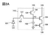
- 2A and 2B are diagrams illustrating a pixel circuit
- FIG. 2C is a diagram illustrating a memory circuit.
- FIG. 3A is a diagram for explaining the rolling shutter system
- FIG. 3B is a diagram for explaining the global shutter system.
- 4A and 4B are timing charts for explaining the operation of the pixel circuit.
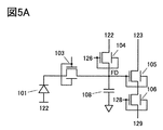
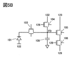
- 5A and 5B are diagrams illustrating a pixel circuit.
- 6A to 6C are block diagrams illustrating the imaging device.
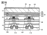
- 7A and 7B are cross-sectional views illustrating the configuration of the imaging device.
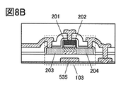
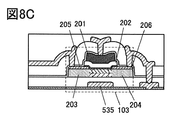
- 8A to 8D are diagrams illustrating transistors.
- FIG. 9 is a diagram illustrating a configuration example of a storage device.
- FIG. 9 is a diagram illustrating a configuration example of a storage device.
- FIG. 10 is a diagram illustrating a configuration example of a memory cell array.
- FIG. 11A is a circuit diagram illustrating a configuration example of a memory cell in FIGS. 11A to 11D.
- FIG. 12 is a cross-sectional view showing the structure of the semiconductor device.
- FIG. 13 is a cross-sectional view showing the structure of the semiconductor device.
- 14A to 14F are perspective views illustrating a package including an image pickup device and a camera module.
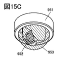
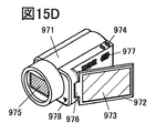
- 15A to 15F are diagrams illustrating electronic devices.
- the element may be composed of a plurality of elements.
- a plurality of transistors which operate as switches may be connected in series or in parallel.
- the capacitor may be divided and placed at a plurality of positions.
- one conductor may have a plurality of functions such as wiring, an electrode, and a terminal in some cases, and in this specification, a plurality of names may be used for the same element.
- a plurality of names may be used for the same element.
- the elements may actually be connected through a plurality of conductors, and In the book, such a configuration is included in the category of direct connection.
- One embodiment of the present invention is an imaging device having a memory function. By temporarily storing the image pickup data in the memory circuit, the image pickup data can be continuously acquired at high speed. Further, the imaging data can be read out from the memory circuit at high speed, and data analysis can be performed at high speed.
- a transistor including a metal oxide in a channel formation region (hereinafter referred to as an OS transistor) is used for a circuit included in a pixel.
- the OS transistor can be formed over a silicon substrate, so that a bonding process can be reduced.
- FIG. 1 is a diagram illustrating an imaging device of one embodiment of the present invention.
- the imaging device has a layer 12, a layer 13, and a layer 14.
- the layer 13 is provided between the layer 12 and the layer 14 and has a region where they overlap with each other.
- the layer 12 includes a photoelectric conversion device (also referred to as a photoelectric conversion element).
- a photodiode can be used as the photoelectric conversion device.
- the photodiode for example, a pn junction photodiode using single crystal silicon for a photoelectric conversion portion, a pin photodiode using amorphous silicon, polycrystalline silicon, or microcrystalline silicon for a photoelectric conversion layer is used. be able to.
- a material such as a compound semiconductor, selenium, or a selenium compound may be used for the photoelectric conversion layer.
- a pn junction photodiode using single crystal silicon will be described.
- the layer 13 includes a transistor included in a pixel circuit, a transistor included in a memory circuit, and the like. Further, it is preferable to use an OS transistor as the transistor.
- the OS transistor has a characteristic of extremely low off-state current and is suitable as a component element of a pixel circuit because data can be held in the pixel circuit for a long time.
- the memory circuit can store digital data output from the first reading circuit described below.
- the layer 14 has a transistor and the like included in the first read circuit and a transistor and the like included in the second read circuit.
- the first readout circuit can include, for example, an A/D converter that converts analog data output from the pixel circuit into digital data.
- the second read circuit can include, for example, a sense amplifier for reading data stored in the memory circuit.
- FIG. 2A is a diagram illustrating an example of a pixel circuit.
- the pixel circuit includes the photoelectric conversion device 101 included in the layer 12 and the circuit 110 included in the layer 13.
- the circuit 110 can include the transistor 103, the transistor 104, the transistor 105, the transistor 106, and the capacitor 108. Note that the capacitor 108 may not be provided.
- One electrode (cathode) of the photoelectric conversion device 101 is electrically connected to one of a source and a drain of the transistor 103.
- the other of the source and the drain of the transistor 103 is electrically connected to one of the source and the drain of the transistor 104.
- One of a source and a drain of the transistor 104 is electrically connected to one electrode of the capacitor 108.
- One electrode of the capacitor 108 is electrically connected to the gate of the transistor 105.
- One of a source and a drain of the transistor 105 is electrically connected to one of a source and a drain of the transistor 106.
- a wiring that connects the other of the source and the drain of the transistor 103, one electrode of the capacitor 108, and the gate of the transistor 105 is referred to as a node FD.
- the node FD can function as a charge storage unit.
- the other electrode (anode) of the photoelectric conversion device 101 is electrically connected to the wiring 121.
- the gate of the transistor 103 is electrically connected to the wiring 127.
- the other of the source and the drain of the transistor 104 is electrically connected to the wiring 122.
- the other of the source and the drain of the transistor 105 is electrically connected to the wiring 123.
- the gate of the transistor 104 is electrically connected to the wiring 126.
- the gate of the transistor 106 is electrically connected to the wiring 128.
- the other electrode of the capacitor 108 is electrically connected to a reference potential line such as a GND wiring.
- the other of the source and the drain of the transistor 106 is electrically connected to the wiring 129.
- the wirings 127, 126, and 128 can have a function as a signal line which controls conduction of each transistor.
- the wiring 129 can have a function as an output line.
- the wirings 121, 122, and 123 can have a function as power supply lines.
- the cathode side of the photoelectric conversion device 101 is electrically connected to the transistor 103 and the node FD is reset to a high potential to operate, so that the wiring 122 is at a higher potential (than the wiring 121. Also high potential).
- FIG. 2A shows a configuration in which the cathode of the photoelectric conversion device 101 is electrically connected to the node FD, but the anode side of the photoelectric conversion device 101 is electrically connected to one of the source and the drain of the transistor 103 as shown in FIG. 2B. It may be configured to be connected.
- the wiring 122 since the node FD is reset to a low potential to operate, the wiring 122 has a low potential (a potential lower than that of the wiring 121).
- the transistor 103 has a function of controlling the potential of the node FD.
- the transistor 104 has a function of resetting the potential of the node FD.
- the transistor 105 functions as a source follower circuit and can output the potential of the node FD as image data to the wiring 129.
- the transistor 106 has a function of selecting a pixel which outputs image data.
- OS transistors are preferably used as the transistors 103 and 104.
- the OS transistor has a characteristic of extremely low off-state current.
- OS transistors for the transistors 103 and 104 the period in which electric charge can be held in the node FD can be extremely extended. Therefore, it is possible to apply the global shutter method in which charges are simultaneously stored in all pixels without complicating the circuit configuration and the operating method.
- FIG. 3A is a schematic diagram of a rolling shutter system operation method
- FIG. 3B is a schematic diagram of a global shutter system.
- En represents the exposure (accumulation operation) of the nth column (n is a natural number)
- Rn represents the readout operation of the nth column.
- 3A and 3B show the operation from the first row to the M-th row (M is a natural number).
- the rolling shutter method is an operation method of sequentially performing exposure and reading of data, and is a method of overlapping a reading period of a certain row and an exposure period of another row. Since the read operation is performed immediately after exposure, it is possible to perform imaging even with a circuit configuration in which the data retention period is relatively short. However, since the image of one frame is composed of the data having no simultaneity of image capturing, the image is distorted when capturing a moving object.
- the global shutter method is an operation method in which all pixels are exposed at the same time, data is held in each pixel, and data is read for each row. Therefore, it is possible to obtain an image without distortion even when capturing a moving object.
- a rolling shutter method is often used because a data potential easily flows out from a charge storage portion.
- Si transistor a transistor using Si for a channel formation region
- a rolling shutter method is often used because a data potential easily flows out from a charge storage portion.
- the imaging device of one embodiment of the present invention can also be operated by a rolling shutter method.
- an OS transistor and a Si transistor may be arbitrarily combined and applied to the transistors included in the pixel circuit. Further, all the transistors may be OS transistors or Si transistors.
- the Si transistor a transistor including amorphous silicon, a transistor including crystalline silicon (typically, low temperature polysilicon, single crystal silicon, or the like) can be given.
- FIG. 2C is a diagram illustrating an example of a cell of the memory circuit included in the layer 13.
- the cell 111 has a transistor 107 and a capacitor 109.
- One of a source and a drain of the transistor 107 is electrically connected to one electrode of the capacitor 109.
- the other of the source and the drain of the transistor 107 is electrically connected to the wiring 132.
- the gate of the transistor 107 is electrically connected to the wiring 132. Note that cells having other configurations can also be used.
- the wiring 131 can have a function as a word line.
- the wiring 132 can have a function as a bit line.
- An OS transistor is preferably used as the transistor 107. As described above, since the off-state current of the OS transistor is extremely small, the charge accumulated in the capacitor 109 can be held for a long time. Therefore, the refresh interval can be extended and the power consumption can be reduced. It can also be used as a substantially non-volatile memory. Details of the memory circuit will be described in another embodiment described later.
- the transistor 104 is turned off and the supply of the reset potential is cut off.
- the potential of the node FD decreases according to the operation of the photoelectric conversion device 101 (accumulation operation).
- the transistor 103 is turned off and the potential of the node FD is determined and held. (Holding operation). At this time, by using an OS transistor having a low off-state current as the transistors 103 and 104 connected to the node FD, unnecessary charge can be prevented from flowing out from the node FD and data retention time can be extended. it can.
- the pixel circuit illustrated in FIG. 2B can be operated according to the timing chart in FIG. 4B. Note that “H” is constantly supplied to the wirings 121 and 123, and “L” is constantly supplied to the wiring 122. The basic operation is similar to the description of the timing chart of FIG. 2A above.
- a transistor may be provided with a back gate as illustrated in FIGS. 5A and 5B.
- FIG. 5A shows a configuration in which the back gate is electrically connected to the front gate, which has the effect of increasing the on-current.
- FIG. 5B shows a structure in which the back gate is electrically connected to a wiring which can supply a constant potential, and the threshold voltage of the transistor can be controlled.
- each transistor can perform an appropriate operation, such as combining FIGS. 5A and 5B, may be employed.
- the pixel circuit may include a transistor in which a back gate is not provided.
- FIG. 6A is a block diagram illustrating an imaging device of one embodiment of the present invention.
- the imaging device has a pixel array 51 having pixel circuits 50 arranged in a matrix, a circuit 52 (row driver) having a function of selecting a row of the pixel array 51, and a function of reading data from the pixel circuit 50. It has a circuit 53, a circuit 57 for supplying a reset potential and a power supply potential, a circuit 58 for storing output data of the circuit 53, and a circuit 59 having a function of reading data from the circuit 58.
- the circuit 53 includes a circuit 54 (column driver) having a function of selecting a column of the pixel array 51, a circuit 55 (CDS circuit) for performing correlated double sampling processing on output data of the pixel circuit 50, and a circuit.
- a circuit 56 (A/D converter) having a function of converting analog data output from 55 into digital data can be included.
- a shift register circuit or a decoder circuit can be used for the circuits 52 and 54.
- 6B and 6C are conceptual diagrams for explaining the arrangement of each circuit and the circuits shown in FIGS. 2A, 2B, and 2C in the laminated structure of the imaging device shown in FIG.
- the photoelectric conversion device 101 is provided in the layer 12, and the pixel circuit 50 is formed by being electrically connected to the circuit 110 provided in the layer 13. Further, the circuit 58 is provided in the layer 13.
- the circuit 110 and the circuit 58 can be arranged side by side in the horizontal direction as shown in FIG. 6B. Since the circuit 110 and the circuit 58 are formed using OS transistors, they can be manufactured in the same step.
- the circuit 110 and the circuit 58 may be stacked and arranged in the vertical direction as illustrated in FIG. 6C. Since the OS transistor can be formed using a thin film, stacking is easy. By stacking the circuits 110 and 58, the pixel circuits 50 and the cells 111 can be arranged at high density, and resolution and storage capacity can be improved. Note that the cell 111 is not limited to a single layer and may be a stack of a plurality of layers.
- the layer 14 can be provided with the circuits 52, 53, 59, and the like. Since these circuits are desired to operate at high speed, they are preferably formed using Si transistors. That is, layer 14 preferably comprises a single crystal silicon substrate. Note that the circuit 52 may be formed with an OS transistor. In this case, the circuit 52 is provided in the layer 12.
- some of the transistors included in each of the circuit 52, the circuit 53, and the circuit 59 may be OS transistors provided in the layer 13.
- some of the transistors included in each of the circuit 110 and the circuit 58 may be formed of a Si transistor provided in the layer 14.
- image pickup and data processing can be performed at high speed.
- a circuit including an OS transistor can be stacked over a circuit including a Si transistor, so that the imaging device can be downsized.
- This embodiment can be implemented in appropriate combination with any of the structures described in the other embodiments and the like.
- FIG. 7A is a diagram illustrating an example of a cross section including a pixel region.
- the structure can be manufactured by forming the layer 13 over the layer 12 and attaching the separately formed layer 14 to the layer 13. In addition, an electrically connecting portion between the layers 13 and 14 is omitted.
- a pn including a region 22 having an n-type conductivity type, a region having a p-type conductivity type (single crystal silicon substrate 21), and a region 28 having a p + -type conductivity type.
- a junction photodiode is provided.
- FIG. 7A An OS transistor is provided in the layer 13.
- the transistor 103 and the transistor 107 are illustrated using the circuit configurations illustrated in FIGS. 2A, 2B, and 2C as examples.
- the layer 14 is provided with a silicon substrate 25 having Si transistors or the like.
- 7A illustrates the transistor 112 included in the circuit 53 and the transistor 113 included in the circuit 59.
- Insulating layers 65 and 66 are provided between the region where the OS transistor is formed and the region where the Si device (photoelectric conversion device 101, Si transistor, or the like) is formed.
- the insulating layers 65 and 66 have a function of preventing hydrogen diffusion.
- hydrogen in the insulating layer provided in the vicinity of the photoelectric conversion device 101 terminates a dangling bond of silicon.
- hydrogen in the insulating layer provided in the vicinity of the channel formation regions of the transistors 103 and 107 is one of the factors that generate carriers in the oxide semiconductor layer.
- the insulating layers 65 and 66 can improve the reliability of the Si device by confining hydrogen in one layer. Further, the diffusion of hydrogen from one layer to the other layer is suppressed, so that the reliability of the transistors 103 and 107 can be improved.
- the insulating layers 65 and 66 for example, aluminum oxide, aluminum oxynitride, gallium oxide, gallium oxynitride, yttrium oxide, yttrium oxynitride, hafnium oxide, hafnium oxynitride, yttria-stabilized zirconia (YSZ), or the like can be used. it can.
- An insulating layer 31 is provided on the layer 13 side in the bonding region between the layers 13 and 14. Further, the insulating layer 33 is provided on the layer 14 side.
- the insulating layer 31 and the insulating layer 33 are insulating layers that contribute to bonding.
- FIG. 7A shows an example in which the insulating layer 31 has two layers, that is, the insulating layer 63 and the insulating layer 64.
- the insulating layer 63 an organic film such as acrylic resin or polyimide can be used.
- An inorganic film such as a silicon oxide film can be used for the insulating layers 33 and 64.
- FIG. 7B shows a structural example different from that of FIG. 7A.
- the structure can be manufactured by forming the layer 13 over the layer 14 and attaching the separately formed layer 12 to the layer 13.
- an electrically connecting portion between the layers 13 and 14 is omitted.
- the insulating layer 33 and the conductive layer 34 are provided on the layer 12 side in the junction region between the layers 12 and 13. Further, the insulating layer 31 and the conductive layer 32 are provided on the layer 13 side.
- the example in which the insulating layer 31 is three layers of the insulating layer 63, the insulating layer 65, and the insulating layer 64 is shown.
- the insulating layer 65 may be provided at other positions as long as the above effects can be obtained.
- the insulating layer 63 and the insulating layer 65 may be replaced with each other.
- an electrical connection can be obtained by attaching the conductive layer 34 and the conductive layer 32 to each other.
- FIG. 8A shows details of the OS transistor.
- the OS transistor illustrated in FIG. 8A has a self-aligned structure in which an insulating layer is provided over a stack of an oxide semiconductor layer and a conductive layer and a groove reaching the semiconductor layer is provided to form a source electrode 205 and a drain electrode 206. is there.
- the OS transistor can include a channel formation region formed in the oxide semiconductor layer 207, a source region 203, and a drain region 204, as well as a gate electrode 201 and a gate insulating film 202. At least the gate insulating film 202 and the gate electrode 201 are provided in the groove. An oxide semiconductor layer 208 may be further provided in the groove.
- the OS transistor may have a self-aligned structure in which the source region 203 and the drain region 204 are formed in the semiconductor layer with the gate electrode 201 as a mask.
- a non-self-aligned top-gate transistor having a region where the source electrode 205 or the drain electrode 206 and the gate electrode 201 overlap with each other may be used.
- the transistors 103, 105, and 106 have a structure including the back gate 535
- the transistors 103, 105, and 106 may have a structure without the back gate.
- the back gate 535 may be electrically connected to the front gates of the transistors provided to face each other as in the cross-sectional view in the channel width direction of the transistor illustrated in FIG. 8D. Note that although FIG. 8D shows a cross section taken along the line A1-A2 of the transistor 103 in FIG. 8A, the front gate and the back gate 535 may be similarly electrically connected to each other in a transistor having another structure. Further, the back gate 535 may have a structure capable of supplying a fixed potential different from that of the front gate.
- a metal oxide having an energy gap of 2 eV or more, preferably 2.5 eV or more, more preferably 3 eV or more can be used.
- an oxide semiconductor containing indium or the like can be used, and for example, CAAC-OS or CAC-OS described later can be used.
- the CAAC-OS has stable atoms forming a crystal and is suitable for a transistor in which reliability is important. Further, since the CAC-OS exhibits high mobility characteristics, it is suitable for a transistor or the like which drives at high speed.
- the OS transistor Since the OS transistor has a large energy gap in the semiconductor layer, it exhibits extremely low off-current characteristics of several yA/ ⁇ m (current value per 1 ⁇ m of channel width). Further, the OS transistor has characteristics different from those of the Si transistor such that impact ionization, avalanche breakdown, short channel effect, and the like do not occur, and a circuit with high withstand voltage and high reliability can be formed. Further, variations in electrical characteristics due to non-uniformity of crystallinity, which is a problem in Si transistors, are less likely to occur in OS transistors.
- the semiconductor layer included in the OS transistor is an In-M-Zn-based oxide containing indium, zinc, and M (a metal such as aluminum, titanium, gallium, germanium, yttrium, zirconium, lanthanum, cerium, tin, neodymium, or hafnium).
- the film can be represented by.
- the In-M-Zn-based oxide can be formed using, for example, a sputtering method, an ALD (Atomic Layer Deposition) method, or a MOCVD (Metal Organic Chemical Vapor Deposition) method.
- the atomic ratio of metal elements in the sputtering target preferably satisfies In?M and Zn?M.
- the atomic ratio of the semiconductor layers to be formed includes a fluctuation of ⁇ 40% in the atomic ratio of the metal element contained in the sputtering target.
- an oxide semiconductor having a low carrier density is used for the semiconductor layer.
- the semiconductor layer has a carrier density of 1 ⁇ 10 17 /cm 3 or less, preferably 1 ⁇ 10 15 /cm 3 or less, more preferably 1 ⁇ 10 13 /cm 3 or less, and more preferably 1 ⁇ 10 11 /cm 3. 3 or less, more preferably less than 1 ⁇ 10 10 /cm 3 , and 1 ⁇ 10 ⁇ 9 /cm 3 or more of an oxide semiconductor can be used.
- Such an oxide semiconductor is referred to as a highly purified intrinsic or substantially highly purified intrinsic oxide semiconductor. It can be said that the oxide semiconductor has a low density of defect states and stable characteristics.
- the composition is not limited to these, and a material having an appropriate composition may be used depending on required semiconductor characteristics and electric characteristics of a transistor (field-effect mobility, threshold voltage, or the like). Further, in order to obtain the required semiconductor characteristics of the transistor, it is preferable that the carrier density, the impurity concentration, the defect density, the atomic ratio of metal element to oxygen, the interatomic distance, the density, and the like of the semiconductor layer be appropriate. ..
- the concentration of silicon or carbon in the semiconductor layer (the concentration obtained by secondary ion mass spectrometry) is 2 ⁇ 10 18 atoms/cm 3 or less, preferably 2 ⁇ 10 17 atoms/cm 3 or less.
- the alkali metal and the alkaline earth metal might generate carriers when combined with the oxide semiconductor, which might increase the off-state current of the transistor. Therefore, the concentration of alkali metal or alkaline earth metal in the semiconductor layer (concentration obtained by secondary ion mass spectrometry) is 1 ⁇ 10 18 atoms/cm 3 or less, preferably 2 ⁇ 10 16 atoms/cm 3 or less.
- the nitrogen concentration in the semiconductor layer is preferably 5 ⁇ 10 18 atoms/cm 3 or less.
- oxygen when hydrogen is contained in the oxide semiconductor included in the semiconductor layer, oxygen reacts with oxygen which is bonded to a metal atom to be water, which might cause oxygen vacancies in the oxide semiconductor.
- the transistor When the channel formation region in the oxide semiconductor contains oxygen vacancies, the transistor might have normally-on characteristics.
- a defect in which hydrogen is contained in an oxygen vacancy may function as a donor and an electron which is a carrier may be generated.
- part of hydrogen may be bonded to oxygen which is bonded to a metal atom to generate an electron which is a carrier. Therefore, a transistor including an oxide semiconductor which contains a large amount of hydrogen is likely to have normally-on characteristics.
- a defect in which hydrogen is contained in an oxygen vacancy can function as a donor of an oxide semiconductor.
- the oxide semiconductor may be evaluated not by the donor concentration but by the carrier concentration. Therefore, in this specification and the like, a carrier concentration which is assumed to be a state where no electric field is applied may be used as a parameter of the oxide semiconductor, instead of the donor concentration. That is, the “carrier concentration” described in this specification and the like can be called the “donor concentration” in some cases.
- the hydrogen concentration obtained by secondary ion mass spectrometry is less than 1 ⁇ 10 20 atoms/cm 3 , preferably 1 ⁇ 10 19 atoms/cm 3. It is less than 3 , more preferably less than 5 ⁇ 10 18 atoms/cm 3 , and even more preferably less than 1 ⁇ 10 18 atoms/cm 3 .
- the oxide semiconductor is divided into a single crystal oxide semiconductor and a non-single crystal oxide semiconductor other than the single crystal oxide semiconductor.
- non-single-crystal oxide semiconductors include CAAC-OS (C-Axis Aligned Crystalline Oxide Semiconductor), polycrystalline oxide semiconductors, nc-OS (nanocrystal Oxide Semiconductor), and pseudo-amorphous oxide semiconductors (a-like oxide semiconductors).
- OS amorphous-like oxide (Semiconductor), and amorphous oxide semiconductor.
- the amorphous structure has the highest defect level density and the CAAC-OS has the lowest defect level density.
- the oxide semiconductor film having an amorphous structure has disordered atomic arrangement and no crystalline component, for example.
- the oxide film having an amorphous structure has, for example, a completely amorphous structure and has no crystal part.
- the semiconductor layer may be a mixed film including two or more kinds of an amorphous structure region, a microcrystalline structure region, a polycrystalline structure region, a CAAC-OS region, and a single crystal structure region.
- the mixed film may have, for example, a single-layer structure or a laminated structure including any two or more kinds of the above-mentioned regions.
- CAC Cloud-Aligned Composite
- the CAC-OS is a structure of a material in which an element included in an oxide semiconductor is unevenly distributed at a size of 0.5 nm to 10 nm inclusive, preferably 1 nm to 2 nm inclusive, or in the vicinity thereof.
- an oxide semiconductor one or more metal elements are unevenly distributed and a region including the metal element has a size of 0.5 nm to 10 nm, preferably 1 nm to 2 nm, or a size in the vicinity thereof.
- the state of being mixed with is also called a mosaic shape or a patch shape.
- the oxide semiconductor preferably contains at least indium. It is particularly preferable to contain indium and zinc. In addition to them, aluminum, gallium, yttrium, copper, vanadium, beryllium, boron, silicon, titanium, iron, nickel, germanium, zirconium, molybdenum, lanthanum, cerium, neodymium, hafnium, tantalum, tungsten, magnesium, etc. One kind or plural kinds selected from the above may be contained.
- CAC-OS in In-Ga-Zn oxide (In-Ga-Zn oxide among CAC-OS may be particularly referred to as CAC-IGZO) means indium oxide (hereinafter, InO).
- InO indium oxide
- X1 X1 is a real number larger than 0
- In X2 Zn Y2 O Z2 X2, Y2, and Z2 are real numbers larger than 0
- gallium indium oxide (hereinafter, InO).
- GaO X3 (X3 is a real number larger than 0)
- gallium zinc oxide hereinafter, Ga X4 Zn Y4 O Z4 (X4, Y4, and Z4 are real numbers larger than 0)
- InO X1 or In X2 Zn Y2 O Z2 having a mosaic shape is uniformly distributed in the film (hereinafter, also referred to as cloud shape). is there.
- the CAC-OS is a composite oxide semiconductor having a structure in which a region containing GaO X3 as a main component and a region containing In X2 Zn Y2 O Z2 or InO X1 are mixed.
- the atomic ratio of In to the element M in the first region is larger than the atomic ratio of In to the element M in the second region. It is assumed that the concentration of In is higher than that in the region of No. 2.
- IGZO is a common name and may refer to one compound of In, Ga, Zn, and O.
- InGaO 3 (ZnO) m1 (m1 is a natural number) or In (1+x0) Ga (1-x0) O 3 (ZnO) m0 (-1 ⁇ x0 ⁇ 1, m0 is an arbitrary number) is represented.
- Crystalline compounds may be mentioned.
- the crystalline compound has a single crystal structure, a polycrystalline structure, or a CAAC structure.
- the CAAC structure is a crystal structure in which a plurality of IGZO nanocrystals has c-axis orientation and is connected without being oriented in the ab plane.
- the nanocrystal is basically a hexagon, but is not limited to a regular hexagon, and may be a non-regular hexagon.
- the strain may have a lattice arrangement such as a pentagon and a heptagon.
- a clear crystal grain boundary also referred to as a grain boundary
- the formation of crystal grain boundaries is suppressed by the distortion of the lattice arrangement. This is because the CAAC-OS can tolerate strain due to the fact that the arrangement of oxygen atoms is not dense in the ab plane direction, the bond distance between atoms changes due to substitution with a metal element, or the like. It is thought to be because.
- the CAAC-OS in which clear crystal grain boundaries are not confirmed is one of crystalline oxides having a crystal structure suitable for a semiconductor layer of a transistor.
- a structure containing Zn is preferable for forming the CAAC-OS.
- In-Zn oxide and In-Ga-Zn oxide are preferable because they can suppress generation of crystal grain boundaries more than In oxide.
- CAC-OS relates to a material structure of an oxide semiconductor.
- CAC-OS refers to a region that is observed in the form of nanoparticles mainly containing Ga as a part and nanoparticles mainly containing In as a part in a material structure containing In, Ga, Zn, and O.
- the regions that are observed in a pattern mean that the regions are randomly dispersed in a mosaic pattern. Therefore, in CAC-OS, the crystal structure is a secondary element.
- the CAC-OS does not include a stacked structure of two or more kinds of films having different compositions.
- a structure including two layers of a film containing In as a main component and a film containing Ga as a main component is not included.
- the CAC-OS has a region that is observed in the form of nanoparticles partially containing the metal element as a main component and a nanoparticle mainly containing In as a main component. The areas observed in the form of particles are randomly dispersed in a mosaic shape.
- the CAC-OS can be formed by a sputtering method under the condition that the substrate is not heated intentionally, for example.
- a sputtering method one or more selected from an inert gas (typically argon), an oxygen gas, and a nitrogen gas may be used as a film formation gas.
- an inert gas typically argon
- oxygen gas typically argon
- a nitrogen gas may be used as a film formation gas.
- the flow rate ratio of the oxygen gas is 0% or more and less than 30%, preferably 0% or more and 10% or less. ..
- the CAC-OS is characterized in that no clear peak is observed when it is measured using a ⁇ /2 ⁇ scan by an Out-of-plane method, which is one of the X-ray diffraction (XRD) measurement methods. Have. That is, it can be seen from the X-ray diffraction measurement that the orientations in the ab plane direction and the c-axis direction of the measurement region are not seen.
- XRD X-ray diffraction
- the electron beam diffraction pattern of the CAC-OS which is obtained by irradiating an electron beam with a probe diameter of 1 nm (also referred to as a nanobeam electron beam), a ring-shaped region having high brightness (ring region) and the ring are formed. Multiple bright spots are observed in the area. Therefore, it can be seen from the electron diffraction pattern that the crystal structure of CAC-OS has an nc (nano-crystal) structure having no orientation in the planar direction and the cross-sectional direction.
- nc nano-crystal
- GaO X3 is a main component by EDX mapping obtained using energy dispersive X-ray spectroscopy (EDX: Energy Dispersive X-ray spectroscopy). It can be confirmed that the region and the region containing In X2 Zn Y2 O Z2 or InO X1 as main components are unevenly distributed and mixed.
- the CAC-OS has a structure different from that of the IGZO compound in which the metal element is uniformly distributed, and has a property different from that of the IGZO compound. That is, in the CAC-OS, a region containing GaO X3 or the like as its main component and a region containing In X2 Zn Y2 O Z2 , or InO X1 as its main component are phase-separated from each other, and a region containing each element as its main component. Has a mosaic structure.
- the region containing In X2 Zn Y2 O Z2 or InO X1 as a main component is a region having higher conductivity than the region containing GaO X3 or the like as a main component. That, In X2 Zn Y2 O Z2 or InO X1, is an area which is the main component, by carriers flow, expressed the conductivity of the oxide semiconductor. Therefore, a region in which In X2 Zn Y2 O Z2 or InO X1 is a main component is distributed in the oxide semiconductor in a cloud shape, whereby high field-effect mobility ( ⁇ ) can be realized.
- the region containing GaO X3 or the like as the main component has a higher insulating property than the region containing In X2 Zn Y2 O Z2 or InO X1 as the main component. That is, since the region containing GaO X3 or the like as a main component is distributed in the oxide semiconductor, leakage current can be suppressed and favorable switching operation can be realized.
- the CAC-OS when used for a semiconductor device, the insulating property due to GaO X3 and the like and the conductivity due to In X2 Zn Y2 O Z2 , or InO X1 are high due to complementary action.
- On-current (I on ) and high field-effect mobility ( ⁇ ) can be realized.
- the semiconductor device using the CAC-OS has high reliability. Therefore, the CAC-OS is suitable as a constituent material of various semiconductor devices.
- the insulating layer 33 and the conductive layer 34 are provided on the layer 12.
- the conductive layer 34 is embedded in the insulating layer 33 and has a region penetrating therethrough.
- the conductive layer 34 is electrically connected to the region 22.
- the surfaces of the insulating layer 33 and the conductive layer 34 are flattened so that their heights match.
- the layer 13 is provided with an insulating layer 31 and a conductive layer 32.
- the conductive layer 32 is embedded in the insulating layer 31 and has a region penetrating therethrough.
- the conductive layer 32 is electrically connected to the transistor 103.
- the surfaces of the insulating layer 31 and the conductive layer 32 are flattened so that their heights match.
- the conductive layers 32 and 34 are made of the same metal element as the main component.
- the surfaces of the insulating layer 31 and the insulating layer 33 are preferably composed of the same component.
- the conductive layers 32 and 34 Cu, Al, Sn, Zn, W, Ag, Pt, or Au can be used.
- Cu, Al, W, or Au is preferably used.
- an insulating film in which silicon oxide, silicon oxynitride, silicon nitride oxide, silicon nitride, titanium nitride, or the like is stacked on the surface can be used for the insulating films 31 and 33.
- connection between the conductive layer 32 and the conductive layer 34 can be obtained. Further, a connection having mechanical strength of the insulating layer 31 and the insulating layer 33 can be obtained.
- a surface activated joining method can be used for joining the metal layers to each other in which the oxide film on the surface and the adsorbed layer of impurities are removed by sputtering or the like, and the cleaned and activated surfaces are brought into contact with each other for joining. ..
- a diffusion bonding method or the like in which the surfaces are bonded together by using both temperature and pressure can be used. In both cases, bonding at the atomic level occurs, so that excellent bonding can be obtained not only electrically but mechanically.
- the surfaces that have been subjected to hydrophilic treatment with oxygen plasma or the like are brought into contact with each other to temporarily join, and then main joining is performed by dehydration by heat treatment.
- a joining method or the like can be used. Also in the hydrophilic bonding method, bonding at the atomic level occurs, so that mechanically excellent bonding can be obtained.
- the surface activation joining method and the hydrophilic joining method may be combined.
- a method may be used in which the surface is cleaned after polishing, the surface of the metal layer is subjected to an antioxidant treatment, and then a hydrophilic treatment is performed to bond the metal layer.
- the surface of the metal layer may be made of a non-oxidizing metal such as Au and subjected to a hydrophilic treatment.
- the configuration of the image pickup device can be used for the image sensor chip.
- FIG. 14A is an external perspective view of the upper surface side of the package including the image sensor chip.
- the package has a package substrate 610 for fixing the image sensor chip 650, a cover glass 620, an adhesive 630 for bonding the both, and the like.
- FIG. 14C is an external perspective view of the lower surface side of the package.
- a BGA Bit Grid Array
- LGA Land Grid Array
- PGA Peripheral Component Interconnect
- FIG. 14E is a perspective view of the package in which the cover glass 620 and the adhesive 630 are partially omitted. Electrode pads 660 are formed on the package substrate 610, and the electrode pads 660 and the bumps 640 are electrically connected via the through holes. The electrode pad 660 is electrically connected to the image sensor chip 650 by a wire 670.
- FIG. 14B is an external perspective view of the upper surface side of the camera module in which the image sensor chip is housed in a lens-integrated package.
- the camera module includes a package substrate 611 that fixes the image sensor chip 651, a lens cover 621, a lens 635, and the like. Further, an IC chip 690 having a function such as a drive circuit and a signal conversion circuit of the image pickup device is also provided between the package substrate 611 and the image sensor chip 651, and has a configuration as SiP (System in Package). There is.
- FIG. 14D is an external perspective view of the lower surface side of the camera module.
- the lower surface and the side surface of the package substrate 611 have a QFN (Quad Flat No-lead package) configuration in which mounting lands 641 are provided.
- QFN Quad Flat No-lead package
- the configuration is an example, and a QFP (Quad Flat Package) or the BGA described above may be provided.
- FIG. 14F is a perspective view of the module illustrated by omitting a part of the lens cover 621 and the lens 635.
- the land 641 is electrically connected to the electrode pad 661, and the electrode pad 661 is electrically connected to the image sensor chip 651 or the IC chip 690 by the wire 671.
- the image sensor chip By mounting the image sensor chip in the package having the above-described form, mounting on a printed circuit board or the like becomes easy, and the image sensor chip can be incorporated in various semiconductor devices and electronic devices.
- This embodiment can be implemented in appropriate combination with any of the structures described in the other embodiments and the like.
- FIG. 9 is a block diagram showing a configuration example of a storage device.
- the memory device 3300 includes a peripheral circuit 3311, a cell array (Cell Array) 3401, and a semiconductor device 3100. Note that the memory device 3300 corresponds to the circuit 58 described in Embodiment 1.
- a low power supply voltage (VSS), a high power supply voltage (VDD) for the peripheral circuit 3311, and a high power supply voltage (VIL) for the cell array 3401 are externally supplied to the memory device 3300 as power supply voltages.
- control signal CE, WE, RE
- address signal ADDR an address signal
- data signal WDATA is input to the input/output circuit 3334.
- the peripheral circuit 3311 includes a row decoder 3321, a word line driver circuit 3322, a column decoder 3331, a bit line driver circuit 3330, an output circuit 3340, and a control logic circuit 3360.
- the word line driver circuit 3322 has a function of supplying a potential to the wiring WL.
- the bit line driver circuit 3330 includes a precharge circuit 3332, an amplifier circuit 3333, and an input/output circuit 3334.
- the precharge circuit 3332 has a function of precharging the wiring SL (not illustrated), the wiring BIL, the wiring RBL, or the like.
- the amplifier circuit 3333 has a function of amplifying a data signal read from the wiring BIL or the wiring RBL. Note that the wiring WL, the wiring SL, the wiring BIL, and the wiring RBL are wirings connected to a memory cell (Memory Cell) 3411 included in the cell array 3401, which will be described in detail later.
- the amplified data signal is output to the outside of the storage device 3300 as a digital data signal RDATA via the output circuit 3340.
- the control logic circuit 3360 processes an input signal (CE, WE, RE) from the outside to generate a control signal for the row decoder 3321 and the column decoder 3331.
- CE is a chip enable signal
- WE is a write enable signal
- RE is a read enable signal.
- the signal processed by the control logic circuit 3360 is not limited to this, and another control signal may be input as necessary.
- each circuit or each signal described above can be appropriately discarded as necessary.
- An OS transistor can be applied to the transistors included in the cell array 3401. Further, an OS transistor can be used as a transistor included in the peripheral circuit 3311. By forming the cell array 3401 and the peripheral circuit 3311 using OS transistors, the cell array 3401 and the peripheral circuit 3311 can be manufactured in the same manufacturing process, so that manufacturing cost can be suppressed low.
- the cell array 3401 includes m (m is an integer of 1 or more) in one column and n (n is an integer of 1 or more) in one row, which is a total of m ⁇ n memory cells 3411.
- the cells 3411 are arranged in a matrix.
- the address of the memory cell 3411 is also shown.
- [1,1] indicates the memory cell 3411 located at the address of the first row and the first column
- [i,j] (i is an integer of 1 or more and m or less, and j is 1 or more and n or more).
- the following integers) indicate the memory cell 3411 located at the address of the i-th row and the j-th column.
- the number of wirings connecting the cell array 3401 and the word line driver circuit 3322 is determined by the structure of the memory cell 3411, the number of memory cells 3411 included in one column, and the like.
- the number of wirings connecting the cell array 3401 and the bit line driver circuit 3330 is determined by the structure of the memory cell 3411, the number of memory cells 3411 included in one row, and the like.
- FIG. 11 shows a configuration example of the memory cells 3411A to 3411D which can be applied to the above memory cell 3411.
- FIG. 11A shows a circuit configuration example of the DRAM type memory cell 3411A.
- a DRAM including an OS transistor is referred to as a DOSRAM (Dynamic Oxide Semiconductor Random Access Memory).
- the memory cell 3411A includes a transistor M11 and a capacitor Cs.
- the first terminal of the transistor M11 is connected to the first terminal of the capacitor Cs
- the second terminal of the transistor M11 is connected to the wiring BIL
- the gate of the transistor M11 is connected to the wiring WL
- the back gate of the transistor M11 is , And is connected to the wiring BGL.
- the second terminal of the capacitor Cs is connected to the wiring GNDL.
- the wiring GNDL is a wiring which gives a low-level potential (sometimes referred to as a reference potential).
- the wiring BIL functions as a bit line and the wiring WL functions as a word line.
- the wiring BGL functions as a wiring for applying a potential to the back gate of the transistor M11.
- the wiring BGL is electrically connected to the output terminal OUT of the semiconductor device 3100. By applying an arbitrary potential to the wiring BGL, the threshold voltage of the transistor M11 can be increased or decreased.
- Data writing and reading are performed by applying a high-level potential to the wiring WL, turning on the transistor M11, and electrically connecting the wiring BIL and the first terminal of the capacitor Cs.
- the memory cell included in the memory device 3300 described above is not limited to the memory cell 3411A and the circuit configuration can be changed.
- the transistor M11 When the transistor M11 is used as a memory cell, it is preferable to use an OS transistor as the transistor M11. Further, it is preferable to use an oxide semiconductor containing any one of indium, element M (the element M is aluminum, gallium, yttrium, or tin) or zinc for the semiconductor layer of the OS transistor. In particular, it is preferable to use an oxide semiconductor containing indium, gallium, or zinc.
- An OS transistor to which an oxide semiconductor containing indium, gallium, or zinc is applied has characteristics of extremely low off-state current.
- the leak current of the transistor M11 can be made extremely low. That is, since the written data can be held for a long time by the transistor M11, the frequency of refreshing the memory cell can be reduced. Further, the refresh operation of the memory cell can be made unnecessary. Further, since the leak current is extremely low, multi-valued data or analog data can be held in the memory cell 3411A, the memory cell 3411B, the memory cell 3411C, and the memory cell D.
- a DOSRAM can be formed by applying an OS transistor as the transistor M11.
- FIG. 11B shows a circuit configuration example of a gain cell type (also referred to as “2Tr1C type”) memory cell 3411B having two transistors and one capacitor.
- the memory cell 3411B includes a transistor M11, a transistor M3, and a capacitor Cs.
- the first terminal of the transistor M11 is connected to the first terminal of the capacitor Cs
- the second terminal of the transistor M11 is connected to the wiring WBL
- the gate of the transistor M11 is connected to the wiring WL
- the back gate of the transistor M11 is , And is connected to the wiring BGL.
- the second terminal of the capacitor Cs is connected to the wiring RL.
- the first terminal of the transistor M3 is connected to the wiring RBL
- the second terminal of the transistor M3 is connected to the wiring SL
- the gate of the transistor M3 is connected to the first terminal of the capacitor Cs.
- the wiring WBL functions as a write bit line
- the wiring RBL functions as a read bit line
- the wiring WL functions as a word line.
- the wiring RL functions as a wiring for applying a predetermined potential to the second terminal of the capacitor Cs. It is preferable to apply a reference potential to the wiring RL during writing of data and during data retention.
- the wiring BGL functions as a wiring for applying a potential to the back gate of the transistor M11.
- the wiring BGL is electrically connected to the output terminal OUT of the semiconductor device 3100. By applying an arbitrary potential to the wiring BGL, the threshold voltage of the transistor M11 can be increased or decreased.
- Writing of data is performed by applying a high-level potential to the wiring WL, turning on the transistor M11, and electrically connecting the wiring WBL and the first terminal of the capacitor Cs. Specifically, when the transistor M11 is conductive, a potential corresponding to information to be recorded in the wiring WBL is applied and the potential is written to the first terminal of the capacitor Cs and the gate of the transistor M3. After that, a low-level potential is applied to the wiring WL to turn off the transistor M11, so that the potential of the first terminal of the capacitor Cs and the potential of the gate of the transistor M3 are held.
- Data reading is performed by applying a predetermined potential to the wiring RL and the wiring SL. Since the current flowing between the source and drain of the transistor M3 and the potential of the first terminal of the transistor M3 are determined by the potential of the gate of the transistor M3 and the potential of the second terminal of the transistor M3, they are connected to the first terminal of the transistor M3.
- the potential held in the first terminal of the capacitor Cs (or the gate of the transistor M3) can be read. That is, the information written in this memory cell can be read from the potential held in the first terminal of the capacitor Cs (or the gate of the transistor M3). Alternatively, it is possible to know the presence or absence of information written in this memory cell.
- the memory cell included in the memory device 3300 described above is not limited to the memory cell 3411B and the circuit structure can be changed as appropriate.
- the wiring WBL and the wiring RBL may be integrated into one wiring BIL.
- a circuit configuration example of the memory cell is shown in FIG. 11C.
- the memory cell 3411C has a structure in which the wiring WBL and the wiring RBL of the memory cell 3411B are used as one wiring BIL, and the second terminal of the transistor M11 and the first terminal of the transistor M3 are connected to the wiring BIL. .. That is, the memory cell 3411C has a structure in which the write bit line and the read bit line operate as one wiring BIL.
- a memory device using a 2Tr1C type memory cell such as the memory cell 3411B and the memory cell 3411C using an OS transistor for the transistor M11 is referred to as a NOSRAM (Non-volatile Oxide Semiconductor Random Access Memory).
- NOSRAM Non-volatile Oxide Semiconductor Random Access Memory
- the channel formation region of the transistor M3 preferably contains silicon.
- the silicon can be amorphous silicon, polycrystalline silicon, low temperature polysilicon (LTPS: Low Temperature Poly-Silicon). Since the Si transistor may have higher field effect mobility than the OS transistor, it can be said that it is preferable to apply the Si transistor as the reading transistor.
- LTPS Low Temperature Poly-Silicon
- the memory cell can be formed with a unipolar circuit.
- FIG. 11D illustrates a circuit configuration example of a memory cell 3411D of a gain cell type (also referred to as “3Tr1C type”) of three transistors and one capacitor.
- the memory cell 3411D includes a transistor M11, a transistor M5, a transistor M6, and a capacitor Cs.
- the first terminal of the transistor M11 is connected to the first terminal of the capacitor Cs, the second terminal of the transistor M11 is connected to the wiring BIL, the gate of the transistor M11 is connected to the wiring WL, and the back gate of the transistor M11 is , And is electrically connected to the wiring BGL.
- the second terminal of the capacitor Cs is electrically connected to the first terminal of the transistor M5 and the wiring GNDL.
- the second terminal of the transistor M5 is connected to the first terminal of the transistor M6, and the gate of the transistor M5 is connected to the first terminal of the capacitor Cs.
- the second terminal of the transistor M6 is connected to the wiring BIL, and the gate of the transistor M6 is connected to the wiring RL.
- the wiring BIL functions as a bit line
- the wiring WL functions as a write word line
- the wiring RL functions as a read word line.
- the wiring BGL functions as a wiring for applying a potential to the back gate of the transistor M11.
- the wiring BGL is electrically connected to the output terminal OUT of the semiconductor device 3100. By applying an arbitrary potential to the wiring BGL, the threshold voltage of the transistor M11 can be increased or decreased.
- Data writing is performed by applying a high-level potential to the wiring WL, turning on the transistor M11, and connecting the wiring BIL and the first terminal of the capacitor Cs. Specifically, when the transistor M11 is conductive, a potential corresponding to information to be recorded in the wiring BIL is applied, and the potential is written to the first terminal of the capacitor Cs and the gate of the transistor M5. After that, a low-level potential is applied to the wiring WL to turn off the transistor M11, so that the potential of the first terminal of the capacitor Cs and the potential of the gate of the transistor M5 are held.
- Data reading is performed by precharging the wiring BIL to a predetermined potential, then electrically floating the wiring BIL, and applying a high-level potential to the wiring RL. Since the wiring RL has a high-level potential, the transistor M6 is conductive and the wiring BIL and the second terminal of the transistor M5 are electrically connected to each other. At this time, the potential of the wiring BIL is applied to the second terminal of the transistor M5, but the potential of the transistor M5 is held in accordance with the potential held in the first terminal of the capacitor Cs (or the gate of the transistor M5). The potential of the second terminal and the potential of the wiring BIL change.
- the potential held in the first terminal of the capacitor Cs (or the gate of the transistor M5) can be read. That is, the information written in this memory cell can be read from the potential held in the first terminal of the capacitor Cs (or the gate of the transistor M5). Alternatively, it is possible to know the presence or absence of information written in this memory cell.
- the memory cell included in the above-described memory device 3300 can have the circuit configuration appropriately changed.
- a 3Tr1C type memory cell 3411D to which an OS transistor is applied as the transistor M11 is one mode of the above-described NOSRAM.
- the channel formation regions of the transistors M5 and M6 described in this embodiment preferably include silicon.
- the silicon can be amorphous silicon, polycrystalline silicon, low temperature polysilicon. Since the Si transistor may have higher field effect mobility than the OS transistor, it can be said that the Si transistor is suitable as the reading transistor.
- the memory cell can be configured by a unipolar circuit.
- This embodiment can be implemented in appropriate combination with any of the structures described in the other embodiments and the like.
- a memory device that can be used for the imaging device of one embodiment of the present invention includes a transistor 200, a transistor 300, and a capacitor 100 (see FIG. 12).
- the transistor 200 is provided above the transistor 300
- the capacitor 100 is provided above the transistor 300 and the transistor 200.
- the transistor 200 is a transistor in which a channel is formed in a semiconductor layer including an oxide semiconductor. Since the off-state current of the transistor 200 is small, the stored content can be held for a long time by using the transistor 200 in a memory device. That is, the refresh operation is not required or the frequency of the refresh operation is extremely low, so that the power consumption of the memory device can be sufficiently reduced.
- the oxide 230a, the oxide 230b, and the oxide 230c can be used for the oxide semiconductor included in the semiconductor layer.
- the above metal oxide may be used.
- an In oxide may be used as the oxide 230b.
- a material that can be used for the oxide 230b may be applied to the oxide 230c and the oxide 230c may be provided as a single layer or a stacked layer.
- the oxides 230b and 230c increasing the ratio of indium in the film is preferable because the on-state current of the transistor, the field-effect mobility, or the like can be increased. Further, the above-mentioned composition in the vicinity includes a range of ⁇ 30% of a desired atomic number ratio.
- the wiring 1001 is electrically connected to the source of the transistor 300 and the wiring 1002 is electrically connected to the drain of the transistor 300.
- the wiring 1003 is electrically connected to one of a source and a drain of the transistor 200, the wiring 1004 is electrically connected to a first gate of the transistor 200, and the wiring 1006 is electrically connected to a second gate of the transistor 200. It is connected to the.
- the gate of the transistor 300 and the other of the source and the drain of the transistor 200 are electrically connected to one of the electrodes of the capacitor 100, and the wiring 1005 is electrically connected to the other of the electrodes of the capacitor 100.
- the memory device illustrated in FIG. 12 can be arranged in a matrix to form a memory cell array.
- the transistor 300 is provided over the substrate 311 and includes a conductor 316 which functions as a gate, an insulator 315 which functions as a gate insulator, a semiconductor region 313 which is a part of the substrate 311, and a low region which functions as a source region or a drain region. It has a resistance region 314a and a low resistance region 314b.
- the transistor 300 may be either a p-channel type or an n-channel type.
- a semiconductor region 313 (a part of the substrate 311) in which a channel is formed has a convex shape. Further, the side surface and the upper surface of the semiconductor region 313 are provided so as to cover the conductor 316 with the insulator 315 interposed therebetween. Note that the conductor 316 may be formed using a material whose work function is adjusted. Such a transistor 300 is also called a FIN-type transistor because it uses a convex portion of a semiconductor substrate. Note that an insulator which functions as a mask for forming the protrusion may be provided in contact with the top of the protrusion. Further, although the case where a part of the semiconductor substrate is processed to form the convex portion is shown here, the SOI substrate may be processed to form a semiconductor film having a convex shape.
- transistor 300 illustrated in FIGS. 12A and 12B is an example, and the structure thereof is not limited, and an appropriate transistor may be used depending on a circuit configuration or a driving method.
- the capacitor 100 is provided above the transistor 200.
- the capacitor 100 has a conductor 110C functioning as a first electrode, a conductor functioning as a second electrode, and an insulator functioning as a dielectric. Further, the conductor 115, the conductor 125, the conductor 140, the insulator 142, the insulator 145, the insulator 152, the conductor 153, the insulator 154, and the insulator 156 are included.
- the conductor 112C and the conductor 110C can be formed at the same time.
- the conductor 112C has a function as a plug or a wiring which is electrically connected to the capacitor 100, the transistor 200, or the transistor 300.
- the conductor 112C and the conductor 110C each have a single-layer structure in FIGS. 12A and 12B, the structure is not limited thereto and a stacked structure of two or more layers may be used.
- a conductor having a barrier property and a conductor having high adhesion to the conductor having high conductivity may be formed between the conductor having barrier property and the conductor having high conductivity.
- the insulator (as a dielectric) of the capacitor is, for example, silicon oxide, silicon oxynitride, silicon nitride oxide, silicon nitride, aluminum oxide, aluminum oxynitride, aluminum nitride oxide, aluminum nitride, hafnium oxide, hafnium oxynitride, or the like.
- Hafnium nitride oxide, hafnium nitride, or the like may be used, and they can be provided as a stacked layer or a single layer.
- the capacitor 100 has an insulator having a high dielectric constant (high-k), so that a sufficient capacity can be secured, and an insulator having a large dielectric strength improves the dielectric strength, so that the capacitor 100 It is possible to suppress the electrostatic breakdown.
- gallium oxide an oxide containing aluminum and hafnium, an oxynitride containing aluminum and hafnium, or silicon and hafnium is included. Examples include oxides, oxynitrides containing silicon and hafnium, or nitrides containing silicon and hafnium.
- the insulator of the capacitor is, for example, aluminum oxide, hafnium oxide, tantalum oxide, zirconium oxide, lead zirconate titanate (PZT), strontium titanate (SrTiO 3 ) or (Ba,Sr)TiO 3.
- An insulator including a so-called high-k material such as 3 (BST) may be used in a single layer or a stacked layer.
- the formed four-layer stack may be used.
- insulator a compound containing hafnium and zirconium may be used. As transistors become finer and more highly integrated, thinning of the gate insulator may cause problems such as leakage current. By using a high-k material for the insulator functioning as a gate insulator, it is possible to reduce the gate potential during transistor operation while maintaining the physical film thickness.
- silicon oxide, silicon oxynitride, silicon nitride oxide, silicon nitride, fluorine-added silicon oxide, carbon-added silicon oxide, carbon and nitrogen are used. Examples thereof include added silicon oxide, silicon oxide having pores, or resin.
- a wiring layer provided with an interlayer film, a wiring, a plug, and the like may be provided between the structures. Further, a plurality of wiring layers can be provided according to the design.
- the conductor having a function as a plug or a wiring may have a plurality of structures collectively given the same reference numeral. Further, in this specification and the like, the wiring and the plug electrically connected to the wiring may be integrated. That is, part of the conductor may function as a wiring, and part of the conductor may function as a plug.
- an insulator 320, an insulator 322, an insulator 324, and an insulator 326 are sequentially stacked over the transistor 300 as an interlayer film.
- a conductor 328, a conductor 330, and the like which are electrically connected to the capacitor 100 or the transistor 200 are embedded in the insulator 320, the insulator 322, the insulator 324, and the insulator 326.
- the conductor 328 and the conductor 330 function as a plug or a wiring.
- the insulator functioning as an interlayer film may function as a flattening film that covers the uneven shape below the insulator.
- the upper surface of the insulator 322 may be planarized by a planarization treatment using a chemical mechanical polishing (CMP) method or the like in order to enhance planarity.
- CMP chemical mechanical polishing
- a wiring layer may be provided over the insulator 326 and the conductor 330.
- an insulator 350, an insulator 352, and an insulator 354 are sequentially stacked and provided.
- a conductor 356 is formed over the insulator 350, the insulator 352, and the insulator 354.
- the conductor 356 functions as a plug or a wiring.
- a conductor 218, a conductor (a conductor 205C) included in the transistor 200, and the like are embedded.
- the conductor 218 has a function as a plug or a wiring which is electrically connected to the capacitor 100 or the transistor 300.
- an insulator 150 is provided over the conductor 120 and the insulator 130.
- the insulator 217 is provided in contact with the side surface of the conductor 218 functioning as a plug.
- the insulator 217 is provided in contact with the inner walls of the openings formed in the insulator 210, the insulator 211, the insulator 212, the insulator 214, and the insulator 216. That is, the insulator 217 is provided between the conductor 218 and the insulator 210, the insulator 211, the insulator 212, the insulator 214, and the insulator 216. Since the conductor 205C can be formed in parallel with the conductor 218, the insulator 217 may be formed in contact with the side surface of the conductor 205C.
- an insulator such as silicon nitride, aluminum oxide, or silicon nitride oxide may be used. Since the insulator 217 is provided in contact with the insulator 211, the insulator 212, the insulator 214, and the insulator 222, impurities such as water or hydrogen from the insulator 210 or the insulator 216 are oxidized through the conductor 218. It is possible to prevent the product 230 from being mixed. In particular, silicon nitride is preferable because it has a high blocking property against hydrogen. Further, oxygen contained in the insulator 210 or the insulator 216 can be prevented from being absorbed by the conductor 218.
- the insulator 217 can be formed by a method similar to that of the insulator 241.
- a PEALD method may be used to form a silicon nitride film and anisotropic etching may be used to form an opening reaching the conductor 356.
- an insulator that can be used as the interlayer film an insulating oxide, a nitride, an oxynitride, a nitride oxide, a metal oxide, a metal oxynitride, a metal nitride oxide, or the like can be given.
- the material may be selected depending on the function of the insulator.
- the insulator 150, the insulator 210, the insulator 352, the insulator 354, and the like preferably include insulators having a low relative dielectric constant.
- the insulator may include silicon nitride oxide, silicon nitride, fluorine-added silicon oxide, carbon-added silicon oxide, carbon-nitrogen-added silicon oxide, silicon oxide having holes, or a resin.
- the insulator is silicon oxide, silicon oxynitride, silicon nitride oxide, silicon nitride, fluorine-added silicon oxide, carbon-added silicon oxide, carbon-nitrogen-added silicon oxide, or silicon oxide having holes. And a laminated structure of a resin.
- silicon oxide and silicon oxynitride are thermally stable, by combining with a resin, a laminated structure having thermal stability and a low relative dielectric constant can be obtained.
- the resin include polyester, polyolefin, polyamide (nylon, aramid, etc.), polyimide, polycarbonate, or acrylic resin.
- a transistor including an oxide semiconductor can have stable electrical characteristics by being surrounded by an insulator having a function of suppressing permeation of impurities such as hydrogen and oxygen. Therefore, for the insulator 214, the insulator 211, the insulator 212, the insulator 350, and the like, an insulator having a function of suppressing permeation of impurities such as hydrogen and oxygen may be used.
- the insulator having a function of suppressing the permeation of impurities such as hydrogen and oxygen for example, boron, carbon, nitrogen, oxygen, fluorine, magnesium, aluminum, silicon, phosphorus, chlorine, argon, gallium, germanium, yttrium, zirconium.
- the insulator containing lanthanum, lanthanum, neodymium, hafnium, or tantalum may be used as a single layer or as a stacked layer.
- an insulator having a function of suppressing permeation of impurities such as hydrogen and oxygen
- a metal oxide such as tantalum oxide, silicon nitride oxide, silicon nitride, or the like can be used.
- Conductors that can be used for the wiring and the plug include aluminum, chromium, copper, silver, gold, platinum, tantalum, nickel, titanium, molybdenum, tungsten, hafnium, vanadium, niobium, manganese, magnesium, zirconium, beryllium, indium.
- a material containing at least one metal element selected from ruthenium, ruthenium, and the like can be used.
- a semiconductor having high electric conductivity which is typified by polycrystalline silicon containing an impurity element such as phosphorus, or silicide such as nickel silicide may be used.
- a metal material for example, as the conductor 328, the conductor 330, the conductor 356, the conductor 218, the conductor 112C, or the like, a metal material, an alloy material, a metal nitride material, a metal oxide material, or the like formed using any of the above materials.
- the conductive material of can be used as a single layer or a laminate. It is preferable to use a high melting point material such as tungsten or molybdenum, which has both heat resistance and conductivity, and it is preferable to use tungsten. Alternatively, it is preferably formed of a low resistance conductive material such as aluminum or copper. Wiring resistance can be reduced by using a low-resistance conductive material.
- an insulator having an excess oxygen region may be provided in the vicinity of the oxide semiconductor.
- an insulator having a barrier property is preferably provided between the insulator having the excess oxygen region and the conductor provided in the insulator having the excess oxygen region.
- the insulator 241 may be provided between the insulator 240 and the insulator 280 having excess oxygen and the conductor 240.
- the insulator 241 is provided in contact with the insulator 222, the insulator 272, the insulator 273, the insulator 282, the insulator 283, and the insulator 284, the insulator 224 and the transistor 200 have barrier properties.
- a structure for sealing can be formed with the insulator.
- an insulating material having a function of suppressing diffusion of impurities such as water or hydrogen and oxygen is preferably used.
- silicon nitride, silicon nitride oxide, aluminum oxide, hafnium oxide, or the like is preferable because it has a high blocking property against hydrogen.
- a metal oxide such as magnesium oxide, gallium oxide, germanium oxide, yttrium oxide, zirconium oxide, lanthanum oxide, neodymium oxide, or tantalum oxide can be used.
- the transistor 200 is preferably sealed with the insulator 211, the insulator 212, the insulator 214, the insulator 287, the insulator 282, the insulator 283, and the insulator 284. .. With such a structure, hydrogen contained in the insulator 274, the insulator 150, and the like can be prevented from entering the insulator 280 and the like.
- the conductor 240 penetrates the insulator 284, the insulator 283, and the insulator 282, and the conductor 218 penetrates the insulator 214, the insulator 212, and the insulator 211.
- the insulator 241 is provided in contact with the conductor 240
- the insulator 217 is provided in contact with the conductor 218. Accordingly, hydrogen mixed in the insulator 211, the insulator 212, the insulator 214, the insulator 287, the insulator 282, the insulator 283, and the insulator 284 through the conductor 240 and the conductor 218 is reduced. can do.
- the transistor 200 is more reliably sealed with the insulator 211, the insulator 212, the insulator 214, the insulator 287, the insulator 282, the insulator 283, the insulator 284, the insulator 241, and the insulator 217.
- impurities such as hydrogen contained in the insulator 274 and the like can be prevented from entering from the outside.
- the insulator 216, the insulator 224, the insulator 280, the insulator 250, and the insulator 274 are formed by a film formation method using a gas in which hydrogen atoms are reduced or removed as described in the above embodiment. It is preferably formed. Accordingly, the hydrogen concentration of the insulator 216, the insulator 224, the insulator 280, the insulator 250, and the insulator 274 can be reduced.
- the hydrogen concentration of the silicon-based insulating film near the transistor 200 can be reduced and the hydrogen concentration of the oxide 230 can be reduced.
- a dicing line (which may be referred to as a scribe line, a dividing line, or a cutting line) provided when the plurality of storage devices are taken out in a chip shape by dividing the large-area substrate for each semiconductor element will be described. ..
- a dividing method for example, first, after forming a groove (dicing line) for dividing a semiconductor element on a substrate, cutting may be performed at the dicing line to divide (divide) into a plurality of storage devices.
- the insulator 282, the insulator 280, the insulator 273, the insulator 272, the insulator 224, the insulator 222, and the insulator 216 are provided in the vicinity of a region serving as a dicing line which is provided on the outer edge of the memory cell including the plurality of transistors 200. Openings are provided in the insulator 214 and the insulator 212.
- the insulator 212 and the insulator 283 may be formed using the same material and the same method.
- adhesion can be improved.
- the transistor 200 can be wrapped with the insulator 211, the insulator 212, the insulator 214, the insulator 287, the insulator 282, the insulator 283, and the insulator 284.
- At least one of the insulator 211, the insulator 212, the insulator 214, the insulator 287, the insulator 282, the insulator 283, and the insulator 284 has a function of suppressing diffusion of oxygen, hydrogen, and water. Therefore, by dividing the substrate for each circuit region in which the semiconductor element described in this embodiment is formed, even when processed into a plurality of chips, impurities such as hydrogen or water are generated from the side surface direction of the divided substrate. It is possible to prevent the contamination and the diffusion to the transistor 200.
- the oxide in which the channel in the transistor 200 is formed can be an oxide semiconductor with low density of defect states and stable characteristics. That is, variation in electrical characteristics of the transistor 200 can be suppressed and reliability can be improved.
- a memory device including a transistor including an oxide semiconductor By using this structure, variation in electric characteristics can be suppressed and reliability can be improved in a memory device including a transistor including an oxide semiconductor.
- a transistor including an oxide semiconductor with a large on-state current can be provided.
- a transistor including an oxide semiconductor with low off-state current can be provided.
- a storage device with low power consumption can be provided.
- a structure of a memory device of one embodiment of the present invention is shown in FIG.
- a memory device of one embodiment of the present invention includes a transistor 200, a transistor 300, a transistor 400, and a capacitor 100.
- the transistor 400 can control the second gate voltage of the transistor 200.
- the first gate and the second gate of the transistor 400 are diode-connected to the source, and the source of the transistor 400 is connected to the second gate of the transistor 200.
- the negative potential of the second gate of the transistor 200 is held in this structure, the first gate-source voltage and the second gate-source voltage of the transistor 400 are 0V.
- the second gate voltage of the transistor 200 can be reduced without supplying power to the transistor 200 and the transistor 400.
- the negative potential can be maintained for a long time. Accordingly, the memory device including the transistor 200 and the transistor 400 can hold the memory content for a long time.
- the wiring 1001 is electrically connected to the source of the transistor 300 and the wiring 1002 is electrically connected to the drain of the transistor 300.
- the wiring 1003 is electrically connected to one of a source and a drain of the transistor 200
- the wiring 1004 is electrically connected to a gate of the transistor 200
- the wiring 1006 is electrically connected to a back gate of the transistor 200. ..
- the gate of the transistor 300 and the other of the source and the drain of the transistor 200 are electrically connected to one of the electrodes of the capacitor 100
- the wiring 1005 is electrically connected to the other of the electrodes of the capacitor 100.
- the wiring 1007 is electrically connected to the source of the transistor 400, the wiring 1008 is electrically connected to the gate of the transistor 400, the wiring 1009 is electrically connected to the back gate of the transistor 400, and the wiring 1010 is the drain of the transistor 400. Is electrically connected to.
- the wiring 1006, the wiring 1007, the wiring 1008, and the wiring 1009 are electrically connected.
- the memory device illustrated in FIG. 13 can form a memory cell array by arranging the memory device in a matrix, as in the memory device illustrated in FIG. Note that one transistor 400 can control the second gate voltage of the plurality of transistors 200. Therefore, the transistor 400 may be provided in a smaller number than the transistor 200. Further, in the memory device illustrated in FIG. 13, as in the memory device illustrated in FIG. 12, the transistor 200 and the transistor 400 are replaced by an insulator 211, an insulator 212, an insulator 214, an insulator 287, an insulator 282, It can be sealed with the insulator 283 and the insulator 284.
- the transistor 400 is formed in the same layer as the transistor 200 and can be manufactured in parallel.
- the transistor 400 includes a conductor 460 (a conductor 460a and a conductor 460b) which functions as a first gate, a conductor 405 which functions as a second gate, an insulator 222 which functions as a gate insulating layer, and an insulator. 224 and the insulator 450, the oxide 430c having a channel formation region, the conductor 442a, the oxide 443a, the oxide 431a, and the oxide 431b which function as a source, and the conductor 442b and the oxide which function as a drain. 443b, the oxide 432a, and the oxide 432b.
- a conductor functioning as a plug is provided in contact with the conductors 442a and 442b.
- the structures formed in the same layer can be formed at the same time.
- the oxide 430c can be formed by processing an oxide film to be the oxide 230c.
- the threshold voltage of the transistor 400 can be made higher than 0 V, the off-state current can be reduced, and the drain current when the second gate voltage and the first gate voltage are 0 V can be made extremely small.
- This embodiment can be implemented in appropriate combination with any of the structures described in the other embodiments and the like.
- a display device As an electronic device that can use the imaging device according to one embodiment of the present invention, a display device, a personal computer, an image storage device or an image reproducing device including a recording medium, a mobile phone, a game machine including a mobile phone, a mobile data terminal, or the like.
- E-book readers video cameras, cameras such as digital still cameras, goggle type displays (head mounted displays), navigation systems, sound reproduction devices (car audio, digital audio players, etc.), copiers, facsimiles, printers, printer multifunction machines , An automatic teller machine (ATM), a vending machine, and the like. Specific examples of these electronic devices are shown in FIGS. 15A to 15F.
- FIG. 15A is an example of a mobile phone, which includes a housing 981, a display portion 982, operation buttons 983, an external connection port 984, a speaker 985, a microphone 986, a camera 987, and the like.
- the mobile phone includes a touch sensor on the display portion 982. All operations such as making a call and entering characters can be performed by touching the display portion 982 with a finger, a stylus, or the like.
- the imaging device of one embodiment of the present invention can be applied to an element for image acquisition in the mobile phone.
- FIG. 15B is a mobile data terminal, which includes a housing 911, a display portion 912, a speaker 913, a camera 919, and the like.
- Information can be input and output by the touch panel function of the display portion 912.
- a character or the like can be recognized from an image acquired by the camera 919, and the character can be output as voice by the speaker 913.
- the imaging device of one embodiment of the present invention can be applied to an element for image acquisition in the portable data terminal.
- FIG. 15C shows a surveillance camera, which has a support base 951, a camera unit 952, a protective cover 953, and the like.
- the camera unit 952 is provided with a rotation mechanism and the like, and when it is installed on the ceiling, it is possible to capture an image of the entire circumference.
- the imaging device of one embodiment of the present invention can be applied to an element for image acquisition in the camera unit.
- the surveillance camera is a conventional name and does not limit its use.
- a device having a function as a surveillance camera is also called a camera or a video camera.
- FIG. 15D shows a video camera, which includes a first housing 971, a second housing 972, a display portion 973, operation keys 974, a lens 975, a connecting portion 976, a speaker 977, a microphone 978, and the like.
- the operation key 974 and the lens 975 are provided in the first housing 971, and the display portion 973 is provided in the second housing 972.
- the imaging device of one embodiment of the present invention can be applied to an element for image acquisition in the video camera.
- FIG. 15E illustrates a digital camera, which includes a housing 961, a shutter button 962, a microphone 963, a light emitting portion 967, a lens 965, and the like.
- the imaging device of one embodiment of the present invention can be applied to an element for image acquisition in the digital camera.
- FIG. 15F shows a wristwatch type information terminal, which has a display portion 932, a housing/wristband 933, a camera 939, and the like.
- the display unit 932 includes a touch panel for operating the information terminal.
- the display portion 932 and the case/wristband 933 have flexibility and are easily worn on the body.
- the imaging device of one embodiment of the present invention can be applied to an element for image acquisition in the information terminal.
- This embodiment can be implemented in appropriate combination with any of the structures described in the other embodiments and the like.
Landscapes
- Engineering & Computer Science (AREA)
- Multimedia (AREA)
- Signal Processing (AREA)
- Thin Film Transistor (AREA)
- Transforming Light Signals Into Electric Signals (AREA)
- Solid State Image Pick-Up Elements (AREA)
- Semiconductor Memories (AREA)
- Metal-Oxide And Bipolar Metal-Oxide Semiconductor Integrated Circuits (AREA)
Abstract
メモリ機能を有する撮像装置を提供する。または、動体の撮像に適した撮像装置を提供する。 第1の層と、第2の層と、第3の層と、を有する撮像装置であって、第2の層は第1の層と第3の 層との間に設けられ、第1の層は光電変換デバイスを有し、第2の層は第1の回路および第2の回 路を有し、第3の層は第3の回路および第4の回路を有し、第1の回路および光電変換デバイスは 撮像データを生成する機能を有し、第3の回路は撮像データを読み出す機能を有し、第2の回路は 第3の回路で読み出した撮像データを記憶する機能を有し、第4の回路は第2の回路に記憶した撮 像データを読み出す機能を有し、第1の回路および第2の回路は、金属酸化物をチャネル形成領域 に有するトランジスタを有する。
Description
本発明の一態様は、撮像装置に関する。
なお、本発明の一態様は、上記の技術分野に限定されない。本明細書等で開示する発明の一態様の技術分野は、物、方法、または、製造方法に関するものである。または、本発明の一態様は、プロセス、マシン、マニュファクチャ、または、組成物(コンポジション・オブ・マター)に関するものである。そのため、より具体的に本明細書で開示する本発明の一態様の技術分野としては、半導体装置、表示装置、液晶表示装置、発光装置、照明装置、蓄電装置、記憶装置、撮像装置、それらの駆動方法、または、それらの製造方法、を一例として挙げることができる。
なお、本明細書等において半導体装置とは、半導体特性を利用することで機能しうる装置全般を指す。トランジスタ、半導体回路は半導体装置の一態様である。また、記憶装置、表示装置、撮像装置、電子機器は、半導体装置を有する場合がある。
基板上に形成された酸化物半導体薄膜を用いてトランジスタを構成する技術が注目されている。例えば、酸化物半導体を有するオフ電流が極めて低いトランジスタを画素回路に用いる構成の撮像装置が特許文献1に開示されている。
撮像装置は様々な用途に用いられており、撮像動作の高速化、高機能化が望まれている。例えば、高速の連写、撮像データの解析などを行うには、1フレーム単位でデータが保持できることが好ましい。
本発明の一態様では、メモリ機能を有する撮像装置を提供することを目的の一つとする。または、動体の撮像に適した撮像装置を提供することを目的の一つとする。低消費電力の撮像装置を提供することを目的の一つとする。または、信頼性の高い撮像装置を提供することを目的の一つとする。または、新規な撮像装置を提供することを目的の一つとする。または、上記撮像装置の動作方法を提供することを目的の一つとする。または、新規な半導体装置などを提供することを目的の一つとする。
なお、これらの課題の記載は、他の課題の存在を妨げるものではない。なお、本発明の一態様は、これらの課題の全てを解決する必要はないものとする。なお、これら以外の課題は、明細書、図面、請求項などの記載から、自ずと明らかとなるものであり、明細書、図面、請求項などの記載から、これら以外の課題を抽出することが可能である。
本発明の一態様は、メモリ機能を有する撮像装置に関する。
本発明の一態様は、第1の層と、第2の層と、第3の層と、を有する撮像装置であって、第2の層は、第1の層と第3の層との間に設けられ、第1の層は、光電変換デバイスを有し、第2の層は、第1の回路および第2の回路を有し、第3の層は、第3の回路および第4の回路を有し、第1の回路および光電変換デバイスは、撮像データを生成する機能を有し、第3の回路は、撮像データを読み出す機能を有し、第2の回路は、第3の回路で読み出した撮像データを記憶する機能を有し、第4の回路は、第2の回路に記憶した撮像データを読み出す機能を有し、第1の回路および第2の回路は、金属酸化物をチャネル形成領域に有するトランジスタを有する撮像装置である。
第1の回路は、第1のトランジスタと、第2のトランジスタと、第3のトランジスタと、第4のトランジスタと、第1のキャパシタと、を有し、光電変換デバイスの一方の電極は、第1のトランジスタのソースまたはドレインの一方と電気的に接続され、第1のトランジスタのソースまたはドレインの他方は、第2のトランジスタのソースまたはドレインの一方と電気的に接続され、第2のトランジスタのソースまたはドレインの一方は、第1のキャパシタの一方の電極と電気的に接続され、第1のキャパシタの一方の電極は、第3のトランジスタのゲートと電気的に接続され、第3のトランジスタのソースまたはドレインの一方は、第4のトランジスタのソースまたはドレインの一方と電気的に接続され、第4のトランジスタのソースまたはドレインの他方は、第3の回路と電気的に接続される。
第2の回路は、第5のトランジスタと、第2のキャパシタと、を有し、第5のトランジスタのソースまたはドレインの一方は、第2のキャパシタの一方の電極と電気的に接続され、第5のトランジスタのソースまたはドレインの他方は、第3の回路と電気的に接続され、第5のトランジスタのソースまたはドレインの他方は、第4の回路と電気的に接続される。
第3の回路は、A/Dコンバータを有し、第4の回路は、センスアンプを有することができる。
第1の層および前記第3の層は、単結晶シリコンを有することができる。
金属酸化物は、Inと、Znと、M(MはAl、Ti、Ga、Ge、Sn、Y、Zr、La、Ce、NdまたはHf)と、を有することが好ましい。
本発明の一態様を用いることで、メモリ機能を有する撮像装置を提供することができる。または、動体の撮像に適した撮像装置を提供することができる。低消費電力の撮像装置を提供することができる。または、信頼性の高い撮像装置を提供することができる。または、新規な撮像装置を提供することができる。または、上記撮像装置の動作方法を提供することができる。または、新規な半導体装置などを提供することができる。
図1は、撮像装置を説明する図である。
図2Aおよび図2Bは、画素回路を説明する図であり、図2Cは、メモリ回路を説明する図である。
図3Aは、ローリングシャッタ方式を説明する図であり、図3Bは、グローバルシャッタ方式を説明する図である。
図4Aおよび図4Bは、画素回路の動作を説明するタイミングチャートである。
図5Aおよび図5Bは、画素回路を説明する図である。
図6A乃至図6Cは、撮像装置を説明するブロック図である。
図7Aおよび図7Bは、撮像装置の構成を説明する断面図である。
図8A乃至図8Dは、トランジスタを説明する図である。
図9は、記憶装置の構成例を説明する図である。
図10は、メモリセルアレイの構成例を説明する図である。
図11A乃至図11Dメモリセルの構成例を説明する回路図である。
図12は、半導体装置の構成を示す断面図である。
図13は、半導体装置の構成を示す断面図である。
図14A乃至図14Fは、撮像装置を収めたパッケージ、カメラモジュールを説明する斜視図である。
図15A乃至図15Fは、電子機器を説明する図である。
図2Aおよび図2Bは、画素回路を説明する図であり、図2Cは、メモリ回路を説明する図である。
図3Aは、ローリングシャッタ方式を説明する図であり、図3Bは、グローバルシャッタ方式を説明する図である。
図4Aおよび図4Bは、画素回路の動作を説明するタイミングチャートである。
図5Aおよび図5Bは、画素回路を説明する図である。
図6A乃至図6Cは、撮像装置を説明するブロック図である。
図7Aおよび図7Bは、撮像装置の構成を説明する断面図である。
図8A乃至図8Dは、トランジスタを説明する図である。
図9は、記憶装置の構成例を説明する図である。
図10は、メモリセルアレイの構成例を説明する図である。
図11A乃至図11Dメモリセルの構成例を説明する回路図である。
図12は、半導体装置の構成を示す断面図である。
図13は、半導体装置の構成を示す断面図である。
図14A乃至図14Fは、撮像装置を収めたパッケージ、カメラモジュールを説明する斜視図である。
図15A乃至図15Fは、電子機器を説明する図である。
実施の形態について、図面を用いて詳細に説明する。但し、本発明は以下の説明に限定されず、本発明の趣旨およびその範囲から逸脱することなくその形態および詳細を様々に変更し得ることは当業者であれば容易に理解される。したがって、本発明は以下に示す実施の形態の記載内容に限定して解釈されるものではない。なお、以下に説明する発明の構成において、同一部分または同様な機能を有する部分には同一の符号を異なる図面間で共通して用い、その繰り返しの説明は省略することがある。なお、図を構成する同じ要素のハッチングを異なる図面間で適宜省略または変更する場合もある。
また、回路図上では単一の要素として図示されている場合であっても、機能的に不都合がなければ、当該要素が複数で構成されてもよい。例えば、スイッチとして動作するトランジスタは、複数が直列または並列に接続されてもよい場合がある。また、キャパシタを分割して複数の位置に配置する場合もある。
また、一つの導電体が、配線、電極および端子などの複数の機能を併せ持っている場合があり、本明細書においては、同一の要素に対して複数の呼称を用いる場合がある。また、回路図上で要素間が直接接続されているように図示されている場合であっても、実際には当該要素間が複数の導電体を介して接続されている場合があり、本明細書ではこのような構成でも直接接続の範疇に含める。
(実施の形態1)
本実施の形態では、本発明の一態様の撮像装置について、図面を参照して説明する。
本実施の形態では、本発明の一態様の撮像装置について、図面を参照して説明する。
本発明の一態様は、メモリ機能を有する撮像装置である。撮像データをメモリ回路に一時的に記憶することで、撮像データを連続して高速に取得することができる。また、撮像データをメモリ回路から高速に読み出すことができ、データ解析なども高速に行うことができる。
また、グローバルシャッタ方式での撮像が可能な画素回路を用いることで、動きのある被写体であっても歪のない画像を得ることができる。
また、本発明の一態様では、画素を構成する回路にチャネル形成領域に金属酸化物を有するトランジスタ(以下、OSトランジスタ)を用いる。OSトランジスタは、シリコン基板上に形成することができ、貼り合わせ工程を削減することができる。
<撮像装置>
図1は、本発明の一態様の撮像装置を説明する図である。撮像装置は、層12、層13、および層14を有する。層13は、層12と層14との間に設けられ、それぞれが互いに重なる領域を有する。
図1は、本発明の一態様の撮像装置を説明する図である。撮像装置は、層12、層13、および層14を有する。層13は、層12と層14との間に設けられ、それぞれが互いに重なる領域を有する。
層12は、光電変換デバイス(光電変換素子ともいう)を有する。光電変換デバイスとしては、フォトダイオードを用いることができる。当該フォトダイオードとしては、例えば、単結晶シリコンを光電変換部に用いたpn接合型フォトダイオード、非晶質シリコン、多結晶シリコンまたは微結晶シリコンを光電変換層に用いたpin型フォトダイオードなどを用いることができる。または、化合物半導体、セレンまたはセレン化合物などの材料を光電変換層に用いてもよい。本実施の形態では、光電変換デバイスとして、単結晶シリコンを用いたpn接合型フォトダイオードを用いた例を説明する。
層13は、画素回路を構成するトランジスタ等、およびメモリ回路を構成するトランジスタ等を有する。また、当該トランジスタとしては、OSトランジスタを用いることが好ましい。OSトランジスタは、オフ電流が極めて低い特性を有し、画素回路で長時間データ保持が可能になるなど、画素回路の構成要素として適している。メモリ回路は、次に説明する第1の読み出し回路から出力されたデジタルデータを格納することができる。
層14は、第1の読み出し回路を構成するトランジスタ等、および第2の読み出し回路を構成するトランジスタ等を有する。第1の読み出し回路は、例えば、画素回路から出力されたアナログデータをデジタルデータに変換するA/Dコンバータ等を有することができる。第2の読み出し回路は、例えば、メモリ回路に格納されたデータを読み出すためのセンスアンプ等を有することができる。
<画素回路>
図2Aは、画素回路の一例を説明する図である。画素回路は、層12が有する光電変換デバイス101と、層13が有する回路110を有する。回路110は、トランジスタ103と、トランジスタ104と、トランジスタ105と、トランジスタ106と、キャパシタ108を有することができる。なお、キャパシタ108を設けない構成としてもよい。
図2Aは、画素回路の一例を説明する図である。画素回路は、層12が有する光電変換デバイス101と、層13が有する回路110を有する。回路110は、トランジスタ103と、トランジスタ104と、トランジスタ105と、トランジスタ106と、キャパシタ108を有することができる。なお、キャパシタ108を設けない構成としてもよい。
光電変換デバイス101の一方の電極(カソード)は、トランジスタ103のソースまたはドレインの一方と電気的に接続される。トランジスタ103のソースまたはドレインの他方は、トランジスタ104のソースまたはドレインの一方と電気的に接続される。トランジスタ104のソースまたはドレインの一方は、キャパシタ108の一方の電極と電気的に接続される。キャパシタ108の一方の電極は、トランジスタ105のゲートと電気的に接続される。トランジスタ105のソースまたはドレインの一方は、トランジスタ106のソースまたはドレインの一方と電気的に接続される。
ここで、トランジスタ103のソースまたはドレインの他方、キャパシタ108の一方の電極、トランジスタ105のゲートを接続する配線をノードFDとする。ノードFDは電荷蓄積部として機能させることができる。
光電変換デバイス101の他方の電極(アノード)は、配線121と電気的に接続される。トランジスタ103のゲートは、配線127と電気的に接続される。トランジスタ104のソースまたはドレインの他方は、配線122と電気的に接続される。トランジスタ105のソースまたはドレインの他方は、配線123に電気的に接続される。トランジスタ104のゲートは、配線126と電気的に接続される。トランジスタ106のゲートは、配線128と電気的に接続される。キャパシタ108の他方の電極は、例えばGND配線などの基準電位線と電気的に接続される。トランジスタ106のソースまたはドレインの他方は、配線129と電気的に接続される。
配線127、126、128は、各トランジスタの導通を制御する信号線としての機能を有することができる。配線129は出力線としての機能を有することができる。
配線121、122、123は、電源線としての機能を有することができる。図2Aに示す構成では光電変換デバイス101のカソード側がトランジスタ103と電気的に接続する構成であり、ノードFDを高電位にリセットして動作させる構成であるため、配線122は高電位(配線121よりも高い電位)とする。
図2Aでは、光電変換デバイス101のカソードがノードFDと電気的に接続する構成を示したが、図2Bに示すように光電変換デバイス101のアノード側がトランジスタ103のソースまたはドレインの一方と電気的に接続する構成としてもよい。
当該構成では、ノードFDを低電位にリセットして動作させる構成であるため、配線122は低電位(配線121よりも低い電位)とする。
トランジスタ103は、ノードFDの電位を制御する機能を有する。トランジスタ104は、ノードFDの電位をリセットする機能を有する。トランジスタ105はソースフォロア回路として機能し、ノードFDの電位を画像データとして配線129に出力することができる。トランジスタ106は、画像データを出力する画素を選択する機能を有する。
トランジスタ103およびトランジスタ104には、OSトランジスタを用いることが好ましい。OSトランジスタは、オフ電流が極めて低い特性を有する。トランジスタ103、104にOSトランジスタを用いることによって、ノードFDで電荷を保持できる期間を極めて長くすることができる。そのため、回路構成や動作方法を複雑にすることなく、全画素で同時に電荷の蓄積動作を行うグローバルシャッタ方式を適用することができる。
<撮像装置の動作方式>
図3Aはローリングシャッタ方式の動作方法を模式化した図であり、図3Bはグローバルシャッタ方式を模式化した図である。Enはn列目(nは自然数)の露光(蓄積動作)、Rnはn列目の読み出し動作を表している。図3A、図3Bでは、1行目からM行目(Mは自然数)までの動作を示している。
図3Aはローリングシャッタ方式の動作方法を模式化した図であり、図3Bはグローバルシャッタ方式を模式化した図である。Enはn列目(nは自然数)の露光(蓄積動作)、Rnはn列目の読み出し動作を表している。図3A、図3Bでは、1行目からM行目(Mは自然数)までの動作を示している。
ローリングシャッタ方式は、露光とデータの読み出しを順次行う動作方法であり、ある行の読み出し期間と他の行の露光期間を重ねる方式である。露光後すぐに読み出し動作を行うため、データの保持期間が比較的短い回路構成であっても撮像を行うことができる。しかしながら、撮像の同時性がないデータで1フレームの画像が構成されるため、動体の撮像においては画像に歪が生じてしまう。
一方で、グローバルシャッタ方式は、全画素で同時に露光を行って各画素にデータを保持し、行毎にデータを読み出す動作方法である。したがって、動体の撮像であっても歪のない画像を得ることができる。
画素回路にチャネル形成領域にSiを用いたトランジスタ(以下、Siトランジスタ)などの比較的オフ電流の高いトランジスタを用いた場合は、電荷蓄積部からデータ電位が流出しやすいためローリングシャッタ方式が多く用いられる。Siトランジスタを用いてグローバルシャッタ方式を実現するには、別途専用のメモリ回路などを設ける必要があり、さらに複雑な動作を高速で行わなければならない。一方で、画素回路にOSトランジスタを用いた場合は、電荷蓄積部からのデータ電位の流出がほとんどないため、容易にグローバルシャッタ方式を実現することができる。なお、本発明の一態様の撮像装置をローリングシャッタ方式で動作させることもできる。
なお、画素回路を構成するトランジスタに、OSトランジスタおよびSiトランジスタを任意に組み合わせて適用してもよい。また、全てのトランジスタをOSトランジスタまたはSiトランジスタとしてもよい。Siトランジスタとしては、非晶質シリコンを有するトランジスタ、結晶性のシリコン(代表的には、低温ポリシリコン、単結晶シリコンなど)を有するトランジスタなどが挙げられる。
<メモリ回路>
図2Cは、層13が有するメモリ回路のセルの一例を示す図である。セル111は、トランジスタ107およびキャパシタ109を有する。トランジスタ107のソースまたはドレインの一方は、キャパシタ109の一方の電極と電気的に接続される。トランジスタ107のソースまたはドレインの他方は、配線132と電気的に接続される。トランジスタ107のゲートは、配線132と電気的に接続される。なお、他の構成のセルを用いることもできる。
図2Cは、層13が有するメモリ回路のセルの一例を示す図である。セル111は、トランジスタ107およびキャパシタ109を有する。トランジスタ107のソースまたはドレインの一方は、キャパシタ109の一方の電極と電気的に接続される。トランジスタ107のソースまたはドレインの他方は、配線132と電気的に接続される。トランジスタ107のゲートは、配線132と電気的に接続される。なお、他の構成のセルを用いることもできる。
配線131は、ワード線としての機能を有することができる。配線132は、ビット線としての機能を有することができる。トランジスタ107を導通させることで、配線132からキャパシタ109にデータを書き込むことができる。または、トランジスタ107を導通させることで、キャパシタ109から配線132にデータを読み出すことができる。
トランジスタ107には、OSトランジスタを用いることが好ましい。前述したように、OSトランジスタはオフ電流が極めて小さいため、キャパシタ109に蓄積された電荷を長時間保持することができる。したがって、リフレッシュ間隔を拡大することができ、消費電力を低減することができる。また、実質的に不揮発性メモリとしても使用することができる。メモリ回路の詳細は、後述する他の実施の形態にて説明する。
<画素回路の動作>
次に、図2Aに示す画素回路の動作の一例を図4Aのタイミングチャートを用いて説明する。なお、本明細書におけるタイミングチャートの説明においては、高電位を“H”、低電位を“L”で表す。配線121には常時“L”が供給され、配線122、123には常時“H”が供給されている状態とする。
次に、図2Aに示す画素回路の動作の一例を図4Aのタイミングチャートを用いて説明する。なお、本明細書におけるタイミングチャートの説明においては、高電位を“H”、低電位を“L”で表す。配線121には常時“L”が供給され、配線122、123には常時“H”が供給されている状態とする。
期間T1において、配線126の電位を“H”、配線127の電位を“H”、配線128の電位を“L”とすると、トランジスタ103、104が導通し、ノードFDには配線123の電位“H”が供給される(リセット動作)(図2A参照)。
期間T2において、配線126の電位を“L”、配線127の電位を“H”、配線128の電位を“L”とすると、トランジスタ104が非導通となってリセット電位の供給が遮断される。また、光電変換デバイス101の動作に応じてノードFDの電位が低下する(蓄積動作)。
期間T3において、配線126の電位を“L”、配線127の電位を“L”、配線128の電位を“L”とすると、トランジスタ103が非導通となり、ノードFDの電位は確定し、保持される(保持動作)。このとき、ノードFDに接続されるトランジスタ103およびトランジスタ104にオフ電流の低いOSトランジスタを用いることによって、ノードFDからの不必要な電荷の流出を抑えることができ、データの保持時間の延ばすことができる。
期間T4において、配線126の電位を“L”、配線127の電位を“L”、配線128の電位を“H”とすると、トランジスタ106が導通し、トランジスタ105のソースフォロア動作によりノードFDの電位が配線129に読み出される(読み出し動作)。
以上が図2Aに示す画素回路の動作の一例である。
図2Bに示す画素回路は、図4Bのタイミングチャートに従って動作させることができる。なお、配線121、123には常時“H”が供給され、配線122には常時“L”が供給されている状態とする。基本的な動作は、上記の図2Aのタイミングチャートの説明と同様である。
本発明の一態様においては、図5A、図5Bに例示するように、トランジスタにバックゲートを設けた構成としてもよい。図5Aは、バックゲートがフロントゲートと電気的に接続された構成を示しており、オン電流を高める効果を有する。図5Bは、バックゲートが定電位を供給できる配線と電気的に接続された構成を示しており、トランジスタのしきい値電圧を制御することができる。
また、図5A、図5Bを組み合わせるなど、それぞれのトランジスタが適切な動作が行えるような構成としてもよい。また、バックゲートが設けられないトランジスタを画素回路が有していてもよい。
<撮像装置の構成例>
図6Aは、本発明の一態様の撮像装置を説明するブロック図である。当該撮像装置は、マトリクス状に配列された画素回路50を有する画素アレイ51と、画素アレイ51の行を選択する機能を有する回路52(ロードライバ)と、画素回路50からデータを読み出す機能を有する回路53と、リセット電位および電源電位を供給する回路57と、回路53の出力データを格納する回路58と、回路58からデータを読み出す機能を有する回路59を有する。
図6Aは、本発明の一態様の撮像装置を説明するブロック図である。当該撮像装置は、マトリクス状に配列された画素回路50を有する画素アレイ51と、画素アレイ51の行を選択する機能を有する回路52(ロードライバ)と、画素回路50からデータを読み出す機能を有する回路53と、リセット電位および電源電位を供給する回路57と、回路53の出力データを格納する回路58と、回路58からデータを読み出す機能を有する回路59を有する。
回路53は、画素アレイ51の列を選択する機能を有する回路54(カラムドライバ)と、画素回路50の出力データに対して相関二重サンプリング処理を行うための回路55(CDS回路)と、回路55から出力されたアナログデータをデジタルデータに変換する機能を有する回路56(A/Dコンバータ)などを有することができる。回路52、54には、シフトレジスタ回路やデコーダ回路を用いることができる。
図6B、図6Cは、図1に示した撮像装置の積層構成における、上記各回路および図2A、図2B、図2(C)に示した回路の配置を説明する概念図である。
層12には、光電変換デバイス101が設けられ、層13に設けられる回路110と電気的に接続することで画素回路50が形成される。また、層13には、回路58が設けられる。
回路110および回路58は、図6Bに示すように、水平方向に並べて配置する構成とすることができる。回路110および回路58は、OSトランジスタで形成するため、同一の工程で作製することができる。
または、回路110および回路58は、図6Cに示すように、垂直方向に積層して配置する構成としてもよい。OSトランジスタは薄膜で形成することができるため、積層が容易である。回路110および回路58を積層することで、画素回路50およびセル111を高密度に配置することができ、解像度および記憶容量を向上させることができる。なお、セル111は単層に限らず、複数の層の積層であってもよい。
層14には、回路52、回路53および回路59などを設けることができる。これらの回路は、高速動作が望まれるため、Siトランジスタで形成することが好ましい。すなわち、層14は、単結晶シリコン基板を有することが好ましい。なお、回路52は、OSトランジスタで形成されていてもよい。この場合、回路52は、層12に設けられる。
また、上記構成に限らず、回路52、回路53および回路59のそれぞれが有する一部のトランジスタは、層13に設けられたOSトランジスタで形成されていてもよい。または、回路110および回路58のそれぞれが有する一部のトランジスタは、層14に設けられたSiトランジスタで形成されていてもよい。
以上の構成の撮像装置によって、撮像およびデータ処理を高速に行うことができる。また、Siトランジスタで構成される回路上にOSトランジスタで構成される回路を重ねて形成することができ、撮像装置を小型化することができる。また、貼り合わせ工程を削減することができ、製造コストを削減することができる。
本実施の形態は、他の実施の形態などに記載した構成と適宜組み合わせて実施することが可能である。
(実施の形態2)
本実施の形態では、本発明の一態様の撮像装置の構造例などについて詳細を説明する。
本実施の形態では、本発明の一態様の撮像装置の構造例などについて詳細を説明する。
図7Aは、画素領域を含む断面の一例を説明する図である。当該構造は、層12上に層13を作製し、別途形成した層14を層13に貼り合わせて作製することができる。なお、層13と層14との電気的な接続部分は省略している。
層12には、光電変換デバイス101として、n型の導電型を有する領域22、p型の導電型を有する領域(単結晶シリコン基板21)およびp+型の導電型を有する領域28を有するpn接合型フォトダイオードが設けられる。
層13には、OSトランジスタが設けられる。図7Aでは、図2A、図2B、図2(C)に示す回路構成を例として、トランジスタ103、トランジスタ107を例示する。
層14には、Siトランジスタを有するシリコン基板25などが設けられる。図7Aでは、回路53が有するトランジスタ112、回路59が有するトランジスタ113を例示する。
OSトランジスタが形成される領域とSiデバイス(光電変換デバイス101またはSiトランジスタ等)が形成される領域との間には、絶縁層65、66が設けられる。絶縁層65、66は、水素の拡散を防止する機能を有する。例えば、光電変換デバイス101近傍に設けられる絶縁層中の水素は、シリコンのダングリングボンドを終端する。一方、トランジスタ103、107のチャネル形成領域の近傍に設けられる絶縁層中の水素は、酸化物半導体層中にキャリアを生成する要因の一つとなる。
絶縁層65、66により、一方の層に水素を閉じ込めることでSiデバイスの信頼性を向上させることができる。また、一方の層から他方の層への水素の拡散が抑制されることでトランジスタ103、107の信頼性も向上させることができる。
絶縁層65、66としては、例えば、酸化アルミニウム、酸化窒化アルミニウム、酸化ガリウム、酸化窒化ガリウム、酸化イットリウム、酸化窒化イットリウム、酸化ハフニウム、酸化窒化ハフニウム、イットリア安定化ジルコニア(YSZ)等を用いることができる。
層13と層14との接合領域において、層13側には絶縁層31が設けられる。また、層14側には絶縁層33が設けられる。絶縁層31および絶縁層33は、貼り合わせに寄与する絶縁層である。
なお、図7Aでは、絶縁層31が絶縁層63および絶縁層64の2層である例を示している。絶縁層63には、例えばアクリル樹脂やポリイミドなどの有機膜を用いることができる。絶縁層33および絶縁層64には酸化シリコン膜などの無機膜を用いることができる。
また、図7Bに、図7Aとは異なる構造例を示す。当該構造は、層14上に層13を作製し、別途形成した層12を層13に貼り合わせて作製することができる。なお、層13と層14との電気的な接続部分は省略している。
この場合、層12と層13との接合領域において、層12側には絶縁層33および導電層34が設けられる。また、層13側には絶縁層31および導電層32が設けられる。ここで、絶縁層31は、絶縁層63、絶縁層65および絶縁層64の3層である例を示している。なお、絶縁層65は上記の効果が得られる位置であれば、その他の位置に設けられていてもよい。例えば、絶縁層63と絶縁層65を入れ替えてもよい。また、導電層34と導電層32を貼り合わせることで電気的な接続を得ることができる。
図8AにOSトランジスタの詳細を示す。図8Aに示すOSトランジスタは、酸化物半導体層および導電層の積層上に絶縁層を設け、当該半導体層に達する溝を設けることでソース電極205およびドレイン電極206を形成するセルフアライン型の構成である。
OSトランジスタは、酸化物半導体層207に形成されるチャネル形成領域、ソース領域203およびドレイン領域204のほか、ゲート電極201、ゲート絶縁膜202を有する構成とすることができる。当該溝には少なくともゲート絶縁膜202およびゲート電極201が設けられる。当該溝には、さらに酸化物半導体層208が設けられていてもよい。
OSトランジスタは、図8Bに示すように、ゲート電極201をマスクとして半導体層にソース領域203およびドレイン領域204を形成するセルフアライン型の構成としてもよい。
または、図8Cに示すように、ソース電極205またはドレイン電極206とゲート電極201とが重なる領域を有するノンセルフアライン型のトップゲート型トランジスタであってもよい。
トランジスタ103、105、106はバックゲート535を有する構造を示しているが、バックゲートを有さない構造であってもよい。バックゲート535は、図8Dに示すトランジスタのチャネル幅方向の断面図のように、対向して設けられるトランジスタのフロントゲートと電気的に接続してもよい。なお、図8Dは図8Aのトランジスタ103のA1−A2断面を示しているが、その他の構造のトランジスタも同様にフロントゲートとバックゲート535を電気的に接続してもよい。また、バックゲート535にフロントゲートとは異なる固定電位を供給することができる構成であってもよい。
OSトランジスタに用いる半導体材料としては、エネルギーギャップが2eV以上、好ましくは2.5eV以上、より好ましくは3eV以上である金属酸化物を用いることができる。代表的には、インジウムを含む酸化物半導体などであり、例えば、後述するCAAC−OSまたはCAC−OSなどを用いることができる。CAAC−OSは結晶を構成する原子が安定であり、信頼性を重視するトランジスタなどに適する。また、CAC−OSは、高移動度特性を示すため、高速駆動を行うトランジスタなどに適する。
OSトランジスタは半導体層のエネルギーギャップが大きいため、数yA/μm(チャネル幅1μmあたりの電流値)という極めて低いオフ電流特性を示す。また、OSトランジスタは、インパクトイオン化、アバランシェ降伏、および短チャネル効果などが生じないなどSiトランジスタとは異なる特徴を有し、高耐圧で信頼性の高い回路を形成することができる。また、Siトランジスタでは問題となる結晶性の不均一性に起因する電気特性のばらつきもOSトランジスタでは生じにくい。
OSトランジスタが有する半導体層は、例えばインジウム、亜鉛およびM(アルミニウム、チタン、ガリウム、ゲルマニウム、イットリウム、ジルコニウム、ランタン、セリウム、スズ、ネオジムまたはハフニウム等の金属)を含むIn−M−Zn系酸化物で表記される膜とすることができる。In−M−Zn系酸化物は、例えば、スパッタリング法、ALD(Atomic Layer Deposition)法、またはMOCVD(Metal Organic Chemical Vapor Deposition)法などを用いて形成することができる。
In−M−Zn酸化物をスパッタリング法で成膜する場合、スパッタリングターゲットの金属元素の原子数比は、In≧M、Zn≧Mを満たすことが好ましい。このようなスパッタリングターゲットの金属元素の原子数比として、In:M:Zn=1:1:1、In:M:Zn=1:1:1.2、In:M:Zn=3:1:2、In:M:Zn=4:2:3、In:M:Zn=4:2:4.1、In:M:Zn=5:1:6、In:M:Zn=5:1:7、In:M:Zn=5:1:8等が好ましい。なお、成膜される半導体層の原子数比はそれぞれ、上記のスパッタリングターゲットに含まれる金属元素の原子数比のプラスマイナス40%の変動を含む。
半導体層としては、キャリア密度の低い酸化物半導体を用いる。例えば、半導体層は、キャリア密度が1×10¹⁷/cm3以下、好ましくは1×1015/cm3以下、さらに好ましくは1×1013/cm3以下、より好ましくは1×1011/cm3以下、さらに好ましくは1×1010/cm3未満であり、1×10−9/cm3以上の酸化物半導体を用いることができる。そのような酸化物半導体を、高純度真性または実質的に高純度真性な酸化物半導体と呼ぶ。当該酸化物半導体は欠陥準位密度が低く、安定な特性を有する酸化物半導体であるといえる。
なお、これらに限られず、必要とするトランジスタの半導体特性および電気特性(電界効果移動度、しきい値電圧等)に応じて適切な組成のものを用いればよい。また、必要とするトランジスタの半導体特性を得るために、半導体層のキャリア密度や不純物濃度、欠陥密度、金属元素と酸素の原子数比、原子間距離、密度等を適切なものとすることが好ましい。
半導体層を構成する酸化物半導体において、第14族元素の一つであるシリコンや炭素が含まれると、酸素欠損が増加し、n型化してしまう。このため、半導体層におけるシリコンや炭素の濃度(二次イオン質量分析法により得られる濃度)を、2×10¹⁸atoms/cm3以下、好ましくは2×1017atoms/cm3以下とする。
また、アルカリ金属およびアルカリ土類金属は、酸化物半導体と結合するとキャリアを生成する場合があり、トランジスタのオフ電流が増大してしまうことがある。このため、半導体層におけるアルカリ金属またはアルカリ土類金属の濃度(二次イオン質量分析法により得られる濃度)を、1×10¹⁸atoms/cm3以下、好ましくは2×1016atoms/cm3以下にする。
また、半導体層を構成する酸化物半導体に窒素が含まれていると、キャリアである電子が生じてキャリア密度が増加し、n型化しやすい。この結果、窒素が含まれている酸化物半導体を用いたトランジスタはノーマリーオン特性となりやすい。このため半導体層における窒素濃度(二次イオン質量分析法により得られる濃度)は、5×10¹⁸atoms/cm3以下にすることが好ましい。
また、半導体層を構成する酸化物半導体に水素が含まれていると、金属原子と結合する酸素と反応して水になるため、酸化物半導体中に酸素欠損を形成する場合がある。酸化物半導体中のチャネル形成領域に酸素欠損が含まれていると、トランジスタはノーマリーオン特性となる場合がある。さらに、酸素欠損に水素が入った欠陥はドナーとして機能し、キャリアである電子が生成されることがある。また、水素の一部が金属原子と結合する酸素と結合して、キャリアである電子を生成する場合がある。したがって、水素が多く含まれている酸化物半導体を用いたトランジスタは、ノーマリーオン特性となりやすい。
酸素欠損に水素が入った欠陥は、酸化物半導体のドナーとして機能しうる。しかしながら、当該欠陥を定量的に評価することは困難である。そこで、酸化物半導体においては、ドナー濃度ではなく、キャリア濃度で評価される場合がある。よって、本明細書等では、酸化物半導体のパラメータとして、ドナー濃度ではなく、電界が印加されない状態を想定したキャリア濃度を用いる場合がある。つまり、本明細書等に記載の「キャリア濃度」は、「ドナー濃度」と言い換えることができる場合がある。
よって、酸化物半導体中の水素はできる限り低減されていることが好ましい。具体的には、酸化物半導体において、二次イオン質量分析法(SIMS:Secondary Ion Mass Spectrometry)により得られる水素濃度を、1×10²⁰atoms/cm3未満、好ましくは1×1019atoms/cm3未満、より好ましくは5×1018atoms/cm3未満、さらに好ましくは1×1018atoms/cm3未満とする。水素などの不純物が十分に低減された酸化物半導体をトランジスタのチャネル形成領域に用いることで、安定した電気特性を付与することができる。
また、酸化物半導体(金属酸化物)は、単結晶酸化物半導体と、それ以外の非単結晶酸化物半導体と、に分けられる。非単結晶酸化物半導体としては、例えば、CAAC−OS(C−Axis Aligned Crystalline Oxide Semiconductor)、多結晶酸化物半導体、nc−OS(nanocrystalline Oxide Semiconductor)、擬似非晶質酸化物半導体(a−like OS:amorphous−like Oxide Semiconductor)、および非晶質酸化物半導体などがある。非単結晶構造において、非晶質構造は最も欠陥準位密度が高く、CAAC−OSは最も欠陥準位密度が低い。
非晶質構造の酸化物半導体膜は、例えば、原子配列が無秩序であり、結晶成分を有さない。または、非晶質構造の酸化物膜は、例えば、完全な非晶質構造であり、結晶部を有さない。
なお、半導体層が、非晶質構造の領域、微結晶構造の領域、多結晶構造の領域、CAAC−OSの領域、単結晶構造の領域のうち、二種以上を有する混合膜であってもよい。混合膜は、例えば上述した領域のうち、いずれか二種以上の領域を含む単層構造、または積層構造を有する場合がある。
以下では、非単結晶の半導体層の一態様であるCAC(Cloud−Aligned Composite)−OSの構成について説明する。
CAC−OSとは、例えば、酸化物半導体を構成する元素が、0.5nm以上10nm以下、好ましくは、1nm以上2nm以下、またはその近傍のサイズで偏在した材料の一構成である。なお、以下では、酸化物半導体において、一つあるいはそれ以上の金属元素が偏在し、該金属元素を有する領域が、0.5nm以上10nm以下、好ましくは、1nm以上2nm以下、またはその近傍のサイズで混合した状態をモザイク状、またはパッチ状ともいう。
なお、酸化物半導体は、少なくともインジウムを含むことが好ましい。特にインジウムおよび亜鉛を含むことが好ましい。また、それらに加えて、アルミニウム、ガリウム、イットリウム、銅、バナジウム、ベリリウム、ホウ素、シリコン、チタン、鉄、ニッケル、ゲルマニウム、ジルコニウム、モリブデン、ランタン、セリウム、ネオジム、ハフニウム、タンタル、タングステン、またはマグネシウムなどから選ばれた一種、または複数種が含まれていてもよい。
例えば、In−Ga−Zn酸化物におけるCAC−OS(CAC−OSの中でもIn−Ga−Zn酸化物を、特にCAC−IGZOと呼称してもよい。)とは、インジウム酸化物(以下、InOX1(X1は0よりも大きい実数)とする。)、またはインジウム亜鉛酸化物(以下、InX2ZnY2OZ2(X2、Y2、およびZ2は0よりも大きい実数)とする。)と、ガリウム酸化物(以下、GaOX3(X3は0よりも大きい実数)とする。)、またはガリウム亜鉛酸化物(以下、GaX4ZnY4OZ4(X4、Y4、およびZ4は0よりも大きい実数)とする。)などと、に材料が分離することでモザイク状となり、モザイク状のInOX1、またはInX2ZnY2OZ2が、膜中に均一に分布した構成(以下、クラウド状ともいう。)である。
つまり、CAC−OSは、GaOX3が主成分である領域と、InX2ZnY2OZ2、またはInOX1が主成分である領域とが、混合している構成を有する複合酸化物半導体である。なお、本明細書において、例えば、第1の領域の元素Mに対するInの原子数比が、第2の領域の元素Mに対するInの原子数比よりも大きいことを、第1の領域は、第2の領域と比較して、Inの濃度が高いとする。
なお、IGZOは通称であり、In、Ga、Zn、およびOによる1つの化合物をいう場合がある。代表例として、InGaO3(ZnO)m1(m1は自然数)、またはIn(1+x0)Ga(1−x0)O3(ZnO)m0(−1≦x0≦1、m0は任意数)で表される結晶性の化合物が挙げられる。
上記結晶性の化合物は、単結晶構造、多結晶構造、またはCAAC構造を有する。なお、CAAC構造とは、複数のIGZOのナノ結晶がc軸配向を有し、かつa−b面においては配向せずに連結した結晶構造である。
ナノ結晶は、六角形を基本とするが、正六角形状とは限らず、非正六角形状である場合がある。また、歪みにおいて、五角形、および七角形などの格子配列を有する場合がある。なお、CAAC−OSにおいて、歪み近傍においても、明確な結晶粒界(グレインバウンダリーともいう)を確認することはできない。即ち、格子配列の歪みによって、結晶粒界の形成が抑制されていることがわかる。これは、CAAC−OSが、a−b面方向において酸素原子の配列が稠密でないことや、金属元素が置換することで原子間の結合距離が変化することなどによって、歪みを許容することができるためと考えられる。なお、明確な結晶粒界(グレインバウンダリー)が確認される結晶構造は、いわゆる多結晶(polycrystal)と呼ばれる。結晶粒界は、再結合中心となり、キャリアが捕獲されトランジスタのオン電流の低下、または電界効果移動度の低下を引き起こす可能性が高い。よって、明確な結晶粒界が確認されないCAAC−OSは、トランジスタの半導体層に好適な結晶構造を有する結晶性の酸化物の一つである。なお、CAAC−OSを構成するには、Znを有する構成が好ましい。例えば、In−Zn酸化物、及びIn−Ga−Zn酸化物は、In酸化物よりも結晶粒界の発生を抑制できるため好適である。
一方、CAC−OSは、酸化物半導体の材料構成に関する。CAC−OSとは、In、Ga、Zn、およびOを含む材料構成において、一部にGaを主成分とするナノ粒子状に観察される領域と、一部にInを主成分とするナノ粒子状に観察される領域とが、それぞれモザイク状にランダムに分散している構成をいう。したがって、CAC−OSにおいて、結晶構造は副次的な要素である。
なお、CAC−OSは、組成の異なる二種類以上の膜の積層構造は含まないものとする。例えば、Inを主成分とする膜と、Gaを主成分とする膜との2層からなる構造は、含まない。
なお、GaOX3が主成分である領域と、InX2ZnY2OZ2、またはInOX1が主成分である領域とは、明確な境界が観察できない場合がある。
なお、ガリウムの代わりに、アルミニウム、イットリウム、銅、バナジウム、ベリリウム、ホウ素、シリコン、チタン、鉄、ニッケル、ゲルマニウム、ジルコニウム、モリブデン、ランタン、セリウム、ネオジム、ハフニウム、タンタル、タングステン、またはマグネシウムなどから選ばれた一種、または複数種が含まれている場合、CAC−OSは、一部に該金属元素を主成分とするナノ粒子状に観察される領域と、一部にInを主成分とするナノ粒子状に観察される領域とが、それぞれモザイク状にランダムに分散している構成をいう。
CAC−OSは、例えば基板を意図的に加熱しない条件で、スパッタリング法により形成することができる。また、CAC−OSをスパッタリング法で形成する場合、成膜ガスとして、不活性ガス(代表的にはアルゴン)、酸素ガス、および窒素ガスの中から選ばれたいずれか一つまたは複数を用いればよい。また、成膜時の成膜ガスの総流量に対する酸素ガスの流量比は低いほど好ましく、例えば酸素ガスの流量比を0%以上30%未満、好ましくは0%以上10%以下とすることが好ましい。
CAC−OSは、X線回折(XRD:X−ray diffraction)測定法のひとつであるOut−of−plane法によるθ/2θスキャンを用いて測定したときに、明確なピークが観察されないという特徴を有する。すなわち、X線回折測定から、測定領域のa−b面方向、およびc軸方向の配向は見られないことが分かる。
また、CAC−OSは、プローブ径が1nmの電子線(ナノビーム電子線ともいう。)を照射することで得られる電子線回折パターンにおいて、リング状に輝度の高い領域(リング領域)と、該リング領域に複数の輝点が観測される。したがって、電子線回折パターンから、CAC−OSの結晶構造が、平面方向、および断面方向において、配向性を有さないnc(nano−crystal)構造を有することがわかる。
また、例えば、In−Ga−Zn酸化物におけるCAC−OSでは、エネルギー分散型X線分光法(EDX:Energy Dispersive X−ray spectroscopy)を用いて取得したEDXマッピングにより、GaOX3が主成分である領域と、InX2ZnY2OZ2、またはInOX1が主成分である領域とが、偏在し、混合している構造を有することが確認できる。
CAC−OSは、金属元素が均一に分布したIGZO化合物とは異なる構造であり、IGZO化合物と異なる性質を有する。つまり、CAC−OSは、GaOX3などが主成分である領域と、InX2ZnY2OZ2、またはInOX1が主成分である領域と、に互いに相分離し、各元素を主成分とする領域がモザイク状である構造を有する。
ここで、InX2ZnY2OZ2、またはInOX1が主成分である領域は、GaOX3などが主成分である領域と比較して、導電性が高い領域である。つまり、InX2ZnY2OZ2、またはInOX1が主成分である領域を、キャリアが流れることにより、酸化物半導体としての導電性が発現する。したがって、InX2ZnY2OZ2、またはInOX1が主成分である領域が、酸化物半導体中にクラウド状に分布することで、高い電界効果移動度(μ)が実現できる。
一方、GaOX3などが主成分である領域は、InX2ZnY2OZ2、またはInOX1が主成分である領域と比較して、絶縁性が高い領域である。つまり、GaOX3などが主成分である領域が、酸化物半導体中に分布することで、リーク電流を抑制し、良好なスイッチング動作を実現できる。
したがって、CAC−OSを半導体デバイスに用いた場合、GaOX3などに起因する絶縁性と、InX2ZnY2OZ2、またはInOX1に起因する導電性とが、相補的に作用することにより、高いオン電流(Ion)、および高い電界効果移動度(μ)を実現することができる。
また、CAC−OSを用いた半導体デバイスは、信頼性が高い。したがって、CAC−OSは、様々な半導体装置の構成材料として適している。
次に、図7Bの構造を例として、貼り合わせ技術の説明を行う。
層12には、絶縁層33および導電層34が設けられる。導電層34は、絶縁層33に埋設され、貫通する領域を有する。導電層34は、領域22と電気的に接続される。また、絶縁層33、導電層34の表面は、それぞれ高さが一致するように平坦化されている。
層13には、絶縁層31および導電層32が設けられる。導電層32は、絶縁層31に埋設され、貫通する領域を有する。導電層32は、トランジスタ103と電気的に接続される。また、絶縁層31および導電層32の表面は、それぞれ高さが一致するように平坦化されている。
ここで、導電層32および導電層34は、主成分が同一の金属元素であることが好ましい。また、絶縁層31および絶縁層33の表面は、同一の成分で構成されていることが好ましい。
例えば、導電層32、34には、Cu、Al、Sn、Zn、W、Ag、PtまたはAuなどを用いることができる。接合のしやすさから、好ましくはCu、Al、W、またはAuを用いる。また、酸化シリコン、酸化窒化シリコン、窒化酸化シリコン、窒化シリコン、窒化チタンなどを、表面に積層した絶縁膜を、絶縁膜31,33に用いることができる。
つまり、導電層32および導電層34の組み合わせに、上記に示す同一の金属材料を用いることが好ましい。また、絶縁層31および絶縁層33のそれぞれに、上記に示す同一の絶縁材料を用いることが好ましい。当該構成とすることで、層12と層13の境を接合位置とする、貼り合わせを行うことができる。
当該貼り合わせによって、導電層32および導電層34の電気的な接続を得ることができる。また、絶縁層31および絶縁層33の機械的な強度を有する接続を得ることができる。
金属層同士の接合には、表面の酸化膜および不純物の吸着層などをスパッタリング処理などで除去し、清浄化および活性化した表面同士を接触させて接合する表面活性化接合法を用いることができる。または、温度と圧力を併用して表面同士を接合する拡散接合法などを用いることができる。どちらも原子レベルでの結合が起こるため、電気的だけでなく機械的にも優れた接合を得ることができる。
また、絶縁層同士の接合には、研磨などによって高い平坦性を得たのち、酸素プラズマ等で親水性処理をした表面同士を接触させて仮接合し、熱処理による脱水で本接合を行う親水性接合法などを用いることができる。親水性接合法も原子レベルでの結合が起こるため、機械的に優れた接合を得ることができる。
層12と、層13を貼り合わせる場合、それぞれの接合面には絶縁層と金属層が混在するため、例えば、表面活性化接合法および親水性接合法を組み合わせて行えばよい。
例えば、研磨後に表面を清浄化し、金属層の表面に酸化防止処理を行ったのちに親水性処理を行って接合する方法などを用いることができる。また、金属層の表面をAuなどの難酸化性金属とし、親水性処理を行ってもよい。なお、上述した方法以外の接合方法を用いてもよい。
以下では、イメージセンサチップを収めたパッケージおよびカメラモジュールの一例について説明する。当該イメージセンサチップには、上記撮像装置の構成を用いることができる。
図14Aは、イメージセンサチップを収めたパッケージの上面側の外観斜視図である。当該パッケージは、イメージセンサチップ650を固定するパッケージ基板610、カバーガラス620および両者を接着する接着剤630等を有する。
図14Cは、当該パッケージの下面側の外観斜視図である。パッケージの下面には、半田ボールをバンプ640としたBGA(Ball Grid Array)を有する。なお、BGAに限らず、LGA(Land Grid Array)やPGA(Pin Grid Array)などを有していてもよい。
図14Eは、カバーガラス620および接着剤630の一部を省いて図示したパッケージの斜視図である。パッケージ基板610上には電極パッド660が形成され、電極パッド660およびバンプ640はスルーホールを介して電気的に接続されている。電極パッド660は、イメージセンサチップ650とワイヤ670によって電気的に接続されている。
また、図14Bは、イメージセンサチップをレンズ一体型のパッケージに収めたカメラモジュールの上面側の外観斜視図である。当該カメラモジュールは、イメージセンサチップ651を固定するパッケージ基板611、レンズカバー621、およびレンズ635等を有する。また、パッケージ基板611およびイメージセンサチップ651の間には撮像装置の駆動回路および信号変換回路などの機能を有するICチップ690も設けられており、SiP(System in Package)としての構成を有している。
図14Dは、当該カメラモジュールの下面側の外観斜視図である。パッケージ基板611の下面および側面には、実装用のランド641が設けられたQFN(Quad Flat No−lead package)の構成を有する。なお、当該構成は一例であり、QFP(Quad Flat Package)や前述したBGAが設けられていてもよい。
図14Fは、レンズカバー621およびレンズ635の一部を省いて図示したモジュールの斜視図である。ランド641は電極パッド661と電気的に接続され、電極パッド661はイメージセンサチップ651またはICチップ690とワイヤ671によって電気的に接続されている。
イメージセンサチップを上述したような形態のパッケージに収めることでプリント基板等への実装が容易になり、イメージセンサチップを様々な半導体装置、電子機器に組み込むことができる。
本実施の形態は、他の実施の形態などに記載した構成と適宜組み合わせて実施することが可能である。
(実施の形態3)
本実施の形態では、本発明の一態様の撮像装置に用いることができる記憶装置3300の構成について説明する。
本実施の形態では、本発明の一態様の撮像装置に用いることができる記憶装置3300の構成について説明する。
<記憶装置>
図9は、記憶装置の構成例を示すブロック図である。記憶装置3300は、周辺回路3311、セルアレイ(Cell Array)3401、および半導体装置3100を有する。なお、記憶装置3300は、実施の形態1で説明した回路58に相当する。
図9は、記憶装置の構成例を示すブロック図である。記憶装置3300は、周辺回路3311、セルアレイ(Cell Array)3401、および半導体装置3100を有する。なお、記憶装置3300は、実施の形態1で説明した回路58に相当する。
記憶装置3300には、外部から電源電圧として低電源電圧(VSS)、周辺回路3311用の高電源電圧(VDD)、セルアレイ3401用の高電源電圧(VIL)が供給される。
また、記憶装置3300には、制御信号(CE、WE、RE)、アドレス信号ADDR、データ信号WDATAが外部から入力される。アドレス信号ADDRは、ローデコーダ3321およびカラムデコーダ3331に入力され、データ信号WDATAは入出力回路3334に入力される。
〔周辺回路3311の構成例〕
周辺回路3311は、ローデコーダ3321、ワード線ドライバ回路3322、カラムデコーダ3331、ビット線ドライバ回路3330、出力回路3340、コントロールロジック回路3360を有する。
周辺回路3311は、ローデコーダ3321、ワード線ドライバ回路3322、カラムデコーダ3331、ビット線ドライバ回路3330、出力回路3340、コントロールロジック回路3360を有する。
ワード線ドライバ回路3322は、配線WLに電位を供給する機能を有する。ビット線ドライバ回路3330は、プリチャージ回路3332、増幅回路3333、および入出力回路3334を有する。プリチャージ回路3332は、配線SL(図示せず)、配線BILまたは配線RBLなどをプリチャージする機能を有する。増幅回路3333は、配線BILまたは配線RBLから読み出されたデータ信号を増幅する機能を有する。なお、配線WL、配線SL、配線BIL、および配線RBLは、セルアレイ3401が有するメモリセル(Memory Cell)3411に接続されている配線であり、詳しくは後述する。増幅されたデータ信号は、出力回路3340を介して、デジタルのデータ信号RDATAとして記憶装置3300の外部に出力される。
コントロールロジック回路3360は、外部からの入力信号(CE、WE、RE)を処理して、ローデコーダ3321、カラムデコーダ3331の制御信号を生成する。CEは、チップイネーブル信号であり、WEは、書き込みイネーブル信号であり、REは、読み出しイネーブル信号である。コントロールロジック回路3360が処理する信号は、これに限定されるものではなく、必要に応じて、他の制御信号を入力すればよい。
なお、上述の各回路あるいは各信号は、必要に応じて、適宜、取捨することができる。
〔セルアレイ3401の構成例〕
セルアレイ3401を構成するトランジスタにOSトランジスタを適用することができる。また、周辺回路3311を構成するトランジスタにOSトランジスタを適用することができる。セルアレイ3401と周辺回路3311を、OSトランジスタを用いて形成することで、セルアレイ3401と周辺回路3311を、同一の製造工程で作製することが可能になり、製造コストを低く抑えることができる。
セルアレイ3401を構成するトランジスタにOSトランジスタを適用することができる。また、周辺回路3311を構成するトランジスタにOSトランジスタを適用することができる。セルアレイ3401と周辺回路3311を、OSトランジスタを用いて形成することで、セルアレイ3401と周辺回路3311を、同一の製造工程で作製することが可能になり、製造コストを低く抑えることができる。
図10にセルアレイ3401の詳細を記載する。セルアレイ3401は、一列にm(mは1以上の整数である。)個、一行にn(nは1以上の整数である。)個、計m×n個のメモリセル3411を有し、メモリセル3411は行列状に配置されている。図10では、メモリセル3411のアドレスも併せて表記している。例えば、[1,1]は1行1列目のアドレスに位置しているメモリセル3411を示し、[i,j](iは、1以上m以下の整数であり、jは、1以上n以下の整数である。)はi行j列目のアドレスに位置しているメモリセル3411を示している。なお、セルアレイ3401とワード線ドライバ回路3322を接続している配線の数は、メモリセル3411の構成、一列中に含まれるメモリセル3411の数などによって決まる。また、セルアレイ3401とビット線ドライバ回路3330とを接続している配線の数は、メモリセル3411の構成、一行中に含まれるメモリセル3411の数などによって決まる。
〔メモリセル3411の構成例〕
図11に、上述のメモリセル3411に適用できるメモリセル3411A乃至メモリセル3411Dの構成例を示す。
図11に、上述のメモリセル3411に適用できるメモリセル3411A乃至メモリセル3411Dの構成例を示す。
[DOSRAM]
図11Aに、DRAM型のメモリセル3411Aの回路構成例を示す。本明細書等において、OSトランジスタを用いたDRAMを、DOSRAM(Dynamic Oxide Semiconductor Random Access Memory)呼ぶ。メモリセル3411Aは、トランジスタM11と、キャパシタCsと、を有する。
図11Aに、DRAM型のメモリセル3411Aの回路構成例を示す。本明細書等において、OSトランジスタを用いたDRAMを、DOSRAM(Dynamic Oxide Semiconductor Random Access Memory)呼ぶ。メモリセル3411Aは、トランジスタM11と、キャパシタCsと、を有する。
トランジスタM11の第1端子は、キャパシタCsの第1端子と接続され、トランジスタM11の第2端子は、配線BILと接続され、トランジスタM11のゲートは、配線WLと接続され、トランジスタM11のバックゲートは、配線BGLと接続されている。キャパシタCsの第2端子は、配線GNDLと接続されている。配線GNDLは、低レベル電位(基準電位という場合がある。)を与える配線である。
配線BILは、ビット線として機能し、配線WLは、ワード線として機能する。配線BGLは、トランジスタM11のバックゲートに電位を印加するための配線として機能する。また、配線BGLは、半導体装置3100の出力端子OUTと電気的に接続される。配線BGLに任意の電位を印加することによって、トランジスタM11のしきい値電圧を増減することができる。
データの書き込みおよび読み出しは、配線WLに高レベル電位を印加し、トランジスタM11を導通状態にし、配線BILとキャパシタCsの第1端子を電気的に接続することによって行われる。
また、上述した記憶装置3300が有するメモリセルは、メモリセル3411Aに限定されず、回路構成の変更を行うことができる。
トランジスタM11をメモリセルに用いる場合は、トランジスタM11にOSトランジスタを用いることが好ましい。また、OSトランジスタの半導体層に、インジウム、元素M(元素Mはアルミニウム、ガリウム、イットリウム、またはスズ)、亜鉛のいずれか一を含む酸化物半導体を用いることが好ましい。特に、インジウム、ガリウム、亜鉛からなる酸化物半導体を用いることが好ましい。
インジウム、ガリウム、亜鉛を含む酸化物半導体を適用したOSトランジスタは、オフ電流が極めて小さいという特性を有している。トランジスタM11としてOSトランジスタを用いることによって、トランジスタM11のリーク電流を非常に低くすることができる。つまり、書き込んだデータをトランジスタM11によって長時間保持することができるため、メモリセルのリフレッシュの頻度を少なくすることができる。また、メモリセルのリフレッシュ動作を不要にすることができる。また、リーク電流が非常に低いため、メモリセル3411A、メモリセル3411B、メモリセル3411C、メモリセルDに対して多値データ、またはアナログデータを保持することができる。
トランジスタM11としてOSトランジスタを適用することにより、DOSRAMを構成することができる。
[NOSRAM]
図11Bに、2つのトランジスタと1つのキャパシタを有するゲインセル型(「2Tr1C型」ともいう。)のメモリセル3411Bの回路構成例を示す。メモリセル3411Bは、トランジスタM11と、トランジスタM3と、キャパシタCsと、を有する。
図11Bに、2つのトランジスタと1つのキャパシタを有するゲインセル型(「2Tr1C型」ともいう。)のメモリセル3411Bの回路構成例を示す。メモリセル3411Bは、トランジスタM11と、トランジスタM3と、キャパシタCsと、を有する。
トランジスタM11の第1端子は、キャパシタCsの第1端子と接続され、トランジスタM11の第2端子は、配線WBLと接続され、トランジスタM11のゲートは、配線WLと接続され、トランジスタM11のバックゲートは、配線BGLと接続されている。キャパシタCsの第2端子は、配線RLと接続されている。トランジスタM3の第1端子は、配線RBLと接続され、トランジスタM3の第2端子は、配線SLと接続され、トランジスタM3のゲートは、キャパシタCsの第1端子と接続されている。
配線WBLは、書き込みビット線として機能し、配線RBLは、読み出しビット線として機能し、配線WLは、ワード線として機能する。配線RLは、キャパシタCsの第2端子に所定の電位を印加するための配線として機能する。データの書き込み時、データ保持の最中、配線RLには、基準電位を印加するのが好ましい。
配線BGLは、トランジスタM11のバックゲートに電位を印加するための配線として機能する。また、配線BGLは、半導体装置3100の出力端子OUTと電気的に接続される。配線BGLに任意の電位を印加することによって、トランジスタM11のしきい値電圧を増減することができる。
データの書き込みは、配線WLに高レベル電位を印加し、トランジスタM11を導通状態にし、配線WBLとキャパシタCsの第1端子を電気的に接続することによって行われる。具体的には、トランジスタM11が導通状態のときに、配線WBLに記録する情報に対応する電位を印加し、キャパシタCsの第1端子、およびトランジスタM3のゲートに該電位を書き込む。その後、配線WLに低レベル電位を印加し、トランジスタM11を非導通状態にすることによって、キャパシタCsの第1端子の電位、およびトランジスタM3のゲートの電位を保持する。
データの読み出しは、配線RLと配線SLに所定の電位を印加することによって行われる。トランジスタM3のソース−ドレイン間に流れる電流、およびトランジスタM3の第1端子の電位は、トランジスタM3のゲートの電位、およびトランジスタM3の第2端子の電位によって決まるので、トランジスタM3の第1端子に接続されている配線RBLの電位を読み出すことによって、キャパシタCsの第1端子(またはトランジスタM3のゲート)に保持されている電位を読み出すことができる。つまり、キャパシタCsの第1端子(またはトランジスタM3のゲート)に保持されている電位から、このメモリセルに書き込まれている情報を読み出すことができる。または、このメモリセルに書き込まれている情報の有無を知ることができる。
また、上述した記憶装置3300が有するメモリセルは、メモリセル3411Bに限定されず、回路の構成を適宜変更することができる。
例えば、配線WBLと配線RBLを一本の配線BILとしてまとめた構成であってもよい。そのメモリセルの回路構成例を図11Cに示す。メモリセル3411Cは、メモリセル3411Bの配線WBLと配線RBLを一本の配線BILとして、トランジスタM11の第2端子、およびトランジスタM3の第1端子が、配線BILと接続されている構成となっている。つまり、メモリセル3411Cは、書き込みビット線と、読み出しビット線と、を1本の配線BILとして動作する構成となっている。
なお、メモリセル3411Bおよびメモリセル3411Cにおいても、トランジスタM11にOSトランジスタを用いることが好ましい。トランジスタM11にOSトランジスタを用いて、メモリセル3411Bおよびメモリセル3411Cのような2Tr1C型のメモリセルを用いた記憶装置をNOSRAM(Non−volatile Oxide Semiconductor Random Access Memory)という。
なお、トランジスタM3のチャネル形成領域には、シリコンを有することが好ましい。特に、該シリコンは、非晶質シリコン、多結晶シリコン、低温ポリシリコン(LTPS:Low Temperature Poly−Silicon)とすることができる。Siトランジスタは、OSトランジスタよりも電界効果移動度が高くなる場合があるため、読み出しトランジスタとして、Siトランジスタを適用するのは好適といえる。
また、トランジスタM3としてOSトランジスタを用いた場合、メモリセルを単極性回路で構成することができる。
また、図11Dに、3トランジスタ1キャパシタのゲインセル型(「3Tr1C型」ともいう。)のメモリセル3411Dの回路構成例を示す。メモリセル3411Dは、トランジスタM11、トランジスタM5、およびトランジスタM6と、キャパシタCsと、を有する。
トランジスタM11の第1端子は、キャパシタCsの第1端子と接続され、トランジスタM11の第2端子は、配線BILと接続され、トランジスタM11のゲートは、配線WLと接続され、トランジスタM11のバックゲートは、配線BGLと電気的に接続されている。キャパシタCsの第2端子は、トランジスタM5の第1端子と、配線GNDLと、に電気的に接続されている。トランジスタM5の第2端子は、トランジスタM6の第1端子と接続され、トランジスタM5のゲートは、キャパシタCsの第1端子と接続されている。トランジスタM6の第2端子は、配線BILと接続され、トランジスタM6のゲートは配線RLと接続されている。
配線BILは、ビット線として機能し、配線WLは、書き込みワード線として機能し、配線RLは、読み出しワード線として機能する。
配線BGLは、トランジスタM11のバックゲートに電位を印加するための配線として機能する。また、配線BGLは、半導体装置3100の出力端子OUTと電気的に接続される。配線BGLに任意の電位を印加することによって、トランジスタM11のしきい値電圧を増減することができる。
データの書き込みは、配線WLに高レベル電位を印加し、トランジスタM11を導通状態にし、配線BILとキャパシタCsの第1端子を接続することによって行われる。具体的には、トランジスタM11が導通状態のときに、配線BILに記録する情報に対応する電位を印加し、キャパシタCsの第1端子、およびトランジスタM5のゲートに該電位を書き込む。その後、配線WLに低レベル電位を印加し、トランジスタM11を非導通状態にすることによって、キャパシタCsの第1端子の電位、およびトランジスタM5のゲートの電位を保持する。
データの読み出しは、配線BILに所定の電位をプリチャージして、その後、配線BILを電気的に浮遊状態にし、かつ配線RLに高レベル電位を印加することによって行われる。配線RLが高レベル電位となるので、トランジスタM6は導通状態となり、配線BILとトランジスタM5の第2端子が電気的に接続状態となる。このとき、トランジスタM5の第2端子には、配線BILの電位が印加されることになるが、キャパシタCsの第1端子(またはトランジスタM5のゲート)に保持されている電位に応じて、トランジスタM5の第2端子の電位、および配線BILの電位が変化する。ここで、配線BILの電位を読み出すことによって、キャパシタCsの第1端子(またはトランジスタM5のゲート)に保持されている電位を読み出すことができる。つまり、キャパシタCsの第1端子(またはトランジスタM5のゲート)に保持されている電位から、このメモリセルに書き込まれている情報を読み出すことができる。または、このメモリセルに書き込まれている情報の有無を知ることができる。
また、上述した記憶装置3300が有するメモリセルは、回路の構成を適宜変更することができる。
なお、メモリセル3411Dにおいても、トランジスタM11にOSトランジスタを用いることが好ましい。トランジスタM11としてOSトランジスタを適用した3Tr1C型のメモリセル3411Dは、前述したNOSRAMの一態様である。
なお、本実施の形態で説明したトランジスタM5およびM6のチャネル形成領域には、シリコンを有することが好ましい。特に、該シリコンは、非晶質シリコン、多結晶シリコン、低温ポリシリコンとすることができる。Siトランジスタは、OSトランジスタよりも電界効果移動度が高くなる場合があるため、読み出しトランジスタとして、Siトランジスタを適用するのは好適といえる。
また、トランジスタM5およびM6としてOSトランジスタを用いた場合、メモリセルを単極性回路で構成することができる。
本実施の形態は、他の実施の形態などに記載した構成と適宜組み合わせて実施することが可能である。
(実施の形態4)
本実施の形態では、本発明の一態様の撮像装置に用いることができる記憶装置の構成について、図12および図13を用いて説明する。
本実施の形態では、本発明の一態様の撮像装置に用いることができる記憶装置の構成について、図12および図13を用いて説明する。
[記憶装置1]
本発明の一態様の撮像装置に用いることができる記憶装置は、トランジスタ200、トランジスタ300、およびキャパシタ100を備える(図12参照)。トランジスタ200はトランジスタ300の上方に設けられ、キャパシタ100はトランジスタ300、およびトランジスタ200の上方に設けられている。
本発明の一態様の撮像装置に用いることができる記憶装置は、トランジスタ200、トランジスタ300、およびキャパシタ100を備える(図12参照)。トランジスタ200はトランジスタ300の上方に設けられ、キャパシタ100はトランジスタ300、およびトランジスタ200の上方に設けられている。
トランジスタ200は、酸化物半導体を有する半導体層にチャネルが形成されるトランジスタである。トランジスタ200は、オフ電流が小さいため、これを記憶装置に用いることにより長期にわたり記憶内容を保持することが可能である。つまり、リフレッシュ動作を必要としない、あるいは、リフレッシュ動作の頻度が極めて少ないため、記憶装置の消費電力を十分に低減することができる。
また、半導体層を構成する酸化物半導体に、酸化物230a、酸化物230bおよび酸化物230cを用いることができる。具体的には、酸化物230aとして、In:Ga:Zn=1:3:4[原子数比]もしくはその近傍の組成、または1:1:0.5[原子数比]もしくはその近傍の組成の金属酸化物を用いればよい。
また、酸化物230bとして、In:Ga:Zn=4:2:3[原子数比]もしくはその近傍の組成、または1:1:1[原子数比]もしくはその近傍の組成の金属酸化物を用いればよい。また、酸化物230bとして、In:Ga:Zn=5:1:3[原子数比]もしくはその近傍の組成、またはIn:Ga:Zn=10:1:3[原子数比]もしくはその近傍の組成の金属酸化物を用いてもよい。また、酸化物230bとして、In−Zn酸化物(例えば、In:Zn=2:1[原子数比]もしくはその近傍の組成、In:Zn=5:1[原子数比]もしくはその近傍の組成、またはIn:Zn=10:1[原子数比]もしくはその近傍の組成)を用いてもよい。また、酸化物230bとして、In酸化物を用いても良い。
また、酸化物230cとして、In:Ga:Zn=1:3:4[原子数比もしくはその近傍の組成]、Ga:Zn=2:1[原子数比]もしくはその近傍の組成、またはGa:Zn=2:5[原子数比]もしくはその近傍の組成の金属酸化物を用いればよい。また、酸化物230cに、酸化物230bに用いることのできる材料を適用し、単層または積層で設けてもよい。例えば、酸化物230cを積層構造とする場合の具体例としては、In:Ga:Zn=4:2:3[原子数比]もしくはその近傍の組成と、In:Ga:Zn=1:3:4[原子数比]もしくはその近傍の組成との積層構造、Ga:Zn=2:1[原子数比]もしくはその近傍の組成と、In:Ga:Zn=4:2:3[原子数比]もしくはその近傍の組成との積層構造、Ga:Zn=2:5[原子数比]もしくはその近傍の組成と、In:Ga:Zn=4:2:3[原子数比]もしくはその近傍の組成との積層構造、酸化ガリウムと、In:Ga:Zn=4:2:3[原子数比]もしくはその近傍の組成との積層構造などが挙げられる。
また、酸化物230b、230cとして、膜中のインジウムの比率を高めることで、トランジスタのオン電流、または電界効果移動度などを高めることが出来るため、好適である。また、上述した近傍の組成とは、所望の原子数比の±30%の範囲を含む。
図12に示す記憶装置において、配線1001はトランジスタ300のソースと電気的に接続され、配線1002はトランジスタ300のドレインと電気的に接続されている。また、配線1003はトランジスタ200のソースおよびドレインの一方と電気的に接続され、配線1004はトランジスタ200の第1のゲートと電気的に接続され、配線1006はトランジスタ200の第2のゲートと電気的に接続されている。そして、トランジスタ300のゲート、およびトランジスタ200のソースおよびドレインの他方は、キャパシタ100の電極の一方と電気的に接続され、配線1005はキャパシタ100の電極の他方と電気的に接続されている。
また、図12に示す記憶装置は、マトリクス状に配置することで、メモリセルアレイを構成することができる。
<トランジスタ300>
トランジスタ300は、基板311上に設けられ、ゲートとして機能する導電体316、ゲート絶縁体として機能する絶縁体315、基板311の一部からなる半導体領域313、およびソース領域またはドレイン領域として機能する低抵抗領域314a、および低抵抗領域314bを有する。トランジスタ300は、pチャネル型、あるいはnチャネル型のいずれでもよい。
トランジスタ300は、基板311上に設けられ、ゲートとして機能する導電体316、ゲート絶縁体として機能する絶縁体315、基板311の一部からなる半導体領域313、およびソース領域またはドレイン領域として機能する低抵抗領域314a、および低抵抗領域314bを有する。トランジスタ300は、pチャネル型、あるいはnチャネル型のいずれでもよい。
ここで、図12に示すトランジスタ300はチャネルが形成される半導体領域313(基板311の一部)が凸形状を有する。また、半導体領域313の側面および上面を、絶縁体315を介して、導電体316が覆うように設けられている。なお、導電体316は仕事関数を調整する材料を用いてもよい。このようなトランジスタ300は半導体基板の凸部を利用していることからFIN型トランジスタとも呼ばれる。なお、凸部の上部に接して、凸部を形成するためのマスクとして機能する絶縁体を有していてもよい。また、ここでは半導体基板の一部を加工して凸部を形成する場合を示したが、SOI基板を加工して凸形状を有する半導体膜を形成してもよい。
なお、図12に示すトランジスタ300は一例であり、その構造に限定されず、回路構成や駆動方法に応じて適切なトランジスタを用いればよい。
<キャパシタ100>
キャパシタ100は、トランジスタ200の上方に設けられる。キャパシタ100は、第1の電極として機能する導電体110Cと、第2の電極として機能する導電体、および誘電体として機能する絶縁体を有する。また、導電体115、導電体125、導電体140、絶縁体142、絶縁体145、絶縁体152、導電体153、絶縁体154および絶縁体156を有する。
キャパシタ100は、トランジスタ200の上方に設けられる。キャパシタ100は、第1の電極として機能する導電体110Cと、第2の電極として機能する導電体、および誘電体として機能する絶縁体を有する。また、導電体115、導電体125、導電体140、絶縁体142、絶縁体145、絶縁体152、導電体153、絶縁体154および絶縁体156を有する。
また、例えば、導電体112Cと、導電体110Cは、同時に形成することができる。なお、導電体112Cは、キャパシタ100、トランジスタ200、またはトランジスタ300と電気的に接続するプラグ、または配線としての機能を有する。
図12では、導電体112C、および導電体110Cは単層構造を示したが、当該構成に限定されず、2層以上の積層構造でもよい。例えば、バリア性を有する導電体と導電性が高い導電体との間に、バリア性を有する導電体、および導電性が高い導電体に対して密着性が高い導電体を形成してもよい。
また、キャパシタの(誘電体として)絶縁体は、例えば、酸化シリコン、酸化窒化シリコン、窒化酸化シリコン、窒化シリコン、酸化アルミニウム、酸化窒化アルミニウム、窒化酸化アルミニウム、窒化アルミニウム、酸化ハフニウム、酸化窒化ハフニウム、窒化酸化ハフニウム、窒化ハフニウムなどを用いればよく、積層または単層で設けることができる。
例えば、キャパシタの(誘電体として)絶縁体には、酸化窒化シリコンなどの絶縁耐力が大きい材料と、高誘電率(high−k)材料との積層構造を用いることが好ましい。当該構成により、キャパシタ100は、高誘電率(high−k)の絶縁体を有することで、十分な容量を確保でき、絶縁耐力が大きい絶縁体を有することで、絶縁耐力が向上し、キャパシタ100の静電破壊を抑制することができる。
なお、高誘電率(high−k)材料(高い比誘電率の材料)の絶縁体としては、酸化ガリウム、アルミニウムおよびハフニウムを有する酸化物、アルミニウムおよびハフニウムを有する酸化窒化物、シリコンおよびハフニウムを有する酸化物、シリコンおよびハフニウムを有する酸化窒化物またはシリコンおよびハフニウムを有する窒化物などがある。
また、キャパシタの(誘電体として)絶縁体は、例えば、酸化アルミニウム、酸化ハフニウム、酸化タンタル、酸化ジルコニウム、チタン酸ジルコン酸鉛(PZT)、チタン酸ストロンチウム(SrTiO3)または(Ba,Sr)TiO3(BST)などのいわゆるhigh−k材料を含む絶縁体を単層または積層で用いてもよい。例えば、絶縁体を積層とする場合、酸化ジルコニウムと、酸化アルミニウムと、酸化ジルコニウムと、が順に形成された3層積層や、酸化ジルコニウムと、酸化アルミニウムと、酸化ジルコニウムと、酸化アルミニウムと、が順に形成された4層積層などを用いれば良い。また、絶縁体としては、ハフニウムと、ジルコニウムとが含まれる化合物などを用いても良い。トランジスタの微細化、および高集積化が進むと、ゲート絶縁体の薄膜化により、リーク電流などの問題が生じる場合がある。ゲート絶縁体として機能する絶縁体にhigh−k材料を用いることで、物理膜厚を保ちながら、トランジスタ動作時のゲート電位の低減が可能となる。
一方、絶縁耐力が大きい材料(低い比誘電率の材料)としては、酸化シリコン、酸化窒化シリコン、窒化酸化シリコン、窒化シリコン、フッ素を添加した酸化シリコン、炭素を添加した酸化シリコン、炭素および窒素を添加した酸化シリコン、空孔を有する酸化シリコンまたは樹脂などがある。
<配線層>
各構造体の間には、層間膜、配線、およびプラグ等が設けられた配線層が設けられていてもよい。また、配線層は、設計に応じて複数層設けることができる。ここで、プラグまたは配線としての機能を有する導電体は、複数の構造をまとめて同一の符号を付与する場合がある。また、本明細書等において、配線と、配線と電気的に接続するプラグとが一体物であってもよい。すなわち、導電体の一部が配線として機能する場合、および導電体の一部がプラグとして機能する場合もある。
各構造体の間には、層間膜、配線、およびプラグ等が設けられた配線層が設けられていてもよい。また、配線層は、設計に応じて複数層設けることができる。ここで、プラグまたは配線としての機能を有する導電体は、複数の構造をまとめて同一の符号を付与する場合がある。また、本明細書等において、配線と、配線と電気的に接続するプラグとが一体物であってもよい。すなわち、導電体の一部が配線として機能する場合、および導電体の一部がプラグとして機能する場合もある。
例えば、トランジスタ300上には、層間膜として、絶縁体320、絶縁体322、絶縁体324、および絶縁体326が順に積層して設けられている。また、絶縁体320、絶縁体322、絶縁体324、および絶縁体326にはキャパシタ100、またはトランジスタ200と電気的に接続する導電体328、および導電体330等が埋め込まれている。なお、導電体328、および導電体330はプラグ、または配線として機能する。
また、層間膜として機能する絶縁体は、その下方の凹凸形状を被覆する平坦化膜として機能してもよい。例えば、絶縁体322の上面は、平坦性を高めるために化学機械研磨(CMP)法等を用いた平坦化処理により平坦化されていてもよい。
絶縁体326、および導電体330上に、配線層を設けてもよい。例えば、図12において、絶縁体350、絶縁体352、及び絶縁体354が順に積層して設けられている。また、絶縁体350、絶縁体352、及び絶縁体354には、導電体356が形成されている。導電体356は、プラグ、または配線として機能する。
同様に、絶縁体210、絶縁体211、絶縁体212、絶縁体214、および絶縁体216には、導電体218、及びトランジスタ200を構成する導電体(導電体205C)等が埋め込まれている。なお、導電体218は、キャパシタ100、またはトランジスタ300と電気的に接続するプラグ、または配線としての機能を有する。さらに、導電体120、および絶縁体130上には、絶縁体150が設けられている。
ここで、上記実施の形態に示す絶縁体241と同様に、プラグとして機能する導電体218の側面に接して絶縁体217が設けられる。絶縁体217は、絶縁体210、絶縁体211、絶縁体212、絶縁体214、および絶縁体216に形成された開口の内壁に接して設けられている。つまり、絶縁体217は、導電体218と、絶縁体210、絶縁体211、絶縁体212、絶縁体214、および絶縁体216と、の間に設けられている。なお、導電体205Cは導電体218と並行して形成することができるので、導電体205Cの側面に接して絶縁体217が形成される場合もある。
絶縁体217としては、例えば、窒化シリコン、酸化アルミニウム、または窒化酸化シリコンなどの絶縁体を用いればよい。絶縁体217は、絶縁体211、絶縁体212、絶縁体214、および絶縁体222に接して設けられるので、絶縁体210または絶縁体216などから水または水素などの不純物が、導電体218を通じて酸化物230に混入するのを抑制することができる。特に、窒化シリコンは水素に対するブロッキング性が高いので好適である。また、絶縁体210または絶縁体216に含まれる酸素が導電体218に吸収されるのを防ぐことができる。
絶縁体217は、絶縁体241と同様の方法で形成することができる。例えば、PEALD法を用いて、窒化シリコンを成膜し、異方性エッチングを用いて導電体356に達する開口を形成すればよい。
層間膜として用いることができる絶縁体としては、絶縁性を有する酸化物、窒化物、酸化窒化物、窒化酸化物、金属酸化物、金属酸化窒化物、金属窒化酸化物などがある。
例えば、層間膜として機能する絶縁体には、比誘電率が低い材料を用いることで、配線間に生じる寄生容量を低減することができる。したがって、絶縁体の機能に応じて、材料を選択するとよい。
例えば、絶縁体150、絶縁体210、絶縁体352、および絶縁体354等には、比誘電率の低い絶縁体を有することが好ましい。例えば、当該絶縁体は、窒化酸化シリコン、窒化シリコン、フッ素を添加した酸化シリコン、炭素を添加した酸化シリコン、炭素および窒素を添加した酸化シリコン、空孔を有する酸化シリコンまたは樹脂などを有することが好ましい。または、当該絶縁体は、酸化シリコン、酸化窒化シリコン、窒化酸化シリコン、窒化シリコン、フッ素を添加した酸化シリコン、炭素を添加した酸化シリコン、炭素および窒素を添加した酸化シリコンまたは空孔を有する酸化シリコンと、樹脂との積層構造を有することが好ましい。酸化シリコンおよび酸化窒化シリコンは、熱的に安定であるため、樹脂と組み合わせることで、熱的に安定かつ比誘電率の低い積層構造とすることができる。樹脂としては、例えば、ポリエステル、ポリオレフィン、ポリアミド(ナイロン、アラミドなど)、ポリイミド、ポリカーボネートまたはアクリル樹脂などがある。
また、酸化物半導体を用いたトランジスタは、水素などの不純物および酸素の透過を抑制する機能を有する絶縁体で囲うことによって、トランジスタの電気特性を安定にすることができる。従って、絶縁体214、絶縁体211、絶縁体212および絶縁体350等には、水素などの不純物および酸素の透過を抑制する機能を有する絶縁体を用いればよい。
水素などの不純物および酸素の透過を抑制する機能を有する絶縁体としては、例えば、ホウ素、炭素、窒素、酸素、フッ素、マグネシウム、アルミニウム、シリコン、リン、塩素、アルゴン、ガリウム、ゲルマニウム、イットリウム、ジルコニウム、ランタン、ネオジム、ハフニウムまたはタンタルを含む絶縁体を、単層で、または積層で用いればよい。具体的には、水素などの不純物および酸素の透過を抑制する機能を有する絶縁体として、酸化アルミニウム、酸化マグネシウム、酸化ガリウム、酸化ゲルマニウム、酸化イットリウム、酸化ジルコニウム、酸化ランタン、酸化ネオジム、酸化ハフニウムまたは酸化タンタルなどの金属酸化物、窒化酸化シリコンまたは窒化シリコンなどを用いることができる。
配線、プラグに用いることができる導電体としては、アルミニウム、クロム、銅、銀、金、白金、タンタル、ニッケル、チタン、モリブデン、タングステン、ハフニウム、バナジウム、ニオブ、マンガン、マグネシウム、ジルコニウム、ベリリウム、インジウム、ルテニウムなどから選ばれた金属元素を1種以上含む材料を用いることができる。また、リン等の不純物元素を含有させた多結晶シリコンに代表される、電気伝導度が高い半導体、ニッケルシリサイドなどのシリサイドを用いてもよい。
例えば、導電体328、導電体330、導電体356、導電体218、および導電体112C等としては、上記の材料で形成される金属材料、合金材料、金属窒化物材料、または金属酸化物材料などの導電性材料を、単層または積層して用いることができる。耐熱性と導電性を両立するタングステンやモリブデンなどの高融点材料を用いることが好ましく、タングステンを用いることが好ましい。または、アルミニウムや銅などの低抵抗導電性材料で形成することが好ましい。低抵抗導電性材料を用いることで配線抵抗を低くすることができる。
<酸化物半導体が設けられた層の配線、またはプラグ>
なお、トランジスタ200に、酸化物半導体を用いる場合、酸化物半導体の近傍に過剰酸素領域を有する絶縁体が設けることがある。その場合、該過剰酸素領域を有する絶縁体と、該過剰酸素領域を有する絶縁体に設ける導電体との間に、バリア性を有する絶縁体を設けることが好ましい。
なお、トランジスタ200に、酸化物半導体を用いる場合、酸化物半導体の近傍に過剰酸素領域を有する絶縁体が設けることがある。その場合、該過剰酸素領域を有する絶縁体と、該過剰酸素領域を有する絶縁体に設ける導電体との間に、バリア性を有する絶縁体を設けることが好ましい。
例えば、図12では、過剰酸素を有する絶縁体224および絶縁体280と、導電体240との間に、絶縁体241を設けるとよい。絶縁体241と、絶縁体222、絶縁体272、絶縁体273、絶縁体282、絶縁体283、および絶縁体284とが接して設けられることで、絶縁体224、およびトランジスタ200は、バリア性を有する絶縁体により、封止する構造とすることができる。
つまり、絶縁体241を設けることで、絶縁体224および絶縁体280が有する過剰酸素が、導電体240に吸収されることを抑制することができる。また、絶縁体241を有することで、不純物である水素が、導電体240を介して、トランジスタ200へ拡散することを抑制することができる。
なお、絶縁体241としては、水または水素などの不純物、および酸素の拡散を抑制する機能を有する絶縁性材料を用いるとよい。例えば、窒化シリコン、窒化酸化シリコン、酸化アルミニウムまたは酸化ハフニウムなどを用いることが好ましい。特に、窒化シリコンは水素に対するブロッキング性が高いため好ましい。また、他にも、例えば、酸化マグネシウム、酸化ガリウム、酸化ゲルマニウム、酸化イットリウム、酸化ジルコニウム、酸化ランタン、酸化ネオジムまたは酸化タンタルなどの金属酸化物などを用いることができる。
また、上記実施の形態と同様に、トランジスタ200は、絶縁体211、絶縁体212、絶縁体214、絶縁体287、絶縁体282、絶縁体283、および絶縁体284で封止されることが好ましい。このような構成とすることで、絶縁体274、絶縁体150などに含まれる水素が絶縁体280などに混入するのを低減することができる。
ここで、絶縁体284、絶縁体283、および絶縁体282には導電体240が、絶縁体214、絶縁体212、および絶縁体211には導電体218が貫通しているが、上記の通り、絶縁体241が導電体240に接して設けられ、絶縁体217が導電体218に接して設けられている。これにより、導電体240および導電体218を介して、絶縁体211、絶縁体212、絶縁体214、絶縁体287、絶縁体282、絶縁体283、および絶縁体284の内側に混入する水素を低減することができる。このようにして、絶縁体211、絶縁体212、絶縁体214、絶縁体287、絶縁体282、絶縁体283、絶縁体284、絶縁体241、および絶縁体217でトランジスタ200をより確実に封止し、絶縁体274等に含まれる水素などの不純物が外側から混入するのを低減することができる。
また、絶縁体216、絶縁体224、絶縁体280、絶縁体250、および絶縁体274は、先の実施の形態に示すように、水素原子が低減または除去されたガスを用いた成膜方法で形成されることが好ましい。これにより、絶縁体216、絶縁体224、絶縁体280、絶縁体250、および絶縁体274の水素濃度を低減することができる。
このようにして、トランジスタ200近傍のシリコン系絶縁膜の水素濃度を低減し、酸化物230の水素濃度を低減することができる。
<ダイシングライン>
以下では、大面積基板を半導体素子ごとに分断することによって、複数の記憶装置をチップ状で取り出す場合に設けられるダイシングライン(スクライブライン、分断ライン、又は切断ラインと呼ぶ場合がある)について説明する。分断方法としては、例えば、まず、基板に半導体素子を分断するための溝(ダイシングライン)を形成した後、ダイシングラインにおいて切断し、複数の記憶装置に分断(分割)する場合がある。
以下では、大面積基板を半導体素子ごとに分断することによって、複数の記憶装置をチップ状で取り出す場合に設けられるダイシングライン(スクライブライン、分断ライン、又は切断ラインと呼ぶ場合がある)について説明する。分断方法としては、例えば、まず、基板に半導体素子を分断するための溝(ダイシングライン)を形成した後、ダイシングラインにおいて切断し、複数の記憶装置に分断(分割)する場合がある。
ここで、例えば、図12に示すように、絶縁体283と、絶縁体211とが接する領域がダイシングラインと重なるように設計することが好ましい。つまり、複数のトランジスタ200を有するメモリセルの外縁に設けられるダイシングラインとなる領域近傍において、絶縁体282、絶縁体280、絶縁体273、絶縁体272、絶縁体224、絶縁体222、絶縁体216、絶縁体214、および絶縁体212に開口を設ける。
つまり、上記絶縁体282、絶縁体280、絶縁体273、絶縁体272、絶縁体224、絶縁体222、絶縁体216、絶縁体214、および絶縁体212に設けた開口において、絶縁体211と、絶縁体283とが接する。また、絶縁体282、絶縁体280、絶縁体273、絶縁体272、絶縁体224、絶縁体222、絶縁体216、および絶縁体214に開口を設け、当該開口において絶縁体212と絶縁体283が接する構成にしてもよい。例えば、このとき、絶縁体212と、絶縁体283とを同材料及び同方法を用いて形成してもよい。絶縁体212、および絶縁体283を、同材料、および同方法で設けることで、密着性を高めることができる。例えば、窒化シリコンを用いることが好ましい。
当該構造により、絶縁体211、絶縁体212、絶縁体214、絶縁体287、絶縁体282、絶縁体283、および絶縁体284で、トランジスタ200を包み込むことができる。絶縁体211、絶縁体212、絶縁体214、絶縁体287、絶縁体282、絶縁体283、および絶縁体284の少なくとも一は、酸素、水素、及び水の拡散を抑制する機能を有しているため、本実施の形態に示す半導体素子が形成された回路領域ごとに、基板を分断することにより、複数のチップに加工しても、分断した基板の側面方向から、水素又は水などの不純物が混入し、トランジスタ200に拡散することを防ぐことができる。
また、当該構造により、絶縁体280、および絶縁体224の過剰酸素が外部に拡散することを防ぐことができる。従って、絶縁体280、および絶縁体224の過剰酸素は、効率的にトランジスタ200におけるチャネルが形成される酸化物に供給される。当該酸素により、トランジスタ200におけるチャネルが形成される酸化物の酸素欠損を低減することができる。これにより、トランジスタ200におけるチャネルが形成される酸化物を欠陥準位密度が低い、安定な特性を有する酸化物半導体とすることができる。つまり、トランジスタ200の電気特性の変動を抑制すると共に、信頼性を向上させることができる。
以上が構成例についての説明である。本構成を用いることで、酸化物半導体を有するトランジスタを用いた記憶装置において、電気特性の変動を抑制すると共に、信頼性を向上させることができる。または、オン電流が大きい酸化物半導体を有するトランジスタを提供することができる。または、オフ電流が小さい酸化物半導体を有するトランジスタを提供することができる。または、消費電力が低減された記憶装置を提供することができる。
[記憶装置2]
本発明の一態様の記憶装置の構成を図13に示す。本発明の一態様の記憶装置は、トランジスタ200、トランジスタ300、トランジスタ400、およびキャパシタ100を有する。
本発明の一態様の記憶装置の構成を図13に示す。本発明の一態様の記憶装置は、トランジスタ200、トランジスタ300、トランジスタ400、およびキャパシタ100を有する。
トランジスタ400は、トランジスタ200の第2のゲート電圧を制御することができる。例えば、トランジスタ400の第1のゲート及び第2のゲートをソースとダイオード接続し、トランジスタ400のソースと、トランジスタ200の第2のゲートを接続する構成とする。当該構成でトランジスタ200の第2のゲートの負電位を保持するとき、トランジスタ400の第1のゲートーソース間の電圧および、第2のゲートーソース間の電圧は、0Vになる。トランジスタ400において、第2のゲート電圧及び第1のゲート電圧が0Vのときのドレイン電流が非常に小さいため、トランジスタ200およびトランジスタ400に電源供給をしなくても、トランジスタ200の第2のゲートの負電位を長時間維持することができる。これにより、トランジスタ200、およびトランジスタ400を有する記憶装置は、長期にわたり記憶内容を保持することが可能である。
従って、図13において、配線1001はトランジスタ300のソースと電気的に接続され、配線1002はトランジスタ300のドレインと電気的に接続されている。また、配線1003はトランジスタ200のソースおよびドレインの一方と電気的に接続され、配線1004はトランジスタ200のゲートと電気的に接続され、配線1006はトランジスタ200のバックゲートと電気的に接続されている。そして、トランジスタ300のゲート、およびトランジスタ200のソースおよびドレインの他方は、キャパシタ100の電極の一方と電気的に接続され、配線1005はキャパシタ100の電極の他方と電気的に接続されている。配線1007はトランジスタ400のソースと電気的に接続され、配線1008はトランジスタ400のゲートと電気的に接続され、配線1009はトランジスタ400のバックゲートと電気的に接続され、配線1010はトランジスタ400のドレインと電気的に接続されている。ここで、配線1006、配線1007、配線1008、及び配線1009が電気的に接続されている。
また、図13に示す記憶装置は、図12に示す記憶装置と同様に、マトリクス状に配置することで、メモリセルアレイを構成することができる。なお、1個のトランジスタ400は、複数のトランジスタ200の第2のゲート電圧を制御することができる。そのため、トランジスタ400は、トランジスタ200よりも、少ない個数を設けるとよい。また、また、図13に示す記憶装置は、図12に示す記憶装置と同様に、トランジスタ200、およびトランジスタ400を、絶縁体211、絶縁体212、絶縁体214、絶縁体287、絶縁体282、絶縁体283、および絶縁体284で封止することができる。
<トランジスタ400>
トランジスタ400は、トランジスタ200と、同じ層に形成されており、並行して作製することができるトランジスタである。トランジスタ400は、第1のゲートとして機能する導電体460(導電体460a、および導電体460b)と、第2のゲートとして機能する導電体405と、ゲート絶縁層として機能する絶縁体222、絶縁体224、および絶縁体450と、チャネル形成領域を有する酸化物430cと、ソースとして機能する導電体442a、酸化物443a、酸化物431a、および酸化物431bと、ドレインとして機能する導電体442b、酸化物443b、酸化物432a、および酸化物432bと、を有する。また、トランジスタ200と同様に、プラグとして機能する導電体が、導電体442aと、導電体442bに接して設けられる。
トランジスタ400は、トランジスタ200と、同じ層に形成されており、並行して作製することができるトランジスタである。トランジスタ400は、第1のゲートとして機能する導電体460(導電体460a、および導電体460b)と、第2のゲートとして機能する導電体405と、ゲート絶縁層として機能する絶縁体222、絶縁体224、および絶縁体450と、チャネル形成領域を有する酸化物430cと、ソースとして機能する導電体442a、酸化物443a、酸化物431a、および酸化物431bと、ドレインとして機能する導電体442b、酸化物443b、酸化物432a、および酸化物432bと、を有する。また、トランジスタ200と同様に、プラグとして機能する導電体が、導電体442aと、導電体442bに接して設けられる。
なお、同じ層に形成された構造体は、同時に形成することができる。例えば、酸化物430cは、酸化物230cとなる酸化膜を加工することで、形成することができる。
トランジスタ400の活性層として機能する酸化物430cは、酸化物230などと同様に、酸素欠損が低減され、水素または水などの不純物が低減されている。これにより、トランジスタ400のしきい値電圧を0Vより大きくし、オフ電流を低減し、第2のゲート電圧及び第1のゲート電圧が0Vのときのドレイン電流を非常に小さくすることができる。
本実施の形態は、他の実施の形態などに記載した構成と適宜組み合わせて実施することが可能である。
(実施の形態5)
本発明の一態様に係る撮像装置を用いることができる電子機器として、表示機器、パーソナルコンピュータ、記録媒体を備えた画像記憶装置または画像再生装置、携帯電話、携帯型を含むゲーム機、携帯データ端末、電子書籍端末、ビデオカメラ、デジタルスチルカメラ等のカメラ、ゴーグル型ディスプレイ(ヘッドマウントディスプレイ)、ナビゲーションシステム、音響再生装置(カーオーディオ、デジタルオーディオプレイヤー等)、複写機、ファクシミリ、プリンタ、プリンタ複合機、現金自動預け入れ払い機(ATM)、自動販売機などが挙げられる。これら電子機器の具体例を図15A乃至図15Fに示す。
本発明の一態様に係る撮像装置を用いることができる電子機器として、表示機器、パーソナルコンピュータ、記録媒体を備えた画像記憶装置または画像再生装置、携帯電話、携帯型を含むゲーム機、携帯データ端末、電子書籍端末、ビデオカメラ、デジタルスチルカメラ等のカメラ、ゴーグル型ディスプレイ(ヘッドマウントディスプレイ)、ナビゲーションシステム、音響再生装置(カーオーディオ、デジタルオーディオプレイヤー等)、複写機、ファクシミリ、プリンタ、プリンタ複合機、現金自動預け入れ払い機(ATM)、自動販売機などが挙げられる。これら電子機器の具体例を図15A乃至図15Fに示す。
図15A携帯電話機の一例であり、筐体981、表示部982、操作ボタン983、外部接続ポート984、スピーカ985、マイク986、カメラ987等を有する。当該携帯電話機は、表示部982にタッチセンサを備える。電話を掛ける、或いは文字を入力するなどのあらゆる操作は、指やスタイラスなどで表示部982に触れることで行うことができる。当該携帯電話機における画像取得のための要素に本発明の一態様の撮像装置を適用することができる。
図15Bは携帯データ端末であり、筐体911、表示部912、スピーカ913、カメラ919等を有する。表示部912が有するタッチパネル機能により情報の入出力を行うことができる。また、カメラ919で取得した画像から文字等を認識し、スピーカ913で当該文字を音声出力することができる。当該携帯データ端末における画像取得のための要素に本発明の一態様の撮像装置を適用することができる。
図15Cは監視カメラであり、支持台951、カメラユニット952、保護カバー953等を有する。カメラユニット952には回転機構などが設けられ、天井に設置することで全周囲の撮像が可能となる。当該カメラユニットにおける画像取得のための要素に本発明の一態様の撮像装置を適用することができる。なお、監視カメラとは慣用的な名称であり、用途を限定するものではない。例えば監視カメラとしての機能を有する機器はカメラ、またはビデオカメラとも呼ばれる。
図15Dはビデオカメラであり、第1筐体971、第2筐体972、表示部973、操作キー974、レンズ975、接続部976、スピーカ977、マイク978等を有する。操作キー974およびレンズ975は第1筐体971に設けられており、表示部973は第2筐体972に設けられている。当該ビデオカメラにおける画像取得のための要素に本発明の一態様の撮像装置を適用することができる。
図15Eはデジタルカメラであり、筐体961、シャッターボタン962、マイク963、発光部967、レンズ965等を有する。当該デジタルカメラにおける画像取得のための要素に本発明の一態様の撮像装置を適用することができる。
図15Fは腕時計型の情報端末であり、表示部932、筐体兼リストバンド933、カメラ939等を有する。表示部932は、情報端末の操作を行うためのタッチパネルを備える。表示部932および筐体兼リストバンド933は可撓性を有し、身体への装着性が優れている。当該情報端末における画像取得のための要素に本発明の一態様の撮像装置を適用することができる。
本実施の形態は、他の実施の形態などに記載した構成と適宜組み合わせて実施することが可能である。
BGL:配線、BL:配線、BIL:配線、Cs:キャパシタ、GNDL:配線、M3:トランジスタ、M5:トランジスタ、M6:トランジスタ、M11:トランジスタ、SL:配線、T1:期間、T2:期間、T3:期間、T4:期間、RBL:配線、RL:配線、WBL:配線、WL:配線、12:層、13:層、14:層、21:単結晶シリコン基板、22:領域、25:シリコン基板、28:領域、31:絶縁層、32:導電層、33:絶縁層、34:導電層、50:画素回路、51:画素アレイ、52:回路、53:回路、54:回路、55:回路、56:回路、57:回路、58:回路、59:回路、63:絶縁層、64:絶縁層、65:絶縁層、66:絶縁層、100:キャパシタ、101:光電変換デバイス、102:トランジスタ、103:トランジスタ、104:トランジスタ、105:トランジスタ、106:トランジスタ、107:トランジスタ、108:キャパシタ、109:キャパシタ、110:回路、110C:導電体、111:セル、112:トランジスタ、112C:導電体、113:トランジスタ、120:導電体、121:配線、122:配線、123:配線、126:配線、127:配線、128:配線、129:配線、130:絶縁体、131:配線、132:配線、150:絶縁体、200:トランジスタ、201:ゲート電極、202:ゲート絶縁膜、203:ソース領域、204:ドレイン領域、205:ソース電極、205C:導電体、206:ドレイン電極、207:酸化物半導体層、208:酸化物半導体層、210:絶縁体、211:絶縁体、212:絶縁体、214:絶縁体、216:絶縁体、217:絶縁体、218:導電体、222:絶縁体、224:絶縁体、230:酸化物、230a:酸化物、230b:酸化物、230c:酸化物、240:導電体、241:絶縁体、250:絶縁体、272:絶縁体、273:絶縁体、274:絶縁体、280:絶縁体、282:絶縁体、283:絶縁体、284:絶縁体、287:絶縁体、300:トランジスタ、311:基板、313:半導体領域、314a:低抵抗領域、314b:低抵抗領域、315:絶縁体、316:導電体、320:絶縁体、322:絶縁体、324:絶縁体、326:絶縁体、328:導電体、330:導電体、350:絶縁体、352:絶縁体、354:絶縁体、356:導電体、400:トランジスタ、405:導電体、430c:酸化物、431a:酸化物、431b:酸化物、432a:酸化物、432b:酸化物、442a:導電体、442b:導電体、443a:酸化物、443b:酸化物、450:絶縁体、460:導電体、460a:導電体、460b:導電体、535:バックゲート、610:パッケージ基板、611:パッケージ基板、620:カバーガラス、621:レンズカバー、630:接着剤、635:レンズ、640:バンプ、641:ランド、650:イメージセンサチップ、651:イメージセンサチップ、660:電極パッド、661:電極パッド、670:ワイヤ、671:ワイヤ、690:ICチップ、911:筐体、912:表示部、913:スピーカ、919:カメラ、932:表示部、933:筐体兼リストバンド、939:カメラ、951:支持台、952:カメラユニット、953:保護カバー、961:筐体、962:シャッターボタン、963:マイク、965:レンズ、967:発光部、971:筐体、972:筐体、973:表示部、974:操作キー、975:レンズ、976:接続部、977:スピーカ、978:マイク、981:筐体、982:表示部、983:操作ボタン、984:外部接続ポート、985:スピーカ、986:マイク、987:カメラ、1001:配線、1002:配線、1003:配線、1004:配線、1005:配線、1006:配線、1007:配線、1008:配線、1009:配線、1010:配線、3100:半導体装置、3300:記憶装置、3311:周辺回路、3321:ローデコーダ、3322:ワード線ドライバ回路、3330:ビット線ドライバ回路、3331:カラムデコーダ、3332:プリチャージ回路、3333:増幅回路、3334:入出力回路、3340:出力回路、3360:コントロールロジック回路、3401:セルアレイ、3411:メモリセル、3411A:メモリセル、3411B:メモリセル、3411C:メモリセル、3411D:メモリセル、3420:メモリセル、3430:メモリセル
Claims (7)
- 第1の層と、第2の層と、第3の層と、を有する撮像装置であって、
前記第2の層は、前記第1の層と前記第3の層との間に設けられ、
前記第1の層は、光電変換デバイスを有し、
前記第2の層は、第1の回路および第2の回路を有し、
前記第3の層は、第3の回路および第4の回路を有し、
前記第1の回路および前記光電変換デバイスは、撮像データを生成する機能を有し、
前記第3の回路は、前記撮像データを読み出す機能を有し、
前記第2の回路は、前記第3の回路で読み出した前記撮像データを記憶する機能を有し、
前記第4の回路は、前記第2の回路に記憶した前記撮像データを読み出す機能を有し、
前記第1の回路および前記第2の回路は、金属酸化物をチャネル形成領域に有するトランジスタを有する撮像装置。 - 請求項1において、
前記第1の回路は、第1のトランジスタと、第2のトランジスタと、第3のトランジスタと、第4のトランジスタと、第1のキャパシタと、を有し、
前記光電変換デバイスの一方の電極は、前記第1のトランジスタのソースまたはドレインの一方と電気的に接続され、
前記第1のトランジスタのソースまたはドレインの他方は、前記第2のトランジスタのソースまたはドレインの一方と電気的に接続され、
前記第2のトランジスタのソースまたはドレインの一方は、前記第1のキャパシタの一方の電極と電気的に接続され、
前記第1のキャパシタの一方の電極は、前記第3のトランジスタのゲートと電気的に接続され、
前記第3のトランジスタのソースまたはドレインの一方は、前記第4のトランジスタのソースまたはドレインの一方と電気的に接続され、
前記第4のトランジスタのソースまたはドレインの他方は、前記第3の回路と電気的に接続する撮像装置。 - 請求項1または2において、
前記第2の回路は、第5のトランジスタと、第2のキャパシタと、を有し、
前記第5のトランジスタのソースまたはドレインの一方は、前記第2のキャパシタの一方の電極と電気的に接続され、
前記第5のトランジスタのソースまたはドレインの他方は、前記第3の回路と電気的に接続され、
前記第5のトランジスタのソースまたはドレインの他方は、前記第4の回路と電気的に接続する撮像装置。 - 請求項1乃至3のいずれか一項において、
前記第3の回路は、A/Dコンバータを有し、前記第4の回路は、センスアンプを有する撮像装置。 - 請求項1乃至4のいずれか一項において、
前記第1の層および前記第3の層は、単結晶シリコンを有する撮像装置。 - 請求項1乃至5のいずれか一項において、
前記金属酸化物は、Inと、Znと、M(MはAl、Ti、Ga、Ge、Sn、Y、Zr、La、Ce、NdまたはHf)と、を有する撮像装置。 - 請求項1乃至6のいずれか一項に記載の撮像装置と、表示部と、を有する電子機器。
Priority Applications (7)
| Application Number | Priority Date | Filing Date | Title |
|---|---|---|---|
| DE112020000575.5T DE112020000575T5 (de) | 2019-01-29 | 2020-01-22 | Abbildungsvorrichtung und elektronisches Gerät |
| KR1020217024408A KR20210120001A (ko) | 2019-01-29 | 2020-01-22 | 촬상 장치 및 전자 기기 |
| CN202080009925.6A CN113330555A (zh) | 2019-01-29 | 2020-01-22 | 摄像装置及电子设备 |
| US17/422,580 US12035061B2 (en) | 2019-01-29 | 2020-01-22 | Imaging device and electronic device |
| JP2020568869A JP7434188B2 (ja) | 2019-01-29 | 2020-01-22 | 撮像装置および電子機器 |
| JP2024016810A JP2024045443A (ja) | 2019-01-29 | 2024-02-07 | 撮像装置 |
| US18/766,024 US12316991B2 (en) | 2019-01-29 | 2024-07-08 | Imaging device and electronic device |
Applications Claiming Priority (2)
| Application Number | Priority Date | Filing Date | Title |
|---|---|---|---|
| JP2019-013507 | 2019-01-29 | ||
| JP2019013507 | 2019-01-29 |
Related Child Applications (2)
| Application Number | Title | Priority Date | Filing Date |
|---|---|---|---|
| US17/422,580 A-371-Of-International US12035061B2 (en) | 2019-01-29 | 2020-01-22 | Imaging device and electronic device |
| US18/766,024 Continuation US12316991B2 (en) | 2019-01-29 | 2024-07-08 | Imaging device and electronic device |
Publications (1)
| Publication Number | Publication Date |
|---|---|
| WO2020157600A1 true WO2020157600A1 (ja) | 2020-08-06 |
Family
ID=71841688
Family Applications (1)
| Application Number | Title | Priority Date | Filing Date |
|---|---|---|---|
| PCT/IB2020/050457 Ceased WO2020157600A1 (ja) | 2019-01-29 | 2020-01-22 | 撮像装置および電子機器 |
Country Status (6)
| Country | Link |
|---|---|
| US (2) | US12035061B2 (ja) |
| JP (2) | JP7434188B2 (ja) |
| KR (1) | KR20210120001A (ja) |
| CN (1) | CN113330555A (ja) |
| DE (1) | DE112020000575T5 (ja) |
| WO (1) | WO2020157600A1 (ja) |
Cited By (4)
| Publication number | Priority date | Publication date | Assignee | Title |
|---|---|---|---|---|
| JP2025109830A (ja) * | 2020-09-22 | 2025-07-25 | 株式会社半導体エネルギー研究所 | 撮像装置 |
| WO2025196596A1 (ja) * | 2024-03-21 | 2025-09-25 | 株式会社半導体エネルギー研究所 | 半導体装置及びその作製方法 |
| WO2025210468A1 (ja) * | 2024-04-05 | 2025-10-09 | 株式会社半導体エネルギー研究所 | 半導体装置、及びその作製方法 |
| WO2026074406A1 (ja) * | 2024-10-03 | 2026-04-09 | 株式会社半導体エネルギー研究所 | 撮像装置 |
Families Citing this family (2)
| Publication number | Priority date | Publication date | Assignee | Title |
|---|---|---|---|---|
| KR20240093546A (ko) | 2021-10-27 | 2024-06-24 | 가부시키가이샤 한도오따이 에네루기 켄큐쇼 | 표시 장치 |
| US12272299B1 (en) * | 2023-10-06 | 2025-04-08 | Globalfoundries U.S. Inc. | Compact memory-in-pixel display structure |
Citations (3)
| Publication number | Priority date | Publication date | Assignee | Title |
|---|---|---|---|---|
| WO2015159728A1 (ja) * | 2014-04-15 | 2015-10-22 | ソニー株式会社 | 撮像素子、電子機器 |
| JP2016213298A (ja) * | 2015-05-07 | 2016-12-15 | 株式会社半導体エネルギー研究所 | 撮像装置および電子機器 |
| WO2017209221A1 (ja) * | 2016-05-31 | 2017-12-07 | ソニーセミコンダクタソリューションズ株式会社 | 撮像装置および撮像方法、カメラモジュール、並びに電子機器 |
Family Cites Families (23)
| Publication number | Priority date | Publication date | Assignee | Title |
|---|---|---|---|---|
| US7218349B2 (en) | 2001-08-09 | 2007-05-15 | Semiconductor Energy Laboratory Co., Ltd. | Semiconductor device |
| CN102498570B (zh) * | 2009-09-04 | 2016-02-10 | 株式会社半导体能源研究所 | 发光装置及其制造方法 |
| EP3051588A1 (en) | 2009-11-06 | 2016-08-03 | Semiconductor Energy Laboratory Co., Ltd. | Semiconductor device |
| KR101832119B1 (ko) | 2010-02-19 | 2018-02-26 | 가부시키가이샤 한도오따이 에네루기 켄큐쇼 | 반도체 장치 |
| US11855114B2 (en) * | 2010-10-13 | 2023-12-26 | Monolithic 3D Inc. | Multilevel semiconductor device and structure with image sensors and wafer bonding |
| US9431545B2 (en) | 2011-09-23 | 2016-08-30 | Semiconductor Energy Laboratory Co., Ltd. | Semiconductor device and method for manufacturing the same |
| TWI577001B (zh) | 2011-10-04 | 2017-04-01 | 新力股份有限公司 | 固體攝像裝置、固體攝像裝置之製造方法及電子機器 |
| US9236408B2 (en) | 2012-04-25 | 2016-01-12 | Semiconductor Energy Laboratory Co., Ltd. | Oxide semiconductor device including photodiode |
| DE112016001703B4 (de) | 2015-04-13 | 2024-06-20 | Semiconductor Energy Laboratory Co., Ltd. | Halbleitervorrichtung und Herstellungsverfahren derselben |
| US10020336B2 (en) * | 2015-12-28 | 2018-07-10 | Semiconductor Energy Laboratory Co., Ltd. | Imaging device and electronic device using three dimentional (3D) integration |
| US9947700B2 (en) * | 2016-02-03 | 2018-04-17 | Semiconductor Energy Laboratory Co., Ltd. | Imaging device and electronic device |
| US10115741B2 (en) * | 2016-02-05 | 2018-10-30 | Semiconductor Energy Laboratory Co., Ltd. | Semiconductor device and electronic device |
| US10333004B2 (en) | 2016-03-18 | 2019-06-25 | Semiconductor Energy Laboratory Co., Ltd. | Semiconductor device, semiconductor wafer, module and electronic device |
| JP6832649B2 (ja) * | 2016-08-17 | 2021-02-24 | ブリルニクス インク | 固体撮像装置、固体撮像装置の駆動方法、および電子機器 |
| JP2018201003A (ja) * | 2017-05-26 | 2018-12-20 | 株式会社半導体エネルギー研究所 | 半導体装置及び電子機器 |
| TW202406328A (zh) * | 2018-03-15 | 2024-02-01 | 日商尼康股份有限公司 | 感測器以及具備其之攝像裝置 |
| US11881513B2 (en) * | 2018-04-27 | 2024-01-23 | Semiconductor Energy Laboratory Co., Ltd. | Semiconductor device |
| JP2020096225A (ja) * | 2018-12-10 | 2020-06-18 | ソニーセミコンダクタソリューションズ株式会社 | 撮像装置及び電子機器 |
| US11899478B2 (en) * | 2018-12-21 | 2024-02-13 | Semiconductor Energy Laboratory Co., Ltd. | Semiconductor device, electronic device, and artificial satellite |
| US11211461B2 (en) | 2018-12-28 | 2021-12-28 | Semiconductor Energy Laboratory Co., Ltd. | Semiconductor device and memory device |
| WO2020261036A1 (ja) * | 2019-06-28 | 2020-12-30 | 株式会社半導体エネルギー研究所 | 表示装置 |
| DE112021002028T5 (de) * | 2020-03-31 | 2023-01-12 | Sony Semiconductor Solutions Corporation | Abbildungsvorrichtung und elektronische vorrichtung |
| JP7504646B2 (ja) * | 2020-04-07 | 2024-06-24 | キヤノン株式会社 | 撮像素子およびその制御方法、撮像装置 |
-
2020
- 2020-01-22 US US17/422,580 patent/US12035061B2/en active Active
- 2020-01-22 WO PCT/IB2020/050457 patent/WO2020157600A1/ja not_active Ceased
- 2020-01-22 DE DE112020000575.5T patent/DE112020000575T5/de active Pending
- 2020-01-22 JP JP2020568869A patent/JP7434188B2/ja active Active
- 2020-01-22 KR KR1020217024408A patent/KR20210120001A/ko active Pending
- 2020-01-22 CN CN202080009925.6A patent/CN113330555A/zh active Pending
-
2024
- 2024-02-07 JP JP2024016810A patent/JP2024045443A/ja not_active Withdrawn
- 2024-07-08 US US18/766,024 patent/US12316991B2/en active Active
Patent Citations (3)
| Publication number | Priority date | Publication date | Assignee | Title |
|---|---|---|---|---|
| WO2015159728A1 (ja) * | 2014-04-15 | 2015-10-22 | ソニー株式会社 | 撮像素子、電子機器 |
| JP2016213298A (ja) * | 2015-05-07 | 2016-12-15 | 株式会社半導体エネルギー研究所 | 撮像装置および電子機器 |
| WO2017209221A1 (ja) * | 2016-05-31 | 2017-12-07 | ソニーセミコンダクタソリューションズ株式会社 | 撮像装置および撮像方法、カメラモジュール、並びに電子機器 |
Cited By (4)
| Publication number | Priority date | Publication date | Assignee | Title |
|---|---|---|---|---|
| JP2025109830A (ja) * | 2020-09-22 | 2025-07-25 | 株式会社半導体エネルギー研究所 | 撮像装置 |
| WO2025196596A1 (ja) * | 2024-03-21 | 2025-09-25 | 株式会社半導体エネルギー研究所 | 半導体装置及びその作製方法 |
| WO2025210468A1 (ja) * | 2024-04-05 | 2025-10-09 | 株式会社半導体エネルギー研究所 | 半導体装置、及びその作製方法 |
| WO2026074406A1 (ja) * | 2024-10-03 | 2026-04-09 | 株式会社半導体エネルギー研究所 | 撮像装置 |
Also Published As
| Publication number | Publication date |
|---|---|
| KR20210120001A (ko) | 2021-10-06 |
| US12035061B2 (en) | 2024-07-09 |
| DE112020000575T5 (de) | 2021-10-28 |
| JP2024045443A (ja) | 2024-04-02 |
| JPWO2020157600A1 (ja) | 2020-08-06 |
| US12316991B2 (en) | 2025-05-27 |
| JP7434188B2 (ja) | 2024-02-20 |
| US20220103772A1 (en) | 2022-03-31 |
| US20240365021A1 (en) | 2024-10-31 |
| CN113330555A (zh) | 2021-08-31 |
Similar Documents
| Publication | Publication Date | Title |
|---|---|---|
| US12316991B2 (en) | Imaging device and electronic device | |
| KR102929911B1 (ko) | 반도체 장치 | |
| US11302736B2 (en) | Imaging device and electronic device | |
| WO2020152522A1 (ja) | 半導体装置および当該半導体装置を有する電気機器 | |
| JP7459079B2 (ja) | 半導体装置 | |
| CN121260195A (zh) | 半导体装置 | |
| US12294805B2 (en) | Imaging device, operation method thereof, and electronic device | |
| JP2025072592A (ja) | 撮像装置 | |
| US11823733B2 (en) | Memory device, semiconductor device, and electronic device each including redundant memory cell | |
| US20210312970A1 (en) | Semiconductor device, operation method thereof, and electronic device | |
| US12212873B2 (en) | Imaging device and electronic device | |
| JP2021100025A (ja) | 撮像装置、撮像装置の駆動方法 | |
| US12396181B2 (en) | Imaging device and electronic device | |
| JP7834102B2 (ja) | 撮像装置および電子機器 | |
| WO2025027444A1 (ja) | 撮像装置および電子機器 |
Legal Events
| Date | Code | Title | Description |
|---|---|---|---|
| 121 | Ep: the epo has been informed by wipo that ep was designated in this application |
Ref document number: 20747970 Country of ref document: EP Kind code of ref document: A1 |
|
| ENP | Entry into the national phase |
Ref document number: 2020568869 Country of ref document: JP Kind code of ref document: A |
|
| 122 | Ep: pct application non-entry in european phase |
Ref document number: 20747970 Country of ref document: EP Kind code of ref document: A1 |